Pin Mux and Control
Pin Mux
Overview
Due to the limited number of pins, to enhance design flexibility, this chip provides pin multiplexing (Pinmux) functionality. The signals of internal IP modules can be flexibly mapped to designated pins through configuration.
For the specific mapping between pins and IP circuits, refer to the Pin Mux Table.
The pin multiplexing table provides the following key information:
Pin distribution for different part numbers
On-chip peripheral signals that each pin can be connected to
Trap Pin assignment latched at power-on
Default pin assignment of the J-Link debug interface (SWD)
Default pin assignment of the serial port (LOGUART) used for firmware download, command interaction, and logging
Power supply information for each I/O port, etc.
Function Mux
Usage
Developers can call the programming interface Pinmux_Config(PinName, PinFuncID) to connect on-chip peripheral signals to specified pins.
Parameter description:
- PinName:
Pin identifier
- PinFuncID:
Specified signal ID of the on-chip peripheral controller
Based on the configured Function ID, a pin can either output internal chip signals to external devices or receive external device signals into internal chip modules.
For the mapping between Function IDs and pins, refer to the Pinmux Table.
Function Group Types
Dedicated Pin Function Group:Feature: Specific peripheral signals can only be mapped to the corresponding dedicated pins. Although the number of configurable functions is relatively limited, this dedicated design fully utilizes the performance of each IP module, meeting peripheral signal quality and rate performance requirements.
Function Group: Dedicated pins are typically organized by “function groups”, where each function group contains a set of related pins.
Configuration Principle: Pins within the same function group must be selected to achieve optimal performance.
Full-Matrix Pin Function Group:Feature: Peripheral signals can be flexibly mapped to multiple pins, providing greater configuration freedom, but the performance of some IP modules (such as maximum transfer rate) is relatively limited.
Function ID
Function ID 0~{{IC_PARAM_FUNCID_DEDICATE_END}}
When the Function ID is
0~{{IC_PARAM_FUNCID_DEDICATE_END}}, dedicated pins must be used.Note
For example: Function ID {{IC_PARAM_FUNCID_DEDICATE_SPI0}} and Function ID {{IC_PARAM_FUNCID_FULL_MATRIX_SPI1_CLK}}~{{IC_PARAM_FUNCID_FULL_MATRIX_SPI1_CS}} are both SPI functions.
Function ID {{IC_PARAM_FUNCID_DEDICATE_SPI0}} uses dedicated pins, so the maximum rate for SPI can reach 50 MHz (master mode);
Function ID {{IC_PARAM_FUNCID_FULL_MATRIX_SPI1_CLK}}~{{IC_PARAM_FUNCID_FULL_MATRIX_SPI1_CS}} uses full-matrix pins, and the maximum achievable rate is only 25 MHz (master mode).
Taking
PB30as an example: if its Function ID is configured as1, theUART1_RXDsignal of UART1 will be directly connected to this pin through pin multiplexing.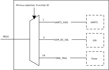
Schematic diagram of pinmux connection for PB30
Function ID {{IC_PARAM_FUNCID_FULL_MATRIX_START}}~{{IC_PARAM_FUNCID_FULL_MATRIX_END}}
When the Function ID is
{{IC_PARAM_FUNCID_FULL_MATRIX_START}}~{{IC_PARAM_FUNCID_FULL_MATRIX_END}}, full-matrix pins must be used.Taking
PA27as an example:When
PA27’s Function ID is configured as19, theUART0_TXDsignal of UART0 can be connected toPA27;When
PA27’s Function ID is configured as20, theUART0_RXDsignal of UART0 can be connected to this pin.
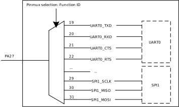
Schematic diagram of pinmux connection for PA27
Usage
Developers can connect on-chip peripheral signals to specified pins by calling the programming interface Pinmux_Config(PinName, PinFuncID).
Parameter description:
- PinName:
Pin identifier
- PinFuncID:
Specified signal ID of the on-chip peripheral controller
Based on the configured Function ID, pins can either output internal chip signals to external devices or receive signals from external devices into internal chip modules.
For the specific mapping between Function ID and pins, refer to the Pin Mux Table.
Function Group Types
Dedicated Pin Function Group:Feature: Specific peripheral signals can only be mapped to their corresponding dedicated pins. Although the number of configurable functions is relatively limited, this dedicated design can fully leverage the performance of each IP module, meeting peripheral signal quality and speed performance requirements.
Function groups: Dedicated pins are typically organized by “function groups”, where each function group contains a set of related pins.
Configuration principle: Pins within the same function group must be selected together for optimal performance.
Full-Matrix Pin Function Group:Feature: Peripheral signals can be flexibly mapped to multiple pins, providing greater configuration flexibility, but the performance of some IP modules (such as maximum transfer rate) is relatively limited.
Function ID
Function ID 0~{{IC_PARAM_FUNCID_DEDICATE_END}}
When the Function ID is
0~{{IC_PARAM_FUNCID_DEDICATE_END}}, dedicated pins must be used.Note
For example: Function ID {{IC_PARAM_FUNCID_DEDICATE_SPI0}} and Function ID {{IC_PARAM_FUNCID_FULL_MATRIX_SPI1_CLK}}~{{IC_PARAM_FUNCID_FULL_MATRIX_SPI1_CS}} are both SPI functions.
Function ID {{IC_PARAM_FUNCID_DEDICATE_SPI0}} uses dedicated pins, so the maximum SPI rate can reach 50 MHz (master mode);
Function ID {{IC_PARAM_FUNCID_FULL_MATRIX_SPI1_CLK}}~{{IC_PARAM_FUNCID_FULL_MATRIX_SPI1_CS}} uses full-matrix pins, and the maximum achievable rate is only 25 MHz (master mode).
Taking
PB5as an example: if its Function ID is configured as6, the SPISPI1_CSsignal will be directly connected to this pin via pin multiplexing.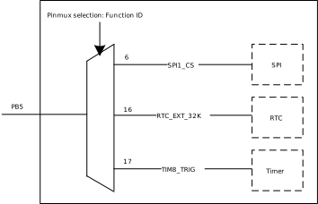
Schematic diagram of PB5 pin mux connection
Function ID {{IC_PARAM_FUNCID_FULL_MATRIX_START}}~{{IC_PARAM_FUNCID_FULL_MATRIX_END}}
When the Function ID is
{{IC_PARAM_FUNCID_FULL_MATRIX_START}}~{{IC_PARAM_FUNCID_FULL_MATRIX_END}}, full-matrix pins must be used.Taking
PA11as an example:When the Function ID of
PA11is configured as20, the UART0UART0_TXDsignal can be connected toPA11;When the Function ID of
PA11is configured as21, the UART0UART0_RXDsignal can be connected to this pin.
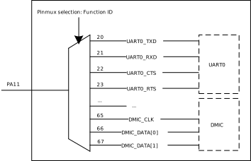
Schematic diagram of PA11 pin mux connection
Audio Function
PB11~PB19 are used for Audio function by default. Please note the following when using them:
When pin resources are sufficient, it is not recommended to multiplex them as digital functions, to avoid interference with Audio signals.
If they must be used for both Audio and digital functions simultaneously, the PCB layout must be carefully planned to ensure sufficient spacing between digital signal traces and Audio signal traces, in order to reduce the risk of mutual interference.
Usage
Developers can connect on-chip peripheral signals to specified pins by calling the programming interface Pinmux_Config(PinName, PinFuncID).
Parameter description:
- PinName:
Pin identifier
- PinFuncID:
Specified signal ID of the on-chip peripheral controller
Based on the configured Function ID, pins can either output internal chip signals to external devices or receive signals from external devices into internal chip modules.
For the specific mapping between Function ID and pins, refer to the Pin Mux Table.
Function Group Types
Dedicated Pin Function Group:Feature: Specific peripheral signals can only be mapped to their corresponding dedicated pins. Although the number of configurable functions is relatively limited, this dedicated design can fully leverage the performance of each IP module, meeting peripheral signal quality and speed performance requirements.
Function groups: Dedicated pins are typically organized by “function groups”, where each function group contains a set of related pins.
Configuration principle: Pins within the same function group must be selected together for optimal performance.
Full-Matrix Pin Function Group:Feature: Peripheral signals can be flexibly mapped to multiple pins, providing greater configuration flexibility, but the performance of some IP modules (such as maximum transfer rate) is relatively limited.
Function ID
Function ID 0~{{IC_PARAM_FUNCID_DEDICATE_END}}
When the Function ID is
0~{{IC_PARAM_FUNCID_DEDICATE_END}}, dedicated pins must be used.Note
For example: Function ID {{IC_PARAM_FUNCID_DEDICATE_SPI0}} and Function ID {{IC_PARAM_FUNCID_FULL_MATRIX_SPI1_CLK}}~{{IC_PARAM_FUNCID_FULL_MATRIX_SPI1_CS}} are both SPI functions.
Function ID {{IC_PARAM_FUNCID_DEDICATE_SPI0}} uses dedicated pins, so the maximum SPI rate can reach 50 MHz (master mode);
Function ID {{IC_PARAM_FUNCID_FULL_MATRIX_SPI1_CLK}}~{{IC_PARAM_FUNCID_FULL_MATRIX_SPI1_CS}} uses full-matrix pins, and the maximum achievable rate is only 25 MHz (master mode).
Taking
PB5as an example: if its Function ID is configured as6, the SPISPI1_CSsignal will be directly connected to this pin via pin multiplexing.
Schematic diagram of PB5 pin mux connection
Function ID {{IC_PARAM_FUNCID_FULL_MATRIX_START}}~{{IC_PARAM_FUNCID_FULL_MATRIX_END}}
When the Function ID is
{{IC_PARAM_FUNCID_FULL_MATRIX_START}}~{{IC_PARAM_FUNCID_FULL_MATRIX_END}}, full-matrix pins must be used.Taking
PA11as an example:When the Function ID of
PA11is configured as20, the UART0UART0_TXDsignal can be connected toPA11;When the Function ID of
PA11is configured as21, the UART0UART0_RXDsignal can be connected to this pin.
Schematic diagram of PA11 pin mux connection
Audio Function
PB11~PB19 are used for Audio function by default. Please note the following when using them:
When pin resources are sufficient, it is not recommended to multiplex them as digital functions, to avoid interference with Audio signals.
If they must be used for both Audio and digital functions simultaneously, the PCB layout must be carefully planned to ensure sufficient spacing between digital signal traces and Audio signal traces, in order to reduce the risk of mutual interference.
Usage
Developers can connect on-chip peripheral signals to specified pins by calling the programming interface Pinmux_Config(PinName, PinFuncID).
Parameter description:
- PinName:
Pin identifier
- PinFuncID:
Specified signal ID of the on-chip peripheral controller
Based on the configured Function ID, pins can either output internal chip signals to external devices or receive signals from external devices into internal chip modules.
For the specific mapping between Function ID and pins, refer to the Pin Mux Table.
Function Group Types
Dedicated Pin Function Group:Feature: Specific peripheral signals can only be mapped to their corresponding dedicated pins. Although the number of configurable functions is relatively limited, this dedicated design can fully leverage the performance of each IP module, meeting peripheral signal quality and speed performance requirements.
Function groups: Dedicated pins are typically organized by “function groups”, where each function group contains a set of related pins.
Configuration principle: Pins within the same function group must be selected together for optimal performance.
Full-Matrix Pin Function Group:Feature: Peripheral signals can be flexibly mapped to multiple pins, providing greater configuration flexibility, but the performance of some IP modules (such as maximum transfer rate) is relatively limited.
Function ID
Function ID 0~{{IC_PARAM_FUNCID_DEDICATE_END}}
When the Function ID is
0~{{IC_PARAM_FUNCID_DEDICATE_END}}, dedicated pins must be used.Note
For example: Function ID {{IC_PARAM_FUNCID_DEDICATE_SPI0}} and Function ID {{IC_PARAM_FUNCID_FULL_MATRIX_SPI1_CLK}}~{{IC_PARAM_FUNCID_FULL_MATRIX_SPI1_CS}} are both SPI functions.
Function ID {{IC_PARAM_FUNCID_DEDICATE_SPI0}} uses dedicated pins, so the maximum SPI rate can reach 50 MHz (master mode);
Function ID {{IC_PARAM_FUNCID_FULL_MATRIX_SPI1_CLK}}~{{IC_PARAM_FUNCID_FULL_MATRIX_SPI1_CS}} uses full-matrix pins, and the maximum achievable rate is only 25 MHz (master mode).
Taking
PB5as an example: if its Function ID is configured as6, the SPISPI1_CSsignal will be directly connected to this pin via pin multiplexing.
Schematic diagram of PB5 pin mux connection
Function ID {{IC_PARAM_FUNCID_FULL_MATRIX_START}}~{{IC_PARAM_FUNCID_FULL_MATRIX_END}}
When the Function ID is
{{IC_PARAM_FUNCID_FULL_MATRIX_START}}~{{IC_PARAM_FUNCID_FULL_MATRIX_END}}, full-matrix pins must be used.Taking
PA11as an example:When the Function ID of
PA11is configured as20, the UART0UART0_TXDsignal can be connected toPA11;When the Function ID of
PA11is configured as21, the UART0UART0_RXDsignal can be connected to this pin.
Schematic diagram of PA11 pin mux connection
Audio Function
PB11~PB19 are used for Audio function by default. Please note the following when using them:
When pin resources are sufficient, it is not recommended to multiplex them as digital functions, to avoid interference with Audio signals.
If they must be used for both Audio and digital functions simultaneously, the PCB layout must be carefully planned to ensure sufficient spacing between digital signal traces and Audio signal traces, in order to reduce the risk of mutual interference.
Usage
Developers can connect on-chip peripheral signals to specified pins by calling the programming interface Pinmux_Config(PinName, PinFuncID).
Parameter description:
- PinName:
Pin identifier
- PinFuncID:
Specified signal ID of the on-chip peripheral controller
Based on the configured Function ID, pins can either output internal chip signals to external devices or receive signals from external devices into internal chip modules.
For the specific mapping between Function ID and pins, refer to the Pin Mux Table.
Function Group Types
Dedicated Pin Function Group:Feature: Specific peripheral signals can only be mapped to their corresponding dedicated pins. Although the number of configurable functions is relatively limited, this dedicated design can fully leverage the performance of each IP module, meeting peripheral signal quality and speed performance requirements.
Function groups: Dedicated pins are typically organized by “function groups”, where each function group contains a set of related pins.
Configuration principle: Pins within the same function group must be selected together for optimal performance.
Full-Matrix Pin Function Group:Feature: Peripheral signals can be flexibly mapped to multiple pins, providing greater configuration flexibility, but the performance of some IP modules (such as maximum transfer rate) is relatively limited.
Function ID
Function ID 0~{{IC_PARAM_FUNCID_DEDICATE_END}}
When the Function ID is
0~{{IC_PARAM_FUNCID_DEDICATE_END}}, dedicated pins must be used.Note
For example: Function ID {{IC_PARAM_FUNCID_DEDICATE_SPI0}} and Function ID {{IC_PARAM_FUNCID_FULL_MATRIX_SPI1_CLK}}~{{IC_PARAM_FUNCID_FULL_MATRIX_SPI1_CS}} are both SPI functions.
Function ID {{IC_PARAM_FUNCID_DEDICATE_SPI0}} uses dedicated pins, so the maximum SPI rate can reach 50 MHz (master mode);
Function ID {{IC_PARAM_FUNCID_FULL_MATRIX_SPI1_CLK}}~{{IC_PARAM_FUNCID_FULL_MATRIX_SPI1_CS}} uses full-matrix pins, and the maximum achievable rate is only 25 MHz (master mode).
Taking
PB5as an example: if its Function ID is configured as6, the SPISPI1_CSsignal will be directly connected to this pin via pin multiplexing.
Schematic diagram of PB5 pin mux connection
Function ID {{IC_PARAM_FUNCID_FULL_MATRIX_START}}~{{IC_PARAM_FUNCID_FULL_MATRIX_END}}
When the Function ID is
{{IC_PARAM_FUNCID_FULL_MATRIX_START}}~{{IC_PARAM_FUNCID_FULL_MATRIX_END}}, full-matrix pins must be used.Taking
PA11as an example:When the Function ID of
PA11is configured as20, the UART0UART0_TXDsignal can be connected toPA11;When the Function ID of
PA11is configured as21, the UART0UART0_RXDsignal can be connected to this pin.
Schematic diagram of PA11 pin mux connection
Audio Function
PB11~PB19 are used for Audio function by default. Please note the following when using them:
When pin resources are sufficient, it is not recommended to multiplex them as digital functions, to avoid interference with Audio signals.
If they must be used for both Audio and digital functions simultaneously, the PCB layout must be carefully planned to ensure sufficient spacing between digital signal traces and Audio signal traces, in order to reduce the risk of mutual interference.
Usage
Developers can connect on-chip peripheral signals to specified pins by calling the programming interface Pinmux_Config(PinName, PinFuncID).
Parameter description:
- PinName:
Pin identifier
- PinFuncID:
The specified signal ID of the on-chip peripheral controller
Depending on the configured Function ID, a pin can either output internal chip signals to external devices or receive signals from external devices into the chip’s internal modules.
For the mapping between specific Function IDs and pins, refer to the Pin Multiplexing Table.
Function Group Types
Dedicated Pin Function Group:Characteristics: Specific peripheral signals can only be mapped to the corresponding dedicated pins. Although the number of configurable functions is relatively limited, this dedicated design fully leverages the performance of each IP module and meets the signal quality and rate performance requirements of peripheral signals.
Function groups: Dedicated pins are typically organized into “function groups”, where each function group contains a set of related pins.
Configuration principle: Pins within the same function group must be selected in combination to achieve optimal performance.
Note
RTL8730E does not include a full-matrix pin function group.
Function ID
Function ID 0~{{IC_PARAM_FUNCID_DEDICATE_END}}
Taking
PA0as an example: if its Function ID is configured to1, theUART2_RXDsignal of UART2 will be directly connected to this pin through pin multiplexing.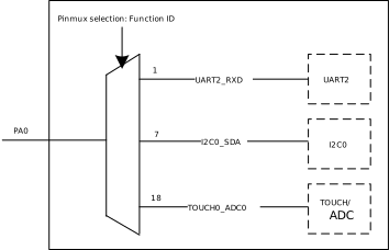
Schematic diagram of pinmux connection of PA0
Audio Function
PA18~PB6 are used for Audio function by default. Please note the following:
When pin resources are sufficient, it is not recommended to multiplex these pins for digital functions to avoid interference with Audio signals.
If they must be used for both Audio and digital functions simultaneously, PCB layout should be carefully planned to ensure sufficient spacing between digital signal traces and Audio signal traces in order to reduce the risk of mutual interference.
Usage
Developers can connect on-chip peripheral signals to a specified pin by calling the programming interface Pinmux_Config(PinName, PinFuncID).
Parameter description:
- PinName:
Pin identifier
- PinFuncID:
Specified signal ID of the on-chip peripheral controller
Depending on the configured Function ID, a pin can either output signals from the chip’s internal modules to external devices, or receive signals from external devices into the chip’s internal modules.
For the mapping between specific Function IDs and pins, refer to the Pin Multiplexing Table.
Function Group Types
Dedicated Pin Function Group:Feature: Specific peripheral signals can only be mapped to their corresponding dedicated pins. Although the number of configurable functions is relatively limited, this dedicated design fully exploits the performance of each IP module and meets peripheral signal quality and speed requirements.
Function Group: Dedicated pins are typically organized by “function groups”, where each function group contains a set of related pins.
Configuration Principle: Pins within the same function group must be selected together to achieve optimal performance.
Full-Matrix Pin Function Group:Feature: Peripheral signals can be flexibly mapped to multiple pins, providing greater configuration freedom, though the performance of some IP modules (such as maximum transfer rate) is relatively limited.
Function ID
Function ID 0~{{IC_PARAM_FUNCID_DEDICATE_END}}
When the Function ID is
0~{{IC_PARAM_FUNCID_DEDICATE_END}}, dedicated pins must be used.Note
For example: Function ID {{IC_PARAM_FUNCID_DEDICATE_SPI0}} and Function ID {{IC_PARAM_FUNCID_FULL_MATRIX_SPI1_CLK}}~{{IC_PARAM_FUNCID_FULL_MATRIX_SPI1_CS}} are both SPI functions.
Function ID {{IC_PARAM_FUNCID_DEDICATE_SPI0}} uses a dedicated pin, so the SPI function can achieve a maximum rate of 50 MHz (master mode);
Function ID {{IC_PARAM_FUNCID_FULL_MATRIX_SPI1_CLK}}~{{IC_PARAM_FUNCID_FULL_MATRIX_SPI1_CS}} uses the corresponding full-matrix pins, which can only achieve a maximum rate of 25 MHz (master mode).
Taking
PB16as an example: if its Function ID is configured to10, the SPISPI1_CSsignal will be directly connected to this pin via pin multiplexing.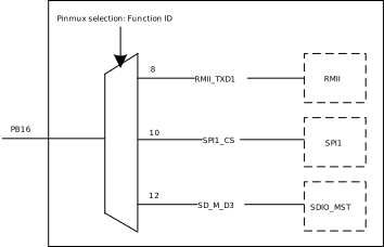
Schematic Diagram of Pin Multiplexing Connection for PB16
Function ID {{IC_PARAM_FUNCID_FULL_MATRIX_START}}~{{IC_PARAM_FUNCID_FULL_MATRIX_END}}
When the Function ID is
{{IC_PARAM_FUNCID_FULL_MATRIX_START}}~{{IC_PARAM_FUNCID_FULL_MATRIX_END}}, full-matrix pins must be used.Taking
PB19as an example:When the Function ID of
PB19is configured to95, the UART0UART0_TXDsignal can be connected toPB19;When the Function ID of
PB19is configured to96, the UART0UART0_RXDsignal can be connected to this pin.
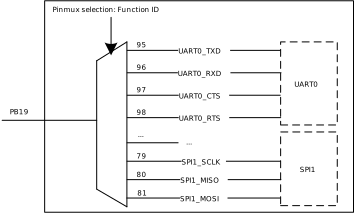
Schematic Diagram of Pin Multiplexing Connection for PB19
Usage
Developers can connect on-chip peripheral signals to specified pins by calling the programming interface Pinmux_Config(PinName, PinFuncID).
Parameter Description:
- PinName:
Pin identifier
- PinFuncID:
The specified signal ID of the on-chip peripheral controller
Depending on the configured Function ID, the pin can either output signals from the chip’s internal modules to external devices, or receive signals from external devices into the chip’s internal modules.
For the specific mapping between Function IDs and pins, refer to the Pin Multiplexing Table.
Function Group Types
Dedicated Pin Function Group:Features: Specific peripheral signals can only be mapped to their corresponding dedicated pins. Although the number of configurable functions is relatively limited, this dedicated design can fully leverage the performance of each IP module, meeting the signal quality and data rate requirements of peripherals.
Function Groups: Dedicated pins are typically organized into “function groups”, where each function group contains a set of related pins.
Configuration Principle: Pins within the same function group must be selected together to achieve optimal performance.
Full-Matrix Pin Function Group:Features: Peripheral signals can be flexibly mapped to multiple pins, providing greater configuration freedom, but the performance of some IP modules (such as maximum data transfer rate) is relatively limited.
Function ID
Function ID 0~{{IC_PARAM_FUNCID_DEDICATE_END}}
When the Function ID is in the range
0~{{IC_PARAM_FUNCID_DEDICATE_END}}, dedicated pins must be used.Note
For example: Function ID {{IC_PARAM_FUNCID_DEDICATE_SPI0}} and Function ID {{IC_PARAM_FUNCID_FULL_MATRIX_SPI1_CLK}}~{{IC_PARAM_FUNCID_FULL_MATRIX_SPI1_CS}} are both SPI functions.
Function ID {{IC_PARAM_FUNCID_DEDICATE_SPI0}} uses a dedicated pin, so the maximum SPI transfer rate can reach 50 MHz (master mode);
Function ID {{IC_PARAM_FUNCID_FULL_MATRIX_SPI1_CLK}}~{{IC_PARAM_FUNCID_FULL_MATRIX_SPI1_CS}} uses the corresponding full-matrix pin, where the maximum achievable rate is only 25 MHz (master mode).
Taking
PA9as an example: if its Function ID is configured as9, theSD_S_CMDsignal of SDIO_DEVICE will be directly connected to this pin through pin multiplexing.
Schematic Diagram of Pin Multiplexing Connection for PA9
Function ID {{IC_PARAM_FUNCID_FULL_MATRIX_START}}~{{IC_PARAM_FUNCID_FULL_MATRIX_END}}
When the Function ID is in the range
{{IC_PARAM_FUNCID_FULL_MATRIX_START}}~{{IC_PARAM_FUNCID_FULL_MATRIX_END}}, full-matrix pins must be used.Taking
PA24as an example:When the Function ID of
PA24is configured as65, theUART0_TXDsignal of UART0 can be connected toPA24;When the Function ID of
PA24is configured as66, theUART0_RXDsignal of UART0 can be connected to this pin.

Schematic Diagram of Pin Multiplexing Connection for PA24
Usage Method
Developers can connect pins to specified on-chip peripheral signals by calling the programming interface Pinmux_Config(PinName, PinFuncID).
Parameter description:
- PinName:
Pin identifier
- PinFuncID:
Specified signal ID of the on-chip peripheral controller
Based on the configured function-id, pins can either output internal chip signals to external devices or receive signals input from external devices to internal chip modules.
For specific pin to function-id mappings, please refer to Pinmux Table.
Function ID
Function ID 0-15
Each pin can only connect to fixed signals of specific IPs.
Take
PA0as an example: When configured with Function ID0, this pin will be directly connected toADC0through pin multiplexing.Refer to the Pinmux Table for specific function assignments supported by each pin.
Trap Pins
Note
Before development, please pay attention to the following pin multiplexing considerations to avoid unexpected behavior.
During the power-on process, the chip’s internal circuitry latches the voltage levels of certain pins to determine the operating mode of the chip. Therefore, when designing hardware or using development boards, configure them correctly according to the hardware design guide for the corresponding chip to avoid abnormal operation. After startup is complete, Trap Pins behave the same as other pins and can be configured for other functions normally.
Pin Name |
Symbol |
Active Level |
Description |
|---|---|---|---|
PB31 |
TM_DIS |
Low |
|
PB5 |
UD_DIS |
Low |
Note Disabling the download mode is controlled by OTP-related fields. When UART download is disabled via OTP, the power-on latch state of this pin is invalid. |
Pin Name |
Symbol |
Active Level |
Description |
|---|---|---|---|
PA1 |
TM_DIS |
Low |
|
PA20 |
UD_DIS |
Low |
Note Disabling download mode is controlled by OTP-related fields. When UART download is disabled by OTP, the power-on latched state of this pin is invalid. |
PA22 |
PSO_SEL |
- |
|
Pin Name |
Symbol |
Active Level |
Description |
|---|---|---|---|
PA1 |
TM_DIS |
Low |
|
PA20 |
UD_DIS |
Low |
Note Disabling download mode is controlled by OTP-related fields. When UART download is disabled by OTP, the power-on latched state of this pin is invalid. |
PA22 |
PSO_SEL |
- |
|
Pin Name |
Symbol |
Active Level |
Description |
|---|---|---|---|
PA1 |
TM_DIS |
Low |
|
PA20 |
UD_DIS |
Low |
Note Disabling download mode is controlled by OTP-related fields. When UART download is disabled by OTP, the power-on latched state of this pin is invalid. |
PA22 |
PSO_SEL |
- |
|
Pin Name |
Symbol |
Active Level |
Description |
|---|---|---|---|
PA1 |
TM_DIS |
Low |
|
PA20 |
UD_DIS |
Low |
Note Disabling download mode is controlled by OTP-related fields. When UART download is disabled by OTP, the power-on latched state of this pin is invalid. |
PA22 |
PSO_SEL |
- |
|
Pin Name |
Symbol |
Active Level |
Description |
|---|---|---|---|
PB22 |
TM_DIS |
Low |
|
PB24 |
UD_DIS |
Low |
Note When OTP disables UART download, the power-on latch state of this pin is invalid. |
PB21 |
BOOT_SEL |
- |
Note When OTP-related fields are programmed, OTP state takes priority for selection. |
Pin Name |
Symbol |
Active Level |
Description |
|---|---|---|---|
PA3 |
TM_DIS |
Low |
|
PB20 |
UD_DIS |
Low |
Note Disabling download mode is controlled by OTP-related fields. Once UART download is disabled via OTP, the power-on latch state of this pin becomes invalid. |
PB18 |
BOOT_SEL |
- |
Note BOOT_SEL is controlled by OTP-related fields. Once the OTP-related fields are programmed, the selection is made based on the OTP programmed state with higher priority. |
Pin Name |
Symbol |
Active Level |
Description |
|---|---|---|---|
PA22 |
TM_DIS |
Low |
|
PA19 |
UD_DIS |
Low |
Note The disable download mode is controlled by OTP-related fields. When UART download is disabled by OTP, the power-on latch state of this pin is invalid. |
Pin name |
Symbol |
Active level |
Description |
|---|---|---|---|
PA4 |
OTPBYP |
High |
|
PA5 |
TEST_MODE_SEL |
High |
|
PE16 |
PG_MODE_SEL |
High |
|
PE2 |
BOOT_SOURCE |
- |
|
PE0 |
TEST_MODE_ID_0 |
- |
|
PE13 |
TEST_MODE_ID_1 |
- |
|
PE14 |
TEST_MODE_ID_2 |
- |
|
Note
When OTP fields are programmed, priority is given to the programmed OTP status.
Note
Please configure the external pull-up/pull-down resistors for each Trap Pin correctly to ensure the pin logic levels during power-on meet expectations. Refer to the datasheet for details.
Wakeup Pins
Regular GPIO pins support waking the system from CG and PG sleep modes.
Wake pins (
PB30andPB31) are directly connected to the wake-up circuit; in addition to waking from CG and PG sleep modes, they can also wake the system from deep sleep mode.
Warning
If these pins need to be configured for other peripheral functions, disable the wake-up function first to avoid accidental wake-up triggered by pin signal changes.
Wake pins may be multiplexed with Trap pins. When multiplexed, ensure that the logic level of the Trap pin after wake-up does not cause the system to enter an unintended operating mode.
General GPIO pins support waking the system from CG and PG sleep modes.
Wake-up pins (
PA0andPA1) are directly connected to the wake-up circuit, and can wake the system from deep sleep mode in addition to CG and PG sleep modes.
Warning
If these pins need to be configured for other peripheral functions, disable the wake-up functionality first to avoid unexpected wake-ups triggered by pin signal changes.
Wake-up pins may be multiplexed with Trap pins. When multiplexing, ensure that the logic level of the Trap pin after wake-up does not cause the system to enter an unintended operating mode.
General GPIO pins support waking the system from CG and PG sleep modes.
Wake-up pins (
PA0andPA1) are directly connected to the wake-up circuit, and can wake the system from deep sleep mode in addition to CG and PG sleep modes.
Warning
If these pins need to be configured for other peripheral functions, disable the wake-up functionality first to avoid unexpected wake-ups triggered by pin signal changes.
Wake-up pins may be multiplexed with Trap pins. When multiplexing, ensure that the logic level of the Trap pin after wake-up does not cause the system to enter an unintended operating mode.
General GPIO pins support waking the system from CG and PG sleep modes.
Wake-up pins (
PA0andPA1) are directly connected to the wake-up circuit, and can wake the system from deep sleep mode in addition to CG and PG sleep modes.
Warning
If these pins need to be configured for other peripheral functions, disable the wake-up functionality first to avoid unexpected wake-ups triggered by pin signal changes.
Wake-up pins may be multiplexed with Trap pins. When multiplexing, ensure that the logic level of the Trap pin after wake-up does not cause the system to enter an unintended operating mode.
General GPIO pins support waking the system from CG and PG sleep modes.
Wake-up pins (
PA0andPA1) are directly connected to the wake-up circuit, and can wake the system from deep sleep mode in addition to CG and PG sleep modes.
Warning
If these pins need to be configured for other peripheral functions, disable the wake-up functionality first to avoid unexpected wake-ups triggered by pin signal changes.
Wake-up pins may be multiplexed with Trap pins. When multiplexing, ensure that the logic level of the Trap pin after wake-up does not cause the system to enter an unintended operating mode.
General GPIO pins support waking the system from CG and PG sleep modes.
Wake-up pins (
PB21~PB24) are directly connected to the wake-up circuit, and can wake the system from deep sleep mode in addition to CG and PG sleep modes.
Warning
If these pins need to be configured for other peripheral functions, disable the wake-up function first to avoid unintended wake-up triggered by pin signal changes.
Wake-up pins may be multiplexed with Trap pins. When multiplexed, ensure the logic level of the Trap pin after wake-up does not cause the system to enter an unintended operating mode.
General GPIO pins support waking the system from CG and PG sleep modes.
Wake-up pins (
PA0~PA3) are directly connected to the wake-up circuit, and can wake the system from deep sleep mode in addition to CG and PG sleep modes.
Warning
If these pins need to be configured for other peripheral functions, disable the wake-up function first to avoid unintended wake-ups triggered by pin signal changes.
Wake-up pins may be multiplexed with Trap pins. When multiplexing, ensure that the logic level of the Trap pin after wake-up does not cause the system to enter an unintended operating mode.
Normal GPIO pins support waking the system from CG and PG sleep modes.
Wake-up pins (
PA19~PA22) are directly connected to the wake-up circuit, and can wake the system from deep sleep mode in addition to CG and PG sleep modes.
Warning
If these pins need to be configured for other peripheral functions, disable the wake-up function first to avoid accidental wake-up triggered by pin signal changes.
Wake-up pins may be multiplexed with Trap pins. When multiplexed, ensure that the logic level of the Trap pins after wake-up does not cause the system to enter an unintended operating mode.
Wake-up pins (
PA0~PA3) are directly connected to wake-up circuits, and can wake the system fromDSLPandPGmodes.Wake-up pins (
PF0~PF17) are directly connected to wake-up circuits, and can wake the system fromPGmode.
Warning
Disable wake-up functionality before multiplexing these two pins.
Wake-up pins may be multiplexed with Trap pins.
When multiplexing, ensure the Trap pin’s signal level after wake-up does not cause the system to enter unexpected modes.
Note
For specific configuration methods of the wakeup function (such as enabling/disabling wakeup sources, configuring wakeup trigger conditions, etc.), refer to the Power Saving section.
SWD Pins
{{IC_PARAM_SWD_CLK_PIN}} and {{IC_PARAM_SWD_DATA_PIN}} are the default pins for the SWD debug interface.
Note
When the following log message appears, it indicates that the {{IC_PARAM_SWD_CLK_PIN}} or {{IC_PARAM_SWD_DATA_PIN}} pin has already been configured to another module, and it is no longer possible to connect to the debugger through that pin.
SWD PAD PortX_PinYY is configured to funcIDZZ
If you still need to connect a debugger, refer to Function Mux to reconfigure the pin for the SWD signal.
{{IC_PARAM_SWD_CLK_PIN}} and {{IC_PARAM_SWD_DATA_PIN}} are the default pins for the SWD debug interface.
Note
When the following log message appears, it indicates that the {{IC_PARAM_SWD_CLK_PIN}} or {{IC_PARAM_SWD_DATA_PIN}} pin has already been configured to another module, and it is no longer possible to connect to the debugger through that pin.
SWD PAD PortX_PinYY is configured to funcIDZZ
If you still need to connect a debugger, refer to Function Mux to reconfigure the pin for the SWD signal.
{{IC_PARAM_SWD_CLK_PIN}} and {{IC_PARAM_SWD_DATA_PIN}} are the default pins for the SWD debug interface.
Note
When the following log message appears, it indicates that the {{IC_PARAM_SWD_CLK_PIN}} or {{IC_PARAM_SWD_DATA_PIN}} pin has already been configured to another module, and it is no longer possible to connect to the debugger through that pin.
SWD PAD PortX_PinYY is configured to funcIDZZ
If you still need to connect a debugger, refer to Function Mux to reconfigure the pin for the SWD signal.
{{IC_PARAM_SWD_CLK_PIN}} and {{IC_PARAM_SWD_DATA_PIN}} are the default pins for the SWD debug interface.
Note
When the following log message appears, it indicates that the {{IC_PARAM_SWD_CLK_PIN}} or {{IC_PARAM_SWD_DATA_PIN}} pin has already been configured to another module, and it is no longer possible to connect to the debugger through that pin.
SWD PAD PortX_PinYY is configured to funcIDZZ
If you still need to connect a debugger, refer to Function Mux to reconfigure the pin for the SWD signal.
{{IC_PARAM_SWD_CLK_PIN}} and {{IC_PARAM_SWD_DATA_PIN}} are the default pins for the SWD debug interface.
Note
When the following log message appears, it indicates that the {{IC_PARAM_SWD_CLK_PIN}} or {{IC_PARAM_SWD_DATA_PIN}} pin has already been configured to another module, and it is no longer possible to connect to the debugger through that pin.
SWD PAD PortX_PinYY is configured to funcIDZZ
If you still need to connect a debugger, refer to Function Mux to reconfigure the pin for the SWD signal.
{{IC_PARAM_SWD_CLK_PIN}} and {{IC_PARAM_SWD_DATA_PIN}} are the default pins for the SWD debug interface.
Note
When the following log message appears, it indicates that the {{IC_PARAM_SWD_CLK_PIN}} or {{IC_PARAM_SWD_DATA_PIN}} pin has already been configured to another module, and it is no longer possible to connect to the debugger through that pin.
SWD PAD PortX_PinYY is configured to funcIDZZ
If you still need to connect a debugger, refer to Function Mux to reconfigure the pin for the SWD signal.
{{IC_PARAM_SWD_CLK_PIN}} and {{IC_PARAM_SWD_DATA_PIN}} are the default pins for the SWD debug interface.
Note
When the following log message appears, it indicates that the {{IC_PARAM_SWD_CLK_PIN}} or {{IC_PARAM_SWD_DATA_PIN}} pin has already been configured to another module, and it is no longer possible to connect to the debugger through that pin.
SWD PAD PortX_PinYY is configured to funcIDZZ
If you still need to connect a debugger, refer to Function Mux to reconfigure the pin for the SWD signal.
{{IC_PARAM_SWD_CLK_PIN}} and {{IC_PARAM_SWD_DATA_PIN}} are the default pins for the SWD debug interface.
Note
When the following log message appears, it indicates that the {{IC_PARAM_SWD_CLK_PIN}} or {{IC_PARAM_SWD_DATA_PIN}} pin has already been configured to another module, and it is no longer possible to connect to the debugger through that pin.
SWD PAD PortX_PinYY is configured to funcIDZZ
If you still need to connect a debugger, refer to Function Mux to reconfigure the pin for the SWD signal.
Pins PE_1 and PE_2 are forcibly locked to the SWD function by default.
If you want to multiplex these two pins, you must first disable the SWD function, which is already handled by the programming interface Pinmux_Config().
Note
When the following log message appears, it indicates that PE_1 or PE_2 has been connected to another module, and you can no longer connect the debugger via that pin.
If you still need to connect the debugger, please refer to Function Mux to reconfigure the pins for the SWD signals.
SWD PAD PortX_PinYY is configured to funcIDZZ
Raw API
PINMUX Exported Constants
PINMUX Peripheral Location Definitions
/* Peripheral pinmux location selection 0. */
#define PINMUX_S0 (0)

/* Peripheral pinmux location selection 1. */
#define PINMUX_S1 (1)

/* Peripheral pinmux location selection 2. */
#define PINMUX_S2 (2)

/* Peripheral pinmux location selection 3. */
#define PINMUX_S3 (3)

/* Peripheral pinmux location selection 4. */
#define PINMUX_S4 (4)

/* Peripheral pinmux location selection 5. */
#define PINMUX_S5 (5)
PINMUX Port and Pin Definitions
/* Extract port number from pin name. */
#define PORT_NUM ((pin>>5) & 0x03)

/* Extract pin number from pin name. */
#define PIN_NUM (pin & 0x1f)
PINMUX Exported Functions
-
void Pinmux_Config(u8 PinName, u32 PinFunc)
Set the function type of one pin.
- Parameters:
PinName – Target pin. This parameter must be one of the values defined in PINMUX_Pin_Name_definitions.
PinFunc – The function type for the pin, value of PINMUX_Function_definitions.
-
u32 Pinmux_ConfigGet(u8 PinName)
Get the function type of one pin.
- Parameters:
PinName – Target pin. This parameter must be one of the values defined in PINMUX_Pin_Name_definitions.
- Returns:
The function type for the pin, value of PINMUX_Function_definitions.
-
void Pinmux_Swdoff(void)
Turn off pinmux SWD function.
Note
When multiplexing shared SWD pins to other functions, this function must be called.
Pin Control
Overview
Depending on user requirements, the chip’s I/O ports can be flexibly configured. For details, see I/O Block Diagram.
This section mainly introduces the features supported by I/O ports and programming methods. For the configuration methods of connecting I/O ports to on-chip peripheral signals, refer to the Pin Mux section.
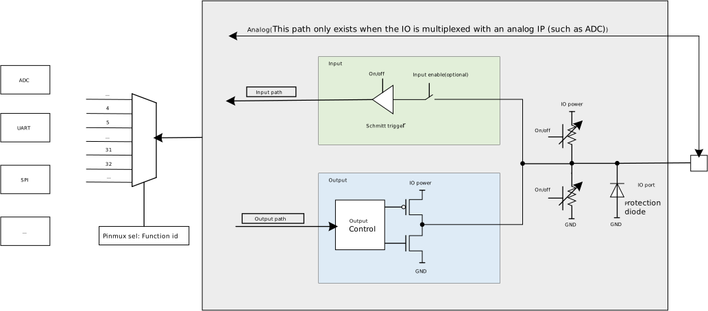
I/O Block Diagram
Features
Each pin supports the following electrical characteristic configurations:
Internal pull-up/pull-down resistors
Supports independent pull-up/pull-down/high-impedance control
Pull resistance values are adjustable for certain pins
Multiple drive strength levels
Multiple drive strength levels are available. The maximum level is used by default unless otherwise specified.
Adjustable slew rate control
Supports signal edge output at different slew rates. This feature is supported only on certain pins.
Note
For I/O port characteristic parameters such as pull resistance values, drive strength, voltage characteristics, and signal slew rate, please refer to the Chip Datasheet. Drive strength values and the number of levels may vary between pins.
Pin State Management in Low-Power Mode
The pull-up/pull-down (PU/PD) states of I/O ports in Active mode and low-power modes are controlled by separate independent registers. The default PU/PD states of each pin during initialization are defined uniformly in
ameba_pinmapcfg
and loaded by pinmap_init() at system startup.
Pin Input State
Normal Sleep Mode (PG or CG)
The PU/PD function of all I/O ports takes effect.
Deep Sleep Mode (DSLP)
The PU/PD function of most I/O ports remains effective;
The power supply of some I/O ports will be cut off, causing the PU/PD of these pins to become invalid and leaving the pins in a floating state.
If the circuit connected to these I/O ports needs to be pulled high or low, a dedicated pull-up/pull-down circuit must be designed in the external circuitry of the chip.
Note
For I/O ports whose PU/PD function becomes invalid in Deep Sleep Mode, refer to the chip datasheet.
Pin Output State
Normal Sleep Mode (PG or CG)
The I/O port output will retain the logic level before entering sleep.
For example, if an I/O is configured to output 1 before sleep, after the system enters PG or CG, the I/O will still maintain output 1 unchanged.
Deep Sleep Mode (DSLP)
The high/low logic level output state set during the Active phase will be lost.
For example, if an I/O is configured to output 1 before sleep, after the system enters Deep Sleep Mode, the I/O will no longer maintain the output 1 state.
I/O Ports Special Power Group
I/O ports are managed in groups by power domain. The supported operating voltages vary across groups (e.g., some groups support both 1.8V and 3.3V, while others support only 3.3V). For complete pin power group information, refer to the chip datasheet.
This section lists only the pin groups with special power supply constraints.
None.
PB11~PB19: Used for Audio function by default. The I/O supply voltage is fixed at 1.8V, regardless of the actual mux function.
PB11~PB19: Used for Audio function by default. The I/O supply voltage is fixed at 1.8V, regardless of the actual mux function.
PB11~PB19: Used for Audio function by default. The I/O supply voltage is fixed at 1.8V, regardless of the actual mux function.
PB11~PB19: Used for Audio function by default. The I/O supply voltage is fixed at 1.8V, regardless of the actual mux function.
PA18~PB6: Used for Audio function by default. The I/O supply voltage is fixed at 1.8V, regardless of the actual mux function.
None.
The I/O supply voltage of PA23 and PA24 (group G3) supports 5V, 3.3V, or 1.8V. The default is 5V, which can be adjusted via the PAD_G3IOVoltCtrl interface.
Raw API
PAD Exported Constants
PAD Drive Strength Definitions
/* PAD drive strength lowest level. */
#define PAD_DRV_ABILITITY_LOW (0)

/* PAD drive strength mid-low level. */
#define PAD_DRV_ABILITITY_MID_LOW (1)

/* PAD drive strength mid-high level. */
#define PAD_DRV_ABILITITY_MID_HIGH (2)

/* PAD drive strength highest level. */
#define PAD_DRV_ABILITITY_HIGH (3)
PAD Pull Resistor Definitions
/* PAD large pull resistor. */
#define PAD_Resistor_LARGE 0x00

/* PAD small pull resistor. */
#define PAD_Resistor_SMALL 0x01
PAD Slew Rate Definitions
/* PAD output slew rate fast. */
#define PAD_SlewRate_Fast (0)

/* PAD output slew rate slow. */
#define PAD_SlewRate_Slow (1)
PAD Exported Functions
-
void PAD_CMD(u8 PinName, u8 NewStatus)
Set the Internal pad shutdown or enable mode.
- Parameters:
PinName – Target pin. This parameter must be one of the values defined in PINMUX_Pin_Name_definitions.
NewStatus – Enable or disable (shutdown)
-
void PAD_DrvStrength(u8 PinName, u32 DrvStrength)
Set the driving strength of the specified PAD.
- Parameters:
PinName – Target pin. This parameter must be one of the values defined in PINMUX_Pin_Name_definitions.
DrvStrength – PAD driving strength. This parameter can be a value of PAD Drive Strength Definitions.
-
void PAD_InputCtrl(u8 PinName, u32 NewState)
Control digital path input.
- Parameters:
PinName – Target pin. This parameter must be one of the values defined in PINMUX_Pin_Name_definitions.
NewState –
Digital path input status.
ENABLE: Enable digital path input.
DISABLE: Disable digital path input.
-
void PAD_PullCtrl(u8 PinName, u8 PullType)
Set the internal PAD pull type.
- Parameters:
PinName – Target pin. This parameter must be one of the values defined in PINMUX_Pin_Name_definitions.
PullType –
Pull type for the pin. This parameter can be one of the following values:
GPIO_PuPd_NOPULL
GPIO_PuPd_DOWN
GPIO_PuPd_UP
-
void PAD_ResistorCtrl(u8 PinName, u8 RType)
Set the internal PAD resistor type.
- Parameters:
PinName – Target pin. This parameter must be one of the values defined in PINMUX_Pin_Name_definitions.
RType –
Resistor type for the pin. This parameter can be one of the following values:
PAD_Resistor_LARGE
PAD_Resistor_SMALL
-
void PAD_SchmitCtrl(u8 PinName, u32 NewState)
Set the PAD Schmitt trigger control status.
- Parameters:
PinName – Target pin. This parameter must be one of the values defined in PINMUX_Pin_Name_definitions.
NewState – Specify the control status. Refer to the datasheet for detail informations. This parameter can be: ENABLE or DISABLE.
-
void PAD_SleepPullCtrl(u8 PinName, u8 PullType)
Set the internal PAD pull type in sleep and deepsleep mode. The hardware will automatically switch to the sleep pull control when the system enters sleep or deepsleep mode. The hardware will automatically switch to the function pull control when the system wakes up from sleep mode.
- Parameters:
PinName – Target pin. This parameter must be one of the values defined in PINMUX_Pin_Name_definitions.
PullType –
Pull type for the pin. This parameter can be one of the following values:
GPIO_PuPd_NOPULL
GPIO_PuPd_DOWN
GPIO_PuPd_UP
-
void PAD_SlewRateCtrl(u8 PinName, u32 NewState)
Set the PAD slew rate control status.
- Parameters:
PinName – Target pin. This parameter must be one of the values defined in PINMUX_Pin_Name_definitions.
NewState –
Specify the slew rate control status. Refer to the datasheet for detail informations. This parameter can be one of the following values:
PAD_SlewRate_Slow
PAD_SlewRate_Fast
Not supported.
-
void APAD_InputCtrl(u8 PinName, u32 NewState)
Control digital path input for Audio share PAD.
- Parameters:
PinName – Pin of Audio share PAD or 0xFF.
NewState –
Digital path input status.
ENABLE: Enable digital path input.
DISABLE: Disable digital path input.
Note
Only valid for Audio share PADs.
If PinName is 0xFF, all the pins of Audio share PAD will be controlled.
FUNCTION_REF=APAD_InputCtrl
FUNCTION_REF=APAD_InputCtrl
FUNCTION_REF=APAD_InputCtrl
FUNCTION_REF=APAD_InputCtrl
Not supported.
Not supported.