Pseudo-Static Random Access Memory (PSRAM)
Overview
PSRAM (Pseudo Static Random Access Memory) is a type of memory that combines the ease of use of SRAM with the high-density characteristics of DRAM. It integrates a refresh controller internally and is completely transparent to software. As a result, it can be randomly read and written by address through a simple interface just like SRAM, while providing a storage capacity close to that of DRAM at a lower cost per unit.
The chip communicates with PSRAM through the PSRAM controller (PSRAMC) to achieve high-speed data transfer, making it suitable for application scenarios such as audio/video processing and image transmission, which require a large data buffer and have certain bandwidth requirements.
Features
PSRAM Device Features
Storage cell: Based on the DRAM capacitor structure, with an integrated internal refresh controller.
Parallel interface: Data lines (DQ0~DQn) and control signals (CS, CK/CK#, DQS, RESET).
Automatic refresh: The internal refresh controller periodically maintains data integrity without software intervention.
Temperature-adaptive refresh: An integrated temperature sensor automatically shortens the refresh interval at high temperatures (>85°C) to guarantee data reliability, and lengthens the interval at normal temperatures to reduce power consumption.
High-speed access: Supports the DDR (Double Data Rate) transfer mode, suitable for high-bandwidth data processing.
Burst access: Supports reading and writing consecutive addresses, improving data transfer efficiency.
Random access: Allows reading and writing data at any address.
Low-power modes: Supports two states, half-sleep and Deep-sleep. In Deep-sleep mode, all refresh operations stop and data is lost.
PSRAM Controller Features
Clock frequency: up to 200 MHz
Supports Double Data Rate (DDR)
8-bit data width (DQ8)
Supports PHY-layer automatic calibration
Supports half-sleep and deep power-down modes
Software-configurable drive strength
Transparent to software: simply access the base address (0x6000_0000) to access PSRAM memory.
Clock frequency: up to 250 MHz
Supports Double Data Rate (DDR)
8-bit data width (DQ8)
Supports PHY-layer automatic calibration
Supports half-sleep and deep power-down modes
Software-configurable drive strength
Transparent to software: simply access the base address (0x6000_0000) to access PSRAM memory.
Clock frequency: up to 250 MHz
Supports Double Data Rate (DDR)
8-bit data width (DQ8)
Supports PHY-layer automatic calibration
Supports half-sleep and deep power-down modes
Software-configurable drive strength
Transparent to software: simply access the base address (0x6000_0000) to access PSRAM memory.
Clock frequency: up to 250 MHz
Supports Double Data Rate (DDR)
8-bit data width (DQ8)
Supports PHY-layer automatic calibration
Supports half-sleep and deep power-down modes
Software-configurable drive strength
Transparent to software: simply access the base address (0x6000_0000) to access PSRAM memory.
Clock frequency: up to 250 MHz
Supports Double Data Rate (DDR)
8-bit data width (DQ8)
Supports PHY-layer automatic calibration
Supports half-sleep and deep power-down modes
Software-configurable drive strength
Transparent to software: simply access the base address (0x6000_0000) to access PSRAM memory.
Clock frequency: up to 230 MHz
Supports Double Data Rate (DDR)
8-bit data width (DQ8)
Supports PHY-layer automatic calibration
Supports half-sleep and deep power-down modes
Software-configurable drive strength
Transparent to software: simply access the base address (0x6000_0000) to access PSRAM memory.
Clock frequency: up to 200 MHz
Supports Double Data Rate (DDR)
8/16-bit data width (DQ8/16)
Supports PHY-layer automatic calibration
Supports half-sleep and deep power-down modes
Software-configurable drive strength
Transparent to software: simply access the base address (0x6000_0000) to access PSRAM memory.
Clock frequency: up to 200 MHz
Supports Double Data Rate (DDR)
8-bit data width (DQ8)
Supports PHY-layer automatic calibration
Supports half-sleep and deep power-down modes
Software-configurable drive strength
Transparent to software: simply access the base address (0x6000_0000) to access PSRAM memory.
Architecture
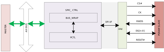
The structure of PSRAMC is shown in the figure below, which is divided into two parts: the PHY layer and the SPIC controller:
PHY layer: The physical layer, responsible for timing calibration, programmable drive strength configuration, and signal integrity enhancement, interfacing directly with the PSRAM device.
SPIC controller: The control layer, responsible for timing control, protocol conversion, arbitration, and refresh scheduling. Masters such as the CPU and DMA access the SPIC through the AXI bus, thereby accessing the PSRAM device.
Usage Guide
PSRAM Initialization
Automatic Initialization After Boot
After the device boots, the Bootloader automatically determines whether the chip integrates PSRAM, then performs model detection, select the optimal clock frequency and completes initialization without user intervention. An example of the initialization startup log is as follows:
[PSRAM-I] PSRAM Ctrl CLK: 400000000 Hz
[BOOT-I] Init WB PSRAM
DQS Delay Calibration
PSRAM stays synchronized through an additional DQS (Data Strobe) signal line and the DQ (Data) signal line. Affected by factors such as trace length and the internal path of the chip, a phase offset may occur between DQS and DQ, resulting in sampling errors. Therefore, after initialization is complete, the chip automatically performs DQS delay calibration: by dynamically adjusting the phase alignment between DQS and DQ, it optimizes the signal sampling window.
An example of a successful calibration startup log is as follows:
[PSRAM-I] Cal win size 16
Note
When the calibration window size Cal win size is less than 9, it is considered a calibration failure. In this case, it is recommended to check the signal integrity or appropriately reduce the PSRAM clock frequency; if the calibration still cannot pass, please contact Realtek.
Memory Layout Planning
Select the Link Option for PSRAM through menuconfig, as follows:
----MENUCONFIG FOR General----
...
CONFIG Link Option  --->
        IMG1(Bootloader) running on FLASH or SRAM? (FLASH)  --->
        IMG2(Application) running on FLASH or PSRAM? (FLASH)  --->
            (X) FLASH
            ( ) SRAM
            ( ) PSRAM
         IMG2 Data and Heap in SRAM or PSRAM? (SRAM)
            (X) SRAM
            ( ) PSRAM
    [*] ALL PSRAM USED FOR APPLICATION HEAP
...
The options above determine where each firmware image and data segment is stored:
IMG2(Application) running on FLASH or PSRAM: Selects the execution space for the application code (IMG2). Selecting
PSRAMplaces the application code in PSRAM for execution, relieving Flash capacity or bandwidth pressure.IMG2 Data and Heap in SRAM or PSRAM: Selects the storage location for the application data segment and Heap. When the data volume is large,
PSRAMcan be selected.ALL PSRAM USED FOR APPLICATION HEAP: When checked, all PSRAM space is allocated to the application Heap.
Note
For the specific impact of each configuration on the memory layout, refer to RAM Memory Layout .
If the following message appears in the startup log, it means that the PSRAM size in the current memory layout does not match the actual size of the PSRAM device. You need to update the value of PSRAM_END in ameba_layout.ld to the actual end address of the PSRAM device.
[PSRAM-W] PSRAM_END mismatch: layout=0x60400000, actual=0x60800000, please update ameba_layout.ld
Usage Notes
Using PSRAM in High-Temperature Environments
PSRAM relies on periodic refresh to maintain data integrity. To avoid refresh operations monopolizing bandwidth, PSRAMC adopts a distributed refresh strategy: refresh commands are evenly distributed into the gaps between normal accesses, transparently to software. The maximum interval of distributed refresh is determined by TCEM (Chip Select Low-Level Maximum Time).
The TCEM parameter is preset by the SDK, and the chip may use the Standard Refresh Mode intended for normal temperatures. If the application involves high temperatures (T > 85°C), the user must modify the code as described below to ensure data reliability.
Configuration Rules:
The refresh rules of PSRAM in different temperature ranges are shown in the table below:
Temperature range |
Refresh strategy |
Max. refresh interval |
|---|---|---|
T ≤ 85°C |
Standard Refresh Mode |
4μs |
85°C < T ≤ 125°C |
Enhanced Refresh Mode |
1μs |
Modification Steps:
Locate the code file.
Open the
ameba_psram.cfile in the SDK and find the functionPSRAM_CTRL_Init().Modify the code.
Psram_Tcem_T25is the parameter macro for normal temperature (T ≤ 85°C), andPsram_Tcem_T85is the parameter macro for high temperature (T > 85°C, corresponding to the Enhanced Refresh Mode in the table above). In high-temperature scenarios, keep everything else unchanged and simply changePsram_Tcem_T25toPsram_Tcem_T85.psram_ctrl->TPR0 = (CS_TCEM(Psram_Tcem_T85 * 1000 / PsramInfo.PSRAMC_Clk_Unit / 32) | (TPR0_OTHER_FIELDS));
Row Hammer Effect Mitigation
Physical Mechanism and Risk
Cause: High-frequency accesses to a target row (Aggressor Row) can cause the capacitors of the adjacent rows (Victim Rows) to leak charge abnormally due to charge-leakage characteristics.
Consequence: This triggers single-bit upsets (SEU) or multi-bit upsets (MBU), leading to data corruption.
Mitigation Solutions
Distributed row refresh: Performed automatically by hardware, evenly distributing refresh operations to avoid concentrated high-frequency accesses.
Access dilution via Cache: In a PSRAM system with Cache enabled, the Cache significantly reduces the probability of Row Hammer by lowering the frequency of direct accesses to physical memory:
Prefetch buffering: Merges random accesses into burst transfers, reducing the number of physical row activations.
Write merging: Aggregates scattered write operations, reducing the frequency of row address switching.
Note
Normal usage scenarios will not incur high-frequency activation accesses to the same row. If you do have such an application scenario and it triggers bit flips in adjacent rows, please contact Realtek.