LCD Controller (LCDC)
Supported ICs[ RTL8721F ]
Introduction
The Liquid Crystal Display Controller (LCDC) is used to fetch display data from main memory and output with MIPI-DSI interface. MIPI-DSI supports several formats, or packet sequences. The following figure illustrates the video mode data transmission.
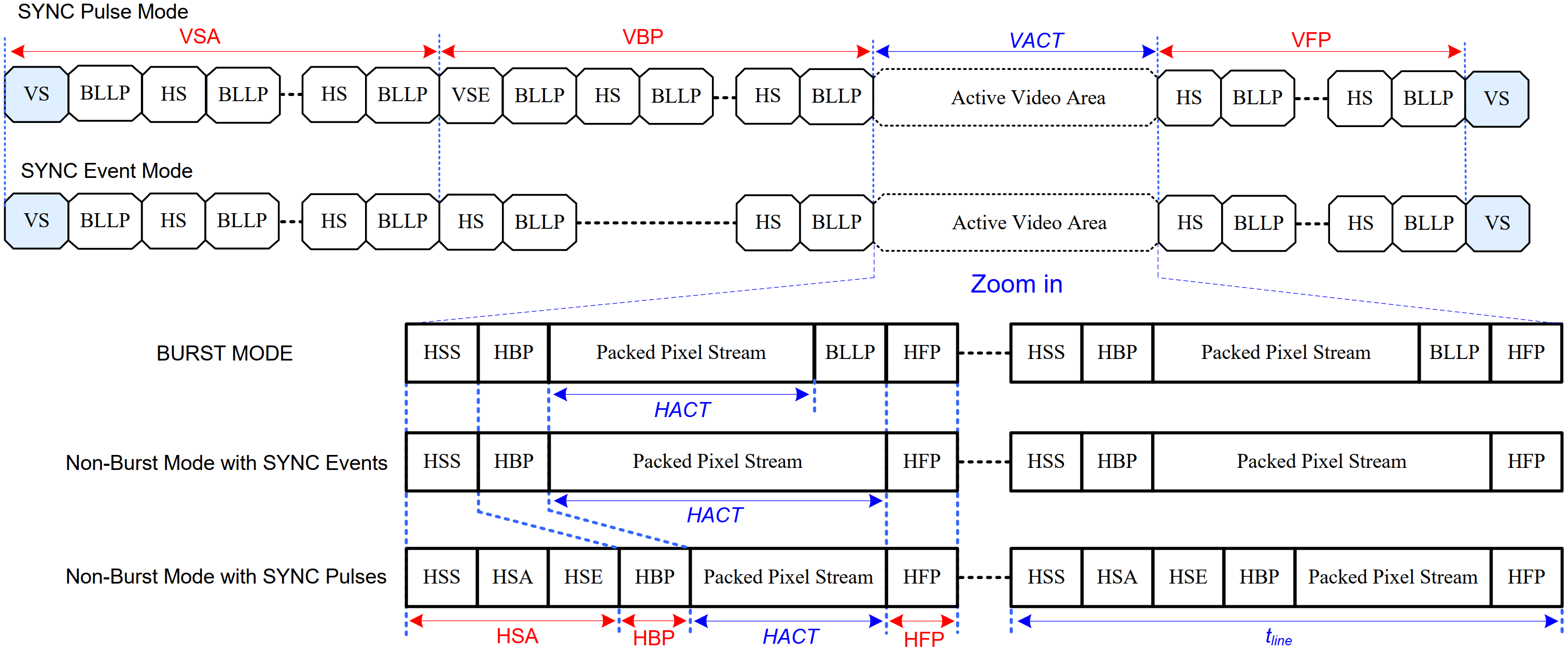
DSI packets
Normally, RGB pixel data is sent with one full scanline of pixels in a single packet. And during the BLLP the DSI Link transmit one or more null packets from the host processor to the peripheral using HS Mode.
When the display function is prepared to be turned on, in order to avoid underflow, the MIPI-DSI must be initialized after the LCDC is ready, so that the LCDC will have enough time to prepare the pixel data of the first line. In contrast, to safely close the display function, stop the MIPI-DSI first and then stop the LCDC.
MIPI-DSI Interface
Display Module Reset Pin
The display module reset pin is _PA_4.
The function Pinmux_Swdoff() needs to be called firstly because _PA_4 is used for SWD by default.
Triggering this pin low enables DSI-CLK+/- lanes and DSI-Dn+/- Data lanes to be driven into Low Power Mode.
Be sure to perform this operation after supplying power if the TFT panels need to be reset.
Command Mode Power Modes
DSI-CLK+/- Lanes
DSI-CLK+/- lanes can be driven into three different power modes:
Low Power Mode (LPM LP-11)
Ultra-Low Power Mode (ULPM)
High Speed Clock Mode (HSCM)
DSI-CLK+/- lanes can be driven to Low Power Mode, when DSI-CLK lanes are entering LP-11 State Code, in three different ways:
After SW Reset, HW Reset or Power On Sequence => LP-11
After DSI-CLK+/- lanes are leaving Ultra-Low Power Mode (ULPM, LP-00 State Code) => LP10 => LP-11 (LPM).
After DSI-CLK+/- lanes are leaving High Speed Clock Mode (HSCM, HS-0 or HS-1 State Code) => HS-0 => LP-11 (LPM).
DSI-CLK+/- lanes can be driven to Ultra-Low Power Mode (ULPM), when DSI-CLK lanes are entering LP-00 State Code. The only entering possibility is from the Low Power Mode (LPM, LP-11 State Code) => LP-10 => LP-00 (ULPM).
DSI-CLK+/- lanes can be driven to High Speed Clock Mode (HSCM), when DSI-CLK lanes are starting to work between HS-0 and HS-1 State Codes. The only entering possibility is from the Low Power Mode (LPM, LP-11 State Code) => LP-01 => LP-00 => HS-0 => HS-0/1 (HSCM).
DSI-Dn+/- Data Lanes
DSI-Dn+/- Data lanes can be driven in different modes which are:
Escape Mode (Only DSI-D0+/- data lanes are used)
High-Speed Data Transmission (DSI-D1+/- and DSI-D0+/- data lanes are used)
Bus Turnaround Request (Only DSI-D0+/- data lanes are used)
These modes and their entering codes are defined in the following table:
Mode |
Entering mode sequence |
Leaving mode sequence |
|---|---|---|
Escape Mode |
LP-11 => LP-10 => LP-00 => LP-01 => LP-00 |
LP-00 => LP-10 => LP11 |
High-Speed Data Transmission |
LP-11 => LP-01 => LP-00 => HS-0 |
(HS-0 or HS-1) => LP-11 |
Bus Turnaround Request |
LP-11 => LP-10 => LP-00 => LP-10 => LP-00 |
High-Z |
Escape commands are illustrated below:
Escape command |
Command type (Mode/Trigger) |
Entry command pattern (First-bit/Last-bit transmitted) |
D1 |
D0 |
|---|---|---|---|---|
Low-Power Data Transmission |
Mode |
1110 0001 bin |
– |
Supported |
Ultra-Low Power Mode |
Mode |
0001 1110 bin |
Supported |
Supported |
Underfined-1 |
Mode |
1001 1111 bin |
– |
– |
Underfined-2 |
Mode |
1101 1110 bin |
– |
– |
Remote Application Reset |
Trigger |
0110 0010 bin |
– |
Supported |
Tearing Effect |
Trigger |
0101 1101 bin |
– |
– |
Acknowledge |
Trigger |
0010 0001 bin |
– |
Supported |
Unknow-5 |
Trigger |
1010 0000 bin |
– |
– |
Video Mode Bandwidth Requirements
Depending on the resolution of the display panel and on the refresh rate, the D-PHY required bandwidth can be calculated below:
BRbps = (VACT+VSA+VBP+VFP) x (HACT+HSA+HBP+HFP) x Pixel Format x Frame Rate/Lanenum
Here, Pixel Format is decided by the packet selected to transmit image data in the MIPI-DSI protocol.
The LSBs are typically dropped once Pixel Format is less than 24bit.
For example:
Frame rate=60Hz
VACT=800Line
VSA=5Line
VBP=20Line
VSA=5Line
VFP=15Line
HACT=480Pixel
HAS=4Pixel
HBP=30Pixel
HFP=30Pixel
Lanenum=2(lane)
Pixel Format=24(bit)
So, BRbps=330Mbps/lane
When image data is transferred to a video mode display module, the MIPI-DSI requests the pixel data from the VO interface.
The pixel data is fixed with RGB888 format, so the result of the frequency of the VO interface multiply by 24-bit shall be great than BRbps x Lanenum to avoid any display problems.
The frequency of the VO interface can be modified to meet the bandwidth requirements of the MIPI-DSI by the CKD_MIPI field of the LSYS_CKD_GRP0 register.
The LCDC required bandwidth depends mainly on three factors:
The number of used LCDC layers
The LCDC layer color depth
The VO Interface clock (depends on the resolution of the display panel and on the refresh rate)
The VO returns 1 pixel data for each VO clock cycle, so the maximum required bandwidth can be calculated as VO_CLK x 3 if three LCDC layers are used and the image layer data format is ARGB8888.
Modifying the CKD_HPERI field of the LSYS_CKD_GRP0 register can change the frequency of LCDC if the bandwidth of LCDC does not meet the requirements of VO Interface. Users should check if the memory bandwidth can sustain the hardware configuration because the master’s concurrent access on the same external memory leads to more latency and impacts its throughput. Setting the LCDC request to HPR can reduce the latency if masters concurrent access DDR Once that the framebuffer location is in the DDR.
How to Use LCDC
To build and run LCDC demo in SDK, follow these steps:
Enable LCDC demo: , and select LCDC_Verify_Mode.
Open the LCDCMIPI clock which is used by VO interface and the HPERI clock used by LCDC.
/*

* @brif   RCC Configuration.
*  by Users.

*/
BOOT_RAM_DATA_SECTION
RCC_ConfDef RCC_Config[] = {
   /*Function,          Clock,                        State*/
   /* AON */
   {APBPeriph_SDM32K,   APBPeriph_SDM32K_CLOCK,       ENABLE},
   {APBPeriph_RTC,      APBPeriph_RTC_CLOCK,          DISABLE},
   {APBPeriph_ATIM,     APBPeriph_ATIM_CLOCK,         DISABLE},
   {APBPeriph_BOR,      APBPeriph_CLOCK_NULL,         DISABLE},

   {APBPeriph_PSRAM,    APBPeriph_PSRAM_CLOCK,        DISABLE},
   {APBPeriph_AUDIO,    APBPeriph_CLOCK_NULL,         DISABLE},
   {APBPeriph_AC,       APBPeriph_AC_CLOCK,           DISABLE},
   {APBPeriph_DDRP,     APBPeriph_DDRP_CLOCK,         ENABLE},
   {APBPeriph_DDRC,     APBPeriph_DDRC_CLOCK,         ENABLE},
   {APBPeriph_IRDA,     APBPeriph_IRDA_CLOCK,         DISABLE},
   {APBPeriph_ECDSA,    APBPeriph_ECDSA_CLOCK,        DISABLE},
   {APBPeriph_ED25519,  APBPeriph_ED25519_CLOCK,      DISABLE},
   {APBPeriph_RSA,      APBPeriph_CLOCK_NULL,         DISABLE},
   {APBPeriph_IPC_HP,   APBPeriph_IPC_HP_CLOCK,       ENABLE},
   {APBPeriph_LEDC,     APBPeriph_LEDC_CLOCK,         DISABLE},
   {APBPeriph_TRNG,     APBPeriph_TRNG_CLOCK,         DISABLE},
   {APBPeriph_USB,      APBPeriph_USB_CLOCK,          DISABLE},
   {APBPeriph_SDH,      APBPeriph_SDH_CLOCK,          DISABLE},
   {APBPeriph_SPI1,     APBPeriph_SPI1_CLOCK,         DISABLE},
   {APBPeriph_SPI0,     APBPeriph_SPI0_CLOCK,         DISABLE},
   {APBPeriph_GDMA,     APBPeriph_GDMA_CLOCK,         ENABLE},
   {APBPeriph_LCDC,     APBPeriph_LCDCMIPI_CLOCK,     ENABLE},
   {APBPeriph_IPSEC,    APBPeriph_IPSEC_CLOCK,        ENABLE},
   {APBPeriph_LX1,      APBPeriph_LX1_CLOCK,          ENABLE},
   {APBPeriph_NULL,     APBPeriph_HPERI_CLOCK,        ENABLE},
Modify
MipiDsi_ST7701S()by your LCM parameter, and in this function LCM is initialized by the following steps:Call
MIPI_StructInit()to define the configuration parameters of MIPI-DSI.Set configuration parameters according to your requirements.
Trigger the display module reset pin low.
Call
MIPI_DPHY_init()to configure the D-PHY.Call
MIPI_DSI_init()to configure the MIPI-DSI.Send init CMD to LCM according to the ST7701S_init_cmd_g[] in command mode.
Call
LcdcRgbDisplayTest()to switch to video mode to start display.Call
LCDC_StructInit()to define the configuration parameters of LCDC.Set configuration parameters according to your requirements.
Call
LCDC_Init()to configure the LCDC.Call
LCDC_CheckLCDCReady()to wait LCDC is ready.Call
MIPI_DSI_Mode_Switch()to switch to video mode for image display.
Raw API
LCDC Exported Types
-
struct LCDC_InitTypeDef
LCDC Init Structure Definition.
Public Members
-
u16 LCDC_ImageWidth
Specifies the width of the display image in pixels.
-
u16 LCDC_ImageHeight
Specifies the height of the display image in pixels.
-
u8 LCDC_BgColorRed
Specifies the red component of the background color. Value range: 0x00 to 0xFF.
-
u8 LCDC_BgColorGreen
Specifies the green component of the background color. Value range: 0x00 to 0xFF.
-
u8 LCDC_BgColorBlue
Specifies the blue component of the background color. Value range: 0x00 to 0xFF.
-
LCDC_LayerConfigTypeDef layerx[LCDC_LAYER_MAX_NUM]
Specifies the configuration for each display layer.
-
u16 LCDC_ImageWidth
-
struct LCDC_LayerConfigTypeDef
LCDC Layer Init Structure Definition.
Public Members
-
u8 LCDC_LayerEn
Specifies layer enable or not. This parameter can be a value of ENABLE or DISABLE
-
u8 LCDC_LayerImgFormat
Specifies the layer image data format. This parameter can be a value of LCDC Layer IMG Format
-
u8 LCDC_LayerColorKeyingEn
Specifies the layer’s color keying enable or not. This parameter can be a value of ENABLE or DISABLE
-
u32 LCDC_LayerImgBaseAddr
Specifies the image base address. This parameter can be a number between 0x0 and 0xffffffff.
-
u16 LCDC_LayerHorizontalStart
Specifies the first pixel of a line of the layer window. This parameter can be a number between 0x0 and 0xfff.
-
u16 LCDC_LayerHorizontalStop
Specifies the last pixel of a line of the layer window. This parameter can be a number between 0x0 and 0xfff.
-
u16 LCDC_LayerVerticalStart
Specifies the first line of the layer window. This parameter can be a number between 0x0 and 0xfff.
-
u16 LCDC_LayerVerticalStop
Specifies the last line of the layer window. This parameter can be a number between 0x0 and 0xfff.
-
u32 LCDC_LayerColorKeyingVal
Specifies the color key value (RGB), which is used by the Color Keying. This parameter can be a number between 0x0 and 0xffffff.
-
u8 LCDC_LayerBlendConfig
Specifies the blending factor. This parameter can be a value of 0 (const alpha) or 1 (pixel alpha x constant alpha)
-
u8 LCDC_LayerConstAlpha
Specifies the Constant Alpha used for blending. This parameter can be a number between 0x00 and 0xff. Hardware divides the Constant Alpha value by 256. When Constant Alpha is 0xFF, it is identified as 1.
-
u8 LCDC_LayerEn
-
struct LCDC_DMAImgAdvanceDef
LCDC Shift CfgInfo Definition.
Public Members
-
u32 ImgAddrA
Specifies the base address of image A. DMA skips pixels based on ImgOfstDotX/ImgOfstLineY and then fetches from this address.
-
u32 ImgAddrB
Specifies the base address of image B. DMA fetches from the initial position with a length of ImgOfstDotX/ImgOfstLineY.
-
u32 ImgOfstDotX
Specifies the horizontal pixel offset for image slide. Must be a multiple of 4. Cannot be non-zero simultaneously with ImgOfstLineY.
-
u32 ImgOfstLineY
Specifies the vertical line offset for image slide. Cannot be non-zero simultaneously with ImgOfstDotX.
-
u32 ImgAddrA
-
struct LCDC_MCUInitTypeDef
LCDC MCU I/F Mode Initialization structure definition.
Public Members
-
Panel_InitDef Panel_Init
Specifies the panel configuration, including interface width, image size, and color format.
-
Panel_McuTimingDef Panel_McuTiming
Specifies the MCU signal timing configuration, including pulse polarity settings.
-
Panel_InitDef Panel_Init
-
enum LCDC_MCU_RUN_MODE
LCDC Run Mode Definition.
Values:
/* DMA transfer mode. */
LCDC_MCU_RUN_DMA_MODE = 0

/* Direct I/O access mode. */
LCDC_MCU_RUN_IO_MODE
-
struct LCDC_RGBInitTypeDef
LCDC RGB I/F Mode Initialization structure definition.
Public Members
-
Panel_InitDef Panel_Init
Specifies the panel configuration, including interface width, image size, and color format.
-
Panel_RgbTimingDef Panel_RgbTiming
Specifies the RGB signal timing configuration, including HSYNC/VSYNC parameters and signal polarities.
-
Panel_InitDef Panel_Init
-
enum LCDC_ShiftDir
LCDC Shift Direction Definition.
Values:
/* Shift function disabled. */
LCDC_SHIFT_DISABLE = 0

/* Shift direction: left to right. */
LCDC_SHIFT_DIR_L2R

/* Shift direction: right to left. */
LCDC_SHIFT_DIR_R2L

/* Shift direction: top to bottom. */
LCDC_SHIFT_DIR_T2B

/* Shift direction: bottom to top. */
LCDC_SHIFT_DIR_B2T
-
struct LCDC_ShiftInfoDef
LCDC Shift BkupInfo Definition.
Public Members
-
u32 Direction
Specifies the shift direction. This parameter can be a value of LCDC_ShiftDir.
-
u32 SliceTotal
Specifies the total number of shift slices.
-
u32 SliceIdx
Specifies the current slice index.
-
u32 SlotX
Specifies the horizontal slot size in pixels.
-
u32 SlotY
Specifies the vertical slot size in pixels.
-
u32 ImgW
Specifies the image width in pixels.
-
u32 ImgH
Specifies the image height in pixels.
-
u32 Direction
-
struct Lcdc_McuDmaCfgDef
Public Members
-
u16 TriggerDma
Specifies the DMA trigger mode. 1: one-shot trigger mode, 0: auto-refresh mode.
-
u16 TeMode
Specifies whether TE synchronization is enabled. 1: TE mode enabled, 0: TE mode disabled.
-
u32 TeDelay
Specifies the delay from the TE signal to frame transfer start. Unit: WR pulse width. Must be >= 5.
-
u16 TriggerDma
-
struct Panel_InitDef
Public Members
-
u32 IfWidth
Specifies the LCDC MCU Interface Mode. This parameter can be a value of LCDC MCU IF Width Define in MCU I/F MODE, This parameter can be a value of LCDC RGB IF Width Define in RGB I/F MODE
-
u32 ImgHeight
Specifies the height of the LCDC plane size. This parameter can be a number between 0x000 and 0xfff.
-
u32 ImgWidth
Specifies the width of the LCDC plane size. This parameter can be a number between 0x000 and 0xfff.
-
u32 InputFormat
Specifies the input format. This parameter can be a value LCDC Input Format Define.
-
u32 OutputFormat
Specifies the output format. This parameter can be a value LCDC Output Format Define.
-
u32 RGBRefreshFreq
Specifies the RGB frame refresh frequency. This parameter can be a number between 0x000 and 0xfff.
-
u32 IfWidth
-
struct Panel_McuTimingDef
Public Members
-
u8 McuSyncPolar
Specifies the LCDC MCU vsync pulse polarity. This parameter can be a value of LCDC MCU VSYNC Pulse Polarity Define.
-
u8 McuTePolar
Specifies the LCDC MCU TE pulse polarity. This parameter can be a value of LCDC MCU TE Pulse Polarity Define.
-
u8 McuRdPolar
Specifies the LCDC MCU read pulse polarity. This parameter can be a value of LCDC MCU Read Pulse Polarity Define.
-
u8 McuWrPolar
Specifies the LCDC MCU write pulse polarity. This parameter can be a value of LCDC MCU Write Pulse Polarity Define.
-
u8 McuRsPolar
Specifies the LCDC MCU RS pulse polarity. This parameter can be a value of LCDC MCU RS Pulse Polarity Define.
-
u8 McuSyncPolar
-
struct Panel_RgbTimingDef
Public Members
-
u32 RgbVfp
Specifies the front porch line number. This parameter can be a number between 0x1 and 0x10. Unit: line
-
u32 RgbVbp
Specifies the back porch line number. This parameter can be a number between 0x1 and 0x10. Unit: line
-
u32 RgbVsw
Specifies the vertical sync signal width. This parameter can be a number between 0x1 and 0x10. Unit: line
-
u32 RgbHfp
Specifies the horizontal front porch. This parameter can be a number between 0x01 and 0x100. Unit: DCLK
-
u32 RgbHbp
Specifies the horizontal back porch. This parameter can be a number between 0x01 and 0x100. Unit: DCLK
-
u32 RgbHsw
Specifies the horizontal sync signal width. This parameter can be a number between 0x01 and 0x100. Unit: DCLK
-
struct Panel_RgbTimingDef.Panel_RgbSignalPolarityDef Flags
-
struct Panel_RgbTimingDef.Panel_RgbSignalPolarityDef
-
u8 RgbEnPolar
Specifies the RGB ENABLE pulse polarity. This parameter can be a value of LCDC RGB Enable Pulse Polarity Define
-
u8 RgbHsPolar
Specifies the RGB HSYNC pulse polarity. This parameter can be a value of LCDC RGB HSYNC Pulse Polarity Define
-
u8 RgbVsPolar
Specifies the RGB VSYNC pulse polarity. This parameter can be a value of LCDC RGB VSYNC Pulse Polarity Define
-
u8 RgbDclkActvEdge
Specifies the RGB DCLK active edge. This parameter can be a value of LCDC RGB DCLK Active Edge Define
-
u8 RgbEnPolar
-
u32 RgbVfp
LCDC Exported Constants
LCDC IT Clear
/* Validates that IT is a legal LCDC interrupt clear bitmask. */
#define IS_LCDC_CLEAR_IT ((((IT) & (u32)0xFFFFFFD2) == 0x00) && ((IT) != 0x00))
Not supported.
LCDC DMA Underflow Mode
/* DMA underflow outputs last valid data. */
#define LCDC_DMAUNFW_OUTPUT_LASTDATA (0)

/* DMA underflow outputs configured error data. */
#define LCDC_DMAUNFW_OUTPUT_ERRORDATA (LCDC_BIT_DMA_UN_MODE)

/* Validates that MODE is a legal DMA underflow output mode. */
#define IS_LCDC_DMA_DMA_UNDERFLOW_MODE (((MODE) == LCDC_DMAUNFW_OUTPUT_LASTDATA) || ((MODE) == LCDC_DMAUNFW_OUTPUT_ERRORDATA))
Not supported.
LCDC DMA Debug Out
/* Enable secondary DMA write-back debug output. */
#define LCDC_DMA_OUT_ENABLE LCDC_BIT_LCD_DMA_OUT

/* Disable secondary DMA write-back debug output. */
#define LCDC_DMA_OUT_DISABLE (0)

/* Validates that MODE is a legal DMA debug output mode. */
#define IS_LCDC_DMA_DEBUG_OUT_MODE (((MODE) == LCDC_DMA_OUT_ENABLE) || ((MODE) == LCDC_DMA_OUT_DISABLE))
Not supported.
LCDC Layer Burst Size
/* DMA burst size: 1 x 64 bytes per burst. */
#define LCDC_LAYER_BURSTSIZE_1X64BYTES (0x1)

/* DMA burst size: 2 x 64 bytes per burst. */
#define LCDC_LAYER_BURSTSIZE_2X64BYTES (0x2)

/* DMA burst size: 3 x 64 bytes per burst. */
#define LCDC_LAYER_BURSTSIZE_3X64BYTES (0x3)

/* DMA burst size: 4 x 64 bytes per burst. */
#define LCDC_LAYER_BURSTSIZE_4X64BYTES (0x4)

/* Validates that x is a legal layer DMA burst size. */
#define IS_LCDC_LAYER_BURSTSIZE (((u32)(x) - 1) < LCDC_LAYER_BURSTSIZE_4X64BYTES)
Not supported.
LCDC Layer IMG Format
/* Layer image format: ARGB8888 (32-bit). */
#define LCDC_LAYER_IMG_FORMAT_ARGB8888 (0x0)

/* Layer image format: RGB888 (24-bit). */
#define LCDC_LAYER_IMG_FORMAT_RGB888 (0x1)

/* Layer image format: RGB565 (16-bit). */
#define LCDC_LAYER_IMG_FORMAT_RGB565 (0x2)

/* Layer image format: ARGB1555 (16-bit with 1-bit alpha). */
#define LCDC_LAYER_IMG_FORMAT_ARGB1555 (0x3)

/* Layer image format: ARGB4444 (16-bit with 4-bit alpha). */
#define LCDC_LAYER_IMG_FORMAT_ARGB4444 (0x4)

/* Layer image format: RGB666 (18-bit). */
#define LCDC_LAYER_IMG_FORMAT_RGB666 (0x5)

/* Layer image format: ARGB8666 (32-bit with 8-bit alpha). */
#define LCDC_LAYER_IMG_FORMAT_ARGB8666 (0x6)

/* Validates that MODE is a legal layer image format. */
#define IS_LCDC_LAYER_IMG_FORMAT ((u32)(MODE) <= LCDC_LAYER_IMG_FORMAT_ARGB8666)
Not supported.
LCDC Layer ID
/* LCDC layer index: layer 1 (first layer). */
#define LCDC_LAYER_LAYER1 (0x0)

/* LCDC layer index: layer 2 (second layer). */
#define LCDC_LAYER_LAYER2 (0x1)

/* LCDC layer index: layer 3 (third layer). */
#define LCDC_LAYER_LAYER3 (0x2)

/* Total number of available LCDC layers. */
#define LCDC_LAYER_MAX_NUM (0x3)

/* Validates that LayerID is a legal LCDC layer index. */
#define IS_LCDC_A_VALID_LAYER ((u32)(LayerID) <= LCDC_LAYER_LAYER3)
Not supported.
LCDC MCU IF Width Define
Not supported.
/* MCU 8-bit interface mode, supports RGB565/RGB888 */
#define LCDC_MCU_IF_8_BIT (0x0)

/* MCU 16-bit interface mode, supports RGB565 */
#define LCDC_MCU_IF_16_BIT (0x1)

/* MCU 24-bit interface mode, supports RGB888 */
#define LCDC_MCU_IF_24_BIT (0x4)

/* Check whether the parameter is a valid LCDC MCU interface width mode. */
#define IS_LCDC_MCU_IF_MODE (((MODE) == LCDC_MCU_IF_8_BIT) || \
    ((MODE) == LCDC_MCU_IF_16_BIT) || \
    ((MODE) == LCDC_MCU_IF_9_BIT) || \
    ((MODE) == LCDC_MCU_IF_18_BIT) || \
    ((MODE) == LCDC_MCU_IF_24_BIT))
LCDC RGB IF Width Define
Not supported.
/* RGB 6-bit parallel interface mode, supports RGB565/RGB666 */
#define LCDC_RGB_IF_6_BIT (0x8)

/* RGB 16-bit parallel interface mode, supports RGB565 */
#define LCDC_RGB_IF_16_BIT (0x9)

/* RGB 8-bit parallel interface mode, supports RGB888 */
#define LCDC_RGB_IF_8_BIT (0xb)

/* RGB 24-bit parallel interface mode, supports RGB888 */
#define LCDC_RGB_IF_24_BIT (0xc)

/* Check whether the parameter is a valid LCDC RGB interface width mode. */
#define IS_LCDC_RGB_IF_MODE (((MODE) == LCDC_RGB_IF_6_BIT) || \
    ((MODE) == LCDC_RGB_IF_16_BIT) || \
    ((MODE) == LCDC_RGB_IF_18_BIT) || \
    ((MODE) == LCDC_RGB_IF_8_BIT) || \
    ((MODE) == LCDC_RGB_IF_24_BIT))
LCDC DMA Underflow Mode Define
Not supported.
/* DMA underflow outputs last valid data */
#define LCDC_DMA_UNDFLW_OUTPUT_LASTDATA (0x0)

/* DMA underflow outputs configured error data */
#define LCDC_DMA_UNDFLW_OUTPUT_ERRORDATA (0x1)

/* Check if LCDC DMA underflow output mode is valid. */
#define IS_LCDC_DMA_UNDFLOW_MODE (((MODE) == LCDC_DMA_UNDFLW_OUTPUT_LASTDATA) || \
    ((MODE) == LCDC_DMA_UNDFLW_OUTPUT_ERRORDATA))
LCDC DMA Underflow Option Define
Not supported.
/* Instantly output error data on current frame at underflow */
#define LCDC_DMA_UNDFLOW_INSTANT_ERRDATA_CURFRAME (0x0)

/* Pause then output error data on current frame at underflow */
#define LCDC_DMA_UNDFLOW_PAUSE_ERRDATA_CURFRAME (0x1)

/* Instantly enter drop mode at underflow */
#define LCDC_DMA_UNDFLOW_INSTANT_DROP_LINE (0x2)

/* Pause then enter drop mode at underflow */
#define LCDC_DMA_UNDFLOW_PAUSE_DROP_LINE (0x3)

/* Check if LCDC DMA underflow option is valid. */
#define IS_LCDC_DMA_UNDFLOW_OPTION (((OPT) == LCDC_DMA_UNDFLOW_INSTANT_ERRDATA_CURFRAME) || \
    ((OPT) == LCDC_DMA_UNDFLOW_PAUSE_ERRDATA_CURFRAME) || \
    ((OPT) == LCDC_DMA_UNDFLOW_INSTANT_DROP_LINE) || \
    ((OPT) == LCDC_DMA_UNDFLOW_PAUSE_DROP_LINE))
LCDC DMA Mode Define
Not supported.
/* DMA auto-refresh mode */
#define LCDC_AUTO_DMA_MODE (0x0)

/* DMA manual trigger mode */
#define LCDC_TRIGGER_DMA_MODE (0x1)

/* Check if LCDC DMA mode is valid. */
#define IS_LCDC_DMA_MODE (((MODE) == LCDC_AUTO_DMA_MODE) || \
    ((MODE) == LCDC_TRIGGER_DMA_MODE))
LCDC DMA Burst Size
Not supported.
/* DMA burst size: 1x64 bytes (AXI 64-byte burst). */
#define LCDC_DMA_BURSTSIZE_1X64BYTES (0x0)

/* DMA burst size: 2x64 bytes (AXI 128-byte burst). */
#define LCDC_DMA_BURSTSIZE_2X64BYTES (0x1)

/* DMA burst size: 4x64 bytes (AXI 256-byte burst). */
#define LCDC_DMA_BURSTSIZE_4X64BYTES (0x2)

/* Check if LCDC DMA burst size is valid. */
#define IS_LCDC_DMA_BURSTSIZE (((x) == LCDC_DMA_BURSTSIZE_1X64BYTES) || \
    ((x) == LCDC_DMA_BURSTSIZE_2X64BYTES) || \
    ((x) == LCDC_DMA_BURSTSIZE_4X64BYTES) )
LCDC INTR Type Define
Not supported.
/* Bitmask of all valid LCDC interrupt type bits. */
#define LCDC_INTR_TYPE_MASK (LCDC_BIT_FRM_START_INTEN | \
    LCDC_BIT_IO_TIMEOUT_INTEN | \
    LCDC_BIT_LCD_LIN_INTEN | \
    LCDC_BIT_LCD_FRD_INTEN | \
    LCDC_BIT_PANEL_TE_INTEN | \
    LCDC_BIT_DMA_UN_INTEN)

/* Check if LCDC interrupt type bitmask is valid. */
#define IS_LCDC_INTR_TYPE (((TYPE) & (~LCDC_INTR_TYPE_MASK)) == 0)
LCDC INTR Status Define
Not supported.
/* Bitmask of all LCDC interrupt status bits. */
#define LCDC_INTR_STATUS_ALL_BITS (LCDC_BIT_FRM_START_INTS | \
    LCDC_BIT_IO_TIMEOUT_INTS | \
    LCDC_BIT_LCD_LIN_INTS | \
    LCDC_BIT_LCD_FRD_INTS | \
    LCDC_BIT_PANEL_TE_INTS | \
    LCDC_BIT_DMA_UN_INTS)

/* Check if LCDC interrupt status bitmask is valid. */
#define IS_LCDC_INTR_STATUS (((TYPE) & ~LCDC_INTR_STATUS_ALL_BITS) == 0)
LCDC RGB Sync Mode Define
Not supported.
/* RGB DE (data enable) synchronization mode. */
#define LCDC_RGB_DE_MODE (0)

/* RGB HV (HSYNC/VSYNC) synchronization mode. */
#define LCDC_RGB_HV_MODE (1)

/* RGB TE (tearing effect) synchronization mode. */
#define LCDC_RGB_TE_MODE (2)

/* Check if LCDC RGB synchronization mode is valid. */
#define IS_LCDC_RGB_SYNC_MODE (((MODE) == LCDC_RGB_DE_MODE) || \
    ((MODE) == LCDC_RGB_HV_MODE) || \
    ((MODE) == LCDC_RGB_TE_MODE))
LCDC RGB DMA Mode Define
Not supported.
/* RGB DMA auto-refresh mode. */
#define LCDC_RGB_DMA_AUTO_MODE (0)

/* RGB DMA manual trigger mode. */
#define LCDC_RGB_DMA_TRIGGER_MODE (1)

/* Check if LCDC RGB DMA mode is valid. */
#define IS_LCDC_RGB_DMA_MODE (((MODE) == LCDC_RGB_DMA_AUTO_MODE) || \
    ((MODE) == LCDC_RGB_DMA_TRIGGER_MODE) )
LCDC RGB Data Pulse Polarity Define
Not supported.
/* RGB data pulse polarity: normal. */
#define LCDC_RGB_DAT_PUL_NORMAL (0)

/* RGB data pulse polarity: inverted. */
#define LCDC_RGB_DAT_PUL_INVERT (1)

/* Check if LCDC RGB data pulse polarity is valid. */
#define IS_LCDC_RGB_DAT_PUL_POLARITY (((POLARITY) == LCDC_RGB_DAT_PUL_NORMAL) || \
    ((POLARITY) == LCDC_RGB_DAT_PUL_INVERT))
LCDC RGB Enable Pulse Polarity Define
Not supported.
/* RGB ENABLE pulse: low level active. */
#define LCDC_RGB_EN_PUL_LOW_LEV_ACTIVE (0)

/* RGB ENABLE pulse: high level active. */
#define LCDC_RGB_EN_PUL_HIGH_LEV_ACTIVE (1)

/* Check if LCDC RGB enable pulse polarity is valid. */
#define IS_LCDC_RGB_EN_PUL_POLARITY (((POLARITY) == LCDC_RGB_EN_PUL_LOW_LEV_ACTIVE) || \
    ((POLARITY) == LCDC_RGB_EN_PUL_HIGH_LEV_ACTIVE))
LCDC RGB HSYNC Pulse Polarity Define
Not supported.
/* RGB HSYNC pulse: low level synchronization. */
#define LCDC_RGB_HS_PUL_LOW_LEV_SYNC (0)

/* RGB HSYNC pulse: high level synchronization. */
#define LCDC_RGB_HS_PUL_HIGH_LEV_SYNC (1)

/* Check if LCDC RGB HSYNC pulse polarity is valid. */
#define IS_LCDC_RGB_HS_PUL_POLARITY (((POLARITY) == LCDC_RGB_HS_PUL_LOW_LEV_SYNC) || \
    ((POLARITY) == LCDC_RGB_HS_PUL_HIGH_LEV_SYNC))
LCDC RGB VSYNC Pulse Polarity Define
Not supported.
/* RGB VSYNC pulse: low level synchronization. */
#define LCDC_RGB_VS_PUL_LOW_LEV_SYNC (0)

/* RGB VSYNC pulse: high level synchronization. */
#define LCDC_RGB_VS_PUL_HIGH_LEV_SYNC (1)

/* Check if LCDC RGB VSYNC pulse polarity is valid. */
#define IS_LCDC_RGB_VS_PUL_POLARITY (((POLARITY) == LCDC_RGB_VS_PUL_LOW_LEV_SYNC) || \
    ((POLARITY) == LCDC_RGB_VS_PUL_HIGH_LEV_SYNC))
LCDC RGB DCLK Active Edge Define
Not supported.
/* RGB DCLK: data fetched at rising edge. */
#define LCDC_RGB_DCLK_RISING_EDGE_FETCH (0)

/* RGB DCLK: data fetched at falling edge. */
#define LCDC_RGB_DCLK_FALLING_EDGE_FETCH (1)

/* Check if LCDC RGB DCLK edge selection is valid. */
#define IS_LCDC_RGB_DCLK_EDGE (((EDGE) == LCDC_RGB_DCLK_RISING_EDGE_FETCH) || \
    ((EDGE) == LCDC_RGB_DCLK_FALLING_EDGE_FETCH))
LCDC RGB TE Pulse Polarity Define
Not supported.
/* RGB TE pulse: low level active. */
#define LCDC_RGB_TE_PUL_LOW_LEV_SYNC (0)

/* RGB TE pulse: high level active. */
#define LCDC_RGB_TE_PUL_HIGH_LEV_SYNC (1)

/* Check if LCDC RGB TE pulse polarity is valid. */
#define IS_LCDC_RGB_TE_PUL_POLARITY (((POLARITY) == LCDC_RGB_TE_PUL_LOW_LEV_SYNC) || \
    ((POLARITY) == LCDC_RGB_TE_PUL_HIGH_LEV_SYNC))
LCDC MCU Swap Define
Not supported.
/* MCU data byte swap disabled. */
#define LCDC_MCU_SWAP_DISABLE (0)

/* MCU data byte swap enabled. */
#define LCDC_MCU_SWAP_ENABLE (1)

/* Check if LCDC MCU byte swap mode is valid. */
#define IS_LCDC_MCU_SWAP_MODE (((MODE) == LCDC_MCU_SWAP_DISABLE) || \
    ((MODE) == LCDC_MCU_SWAP_ENABLE))
LCDC MCU Mode Define
Not supported.
/* MCU DMA transfer mode. */
#define LCDC_MCU_DMA_MODE (0)

/* MCU I/O direct access mode. */
#define LCDC_MCU_IO_MODE (1)

/* Check if LCDC MCU transfer mode is valid. */
#define IS_LCDC_MCU_MODE (((MODE) == LCDC_MCU_IO_MODE) || \
    ((MODE) == LCDC_MCU_DMA_MODE))
LCDC MCU Sync Mode Define
Not supported.
/* MCU synchronized with internal clock. */
#define LCDC_MCU_SYNC_WITH_INTERNAL_CLK (0)

/* MCU synchronized with VSYNC input. */
#define LCDC_MCU_SYNC_WITH_VSYNC (1)

/* MCU synchronized with tearing effect (TE) signal. */
#define LCDC_MCU_SYNC_WITH_TE (2)

/* Check if LCDC MCU synchronization mode is valid. */
#define IS_LCDC_MCU_SYNC_MODE (((MODE) == LCDC_MCU_SYNC_WITH_INTERNAL_CLK) || \
    ((MODE) == LCDC_MCU_SYNC_WITH_VSYNC) || \
    ((MODE) == LCDC_MCU_SYNC_WITH_TE))
LCDC MCU VSYNC Pulse Polarity Define
Not supported.
/* MCU VSYNC pulse: low level active. */
#define LCDC_MCU_VSYNC_PUL_LOW_LEV_ACTIVE (0)

/* MCU VSYNC pulse: high level active. */
#define LCDC_MCU_VSYNC_PUL_HIGH_LEV_ACTIVE (1)

/* Check if LCDC MCU VSYNC pulse polarity is valid. */
#define IS_LCDC_MCU_VSYNC_PUL_POLARITY (((POL) == LCDC_MCU_VSYNC_PUL_LOW_LEV_ACTIVE) || \
    ((POL) == LCDC_MCU_VSYNC_PUL_HIGH_LEV_ACTIVE))
LCDC MCU TE Pulse Polarity Define
Not supported.
/* MCU TE pulse: low level active. */
#define LCDC_MCU_TE_PUL_LOW_LEV_ACTIVE (0)

/* MCU TE pulse: high level active. */
#define LCDC_MCU_TE_PUL_HIGH_LEV_ACTIVE (1)

/* Check if LCDC MCU TE pulse polarity is valid. */
#define IS_LCDC_MCU_TE_PUL_POLARITY (((POL) == LCDC_MCU_TE_PUL_LOW_LEV_ACTIVE) || \
    ((POL) == LCDC_MCU_TE_PUL_HIGH_LEV_ACTIVE))
LCDC MCU Data Pulse Polarity Define
Not supported.
/* MCU data pulse polarity: normal. */
#define LCDC_MCU_DAT_PUL_NORMAL (0)

/* MCU data pulse polarity: inverted. */
#define LCDC_MCU_DAT_PUL_INVERT (1)

/* Check if LCDC MCU data pulse polarity is valid. */
#define IS_LCDC_MCU_DAT_PUL_POLARITY (((POLARITY) == LCDC_MCU_DAT_PUL_NORMAL) || \
    ((POLARITY) == LCDC_MCU_DAT_PUL_INVERT))
LCDC MCU Read Pulse Polarity Define
Not supported.
/* MCU RD pulse: data fetched at rising edge. */
#define LCDC_MCU_RD_PUL_RISING_EDGE_FETCH (0)

/* MCU RD pulse: data fetched at falling edge. */
#define LCDC_MCU_RD_PUL_FALLING_EDGE_FETCH (1)

/* Check if LCDC MCU read pulse polarity is valid. */
#define IS_LCDC_MCU_RD_PUL_POLARITY (((POLARITY) == LCDC_MCU_RD_PUL_RISING_EDGE_FETCH) || \
    ((POLARITY) == LCDC_MCU_RD_PUL_FALLING_EDGE_FETCH))
LCDC MCU Write Pulse Polarity Define
Not supported.
/* MCU WR pulse: data fetched at rising edge. */
#define LCDC_MCU_WR_PUL_RISING_EDGE_FETCH (0)

/* MCU WR pulse: data fetched at falling edge. */
#define LCDC_MCU_WR_PUL_FALLING_EDGE_FETCH (1)

/* Check if LCDC MCU write pulse polarity is valid. */
#define IS_LCDC_MCU_WR_PUL_POLARITY (((POLARITY) == LCDC_MCU_WR_PUL_RISING_EDGE_FETCH) || \
    ((POLARITY) == LCDC_MCU_WR_PUL_FALLING_EDGE_FETCH))
LCDC MCU RS Pulse Polarity Define
Not supported.
/* MCU RS pulse: low level for command address. */
#define LCDC_MCU_RS_PUL_LOW_LEV_CMD_ADDR (0)

/* MCU RS pulse: high level for data (parameter). */
#define LCDC_MCU_RS_PUL_HIGH_LEV_CMD_ADDR (1)

/* Check if LCDC MCU RS pulse polarity is valid. */
#define IS_LCDC_MCU_RS_PUL_POLARITY (((POLARITY) == LCDC_MCU_RS_PUL_LOW_LEV_CMD_ADDR) || \
    ((POLARITY) == LCDC_MCU_RS_PUL_HIGH_LEV_CMD_ADDR))
LCDC MCU CS Pulse Polarity Define
Not supported.
/* MCU CS pulse: low level active. */
#define LCDC_MCU_CS_PUL_LOW_LEV_ACTIVE (0)

/* MCU CS pulse: high level active. */
#define LCDC_MCU_CS_PUL_HIGH_LEV_ACTIVE (1)

/* Check if LCDC MCU CS pulse polarity is valid. */
#define IS_LCDC_MCU_CS_PUL_POLARITY (((POLARITY) == LCDC_MCU_CS_PUL_LOW_LEV_ACTIVE) || \
    ((POLARITY) == LCDC_MCU_CS_PUL_HIGH_LEV_ACTIVE))
LCDC Input Format Define
Not supported.
/* Input image format: ARGB8888. */
#define LCDC_INPUT_FORMAT_ARGB8888 (0x0)

/* Input image format: RGB888. */
#define LCDC_INPUT_FORMAT_RGB888 (0x1)

/* Input image format: RGB565. */
#define LCDC_INPUT_FORMAT_RGB565 (0x2)

/* Input image format: ABGR8888. */
#define LCDC_INPUT_FORMAT_ABGR8888 (0x8)

/* Input image format: BGR888. */
#define LCDC_INPUT_FORMAT_BGR888 (0x9)

/* Input image format: BGR565. */
#define LCDC_INPUT_FORMAT_BGR565 (0xa)

/* Check if LCDC input image format is valid. */
#define IS_LCDC_INPUT_FORMAT (((MODE) <= LCDC_INPUT_FORMAT_BGR565) && ((MODE) != 0x7))
LCDC Output Format Define
Not supported.
/* Output panel format: RGB888. */
#define LCDC_OUTPUT_FORMAT_RGB888 (0x0)

/* Output panel format: RGB565. */
#define LCDC_OUTPUT_FORMAT_RGB565 (0x1)

/* Output panel format: BGR888. */
#define LCDC_OUTPUT_FORMAT_BGR888 (0x8)

/* Output panel format: BGR565. */
#define LCDC_OUTPUT_FORMAT_BGR565 (0x9)

/* Check if LCDC output image format is valid. */
#define IS_LCDC_OUTPUT_FORMAT (((MODE) == LCDC_OUTPUT_FORMAT_RGB888) || \
    ((MODE) == LCDC_OUTPUT_FORMAT_RGB565) || \
    ((MODE) == LCDC_OUTPUT_FORMAT_RGB666) || \
    ((MODE) == LCDC_OUTPUT_FORMAT_BGR888) || \
    ((MODE) == LCDC_OUTPUT_FORMAT_BGR565) || \
    ((MODE) == LCDC_OUTPUT_FORMAT_BGR666) )
LCDC Pre-Command Define
Not supported.
/* Maximum number of pre-command DWORDs. */
#define LCDC_CMD_DWORD_MAX 4

/* Maximum number of MCU pre-command bytes. */
#define LCDC_MCU_PRECMD_MAX_NUM 16

/* Initial value for one 4-byte command group. */
#define LCDC_CMD_GROUP_INITIAL_VAL 0x00000000

/* Bitmask for one MCU command byte. */
#define LCDC_MASK_MCU_CMD_BYTE ((u8)0x000000FF << 0)

/* Set one MCU command byte value. */
#define LCDC_MCU_CMD_BYTE ((u8)((x) & 0x000000FF) << 0)
LCDC Shift Offset Define
Not supported.
/* Invalid shift offset value (shift function disabled). */
#define LCDC_SHIFT_OFST_INVALID 0x0
LCDC RW Parameter
Not supported.
/* MCU write cycle period in nanoseconds. */
#define LCDC_WRITE_CYCLE_PERIOD_NS (60)

/* MCU read cycle period in nanoseconds. */
#define LCDC_READ_CYCLE_PERIOD_NS (800)
LCDC Peripheral Definitions
Not supported.
/* Check whether the peripheral is the LCDC instance. */
#define IS_LCDC_ALL_PERIPH (PERIPH == LCDC)
LCDC Exported Functions
LCDC Interrupt Functions
-
void LCDC_ClearAllINT(LCDC_TypeDef *LCDCx)
Clear all of the LCDC interrupt pending bits.
- Parameters:
LCDCx – Where LCDCx can be LCDC.
-
void LCDC_LineINTPosConfig(LCDC_TypeDef *LCDCx, u32 LineNum)
Configure line interrupt position.
- Parameters:
LCDCx – Where LCDCx can be LCDC.
LineNum – The specific line number at which the line interrupt is triggered.
-
void LCDC_ClearINT(LCDC_TypeDef *LCDCx, u32 LCDC_IT)
Clear the LCDC’s interrupt pending bits.
- Parameters:
LCDCx – Where LCDCx can be LCDC.
LCDC_IT –
Specifies the interrupt to be cleared. This parameter can be any combination of the following values:
LCDC_BIT_FRM_START_INTS: DMA frame start interrupt
LCDC_BIT_LCD_LIN_INTS: Line interrupt
LCDC_BIT_LCD_FRD_INTS: LCD refresh frame done interrupt
LCDC_BIT_DMA_UN_INTS: DMA FIFO underflow interrupt
-
u32 LCDC_GetINTStatus(LCDC_TypeDef *LCDCx)
Get LCDC interrupt status.
- Parameters:
LCDCx – Where LCDCx can be LCDC.
- Returns:
The interrupt status register value. Each bit indicates an interrupt source:
LCDC_BIT_FRM_START_INTS: DMA frame start interrupt status
LCDC_BIT_LCD_LIN_INTS: Line interrupt status
LCDC_BIT_LCD_FRD_INTS: LCD refresh frame done interrupt status
LCDC_BIT_DMA_UN_INTS: DMA FIFO underflow interrupt status
-
u32 LCDC_GetRawINTStatus(LCDC_TypeDef *LCDCx)
Get LCDC Raw Interrupt Status.
- Parameters:
LCDCx – Where LCDCx can be LCDC.
- Returns:
The raw interrupt status register value. Each bit indicates an interrupt source:
LCDC_BIT_FRM_START_INTRS: DMA frame start raw interrupt status
LCDC_BIT_LCD_LIN_INTRS: Line raw interrupt status
LCDC_BIT_LCD_FRD_INTRS: LCD refresh frame done raw interrupt status
LCDC_BIT_DMA_UN_INTRS: DMA FIFO underflow raw interrupt status
-
void LCDC_INTConfig(LCDC_TypeDef *LCDCx, u32 LCDC_IT, u32 NewState)
Enable or disable the specified LCDC interrupts.
- Parameters:
LCDCx – Where LCDCx can be LCDC.
LCDC_IT –
Specifies the LCDC interrupts sources to be enabled or disabled. This parameter can be any combination of the following values:
LCDC_BIT_FRM_START_INTEN: DMA frame start interrupt
LCDC_BIT_LCD_LIN_INTEN: Line interrupt
LCDC_BIT_LCD_FRD_INTEN: LCD refresh frame done interrupt
LCDC_BIT_DMA_UN_INTEN: DMA FIFO underflow interrupt
NewState – New state of the specified LCDC interrupts. This parameter can be: ENABLE or DISABLE.
-
void LCDC_GetDmaUnINTCnt(LCDC_TypeDef *LCDCx, u32 *DmaUnIntCnt)
Get the DMA FIFO underflow interrupt count.
- Parameters:
LCDCx – Where LCDCx can be LCDC.
DmaUnIntCnt – The DMA underflow interrupt count pointer.
-
void LCDC_ClearINT(LCDC_TypeDef *LCDCx, u32 LCDC_IT)
Clear the LCDC’s interrupt pending bits.
- Parameters:
LCDCx – Where LCDCx can be LCDC.
LCDC_IT –
Specifies the interrupt to be cleared. This parameter can be any combination of the following values:
LCDC_BIT_PANEL_TE_INTS: Panel TE input interrupt
LCDC_BIT_FRM_START_INTS: DMA frame start interrupt
LCDC_BIT_IO_TIMEOUT_INTS: Write or read timeout interrupt
LCDC_BIT_LCD_LIN_INTS: Line interrupt
LCDC_BIT_LCD_FRD_INTS: LCD refresh frame done interrupt
LCDC_BIT_DMA_UN_INTS: DMA FIFO underflow interrupt
-
u32 LCDC_GetINTStatus(LCDC_TypeDef *LCDCx)
Get LCDC interrupt status.
- Parameters:
LCDCx – Where LCDCx can be LCDC.
- Returns:
The interrupt status register value. Each bit indicates an interrupt source:
LCDC_BIT_PANEL_TE_INTS: Panel TE input interrupt status
LCDC_BIT_FRM_START_INTS: DMA frame start interrupt status
LCDC_BIT_IO_TIMEOUT_INTS: Write or read timeout interrupt status
LCDC_BIT_LCD_LIN_INTS: Line interrupt status
LCDC_BIT_LCD_FRD_INTS: LCD refresh frame done interrupt status
LCDC_BIT_DMA_UN_INTS: DMA FIFO underflow interrupt status
-
u32 LCDC_GetRawINTStatus(LCDC_TypeDef *LCDCx)
Get LCDC Raw Interrupt Status.
- Parameters:
LCDCx – Where LCDCx can be LCDC.
- Returns:
The raw interrupt status register value. Each bit indicates an interrupt source:
LCDC_BIT_PANEL_TE_INTRS: Panel TE input raw interrupt status
LCDC_BIT_FRM_START_INTRS: DMA frame start raw interrupt status
LCDC_BIT_IO_TIMEOUT_INTRS: Write or read timeout raw interrupt status
LCDC_BIT_LCD_LIN_INTRS: Line raw interrupt status
LCDC_BIT_LCD_FRD_INTRS: LCD refresh frame done raw interrupt status
LCDC_BIT_DMA_UN_INTRS: DMA FIFO underflow raw interrupt status
-
void LCDC_INTConfig(LCDC_TypeDef *LCDCx, u32 LCDC_IT, u32 NewState)
Enable or disable the specified LCDC interrupts.
- Parameters:
LCDCx – Where LCDCx can be LCDC.
LCDC_IT –
Specifies the LCDC interrupts sources to be enabled or disabled. This parameter can be any combination of the following values:
LCDC_BIT_PANEL_TE_INTEN: Panel TE input interrupt
LCDC_BIT_FRM_START_INTEN: DMA frame start interrupt
LCDC_BIT_IO_TIMEOUT_INTEN: Write or read timeout interrupt
LCDC_BIT_LCD_LIN_INTEN: Line interrupt
LCDC_BIT_LCD_FRD_INTEN: LCD refresh frame done interrupt
LCDC_BIT_DMA_UN_INTEN: DMA FIFO underflow interrupt
NewState – New state of the specified LCDC interrupts. This parameter can be: ENABLE or DISABLE.
LCDC Global Functions
-
void LCDC_Cmd(LCDC_TypeDef *LCDCx, u32 NewState)
Enable or disable the LCDC.
- Parameters:
LCDCx – Where LCDCx can be LCDC.
NewState – New state of the LCDC. This parameter can be: ENABLE or DISABLE.
Note
When NewState is DISABLE, the disable action will be performed instantly.
HW will reset LCDC internal states and disable LCDC, then clear both the disable bit and the enable bit (LCDCEN).
-
void LCDC_DeInit(LCDC_TypeDef *LCDCx)
Deinitialize the LCDC.
- Parameters:
LCDCx – Where LCDCx can be LCDC.
Note
Disable LCDC instantly, clear and disable all interrupts.
-
void LCDC_GetCurPosStatus(LCDC_TypeDef *LCDCx, u32 *pCurPosX, u32 *pCurPosY)
Get the current position.
- Parameters:
LCDCx – Where LCDCx can be LCDC.
pCurPosX – The current X position pointer.
pCurPosY – The current Y position pointer.
-
u8 LCDC_CheckLCDCReady(LCDC_TypeDef *LCDCx)
Check LCDC is ready to work with VO interface after LCDC is enabled.
- Parameters:
LCDCx – Where LCDCx can be LCDC.
- Returns:
Status:
TRUE: Ready
FALSE: Not ready
-
void LCDC_Init(LCDC_TypeDef *LCDCx, LCDC_InitTypeDef *LCDC_InitStruct)
Initialize the LCDC according to the specified parameters in the LCDC_InitStruct.
- Parameters:
LCDCx – Where LCDCx can be LCDC.
LCDC_InitStruct – Pointer to a LCDC_InitTypeDef structure that contains the configuration information for all LCDC layers.
-
void LCDC_LayerConfig(LCDC_TypeDef *LCDCx, u8 LayerId, LCDC_LayerConfigTypeDef *EachLayer)
Initialize the LCDC Layer according to the specified parameters in the EachLayer.
- Parameters:
LCDCx – Where LCDCx can be LCDC.
LayerId – Specifies the LCDC layer to configure.
EachLayer – Pointer to a LCDC_LayerConfigTypeDef structure that contains the configuration information for the specified LCDC layer.
-
void LCDC_SetBkgColor(LCDC_TypeDef *LCDCx, u8 red_color, u8 green_color, u8 blue_color)
Set the LCDC background color.
- Parameters:
LCDCx – Where LCDCx can be LCDC.
red_color – Red component of background color.
green_color – Green component of background color.
blue_color – Blue component of background color.
-
void LCDC_SetPlaneSize(LCDC_TypeDef *LCDCx, u32 ImageWidth, u32 ImageHeight)
Set the LCDC Plane Size.
- Parameters:
LCDCx – Where LCDCx can be LCDC.
ImageWidth – The width of image (X-channel based), which means pixel number per line.
ImageHeight – The height of image (Y-channel based)
-
void LCDC_StructInit(LCDC_InitTypeDef *LCDC_InitStruct)
Fill each LCDC_InitTypeDef member with its default value.
- Parameters:
LCDC_InitStruct – Pointer to an LCDC_InitTypeDef structure which will be initialized.
-
void LCDC_TrigerSHWReload(LCDC_TypeDef *LCDCx)
Trigger Layer’s shadow register reload to apply new configuration.
- Parameters:
LCDCx – Where LCDCx can be LCDC.
Note
The shadow registers read back the active values. Until the reload has been done, the ‘old’ value is read.
-
void LCDC_ColorFomatInputConfig(LCDC_TypeDef *LCDCx, u32 CorlorFmtIn)
Configure LCDC input color format.
- Parameters:
LCDCx – Where LCDCx can be LCDC.
CorlorFmtIn –
Specifies the input color format. This parameter can be any following value:
LCDC_INPUT_FORMAT_ARGB8888
LCDC_INPUT_FORMAT_RGB888
LCDC_INPUT_FORMAT_RGB565
LCDC_INPUT_FORMAT_ABGR8888
LCDC_INPUT_FORMAT_BGR888
LCDC_INPUT_FORMAT_BGR565
-
void LCDC_ColorFomatOutputConfig(LCDC_TypeDef *LCDCx, u32 CorlorFmtOut)
Configure LCDC output color format.
- Parameters:
LCDCx – Where LCDCx can be LCDC.
CorlorFmtOut –
Specifies the output color format. This parameter can be any following value:
LCDC_OUTPUT_FORMAT_RGB888
LCDC_OUTPUT_FORMAT_RGB565
LCDC_OUTPUT_FORMAT_BGR888
LCDC_OUTPUT_FORMAT_BGR565
-
void LCDC_PanelSizeConfig(LCDC_TypeDef *LCDCx, uint32_t width, uint32_t height)
Configure the panel resolution for LCDC.
- Parameters:
LCDCx – Where LCDCx can be LCDC.
width – The panel width in pixels.
height – The panel height in lines.
-
u32 LCDC_RccEnable(void)
Enable LCDC peripheral clock and initialize clock sources.
- Returns:
LCDC system clock.
-
void LCDC_ShadowReloadConfig(LCDC_TypeDef *LCDCx)
Trigger shadow register reload to active register, to apply new configuration.
- Parameters:
LCDCx – Where LCDCx can be LCDC.
Note
The shadow registers read back the active values. Until the reload has been done, the ‘old’ value is read.
LCDC DMA Configure Functions
-
void LCDC_DMADebugConfig(LCDC_TypeDef *LCDCx, u32 DmaWriteBack, u32 ImgDestAddr)
Configure LCDC DMA debug write back function.
- Parameters:
LCDCx – Where LCDCx can be LCDC.
DmaWriteBack –
Secondary RGB output port enabled, the blended data of entire image will be written back to memory. this parameter can be one of the following values:
LCDC_DMA_OUT_ENABLE: Enable the debug function
LCDC_DMA_OUT_DISABLE: Disable the debug function
ImgDestAddr – Image DMA destination address. (for debug)
-
void LCDC_DMAModeConfig(LCDC_TypeDef *LCDCx, u32 BurstSize)
Configure LCDC DMA burst size.
- Parameters:
LCDCx – Where LCDCx can be LCDC.
BurstSize –
DMA burst size; Unit 64 Bytes.
LCDC_LAYER_BURSTSIZE_1X64BYTES: Burst Transactions = 1;
LCDC_LAYER_BURSTSIZE_2X64BYTES: Burst Transactions = 2;
LCDC_LAYER_BURSTSIZE_3X64BYTES: Burst Transactions = 3;
LCDC_LAYER_BURSTSIZE_4X64BYTES: Burst Transactions = 4;
Note
If the BurstSize=1, the actual burstsize = 1x64 Bytes; If the BurstSize=2, the actual burstsize = 2x64 = 128 Bytes; etc.
The parameter “BurstSize” value range: 1 to 4.
-
void LCDC_DMAUnderFlowConfig(LCDC_TypeDef *LCDCx, u32 DmaUnFlwMode, u32 ErrorData)
Configure LCDC DMA underflow mode and underflow error data.
- Parameters:
LCDCx – Where LCDCx can be LCDC.
DmaUnFlwMode –
DMA underflow mode, this parameter can be one of the following values:
LCDC_DMAUNFW_OUTPUT_LASTDATA: output last data
LCDC_DMAUNFW_OUTPUT_ERRORDATA: output error data
ErrorData – The output data when DMA FIFO underflow occurred. When underflow mode is configured as LCDC_DMAUNFW_OUTPUT_ERRORDATA, this parameter is needed, and otherwise it can be ignored.
-
void LCDC_DMABurstSizeConfig(LCDC_TypeDef *LCDCx, u32 BurstSize)
Configure LCDC DMA burst size.
- Parameters:
LCDCx – Where LCDCx can be LCDC.
BurstSize –
DMA burst size; Unit 64 Bytes.
LCDC_DMA_BURSTSIZE_1X64BYTES: Burst Transactions = 1;
LCDC_DMA_BURSTSIZE_2X64BYTES: Burst Transactions = 2;
LCDC_DMA_BURSTSIZE_4X64BYTES: Burst Transactions = 4;
Note
If the BurstSize=1, the actual burstsize = 1x64 Bytes; If the BurstSize=2, the actual burstsize = 2x64 = 128 Bytes; etc.
The parameter “BurstSize” is not more than 3.
-
void LCDC_DMAImageShiftConfig(LCDC_TypeDef *LCDCx, u32 ImgbufCurrent, u32 ImgbufTarget, enum LCDC_ShiftDir Direction)
Configure DMA image buffer address and offset.
- Parameters:
LCDCx – Where LCDCx can be LCDC.
ImgbufCurrent – The current image base address-A. This parameter is always required. When the shift function is disabled, set Direction to LCDC_SHIFT_DISABLE.
ImgbufTarget – The target image base address. If disable shift function, this parameter is ignored. If enable shift function, both ImgbufCurrent and ImgbufTarget must be set and Direction must not be LCDC_SHIFT_DISABLE.
Direction –
The shift direction. this parameter can be one of the following values:
LCDC_SHIFT_DISABLE
LCDC_SHIFT_DIR_L2R
LCDC_SHIFT_DIR_R2L
LCDC_SHIFT_DIR_T2B
LCDC_SHIFT_DIR_B2T
Note
Ensure that both ImgbufCurrent and ImgbufTarget are properly set when using the shift function.
-
void LCDC_DMAImgCfg(LCDC_TypeDef *LCDCx, u32 ImgBaseAddrA)
Configure the DMA image address where DMA will fetch pix data.
- Parameters:
LCDCx – Where LCDCx can be LCDC.
ImgBaseAddrA – Frame buffer address.
-
void LCDC_DMAImgCfgAdvance(LCDC_TypeDef *LCDCx, const LCDC_DMAImgAdvanceDef *DmaImgInfo)
Configure DMA two image address and offset for shift function.
- Parameters:
LCDCx – Where LCDCx can be LCDC.
DmaImgInfo – Pointer to a LCDC_DMAImgAdvanceDef structure that contains imageA/imageB address and ofst_dotX/ofst_lineY.
Note
For imageA address: where DMA skips pixels based on ofst_dotX/ofst_lineY and then starts fetching pixel data.
For imageB address: where DMA starts fetching from the initial position, with the fetch length of ofst_dotX/ofst_lineY.
The ofst_dotX/ofst_lineY cannot be non-zero simultaneously.
The ofst_dotX need to be a multiple of 4.
-
void LCDC_DMAUnderFlowOpt(LCDC_TypeDef *LCDCx, u32 DmaUnFlwOpt, u32 Threshold)
Configure LCDC DMA options when dma underflow event occurs.
- Parameters:
LCDCx – Where LCDCx can be LCDC.
DmaUnFlwOpt –
DMA underflow option, this parameter can be one of the following values:
LCDC_DMA_UNDFLOW_PAUSE_ERRDATA_CURFRAME: Pause clock and data; after timeout, output error data for the remaining frame.
LCDC_DMA_UNDFLOW_PAUSE_DROP_LINE: Pause clock and data; after timeout, drop the current line and continue transmitting the next lines.
LCDC_DMA_UNDFLOW_INSTANT_ERRDATA_CURFRAME: Do not pause clock and data; instantly output error data for the remaining frame.
LCDC_DMA_UNDFLOW_INSTANT_DROP_LINE: Do not pause clock and data; instantly drop the current line and continue transmitting the next lines. The output data can be last_data or err_data, which depends on the LCDC_BIT_DMA_UN_MODE config.
Threshold – The timeout threshold value when dma underflow occurred. When DmaUnFlwOpt is configured as LCDC_DMA_UNDFLOW_PAUSE_ERRDATA_CURFRAME or LCDC_DMA_UNDFLOW_PAUSE_DROP_LINE, this parameter is needed, otherwise it can be ignored.
-
void LCDC_DMAUnderFlowOutdata(LCDC_TypeDef *LCDCx, u32 DmaUnFlwOutMode, u32 ErrorData)
Configure LCDC DMA output last data or error data when dma underflow event occurs.
- Parameters:
LCDCx – Where LCDCx can be LCDC.
DmaUnFlwOutMode –
DMA underflow output mode, this parameter can be one of the following values:
LCDC_DMA_UNDFLW_OUTPUT_LASTDATA: output last data
LCDC_DMA_UNDFLW_OUTPUT_ERRORDATA: output error data
ErrorData – The output data when DMA FIFO underflow occurred. When underflow mode is configured as LCDC_DMA_UNDFLW_OUTPUT_ERRORDATA, this parameter is needed, and otherwise it can be ignored.
-
void LCDC_GetImgAddr(LCDC_TypeDef *LCDCx, u32 *pImgA, u32 *pImgB)
Get the image base address.
- Parameters:
LCDCx – Where LCDCx can be LCDC.
pImgA – The current ImgA address pointer.
pImgB – The current ImgB address pointer.
-
void LCDC_GetImgOffset(LCDC_TypeDef *LCDCx, u32 *pImgHs, u32 *pImgVs)
Get the current image offset.
- Parameters:
LCDCx – Where LCDCx can be LCDC.
pImgHs – The image horizontal offset pointer.
pImgVs – The image vertical offset pointer.
LCDC MCU Interface Functions
Not supported.
-
void LCDC_MCUCtrlSwap(LCDC_TypeDef *LCDCx, u8 Status)
Control MCU byte swap function, disabled by default. If enabled, swap data[15:8] with data[7:0].
- Parameters:
LCDCx – Where LCDCx can be LCDC.
Status – Enable/Disable.
Note
Supported in 8-bit RGB565 of MCU-DMA mode.
Called after struct init for assert issue.
-
void LCDC_MCUDMATrigger(LCDC_TypeDef *LCDCx)
Trigger a one-shot DMA frame transfer when DMA is in trigger mode.
- Parameters:
LCDCx – Where LCDCx can be LCDC.
-
void LCDC_MCUDmaMode(LCDC_TypeDef *LCDCx, Lcdc_McuDmaCfgDef *DmaCfg)
Configure the LCDC to work in MCU interface’s DMA mode.
- Parameters:
LCDCx – Where LCDCx can be LCDC.
DmaCfg – Pointer to a Lcdc_McuDmaCfgDef structure that contains the configuration information for dma mode.
Note
Before this operation, ensure panel and timing info has been initialized by LCDC_MCUInit().
-
u32 LCDC_MCUGetRunStatus(LCDC_TypeDef *LCDCx)
Get the MCU I/F IO mode run status.
- Parameters:
LCDCx – Where LCDCx can be LCDC.
- Returns:
Status value:
LCDC_MCU_RUN_IO_MODE(1): IO mode run
LCDC_MCU_RUN_DMA_MODE(0): DMA mode run
-
void LCDC_MCUIOMode(LCDC_TypeDef *LCDCx)
Configure the LCDC to work in MCU IO mode.
- Parameters:
LCDCx – Where LCDCx can be LCDC.
-
u32 LCDC_MCUIOReadData(LCDC_TypeDef *LCDCx)
Read data from MCU I/F bus.
- Parameters:
LCDCx – Where LCDCx can be LCDC.
- Returns:
The read value
-
void LCDC_MCUIOWriteCmd(LCDC_TypeDef *LCDCx, u32 Cmd)
Write command to MCU I/F bus.
- Parameters:
LCDCx – Where LCDCx can be LCDC.
Cmd – The command to transmit.
-
void LCDC_MCUIOWriteData(LCDC_TypeDef *LCDCx, u32 Data)
Write data to MCU I/F bus.
- Parameters:
LCDCx – Where LCDCx can be LCDC.
Data – The data to transmit.
-
void LCDC_MCUInit(LCDC_TypeDef *LCDCx, LCDC_MCUInitTypeDef *LCDC_MCUInitStruct)
Initialize the LCDC to work in MCU interface’s IO mode.
- Parameters:
LCDCx – Where LCDCx can be LCDC.
LCDC_MCUInitStruct – Pointer to a LCDC_MCUInitTypeDef structure that contains the configuration information for the specified LCDC peripheral.
-
void LCDC_MCUResetPreCmd(LCDC_TypeDef *LCDCx)
Reset total preset commands and command number.
- Parameters:
LCDCx – Where LCDCx can be LCDC.
-
void LCDC_MCUSetPreCmd(LCDC_TypeDef *LCDCx, const u8 *const Cmd, u8 CmdNum)
Set pre-defined command to be sent before DMA frame data.
- Parameters:
LCDCx – Where LCDCx can be LCDC.
Cmd – Pointer to the command bytes to be sent.
CmdNum – The total number of the command to be sent, must be in the range 0 ~ 16.
Note
Only standalone commands without additional parameters are supported.
-
void LCDC_MCUStructInit(LCDC_MCUInitTypeDef *LCDC_MCUInitStruct)
Fill each LCDC_MCUInitStruct member with its default value.
- Parameters:
LCDC_MCUInitStruct – Pointer to an LCDC_MCUInitTypeDef structure which will be initialized.
LCDC RGB Interface Functions
Not supported.
-
void LCDC_RGBGetSyncStatus(LCDC_TypeDef *LCDCx, u32 *pHSStatus, u32 *pVSStatus)
Get the RGB synchronization status.
- Parameters:
LCDCx – Where LCDCx can be LCDC.
pHSStatus –
Horizontal synchronization status pointer. HSStatus can be one of the following values:
0x0: HSYNC period
0x1: HBP period
0x2: HFP period
0x3: ACTIVE (pixel data) period
pVSStatus –
Vertical synchronization status pointer. VSStatus can be one of the following values:
0x0: VSYNC period
0x1: VBP period
0x2: VFP period
0x3: ACTIVE (pixel data) period
-
void LCDC_RGBInit(LCDC_TypeDef *LCDCx, const LCDC_RGBInitTypeDef *LCDC_RGBInitStruct)
Initialize the LCDC peripheral according to the specified parameters in the LCDC_RGBInitStruct.
- Parameters:
LCDCx – Where LCDCx can be LCDC.
LCDC_RGBInitStruct – Pointer to a LCDC_RGBInitTypeDef structure that contains the configuration information for the specified LCDC peripheral.
-
void LCDC_RGBStructInit(LCDC_RGBInitTypeDef *LCDC_RGBInitStruct)
Fill each LCDC_RGBInitStruct member with its default value.
- Parameters:
LCDC_RGBInitStruct – Pointer to an LCDC_RGBInitTypeDef structure which will be initialized.