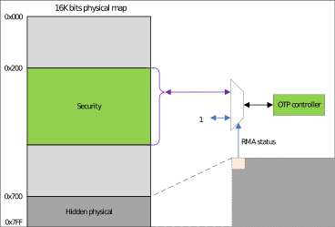
Usage by Zone
Logical Zone
The logical zone is partitioned into zones such as the system data zone, Wi-Fi calibration data zone, and user-defined MTP zone.
System Data Zone
The system data zone (0x000 ~ 0x01F, 32 bytes) is used to store system data that may be required at system boot. The system data is automatically loaded by hardware into the system registers and takes effect at system boot.
Note
Refer to the corresponding User Manual for the mapping relationship between the system data zone and the system registers.
For historical reasons, if a byte in the system data zone is programmed for the first time, the corresponding system register will retain its initial value of 0x00, rather than the 0xFF read from the logical zone. Therefore, special handling is required for the first-time programming of system data.
Note
When a byte in the system data zone has been programmed to a non-0xFF value and is then programmed back to 0xFF, the value of the corresponding system register will be 0xFF, not the initial value of 0x00. Therefore, it is not recommended to program a byte in the system data zone from a non-0xFF value to 0xFF.
System Data Programming Flow
The programming flow for system data is as follows:
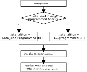
Example
To program the value of logical address 0x02[1] to 1, follow these steps:
Read the logical map to check the original value at logical address 0x02.
AT+OTP=RMAP
or
u8 data_read;
OTP_LogicalRead(&data_read, 2, 1);
Determine the value to be written based on the read value.
If the data read from logical address 0x02 in step 1 is 0xA0, it indicates that this byte is not being programmed for the first time. Perform an OR operation between 0xA0 and the target bit 0x02[1], so the new value to be written is 0xA2.
AT+OTP=WMAP,0x2,0x1,A2
or
u8 data_written = 0xA2;
OTP_LogicalWrite(2, 1, &data_written);
If the data read from logical address 0x02 in step 1 is 0xFF, it indicates that this byte is being programmed for the first time. Perform an OR operation between 0x00 and the target bit 0x02[1], so the new value to be written is 0x02.
AT+OTP=WMAP,0x2,0x1,02
or
u8 data_written = 0x02;
OTP_LogicalWrite(2, 1, &data_written);
Read the data again to verify if the write operation was successful.
AT+OTP=RMAP
or
u8 data_read;
OTP_LogicalRead(&data_read, 2, 1);
System Data Programming Scenarios
Generally, system data has its initial values, and the user modifies it as needed.
Offset |
Bit |
Symbol |
Description |
|---|---|---|---|
0x02 |
[0] |
FLASH_DEEPSLEEP_EN |
Enable Flash deep sleep mode when the system enters sleep mode. 0: Disable 1: Enable |
0x02 |
[1] |
SPIC_ADDR_4BYTE_EN |
Enable SPI Flash controller 4-byte address mode. 0: Disable 1: Enable |
0x02 |
[2] |
SPIC_BOOT_SPEEDUP_DIS |
Disable SPIC initialization speedup at boot time. 0: Speed up 1: Do not speed up |
0x02 |
[3] |
BOOT_FLASH_CLOCK_SEL |
Select Flash clock at boot time. 0: 20MHz 1: 10MHz |
0x02 |
[4] |
BOOT_INT_FLASH |
Select to boot from external or internal Flash. 0: Internal Flash 1: External Flash |
0x02 |
[5] |
BOOT_CNT_LMT_EN |
Enable soft boot count limit. 0: Disable 1: Enable |
0x02 |
[6] |
LOGIC_PQC_EN |
Enable PQC (ml-dsa-65) Check 0: Disable 1: Enable |
0x02 |
[7] |
WAKEUP_ENTRY_CHECK_EN |
Enable Wakeup Entry function Check 0: Disable 1: Enable |
0x03 |
[0] |
DIS_BOOT_LOG_EN |
Disable the boot log. 0: Enable 1: Disable |
0x03 |
[1] |
LOW_BAUD_LOG_EN |
Select Loguart baud rate. 0: 1.5Mbps 1: 115200bps |
0x03 |
[2] |
LOGIC_SECURE_BOOT_EN |
Enable Secure Boot . 0: Disable 1: Enable |
0x03 |
[3] |
LOGIC_RSIP_EN |
Enable Secure Firmware Protection (RSIP) . 0: Disable 1: Enable |
0x03 |
[4] |
LOGIC_RDP_EN |
Enable Read Protection (RDP) . 0: Disable 1: Enable |
0x03 |
[5] |
BOOT_RAND_DELAY_EN |
Enable random delay at boot time. 0: Disable 1: Enable |
0x03 |
[6] |
USB_CLK_CAL_EN |
Enable SoC clock calibration for USB. 0: Disable 1: Enable |
0x03 |
[7] |
USB_DOWNLOAD_EN |
Enable USB download function. 0: Disable 1: Enable |
0x1F |
[7] |
BOOT_VOL_SEL |
Boot voltage selection 0: 0.9v 1: 1.0v |
Offset |
Bit |
Symbol |
Description |
|---|---|---|---|
0x02 |
[0] |
FLASH_DEEPSLEEP_EN |
Enable Flash deep sleep mode when the system enters sleep mode. 0: Disable 1: Enable |
0x02 |
[1] |
SPIC_ADDR_4BYTE_EN |
Enable SPI Flash controller 4-byte address mode. 0: Disable 1: Enable |
0x02 |
[2] |
SPIC_BOOT_SPEEDUP_DIS |
Disable SPIC initialization speedup at boot time. 0: Speed up 1: Do not speed up |
0x02 |
[3] |
BOOT_FLASH_CLOCK_SEL |
Select Flash clock at boot time. 0: 20MHz 1: 10MHz |
0x03 |
[0] |
DIS_BOOT_LOG_EN |
Disable the boot log. 0: Enable 1: Disable |
0x03 |
[1] |
LOW_BAUD_LOG_EN |
Select Loguart baud rate. 0: 1.5Mbps 1: 115200bps |
0x03 |
[2] |
SECURE_BOOT_EN |
Enable Secure Boot . 0: Disable 1: Enable |
0x03 |
[3] |
RSIP_EN |
Enable Secure Firmware Protection (RSIP) . 0: Disable 1: Enable |
0x03 |
[4] |
RDP_EN |
Enable Read Protection (RDP) . 0: Disable 1: Enable |
0x03 |
[5] |
BOOT_RAND_DELAY_EN |
Enable random delay at boot time. 0: Disable 1: Enable |
0x1F |
[7] |
BOOT_VOL_SEL |
Boot voltage selection 0: 0.9v 1: 1.0v |
Offset |
Bit |
Symbol |
Description |
|---|---|---|---|
0x02 |
[0] |
FLASH_DEEPSLEEP_EN |
Enable Flash deep sleep mode when the system enters sleep mode. 0: Disable 1: Enable |
0x02 |
[1] |
SPIC_ADDR_4BYTE_EN |
Enable SPI Flash controller 4-byte address mode. 0: Disable 1: Enable |
0x02 |
[2] |
SPIC_BOOT_SPEEDUP_DIS |
Disable SPIC initialization speedup at boot time. 0: Speed up 1: Do not speed up |
0x02 |
[3] |
BOOT_FLASH_CLOCK_SEL |
Select Flash clock at boot time. 0: 20MHz 1: 10MHz |
0x03 |
[0] |
DIS_BOOT_LOG_EN |
Disable the boot log. 0: Enable 1: Disable |
0x03 |
[1] |
LOW_BAUD_LOG_EN |
Select Loguart baud rate. 0: 1.5Mbps 1: 115200bps |
0x03 |
[2] |
SECURE_BOOT_EN |
Enable Secure Boot . 0: Disable 1: Enable |
0x03 |
[3] |
RSIP_EN |
Enable Secure Firmware Protection (RSIP) . 0: Disable 1: Enable |
0x03 |
[5] |
BOOT_RAND_DELAY_EN |
Enable random delay at boot time. 0: Disable 1: Enable |
0x1F |
[7] |
BOOT_VOL_SEL |
Boot voltage selection 0: 0.9v 1: 1.0v |
Offset |
Bit |
Symbol |
Description |
|---|---|---|---|
0x02 |
[0] |
FLASH_DEEPSLEEP_EN |
Enable Flash deep sleep mode when the system enters sleep mode. 0: Disable 1: Enable |
0x02 |
[1] |
SPIC_ADDR_4BYTE_EN |
Enable SPI Flash controller 4-byte address mode. 0: Disable 1: Enable |
0x02 |
[2] |
SPIC_BOOT_SPEEDUP_DIS |
Disable SPIC initialization speedup at boot time. 0: Speed up 1: Do not speed up |
0x02 |
[3] |
BOOT_FLASH_CLOCK_SEL |
Select Flash clock at boot time. 0: 20MHz 1: 10MHz |
0x03 |
[0] |
DIS_BOOT_LOG_EN |
Disable the boot log. 0: Enable 1: Disable |
0x03 |
[1] |
LOW_BAUD_LOG_EN |
Select Loguart baud rate. 0: 1.5Mbps 1: 115200bps |
0x03 |
[2] |
SECURE_BOOT_EN |
Enable Secure Boot . 0: Disable 1: Enable |
0x03 |
[3] |
RSIP_EN |
Enable Secure Firmware Protection (RSIP) . 0: Disable 1: Enable |
0x03 |
[4] |
RDP_EN |
Enable Read Protection (RDP) . 0: Disable 1: Enable |
0x03 |
[5] |
BOOT_RAND_DELAY_EN |
Enable random delay at boot time. 0: Disable 1: Enable |
0x1F |
[7] |
BOOT_VOL_SEL |
Boot voltage selection 0: 0.9v 1: 1.0v |
Offset |
Bit |
Symbol |
Description |
|---|---|---|---|
0x02 |
[0] |
FLASH_DEEPSLEEP_EN |
Enable Flash deep sleep mode when the system enters sleep mode. 0: Disable 1: Enable |
0x02 |
[1] |
SPIC_ADDR_4BYTE_EN |
Enable SPI Flash controller 4-byte address mode. 0: Disable 1: Enable |
0x02 |
[2] |
SPIC_BOOT_SPEEDUP_DIS |
Disable SPIC initialization speedup at boot time. 0: Speed up 1: Do not speed up |
0x02 |
[3] |
BOOT_FLASH_CLOCK_SEL |
Select Flash clock at boot time. 0: 20MHz 1: 10MHz |
0x03 |
[0] |
DIS_BOOT_LOG_EN |
Disable the boot log. 0: Enable 1: Disable |
0x03 |
[1] |
LOW_BAUD_LOG_EN |
Select Loguart baud rate. 0: 1.5Mbps 1: 115200bps |
0x03 |
[2] |
SECURE_BOOT_EN |
Enable Secure Boot . 0: Disable 1: Enable |
0x03 |
[3] |
RSIP_EN |
Enable Secure Firmware Protection (RSIP) . 0: Disable 1: Enable |
0x03 |
[5] |
BOOT_RAND_DELAY_EN |
Enable random delay at boot time. 0: Disable 1: Enable |
0x1F |
[7] |
BOOT_VOL_SEL |
Boot voltage selection 0: 0.9v 1: 1.0v |
Offset |
Bit |
Symbol |
Description |
|---|---|---|---|
0x02 |
[0] |
FLASH_DEEPSLEEP_EN |
Enable Flash deep sleep mode when the system enters sleep mode. 0: Disable 1: Enable |
0x02 |
[1] |
SPIC_ADDR_4BYTE_EN |
Enable SPI Flash controller 4-byte address mode. 0: Disable 1: Enable |
0x02 |
[2] |
SPIC_BOOT_SPEEDUP_DIS |
Disable SPIC initialization speedup at boot time. 0: Speed up 1: Do not speed up |
0x02 |
[3] |
BOOT_FLASH_CLOCK_SEL |
Select Flash clock at boot time. 0: 20MHz 1: 10MHz |
0x02 |
[5:4] |
BOOT_NOR_FLASH |
Boot from Nor or Nand Flash. 0/3: Determined by power-on latch 1: Nor Flash 2: Nand Flash |
0x02 |
[6] |
USB_LOAD_SPEED |
USB speed selection in USB download mode. 0: High-speed mode 1: Full-speed mode |
0x02 |
[7] |
SPIC_NAND_PAGE_SIZE |
Nand Flash page size selection. 0: 2KB 1: 4KB |
0x03 |
[0] |
DIS_BOOT_LOG_EN |
Disable the boot log. 0: Enable log 1: Disable log |
0x03 |
[1] |
LOW_BAUD_LOG_EN |
Select Loguart baud rate. 0: 1.5Mbps 1: 115200bps |
0x03 |
[2] |
SECURE_BOOT_EN |
Enable Secure Boot . 0: Disable 1: Enable |
0x03 |
[3] |
RSIP_EN |
Enable Secure Firmware Protection (RSIP) . 0: Disable 1: Enable |
0x03 |
[4] |
RDP_EN |
Enable Read Protection (RDP) . 0: Disable 1: Enable |
0x03 |
[5] |
BOOT_RAND_DELAY_EN |
Enable random delay at boot time. 0: Disable 1: Enable |
0x03 |
[7] |
USB_DOWNLOAD_EN |
Enable USB download function. 0: Disable 1: Enable |
0x1F |
[7] |
BOOT_VOL_SEL |
Boot voltage selection 0: 0.9v 1: 1.0v |
Offset |
Bit |
Symbol |
Description |
|---|---|---|---|
0x00 |
[2:1] |
BOOT_SRC_SEL |
Select boot source. 0/3: Boot from Flash 1: Boot from USB 2: Boot from SDIO |
0x00 |
[3] |
BT_Function_EN |
Enable BT function in NIC mode. 0: Disable 1: Enable |
0x00 |
[5:4] |
SDIO_PINMUX |
Select SDIO pinmux in NIC mode. 0: PINMUX Index 0 (group 1: PA4-PA5, PA18-PA21) 1: PINMUX Index 1 (group 6: PC2-PC7) 2/3: RSVD |
0x00 |
[7:6] |
BOOT_INT_FLASH |
Boot from external or internal Flash. 0/3: Determined by power on latch 1: Internal Flash 2: External Flash |
0x02 |
[0] |
FLASH_DEEPSLEEP_EN |
Enable Flash deep sleep mode when the system enters sleep mode. 0: Disable 1: Enable |
0x02 |
[1] |
SPIC_ADDR_4BYTE_EN |
Enable SPI Flash controller 4-byte address mode. 0: Disable 1: Enable |
0x02 |
[2] |
SPIC_BOOT_SPEEDUP_DIS |
Disable SPIC initialization speedup at boot time. 0: Speed up 1: Do not speed up |
0x02 |
[3] |
BOOT_FLASH_CLOCK_SEL |
Select Flash clock at boot time. 0: 20MHz 1: 10MHz |
0x02 |
[4] |
SPIC_NAND_PAGE_SIZE |
Nand FLASH page size. 0: Auto-detect 1: 4KB |
0x02 |
[5] |
BOOT_CNT_LMT_EN |
Enable soft boot count limit. 0: Disable 1: Enable |
0x02 |
[7:6] |
BOOT_NOR_FLASH |
Boot from Nor or Nand Flash. 0/3: Determined by power-on latch 1: Nor Flash 2: Nand Flash |
0x03 |
[0] |
DIS_BOOT_LOG_EN |
Disable the boot log. 0: Enable log 1: Disable log |
0x03 |
[1] |
LOW_BAUD_LOG_EN |
Select Loguart baud rate. 0: 1.5Mbps 1: 115200bps |
0x03 |
[2] |
LOGIC_SECURE_BOOT_EN |
Enable Secure Boot . 0: Disable 1: Enable |
0x03 |
[3] |
LOGIC_RSIP_EN |
Enable Secure Firmware Protection (RSIP) . 0: Disable 1: Enable |
0x03 |
[4] |
LOGIC_RDP_EN |
Enable Read Protection (RDP) . 0: Disable 1: Enable |
0x03 |
[7] |
USB_DOWNLOAD_EN |
Enable USB download function. 0: Disable 1: Enable |
0x1F |
[7] |
BOOT_VOL_SEL |
Boot voltage selection 0: 0.9v 1: 1.0v |
Offset |
Bit |
Symbol |
Description |
|---|---|---|---|
0x00 |
[2:1] |
BOOT_SRC_SEL |
Select boot source. 0/1/3: Boot from Flash 2: Boot from SDIO |
0x00 |
[3] |
BT_Function_EN |
Enable SDIO multi-function mode (enable SDIO BT function). 0: Disable 1: Enable |
0x00 |
[5:4] |
SDIO_PINMUX |
Select SDIO pinmux in NIC mode. 0: PINMUX Index 0 (group 0: PA7-PA12) 1: PINMUX Index 1 (group 1: PA25-PA30) 2/3: RSVD |
0x00 |
[6] |
BOOT_EXT_FLASH |
Boot from internal or external Flash. 0: Internal Flash 1: External Flash |
0x02 |
[0] |
FLASH_DEEPSLEEP_EN |
Enable Flash deep sleep mode when the system enters sleep mode. 0: Disable 1: Enable |
0x02 |
[1] |
SPIC_ADDR_4BYTE_EN |
Enable SPI Flash controller 4-byte address mode. 0: Disable 1: Enable |
0x02 |
[2] |
SPIC_BOOT_SPEEDUP_DIS |
Disable SPIC initialization speedup at boot time. 0: Speed up 1: Do not speed up |
0x02 |
[3] |
BOOT_FLASH_CLOCK_SEL |
Select Flash clock at boot time. 0: 20MHz 1: 10MHz |
0x02 |
[5] |
BOOT_CNT_LMT_EN |
Enable soft boot count limit. 0: Disable 1: Enable |
0x03 |
[0] |
DIS_BOOT_LOG_EN |
Disable the boot log. 0: Enable log 1: Disable log |
0x03 |
[1] |
LOW_BAUD_LOG_EN |
Select Loguart baud rate. 0: 1.5Mbps 1: 115200bps |
0x03 |
[2] |
LOGIC_SECURE_BOOT_EN |
Enable Secure Boot . 0: Disable 1: Enable |
0x03 |
[3] |
LOGIC_RSIP_EN |
Enable Secure Firmware Protection (RSIP) . 0: Disable 1: Enable |
0x03 |
[4] |
LOGIC_RDP_EN |
Enable Read Protection (RDP) . 0: Disable 1: Enable |
0x03 |
[5] |
LOGIC_PQC_EN |
Enable PQC Secure Boot . 0: Disable 1: Enable |
0x1F |
[7] |
BOOT_VOL_SEL |
Boot voltage selection 0: 0.9v 1: 1.0v |
Offset |
Bit |
Symbol |
Description |
|---|---|---|---|
0x690 |
[0] |
FLASH_DEEP_SLEEP_DIS |
Disable Flash deep-sleep control function. 0: Enable function 1: Disable |
0x690 |
[1] |
SPIC_ADDR_4BYTE_EN |
Enable SPI Flash controller 4-byte address mode. 0: Disable 1: Enable |
0x690 |
[2] |
SPIC_BOOT_SPEEDUP_EN |
Enable SPIC boot speed-up. 0: Not speed up 1: Speed up |
0x690 |
[3] |
LOGIC_SECURE_BOOT_PQC_EN |
Enable Secure Boot PQC mode. 0: Disable 1: Enable |
0x690 |
[5:4] |
BOOT_FLASH_BAUD_SEL |
Select boot Flash baudrate. 0: 1/2 1: 1/4 2: 1/6 |
0x690 |
[7:6] |
BOOT_LOADER_LIM_EXT |
Extend boot loader SRAM space. 0: 128K + 0 (no extend) 1: 128K + 16K 2: 128K + 32K 3: 128K + 64K |
0x691 |
[1:0] |
BOOT_CORE_POWER_DELAY |
CORE power init delay option. 0: 100ms 1: 200ms 2: 300ms 3: 400ms |
0x691 |
[3:2] |
BOOT_SELECT |
Boot selection. 0/3: Boot option determined by power-on latch 1: Boot from Nor Flash 2: Boot from Nand Flash |
0x691 |
[6:4] |
BIG_PAGE_NAND |
Nand Flash page info. Bit [4]: 0: auto select (from ONFI or Page0), 1: manual Bit [5]: 0: page size 2K, 1: page size 4K (valid when bit [4] = 1) Bit [6]: 0: 64 pages/block, 1: 128 pages/block (valid when bit [4] = 1) |
0x691 |
[7] |
BOOT_WDT_SELECT[0] |
ROM boot watchdog timer enable (bit 0). BOOT_WDT_SELECT = {0x692[0], 0x691[7]}: 0/3: Enable, 8s 1: Enable, 30s 2: Disable |
0x692 |
[0] |
BOOT_WDT_SELECT[1] |
ROM boot watchdog timer enable (bit 1). See 0x691[7]. |
0x692 |
[1] |
UART_DOWNLOAD_DIS |
Disable UART download. 0: Enable 1: Disable |
0x692 |
[2] |
BOOT_LOG_DIS |
Disable the boot log. 0: Enable 1: Disable |
0x692 |
[3] |
LOW_BAUD_LOG_EN |
Select Loguart baud rate. 0: 1.5Mbps 1: 115200bps |
0x692 |
[4] |
LOGIC_SECURE_BOOT_EN |
Enable Secure Boot . 0: Disable 1: Enable |
0x692 |
[5] |
LOGIC_RSIP_EN |
Enable Secure Firmware Protection (RSIP) . 0: Disable 1: Enable |
0x692 |
[6] |
LOGIC_RDP_EN |
Enable Read Protection (RDP) . 0: Disable 1: Enable |
0x692 |
[7] |
BOOT_CNT_LMT_EN |
Enable boot count limit. 0: Disable 1: Enable |
0x693 |
[0] |
USB_DOWNLOAD_EN |
Enable USB download function. 0: Disable 1: Enable |
0x693 |
[1] |
OTP_CRC_EN |
Enable OTP CRC check. 0: Disable 1: Enable |
0x693 |
[4:2] |
RSIP_MODE |
RSIP mode. 3b’0xx: Use physical RSIP mode 3b’100 / 3b’111: XTS (mix mode) 3b’101: CTR 3b’110: GCM |
0x693 |
[5] |
ROM_NP_CLKSRC_SEL |
NP CPU clock source selection at ROM boot. 0: Low speed (xtal) 1: High speed (sys1pll) |
0x693 |
[6] |
ROM_SEC_CLKSRC_SEL |
SEC CPU clock source selection at ROM boot. 0: Low speed (xtal) 1: High speed (sys1pll) |
0x693 |
[7] |
ROM_SPIC_CLKSRC_SEL |
SPIC clock source selection at ROM boot. 0: Low speed (xtal) 1: High speed (sys1pll) |
0x694 |
[1:0] |
BOOT_CPUPLL_DELAY_RATIO |
CPUPLL init delay ratio control. 0: x1 1: x2 2: x4 |
0x694 |
[3:2] |
BOOT_SYSPLL_DELAY_RATIO |
SYS1/2PLL init delay ratio control. 0: x1 1: x2 2: x4 |
User-Defined MTP Zone
The User-defined MTP zone (0x170 ~ 0x19F, 48 bytes) can be freely used by the user.
Realtek provides dedicated APIs for this zone for user access.
API |
Description |
|---|---|
efuse_get_remaining_length |
Get the remaining available length of the mapped area. |
efuse_mtp_read |
Read all data from the User-defined MTP area. |
efuse_mtp_write |
Write data to the User-defined MTP area. |
efuse_get_remaining_length
Item |
Description |
|---|---|
Function |
Get the remaining available length of the mapped area. |
Parameters |
None |
Return Value |
Remaining available length. |
efuse_mtp_read
Item |
Description |
|---|---|
Function |
Read all data from the User-defined MTP area. |
Parameters |
|
Return Value |
Read operation result.
|
efuse_mtp_write
Item |
Description |
|---|---|
Function |
Write data to the User-defined MTP area. |
Parameters |
|
Return Value |
Write operation result.
|
API Usage
To program the value of logical address 0x172[1] (offset address 0x2) to 1, follow these steps:
Read the value from the User-defined MTP area and check the return value.
u8 data_read[48];
int ret;
ret = efuse_mtp_read(data_read);
Assume the data read from logical address 0x172 (offset address 0x2) in step 1 is 0xA0. Perform a bitwise OR operation between 0xA0 and the value for the target bit 0x172[1], keeping the other bits at their default values. Thus, the new value to be written is 0xA2.
Write the new value 0xA2 to the offset address 0x2 and check the function’s return value.
u8 data_written = 0xA2;
int ret;
ret = efuse_mtp_write(0x2, 0x1, &data_written);
Physical Zone
The physical zone is partitioned into the mapping zone, security zone, User-defined physical zone, ROM code patch zone, and hidden physical zone.
Security Zone
The security zone is divided into the following two parts:
Key area: 0x200~0x35F, 352 bytes. This area stores various types of keys and is automatically loaded into internal memory space at system boot.
Configuration area: 0x360~0x37F, 32 bytes. This area controls access permissions for the key area and other areas.
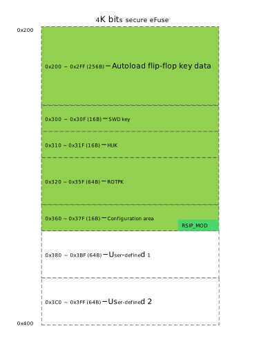
Key Area
The key area includes the following content:
Name |
Address |
Usage |
|---|---|---|
S_IPSEC_Key1 |
0x200~0x21F |
|
S_IPSEC_Key2 |
0x220~0x23F |
|
NS_IPSEC_Key1 |
0x240~0x25F |
|
NS_IPSEC_Key2 |
0x260~0x27F |
|
USER_PRI_KEY1 |
0x280~0x29F |
User private key area, free to use |
USER_PRI_KEY2 |
0x2A0~0x2BF |
|
RSIP_KEY1 |
0x2C0~0x2DF |
|
RSIP_KEY2 |
0x2E0~0x2FF |
|
SWD_PASSWORD |
0x300~0x30F |
|
HUK |
0x310~0x31F |
|
PK1 (ROTPK hash) |
0x320~0x33F |
|
PK2 (ROTPK hash) |
0x340~0x35F |
Name |
Address |
Usage |
|---|---|---|
S_IPSEC_Key1 |
0x200~0x21F |
|
S_IPSEC_Key2 |
0x220~0x23F |
|
NS_IPSEC_Key1 |
0x240~0x25F |
|
NS_IPSEC_Key2 |
0x260~0x27F |
|
ECDSA_PRI_KEY1 |
0x280~0x29F |
|
ECDSA_PRI_KEY2 |
0x2A0~0x2BF |
|
RSIP_KEY1 |
0x2C0~0x2DF |
|
RSIP_KEY2 |
0x2E0~0x2FF |
|
SWD_PASSWORD |
0x300~0x30F |
|
HUK |
0x310~0x31F |
|
PK1 (ROTPK hash) |
0x320~0x33F |
|
PK2 (ROTPK hash) |
0x340~0x35F |
Name |
Address |
Usage |
|---|---|---|
S_IPSEC_Key1 |
0x200~0x21F |
|
S_IPSEC_Key2 |
0x220~0x23F |
|
NS_IPSEC_Key1 |
0x240~0x25F |
|
NS_IPSEC_Key2 |
0x260~0x27F |
|
ECDSA_PRI_KEY1 |
0x280~0x29F |
|
ECDSA_PRI_KEY2 |
0x2A0~0x2BF |
|
RSIP_KEY1 |
0x2C0~0x2DF |
|
RSIP_KEY2 |
0x2E0~0x2FF |
|
SWD_PASSWORD |
0x300~0x30F |
|
HUK |
0x310~0x31F |
|
PK1 (ROTPK hash) |
0x320~0x33F |
|
PK2 (ROTPK hash) |
0x340~0x35F |
Name |
Address |
Usage |
|---|---|---|
S_IPSEC_Key1 |
0x200~0x21F |
|
S_IPSEC_Key2 |
0x220~0x23F |
|
NS_IPSEC_Key1 |
0x240~0x25F |
|
NS_IPSEC_Key2 |
0x260~0x27F |
|
ECDSA_PRI_KEY1 |
0x280~0x29F |
|
ECDSA_PRI_KEY2 |
0x2A0~0x2BF |
|
RSIP_KEY1 |
0x2C0~0x2DF |
|
RSIP_KEY2 |
0x2E0~0x2FF |
|
SWD_PASSWORD |
0x300~0x30F |
|
HUK |
0x310~0x31F |
|
PK1 (ROTPK hash) |
0x320~0x33F |
|
PK2 (ROTPK hash) |
0x340~0x35F |
Name |
Address |
Usage |
|---|---|---|
S_IPSEC_Key1 |
0x200~0x21F |
|
S_IPSEC_Key2 |
0x220~0x23F |
|
NS_IPSEC_Key1 |
0x240~0x25F |
|
NS_IPSEC_Key2 |
0x260~0x27F |
|
ECDSA_PRI_KEY1 |
0x280~0x29F |
|
ECDSA_PRI_KEY2 |
0x2A0~0x2BF |
|
RSIP_KEY1 |
0x2C0~0x2DF |
|
RSIP_KEY2 |
0x2E0~0x2FF |
|
SWD_PASSWORD |
0x300~0x30F |
|
HUK |
0x310~0x31F |
|
PK1 (ROTPK hash) |
0x320~0x33F |
|
PK2 (ROTPK hash) |
0x340~0x35F |
Name |
Address |
Usage |
|---|---|---|
S_IPSEC_Key1 |
0x200~0x21F |
|
S_IPSEC_Key2 |
0x220~0x23F |
|
NS_IPSEC_Key1 |
0x240~0x25F |
|
NS_IPSEC_Key2 |
0x260~0x27F |
|
ECDSA_PRI_KEY1 |
0x280~0x29F |
|
ECDSA_PRI_KEY2 |
0x2A0~0x2BF |
|
RSIP_KEY1 |
0x2C0~0x2DF |
|
RSIP_KEY2 |
0x2E0~0x2FF |
|
SWD_PASSWORD |
0x300~0x30F |
|
HUK |
0x310~0x31F |
|
PK1 (ROTPK hash) |
0x320~0x33F |
|
PK2 (ROTPK hash) |
0x340~0x35F |
Name |
Address |
Usage |
|---|---|---|
S_IPSEC_Key1 |
0x200~0x21F |
|
S_IPSEC_Key2 |
0x220~0x23F |
|
NS_IPSEC_Key1 |
0x240~0x25F |
|
NS_IPSEC_Key2 |
0x260~0x27F |
|
PKE_PRI_KEY1 |
0x280~0x29F |
|
PKE_PRI_KEY2 |
0x2A0~0x2BF |
|
RSIP_KEY1 |
0x2C0~0x2DF |
|
RSIP_KEY2 |
0x2E0~0x2FF |
|
SWD_PASSWORD |
0x300~0x30F |
|
HUK |
0x310~0x31F |
|
PK1 (ROTPK hash) |
0x320~0x33F |
|
PK2 (ROTPK hash) |
0x340~0x35F |
Name |
Address |
Usage |
|---|---|---|
S_IPSEC_Key1 |
0x200~0x21F |
|
S_IPSEC_Key2 |
0x220~0x23F |
|
NS_IPSEC_Key1 |
0x240~0x25F |
|
NS_IPSEC_Key2 |
0x260~0x27F |
|
PKE_PRI_KEY1 |
0x280~0x29F |
|
PKE_PRI_KEY2 |
0x2A0~0x2BF |
|
RSIP_KEY1 |
0x2C0~0x2DF |
|
RSIP_KEY2 |
0x2E0~0x2FF |
|
SWD_PASSWORD |
0x300~0x30F |
|
HUK |
0x310~0x31F |
|
PK1 (ROTPK hash) |
0x320~0x33F |
|
PK2 (ROTPK hash) |
0x340~0x35F |
Function |
Name |
Offset Addr |
Usage |
|---|---|---|---|
Secure IPSEC |
Secure IPSEC key 0 |
0x280~0x29F |
|
Secure IPSEC key 1 |
0x2A0~0x2BF |
||
Secure IPSEC key 2 |
0x2C0~0x2DF |
||
Secure IPSEC key 3 |
0x2E0~0x2FF |
||
Non Secure IPSEC |
Non Secure IPSEC key 0 |
0x300~0x31F |
|
Non Secure IPSEC key 1 |
0x320~0x33F |
||
PKE |
PKE Private Key 0 |
0x340~0x35F |
- |
PKE Private Key 1 |
0x360~0x37F |
||
RSIP |
RSIP ECB Key |
0x380~0x39F |
|
RSIP CTR Key |
0x3A0~0x3BF |
||
SWD |
SWD Secure Password |
0x3C0~0x3DF |
|
SWD Non Secure Password |
0x3E0~0x3FF |
||
Secure Boot |
Secure boot hash 0 |
0x400~0x41F |
|
Secure boot hash 1 |
0x420~0x43F |
||
PSA |
HUK |
0x440~0x44F |
Note
Some keys are shared by multiple features. Plan the key usage in advance to avoid conflicts.
Configuration Area
The content of the configuration area is shown in the table below. Refer to the detailed descriptions in the corresponding chapters for the specific usage of each field in this area.
Offset |
Bits |
Symbol |
Description |
Usage |
|---|---|---|---|---|
0x360 |
[31:0] |
SWD_ID |
Device’s SWD ID |
|
0x364 |
[0] |
SWD_PWD_EN |
Enable SWD password |
|
[1] |
SWD_DBGEN |
SWD external debug authentication |
||
[2] |
SWD_NIDEN |
|||
[3] |
SWD_SPIDEN |
|||
[4] |
SWD_SPNIDEN |
|||
[5] |
SWD_PWD_R_Protection_EN |
Key read and write protection enable |
||
[6] |
SWD_PWD_W_Forbidden_EN |
|||
[7] |
HUK_W_Forbidden_EN |
|||
0x365 |
[0] |
RSVD |
||
[1] |
PK1_W_Forbidden_EN |
|||
[2] |
PK2_W_Forbidden_EN |
|||
[3] |
S_IPSEC_Key1_R_Protection_EN |
|||
[4] |
S_IPSEC_Key1_W_Forbidden_EN |
|||
[5] |
S_IPSEC_Key2_R_Protection_EN |
|||
[6] |
S_IPSEC_Key2_W_Forbidden_EN |
|||
[7] |
NS_IPSEC_Key1_R_Protection_EN |
|||
0x366 |
[0] |
NS_IPSEC_Key1_W_Forbidden_EN |
||
[1] |
NS_IPSEC_Key2_R_Protection_EN |
|||
[2] |
NS_IPSEC_Key2_W_Forbidden_EN |
|||
[3] |
USER_PRI_KEY1_R_Protection_EN |
Read/write protection for user key area |
||
[4] |
USER_PRI_KEY1_W_Forbidden_EN |
|||
[5] |
USER_PRI_KEY2_R_Protection_EN |
|||
[6] |
USER_PRI_KEY2_W_Forbidden_EN |
|||
[7] |
RSIP_KEY1_R_Protection_EN |
|||
0x367 |
[0] |
RSIP_KEY1_W_Forbidden_EN |
||
[1] |
RSIP_KEY2_R_Protection_EN |
|||
[2] |
RSIP_KEY2_W_Forbidden_EN |
|||
[3] |
RSIP_MODE_W_Forbidden_EN |
|||
[4] |
SIC_SECURE_EN |
Enable/disable SIC function 1: Enable 0: Disable |
- |
|
[5] |
CPU_PC_DBG_EN |
Enable/disable allowing debug port to get CPU PC value 1: Enable 0: Disable |
- |
|
[6] |
UDF1_TRUSTZONE_EN |
User-defined 1 area (0x380~0x3BF) security protection 0: Enable 1: Disable |
- |
|
[7] |
UDF2_TRUSTZONE_EN |
User-defined 2 area (0x3C0~0x3FF) security protection 0: Enable 1: Disable |
- |
|
0x368 |
[0] |
UART_DOWNLOAD_DISABLE |
Enable/disable entering UART download mode via Trap pin 0: Disable 1: Enable |
- |
[1] |
RSVD |
- |
- |
|
[2] |
RSIP_EN |
Enable/disable RSIP function |
||
[3] |
SECURE_BOOT_EN |
Enable/disable Secure Boot function |
||
[4] |
SECURE_BOOT_HW_DIS |
|||
[5] |
RDP_EN |
Enable/disable RDP function |
||
[6] |
ANTI_ROLLBACK_EN |
|||
[7] |
FAULT_LOG_PRINT_DIS |
Enable/disable hard fault log in ROM 0: Disable 1: Enable |
- |
|
0x369 |
[1:0] |
RSIP_MODE |
RSIP mode |
|
[2] |
HUK_DERIV_EN |
Enable/disable HUK derivation |
||
[3] |
USER_PHYSICAL_TZ1_EN |
User-defined physical 1 area security protection 0: Enable 1: Disable |
- |
|
[4] |
USER_PHYSICAL_TZ2_EN |
User-defined physical 2 area security protection 0: Enable 1: Disable |
- |
|
[5] |
PQC_EN |
Enable/disable PQC (ml-dsa-65) Secure Boot |
- |
|
[6] |
SWTRIG_UART_DOWNLOAD_DISABLE |
Enable/disable entering UART download mode via software trigger 0: Disable 1: Enable |
- |
|
[7] |
SPIC_PINMUX_IN_TESTMODE_DISABLE |
For Realtek use only |
- |
|
0x36A |
[7:0] |
RSVD |
- |
- |
0x36B |
[3:0] |
SECURE_BOOT_AUTH_LOG |
Secure Boot authentication algorithm |
|
[7:4] |
SECURE_BOOT_HASH_LOG |
Secure Boot hash algorithm |
||
0x36C |
[15:0] |
OTA_ADDR |
OTA address, 4K aligned |
|
0x36E |
[15:0] |
BOOTLOADER_VERSION |
Bootloader version |
|
0x370 |
[31:0] |
CRC0 |
CRC check |
|
0x374 |
[31:0] |
CRC1 |
||
0x378 |
[31:0] |
CRC2 |
||
0x37C |
[31:0] |
CRC3 |
Offset |
Bits |
Symbol |
Description |
Usage |
|---|---|---|---|---|
0x360 |
[31:0] |
SWD_ID |
Device’s SWD ID |
|
0x364 |
[0] |
SWD_PWD_EN |
Enable SWD password |
|
[1] |
SWD_DBGEN |
SWD external debug authentication |
||
[2] |
SWD_NIDEN |
|||
[3] |
SWD_SPIDEN |
|||
[4] |
SWD_SPNIDEN |
|||
[5] |
SWD_PWD_R_Protection_EN |
Key read and write protection enable |
||
[6] |
SWD_PWD_W_Forbidden_EN |
|||
[7] |
HUK_W_Forbidden_EN |
|||
0x365 |
[0] |
RSVD |
- |
|
[1] |
PK1_W_Forbidden_EN |
|||
[2] |
PK2_W_Forbidden_EN |
|||
[3] |
S_IPSEC_Key1_R_Protection_EN |
|||
[4] |
S_IPSEC_Key1_W_Forbidden_EN |
|||
[5] |
S_IPSEC_Key2_R_Protection_EN |
|||
[6] |
S_IPSEC_Key2_W_Forbidden_EN |
|||
[7] |
NS_IPSEC_Key1_R_Protection_EN |
|||
0x366 |
[0] |
NS_IPSEC_Key1_W_Forbidden_EN |
||
[1] |
NS_IPSEC_Key2_R_Protection_EN |
|||
[2] |
NS_IPSEC_Key2_W_Forbidden_EN |
|||
[3] |
ECDSA_PRI_KEY1_R_Protection_EN |
|||
[4] |
ECDSA_PRI_KEY1_W_Forbidden_EN |
|||
[5] |
ECDSA_PRI_KEY2_R_Protection_EN |
|||
[6] |
ECDSA_PRI_KEY2_W_Forbidden_EN |
|||
[7] |
RSIP_KEY1_R_Protection_EN |
|||
0x367 |
[0] |
RSIP_KEY1_W_Forbidden_EN |
||
[1] |
RSIP_KEY2_R_Protection_EN |
|||
[2] |
RSIP_KEY2_W_Forbidden_EN |
|||
[3] |
RSIP_MODE_W_Forbidden_EN |
|||
[4] |
SIC_SECURE_EN |
Enable/disable SIC function 1: Enable 0: Disable |
- |
|
[5] |
CPU_PC_DBG_EN |
Enable/disable allowing debug port to get CPU PC value 1: Enable 0: Disable |
- |
|
[6] |
UDF1_TRUSTZONE_EN |
User-defined 1 area (0x380~0x3BF) security protection 0: Enable 1: Disable |
- |
|
[7] |
UDF2_TRUSTZONE_EN |
User-defined 2 area (0x3C0~0x3FF) security protection 0: Enable 1: Disable |
- |
|
0x368 |
[0] |
UART_DOWNLOAD_DISABLE |
Enable/disable entering UART download mode via Trap pin 0: Disable 1: Enable |
- |
[1] |
RSVD |
- |
- |
|
[2] |
RSIP_EN |
Enable/disable RSIP function |
||
[3] |
SECURE_BOOT_EN |
Enable/disable Secure Boot function |
||
[4] |
SECURE_BOOT_HW_DIS |
|||
[5] |
RDP_EN |
Enable/disable RDP function |
||
[6] |
Anti_Rollback_EN |
|||
[7] |
FAULT_LOG_PRINT_DIS |
Enable/disable hard fault log in ROM 0: Disable 1: Enable |
- |
|
0x369 |
[1:0] |
RSIP_MODE |
RSIP mode |
|
[2] |
HUK_DERIV_EN |
Enable/disable HUK derivation |
||
[3] |
USER_PHYSICAL_TZ1_EN |
User-defined physical 1 area security protection 0: Enable 1: Disable |
Program it to 0 if the User-defined physical 1 area is to be accessed only by the secure area. |
|
[4] |
USER_PHYSICAL_TZ2_EN |
User-defined physical 2 area security protection 0: Enable 1: Disable |
Program it to 0 if the User-defined physical 2 area is to be accessed only by the secure area. |
|
[5] |
SW_RSVD0 |
- |
- |
|
[6] |
SWTRIG_UART_DOWNLOAD_DISABLE |
Enable/disable entering UART download mode via software trigger 0: Disable 1: Enable |
- |
|
[7] |
SPIC_PINMUX_IN_TESTMODE_DISABLE |
For Realtek use only |
- |
|
0x36A |
[7:0] |
RSVD |
- |
- |
0x36B |
[3:0] |
SECURE_BOOT_AUTH_LOG |
Secure Boot authentication algorithm |
|
[7:4] |
SECURE_BOOT_HASH_LOG |
Secure Boot hash algorithm |
||
0x36C |
[15:0] |
OTA_ADDR |
OTA address, 4K aligned |
|
0x36E |
[15:0] |
BOOTLOADER |
Bootloader version |
|
0x370 |
[31:0] |
CRC0 |
CRC check |
|
0x374 |
[31:0] |
CRC1 |
||
0x378 |
[31:0] |
CRC2 |
||
0x37C |
[31:0] |
CRC3 |
Offset |
Bits |
Symbol |
Description |
Usage |
|---|---|---|---|---|
0x360 |
[31:0] |
SWD_ID |
Device’s SWD ID |
|
0x364 |
[0] |
SWD_PWD_EN |
Enable SWD password |
|
[1] |
SWD_DBGEN |
SWD external debug authentication |
||
[2] |
SWD_NIDEN |
|||
[3] |
SWD_SPIDEN |
|||
[4] |
SWD_SPNIDEN |
|||
[5] |
SWD_PWD_R_Protection_EN |
Key read and write protection enable |
||
[6] |
SWD_PWD_W_Forbidden_EN |
|||
[7] |
HUK_W_Forbidden_EN |
|||
0x365 |
[0] |
RSVD |
- |
|
[1] |
PK1_W_Forbidden_EN |
|||
[2] |
PK2_W_Forbidden_EN |
|||
[3] |
RSVD |
|||
[4] |
RSVD |
|||
[5] |
S_IPSEC_Key2_R_Protection_EN |
|||
[6] |
S_IPSEC_Key2_W_Forbidden_EN |
|||
[7] |
NS_IPSEC_Key1_R_Protection_EN |
|||
0x366 |
[0] |
NS_IPSEC_Key1_W_Forbidden_EN |
||
[1] |
NS_IPSEC_Key2_R_Protection_EN |
|||
[2] |
NS_IPSEC_Key2_W_Forbidden_EN |
|||
[3] |
ECDSA_PRI_KEY1_R_Protection_EN |
|||
[4] |
ECDSA_PRI_KEY1_W_Forbidden_EN |
|||
[5] |
ECDSA_PRI_KEY2_R_Protection_EN |
|||
[6] |
ECDSA_PRI_KEY2_W_Forbidden_EN |
|||
[7] |
RSIP_KEY1_R_Protection_EN |
|||
0x367 |
[0] |
RSIP_KEY1_W_Forbidden_EN |
||
[1] |
RSIP_KEY2_R_Protection_EN |
|||
[2] |
RSIP_KEY2_W_Forbidden_EN |
|||
[3] |
RSIP_MODE_W_Forbidden_EN |
|||
[4] |
SIC_SECURE_EN |
Enable/disable SIC function 1: Enable 0: Disable |
- |
|
[5] |
CPU_PC_DBG_EN |
Enable/disable allowing debug port to get CPU PC value 1: Enable 0: Disable |
- |
|
[7:6] |
RSVD |
- |
- |
|
0x368 |
[0] |
UART_DOWNLOAD_DISABLE |
Enable/disable entering UART download mode via Trap pin 0: Disable 1: Enable |
- |
[1] |
RSVD |
- |
- |
|
[2] |
RSIP_EN |
Enable/disable RSIP function |
||
[3] |
SECURE_BOOT_EN |
Enable/disable Secure Boot function |
||
[4] |
SECURE_BOOT_HW_DIS |
|||
[5] |
RSVD |
- |
- |
|
[6] |
Anti_Rollback_EN |
|||
[7] |
FAULT_LOG_PRINT_DIS |
Enable/disable hard fault log in ROM 0: Disable 1: Enable |
- |
|
0x369 |
[1:0] |
RSIP_MODE |
RSIP mode |
|
[2] |
HUK_DERIV_EN |
Enable/disable HUK derivation |
||
[3] |
SWTRIG_UART_DOWNLOAD_DISABLE |
Enable/disable entering UART download mode via software trigger 0: Disable 1: Enable |
- |
|
[7:4] |
SW_RSVD0 |
- |
- |
|
0x36A |
[7:0] |
RSVD |
- |
- |
0x36B |
[3:0] |
SECURE_BOOT_AUTH_LOG |
Secure Boot authentication algorithm |
|
[7:4] |
SECURE_BOOT_HASH_LOG |
Secure Boot hash algorithm |
||
0x36C |
[15:0] |
OTA_ADDR |
OTA address, 4K aligned |
|
0x36E |
[15:0] |
BOOTLOADER |
Bootloader version |
|
0x370 |
[31:0] |
CRC0 |
CRC check |
|
0x374 |
[31:0] |
CRC1 |
||
0x378 |
[31:0] |
CRC2 |
||
0x37C |
[31:0] |
CRC3 |
Offset |
Bits |
Symbol |
Description |
Usage |
|---|---|---|---|---|
0x360 |
[31:0] |
SWD_ID |
Device’s SWD ID |
|
0x364 |
[0] |
SWD_PWD_EN |
Enable SWD password |
|
[1] |
SWD_DBGEN |
SWD external debug authentication |
||
[2] |
SWD_NIDEN |
|||
[3] |
SWD_SPIDEN |
|||
[4] |
SWD_SPNIDEN |
|||
[5] |
SWD_PWD_R_Protection_EN |
Key read and write protection enable |
||
[6] |
SWD_PWD_W_Forbidden_EN |
|||
[7] |
HUK_W_Forbidden_EN |
|||
0x365 |
[0] |
RSVD |
- |
|
[1] |
PK1_W_Forbidden_EN |
|||
[2] |
PK2_W_Forbidden_EN |
|||
[3] |
S_IPSEC_Key1_R_Protection_EN |
|||
[4] |
S_IPSEC_Key1_W_Forbidden_EN |
|||
[5] |
S_IPSEC_Key2_R_Protection_EN |
|||
[6] |
S_IPSEC_Key2_W_Forbidden_EN |
|||
[7] |
NS_IPSEC_Key1_R_Protection_EN |
|||
0x366 |
[0] |
NS_IPSEC_Key1_W_Forbidden_EN |
||
[1] |
NS_IPSEC_Key2_R_Protection_EN |
|||
[2] |
NS_IPSEC_Key2_W_Forbidden_EN |
|||
[3] |
ECDSA_PRI_KEY1_R_Protection_EN |
|||
[4] |
ECDSA_PRI_KEY1_W_Forbidden_EN |
|||
[5] |
ECDSA_PRI_KEY2_R_Protection_EN |
|||
[6] |
ECDSA_PRI_KEY2_W_Forbidden_EN |
|||
[7] |
RSIP_KEY1_R_Protection_EN |
|||
0x367 |
[0] |
RSIP_KEY1_W_Forbidden_EN |
||
[1] |
RSIP_KEY2_R_Protection_EN |
|||
[2] |
RSIP_KEY2_W_Forbidden_EN |
|||
[3] |
RSIP_MODE_W_Forbidden_EN |
|||
[4] |
SIC_SECURE_EN |
Enable/disable SIC function 1: Enable 0: Disable |
- |
|
[5] |
CPU_PC_DBG_EN |
Enable/disable allowing debug port to get CPU PC value 1: Enable 0: Disable |
- |
|
[6] |
UDF1_TRUSTZONE_EN |
User-defined 1 area (0x380~0x3BF) security protection 0: Enable 1: Disable |
- |
|
[7] |
UDF2_TRUSTZONE_EN |
User-defined 2 area (0x3C0~0x3FF) security protection 0: Enable 1: Disable |
- |
|
0x368 |
[0] |
UART_DOWNLOAD_DISABLE |
Enable/disable entering UART download mode via Trap pin 0: Disable 1: Enable |
- |
[1] |
RSVD |
- |
- |
|
[2] |
RSIP_EN |
Enable/disable RSIP function |
||
[3] |
SECURE_BOOT_EN |
Enable/disable Secure Boot function |
||
[4] |
SECURE_BOOT_HW_DIS |
|||
[5] |
RDP_EN |
Enable/disable RDP function |
||
[6] |
Anti_Rollback_EN |
|||
[7] |
FAULT_LOG_PRINT_DIS |
Enable/disable hard fault log in ROM 0: Disable 1: Enable |
- |
|
0x369 |
[1:0] |
RSIP_MODE |
RSIP mode |
|
[2] |
HUK_DERIV_EN |
Enable/disable HUK derivation |
||
[3] |
USER_PHYSICAL_TZ1_EN |
User-defined physical 1 area security protection 0: Enable 1: Disable |
Program it to 0 if the User-defined physical 1 area is to be accessed only by the secure area. |
|
[4] |
USER_PHYSICAL_TZ2_EN |
User-defined physical 2 area security protection 0: Enable 1: Disable |
Program it to 0 if the User-defined physical 2 area is to be accessed only by the secure area. |
|
[5] |
SW_RSVD0 |
- |
- |
|
[6] |
SWTRIG_UART_DOWNLOAD_DISABLE |
Enable/disable entering UART download mode via software trigger 0: Disable 1: Enable |
- |
|
[7] |
SPIC_PINMUX_IN_TESTMODE_DISABLE |
For Realtek use only |
- |
|
0x36A |
[7:0] |
RSVD |
- |
- |
0x36B |
[3:0] |
SECURE_BOOT_AUTH_LOG |
Secure Boot authentication algorithm |
|
[7:4] |
SECURE_BOOT_HASH_LOG |
Secure Boot hash algorithm |
||
0x36C |
[15:0] |
OTA_ADDR |
OTA address, 4K aligned |
|
0x36E |
[15:0] |
BOOTLOADER |
Bootloader version |
|
0x370 |
[31:0] |
CRC0 |
CRC check |
|
0x374 |
[31:0] |
CRC1 |
||
0x378 |
[31:0] |
CRC2 |
||
0x37C |
[31:0] |
CRC3 |
Offset |
Bits |
Symbol |
Description |
Usage |
|---|---|---|---|---|
0x360 |
[31:0] |
SWD_ID |
Device’s SWD ID |
|
0x364 |
[0] |
SWD_PWD_EN |
Enable SWD password |
|
[1] |
SWD_DBGEN |
SWD external debug authentication |
||
[2] |
SWD_NIDEN |
|||
[3] |
SWD_SPIDEN |
|||
[4] |
SWD_SPNIDEN |
|||
[5] |
SWD_PWD_R_Protection_EN |
Key read and write protection enable |
||
[6] |
SWD_PWD_W_Forbidden_EN |
|||
[7] |
HUK_W_Forbidden_EN |
|||
0x365 |
[0] |
RSVD |
- |
|
[1] |
PK1_W_Forbidden_EN |
|||
[2] |
PK2_W_Forbidden_EN |
|||
[3] |
RSVD |
|||
[4] |
RSVD |
|||
[5] |
S_IPSEC_Key2_R_Protection_EN |
|||
[6] |
S_IPSEC_Key2_W_Forbidden_EN |
|||
[7] |
NS_IPSEC_Key1_R_Protection_EN |
|||
0x366 |
[0] |
NS_IPSEC_Key1_W_Forbidden_EN |
||
[1] |
NS_IPSEC_Key2_R_Protection_EN |
|||
[2] |
NS_IPSEC_Key2_W_Forbidden_EN |
|||
[3] |
ECDSA_PRI_KEY1_R_Protection_EN |
|||
[4] |
ECDSA_PRI_KEY1_W_Forbidden_EN |
|||
[5] |
ECDSA_PRI_KEY2_R_Protection_EN |
|||
[6] |
ECDSA_PRI_KEY2_W_Forbidden_EN |
|||
[7] |
RSIP_KEY1_R_Protection_EN |
|||
0x367 |
[0] |
RSIP_KEY1_W_Forbidden_EN |
||
[1] |
RSIP_KEY2_R_Protection_EN |
|||
[2] |
RSIP_KEY2_W_Forbidden_EN |
|||
[3] |
RSIP_MODE_W_Forbidden_EN |
|||
[4] |
SIC_SECURE_EN |
Enable/disable SIC function 1: Enable 0: Disable |
- |
|
[5] |
CPU_PC_DBG_EN |
Enable/disable allowing debug port to get CPU PC value 1: Enable 0: Disable |
- |
|
[7:6] |
RSVD |
- |
- |
|
0x368 |
[0] |
UART_DOWNLOAD_DISABLE |
Enable/disable entering UART download mode via Trap pin 0: Disable 1: Enable |
- |
[1] |
RSVD |
- |
- |
|
[2] |
RSIP_EN |
Enable/disable RSIP function |
||
[3] |
SECURE_BOOT_EN |
Enable/disable Secure Boot function |
||
[4] |
SECURE_BOOT_HW_DIS |
|||
[5] |
RSVD |
- |
- |
|
[6] |
Anti_Rollback_EN |
|||
[7] |
FAULT_LOG_PRINT_DIS |
Enable/disable hard fault log in ROM 0: Disable 1: Enable |
- |
|
0x369 |
[1:0] |
RSIP_MODE |
RSIP mode |
|
[2] |
HUK_DERIV_EN |
Enable/disable HUK derivation |
||
[3] |
SWTRIG_UART_DOWNLOAD_DISABLE |
Enable/disable entering UART download mode via software trigger 0: Disable 1: Enable |
- |
|
[7:4] |
SW_RSVD0 |
- |
- |
|
0x36A |
[7:0] |
RSVD |
- |
- |
0x36B |
[3:0] |
SECURE_BOOT_AUTH_LOG |
Secure Boot authentication algorithm |
|
[7:4] |
SECURE_BOOT_HASH_LOG |
Secure Boot hash algorithm |
||
0x36C |
[15:0] |
OTA_ADDR |
OTA address, 4K aligned |
|
0x36E |
[15:0] |
BOOTLOADER |
Bootloader version |
|
0x370 |
[31:0] |
CRC0 |
CRC check |
|
0x374 |
[31:0] |
CRC1 |
||
0x378 |
[31:0] |
CRC2 |
||
0x37C |
[31:0] |
CRC3 |
Offset |
Bits |
Symbol |
Description |
Usage |
|---|---|---|---|---|
0x360 |
[31:0] |
SWD_ID |
Device’s SWD ID |
|
0x364 |
[0] |
SWD_PWD_EN |
Enable SWD password |
|
[1] |
SWD_DBGEN |
SWD external debug authentication |
||
[2] |
SWD_NIDEN |
|||
[3] |
SWD_SPIDEN |
|||
[4] |
SWD_SPNIDEN |
|||
[5] |
SWD_PWD_R_Protection_EN |
Key read and write protection enable |
||
[6] |
SWD_PWD_W_Forbidden_EN |
|||
[7] |
HUK_W_Forbidden_EN |
|||
0x365 |
[0] |
RSVD |
- |
|
[1] |
PK1_W_Forbidden_EN |
|||
[2] |
PK2_W_Forbidden_EN |
|||
[3] |
S_IPSEC_Key1_R_Protection_EN |
|||
[4] |
S_IPSEC_Key1_W_Forbidden_EN |
|||
[5] |
S_IPSEC_Key2_R_Protection_EN |
|||
[6] |
S_IPSEC_Key2_W_Forbidden_EN |
|||
[7] |
NS_IPSEC_Key1_R_Protection_EN |
|||
0x366 |
[0] |
NS_IPSEC_Key1_W_Forbidden_EN |
||
[1] |
NS_IPSEC_Key2_R_Protection_EN |
|||
[2] |
NS_IPSEC_Key2_W_Forbidden_EN |
|||
[3] |
ECDSA_PRI_KEY1_R_Protection_EN |
|||
[4] |
ECDSA_PRI_KEY1_W_Forbidden_EN |
|||
[5] |
ECDSA_PRI_KEY2_R_Protection_EN |
|||
[6] |
ECDSA_PRI_KEY2_W_Forbidden_EN |
|||
[7] |
RSIP_KEY1_R_Protection_EN |
|||
0x367 |
[0] |
RSIP_KEY1_W_Forbidden_EN |
||
[1] |
RSIP_KEY2_R_Protection_EN |
|||
[2] |
RSIP_KEY2_W_Forbidden_EN |
|||
[3] |
RSIP_MODE_W_Forbidden_EN |
|||
[4] |
SIC_SECURE_EN |
Enable/disable SIC function 1: Enable 0: Disable |
- |
|
[5] |
CPU_PC_DBG_EN |
Enable/disable allowing debug port to get CPU PC value 1: Enable 0: Disable |
- |
|
[6] |
UDF1_TRUSTZONE_EN |
User-defined 1 area (0x380~0x3BF) security protection 0: Enable 1: Disable |
- |
|
[7] |
UDF2_TRUSTZONE_EN |
User-defined 2 area (0x3C0~0x3FF) security protection 0: Enable 1: Disable |
- |
|
0x368 |
[0] |
HWTRIG_UART_DOWNLOAD_DISABLE |
Enable/disable entering UART download mode via Trap pin 0: Disable 1: Enable |
- |
[1] |
RSVD |
- |
- |
|
[2] |
RSIP_EN |
Enable/disable RSIP function |
||
[3] |
SECURE_BOOT_EN |
Enable/disable Secure Boot function |
||
[4] |
SECURE_BOOT_HW_DIS |
|||
[5] |
RDP_EN |
Enable/disable RDP function |
||
[6] |
Anti_Rollback_EN |
|||
[7] |
FAULT_LOG_PRINT_DIS |
Enable/disable hard fault log in ROM 0: Disable 1: Enable |
- |
|
0x369 |
[1:0] |
RSIP_MODE |
RSIP mode |
|
[2] |
HUK_DERIV_EN |
Enable/disable HUK derivation |
||
[3] |
SWTRIG_UART_DOWNLOAD_DISABLE |
Enable/disable entering UART download mode via software trigger 0: Disable 1: Enable |
- |
|
[7:4] |
SW_RSVD0 |
- |
- |
|
0x36A |
[7:0] |
RSVD |
- |
- |
0x36B |
[3:0] |
SECURE_BOOT_AUTH_LOG |
Secure Boot authentication algorithm |
|
[7:4] |
SECURE_BOOT_HASH_LOG |
Secure Boot hash algorithm |
||
0x36C |
[15:0] |
OTA_ADDR |
OTA address, 4K aligned |
|
0x36E |
[15:0] |
BOOTLOADER_VERSION |
Bootloader version |
|
0x370 |
[31:0] |
CRC0 |
CRC check |
|
0x374 |
[31:0] |
CRC1 |
||
0x378 |
[31:0] |
CRC2 |
||
0x37C |
[31:0] |
CRC3 |
Offset |
Bits |
Symbol |
Description |
Usage |
|---|---|---|---|---|
0x360 |
[31:0] |
SWD_ID |
Device’s SWD ID |
|
0x364 |
[0] |
SWD_PWD_EN |
Enable SWD password |
|
[1] |
SWD_DBGEN |
SWD external debug authentication |
||
[2] |
SWD_NIDEN |
|||
[3] |
SWD_SPIDEN |
|||
[4] |
SWD_SPNIDEN |
|||
[5] |
SWD_PWD_R_Protection_EN |
Key read and write protection enable |
||
[6] |
SWD_PWD_W_Forbidden_EN |
|||
[7] |
HUK_W_Forbidden_EN |
|||
0x365 |
[0] |
SWD_SoftWare_CTRL_EN |
- |
|
[1] |
PK1_W_Forbidden_EN |
|||
[2] |
PK2_W_Forbidden_EN |
|||
[3] |
S_IPSEC_Key1_R_Protection_EN |
|||
[4] |
S_IPSEC_Key1_W_Forbidden_EN |
|||
[5] |
S_IPSEC_Key2_R_Protection_EN |
|||
[6] |
S_IPSEC_Key2_W_Forbidden_EN |
|||
[7] |
NS_IPSEC_Key1_R_Protection_EN |
|||
0x366 |
[0] |
NS_IPSEC_Key1_W_Forbidden_EN |
||
[1] |
NS_IPSEC_Key2_R_Protection_EN |
|||
[2] |
NS_IPSEC_Key2_W_Forbidden_EN |
|||
[3] |
PKE_PRI_KEY1_R_Protection_EN |
|||
[4] |
PKE_PRI_KEY1_W_Forbidden_EN |
|||
[5] |
PKE_PRI_KEY2_R_Protection_EN |
|||
[6] |
PKE_PRI_KEY2_W_Forbidden_EN |
|||
[7] |
RSIP_KEY1_R_Protection_EN |
|||
0x367 |
[0] |
RSIP_KEY1_W_Forbidden_EN |
||
[1] |
RSIP_KEY2_R_Protection_EN |
|||
[2] |
RSIP_KEY2_W_Forbidden_EN |
|||
[3] |
RSIP_MODE_W_Forbidden_EN |
|||
[4] |
SIC_SECURE_EN |
Enable/disable SIC function 1: Enable 0: Disable |
- |
|
[5] |
CPU_PC_DBG_EN |
Enable/disable allowing debug port to get CPU PC value 1: Enable 0: Disable |
- |
|
[6] |
UDF1_TRUSTZONE_EN |
User-defined 1 area (0x380~0x3BF) security protection 0: Enable 1: Disable |
- |
|
[7] |
UDF2_TRUSTZONE_EN |
User-defined 2 area (0x3C0~0x3FF) security protection 0: Enable 1: Disable |
- |
|
0x368 |
[0] |
UART_DOWNLOAD_DISABLE |
Enable/disable entering UART download mode via Trap pin 0: Disable 1: Enable |
- |
[1] |
RSVD |
- |
- |
|
[2] |
RSIP_EN |
Enable/disable RSIP function |
||
[3] |
SECURE_BOOT_EN |
Enable/disable Secure Boot function |
||
[4] |
BOOT_RAND_DELAY_EN |
Enable random delay on boot 0: Disable 1: Enable |
- |
|
[5] |
RDP_EN |
Enable/disable RDP function |
||
[6] |
ANTI_ROLLBACK_EN |
Enable/disable anti-rollback function |
||
[7] |
FAULT_LOG_PRINT_DIS |
Enable/disable hard fault log in ROM 0: Disable 1: Enable |
- |
|
0x369 |
[1:0] |
RSIP_MODE |
RSIP mode |
|
[2] |
HUK_DERIV_EN |
Enable/disable HUK derivation |
||
[3] |
USER_PHYSICAL_TZ1_EN |
User-defined physical 1 area security protection 0: Enable 1: Disable |
- |
|
[4] |
USER_PHYSICAL_TZ2_EN |
User-defined physical 2 area security protection 0: Enable 1: Disable |
- |
|
[5] |
PK_IDX (ROTPK hash Index) |
Public key hash index used by ROM |
Program it to 0 if PK2 is to be used. |
|
[6] |
SWTRIG_UART_DOWNLOAD_DISABLE |
Enable/disable entering UART download mode via software trigger 0: Disable 1: Enable |
- |
|
[7] |
SPIC_PG1B_DISABLE |
For mass production |
||
0x36A |
[7:0] |
RSVD |
- |
- |
0x36B |
[3:0] |
SECURE_BOOT_AUTH_LOG |
Secure Boot authentication algorithm |
|
[7:4] |
SECURE_BOOT_HASH_LOG |
Secure Boot hash algorithm |
||
0x36C |
[15:0] |
OTA_ADDR |
OTA address, 4K aligned |
|
0x370 |
[15:0] |
CRC0 |
CRC check |
|
0x372 |
[15:0] |
CRC1 |
||
0x374 |
[15:0] |
CRC2 |
||
0x376 |
[15:0] |
CRC3 |
||
0x378 |
[63:0] |
BOOTLOADER_VERSION |
Bootloader version |
Offset |
Bits |
Symbol |
Description |
Usage |
|---|---|---|---|---|
0x360 |
[31:0] |
SWD_ID |
Device’s SWD ID |
|
0x364 |
[0] |
SWD_PWD_EN |
Enable SWD password |
|
[1] |
SWD_DBGEN |
SWD external debug authentication |
||
[2] |
SWD_NIDEN |
|||
[3] |
SWD_SPIDEN |
|||
[4] |
SWD_SPNIDEN |
|||
[5] |
SWD_PWD_R_Protection_EN |
Key read and write protection enable |
||
[6] |
SWD_PWD_W_Forbidden_EN |
|||
[7] |
HUK_W_Forbidden_EN |
|||
0x365 |
[0] |
SWD_SoftWare_CTRL_EN |
- |
|
[1] |
PK1_W_Forbidden_EN |
|||
[2] |
PK2_W_Forbidden_EN |
|||
[3] |
S_IPSEC_Key1_R_Protection_EN |
|||
[4] |
S_IPSEC_Key1_W_Forbidden_EN |
|||
[5] |
S_IPSEC_Key2_R_Protection_EN |
|||
[6] |
S_IPSEC_Key2_W_Forbidden_EN |
|||
[7] |
NS_IPSEC_Key1_R_Protection_EN |
|||
0x366 |
[0] |
NS_IPSEC_Key1_W_Forbidden_EN |
||
[1] |
NS_IPSEC_Key2_R_Protection_EN |
|||
[2] |
NS_IPSEC_Key2_W_Forbidden_EN |
|||
[3] |
PKE_PRI_KEY1_R_Protection_EN |
|||
[4] |
PKE_PRI_KEY1_W_Forbidden_EN |
|||
[5] |
PKE_PRI_KEY2_R_Protection_EN |
|||
[6] |
PKE_PRI_KEY2_W_Forbidden_EN |
|||
[7] |
RSIP_KEY1_R_Protection_EN |
|||
0x367 |
[0] |
RSIP_KEY1_W_Forbidden_EN |
||
[1] |
RSIP_KEY2_R_Protection_EN |
|||
[2] |
RSIP_KEY2_W_Forbidden_EN |
|||
[3] |
RSIP_MODE_W_Forbidden_EN |
|||
[4] |
SIC_SECURE_EN |
Enable/disable SIC function 1: Enable 0: Disable |
- |
|
[5] |
CPU_PC_DBG_EN |
Enable/disable allowing debug port to get CPU PC value 1: Enable 0: Disable |
- |
|
[6] |
UDF1_TRUSTZONE_EN |
User-defined 1 area (0x380~0x3BF) security protection 0: Enable 1: Disable |
- |
|
[7] |
UDF2_TRUSTZONE_EN |
User-defined 2 area (0x3C0~0x3FF) security protection 0: Enable 1: Disable |
- |
|
0x368 |
[0] |
UART_DOWNLOAD_DISABLE |
Enable/disable entering UART download mode via Trap pin 0: Disable 1: Enable |
- |
[1] |
PQC_EN |
Enable/disable PQC Secure Boot function |
||
[2] |
RSIP_EN |
Enable/disable RSIP function |
||
[3] |
SECURE_BOOT_EN |
Enable/disable Secure Boot function |
||
[4] |
BOOT_RAND_DELAY_EN |
Enable random delay on boot 0: Disable 1: Enable |
- |
|
[5] |
RDP_EN |
Enable/disable RDP function |
||
[6] |
ANTI_ROLLBACK_EN |
Enable/disable anti-rollback function |
||
[7] |
FAULT_LOG_PRINT_DIS |
Enable/disable hard fault log in ROM 0: Disable 1: Enable |
- |
|
0x369 |
[1:0] |
RSIP_MODE |
RSIP mode |
|
[2] |
HUK_DERIV_EN |
Enable/disable HUK derivation |
||
[3] |
USER_PHYSICAL_TZ1_EN |
User-defined physical 1 area security protection 0: Enable 1: Disable |
- |
|
[4] |
USER_PHYSICAL_TZ2_EN |
User-defined physical 2 area security protection 0: Enable 1: Disable |
- |
|
[5] |
PK_IDX (ROTPK hash Index) |
Public key hash index used by ROM |
Program it to 0 if PK2 is to be used. |
|
[6] |
SWTRIG_UART_DOWNLOAD_DISABLE |
Enable/disable entering UART download mode via software trigger 0: Disable 1: Enable |
- |
|
[7] |
SPIC_PG1B_DISABLE |
For mass production |
||
0x36A |
[7:0] |
RSVD |
- |
- |
0x36B |
[3:0] |
SECURE_BOOT_AUTH_LOG |
Secure Boot authentication algorithm |
|
[7:4] |
SECURE_BOOT_HASH_LOG |
Secure Boot hash algorithm |
||
0x36C |
[15:0] |
OTA_ADDR |
OTA address, 4K aligned |
|
0x370 |
[15:0] |
CRC0 |
CRC check |
|
0x372 |
[15:0] |
CRC1 |
||
0x374 |
[15:0] |
CRC2 |
||
0x376 |
[15:0] |
CRC3 |
||
0x378 |
[63:0] |
BOOTLOADER_VERSION |
Bootloader version |
Offset Addr |
Bit |
Symbol |
Description |
Usage |
|---|---|---|---|---|
0x450 |
[7] |
SEC_IPSEC0_READ_EN |
Secure IPSEC key 0 read enable Secure IPSEC key 0 write enable Secure IPSEC key 1 read enable Secure IPSEC key 1 write enable Secure IPSEC key 2 read enable Secure IPSEC key 2 write enable Secure IPSEC key 3 read enable Secure IPSEC key 3 write enable |
|
[6] |
SEC_IPSEC0_WRITE_EN |
|||
[5] |
SEC_IPSEC1_READ_EN |
|||
[4] |
SEC_IPSEC1_WRITE_EN |
|||
[3] |
SEC_IPSEC2_READ_EN |
|||
[2] |
SEC_IPSEC2_WRITE_EN |
|||
[1] |
SEC_IPSEC3_READ_EN |
|||
[0] |
SEC_IPSEC3_WRITE_EN |
|||
0x451 |
[7] |
NON_SEC_IPSEC0_READ_EN |
Non Secure IPSEC key 0 read enable Non Secure IPSEC key 0 write enable Non Secure IPSEC key 1 read enable Non Secure IPSEC key 1 write enable |
|
[6] |
NON_SEC_IPSEC0_WRITE_EN |
|||
[5] |
NON_SEC_IPSEC1_READ_EN |
|||
[4] |
NON_SEC_IPSEC1_WRITE_EN |
|||
[3] |
PKE0_READ_EN |
PKE private key 0 read enable PKE private key 0 write enable PKE private key 1 read enable PKE private key 1 write enable |
- |
|
[2] |
PKE0_WRITE_EN |
|||
[1] |
PKE1_READ_EN |
|||
[0] |
PKE1_WRITE_EN |
|||
0x452 |
[7] |
RSIP_ECB_READ_EN |
RSIP ECB Key read enable RSIP ECB Key write enable RSIP CTR Key read enable RSIP CTR Key write enable |
|
[6] |
RSIP_ECB_WRITE_EN |
|||
[5] |
RSIP_CTR_READ_EN |
|||
[4] |
RSIP_CTR_WRITE_EN |
|||
[3] |
SEC_HASH0_WRITE_EN |
Secure boot hash 0 write enable Secure boot hash 1 write enable |
||
[2] |
SEC_HASH1_WRITE_EN |
|||
[1] |
HUK_WRITE_EN |
HUK write enable |
||
[0] |
RSIP_MODE_WRITE_EN |
RSIP mode write enable |
||
0x453 |
[7] |
SWD_SEC_READ_EN |
SWD Secure Password read enable SWD Secure Password write enable SWD Non Secure Password read enable SWD Non Secure Password write enable |
|
[6] |
SWD_SEC_WRITE_EN |
|||
[5] |
SWD_NON_SEC_READ_EN |
|||
[4] |
SWD_NON_SEC_WRITE_EN |
|||
[3:0] |
DUMMY_453 |
- |
- |
|
0x454 |
[7] |
SIC_SEC_EN |
SIC secure enable AON OTP access enable - |
- |
[6] |
AON_OTP_EN |
|||
[5:0] |
DUMMY_454 |
|||
0x455 |
[7] |
RSIP_MODE_0 |
RSIP Mode bit 0 RSIP Mode bit 1 |
|
[6] |
RSIP_MODE_1 |
|||
[5:0] |
SW_RSVD |
- |
- |
|
0x456 |
[7] |
RSIP_DISABLE |
RSIP disable |
|
[6] |
SEC_BOOT_DIS |
Secure boot disable Secure boot ECC select Secure boot random delay disable |
||
[5] |
SEC_BOOT_ECC_SEL |
|||
[4] |
SEC_BOOT_RANDM_DLY_DIS |
|||
[3] |
RDP_DIS |
RDP disable |
||
[2] |
ANTIROLL_BACK_DIS |
Anti roll back disable |
||
[1] |
HW_UART_DWLD_EN |
Hardware UART download disable Software UART download disable |
- |
|
[0] |
SW_UART_DWLD_EN |
|||
0x457 |
[7] |
FAULT_LOG_EN |
Fault log disable HUK derive disable |
- |
[6] |
HUK_DERV_DIS |
|||
[5] |
SEC_BOOT_HASH_IDX |
Secure boot hash index |
||
[4] |
SWD_FIXED_KEY_EN |
SWD fixed key enable Secure SWD Mode Select 0 Secure SWD Mode Select 1 Non Secure SWD Mode Select 0 Non Secure SWD Mode Select 1 |
||
[3] |
SEC_SWD_MODE_SEL0 |
|||
[2] |
SEC_SWD_MODE_SEL1 |
|||
[1] |
NON_SEC_SWD_MODE_SEL0 |
|||
[0] |
NON_SEC_SWD_MODE_SEL1 |
|||
0x458 |
[7:4] |
SEC_BOOT_AUTH_ALG[3:0] |
Secure boot authentication algorithm Secure boot hash algorithm |
|
[3:0] |
SEC_BOOT_HASH_ALG[3:0] |
|||
0x459~0x45D |
[7:0] |
SW_RSVD |
- |
- |
0x45E |
[7:0] |
OTA_ADDR_0 |
OTA address byte 0 OTA address byte 1 |
|
0x45F |
[7:0] |
OTA_ADDR_1 |
||
0x460~0x46F |
[7:0] |
BL_VER_0~F |
Bootloader version 0~15 |
Note
If RSIP_MODE_W_Forbidden_EN is programmed, then 0x369[7:0] cannot be programmed
Security Zone CRC Check
CRC is used to defend against injection attacks. Protection is achieved by comparing a valid CRC entry programmed into the OTP with the CRC value calculated by the hardware for the security zone, ensuring that the security zone has not been attacked.
CRC Entry Usage Rules
There are 4 CRC entries in total in the OTP, each including 2 bytes of magic number and 2 bytes of valid CRC value. Only one entry can be used at a time, and they must be used in sequence. The current security zone CRC value can be obtained through hardware without software calculation. When enabling a new entry, program all previously used entries to 0x00 to invalidate them. These operations are integrated into the
OTP_SetCRC()function, which users only need to call.The CRC calculation range is the security zone part (0x200~0x36B).
Ensure the security zone programming is completed before programming the CRC entry. Any modification to the calculation range in the security zone will change the CRC value, requiring reprogramming of a new CRC entry.
Once CRC checking is enabled, it cannot be disabled. If the magic number or valid CRC check fails, the ROM will enter an infinite loop.
CRC Entry Usage Rules
There are 4 CRC entries in total in the OTP, each including 2 bytes of magic number and 2 bytes of valid CRC value. Only one entry can be used at a time, and they must be used in sequence. The current security zone CRC value can be obtained through hardware without software calculation. When enabling a new entry, program all previously used entries to 0x00 to invalidate them. These operations are integrated into the
OTP_SetCRC()function, which users only need to call.The CRC calculation range is the security zone part (0x200~0x36B).
Ensure the security zone programming is completed before programming the CRC entry. Any modification to the calculation range in the security zone will change the CRC value, requiring reprogramming of a new CRC entry.
Once CRC checking is enabled, it cannot be disabled. If the magic number or valid CRC check fails, the ROM will enter an infinite loop.
CRC Entry Usage Rules
There are 4 CRC entries in total in the OTP, each including 2 bytes of magic number and 2 bytes of valid CRC value. Only one entry can be used at a time, and they must be used in sequence. The current security zone CRC value can be obtained through hardware without software calculation. When enabling a new entry, program all previously used entries to 0x00 to invalidate them. These operations are integrated into the
OTP_SetCRC()function, which users only need to call.The CRC calculation range is the security zone part (0x200~0x36B).
Ensure the security zone programming is completed before programming the CRC entry. Any modification to the calculation range in the security zone will change the CRC value, requiring reprogramming of a new CRC entry.
Once CRC checking is enabled, it cannot be disabled. If the magic number or valid CRC check fails, the ROM will enter an infinite loop.
CRC Entry Usage Rules
There are 4 CRC entries in total in the OTP, each including 2 bytes of magic number and 2 bytes of valid CRC value. Only one entry can be used at a time, and they must be used in sequence. The current security zone CRC value can be obtained through hardware without software calculation. When enabling a new entry, program all previously used entries to 0x00 to invalidate them. These operations are integrated into the
OTP_SetCRC()function, which users only need to call.The CRC calculation range is the security zone part (0x200~0x36B).
Ensure the security zone programming is completed before programming the CRC entry. Any modification to the calculation range in the security zone will change the CRC value, requiring reprogramming of a new CRC entry.
Once CRC checking is enabled, it cannot be disabled. If the magic number or valid CRC check fails, the ROM will enter an infinite loop.
CRC Entry Usage Rules
There are 4 CRC entries in total in the OTP, each including 2 bytes of magic number and 2 bytes of valid CRC value. Only one entry can be used at a time, and they must be used in sequence. The current security zone CRC value can be obtained through hardware without software calculation. When enabling a new entry, program all previously used entries to 0x00 to invalidate them. These operations are integrated into the
OTP_SetCRC()function, which users only need to call.The CRC calculation range is the security zone part (0x200~0x36B).
Ensure the security zone programming is completed before programming the CRC entry. Any modification to the calculation range in the security zone will change the CRC value, requiring reprogramming of a new CRC entry.
Once CRC checking is enabled, it cannot be disabled. If the magic number or valid CRC check fails, the ROM will enter an infinite loop.
CRC Entry Usage Rules
There are 4 CRC entries in total in the OTP, each including 2 bytes of magic number and 2 bytes of valid CRC value. Only one entry can be used at a time, and they must be used in sequence. The current security zone CRC value can be obtained through hardware without software calculation. When enabling a new entry, program all previously used entries to 0x00 to invalidate them. These operations are integrated into the
OTP_SetCRC()function, which users only need to call.The CRC calculation range is the security zone part (0x200~0x36B).
Ensure the security zone programming is completed before programming the CRC entry. Any modification to the calculation range in the security zone will change the CRC value, requiring reprogramming of a new CRC entry.
Once CRC checking is enabled, it cannot be disabled. If the magic number or valid CRC check fails, the ROM will enter an infinite loop.
CRC Entry Usage Rules
The physical OTP contains a total of 4 CRC entries, with each entry containing 2 bytes of valid CRC value. Only one entry can be used at a time, and they must be used in sequence. The CRC value of the current security zone can be obtained through hardware without software calculation. These operations are integrated into the
OTP_SetCRC()function, and users only need to call this function.The CRC calculation range is the security zone (0x200~0x36F) portion.
Ensure that the security zone programming is completed before programming the CRC entry. Any modification to the calculation range of the security zone will result in a change of the CRC value, requiring reprogramming of a new CRC entry.
Once the CRC check is enabled, it cannot be disabled. If the CRC check fails, the ROM will enter an infinite loop.
CRC Entry Usage Rules
The physical OTP contains a total of 4 CRC entries, with each entry containing 2 bytes of valid CRC value. Only one entry can be used at a time, and they must be used in sequence. The CRC value of the current security zone can be obtained through hardware without software calculation. These operations are integrated into the
OTP_SetCRC()function, and users only need to call this function.The CRC calculation range is the security zone (0x200~0x36F) portion.
Ensure that the security zone programming is completed before programming the CRC entry. Any modification to the calculation range of the security zone will result in a change of the CRC value, requiring reprogramming of a new CRC entry.
Once the CRC check is enabled, it cannot be disabled. If the CRC check fails, the ROM will enter an infinite loop.
CRC Entry Layout
Each key area has an independent 2-byte CRC entry at the following physical addresses:
Offset Addr |
Content |
Size (Byte) |
|---|---|---|
0x560 |
CRC for Secure IPSEC key 0 |
2 |
0x562 |
CRC for Secure IPSEC key 1 |
2 |
0x564 |
CRC for Secure IPSEC key 2 |
2 |
0x566 |
CRC for Secure IPSEC key 3 |
2 |
0x568 |
CRC for Non Secure IPSEC key 0 |
2 |
0x56A |
CRC for Non Secure IPSEC key 1 |
2 |
0x56C |
CRC for PKE Private Key 0 |
2 |
0x56E |
CRC for PKE Private Key 1 |
2 |
0x570 |
CRC for RSIP ECB Key |
2 |
0x572 |
CRC for RSIP CTR Key |
2 |
0x574 |
CRC for SWD Secure Password |
2 |
0x576 |
CRC for SWD Non Secure Password |
2 |
0x578 |
CRC for Secure boot hash 0 |
2 |
0x57A |
CRC for Secure boot hash 1 |
2 |
0x57C |
CRC for HUK |
2 |
0x57E |
CRC for 0x450~0x45F |
2 |
0x580 |
CRC for RMA SWD Secure Password |
2 |
0x582 |
CRC for RMA SWD Non Secure Password |
2 |
0x584 |
CRC for RMA boot hash |
2 |
0x586 |
RSVD |
2 |
Example
Ensure the security zone has been modified.
Write the CRC value and determine if the write was successful based on the return value and printed information.
int ret;
ret = OTP_SetCRC();
Restart the chip.
If the CRC entry check passes, the boot process will proceed successfully.
If the CRC entry check fails, the chip will enter an infinite loop in ROM and fail to boot normally.
Caution
It is recommended that users enable this function only when there is a need to defend against injection attacks. Otherwise, once this function is enabled, if the security zone CRC value does not match the value written to the CRC entry, the chip will be permanently unable to boot.
If the CRC entry has already been programmed and the user needs to modify the security zone again, the new CRC value must be written before rebooting. Otherwise, the chip will be permanently unable to boot.
User-Defined Physical Zone
There are 4 blocks in the user-defined zone, which can be used freely by the user.
Name |
Zone |
Usage Method |
|---|---|---|
User_defined1 |
0x380-0x3BF |
|
User_defined2 |
0x3C0-0x3FF |
|
User_physical1 |
0x400-0x480 |
|
User_physical2 |
0x480-0x4FF |
|
Name |
Zone |
Usage Method |
|---|---|---|
User_defined1 |
0x380-0x3BF |
|
User_defined2 |
0x3C0-0x3FF |
|
User_physical1 |
0x400-0x480 |
|
User_physical2 |
0x480-0x4FF |
|
Name |
Zone |
Usage Method |
|---|---|---|
User_defined1 |
0x380-0x3BF |
|
User_defined2 |
0x3C0-0x3FF |
|
User_physical1 |
0x400-0x480 |
Free for user use. |
User_physical2 |
0x480-0x4FF |
Free for user use. |
Name |
Zone |
Usage Method |
|---|---|---|
User_defined1 |
0x380-0x3BF |
|
User_defined2 |
0x3C0-0x3FF |
|
User_physical1 |
0x400-0x480 |
|
User_physical2 |
0x480-0x4FF |
|
Name |
Zone |
Usage Method |
|---|---|---|
User_defined1 |
0x380-0x3BF |
|
User_defined2 |
0x3C0-0x3FF |
|
User_physical1 |
0x400-0x480 |
Free for user use. |
User_physical2 |
0x480-0x4FF |
Free for user use. |
Name |
Zone |
Usage Method |
|---|---|---|
User_defined1 |
0x380-0x3BF |
|
User_defined2 |
0x3C0-0x3FF |
|
User_physical1 |
0x400-0x480 |
|
User_physical2 |
0x480-0x4FF |
|
Name |
Zone |
Usage Method |
|---|---|---|
User_defined1 |
0x380-0x3BF |
|
User_defined2 |
0x3C0-0x3FF |
|
User_physical1 |
0x400-0x480 |
|
User_physical2 |
0x480-0x4FF |
|
Name |
Zone |
Usage Method |
|---|---|---|
User_defined1 |
0x380-0x3BF |
|
User_defined2 |
0x3C0-0x3FF |
|
User_physical1 |
0x400-0x480 |
|
User_physical2 |
0x480-0x4FF |
|
Name |
Zone |
Usage Method |
|---|---|---|
User_defined1 |
0x4E0-0x55F |
|
Realtek provides dedicated APIs for this zone for user access.
API |
Description |
|---|---|
efuse_otp_read |
Read data from User-defined physical zone |
efuse_otp_write |
Write data to User-defined physical zone |
efuse_otp_read
Item |
Description |
|---|---|
Function |
Read data from User-defined physical zone |
Parameters |
|
Return Value |
Read operation result
|
efuse_otp_write
Item |
Description |
|---|---|
Function |
Write data to User-defined physical zone |
Parameters |
|
Return Value |
Write operation result
|
API Usage
To program physical address 0x382[1] (offset address: 0x2) to 0, follow these steps:
Read value and check return value.
u8 data_read;
int ret;
ret = efuse_otp_read(0x2, 0x1, &data_read);
Assume the read data from step 1 is 0xAF. Perform AND operation on 0xAF with target bit 0x382[1] value while keeping other bits default. The new value becomes 0xAD.
Write new value 0xAD to physical address 0x02 and check return value.
u8 data_written = 0xAD;
int ret;
ret = efuse_otp_write(0x2, 0x1, &data_written);
ROM Code Patch Zone
The ROM code patch zone (0x500 ~ 0x6FF, 512 bytes) is used for adding patches to the ROM within certain limits.
Note
If the ROM code patch feature is enabled, after write protection is enabled for the corresponding zone, it has the same level of security as a mask ROM.
At the time of chip manufacturing, if the ROM code patch feature is not enabled,
ROM_PATCH_ENwill be programmed to 0, permanently disabling this feature.Realtek does not currently use this zone. It can be used as a user-defined zone. Please consult Realtek for the methods and precautions for using this zone.
This zone is divided into multiple parts, and each part has an independent control bit.
Offset |
Bit |
Symbol |
Description |
|---|---|---|---|
0x701 |
[1:0] |
ROM_PATCH_EN |
Enable ROM code patch function 1/2: Enable 0/3: Disable |
[2] |
ROM_PATCH_LWE1 |
Enable write protection for ROM code patch area (0x500 ~ 0x51F, 32 bytes) 0: Enable 1: Disable |
|
[3] |
ROM_PATCH_LWE2 |
Enable write protection for ROM code patch area (0x520 ~ 0x53F, 32 bytes) 0: Enable 1: Disable |
|
[4] |
ROM_PATCH_LWE3 |
Enable write protection for ROM code patch area (0x540 ~ 0x55F, 32 bytes) 0: Enable 1: Disable |
|
[5] |
ROM_PATCH_LWE4 |
Enable write protection for ROM code patch area (0x560 ~ 0x57F, 32 bytes) 0: Enable 1: Disable |
|
[6] |
ROM_PATCH_LWE5 |
Enable write protection for ROM code patch area (0x580 ~ 0x5FF, 128 bytes) 0: Enable 1: Disable |
|
[7] |
ROM_PATCH_HWE |
Enable write protection for ROM code patch area (0x600 ~ 0x6FF, 256 bytes) 0: Enable 1: Disable |
Offset |
Bit |
Symbol |
Description |
|---|---|---|---|
0x701 |
[1:0] |
ROM_PATCH_EN |
Enable ROM code patch function 1/2: Enable 0/3: Disable |
[2] |
ROM_PATCH_LWE1 |
Enable write protection for ROM code patch area (0x500 ~ 0x5FF, 256 bytes) 0: Enable 1: Disable |
|
[7] |
ROM_PATCH_HWE |
Enable write protection for ROM code patch area (0x600 ~ 0x6FF, 256 bytes) 0: Enable 1: Disable |
Offset |
Bit |
Symbol |
Description |
|---|---|---|---|
0x701 |
[1:0] |
ROM_PATCH_EN |
Enable ROM code patch function 1/2: Enable 0/3: Disable |
[2] |
ROM_PATCH_LWE1 |
Enable write protection for ROM code patch area (0x500 ~ 0x5FF, 256 bytes) 0: Enable 1: Disable |
|
[7] |
ROM_PATCH_HWE |
Enable write protection for ROM code patch area (0x600 ~ 0x6FF, 256 bytes) 0: Enable 1: Disable |
Offset |
Bit |
Symbol |
Description |
|---|---|---|---|
0x701 |
[1:0] |
ROM_PATCH_EN |
Enable ROM code patch function 1/2: Enable 0/3: Disable |
[2] |
ROM_PATCH_LWE1 |
Enable write protection for ROM code patch area (0x500 ~ 0x5FF, 256 bytes) 0: Enable 1: Disable |
|
[7] |
ROM_PATCH_HWE |
Enable write protection for ROM code patch area (0x600 ~ 0x6FF, 256 bytes) 0: Enable 1: Disable |
Offset |
Bit |
Symbol |
Description |
|---|---|---|---|
0x701 |
[1:0] |
ROM_PATCH_EN |
Enable ROM code patch function 1/2: Enable 0/3: Disable |
[2] |
ROM_PATCH_LWE1 |
Enable write protection for ROM code patch area (0x500 ~ 0x5FF, 256 bytes) 0: Enable 1: Disable |
|
[7] |
ROM_PATCH_HWE |
Enable write protection for ROM code patch area (0x600 ~ 0x6FF, 256 bytes) 0: Enable 1: Disable |
Offset |
Bit |
Symbol |
Description |
|---|---|---|---|
0x701 |
[1:0] |
ROM_PATCH_EN |
Enable ROM code patch function 1/2: Enable 0/3: Disable |
[2] |
ROM_PATCH_LWE1 |
Enable write protection for ROM code patch area (0x500 ~ 0x5FF, 256 bytes) 0: Enable 1: Disable |
|
[7] |
ROM_PATCH_HWE |
Enable write protection for ROM code patch area (0x600 ~ 0x6FF, 256 bytes) 0: Enable 1: Disable |
Offset |
Bit |
Symbol |
Description |
|---|---|---|---|
0x701 |
[1:0] |
ROM_PATCH_EN |
Enable ROM code patch function 1/2: Enable 0/3: Disable |
[2] |
ROM_PATCH_LWE1 |
Enable write protection for ROM code patch area (0x500 ~ 0x51F, 32 bytes) 0: Enable 1: Disable |
|
[3] |
ROM_PATCH_LWE2 |
Enable write protection for ROM code patch area (0x520 ~ 0x53F, 32 bytes) 0: Enable 1: Disable |
|
[4] |
ROM_PATCH_LWE3 |
Enable write protection for ROM code patch area (0x540 ~ 0x55F, 32 bytes) 0: Enable 1: Disable |
|
[5] |
ROM_PATCH_LWE4 |
Enable write protection for ROM code patch area (0x560 ~ 0x57F, 32 bytes) 0: Enable 1: Disable |
|
[6] |
ROM_PATCH_LWE5 |
Enable write protection for ROM code patch area (0x580 ~ 0x5FF, 128 bytes) 0: Enable 1: Disable |
|
[7] |
ROM_PATCH_HWE |
Enable write protection for ROM code patch area (0x600 ~ 0x6FF, 256 bytes) 0: Enable 1: Disable |
Offset |
Bit |
Symbol |
Description |
|---|---|---|---|
0x701 |
[1:0] |
ROM_PATCH_EN |
Enable ROM code patch function 1/2: Enable 0/3: Disable |
[2] |
ROM_PATCH_LWE1 |
Enable write protection for ROM code patch area (0x500 ~ 0x51F, 32 bytes) 0: Enable 1: Disable |
|
[3] |
ROM_PATCH_LWE2 |
Enable write protection for ROM code patch area (0x520 ~ 0x53F, 32 bytes) 0: Enable 1: Disable |
|
[4] |
ROM_PATCH_LWE3 |
Enable write protection for ROM code patch area (0x540 ~ 0x55F, 32 bytes) 0: Enable 1: Disable |
|
[5] |
ROM_PATCH_LWE4 |
Enable write protection for ROM code patch area (0x560 ~ 0x57F, 32 bytes) 0: Enable 1: Disable |
|
[6] |
ROM_PATCH_LWE5 |
Enable write protection for ROM code patch area (0x580 ~ 0x5FF, 128 bytes) 0: Enable 1: Disable |
|
[7] |
ROM_PATCH_HWE |
Enable write protection for ROM code patch area (0x600 ~ 0x6FF, 256 bytes) 0: Enable 1: Disable |
This feature is not supported.