Temperature Sensor
Introduction
The thermal sensor of the chip is used to monitor the temperature inside the chip, and provide low-temperature warning, high-temperature warning and over-temperature protection.
When the temperature exceeds the limit high-temperature threshold, an interrupt will be sent to the CPU, and the CPU can reduce the frequency.
When the temperature exceeds the limit low-temperature threshold, an interrupt will be sent to the CPU, and the CPU can increase the frequency.
When the temperature exceeds the limit over-temperature protection threshold, the hardware will automatically power down for over-temperature protection.
Features
No calibration
Measurement range: -40°C ~ 125°C
Variation: ±1.5°C (typical), ±5°C (worst case)
Resolution: 0.0125°C
Clock: 2MHz
19-bit thermal temperature value: 1 signed bit, 8 integer bits, and 10 decimal bits
Provides low-temperature warning, high-temperature warning and over-temperature protection
Provides access protection for thermal enable bit and over-temperature enable bit
Measurement range: ─40°C ~ 125°C
Variation: ±5°C (typical), ±10°C (worst)
Provides low- temperature warning, high-temperature warning and over-temperature protection
Provides thermal enable and over-temperature protection enable write access control
Block Diagram
The thermal block diagram is shown in the following figure.

The thermal module includes the following sub-modules:
Bias circuit
Generates bias current for bipolar core.
Bipolar core
Generates temperature-dependent voltages ΔV_BE and V_BE.
∑-∆ ADC
Contains a ∑-∆ modulator and a decimation filter.
Outputs a temperature-dependent digital value.
Controller
Controls and manages the interrupts.
Controls low-temperature warning, high-temperature warning, and over-temperature protection.
Register
Contains configuration registers, result registers, and interrupt registers.
Provides the interface to software.
Allows the measured temperature to be read directly from the registers.
Bipolar Core
To produce a digital temperature reading, a ratio-metric measurement has to be performed: a temperature-dependent signal has to be compared to a reference signal.
While virtually every device has temperature-dependent characteristics, two diode-connected substrate PNP transistors are used to generate two voltages: one with a negative temperature coefficient (V_BE) and one with a positive temperature coefficient (ΔV_BE). They can be used to generate both a voltage that is accurately proportional to absolute temperature (PTAT), and a temperature-independent bandgap reference voltage.
The block diagram of the substrate PNP transistors is shown in the following figure.

The relationship between temperature, V_BE, and ΔV_BE is shown in the following figure.

μ = (α * ΔV_BE) / (V_BE + α * ΔV_BE) = V_PTAT / V_REF
V_PTAT = α * ΔV_BE, which is proportional to absolute temperature.
V_REF = V_BE + α * ΔV_BE, which is a conventional bandgap reference voltage (around 1.2V), with a zero temperature coefficient.
μ is proportional to temperature; α should be chosen reasonably to achieve the target V_REF.
∑-∆ ADC
The ∑-∆ ADC contains a ∑-∆ modulator and a decimation filter. V_BE and ΔV_BE are input to a ∑-∆ modulator, which produces a bitstream bs, of which the average value μ is equal to the ratio of α * ΔV_BE and V_REF. A decimation filter is used to filter the quantization noise from the bitstream bs and perform the required scaling to obtain the ADC output Dout.
The block diagram of the ∑-∆ modulator is shown in the following figure.
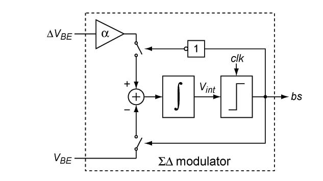
The ∑-∆ modulator consists of a loop filter and a clocked comparator. For simplicity, only a first-order loop filter is shown. In the actual modulator, a second-order filter is used. Every clock cycle, the comparator produces a bit of the bitstream bs based on the polarity of the output Vint of the loop filter. The feedback is arranged to drive the output of the integrator to zero.
If the bitstream in a given clock cycle is zero, α * ΔV_BE is integrated, while -V_BE is integrated if the bitstream is one. This can be expressed as follows:

As a result of the feedback in the modulator, the average input to the integrator is zero. In other words, the charge added by α * ΔV_BE is balanced by the charge removed by -V_BE.

So ∑-∆ modulator realizes the quantization of μ.
The thermal block diagram is shown in the following figure.
The thermal module includes the following sub-modules:
Bias circuit
Generates bias current for bipolar core.
Bipolar core
Generates temperature-dependent voltages ΔV_BE and V_BE.
∑-∆ ADC
Contains a ∑-∆ modulator and a decimation filter.
Outputs a temperature-dependent digital value.
Controller
Controls and manages the interrupts.
Controls low-temperature warning, high-temperature warning, and over-temperature protection.
Register
Contains configuration registers, result registers, and interrupt registers.
Provides the interface to software.
Allows the measured temperature to be read directly from the registers.
Bipolar Core
To produce a digital temperature reading, a ratio-metric measurement has to be performed: a temperature-dependent signal has to be compared to a reference signal.
While virtually every device has temperature-dependent characteristics, two diode-connected substrate PNP transistors are used to generate two voltages: one with a negative temperature coefficient (V_BE) and one with a positive temperature coefficient (ΔV_BE). They can be used to generate both a voltage that is accurately proportional to absolute temperature (PTAT), and a temperature-independent bandgap reference voltage.
The block diagram of the substrate PNP transistors is shown in the following figure.
The relationship between temperature, V_BE, and ΔV_BE is shown in the following figure.
μ = (α * ΔV_BE) / (V_BE + α * ΔV_BE) = V_PTAT / V_REF
V_PTAT = α * ΔV_BE, which is proportional to absolute temperature.
V_REF = V_BE + α * ΔV_BE, which is a conventional bandgap reference voltage (around 1.2V), with a zero temperature coefficient.
μ is proportional to temperature; α should be chosen reasonably to achieve the target V_REF.
∑-∆ ADC
The ∑-∆ ADC contains a ∑-∆ modulator and a decimation filter. V_BE and ΔV_BE are input to a ∑-∆ modulator, which produces a bitstream bs, of which the average value μ is equal to the ratio of α * ΔV_BE and V_REF. A decimation filter is used to filter the quantization noise from the bitstream bs and perform the required scaling to obtain the ADC output Dout.
The block diagram of the ∑-∆ modulator is shown in the following figure.
The ∑-∆ modulator consists of a loop filter and a clocked comparator. For simplicity, only a first-order loop filter is shown. In the actual modulator, a second-order filter is used. Every clock cycle, the comparator produces a bit of the bitstream bs based on the polarity of the output Vint of the loop filter. The feedback is arranged to drive the output of the integrator to zero.
If the bitstream in a given clock cycle is zero, α * ΔV_BE is integrated, while -V_BE is integrated if the bitstream is one. This can be expressed as follows:
As a result of the feedback in the modulator, the average input to the integrator is zero. In other words, the charge added by α * ΔV_BE is balanced by the charge removed by -V_BE.
So ∑-∆ modulator realizes the quantization of μ.
The following figure shows the block diagram of the thermal and SAR ADC.
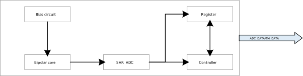
The thermal includes the following sub-modules:
Bias circuit
Generates bias current for bipolar core
Bipolar core
Generates temperature-dependent voltages
SAR ADC
12bits SAR ADC convert to 12 bits ADC code
Thermal is ch8 of SAR ADC
Controller
Controls and manages the interrupt
Controls low- temperature warning, high-temperature warning and over-temperature protection
Register
Contains configuration registers, result registers, interrupt registers
The interface to software
Functional Description
Operation Flow
The operation flow of the thermal sensor is shown in the following figure.

The operation flow is mainly divided into an initialization phase and a continuous monitoring phase. The system continuously compares the sensor output temperature ( TM_OUT ) with three predefined thresholds to adopt different software and hardware protection mechanisms. The specific flow is as follows:
Initialization Phase
After the system starts, it first enters the initialization flow. During this phase, the system executes the following operations sequentially:
Configure the relevant parameters of the Analog-to-Digital Converter (ADC).
Set temperature thresholds and enable the threshold comparison function. The temperature threshold is a two’s complement value corresponding to the Celsius temperature (1 sign bit + 8 integer bits); for example, the threshold for 125°C is 0x7D, and the threshold for -40°C is 0x1D8.
Enable the temperature sensor module (this function is enabled by default in the MP version).
Enable interrupts to prepare for subsequent temperature warnings and protective actions.
Continuous Monitoring Phase
After initialization is complete, the system enters a continuous temperature threshold determination loop, sequentially performing the following three state detections according to priority:
Over-Temperature Protection Determination (TM_OUT >= TM_HIGH_PT_THR)
The system first determines whether the sensor output temperature ( TM_OUT ) is greater than or equal to the over-temperature protection threshold ( TM_HIGH_PT_THR ).
If the condition is met: Trigger a thermal reset.
Hardware behavior: The hardware automatically loads the timing period value in
TM_TIMERinto the AON timer, with the timer unit being 0.65s. The AON timer is started after the thermal reset is executed, and the system is rebooted after the timer expires.Software behavior: The system will continue to monitor the temperature after rebooting. If the temperature drops below the user-configured safe threshold, all cores will resume normal operation; otherwise, the Application Processor (AP) will remain in a halted state.
If the condition is not met: Proceed to the next level of determination.
High-Temperature Warning Determination (TM_OUT >= TM_HIGH_WT_THR)
If a thermal reset is not triggered, the system then determines whether the temperature is greater than or equal to the high-temperature warning threshold ( TM_HIGH_WT_THR ).
If the condition is met: Trigger a high-temperature warning interrupt. The system will issue an interrupt request to the CPU, and it is recommended that the user implement strategies such as lowering the main frequency or reducing the operating speed to achieve physical cooling of the system.
If the condition is not met: Proceed to the next level of determination.
Low-Temperature Warning Determination (TM_OUT <= TM_LOW_THR)
If no high-temperature protection mechanisms are triggered, the system further determines whether the temperature is less than or equal to the low-temperature warning threshold ( TM_LOW_THR ).
If the condition is met: Trigger a low-temperature warning interrupt, issue an interrupt to the CPU, and report the low-temperature warning.
If the condition is not met: The system performs no action and directly returns to the starting point of the monitoring loop to restart the next round of
TM_OUTthreshold determination.
The entire process loops repeatedly to ensure reliable operation of the system within the set safe temperature range.
Acquiring Temperature
When TM_BIT_EN_LATCH is 0, the Celsius temperature measurement result of the thermal sensor is typically stored in the TM_RESULT register in two’s complement format, with an effective data width of 19 bits, including 1 sign bit, 8 integer bits, and 10 fractional bits.
Data Conversion Process in Positive Temperature Zone
When the original data is in the [0, 0x3FFFF] range, the Celsius temperature value is non-negative. The conversion rules are as follows:
Integer part extraction: [17:10] represents the integer part of the Celsius temperature value.
Fractional part extraction: [9:0] represents the fractional part of the Celsius temperature value, which is cast to a floating-point type and divided by 1024.0 to obtain the true fractional value.
Result synthesis: Directly add the above integer part and fractional part to obtain the actual floating-point Celsius temperature value.
Data Conversion Process in Negative Temperature Zone
When the original data is in the [0x40000, 0x7FFFF] range, the Celsius temperature value is negative. The conversion rules are as follows:
Inverse two’s complement operation: Calculate the absolute value according to abs_val = 0x80000 - result.
Absolute value separation: After obtaining the absolute value abs_val, reuse the data separation logic from the positive temperature zone to extract its integer part and fractional part respectively.
Negative sign restoration: Add the integer and fractional parts together, then prepend a negative sign to the sum to obtain the actual floating-point Celsius temperature value.
Interrupt
The thermal sensor supports the following interrupts:
High-temperature warning interrupt (TM_BIT_IMR_TM_HIGH_WT): Generated when the thermal sensor detects that the temperature reaches or exceeds the high-temperature warning threshold. This interrupt is maskable and is disabled by default.
Low-temperature warning interrupt (TM_BIT_IMR_TM_LOW_WT): Generated when the thermal sensor detects that the temperature reaches or drops below the low-temperature warning threshold. This interrupt is maskable and is disabled by default.
Power-on Flow
Since the thermal sensor mainly uses an analog circuit to measure temperature, and the analog circuit takes a while to stabilize after power on, additional operations are needed to get the correct temperature.
The thermal sensor keeps power on in default state. When the system powers on, the thermal sensor is on too. But the analog circuit is not stable now, so the current temperature is not correct. To fix this problem, latch is configured to enable by default. After 10 cycles, latch is disabled automatically.
The power-on flow of the thermal sensor can be described as the following figure.

Power-on temperature (temp_out_poweron) is the first temperature measured after latch disabled with thermal stabilized. Also tm_max and tm_min start recording only after thermal is stable.
Registers Access Control
The values of thermal registers can be obtained directly by reading the registers’ addresses. Also, most of the thermal registers’ bits can be programmed by writing values to the registers’ addresses directly.
The write access for five specific fields is different from that of other fields. The fields include tm_pow, tm_powcut, tm_rstb, tm_highcmp_pt_en and tm_high_pt_thr. Write flow of these fields is illustrated in the following figure.

The grant code protects write access to special fields to prevent incorrect operations from disabling the thermal sensor, deactivating over-temperature protection, or setting an incorrect high-temperature protection threshold.
Note
Configuration with TM Oversampling Ratio (OSR) greater than or equal to three is not supported.
Operation Flow
The operation flow of the thermal sensor is shown in the following figure.
The operation flow is mainly divided into an initialization phase and a continuous monitoring phase. The system continuously compares the sensor output temperature ( TM_OUT ) with three predefined thresholds to adopt different software and hardware protection mechanisms. The specific flow is as follows:
Initialization Phase
After the system starts, it first enters the initialization flow. During this phase, the system executes the following operations sequentially:
Configure the relevant parameters of the Analog-to-Digital Converter (ADC).
Set temperature thresholds and enable the threshold comparison function. The temperature threshold is a two’s complement value corresponding to the Celsius temperature (1 sign bit + 8 integer bits); for example, the threshold for 125°C is 0x7D, and the threshold for -40°C is 0x1D8.
Enable the temperature sensor module (this function is enabled by default in the MP version).
Enable interrupts to prepare for subsequent temperature warnings and protective actions.
Continuous Monitoring Phase
After initialization is complete, the system enters a continuous temperature threshold determination loop, sequentially performing the following three state detections according to priority:
Over-Temperature Protection Determination (TM_OUT >= TM_HIGH_PT_THR)
The system first determines whether the sensor output temperature ( TM_OUT ) is greater than or equal to the over-temperature protection threshold ( TM_HIGH_PT_THR ).
If the condition is met: Trigger a thermal reset.
Hardware behavior: The hardware automatically loads the timing period value in
TM_TIMERinto the AON timer, with the timer unit being 0.65s. The AON timer is started after the thermal reset is executed, and the system is rebooted after the timer expires.Software behavior: The system will continue to monitor the temperature after rebooting. If the temperature drops below the user-configured safe threshold, all cores will resume normal operation; otherwise, the Application Processor (AP) will remain in a halted state.
If the condition is not met: Proceed to the next level of determination.
High-Temperature Warning Determination (TM_OUT >= TM_HIGH_WT_THR)
If a thermal reset is not triggered, the system then determines whether the temperature is greater than or equal to the high-temperature warning threshold ( TM_HIGH_WT_THR ).
If the condition is met: Trigger a high-temperature warning interrupt. The system will issue an interrupt request to the CPU, and it is recommended that the user implement strategies such as lowering the main frequency or reducing the operating speed to achieve physical cooling of the system.
If the condition is not met: Proceed to the next level of determination.
Low-Temperature Warning Determination (TM_OUT <= TM_LOW_THR)
If no high-temperature protection mechanisms are triggered, the system further determines whether the temperature is less than or equal to the low-temperature warning threshold ( TM_LOW_THR ).
If the condition is met: Trigger a low-temperature warning interrupt, issue an interrupt to the CPU, and report the low-temperature warning.
If the condition is not met: The system performs no action and directly returns to the starting point of the monitoring loop to restart the next round of
TM_OUTthreshold determination.
The entire process loops repeatedly to ensure reliable operation of the system within the set safe temperature range.
Acquiring Temperature
When TM_BIT_EN_LATCH is 0, the Celsius temperature measurement result of the thermal sensor is typically stored in the TM_RESULT register in two’s complement format, with an effective data width of 19 bits, including 1 sign bit, 8 integer bits, and 10 fractional bits.
Data Conversion Process in Positive Temperature Zone
When the original data is in the [0, 0x3FFFF] range, the Celsius temperature value is non-negative. The conversion rules are as follows:
Integer part extraction: [17:10] represents the integer part of the Celsius temperature value.
Fractional part extraction: [9:0] represents the fractional part of the Celsius temperature value, which is cast to a floating-point type and divided by 1024.0 to obtain the true fractional value.
Result synthesis: Directly add the above integer part and fractional part to obtain the actual floating-point Celsius temperature value.
Data Conversion Process in Negative Temperature Zone
When the original data is in the [0x40000, 0x7FFFF] range, the Celsius temperature value is negative. The conversion rules are as follows:
Inverse two’s complement operation: Calculate the absolute value according to abs_val = 0x80000 - result.
Absolute value separation: After obtaining the absolute value abs_val, reuse the data separation logic from the positive temperature zone to extract its integer part and fractional part respectively.
Negative sign restoration: Add the integer and fractional parts together, then prepend a negative sign to the sum to obtain the actual floating-point Celsius temperature value.
Interrupt
The thermal sensor supports the following interrupts:
High-temperature warning interrupt (TM_BIT_IMR_TM_HIGH_WT): Generated when the thermal sensor detects that the temperature reaches or exceeds the high-temperature warning threshold. This interrupt is maskable and is disabled by default.
Low-temperature warning interrupt (TM_BIT_IMR_TM_LOW_WT): Generated when the thermal sensor detects that the temperature reaches or drops below the low-temperature warning threshold. This interrupt is maskable and is disabled by default.
Power-on Flow
Since the thermal sensor mainly uses an analog circuit to measure temperature, and the analog circuit takes a while to stabilize after power on, additional operations are needed to get the correct temperature.
The thermal sensor keeps power on in default state. When the system powers on, the thermal sensor is on too. But the analog circuit is not stable now, so the current temperature is not correct. To fix this problem, latch is configured to enable by default. After 10 cycles, latch is disabled automatically.
The power-on flow of the thermal sensor can be described as the following figure.
Power-on temperature (temp_out_poweron) is the first temperature measured after latch disabled with thermal stabilized. Also tm_max and tm_min start recording only after thermal is stable.
Registers Access Control
The values of thermal registers can be obtained directly by reading the registers’ addresses. Also, most of the thermal registers’ bits can be programmed by writing values to the registers’ addresses directly.
The write access for five specific fields is different from that of other fields. The fields include tm_pow, tm_powcut, tm_rstb, tm_highcmp_pt_en and tm_high_pt_thr. Write flow of these fields is illustrated in the following figure.
The grant code protects write access to special fields to prevent incorrect operations from disabling the thermal sensor, deactivating over-temperature protection, or setting an incorrect high-temperature protection threshold.
Note
Configuration with TM Oversampling Ratio (OSR) greater than or equal to three is not supported.
Operation flow
The operation flow of the thermal sensor is shown in the following figure.
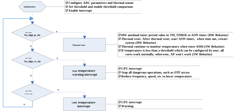
The operation flow is mainly divided into an initialization phase and a continuous monitoring phase. The system continuously compares the sensor output temperature ( ADC CODE ) with three predefined thresholds to adopt different software and hardware protection mechanisms. The specific flow is as follows:
Initialization Phase
After the system starts, it first enters the initialization flow. During this phase, the system executes the following operations sequentially:
Configure the relevant parameters of the Analog-to-Digital Converter (ADC).
Set temperature thresholds and enable the threshold comparison function.
Enable the temperature sensor module.
Enable interrupts to prepare for subsequent temperature warnings and protective actions.
Continuous Monitoring Phase
After initialization is complete, the system enters a continuous temperature threshold determination loop, sequentially performing the following three state detections according to priority:
Over-Temperature Protection Determination (ADC CODE >= tm_high_pt_thr)
The system first determines whether the sensor output temperature ( ADC CODE ) is greater than or equal to the over-temperature protection threshold ( tm_high_pt_thr ).
If the condition is met: Trigger a thermal reset.
Hardware behavior: The hardware automatically loads the timing period value in TM_TIMER into the AON timer. The AON timer is started after the thermal reset is executed, and the system is rebooted after the timer expires.
Software behavior: The system will continue to monitor the temperature after rebooting. If the temperature drops below the user-configured safe threshold, all cores will resume normal operation; otherwise, the Application Processor (AP) will remain in a halted state.
If the condition is not met: Proceed to the next level of determination.
High-Temperature Warning Determination (ADC CODE >= tm_high_wt_thr)
If a thermal reset is not triggered, the system then determines whether the temperature is greater than or equal to the high-temperature warning threshold ( tm_high_wt_thr ).
If the condition is met: Trigger a high-temperature warning interrupt. The system will issue an interrupt request to the CPU, and it is recommended that the user implement strategies such as lowering the main frequency or reducing the operating speed to achieve physical cooling of the system.
If the condition is not met: Proceed to the next level of determination.
Low-Temperature Warning Determination (ADC CODE <= tm_low_wt_thr)
If no high-temperature protection mechanisms are triggered, the system further determines whether the temperature is less than or equal to the low-temperature warning threshold ( tm_low_wt_thr ).
If the condition is met: Trigger a low-temperature warning interrupt, issue an interrupt to the CPU, and report the low-temperature warning.
If the condition is not met: The system performs no action and directly returns to the starting point of the monitoring loop to restart the next round of ADC CODE threshold determination.
The entire process loops repeatedly to ensure reliable operation of the system within the set safe temperature range.
Acquiring Temperature
Temperature values cannot be obtained directly; the following steps are required:
Select thermal (ch8) as the ADC conversion channel.
Start the ADC. The thermal conversion code will be stored in the ADC FIFO or the ch8 data register.
The software reads the data from the ADC FIFO or the ch8 data register and uses the following formula to convert the ADC code into a temperature value.
Temperature = 0.4964 * ADC CODE - 292.3
Interrupt
The thermal sensor supports the following interrupts:
High-temperature warning interrupt (tm_high_wt_thr): Generated when the thermal sensor detects that the temperature reaches or exceeds the high-temperature warning threshold. This interrupt is maskable and is disabled by default.
Low-temperature warning interrupt (tm_low_wt_thr): Generated when the thermal sensor detects that the temperature reaches or drops below the low-temperature warning threshold. This interrupt is maskable and is disabled by default.
Power-on Flow
The power-on flow of the thermal sensor can be described as the following figure.
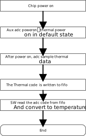
Power-on temperature is the first adc data in ADC FIFO.
Registers
Base Address: 0x4101D000
Name |
Address offset |
Access |
Description |
|---|---|---|---|
000h |
R/W |
Thermal parameter a |
|
004h |
R/W |
Thermal parameter b |
|
008h |
R/W |
Thermal control register,config thermal parameter |
|
00Ch |
R/W |
Thermal threshold control register,config warning and low temperature threshold |
|
010h |
R |
Thermal result register |
|
014h |
R |
Thermal ADC result register,for debug |
|
018h |
R/W |
Record thermal max temperature |
|
01Ch |
R/W |
Record thermal min temperature |
|
020h |
R |
Record thermal output temperature when power on reset |
|
024h |
R/W |
Thermal interrupt control register |
|
028h |
R/W |
Thermal interrupt status register |
|
02Ch |
R/W |
Thermal time register,when over protect temperature,time count value |
|
030h |
R/W |
REG_TM_GAIN
Name: Thermal Meter Gain Register
Size: 32
Address offset: 000h
Read/write access: R/W
Thermal parameter a
Bit |
Symbol |
Access |
INI |
Description |
|---|---|---|---|---|
31:29 |
RSVD |
R |
- |
Reserved |
28:0 |
TM_A |
R/W |
0x08284000 |
This bit defines thermal meter gain.
|
REG_TM_OFFSET
Name: Thermal Meter Offset Register
Size: 32
Address offset: 004h
Read/write access: R/W
Thermal parameter b
Bit |
Symbol |
Access |
INI |
Description |
|---|---|---|---|---|
31:22 |
RSVD |
R |
- |
Reserved |
21:0 |
TM_B |
R/W |
0x00371700 |
This bit defines thermal meter offset.
|
REG_TM_CTRL
Name: Thermal Meter Control Register
Size: 32
Address offset: 008h
Read/write access: R/W
Thermal control register,config thermal parameter
Bit |
Symbol |
Access |
INI |
Description |
|---|---|---|---|---|
31:24 |
TM_PWR |
R/W |
0x69 |
Thm protect password. Tm_pow,tm_powcut,tm_rstb,tm_highcmp_pt_en,tm_high_pt_thr, iso_thm can be programed only when this value is 8’h69. |
23:22 |
RSVD |
R |
- |
Reserved |
21 |
TM_POW |
R/W |
0x1 |
Thermal poweron signal
|
20 |
TM_POWCUT |
R/W |
0x1 |
Power cut
|
19 |
TM_CLK_INV_SEL |
R/W |
0x0 |
Clock phase invert select when read temperature.
|
18 |
TM_RSTB |
R/W |
0x1 |
Thermal reset signal.
|
17:14 |
TM_CHOPFREQSEL |
R/W |
0x1 |
Chop frequecy select
|
13:11 |
TM_OSR |
R/W |
0x0 |
Deci filter DSR select
|
10 |
TM_HOLD_EN |
R/W |
0x0 |
Hold output |
9:8 |
TM_HOLD_DLY |
R/W |
0x1 |
Hold delay, adjust TM_CLK_OUT width |
7 |
TM_CHOP_EN |
R/W |
0x1 |
Chop enable |
6 |
TM_EN_LATCH |
R/W |
0x1 |
Latch thermal sensor output immediately after power on for more accurate test |
5:4 |
TM_BIAS_SEL |
R/W |
0x1 |
Select ADC bias current
|
3 |
TM_BIASDEM_EN |
R/W |
0x1 |
Bias DEM enable |
2:1 |
RSVD |
R |
- |
Reserved |
0 |
TM_ADCCKSEL |
R/W |
0x1 |
Selelct ADC fs
|
REG_TM_TH_CTRL
Name: Thermal Meter Threshold Control Register
Size: 32
Address offset: 00Ch
Read/write access: R/W
Thermal threshold control register,config warning and low temperature threshold
Bit |
Symbol |
Access |
INI |
Description |
|---|---|---|---|---|
31 |
RSVD |
R |
- |
Reserved |
30 |
ISO_THM |
R/W |
0x0 |
|
29 |
TM_HIGHCMP_PT_EN |
R/W |
0x0 |
To enable compare tm_out with over temperature protect threshold: When tm_out[18:10] > tm_high_pt_thr, it will set aon reset.
|
28:20 |
TM_HIGH_PT_THR |
R/W |
0x07D |
Set over temperature protection threshold for comparison with TEMP_OUT. Only between 0x046 (70°C) and 0x08C (140°C) are valid.
|
19 |
TM_HIGHCMP_WT_EN |
R/W |
0x0 |
To enable compare tm_out with over temperature warning threshold: When tm_high_thr <= tm_out[18:10] < tm_high_pt_thr, it will set Interrupt pending flag ISR_TM_HIGH.
|
18:10 |
TM_HIGH_WT_THR |
R/W |
0x069 |
Set the over temperature warning threshold for comparison with TEMP_OUT.Only values greater than 0 are supported
|
9 |
TM_LOWCMP_WT_EN |
R/W |
0x0 |
To enable compare TM_OUT with set Low threshold: When tm_out[18:10] <= tm_low_thr, it will set Interrupt pending flag ISR_TM_LOW.
|
8:0 |
TM_LOW_WT_THR |
R/W |
0x1D8 |
Set the Low threshold for comparison with TEMP_OUT.
|
REG_TM_RESULT
Name: Thermal Meter Temperature Result Register
Size: 32
Address offset: 010h
Read/write access: R
Thermal result register
Bit |
Symbol |
Access |
INI |
Description |
|---|---|---|---|---|
31:19 |
RSVD |
R |
- |
Reserved |
18:0 |
TM_OUT |
R |
0x0 |
This bit defines real temperature. The result refreshes in real time.
|
REG_TM_ADC_RESULT
Name: Thermal Meter ADC Result Register
Size: 32
Address offset: 014h
Read/write access: R
Thermal ADC result register,for debug
Bit |
Symbol |
Access |
INI |
Description |
|---|---|---|---|---|
31:22 |
RSVD |
R |
- |
Reserved |
21:0 |
TM_ADC_OUT |
R |
0x0 |
This bit defines thermal meter ADC output. The result refreshes in real time.
|
REG_TM_MAX_CTRL
Name: Thermal Meter Max Temperature Control Register
Size: 32
Address offset: 018h
Read/write access: R/W
Record thermal max temperature
Bit |
Symbol |
Access |
INI |
Description |
|---|---|---|---|---|
31:20 |
RSVD |
R |
- |
Reserved |
19 |
TM_MAX_CLR |
R/W |
0x0 |
This bit defines clear max temperature
|
18:0 |
TM_MAX |
R |
0x40000 |
These bits define max temperature. |
REG_TM_MIN_CTRL
Name: Thermal Meter Min Temperature Control Register
Size: 32
Address offset: 01Ch
Read/write access: R/W
Record thermal min temperature
Bit |
Symbol |
Access |
INI |
Description |
|---|---|---|---|---|
31:20 |
RSVD |
R |
- |
Reserved |
19 |
TM_MIN_CLR |
R/W |
0x0 |
This bit defines clear min temperature
|
18:0 |
TM_MIN |
R |
0x3FFFF |
These bits define min temperature. |
REG_TM_OUT_PWR_ON
Name: Thermal Meter Power On Temperature Register
Size: 32
Address offset: 020h
Read/write access: R
Record thermal output temperature when power on reset
Bit |
Symbol |
Access |
INI |
Description |
|---|---|---|---|---|
31:19 |
RSVD |
R |
- |
Reserved |
18:0 |
TEMP_OUT_POWERON |
R |
0x0 |
This bit defines output temperature when power on reset.
|
REG_TM_INTR_CTRL
Name: Thermal Meter Interrupt Control Register
Size: 32
Address offset: 024h
Read/write access: R/W
Thermal interrupt control register
Bit |
Symbol |
Access |
INI |
Description |
|---|---|---|---|---|
31:2 |
RSVD |
R |
- |
Reserved |
1 |
IMR_TM_LOW_WT |
R/W |
0x0 |
Interrupt control for thermal meter detect low temperature.
|
0 |
IMR_TM_HIGH_WT |
R/W |
0x0 |
Interrupt control for thermal meter detect over temperature warning.
|
REG_TM_INTR_STS
Name: Thermal Meter Interrupt Status Register
Size: 32
Address offset: 028h
Read/write access: R/W
Thermal interrupt status register
Bit |
Symbol |
Access |
INI |
Description |
|---|---|---|---|---|
31:2 |
RSVD |
R |
- |
Reserved |
1 |
ISR_TM_LOW_WT |
R/W |
0x0 |
Interrupt pending flag for thermal meter detect low temperature.
|
0 |
ISR_TM_HIGH_WT |
R/W |
0x0 |
Interrupt pending flag for thermal meter detect over temperature warning.
|
REG_TM_TIMER
Name: Thermal Meter Timer Register
Size: 32
Address offset: 02Ch
Read/write access: R/W
Thermal time register,when over protect temperature,time count value
Bit |
Symbol |
Access |
INI |
Description |
|---|---|---|---|---|
31:8 |
RSVD |
R |
- |
Reserved |
7:0 |
TIME_PERIOD |
R/W |
0x0F |
Time period of auto power on |
REG_TM_DUMMY
Name: Thermal Dummy Register
Size: 32
Address offset: 030h
Read/write access: R/W
Bit |
Symbol |
Access |
INI |
Description |
|---|---|---|---|---|
31:16 |
RSVD |
R |
- |
Reserved |
15:0 |
DUMMY |
R/W |
0x0 |
Rsvd for hw |
REGISTER_CONTENTS=RTL8720E
REGISTER_CONTENTS=RTL8720E
REGISTER_CONTENTS=RTL8720E
Base Address: 0x42013000
Name |
Address offset |
Access |
Description |
|---|---|---|---|
000h |
R/W |
Thermal parameter a |
|
004h |
R/W |
Thermal parameter b |
|
008h |
R/W |
Thermal control register,config thermal parameter |
|
00Ch |
R/W |
Thermal threshold control register,config warning and low temperature threshold |
|
010h |
R |
Thermal result register |
|
014h |
R |
Thermal ADC result register,for debug |
|
018h |
R/W |
Record thermal max temperature |
|
01Ch |
R/W |
Record thermal min temperature |
|
020h |
R |
Record thermal output temperature when power on reset |
|
024h |
R/W |
Thermal interrupt control register |
|
028h |
R/W |
Thermal interrupt status register |
|
02Ch |
R/W |
Thermal time register,when over protect temperature,time count value |
REG_TM_GAIN
Name: Thermal Meter Gain Register
Size: 32
Address offset: 000h
Read/write access: R/W
Thermal parameter a
Bit |
Symbol |
Access |
INI |
Description |
|---|---|---|---|---|
31:29 |
RSVD |
R |
- |
Reserved |
28:0 |
TM_A |
R/W |
0x08284000 |
This bit defines thermal meter gain.
|
REG_TM_OFFSET
Name: Thermal Meter Offset Register
Size: 32
Address offset: 004h
Read/write access: R/W
Thermal parameter b
Bit |
Symbol |
Access |
INI |
Description |
|---|---|---|---|---|
31:22 |
RSVD |
R |
- |
Reserved |
21:0 |
TM_B |
R/W |
0x00371A00 |
This bit defines thermal meter offset.
|
REG_TM_CTRL
Name: Thermal Meter Control Register
Size: 32
Address offset: 008h
Read/write access: R/W
Thermal control register,config thermal parameter
Bit |
Symbol |
Access |
INI |
Description |
|---|---|---|---|---|
31:24 |
TM_PWR |
R/W |
0x69 |
Thm protect password. Tm_pow,tm_powcut,tm_rstb,tm_highcmp_pt_en can be programed only when this value is 8’h69. |
23:22 |
RSVD |
R |
- |
Reserved |
21 |
TM_POW |
R/W |
0x1 |
Thermal poweron signal
|
20 |
TM_POWCUT |
R/W |
0x1 |
Power cut
|
19 |
TM_CLK_INV_SEL |
R/W |
0x0 |
Clock phase invert select when read temperature.
|
18 |
TM_RSTB |
R/W |
0x1 |
Thermal reset signal.
|
17:14 |
TM_CHOPFREQSEL |
R/W |
0x1 |
Chop frequecy select
|
13:11 |
TM_OSR |
R/W |
0x0 |
Deci filter DSR select
|
10 |
TM_HOLD_EN |
R/W |
0x0 |
Hold output |
9:8 |
TM_HOLD_DLY |
R/W |
0x1 |
Hold delay, adjust TM_CLK_OUT width |
7 |
TM_CHOP_EN |
R/W |
0x1 |
Chop enable |
6 |
TM_EN_LATCH |
R/W |
0x1 |
Latch thermal sensor output immediately after power on for more accurate test |
5:4 |
TM_BIAS_SEL |
R/W |
0x1 |
Select ADC bias current
|
3 |
TM_BIASDEM_EN |
R/W |
0x1 |
Bias DEM enable |
2:1 |
RSVD |
R |
- |
Reserved |
0 |
TM_ADCCKSEL |
R/W |
0x1 |
Selelct ADC fs
|
REG_TM_TH_CTRL
Name: Thermal Meter Threshold Control Register
Size: 32
Address offset: 00Ch
Read/write access: R/W
Thermal threshold control register,config warning and low temperature threshold
Bit |
Symbol |
Access |
INI |
Description |
|---|---|---|---|---|
31:30 |
RSVD |
R |
- |
Reserved |
29 |
TM_HIGHCMP_PT_EN |
R/W |
0x0 |
To enable compare tm_out with over temperature protect threshold: When tm_out[18:10] > tm_high_pt_thr, it will set aon reset.
|
28:20 |
TM_HIGH_PT_THR |
R/W |
0x07D |
Set over temperature protection threshold for comparison with TEMP_OUT. Only between 0x046 (70°C) and 0x08C (140°C) are valid.
|
19 |
TM_HIGHCMP_WT_EN |
R/W |
0x0 |
To enable compare tm_out with over temperature warning threshold: When tm_high_thr <= tm_out[18:10] < tm_high_pt_thr, it will set Interrupt pending flag ISR_TM_HIGH.
|
18:10 |
TM_HIGH_WT_THR |
R/W |
0x069 |
Set the over temperature warning threshold for comparison with TEMP_OUT.Only values greater than 0 are supported
|
9 |
TM_LOWCMP_WT_EN |
R/W |
0x0 |
To enable compare TM_OUT with set Low threshold: When tm_out[18:10] <= tm_low_thr, it will set Interrupt pending flag ISR_TM_LOW.
|
8:0 |
TM_LOW_WT_THR |
R/W |
0x1D8 |
Set the Low threshold for comparison with TEMP_OUT.
|
REG_TM_RESULT
Name: Thermal Meter Temperature Result Register
Size: 32
Address offset: 010h
Read/write access: R
Thermal result register
Bit |
Symbol |
Access |
INI |
Description |
|---|---|---|---|---|
31:19 |
RSVD |
R |
- |
Reserved |
18:0 |
TM_OUT |
R |
0x0 |
This bit defines real temperature. The result refreshes in real time.
|
REG_TM_ADC_RESULT
Name: Thermal Meter ADC Result Register
Size: 32
Address offset: 014h
Read/write access: R
Thermal ADC result register,for debug
Bit |
Symbol |
Access |
INI |
Description |
|---|---|---|---|---|
31:22 |
RSVD |
R |
- |
Reserved |
21:0 |
TM_ADC_OUT |
R |
0x0 |
This bit defines thermal meter ADC output. The result refreshes in real time.
|
REG_TM_MAX_CTRL
Name: Thermal Meter Max Temperature Control Register
Size: 32
Address offset: 018h
Read/write access: R/W
Record thermal max temperature
Bit |
Symbol |
Access |
INI |
Description |
|---|---|---|---|---|
31:20 |
RSVD |
R |
- |
Reserved |
19 |
TM_MAX_CLR |
R/W |
0x0 |
This bit defines clear max temperature
|
18:0 |
TM_MAX |
R |
0x40000 |
These bits define max temperature. |
REG_TM_MIN_CTRL
Name: Thermal Meter Min Temperature Control Register
Size: 32
Address offset: 01Ch
Read/write access: R/W
Record thermal min temperature
Bit |
Symbol |
Access |
INI |
Description |
|---|---|---|---|---|
31:20 |
RSVD |
R |
- |
Reserved |
19 |
TM_MIN_CLR |
R/W |
0x0 |
This bit defines clear min temperature
|
18:0 |
TM_MIN |
R |
0x3FFFF |
These bits define min temperature. |
REG_TM_OUT_PWR_ON
Name: Thermal Meter Power On Temperature Register
Size: 32
Address offset: 020h
Read/write access: R
Record thermal output temperature when power on reset
Bit |
Symbol |
Access |
INI |
Description |
|---|---|---|---|---|
31:19 |
RSVD |
R |
- |
Reserved |
18:0 |
TEMP_OUT_POWERON |
R |
0x0 |
This bit defines output temperature when power on reset.
|
REG_TM_INTR_CTRL
Name: Thermal Meter Interrupt Control Register
Size: 32
Address offset: 024h
Read/write access: R/W
Thermal interrupt control register
Bit |
Symbol |
Access |
INI |
Description |
|---|---|---|---|---|
31:2 |
RSVD |
R |
- |
Reserved |
1 |
IMR_TM_LOW_WT |
R/W |
0x0 |
Interrupt control for thermal meter detect low temperature.
|
0 |
IMR_TM_HIGH_WT |
R/W |
0x0 |
Interrupt control for thermal meter detect over temperature warning.
|
REG_TM_INTR_STS
Name: Thermal Meter Interrupt Status Register
Size: 32
Address offset: 028h
Read/write access: R/W
Thermal interrupt status register
Bit |
Symbol |
Access |
INI |
Description |
|---|---|---|---|---|
31:2 |
RSVD |
R |
- |
Reserved |
1 |
ISR_TM_LOW_WT |
R/W |
0x0 |
Interrupt pending flag for thermal meter detect low temperature.
|
0 |
ISR_TM_HIGH_WT |
R/W |
0x0 |
Interrupt pending flag for thermal meter detect over temperature warning.
|
REG_TM_TIMER
Name: Thermal Meter Timer Register
Size: 32
Address offset: 02Ch
Read/write access: R/W
Thermal time register,when over protect temperature,time count value
Bit |
Symbol |
Access |
INI |
Description |
|---|---|---|---|---|
31:8 |
RSVD |
R |
- |
Reserved |
7:0 |
TIME_PERIOD |
R/W |
0x0F |
Time period of auto power on |
Base Address: 0x40816000
Name |
Address offset |
Access |
Description |
|---|---|---|---|
000h |
R/W |
Thermal parameter a |
|
004h |
R/W |
Thermal parameter b |
|
008h |
R/W |
Thermal control register,config thermal parameter |
|
00Ch |
R/W |
Thermal threshold control register,config warning and low temperature threshold |
|
010h |
R |
Thermal result register |
|
014h |
R |
Thermal ADC result register,for debug |
|
018h |
R/W |
Record thermal max temperature |
|
01Ch |
R/W |
Record thermal min temperature |
|
020h |
R |
Record thermal output temperature when power on reset |
|
024h |
R/W |
Thermal interrupt control register |
|
028h |
R/W |
Thermal interrupt status register |
|
02Ch |
R/W |
Thermal time register,when over protect temperature,time count value |
|
030h |
R/W |
REG_TM_GAIN
Name: Thermal Meter Gain Register
Size: 32
Address offset: 000h
Read/write access: R/W
Thermal parameter a
Bit |
Symbol |
Access |
INI |
Description |
|---|---|---|---|---|
31:29 |
RSVD |
R |
- |
Reserved |
28:0 |
TM_A |
R/W |
0x0834d000 |
This bit defines thermal meter gain.
|
REG_TM_OFFSET
Name: Thermal Meter Offset Register
Size: 32
Address offset: 004h
Read/write access: R/W
Thermal parameter b
Bit |
Symbol |
Access |
INI |
Description |
|---|---|---|---|---|
31:22 |
RSVD |
R |
- |
Reserved |
21:0 |
TM_B |
R/W |
0x00370E00 |
This bit defines thermal meter offset.
|
REG_TM_CTRL
Name: Thermal Meter Control Register
Size: 32
Address offset: 008h
Read/write access: R/W
Thermal control register,config thermal parameter
Bit |
Symbol |
Access |
INI |
Description |
|---|---|---|---|---|
31:24 |
TM_PWR |
R/W |
0x69 |
Thm protect password. Tm_pow,tm_powcut,tm_rstb,tm_highcmp_pt_en,tm_high_pt_thr, iso_thm can be programed only when this value is 8’h69. |
23:22 |
RSVD |
R |
- |
Reserved |
21 |
TM_POW |
R/W |
0x1 |
Thermal poweron signal
|
20 |
TM_POWCUT |
R/W |
0x1 |
Power cut
|
19 |
TM_CLK_INV_SEL |
R/W |
0x0 |
Clock phase invert select when read temperature.
|
18 |
TM_RSTB |
R/W |
0x1 |
Thermal reset signal.
|
17:14 |
TM_CHOPFREQSEL |
R/W |
0x1 |
Chop frequecy select
|
13:11 |
TM_OSR |
R/W |
0x0 |
Deci filter DSR select
|
10 |
TM_HOLD_EN |
R/W |
0x0 |
Hold output |
9:8 |
TM_HOLD_DLY |
R/W |
0x1 |
Hold delay, adjust TM_CLK_OUT width |
7 |
TM_CHOP_EN |
R/W |
0x1 |
Chop enable |
6 |
TM_EN_LATCH |
R/W |
0x1 |
Latch thermal sensor output immediately after power on for more accurate test |
5:4 |
TM_BIAS_SEL |
R/W |
0x1 |
Select ADC bias current
|
3 |
TM_BIASDEM_EN |
R/W |
0x1 |
Bias DEM enable |
2:1 |
RSVD |
R |
- |
Reserved |
0 |
TM_ADCCKSEL |
R/W |
0x1 |
Selelct ADC fs
|
REG_TM_TH_CTRL
Name: Thermal Meter Threshold Control Register
Size: 32
Address offset: 00Ch
Read/write access: R/W
Thermal threshold control register,config warning and low temperature threshold
Bit |
Symbol |
Access |
INI |
Description |
|---|---|---|---|---|
31 |
RSVD |
R |
- |
Reserved |
30 |
ISO_THM |
R/W |
0x0 |
|
29 |
TM_HIGHCMP_PT_EN |
R/W |
0x0 |
To enable compare tm_out with over temperature protect threshold: When tm_out[18:10] > tm_high_pt_thr, it will set aon reset.
|
28:20 |
TM_HIGH_PT_THR |
R/W |
0x07D |
Set over temperature protection threshold for comparison with TEMP_OUT. Only between 0x046 (70°C) and 0x08C (140°C) are valid.
|
19 |
TM_HIGHCMP_WT_EN |
R/W |
0x0 |
To enable compare tm_out with over temperature warning threshold: When tm_high_thr <= tm_out[18:10] < tm_high_pt_thr, it will set Interrupt pending flag ISR_TM_HIGH.
|
18:10 |
TM_HIGH_WT_THR |
R/W |
0x069 |
Set the over temperature warning threshold for comparison with TEMP_OUT.Only values greater than 0 are supported
|
9 |
TM_LOWCMP_WT_EN |
R/W |
0x0 |
To enable compare TM_OUT with set Low threshold: When tm_out[18:10] <= tm_low_thr, it will set Interrupt pending flag ISR_TM_LOW.
|
8:0 |
TM_LOW_WT_THR |
R/W |
0x1D8 |
Set the Low threshold for comparison with TEMP_OUT.
|
REG_TM_RESULT
Name: Thermal Meter Temperature Result Register
Size: 32
Address offset: 010h
Read/write access: R
Thermal result register
Bit |
Symbol |
Access |
INI |
Description |
|---|---|---|---|---|
31:19 |
RSVD |
R |
- |
Reserved |
18:0 |
TM_OUT |
R |
0x0 |
This bit defines real temperature. The result refreshes in real time.
|
REG_TM_ADC_RESULT
Name: Thermal Meter ADC Result Register
Size: 32
Address offset: 014h
Read/write access: R
Thermal ADC result register,for debug
Bit |
Symbol |
Access |
INI |
Description |
|---|---|---|---|---|
31:22 |
RSVD |
R |
- |
Reserved |
21:0 |
TM_ADC_OUT |
R |
0x0 |
This bit defines thermal meter ADC output. The result refreshes in real time.
|
REG_TM_MAX_CTRL
Name: Thermal Meter Max Temperature Control Register
Size: 32
Address offset: 018h
Read/write access: R/W
Record thermal max temperature
Bit |
Symbol |
Access |
INI |
Description |
|---|---|---|---|---|
31:20 |
RSVD |
R |
- |
Reserved |
19 |
TM_MAX_CLR |
R/W |
0x0 |
This bit defines clear max temperature
|
18:0 |
TM_MAX |
R |
0x40000 |
These bits define max temperature. |
REG_TM_MIN_CTRL
Name: Thermal Meter Min Temperature Control Register
Size: 32
Address offset: 01Ch
Read/write access: R/W
Record thermal min temperature
Bit |
Symbol |
Access |
INI |
Description |
|---|---|---|---|---|
31:20 |
RSVD |
R |
- |
Reserved |
19 |
TM_MIN_CLR |
R/W |
0x0 |
This bit defines clear min temperature
|
18:0 |
TM_MIN |
R |
0x3FFFF |
These bits define min temperature. |
REG_TM_OUT_PWR_ON
Name: Thermal Meter Power On Temperature Register
Size: 32
Address offset: 020h
Read/write access: R
Record thermal output temperature when power on reset
Bit |
Symbol |
Access |
INI |
Description |
|---|---|---|---|---|
31:19 |
RSVD |
R |
- |
Reserved |
18:0 |
TEMP_OUT_POWERON |
R |
0x0 |
This bit defines output temperature when power on reset.
|
REG_TM_INTR_CTRL
Name: Thermal Meter Interrupt Control Register
Size: 32
Address offset: 024h
Read/write access: R/W
Thermal interrupt control register
Bit |
Symbol |
Access |
INI |
Description |
|---|---|---|---|---|
31:2 |
RSVD |
R |
- |
Reserved |
1 |
IMR_TM_LOW_WT |
R/W |
0x0 |
Interrupt control for thermal meter detect low temperature.
|
0 |
IMR_TM_HIGH_WT |
R/W |
0x0 |
Interrupt control for thermal meter detect over temperature warning.
|
REG_TM_INTR_STS
Name: Thermal Meter Interrupt Status Register
Size: 32
Address offset: 028h
Read/write access: R/W
Thermal interrupt status register
Bit |
Symbol |
Access |
INI |
Description |
|---|---|---|---|---|
31:2 |
RSVD |
R |
- |
Reserved |
1 |
ISR_TM_LOW_WT |
R/W |
0x0 |
Interrupt pending flag for thermal meter detect low temperature.
|
0 |
ISR_TM_HIGH_WT |
R/W |
0x0 |
Interrupt pending flag for thermal meter detect over temperature warning.
|
REG_TM_TIMER
Name: Thermal Meter Timer Register
Size: 32
Address offset: 02Ch
Read/write access: R/W
Thermal time register,when over protect temperature,time count value
Bit |
Symbol |
Access |
INI |
Description |
|---|---|---|---|---|
31:8 |
RSVD |
R |
- |
Reserved |
7:0 |
TIME_PERIOD |
R/W |
0x0F |
Time period of auto power on |
REG_TM_DUMMY
Name: Thermal Dummy Register
Size: 32
Address offset: 030h
Read/write access: R/W
Bit |
Symbol |
Access |
INI |
Description |
|---|---|---|---|---|
31:16 |
RSVD |
R |
- |
Reserved |
15:0 |
DUMMY |
R/W |
0x0 |
Rsvd for hw |
ADC Registers
Base Address: 0x40803000
Name |
Address offset |
Access |
Description |
|---|---|---|---|
000h |
R/W |
Basic configuration of ADC including enable and operation mode |
|
008h |
R/W |
Channel comparison threshold |
|
00Ch |
R/W |
Refer to REG_ADC_COMP_TH_CH0 |
|
010h |
R/W |
Refer to REG_ADC_COMP_TH_CH0 |
|
014h |
R/W |
Refer to REG_ADC_COMP_TH_CH0 |
|
018h |
R/W |
Refer to REG_ADC_COMP_TH_CH0 |
|
01Ch |
R/W |
Refer to REG_ADC_COMP_TH_CH0 |
|
020h |
R/W |
Refer to REG_ADC_COMP_TH_CH0 |
|
024h |
R/W |
Refer to REG_ADC_COMP_TH_CH0 |
|
034h |
R/W |
Channel comparison criterion control register, can be used to control every channel’s comparison criterion. There are 3 kinds of criterions. |
|
038h |
R |
The comparison status of every channel |
|
03Ch |
R/W |
Software channel list 0, to define the analog channels to own channel list |
|
040h |
R/W |
Software channel list 1, refer to REG_ADC_CHSW_LIST_0 |
|
048h |
R/W |
Automatic switch channel function |
|
04Ch |
R/W |
Software controls to trigger the channel switch |
|
050h |
R |
The register records the last channel |
|
054h |
R |
The register reflects the ADC FSM and fifo status |
|
058h |
R/W |
The register to enable or disable the different kinds of interrupts |
|
05Ch |
R |
The register to record the different kinds of interrupt raw status(bypass the enable register’s control) |
|
060h |
R/W |
The register to record the different kinds of interrupt status |
|
064h |
R/W |
The specific channel to trigger interrupt |
|
068h |
R/W |
The fifo full threshold |
|
06Ch |
R/W |
The register to select the specific external timer source |
|
070h |
R |
The register to store the channel data , ready and overwritten information |
|
074h |
R |
Refer to REG_ADC_DATA_CH0 |
|
078h |
R |
Refer to REG_ADC_DATA_CH0 |
|
07Ch |
R |
Refer to REG_ADC_DATA_CH0 |
|
080h |
R |
Refer to REG_ADC_DATA_CH0 |
|
084h |
R |
Refer to REG_ADC_DATA_CH0 |
|
088h |
R |
Refer to REG_ADC_DATA_CH0 |
|
08Ch |
R |
Refer to REG_ADC_DATA_CH0 |
|
090h |
R |
Refer to REG_ADC_DATA_CH0 |
|
09Ch |
R |
Register to store global data, ready , channel and overwritten information |
|
0A0h |
R |
Register to store fifo entry number |
|
0A4h |
R/W |
Register to clear fifo |
|
0A8h |
R/W |
Register to control clock dividend and channel unmask |
|
0ACh |
R/W |
Register to configure ADC over sample |
|
0B0h |
R/W |
Register to control the ADC power and debug configuration |
|
0B4h |
R/W |
Register to set the software test mode |
|
0B8h |
R/W |
||
0BCh |
R/W |
||
0C0h |
R/W |
||
0C4h |
R/W |
||
0C8h |
R/W |
||
0CCh |
R/W |
||
0D0h |
R/W |
||
0D4h |
R/W |
Dummy register |
REG_ADC_CONF
Name: ADC Configuration Register
Size: 32
Address offset: 000h
Read/write access: R/W
Basic configuration of ADC including enable and operation mode
Bit |
Symbol |
Access |
INI |
Description |
|---|---|---|---|---|
31:10 |
RSVD |
R |
- |
Reserved |
9 |
BIT_ADC_ENABLE |
R/W |
1h |
This bit is for ADC enable control |
8 |
RSVD |
R |
- |
Reserved |
7:4 |
BIT_ADC_CVLIST_LEN |
R/W |
0h |
This field defines the number of items in the ADC conversion channel list. |
3:1 |
BIT_ADC_OP_MOD |
R/W |
1h |
These bits selects ADC operation mode. 0: software trigger mode.
|
0 |
RSVD |
R |
- |
Reserved |
REG_ADC_COMP_TH_CH0
Name: ADC Channel 0 Comparison Threshold Register
Size: 32
Address offset: 008h
Read/write access: R/W
Channel comparison threshold
Bit |
Symbol |
Access |
INI |
Description |
|---|---|---|---|---|
31:16 |
BIT_ADC_COMP_TH_H_CH0 |
R/W |
0h |
This field defines the higher threshold of channel 0 for ADC automatic comparison. |
15:0 |
BIT_ADC_COMP_TH_L_CH0 |
R/W |
0h |
This field defines the lower threshold of channel 0 for ADC automatic comparison. |
REG_ADC_COMP_TH_CH1
Name: ADC Channel 1 Comparison Threshold Register
Size: 32
Address offset: 00Ch
Read/write access: R/W
Refer to REG_ADC_COMP_TH_CH0
Bit |
Symbol |
Access |
INI |
Description |
|---|---|---|---|---|
31:16 |
BIT_ADC_COMP_TH_H_CH1 |
R/W |
0h |
This field defines the higher threshold of channel 1 for ADC automatic comparison. |
15:0 |
BIT_ADC_COMP_TH_L_CH1 |
R/W |
0h |
This field defines the lower threshold of channel 1 for ADC automatic comparison. |
REG_ADC_COMP_TH_CH2
Name: ADC Channel 2 Comparison Threshold Register
Size: 32
Address offset: 010h
Read/write access: R/W
Refer to REG_ADC_COMP_TH_CH0
Bit |
Symbol |
Access |
INI |
Description |
|---|---|---|---|---|
31:16 |
BIT_ADC_COMP_TH_H_CH2 |
R/W |
0h |
This field defines the higher threshold of channel 2 for ADC automatic comparison. |
15:0 |
BIT_ADC_COMP_TH_L_CH2 |
R/W |
0h |
This field defines the lower threshold of channel 2 for ADC automatic comparison. |
REG_ADC_COMP_TH_CH3
Name: ADC Channel 3 Comparison Threshold Register
Size: 32
Address offset: 014h
Read/write access: R/W
Refer to REG_ADC_COMP_TH_CH0
Bit |
Symbol |
Access |
INI |
Description |
|---|---|---|---|---|
31:16 |
BIT_ADC_COMP_TH_H_CH3 |
R/W |
0h |
This field defines the higher threshold of channel 3 for ADC automatic comparison. |
15:0 |
BIT_ADC_COMP_TH_L_CH3 |
R/W |
0h |
This field defines the lower threshold of channel 3 for ADC automatic comparison. |
REG_ADC_COMP_TH_CH4
Name: ADC Channel 4 Comparison Threshold Register
Size: 32
Address offset: 018h
Read/write access: R/W
Refer to REG_ADC_COMP_TH_CH0
Bit |
Symbol |
Access |
INI |
Description |
|---|---|---|---|---|
31:16 |
BIT_ADC_COMP_TH_H_CH4 |
R/W |
0h |
This field defines the higher threshold of channel 4 for ADC automatic comparison. |
15:0 |
BIT_ADC_COMP_TH_L_CH4 |
R/W |
0h |
This field defines the lower threshold of channel 4 for ADC automatic comparison. |
REG_ADC_COMP_TH_CH5
Name: ADC Channel 5 Comparison Threshold Register
Size: 32
Address offset: 01Ch
Read/write access: R/W
Refer to REG_ADC_COMP_TH_CH0
Bit |
Symbol |
Access |
INI |
Description |
|---|---|---|---|---|
31:16 |
BIT_ADC_COMP_TH_H_CH5 |
R/W |
0h |
This field defines the higher threshold of channel 5 for ADC automatic comparison. |
15:0 |
BIT_ADC_COMP_TH_L_CH5 |
R/W |
0h |
This field defines the lower threshold of channel 5 for ADC automatic comparison. |
REG_ADC_COMP_TH_CH6
Name: ADC Channel 6 Comparison Threshold Register
Size: 32
Address offset: 020h
Read/write access: R/W
Refer to REG_ADC_COMP_TH_CH0
Bit |
Symbol |
Access |
INI |
Description |
|---|---|---|---|---|
31:16 |
BIT_ADC_COMP_TH_H_CH6 |
R/W |
0h |
This field defines the higher threshold of channel 6 for ADC automatic comparison. |
15:0 |
BIT_ADC_COMP_TH_L_CH6 |
R/W |
0h |
This field defines the lower threshold of channel 6 for ADC automatic comparison. |
REG_ADC_COMP_TH_CH7
Name: ADC Channel 7 Comparison Threshold Register
Size: 32
Address offset: 024h
Read/write access: R/W
Refer to REG_ADC_COMP_TH_CH0
Bit |
Symbol |
Access |
INI |
Description |
|---|---|---|---|---|
31:16 |
BIT_ADC_COMP_TH_H_CH7 |
R/W |
0h |
This field defines the higher threshold of channel 7 for ADC automatic comparison. |
15:0 |
BIT_ADC_COMP_TH_L_CH7 |
R/W |
0h |
This field defines the lower threshold of channel 7 for ADC automatic comparison. |
REG_ADC_COMP_CTRL
Name: ADC Comparison Control Register
Size: 32
Address offset: 034h
Read/write access: R/W
Channel comparison criterion control register, can be used to control every channel’s comparison
criterion. There are 3 kinds of criterions.
Bit |
Symbol |
Access |
INI |
Description |
|---|---|---|---|---|
31:16 |
RSVD |
R |
- |
Reserved |
15:14 |
BIT_ADC_COMP_CTRL_CH7 |
R/W |
0h |
The function is same as bit_adc_comp_ctrl_ch10 |
13:12 |
BIT_ADC_COMP_CTRL_CH6 |
R/W |
0h |
The function is same as bit_adc_comp_ctrl_ch10 |
11:10 |
BIT_ADC_COMP_CTRL_CH5 |
R/W |
0h |
The function is same as bit_adc_comp_ctrl_ch10 |
9:8 |
BIT_ADC_COMP_CTRL_CH4 |
R/W |
0h |
The function is same as bit_adc_comp_ctrl_ch10 |
7:6 |
BIT_ADC_COMP_CTRL_CH3 |
R/W |
0h |
The function is same as bit_adc_comp_ctrl_ch10 |
5:4 |
BIT_ADC_COMP_CTRL_CH2 |
R/W |
0h |
The function is same as bit_adc_comp_ctrl_ch10 |
3:2 |
BIT_ADC_COMP_CTRL_CH1 |
R/W |
0h |
The function is same as bit_adc_comp_ctrl_ch10 |
1:0 |
BIT_ADC_COMP_CTRL_CH0 |
R/W |
0h |
The function is same as bit_adc_comp_ctrl_ch10 |
REG_ADC_COMP_STS
Name: ADC Comparison Status Register
Size: 32
Address offset: 038h
Read/write access: R
The comparison status of every channel
Bit |
Symbol |
Access |
INI |
Description |
|---|---|---|---|---|
31:16 |
RSVD |
R |
- |
Reserved |
15:14 |
BIT_ADC_COMP_STS_CH7 |
R |
0h |
This field reflects the comparison result of channel 7 immediately |
13:12 |
BIT_ADC_COMP_STS_CH6 |
R |
0h |
This field reflects the comparison result of channel 6 immediately |
11:10 |
BIT_ADC_COMP_STS_CH5 |
R |
0h |
This field reflects the comparison result of channel 5 immediately |
9:8 |
BIT_ADC_COMP_STS_CH4 |
R |
0h |
This field reflects the comparison result of channel 4 immediately |
7:6 |
BIT_ADC_COMP_STS_CH3 |
R |
0h |
This field reflects the comparison result of channel 3 immediately |
5:4 |
BIT_ADC_COMP_STS_CH2 |
R |
0h |
This field reflects the comparison result of channel 2 immediately |
3:2 |
BIT_ADC_COMP_STS_CH1 |
R |
0h |
This field reflects the comparison result of channel 1 immediately |
1:0 |
BIT_ADC_COMP_STS_CH0 |
R |
0h |
This field reflects the comparison result of channel 0 immediately |
REG_ADC_CHSW_LIST_0
Name: ADC Channel Switch List 0 Register
Size: 32
Address offset: 03Ch
Read/write access: R/W
Software channel list 0, to define the analog channels to own channel list
Bit |
Symbol |
Access |
INI |
Description |
|---|---|---|---|---|
31:28 |
BIT_ADC_CHSW_7 |
R/W |
0h |
This field defines the number 7 channel to do a conversion when a conversion event takes place. |
27:24 |
BIT_ADC_CHSW_6 |
R/W |
0h |
This field defines the number 6 channel to do a conversion when a conversion event takes place. |
23:20 |
BIT_ADC_CHSW_5 |
R/W |
0h |
This field defines the number 5 channel to do a conversion when a conversion event takes place. |
19:16 |
BIT_ADC_CHSW_4 |
R/W |
0h |
This field defines the number 4 channel to do a conversion when a conversion event takes place. |
15:12 |
BIT_ADC_CHSW_3 |
R/W |
0h |
This field defines the number 3 channel to do a conversion when a conversion event takes place. |
11:8 |
BIT_ADC_CHSW_2 |
R/W |
0h |
This field defines the number 2 channel to do a conversion when a conversion event takes place. |
7:4 |
BIT_ADC_CHSW_1 |
R/W |
0h |
This field defines the number 1 channel to do a conversion when a conversion event takes place. |
3:0 |
BIT_ADC_CHSW_0 |
R/W |
4’h8 |
This field defines the number 0 channel to do a conversion when a conversion event takes place. |
REG_ADC_CHSW_LIST_1
Name: ADC Channel Switch List 1 Register
Size: 32
Address offset: 040h
Read/write access: R/W
Software channel list 1, refer to REG_ADC_CHSW_LIST_0
Bit |
Symbol |
Access |
INI |
Description |
|---|---|---|---|---|
31:28 |
BIT_ADC_CHSW_15 |
R/W |
0h |
This field defines the number 15 channel to do a conversion when a conversion event takes place. |
27:24 |
BIT_ADC_CHSW_14 |
R/W |
0h |
This field defines the number 14 channel to do a conversion when a conversion event takes place. |
23:20 |
BIT_ADC_CHSW_13 |
R/W |
0h |
This field defines the number 13 channel to do a conversion when a conversion event takes place. |
19:16 |
BIT_ADC_CHSW_12 |
R/W |
0h |
This field defines the number 12 channel to do a conversion when a conversion event takes place. |
15:12 |
BIT_ADC_CHSW_11 |
R/W |
0h |
This field defines the number 11 channel to do a conversion when a conversion event takes place. |
11:8 |
BIT_ADC_CHSW_10 |
R/W |
0h |
This field defines the number 10 channel to do a conversion when a conversion event takes place. |
7:4 |
BIT_ADC_CHSW_9 |
R/W |
0h |
This field defines the number 9 channel to do a conversion when a conversion event takes place. |
3:0 |
BIT_ADC_CHSW_8 |
R/W |
0h |
This field defines the number 8 channel to do a conversion when a conversion event takes place. |
REG_ADC_AUTO_CSW_CTRL
Name: ADC Automatic Channel Switch Control Register
Size: 32
Address offset: 048h
Read/write access: R/W
Automatic switch channel function
Bit |
Symbol |
Access |
INI |
Description |
|---|---|---|---|---|
31:1 |
RSVD |
R |
- |
Reserved |
0 |
BIT_ADC_AUTOSW_EN |
R/W |
0h |
This bit controls the automatic channel switch enabled or disabled.
|
REG_ADC_SW_TRIG
Name: ADC Software Trigger Register
Size: 32
Address offset: 04Ch
Read/write access: R/W
Software controls to trigger the channel switch
Bit |
Symbol |
Access |
INI |
Description |
|---|---|---|---|---|
31:1 |
RSVD |
R |
- |
Reserved |
0 |
BIT_ADC_SW_TRIG |
R/W |
0h |
This bit controls the ADC module to do a conversion. Every time this bit is set to 1, ADC module would switch to a new channel and do one conversion. Therefore, this bit could be used as a start-convert event which is controlled by software. Every time a conversion is done, software MUST clear this bit manually. The interval between clearing and restart this bit must exceed one sample clock period.
|
REG_ADC_LAST_CH
Name: ADC Last Channel Register
Size: 32
Address offset: 050h
Read/write access: R
The register records the last channel
Bit |
Symbol |
Access |
INI |
Description |
|---|---|---|---|---|
31:4 |
RSVD |
R |
- |
Reserved |
3:0 |
BIT_ADC_LAST_CH |
R |
0h |
This field reflects the last used channel |
REG_ADC_BUSY_STS
Name: ADC Busy Status Register
Size: 32
Address offset: 054h
Read/write access: R
The register reflects the ADC FSM and fifo status
Bit |
Symbol |
Access |
INI |
Description |
|---|---|---|---|---|
31:3 |
RSVD |
R |
- |
Reserved |
2 |
BIT_ADC_FIFO_EMPTY |
R |
1 |
|
1 |
BIT_ADC_FIFO_FULL_REAL |
R |
0 |
|
0 |
BIT_ADC_BUSY_STS |
R |
0 |
This bit reflects the ADC is busy or not. If the ADC is processing a conversion of a channel, this bit remains 1 which indicates it’s busy. Once a conversion is done, this bit becomes 0 which indicates it’s ready to do another conversion.
|
REG_ADC_INTR_CTRL
Name: ADC Interrupt Control Register
Size: 32
Address offset: 058h
Read/write access: R/W
The register to enable or disable the different kinds of interrupts
Bit |
Symbol |
Access |
INI |
Description |
|---|---|---|---|---|
31 |
BIT_ADC_IT_COMP_DET_MOD |
R/W |
0h |
This bit controls the interrupt bit_adc_it_comp_chx operation. comparison criterion matching is rising edge.
|
30:22 |
RSVD |
R |
- |
Reserved |
21 |
BIT_ADC_IT_TM_LOW_WT_EN |
R/W |
0h |
Interrupt control for thermal meter detect low temperature.
|
20 |
BIT_ADC_IT_TM_HIGH_WT_EN |
R/W |
0h |
Interrupt control for thermal meter detect over temperature warning.
|
19 |
BIT_ADC_BREAK_TIMEOUT_EN |
R/W |
0h |
When the ADC does not respond for a long time due to CTC occupation, an interrupt will be triggered.
|
18:16 |
RSVD |
R |
- |
Reserved |
15 |
BIT_ADC_IT_COMP_CH7_EN |
R/W |
0h |
The function is same as bit_adc_it_comp_ch0_en |
14 |
BIT_ADC_IT_COMP_CH6_EN |
R/W |
0h |
The function is same as bit_adc_it_comp_ch0_en |
13 |
BIT_ADC_IT_COMP_CH5_EN |
R/W |
0h |
The function is same as bit_adc_it_comp_ch0_en |
12 |
BIT_ADC_IT_COMP_CH4_EN |
R/W |
0h |
The function is same as bit_adc_it_comp_ch0_en |
11 |
BIT_ADC_IT_COMP_CH3_EN |
R/W |
0h |
The function is same as bit_adc_it_comp_ch0_en |
10 |
BIT_ADC_IT_COMP_CH2_EN |
R/W |
0h |
The function is same as bit_adc_it_comp_ch0_en |
9 |
BIT_ADC_IT_COMP_CH1_EN |
R/W |
0h |
The function is same as bit_adc_it_comp_ch0_en |
8 |
BIT_ADC_IT_COMP_CH0_EN |
R/W |
0h |
This bit controls the interrupt is enabled or not when channel 0 comparison criterion matches.
|
7 |
BIT_ADC_IT_ERR_EN |
R/W |
0h |
This bit controls the interrupt is enabled or not when an error state takes place.
|
6 |
BIT_ADC_IT_DAT_OVW_EN |
R/W |
0h |
This bit controls the interrupt is enabled or not when a data overwritten situation takes place.
|
5 |
BIT_ADC_IT_FIFO_EMPTY_EN |
R/W |
0h |
This bit controls the interrupt is enabled or not when a FIFO empty state takes place.
|
4 |
BIT_ADC_IT_FIFO_OVER_EN |
R/W |
0h |
This bit controls the interrupt is enabled or not when a FIFO overflow state takes place.
|
3 |
BIT_ADC_IT_FIFO_FULL_EN |
R/W |
0h |
This bit controls the interrupt is enabled or not when a FIFO full state takes place.
|
2 |
BIT_ADC_IT_CHCV_END_EN |
R/W |
0h |
This bit controls the interrupt is enabled or not when a particular channel conversion is done. Please refer to reg_adc_it_chno_con
|
1 |
BIT_ADC_IT_CV_END_EN |
R/W |
0h |
This bit controls the interrupt is enabled or not every time a conversion is done. No matter ADC module is in what kind of operation mode. Every time a conversion is executed, ADC module would notify system if This bit is set.
|
0 |
BIT_ADC_IT_CVLIST_END_EN |
R/W |
0h |
This bit controls the interrupt is enabled or not when a conversion of the last channel in the list is done. For example, in automatic mode conversions would be executed continuously. Every time the last channel conversion is done, which means all channel conversions in the list is done, ADC could notify system if This bit is set.
|
REG_ADC_INTR_RAW_STS
Name: ADC Interrupt Raw Status Register
Size: 32
Address offset: 05Ch
Read/write access: R
The register to record the different kinds of interrupt raw status(bypass the enable register’s
control)
Bit |
Symbol |
Access |
INI |
Description |
|---|---|---|---|---|
31:22 |
RSVD |
R |
- |
Reserved |
21 |
BIT_ADC_IT_TM_LOW_WT_RAW_STS |
R |
0h |
|
20 |
BIT_ADC_IT_TM_HIGH_WT_RAW_STS |
R |
0h |
Merged |
19 |
BIT_ADC_BREAK_TIMEOUT_RAW_STS |
R |
0h |
Merged |
18:16 |
RSVD |
R |
- |
Reserved |
15 |
BIT_ADC_IT_COMP_CH7_RAW_STS |
R |
0h |
Merged |
14 |
BIT_ADC_IT_COMP_CH6_RAW_STS |
R |
0h |
Merged |
13 |
BIT_ADC_IT_COMP_CH5_RAW_STS |
R |
0h |
Merged |
12 |
BIT_ADC_IT_COMP_CH4_RAW_STS |
R |
0h |
Merged |
11 |
BIT_ADC_IT_COMP_CH3_RAW_STS |
R |
0h |
Merged |
10 |
BIT_ADC_IT_COMP_CH2_RAW_STS |
R |
0h |
Merged |
9 |
BIT_ADC_IT_COMP_CH1_RAW_STS |
R |
0h |
Merged |
8 |
BIT_ADC_IT_COMP_CH0_RAW_STS |
R |
0h |
Merged |
7 |
BIT_ADC_IT_ERR_RAW_STS |
R |
0h |
Merged |
6 |
BIT_ADC_IT_DAT_OVW_RAW_STS |
R |
0h |
Merged |
5 |
BIT_ADC_IT_FIFO_EMPTY_RAW_STS |
R |
1h |
Merged |
4 |
BIT_ADC_IT_FIFO_OVER_RAW_STS |
R |
0h |
Merged |
3 |
BIT_ADC_IT_FIFO_FULL_RAW_STS |
R |
0h |
Merged |
2 |
BIT_ADC_IT_CHCV_END_RAW_STS |
R |
0h |
Merged |
1 |
BIT_ADC_IT_CV_END_RAW_STS |
R |
0h |
Merged |
0 |
BIT_ADC_IT_CVLIST_END_RAW_STS |
R |
0h |
Merged |
REG_ADC_INTR_STS
Name: ADC Interrupt Status Register
Size: 32
Address offset: 060h
Read/write access: R/W
The register to record the different kinds of interrupt status
Bit |
Symbol |
Access |
INI |
Description |
|---|---|---|---|---|
31:22 |
RSVD |
R |
- |
Reserved |
21 |
BIT_ADC_IT_TM_LOW_WT_STS |
R/W |
0h |
|
20 |
BIT_ADC_IT_TM_HIGH_WT_STS |
R/W |
0h |
|
19 |
BIT_ADC_BREAK_TIMEOUT_STS |
R/W |
0h |
|
18:16 |
RSVD |
R |
- |
Reserved |
15 |
BIT_ADC_IT_COMP_CH7_STS |
R/W |
0h |
Merged |
14 |
BIT_ADC_IT_COMP_CH6_STS |
R/W |
0h |
Merged |
13 |
BIT_ADC_IT_COMP_CH5_STS |
R/W |
0h |
Merged |
12 |
BIT_ADC_IT_COMP_CH4_STS |
R/W |
0h |
Merged |
11 |
BIT_ADC_IT_COMP_CH3_STS |
R/W |
0h |
Merged |
10 |
BIT_ADC_IT_COMP_CH2_STS |
R/W |
0h |
Merged |
9 |
BIT_ADC_IT_COMP_CH1_STS |
R/W |
0h |
Merged |
8 |
BIT_ADC_IT_COMP_CH0_STS |
R/W |
0h |
Merged |
7 |
BIT_ADC_IT_ERR_STS |
R/W |
0h |
Merged |
6 |
BIT_ADC_IT_DAT_OVW_STS |
R/W |
0h |
Merged |
5 |
BIT_ADC_IT_FIFO_EMPTY_STS |
R/W |
0h |
Merged |
4 |
BIT_ADC_IT_FIFO_OVER_STS |
R/W |
0h |
Merged |
3 |
BIT_ADC_IT_FIFO_FULL_STS |
R/W |
0h |
Merged |
2 |
BIT_ADC_IT_CHCV_END_STS |
R/W |
0h |
Merged |
1 |
BIT_ADC_IT_CV_END_STS |
R/W |
0h |
Merged |
0 |
BIT_ADC_IT_CVLIST_END_STS |
R/W |
0h |
Merged |
REG_ADC_IT_CHNO_CON
Name: ADC Interrupt Channel Number Configuration Register
Size: 32
Address offset: 064h
Read/write access: R/W
The specific channel to trigger interrupt
Bit |
Symbol |
Access |
INI |
Description |
|---|---|---|---|---|
31:4 |
RSVD |
R |
- |
Reserved |
3:0 |
BIT_ADC_IT_CHNO_CON |
R/W |
0h |
This field defines that ADC module should send interrupt signal to system when a conversion which of channel number is the same as this field. This register is only valid when bit_adc_it_chcv_end_en is set. Bit_adc_it_chno_con: channel number |
REG_ADC_FULL_LVL
Name: ADC FIFO Full Threshold Register
Size: 32
Address offset: 068h
Read/write access: R/W
The fifo full threshold
Bit |
Symbol |
Access |
INI |
Description |
|---|---|---|---|---|
31:6 |
RSVD |
R |
- |
Reserved |
5:0 |
BIT_ADC_FULL_LVL |
R/W |
0h |
This field defines the FIFO full entry thredshold level and it’s used for FIFO full interrupt. It should be set according to ADC FIFO depth. A value of 0 sets the threshold for 1 entry, and a value of 15 sets the threshold for 16 entries. |
REG_ADC_EXT_TRIG_TIMER_SEL
Name: ADC External Trigger Timer Select Register
Size: 32
Address offset: 06Ch
Read/write access: R/W
The register to select the specific external timer source
Bit |
Symbol |
Access |
INI |
Description |
|---|---|---|---|---|
31:3 |
RSVD |
R |
- |
Reserved |
2:0 |
BIT_ADC_EXT_TRIG_TIMER_SEL |
R/W |
0h |
These three bits defines which timer channel would be used to make ADC module do a conversion.
|
REG_ADC_DATA_CH0
Name: ADC Channel 0 Data Register
Size: 32
Address offset: 070h
Read/write access: R
The register to store the channel data , ready and overwritten information
Bit |
Symbol |
Access |
INI |
Description |
|---|---|---|---|---|
31:22 |
RSVD |
R |
- |
Reserved |
21 |
BIT_ADC_DAT_RDY_CH0 |
R |
0 |
This bit indicates that a conversion is done. Every time a conversion is done, this bit should be set to 1 and it would be cleared to 0 when a read operation of reg_adc_data_ch0. |
20 |
BIT_ADC_DAT_OVW_CH0 |
R |
0 |
This bit indicates that there is a data overwritten situation in bit_adc_data_global takeing place. A data overwritten situation is that a former conversion data is NOT read before a new conversion is written to data field. It would be cleared to 0 when a read operation of reg_adc_data_ch0.
|
19:16 |
BIT_ADC_NUM_CH0 |
R |
0 |
This field contains the newsest conversion data of channel 0 [19:16]: which channel in channel list the data belongs to, only valid when bit_adc_ch_unmask=1 |
15:0 |
BIT_ADC_DATA_CH0 |
R |
0 |
This field contains the newsest conversion data of channel 0 [15:0]: newest data |
REG_ADC_DATA_CH1
Name: ADC Channel 1 Data Register
Size: 32
Address offset: 074h
Read/write access: R
Refer to REG_ADC_DATA_CH0
Bit |
Symbol |
Access |
INI |
Description |
|---|---|---|---|---|
31:22 |
RSVD |
R |
- |
Reserved |
21 |
BIT_ADC_DAT_RDY_CH1 |
R |
0 |
This bit indicates that a conversion is done. Every time a conversion is done, this bit should be set to 1 and it would be cleared to 0 when a read operation of reg_adc_data_ch1. |
20 |
BIT_ADC_DAT_OVW_CH1 |
R |
0 |
This bit indicates that there is a data overwritten situation in bit_adc_data_global takeing place. A data overwritten situation is that a former conversion data is NOT read before a new conversion is written to data field. It would be cleared to 0 when a read operation of reg_adc_data_ch1.
|
19:16 |
BIT_ADC_NUM_CH1 |
R |
0 |
This field contains the newsest conversion data of channel 1 [19:16]: which channel in channel list the data belongs to, only valid when bit_adc_ch_unmask=1 |
15:0 |
BIT_ADC_DATA_CH1 |
R |
0 |
This field contains the newsest conversion data of channel 1 [15:0]: newest data |
REG_ADC_DATA_CH2
Name: ADC Channel 2 Data Register
Size: 32
Address offset: 078h
Read/write access: R
Refer to REG_ADC_DATA_CH0
Bit |
Symbol |
Access |
INI |
Description |
|---|---|---|---|---|
31:22 |
RSVD |
R |
- |
Reserved |
21 |
BIT_ADC_DAT_RDY_CH2 |
R |
0 |
This bit indicates that a conversion is done. Every time a conversion is done, this bit should be set to 1 and it would be cleared to 0 when a read operation of reg_adc_data_ch2. |
20 |
BIT_ADC_DAT_OVW_CH2 |
R |
0 |
This bit indicates that there is a data overwritten situation in bit_adc_data_global takeing place. A data overwritten situation is that a former conversion data is NOT read before a new conversion is written to data field. It would be cleared to 0 when a read operation of reg_adc_data_ch2.
|
19:16 |
BIT_ADC_NUM_CH2 |
R |
0 |
This field contains the newsest conversion data of channel 2 [19:16]: which channel in channel list the data belongs to, only valid when bit_adc_ch_unmask=1 |
15:0 |
BIT_ADC_DATA_CH2 |
R |
0 |
This field contains the newsest conversion data of channel 2 [15:0]: newest data |
REG_ADC_DATA_CH3
Name: ADC Channel 3 Data Register
Size: 32
Address offset: 07Ch
Read/write access: R
Refer to REG_ADC_DATA_CH0
Bit |
Symbol |
Access |
INI |
Description |
|---|---|---|---|---|
31:22 |
RSVD |
R |
- |
Reserved |
21 |
BIT_ADC_DAT_RDY_CH3 |
R |
0 |
This bit indicates that a conversion is done. Every time a conversion is done, this bit should be set to 1 and it would be cleared to 0 when a read operation of reg_adc_data_ch3. |
20 |
BIT_ADC_DAT_OVW_CH3 |
R |
0 |
This bit indicates that there is a data overwritten situation in bit_adc_data_global takeing place. A data overwritten situation is that a former conversion data is NOT read before a new conversion is written to data field. It would be cleared to 0 when a read operation of reg_adc_data_ch3.
|
19:16 |
BIT_ADC_NUM_CH3 |
R |
0 |
This field contains the newsest conversion data of channel 3 [19:16]: which channel in channel list the data belongs to, only valid when bit_adc_ch_unmask=1 |
15:0 |
BIT_ADC_DATA_CH3 |
R |
0 |
This field contains the newsest conversion data of channel 3 [15:0]: newest data |
REG_ADC_DATA_CH4
Name: ADC Channel 4 Data Register
Size: 32
Address offset: 080h
Read/write access: R
Refer to REG_ADC_DATA_CH0
Bit |
Symbol |
Access |
INI |
Description |
|---|---|---|---|---|
31:22 |
RSVD |
R |
- |
Reserved |
21 |
BIT_ADC_DAT_RDY_CH4 |
R |
0 |
This bit indicates that a conversion is done. Every time a conversion is done, this bit should be set to 1 and it would be cleared to 0 when a read operation of reg_adc_data_ch4. |
20 |
BIT_ADC_DAT_OVW_CH4 |
R |
0 |
This bit indicates that there is a data overwritten situation in bit_adc_data_global takeing place. A data overwritten situation is that a former conversion data is NOT read before a new conversion is written to data field. It would be cleared to 0 when a read operation of reg_adc_data_ch4.
|
19:16 |
BIT_ADC_NUM_CH4 |
R |
0 |
This field contains the newsest conversion data of channel 4 [19:16]: which channel in channel list the data belongs to, only valid when bit_adc_ch_unmask=1 |
15:0 |
BIT_ADC_DATA_CH4 |
R |
0 |
This field contains the newsest conversion data of channel 4 [15:0]: newest data |
REG_ADC_DATA_CH5
Name: ADC Channel 5 Data Register
Size: 32
Address offset: 084h
Read/write access: R
Refer to REG_ADC_DATA_CH0
Bit |
Symbol |
Access |
INI |
Description |
|---|---|---|---|---|
31:22 |
RSVD |
R |
- |
Reserved |
21 |
BIT_ADC_DAT_RDY_CH5 |
R |
0 |
This bit indicates that a conversion is done. Every time a conversion is done, this bit should be set to 1 and it would be cleared to 0 when a read operation of reg_adc_data_ch5. |
20 |
BIT_ADC_DAT_OVW_CH5 |
R |
0 |
This bit indicates that there is a data overwritten situation in bit_adc_data_global takeing place. A data overwritten situation is that a former conversion data is NOT read before a new conversion is written to data field. It would be cleared to 0 when a read operation of reg_adc_data_ch5.
|
19:16 |
BIT_ADC_NUM_CH5 |
R |
0 |
This field contains the newsest conversion data of channel 5 [19:16]: which channel in channel list the data belongs to, only valid when bit_adc_ch_unmask=1 |
15:0 |
BIT_ADC_DATA_CH5 |
R |
0 |
This field contains the newsest conversion data of channel 5 [15:0]: newest data |
REG_ADC_DATA_CH6
Name: ADC Channel 6 Data Register
Size: 32
Address offset: 088h
Read/write access: R
Refer to REG_ADC_DATA_CH0
Bit |
Symbol |
Access |
INI |
Description |
|---|---|---|---|---|
31:22 |
RSVD |
R |
- |
Reserved |
21 |
BIT_ADC_DAT_RDY_CH6 |
R |
0 |
This bit indicates that a conversion is done. Every time a conversion is done, this bit should be set to 1 and it would be cleared to 0 when a read operation of reg_adc_data_ch6. |
20 |
BIT_ADC_DAT_OVW_CH6 |
R |
0 |
This bit indicates that there is a data overwritten situation in bit_adc_data_global takeing place. A data overwritten situation is that a former conversion data is NOT read before a new conversion is written to data field. It would be cleared to 0 when a read operation of reg_adc_data_ch6.
|
19:16 |
BIT_ADC_NUM_CH6 |
R |
0 |
This field contains the newsest conversion data of channel 6 [19:16]: which channel in channel list the data belongs to, only valid when bit_adc_ch_unmask=1 |
15:0 |
BIT_ADC_DATA_CH6 |
R |
0 |
This field contains the newsest conversion data of channel 6 [15:0]: newest data |
REG_ADC_DATA_CH7
Name: ADC Channel 7 Data Register
Size: 32
Address offset: 08Ch
Read/write access: R
Refer to REG_ADC_DATA_CH0
Bit |
Symbol |
Access |
INI |
Description |
|---|---|---|---|---|
31:22 |
RSVD |
R |
- |
Reserved |
21 |
BIT_ADC_DAT_RDY_CH7 |
R |
0 |
This bit indicates that a conversion is done. Every time a conversion is done, this bit should be set to 1 and it would be cleared to 0 when a read operation of reg_adc_data_ch7. |
20 |
BIT_ADC_DAT_OVW_CH7 |
R |
0 |
This bit indicates that there is a data overwritten situation in bit_adc_data_global takeing place. A data overwritten situation is that a former conversion data is NOT read before a new conversion is written to data field. It would be cleared to 0 when a read operation of reg_adc_data_ch7.
|
19:16 |
BIT_ADC_NUM_CH7 |
R |
0 |
This field contains the newsest conversion data of channel 7 [19:16]: which channel in channel list the data belongs to, only valid when bit_adc_ch_unmask=1 |
15:0 |
BIT_ADC_DATA_CH7 |
R |
0 |
This field contains the newsest conversion data of channel 7 [15:0]: newest data |
REG_ADC_DATA_CH8
Name: ADC Channel 8 Data Register
Size: 32
Address offset: 090h
Read/write access: R
Refer to REG_ADC_DATA_CH0
Bit |
Symbol |
Access |
INI |
Description |
|---|---|---|---|---|
31:22 |
RSVD |
R |
- |
Reserved |
21 |
BIT_ADC_DAT_RDY_CH8 |
R |
0 |
This bit indicates that a conversion is done. Every time a conversion is done, this bit should be set to 1 and it would be cleared to 0 when a read operation of reg_adc_data_ch8. |
20 |
BIT_ADC_DAT_OVW_CH8 |
R |
0 |
This bit indicates that there is a data overwritten situation in bit_adc_data_global takeing place. A data overwritten situation is that a former conversion data is NOT read before a new conversion is written to data field. It would be cleared to 0 when a read operation of reg_adc_data_ch8.
|
19:16 |
BIT_ADC_NUM_CH8 |
R |
0 |
This field contains the newsest conversion data of channel 8 [19:16]: which channel in channel list the data belongs to, only valid when bit_adc_ch_unmask=1 |
15:0 |
BIT_ADC_DATA_CH8 |
R |
0 |
This field contains the newsest conversion data of channel 8 [15:0]: newest data |
REG_ADC_DATA_GLOBAL
Name: ADC Global Data Register
Size: 32
Address offset: 09Ch
Read/write access: R
Register to store global data, ready , channel and overwritten information
Bit |
Symbol |
Access |
INI |
Description |
|---|---|---|---|---|
31:22 |
RSVD |
R |
- |
Reserved |
21 |
BIT_ADC_DAT_RDY_GLOBAL |
R |
0 |
This bit indicates that a conversion is done. Every time a conversion is done, this bit should be set to 1 and it would be cleared to 0 when a read operation of reg_adc_data_global |
20 |
BIT_ADC_DAT_OVW_GLOBAL |
R |
0 |
This bit indicates that there is a data overwritten situation in bit_adc_data_global takes place. A data overwritten situation is that a former conversion data is NOT read before a new conversion is written to data field.
|
19:16 |
BIT_ADC_CH_NUM_GLOBAL |
R |
0 |
This field contains the newsest conversion data of channel in the list. [19:16]: which channel in channel list the data belongs to, only valid when bit_adc_ch_unmask=1 |
15:0 |
BIT_ADC_DATA_GLOBAL |
R |
0 |
This field contains the newsest conversion data of channel in the list. [15:0]: newest data |
REG_ADC_FLR
Name: ADC FIFO Level Register
Size: 32
Address offset: 0A0h
Read/write access: R
Register to store fifo entry number
Bit |
Symbol |
Access |
INI |
Description |
|---|---|---|---|---|
31:6 |
RSVD |
R |
- |
Reserved |
5:0 |
BIT_ADC_FLR |
R |
0 |
This field records the current ADC FIFO entry number. |
REG_ADC_CLR_FIFO
Name: ADC Clear FIFO Register
Size: 32
Address offset: 0A4h
Read/write access: R/W
Register to clear fifo
Bit |
Symbol |
Access |
INI |
Description |
|---|---|---|---|---|
31:1 |
RSVD |
R |
- |
Reserved |
0 |
BIT_ADC_CLR_FIFO |
R/W |
0 |
This bit is used to clear FIFO contents and makes it to the default status. Every time this bit is set to 1. FIFO would be cleared to the default status. Software should set this bit to 0 after FIFO is cleared.
|
REG_ADC_SETTLE
Name: ADC Settle Register
Size: 32
Address offset: 0A8h
Read/write access: R/W
Register to control clock dividend and channel unmask
Bit |
Symbol |
Access |
INI |
Description |
|---|---|---|---|---|
31:8 |
RSVD |
R |
- |
Reserved |
7:4 |
BIT_SETTLE_POW_ON |
R/W |
0h |
Settle count for sample data from power on , the unit is sample clock. 0 means no need to settle |
3:0 |
BIT_SETTLE_CH_SWITCH |
R/W |
0h |
Settle count for sample data from chn switch, the unit is sample clock. 0 means no need to settle |
REG_ADC_OVERSAMPLE
Name: ADC Over Sample Register
Size: 32
Address offset: 0ACh
Read/write access: R/W
Register to configure ADC over sample
Bit |
Symbol |
Access |
INI |
Description |
|---|---|---|---|---|
31:9 |
RSVD |
R |
- |
Reserved |
8:6 |
BIT_ADC_OSF |
R/W |
0 |
Oversampling right shift
|
5:2 |
BIT_ADC_OSR |
R/W |
0 |
Over sample ratio
|
1 |
BIT_OV_MODE |
R/W |
1 |
Oversample mode 1-All oversampling conversions done in regular sequence 0-All oversampling conversions done in staggered sequence |
0 |
RSVD |
R |
- |
Reserved |
REG_ADC_PWR_CTRL
Name: ADC Power Control Register
Size: 32
Address offset: 0B0h
Read/write access: R/W
Register to control the ADC power and debug configuration
Bit |
Symbol |
Access |
INI |
Description |
|---|---|---|---|---|
31:5 |
RSVD |
R |
- |
Reserved |
4 |
BIT_ADC_PWR_KEEP |
R/W |
0 |
Keep adc power on at all times. automatic adjustment resumes after shutdown.
|
3 |
BIT_ADC_DBG_EN |
R/W |
0 |
Debug port enable |
2:1 |
BIT_ADC_DBG_SEL |
R/W |
0 |
Debug port select |
0 |
BIT_ADC_PWR_CTRL |
R/W |
0 |
This field is used to power control |
REG_ADC_SW_TMODE
Name: ADC Software Test Mode
Size: 32
Address offset: 0B4h
Read/write access: R/W
Register to set the software test mode
Bit |
Symbol |
Access |
INI |
Description |
|---|---|---|---|---|
31:1 |
RSVD |
R |
- |
Reserved |
0 |
BIT_ADC_SW_TMODE |
R/W |
0 |
This bit is used to change the high 4 bits in FIFO.
|
REG_ADC_BRK_CNT
Name: ADC Break Cnt Register
Size: 32
Address offset: 0B8h
Read/write access: R/W
Bit |
Symbol |
Access |
INI |
Description |
|---|---|---|---|---|
31:16 |
RSVD |
R |
- |
Reserved |
15:0 |
ADC_BREAK_TIMEOUT |
R/W |
16’h4fff |
Set a time threshold for waiting to sample. If exceeded, an interrupt will be triggered. |
REG_TM_TH_CTRL0
Name: Thermal Meter Threshold Control Register
Size: 32
Address offset: 0BCh
Read/write access: R/W
Bit |
Symbol |
Access |
INI |
Description |
|---|---|---|---|---|
31:16 |
TM_HIGH_WT_THR |
R/W |
16’d827 |
Set the over temperature warning threshold for comparison with TEMP_OUT.Only values greater than 0 are supported 100°C |
15:0 |
TM_LOW_WT_THR |
R/W |
16’d555 |
Set the Low threshold for comparison with TEMP_OUT. -20°C |
REG_TM_TH_CTRL1
Name: Thermal Meter Threshold Control Register
Size: 32
Address offset: 0C0h
Read/write access: R/W
Bit |
Symbol |
Access |
INI |
Description |
|---|---|---|---|---|
31:24 |
TM_PWR |
R/W |
8’h69 |
Thm protect password. Tm_highcmp_pt_en,tm_high_pt_thr can be programed only when this value is 8’h69. |
23:17 |
RSVD |
R |
- |
Reserved |
16 |
TM_HIGHCMP_PT_EN |
R/W |
0x0 |
To enable compare tm_out with over temperature protect threshold: When tm_out > tm_high_pt_thr, it will set aon reset.
|
15:0 |
TM_HIGH_PT_THR |
R/W |
16’d882 |
Set over temperature protection threshold for comparison with TEMP_OUT. 125°C |
REG_TM_MAX_CTRL
Name: Thermal Meter Max Temperature Control Register
Size: 32
Address offset: 0C4h
Read/write access: R/W
Bit |
Symbol |
Access |
INI |
Description |
|---|---|---|---|---|
31:18 |
RSVD |
R |
- |
Reserved |
17 |
TM_MAX_EN |
R/W |
0x0 |
Enable max temperature function |
16 |
TM_MAX_CLR |
R/W |
0x0 |
This bit defines clear max temperature
|
15:0 |
TM_MAX |
R |
16’d200 |
These bits define max temperature. |
REG_TM_MIN_CTRL
Name: Thermal Meter Min Temperature Control Register
Size: 32
Address offset: 0C8h
Read/write access: R/W
Bit |
Symbol |
Access |
INI |
Description |
|---|---|---|---|---|
31:18 |
RSVD |
R |
- |
Reserved |
17 |
TM_MIN_EN |
R/W |
0x0 |
Enable min temperature function |
16 |
TM_MIN_CLR |
R/W |
0x0 |
This bit defines clear min temperature
|
15:0 |
TM_MIN |
R |
16’d1000 |
These bits define min temperature. |
REG_TM_POW_CTRL
Name: Thermal power ctrl
Size: 32
Address offset: 0CCh
Read/write access: R/W
Bit |
Symbol |
Access |
INI |
Description |
|---|---|---|---|---|
31:2 |
RSVD |
R |
- |
Reserved |
1 |
TM_POW_LAT_ST |
R/W |
0x0 |
Indicates that there is an ADC enable during the power-on process to latch the pow on temperature. The enable state needs to be cleared after taking the temperature data. |
0 |
TM_POW_FORCE_EN |
R/W |
0x1 |
Thermal sensor Force function bit 0: disable force function(default) 1: enable force function |
REG_TM_DBG
Name: Thermal debug ctrl
Size: 32
Address offset: 0D0h
Read/write access: R/W
Bit |
Symbol |
Access |
INI |
Description |
|---|---|---|---|---|
31:1 |
RSVD |
R |
- |
Reserved |
0 |
TM_RAW_DBG_EN |
R/W |
0 |
The temperature channel will output raw data instead of the average value |
REG_ADC_DUMMY
Name: ADC Dummy Register
Size: 32
Address offset: 0D4h
Read/write access: R/W
Dummy register
Bit |
Symbol |
Access |
INI |
Description |
|---|---|---|---|---|
31:0 |
DUMMY |
R/W |
ffffh |
Dummy register |
ADC Common Registers
Base Address: 0x40803800
Name |
Address offset |
Access |
Description |
|---|---|---|---|
000h |
R/W |
||
004h |
R/W |
||
00Ch |
R/W |
||
01Ch |
R/W |
||
024h |
R/W |
||
028h |
R/W |
||
030h |
R/W |
||
034h |
R/W |
||
038h |
R/W |
||
03Ch |
R/W |
||
040h |
R/W |
||
044h |
R/W |
||
048h |
R/W |
||
04Ch |
R/W |
||
050h |
R/W |
||
054h |
R/W |
||
070h |
R/W |
||
074h |
R/W |
||
080h |
R/W |
||
084h |
R/W |
REG_ADC_CTRL0
Size: 32
Address offset: 000h
Read/write access: R/W
Bit |
Symbol |
Access |
INI |
Description |
|---|---|---|---|---|
31:15 |
RSVD |
R |
- |
Reserved |
14 |
EN_THERMAL |
R/W |
1’b0 |
Thermal sensor enable
|
13:12 |
REG_ASY_DELAY |
R/W |
2’b01 |
Asy SAR ADC compare time. Control the delay of the comparator. If the comparator fails to produce a result for a long time, it will force the output of the result.
|
11 |
RSVD |
R |
- |
Reserved |
10:9 |
SEL_LDO2P5_VOL |
R/W |
‘b01 |
AIF default 01:2.25V |
8:7 |
SEL_LDOAV09_VOL |
R/W |
‘b10 |
AUX ADC 0.9V LDO voltage:
AIF default 10:0.95V; |
6:5 |
RSVD |
R |
- |
Reserved |
4 |
EN_ADC_CKS |
R/W |
‘b0 |
EN_ADC_CKS = 0,ADC_CKS=0 or 1,ADC always Stop to Sample State; EN_ADC_CKS = 1,ADC_CKS=1,ADC Sample State; EN_ADC_CKS = 1,ADC_CKS=0,ADC Sample Finish,ADC compare start; AIF default 1; |
3 |
EN_VREFP_LPF |
R/W |
‘b0 |
When 0.AUX ADC Reference LPF disable; When 1,AUX ADC Reference LPF enable; AIF default 1; |
2 |
EN_META |
R/W |
‘b1 |
EN_META = 1, When ADC compare not finish,force comparator to 0; EN_META = 0, Do nothing; AIF default 1; |
1:0 |
META_DELAY |
R/W |
‘b01 |
EN_META=1,When ADC compare not finish,force comparator to 0; META_DELAY select the delay to force comparator to 0; AIF default 01; |
REG_ADC_CTRL1
Size: 32
Address offset: 004h
Read/write access: R/W
Bit |
Symbol |
Access |
INI |
Description |
|---|---|---|---|---|
31:4 |
RSVD |
R |
- |
Reserved |
3:0 |
SEL_VREFP_VOL |
R/W |
4’b0100 |
AUX ADC Vrefp voltage:
Cs * VIN = 8C * Vrefp 3C * 5V = 8C * 1.875V 4C * 3.3V = 8C * 1.65V 8C * 1.8V = 8C * 1.8V AIF default 0100: 1.65V; |
REG_POW_CTRL
Size: 32
Address offset: 00Ch
Read/write access: R/W
Bit |
Symbol |
Access |
INI |
Description |
|---|---|---|---|---|
31:10 |
RSVD |
R |
- |
Reserved |
9 |
POW_ADC |
R/W |
‘b0 |
POW_ADC =0.AUX ADC off; POW_ADC =1,AUX ADC on; AIF default 1; |
8 |
POW_AUXADC_MBIAS |
R/W |
‘b0 |
POW_ADC_MBIAS=0,AUX ADC and Touch bias current all off; POW_ADC_MBIAS=1,AUX ADC and Touch bias current on; AIF default 1; |
7 |
RSVD |
R |
- |
Reserved |
6 |
POW_LDO2P5 |
R/W |
‘b0 |
AIF default1; |
5 |
POW_LDOAV09 |
R/W |
‘b0 |
AIF default 1; |
4 |
POW_REFPGEN |
R/W |
‘b0 |
AIF default1; |
3:2 |
RSVD |
R |
- |
Reserved |
1 |
VCCKOFF33V_B |
R/W |
1’b0 |
When 0,Internal DVDD power off, All ADC and Touch off; |
0 |
VCCKOFFB_DV |
R/W |
1’b1 |
When 0,Internal DVDD power off, All ADC and Touch off;
When scan mode , it will tie0, also ISO signal must tie 1 |
REG_DRV_CFG
Size: 32
Address offset: 01Ch
Read/write access: R/W
Bit |
Symbol |
Access |
INI |
Description |
|---|---|---|---|---|
31:2 |
RSVD |
R |
- |
Reserved |
1 |
FORCE_ADC_POW_EN |
R/W |
0 |
Enable ADC decoupling mode, the ADC power signal will be controlled by software |
0 |
RSVD |
R |
- |
Reserved |
REG_POW_CNT0
Size: 32
Address offset: 024h
Read/write access: R/W
Bit |
Symbol |
Access |
INI |
Description |
|---|---|---|---|---|
31:12 |
RSVD |
R |
- |
Reserved |
11:0 |
PWR_EN_LPF_CNT |
R/W |
12’h18f |
The delay time between pow_mbias and en_vrefp_lpf |
REG_POW_CNT1
Size: 32
Address offset: 028h
Read/write access: R/W
Bit |
Symbol |
Access |
INI |
Description |
|---|---|---|---|---|
31:24 |
RSVD |
R |
- |
Reserved |
23:12 |
PWR_ADC_CNT |
R/W |
12’h31f |
The delay time between pow_adc and ck_ad |
11:0 |
PWR_TO_ENADC_CKS |
R/W |
12’h18f |
The delay time between pow_adc and en_adc_cks |
REG_ADC_CLK_HCNT0_DIV
Name: ADC Channel Clock Divider Register
Size: 32
Address offset: 030h
Read/write access: R/W
Bit |
Symbol |
Access |
INI |
Description |
|---|---|---|---|---|
31:12 |
RSVD |
R |
- |
Reserved |
11:0 |
BIT_ADC_CLK_HCNT0 |
R/W |
12’d19 |
This field defines clock driver high level of chn in ADC module. High level =( bit_adc_clk_hcnt0+1) * ip_clk period . hcnt11-13 is rsvd. |
REG_ADC_CLK_HCNT1_DIV
Name: ADC Channel Clock Divider Register
Size: 32
Address offset: 034h
Read/write access: R/W
Bit |
Symbol |
Access |
INI |
Description |
|---|---|---|---|---|
31:12 |
RSVD |
R |
- |
Reserved |
11:0 |
BIT_ADC_CLK_HCNT1 |
R/W |
12’d19 |
This field defines clock driver high level of chn in ADC module. High level =( bit_adc_clk_hcnt1+1) * ip_clk period . hcnt11-13 is rsvd. |
REG_ADC_CLK_HCNT2_DIV
Name: ADC Channel Clock Divider Register
Size: 32
Address offset: 038h
Read/write access: R/W
Bit |
Symbol |
Access |
INI |
Description |
|---|---|---|---|---|
31:12 |
RSVD |
R |
- |
Reserved |
11:0 |
BIT_ADC_CLK_HCNT2 |
R/W |
12’d19 |
This field defines clock driver high level of chn in ADC module. High level =( bit_adc_clk_hcnt2+1) * ip_clk period . hcnt11-13 is rsvd. |
REG_ADC_CLK_HCNT3_DIV
Name: ADC Channel Clock Divider Register
Size: 32
Address offset: 03Ch
Read/write access: R/W
Bit |
Symbol |
Access |
INI |
Description |
|---|---|---|---|---|
31:12 |
RSVD |
R |
- |
Reserved |
11:0 |
BIT_ADC_CLK_HCNT3 |
R/W |
12’d19 |
This field defines clock driver high level of chn in ADC module. High level =( bit_adc_clk_hcnt3+1) * ip_clk period . hcnt11-13 is rsvd. |
REG_ADC_CLK_HCNT4_DIV
Name: ADC Channel Clock Divider Register
Size: 32
Address offset: 040h
Read/write access: R/W
Bit |
Symbol |
Access |
INI |
Description |
|---|---|---|---|---|
31:12 |
RSVD |
R |
- |
Reserved |
11:0 |
BIT_ADC_CLK_HCNT4 |
R/W |
12’d19 |
This field defines clock driver high level of chn in ADC module. High level =( bit_adc_clk_hcnt4+1) * ip_clk period . hcnt11-13 is rsvd. |
REG_ADC_CLK_HCNT5_DIV
Name: ADC Channel Clock Divider Register
Size: 32
Address offset: 044h
Read/write access: R/W
Bit |
Symbol |
Access |
INI |
Description |
|---|---|---|---|---|
31:12 |
RSVD |
R |
- |
Reserved |
11:0 |
BIT_ADC_CLK_HCNT5 |
R/W |
12’d19 |
This field defines clock driver high level of chn in ADC module. High level =( bit_adc_clk_hcnt5+1) * ip_clk period . hcnt11-13 is rsvd. |
REG_ADC_CLK_HCNT6_DIV
Name: ADC Channel Clock Divider Register
Size: 32
Address offset: 048h
Read/write access: R/W
Bit |
Symbol |
Access |
INI |
Description |
|---|---|---|---|---|
31:12 |
RSVD |
R |
- |
Reserved |
11:0 |
BIT_ADC_CLK_HCNT6 |
R/W |
12’d19 |
This field defines clock driver high level of chn in ADC module. High level =( bit_adc_clk_hcnt6+1) * ip_clk period . hcnt11-13 is rsvd. |
REG_ADC_CLK_HCNT7_DIV
Name: ADC Channel Clock Divider Register
Size: 32
Address offset: 04Ch
Read/write access: R/W
Bit |
Symbol |
Access |
INI |
Description |
|---|---|---|---|---|
31:12 |
RSVD |
R |
- |
Reserved |
11:0 |
BIT_ADC_CLK_HCNT7 |
R/W |
12’d19 |
This field defines clock driver high level of chn in ADC module. High level =( bit_adc_clk_hcnt7+1) * ip_clk period . hcnt11-13 is rsvd. |
REG_ADC_CLK_HCNT8_DIV
Name: ADC Channel Clock Divider Register
Size: 32
Address offset: 050h
Read/write access: R/W
Bit |
Symbol |
Access |
INI |
Description |
|---|---|---|---|---|
31:12 |
RSVD |
R |
- |
Reserved |
11:0 |
BIT_ADC_CLK_HCNT8 |
R/W |
12’d19 |
This field defines clock driver high level of chn in ADC module. High level =( bit_adc_clk_hcnt8+1) * ip_clk period . hcnt11-13 is rsvd. |
REG_ADC_CLK_HCNT9_DIV
Name: ADC Channel Clock Divider Register
Size: 32
Address offset: 054h
Read/write access: R/W
Bit |
Symbol |
Access |
INI |
Description |
|---|---|---|---|---|
31:12 |
RSVD |
R |
- |
Reserved |
11:0 |
BIT_ADC_CLK_HCNT9 |
R/W |
12’d19 |
This field defines clock driver high level of chn in ADC module. High level =( bit_adc_clk_hcnt9+1) * ip_clk period . hcnt11-13 is rsvd. |
REG_ADC_CLK_COV
Size: 32
Address offset: 070h
Read/write access: R/W
Bit |
Symbol |
Access |
INI |
Description |
|---|---|---|---|---|
31 |
ADC_COV_MODE |
R/W |
1’b0 |
|
30 |
RSVD |
R |
- |
Reserved |
29:26 |
ADC_ISO_CNT |
R/W |
4’d0 |
Control the time of iso ch. if adc_iso_cnt is 0, iso_ch will disable |
25:0 |
RSVD |
R |
- |
Reserved |
REG_ADC_VOL_LIST_0
Size: 32
Address offset: 074h
Read/write access: R/W
Bit |
Symbol |
Access |
INI |
Description |
|---|---|---|---|---|
31:4 |
RSVD |
R |
- |
Reserved |
3:0 |
ADC_SEL_VREFP_VOL_0 |
R/W |
4’b0100 |
AUX ADC Vrefp voltage(all chn):
Cs * VIN = 8C * Vrefp 3C * 5V = 8C * 1.875V 4C * 3.3V = 8C * 1.65V 8C * 1.8V = 8C * 1.8V AIF default 0100: 1.65V; |
REG_ADC_PAD_TEST
Size: 32
Address offset: 080h
Read/write access: R/W
Bit |
Symbol |
Access |
INI |
Description |
|---|---|---|---|---|
31:5 |
RSVD |
R |
- |
Reserved |
4 |
LP_ADC_FORCE |
R/W |
0h |
Force sw select instead of pinmux input when adc test mode
|
3:0 |
LP_ADC_CH_NUM |
R/W |
0h |
Sw select adc test channel |
REG_DUMMY
Name: Dummy Register
Size: 32
Address offset: 084h
Read/write access: R/W
Bit |
Symbol |
Access |
INI |
Description |
|---|---|---|---|---|
31:0 |
DUMMY |
R/W |
32’h0 |
Dummy register |