Serial Peripheral Interface (SPI)
Introduction
The SPI is a synchronous serial bus used for communication with external devices.
The chip implements the Motorola SPI protocol as a four-wire synchronous serial interface. It supports full-duplex, half-duplex, and simplex modes. In master mode, the SPI controller provides the serial clock (SCLK) to synchronize data transfer with external slave devices.
Features
Supports Motorola SPI protocol
Master and slave operation modes
Two SPI ports
Flexible slave select (CS) management:
Dedicated hardware slave select
Software-controlled slave select
Programmable parameters:
SCLK polarity and phase (SCPOL/SCPH)
Serial clock bit rate (master mode)
RXD sampling delay cycle (master mode)
4 to 16-bit data frame format selection
64 x 16-bit wide transmit/receive FIFO
Transfer modes (master mode):
Transmit and receive
Transmit only
Receive only
Operation modes:
Polling mode
Interrupt mode
DMA mode
SPI bus busy status flag
Block Diagram
The following figure illustrates the functional grouping of the SPI module.

SPI Controller Block Diagram
Bus Interface
APB Interface: The bus interface for control access. The processor reads and writes data, control, and status registers through this interface.
DMA Interface: Generates handshake signals to the central DMA controller, enabling data transfers without CPU intervention. The hardware handshake mechanism prevents data overflow and underflow during high-throughput transfers.
Data Path (Transmit and Receive)
Transmit FIFO Control / Receive FIFO Control: Configures FIFO thresholds and tracks the current fill depth of the transmit and receive paths.
Transmit FIFO Memory / Receive FIFO Memory: Stores data pending transmission or data that has been received.
Shift Control Logic: Serializes data from the transmit FIFO bit by bit onto the SPI bus, and deserializes incoming serial bits into the receive FIFO.
Control and Configuration
Register Block: Contains all configuration registers and serves as the primary software interface for setting operational parameters.
FSM Control: Manages the state transitions of the SPI controller during transmit and receive operations.
Clock and Interrupt
Clock Prescaler: Divides the peripheral clock (pclk) to generate the serial clock (sclk). The sclk frequency can be configured via the BAUDR register.
Interrupt Logic: Generates raw interrupts and interrupt flags that can be individually enabled and cleared by software.
Functional Description
Interconnection Topology
SPI can be configured to operate in one of two modes: serial master or serial slave. SPI can connect to any serial master or serial slave peripheral device using the Motorola Serial Peripheral Interface. To connect to a serial master or serial slave peripheral device via SPI, the peripheral must have a Motorola Serial Peripheral Interface.
The serial protocol supported by SPI allows the selection of serial slaves:
Single slave: Connect the master’s slave select pin to the slave’s slave select pin.

Multiple slaves: Since the SPI master has only one slave select output (determined by the SPI hardware design), users should use GPIO to control multiple SPI slaves. Only one slave can be selected at a time.

Communication Format
There are four possible combinations of serial clock phase and clock polarity. The clock phase (SCPH) determines whether the serial transfer starts from the falling edge of the slave select signal or from the first edge of the serial clock. The clock polarity (SCPOL) configuration parameter determines whether the idle state of the serial clock is high or low. For correct data transmission, the SPI peripherals on both communicating sides must have the same serial clock phase (SCPH) and clock polarity (SCPOL) values.
When the configuration parameter SCPH = 0, data transmission starts from the falling edge of the slave select signal. The first data bit is captured by the master and slave peripherals on the first edge of the serial clock; therefore, valid data must already be present on the MOSI and MISO lines before the first serial clock edge arrives. The figure below shows the timing diagram of a single SPI data transfer when SCPH = 0, with serial clock waveforms for both SCPOL = 0 and SCPOL = 1 configuration parameters.
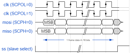
SPI Serial Format (SCPH = 0)
When SCPH = 0, data transmission starts from the falling edge of the slave select signal. During continuous data transfers, whether the SPI master’s slave select signal toggles before the next data frame can be configured through the SS_T field in the CTRLR0 register. Regardless of whether the master toggles the slave select signal during continuous data transfers, the SPI slave can communicate normally with the serial master. The timing diagrams for SS toggling and SS non-toggling are shown below. The SS toggling feature is used for compatibility with different SPI devices.
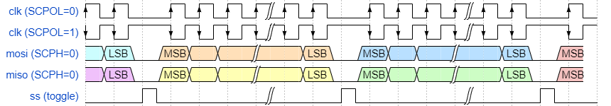
SPI Serial Format Continuous Transfers (SCPH = 0, SS Toggling)
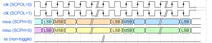
SPI Serial Format Continuous Transfers (SCPH = 0, SS Non-Toggling)
When the configuration parameter SCPH = 1, both master and slave peripherals begin transmitting data on the first serial clock edge after the slave select line is activated. The first data bit is captured on the second (trailing) serial clock edge. Data is propagated by the master and slave peripherals on the leading edge of the serial clock. During continuous data frame transfers, the slave select line can remain active low until the last bit of the last frame is captured. The figure below shows the timing diagram of the SPI format when SCPH = 1, with serial clock waveforms for both SCPOL = 0 and SCPOL = 1 configuration parameters.
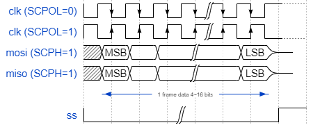
SPI Serial Format (SCPH = 1)
Continuous data frame transfers operate in the same manner as single-frame transfers, with the most significant bit (MSB) of the next frame immediately following the least significant bit (LSB) of the current frame. The slave select signal remains active throughout the entire transfer. The figure below shows the timing diagram of SPI continuous transfers when SCPH = 1.
SPI Serial Format Continuous Transfers (SCPH = 1, SS Non-Toggling)
SPI Serial Format Continuous Transfers (SCPH = 1, SS Toggling)
Data Format
Data Frame Length
The SPI controller supports a configurable data frame length of 4 to 16 bits, set through the DFS field of the CTRLR0 register. The reset default value is 8 bits.
Regardless of the configured DFS value, valid data in the FIFO is always right-aligned, with the upper bits automatically zero-padded. When software writes data to the DR register, the hardware automatically right-aligns the data. The transmit logic processes only the valid bits and ignores unused upper bits. The receive logic automatically right-aligns the serial input data before storing it into the receive FIFO, with the upper bits zero-padded.
Bit Order Swap
By default, the SPI controller transmits data on the serial line in MSB-first (most significant bit first) order. When LSB-first (least significant bit first) order is required, the bit order swap bits in the CTRLR0 register can be used to enable hardware-level automatic swapping on either the transmit or receive channel. Swapping operates on a per-FIFO-entry (16-bit) basis, independently bit-reversing the high byte [15:8] and the low byte [7:0]. No software per-bit processing is needed.
The transmit channel is controlled by TXBITSWAP (CTRLR0[22]), and the receive channel is controlled by RXBITSWAP (CTRLR0[24]). These two are independent of each other and can be configured separately according to external device requirements. Setting either bit to 0 means no swap (MSB first), while setting it to 1 means swap (LSB first).
Taking DFS = 8 as an example, writing 0x00B1 (low byte 10110001) to DR:
Configuration |
Bit Order Processing |
Output Data |
|---|---|---|
TXBITSWAP = 0 |
No swap (MSB first) |
10110001 (0xB1) |
TXBITSWAP = 1 |
Bit-reversed (LSB first) |
10001101 (0x8D) |
Note
Since bit order swapping operates on a full 16-bit FIFO entry, it is recommended to enable this feature only when DFS = 8 or DFS = 16. For other DFS values, the valid data bits are not an integer multiple of 8 or 16, so the hardware zero-pads the upper bits. Those zero-padded bits will be included in the swap operation, resulting in corruption of the valid data.
Byte Order Swap
The SPI controller supports separate byte order swap configuration for the transmit and receive channels. It swaps the high byte [15:8] and the low byte [7:0] of a 16-bit FIFO entry. Byte order swap is disabled by default. When the byte order needs to be changed, the byte order swap bits in the CTRLR0 register can be used to enable hardware-level automatic swapping without requiring software per-byte processing.
The transmit channel is controlled by TXBYTESWAP (CTRLR0[21]), and the receive channel is controlled by RXBYTESWAP (CTRLR0[23]). These two are independent of each other and can be configured separately according to external device requirements. Setting either bit to 0 means no swap (high byte first), while setting it to 1 means swap (low byte first).
Taking DFS = 16 as an example, writing 0xA569 (high byte 0xA5, low byte 0x69) to DR:
Configuration |
Byte Order Processing |
Output Data |
|---|---|---|
TXBYTESWAP = 0 |
No swap (high byte first) |
0xA5 → 0x69 |
TXBYTESWAP = 1 |
High/low byte swapped (low byte first) |
0x69 → 0xA5 |
Note
Since byte order swapping operates on a full 16-bit FIFO entry, it is recommended to enable this feature only when DFS = 16. When DFS < 16, the upper region is zero-padded. After byte swapping, the zero byte will be swapped into the low position, resulting in corrupted valid data.
Clock Configuration
When SPI is configured as a master, the maximum frequency of the serial clock (sclk_out) is half the frequency of the SPI peripheral clock (ssi_clk). This allows the shift control logic to capture data on one clock edge of sclk_out and propagate data on the other edge, as shown in the figure below. The sclk_out signal line toggles only during active data transfers. At all other times, it remains inactive, as defined by the serial protocol under which it operates.
The frequency of sclk_out can be derived from the following formula:
Fsclk_out= Fssi_clk/SCKDV
SCKDV is a bit field in the programmable register BAUDR, and can be set to any even value between 0 and 65534. If SCKDV is 0, sclk_out is disabled.

Maximum sclk_out/ssi_clk Ratio
The chip supports high-speed SPI slave. When SPI is configured as a slave, the maximum frequency of the serial clock (sclk_in) provided by the serial master can be up to half the ssi_clk frequency.
The frequency ratio constraints between the serial clock (sclk_out/sclk_in) and the SPI peripheral clock (ssi_clk) are summarized as follows:
Master: Fssi_clk>= 2 x (maximum Fsclk_out)
Slave: Fssi_clk>= 2 x (maximum Fsclk_in)
The Fssi_clkof SPI0 and SPI1 are identical, supporting up to 100 MHz.
Note
Fssi_clkis affected by the PLL (Phase-Locked Loop) configuration during the Bootloader stage.
Transfer Mode
When transmitting data on the serial bus, the SPI master can operate in multiple modes as described below. The transfer mode (TMOD) is configured by writing to control register 0 (CTRLR0).
When transmitting data on the serial bus, the SPI slave can only operate in full-duplex mode. That is, the TMOD field in the CTRLR0 register has no effect on the SPI slave. If the device is not expected to return data, slave output can be disabled via the SLV_OE bit in CTRLR0.
Full-Duplex Mode
When TMOD = 2'b00, both transmit and receive logic are active. Transmit data is popped from the transmit FIFO and sent to the target device via the MOSI line, while the target device returns data via the MISO line. Received data from the target device is shifted from the receive shift register into the receive FIFO at the end of each data frame.
Half-Duplex Transmit Only Mode
When TMOD = 2'b01, received data is invalid and should not be stored in the receive FIFO. Transmit data is popped from the transmit FIFO and sent to the target device via the MOSI line, while the target device returns data via the MISO line. At the end of the data frame, the receive shift register does not load newly received data into the receive FIFO. Data in the receive shift register will be overwritten during the next transfer. When entering this mode, interrupts from the receive logic should be masked.
Half-Duplex Receive Only Mode
When TMOD = 2'b10, transmit data is invalid. The MOSI output remains at a constant logic level during the transfer. Received data from the target device is shifted from the receive shift register into the receive FIFO at the end of each data frame. When entering this mode, interrupts from the transmit logic should be masked.
FIFO Management
Both the transmit and receive FIFO Buffer have a depth of 64. Since the serial specification defines the length of a single serial transfer (data frame) as 4 to 16 bits, the width is fixed at 16 bits. Each data entry in the FIFO Buffer contains one data frame.
Note
When SPI is disabled (SSI_EN = 0) or reset, the transmit and receive FIFO Buffer are cleared.
The transmit FIFO is loaded through APB write operations to the SPI data register (DR). Data is popped (removed) from the transmit FIFO by the shift control logic into the transmit shift register. When the number of entries in the FIFO is less than or equal to the FIFO threshold, the transmit FIFO generates a FIFO empty interrupt request (ssi_txe_intr). This threshold is set through the programmable register TXFTLR, which determines the FIFO entry level at which the interrupt is generated. This threshold can provide the processor with an early indication that the transmit FIFO is about to become empty. If an attempt is made to write data to a full transmit FIFO, a transmit FIFO overflow interrupt (ssi_txo_intr) is generated.
Data is popped from the receive FIFO through APB read operations to the SPI data register (DR). The receive FIFO is loaded by the receive shift register via the shift control logic. When the number of entries in the FIFO is greater than or equal to the FIFO threshold plus 1, the receive FIFO generates a FIFO full interrupt request (ssi_rxf_intr). This threshold is set through the programmable register RXFTLR, which determines the FIFO entry level at which the interrupt is generated.
This threshold can provide the processor with an early indication that the receive FIFO is about to become full. When the receive shift logic attempts to load data into a full receive FIFO, a receive FIFO overflow interrupt (ssi_rxo_intr) is generated, and the newly received data is lost. If an attempt is made to read from an empty receive FIFO, a receive FIFO underflow interrupt (ssi_rxu_intr) is generated. This alerts the processor that the read data is invalid.
Interrupt Handling
SPI supports combined interrupt requests and individual interrupt requests, and each interrupt can be masked. The combined interrupt request is the OR result of all other SPI interrupts after masking. System designers can choose to route individual interrupt requests or only the combined interrupt request to the interrupt controller.
Interrupt Description
The trigger conditions and clearing methods for each interrupt are described as follows:
Transmit FIFO Empty Interrupt (
ssi_txe_intr) – Asserted when the transmit FIFO is at or below its threshold, requiring service to prevent underflow. This threshold is set through a software-programmable register to determine the transmit FIFO entry level at which the interrupt is generated. This interrupt is automatically cleared by hardware when data is written to the transmit FIFO Buffer and raises it above the threshold level.Transmit FIFO Overflow Interrupt (
ssi_txo_intr) – Asserted when an APB access attempts to write data to a full transmit FIFO. When asserted, write data from the APB is discarded. This interrupt remains asserted until the Transmit FIFO Overflow Interrupt Clear Register (TXOICR) is read.Receive FIFO Underflow Interrupt (
ssi_rxu_intr) – Asserted when an APB access attempts to read data from an empty receive FIFO. When asserted, the data read back from the receive FIFO is zero. This interrupt remains asserted until the Receive FIFO Underflow Interrupt Clear Register (RXUICR) is read.Receive FIFO Overflow Interrupt (
ssi_rxo_intr) – Asserted when the receive logic attempts to put data into the receive FIFO when it is already full. When asserted, the newly received data is discarded. This interrupt remains asserted until the Receive FIFO Overflow Interrupt Clear Register (RXOICR) is read.Receive FIFO Full Interrupt (
ssi_rxf_intr) – Asserted when the receive FIFO is at or above its threshold plus 1, requiring service to prevent overflow. This threshold is set through a software-programmable register to determine the receive FIFO entry level at which the interrupt is generated. This interrupt is automatically cleared by hardware when data is read from the receive FIFO Buffer and drops it below the threshold level.Frame Alignment Error Interrupt (
ssi_fae_intr) – Valid only when SPI is configured as a serial slave device. This interrupt is asserted when the received data frame length does not match the DFS (Data Frame Size) setting in CTRLR0. This interrupt remains asserted until the Frame Alignment Error Interrupt Clear Register ( MSTICR_FAEICR ) is read.Multi-Master Contention Interrupt (
ssi_mst_intr) – Not supported at this time.Transmit FIFO Underflow Interrupt (
ssi_txu_intr) – Valid only when SPI is configured as a serial slave device. This interrupt is asserted when the transmit logic attempts to read data from an empty transmit FIFO. When asserted, the data transmitted by the slave device is invalid. This interrupt remains asserted until the Transmit FIFO Underflow Interrupt Clear Register (TXUICR) is read.SS_N Rising Edge Detection Interrupt (
ssi_ssr_intr) – Valid only when SPI is configured as a serial slave device. This interrupt is asserted when an SS_N rising edge is detected. This interrupt remains asserted until the SS_N Rising Edge Detection Interrupt Clear Register (SSRICR) is read.
Interrupt Masking
The SPI Interrupt Mask Register (SPI_IMR) controls whether each interrupt source is masked. Each mask bit corresponds to an interrupt source: setting it to 1 means unmasked (interrupt enabled), and setting it to 0 means masked (interrupt disabled). The mask bits are defined as follows:
Transmit FIFO Empty Interrupt Mask (SPI_BIT_TXEIM) – Controls the
ssi_txe_intrinterrupt.Transmit FIFO Overflow Interrupt Mask (SPI_BIT_TXOIM) – Controls the
ssi_txo_intrinterrupt.Receive FIFO Underflow Interrupt Mask (SPI_BIT_RXUIM) – Controls the
ssi_rxu_intrinterrupt.Receive FIFO Overflow Interrupt Mask (SPI_BIT_RXOIM) – Controls the
ssi_rxo_intrinterrupt.Receive FIFO Full Interrupt Mask (SPI_BIT_RXFIM) – Controls the
ssi_rxf_intrinterrupt.Multi-Master Contention/Frame Alignment Error Interrupt Mask (SPI_BIT_MSTIM_FAEIM) – When SPI is configured as master, controls the
ssi_mst_intrinterrupt; when SPI is configured as slave, controls thessi_fae_intrinterrupt.Transmit FIFO Underflow Interrupt Mask (SPI_BIT_TXUIM) – Valid only when SPI is configured as slave, controls the
ssi_txu_intrinterrupt.SS_N Rising Edge Detection Interrupt Mask (SPI_BIT_SSRIM) – Valid only when SPI is configured as slave, controls the
ssi_ssr_intrinterrupt.
Mode Selection
The chip uses two separate sets of circuits when operating as an SPI master or SPI slave. Therefore, the user must configure the SPI role before initializing the device. The relevant register descriptions are as follows.
REG_LSYSPLAT_CTRL
Size: 32
Address: 0x41008230
Read/write access: R/W
Bit |
Symbol |
Access |
INI |
Description |
|---|---|---|---|---|
27 |
SPI1_MST |
R/W |
0h |
|
26 |
SPI0_MST |
R/W |
0h |
|
REG_LSYSPLAT_CTRL
Size: 32
Address: 0x4100C230
Read/write access: R/W
Bit |
Symbol |
Access |
INI |
Description |
|---|---|---|---|---|
27 |
SPI1_MST |
R/W |
0h |
|
26 |
SPI0_MST |
R/W |
0h |
|
REG_LSYSPLAT_CTRL
Size: 32
Address: 0x4100C230
Read/write access: R/W
Bit |
Symbol |
Access |
INI |
Description |
|---|---|---|---|---|
27 |
SPI1_MST |
R/W |
0h |
|
26 |
SPI0_MST |
R/W |
0h |
|
REG_LSYSPLAT_CTRL
Size: 32
Address: 0x4100C230
Read/write access: R/W
Bit |
Symbol |
Access |
INI |
Description |
|---|---|---|---|---|
27 |
SPI1_MST |
R/W |
0h |
|
26 |
SPI0_MST |
R/W |
0h |
|
REG_LSYSPLAT_CTRL
Size: 32
Address: 0x4100C230
Read/write access: R/W
Bit |
Symbol |
Access |
INI |
Description |
|---|---|---|---|---|
27 |
SPI1_MST |
R/W |
0h |
|
26 |
SPI0_MST |
R/W |
0h |
|
REG_HSYSHPLAT_CTRL
Size: 32
Address: 0x41000030
Read/write access: R/W
Bit |
Symbol |
Access |
INI |
Description |
|---|---|---|---|---|
26 |
SPI1_MST |
R/W |
0h |
|
25 |
SPI0_MST |
R/W |
0h |
|
REG_LSYSPLAT_CTRL
Size: 32
Address: 0x4080A2A0
Read/write access: R/W
Bit |
Symbol |
Access |
INI |
Description |
|---|---|---|---|---|
27 |
SPI1_MST |
R/W |
0h |
|
26 |
SPI0_MST |
R/W |
0h |
|
REG_LSYSPLAT_CTRL
Size: 32
Address: 0x408012A0
Read/write access: R/W
Bit |
Symbol |
Access |
INI |
Description |
|---|---|---|---|---|
27 |
SPI1_MST |
R/W |
0h |
|
26 |
SPI0_MST |
R/W |
0h |
|
Master Mode
This mode implements serial communication with serial slave peripherals. When configured as a serial master, the SPI initiates and controls all serial transfers. This figure shows an example of the SPI configured as a serial master, with all other devices on the serial bus controlled by GPIO as slave select signals.
The serial clock generated and controlled by the SPI master is output through the sclk_out line. When the SPI is disabled (SSI_EN = 0), no serial transfers occur, and sclk_out remains inactive.
Transfer Control
Data transfers are initiated and controlled by the serial master, involving start, stop, and status phases.
Start
Before a transfer begins, the slave select signal must be driven low: if using the built-in slave select signal (hardware CS), it is automatically driven low by hardware; if using a GPIO to emulate the slave select signal (software CS), the user must manually control the GPIO to drive it low.
A transfer starts when three conditions are met: the SPI is enabled (SSI_EN=1), there is at least one valid data entry in the transmit FIFO, and a serial slave is selected. To ensure continuous transfer integrity, at least two data entries can be pre-written to the transmit FIFO before enabling the slave, so that the transfer begins only after sufficient data frames have accumulated in the FIFO.
For receive-only mode (TMOD = 2'b10), the startup method differs slightly: dummy data must be written to the transmit FIFO when selecting the slave to trigger the serial clock. During the transfer, the MOSI output maintains a constant logic level, and the transmit FIFO is popped only once at the start, after which it can remain empty.
The transmit FIFO threshold (TXFTLR) can generate an early interrupt (ssi_txe_intr) when the number of FIFO entries drops below the threshold, notifying the processor that the transmit FIFO is about to become empty. When using DMA, the transmit data level (DMATDLR) can issue an early request (dma_tx_req) to the DMA controller to replenish data in time and maintain continuous transfers.
The receive FIFO threshold (RXFTLR) can provide an early indication that the FIFO is about to become full when the number of entries reaches the threshold plus one. When using DMA, the receive data level (DMARDLR) can issue an early request (dma_rx_req) to the DMA controller to read data in time and prevent overflow.
Stop
The stop conditions under different transfer modes are as follows:
In full-duplex (transmit and receive) mode and simplex transmit-only mode (TMOD = 2'b00 or TMOD = 2'b01), the shift control logic terminates the transfer when the transmit FIFO is empty. Therefore, during continuous data transfers, ensure that the transmit FIFO does not become empty before all data has been transferred.
In simplex receive-only mode (TMOD = 2'b10), the transfer end is determined by the number of data frames (NDF) field in Control Register 1 (CTRLR1). When the number of received frames equals NDF + 1, the receive logic terminates the transfer. For example, to receive 24 frames, program NDF to 23. In this mode, the transmit FIFO does not need to be continuously serviced during the transfer, saving APB bandwidth, but data should be read promptly each time the receive FIFO generates a full interrupt to prevent overflow.
After the transfer completes, the slave select signal must be driven high: if using hardware CS, it is automatically driven high by hardware; if using software CS, the user must manually control the GPIO to drive it high.
Status
During SPI transfers, the busy flag (BUSY) in the status register (SPI_SR) indicates the current transfer status:
Set (1): Indicates the SPI is actively transferring data
Clear (0): Indicates the SPI is idle
Before initiating the next serial transfer, the BUSY flag must be checked and waited to be cleared.
Chip Select Control
Not supported.
Not supported.
Not supported.
Not supported.
Not supported.
Not supported.
In some scenarios, interrupts may not be serviced in time to fill the TX FIFO, causing it to become empty. Therefore, the CSF_EN bit in register CTRLR0 allows the SPI master to force the slave select signal to remain low until the entire transfer is complete. Additionally, during a transfer that has not yet completed, when the TX FIFO is empty, the SPI master keeps the CS signal low and pauses the transfer (without sending the sclk clock signal).
When the CSF_EN bit is enabled, the SPI master calculates the number of data bits to be transmitted. The calculation is the Data Frame Size (CTRLR0 [3:0]) multiplied by the Number of Data Frames (CTRLR1 [15:0]). Subsequently, the SPI master forces the slave select signal to remain low during the transfer. The SPI master releases this force control only when the number of transmitted data bits reaches the calculated value. An example of CSF_EN usage is shown below.
Receive Delayed Sampling
The slave uses the clock signal from the master as a strobe signal to drive data onto the MISO line. Due to round-trip routing delays in the clock signal, the slave’s data output may appear delayed from the master’s perspective, deviating from the normal sampling time. When the SPI is configured as a master, additional logic can be included to delay the default sampling time of the MISO signal, which helps increase the maximum achievable frequency on the serial bus.
The figure below shows an example of how routing delays on the MOSI signal can cause the master to sample incorrect MISO values at the default sampling time. The blue arrows represent the routing delays between the master and slave; the red lines represent the sampling delay from when the slave receives the clock to when it drives data output on the MISO line.
Effects of round-trip routing delays on the clock signal
When the RXD sampling delay logic is included, the delay value can be dynamically programmed to offset the sampling time of the rxd signal from the default by a number of pclk cycles.
The sampling delay logic has a resolution of one pclk cycle. Software can “calibrate” the serial bus by writing a loop that continuously reads from the slave and increments the master RXD sampling delay value until the master receives correct data.
Note
The maximum number of ssi_clk cycles available for delaying the rxd input sampling is 4. If the programmed delay value exceeds this maximum, zero (0) delay will be applied to the rxd sampling.
Slave Mode
This mode enables serial communication with a serial master peripheral. When the SPI is configured as a slave device, all serial transfers are initiated and controlled by the serial bus master.
The SPI slave can only operate in transmit-and-receive mode. That is, the TMOD field in the CTRLR0 register has no effect on the SPI slave. If the device is not expected to respond with data, slave output can be disabled through the SLV_OE bit in CTRLR0.
When the SPI serial slave is selected during configuration, it outputs MISO data onto the serial bus. All data transfers in and out of the serial slave are controlled by the serial clock line (sclk_in), which is driven by the serial master. Data is propagated from the serial slave on one edge of the serial clock line and sampled on the opposite edge.
When the SPI serial slave is not selected, it must not interfere with data transfers between the serial master and other serial slave devices. When the serial slave is not selected, its MISO output is buffered, presenting a high-impedance drive on the MISO line of the serial master.
The serial clock that regulates data transfers is generated by the serial master and input to the SPI slave via sclk_in. The slave remains idle until selected by the bus master. When not actively transferring data, the slave must keep its MISO line in a high-impedance state to avoid interfering with serial transfers to and from other slave devices. As long as the slave remains selected, it continues to transfer data to and from the master.
Transfer Control
If the SPI slave is to transmit data to the master, it must ensure that data is already present in the transmit FIFO before the serial master initiates a transfer. If the master initiates a transfer to the SPI slave when there is no data in the transmit FIFO, an error flag (TXE) is set in the SPI status register, and the previously transmitted data frame is retransmitted on MISO. For continuous data transfers, it is essential to ensure that the transmit FIFO buffer does not become empty before all data transfers are complete. The transmit FIFO threshold level register (TXFTLR) can be used to generate an early interrupt (ssi_txe_intr) to the processor, indicating that the transmit FIFO buffer is about to become empty. When using the DMA controller for APB access, the DMA transmit data level register (DMATDLR) can be used to generate an early request (dma_tx_req) to the DMA controller, indicating that the transmit FIFO is about to become empty. The FIFO can then be refilled with data to continue the serial transfer.
The receive FIFO buffer should be read each time a FIFO full interrupt request is generated by the receive FIFO to prevent overflow. The receive FIFO threshold level register (RXFTLR) can be used to provide an early indication that the receive FIFO is about to become full. When using the DMA controller for APB access, the DMA receive data level register (DMARDLR) can be used to generate an early request (dma_rx_req) to the DMA controller, indicating that the receive FIFO is about to become full.
DMA Support
SPI has an optional built-in DMA capability that can be selected during configuration. It provides a handshake interface with the DMA controller for requesting and controlling data transfers. The APB bus is used to perform data transfers to and from the DMA.
SPI uses two DMA channels: one for transmitting data and one for receiving data. SPI has the following DMA registers:
DMACR: Control register used to enable DMA operations.
DMATDLR: Transmit threshold register used to set the threshold of transmit FIFO data level that triggers a DMA request.
DMARDLR: Receive threshold register used to set the threshold of receive FIFO data level that triggers a DMA request.
To enable the DMA controller interface on SPI, the DMA Control Register (DMACR) must be written. Writing '1' to the TDMAE bit field of DMACR enables the SPI transmit handshake interface. Writing '1' to the RDMAE bit field of DMACR enables the SPI receive handshake interface.
Transmit Data Threshold and Transmit FIFO Underflow
During SPI serial transfer, a transmit FIFO request is sent to the DMA controller whenever the number of data entries in the transmit FIFO is less than or equal to the value of the DMA Transmit Data Level Register (DMATDLR). This value is referred to as the transmit data threshold. The DMA controller responds by writing a burst of data into the transmit FIFO buffer.
Data should be fetched from the DMA frequently enough to ensure that the transmit FIFO can sustain continuous serial transfer; that is, when the FIFO is about to become empty, another DMA request should be triggered in time. Otherwise, the FIFO will experience data starvation (underflow). To prevent this, the user must set the threshold correctly.
Receive Data Threshold and Receive FIFO Overflow
During SPI serial transfer, a receive FIFO request is sent to the DMA controller whenever the number of data entries in the receive FIFO reaches or exceeds the value of the DMA Receive Data Level Register, which is DMARDLR+1. This value is referred to as the receive data threshold. The DMA controller responds by fetching a burst of data from the receive FIFO buffer.
The DMA should fetch data frequently enough to ensure that the receive FIFO can continuously accept incoming serial data; that is, when the FIFO is about to become full, another DMA transfer should be requested in time. Otherwise, the FIFO will experience data overflow. To prevent this, the user must set the threshold correctly.
Registers
This section describes the programmable registers of the SPI. The following table provides the details of the SPI memory map. All registers in the SPI are addressed at 32-bit boundaries to remain consistent with the AHB bus. Where the physical size of any register is less than 32-bit wide, the upper unused bits of the 32-bit boundary are reserved. Writing to these bits has no effect; reading from these bits returns 0.
Base Address:
SPI0_REG : 0x40124000
SPI1_REG : 0x40125000
Name |
Address offset |
Access |
Description |
|---|---|---|---|
000h |
R/W |
This register controls the serial data transfer. It is impossible to write to this register when the SPI is enabled. The SPI is enabled and disabled by writing to the SSIENR register. |
|
004h |
R/W |
This register exists only when the SPI is configured as a master device. When the SPI is configured as a serial slave, writing to this location has no effect; reading from this location returns 0. Control register 1 controls the end of serial transfers when in receive-only mode. It is impossible to write to this register when the SPI is enabled. The SPI is enabled and disabled by writing to the SSIENR register. |
|
008h |
R/W |
This register enables and disables the SPI. |
|
010h |
R/W |
This register is valid only when the SPI is configured as a master device. When the SPI is configured as a serial slave, writing to this location has no effect; reading from this location returns 0. You cannot write to this register when SPI is busy. |
|
014h |
R/W |
This register is valid only when the SPI is configured as a master device. When the SPI is configured as a serial slave, writing to this location has no effect; reading from this location returns 0. The register derives the frequency of the serial clock that regulates the data transfer. The 16-bit field in this register defines the ssi_clk divider value. It is impossible to write to this register when the SPI is enabled. The SPI is enabled and disabled by writing to the SSIENR register. |
|
018h |
R/W |
This register controls the threshold value for the transmit FIFO memory. It is impossible to write to this register when the SPI is enabled. The SPI is enabled and disabled by writing to the SSIENR register. |
|
01Ch |
R/W |
This register controls the threshold value for the receive FIFO memory. It is impossible to write to this register when the SPI is enabled. The SPI is enabled and disabled by writing to the SSIENR register. |
|
020h |
R |
This register contains the number of valid data entries in the transmit FIFO memory. |
|
024h |
R |
This register contains the number of valid data entries in the receive FIFO memory. This register can be read at any time. |
|
028h |
R |
This is a read-only register used to indicate the current transfer status, FIFO status, and any transmission/reception errors that may have occurred. The status register may be read at any time. None of the bits in this register request an interrupt. |
|
02Ch |
R/W |
This read/write register masks or enables all interrupts generated by the SPI. |
|
030h |
R |
This register reports the status of the SPI interrupts after they have been masked. |
|
034h |
R |
This read-only register reports the status of the SPI interrupts prior to masking. |
|
038h |
R |
||
03Ch |
R |
||
040h |
R |
||
044h |
R |
Serial-master : MSTICR is not used because ss_in_n is tie 1 for Motorola-SPI, ssi_mst_intr is not used. |
|
048h |
R |
||
04Ch |
R/W |
This register is only valid when SPI is configured with a set of DMA Controller interface signals. |
|
050h |
R/W |
This register is only valid when the SPI is configured with a set of DMA interface signals. |
|
054h |
R/W |
This register is only valid when SPI is configured with a set of DMA interface signals. |
|
058h |
R |
This register is present only if SPI is configured as serial-slave. |
|
05Ch |
R |
This register is present only if SPI is configured as serial-slave. |
|
060h |
R/W |
The SPI data register is a 16-bit read/write buffer for the transmit/receive FIFOs. When the register is read, data in the receive FIFO buffer is accessed. When it is written to, data are moved into the transmit FIFO buffer; a write can occur only when SSI_EN = 1. FIFOs are reset when SSI_EN = 0. Note1: If the Data Register (DR) is accessed from an AHB master (such as a DMA controller or a processor), the AHB transfer type may be a burst. During AHB burst transfers, the address increments after each beat of the burst. To facilitate an AHB burst, read, or write operation to the transmit or receive FIFO, the Date Register occupies thirty-six 32-bit address locations of memory map. Each of the 16-bit address locations are aliased to the DR; single accesses to the DR may use any of the 16-bit address locations. Note2: The DR register in the SPI occupies thirty-six 32-bit address locations of the memory map to facilitate AHB burst transfers. Writing to any of these address locations has the same effect as pushing the data from the pwdata bus into the transmit FIFO. Reading from any of these locations has the same effect as popping data from the receive FIFO onto the prdata bus. The FIFO buffers on the SPI are not addressable. |
|
064h |
R/W |
The SPI data register is a 16-bit read/write buffer for the transmit/receive FIFOs. When the register is read, data in the receive FIFO buffer is accessed. When it is written to, data are moved into the transmit FIFO buffer; a write can occur only when SSI_EN = 1. FIFOs are reset when SSI_EN = 0. Note1: If the Data Register (DR) is accessed from an AHB master (such as a DMA controller or a processor), the AHB transfer type may be a burst. During AHB burst transfers, the address increments after each beat of the burst. To facilitate an AHB burst, read, or write operation to the transmit or receive FIFO, the Date Register occupies thirty-six 32-bit address locations of memory map. Each of the 16-bit address locations are aliased to the DR; single accesses to the DR may use any of the 16-bit address locations. Note2: The DR register in the SPI occupies thirty-six 32-bit address locations of the memory map to facilitate AHB burst transfers. Writing to any of these address locations has the same effect as pushing the data from the pwdata bus into the transmit FIFO. Reading from any of these locations has the same effect as popping data from the receive FIFO onto the prdata bus. The FIFO buffers on the SPI are not addressable. |
|
068h |
R/W |
The SPI data register is a 16-bit read/write buffer for the transmit/receive FIFOs. When the register is read, data in the receive FIFO buffer is accessed. When it is written to, data are moved into the transmit FIFO buffer; a write can occur only when SSI_EN = 1. FIFOs are reset when SSI_EN = 0. Note1: If the Data Register (DR) is accessed from an AHB master (such as a DMA controller or a processor), the AHB transfer type may be a burst. During AHB burst transfers, the address increments after each beat of the burst. To facilitate an AHB burst, read, or write operation to the transmit or receive FIFO, the Date Register occupies thirty-six 32-bit address locations of memory map. Each of the 16-bit address locations are aliased to the DR; single accesses to the DR may use any of the 16-bit address locations. Note2: The DR register in the SPI occupies thirty-six 32-bit address locations of the memory map to facilitate AHB burst transfers. Writing to any of these address locations has the same effect as pushing the data from the pwdata bus into the transmit FIFO. Reading from any of these locations has the same effect as popping data from the receive FIFO onto the prdata bus. The FIFO buffers on the SPI are not addressable. |
|
06Ch |
R/W |
The SPI data register is a 16-bit read/write buffer for the transmit/receive FIFOs. When the register is read, data in the receive FIFO buffer is accessed. When it is written to, data are moved into the transmit FIFO buffer; a write can occur only when SSI_EN = 1. FIFOs are reset when SSI_EN = 0. Note1: If the Data Register (DR) is accessed from an AHB master (such as a DMA controller or a processor), the AHB transfer type may be a burst. During AHB burst transfers, the address increments after each beat of the burst. To facilitate an AHB burst, read, or write operation to the transmit or receive FIFO, the Date Register occupies thirty-six 32-bit address locations of memory map. Each of the 16-bit address locations are aliased to the DR; single accesses to the DR may use any of the 16-bit address locations. Note2: The DR register in the SPI occupies thirty-six 32-bit address locations of the memory map to facilitate AHB burst transfers. Writing to any of these address locations has the same effect as pushing the data from the pwdata bus into the transmit FIFO. Reading from any of these locations has the same effect as popping data from the receive FIFO onto the prdata bus. The FIFO buffers on the SPI are not addressable. |
|
070h |
R/W |
The SPI data register is a 16-bit read/write buffer for the transmit/receive FIFOs. When the register is read, data in the receive FIFO buffer is accessed. When it is written to, data are moved into the transmit FIFO buffer; a write can occur only when SSI_EN = 1. FIFOs are reset when SSI_EN = 0. Note1: If the Data Register (DR) is accessed from an AHB master (such as a DMA controller or a processor), the AHB transfer type may be a burst. During AHB burst transfers, the address increments after each beat of the burst. To facilitate an AHB burst, read, or write operation to the transmit or receive FIFO, the Date Register occupies thirty-six 32-bit address locations of memory map. Each of the 16-bit address locations are aliased to the DR; single accesses to the DR may use any of the 16-bit address locations. Note2: The DR register in the SPI occupies thirty-six 32-bit address locations of the memory map to facilitate AHB burst transfers. Writing to any of these address locations has the same effect as pushing the data from the pwdata bus into the transmit FIFO. Reading from any of these locations has the same effect as popping data from the receive FIFO onto the prdata bus. The FIFO buffers on the SPI are not addressable. |
|
074h |
R/W |
The SPI data register is a 16-bit read/write buffer for the transmit/receive FIFOs. When the register is read, data in the receive FIFO buffer is accessed. When it is written to, data are moved into the transmit FIFO buffer; a write can occur only when SSI_EN = 1. FIFOs are reset when SSI_EN = 0. Note1: If the Data Register (DR) is accessed from an AHB master (such as a DMA controller or a processor), the AHB transfer type may be a burst. During AHB burst transfers, the address increments after each beat of the burst. To facilitate an AHB burst, read, or write operation to the transmit or receive FIFO, the Date Register occupies thirty-six 32-bit address locations of memory map. Each of the 16-bit address locations are aliased to the DR; single accesses to the DR may use any of the 16-bit address locations. Note2: The DR register in the SPI occupies thirty-six 32-bit address locations of the memory map to facilitate AHB burst transfers. Writing to any of these address locations has the same effect as pushing the data from the pwdata bus into the transmit FIFO. Reading from any of these locations has the same effect as popping data from the receive FIFO onto the prdata bus. The FIFO buffers on the SPI are not addressable. |
|
078h |
R/W |
The SPI data register is a 16-bit read/write buffer for the transmit/receive FIFOs. When the register is read, data in the receive FIFO buffer is accessed. When it is written to, data are moved into the transmit FIFO buffer; a write can occur only when SSI_EN = 1. FIFOs are reset when SSI_EN = 0. Note1: If the Data Register (DR) is accessed from an AHB master (such as a DMA controller or a processor), the AHB transfer type may be a burst. During AHB burst transfers, the address increments after each beat of the burst. To facilitate an AHB burst, read, or write operation to the transmit or receive FIFO, the Date Register occupies thirty-six 32-bit address locations of memory map. Each of the 16-bit address locations are aliased to the DR; single accesses to the DR may use any of the 16-bit address locations. Note2: The DR register in the SPI occupies thirty-six 32-bit address locations of the memory map to facilitate AHB burst transfers. Writing to any of these address locations has the same effect as pushing the data from the pwdata bus into the transmit FIFO. Reading from any of these locations has the same effect as popping data from the receive FIFO onto the prdata bus. The FIFO buffers on the SPI are not addressable. |
|
07Ch |
R/W |
The SPI data register is a 16-bit read/write buffer for the transmit/receive FIFOs. When the register is read, data in the receive FIFO buffer is accessed. When it is written to, data are moved into the transmit FIFO buffer; a write can occur only when SSI_EN = 1. FIFOs are reset when SSI_EN = 0. Note1: If the Data Register (DR) is accessed from an AHB master (such as a DMA controller or a processor), the AHB transfer type may be a burst. During AHB burst transfers, the address increments after each beat of the burst. To facilitate an AHB burst, read, or write operation to the transmit or receive FIFO, the Date Register occupies thirty-six 32-bit address locations of memory map. Each of the 16-bit address locations are aliased to the DR; single accesses to the DR may use any of the 16-bit address locations. Note2: The DR register in the SPI occupies thirty-six 32-bit address locations of the memory map to facilitate AHB burst transfers. Writing to any of these address locations has the same effect as pushing the data from the pwdata bus into the transmit FIFO. Reading from any of these locations has the same effect as popping data from the receive FIFO onto the prdata bus. The FIFO buffers on the SPI are not addressable. |
|
080h |
R/W |
The SPI data register is a 16-bit read/write buffer for the transmit/receive FIFOs. When the register is read, data in the receive FIFO buffer is accessed. When it is written to, data are moved into the transmit FIFO buffer; a write can occur only when SSI_EN = 1. FIFOs are reset when SSI_EN = 0. Note1: If the Data Register (DR) is accessed from an AHB master (such as a DMA controller or a processor), the AHB transfer type may be a burst. During AHB burst transfers, the address increments after each beat of the burst. To facilitate an AHB burst, read, or write operation to the transmit or receive FIFO, the Date Register occupies thirty-six 32-bit address locations of memory map. Each of the 16-bit address locations are aliased to the DR; single accesses to the DR may use any of the 16-bit address locations. Note2: The DR register in the SPI occupies thirty-six 32-bit address locations of the memory map to facilitate AHB burst transfers. Writing to any of these address locations has the same effect as pushing the data from the pwdata bus into the transmit FIFO. Reading from any of these locations has the same effect as popping data from the receive FIFO onto the prdata bus. The FIFO buffers on the SPI are not addressable. |
|
084h |
R/W |
The SPI data register is a 16-bit read/write buffer for the transmit/receive FIFOs. When the register is read, data in the receive FIFO buffer is accessed. When it is written to, data are moved into the transmit FIFO buffer; a write can occur only when SSI_EN = 1. FIFOs are reset when SSI_EN = 0. Note1: If the Data Register (DR) is accessed from an AHB master (such as a DMA controller or a processor), the AHB transfer type may be a burst. During AHB burst transfers, the address increments after each beat of the burst. To facilitate an AHB burst, read, or write operation to the transmit or receive FIFO, the Date Register occupies thirty-six 32-bit address locations of memory map. Each of the 16-bit address locations are aliased to the DR; single accesses to the DR may use any of the 16-bit address locations. Note2: The DR register in the SPI occupies thirty-six 32-bit address locations of the memory map to facilitate AHB burst transfers. Writing to any of these address locations has the same effect as pushing the data from the pwdata bus into the transmit FIFO. Reading from any of these locations has the same effect as popping data from the receive FIFO onto the prdata bus. The FIFO buffers on the SPI are not addressable. |
|
088h |
R/W |
The SPI data register is a 16-bit read/write buffer for the transmit/receive FIFOs. When the register is read, data in the receive FIFO buffer is accessed. When it is written to, data are moved into the transmit FIFO buffer; a write can occur only when SSI_EN = 1. FIFOs are reset when SSI_EN = 0. Note1: If the Data Register (DR) is accessed from an AHB master (such as a DMA controller or a processor), the AHB transfer type may be a burst. During AHB burst transfers, the address increments after each beat of the burst. To facilitate an AHB burst, read, or write operation to the transmit or receive FIFO, the Date Register occupies thirty-six 32-bit address locations of memory map. Each of the 16-bit address locations are aliased to the DR; single accesses to the DR may use any of the 16-bit address locations. Note2: The DR register in the SPI occupies thirty-six 32-bit address locations of the memory map to facilitate AHB burst transfers. Writing to any of these address locations has the same effect as pushing the data from the pwdata bus into the transmit FIFO. Reading from any of these locations has the same effect as popping data from the receive FIFO onto the prdata bus. The FIFO buffers on the SPI are not addressable. |
|
08Ch |
R/W |
The SPI data register is a 16-bit read/write buffer for the transmit/receive FIFOs. When the register is read, data in the receive FIFO buffer is accessed. When it is written to, data are moved into the transmit FIFO buffer; a write can occur only when SSI_EN = 1. FIFOs are reset when SSI_EN = 0. Note1: If the Data Register (DR) is accessed from an AHB master (such as a DMA controller or a processor), the AHB transfer type may be a burst. During AHB burst transfers, the address increments after each beat of the burst. To facilitate an AHB burst, read, or write operation to the transmit or receive FIFO, the Date Register occupies thirty-six 32-bit address locations of memory map. Each of the 16-bit address locations are aliased to the DR; single accesses to the DR may use any of the 16-bit address locations. Note2: The DR register in the SPI occupies thirty-six 32-bit address locations of the memory map to facilitate AHB burst transfers. Writing to any of these address locations has the same effect as pushing the data from the pwdata bus into the transmit FIFO. Reading from any of these locations has the same effect as popping data from the receive FIFO onto the prdata bus. The FIFO buffers on the SPI are not addressable. |
|
090h |
R/W |
The SPI data register is a 16-bit read/write buffer for the transmit/receive FIFOs. When the register is read, data in the receive FIFO buffer is accessed. When it is written to, data are moved into the transmit FIFO buffer; a write can occur only when SSI_EN = 1. FIFOs are reset when SSI_EN = 0. Note1: If the Data Register (DR) is accessed from an AHB master (such as a DMA controller or a processor), the AHB transfer type may be a burst. During AHB burst transfers, the address increments after each beat of the burst. To facilitate an AHB burst, read, or write operation to the transmit or receive FIFO, the Date Register occupies thirty-six 32-bit address locations of memory map. Each of the 16-bit address locations are aliased to the DR; single accesses to the DR may use any of the 16-bit address locations. Note2: The DR register in the SPI occupies thirty-six 32-bit address locations of the memory map to facilitate AHB burst transfers. Writing to any of these address locations has the same effect as pushing the data from the pwdata bus into the transmit FIFO. Reading from any of these locations has the same effect as popping data from the receive FIFO onto the prdata bus. The FIFO buffers on the SPI are not addressable. |
|
094h |
R/W |
The SPI data register is a 16-bit read/write buffer for the transmit/receive FIFOs. When the register is read, data in the receive FIFO buffer is accessed. When it is written to, data are moved into the transmit FIFO buffer; a write can occur only when SSI_EN = 1. FIFOs are reset when SSI_EN = 0. Note1: If the Data Register (DR) is accessed from an AHB master (such as a DMA controller or a processor), the AHB transfer type may be a burst. During AHB burst transfers, the address increments after each beat of the burst. To facilitate an AHB burst, read, or write operation to the transmit or receive FIFO, the Date Register occupies thirty-six 32-bit address locations of memory map. Each of the 16-bit address locations are aliased to the DR; single accesses to the DR may use any of the 16-bit address locations. Note2: The DR register in the SPI occupies thirty-six 32-bit address locations of the memory map to facilitate AHB burst transfers. Writing to any of these address locations has the same effect as pushing the data from the pwdata bus into the transmit FIFO. Reading from any of these locations has the same effect as popping data from the receive FIFO onto the prdata bus. The FIFO buffers on the SPI are not addressable. |
|
098h |
R/W |
The SPI data register is a 16-bit read/write buffer for the transmit/receive FIFOs. When the register is read, data in the receive FIFO buffer is accessed. When it is written to, data are moved into the transmit FIFO buffer; a write can occur only when SSI_EN = 1. FIFOs are reset when SSI_EN = 0. Note1: If the Data Register (DR) is accessed from an AHB master (such as a DMA controller or a processor), the AHB transfer type may be a burst. During AHB burst transfers, the address increments after each beat of the burst. To facilitate an AHB burst, read, or write operation to the transmit or receive FIFO, the Date Register occupies thirty-six 32-bit address locations of memory map. Each of the 16-bit address locations are aliased to the DR; single accesses to the DR may use any of the 16-bit address locations. Note2: The DR register in the SPI occupies thirty-six 32-bit address locations of the memory map to facilitate AHB burst transfers. Writing to any of these address locations has the same effect as pushing the data from the pwdata bus into the transmit FIFO. Reading from any of these locations has the same effect as popping data from the receive FIFO onto the prdata bus. The FIFO buffers on the SPI are not addressable. |
|
09Ch |
R/W |
The SPI data register is a 16-bit read/write buffer for the transmit/receive FIFOs. When the register is read, data in the receive FIFO buffer is accessed. When it is written to, data are moved into the transmit FIFO buffer; a write can occur only when SSI_EN = 1. FIFOs are reset when SSI_EN = 0. Note1: If the Data Register (DR) is accessed from an AHB master (such as a DMA controller or a processor), the AHB transfer type may be a burst. During AHB burst transfers, the address increments after each beat of the burst. To facilitate an AHB burst, read, or write operation to the transmit or receive FIFO, the Date Register occupies thirty-six 32-bit address locations of memory map. Each of the 16-bit address locations are aliased to the DR; single accesses to the DR may use any of the 16-bit address locations. Note2: The DR register in the SPI occupies thirty-six 32-bit address locations of the memory map to facilitate AHB burst transfers. Writing to any of these address locations has the same effect as pushing the data from the pwdata bus into the transmit FIFO. Reading from any of these locations has the same effect as popping data from the receive FIFO onto the prdata bus. The FIFO buffers on the SPI are not addressable. |
|
0A0h |
R/W |
The SPI data register is a 16-bit read/write buffer for the transmit/receive FIFOs. When the register is read, data in the receive FIFO buffer is accessed. When it is written to, data are moved into the transmit FIFO buffer; a write can occur only when SSI_EN = 1. FIFOs are reset when SSI_EN = 0. Note1: If the Data Register (DR) is accessed from an AHB master (such as a DMA controller or a processor), the AHB transfer type may be a burst. During AHB burst transfers, the address increments after each beat of the burst. To facilitate an AHB burst, read, or write operation to the transmit or receive FIFO, the Date Register occupies thirty-six 32-bit address locations of memory map. Each of the 16-bit address locations are aliased to the DR; single accesses to the DR may use any of the 16-bit address locations. Note2: The DR register in the SPI occupies thirty-six 32-bit address locations of the memory map to facilitate AHB burst transfers. Writing to any of these address locations has the same effect as pushing the data from the pwdata bus into the transmit FIFO. Reading from any of these locations has the same effect as popping data from the receive FIFO onto the prdata bus. The FIFO buffers on the SPI are not addressable. |
|
0A4h |
R/W |
The SPI data register is a 16-bit read/write buffer for the transmit/receive FIFOs. When the register is read, data in the receive FIFO buffer is accessed. When it is written to, data are moved into the transmit FIFO buffer; a write can occur only when SSI_EN = 1. FIFOs are reset when SSI_EN = 0. Note1: If the Data Register (DR) is accessed from an AHB master (such as a DMA controller or a processor), the AHB transfer type may be a burst. During AHB burst transfers, the address increments after each beat of the burst. To facilitate an AHB burst, read, or write operation to the transmit or receive FIFO, the Date Register occupies thirty-six 32-bit address locations of memory map. Each of the 16-bit address locations are aliased to the DR; single accesses to the DR may use any of the 16-bit address locations. Note2: The DR register in the SPI occupies thirty-six 32-bit address locations of the memory map to facilitate AHB burst transfers. Writing to any of these address locations has the same effect as pushing the data from the pwdata bus into the transmit FIFO. Reading from any of these locations has the same effect as popping data from the receive FIFO onto the prdata bus. The FIFO buffers on the SPI are not addressable. |
|
0A8h |
R/W |
The SPI data register is a 16-bit read/write buffer for the transmit/receive FIFOs. When the register is read, data in the receive FIFO buffer is accessed. When it is written to, data are moved into the transmit FIFO buffer; a write can occur only when SSI_EN = 1. FIFOs are reset when SSI_EN = 0. Note1: If the Data Register (DR) is accessed from an AHB master (such as a DMA controller or a processor), the AHB transfer type may be a burst. During AHB burst transfers, the address increments after each beat of the burst. To facilitate an AHB burst, read, or write operation to the transmit or receive FIFO, the Date Register occupies thirty-six 32-bit address locations of memory map. Each of the 16-bit address locations are aliased to the DR; single accesses to the DR may use any of the 16-bit address locations. Note2: The DR register in the SPI occupies thirty-six 32-bit address locations of the memory map to facilitate AHB burst transfers. Writing to any of these address locations has the same effect as pushing the data from the pwdata bus into the transmit FIFO. Reading from any of these locations has the same effect as popping data from the receive FIFO onto the prdata bus. The FIFO buffers on the SPI are not addressable. |
|
0ACh |
R/W |
The SPI data register is a 16-bit read/write buffer for the transmit/receive FIFOs. When the register is read, data in the receive FIFO buffer is accessed. When it is written to, data are moved into the transmit FIFO buffer; a write can occur only when SSI_EN = 1. FIFOs are reset when SSI_EN = 0. Note1: If the Data Register (DR) is accessed from an AHB master (such as a DMA controller or a processor), the AHB transfer type may be a burst. During AHB burst transfers, the address increments after each beat of the burst. To facilitate an AHB burst, read, or write operation to the transmit or receive FIFO, the Date Register occupies thirty-six 32-bit address locations of memory map. Each of the 16-bit address locations are aliased to the DR; single accesses to the DR may use any of the 16-bit address locations. Note2: The DR register in the SPI occupies thirty-six 32-bit address locations of the memory map to facilitate AHB burst transfers. Writing to any of these address locations has the same effect as pushing the data from the pwdata bus into the transmit FIFO. Reading from any of these locations has the same effect as popping data from the receive FIFO onto the prdata bus. The FIFO buffers on the SPI are not addressable. |
|
0B0h |
R/W |
The SPI data register is a 16-bit read/write buffer for the transmit/receive FIFOs. When the register is read, data in the receive FIFO buffer is accessed. When it is written to, data are moved into the transmit FIFO buffer; a write can occur only when SSI_EN = 1. FIFOs are reset when SSI_EN = 0. Note1: If the Data Register (DR) is accessed from an AHB master (such as a DMA controller or a processor), the AHB transfer type may be a burst. During AHB burst transfers, the address increments after each beat of the burst. To facilitate an AHB burst, read, or write operation to the transmit or receive FIFO, the Date Register occupies thirty-six 32-bit address locations of memory map. Each of the 16-bit address locations are aliased to the DR; single accesses to the DR may use any of the 16-bit address locations. Note2: The DR register in the SPI occupies thirty-six 32-bit address locations of the memory map to facilitate AHB burst transfers. Writing to any of these address locations has the same effect as pushing the data from the pwdata bus into the transmit FIFO. Reading from any of these locations has the same effect as popping data from the receive FIFO onto the prdata bus. The FIFO buffers on the SPI are not addressable. |
|
0B4h |
R/W |
The SPI data register is a 16-bit read/write buffer for the transmit/receive FIFOs. When the register is read, data in the receive FIFO buffer is accessed. When it is written to, data are moved into the transmit FIFO buffer; a write can occur only when SSI_EN = 1. FIFOs are reset when SSI_EN = 0. Note1: If the Data Register (DR) is accessed from an AHB master (such as a DMA controller or a processor), the AHB transfer type may be a burst. During AHB burst transfers, the address increments after each beat of the burst. To facilitate an AHB burst, read, or write operation to the transmit or receive FIFO, the Date Register occupies thirty-six 32-bit address locations of memory map. Each of the 16-bit address locations are aliased to the DR; single accesses to the DR may use any of the 16-bit address locations. Note2: The DR register in the SPI occupies thirty-six 32-bit address locations of the memory map to facilitate AHB burst transfers. Writing to any of these address locations has the same effect as pushing the data from the pwdata bus into the transmit FIFO. Reading from any of these locations has the same effect as popping data from the receive FIFO onto the prdata bus. The FIFO buffers on the SPI are not addressable. |
|
0BCh |
R/W |
The SPI data register is a 16-bit read/write buffer for the transmit/receive FIFOs. When the register is read, data in the receive FIFO buffer is accessed. When it is written to, data are moved into the transmit FIFO buffer; a write can occur only when SSI_EN = 1. FIFOs are reset when SSI_EN = 0. Note1: If the Data Register (DR) is accessed from an AHB master (such as a DMA controller or a processor), the AHB transfer type may be a burst. During AHB burst transfers, the address increments after each beat of the burst. To facilitate an AHB burst, read, or write operation to the transmit or receive FIFO, the Date Register occupies thirty-six 32-bit address locations of memory map. Each of the 16-bit address locations are aliased to the DR; single accesses to the DR may use any of the 16-bit address locations. Note2: The DR register in the SPI occupies thirty-six 32-bit address locations of the memory map to facilitate AHB burst transfers. Writing to any of these address locations has the same effect as pushing the data from the pwdata bus into the transmit FIFO. Reading from any of these locations has the same effect as popping data from the receive FIFO onto the prdata bus. The FIFO buffers on the SPI are not addressable. |
|
0C0h |
R/W |
The SPI data register is a 16-bit read/write buffer for the transmit/receive FIFOs. When the register is read, data in the receive FIFO buffer is accessed. When it is written to, data are moved into the transmit FIFO buffer; a write can occur only when SSI_EN = 1. FIFOs are reset when SSI_EN = 0. Note1: If the Data Register (DR) is accessed from an AHB master (such as a DMA controller or a processor), the AHB transfer type may be a burst. During AHB burst transfers, the address increments after each beat of the burst. To facilitate an AHB burst, read, or write operation to the transmit or receive FIFO, the Date Register occupies thirty-six 32-bit address locations of memory map. Each of the 16-bit address locations are aliased to the DR; single accesses to the DR may use any of the 16-bit address locations. Note2: The DR register in the SPI occupies thirty-six 32-bit address locations of the memory map to facilitate AHB burst transfers. Writing to any of these address locations has the same effect as pushing the data from the pwdata bus into the transmit FIFO. Reading from any of these locations has the same effect as popping data from the receive FIFO onto the prdata bus. The FIFO buffers on the SPI are not addressable. |
|
0C4h |
R/W |
The SPI data register is a 16-bit read/write buffer for the transmit/receive FIFOs. When the register is read, data in the receive FIFO buffer is accessed. When it is written to, data are moved into the transmit FIFO buffer; a write can occur only when SSI_EN = 1. FIFOs are reset when SSI_EN = 0. Note1: If the Data Register (DR) is accessed from an AHB master (such as a DMA controller or a processor), the AHB transfer type may be a burst. During AHB burst transfers, the address increments after each beat of the burst. To facilitate an AHB burst, read, or write operation to the transmit or receive FIFO, the Date Register occupies thirty-six 32-bit address locations of memory map. Each of the 16-bit address locations are aliased to the DR; single accesses to the DR may use any of the 16-bit address locations. Note2: The DR register in the SPI occupies thirty-six 32-bit address locations of the memory map to facilitate AHB burst transfers. Writing to any of these address locations has the same effect as pushing the data from the pwdata bus into the transmit FIFO. Reading from any of these locations has the same effect as popping data from the receive FIFO onto the prdata bus. The FIFO buffers on the SPI are not addressable. |
|
0C8h |
R/W |
The SPI data register is a 16-bit read/write buffer for the transmit/receive FIFOs. When the register is read, data in the receive FIFO buffer is accessed. When it is written to, data are moved into the transmit FIFO buffer; a write can occur only when SSI_EN = 1. FIFOs are reset when SSI_EN = 0. Note1: If the Data Register (DR) is accessed from an AHB master (such as a DMA controller or a processor), the AHB transfer type may be a burst. During AHB burst transfers, the address increments after each beat of the burst. To facilitate an AHB burst, read, or write operation to the transmit or receive FIFO, the Date Register occupies thirty-six 32-bit address locations of memory map. Each of the 16-bit address locations are aliased to the DR; single accesses to the DR may use any of the 16-bit address locations. Note2: The DR register in the SPI occupies thirty-six 32-bit address locations of the memory map to facilitate AHB burst transfers. Writing to any of these address locations has the same effect as pushing the data from the pwdata bus into the transmit FIFO. Reading from any of these locations has the same effect as popping data from the receive FIFO onto the prdata bus. The FIFO buffers on the SPI are not addressable. |
|
0CCh |
R/W |
The SPI data register is a 16-bit read/write buffer for the transmit/receive FIFOs. When the register is read, data in the receive FIFO buffer is accessed. When it is written to, data are moved into the transmit FIFO buffer; a write can occur only when SSI_EN = 1. FIFOs are reset when SSI_EN = 0. Note1: If the Data Register (DR) is accessed from an AHB master (such as a DMA controller or a processor), the AHB transfer type may be a burst. During AHB burst transfers, the address increments after each beat of the burst. To facilitate an AHB burst, read, or write operation to the transmit or receive FIFO, the Date Register occupies thirty-six 32-bit address locations of memory map. Each of the 16-bit address locations are aliased to the DR; single accesses to the DR may use any of the 16-bit address locations. Note2: The DR register in the SPI occupies thirty-six 32-bit address locations of the memory map to facilitate AHB burst transfers. Writing to any of these address locations has the same effect as pushing the data from the pwdata bus into the transmit FIFO. Reading from any of these locations has the same effect as popping data from the receive FIFO onto the prdata bus. The FIFO buffers on the SPI are not addressable. |
|
0D0h |
R/W |
The SPI data register is a 16-bit read/write buffer for the transmit/receive FIFOs. When the register is read, data in the receive FIFO buffer is accessed. When it is written to, data are moved into the transmit FIFO buffer; a write can occur only when SSI_EN = 1. FIFOs are reset when SSI_EN = 0. Note1: If the Data Register (DR) is accessed from an AHB master (such as a DMA controller or a processor), the AHB transfer type may be a burst. During AHB burst transfers, the address increments after each beat of the burst. To facilitate an AHB burst, read, or write operation to the transmit or receive FIFO, the Date Register occupies thirty-six 32-bit address locations of memory map. Each of the 16-bit address locations are aliased to the DR; single accesses to the DR may use any of the 16-bit address locations. Note2: The DR register in the SPI occupies thirty-six 32-bit address locations of the memory map to facilitate AHB burst transfers. Writing to any of these address locations has the same effect as pushing the data from the pwdata bus into the transmit FIFO. Reading from any of these locations has the same effect as popping data from the receive FIFO onto the prdata bus. The FIFO buffers on the SPI are not addressable. |
|
0D4h |
R/W |
The SPI data register is a 16-bit read/write buffer for the transmit/receive FIFOs. When the register is read, data in the receive FIFO buffer is accessed. When it is written to, data are moved into the transmit FIFO buffer; a write can occur only when SSI_EN = 1. FIFOs are reset when SSI_EN = 0. Note1: If the Data Register (DR) is accessed from an AHB master (such as a DMA controller or a processor), the AHB transfer type may be a burst. During AHB burst transfers, the address increments after each beat of the burst. To facilitate an AHB burst, read, or write operation to the transmit or receive FIFO, the Date Register occupies thirty-six 32-bit address locations of memory map. Each of the 16-bit address locations are aliased to the DR; single accesses to the DR may use any of the 16-bit address locations. Note2: The DR register in the SPI occupies thirty-six 32-bit address locations of the memory map to facilitate AHB burst transfers. Writing to any of these address locations has the same effect as pushing the data from the pwdata bus into the transmit FIFO. Reading from any of these locations has the same effect as popping data from the receive FIFO onto the prdata bus. The FIFO buffers on the SPI are not addressable. |
|
0D8h |
R/W |
The SPI data register is a 16-bit read/write buffer for the transmit/receive FIFOs. When the register is read, data in the receive FIFO buffer is accessed. When it is written to, data are moved into the transmit FIFO buffer; a write can occur only when SSI_EN = 1. FIFOs are reset when SSI_EN = 0. Note1: If the Data Register (DR) is accessed from an AHB master (such as a DMA controller or a processor), the AHB transfer type may be a burst. During AHB burst transfers, the address increments after each beat of the burst. To facilitate an AHB burst, read, or write operation to the transmit or receive FIFO, the Date Register occupies thirty-six 32-bit address locations of memory map. Each of the 16-bit address locations are aliased to the DR; single accesses to the DR may use any of the 16-bit address locations. Note2: The DR register in the SPI occupies thirty-six 32-bit address locations of the memory map to facilitate AHB burst transfers. Writing to any of these address locations has the same effect as pushing the data from the pwdata bus into the transmit FIFO. Reading from any of these locations has the same effect as popping data from the receive FIFO onto the prdata bus. The FIFO buffers on the SPI are not addressable. |
|
0DCh |
R/W |
The SPI data register is a 16-bit read/write buffer for the transmit/receive FIFOs. When the register is read, data in the receive FIFO buffer is accessed. When it is written to, data are moved into the transmit FIFO buffer; a write can occur only when SSI_EN = 1. FIFOs are reset when SSI_EN = 0. Note1: If the Data Register (DR) is accessed from an AHB master (such as a DMA controller or a processor), the AHB transfer type may be a burst. During AHB burst transfers, the address increments after each beat of the burst. To facilitate an AHB burst, read, or write operation to the transmit or receive FIFO, the Date Register occupies thirty-six 32-bit address locations of memory map. Each of the 16-bit address locations are aliased to the DR; single accesses to the DR may use any of the 16-bit address locations. Note2: The DR register in the SPI occupies thirty-six 32-bit address locations of the memory map to facilitate AHB burst transfers. Writing to any of these address locations has the same effect as pushing the data from the pwdata bus into the transmit FIFO. Reading from any of these locations has the same effect as popping data from the receive FIFO onto the prdata bus. The FIFO buffers on the SPI are not addressable. |
|
0E0h |
R/W |
The SPI data register is a 16-bit read/write buffer for the transmit/receive FIFOs. When the register is read, data in the receive FIFO buffer is accessed. When it is written to, data are moved into the transmit FIFO buffer; a write can occur only when SSI_EN = 1. FIFOs are reset when SSI_EN = 0. Note1: If the Data Register (DR) is accessed from an AHB master (such as a DMA controller or a processor), the AHB transfer type may be a burst. During AHB burst transfers, the address increments after each beat of the burst. To facilitate an AHB burst, read, or write operation to the transmit or receive FIFO, the Date Register occupies thirty-six 32-bit address locations of memory map. Each of the 16-bit address locations are aliased to the DR; single accesses to the DR may use any of the 16-bit address locations. Note2: The DR register in the SPI occupies thirty-six 32-bit address locations of the memory map to facilitate AHB burst transfers. Writing to any of these address locations has the same effect as pushing the data from the pwdata bus into the transmit FIFO. Reading from any of these locations has the same effect as popping data from the receive FIFO onto the prdata bus. The FIFO buffers on the SPI are not addressable. |
|
0E4h |
R/W |
The SPI data register is a 16-bit read/write buffer for the transmit/receive FIFOs. When the register is read, data in the receive FIFO buffer is accessed. When it is written to, data are moved into the transmit FIFO buffer; a write can occur only when SSI_EN = 1. FIFOs are reset when SSI_EN = 0. Note1: If the Data Register (DR) is accessed from an AHB master (such as a DMA controller or a processor), the AHB transfer type may be a burst. During AHB burst transfers, the address increments after each beat of the burst. To facilitate an AHB burst, read, or write operation to the transmit or receive FIFO, the Date Register occupies thirty-six 32-bit address locations of memory map. Each of the 16-bit address locations are aliased to the DR; single accesses to the DR may use any of the 16-bit address locations. Note2: The DR register in the SPI occupies thirty-six 32-bit address locations of the memory map to facilitate AHB burst transfers. Writing to any of these address locations has the same effect as pushing the data from the pwdata bus into the transmit FIFO. Reading from any of these locations has the same effect as popping data from the receive FIFO onto the prdata bus. The FIFO buffers on the SPI are not addressable. |
|
0E8h |
R/W |
The SPI data register is a 16-bit read/write buffer for the transmit/receive FIFOs. When the register is read, data in the receive FIFO buffer is accessed. When it is written to, data are moved into the transmit FIFO buffer; a write can occur only when SSI_EN = 1. FIFOs are reset when SSI_EN = 0. Note1: If the Data Register (DR) is accessed from an AHB master (such as a DMA controller or a processor), the AHB transfer type may be a burst. During AHB burst transfers, the address increments after each beat of the burst. To facilitate an AHB burst, read, or write operation to the transmit or receive FIFO, the Date Register occupies thirty-six 32-bit address locations of memory map. Each of the 16-bit address locations are aliased to the DR; single accesses to the DR may use any of the 16-bit address locations. Note2: The DR register in the SPI occupies thirty-six 32-bit address locations of the memory map to facilitate AHB burst transfers. Writing to any of these address locations has the same effect as pushing the data from the pwdata bus into the transmit FIFO. Reading from any of these locations has the same effect as popping data from the receive FIFO onto the prdata bus. The FIFO buffers on the SPI are not addressable. |
|
0ECh |
R/W |
The SPI data register is a 16-bit read/write buffer for the transmit/receive FIFOs. When the register is read, data in the receive FIFO buffer is accessed. When it is written to, data are moved into the transmit FIFO buffer; a write can occur only when SSI_EN = 1. FIFOs are reset when SSI_EN = 0. Note1: If the Data Register (DR) is accessed from an AHB master (such as a DMA controller or a processor), the AHB transfer type may be a burst. During AHB burst transfers, the address increments after each beat of the burst. To facilitate an AHB burst, read, or write operation to the transmit or receive FIFO, the Date Register occupies thirty-six 32-bit address locations of memory map. Each of the 16-bit address locations are aliased to the DR; single accesses to the DR may use any of the 16-bit address locations. Note2: The DR register in the SPI occupies thirty-six 32-bit address locations of the memory map to facilitate AHB burst transfers. Writing to any of these address locations has the same effect as pushing the data from the pwdata bus into the transmit FIFO. Reading from any of these locations has the same effect as popping data from the receive FIFO onto the prdata bus. The FIFO buffers on the SPI are not addressable. |
|
0F0h |
R/W |
This register is valid only when the SPI is configured as serial-master. This register controls the number of ssi_clk cycles that are delayed—from the default sample time—before the actual sample of the rxd input signal occurs. It is impossible to write to this register when the SPI is enabled; the SPI is enabled and disabled by writing to the SSIENR register. Note If this register is programmed with a value that exceeds the depth of the internal shift registers (SSI_RX_DLY_SR_DEPTH), a zero (0) delay will be applied to the rxd sample. |
|
0F4h |
R |
This register is reserved for future use. Write has no effect; read returns value of 0. |
|
0F8h |
R |
This register is reserved for future use. Write has no effect; read returns value of 0. |
|
0FCh |
R |
This register is reserved for future use. Write has no effect; read returns value of 0. |
|
100h |
R |
REG_CTRLR0
Name: Control Register 0
Size: 32
Address offset: 000h
Read/write access: R/W
This register controls the serial data transfer. It is impossible to write to this register when the
SPI is enabled. The SPI is enabled and disabled by writing to the SSIENR register.
Bit |
Symbol |
Access |
INI |
Description |
|---|---|---|---|---|
31 |
SS_T |
R/W |
0 |
When SCPH is 0 (Relevant only when the SPI is configured as a serial-master device)
|
30:25 |
RSVD |
R |
- |
Reserved |
24 |
RXBITSWAP |
R/W |
0 |
|
23 |
RXBYTESWAP |
R/W |
0 |
|
22 |
TXBITSWAP |
R/W |
0 |
|
21 |
TXBYTESWAP |
R/W |
0 |
|
20:11 |
RSVD |
R |
- |
Reserved |
10 |
SLV_OE |
R/W |
0 |
Slave Output Enable. Relevant only when the SPI is configured as a serial-slave device. When configured as a serial master, this bit field has no functionality. This bit enables or disables the setting of the ssi_oe_n output from the SPI serial slave. When SLV_OE = 1, the ssi_oe_n output can never be active. When the ssi_oe_n output controls the tri-state buffer on the txd output from the slave, a high impedance state is always present on the slave txd output when SLV_OE = 1. This is useful when the master transmits in broadcast mode (master transmits data to all slave devices). Only one slave may respond with data on the master rxd line. This bit is enabled after reset and must be disabled by software (when broadcast mode is used), if you do not want this device to respond with data.
|
9:8 |
TMOD |
R/W |
00 |
Transfer Mode. Relevant only when the SPI is configured as a serial-master device. Selects the mode of transfer for serial communication. This field does not affect the transfer duplicity. Only indicates whether the receive or transmit data are valid. In transmit-only mode, data received from the external device is not valid and is not stored in the receive FIFO memory; it is overwritten on the next transfer. In receive-only mode, transmitted data are not valid. After the first write to the transmit FIFO, the same word is retransmitted for the duration of the transfer. In transmit-and-receive mode, both transmit and receive data are valid. The transfer continues until the transmit FIFO is empty. Data received from the external device are stored into the receive FIFO memory, where it can be accessed by the host processor.
|
7 |
SCPOL |
R/W |
0 |
Serial Clock Polarity. Valid when the frame format (FRF) is set to Motorola SPI. Used to select the polarity of the inactive serial clock, which is held inactive when the SPI master is not actively transferring data on the serial bus.
|
6 |
SCPH |
R/W |
0 |
Serial Clock Phase. Valid when the frame format (FRF) is set to Motorola SPI. The serial clock phase selects the relationship of the serial clock with the slave select signal. When SCPH = 0, data are captured on the first edge of the serial clock. When SCPH = 1, the serial clock starts toggling one cycle after the slave select line is activated, and data are captured on the second edge of the serial clock.
|
5:4 |
FRF |
R/W |
00 |
Frame Format. Selects which serial protocol transfers the data.
|
3:0 |
DFS |
R/W |
0111 |
Data Frame Size. Selects the data frame length. When the data frame size is programmed to be less than 16 bits, the receive data are automatically right-justified by the receive logic, with the upper bits of the receive FIFO zero-padded. You must right-justify transmit data before writing into the transmit FIFO. The transmit logic ignores the upper unused bits when transmitting the data. For the DFS decode, refer to the following description:
|
REG_CTRLR1
Name: Control Register 1
Size: 32
Address offset: 004h
Read/write access: R/W
This register exists only when the SPI is configured as a master device. When the SPI is configured
as a serial slave, writing to this location has no effect; reading from this location returns 0.
Control register 1 controls the end of serial transfers when in receive-only mode. It is impossible
to write to this register when the SPI is enabled. The SPI is enabled and disabled by writing to the
SSIENR register.
Bit |
Symbol |
Access |
INI |
Description |
|---|---|---|---|---|
31:16 |
RSVD |
R |
- |
Reserved |
15:0 |
NDF |
R/W |
0x0 |
Number of Data Frames. When TMOD = 10 or TMOD = 11, this register field sets the number of data frames to be continuously received by the SPI. The SPI continues to receive serial data until the number of data frames received is equal to this register value plus 1, which enables you to receive up to 64 KB of data in a continuous transfer. When the SPI is configured as a serial slave, the transfer continues for as long as the slave is selected. Therefore, this register serves no purpose and is not present when the SPI is configured as a serial slave. |
REG_SSIENR
Name: SSI Enable Register
Size: 32
Address offset: 008h
Read/write access: R/W
This register enables and disables the SPI.
Bit |
Symbol |
Access |
INI |
Description |
|---|---|---|---|---|
31:1 |
RSVD |
R |
- |
Reserved |
0 |
SSI_EN |
R/W |
0 |
SPI Enable. Enables and disables all SPI operations. When disabled, all serial transfers are halted immediately. Transmit and receive FIFO buffers are cleared when the device is disabled. It is impossible to program some of the SPI control registers when enabled. When disabled, the ssi_sleep output is set (after delay) to inform the system that it is safe to remove the ssi_clk, thus saving power consumption in the system. |
REG_SER
Name: Slave Enable Register
Size: 32
Address offset: 010h
Read/write access: R/W
This register is valid only when the SPI is configured as a master device. When the SPI is
configured as a serial slave, writing to this location has no effect; reading from this location
returns 0. You cannot write to this register when SPI is busy.
Bit |
Symbol |
Access |
INI |
Description |
|---|---|---|---|---|
31:1 |
RSVD |
R |
- |
Reserved |
0 |
SER |
R/W |
0 |
Slave Select Enable Flag. When this bit is set 1, the corresponding slave select line from the master is activated when a serial transfer begins. It should be noted that setting or clearing bits in this register have no effect on the corresponding slave select outputs until a transfer is started. Before beginning a transfer, you should enable the bit in this register that corresponds to the slave device with which the master wants to communicate.
|
REG_BAUDR
Name: Baud Rate Select Register
Size: 32
Address offset: 014h
Read/write access: R/W
This register is valid only when the SPI is configured as a master device. When the SPI is
configured as a serial slave, writing to this location has no effect; reading from this location
returns 0. The register derives the frequency of the serial clock that regulates the data transfer.
The 16-bit field in this register defines the ssi_clk divider value. It is impossible to write to
this register when the SPI is enabled. The SPI is enabled and disabled by writing to the SSIENR
register.
Bit |
Symbol |
Access |
INI |
Description |
|---|---|---|---|---|
31:16 |
RSVD |
R |
- |
Reserved |
15:0 |
SCKDV |
R/W |
0x0 |
SPI Clock Divider. The LSB for this field is always set to 0 and is unaffected by a write operation, which ensures an even value is held in this register. If the value is 0, the serial output clock (sclk_out) is disabled. The frequency of the sclk_out is derived from the equation: Fsclk_out =Fssi_clk/SCKDV, where SCKDV is any even value between 2 and 65534. |
REG_TXFTLR
Name: Transmit FIFO Threshold Level Register
Size: 32
Address offset: 018h
Read/write access: R/W
This register controls the threshold value for the transmit FIFO memory. It is impossible to write
to this register when the SPI is enabled. The SPI is enabled and disabled by writing to the SSIENR
register.
Bit |
Symbol |
Access |
INI |
Description |
|---|---|---|---|---|
31:6 |
RSVD |
R |
- |
Reserved |
5:0 |
TFT |
R/W |
0x0 |
Transmit FIFO Threshold. Controls the level of entries (or below) at which the transmit FIFO controller triggers an interrupt. The FIFO depth is 64; this register is sized to the number of address bits needed to access the FIFO. If you attempt to set this value greater than or equal to the depth of the FIFO, this field is not written and retains its current value. When the number of transmit FIFO entries is less than or equal to this value, the transmit FIFO empty interrupt is triggered. For TFT decode, refer to the following description:
|
REG_RXFTLR
Name: Receive FIFO Threshold Level Register
Size: 32
Address offset: 01Ch
Read/write access: R/W
This register controls the threshold value for the receive FIFO memory. It is impossible to write to
this register when the SPI is enabled. The SPI is enabled and disabled by writing to the SSIENR
register.
Bit |
Symbol |
Access |
INI |
Description |
|---|---|---|---|---|
31:6 |
RSVD |
R |
- |
Reserved |
5:0 |
RFT |
R/W |
0x0 |
Receive FIFO Threshold. Controls the level of entries (or above) at which the receive FIFO controller triggers an interrupt. The FIFO depth is configurable in the range 2~64. This register is sized to the number of address bits needed to access the FIFO. If you attempt to set this value greater than the depth of the FIFO, this field is not written and retains its current value. When the number of receive FIFO entries is greater than or equal to this value + 1, the receive FIFO full interrupt is triggered. For RFT decode, refer to the following description:
|
REG_TXFLR
Name: Transmit FIFO Level Register
Size: 32
Address offset: 020h
Read/write access: R
This register contains the number of valid data entries in the transmit FIFO memory.
Bit |
Symbol |
Access |
INI |
Description |
|---|---|---|---|---|
31:7 |
RSVD |
R |
- |
Reserved |
6:0 |
TXTFL |
R |
0x0 |
Transmit FIFO Level. Contains the number of valid data entries in the transmit FIFO. |
REG_RXFLR
Name: Receive FIFO Level Register
Size: 32
Address offset: 024h
Read/write access: R
This register contains the number of valid data entries in the receive FIFO memory. This register
can be read at any time.
Bit |
Symbol |
Access |
INI |
Description |
|---|---|---|---|---|
31:7 |
RSVD |
R |
- |
Reserved |
6:0 |
RXTFL |
R |
0x0 |
Receive FIFO Level. Contains the number of valid data entries in the receive FIFO. |
REG_SR
Name: Status Register
Size: 32
Address offset: 028h
Read/write access: R
This is a read-only register used to indicate the current transfer status, FIFO status, and any
transmission/reception errors that may have occurred. The status register may be read at any time.
None of the bits in this register request an interrupt.
Bit |
Symbol |
Access |
INI |
Description |
|---|---|---|---|---|
31:7 |
RSVD |
R |
- |
Reserved |
6 |
DCOL |
R |
0 |
Data Collision Error. Relevant only when the SPI is configured as a master device. This bit is set if the SPI master is actively transmitting when another master selects this device as a slave. This informs the processor that the last data transfer was halted before completion. This bit is cleared when read.
|
5 |
TXE |
R |
0 |
Transmission Error. Set if the transmit FIFO is empty when a transfer is started. This bit can be set only when the SPI is configured as a slave device. Data from the previous transmission is resent on the txd line. This bit is cleared when read.
|
4 |
RFF |
R |
0 |
Receive FIFO Full. When the receive FIFO is completely full, this bit is set. When the receive FIFO contains one or more empty location, this bit is cleared.
|
3 |
RFNE |
R |
0 |
Receive FIFO Not Empty. Set when the receive FIFO contains one or more entries and is cleared when the receive FIFO is empty. This bit can be polled by software to completely empty the receive FIFO.
|
2 |
TFE |
R |
1 |
Transmit FIFO Empty. When the transmit FIFO is completely empty, this bit is set. When the transmit FIFO contains one or more valid entries, this bit is cleared. This bit field does not request an interrupt.
|
1 |
TFNF |
R |
1 |
Transmit FIFO Not Full. Set when the transmit FIFO contains one or more empty locations, and is cleared when the FIFO is full.
|
0 |
BUSY |
R |
0 |
SSI Busy Flag. When set, indicates that a serial transfer is in progress; when cleared indicates that the SPI is idle or disabled.
|
REG_IMR
Name: Interrupt Mask Register
Size: 32
Address offset: 02Ch
Read/write access: R/W
This read/write register masks or enables all interrupts generated by the SPI.
Bit |
Symbol |
Access |
INI |
Description |
|---|---|---|---|---|
31:8 |
RSVD |
R |
- |
Reserved |
7 |
SSRIM |
R/W |
1 |
SS_N Rising Edge Detect Interrupt Mask. This bit field is present only if the SPI is configured as a serial-slave device.
|
6 |
TXUIM |
R/W |
1 |
Transmit FIFO Underflow Interrupt Mask. This bit field is present only if the SPI is configured as a serial-slave device.
|
5 |
MSTIM_FAEIM |
R/W |
1 |
When SPI is configured as serial-master, this bit field is present as Multi-Master Contention Interrupt Mask.
When SPI is configured as serial-slave, this bit field is present as Frame Alignment Interrupt Mask.
|
4 |
RXFIM |
R/W |
1 |
Receive FIFO Full Interrupt Mask.
|
3 |
RXOIM |
R/W |
1 |
Receive FIFO Overflow Interrupt Mask.
|
2 |
RXUIM |
R/W |
1 |
Receive FIFO Underflow Interrupt Mask.
|
1 |
TXOIM |
R/W |
1 |
Transmit FIFO Overflow Interrupt Mask.
|
0 |
TXEIM |
R/W |
1 |
Transmit FIFO Empty Interrupt Mask.
|
REG_ISR
Name: Interrupt Status Register
Size: 32
Address offset: 030h
Read/write access: R
This register reports the status of the SPI interrupts after they have been masked.
Bit |
Symbol |
Access |
INI |
Description |
|---|---|---|---|---|
31:8 |
RSVD |
R |
- |
Reserved |
7 |
SSRIS |
R |
0 |
SS_N Rising Edge Detect Interrupt Status. This bit field is present only if the SPI is configured as a serial-slave device.
|
6 |
TXUIS |
R |
0 |
Transmit FIFO Under Flow Interrupt Status. This bit field is present only if the SPI is configured as a serial-slave device.
|
5 |
MSTIS_FAEIS |
R |
0 |
When SPI is configured as serial-master, this bit field is present as Multi-Master Contention Interrupt Status.
When SPI is configured as serial-slave, this bit field is present as Frame Alignment Interrupt Status.
|
4 |
RXFIS |
R |
0 |
Receive FIFO Full Interrupt Status.
|
3 |
RXOIS |
R |
0 |
Receive FIFO Overflow Interrupt Status.
|
2 |
RXUIS |
R |
0 |
Receive FIFO Underflow Interrupt Status.
|
1 |
TXOIS |
R |
0 |
Transmit FIFO Overflow Interrupt Status.
|
0 |
TXEIS |
R |
0 |
Transmit FIFO Empty Interrupt Status.
|
REG_RISR
Name: Raw Interrupt Status Register
Size: 32
Address offset: 034h
Read/write access: R
This read-only register reports the status of the SPI interrupts prior to masking.
Bit |
Symbol |
Access |
INI |
Description |
|---|---|---|---|---|
31:8 |
RSVD |
R |
- |
Reserved |
7 |
SSRIR |
R |
0 |
SS_N Rising Edge Detect Raw Interrupt Status. This bit field is present only if the SPI is configured as a serial-slave device.
|
6 |
TXUIR |
R |
0 |
Transmit FIFO Under Flow Raw Interrupt Status. This bit field is present only if the SPI is configured as a serial-slave device.
|
5 |
MSTIR_FAEIR |
R |
0 |
When SPI is configured as serial-master, this bit field is present as Multi-Master Contention Raw Interrupt Status.
When SPI is configured as serial-slave, this bit field is present as Frame Alignment Error Raw Interrupt Status.
|
4 |
RXFIR |
R |
0 |
Receive FIFO Full Raw Interrupt Status.
|
3 |
RXOIR |
R |
0 |
Receive FIFO Overflow Raw Interrupt Status.
|
2 |
RXUIR |
R |
0 |
Receive FIFO Underflow Raw Interrupt Status.
|
1 |
TXOIR |
R |
0 |
Transmit FIFO Overflow Raw Interrupt Status.
|
0 |
TXEIR |
R |
0 |
Transmit FIFO Empty Raw Interrupt Status.
|
REG_TXOICR
Name: Transmit FIFO Overflow Interrupt Clear Register
Size: 32
Address offset: 038h
Read/write access: R
Bit |
Symbol |
Access |
INI |
Description |
|---|---|---|---|---|
31:1 |
RSVD |
R |
- |
Reserved |
0 |
TXOICR |
R |
0 |
Clear Transmit FIFO Overflow Interrupt. This register reflects the status of the interrupt. A read from this register clears the ssi_txo_intr interrupt; writing has no effect. |
REG_RXOICR
Name: Receive FIFO Overflow Interrupt Clear Register
Size: 32
Address offset: 03Ch
Read/write access: R
Bit |
Symbol |
Access |
INI |
Description |
|---|---|---|---|---|
31:1 |
RSVD |
R |
- |
Reserved |
0 |
RXOICR |
R |
0 |
Clear Receive FIFO Overflow Interrupt. This register reflects the status of the interrupt. A read from this register clears the ssi_rxo_intr interrupt; writing has no effect. |
REG_RXUICR
Name: Receive FIFO Underflow Interrupt Clear Register
Size: 32
Address offset: 040h
Read/write access: R
Bit |
Symbol |
Access |
INI |
Description |
|---|---|---|---|---|
31:1 |
RSVD |
R |
- |
Reserved |
0 |
RXUICR |
R |
0 |
Clear Receive FIFO Underflow Interrupt. This register reflects the status of the interrupt. A read from this register clears the ssi_rxu_intr interrupt; writing has no effect. |
REG_MSTICR_FAEICR
Name: Multi-Master & Frame Alignment Error Interrupt Clear Register
Size: 32
Address offset: 044h
Read/write access: R
Serial-master : MSTICR is not used because ss_in_n is tie 1 for Motorola-SPI, ssi_mst_intr is not
used.
Bit |
Symbol |
Access |
INI |
Description |
|---|---|---|---|---|
31:1 |
RSVD |
R |
- |
Reserved |
0 |
MSTICR_FAEICR |
R |
0 |
Multi-Master Interrupt Clear Register/Frame Alignment Error Interrupt Clear Register. When SPI is configured as serial-master, this bit field is used to Clear Multi-Master Contention Interrupt. A read from this register clears the ssi_mst_intr interrupt; writing has no effect. When SPI is configured as serial-slave, this bit field is used to Clear Frame Alignment Interrupt. A read from this register clears the ssi_fae_intr interrupt; writing has no effect. |
REG_ICR
Name: Interrupt Clear Register
Size: 32
Address offset: 048h
Read/write access: R
Bit |
Symbol |
Access |
INI |
Description |
|---|---|---|---|---|
31:1 |
RSVD |
R |
- |
Reserved |
0 |
ICR |
R |
0 |
Clear Interrupt. This register is set if any of the interrupts below are active. A read clears the ssi_txo_intr, ssi_rxu_intr, ssi_rxo_intr, and the ssi_mst_intr/ssi_fae_intr interrupts. Writing to this register has no effect. |
REG_DMACR
Name: DMA Control Register
Size: 32
Address offset: 04Ch
Read/write access: R/W
This register is only valid when SPI is configured with a set of DMA Controller interface signals.
Bit |
Symbol |
Access |
INI |
Description |
|---|---|---|---|---|
31:2 |
RSVD |
R |
- |
Reserved |
1 |
TDMAE |
R/W |
0 |
Transmit DMA Enable. This bit enables/disables the transmit FIFO DMA channel.
|
0 |
RDMAE |
R/W |
0 |
Receive DMA Enable. This bit enables/disables the receive FIFO DMA channel
|
REG_DMATDLR
Name: DMA Transmit Data Level
Size: 32
Address offset: 050h
Read/write access: R/W
This register is only valid when the SPI is configured with a set of DMA interface signals.
Bit |
Symbol |
Access |
INI |
Description |
|---|---|---|---|---|
31:6 |
RSVD |
R |
- |
Reserved |
5:0 |
DMATDL |
R/W |
0x0 |
Transmit Data Level. This bit field controls the level at which a DMA request is made by the transmit logic. It is equal to the watermark level; that is, the dma_tx_req signal is generated when the number of valid data entries in the transmit FIFO is equal to or below this field value, and TDMAE = 1. For DMATDL decode, refer to the following description:
|
REG_DMARDLR
Name: DMA Receive Data Level
Size: 32
Address offset: 054h
Read/write access: R/W
This register is only valid when SPI is configured with a set of DMA interface signals.
Bit |
Symbol |
Access |
INI |
Description |
|---|---|---|---|---|
31:6 |
RSVD |
R |
- |
Reserved |
5:0 |
DMARDL |
R/W |
0x0 |
Receive Data Level. This bit field controls the level at which a DMA request is made by the receive logic. The watermark level = DMARDL+1; that is, dma_rx_req is generated when the number of valid data entries in the receive FIFO is equal to or above this field value + 1, and RDMAE=1. For DMARDL decode, refer to the following description:
|
REG_TXUICR
Name: Transmit FIFO Underflow Interrupt Clear Register
Size: 32
Address offset: 058h
Read/write access: R
This register is present only if SPI is configured as serial-slave.
Bit |
Symbol |
Access |
INI |
Description |
|---|---|---|---|---|
31:1 |
RSVD |
R |
- |
Reserved |
0 |
TXUICR |
R |
0 |
When SPI is configured as serial-slave, this register is used to Clear Transmit FIFO Underflow Interrupt. This register reflects the status of the interrupt. A read from this register clears the ssi_txu_intr interrupt; writing has no effect. |
REG_SSRICR
Name: SS_N Rising Edge Detect Interrupt Clear Register
Size: 32
Address offset: 05Ch
Read/write access: R
This register is present only if SPI is configured as serial-slave.
Bit |
Symbol |
Access |
INI |
Description |
|---|---|---|---|---|
31:1 |
RSVD |
R |
- |
Reserved |
0 |
SSRICR |
R |
0 |
When SPI is configured as serial-slave, this register is used to Clear SS_N Rinsing Edge Detect Interrupt. This register reflects the status of the interrupt. A read from this register clears the ssi_ssr_intr interrupt; writing has no effect. |
REG_DRx
Name: Data Register x
Size: 32
Address offset: 060h + 04h * x (x=0, 1, 2, 3, 4, 5, 6, 7, 8, 9, 10, 11, 12, 13, 14, 15, 16, 17, 18, 19, 20, 21, 23, 24, 25, 26, 27, 28, 29, 30, 31, 32, 33, 34, 35)
Read/write access: R/W
The SPI data register is a 16-bit read/write buffer for the transmit/receive FIFOs. When the
register is read, data in the receive FIFO buffer is accessed. When it is written to, data are moved
into the transmit FIFO buffer; a write can occur only when SSI_EN = 1. FIFOs are reset when SSI_EN =
Note1: If the Data Register (DR) is accessed from an AHB master (such as a DMA controller or a
processor), the AHB transfer type may be a burst. During AHB burst transfers, the address increments
after each beat of the burst. To facilitate an AHB burst, read, or write operation to the transmit
or receive FIFO, the Date Register occupies thirty-six 32-bit address locations of memory map.
Each of the 16-bit address locations are aliased to the DR; single accesses to the DR may use any
of the 16-bit address locations.
Note2: The DR register in the SPI occupies thirty-six 32-bit address locations of the memory map
to facilitate AHB burst transfers. Writing to any of these address locations has the same effect as
pushing the data from the pwdata bus into the transmit FIFO. Reading from any of these locations has
the same effect as popping data from the receive FIFO onto the prdata bus. The FIFO buffers on the
SPI are not addressable.
Bit |
Symbol |
Access |
INI |
Description |
|---|---|---|---|---|
31:16 |
RSVD |
R |
- |
Reserved |
15:0 |
DRx |
R/W |
0x0 |
Data Register. When writing to this register, you must right-justify the data. Read data are automatically right-justified. Read: Receive FIFO buffer Write: Transmit FIFO buffer |
REG_RX_SAMPLE_DLY
Name: rxd Sample Delay Register
Size: 32
Address offset: 0F0h
Read/write access: R/W
This register is valid only when the SPI is configured as serial-master.
This register controls the number of ssi_clk cycles that are delayed—from the default sample
time—before the actual sample of the rxd input signal occurs. It is impossible to write to this
register when the SPI is enabled; the SPI is enabled and disabled by writing to the SSIENR register.
Note
If this register is programmed with a value that exceeds the depth of the internal shift
registers (SSI_RX_DLY_SR_DEPTH), a zero (0) delay will be applied to the rxd sample.
Bit |
Symbol |
Access |
INI |
Description |
|---|---|---|---|---|
31:8 |
RSVD |
R |
- |
Reserved |
7:0 |
RSD |
R/W |
0x0 |
Receive Data (rxd) Sample Delay. This register is used to delay the sample of the rxd input signal. Each value represents a single ssi_clk delay on the sample of the rxd signal. |
REG_RSVD_0
Name: Reserved location for future use
Size: 32
Address offset: 0F4h
Read/write access: R
This register is reserved for future use.
Write has no effect; read returns value of 0.
Bit |
Symbol |
Access |
INI |
Description |
|---|---|---|---|---|
31:0 |
RSVD |
R |
- |
Reserved |
REG_RSVD_1
Name: Reserved location for future use
Size: 32
Address offset: 0F8h
Read/write access: R
This register is reserved for future use.
Write has no effect; read returns value of 0.
Bit |
Symbol |
Access |
INI |
Description |
|---|---|---|---|---|
31:0 |
RSVD |
R |
- |
Reserved |
REG_RSVD_2
Name: Reserved location for future use
Size: 32
Address offset: 0FCh
Read/write access: R
This register is reserved for future use.
Write has no effect; read returns value of 0.
Bit |
Symbol |
Access |
INI |
Description |
|---|---|---|---|---|
31:0 |
RSVD |
R |
- |
Reserved |
REG_SPI_DUMMY
Name: SPI Dummy Register
Size: 32
Address offset: 100h
Read/write access: R
Bit |
Symbol |
Access |
INI |
Description |
|---|---|---|---|---|
31:16 |
RSVD |
R |
- |
Reserved |
15:0 |
DUMMY |
R |
0x0 |
Reserved for HW |
Base Address:
SPI0_REG : 0x40118000
SPI1_REG : 0x40119000
Name |
Address offset |
Access |
Description |
|---|---|---|---|
000h |
R/W |
This register controls the serial data transfer. It is impossible to write to this register when the SPI is enabled. The SPI is enabled and disabled by writing to the SSIENR register. |
|
004h |
R/W |
This register exists only when the SPI is configured as a master device. When the SPI is configured as a serial slave, writing to this location has no effect; reading from this location returns 0. Control register 1 controls the end of serial transfers when in receive-only mode. It is impossible to write to this register when the SPI is enabled. The SPI is enabled and disabled by writing to the SSIENR register. |
|
008h |
R/W |
This register enables and disables the SPI. |
|
010h |
R/W |
This register is valid only when the SPI is configured as a master device. When the SPI is configured as a serial slave, writing to this location has no effect; reading from this location returns 0. You cannot write to this register when SPI is busy. |
|
014h |
R/W |
This register is valid only when the SPI is configured as a master device. When the SPI is configured as a serial slave, writing to this location has no effect; reading from this location returns 0. The register derives the frequency of the serial clock that regulates the data transfer. The 16-bit field in this register defines the ssi_clk divider value. It is impossible to write to this register when the SPI is enabled. The SPI is enabled and disabled by writing to the SSIENR register. |
|
018h |
R/W |
This register controls the threshold value for the transmit FIFO memory. It is impossible to write to this register when the SPI is enabled. The SPI is enabled and disabled by writing to the SSIENR register. |
|
01Ch |
R/W |
This register controls the threshold value for the receive FIFO memory. It is impossible to write to this register when the SPI is enabled. The SPI is enabled and disabled by writing to the SSIENR register. |
|
020h |
R |
This register contains the number of valid data entries in the transmit FIFO memory. |
|
024h |
R |
This register contains the number of valid data entries in the receive FIFO memory. This register can be read at any time. |
|
028h |
R |
This is a read-only register used to indicate the current transfer status, FIFO status, and any transmission/reception errors that may have occurred. The status register may be read at any time. None of the bits in this register request an interrupt. |
|
02Ch |
R/W |
This read/write register masks or enables all interrupts generated by the SPI. |
|
030h |
R |
This register reports the status of the SPI interrupts after they have been masked. |
|
034h |
R |
This read-only register reports the status of the SPI interrupts prior to masking. |
|
038h |
R |
||
03Ch |
R |
||
040h |
R |
||
044h |
R |
Serial-master : MSTICR is not used because ss_in_n is tie 1 for Motorola-SPI, ssi_mst_intr is not used. |
|
048h |
R |
||
04Ch |
R/W |
This register is only valid when SPI is configured with a set of DMA Controller interface signals. |
|
050h |
R/W |
This register is only valid when the SPI is configured with a set of DMA interface signals. |
|
054h |
R/W |
This register is only valid when SPI is configured with a set of DMA interface signals. |
|
058h |
R |
This register is present only if SPI is configured as serial-slave. |
|
05Ch |
R |
This register is present only if SPI is configured as serial-slave. |
|
060h |
R/W |
The SPI data register is a 16-bit read/write buffer for the transmit/receive FIFOs. When the register is read, data in the receive FIFO buffer is accessed. When it is written to, data are moved into the transmit FIFO buffer; a write can occur only when SSI_EN = 1. FIFOs are reset when SSI_EN = 0. Note1: If the Data Register (DR) is accessed from an AHB master (such as a DMA controller or a processor), the AHB transfer type may be a burst. During AHB burst transfers, the address increments after each beat of the burst. To facilitate an AHB burst, read, or write operation to the transmit or receive FIFO, the Date Register occupies thirty-six 32-bit address locations of memory map. Each of the 16-bit address locations are aliased to the DR; single accesses to the DR may use any of the 16-bit address locations. Note2: The DR register in the SPI occupies thirty-six 32-bit address locations of the memory map to facilitate AHB burst transfers. Writing to any of these address locations has the same effect as pushing the data from the pwdata bus into the transmit FIFO. Reading from any of these locations has the same effect as popping data from the receive FIFO onto the prdata bus. The FIFO buffers on the SPI are not addressable. |
|
064h |
R/W |
The SPI data register is a 16-bit read/write buffer for the transmit/receive FIFOs. When the register is read, data in the receive FIFO buffer is accessed. When it is written to, data are moved into the transmit FIFO buffer; a write can occur only when SSI_EN = 1. FIFOs are reset when SSI_EN = 0. Note1: If the Data Register (DR) is accessed from an AHB master (such as a DMA controller or a processor), the AHB transfer type may be a burst. During AHB burst transfers, the address increments after each beat of the burst. To facilitate an AHB burst, read, or write operation to the transmit or receive FIFO, the Date Register occupies thirty-six 32-bit address locations of memory map. Each of the 16-bit address locations are aliased to the DR; single accesses to the DR may use any of the 16-bit address locations. Note2: The DR register in the SPI occupies thirty-six 32-bit address locations of the memory map to facilitate AHB burst transfers. Writing to any of these address locations has the same effect as pushing the data from the pwdata bus into the transmit FIFO. Reading from any of these locations has the same effect as popping data from the receive FIFO onto the prdata bus. The FIFO buffers on the SPI are not addressable. |
|
068h |
R/W |
The SPI data register is a 16-bit read/write buffer for the transmit/receive FIFOs. When the register is read, data in the receive FIFO buffer is accessed. When it is written to, data are moved into the transmit FIFO buffer; a write can occur only when SSI_EN = 1. FIFOs are reset when SSI_EN = 0. Note1: If the Data Register (DR) is accessed from an AHB master (such as a DMA controller or a processor), the AHB transfer type may be a burst. During AHB burst transfers, the address increments after each beat of the burst. To facilitate an AHB burst, read, or write operation to the transmit or receive FIFO, the Date Register occupies thirty-six 32-bit address locations of memory map. Each of the 16-bit address locations are aliased to the DR; single accesses to the DR may use any of the 16-bit address locations. Note2: The DR register in the SPI occupies thirty-six 32-bit address locations of the memory map to facilitate AHB burst transfers. Writing to any of these address locations has the same effect as pushing the data from the pwdata bus into the transmit FIFO. Reading from any of these locations has the same effect as popping data from the receive FIFO onto the prdata bus. The FIFO buffers on the SPI are not addressable. |
|
06Ch |
R/W |
The SPI data register is a 16-bit read/write buffer for the transmit/receive FIFOs. When the register is read, data in the receive FIFO buffer is accessed. When it is written to, data are moved into the transmit FIFO buffer; a write can occur only when SSI_EN = 1. FIFOs are reset when SSI_EN = 0. Note1: If the Data Register (DR) is accessed from an AHB master (such as a DMA controller or a processor), the AHB transfer type may be a burst. During AHB burst transfers, the address increments after each beat of the burst. To facilitate an AHB burst, read, or write operation to the transmit or receive FIFO, the Date Register occupies thirty-six 32-bit address locations of memory map. Each of the 16-bit address locations are aliased to the DR; single accesses to the DR may use any of the 16-bit address locations. Note2: The DR register in the SPI occupies thirty-six 32-bit address locations of the memory map to facilitate AHB burst transfers. Writing to any of these address locations has the same effect as pushing the data from the pwdata bus into the transmit FIFO. Reading from any of these locations has the same effect as popping data from the receive FIFO onto the prdata bus. The FIFO buffers on the SPI are not addressable. |
|
070h |
R/W |
The SPI data register is a 16-bit read/write buffer for the transmit/receive FIFOs. When the register is read, data in the receive FIFO buffer is accessed. When it is written to, data are moved into the transmit FIFO buffer; a write can occur only when SSI_EN = 1. FIFOs are reset when SSI_EN = 0. Note1: If the Data Register (DR) is accessed from an AHB master (such as a DMA controller or a processor), the AHB transfer type may be a burst. During AHB burst transfers, the address increments after each beat of the burst. To facilitate an AHB burst, read, or write operation to the transmit or receive FIFO, the Date Register occupies thirty-six 32-bit address locations of memory map. Each of the 16-bit address locations are aliased to the DR; single accesses to the DR may use any of the 16-bit address locations. Note2: The DR register in the SPI occupies thirty-six 32-bit address locations of the memory map to facilitate AHB burst transfers. Writing to any of these address locations has the same effect as pushing the data from the pwdata bus into the transmit FIFO. Reading from any of these locations has the same effect as popping data from the receive FIFO onto the prdata bus. The FIFO buffers on the SPI are not addressable. |
|
074h |
R/W |
The SPI data register is a 16-bit read/write buffer for the transmit/receive FIFOs. When the register is read, data in the receive FIFO buffer is accessed. When it is written to, data are moved into the transmit FIFO buffer; a write can occur only when SSI_EN = 1. FIFOs are reset when SSI_EN = 0. Note1: If the Data Register (DR) is accessed from an AHB master (such as a DMA controller or a processor), the AHB transfer type may be a burst. During AHB burst transfers, the address increments after each beat of the burst. To facilitate an AHB burst, read, or write operation to the transmit or receive FIFO, the Date Register occupies thirty-six 32-bit address locations of memory map. Each of the 16-bit address locations are aliased to the DR; single accesses to the DR may use any of the 16-bit address locations. Note2: The DR register in the SPI occupies thirty-six 32-bit address locations of the memory map to facilitate AHB burst transfers. Writing to any of these address locations has the same effect as pushing the data from the pwdata bus into the transmit FIFO. Reading from any of these locations has the same effect as popping data from the receive FIFO onto the prdata bus. The FIFO buffers on the SPI are not addressable. |
|
078h |
R/W |
The SPI data register is a 16-bit read/write buffer for the transmit/receive FIFOs. When the register is read, data in the receive FIFO buffer is accessed. When it is written to, data are moved into the transmit FIFO buffer; a write can occur only when SSI_EN = 1. FIFOs are reset when SSI_EN = 0. Note1: If the Data Register (DR) is accessed from an AHB master (such as a DMA controller or a processor), the AHB transfer type may be a burst. During AHB burst transfers, the address increments after each beat of the burst. To facilitate an AHB burst, read, or write operation to the transmit or receive FIFO, the Date Register occupies thirty-six 32-bit address locations of memory map. Each of the 16-bit address locations are aliased to the DR; single accesses to the DR may use any of the 16-bit address locations. Note2: The DR register in the SPI occupies thirty-six 32-bit address locations of the memory map to facilitate AHB burst transfers. Writing to any of these address locations has the same effect as pushing the data from the pwdata bus into the transmit FIFO. Reading from any of these locations has the same effect as popping data from the receive FIFO onto the prdata bus. The FIFO buffers on the SPI are not addressable. |
|
07Ch |
R/W |
The SPI data register is a 16-bit read/write buffer for the transmit/receive FIFOs. When the register is read, data in the receive FIFO buffer is accessed. When it is written to, data are moved into the transmit FIFO buffer; a write can occur only when SSI_EN = 1. FIFOs are reset when SSI_EN = 0. Note1: If the Data Register (DR) is accessed from an AHB master (such as a DMA controller or a processor), the AHB transfer type may be a burst. During AHB burst transfers, the address increments after each beat of the burst. To facilitate an AHB burst, read, or write operation to the transmit or receive FIFO, the Date Register occupies thirty-six 32-bit address locations of memory map. Each of the 16-bit address locations are aliased to the DR; single accesses to the DR may use any of the 16-bit address locations. Note2: The DR register in the SPI occupies thirty-six 32-bit address locations of the memory map to facilitate AHB burst transfers. Writing to any of these address locations has the same effect as pushing the data from the pwdata bus into the transmit FIFO. Reading from any of these locations has the same effect as popping data from the receive FIFO onto the prdata bus. The FIFO buffers on the SPI are not addressable. |
|
080h |
R/W |
The SPI data register is a 16-bit read/write buffer for the transmit/receive FIFOs. When the register is read, data in the receive FIFO buffer is accessed. When it is written to, data are moved into the transmit FIFO buffer; a write can occur only when SSI_EN = 1. FIFOs are reset when SSI_EN = 0. Note1: If the Data Register (DR) is accessed from an AHB master (such as a DMA controller or a processor), the AHB transfer type may be a burst. During AHB burst transfers, the address increments after each beat of the burst. To facilitate an AHB burst, read, or write operation to the transmit or receive FIFO, the Date Register occupies thirty-six 32-bit address locations of memory map. Each of the 16-bit address locations are aliased to the DR; single accesses to the DR may use any of the 16-bit address locations. Note2: The DR register in the SPI occupies thirty-six 32-bit address locations of the memory map to facilitate AHB burst transfers. Writing to any of these address locations has the same effect as pushing the data from the pwdata bus into the transmit FIFO. Reading from any of these locations has the same effect as popping data from the receive FIFO onto the prdata bus. The FIFO buffers on the SPI are not addressable. |
|
084h |
R/W |
The SPI data register is a 16-bit read/write buffer for the transmit/receive FIFOs. When the register is read, data in the receive FIFO buffer is accessed. When it is written to, data are moved into the transmit FIFO buffer; a write can occur only when SSI_EN = 1. FIFOs are reset when SSI_EN = 0. Note1: If the Data Register (DR) is accessed from an AHB master (such as a DMA controller or a processor), the AHB transfer type may be a burst. During AHB burst transfers, the address increments after each beat of the burst. To facilitate an AHB burst, read, or write operation to the transmit or receive FIFO, the Date Register occupies thirty-six 32-bit address locations of memory map. Each of the 16-bit address locations are aliased to the DR; single accesses to the DR may use any of the 16-bit address locations. Note2: The DR register in the SPI occupies thirty-six 32-bit address locations of the memory map to facilitate AHB burst transfers. Writing to any of these address locations has the same effect as pushing the data from the pwdata bus into the transmit FIFO. Reading from any of these locations has the same effect as popping data from the receive FIFO onto the prdata bus. The FIFO buffers on the SPI are not addressable. |
|
088h |
R/W |
The SPI data register is a 16-bit read/write buffer for the transmit/receive FIFOs. When the register is read, data in the receive FIFO buffer is accessed. When it is written to, data are moved into the transmit FIFO buffer; a write can occur only when SSI_EN = 1. FIFOs are reset when SSI_EN = 0. Note1: If the Data Register (DR) is accessed from an AHB master (such as a DMA controller or a processor), the AHB transfer type may be a burst. During AHB burst transfers, the address increments after each beat of the burst. To facilitate an AHB burst, read, or write operation to the transmit or receive FIFO, the Date Register occupies thirty-six 32-bit address locations of memory map. Each of the 16-bit address locations are aliased to the DR; single accesses to the DR may use any of the 16-bit address locations. Note2: The DR register in the SPI occupies thirty-six 32-bit address locations of the memory map to facilitate AHB burst transfers. Writing to any of these address locations has the same effect as pushing the data from the pwdata bus into the transmit FIFO. Reading from any of these locations has the same effect as popping data from the receive FIFO onto the prdata bus. The FIFO buffers on the SPI are not addressable. |
|
08Ch |
R/W |
The SPI data register is a 16-bit read/write buffer for the transmit/receive FIFOs. When the register is read, data in the receive FIFO buffer is accessed. When it is written to, data are moved into the transmit FIFO buffer; a write can occur only when SSI_EN = 1. FIFOs are reset when SSI_EN = 0. Note1: If the Data Register (DR) is accessed from an AHB master (such as a DMA controller or a processor), the AHB transfer type may be a burst. During AHB burst transfers, the address increments after each beat of the burst. To facilitate an AHB burst, read, or write operation to the transmit or receive FIFO, the Date Register occupies thirty-six 32-bit address locations of memory map. Each of the 16-bit address locations are aliased to the DR; single accesses to the DR may use any of the 16-bit address locations. Note2: The DR register in the SPI occupies thirty-six 32-bit address locations of the memory map to facilitate AHB burst transfers. Writing to any of these address locations has the same effect as pushing the data from the pwdata bus into the transmit FIFO. Reading from any of these locations has the same effect as popping data from the receive FIFO onto the prdata bus. The FIFO buffers on the SPI are not addressable. |
|
090h |
R/W |
The SPI data register is a 16-bit read/write buffer for the transmit/receive FIFOs. When the register is read, data in the receive FIFO buffer is accessed. When it is written to, data are moved into the transmit FIFO buffer; a write can occur only when SSI_EN = 1. FIFOs are reset when SSI_EN = 0. Note1: If the Data Register (DR) is accessed from an AHB master (such as a DMA controller or a processor), the AHB transfer type may be a burst. During AHB burst transfers, the address increments after each beat of the burst. To facilitate an AHB burst, read, or write operation to the transmit or receive FIFO, the Date Register occupies thirty-six 32-bit address locations of memory map. Each of the 16-bit address locations are aliased to the DR; single accesses to the DR may use any of the 16-bit address locations. Note2: The DR register in the SPI occupies thirty-six 32-bit address locations of the memory map to facilitate AHB burst transfers. Writing to any of these address locations has the same effect as pushing the data from the pwdata bus into the transmit FIFO. Reading from any of these locations has the same effect as popping data from the receive FIFO onto the prdata bus. The FIFO buffers on the SPI are not addressable. |
|
094h |
R/W |
The SPI data register is a 16-bit read/write buffer for the transmit/receive FIFOs. When the register is read, data in the receive FIFO buffer is accessed. When it is written to, data are moved into the transmit FIFO buffer; a write can occur only when SSI_EN = 1. FIFOs are reset when SSI_EN = 0. Note1: If the Data Register (DR) is accessed from an AHB master (such as a DMA controller or a processor), the AHB transfer type may be a burst. During AHB burst transfers, the address increments after each beat of the burst. To facilitate an AHB burst, read, or write operation to the transmit or receive FIFO, the Date Register occupies thirty-six 32-bit address locations of memory map. Each of the 16-bit address locations are aliased to the DR; single accesses to the DR may use any of the 16-bit address locations. Note2: The DR register in the SPI occupies thirty-six 32-bit address locations of the memory map to facilitate AHB burst transfers. Writing to any of these address locations has the same effect as pushing the data from the pwdata bus into the transmit FIFO. Reading from any of these locations has the same effect as popping data from the receive FIFO onto the prdata bus. The FIFO buffers on the SPI are not addressable. |
|
098h |
R/W |
The SPI data register is a 16-bit read/write buffer for the transmit/receive FIFOs. When the register is read, data in the receive FIFO buffer is accessed. When it is written to, data are moved into the transmit FIFO buffer; a write can occur only when SSI_EN = 1. FIFOs are reset when SSI_EN = 0. Note1: If the Data Register (DR) is accessed from an AHB master (such as a DMA controller or a processor), the AHB transfer type may be a burst. During AHB burst transfers, the address increments after each beat of the burst. To facilitate an AHB burst, read, or write operation to the transmit or receive FIFO, the Date Register occupies thirty-six 32-bit address locations of memory map. Each of the 16-bit address locations are aliased to the DR; single accesses to the DR may use any of the 16-bit address locations. Note2: The DR register in the SPI occupies thirty-six 32-bit address locations of the memory map to facilitate AHB burst transfers. Writing to any of these address locations has the same effect as pushing the data from the pwdata bus into the transmit FIFO. Reading from any of these locations has the same effect as popping data from the receive FIFO onto the prdata bus. The FIFO buffers on the SPI are not addressable. |
|
09Ch |
R/W |
The SPI data register is a 16-bit read/write buffer for the transmit/receive FIFOs. When the register is read, data in the receive FIFO buffer is accessed. When it is written to, data are moved into the transmit FIFO buffer; a write can occur only when SSI_EN = 1. FIFOs are reset when SSI_EN = 0. Note1: If the Data Register (DR) is accessed from an AHB master (such as a DMA controller or a processor), the AHB transfer type may be a burst. During AHB burst transfers, the address increments after each beat of the burst. To facilitate an AHB burst, read, or write operation to the transmit or receive FIFO, the Date Register occupies thirty-six 32-bit address locations of memory map. Each of the 16-bit address locations are aliased to the DR; single accesses to the DR may use any of the 16-bit address locations. Note2: The DR register in the SPI occupies thirty-six 32-bit address locations of the memory map to facilitate AHB burst transfers. Writing to any of these address locations has the same effect as pushing the data from the pwdata bus into the transmit FIFO. Reading from any of these locations has the same effect as popping data from the receive FIFO onto the prdata bus. The FIFO buffers on the SPI are not addressable. |
|
0A0h |
R/W |
The SPI data register is a 16-bit read/write buffer for the transmit/receive FIFOs. When the register is read, data in the receive FIFO buffer is accessed. When it is written to, data are moved into the transmit FIFO buffer; a write can occur only when SSI_EN = 1. FIFOs are reset when SSI_EN = 0. Note1: If the Data Register (DR) is accessed from an AHB master (such as a DMA controller or a processor), the AHB transfer type may be a burst. During AHB burst transfers, the address increments after each beat of the burst. To facilitate an AHB burst, read, or write operation to the transmit or receive FIFO, the Date Register occupies thirty-six 32-bit address locations of memory map. Each of the 16-bit address locations are aliased to the DR; single accesses to the DR may use any of the 16-bit address locations. Note2: The DR register in the SPI occupies thirty-six 32-bit address locations of the memory map to facilitate AHB burst transfers. Writing to any of these address locations has the same effect as pushing the data from the pwdata bus into the transmit FIFO. Reading from any of these locations has the same effect as popping data from the receive FIFO onto the prdata bus. The FIFO buffers on the SPI are not addressable. |
|
0A4h |
R/W |
The SPI data register is a 16-bit read/write buffer for the transmit/receive FIFOs. When the register is read, data in the receive FIFO buffer is accessed. When it is written to, data are moved into the transmit FIFO buffer; a write can occur only when SSI_EN = 1. FIFOs are reset when SSI_EN = 0. Note1: If the Data Register (DR) is accessed from an AHB master (such as a DMA controller or a processor), the AHB transfer type may be a burst. During AHB burst transfers, the address increments after each beat of the burst. To facilitate an AHB burst, read, or write operation to the transmit or receive FIFO, the Date Register occupies thirty-six 32-bit address locations of memory map. Each of the 16-bit address locations are aliased to the DR; single accesses to the DR may use any of the 16-bit address locations. Note2: The DR register in the SPI occupies thirty-six 32-bit address locations of the memory map to facilitate AHB burst transfers. Writing to any of these address locations has the same effect as pushing the data from the pwdata bus into the transmit FIFO. Reading from any of these locations has the same effect as popping data from the receive FIFO onto the prdata bus. The FIFO buffers on the SPI are not addressable. |
|
0A8h |
R/W |
The SPI data register is a 16-bit read/write buffer for the transmit/receive FIFOs. When the register is read, data in the receive FIFO buffer is accessed. When it is written to, data are moved into the transmit FIFO buffer; a write can occur only when SSI_EN = 1. FIFOs are reset when SSI_EN = 0. Note1: If the Data Register (DR) is accessed from an AHB master (such as a DMA controller or a processor), the AHB transfer type may be a burst. During AHB burst transfers, the address increments after each beat of the burst. To facilitate an AHB burst, read, or write operation to the transmit or receive FIFO, the Date Register occupies thirty-six 32-bit address locations of memory map. Each of the 16-bit address locations are aliased to the DR; single accesses to the DR may use any of the 16-bit address locations. Note2: The DR register in the SPI occupies thirty-six 32-bit address locations of the memory map to facilitate AHB burst transfers. Writing to any of these address locations has the same effect as pushing the data from the pwdata bus into the transmit FIFO. Reading from any of these locations has the same effect as popping data from the receive FIFO onto the prdata bus. The FIFO buffers on the SPI are not addressable. |
|
0ACh |
R/W |
The SPI data register is a 16-bit read/write buffer for the transmit/receive FIFOs. When the register is read, data in the receive FIFO buffer is accessed. When it is written to, data are moved into the transmit FIFO buffer; a write can occur only when SSI_EN = 1. FIFOs are reset when SSI_EN = 0. Note1: If the Data Register (DR) is accessed from an AHB master (such as a DMA controller or a processor), the AHB transfer type may be a burst. During AHB burst transfers, the address increments after each beat of the burst. To facilitate an AHB burst, read, or write operation to the transmit or receive FIFO, the Date Register occupies thirty-six 32-bit address locations of memory map. Each of the 16-bit address locations are aliased to the DR; single accesses to the DR may use any of the 16-bit address locations. Note2: The DR register in the SPI occupies thirty-six 32-bit address locations of the memory map to facilitate AHB burst transfers. Writing to any of these address locations has the same effect as pushing the data from the pwdata bus into the transmit FIFO. Reading from any of these locations has the same effect as popping data from the receive FIFO onto the prdata bus. The FIFO buffers on the SPI are not addressable. |
|
0B0h |
R/W |
The SPI data register is a 16-bit read/write buffer for the transmit/receive FIFOs. When the register is read, data in the receive FIFO buffer is accessed. When it is written to, data are moved into the transmit FIFO buffer; a write can occur only when SSI_EN = 1. FIFOs are reset when SSI_EN = 0. Note1: If the Data Register (DR) is accessed from an AHB master (such as a DMA controller or a processor), the AHB transfer type may be a burst. During AHB burst transfers, the address increments after each beat of the burst. To facilitate an AHB burst, read, or write operation to the transmit or receive FIFO, the Date Register occupies thirty-six 32-bit address locations of memory map. Each of the 16-bit address locations are aliased to the DR; single accesses to the DR may use any of the 16-bit address locations. Note2: The DR register in the SPI occupies thirty-six 32-bit address locations of the memory map to facilitate AHB burst transfers. Writing to any of these address locations has the same effect as pushing the data from the pwdata bus into the transmit FIFO. Reading from any of these locations has the same effect as popping data from the receive FIFO onto the prdata bus. The FIFO buffers on the SPI are not addressable. |
|
0B4h |
R/W |
The SPI data register is a 16-bit read/write buffer for the transmit/receive FIFOs. When the register is read, data in the receive FIFO buffer is accessed. When it is written to, data are moved into the transmit FIFO buffer; a write can occur only when SSI_EN = 1. FIFOs are reset when SSI_EN = 0. Note1: If the Data Register (DR) is accessed from an AHB master (such as a DMA controller or a processor), the AHB transfer type may be a burst. During AHB burst transfers, the address increments after each beat of the burst. To facilitate an AHB burst, read, or write operation to the transmit or receive FIFO, the Date Register occupies thirty-six 32-bit address locations of memory map. Each of the 16-bit address locations are aliased to the DR; single accesses to the DR may use any of the 16-bit address locations. Note2: The DR register in the SPI occupies thirty-six 32-bit address locations of the memory map to facilitate AHB burst transfers. Writing to any of these address locations has the same effect as pushing the data from the pwdata bus into the transmit FIFO. Reading from any of these locations has the same effect as popping data from the receive FIFO onto the prdata bus. The FIFO buffers on the SPI are not addressable. |
|
0BCh |
R/W |
The SPI data register is a 16-bit read/write buffer for the transmit/receive FIFOs. When the register is read, data in the receive FIFO buffer is accessed. When it is written to, data are moved into the transmit FIFO buffer; a write can occur only when SSI_EN = 1. FIFOs are reset when SSI_EN = 0. Note1: If the Data Register (DR) is accessed from an AHB master (such as a DMA controller or a processor), the AHB transfer type may be a burst. During AHB burst transfers, the address increments after each beat of the burst. To facilitate an AHB burst, read, or write operation to the transmit or receive FIFO, the Date Register occupies thirty-six 32-bit address locations of memory map. Each of the 16-bit address locations are aliased to the DR; single accesses to the DR may use any of the 16-bit address locations. Note2: The DR register in the SPI occupies thirty-six 32-bit address locations of the memory map to facilitate AHB burst transfers. Writing to any of these address locations has the same effect as pushing the data from the pwdata bus into the transmit FIFO. Reading from any of these locations has the same effect as popping data from the receive FIFO onto the prdata bus. The FIFO buffers on the SPI are not addressable. |
|
0C0h |
R/W |
The SPI data register is a 16-bit read/write buffer for the transmit/receive FIFOs. When the register is read, data in the receive FIFO buffer is accessed. When it is written to, data are moved into the transmit FIFO buffer; a write can occur only when SSI_EN = 1. FIFOs are reset when SSI_EN = 0. Note1: If the Data Register (DR) is accessed from an AHB master (such as a DMA controller or a processor), the AHB transfer type may be a burst. During AHB burst transfers, the address increments after each beat of the burst. To facilitate an AHB burst, read, or write operation to the transmit or receive FIFO, the Date Register occupies thirty-six 32-bit address locations of memory map. Each of the 16-bit address locations are aliased to the DR; single accesses to the DR may use any of the 16-bit address locations. Note2: The DR register in the SPI occupies thirty-six 32-bit address locations of the memory map to facilitate AHB burst transfers. Writing to any of these address locations has the same effect as pushing the data from the pwdata bus into the transmit FIFO. Reading from any of these locations has the same effect as popping data from the receive FIFO onto the prdata bus. The FIFO buffers on the SPI are not addressable. |
|
0C4h |
R/W |
The SPI data register is a 16-bit read/write buffer for the transmit/receive FIFOs. When the register is read, data in the receive FIFO buffer is accessed. When it is written to, data are moved into the transmit FIFO buffer; a write can occur only when SSI_EN = 1. FIFOs are reset when SSI_EN = 0. Note1: If the Data Register (DR) is accessed from an AHB master (such as a DMA controller or a processor), the AHB transfer type may be a burst. During AHB burst transfers, the address increments after each beat of the burst. To facilitate an AHB burst, read, or write operation to the transmit or receive FIFO, the Date Register occupies thirty-six 32-bit address locations of memory map. Each of the 16-bit address locations are aliased to the DR; single accesses to the DR may use any of the 16-bit address locations. Note2: The DR register in the SPI occupies thirty-six 32-bit address locations of the memory map to facilitate AHB burst transfers. Writing to any of these address locations has the same effect as pushing the data from the pwdata bus into the transmit FIFO. Reading from any of these locations has the same effect as popping data from the receive FIFO onto the prdata bus. The FIFO buffers on the SPI are not addressable. |
|
0C8h |
R/W |
The SPI data register is a 16-bit read/write buffer for the transmit/receive FIFOs. When the register is read, data in the receive FIFO buffer is accessed. When it is written to, data are moved into the transmit FIFO buffer; a write can occur only when SSI_EN = 1. FIFOs are reset when SSI_EN = 0. Note1: If the Data Register (DR) is accessed from an AHB master (such as a DMA controller or a processor), the AHB transfer type may be a burst. During AHB burst transfers, the address increments after each beat of the burst. To facilitate an AHB burst, read, or write operation to the transmit or receive FIFO, the Date Register occupies thirty-six 32-bit address locations of memory map. Each of the 16-bit address locations are aliased to the DR; single accesses to the DR may use any of the 16-bit address locations. Note2: The DR register in the SPI occupies thirty-six 32-bit address locations of the memory map to facilitate AHB burst transfers. Writing to any of these address locations has the same effect as pushing the data from the pwdata bus into the transmit FIFO. Reading from any of these locations has the same effect as popping data from the receive FIFO onto the prdata bus. The FIFO buffers on the SPI are not addressable. |
|
0CCh |
R/W |
The SPI data register is a 16-bit read/write buffer for the transmit/receive FIFOs. When the register is read, data in the receive FIFO buffer is accessed. When it is written to, data are moved into the transmit FIFO buffer; a write can occur only when SSI_EN = 1. FIFOs are reset when SSI_EN = 0. Note1: If the Data Register (DR) is accessed from an AHB master (such as a DMA controller or a processor), the AHB transfer type may be a burst. During AHB burst transfers, the address increments after each beat of the burst. To facilitate an AHB burst, read, or write operation to the transmit or receive FIFO, the Date Register occupies thirty-six 32-bit address locations of memory map. Each of the 16-bit address locations are aliased to the DR; single accesses to the DR may use any of the 16-bit address locations. Note2: The DR register in the SPI occupies thirty-six 32-bit address locations of the memory map to facilitate AHB burst transfers. Writing to any of these address locations has the same effect as pushing the data from the pwdata bus into the transmit FIFO. Reading from any of these locations has the same effect as popping data from the receive FIFO onto the prdata bus. The FIFO buffers on the SPI are not addressable. |
|
0D0h |
R/W |
The SPI data register is a 16-bit read/write buffer for the transmit/receive FIFOs. When the register is read, data in the receive FIFO buffer is accessed. When it is written to, data are moved into the transmit FIFO buffer; a write can occur only when SSI_EN = 1. FIFOs are reset when SSI_EN = 0. Note1: If the Data Register (DR) is accessed from an AHB master (such as a DMA controller or a processor), the AHB transfer type may be a burst. During AHB burst transfers, the address increments after each beat of the burst. To facilitate an AHB burst, read, or write operation to the transmit or receive FIFO, the Date Register occupies thirty-six 32-bit address locations of memory map. Each of the 16-bit address locations are aliased to the DR; single accesses to the DR may use any of the 16-bit address locations. Note2: The DR register in the SPI occupies thirty-six 32-bit address locations of the memory map to facilitate AHB burst transfers. Writing to any of these address locations has the same effect as pushing the data from the pwdata bus into the transmit FIFO. Reading from any of these locations has the same effect as popping data from the receive FIFO onto the prdata bus. The FIFO buffers on the SPI are not addressable. |
|
0D4h |
R/W |
The SPI data register is a 16-bit read/write buffer for the transmit/receive FIFOs. When the register is read, data in the receive FIFO buffer is accessed. When it is written to, data are moved into the transmit FIFO buffer; a write can occur only when SSI_EN = 1. FIFOs are reset when SSI_EN = 0. Note1: If the Data Register (DR) is accessed from an AHB master (such as a DMA controller or a processor), the AHB transfer type may be a burst. During AHB burst transfers, the address increments after each beat of the burst. To facilitate an AHB burst, read, or write operation to the transmit or receive FIFO, the Date Register occupies thirty-six 32-bit address locations of memory map. Each of the 16-bit address locations are aliased to the DR; single accesses to the DR may use any of the 16-bit address locations. Note2: The DR register in the SPI occupies thirty-six 32-bit address locations of the memory map to facilitate AHB burst transfers. Writing to any of these address locations has the same effect as pushing the data from the pwdata bus into the transmit FIFO. Reading from any of these locations has the same effect as popping data from the receive FIFO onto the prdata bus. The FIFO buffers on the SPI are not addressable. |
|
0D8h |
R/W |
The SPI data register is a 16-bit read/write buffer for the transmit/receive FIFOs. When the register is read, data in the receive FIFO buffer is accessed. When it is written to, data are moved into the transmit FIFO buffer; a write can occur only when SSI_EN = 1. FIFOs are reset when SSI_EN = 0. Note1: If the Data Register (DR) is accessed from an AHB master (such as a DMA controller or a processor), the AHB transfer type may be a burst. During AHB burst transfers, the address increments after each beat of the burst. To facilitate an AHB burst, read, or write operation to the transmit or receive FIFO, the Date Register occupies thirty-six 32-bit address locations of memory map. Each of the 16-bit address locations are aliased to the DR; single accesses to the DR may use any of the 16-bit address locations. Note2: The DR register in the SPI occupies thirty-six 32-bit address locations of the memory map to facilitate AHB burst transfers. Writing to any of these address locations has the same effect as pushing the data from the pwdata bus into the transmit FIFO. Reading from any of these locations has the same effect as popping data from the receive FIFO onto the prdata bus. The FIFO buffers on the SPI are not addressable. |
|
0DCh |
R/W |
The SPI data register is a 16-bit read/write buffer for the transmit/receive FIFOs. When the register is read, data in the receive FIFO buffer is accessed. When it is written to, data are moved into the transmit FIFO buffer; a write can occur only when SSI_EN = 1. FIFOs are reset when SSI_EN = 0. Note1: If the Data Register (DR) is accessed from an AHB master (such as a DMA controller or a processor), the AHB transfer type may be a burst. During AHB burst transfers, the address increments after each beat of the burst. To facilitate an AHB burst, read, or write operation to the transmit or receive FIFO, the Date Register occupies thirty-six 32-bit address locations of memory map. Each of the 16-bit address locations are aliased to the DR; single accesses to the DR may use any of the 16-bit address locations. Note2: The DR register in the SPI occupies thirty-six 32-bit address locations of the memory map to facilitate AHB burst transfers. Writing to any of these address locations has the same effect as pushing the data from the pwdata bus into the transmit FIFO. Reading from any of these locations has the same effect as popping data from the receive FIFO onto the prdata bus. The FIFO buffers on the SPI are not addressable. |
|
0E0h |
R/W |
The SPI data register is a 16-bit read/write buffer for the transmit/receive FIFOs. When the register is read, data in the receive FIFO buffer is accessed. When it is written to, data are moved into the transmit FIFO buffer; a write can occur only when SSI_EN = 1. FIFOs are reset when SSI_EN = 0. Note1: If the Data Register (DR) is accessed from an AHB master (such as a DMA controller or a processor), the AHB transfer type may be a burst. During AHB burst transfers, the address increments after each beat of the burst. To facilitate an AHB burst, read, or write operation to the transmit or receive FIFO, the Date Register occupies thirty-six 32-bit address locations of memory map. Each of the 16-bit address locations are aliased to the DR; single accesses to the DR may use any of the 16-bit address locations. Note2: The DR register in the SPI occupies thirty-six 32-bit address locations of the memory map to facilitate AHB burst transfers. Writing to any of these address locations has the same effect as pushing the data from the pwdata bus into the transmit FIFO. Reading from any of these locations has the same effect as popping data from the receive FIFO onto the prdata bus. The FIFO buffers on the SPI are not addressable. |
|
0E4h |
R/W |
The SPI data register is a 16-bit read/write buffer for the transmit/receive FIFOs. When the register is read, data in the receive FIFO buffer is accessed. When it is written to, data are moved into the transmit FIFO buffer; a write can occur only when SSI_EN = 1. FIFOs are reset when SSI_EN = 0. Note1: If the Data Register (DR) is accessed from an AHB master (such as a DMA controller or a processor), the AHB transfer type may be a burst. During AHB burst transfers, the address increments after each beat of the burst. To facilitate an AHB burst, read, or write operation to the transmit or receive FIFO, the Date Register occupies thirty-six 32-bit address locations of memory map. Each of the 16-bit address locations are aliased to the DR; single accesses to the DR may use any of the 16-bit address locations. Note2: The DR register in the SPI occupies thirty-six 32-bit address locations of the memory map to facilitate AHB burst transfers. Writing to any of these address locations has the same effect as pushing the data from the pwdata bus into the transmit FIFO. Reading from any of these locations has the same effect as popping data from the receive FIFO onto the prdata bus. The FIFO buffers on the SPI are not addressable. |
|
0E8h |
R/W |
The SPI data register is a 16-bit read/write buffer for the transmit/receive FIFOs. When the register is read, data in the receive FIFO buffer is accessed. When it is written to, data are moved into the transmit FIFO buffer; a write can occur only when SSI_EN = 1. FIFOs are reset when SSI_EN = 0. Note1: If the Data Register (DR) is accessed from an AHB master (such as a DMA controller or a processor), the AHB transfer type may be a burst. During AHB burst transfers, the address increments after each beat of the burst. To facilitate an AHB burst, read, or write operation to the transmit or receive FIFO, the Date Register occupies thirty-six 32-bit address locations of memory map. Each of the 16-bit address locations are aliased to the DR; single accesses to the DR may use any of the 16-bit address locations. Note2: The DR register in the SPI occupies thirty-six 32-bit address locations of the memory map to facilitate AHB burst transfers. Writing to any of these address locations has the same effect as pushing the data from the pwdata bus into the transmit FIFO. Reading from any of these locations has the same effect as popping data from the receive FIFO onto the prdata bus. The FIFO buffers on the SPI are not addressable. |
|
0ECh |
R/W |
The SPI data register is a 16-bit read/write buffer for the transmit/receive FIFOs. When the register is read, data in the receive FIFO buffer is accessed. When it is written to, data are moved into the transmit FIFO buffer; a write can occur only when SSI_EN = 1. FIFOs are reset when SSI_EN = 0. Note1: If the Data Register (DR) is accessed from an AHB master (such as a DMA controller or a processor), the AHB transfer type may be a burst. During AHB burst transfers, the address increments after each beat of the burst. To facilitate an AHB burst, read, or write operation to the transmit or receive FIFO, the Date Register occupies thirty-six 32-bit address locations of memory map. Each of the 16-bit address locations are aliased to the DR; single accesses to the DR may use any of the 16-bit address locations. Note2: The DR register in the SPI occupies thirty-six 32-bit address locations of the memory map to facilitate AHB burst transfers. Writing to any of these address locations has the same effect as pushing the data from the pwdata bus into the transmit FIFO. Reading from any of these locations has the same effect as popping data from the receive FIFO onto the prdata bus. The FIFO buffers on the SPI are not addressable. |
|
0F0h |
R/W |
This register is valid only when the SPI is configured as serial-master. This register controls the number of ssi_clk cycles that are delayed—from the default sample time—before the actual sample of the rxd input signal occurs. It is impossible to write to this register when the SPI is enabled; the SPI is enabled and disabled by writing to the SSIENR register. Note If this register is programmed with a value that exceeds the depth of the internal shift registers (SSI_RX_DLY_SR_DEPTH), a zero (0) delay will be applied to the rxd sample. Note SSI_RX_DLY_SR_DEPTH is 4 (default value). |
|
0F4h |
R |
This register is reserved for future use. Write has no effect; read returns value of 0. |
|
0F8h |
R |
This register is reserved for future use. Write has no effect; read returns value of 0. |
|
0FCh |
R/W |
REG_CTRLR0
Name: Control Register 0
Size: 32
Address offset: 000h
Read/write access: R/W
This register controls the serial data transfer. It is impossible to write to this register when the
SPI is enabled. The SPI is enabled and disabled by writing to the SSIENR register.
Bit |
Symbol |
Access |
INI |
Description |
|---|---|---|---|---|
31 |
SS_T |
R/W |
0 |
When SCPH is 0 (Relevant only when the SPI is configured as a serial-master device)
|
30:25 |
RSVD |
R |
- |
Reserved |
24 |
RXBITSWAP |
R/W |
0 |
|
23 |
RXBYTESWAP |
R/W |
0 |
|
22 |
TXBITSWAP |
R/W |
0 |
|
21 |
TXBYTESWAP |
R/W |
0 |
|
20:11 |
RSVD |
R |
- |
Reserved |
10 |
SLV_OE |
R/W |
0 |
Slave Output Enable. Relevant only when the SPI is configured as a serial-slave device. When configured as a serial master, this bit field has no functionality. This bit enables or disables the setting of the ssi_oe_n output from the SPI serial slave. When SLV_OE = 1, the ssi_oe_n output can never be active. When the ssi_oe_n output controls the tri-state buffer on the txd output from the slave, a high impedance state is always present on the slave txd output when SLV_OE = 1. This is useful when the master transmits in broadcast mode (master transmits data to all slave devices). Only one slave may respond with data on the master rxd line. This bit is enabled after reset and must be disabled by software (when broadcast mode is used), if you do not want this device to respond with data.
|
9:8 |
TMOD |
R/W |
00 |
Transfer Mode. Relevant only when the SPI is configured as a serial-master device. Selects the mode of transfer for serial communication. This field does not affect the transfer duplicity. Only indicates whether the receive or transmit data are valid. In transmit-only mode, data received from the external device is not valid and is not stored in the receive FIFO memory; it is overwritten on the next transfer. In receive-only mode, transmitted data are not valid. After the first write to the transmit FIFO, the same word is retransmitted for the duration of the transfer. In transmit-and-receive mode, both transmit and receive data are valid. The transfer continues until the transmit FIFO is empty. Data received from the external device are stored into the receive FIFO memory, where it can be accessed by the host processor.
|
7 |
SCPOL |
R/W |
0 |
Serial Clock Polarity. Valid when the frame format (FRF) is set to Motorola SPI. Used to select the polarity of the inactive serial clock, which is held inactive when the SPI master is not actively transferring data on the serial bus.
|
6 |
SCPH |
R/W |
0 |
Serial Clock Phase. Valid when the frame format (FRF) is set to Motorola SPI. The serial clock phase selects the relationship of the serial clock with the slave select signal. When SCPH = 0, data are captured on the first edge of the serial clock. When SCPH = 1, the serial clock starts toggling one cycle after the slave select line is activated, and data are captured on the second edge of the serial clock.
|
5:4 |
FRF |
R/W |
00 |
Frame Format. Selects which serial protocol transfers the data.
|
3:0 |
DFS |
R/W |
0111 |
Data Frame Size. Selects the data frame length. When the data frame size is programmed to be less than 16 bits, the receive data are automatically right-justified by the receive logic, with the upper bits of the receive FIFO zero-padded. You must right-justify transmit data before writing into the transmit FIFO. The transmit logic ignores the upper unused bits when transmitting the data. For the DFS decode, refer to the following description:
|
REG_CTRLR1
Name: Control Register 1
Size: 32
Address offset: 004h
Read/write access: R/W
This register exists only when the SPI is configured as a master device. When the SPI is configured
as a serial slave, writing to this location has no effect; reading from this location returns 0.
Control register 1 controls the end of serial transfers when in receive-only mode. It is impossible
to write to this register when the SPI is enabled. The SPI is enabled and disabled by writing to the
SSIENR register.
Bit |
Symbol |
Access |
INI |
Description |
|---|---|---|---|---|
31:16 |
RSVD |
R |
- |
Reserved |
15:0 |
NDF |
R/W |
0x0 |
Number of Data Frames. When TMOD = 10 or TMOD = 11, this register field sets the number of data frames to be continuously received by the SPI. The SPI continues to receive serial data until the number of data frames received is equal to this register value plus 1, which enables you to receive up to 64 KB of data in a continuous transfer. When the SPI is configured as a serial slave, the transfer continues for as long as the slave is selected. Therefore, this register serves no purpose and is not present when the SPI is configured as a serial slave. |
REG_SSIENR
Name: SSI Enable Register
Size: 32
Address offset: 008h
Read/write access: R/W
This register enables and disables the SPI.
Bit |
Symbol |
Access |
INI |
Description |
|---|---|---|---|---|
31:1 |
RSVD |
R |
- |
Reserved |
0 |
SSI_EN |
R/W |
0 |
SPI Enable. Enables and disables all SPI operations. When disabled, all serial transfers are halted immediately. Transmit and receive FIFO buffers are cleared when the device is disabled. It is impossible to program some of the SPI control registers when enabled. When disabled, the ssi_sleep output is set (after delay) to inform the system that it is safe to remove the ssi_clk, thus saving power consumption in the system. |
REG_SER
Name: Slave Enable Register
Size: 32
Address offset: 010h
Read/write access: R/W
This register is valid only when the SPI is configured as a master device. When the SPI is
configured as a serial slave, writing to this location has no effect; reading from this location
returns 0. You cannot write to this register when SPI is busy.
Bit |
Symbol |
Access |
INI |
Description |
|---|---|---|---|---|
31:1 |
RSVD |
R |
- |
Reserved |
0 |
SER |
R/W |
0 |
Slave Select Enable Flag. When this bit is set (1), the corresponding slave select line from the master is activated when a serial transfer begins. It should be noted that setting or clearing bits in this register have no effect on the corresponding slave select outputs until a transfer is started. Before beginning a transfer, you should enable the bit in this register that corresponds to the slave device with which the master wants to communicate.
|
REG_BAUDR
Name: Baud Rate Select
Size: 32
Address offset: 014h
Read/write access: R/W
This register is valid only when the SPI is configured as a master device. When the SPI is
configured as a serial slave, writing to this location has no effect; reading from this location
returns 0. The register derives the frequency of the serial clock that regulates the data transfer.
The 16-bit field in this register defines the ssi_clk divider value. It is impossible to write to
this register when the SPI is enabled. The SPI is enabled and disabled by writing to the SSIENR
register.
Bit |
Symbol |
Access |
INI |
Description |
|---|---|---|---|---|
31:16 |
RSVD |
R |
- |
Reserved |
15:0 |
SCKDV |
R/W |
0x0 |
SPI Clock Divider. The LSB for this field is always set to 0 and is unaffected by a write operation, which ensures an even value is held in this register. If the value is 0, the serial output clock (sclk_out) is disabled. The frequency of the sclk_out is derived from the equation: Fsclk_out =Fssi_clk/SCKDV, where SCKDV is any even value between 2 and 65534. |
REG_TXFTLR
Name: Transmit FIFO Threshold Level
Size: 32
Address offset: 018h
Read/write access: R/W
This register controls the threshold value for the transmit FIFO memory. It is impossible to write
to this register when the SPI is enabled. The SPI is enabled and disabled by writing to the SSIENR
register.
Bit |
Symbol |
Access |
INI |
Description |
|---|---|---|---|---|
31:6 |
RSVD |
R |
- |
Reserved |
5:0 |
TFT |
R/W |
0x0 |
Transmit FIFO Threshold. Controls the level of entries (or below) at which the transmit FIFO controller triggers an interrupt. The FIFO depth is 64; this register is sized to the number of address bits needed to access the FIFO. If you attempt to set this value greater than or equal to the depth of the FIFO, this field is not written and retains its current value. When the number of transmit FIFO entries is less than or equal to this value, the transmit FIFO empty interrupt is triggered. For TFT decode, refer to the following description:
|
REG_RXFTLR
Name: Receive FIFO Threshold Level
Size: 32
Address offset: 01Ch
Read/write access: R/W
This register controls the threshold value for the receive FIFO memory. It is impossible to write to
this register when the SPI is enabled. The SPI is enabled and disabled by writing to the SSIENR
register.
Bit |
Symbol |
Access |
INI |
Description |
|---|---|---|---|---|
31:6 |
RSVD |
R |
- |
Reserved |
5:0 |
RFT |
R/W |
0x0 |
Receive FIFO Threshold. Controls the level of entries (or above) at which the receive FIFO controller triggers an interrupt. The FIFO depth is configurable in the range 2~64. This register is sized to the number of address bits needed to access the FIFO. If you attempt to set this value greater than the depth of the FIFO, this field is not written and retains its current value. When the number of receive FIFO entries is greater than or equal to this value + 1, the receive FIFO full interrupt is triggered. For RFT decode, refer to the following description:
|
REG_TXFLR
Name: Transmit FIFO Level Register
Size: 32
Address offset: 020h
Read/write access: R
This register contains the number of valid data entries in the transmit FIFO memory.
Bit |
Symbol |
Access |
INI |
Description |
|---|---|---|---|---|
31:7 |
RSVD |
R |
- |
Reserved |
6:0 |
TXTFL |
R |
0x0 |
Transmit FIFO Level. Contains the number of valid data entries in the transmit FIFO. |
REG_RXFLR
Name: Receive FIFO Level Register
Size: 32
Address offset: 024h
Read/write access: R
This register contains the number of valid data entries in the receive FIFO memory. This register
can be read at any time.
Bit |
Symbol |
Access |
INI |
Description |
|---|---|---|---|---|
31:7 |
RSVD |
R |
- |
Reserved |
6:0 |
RXTFL |
R |
0x0 |
Receive FIFO Level. Contains the number of valid data entries in the receive FIFO. |
REG_SR
Name: Status Register
Size: 32
Address offset: 028h
Read/write access: R
This is a read-only register used to indicate the current transfer status, FIFO status, and any
transmission/reception errors that may have occurred. The status register may be read at any time.
None of the bits in this register request an interrupt.
Bit |
Symbol |
Access |
INI |
Description |
|---|---|---|---|---|
31:7 |
RSVD |
R |
- |
Reserved |
6 |
DCOL |
R |
0 |
Data Collision Error. Relevant only when the SPI is configured as a master device. This bit is set if the SPI master is actively transmitting when another master selects this device as a slave. This informs the processor that the last data transfer was halted before completion. This bit is cleared when read.
|
5 |
TXE |
R |
0 |
Transmission Error. Set if the transmit FIFO is empty when a transfer is started. This bit can be set only when the SPI is configured as a slave device. Data from the previous transmission is resent on the txd line. This bit is cleared when read.
|
4 |
RFF |
R |
0 |
Receive FIFO Full. When the receive FIFO is completely full, this bit is set. When the receive FIFO contains one or more empty location, this bit is cleared.
|
3 |
RFNE |
R |
0 |
Receive FIFO Not Empty. Set when the receive FIFO contains one or more entries and is cleared when the receive FIFO is empty. This bit can be polled by software to completely empty the receive FIFO.
|
2 |
TFE |
R |
1 |
Transmit FIFO Empty. When the transmit FIFO is completely empty, this bit is set. When the transmit FIFO contains one or more valid entries, this bit is cleared. This bit field does not request an interrupt.
|
1 |
TFNF |
R |
1 |
Transmit FIFO Not Full. Set when the transmit FIFO contains one or more empty locations, and is cleared when the FIFO is full.
|
0 |
BUSY |
R |
0 |
SSI Busy Flag. When set, indicates that a serial transfer is in progress; when cleared indicates that the SPI is idle or disabled.
|
REG_IMR
Name: Interrupt Mask Register
Size: 32
Address offset: 02Ch
Read/write access: R/W
This read/write register masks or enables all interrupts generated by the SPI.
Bit |
Symbol |
Access |
INI |
Description |
|---|---|---|---|---|
31:8 |
RSVD |
R |
- |
Reserved |
7 |
SSRIM |
R/W |
1 |
SS_N Rising Edge Detect Interrupt Mask. This bit field is present only if the SPI is configured as a serial-slave device.
|
6 |
TXUIM |
R/W |
1 |
Transmit FIFO Underflow Interrupt Mask. This bit field is present only if the SPI is configured as a serial-slave device.
|
5 |
MSTIM_FAEIM |
R/W |
1 |
When SPI is configured as serial-master, this bit field is present as Multi-Master Contention Interrupt Mask.
When SPI is configured as serial-slave, this bit field is present as Frame Alignment Interrupt Mask.
|
4 |
RXFIM |
R/W |
1 |
Receive FIFO Full Interrupt Mask.
|
3 |
RXOIM |
R/W |
1 |
Receive FIFO Overflow Interrupt Mask.
|
2 |
RXUIM |
R/W |
1 |
Receive FIFO Underflow Interrupt Mask.
|
1 |
TXOIM |
R/W |
1 |
Transmit FIFO Overflow Interrupt Mask.
|
0 |
TXEIM |
R/W |
1 |
Transmit FIFO Empty Interrupt Mask.
|
REG_ISR
Name: Interrupt Status Register
Size: 32
Address offset: 030h
Read/write access: R
This register reports the status of the SPI interrupts after they have been masked.
Bit |
Symbol |
Access |
INI |
Description |
|---|---|---|---|---|
31:8 |
RSVD |
R |
- |
Reserved |
7 |
SSRIS |
R |
0 |
SS_N Rising Edge Detect Interrupt Status. This bit field is present only if the SPI is configured as a serial-slave device.
|
6 |
TXUIS |
R |
0 |
Transmit FIFO Under Flow Interrupt Status. This bit field is present only if the SPI is configured as a serial-slave device.
|
5 |
MSTIS_FAEIS |
R |
0 |
When SPI is configured as serial-master, this bit field is present as Multi-Master Contention Interrupt Status.
When SPI is configured as serial-slave, this bit field is present as Frame Alignment Interrupt Status.
|
4 |
RXFIS |
R |
0 |
Receive FIFO Full Interrupt Status.
|
3 |
RXOIS |
R |
0 |
Receive FIFO Overflow Interrupt Status.
|
2 |
RXUIS |
R |
0 |
Receive FIFO Underflow Interrupt Status.
|
1 |
TXOIS |
R |
0 |
Transmit FIFO Overflow Interrupt Status.
|
0 |
TXEIS |
R |
0 |
Transmit FIFO Empty Interrupt Status.
|
REG_RISR
Name: Raw Interrupt Status Register
Size: 32
Address offset: 034h
Read/write access: R
This read-only register reports the status of the SPI interrupts prior to masking.
Bit |
Symbol |
Access |
INI |
Description |
|---|---|---|---|---|
31:8 |
RSVD |
R |
- |
Reserved |
7 |
SSRIR |
R |
0 |
SS_N Rising Edge Detect Raw Interrupt Status. This bit field is present only if the SPI is configured as a serial-slave device.
|
6 |
TXUIR |
R |
0 |
Transmit FIFO Under Flow Raw Interrupt Status. This bit field is present only if the SPI is configured as a serial-slave device.
|
5 |
MSTIR_FAEIR |
R |
0 |
When SPI is configured as serial-master, this bit field is present as Multi-Master Contention Raw Interrupt Status.
When SPI is configured as serial-slave, this bit field is present as Frame Alignment Error Raw Interrupt Status.
|
4 |
RXFIR |
R |
0 |
Receive FIFO Full Raw Interrupt Status.
|
3 |
RXOIR |
R |
0 |
Receive FIFO Overflow Raw Interrupt Status.
|
2 |
RXUIR |
R |
0 |
Receive FIFO Underflow Raw Interrupt Status.
|
1 |
TXOIR |
R |
0 |
Transmit FIFO Overflow Raw Interrupt Status.
|
0 |
TXEIR |
R |
0 |
Transmit FIFO Empty Raw Interrupt Status.
|
REG_TXOICR
Name: Transmit FIFO Overflow Interrupt Clear Register
Size: 32
Address offset: 038h
Read/write access: R
Bit |
Symbol |
Access |
INI |
Description |
|---|---|---|---|---|
31:1 |
RSVD |
R |
- |
Reserved |
0 |
TXOICR |
R |
0 |
Clear Transmit FIFO Overflow Interrupt. This register reflects the status of the interrupt. A read from this register clears the ssi_txo_intr interrupt; writing has no effect. |
REG_RXOICR
Name: Receive FIFO Overflow Interrupt Clear Register
Size: 32
Address offset: 03Ch
Read/write access: R
Bit |
Symbol |
Access |
INI |
Description |
|---|---|---|---|---|
31:1 |
RSVD |
R |
- |
Reserved |
0 |
RXOICR |
R |
0 |
Clear Receive FIFO Overflow Interrupt. This register reflects the status of the interrupt. A read from this register clears the ssi_rxo_intr interrupt; writing has no effect. |
REG_RXUICR
Name: Receive FIFO Underflow Interrupt Clear Register
Size: 32
Address offset: 040h
Read/write access: R
Bit |
Symbol |
Access |
INI |
Description |
|---|---|---|---|---|
31:1 |
RSVD |
R |
- |
Reserved |
0 |
RXUICR |
R |
0 |
Clear Receive FIFO Underflow Interrupt. This register reflects the status of the interrupt. A read from this register clears the ssi_rxu_intr interrupt; writing has no effect. |
REG_MSTICR_FAEICR
Name: Multi-Master & Frame Alignment Error Interrupt Clear Register
Size: 32
Address offset: 044h
Read/write access: R
Serial-master : MSTICR is not used because ss_in_n is tie 1 for Motorola-SPI, ssi_mst_intr is not
used.
Bit |
Symbol |
Access |
INI |
Description |
|---|---|---|---|---|
31:1 |
RSVD |
R |
- |
Reserved |
0 |
MSTICR_FAEICR |
R |
0 |
Multi-Master Interrupt Clear Register/Frame Alignment Error Interrupt Clear Register. When SPI is configured as serial-master, this bit field is used to Clear Multi-Master Contention Interrupt. A read from this register clears the ssi_mst_intr interrupt; writing has no effect. When SPI is configured as serial-slave, this bit field is used to Clear Frame Alignment Interrupt. A read from this register clears the ssi_fae_intr interrupt; writing has no effect. |
REG_ICR
Name: Interrupt Clear Register
Size: 32
Address offset: 048h
Read/write access: R
Bit |
Symbol |
Access |
INI |
Description |
|---|---|---|---|---|
31:1 |
RSVD |
R |
- |
Reserved |
0 |
ICR |
R |
0 |
Clear Interrupt. This register is set if any of the interrupts below are active. A read clears the ssi_txo_intr, ssi_rxu_intr, ssi_rxo_intr, and the ssi_mst_intr/ssi_fae_intr interrupts. Writing to this register has no effect. |
REG_DMACR
Name: DMA Control Register
Size: 32
Address offset: 04Ch
Read/write access: R/W
This register is only valid when SPI is configured with a set of DMA Controller interface signals.
Bit |
Symbol |
Access |
INI |
Description |
|---|---|---|---|---|
31:2 |
RSVD |
R |
- |
Reserved |
1 |
TDMAE |
R/W |
0 |
Transmit DMA Enable. This bit enables/disables the transmit FIFO DMA channel.
|
0 |
RDMAE |
R/W |
0 |
Receive DMA Enable. This bit enables/disables the receive FIFO DMA channel
|
REG_DMATDLR
Name: DMA Transmit Data Level
Size: 32
Address offset: 050h
Read/write access: R/W
This register is only valid when the SPI is configured with a set of DMA interface signals.
Bit |
Symbol |
Access |
INI |
Description |
|---|---|---|---|---|
31:6 |
RSVD |
R |
- |
Reserved |
5:0 |
DMATDL |
R/W |
0x0 |
Transmit Data Level. This bit field controls the level at which a DMA request is made by the transmit logic. It is equal to the watermark level; that is, the dma_tx_req signal is generated when the number of valid data entries in the transmit FIFO is equal to or below this field value, and TDMAE = 1. For DMATDL decode, refer to the following description:
|
REG_DMARDLR
Name: DMA Receive Data Level
Size: 32
Address offset: 054h
Read/write access: R/W
This register is only valid when SPI is configured with a set of DMA interface signals.
Bit |
Symbol |
Access |
INI |
Description |
|---|---|---|---|---|
31:6 |
RSVD |
R |
- |
Reserved |
5:0 |
DMARDL |
R/W |
0x0 |
Receive Data Level. This bit field controls the level at which a DMA request is made by the receive logic. The watermark level = DMARDL+1; that is, dma_rx_req is generated when the number of valid data entries in the receive FIFO is equal to or above this field value + 1, and RDMAE=1. For DMARDL decode, refer to the following description:
|
REG_TXUICR
Name: Transmit FIFO Underflow Interrupt Clear Register
Size: 32
Address offset: 058h
Read/write access: R
This register is present only if SPI is configured as serial-slave.
Bit |
Symbol |
Access |
INI |
Description |
|---|---|---|---|---|
31:1 |
RSVD |
R |
- |
Reserved |
0 |
TXUICR |
R |
0 |
When SPI is configured as serial-slave, this register is used to Clear Transmit FIFO Underflow Interrupt. This register reflects the status of the interrupt. A read from this register clears the ssi_txu_intr interrupt; writing has no effect. |
REG_SSRICR
Name: SS_N Rising Edge Detect Interrupt Clear Register
Size: 32
Address offset: 05Ch
Read/write access: R
This register is present only if SPI is configured as serial-slave.
Bit |
Symbol |
Access |
INI |
Description |
|---|---|---|---|---|
31:1 |
RSVD |
R |
- |
Reserved |
0 |
SSRICR |
R |
0 |
When SPI is configured as serial-slave, this register is used to Clear SS_N Rinsing Edge Detect Interrupt. This register reflects the status of the interrupt. A read from this register clears the ssi_ssr_intr interrupt; writing has no effect. |
REG_DRx
Name: Data Register x
Size: 32
Address offset: 060h + 04h * x (x=0, 1, 2, 3, 4, 5, 6, 7, 8, 9, 10, 11, 12, 13, 14, 15, 16, 17, 18, 19, 20, 21, 23, 24, 25, 26, 27, 28, 29, 30, 31, 32, 33, 34, 35)
Read/write access: R/W
The SPI data register is a 16-bit read/write buffer for the transmit/receive FIFOs. When the
register is read, data in the receive FIFO buffer is accessed. When it is written to, data are moved
into the transmit FIFO buffer; a write can occur only when SSI_EN = 1. FIFOs are reset when SSI_EN =
Note1: If the Data Register (DR) is accessed from an AHB master (such as a DMA controller or a
processor), the AHB transfer type may be a burst. During AHB burst transfers, the address increments
after each beat of the burst. To facilitate an AHB burst, read, or write operation to the transmit
or receive FIFO, the Date Register occupies thirty-six 32-bit address locations of memory map.
Each of the 16-bit address locations are aliased to the DR; single accesses to the DR may use any
of the 16-bit address locations.
Note2: The DR register in the SPI occupies thirty-six 32-bit address locations of the memory map
to facilitate AHB burst transfers. Writing to any of these address locations has the same effect as
pushing the data from the pwdata bus into the transmit FIFO. Reading from any of these locations has
the same effect as popping data from the receive FIFO onto the prdata bus. The FIFO buffers on the
SPI are not addressable.
Bit |
Symbol |
Access |
INI |
Description |
|---|---|---|---|---|
31:16 |
RSVD |
R |
- |
Reserved |
15:0 |
DRx |
R/W |
0x0 |
Data Register. When writing to this register, you must right-justify the data. Read data are automatically right-justified. Read: Receive FIFO buffer Write: Transmit FIFO buffer |
REG_RX_SAMPLE_DLY
Name: rxd Sample Delay Register
Size: 32
Address offset: 0F0h
Read/write access: R/W
This register is valid only when the SPI is configured as serial-master.
This register controls the number of ssi_clk cycles that are delayed—from the default sample
time—before the actual sample of the rxd input signal occurs. It is impossible to write to this
register when the SPI is enabled; the SPI is enabled and disabled by writing to the SSIENR register.
Note
If this register is programmed with a value that exceeds the depth of the internal shift
registers (SSI_RX_DLY_SR_DEPTH), a zero (0) delay will be applied to the rxd sample.
Note
SSI_RX_DLY_SR_DEPTH is 4 (default value).
Bit |
Symbol |
Access |
INI |
Description |
|---|---|---|---|---|
31:8 |
RSVD |
R |
- |
Reserved |
7:0 |
RSD |
R/W |
0x0 |
Receive Data (rxd) Sample Delay. This register is used to delay the sample of the rxd input signal. Each value represents a single ssi_clk delay on the sample of the rxd signal. |
REG_RSVD_0
Name: Reserved location for future use
Size: 32
Address offset: 0F4h
Read/write access: R
This register is reserved for future use.
Write has no effect; read returns value of 0.
Bit |
Symbol |
Access |
INI |
Description |
|---|---|---|---|---|
31:0 |
RSVD |
R |
- |
Reserved |
REG_RSVD_1
Name: Reserved location for future use
Size: 32
Address offset: 0F8h
Read/write access: R
This register is reserved for future use.
Write has no effect; read returns value of 0.
Bit |
Symbol |
Access |
INI |
Description |
|---|---|---|---|---|
31:0 |
RSVD |
R |
- |
Reserved |
REG_DUMMY
Size: 32
Address offset: 0FCh
Read/write access: R/W
Bit |
Symbol |
Access |
INI |
Description |
|---|---|---|---|---|
31:0 |
DUMMY |
R/W |
32’hffff0000 |
Reserved |
REGISTER_CONTENTS=RTL8720E
REGISTER_CONTENTS=RTL8720E
REGISTER_CONTENTS=RTL8720E
Base Address:
SPI0_REG : 0x400E8000
SPI1_REG : 0x400E9000
Name |
Address offset |
Access |
Description |
|---|---|---|---|
000h |
R/W |
This register controls the serial data transfer. It is impossible to write to this register when the SPI is enabled. The SPI is enabled and disabled by writing to the SSIENR register. |
|
004h |
R/W |
This register exists only when the SPI is configured as a master device. When the SPI is configured as a serial slave, writing to this location has no effect; reading from this location returns 0. Control register 1 controls the end of serial transfers when in receive-only mode. It is impossible to write to this register when the SPI is enabled. The SPI is enabled and disabled by writing to the SSIENR register. |
|
008h |
R/W |
This register enables and disables the SPI. |
|
010h |
R/W |
This register is valid only when the SPI is configured as a master device. When the SPI is configured as a serial slave, writing to this location has no effect; reading from this location returns 0. You cannot write to this register when SPI is busy. |
|
014h |
R/W |
This register is valid only when the SPI is configured as a master device. When the SPI is configured as a serial slave, writing to this location has no effect; reading from this location returns 0. The register derives the frequency of the serial clock that regulates the data transfer. The 16-bit field in this register defines the ssi_clk divider value. It is impossible to write to this register when the SPI is enabled. The SPI is enabled and disabled by writing to the SSIENR register. |
|
018h |
R/W |
This register controls the threshold value for the transmit FIFO memory. It is impossible to write to this register when the SPI is enabled. The SPI is enabled and disabled by writing to the SSIENR register. |
|
01Ch |
R/W |
This register controls the threshold value for the receive FIFO memory. It is impossible to write to this register when the SPI is enabled. The SPI is enabled and disabled by writing to the SSIENR register. |
|
020h |
R |
This register contains the number of valid data entries in the transmit FIFO memory. |
|
024h |
R |
This register contains the number of valid data entries in the receive FIFO memory. This register can be read at any time. |
|
028h |
R |
This is a read-only register used to indicate the current transfer status, FIFO status, and any transmission/reception errors that may have occurred. The status register may be read at any time. None of the bits in this register request an interrupt. |
|
02Ch |
R/W |
This read/write register masks or enables all interrupts generated by the SPI. |
|
030h |
R |
This register reports the status of the SPI interrupts after they have been masked. |
|
034h |
R |
This read-only register reports the status of the SPI interrupts prior to masking. |
|
038h |
R |
||
03Ch |
R |
||
040h |
R |
||
044h |
R |
Serial-master : MSTICR is not used because ss_in_n is tie 1 for Motorola-SPI, ssi_mst_intr is not used. |
|
048h |
R |
||
04Ch |
R/W |
This register is only valid when SPI is configured with a set of DMA Controller interface signals. |
|
050h |
R/W |
This register is only valid when the SPI is configured with a set of DMA interface signals. |
|
054h |
R/W |
This register is only valid when SPI is configured with a set of DMA interface signals. |
|
058h |
R |
This register is present only if SPI is configured as serial-slave. |
|
05Ch |
R |
This register is present only if SPI is configured as serial-slave. |
|
060h |
R/W |
The SPI data register is a 16-bit read/write buffer for the transmit/receive FIFOs. When the register is read, data in the receive FIFO buffer is accessed. When it is written to, data are moved into the transmit FIFO buffer; a write can occur only when SSI_EN = 1. FIFOs are reset when SSI_EN = 0. Note1: If the Data Register (DR) is accessed from an AHB master (such as a DMA controller or a processor), the AHB transfer type may be a burst. During AHB burst transfers, the address increments after each beat of the burst. To facilitate an AHB burst, read, or write operation to the transmit or receive FIFO, the Date Register occupies thirty-six 32-bit address locations of memory map. Each of the 16-bit address locations are aliased to the DR; single accesses to the DR may use any of the 16-bit address locations. Note2: The DR register in the SPI occupies thirty-six 32-bit address locations of the memory map to facilitate AHB burst transfers. Writing to any of these address locations has the same effect as pushing the data from the pwdata bus into the transmit FIFO. Reading from any of these locations has the same effect as popping data from the receive FIFO onto the prdata bus. The FIFO buffers on the SPI are not addressable. |
|
064h |
R/W |
The SPI data register is a 16-bit read/write buffer for the transmit/receive FIFOs. When the register is read, data in the receive FIFO buffer is accessed. When it is written to, data are moved into the transmit FIFO buffer; a write can occur only when SSI_EN = 1. FIFOs are reset when SSI_EN = 0. Note1: If the Data Register (DR) is accessed from an AHB master (such as a DMA controller or a processor), the AHB transfer type may be a burst. During AHB burst transfers, the address increments after each beat of the burst. To facilitate an AHB burst, read, or write operation to the transmit or receive FIFO, the Date Register occupies thirty-six 32-bit address locations of memory map. Each of the 16-bit address locations are aliased to the DR; single accesses to the DR may use any of the 16-bit address locations. Note2: The DR register in the SPI occupies thirty-six 32-bit address locations of the memory map to facilitate AHB burst transfers. Writing to any of these address locations has the same effect as pushing the data from the pwdata bus into the transmit FIFO. Reading from any of these locations has the same effect as popping data from the receive FIFO onto the prdata bus. The FIFO buffers on the SPI are not addressable. |
|
068h |
R/W |
The SPI data register is a 16-bit read/write buffer for the transmit/receive FIFOs. When the register is read, data in the receive FIFO buffer is accessed. When it is written to, data are moved into the transmit FIFO buffer; a write can occur only when SSI_EN = 1. FIFOs are reset when SSI_EN = 0. Note1: If the Data Register (DR) is accessed from an AHB master (such as a DMA controller or a processor), the AHB transfer type may be a burst. During AHB burst transfers, the address increments after each beat of the burst. To facilitate an AHB burst, read, or write operation to the transmit or receive FIFO, the Date Register occupies thirty-six 32-bit address locations of memory map. Each of the 16-bit address locations are aliased to the DR; single accesses to the DR may use any of the 16-bit address locations. Note2: The DR register in the SPI occupies thirty-six 32-bit address locations of the memory map to facilitate AHB burst transfers. Writing to any of these address locations has the same effect as pushing the data from the pwdata bus into the transmit FIFO. Reading from any of these locations has the same effect as popping data from the receive FIFO onto the prdata bus. The FIFO buffers on the SPI are not addressable. |
|
06Ch |
R/W |
The SPI data register is a 16-bit read/write buffer for the transmit/receive FIFOs. When the register is read, data in the receive FIFO buffer is accessed. When it is written to, data are moved into the transmit FIFO buffer; a write can occur only when SSI_EN = 1. FIFOs are reset when SSI_EN = 0. Note1: If the Data Register (DR) is accessed from an AHB master (such as a DMA controller or a processor), the AHB transfer type may be a burst. During AHB burst transfers, the address increments after each beat of the burst. To facilitate an AHB burst, read, or write operation to the transmit or receive FIFO, the Date Register occupies thirty-six 32-bit address locations of memory map. Each of the 16-bit address locations are aliased to the DR; single accesses to the DR may use any of the 16-bit address locations. Note2: The DR register in the SPI occupies thirty-six 32-bit address locations of the memory map to facilitate AHB burst transfers. Writing to any of these address locations has the same effect as pushing the data from the pwdata bus into the transmit FIFO. Reading from any of these locations has the same effect as popping data from the receive FIFO onto the prdata bus. The FIFO buffers on the SPI are not addressable. |
|
070h |
R/W |
The SPI data register is a 16-bit read/write buffer for the transmit/receive FIFOs. When the register is read, data in the receive FIFO buffer is accessed. When it is written to, data are moved into the transmit FIFO buffer; a write can occur only when SSI_EN = 1. FIFOs are reset when SSI_EN = 0. Note1: If the Data Register (DR) is accessed from an AHB master (such as a DMA controller or a processor), the AHB transfer type may be a burst. During AHB burst transfers, the address increments after each beat of the burst. To facilitate an AHB burst, read, or write operation to the transmit or receive FIFO, the Date Register occupies thirty-six 32-bit address locations of memory map. Each of the 16-bit address locations are aliased to the DR; single accesses to the DR may use any of the 16-bit address locations. Note2: The DR register in the SPI occupies thirty-six 32-bit address locations of the memory map to facilitate AHB burst transfers. Writing to any of these address locations has the same effect as pushing the data from the pwdata bus into the transmit FIFO. Reading from any of these locations has the same effect as popping data from the receive FIFO onto the prdata bus. The FIFO buffers on the SPI are not addressable. |
|
074h |
R/W |
The SPI data register is a 16-bit read/write buffer for the transmit/receive FIFOs. When the register is read, data in the receive FIFO buffer is accessed. When it is written to, data are moved into the transmit FIFO buffer; a write can occur only when SSI_EN = 1. FIFOs are reset when SSI_EN = 0. Note1: If the Data Register (DR) is accessed from an AHB master (such as a DMA controller or a processor), the AHB transfer type may be a burst. During AHB burst transfers, the address increments after each beat of the burst. To facilitate an AHB burst, read, or write operation to the transmit or receive FIFO, the Date Register occupies thirty-six 32-bit address locations of memory map. Each of the 16-bit address locations are aliased to the DR; single accesses to the DR may use any of the 16-bit address locations. Note2: The DR register in the SPI occupies thirty-six 32-bit address locations of the memory map to facilitate AHB burst transfers. Writing to any of these address locations has the same effect as pushing the data from the pwdata bus into the transmit FIFO. Reading from any of these locations has the same effect as popping data from the receive FIFO onto the prdata bus. The FIFO buffers on the SPI are not addressable. |
|
078h |
R/W |
The SPI data register is a 16-bit read/write buffer for the transmit/receive FIFOs. When the register is read, data in the receive FIFO buffer is accessed. When it is written to, data are moved into the transmit FIFO buffer; a write can occur only when SSI_EN = 1. FIFOs are reset when SSI_EN = 0. Note1: If the Data Register (DR) is accessed from an AHB master (such as a DMA controller or a processor), the AHB transfer type may be a burst. During AHB burst transfers, the address increments after each beat of the burst. To facilitate an AHB burst, read, or write operation to the transmit or receive FIFO, the Date Register occupies thirty-six 32-bit address locations of memory map. Each of the 16-bit address locations are aliased to the DR; single accesses to the DR may use any of the 16-bit address locations. Note2: The DR register in the SPI occupies thirty-six 32-bit address locations of the memory map to facilitate AHB burst transfers. Writing to any of these address locations has the same effect as pushing the data from the pwdata bus into the transmit FIFO. Reading from any of these locations has the same effect as popping data from the receive FIFO onto the prdata bus. The FIFO buffers on the SPI are not addressable. |
|
07Ch |
R/W |
The SPI data register is a 16-bit read/write buffer for the transmit/receive FIFOs. When the register is read, data in the receive FIFO buffer is accessed. When it is written to, data are moved into the transmit FIFO buffer; a write can occur only when SSI_EN = 1. FIFOs are reset when SSI_EN = 0. Note1: If the Data Register (DR) is accessed from an AHB master (such as a DMA controller or a processor), the AHB transfer type may be a burst. During AHB burst transfers, the address increments after each beat of the burst. To facilitate an AHB burst, read, or write operation to the transmit or receive FIFO, the Date Register occupies thirty-six 32-bit address locations of memory map. Each of the 16-bit address locations are aliased to the DR; single accesses to the DR may use any of the 16-bit address locations. Note2: The DR register in the SPI occupies thirty-six 32-bit address locations of the memory map to facilitate AHB burst transfers. Writing to any of these address locations has the same effect as pushing the data from the pwdata bus into the transmit FIFO. Reading from any of these locations has the same effect as popping data from the receive FIFO onto the prdata bus. The FIFO buffers on the SPI are not addressable. |
|
080h |
R/W |
The SPI data register is a 16-bit read/write buffer for the transmit/receive FIFOs. When the register is read, data in the receive FIFO buffer is accessed. When it is written to, data are moved into the transmit FIFO buffer; a write can occur only when SSI_EN = 1. FIFOs are reset when SSI_EN = 0. Note1: If the Data Register (DR) is accessed from an AHB master (such as a DMA controller or a processor), the AHB transfer type may be a burst. During AHB burst transfers, the address increments after each beat of the burst. To facilitate an AHB burst, read, or write operation to the transmit or receive FIFO, the Date Register occupies thirty-six 32-bit address locations of memory map. Each of the 16-bit address locations are aliased to the DR; single accesses to the DR may use any of the 16-bit address locations. Note2: The DR register in the SPI occupies thirty-six 32-bit address locations of the memory map to facilitate AHB burst transfers. Writing to any of these address locations has the same effect as pushing the data from the pwdata bus into the transmit FIFO. Reading from any of these locations has the same effect as popping data from the receive FIFO onto the prdata bus. The FIFO buffers on the SPI are not addressable. |
|
084h |
R/W |
The SPI data register is a 16-bit read/write buffer for the transmit/receive FIFOs. When the register is read, data in the receive FIFO buffer is accessed. When it is written to, data are moved into the transmit FIFO buffer; a write can occur only when SSI_EN = 1. FIFOs are reset when SSI_EN = 0. Note1: If the Data Register (DR) is accessed from an AHB master (such as a DMA controller or a processor), the AHB transfer type may be a burst. During AHB burst transfers, the address increments after each beat of the burst. To facilitate an AHB burst, read, or write operation to the transmit or receive FIFO, the Date Register occupies thirty-six 32-bit address locations of memory map. Each of the 16-bit address locations are aliased to the DR; single accesses to the DR may use any of the 16-bit address locations. Note2: The DR register in the SPI occupies thirty-six 32-bit address locations of the memory map to facilitate AHB burst transfers. Writing to any of these address locations has the same effect as pushing the data from the pwdata bus into the transmit FIFO. Reading from any of these locations has the same effect as popping data from the receive FIFO onto the prdata bus. The FIFO buffers on the SPI are not addressable. |
|
088h |
R/W |
The SPI data register is a 16-bit read/write buffer for the transmit/receive FIFOs. When the register is read, data in the receive FIFO buffer is accessed. When it is written to, data are moved into the transmit FIFO buffer; a write can occur only when SSI_EN = 1. FIFOs are reset when SSI_EN = 0. Note1: If the Data Register (DR) is accessed from an AHB master (such as a DMA controller or a processor), the AHB transfer type may be a burst. During AHB burst transfers, the address increments after each beat of the burst. To facilitate an AHB burst, read, or write operation to the transmit or receive FIFO, the Date Register occupies thirty-six 32-bit address locations of memory map. Each of the 16-bit address locations are aliased to the DR; single accesses to the DR may use any of the 16-bit address locations. Note2: The DR register in the SPI occupies thirty-six 32-bit address locations of the memory map to facilitate AHB burst transfers. Writing to any of these address locations has the same effect as pushing the data from the pwdata bus into the transmit FIFO. Reading from any of these locations has the same effect as popping data from the receive FIFO onto the prdata bus. The FIFO buffers on the SPI are not addressable. |
|
08Ch |
R/W |
The SPI data register is a 16-bit read/write buffer for the transmit/receive FIFOs. When the register is read, data in the receive FIFO buffer is accessed. When it is written to, data are moved into the transmit FIFO buffer; a write can occur only when SSI_EN = 1. FIFOs are reset when SSI_EN = 0. Note1: If the Data Register (DR) is accessed from an AHB master (such as a DMA controller or a processor), the AHB transfer type may be a burst. During AHB burst transfers, the address increments after each beat of the burst. To facilitate an AHB burst, read, or write operation to the transmit or receive FIFO, the Date Register occupies thirty-six 32-bit address locations of memory map. Each of the 16-bit address locations are aliased to the DR; single accesses to the DR may use any of the 16-bit address locations. Note2: The DR register in the SPI occupies thirty-six 32-bit address locations of the memory map to facilitate AHB burst transfers. Writing to any of these address locations has the same effect as pushing the data from the pwdata bus into the transmit FIFO. Reading from any of these locations has the same effect as popping data from the receive FIFO onto the prdata bus. The FIFO buffers on the SPI are not addressable. |
|
090h |
R/W |
The SPI data register is a 16-bit read/write buffer for the transmit/receive FIFOs. When the register is read, data in the receive FIFO buffer is accessed. When it is written to, data are moved into the transmit FIFO buffer; a write can occur only when SSI_EN = 1. FIFOs are reset when SSI_EN = 0. Note1: If the Data Register (DR) is accessed from an AHB master (such as a DMA controller or a processor), the AHB transfer type may be a burst. During AHB burst transfers, the address increments after each beat of the burst. To facilitate an AHB burst, read, or write operation to the transmit or receive FIFO, the Date Register occupies thirty-six 32-bit address locations of memory map. Each of the 16-bit address locations are aliased to the DR; single accesses to the DR may use any of the 16-bit address locations. Note2: The DR register in the SPI occupies thirty-six 32-bit address locations of the memory map to facilitate AHB burst transfers. Writing to any of these address locations has the same effect as pushing the data from the pwdata bus into the transmit FIFO. Reading from any of these locations has the same effect as popping data from the receive FIFO onto the prdata bus. The FIFO buffers on the SPI are not addressable. |
|
094h |
R/W |
The SPI data register is a 16-bit read/write buffer for the transmit/receive FIFOs. When the register is read, data in the receive FIFO buffer is accessed. When it is written to, data are moved into the transmit FIFO buffer; a write can occur only when SSI_EN = 1. FIFOs are reset when SSI_EN = 0. Note1: If the Data Register (DR) is accessed from an AHB master (such as a DMA controller or a processor), the AHB transfer type may be a burst. During AHB burst transfers, the address increments after each beat of the burst. To facilitate an AHB burst, read, or write operation to the transmit or receive FIFO, the Date Register occupies thirty-six 32-bit address locations of memory map. Each of the 16-bit address locations are aliased to the DR; single accesses to the DR may use any of the 16-bit address locations. Note2: The DR register in the SPI occupies thirty-six 32-bit address locations of the memory map to facilitate AHB burst transfers. Writing to any of these address locations has the same effect as pushing the data from the pwdata bus into the transmit FIFO. Reading from any of these locations has the same effect as popping data from the receive FIFO onto the prdata bus. The FIFO buffers on the SPI are not addressable. |
|
098h |
R/W |
The SPI data register is a 16-bit read/write buffer for the transmit/receive FIFOs. When the register is read, data in the receive FIFO buffer is accessed. When it is written to, data are moved into the transmit FIFO buffer; a write can occur only when SSI_EN = 1. FIFOs are reset when SSI_EN = 0. Note1: If the Data Register (DR) is accessed from an AHB master (such as a DMA controller or a processor), the AHB transfer type may be a burst. During AHB burst transfers, the address increments after each beat of the burst. To facilitate an AHB burst, read, or write operation to the transmit or receive FIFO, the Date Register occupies thirty-six 32-bit address locations of memory map. Each of the 16-bit address locations are aliased to the DR; single accesses to the DR may use any of the 16-bit address locations. Note2: The DR register in the SPI occupies thirty-six 32-bit address locations of the memory map to facilitate AHB burst transfers. Writing to any of these address locations has the same effect as pushing the data from the pwdata bus into the transmit FIFO. Reading from any of these locations has the same effect as popping data from the receive FIFO onto the prdata bus. The FIFO buffers on the SPI are not addressable. |
|
09Ch |
R/W |
The SPI data register is a 16-bit read/write buffer for the transmit/receive FIFOs. When the register is read, data in the receive FIFO buffer is accessed. When it is written to, data are moved into the transmit FIFO buffer; a write can occur only when SSI_EN = 1. FIFOs are reset when SSI_EN = 0. Note1: If the Data Register (DR) is accessed from an AHB master (such as a DMA controller or a processor), the AHB transfer type may be a burst. During AHB burst transfers, the address increments after each beat of the burst. To facilitate an AHB burst, read, or write operation to the transmit or receive FIFO, the Date Register occupies thirty-six 32-bit address locations of memory map. Each of the 16-bit address locations are aliased to the DR; single accesses to the DR may use any of the 16-bit address locations. Note2: The DR register in the SPI occupies thirty-six 32-bit address locations of the memory map to facilitate AHB burst transfers. Writing to any of these address locations has the same effect as pushing the data from the pwdata bus into the transmit FIFO. Reading from any of these locations has the same effect as popping data from the receive FIFO onto the prdata bus. The FIFO buffers on the SPI are not addressable. |
|
0A0h |
R/W |
The SPI data register is a 16-bit read/write buffer for the transmit/receive FIFOs. When the register is read, data in the receive FIFO buffer is accessed. When it is written to, data are moved into the transmit FIFO buffer; a write can occur only when SSI_EN = 1. FIFOs are reset when SSI_EN = 0. Note1: If the Data Register (DR) is accessed from an AHB master (such as a DMA controller or a processor), the AHB transfer type may be a burst. During AHB burst transfers, the address increments after each beat of the burst. To facilitate an AHB burst, read, or write operation to the transmit or receive FIFO, the Date Register occupies thirty-six 32-bit address locations of memory map. Each of the 16-bit address locations are aliased to the DR; single accesses to the DR may use any of the 16-bit address locations. Note2: The DR register in the SPI occupies thirty-six 32-bit address locations of the memory map to facilitate AHB burst transfers. Writing to any of these address locations has the same effect as pushing the data from the pwdata bus into the transmit FIFO. Reading from any of these locations has the same effect as popping data from the receive FIFO onto the prdata bus. The FIFO buffers on the SPI are not addressable. |
|
0A4h |
R/W |
The SPI data register is a 16-bit read/write buffer for the transmit/receive FIFOs. When the register is read, data in the receive FIFO buffer is accessed. When it is written to, data are moved into the transmit FIFO buffer; a write can occur only when SSI_EN = 1. FIFOs are reset when SSI_EN = 0. Note1: If the Data Register (DR) is accessed from an AHB master (such as a DMA controller or a processor), the AHB transfer type may be a burst. During AHB burst transfers, the address increments after each beat of the burst. To facilitate an AHB burst, read, or write operation to the transmit or receive FIFO, the Date Register occupies thirty-six 32-bit address locations of memory map. Each of the 16-bit address locations are aliased to the DR; single accesses to the DR may use any of the 16-bit address locations. Note2: The DR register in the SPI occupies thirty-six 32-bit address locations of the memory map to facilitate AHB burst transfers. Writing to any of these address locations has the same effect as pushing the data from the pwdata bus into the transmit FIFO. Reading from any of these locations has the same effect as popping data from the receive FIFO onto the prdata bus. The FIFO buffers on the SPI are not addressable. |
|
0A8h |
R/W |
The SPI data register is a 16-bit read/write buffer for the transmit/receive FIFOs. When the register is read, data in the receive FIFO buffer is accessed. When it is written to, data are moved into the transmit FIFO buffer; a write can occur only when SSI_EN = 1. FIFOs are reset when SSI_EN = 0. Note1: If the Data Register (DR) is accessed from an AHB master (such as a DMA controller or a processor), the AHB transfer type may be a burst. During AHB burst transfers, the address increments after each beat of the burst. To facilitate an AHB burst, read, or write operation to the transmit or receive FIFO, the Date Register occupies thirty-six 32-bit address locations of memory map. Each of the 16-bit address locations are aliased to the DR; single accesses to the DR may use any of the 16-bit address locations. Note2: The DR register in the SPI occupies thirty-six 32-bit address locations of the memory map to facilitate AHB burst transfers. Writing to any of these address locations has the same effect as pushing the data from the pwdata bus into the transmit FIFO. Reading from any of these locations has the same effect as popping data from the receive FIFO onto the prdata bus. The FIFO buffers on the SPI are not addressable. |
|
0ACh |
R/W |
The SPI data register is a 16-bit read/write buffer for the transmit/receive FIFOs. When the register is read, data in the receive FIFO buffer is accessed. When it is written to, data are moved into the transmit FIFO buffer; a write can occur only when SSI_EN = 1. FIFOs are reset when SSI_EN = 0. Note1: If the Data Register (DR) is accessed from an AHB master (such as a DMA controller or a processor), the AHB transfer type may be a burst. During AHB burst transfers, the address increments after each beat of the burst. To facilitate an AHB burst, read, or write operation to the transmit or receive FIFO, the Date Register occupies thirty-six 32-bit address locations of memory map. Each of the 16-bit address locations are aliased to the DR; single accesses to the DR may use any of the 16-bit address locations. Note2: The DR register in the SPI occupies thirty-six 32-bit address locations of the memory map to facilitate AHB burst transfers. Writing to any of these address locations has the same effect as pushing the data from the pwdata bus into the transmit FIFO. Reading from any of these locations has the same effect as popping data from the receive FIFO onto the prdata bus. The FIFO buffers on the SPI are not addressable. |
|
0B0h |
R/W |
The SPI data register is a 16-bit read/write buffer for the transmit/receive FIFOs. When the register is read, data in the receive FIFO buffer is accessed. When it is written to, data are moved into the transmit FIFO buffer; a write can occur only when SSI_EN = 1. FIFOs are reset when SSI_EN = 0. Note1: If the Data Register (DR) is accessed from an AHB master (such as a DMA controller or a processor), the AHB transfer type may be a burst. During AHB burst transfers, the address increments after each beat of the burst. To facilitate an AHB burst, read, or write operation to the transmit or receive FIFO, the Date Register occupies thirty-six 32-bit address locations of memory map. Each of the 16-bit address locations are aliased to the DR; single accesses to the DR may use any of the 16-bit address locations. Note2: The DR register in the SPI occupies thirty-six 32-bit address locations of the memory map to facilitate AHB burst transfers. Writing to any of these address locations has the same effect as pushing the data from the pwdata bus into the transmit FIFO. Reading from any of these locations has the same effect as popping data from the receive FIFO onto the prdata bus. The FIFO buffers on the SPI are not addressable. |
|
0B4h |
R/W |
The SPI data register is a 16-bit read/write buffer for the transmit/receive FIFOs. When the register is read, data in the receive FIFO buffer is accessed. When it is written to, data are moved into the transmit FIFO buffer; a write can occur only when SSI_EN = 1. FIFOs are reset when SSI_EN = 0. Note1: If the Data Register (DR) is accessed from an AHB master (such as a DMA controller or a processor), the AHB transfer type may be a burst. During AHB burst transfers, the address increments after each beat of the burst. To facilitate an AHB burst, read, or write operation to the transmit or receive FIFO, the Date Register occupies thirty-six 32-bit address locations of memory map. Each of the 16-bit address locations are aliased to the DR; single accesses to the DR may use any of the 16-bit address locations. Note2: The DR register in the SPI occupies thirty-six 32-bit address locations of the memory map to facilitate AHB burst transfers. Writing to any of these address locations has the same effect as pushing the data from the pwdata bus into the transmit FIFO. Reading from any of these locations has the same effect as popping data from the receive FIFO onto the prdata bus. The FIFO buffers on the SPI are not addressable. |
|
0BCh |
R/W |
The SPI data register is a 16-bit read/write buffer for the transmit/receive FIFOs. When the register is read, data in the receive FIFO buffer is accessed. When it is written to, data are moved into the transmit FIFO buffer; a write can occur only when SSI_EN = 1. FIFOs are reset when SSI_EN = 0. Note1: If the Data Register (DR) is accessed from an AHB master (such as a DMA controller or a processor), the AHB transfer type may be a burst. During AHB burst transfers, the address increments after each beat of the burst. To facilitate an AHB burst, read, or write operation to the transmit or receive FIFO, the Date Register occupies thirty-six 32-bit address locations of memory map. Each of the 16-bit address locations are aliased to the DR; single accesses to the DR may use any of the 16-bit address locations. Note2: The DR register in the SPI occupies thirty-six 32-bit address locations of the memory map to facilitate AHB burst transfers. Writing to any of these address locations has the same effect as pushing the data from the pwdata bus into the transmit FIFO. Reading from any of these locations has the same effect as popping data from the receive FIFO onto the prdata bus. The FIFO buffers on the SPI are not addressable. |
|
0C0h |
R/W |
The SPI data register is a 16-bit read/write buffer for the transmit/receive FIFOs. When the register is read, data in the receive FIFO buffer is accessed. When it is written to, data are moved into the transmit FIFO buffer; a write can occur only when SSI_EN = 1. FIFOs are reset when SSI_EN = 0. Note1: If the Data Register (DR) is accessed from an AHB master (such as a DMA controller or a processor), the AHB transfer type may be a burst. During AHB burst transfers, the address increments after each beat of the burst. To facilitate an AHB burst, read, or write operation to the transmit or receive FIFO, the Date Register occupies thirty-six 32-bit address locations of memory map. Each of the 16-bit address locations are aliased to the DR; single accesses to the DR may use any of the 16-bit address locations. Note2: The DR register in the SPI occupies thirty-six 32-bit address locations of the memory map to facilitate AHB burst transfers. Writing to any of these address locations has the same effect as pushing the data from the pwdata bus into the transmit FIFO. Reading from any of these locations has the same effect as popping data from the receive FIFO onto the prdata bus. The FIFO buffers on the SPI are not addressable. |
|
0C4h |
R/W |
The SPI data register is a 16-bit read/write buffer for the transmit/receive FIFOs. When the register is read, data in the receive FIFO buffer is accessed. When it is written to, data are moved into the transmit FIFO buffer; a write can occur only when SSI_EN = 1. FIFOs are reset when SSI_EN = 0. Note1: If the Data Register (DR) is accessed from an AHB master (such as a DMA controller or a processor), the AHB transfer type may be a burst. During AHB burst transfers, the address increments after each beat of the burst. To facilitate an AHB burst, read, or write operation to the transmit or receive FIFO, the Date Register occupies thirty-six 32-bit address locations of memory map. Each of the 16-bit address locations are aliased to the DR; single accesses to the DR may use any of the 16-bit address locations. Note2: The DR register in the SPI occupies thirty-six 32-bit address locations of the memory map to facilitate AHB burst transfers. Writing to any of these address locations has the same effect as pushing the data from the pwdata bus into the transmit FIFO. Reading from any of these locations has the same effect as popping data from the receive FIFO onto the prdata bus. The FIFO buffers on the SPI are not addressable. |
|
0C8h |
R/W |
The SPI data register is a 16-bit read/write buffer for the transmit/receive FIFOs. When the register is read, data in the receive FIFO buffer is accessed. When it is written to, data are moved into the transmit FIFO buffer; a write can occur only when SSI_EN = 1. FIFOs are reset when SSI_EN = 0. Note1: If the Data Register (DR) is accessed from an AHB master (such as a DMA controller or a processor), the AHB transfer type may be a burst. During AHB burst transfers, the address increments after each beat of the burst. To facilitate an AHB burst, read, or write operation to the transmit or receive FIFO, the Date Register occupies thirty-six 32-bit address locations of memory map. Each of the 16-bit address locations are aliased to the DR; single accesses to the DR may use any of the 16-bit address locations. Note2: The DR register in the SPI occupies thirty-six 32-bit address locations of the memory map to facilitate AHB burst transfers. Writing to any of these address locations has the same effect as pushing the data from the pwdata bus into the transmit FIFO. Reading from any of these locations has the same effect as popping data from the receive FIFO onto the prdata bus. The FIFO buffers on the SPI are not addressable. |
|
0CCh |
R/W |
The SPI data register is a 16-bit read/write buffer for the transmit/receive FIFOs. When the register is read, data in the receive FIFO buffer is accessed. When it is written to, data are moved into the transmit FIFO buffer; a write can occur only when SSI_EN = 1. FIFOs are reset when SSI_EN = 0. Note1: If the Data Register (DR) is accessed from an AHB master (such as a DMA controller or a processor), the AHB transfer type may be a burst. During AHB burst transfers, the address increments after each beat of the burst. To facilitate an AHB burst, read, or write operation to the transmit or receive FIFO, the Date Register occupies thirty-six 32-bit address locations of memory map. Each of the 16-bit address locations are aliased to the DR; single accesses to the DR may use any of the 16-bit address locations. Note2: The DR register in the SPI occupies thirty-six 32-bit address locations of the memory map to facilitate AHB burst transfers. Writing to any of these address locations has the same effect as pushing the data from the pwdata bus into the transmit FIFO. Reading from any of these locations has the same effect as popping data from the receive FIFO onto the prdata bus. The FIFO buffers on the SPI are not addressable. |
|
0D0h |
R/W |
The SPI data register is a 16-bit read/write buffer for the transmit/receive FIFOs. When the register is read, data in the receive FIFO buffer is accessed. When it is written to, data are moved into the transmit FIFO buffer; a write can occur only when SSI_EN = 1. FIFOs are reset when SSI_EN = 0. Note1: If the Data Register (DR) is accessed from an AHB master (such as a DMA controller or a processor), the AHB transfer type may be a burst. During AHB burst transfers, the address increments after each beat of the burst. To facilitate an AHB burst, read, or write operation to the transmit or receive FIFO, the Date Register occupies thirty-six 32-bit address locations of memory map. Each of the 16-bit address locations are aliased to the DR; single accesses to the DR may use any of the 16-bit address locations. Note2: The DR register in the SPI occupies thirty-six 32-bit address locations of the memory map to facilitate AHB burst transfers. Writing to any of these address locations has the same effect as pushing the data from the pwdata bus into the transmit FIFO. Reading from any of these locations has the same effect as popping data from the receive FIFO onto the prdata bus. The FIFO buffers on the SPI are not addressable. |
|
0D4h |
R/W |
The SPI data register is a 16-bit read/write buffer for the transmit/receive FIFOs. When the register is read, data in the receive FIFO buffer is accessed. When it is written to, data are moved into the transmit FIFO buffer; a write can occur only when SSI_EN = 1. FIFOs are reset when SSI_EN = 0. Note1: If the Data Register (DR) is accessed from an AHB master (such as a DMA controller or a processor), the AHB transfer type may be a burst. During AHB burst transfers, the address increments after each beat of the burst. To facilitate an AHB burst, read, or write operation to the transmit or receive FIFO, the Date Register occupies thirty-six 32-bit address locations of memory map. Each of the 16-bit address locations are aliased to the DR; single accesses to the DR may use any of the 16-bit address locations. Note2: The DR register in the SPI occupies thirty-six 32-bit address locations of the memory map to facilitate AHB burst transfers. Writing to any of these address locations has the same effect as pushing the data from the pwdata bus into the transmit FIFO. Reading from any of these locations has the same effect as popping data from the receive FIFO onto the prdata bus. The FIFO buffers on the SPI are not addressable. |
|
0D8h |
R/W |
The SPI data register is a 16-bit read/write buffer for the transmit/receive FIFOs. When the register is read, data in the receive FIFO buffer is accessed. When it is written to, data are moved into the transmit FIFO buffer; a write can occur only when SSI_EN = 1. FIFOs are reset when SSI_EN = 0. Note1: If the Data Register (DR) is accessed from an AHB master (such as a DMA controller or a processor), the AHB transfer type may be a burst. During AHB burst transfers, the address increments after each beat of the burst. To facilitate an AHB burst, read, or write operation to the transmit or receive FIFO, the Date Register occupies thirty-six 32-bit address locations of memory map. Each of the 16-bit address locations are aliased to the DR; single accesses to the DR may use any of the 16-bit address locations. Note2: The DR register in the SPI occupies thirty-six 32-bit address locations of the memory map to facilitate AHB burst transfers. Writing to any of these address locations has the same effect as pushing the data from the pwdata bus into the transmit FIFO. Reading from any of these locations has the same effect as popping data from the receive FIFO onto the prdata bus. The FIFO buffers on the SPI are not addressable. |
|
0DCh |
R/W |
The SPI data register is a 16-bit read/write buffer for the transmit/receive FIFOs. When the register is read, data in the receive FIFO buffer is accessed. When it is written to, data are moved into the transmit FIFO buffer; a write can occur only when SSI_EN = 1. FIFOs are reset when SSI_EN = 0. Note1: If the Data Register (DR) is accessed from an AHB master (such as a DMA controller or a processor), the AHB transfer type may be a burst. During AHB burst transfers, the address increments after each beat of the burst. To facilitate an AHB burst, read, or write operation to the transmit or receive FIFO, the Date Register occupies thirty-six 32-bit address locations of memory map. Each of the 16-bit address locations are aliased to the DR; single accesses to the DR may use any of the 16-bit address locations. Note2: The DR register in the SPI occupies thirty-six 32-bit address locations of the memory map to facilitate AHB burst transfers. Writing to any of these address locations has the same effect as pushing the data from the pwdata bus into the transmit FIFO. Reading from any of these locations has the same effect as popping data from the receive FIFO onto the prdata bus. The FIFO buffers on the SPI are not addressable. |
|
0E0h |
R/W |
The SPI data register is a 16-bit read/write buffer for the transmit/receive FIFOs. When the register is read, data in the receive FIFO buffer is accessed. When it is written to, data are moved into the transmit FIFO buffer; a write can occur only when SSI_EN = 1. FIFOs are reset when SSI_EN = 0. Note1: If the Data Register (DR) is accessed from an AHB master (such as a DMA controller or a processor), the AHB transfer type may be a burst. During AHB burst transfers, the address increments after each beat of the burst. To facilitate an AHB burst, read, or write operation to the transmit or receive FIFO, the Date Register occupies thirty-six 32-bit address locations of memory map. Each of the 16-bit address locations are aliased to the DR; single accesses to the DR may use any of the 16-bit address locations. Note2: The DR register in the SPI occupies thirty-six 32-bit address locations of the memory map to facilitate AHB burst transfers. Writing to any of these address locations has the same effect as pushing the data from the pwdata bus into the transmit FIFO. Reading from any of these locations has the same effect as popping data from the receive FIFO onto the prdata bus. The FIFO buffers on the SPI are not addressable. |
|
0E4h |
R/W |
The SPI data register is a 16-bit read/write buffer for the transmit/receive FIFOs. When the register is read, data in the receive FIFO buffer is accessed. When it is written to, data are moved into the transmit FIFO buffer; a write can occur only when SSI_EN = 1. FIFOs are reset when SSI_EN = 0. Note1: If the Data Register (DR) is accessed from an AHB master (such as a DMA controller or a processor), the AHB transfer type may be a burst. During AHB burst transfers, the address increments after each beat of the burst. To facilitate an AHB burst, read, or write operation to the transmit or receive FIFO, the Date Register occupies thirty-six 32-bit address locations of memory map. Each of the 16-bit address locations are aliased to the DR; single accesses to the DR may use any of the 16-bit address locations. Note2: The DR register in the SPI occupies thirty-six 32-bit address locations of the memory map to facilitate AHB burst transfers. Writing to any of these address locations has the same effect as pushing the data from the pwdata bus into the transmit FIFO. Reading from any of these locations has the same effect as popping data from the receive FIFO onto the prdata bus. The FIFO buffers on the SPI are not addressable. |
|
0E8h |
R/W |
The SPI data register is a 16-bit read/write buffer for the transmit/receive FIFOs. When the register is read, data in the receive FIFO buffer is accessed. When it is written to, data are moved into the transmit FIFO buffer; a write can occur only when SSI_EN = 1. FIFOs are reset when SSI_EN = 0. Note1: If the Data Register (DR) is accessed from an AHB master (such as a DMA controller or a processor), the AHB transfer type may be a burst. During AHB burst transfers, the address increments after each beat of the burst. To facilitate an AHB burst, read, or write operation to the transmit or receive FIFO, the Date Register occupies thirty-six 32-bit address locations of memory map. Each of the 16-bit address locations are aliased to the DR; single accesses to the DR may use any of the 16-bit address locations. Note2: The DR register in the SPI occupies thirty-six 32-bit address locations of the memory map to facilitate AHB burst transfers. Writing to any of these address locations has the same effect as pushing the data from the pwdata bus into the transmit FIFO. Reading from any of these locations has the same effect as popping data from the receive FIFO onto the prdata bus. The FIFO buffers on the SPI are not addressable. |
|
0ECh |
R/W |
The SPI data register is a 16-bit read/write buffer for the transmit/receive FIFOs. When the register is read, data in the receive FIFO buffer is accessed. When it is written to, data are moved into the transmit FIFO buffer; a write can occur only when SSI_EN = 1. FIFOs are reset when SSI_EN = 0. Note1: If the Data Register (DR) is accessed from an AHB master (such as a DMA controller or a processor), the AHB transfer type may be a burst. During AHB burst transfers, the address increments after each beat of the burst. To facilitate an AHB burst, read, or write operation to the transmit or receive FIFO, the Date Register occupies thirty-six 32-bit address locations of memory map. Each of the 16-bit address locations are aliased to the DR; single accesses to the DR may use any of the 16-bit address locations. Note2: The DR register in the SPI occupies thirty-six 32-bit address locations of the memory map to facilitate AHB burst transfers. Writing to any of these address locations has the same effect as pushing the data from the pwdata bus into the transmit FIFO. Reading from any of these locations has the same effect as popping data from the receive FIFO onto the prdata bus. The FIFO buffers on the SPI are not addressable. |
|
0F0h |
R/W |
This register is valid only when the SPI is configured as serial-master. This register controls the number of ssi_clk cycles that are delayed—from the default sample time—before the actual sample of the rxd input signal occurs. It is impossible to write to this register when the SPI is enabled; the SPI is enabled and disabled by writing to the SSIENR register. Note If this register is programmed with a value that exceeds the depth of the internal shift registers (SSI_RX_DLY_SR_DEPTH), a zero (0) delay will be applied to the rxd sample. Note SSI_RX_DLY_SR_DEPTH is 4 (default value). |
|
0F4h |
R |
This register is reserved for future use. Write has no effect; read returns value of 0. |
|
0F8h |
R |
This register is reserved for future use. Write has no effect; read returns value of 0. |
|
0FCh |
R |
This register is reserved for future use. Write has no effect; read returns value of 0. |
REG_CTRLR0
Name: Control Register 0
Size: 32
Address offset: 000h
Read/write access: R/W
This register controls the serial data transfer. It is impossible to write to this register when the
SPI is enabled. The SPI is enabled and disabled by writing to the SSIENR register.
Bit |
Symbol |
Access |
INI |
Description |
|---|---|---|---|---|
31 |
SS_T |
R/W |
0 |
When SCPH is 0 (Relevant only when the SPI is configured as a serial-master device)
|
30:25 |
RSVD |
R |
- |
Reserved |
24 |
RXBITSWAP |
R/W |
0 |
|
23 |
RXBYTESWAP |
R/W |
0 |
|
22 |
TXBITSWAP |
R/W |
0 |
|
21 |
TXBYTESWAP |
R/W |
0 |
|
20:11 |
RSVD |
R |
- |
Reserved |
10 |
SLV_OE |
R/W |
0 |
Slave Output Enable. Relevant only when the SPI is configured as a serial-slave device. When configured as a serial master, this bit field has no functionality. This bit enables or disables the setting of the ssi_oe_n output from the SPI serial slave. When SLV_OE = 1, the ssi_oe_n output can never be active. When the ssi_oe_n output controls the tri-state buffer on the txd output from the slave, a high impedance state is always present on the slave txd output when SLV_OE = 1. This is useful when the master transmits in broadcast mode (master transmits data to all slave devices). Only one slave may respond with data on the master rxd line. This bit is enabled after reset and must be disabled by software (when broadcast mode is used), if you do not want this device to respond with data.
|
9:8 |
TMOD |
R/W |
00 |
Transfer Mode. Relevant only when the SPI is configured as a serial-master device. Selects the mode of transfer for serial communication. This field does not affect the transfer duplicity. Only indicates whether the receive or transmit data are valid. In transmit-only mode, data received from the external device is not valid and is not stored in the receive FIFO memory; it is overwritten on the next transfer. In receive-only mode, transmitted data are not valid. After the first write to the transmit FIFO, the same word is retransmitted for the duration of the transfer. In transmit-and-receive mode, both transmit and receive data are valid. The transfer continues until the transmit FIFO is empty. Data received from the external device are stored into the receive FIFO memory, where it can be accessed by the host processor.
|
7 |
SCPOL |
R/W |
0 |
Serial Clock Polarity. Valid when the frame format (FRF) is set to Motorola SPI. Used to select the polarity of the inactive serial clock, which is held inactive when the SPI master is not actively transferring data on the serial bus.
|
6 |
SCPH |
R/W |
0 |
Serial Clock Phase. Valid when the frame format (FRF) is set to Motorola SPI. The serial clock phase selects the relationship of the serial clock with the slave select signal. When SCPH = 0, data are captured on the first edge of the serial clock. When SCPH = 1, the serial clock starts toggling one cycle after the slave select line is activated, and data are captured on the second edge of the serial clock.
|
5:4 |
FRF |
R/W |
00 |
Frame Format. Selects which serial protocol transfers the data.
|
3:0 |
DFS |
R/W |
0111 |
Data Frame Size. Selects the data frame length. When the data frame size is programmed to be less than 16 bits, the receive data are automatically right-justified by the receive logic, with the upper bits of the receive FIFO zero-padded. You must right-justify transmit data before writing into the transmit FIFO. The transmit logic ignores the upper unused bits when transmitting the data. For the DFS decode, refer to the following description:
|
REG_CTRLR1
Name: Control Register 1
Size: 32
Address offset: 004h
Read/write access: R/W
This register exists only when the SPI is configured as a master device. When the SPI is configured
as a serial slave, writing to this location has no effect; reading from this location returns 0.
Control register 1 controls the end of serial transfers when in receive-only mode. It is impossible
to write to this register when the SPI is enabled. The SPI is enabled and disabled by writing to the
SSIENR register.
Bit |
Symbol |
Access |
INI |
Description |
|---|---|---|---|---|
31:16 |
RSVD |
R |
- |
Reserved |
15:0 |
NDF |
R/W |
0x0 |
Number of Data Frames. When TMOD = 10 or TMOD = 11, this register field sets the number of data frames to be continuously received by the SPI. The SPI continues to receive serial data until the number of data frames received is equal to this register value plus 1, which enables you to receive up to 64 KB of data in a continuous transfer. When the SPI is configured as a serial slave, the transfer continues for as long as the slave is selected. Therefore, this register serves no purpose and is not present when the SPI is configured as a serial slave. |
REG_SSIENR
Name: SSI Enable Register
Size: 32
Address offset: 008h
Read/write access: R/W
This register enables and disables the SPI.
Bit |
Symbol |
Access |
INI |
Description |
|---|---|---|---|---|
31:1 |
RSVD |
R |
- |
Reserved |
0 |
SSI_EN |
R/W |
0 |
SPI Enable. Enables and disables all SPI operations. When disabled, all serial transfers are halted immediately. Transmit and receive FIFO buffers are cleared when the device is disabled. It is impossible to program some of the SPI control registers when enabled. When disabled, the ssi_sleep output is set (after delay) to inform the system that it is safe to remove the ssi_clk, thus saving power consumption in the system. |
REG_SER
Name: Slave Enable Register
Size: 32
Address offset: 010h
Read/write access: R/W
This register is valid only when the SPI is configured as a master device. When the SPI is
configured as a serial slave, writing to this location has no effect; reading from this location
returns 0. You cannot write to this register when SPI is busy.
Bit |
Symbol |
Access |
INI |
Description |
|---|---|---|---|---|
31:1 |
RSVD |
R |
- |
Reserved |
0 |
SER |
R/W |
0 |
Slave Select Enable Flag. When this bit is set (1), the corresponding slave select line from the master is activated when a serial transfer begins. It should be noted that setting or clearing bits in this register have no effect on the corresponding slave select outputs until a transfer is started. Before beginning a transfer, you should enable the bit in this register that corresponds to the slave device with which the master wants to communicate.
|
REG_BAUDR
Name: Baud Rate Select
Size: 32
Address offset: 014h
Read/write access: R/W
This register is valid only when the SPI is configured as a master device. When the SPI is
configured as a serial slave, writing to this location has no effect; reading from this location
returns 0. The register derives the frequency of the serial clock that regulates the data transfer.
The 16-bit field in this register defines the ssi_clk divider value. It is impossible to write to
this register when the SPI is enabled. The SPI is enabled and disabled by writing to the SSIENR
register.
Bit |
Symbol |
Access |
INI |
Description |
|---|---|---|---|---|
31:16 |
RSVD |
R |
- |
Reserved |
15:0 |
SCKDV |
R/W |
0x0 |
SPI Clock Divider. The LSB for this field is always set to 0 and is unaffected by a write operation, which ensures an even value is held in this register. If the value is 0, the serial output clock (sclk_out) is disabled. The frequency of the sclk_out is derived from the equation: Fsclk_out =Fssi_clk/SCKDV, where SCKDV is any even value between 2 and 65534. |
REG_TXFTLR
Name: Transmit FIFO Threshold Level
Size: 32
Address offset: 018h
Read/write access: R/W
This register controls the threshold value for the transmit FIFO memory. It is impossible to write
to this register when the SPI is enabled. The SPI is enabled and disabled by writing to the SSIENR
register.
Bit |
Symbol |
Access |
INI |
Description |
|---|---|---|---|---|
31:6 |
RSVD |
R |
- |
Reserved |
5:0 |
TFT |
R/W |
0x0 |
Transmit FIFO Threshold. Controls the level of entries (or below) at which the transmit FIFO controller triggers an interrupt. The FIFO depth is 64; this register is sized to the number of address bits needed to access the FIFO. If you attempt to set this value greater than or equal to the depth of the FIFO, this field is not written and retains its current value. When the number of transmit FIFO entries is less than or equal to this value, the transmit FIFO empty interrupt is triggered. For TFT decode, refer to the following description:
|
REG_RXFTLR
Name: Receive FIFO Threshold Level
Size: 32
Address offset: 01Ch
Read/write access: R/W
This register controls the threshold value for the receive FIFO memory. It is impossible to write to
this register when the SPI is enabled. The SPI is enabled and disabled by writing to the SSIENR
register.
Bit |
Symbol |
Access |
INI |
Description |
|---|---|---|---|---|
31:6 |
RSVD |
R |
- |
Reserved |
5:0 |
RFT |
R/W |
0x0 |
Receive FIFO Threshold. Controls the level of entries (or above) at which the receive FIFO controller triggers an interrupt. The FIFO depth is configurable in the range 2~64. This register is sized to the number of address bits needed to access the FIFO. If you attempt to set this value greater than the depth of the FIFO, this field is not written and retains its current value. When the number of receive FIFO entries is greater than or equal to this value + 1, the receive FIFO full interrupt is triggered. For RFT decode, refer to the following description:
|
REG_TXFLR
Name: Transmit FIFO Level Register
Size: 32
Address offset: 020h
Read/write access: R
This register contains the number of valid data entries in the transmit FIFO memory.
Bit |
Symbol |
Access |
INI |
Description |
|---|---|---|---|---|
31:7 |
RSVD |
R |
- |
Reserved |
6:0 |
TXTFL |
R |
0x0 |
Transmit FIFO Level. Contains the number of valid data entries in the transmit FIFO. |
REG_RXFLR
Name: Receive FIFO Level Register
Size: 32
Address offset: 024h
Read/write access: R
This register contains the number of valid data entries in the receive FIFO memory. This register
can be read at any time.
Bit |
Symbol |
Access |
INI |
Description |
|---|---|---|---|---|
31:7 |
RSVD |
R |
- |
Reserved |
6:0 |
RXTFL |
R |
0x0 |
Receive FIFO Level. Contains the number of valid data entries in the receive FIFO. |
REG_SR
Name: Status Register
Size: 32
Address offset: 028h
Read/write access: R
This is a read-only register used to indicate the current transfer status, FIFO status, and any
transmission/reception errors that may have occurred. The status register may be read at any time.
None of the bits in this register request an interrupt.
Bit |
Symbol |
Access |
INI |
Description |
|---|---|---|---|---|
31:7 |
RSVD |
R |
- |
Reserved |
6 |
DCOL |
R |
0 |
Data Collision Error. Relevant only when the SPI is configured as a master device. This bit is set if the SPI master is actively transmitting when another master selects this device as a slave. This informs the processor that the last data transfer was halted before completion. This bit is cleared when read.
|
5 |
TXE |
R |
0 |
Transmission Error. Set if the transmit FIFO is empty when a transfer is started. This bit can be set only when the SPI is configured as a slave device. Data from the previous transmission is resent on the txd line. This bit is cleared when read.
|
4 |
RFF |
R |
0 |
Receive FIFO Full. When the receive FIFO is completely full, this bit is set. When the receive FIFO contains one or more empty location, this bit is cleared.
|
3 |
RFNE |
R |
0 |
Receive FIFO Not Empty. Set when the receive FIFO contains one or more entries and is cleared when the receive FIFO is empty. This bit can be polled by software to completely empty the receive FIFO.
|
2 |
TFE |
R |
1 |
Transmit FIFO Empty. When the transmit FIFO is completely empty, this bit is set. When the transmit FIFO contains one or more valid entries, this bit is cleared. This bit field does not request an interrupt.
|
1 |
TFNF |
R |
1 |
Transmit FIFO Not Full. Set when the transmit FIFO contains one or more empty locations, and is cleared when the FIFO is full.
|
0 |
BUSY |
R |
0 |
SSI Busy Flag. When set, indicates that a serial transfer is in progress; when cleared indicates that the SPI is idle or disabled.
|
REG_IMR
Name: Interrupt Mask Register
Size: 32
Address offset: 02Ch
Read/write access: R/W
This read/write register masks or enables all interrupts generated by the SPI.
Bit |
Symbol |
Access |
INI |
Description |
|---|---|---|---|---|
31:8 |
RSVD |
R |
- |
Reserved |
7 |
SSRIM |
R/W |
1 |
SS_N Rising Edge Detect Interrupt Mask. This bit field is present only if the SPI is configured as a serial-slave device.
|
6 |
TXUIM |
R/W |
1 |
Transmit FIFO Underflow Interrupt Mask. This bit field is present only if the SPI is configured as a serial-slave device.
|
5 |
MSTIM_FAEIM |
R/W |
1 |
When SPI is configured as serial-master, this bit field is present as Multi-Master Contention Interrupt Mask.
When SPI is configured as serial-slave, this bit field is present as Frame Alignment Interrupt Mask.
|
4 |
RXFIM |
R/W |
1 |
Receive FIFO Full Interrupt Mask.
|
3 |
RXOIM |
R/W |
1 |
Receive FIFO Overflow Interrupt Mask.
|
2 |
RXUIM |
R/W |
1 |
Receive FIFO Underflow Interrupt Mask.
|
1 |
TXOIM |
R/W |
1 |
Transmit FIFO Overflow Interrupt Mask.
|
0 |
TXEIM |
R/W |
1 |
Transmit FIFO Empty Interrupt Mask.
|
REG_ISR
Name: Interrupt Status Register
Size: 32
Address offset: 030h
Read/write access: R
This register reports the status of the SPI interrupts after they have been masked.
Bit |
Symbol |
Access |
INI |
Description |
|---|---|---|---|---|
31:8 |
RSVD |
R |
- |
Reserved |
7 |
SSRIS |
R |
0 |
SS_N Rising Edge Detect Interrupt Status. This bit field is present only if the SPI is configured as a serial-slave device.
|
6 |
TXUIS |
R |
0 |
Transmit FIFO Under Flow Interrupt Status. This bit field is present only if the SPI is configured as a serial-slave device.
|
5 |
MSTIS_FAEIS |
R |
0 |
When SPI is configured as serial-master, this bit field is present as Multi-Master Contention Interrupt Status.
When SPI is configured as serial-slave, this bit field is present as Frame Alignment Interrupt Status.
|
4 |
RXFIS |
R |
0 |
Receive FIFO Full Interrupt Status.
|
3 |
RXOIS |
R |
0 |
Receive FIFO Overflow Interrupt Status.
|
2 |
RXUIS |
R |
0 |
Receive FIFO Underflow Interrupt Status.
|
1 |
TXOIS |
R |
0 |
Transmit FIFO Overflow Interrupt Status.
|
0 |
TXEIS |
R |
0 |
Transmit FIFO Empty Interrupt Status.
|
REG_RISR
Name: Raw Interrupt Status Register
Size: 32
Address offset: 034h
Read/write access: R
This read-only register reports the status of the SPI interrupts prior to masking.
Bit |
Symbol |
Access |
INI |
Description |
|---|---|---|---|---|
31:8 |
RSVD |
R |
- |
Reserved |
7 |
SSRIR |
R |
0 |
SS_N Rising Edge Detect Raw Interrupt Status. This bit field is present only if the SPI is configured as a serial-slave device.
|
6 |
TXUIR |
R |
0 |
Transmit FIFO Under Flow Raw Interrupt Status. This bit field is present only if the SPI is configured as a serial-slave device.
|
5 |
MSTIR_FAEIR |
R |
0 |
When SPI is configured as serial-master, this bit field is present as Multi-Master Contention Raw Interrupt Status.
When SPI is configured as serial-slave, this bit field is present as Frame Alignment Error Raw Interrupt Status.
|
4 |
RXFIR |
R |
0 |
Receive FIFO Full Raw Interrupt Status.
|
3 |
RXOIR |
R |
0 |
Receive FIFO Overflow Raw Interrupt Status.
|
2 |
RXUIR |
R |
0 |
Receive FIFO Underflow Raw Interrupt Status.
|
1 |
TXOIR |
R |
0 |
Transmit FIFO Overflow Raw Interrupt Status.
|
0 |
TXEIR |
R |
0 |
Transmit FIFO Empty Raw Interrupt Status.
|
REG_TXOICR
Name: Transmit FIFO Overflow Interrupt Clear Register
Size: 32
Address offset: 038h
Read/write access: R
Bit |
Symbol |
Access |
INI |
Description |
|---|---|---|---|---|
31:1 |
RSVD |
R |
- |
Reserved |
0 |
TXOICR |
R |
0 |
Clear Transmit FIFO Overflow Interrupt. This register reflects the status of the interrupt. A read from this register clears the ssi_txo_intr interrupt; writing has no effect. |
REG_RXOICR
Name: Receive FIFO Overflow Interrupt Clear Register
Size: 32
Address offset: 03Ch
Read/write access: R
Bit |
Symbol |
Access |
INI |
Description |
|---|---|---|---|---|
31:1 |
RSVD |
R |
- |
Reserved |
0 |
RXOICR |
R |
0 |
Clear Receive FIFO Overflow Interrupt. This register reflects the status of the interrupt. A read from this register clears the ssi_rxo_intr interrupt; writing has no effect. |
REG_RXUICR
Name: Receive FIFO Underflow Interrupt Clear Register
Size: 32
Address offset: 040h
Read/write access: R
Bit |
Symbol |
Access |
INI |
Description |
|---|---|---|---|---|
31:1 |
RSVD |
R |
- |
Reserved |
0 |
RXUICR |
R |
0 |
Clear Receive FIFO Underflow Interrupt. This register reflects the status of the interrupt. A read from this register clears the ssi_rxu_intr interrupt; writing has no effect. |
REG_MSTICR_FAEICR
Name: Multi-Master & Frame Alignment Error Interrupt Clear Register
Size: 32
Address offset: 044h
Read/write access: R
Serial-master : MSTICR is not used because ss_in_n is tie 1 for Motorola-SPI, ssi_mst_intr is not
used.
Bit |
Symbol |
Access |
INI |
Description |
|---|---|---|---|---|
31:1 |
RSVD |
R |
- |
Reserved |
0 |
MSTICR_FAEICR |
R |
0 |
Multi-Master Interrupt Clear Register/Frame Alignment Error Interrupt Clear Register. When SPI is configured as serial-master, this bit field is used to Clear Multi-Master Contention Interrupt. A read from this register clears the ssi_mst_intr interrupt; writing has no effect. When SPI is configured as serial-slave, this bit field is used to Clear Frame Alignment Interrupt. A read from this register clears the ssi_fae_intr interrupt; writing has no effect. |
REG_ICR
Name: Interrupt Clear Register
Size: 32
Address offset: 048h
Read/write access: R
Bit |
Symbol |
Access |
INI |
Description |
|---|---|---|---|---|
31:1 |
RSVD |
R |
- |
Reserved |
0 |
ICR |
R |
0 |
Clear Interrupt. This register is set if any of the interrupts below are active. A read clears the ssi_txo_intr, ssi_rxu_intr, ssi_rxo_intr, and the ssi_mst_intr/ssi_fae_intr interrupts. Writing to this register has no effect. |
REG_DMACR
Name: DMA Control Register
Size: 32
Address offset: 04Ch
Read/write access: R/W
This register is only valid when SPI is configured with a set of DMA Controller interface signals.
Bit |
Symbol |
Access |
INI |
Description |
|---|---|---|---|---|
31:2 |
RSVD |
R |
- |
Reserved |
1 |
TDMAE |
R/W |
0 |
Transmit DMA Enable. This bit enables/disables the transmit FIFO DMA channel.
|
0 |
RDMAE |
R/W |
0 |
Receive DMA Enable. This bit enables/disables the receive FIFO DMA channel
|
REG_DMATDLR
Name: DMA Transmit Data Level
Size: 32
Address offset: 050h
Read/write access: R/W
This register is only valid when the SPI is configured with a set of DMA interface signals.
Bit |
Symbol |
Access |
INI |
Description |
|---|---|---|---|---|
31:6 |
RSVD |
R |
- |
Reserved |
5:0 |
DMATDL |
R/W |
0x0 |
Transmit Data Level. This bit field controls the level at which a DMA request is made by the transmit logic. It is equal to the watermark level; that is, the dma_tx_req signal is generated when the number of valid data entries in the transmit FIFO is equal to or below this field value, and TDMAE = 1. For DMATDL decode, refer to the following description:
|
REG_DMARDLR
Name: DMA Receive Data Level
Size: 32
Address offset: 054h
Read/write access: R/W
This register is only valid when SPI is configured with a set of DMA interface signals.
Bit |
Symbol |
Access |
INI |
Description |
|---|---|---|---|---|
31:6 |
RSVD |
R |
- |
Reserved |
5:0 |
DMARDL |
R/W |
0x0 |
Receive Data Level. This bit field controls the level at which a DMA request is made by the receive logic. The watermark level = DMARDL+1; that is, dma_rx_req is generated when the number of valid data entries in the receive FIFO is equal to or above this field value + 1, and RDMAE=1. For DMARDL decode, refer to the following description:
|
REG_TXUICR
Name: Transmit FIFO Underflow Interrupt Clear Register
Size: 32
Address offset: 058h
Read/write access: R
This register is present only if SPI is configured as serial-slave.
Bit |
Symbol |
Access |
INI |
Description |
|---|---|---|---|---|
31:1 |
RSVD |
R |
- |
Reserved |
0 |
TXUICR |
R |
0 |
When SPI is configured as serial-slave, this register is used to Clear Transmit FIFO Underflow Interrupt. This register reflects the status of the interrupt. A read from this register clears the ssi_txu_intr interrupt; writing has no effect. |
REG_SSRICR
Name: SS_N Rising Edge Detect Interrupt Clear Register
Size: 32
Address offset: 05Ch
Read/write access: R
This register is present only if SPI is configured as serial-slave.
Bit |
Symbol |
Access |
INI |
Description |
|---|---|---|---|---|
31:1 |
RSVD |
R |
- |
Reserved |
0 |
SSRICR |
R |
0 |
When SPI is configured as serial-slave, this register is used to Clear SS_N Rinsing Edge Detect Interrupt. This register reflects the status of the interrupt. A read from this register clears the ssi_ssr_intr interrupt; writing has no effect. |
REG_DRx
Name: Data Register x
Size: 32
Address offset: 060h + 04h * x (x=0, 1, 2, 3, 4, 5, 6, 7, 8, 9, 10, 11, 12, 13, 14, 15, 16, 17, 18, 19, 20, 21, 23, 24, 25, 26, 27, 28, 29, 30, 31, 32, 33, 34, 35)
Read/write access: R/W
The SPI data register is a 16-bit read/write buffer for the transmit/receive FIFOs. When the
register is read, data in the receive FIFO buffer is accessed. When it is written to, data are moved
into the transmit FIFO buffer; a write can occur only when SSI_EN = 1. FIFOs are reset when SSI_EN =
Note1: If the Data Register (DR) is accessed from an AHB master (such as a DMA controller or a
processor), the AHB transfer type may be a burst. During AHB burst transfers, the address increments
after each beat of the burst. To facilitate an AHB burst, read, or write operation to the transmit
or receive FIFO, the Date Register occupies thirty-six 32-bit address locations of memory map.
Each of the 16-bit address locations are aliased to the DR; single accesses to the DR may use any
of the 16-bit address locations.
Note2: The DR register in the SPI occupies thirty-six 32-bit address locations of the memory map
to facilitate AHB burst transfers. Writing to any of these address locations has the same effect as
pushing the data from the pwdata bus into the transmit FIFO. Reading from any of these locations has
the same effect as popping data from the receive FIFO onto the prdata bus. The FIFO buffers on the
SPI are not addressable.
Bit |
Symbol |
Access |
INI |
Description |
|---|---|---|---|---|
31:16 |
RSVD |
R |
- |
Reserved |
15:0 |
DRx |
R/W |
0x0 |
Data Register. When writing to this register, you must right-justify the data. Read data are automatically right-justified. Read: Receive FIFO buffer Write: Transmit FIFO buffer |
REG_RX_SAMPLE_DLY
Name: rxd Sample Delay Register
Size: 32
Address offset: 0F0h
Read/write access: R/W
This register is valid only when the SPI is configured as serial-master.
This register controls the number of ssi_clk cycles that are delayed—from the default sample
time—before the actual sample of the rxd input signal occurs. It is impossible to write to this
register when the SPI is enabled; the SPI is enabled and disabled by writing to the SSIENR register.
Note
If this register is programmed with a value that exceeds the depth of the internal shift
registers (SSI_RX_DLY_SR_DEPTH), a zero (0) delay will be applied to the rxd sample.
Note
SSI_RX_DLY_SR_DEPTH is 4 (default value).
Bit |
Symbol |
Access |
INI |
Description |
|---|---|---|---|---|
31:8 |
RSVD |
R |
- |
Reserved |
7:0 |
RSD |
R/W |
0x0 |
Receive Data (rxd) Sample Delay. This register is used to delay the sample of the rxd input signal. Each value represents a single ssi_clk delay on the sample of the rxd signal. |
REG_RSVD_0
Name: Reserved location for future use
Size: 32
Address offset: 0F4h
Read/write access: R
This register is reserved for future use.
Write has no effect; read returns value of 0.
Bit |
Symbol |
Access |
INI |
Description |
|---|---|---|---|---|
31:0 |
RSVD |
R |
- |
Reserved |
REG_RSVD_1
Name: Reserved location for future use
Size: 32
Address offset: 0F8h
Read/write access: R
This register is reserved for future use.
Write has no effect; read returns value of 0.
Bit |
Symbol |
Access |
INI |
Description |
|---|---|---|---|---|
31:0 |
RSVD |
R |
- |
Reserved |
REG_RSVD_2
Name: Reserved location for future use
Size: 32
Address offset: 0FCh
Read/write access: R
This register is reserved for future use.
Write has no effect; read returns value of 0.
Bit |
Symbol |
Access |
INI |
Description |
|---|---|---|---|---|
31:0 |
RSVD |
R |
- |
Reserved |
Base Address:
SPI0_REG : 0x40121000
SPI1_REG : 0x40122000
Name |
Address offset |
Access |
Description |
|---|---|---|---|
000h |
R/W |
This register controls the serial data transfer. It is impossible to write to this register when the SPI is enabled. The SPI is enabled and disabled by writing to the SSIENR register. |
|
004h |
R/W |
This register exists only when the SPI is configured as a master device. When the SPI is configured as a serial slave, writing to this location has no effect; reading from this location returns 0. Control register 1 controls the end of serial transfers when in receive-only mode. It is impossible to write to this register when the SPI is enabled. The SPI is enabled and disabled by writing to the SSIENR register. |
|
008h |
R/W |
This register enables and disables the SPI. |
|
010h |
R/W |
This register is valid only when the SPI is configured as a master device. When the SPI is configured as a serial slave, writing to this location has no effect; reading from this location returns 0. You cannot write to this register when SPI is busy. |
|
014h |
R/W |
This register is valid only when the SPI is configured as a master device. When the SPI is configured as a serial slave, writing to this location has no effect; reading from this location returns 0. The register derives the frequency of the serial clock that regulates the data transfer. The 16-bit field in this register defines the ssi_clk divider value. It is impossible to write to this register when the SPI is enabled. The SPI is enabled and disabled by writing to the SSIENR register. |
|
018h |
R/W |
This register controls the threshold value for the transmit FIFO memory. It is impossible to write to this register when the SPI is enabled. The SPI is enabled and disabled by writing to the SSIENR register. |
|
01Ch |
R/W |
This register controls the threshold value for the receive FIFO memory. It is impossible to write to this register when the SPI is enabled. The SPI is enabled and disabled by writing to the SSIENR register. |
|
020h |
R |
This register contains the number of valid data entries in the transmit FIFO memory. |
|
024h |
R |
This register contains the number of valid data entries in the receive FIFO memory. This register can be read at any time. |
|
028h |
R |
This is a read-only register used to indicate the current transfer status, FIFO status, and any transmission/reception errors that may have occurred. The status register may be read at any time. None of the bits in this register request an interrupt. |
|
02Ch |
R/W |
This read/write register masks or enables all interrupts generated by the SPI. |
|
030h |
R |
This register reports the status of the SPI interrupts after they have been masked. |
|
034h |
R |
This read-only register reports the status of the SPI interrupts prior to masking. |
|
038h |
R |
||
03Ch |
R |
||
040h |
R |
||
044h |
R |
Serial-master : MSTICR is not used because ss_in_n is tie 1 for Motorola-SPI, ssi_mst_intr is not used. |
|
048h |
R |
||
04Ch |
R/W |
This register is only valid when SPI is configured with a set of DMA Controller interface signals. |
|
050h |
R/W |
This register is only valid when the SPI is configured with a set of DMA interface signals. |
|
054h |
R/W |
This register is only valid when SPI is configured with a set of DMA interface signals. |
|
058h |
R |
This register is present only if SPI is configured as serial-slave. |
|
05Ch |
R |
This register is present only if SPI is configured as serial-slave. |
|
060h |
R/W |
The SPI data register is a 16-bit read/write buffer for the transmit/receive FIFOs. When the register is read, data in the receive FIFO buffer is accessed. When it is written to, data are moved into the transmit FIFO buffer; a write can occur only when SSI_EN = 1. FIFOs are reset when SSI_EN = 0. Note1: If the Data Register (DR) is accessed from an AHB master (such as a DMA controller or a processor), the AHB transfer type may be a burst. During AHB burst transfers, the address increments after each beat of the burst. To facilitate an AHB burst, read, or write operation to the transmit or receive FIFO, the Date Register occupies thirty-six 32-bit address locations of memory map. Each of the 16-bit address locations are aliased to the DR; single accesses to the DR may use any of the 16-bit address locations. Note2: The DR register in the SPI occupies thirty-six 32-bit address locations of the memory map to facilitate AHB burst transfers. Writing to any of these address locations has the same effect as pushing the data from the pwdata bus into the transmit FIFO. Reading from any of these locations has the same effect as popping data from the receive FIFO onto the prdata bus. The FIFO buffers on the SPI are not addressable. |
|
064h |
R/W |
The SPI data register is a 16-bit read/write buffer for the transmit/receive FIFOs. When the register is read, data in the receive FIFO buffer is accessed. When it is written to, data are moved into the transmit FIFO buffer; a write can occur only when SSI_EN = 1. FIFOs are reset when SSI_EN = 0. Note1: If the Data Register (DR) is accessed from an AHB master (such as a DMA controller or a processor), the AHB transfer type may be a burst. During AHB burst transfers, the address increments after each beat of the burst. To facilitate an AHB burst, read, or write operation to the transmit or receive FIFO, the Date Register occupies thirty-six 32-bit address locations of memory map. Each of the 16-bit address locations are aliased to the DR; single accesses to the DR may use any of the 16-bit address locations. Note2: The DR register in the SPI occupies thirty-six 32-bit address locations of the memory map to facilitate AHB burst transfers. Writing to any of these address locations has the same effect as pushing the data from the pwdata bus into the transmit FIFO. Reading from any of these locations has the same effect as popping data from the receive FIFO onto the prdata bus. The FIFO buffers on the SPI are not addressable. |
|
068h |
R/W |
The SPI data register is a 16-bit read/write buffer for the transmit/receive FIFOs. When the register is read, data in the receive FIFO buffer is accessed. When it is written to, data are moved into the transmit FIFO buffer; a write can occur only when SSI_EN = 1. FIFOs are reset when SSI_EN = 0. Note1: If the Data Register (DR) is accessed from an AHB master (such as a DMA controller or a processor), the AHB transfer type may be a burst. During AHB burst transfers, the address increments after each beat of the burst. To facilitate an AHB burst, read, or write operation to the transmit or receive FIFO, the Date Register occupies thirty-six 32-bit address locations of memory map. Each of the 16-bit address locations are aliased to the DR; single accesses to the DR may use any of the 16-bit address locations. Note2: The DR register in the SPI occupies thirty-six 32-bit address locations of the memory map to facilitate AHB burst transfers. Writing to any of these address locations has the same effect as pushing the data from the pwdata bus into the transmit FIFO. Reading from any of these locations has the same effect as popping data from the receive FIFO onto the prdata bus. The FIFO buffers on the SPI are not addressable. |
|
06Ch |
R/W |
The SPI data register is a 16-bit read/write buffer for the transmit/receive FIFOs. When the register is read, data in the receive FIFO buffer is accessed. When it is written to, data are moved into the transmit FIFO buffer; a write can occur only when SSI_EN = 1. FIFOs are reset when SSI_EN = 0. Note1: If the Data Register (DR) is accessed from an AHB master (such as a DMA controller or a processor), the AHB transfer type may be a burst. During AHB burst transfers, the address increments after each beat of the burst. To facilitate an AHB burst, read, or write operation to the transmit or receive FIFO, the Date Register occupies thirty-six 32-bit address locations of memory map. Each of the 16-bit address locations are aliased to the DR; single accesses to the DR may use any of the 16-bit address locations. Note2: The DR register in the SPI occupies thirty-six 32-bit address locations of the memory map to facilitate AHB burst transfers. Writing to any of these address locations has the same effect as pushing the data from the pwdata bus into the transmit FIFO. Reading from any of these locations has the same effect as popping data from the receive FIFO onto the prdata bus. The FIFO buffers on the SPI are not addressable. |
|
070h |
R/W |
The SPI data register is a 16-bit read/write buffer for the transmit/receive FIFOs. When the register is read, data in the receive FIFO buffer is accessed. When it is written to, data are moved into the transmit FIFO buffer; a write can occur only when SSI_EN = 1. FIFOs are reset when SSI_EN = 0. Note1: If the Data Register (DR) is accessed from an AHB master (such as a DMA controller or a processor), the AHB transfer type may be a burst. During AHB burst transfers, the address increments after each beat of the burst. To facilitate an AHB burst, read, or write operation to the transmit or receive FIFO, the Date Register occupies thirty-six 32-bit address locations of memory map. Each of the 16-bit address locations are aliased to the DR; single accesses to the DR may use any of the 16-bit address locations. Note2: The DR register in the SPI occupies thirty-six 32-bit address locations of the memory map to facilitate AHB burst transfers. Writing to any of these address locations has the same effect as pushing the data from the pwdata bus into the transmit FIFO. Reading from any of these locations has the same effect as popping data from the receive FIFO onto the prdata bus. The FIFO buffers on the SPI are not addressable. |
|
074h |
R/W |
The SPI data register is a 16-bit read/write buffer for the transmit/receive FIFOs. When the register is read, data in the receive FIFO buffer is accessed. When it is written to, data are moved into the transmit FIFO buffer; a write can occur only when SSI_EN = 1. FIFOs are reset when SSI_EN = 0. Note1: If the Data Register (DR) is accessed from an AHB master (such as a DMA controller or a processor), the AHB transfer type may be a burst. During AHB burst transfers, the address increments after each beat of the burst. To facilitate an AHB burst, read, or write operation to the transmit or receive FIFO, the Date Register occupies thirty-six 32-bit address locations of memory map. Each of the 16-bit address locations are aliased to the DR; single accesses to the DR may use any of the 16-bit address locations. Note2: The DR register in the SPI occupies thirty-six 32-bit address locations of the memory map to facilitate AHB burst transfers. Writing to any of these address locations has the same effect as pushing the data from the pwdata bus into the transmit FIFO. Reading from any of these locations has the same effect as popping data from the receive FIFO onto the prdata bus. The FIFO buffers on the SPI are not addressable. |
|
078h |
R/W |
The SPI data register is a 16-bit read/write buffer for the transmit/receive FIFOs. When the register is read, data in the receive FIFO buffer is accessed. When it is written to, data are moved into the transmit FIFO buffer; a write can occur only when SSI_EN = 1. FIFOs are reset when SSI_EN = 0. Note1: If the Data Register (DR) is accessed from an AHB master (such as a DMA controller or a processor), the AHB transfer type may be a burst. During AHB burst transfers, the address increments after each beat of the burst. To facilitate an AHB burst, read, or write operation to the transmit or receive FIFO, the Date Register occupies thirty-six 32-bit address locations of memory map. Each of the 16-bit address locations are aliased to the DR; single accesses to the DR may use any of the 16-bit address locations. Note2: The DR register in the SPI occupies thirty-six 32-bit address locations of the memory map to facilitate AHB burst transfers. Writing to any of these address locations has the same effect as pushing the data from the pwdata bus into the transmit FIFO. Reading from any of these locations has the same effect as popping data from the receive FIFO onto the prdata bus. The FIFO buffers on the SPI are not addressable. |
|
07Ch |
R/W |
The SPI data register is a 16-bit read/write buffer for the transmit/receive FIFOs. When the register is read, data in the receive FIFO buffer is accessed. When it is written to, data are moved into the transmit FIFO buffer; a write can occur only when SSI_EN = 1. FIFOs are reset when SSI_EN = 0. Note1: If the Data Register (DR) is accessed from an AHB master (such as a DMA controller or a processor), the AHB transfer type may be a burst. During AHB burst transfers, the address increments after each beat of the burst. To facilitate an AHB burst, read, or write operation to the transmit or receive FIFO, the Date Register occupies thirty-six 32-bit address locations of memory map. Each of the 16-bit address locations are aliased to the DR; single accesses to the DR may use any of the 16-bit address locations. Note2: The DR register in the SPI occupies thirty-six 32-bit address locations of the memory map to facilitate AHB burst transfers. Writing to any of these address locations has the same effect as pushing the data from the pwdata bus into the transmit FIFO. Reading from any of these locations has the same effect as popping data from the receive FIFO onto the prdata bus. The FIFO buffers on the SPI are not addressable. |
|
080h |
R/W |
The SPI data register is a 16-bit read/write buffer for the transmit/receive FIFOs. When the register is read, data in the receive FIFO buffer is accessed. When it is written to, data are moved into the transmit FIFO buffer; a write can occur only when SSI_EN = 1. FIFOs are reset when SSI_EN = 0. Note1: If the Data Register (DR) is accessed from an AHB master (such as a DMA controller or a processor), the AHB transfer type may be a burst. During AHB burst transfers, the address increments after each beat of the burst. To facilitate an AHB burst, read, or write operation to the transmit or receive FIFO, the Date Register occupies thirty-six 32-bit address locations of memory map. Each of the 16-bit address locations are aliased to the DR; single accesses to the DR may use any of the 16-bit address locations. Note2: The DR register in the SPI occupies thirty-six 32-bit address locations of the memory map to facilitate AHB burst transfers. Writing to any of these address locations has the same effect as pushing the data from the pwdata bus into the transmit FIFO. Reading from any of these locations has the same effect as popping data from the receive FIFO onto the prdata bus. The FIFO buffers on the SPI are not addressable. |
|
084h |
R/W |
The SPI data register is a 16-bit read/write buffer for the transmit/receive FIFOs. When the register is read, data in the receive FIFO buffer is accessed. When it is written to, data are moved into the transmit FIFO buffer; a write can occur only when SSI_EN = 1. FIFOs are reset when SSI_EN = 0. Note1: If the Data Register (DR) is accessed from an AHB master (such as a DMA controller or a processor), the AHB transfer type may be a burst. During AHB burst transfers, the address increments after each beat of the burst. To facilitate an AHB burst, read, or write operation to the transmit or receive FIFO, the Date Register occupies thirty-six 32-bit address locations of memory map. Each of the 16-bit address locations are aliased to the DR; single accesses to the DR may use any of the 16-bit address locations. Note2: The DR register in the SPI occupies thirty-six 32-bit address locations of the memory map to facilitate AHB burst transfers. Writing to any of these address locations has the same effect as pushing the data from the pwdata bus into the transmit FIFO. Reading from any of these locations has the same effect as popping data from the receive FIFO onto the prdata bus. The FIFO buffers on the SPI are not addressable. |
|
088h |
R/W |
The SPI data register is a 16-bit read/write buffer for the transmit/receive FIFOs. When the register is read, data in the receive FIFO buffer is accessed. When it is written to, data are moved into the transmit FIFO buffer; a write can occur only when SSI_EN = 1. FIFOs are reset when SSI_EN = 0. Note1: If the Data Register (DR) is accessed from an AHB master (such as a DMA controller or a processor), the AHB transfer type may be a burst. During AHB burst transfers, the address increments after each beat of the burst. To facilitate an AHB burst, read, or write operation to the transmit or receive FIFO, the Date Register occupies thirty-six 32-bit address locations of memory map. Each of the 16-bit address locations are aliased to the DR; single accesses to the DR may use any of the 16-bit address locations. Note2: The DR register in the SPI occupies thirty-six 32-bit address locations of the memory map to facilitate AHB burst transfers. Writing to any of these address locations has the same effect as pushing the data from the pwdata bus into the transmit FIFO. Reading from any of these locations has the same effect as popping data from the receive FIFO onto the prdata bus. The FIFO buffers on the SPI are not addressable. |
|
08Ch |
R/W |
The SPI data register is a 16-bit read/write buffer for the transmit/receive FIFOs. When the register is read, data in the receive FIFO buffer is accessed. When it is written to, data are moved into the transmit FIFO buffer; a write can occur only when SSI_EN = 1. FIFOs are reset when SSI_EN = 0. Note1: If the Data Register (DR) is accessed from an AHB master (such as a DMA controller or a processor), the AHB transfer type may be a burst. During AHB burst transfers, the address increments after each beat of the burst. To facilitate an AHB burst, read, or write operation to the transmit or receive FIFO, the Date Register occupies thirty-six 32-bit address locations of memory map. Each of the 16-bit address locations are aliased to the DR; single accesses to the DR may use any of the 16-bit address locations. Note2: The DR register in the SPI occupies thirty-six 32-bit address locations of the memory map to facilitate AHB burst transfers. Writing to any of these address locations has the same effect as pushing the data from the pwdata bus into the transmit FIFO. Reading from any of these locations has the same effect as popping data from the receive FIFO onto the prdata bus. The FIFO buffers on the SPI are not addressable. |
|
090h |
R/W |
The SPI data register is a 16-bit read/write buffer for the transmit/receive FIFOs. When the register is read, data in the receive FIFO buffer is accessed. When it is written to, data are moved into the transmit FIFO buffer; a write can occur only when SSI_EN = 1. FIFOs are reset when SSI_EN = 0. Note1: If the Data Register (DR) is accessed from an AHB master (such as a DMA controller or a processor), the AHB transfer type may be a burst. During AHB burst transfers, the address increments after each beat of the burst. To facilitate an AHB burst, read, or write operation to the transmit or receive FIFO, the Date Register occupies thirty-six 32-bit address locations of memory map. Each of the 16-bit address locations are aliased to the DR; single accesses to the DR may use any of the 16-bit address locations. Note2: The DR register in the SPI occupies thirty-six 32-bit address locations of the memory map to facilitate AHB burst transfers. Writing to any of these address locations has the same effect as pushing the data from the pwdata bus into the transmit FIFO. Reading from any of these locations has the same effect as popping data from the receive FIFO onto the prdata bus. The FIFO buffers on the SPI are not addressable. |
|
094h |
R/W |
The SPI data register is a 16-bit read/write buffer for the transmit/receive FIFOs. When the register is read, data in the receive FIFO buffer is accessed. When it is written to, data are moved into the transmit FIFO buffer; a write can occur only when SSI_EN = 1. FIFOs are reset when SSI_EN = 0. Note1: If the Data Register (DR) is accessed from an AHB master (such as a DMA controller or a processor), the AHB transfer type may be a burst. During AHB burst transfers, the address increments after each beat of the burst. To facilitate an AHB burst, read, or write operation to the transmit or receive FIFO, the Date Register occupies thirty-six 32-bit address locations of memory map. Each of the 16-bit address locations are aliased to the DR; single accesses to the DR may use any of the 16-bit address locations. Note2: The DR register in the SPI occupies thirty-six 32-bit address locations of the memory map to facilitate AHB burst transfers. Writing to any of these address locations has the same effect as pushing the data from the pwdata bus into the transmit FIFO. Reading from any of these locations has the same effect as popping data from the receive FIFO onto the prdata bus. The FIFO buffers on the SPI are not addressable. |
|
098h |
R/W |
The SPI data register is a 16-bit read/write buffer for the transmit/receive FIFOs. When the register is read, data in the receive FIFO buffer is accessed. When it is written to, data are moved into the transmit FIFO buffer; a write can occur only when SSI_EN = 1. FIFOs are reset when SSI_EN = 0. Note1: If the Data Register (DR) is accessed from an AHB master (such as a DMA controller or a processor), the AHB transfer type may be a burst. During AHB burst transfers, the address increments after each beat of the burst. To facilitate an AHB burst, read, or write operation to the transmit or receive FIFO, the Date Register occupies thirty-six 32-bit address locations of memory map. Each of the 16-bit address locations are aliased to the DR; single accesses to the DR may use any of the 16-bit address locations. Note2: The DR register in the SPI occupies thirty-six 32-bit address locations of the memory map to facilitate AHB burst transfers. Writing to any of these address locations has the same effect as pushing the data from the pwdata bus into the transmit FIFO. Reading from any of these locations has the same effect as popping data from the receive FIFO onto the prdata bus. The FIFO buffers on the SPI are not addressable. |
|
09Ch |
R/W |
The SPI data register is a 16-bit read/write buffer for the transmit/receive FIFOs. When the register is read, data in the receive FIFO buffer is accessed. When it is written to, data are moved into the transmit FIFO buffer; a write can occur only when SSI_EN = 1. FIFOs are reset when SSI_EN = 0. Note1: If the Data Register (DR) is accessed from an AHB master (such as a DMA controller or a processor), the AHB transfer type may be a burst. During AHB burst transfers, the address increments after each beat of the burst. To facilitate an AHB burst, read, or write operation to the transmit or receive FIFO, the Date Register occupies thirty-six 32-bit address locations of memory map. Each of the 16-bit address locations are aliased to the DR; single accesses to the DR may use any of the 16-bit address locations. Note2: The DR register in the SPI occupies thirty-six 32-bit address locations of the memory map to facilitate AHB burst transfers. Writing to any of these address locations has the same effect as pushing the data from the pwdata bus into the transmit FIFO. Reading from any of these locations has the same effect as popping data from the receive FIFO onto the prdata bus. The FIFO buffers on the SPI are not addressable. |
|
0A0h |
R/W |
The SPI data register is a 16-bit read/write buffer for the transmit/receive FIFOs. When the register is read, data in the receive FIFO buffer is accessed. When it is written to, data are moved into the transmit FIFO buffer; a write can occur only when SSI_EN = 1. FIFOs are reset when SSI_EN = 0. Note1: If the Data Register (DR) is accessed from an AHB master (such as a DMA controller or a processor), the AHB transfer type may be a burst. During AHB burst transfers, the address increments after each beat of the burst. To facilitate an AHB burst, read, or write operation to the transmit or receive FIFO, the Date Register occupies thirty-six 32-bit address locations of memory map. Each of the 16-bit address locations are aliased to the DR; single accesses to the DR may use any of the 16-bit address locations. Note2: The DR register in the SPI occupies thirty-six 32-bit address locations of the memory map to facilitate AHB burst transfers. Writing to any of these address locations has the same effect as pushing the data from the pwdata bus into the transmit FIFO. Reading from any of these locations has the same effect as popping data from the receive FIFO onto the prdata bus. The FIFO buffers on the SPI are not addressable. |
|
0A4h |
R/W |
The SPI data register is a 16-bit read/write buffer for the transmit/receive FIFOs. When the register is read, data in the receive FIFO buffer is accessed. When it is written to, data are moved into the transmit FIFO buffer; a write can occur only when SSI_EN = 1. FIFOs are reset when SSI_EN = 0. Note1: If the Data Register (DR) is accessed from an AHB master (such as a DMA controller or a processor), the AHB transfer type may be a burst. During AHB burst transfers, the address increments after each beat of the burst. To facilitate an AHB burst, read, or write operation to the transmit or receive FIFO, the Date Register occupies thirty-six 32-bit address locations of memory map. Each of the 16-bit address locations are aliased to the DR; single accesses to the DR may use any of the 16-bit address locations. Note2: The DR register in the SPI occupies thirty-six 32-bit address locations of the memory map to facilitate AHB burst transfers. Writing to any of these address locations has the same effect as pushing the data from the pwdata bus into the transmit FIFO. Reading from any of these locations has the same effect as popping data from the receive FIFO onto the prdata bus. The FIFO buffers on the SPI are not addressable. |
|
0A8h |
R/W |
The SPI data register is a 16-bit read/write buffer for the transmit/receive FIFOs. When the register is read, data in the receive FIFO buffer is accessed. When it is written to, data are moved into the transmit FIFO buffer; a write can occur only when SSI_EN = 1. FIFOs are reset when SSI_EN = 0. Note1: If the Data Register (DR) is accessed from an AHB master (such as a DMA controller or a processor), the AHB transfer type may be a burst. During AHB burst transfers, the address increments after each beat of the burst. To facilitate an AHB burst, read, or write operation to the transmit or receive FIFO, the Date Register occupies thirty-six 32-bit address locations of memory map. Each of the 16-bit address locations are aliased to the DR; single accesses to the DR may use any of the 16-bit address locations. Note2: The DR register in the SPI occupies thirty-six 32-bit address locations of the memory map to facilitate AHB burst transfers. Writing to any of these address locations has the same effect as pushing the data from the pwdata bus into the transmit FIFO. Reading from any of these locations has the same effect as popping data from the receive FIFO onto the prdata bus. The FIFO buffers on the SPI are not addressable. |
|
0ACh |
R/W |
The SPI data register is a 16-bit read/write buffer for the transmit/receive FIFOs. When the register is read, data in the receive FIFO buffer is accessed. When it is written to, data are moved into the transmit FIFO buffer; a write can occur only when SSI_EN = 1. FIFOs are reset when SSI_EN = 0. Note1: If the Data Register (DR) is accessed from an AHB master (such as a DMA controller or a processor), the AHB transfer type may be a burst. During AHB burst transfers, the address increments after each beat of the burst. To facilitate an AHB burst, read, or write operation to the transmit or receive FIFO, the Date Register occupies thirty-six 32-bit address locations of memory map. Each of the 16-bit address locations are aliased to the DR; single accesses to the DR may use any of the 16-bit address locations. Note2: The DR register in the SPI occupies thirty-six 32-bit address locations of the memory map to facilitate AHB burst transfers. Writing to any of these address locations has the same effect as pushing the data from the pwdata bus into the transmit FIFO. Reading from any of these locations has the same effect as popping data from the receive FIFO onto the prdata bus. The FIFO buffers on the SPI are not addressable. |
|
0B0h |
R/W |
The SPI data register is a 16-bit read/write buffer for the transmit/receive FIFOs. When the register is read, data in the receive FIFO buffer is accessed. When it is written to, data are moved into the transmit FIFO buffer; a write can occur only when SSI_EN = 1. FIFOs are reset when SSI_EN = 0. Note1: If the Data Register (DR) is accessed from an AHB master (such as a DMA controller or a processor), the AHB transfer type may be a burst. During AHB burst transfers, the address increments after each beat of the burst. To facilitate an AHB burst, read, or write operation to the transmit or receive FIFO, the Date Register occupies thirty-six 32-bit address locations of memory map. Each of the 16-bit address locations are aliased to the DR; single accesses to the DR may use any of the 16-bit address locations. Note2: The DR register in the SPI occupies thirty-six 32-bit address locations of the memory map to facilitate AHB burst transfers. Writing to any of these address locations has the same effect as pushing the data from the pwdata bus into the transmit FIFO. Reading from any of these locations has the same effect as popping data from the receive FIFO onto the prdata bus. The FIFO buffers on the SPI are not addressable. |
|
0B4h |
R/W |
The SPI data register is a 16-bit read/write buffer for the transmit/receive FIFOs. When the register is read, data in the receive FIFO buffer is accessed. When it is written to, data are moved into the transmit FIFO buffer; a write can occur only when SSI_EN = 1. FIFOs are reset when SSI_EN = 0. Note1: If the Data Register (DR) is accessed from an AHB master (such as a DMA controller or a processor), the AHB transfer type may be a burst. During AHB burst transfers, the address increments after each beat of the burst. To facilitate an AHB burst, read, or write operation to the transmit or receive FIFO, the Date Register occupies thirty-six 32-bit address locations of memory map. Each of the 16-bit address locations are aliased to the DR; single accesses to the DR may use any of the 16-bit address locations. Note2: The DR register in the SPI occupies thirty-six 32-bit address locations of the memory map to facilitate AHB burst transfers. Writing to any of these address locations has the same effect as pushing the data from the pwdata bus into the transmit FIFO. Reading from any of these locations has the same effect as popping data from the receive FIFO onto the prdata bus. The FIFO buffers on the SPI are not addressable. |
|
0BCh |
R/W |
The SPI data register is a 16-bit read/write buffer for the transmit/receive FIFOs. When the register is read, data in the receive FIFO buffer is accessed. When it is written to, data are moved into the transmit FIFO buffer; a write can occur only when SSI_EN = 1. FIFOs are reset when SSI_EN = 0. Note1: If the Data Register (DR) is accessed from an AHB master (such as a DMA controller or a processor), the AHB transfer type may be a burst. During AHB burst transfers, the address increments after each beat of the burst. To facilitate an AHB burst, read, or write operation to the transmit or receive FIFO, the Date Register occupies thirty-six 32-bit address locations of memory map. Each of the 16-bit address locations are aliased to the DR; single accesses to the DR may use any of the 16-bit address locations. Note2: The DR register in the SPI occupies thirty-six 32-bit address locations of the memory map to facilitate AHB burst transfers. Writing to any of these address locations has the same effect as pushing the data from the pwdata bus into the transmit FIFO. Reading from any of these locations has the same effect as popping data from the receive FIFO onto the prdata bus. The FIFO buffers on the SPI are not addressable. |
|
0C0h |
R/W |
The SPI data register is a 16-bit read/write buffer for the transmit/receive FIFOs. When the register is read, data in the receive FIFO buffer is accessed. When it is written to, data are moved into the transmit FIFO buffer; a write can occur only when SSI_EN = 1. FIFOs are reset when SSI_EN = 0. Note1: If the Data Register (DR) is accessed from an AHB master (such as a DMA controller or a processor), the AHB transfer type may be a burst. During AHB burst transfers, the address increments after each beat of the burst. To facilitate an AHB burst, read, or write operation to the transmit or receive FIFO, the Date Register occupies thirty-six 32-bit address locations of memory map. Each of the 16-bit address locations are aliased to the DR; single accesses to the DR may use any of the 16-bit address locations. Note2: The DR register in the SPI occupies thirty-six 32-bit address locations of the memory map to facilitate AHB burst transfers. Writing to any of these address locations has the same effect as pushing the data from the pwdata bus into the transmit FIFO. Reading from any of these locations has the same effect as popping data from the receive FIFO onto the prdata bus. The FIFO buffers on the SPI are not addressable. |
|
0C4h |
R/W |
The SPI data register is a 16-bit read/write buffer for the transmit/receive FIFOs. When the register is read, data in the receive FIFO buffer is accessed. When it is written to, data are moved into the transmit FIFO buffer; a write can occur only when SSI_EN = 1. FIFOs are reset when SSI_EN = 0. Note1: If the Data Register (DR) is accessed from an AHB master (such as a DMA controller or a processor), the AHB transfer type may be a burst. During AHB burst transfers, the address increments after each beat of the burst. To facilitate an AHB burst, read, or write operation to the transmit or receive FIFO, the Date Register occupies thirty-six 32-bit address locations of memory map. Each of the 16-bit address locations are aliased to the DR; single accesses to the DR may use any of the 16-bit address locations. Note2: The DR register in the SPI occupies thirty-six 32-bit address locations of the memory map to facilitate AHB burst transfers. Writing to any of these address locations has the same effect as pushing the data from the pwdata bus into the transmit FIFO. Reading from any of these locations has the same effect as popping data from the receive FIFO onto the prdata bus. The FIFO buffers on the SPI are not addressable. |
|
0C8h |
R/W |
The SPI data register is a 16-bit read/write buffer for the transmit/receive FIFOs. When the register is read, data in the receive FIFO buffer is accessed. When it is written to, data are moved into the transmit FIFO buffer; a write can occur only when SSI_EN = 1. FIFOs are reset when SSI_EN = 0. Note1: If the Data Register (DR) is accessed from an AHB master (such as a DMA controller or a processor), the AHB transfer type may be a burst. During AHB burst transfers, the address increments after each beat of the burst. To facilitate an AHB burst, read, or write operation to the transmit or receive FIFO, the Date Register occupies thirty-six 32-bit address locations of memory map. Each of the 16-bit address locations are aliased to the DR; single accesses to the DR may use any of the 16-bit address locations. Note2: The DR register in the SPI occupies thirty-six 32-bit address locations of the memory map to facilitate AHB burst transfers. Writing to any of these address locations has the same effect as pushing the data from the pwdata bus into the transmit FIFO. Reading from any of these locations has the same effect as popping data from the receive FIFO onto the prdata bus. The FIFO buffers on the SPI are not addressable. |
|
0CCh |
R/W |
The SPI data register is a 16-bit read/write buffer for the transmit/receive FIFOs. When the register is read, data in the receive FIFO buffer is accessed. When it is written to, data are moved into the transmit FIFO buffer; a write can occur only when SSI_EN = 1. FIFOs are reset when SSI_EN = 0. Note1: If the Data Register (DR) is accessed from an AHB master (such as a DMA controller or a processor), the AHB transfer type may be a burst. During AHB burst transfers, the address increments after each beat of the burst. To facilitate an AHB burst, read, or write operation to the transmit or receive FIFO, the Date Register occupies thirty-six 32-bit address locations of memory map. Each of the 16-bit address locations are aliased to the DR; single accesses to the DR may use any of the 16-bit address locations. Note2: The DR register in the SPI occupies thirty-six 32-bit address locations of the memory map to facilitate AHB burst transfers. Writing to any of these address locations has the same effect as pushing the data from the pwdata bus into the transmit FIFO. Reading from any of these locations has the same effect as popping data from the receive FIFO onto the prdata bus. The FIFO buffers on the SPI are not addressable. |
|
0D0h |
R/W |
The SPI data register is a 16-bit read/write buffer for the transmit/receive FIFOs. When the register is read, data in the receive FIFO buffer is accessed. When it is written to, data are moved into the transmit FIFO buffer; a write can occur only when SSI_EN = 1. FIFOs are reset when SSI_EN = 0. Note1: If the Data Register (DR) is accessed from an AHB master (such as a DMA controller or a processor), the AHB transfer type may be a burst. During AHB burst transfers, the address increments after each beat of the burst. To facilitate an AHB burst, read, or write operation to the transmit or receive FIFO, the Date Register occupies thirty-six 32-bit address locations of memory map. Each of the 16-bit address locations are aliased to the DR; single accesses to the DR may use any of the 16-bit address locations. Note2: The DR register in the SPI occupies thirty-six 32-bit address locations of the memory map to facilitate AHB burst transfers. Writing to any of these address locations has the same effect as pushing the data from the pwdata bus into the transmit FIFO. Reading from any of these locations has the same effect as popping data from the receive FIFO onto the prdata bus. The FIFO buffers on the SPI are not addressable. |
|
0D4h |
R/W |
The SPI data register is a 16-bit read/write buffer for the transmit/receive FIFOs. When the register is read, data in the receive FIFO buffer is accessed. When it is written to, data are moved into the transmit FIFO buffer; a write can occur only when SSI_EN = 1. FIFOs are reset when SSI_EN = 0. Note1: If the Data Register (DR) is accessed from an AHB master (such as a DMA controller or a processor), the AHB transfer type may be a burst. During AHB burst transfers, the address increments after each beat of the burst. To facilitate an AHB burst, read, or write operation to the transmit or receive FIFO, the Date Register occupies thirty-six 32-bit address locations of memory map. Each of the 16-bit address locations are aliased to the DR; single accesses to the DR may use any of the 16-bit address locations. Note2: The DR register in the SPI occupies thirty-six 32-bit address locations of the memory map to facilitate AHB burst transfers. Writing to any of these address locations has the same effect as pushing the data from the pwdata bus into the transmit FIFO. Reading from any of these locations has the same effect as popping data from the receive FIFO onto the prdata bus. The FIFO buffers on the SPI are not addressable. |
|
0D8h |
R/W |
The SPI data register is a 16-bit read/write buffer for the transmit/receive FIFOs. When the register is read, data in the receive FIFO buffer is accessed. When it is written to, data are moved into the transmit FIFO buffer; a write can occur only when SSI_EN = 1. FIFOs are reset when SSI_EN = 0. Note1: If the Data Register (DR) is accessed from an AHB master (such as a DMA controller or a processor), the AHB transfer type may be a burst. During AHB burst transfers, the address increments after each beat of the burst. To facilitate an AHB burst, read, or write operation to the transmit or receive FIFO, the Date Register occupies thirty-six 32-bit address locations of memory map. Each of the 16-bit address locations are aliased to the DR; single accesses to the DR may use any of the 16-bit address locations. Note2: The DR register in the SPI occupies thirty-six 32-bit address locations of the memory map to facilitate AHB burst transfers. Writing to any of these address locations has the same effect as pushing the data from the pwdata bus into the transmit FIFO. Reading from any of these locations has the same effect as popping data from the receive FIFO onto the prdata bus. The FIFO buffers on the SPI are not addressable. |
|
0DCh |
R/W |
The SPI data register is a 16-bit read/write buffer for the transmit/receive FIFOs. When the register is read, data in the receive FIFO buffer is accessed. When it is written to, data are moved into the transmit FIFO buffer; a write can occur only when SSI_EN = 1. FIFOs are reset when SSI_EN = 0. Note1: If the Data Register (DR) is accessed from an AHB master (such as a DMA controller or a processor), the AHB transfer type may be a burst. During AHB burst transfers, the address increments after each beat of the burst. To facilitate an AHB burst, read, or write operation to the transmit or receive FIFO, the Date Register occupies thirty-six 32-bit address locations of memory map. Each of the 16-bit address locations are aliased to the DR; single accesses to the DR may use any of the 16-bit address locations. Note2: The DR register in the SPI occupies thirty-six 32-bit address locations of the memory map to facilitate AHB burst transfers. Writing to any of these address locations has the same effect as pushing the data from the pwdata bus into the transmit FIFO. Reading from any of these locations has the same effect as popping data from the receive FIFO onto the prdata bus. The FIFO buffers on the SPI are not addressable. |
|
0E0h |
R/W |
The SPI data register is a 16-bit read/write buffer for the transmit/receive FIFOs. When the register is read, data in the receive FIFO buffer is accessed. When it is written to, data are moved into the transmit FIFO buffer; a write can occur only when SSI_EN = 1. FIFOs are reset when SSI_EN = 0. Note1: If the Data Register (DR) is accessed from an AHB master (such as a DMA controller or a processor), the AHB transfer type may be a burst. During AHB burst transfers, the address increments after each beat of the burst. To facilitate an AHB burst, read, or write operation to the transmit or receive FIFO, the Date Register occupies thirty-six 32-bit address locations of memory map. Each of the 16-bit address locations are aliased to the DR; single accesses to the DR may use any of the 16-bit address locations. Note2: The DR register in the SPI occupies thirty-six 32-bit address locations of the memory map to facilitate AHB burst transfers. Writing to any of these address locations has the same effect as pushing the data from the pwdata bus into the transmit FIFO. Reading from any of these locations has the same effect as popping data from the receive FIFO onto the prdata bus. The FIFO buffers on the SPI are not addressable. |
|
0E4h |
R/W |
The SPI data register is a 16-bit read/write buffer for the transmit/receive FIFOs. When the register is read, data in the receive FIFO buffer is accessed. When it is written to, data are moved into the transmit FIFO buffer; a write can occur only when SSI_EN = 1. FIFOs are reset when SSI_EN = 0. Note1: If the Data Register (DR) is accessed from an AHB master (such as a DMA controller or a processor), the AHB transfer type may be a burst. During AHB burst transfers, the address increments after each beat of the burst. To facilitate an AHB burst, read, or write operation to the transmit or receive FIFO, the Date Register occupies thirty-six 32-bit address locations of memory map. Each of the 16-bit address locations are aliased to the DR; single accesses to the DR may use any of the 16-bit address locations. Note2: The DR register in the SPI occupies thirty-six 32-bit address locations of the memory map to facilitate AHB burst transfers. Writing to any of these address locations has the same effect as pushing the data from the pwdata bus into the transmit FIFO. Reading from any of these locations has the same effect as popping data from the receive FIFO onto the prdata bus. The FIFO buffers on the SPI are not addressable. |
|
0E8h |
R/W |
The SPI data register is a 16-bit read/write buffer for the transmit/receive FIFOs. When the register is read, data in the receive FIFO buffer is accessed. When it is written to, data are moved into the transmit FIFO buffer; a write can occur only when SSI_EN = 1. FIFOs are reset when SSI_EN = 0. Note1: If the Data Register (DR) is accessed from an AHB master (such as a DMA controller or a processor), the AHB transfer type may be a burst. During AHB burst transfers, the address increments after each beat of the burst. To facilitate an AHB burst, read, or write operation to the transmit or receive FIFO, the Date Register occupies thirty-six 32-bit address locations of memory map. Each of the 16-bit address locations are aliased to the DR; single accesses to the DR may use any of the 16-bit address locations. Note2: The DR register in the SPI occupies thirty-six 32-bit address locations of the memory map to facilitate AHB burst transfers. Writing to any of these address locations has the same effect as pushing the data from the pwdata bus into the transmit FIFO. Reading from any of these locations has the same effect as popping data from the receive FIFO onto the prdata bus. The FIFO buffers on the SPI are not addressable. |
|
0ECh |
R/W |
The SPI data register is a 16-bit read/write buffer for the transmit/receive FIFOs. When the register is read, data in the receive FIFO buffer is accessed. When it is written to, data are moved into the transmit FIFO buffer; a write can occur only when SSI_EN = 1. FIFOs are reset when SSI_EN = 0. Note1: If the Data Register (DR) is accessed from an AHB master (such as a DMA controller or a processor), the AHB transfer type may be a burst. During AHB burst transfers, the address increments after each beat of the burst. To facilitate an AHB burst, read, or write operation to the transmit or receive FIFO, the Date Register occupies thirty-six 32-bit address locations of memory map. Each of the 16-bit address locations are aliased to the DR; single accesses to the DR may use any of the 16-bit address locations. Note2: The DR register in the SPI occupies thirty-six 32-bit address locations of the memory map to facilitate AHB burst transfers. Writing to any of these address locations has the same effect as pushing the data from the pwdata bus into the transmit FIFO. Reading from any of these locations has the same effect as popping data from the receive FIFO onto the prdata bus. The FIFO buffers on the SPI are not addressable. |
|
0F0h |
R/W |
This register is valid only when the SPI is configured as serial-master. This register controls the number of ssi_clk cycles that are delayed—from the default sample time—before the actual sample of the rxd input signal occurs. It is impossible to write to this register when the SPI is enabled; the SPI is enabled and disabled by writing to the SSIENR register. Note If this register is programmed with a value that exceeds the depth of the internal shift registers (SSI_RX_DLY_SR_DEPTH), a zero (0) delay will be applied to the rxd sample. |
|
0F4h |
R |
This register is reserved for future use. Write has no effect; read returns value of 0. |
|
0F8h |
R |
This register is reserved for future use. Write has no effect; read returns value of 0. |
|
0FCh |
R |
This register is reserved for future use. Write has no effect; read returns value of 0. |
|
100h |
R |
REG_CTRLR0
Name: Control Register 0
Size: 32
Address offset: 000h
Read/write access: R/W
This register controls the serial data transfer. It is impossible to write to this register when the
SPI is enabled. The SPI is enabled and disabled by writing to the SSIENR register.
Bit |
Symbol |
Access |
INI |
Description |
|---|---|---|---|---|
31 |
SS_T |
R/W |
0 |
When SCPH is 0 (Relevant only when the SPI is configured as a serial-master device)
|
30:25 |
RSVD |
R |
- |
Reserved |
24 |
RXBITSWAP |
R/W |
0 |
|
23 |
RXBYTESWAP |
R/W |
0 |
|
22 |
TXBITSWAP |
R/W |
0 |
|
21 |
TXBYTESWAP |
R/W |
0 |
|
20:16 |
RSVD |
R |
- |
Reserved |
15 |
CSF_EN |
R/W |
0 |
CS Force Control Enable. Relevant only when the SPI is configured as a serial-master device. This bit field enable SPI to force CS signal keep low until the amount of data bits (DFS * NDF) had been sent/received. SPI master will force the CS signal low even when the TX FIFO is empty during transmission.
|
14:11 |
RSVD |
R |
- |
Reserved |
10 |
SLV_OE |
R/W |
0 |
Slave Output Enable. Relevant only when the SPI is configured as a serial-slave device. When configured as a serial master, this bit field has no functionality. This bit enables or disables the setting of the ssi_oe_n output from the SPI serial slave. When SLV_OE = 1, the ssi_oe_n output can never be active. When the ssi_oe_n output controls the tri-state buffer on the txd output from the slave, a high impedance state is always present on the slave txd output when SLV_OE = 1. This is useful when the master transmits in broadcast mode (master transmits data to all slave devices). Only one slave may respond with data on the master rxd line. This bit is enabled after reset and must be disabled by software (when broadcast mode is used), if you do not want this device to respond with data.
|
9:8 |
TMOD |
R/W |
00 |
Transfer Mode. Relevant only when the SPI is configured as a serial-master device. Selects the mode of transfer for serial communication. This field does not affect the transfer duplicity. Only indicates whether the receive or transmit data are valid. In transmit-only mode, data received from the external device is not valid and is not stored in the receive FIFO memory; it is overwritten on the next transfer. In receive-only mode, transmitted data are not valid. After the first write to the transmit FIFO, the same word is retransmitted for the duration of the transfer. In transmit-and-receive mode, both transmit and receive data are valid. The transfer continues until the transmit FIFO is empty. Data received from the external device are stored into the receive FIFO memory, where it can be accessed by the host processor.
|
7 |
SCPOL |
R/W |
0 |
Serial Clock Polarity. Valid when the frame format (FRF) is set to Motorola SPI. Used to select the polarity of the inactive serial clock, which is held inactive when the SPI master is not actively transferring data on the serial bus.
|
6 |
SCPH |
R/W |
0 |
Serial Clock Phase. Valid when the frame format (FRF) is set to Motorola SPI. The serial clock phase selects the relationship of the serial clock with the slave select signal. When SCPH = 0, data are captured on the first edge of the serial clock. When SCPH = 1, the serial clock starts toggling one cycle after the slave select line is activated, and data are captured on the second edge of the serial clock.
|
5:4 |
FRF |
R/W |
00 |
Frame Format. Selects which serial protocol transfers the data.
|
3:0 |
DFS |
R/W |
0111 |
Data Frame Size. Selects the data frame length. When the data frame size is programmed to be less than 16 bits, the receive data are automatically right-justified by the receive logic, with the upper bits of the receive FIFO zero-padded. You must right-justify transmit data before writing into the transmit FIFO. The transmit logic ignores the upper unused bits when transmitting the data. For the DFS decode, refer to the following description:
|
REG_CTRLR1
Name: Control Register 1
Size: 32
Address offset: 004h
Read/write access: R/W
This register exists only when the SPI is configured as a master device. When the SPI is configured
as a serial slave, writing to this location has no effect; reading from this location returns 0.
Control register 1 controls the end of serial transfers when in receive-only mode. It is impossible
to write to this register when the SPI is enabled. The SPI is enabled and disabled by writing to the
SSIENR register.
Bit |
Symbol |
Access |
INI |
Description |
|---|---|---|---|---|
31:16 |
RSVD |
R |
- |
Reserved |
15:0 |
NDF |
R/W |
0x0 |
Number of Data Frames. When TMOD = 10 or TMOD = 11, this register field sets the number of data frames to be continuously received by the SPI. The SPI continues to receive serial data until the number of data frames received is equal to this register value plus 1, which enables you to receive up to 64 KB of data in a continuous transfer. When the SPI is configured as a serial slave, the transfer continues for as long as the slave is selected. Therefore, this register serves no purpose and is not present when the SPI is configured as a serial slave. When CFS_EN is enabled, this bit field will be taken by SPI master to calculate the amount of data bits for all TMOD. |
REG_SSIENR
Name: SSI Enable Register
Size: 32
Address offset: 008h
Read/write access: R/W
This register enables and disables the SPI.
Bit |
Symbol |
Access |
INI |
Description |
|---|---|---|---|---|
31:1 |
RSVD |
R |
- |
Reserved |
0 |
SSI_EN |
R/W |
0 |
SPI Enable. Enables and disables all SPI operations. When disabled, all serial transfers are halted immediately. Transmit and receive FIFO buffers are cleared when the device is disabled. It is impossible to program some of the SPI control registers when enabled. When disabled, the ssi_sleep output is set (after delay) to inform the system that it is safe to remove the ssi_clk, thus saving power consumption in the system. |
REG_SER
Name: Slave Enable Register
Size: 32
Address offset: 010h
Read/write access: R/W
This register is valid only when the SPI is configured as a master device. When the SPI is
configured as a serial slave, writing to this location has no effect; reading from this location
returns 0. You cannot write to this register when SPI is busy.
Bit |
Symbol |
Access |
INI |
Description |
|---|---|---|---|---|
31:1 |
RSVD |
R |
- |
Reserved |
0 |
SER |
R/W |
0 |
Slave Select Enable Flag. When this bit is set (1), the corresponding slave select line from the master is activated when a serial transfer begins. It should be noted that setting or clearing bits in this register have no effect on the corresponding slave select outputs until a transfer is started. Before beginning a transfer, you should enable the bit in this register that corresponds to the slave device with which the master wants to communicate.
|
REG_BAUDR
Name: Baud Rate Select
Size: 32
Address offset: 014h
Read/write access: R/W
This register is valid only when the SPI is configured as a master device. When the SPI is
configured as a serial slave, writing to this location has no effect; reading from this location
returns 0. The register derives the frequency of the serial clock that regulates the data transfer.
The 16-bit field in this register defines the ssi_clk divider value. It is impossible to write to
this register when the SPI is enabled. The SPI is enabled and disabled by writing to the SSIENR
register.
Bit |
Symbol |
Access |
INI |
Description |
|---|---|---|---|---|
31:16 |
RSVD |
R |
- |
Reserved |
15:0 |
SCKDV |
R/W |
0x0 |
SPI Clock Divider. The LSB for this field is always set to 0 and is unaffected by a write operation, which ensures an even value is held in this register. If the value is 0, the serial output clock (sclk_out) is disabled. The frequency of the sclk_out is derived from the equation: Fsclk_out =Fssi_clk/SCKDV, where SCKDV is any even value between 2 and 65534. |
REG_TXFTLR
Name: Transmit FIFO Threshold Level
Size: 32
Address offset: 018h
Read/write access: R/W
This register controls the threshold value for the transmit FIFO memory. It is impossible to write
to this register when the SPI is enabled. The SPI is enabled and disabled by writing to the SSIENR
register.
Bit |
Symbol |
Access |
INI |
Description |
|---|---|---|---|---|
31:6 |
RSVD |
R |
- |
Reserved |
5:0 |
TFT |
R/W |
0x0 |
Transmit FIFO Threshold. Controls the level of entries (or below) at which the transmit FIFO controller triggers an interrupt. The FIFO depth is 64; this register is sized to the number of address bits needed to access the FIFO. If you attempt to set this value greater than or equal to the depth of the FIFO, this field is not written and retains its current value. When the number of transmit FIFO entries is less than or equal to this value, the transmit FIFO empty interrupt is triggered. For TFT decode, refer to the following description:
|
REG_RXFTLR
Name: Receive FIFO Threshold Level
Size: 32
Address offset: 01Ch
Read/write access: R/W
This register controls the threshold value for the receive FIFO memory. It is impossible to write to
this register when the SPI is enabled. The SPI is enabled and disabled by writing to the SSIENR
register.
Bit |
Symbol |
Access |
INI |
Description |
|---|---|---|---|---|
31:6 |
RSVD |
R |
- |
Reserved |
5:0 |
RFT |
R/W |
0x0 |
Receive FIFO Threshold. Controls the level of entries (or above) at which the receive FIFO controller triggers an interrupt. The FIFO depth is configurable in the range 2~64. This register is sized to the number of address bits needed to access the FIFO. If you attempt to set this value greater than the depth of the FIFO, this field is not written and retains its current value. When the number of receive FIFO entries is greater than or equal to this value + 1, the receive FIFO full interrupt is triggered. For RFT decode, refer to the following description:
|
REG_TXFLR
Name: Transmit FIFO Level Register
Size: 32
Address offset: 020h
Read/write access: R
This register contains the number of valid data entries in the transmit FIFO memory.
Bit |
Symbol |
Access |
INI |
Description |
|---|---|---|---|---|
31:7 |
RSVD |
R |
- |
Reserved |
6:0 |
TXTFL |
R |
0x0 |
Transmit FIFO Level. Contains the number of valid data entries in the transmit FIFO. |
REG_RXFLR
Name: Receive FIFO Level Register
Size: 32
Address offset: 024h
Read/write access: R
This register contains the number of valid data entries in the receive FIFO memory. This register
can be read at any time.
Bit |
Symbol |
Access |
INI |
Description |
|---|---|---|---|---|
31:7 |
RSVD |
R |
- |
Reserved |
6:0 |
RXTFL |
R |
0x0 |
Receive FIFO Level. Contains the number of valid data entries in the receive FIFO. |
REG_SR
Name: Status Register
Size: 32
Address offset: 028h
Read/write access: R
This is a read-only register used to indicate the current transfer status, FIFO status, and any
transmission/reception errors that may have occurred. The status register may be read at any time.
None of the bits in this register request an interrupt.
Bit |
Symbol |
Access |
INI |
Description |
|---|---|---|---|---|
31:7 |
RSVD |
R |
- |
Reserved |
6 |
DCOL |
R |
0 |
Data Collision Error. Relevant only when the SPI is configured as a master device. This bit is set if the SPI master is actively transmitting when another master selects this device as a slave. This informs the processor that the last data transfer was halted before completion. This bit is cleared when read.
|
5 |
TXE |
R |
0 |
Transmission Error. Set if the transmit FIFO is empty when a transfer is started. This bit can be set only when the SPI is configured as a slave device. Data from the previous transmission is resent on the txd line. This bit is cleared when read.
|
4 |
RFF |
R |
0 |
Receive FIFO Full. When the receive FIFO is completely full, this bit is set. When the receive FIFO contains one or more empty location, this bit is cleared.
|
3 |
RFNE |
R |
0 |
Receive FIFO Not Empty. Set when the receive FIFO contains one or more entries and is cleared when the receive FIFO is empty. This bit can be polled by software to completely empty the receive FIFO.
|
2 |
TFE |
R |
1 |
Transmit FIFO Empty. When the transmit FIFO is completely empty, this bit is set. When the transmit FIFO contains one or more valid entries, this bit is cleared. This bit field does not request an interrupt.
|
1 |
TFNF |
R |
1 |
Transmit FIFO Not Full. Set when the transmit FIFO contains one or more empty locations, and is cleared when the FIFO is full.
|
0 |
BUSY |
R |
0 |
SSI Busy Flag. When set, indicates that a serial transfer is in progress; when cleared indicates that the SPI is idle or disabled.
|
REG_IMR
Name: Interrupt Mask Register
Size: 32
Address offset: 02Ch
Read/write access: R/W
This read/write register masks or enables all interrupts generated by the SPI.
Bit |
Symbol |
Access |
INI |
Description |
|---|---|---|---|---|
31:8 |
RSVD |
R |
- |
Reserved |
7 |
SSRIM |
R/W |
1 |
SS_N Rising Edge Detect Interrupt Mask. This bit field is present only if the SPI is configured as a serial-slave device.
|
6 |
TXUIM |
R/W |
1 |
Transmit FIFO Underflow Interrupt Mask. This bit field is present only if the SPI is configured as a serial-slave device.
|
5 |
MSTIM_FAEIM |
R/W |
1 |
When SPI is configured as serial-master, this bit field is present as Multi-Master Contention Interrupt Mask.
When SPI is configured as serial-slave, this bit field is present as Frame Alignment Interrupt Mask.
|
4 |
RXFIM |
R/W |
1 |
Receive FIFO Full Interrupt Mask.
|
3 |
RXOIM |
R/W |
1 |
Receive FIFO Overflow Interrupt Mask.
|
2 |
RXUIM |
R/W |
1 |
Receive FIFO Underflow Interrupt Mask.
|
1 |
TXOIM |
R/W |
1 |
Transmit FIFO Overflow Interrupt Mask.
|
0 |
TXEIM |
R/W |
1 |
Transmit FIFO Empty Interrupt Mask.
|
REG_ISR
Name: Interrupt Status Register
Size: 32
Address offset: 030h
Read/write access: R
This register reports the status of the SPI interrupts after they have been masked.
Bit |
Symbol |
Access |
INI |
Description |
|---|---|---|---|---|
31:8 |
RSVD |
R |
- |
Reserved |
7 |
SSRIS |
R |
0 |
SS_N Rising Edge Detect Interrupt Status. This bit field is present only if the SPI is configured as a serial-slave device.
|
6 |
TXUIS |
R |
0 |
Transmit FIFO Under Flow Interrupt Status. This bit field is present only if the SPI is configured as a serial-slave device.
|
5 |
MSTIS_FAEIS |
R |
0 |
When SPI is configured as serial-master, this bit field is present as Multi-Master Contention Interrupt Status.
When SPI is configured as serial-slave, this bit field is present as Frame Alignment Interrupt Status.
|
4 |
RXFIS |
R |
0 |
Receive FIFO Full Interrupt Status.
|
3 |
RXOIS |
R |
0 |
Receive FIFO Overflow Interrupt Status.
|
2 |
RXUIS |
R |
0 |
Receive FIFO Underflow Interrupt Status.
|
1 |
TXOIS |
R |
0 |
Transmit FIFO Overflow Interrupt Status.
|
0 |
TXEIS |
R |
0 |
Transmit FIFO Empty Interrupt Status.
|
REG_RISR
Name: Raw Interrupt Status Register
Size: 32
Address offset: 034h
Read/write access: R
This read-only register reports the status of the SPI interrupts prior to masking.
Bit |
Symbol |
Access |
INI |
Description |
|---|---|---|---|---|
31:8 |
RSVD |
R |
- |
Reserved |
7 |
SSRIR |
R |
0 |
SS_N Rising Edge Detect Raw Interrupt Status. This bit field is present only if the SPI is configured as a serial-slave device.
|
6 |
TXUIR |
R |
0 |
Transmit FIFO Under Flow Raw Interrupt Status. This bit field is present only if the SPI is configured as a serial-slave device.
|
5 |
MSTIR_FAEIR |
R |
0 |
When SPI is configured as serial-master, this bit field is present as Multi-Master Contention Raw Interrupt Status.
When SPI is configured as serial-slave, this bit field is present as Frame Alignment Error Raw Interrupt Status.
|
4 |
RXFIR |
R |
0 |
Receive FIFO Full Raw Interrupt Status.
|
3 |
RXOIR |
R |
0 |
Receive FIFO Overflow Raw Interrupt Status.
|
2 |
RXUIR |
R |
0 |
Receive FIFO Underflow Raw Interrupt Status.
|
1 |
TXOIR |
R |
0 |
Transmit FIFO Overflow Raw Interrupt Status.
|
0 |
TXEIR |
R |
0 |
Transmit FIFO Empty Raw Interrupt Status.
|
REG_TXOICR
Name: Transmit FIFO Overflow Interrupt Clear Register
Size: 32
Address offset: 038h
Read/write access: R
Bit |
Symbol |
Access |
INI |
Description |
|---|---|---|---|---|
31:1 |
RSVD |
R |
- |
Reserved |
0 |
TXOICR |
R |
0 |
Clear Transmit FIFO Overflow Interrupt. This register reflects the status of the interrupt. A read from this register clears the ssi_txo_intr interrupt; writing has no effect. |
REG_RXOICR
Name: Receive FIFO Overflow Interrupt Clear Register
Size: 32
Address offset: 03Ch
Read/write access: R
Bit |
Symbol |
Access |
INI |
Description |
|---|---|---|---|---|
31:1 |
RSVD |
R |
- |
Reserved |
0 |
RXOICR |
R |
0 |
Clear Receive FIFO Overflow Interrupt. This register reflects the status of the interrupt. A read from this register clears the ssi_rxo_intr interrupt; writing has no effect. |
REG_RXUICR
Name: Receive FIFO Underflow Interrupt Clear Register
Size: 32
Address offset: 040h
Read/write access: R
Bit |
Symbol |
Access |
INI |
Description |
|---|---|---|---|---|
31:1 |
RSVD |
R |
- |
Reserved |
0 |
RXUICR |
R |
0 |
Clear Receive FIFO Underflow Interrupt. This register reflects the status of the interrupt. A read from this register clears the ssi_rxu_intr interrupt; writing has no effect. |
REG_MSTICR_FAEICR
Name: Multi-Master & Frame Alignment Error Interrupt Clear Register
Size: 32
Address offset: 044h
Read/write access: R
Serial-master : MSTICR is not used because ss_in_n is tie 1 for Motorola-SPI, ssi_mst_intr is not
used.
Bit |
Symbol |
Access |
INI |
Description |
|---|---|---|---|---|
31:1 |
RSVD |
R |
- |
Reserved |
0 |
MSTICR_FAEICR |
R |
0 |
Multi-Master Interrupt Clear Register/Frame Alignment Error Interrupt Clear Register. When SPI is configured as serial-master, this bit field is used to Clear Multi-Master Contention Interrupt. A read from this register clears the ssi_mst_intr interrupt; writing has no effect. When SPI is configured as serial-slave, this bit field is used to Clear Frame Alignment Interrupt. A read from this register clears the ssi_fae_intr interrupt; writing has no effect. |
REG_ICR
Name: Interrupt Clear Register
Size: 32
Address offset: 048h
Read/write access: R
Bit |
Symbol |
Access |
INI |
Description |
|---|---|---|---|---|
31:1 |
RSVD |
R |
- |
Reserved |
0 |
ICR |
R |
0 |
Clear Interrupt. This register is set if any of the interrupts below are active. A read clears the ssi_txo_intr, ssi_rxu_intr, ssi_rxo_intr, and the ssi_mst_intr/ssi_fae_intr interrupts. Writing to this register has no effect. |
REG_DMACR
Name: DMA Control Register
Size: 32
Address offset: 04Ch
Read/write access: R/W
This register is only valid when SPI is configured with a set of DMA Controller interface signals.
Bit |
Symbol |
Access |
INI |
Description |
|---|---|---|---|---|
31:2 |
RSVD |
R |
- |
Reserved |
1 |
TDMAE |
R/W |
0 |
Transmit DMA Enable. This bit enables/disables the transmit FIFO DMA channel.
|
0 |
RDMAE |
R/W |
0 |
Receive DMA Enable. This bit enables/disables the receive FIFO DMA channel
|
REG_DMATDLR
Name: DMA Transmit Data Level
Size: 32
Address offset: 050h
Read/write access: R/W
This register is only valid when the SPI is configured with a set of DMA interface signals.
Bit |
Symbol |
Access |
INI |
Description |
|---|---|---|---|---|
31:6 |
RSVD |
R |
- |
Reserved |
5:0 |
DMATDL |
R/W |
0x0 |
Transmit Data Level. This bit field controls the level at which a DMA request is made by the transmit logic. It is equal to the watermark level; that is, the dma_tx_req signal is generated when the number of valid data entries in the transmit FIFO is equal to or below this field value, and TDMAE = 1. For DMATDL decode, refer to the following description:
|
REG_DMARDLR
Name: DMA Receive Data Level
Size: 32
Address offset: 054h
Read/write access: R/W
This register is only valid when SPI is configured with a set of DMA interface signals.
Bit |
Symbol |
Access |
INI |
Description |
|---|---|---|---|---|
31:6 |
RSVD |
R |
- |
Reserved |
5:0 |
DMARDL |
R/W |
0x0 |
Receive Data Level. This bit field controls the level at which a DMA request is made by the receive logic. The watermark level = DMARDL+1; that is, dma_rx_req is generated when the number of valid data entries in the receive FIFO is equal to or above this field value + 1, and RDMAE=1. For DMARDL decode, refer to the following description:
|
REG_TXUICR
Name: Transmit FIFO Underflow Interrupt Clear Register
Size: 32
Address offset: 058h
Read/write access: R
This register is present only if SPI is configured as serial-slave.
Bit |
Symbol |
Access |
INI |
Description |
|---|---|---|---|---|
31:1 |
RSVD |
R |
- |
Reserved |
0 |
TXUICR |
R |
0 |
When SPI is configured as serial-slave, this register is used to Clear Transmit FIFO Underflow Interrupt. This register reflects the status of the interrupt. A read from this register clears the ssi_txu_intr interrupt; writing has no effect. |
REG_SSRICR
Name: SS_N Rising Edge Detect Interrupt Clear Register
Size: 32
Address offset: 05Ch
Read/write access: R
This register is present only if SPI is configured as serial-slave.
Bit |
Symbol |
Access |
INI |
Description |
|---|---|---|---|---|
31:1 |
RSVD |
R |
- |
Reserved |
0 |
SSRICR |
R |
0 |
When SPI is configured as serial-slave, this register is used to Clear SS_N Rinsing Edge Detect Interrupt. This register reflects the status of the interrupt. A read from this register clears the ssi_ssr_intr interrupt; writing has no effect. |
REG_DRx
Name: Data Register x
Size: 32
Address offset: 060h + 04h * x (x=0, 1, 2, 3, 4, 5, 6, 7, 8, 9, 10, 11, 12, 13, 14, 15, 16, 17, 18, 19, 20, 21, 23, 24, 25, 26, 27, 28, 29, 30, 31, 32, 33, 34, 35)
Read/write access: R/W
The SPI data register is a 16-bit read/write buffer for the transmit/receive FIFOs. When the
register is read, data in the receive FIFO buffer is accessed. When it is written to, data are moved
into the transmit FIFO buffer; a write can occur only when SSI_EN = 1. FIFOs are reset when SSI_EN =
Note1: If the Data Register (DR) is accessed from an AHB master (such as a DMA controller or a
processor), the AHB transfer type may be a burst. During AHB burst transfers, the address increments
after each beat of the burst. To facilitate an AHB burst, read, or write operation to the transmit
or receive FIFO, the Date Register occupies thirty-six 32-bit address locations of memory map.
Each of the 16-bit address locations are aliased to the DR; single accesses to the DR may use any
of the 16-bit address locations.
Note2: The DR register in the SPI occupies thirty-six 32-bit address locations of the memory map
to facilitate AHB burst transfers. Writing to any of these address locations has the same effect as
pushing the data from the pwdata bus into the transmit FIFO. Reading from any of these locations has
the same effect as popping data from the receive FIFO onto the prdata bus. The FIFO buffers on the
SPI are not addressable.
Bit |
Symbol |
Access |
INI |
Description |
|---|---|---|---|---|
31:16 |
RSVD |
R |
- |
Reserved |
15:0 |
DRx |
R/W |
0x0 |
Data Register. When writing to this register, you must right-justify the data. Read data are automatically right-justified. Read: Receive FIFO buffer Write: Transmit FIFO buffer |
REG_RX_SAMPLE_DLY
Name: rxd Sample Delay Register
Size: 32
Address offset: 0F0h
Read/write access: R/W
This register is valid only when the SPI is configured as serial-master.
This register controls the number of ssi_clk cycles that are delayed—from the default sample
time—before the actual sample of the rxd input signal occurs. It is impossible to write to this
register when the SPI is enabled; the SPI is enabled and disabled by writing to the SSIENR register.
Note
If this register is programmed with a value that exceeds the depth of the internal shift
registers (SSI_RX_DLY_SR_DEPTH), a zero (0) delay will be applied to the rxd sample.
Bit |
Symbol |
Access |
INI |
Description |
|---|---|---|---|---|
31:8 |
RSVD |
R |
- |
Reserved |
7:0 |
RSD |
R/W |
0x0 |
Receive Data (rxd) Sample Delay. This register is used to delay the sample of the rxd input signal. Each value represents a single ssi_clk delay on the sample of the rxd signal. |
REG_RSVD_0
Name: Reserved location for future use
Size: 32
Address offset: 0F4h
Read/write access: R
This register is reserved for future use.
Write has no effect; read returns value of 0.
Bit |
Symbol |
Access |
INI |
Description |
|---|---|---|---|---|
31:0 |
RSVD |
R |
- |
Reserved |
REG_RSVD_1
Name: Reserved location for future use
Size: 32
Address offset: 0F8h
Read/write access: R
This register is reserved for future use.
Write has no effect; read returns value of 0.
Bit |
Symbol |
Access |
INI |
Description |
|---|---|---|---|---|
31:0 |
RSVD |
R |
- |
Reserved |
REG_RSVD_2
Name: Reserved location for future use
Size: 32
Address offset: 0FCh
Read/write access: R
This register is reserved for future use.
Write has no effect; read returns value of 0.
Bit |
Symbol |
Access |
INI |
Description |
|---|---|---|---|---|
31:0 |
RSVD |
R |
- |
Reserved |
REG_SPI_DUMMY
Name: SPI Dummy Register
Size: 32
Address offset: 100h
Read/write access: R
Bit |
Symbol |
Access |
INI |
Description |
|---|---|---|---|---|
31:16 |
RSVD |
R |
- |
Reserved |
15:0 |
DUMMY |
R |
0x0 |
Rsvd for hw |
Base Address:
SPI0_REG : 0x401C1000
SPI1_REG : 0x401C2000
Name |
Address offset |
Access |
Description |
|---|---|---|---|
000h |
R/W |
This register controls the serial data transfer. It is impossible to write to this register when the SPI is enabled. The SPI is enabled and disabled by writing to the SSIENR register. |
|
004h |
R/W |
This register exists only when the SPI is configured as a master device. When the SPI is configured as a serial slave, writing to this location has no effect; reading from this location returns 0. Control register 1 controls the end of serial transfers when in receive-only mode. It is impossible to write to this register when the SPI is enabled. The SPI is enabled and disabled by writing to the SSIENR register. |
|
008h |
R/W |
This register enables and disables the SPI. |
|
010h |
R/W |
This register is valid only when the SPI is configured as a master device. When the SPI is configured as a serial slave, writing to this location has no effect; reading from this location returns 0. You cannot write to this register when SPI is busy. |
|
014h |
R/W |
This register is valid only when the SPI is configured as a master device. When the SPI is configured as a serial slave, writing to this location has no effect; reading from this location returns 0. The register derives the frequency of the serial clock that regulates the data transfer. The 16-bit field in this register defines the ssi_clk divider value. It is impossible to write to this register when the SPI is enabled. The SPI is enabled and disabled by writing to the SSIENR register. |
|
018h |
R/W |
This register controls the threshold value for the transmit FIFO memory. It is impossible to write to this register when the SPI is enabled. The SPI is enabled and disabled by writing to the SSIENR register. |
|
01Ch |
R/W |
This register controls the threshold value for the receive FIFO memory. It is impossible to write to this register when the SPI is enabled. The SPI is enabled and disabled by writing to the SSIENR register. |
|
020h |
R |
This register contains the number of valid data entries in the transmit FIFO memory. |
|
024h |
R |
This register contains the number of valid data entries in the receive FIFO memory. This register can be read at any time. |
|
028h |
R |
This is a read-only register used to indicate the current transfer status, FIFO status, and any transmission/reception errors that may have occurred. The status register may be read at any time. None of the bits in this register request an interrupt. |
|
02Ch |
R/W |
This read/write register masks or enables all interrupts generated by the SPI. |
|
030h |
R |
This register reports the status of the SPI interrupts after they have been masked. |
|
034h |
R |
This read-only register reports the status of the SPI interrupts prior to masking. |
|
038h |
R |
||
03Ch |
R |
||
040h |
R |
||
044h |
R |
Serial-master : MSTICR is not used because ss_in_n is tie 1 for Motorola-SPI, ssi_mst_intr is not used. |
|
048h |
R |
||
04Ch |
R/W |
This register is only valid when SPI is configured with a set of DMA Controller interface signals. |
|
050h |
R/W |
This register is only valid when the SPI is configured with a set of DMA interface signals. |
|
054h |
R/W |
This register is only valid when SPI is configured with a set of DMA interface signals. |
|
058h |
R |
This register is present only if SPI is configured as serial-slave. |
|
05Ch |
R |
This register is present only if SPI is configured as serial-slave. |
|
060h |
R/W |
The SPI data register is a 16-bit read/write buffer for the transmit/receive FIFOs. When the register is read, data in the receive FIFO buffer is accessed. When it is written to, data are moved into the transmit FIFO buffer; a write can occur only when SSI_EN = 1. FIFOs are reset when SSI_EN = 0. Note1: If the Data Register (DR) is accessed from an AHB master (such as a DMA controller or a processor), the AHB transfer type may be a burst. During AHB burst transfers, the address increments after each beat of the burst. To facilitate an AHB burst, read, or write operation to the transmit or receive FIFO, the Date Register occupies thirty-six 32-bit address locations of memory map. Each of the 16-bit address locations are aliased to the DR; single accesses to the DR may use any of the 16-bit address locations. Note2: The DR register in the SPI occupies thirty-six 32-bit address locations of the memory map to facilitate AHB burst transfers. Writing to any of these address locations has the same effect as pushing the data from the pwdata bus into the transmit FIFO. Reading from any of these locations has the same effect as popping data from the receive FIFO onto the prdata bus. The FIFO buffers on the SPI are not addressable. |
|
064h |
R/W |
The SPI data register is a 16-bit read/write buffer for the transmit/receive FIFOs. When the register is read, data in the receive FIFO buffer is accessed. When it is written to, data are moved into the transmit FIFO buffer; a write can occur only when SSI_EN = 1. FIFOs are reset when SSI_EN = 0. Note1: If the Data Register (DR) is accessed from an AHB master (such as a DMA controller or a processor), the AHB transfer type may be a burst. During AHB burst transfers, the address increments after each beat of the burst. To facilitate an AHB burst, read, or write operation to the transmit or receive FIFO, the Date Register occupies thirty-six 32-bit address locations of memory map. Each of the 16-bit address locations are aliased to the DR; single accesses to the DR may use any of the 16-bit address locations. Note2: The DR register in the SPI occupies thirty-six 32-bit address locations of the memory map to facilitate AHB burst transfers. Writing to any of these address locations has the same effect as pushing the data from the pwdata bus into the transmit FIFO. Reading from any of these locations has the same effect as popping data from the receive FIFO onto the prdata bus. The FIFO buffers on the SPI are not addressable. |
|
068h |
R/W |
The SPI data register is a 16-bit read/write buffer for the transmit/receive FIFOs. When the register is read, data in the receive FIFO buffer is accessed. When it is written to, data are moved into the transmit FIFO buffer; a write can occur only when SSI_EN = 1. FIFOs are reset when SSI_EN = 0. Note1: If the Data Register (DR) is accessed from an AHB master (such as a DMA controller or a processor), the AHB transfer type may be a burst. During AHB burst transfers, the address increments after each beat of the burst. To facilitate an AHB burst, read, or write operation to the transmit or receive FIFO, the Date Register occupies thirty-six 32-bit address locations of memory map. Each of the 16-bit address locations are aliased to the DR; single accesses to the DR may use any of the 16-bit address locations. Note2: The DR register in the SPI occupies thirty-six 32-bit address locations of the memory map to facilitate AHB burst transfers. Writing to any of these address locations has the same effect as pushing the data from the pwdata bus into the transmit FIFO. Reading from any of these locations has the same effect as popping data from the receive FIFO onto the prdata bus. The FIFO buffers on the SPI are not addressable. |
|
06Ch |
R/W |
The SPI data register is a 16-bit read/write buffer for the transmit/receive FIFOs. When the register is read, data in the receive FIFO buffer is accessed. When it is written to, data are moved into the transmit FIFO buffer; a write can occur only when SSI_EN = 1. FIFOs are reset when SSI_EN = 0. Note1: If the Data Register (DR) is accessed from an AHB master (such as a DMA controller or a processor), the AHB transfer type may be a burst. During AHB burst transfers, the address increments after each beat of the burst. To facilitate an AHB burst, read, or write operation to the transmit or receive FIFO, the Date Register occupies thirty-six 32-bit address locations of memory map. Each of the 16-bit address locations are aliased to the DR; single accesses to the DR may use any of the 16-bit address locations. Note2: The DR register in the SPI occupies thirty-six 32-bit address locations of the memory map to facilitate AHB burst transfers. Writing to any of these address locations has the same effect as pushing the data from the pwdata bus into the transmit FIFO. Reading from any of these locations has the same effect as popping data from the receive FIFO onto the prdata bus. The FIFO buffers on the SPI are not addressable. |
|
070h |
R/W |
The SPI data register is a 16-bit read/write buffer for the transmit/receive FIFOs. When the register is read, data in the receive FIFO buffer is accessed. When it is written to, data are moved into the transmit FIFO buffer; a write can occur only when SSI_EN = 1. FIFOs are reset when SSI_EN = 0. Note1: If the Data Register (DR) is accessed from an AHB master (such as a DMA controller or a processor), the AHB transfer type may be a burst. During AHB burst transfers, the address increments after each beat of the burst. To facilitate an AHB burst, read, or write operation to the transmit or receive FIFO, the Date Register occupies thirty-six 32-bit address locations of memory map. Each of the 16-bit address locations are aliased to the DR; single accesses to the DR may use any of the 16-bit address locations. Note2: The DR register in the SPI occupies thirty-six 32-bit address locations of the memory map to facilitate AHB burst transfers. Writing to any of these address locations has the same effect as pushing the data from the pwdata bus into the transmit FIFO. Reading from any of these locations has the same effect as popping data from the receive FIFO onto the prdata bus. The FIFO buffers on the SPI are not addressable. |
|
074h |
R/W |
The SPI data register is a 16-bit read/write buffer for the transmit/receive FIFOs. When the register is read, data in the receive FIFO buffer is accessed. When it is written to, data are moved into the transmit FIFO buffer; a write can occur only when SSI_EN = 1. FIFOs are reset when SSI_EN = 0. Note1: If the Data Register (DR) is accessed from an AHB master (such as a DMA controller or a processor), the AHB transfer type may be a burst. During AHB burst transfers, the address increments after each beat of the burst. To facilitate an AHB burst, read, or write operation to the transmit or receive FIFO, the Date Register occupies thirty-six 32-bit address locations of memory map. Each of the 16-bit address locations are aliased to the DR; single accesses to the DR may use any of the 16-bit address locations. Note2: The DR register in the SPI occupies thirty-six 32-bit address locations of the memory map to facilitate AHB burst transfers. Writing to any of these address locations has the same effect as pushing the data from the pwdata bus into the transmit FIFO. Reading from any of these locations has the same effect as popping data from the receive FIFO onto the prdata bus. The FIFO buffers on the SPI are not addressable. |
|
078h |
R/W |
The SPI data register is a 16-bit read/write buffer for the transmit/receive FIFOs. When the register is read, data in the receive FIFO buffer is accessed. When it is written to, data are moved into the transmit FIFO buffer; a write can occur only when SSI_EN = 1. FIFOs are reset when SSI_EN = 0. Note1: If the Data Register (DR) is accessed from an AHB master (such as a DMA controller or a processor), the AHB transfer type may be a burst. During AHB burst transfers, the address increments after each beat of the burst. To facilitate an AHB burst, read, or write operation to the transmit or receive FIFO, the Date Register occupies thirty-six 32-bit address locations of memory map. Each of the 16-bit address locations are aliased to the DR; single accesses to the DR may use any of the 16-bit address locations. Note2: The DR register in the SPI occupies thirty-six 32-bit address locations of the memory map to facilitate AHB burst transfers. Writing to any of these address locations has the same effect as pushing the data from the pwdata bus into the transmit FIFO. Reading from any of these locations has the same effect as popping data from the receive FIFO onto the prdata bus. The FIFO buffers on the SPI are not addressable. |
|
07Ch |
R/W |
The SPI data register is a 16-bit read/write buffer for the transmit/receive FIFOs. When the register is read, data in the receive FIFO buffer is accessed. When it is written to, data are moved into the transmit FIFO buffer; a write can occur only when SSI_EN = 1. FIFOs are reset when SSI_EN = 0. Note1: If the Data Register (DR) is accessed from an AHB master (such as a DMA controller or a processor), the AHB transfer type may be a burst. During AHB burst transfers, the address increments after each beat of the burst. To facilitate an AHB burst, read, or write operation to the transmit or receive FIFO, the Date Register occupies thirty-six 32-bit address locations of memory map. Each of the 16-bit address locations are aliased to the DR; single accesses to the DR may use any of the 16-bit address locations. Note2: The DR register in the SPI occupies thirty-six 32-bit address locations of the memory map to facilitate AHB burst transfers. Writing to any of these address locations has the same effect as pushing the data from the pwdata bus into the transmit FIFO. Reading from any of these locations has the same effect as popping data from the receive FIFO onto the prdata bus. The FIFO buffers on the SPI are not addressable. |
|
080h |
R/W |
The SPI data register is a 16-bit read/write buffer for the transmit/receive FIFOs. When the register is read, data in the receive FIFO buffer is accessed. When it is written to, data are moved into the transmit FIFO buffer; a write can occur only when SSI_EN = 1. FIFOs are reset when SSI_EN = 0. Note1: If the Data Register (DR) is accessed from an AHB master (such as a DMA controller or a processor), the AHB transfer type may be a burst. During AHB burst transfers, the address increments after each beat of the burst. To facilitate an AHB burst, read, or write operation to the transmit or receive FIFO, the Date Register occupies thirty-six 32-bit address locations of memory map. Each of the 16-bit address locations are aliased to the DR; single accesses to the DR may use any of the 16-bit address locations. Note2: The DR register in the SPI occupies thirty-six 32-bit address locations of the memory map to facilitate AHB burst transfers. Writing to any of these address locations has the same effect as pushing the data from the pwdata bus into the transmit FIFO. Reading from any of these locations has the same effect as popping data from the receive FIFO onto the prdata bus. The FIFO buffers on the SPI are not addressable. |
|
084h |
R/W |
The SPI data register is a 16-bit read/write buffer for the transmit/receive FIFOs. When the register is read, data in the receive FIFO buffer is accessed. When it is written to, data are moved into the transmit FIFO buffer; a write can occur only when SSI_EN = 1. FIFOs are reset when SSI_EN = 0. Note1: If the Data Register (DR) is accessed from an AHB master (such as a DMA controller or a processor), the AHB transfer type may be a burst. During AHB burst transfers, the address increments after each beat of the burst. To facilitate an AHB burst, read, or write operation to the transmit or receive FIFO, the Date Register occupies thirty-six 32-bit address locations of memory map. Each of the 16-bit address locations are aliased to the DR; single accesses to the DR may use any of the 16-bit address locations. Note2: The DR register in the SPI occupies thirty-six 32-bit address locations of the memory map to facilitate AHB burst transfers. Writing to any of these address locations has the same effect as pushing the data from the pwdata bus into the transmit FIFO. Reading from any of these locations has the same effect as popping data from the receive FIFO onto the prdata bus. The FIFO buffers on the SPI are not addressable. |
|
088h |
R/W |
The SPI data register is a 16-bit read/write buffer for the transmit/receive FIFOs. When the register is read, data in the receive FIFO buffer is accessed. When it is written to, data are moved into the transmit FIFO buffer; a write can occur only when SSI_EN = 1. FIFOs are reset when SSI_EN = 0. Note1: If the Data Register (DR) is accessed from an AHB master (such as a DMA controller or a processor), the AHB transfer type may be a burst. During AHB burst transfers, the address increments after each beat of the burst. To facilitate an AHB burst, read, or write operation to the transmit or receive FIFO, the Date Register occupies thirty-six 32-bit address locations of memory map. Each of the 16-bit address locations are aliased to the DR; single accesses to the DR may use any of the 16-bit address locations. Note2: The DR register in the SPI occupies thirty-six 32-bit address locations of the memory map to facilitate AHB burst transfers. Writing to any of these address locations has the same effect as pushing the data from the pwdata bus into the transmit FIFO. Reading from any of these locations has the same effect as popping data from the receive FIFO onto the prdata bus. The FIFO buffers on the SPI are not addressable. |
|
08Ch |
R/W |
The SPI data register is a 16-bit read/write buffer for the transmit/receive FIFOs. When the register is read, data in the receive FIFO buffer is accessed. When it is written to, data are moved into the transmit FIFO buffer; a write can occur only when SSI_EN = 1. FIFOs are reset when SSI_EN = 0. Note1: If the Data Register (DR) is accessed from an AHB master (such as a DMA controller or a processor), the AHB transfer type may be a burst. During AHB burst transfers, the address increments after each beat of the burst. To facilitate an AHB burst, read, or write operation to the transmit or receive FIFO, the Date Register occupies thirty-six 32-bit address locations of memory map. Each of the 16-bit address locations are aliased to the DR; single accesses to the DR may use any of the 16-bit address locations. Note2: The DR register in the SPI occupies thirty-six 32-bit address locations of the memory map to facilitate AHB burst transfers. Writing to any of these address locations has the same effect as pushing the data from the pwdata bus into the transmit FIFO. Reading from any of these locations has the same effect as popping data from the receive FIFO onto the prdata bus. The FIFO buffers on the SPI are not addressable. |
|
090h |
R/W |
The SPI data register is a 16-bit read/write buffer for the transmit/receive FIFOs. When the register is read, data in the receive FIFO buffer is accessed. When it is written to, data are moved into the transmit FIFO buffer; a write can occur only when SSI_EN = 1. FIFOs are reset when SSI_EN = 0. Note1: If the Data Register (DR) is accessed from an AHB master (such as a DMA controller or a processor), the AHB transfer type may be a burst. During AHB burst transfers, the address increments after each beat of the burst. To facilitate an AHB burst, read, or write operation to the transmit or receive FIFO, the Date Register occupies thirty-six 32-bit address locations of memory map. Each of the 16-bit address locations are aliased to the DR; single accesses to the DR may use any of the 16-bit address locations. Note2: The DR register in the SPI occupies thirty-six 32-bit address locations of the memory map to facilitate AHB burst transfers. Writing to any of these address locations has the same effect as pushing the data from the pwdata bus into the transmit FIFO. Reading from any of these locations has the same effect as popping data from the receive FIFO onto the prdata bus. The FIFO buffers on the SPI are not addressable. |
|
094h |
R/W |
The SPI data register is a 16-bit read/write buffer for the transmit/receive FIFOs. When the register is read, data in the receive FIFO buffer is accessed. When it is written to, data are moved into the transmit FIFO buffer; a write can occur only when SSI_EN = 1. FIFOs are reset when SSI_EN = 0. Note1: If the Data Register (DR) is accessed from an AHB master (such as a DMA controller or a processor), the AHB transfer type may be a burst. During AHB burst transfers, the address increments after each beat of the burst. To facilitate an AHB burst, read, or write operation to the transmit or receive FIFO, the Date Register occupies thirty-six 32-bit address locations of memory map. Each of the 16-bit address locations are aliased to the DR; single accesses to the DR may use any of the 16-bit address locations. Note2: The DR register in the SPI occupies thirty-six 32-bit address locations of the memory map to facilitate AHB burst transfers. Writing to any of these address locations has the same effect as pushing the data from the pwdata bus into the transmit FIFO. Reading from any of these locations has the same effect as popping data from the receive FIFO onto the prdata bus. The FIFO buffers on the SPI are not addressable. |
|
098h |
R/W |
The SPI data register is a 16-bit read/write buffer for the transmit/receive FIFOs. When the register is read, data in the receive FIFO buffer is accessed. When it is written to, data are moved into the transmit FIFO buffer; a write can occur only when SSI_EN = 1. FIFOs are reset when SSI_EN = 0. Note1: If the Data Register (DR) is accessed from an AHB master (such as a DMA controller or a processor), the AHB transfer type may be a burst. During AHB burst transfers, the address increments after each beat of the burst. To facilitate an AHB burst, read, or write operation to the transmit or receive FIFO, the Date Register occupies thirty-six 32-bit address locations of memory map. Each of the 16-bit address locations are aliased to the DR; single accesses to the DR may use any of the 16-bit address locations. Note2: The DR register in the SPI occupies thirty-six 32-bit address locations of the memory map to facilitate AHB burst transfers. Writing to any of these address locations has the same effect as pushing the data from the pwdata bus into the transmit FIFO. Reading from any of these locations has the same effect as popping data from the receive FIFO onto the prdata bus. The FIFO buffers on the SPI are not addressable. |
|
09Ch |
R/W |
The SPI data register is a 16-bit read/write buffer for the transmit/receive FIFOs. When the register is read, data in the receive FIFO buffer is accessed. When it is written to, data are moved into the transmit FIFO buffer; a write can occur only when SSI_EN = 1. FIFOs are reset when SSI_EN = 0. Note1: If the Data Register (DR) is accessed from an AHB master (such as a DMA controller or a processor), the AHB transfer type may be a burst. During AHB burst transfers, the address increments after each beat of the burst. To facilitate an AHB burst, read, or write operation to the transmit or receive FIFO, the Date Register occupies thirty-six 32-bit address locations of memory map. Each of the 16-bit address locations are aliased to the DR; single accesses to the DR may use any of the 16-bit address locations. Note2: The DR register in the SPI occupies thirty-six 32-bit address locations of the memory map to facilitate AHB burst transfers. Writing to any of these address locations has the same effect as pushing the data from the pwdata bus into the transmit FIFO. Reading from any of these locations has the same effect as popping data from the receive FIFO onto the prdata bus. The FIFO buffers on the SPI are not addressable. |
|
0A0h |
R/W |
The SPI data register is a 16-bit read/write buffer for the transmit/receive FIFOs. When the register is read, data in the receive FIFO buffer is accessed. When it is written to, data are moved into the transmit FIFO buffer; a write can occur only when SSI_EN = 1. FIFOs are reset when SSI_EN = 0. Note1: If the Data Register (DR) is accessed from an AHB master (such as a DMA controller or a processor), the AHB transfer type may be a burst. During AHB burst transfers, the address increments after each beat of the burst. To facilitate an AHB burst, read, or write operation to the transmit or receive FIFO, the Date Register occupies thirty-six 32-bit address locations of memory map. Each of the 16-bit address locations are aliased to the DR; single accesses to the DR may use any of the 16-bit address locations. Note2: The DR register in the SPI occupies thirty-six 32-bit address locations of the memory map to facilitate AHB burst transfers. Writing to any of these address locations has the same effect as pushing the data from the pwdata bus into the transmit FIFO. Reading from any of these locations has the same effect as popping data from the receive FIFO onto the prdata bus. The FIFO buffers on the SPI are not addressable. |
|
0A4h |
R/W |
The SPI data register is a 16-bit read/write buffer for the transmit/receive FIFOs. When the register is read, data in the receive FIFO buffer is accessed. When it is written to, data are moved into the transmit FIFO buffer; a write can occur only when SSI_EN = 1. FIFOs are reset when SSI_EN = 0. Note1: If the Data Register (DR) is accessed from an AHB master (such as a DMA controller or a processor), the AHB transfer type may be a burst. During AHB burst transfers, the address increments after each beat of the burst. To facilitate an AHB burst, read, or write operation to the transmit or receive FIFO, the Date Register occupies thirty-six 32-bit address locations of memory map. Each of the 16-bit address locations are aliased to the DR; single accesses to the DR may use any of the 16-bit address locations. Note2: The DR register in the SPI occupies thirty-six 32-bit address locations of the memory map to facilitate AHB burst transfers. Writing to any of these address locations has the same effect as pushing the data from the pwdata bus into the transmit FIFO. Reading from any of these locations has the same effect as popping data from the receive FIFO onto the prdata bus. The FIFO buffers on the SPI are not addressable. |
|
0A8h |
R/W |
The SPI data register is a 16-bit read/write buffer for the transmit/receive FIFOs. When the register is read, data in the receive FIFO buffer is accessed. When it is written to, data are moved into the transmit FIFO buffer; a write can occur only when SSI_EN = 1. FIFOs are reset when SSI_EN = 0. Note1: If the Data Register (DR) is accessed from an AHB master (such as a DMA controller or a processor), the AHB transfer type may be a burst. During AHB burst transfers, the address increments after each beat of the burst. To facilitate an AHB burst, read, or write operation to the transmit or receive FIFO, the Date Register occupies thirty-six 32-bit address locations of memory map. Each of the 16-bit address locations are aliased to the DR; single accesses to the DR may use any of the 16-bit address locations. Note2: The DR register in the SPI occupies thirty-six 32-bit address locations of the memory map to facilitate AHB burst transfers. Writing to any of these address locations has the same effect as pushing the data from the pwdata bus into the transmit FIFO. Reading from any of these locations has the same effect as popping data from the receive FIFO onto the prdata bus. The FIFO buffers on the SPI are not addressable. |
|
0ACh |
R/W |
The SPI data register is a 16-bit read/write buffer for the transmit/receive FIFOs. When the register is read, data in the receive FIFO buffer is accessed. When it is written to, data are moved into the transmit FIFO buffer; a write can occur only when SSI_EN = 1. FIFOs are reset when SSI_EN = 0. Note1: If the Data Register (DR) is accessed from an AHB master (such as a DMA controller or a processor), the AHB transfer type may be a burst. During AHB burst transfers, the address increments after each beat of the burst. To facilitate an AHB burst, read, or write operation to the transmit or receive FIFO, the Date Register occupies thirty-six 32-bit address locations of memory map. Each of the 16-bit address locations are aliased to the DR; single accesses to the DR may use any of the 16-bit address locations. Note2: The DR register in the SPI occupies thirty-six 32-bit address locations of the memory map to facilitate AHB burst transfers. Writing to any of these address locations has the same effect as pushing the data from the pwdata bus into the transmit FIFO. Reading from any of these locations has the same effect as popping data from the receive FIFO onto the prdata bus. The FIFO buffers on the SPI are not addressable. |
|
0B0h |
R/W |
The SPI data register is a 16-bit read/write buffer for the transmit/receive FIFOs. When the register is read, data in the receive FIFO buffer is accessed. When it is written to, data are moved into the transmit FIFO buffer; a write can occur only when SSI_EN = 1. FIFOs are reset when SSI_EN = 0. Note1: If the Data Register (DR) is accessed from an AHB master (such as a DMA controller or a processor), the AHB transfer type may be a burst. During AHB burst transfers, the address increments after each beat of the burst. To facilitate an AHB burst, read, or write operation to the transmit or receive FIFO, the Date Register occupies thirty-six 32-bit address locations of memory map. Each of the 16-bit address locations are aliased to the DR; single accesses to the DR may use any of the 16-bit address locations. Note2: The DR register in the SPI occupies thirty-six 32-bit address locations of the memory map to facilitate AHB burst transfers. Writing to any of these address locations has the same effect as pushing the data from the pwdata bus into the transmit FIFO. Reading from any of these locations has the same effect as popping data from the receive FIFO onto the prdata bus. The FIFO buffers on the SPI are not addressable. |
|
0B4h |
R/W |
The SPI data register is a 16-bit read/write buffer for the transmit/receive FIFOs. When the register is read, data in the receive FIFO buffer is accessed. When it is written to, data are moved into the transmit FIFO buffer; a write can occur only when SSI_EN = 1. FIFOs are reset when SSI_EN = 0. Note1: If the Data Register (DR) is accessed from an AHB master (such as a DMA controller or a processor), the AHB transfer type may be a burst. During AHB burst transfers, the address increments after each beat of the burst. To facilitate an AHB burst, read, or write operation to the transmit or receive FIFO, the Date Register occupies thirty-six 32-bit address locations of memory map. Each of the 16-bit address locations are aliased to the DR; single accesses to the DR may use any of the 16-bit address locations. Note2: The DR register in the SPI occupies thirty-six 32-bit address locations of the memory map to facilitate AHB burst transfers. Writing to any of these address locations has the same effect as pushing the data from the pwdata bus into the transmit FIFO. Reading from any of these locations has the same effect as popping data from the receive FIFO onto the prdata bus. The FIFO buffers on the SPI are not addressable. |
|
0BCh |
R/W |
The SPI data register is a 16-bit read/write buffer for the transmit/receive FIFOs. When the register is read, data in the receive FIFO buffer is accessed. When it is written to, data are moved into the transmit FIFO buffer; a write can occur only when SSI_EN = 1. FIFOs are reset when SSI_EN = 0. Note1: If the Data Register (DR) is accessed from an AHB master (such as a DMA controller or a processor), the AHB transfer type may be a burst. During AHB burst transfers, the address increments after each beat of the burst. To facilitate an AHB burst, read, or write operation to the transmit or receive FIFO, the Date Register occupies thirty-six 32-bit address locations of memory map. Each of the 16-bit address locations are aliased to the DR; single accesses to the DR may use any of the 16-bit address locations. Note2: The DR register in the SPI occupies thirty-six 32-bit address locations of the memory map to facilitate AHB burst transfers. Writing to any of these address locations has the same effect as pushing the data from the pwdata bus into the transmit FIFO. Reading from any of these locations has the same effect as popping data from the receive FIFO onto the prdata bus. The FIFO buffers on the SPI are not addressable. |
|
0C0h |
R/W |
The SPI data register is a 16-bit read/write buffer for the transmit/receive FIFOs. When the register is read, data in the receive FIFO buffer is accessed. When it is written to, data are moved into the transmit FIFO buffer; a write can occur only when SSI_EN = 1. FIFOs are reset when SSI_EN = 0. Note1: If the Data Register (DR) is accessed from an AHB master (such as a DMA controller or a processor), the AHB transfer type may be a burst. During AHB burst transfers, the address increments after each beat of the burst. To facilitate an AHB burst, read, or write operation to the transmit or receive FIFO, the Date Register occupies thirty-six 32-bit address locations of memory map. Each of the 16-bit address locations are aliased to the DR; single accesses to the DR may use any of the 16-bit address locations. Note2: The DR register in the SPI occupies thirty-six 32-bit address locations of the memory map to facilitate AHB burst transfers. Writing to any of these address locations has the same effect as pushing the data from the pwdata bus into the transmit FIFO. Reading from any of these locations has the same effect as popping data from the receive FIFO onto the prdata bus. The FIFO buffers on the SPI are not addressable. |
|
0C4h |
R/W |
The SPI data register is a 16-bit read/write buffer for the transmit/receive FIFOs. When the register is read, data in the receive FIFO buffer is accessed. When it is written to, data are moved into the transmit FIFO buffer; a write can occur only when SSI_EN = 1. FIFOs are reset when SSI_EN = 0. Note1: If the Data Register (DR) is accessed from an AHB master (such as a DMA controller or a processor), the AHB transfer type may be a burst. During AHB burst transfers, the address increments after each beat of the burst. To facilitate an AHB burst, read, or write operation to the transmit or receive FIFO, the Date Register occupies thirty-six 32-bit address locations of memory map. Each of the 16-bit address locations are aliased to the DR; single accesses to the DR may use any of the 16-bit address locations. Note2: The DR register in the SPI occupies thirty-six 32-bit address locations of the memory map to facilitate AHB burst transfers. Writing to any of these address locations has the same effect as pushing the data from the pwdata bus into the transmit FIFO. Reading from any of these locations has the same effect as popping data from the receive FIFO onto the prdata bus. The FIFO buffers on the SPI are not addressable. |
|
0C8h |
R/W |
The SPI data register is a 16-bit read/write buffer for the transmit/receive FIFOs. When the register is read, data in the receive FIFO buffer is accessed. When it is written to, data are moved into the transmit FIFO buffer; a write can occur only when SSI_EN = 1. FIFOs are reset when SSI_EN = 0. Note1: If the Data Register (DR) is accessed from an AHB master (such as a DMA controller or a processor), the AHB transfer type may be a burst. During AHB burst transfers, the address increments after each beat of the burst. To facilitate an AHB burst, read, or write operation to the transmit or receive FIFO, the Date Register occupies thirty-six 32-bit address locations of memory map. Each of the 16-bit address locations are aliased to the DR; single accesses to the DR may use any of the 16-bit address locations. Note2: The DR register in the SPI occupies thirty-six 32-bit address locations of the memory map to facilitate AHB burst transfers. Writing to any of these address locations has the same effect as pushing the data from the pwdata bus into the transmit FIFO. Reading from any of these locations has the same effect as popping data from the receive FIFO onto the prdata bus. The FIFO buffers on the SPI are not addressable. |
|
0CCh |
R/W |
The SPI data register is a 16-bit read/write buffer for the transmit/receive FIFOs. When the register is read, data in the receive FIFO buffer is accessed. When it is written to, data are moved into the transmit FIFO buffer; a write can occur only when SSI_EN = 1. FIFOs are reset when SSI_EN = 0. Note1: If the Data Register (DR) is accessed from an AHB master (such as a DMA controller or a processor), the AHB transfer type may be a burst. During AHB burst transfers, the address increments after each beat of the burst. To facilitate an AHB burst, read, or write operation to the transmit or receive FIFO, the Date Register occupies thirty-six 32-bit address locations of memory map. Each of the 16-bit address locations are aliased to the DR; single accesses to the DR may use any of the 16-bit address locations. Note2: The DR register in the SPI occupies thirty-six 32-bit address locations of the memory map to facilitate AHB burst transfers. Writing to any of these address locations has the same effect as pushing the data from the pwdata bus into the transmit FIFO. Reading from any of these locations has the same effect as popping data from the receive FIFO onto the prdata bus. The FIFO buffers on the SPI are not addressable. |
|
0D0h |
R/W |
The SPI data register is a 16-bit read/write buffer for the transmit/receive FIFOs. When the register is read, data in the receive FIFO buffer is accessed. When it is written to, data are moved into the transmit FIFO buffer; a write can occur only when SSI_EN = 1. FIFOs are reset when SSI_EN = 0. Note1: If the Data Register (DR) is accessed from an AHB master (such as a DMA controller or a processor), the AHB transfer type may be a burst. During AHB burst transfers, the address increments after each beat of the burst. To facilitate an AHB burst, read, or write operation to the transmit or receive FIFO, the Date Register occupies thirty-six 32-bit address locations of memory map. Each of the 16-bit address locations are aliased to the DR; single accesses to the DR may use any of the 16-bit address locations. Note2: The DR register in the SPI occupies thirty-six 32-bit address locations of the memory map to facilitate AHB burst transfers. Writing to any of these address locations has the same effect as pushing the data from the pwdata bus into the transmit FIFO. Reading from any of these locations has the same effect as popping data from the receive FIFO onto the prdata bus. The FIFO buffers on the SPI are not addressable. |
|
0D4h |
R/W |
The SPI data register is a 16-bit read/write buffer for the transmit/receive FIFOs. When the register is read, data in the receive FIFO buffer is accessed. When it is written to, data are moved into the transmit FIFO buffer; a write can occur only when SSI_EN = 1. FIFOs are reset when SSI_EN = 0. Note1: If the Data Register (DR) is accessed from an AHB master (such as a DMA controller or a processor), the AHB transfer type may be a burst. During AHB burst transfers, the address increments after each beat of the burst. To facilitate an AHB burst, read, or write operation to the transmit or receive FIFO, the Date Register occupies thirty-six 32-bit address locations of memory map. Each of the 16-bit address locations are aliased to the DR; single accesses to the DR may use any of the 16-bit address locations. Note2: The DR register in the SPI occupies thirty-six 32-bit address locations of the memory map to facilitate AHB burst transfers. Writing to any of these address locations has the same effect as pushing the data from the pwdata bus into the transmit FIFO. Reading from any of these locations has the same effect as popping data from the receive FIFO onto the prdata bus. The FIFO buffers on the SPI are not addressable. |
|
0D8h |
R/W |
The SPI data register is a 16-bit read/write buffer for the transmit/receive FIFOs. When the register is read, data in the receive FIFO buffer is accessed. When it is written to, data are moved into the transmit FIFO buffer; a write can occur only when SSI_EN = 1. FIFOs are reset when SSI_EN = 0. Note1: If the Data Register (DR) is accessed from an AHB master (such as a DMA controller or a processor), the AHB transfer type may be a burst. During AHB burst transfers, the address increments after each beat of the burst. To facilitate an AHB burst, read, or write operation to the transmit or receive FIFO, the Date Register occupies thirty-six 32-bit address locations of memory map. Each of the 16-bit address locations are aliased to the DR; single accesses to the DR may use any of the 16-bit address locations. Note2: The DR register in the SPI occupies thirty-six 32-bit address locations of the memory map to facilitate AHB burst transfers. Writing to any of these address locations has the same effect as pushing the data from the pwdata bus into the transmit FIFO. Reading from any of these locations has the same effect as popping data from the receive FIFO onto the prdata bus. The FIFO buffers on the SPI are not addressable. |
|
0DCh |
R/W |
The SPI data register is a 16-bit read/write buffer for the transmit/receive FIFOs. When the register is read, data in the receive FIFO buffer is accessed. When it is written to, data are moved into the transmit FIFO buffer; a write can occur only when SSI_EN = 1. FIFOs are reset when SSI_EN = 0. Note1: If the Data Register (DR) is accessed from an AHB master (such as a DMA controller or a processor), the AHB transfer type may be a burst. During AHB burst transfers, the address increments after each beat of the burst. To facilitate an AHB burst, read, or write operation to the transmit or receive FIFO, the Date Register occupies thirty-six 32-bit address locations of memory map. Each of the 16-bit address locations are aliased to the DR; single accesses to the DR may use any of the 16-bit address locations. Note2: The DR register in the SPI occupies thirty-six 32-bit address locations of the memory map to facilitate AHB burst transfers. Writing to any of these address locations has the same effect as pushing the data from the pwdata bus into the transmit FIFO. Reading from any of these locations has the same effect as popping data from the receive FIFO onto the prdata bus. The FIFO buffers on the SPI are not addressable. |
|
0E0h |
R/W |
The SPI data register is a 16-bit read/write buffer for the transmit/receive FIFOs. When the register is read, data in the receive FIFO buffer is accessed. When it is written to, data are moved into the transmit FIFO buffer; a write can occur only when SSI_EN = 1. FIFOs are reset when SSI_EN = 0. Note1: If the Data Register (DR) is accessed from an AHB master (such as a DMA controller or a processor), the AHB transfer type may be a burst. During AHB burst transfers, the address increments after each beat of the burst. To facilitate an AHB burst, read, or write operation to the transmit or receive FIFO, the Date Register occupies thirty-six 32-bit address locations of memory map. Each of the 16-bit address locations are aliased to the DR; single accesses to the DR may use any of the 16-bit address locations. Note2: The DR register in the SPI occupies thirty-six 32-bit address locations of the memory map to facilitate AHB burst transfers. Writing to any of these address locations has the same effect as pushing the data from the pwdata bus into the transmit FIFO. Reading from any of these locations has the same effect as popping data from the receive FIFO onto the prdata bus. The FIFO buffers on the SPI are not addressable. |
|
0E4h |
R/W |
The SPI data register is a 16-bit read/write buffer for the transmit/receive FIFOs. When the register is read, data in the receive FIFO buffer is accessed. When it is written to, data are moved into the transmit FIFO buffer; a write can occur only when SSI_EN = 1. FIFOs are reset when SSI_EN = 0. Note1: If the Data Register (DR) is accessed from an AHB master (such as a DMA controller or a processor), the AHB transfer type may be a burst. During AHB burst transfers, the address increments after each beat of the burst. To facilitate an AHB burst, read, or write operation to the transmit or receive FIFO, the Date Register occupies thirty-six 32-bit address locations of memory map. Each of the 16-bit address locations are aliased to the DR; single accesses to the DR may use any of the 16-bit address locations. Note2: The DR register in the SPI occupies thirty-six 32-bit address locations of the memory map to facilitate AHB burst transfers. Writing to any of these address locations has the same effect as pushing the data from the pwdata bus into the transmit FIFO. Reading from any of these locations has the same effect as popping data from the receive FIFO onto the prdata bus. The FIFO buffers on the SPI are not addressable. |
|
0E8h |
R/W |
The SPI data register is a 16-bit read/write buffer for the transmit/receive FIFOs. When the register is read, data in the receive FIFO buffer is accessed. When it is written to, data are moved into the transmit FIFO buffer; a write can occur only when SSI_EN = 1. FIFOs are reset when SSI_EN = 0. Note1: If the Data Register (DR) is accessed from an AHB master (such as a DMA controller or a processor), the AHB transfer type may be a burst. During AHB burst transfers, the address increments after each beat of the burst. To facilitate an AHB burst, read, or write operation to the transmit or receive FIFO, the Date Register occupies thirty-six 32-bit address locations of memory map. Each of the 16-bit address locations are aliased to the DR; single accesses to the DR may use any of the 16-bit address locations. Note2: The DR register in the SPI occupies thirty-six 32-bit address locations of the memory map to facilitate AHB burst transfers. Writing to any of these address locations has the same effect as pushing the data from the pwdata bus into the transmit FIFO. Reading from any of these locations has the same effect as popping data from the receive FIFO onto the prdata bus. The FIFO buffers on the SPI are not addressable. |
|
0ECh |
R/W |
The SPI data register is a 16-bit read/write buffer for the transmit/receive FIFOs. When the register is read, data in the receive FIFO buffer is accessed. When it is written to, data are moved into the transmit FIFO buffer; a write can occur only when SSI_EN = 1. FIFOs are reset when SSI_EN = 0. Note1: If the Data Register (DR) is accessed from an AHB master (such as a DMA controller or a processor), the AHB transfer type may be a burst. During AHB burst transfers, the address increments after each beat of the burst. To facilitate an AHB burst, read, or write operation to the transmit or receive FIFO, the Date Register occupies thirty-six 32-bit address locations of memory map. Each of the 16-bit address locations are aliased to the DR; single accesses to the DR may use any of the 16-bit address locations. Note2: The DR register in the SPI occupies thirty-six 32-bit address locations of the memory map to facilitate AHB burst transfers. Writing to any of these address locations has the same effect as pushing the data from the pwdata bus into the transmit FIFO. Reading from any of these locations has the same effect as popping data from the receive FIFO onto the prdata bus. The FIFO buffers on the SPI are not addressable. |
|
0F0h |
R/W |
This register is valid only when the SPI is configured as serial-master. This register controls the number of ssi_clk cycles that are delayed—from the default sample time—before the actual sample of the rxd input signal occurs. It is impossible to write to this register when the SPI is enabled; the SPI is enabled and disabled by writing to the SSIENR register. Note If this register is programmed with a value that exceeds the depth of the internal shift registers (SSI_RX_DLY_SR_DEPTH), a zero (0) delay will be applied to the rxd sample. |
|
0F4h |
R |
This register is reserved for future use. Write has no effect; read returns value of 0. |
|
0F8h |
R |
This register is reserved for future use. Write has no effect; read returns value of 0. |
|
0FCh |
R |
This register is reserved for future use. Write has no effect; read returns value of 0. |
|
100h |
R |
REG_CTRLR0
Name: Control Register 0
Size: 32
Address offset: 000h
Read/write access: R/W
This register controls the serial data transfer. It is impossible to write to this register when the
SPI is enabled. The SPI is enabled and disabled by writing to the SSIENR register.
Bit |
Symbol |
Access |
INI |
Description |
|---|---|---|---|---|
31 |
SS_T |
R/W |
0 |
When SCPH is 0 (Relevant only when the SPI is configured as a serial-master device)
|
30:25 |
RSVD |
R |
- |
Reserved |
24 |
RXBITSWAP |
R/W |
0 |
|
23 |
RXBYTESWAP |
R/W |
0 |
|
22 |
TXBITSWAP |
R/W |
0 |
|
21 |
TXBYTESWAP |
R/W |
0 |
|
20:16 |
RSVD |
R |
- |
Reserved |
15 |
CSF_EN |
R/W |
0 |
CS Force Control Enable. Relevant only when the SPI is configured as a serial-master device. This bit field enable SPI to force CS signal keep low until the amount of data bits (DFS * NDF) had been sent/received. SPI master will force the CS signal low even when the TX FIFO is empty during transmission.
|
14:11 |
RSVD |
R |
- |
Reserved |
10 |
SLV_OE |
R/W |
0 |
Slave Output Enable. Relevant only when the SPI is configured as a serial-slave device. When configured as a serial master, this bit field has no functionality. This bit enables or disables the setting of the ssi_oe_n output from the SPI serial slave. When SLV_OE = 1, the ssi_oe_n output can never be active. When the ssi_oe_n output controls the tri-state buffer on the txd output from the slave, a high impedance state is always present on the slave txd output when SLV_OE = 1. This is useful when the master transmits in broadcast mode (master transmits data to all slave devices). Only one slave may respond with data on the master rxd line. This bit is enabled after reset and must be disabled by software (when broadcast mode is used), if you do not want this device to respond with data.
|
9:8 |
TMOD |
R/W |
00 |
Transfer Mode. Relevant only when the SPI is configured as a serial-master device. Selects the mode of transfer for serial communication. This field does not affect the transfer duplicity. Only indicates whether the receive or transmit data are valid. In transmit-only mode, data received from the external device is not valid and is not stored in the receive FIFO memory; it is overwritten on the next transfer. In receive-only mode, transmitted data are not valid. After the first write to the transmit FIFO, the same word is retransmitted for the duration of the transfer. In transmit-and-receive mode, both transmit and receive data are valid. The transfer continues until the transmit FIFO is empty. Data received from the external device are stored into the receive FIFO memory, where it can be accessed by the host processor.
|
7 |
SCPOL |
R/W |
0 |
Serial Clock Polarity. Valid when the frame format (FRF) is set to Motorola SPI. Used to select the polarity of the inactive serial clock, which is held inactive when the SPI master is not actively transferring data on the serial bus.
|
6 |
SCPH |
R/W |
0 |
Serial Clock Phase. Valid when the frame format (FRF) is set to Motorola SPI. The serial clock phase selects the relationship of the serial clock with the slave select signal. When SCPH = 0, data are captured on the first edge of the serial clock. When SCPH = 1, the serial clock starts toggling one cycle after the slave select line is activated, and data are captured on the second edge of the serial clock.
|
5:4 |
FRF |
R/W |
00 |
Frame Format. Selects which serial protocol transfers the data.
|
3:0 |
DFS |
R/W |
0111 |
Data Frame Size. Selects the data frame length. When the data frame size is programmed to be less than 16 bits, the receive data are automatically right-justified by the receive logic, with the upper bits of the receive FIFO zero-padded. You must right-justify transmit data before writing into the transmit FIFO. The transmit logic ignores the upper unused bits when transmitting the data. For the DFS decode, refer to the following description:
|
REG_CTRLR1
Name: Control Register 1
Size: 32
Address offset: 004h
Read/write access: R/W
This register exists only when the SPI is configured as a master device. When the SPI is configured
as a serial slave, writing to this location has no effect; reading from this location returns 0.
Control register 1 controls the end of serial transfers when in receive-only mode. It is impossible
to write to this register when the SPI is enabled. The SPI is enabled and disabled by writing to the
SSIENR register.
Bit |
Symbol |
Access |
INI |
Description |
|---|---|---|---|---|
31:16 |
RSVD |
R |
- |
Reserved |
15:0 |
NDF |
R/W |
0x0 |
Number of Data Frames. When TMOD = 10 or TMOD = 11, this register field sets the number of data frames to be continuously received by the SPI. The SPI continues to receive serial data until the number of data frames received is equal to this register value plus 1, which enables you to receive up to 64 KB of data in a continuous transfer. When the SPI is configured as a serial slave, the transfer continues for as long as the slave is selected. Therefore, this register serves no purpose and is not present when the SPI is configured as a serial slave. When CFS_EN is enabled, this bit field will be taken by SPI master to calculate the amount of data bits for all TMOD. |
REG_SSIENR
Name: SSI Enable Register
Size: 32
Address offset: 008h
Read/write access: R/W
This register enables and disables the SPI.
Bit |
Symbol |
Access |
INI |
Description |
|---|---|---|---|---|
31:1 |
RSVD |
R |
- |
Reserved |
0 |
SSI_EN |
R/W |
0 |
SPI Enable. Enables and disables all SPI operations. When disabled, all serial transfers are halted immediately. Transmit and receive FIFO buffers are cleared when the device is disabled. It is impossible to program some of the SPI control registers when enabled. When disabled, the ssi_sleep output is set (after delay) to inform the system that it is safe to remove the ssi_clk, thus saving power consumption in the system. |
REG_SER
Name: Slave Enable Register
Size: 32
Address offset: 010h
Read/write access: R/W
This register is valid only when the SPI is configured as a master device. When the SPI is
configured as a serial slave, writing to this location has no effect; reading from this location
returns 0. You cannot write to this register when SPI is busy.
Bit |
Symbol |
Access |
INI |
Description |
|---|---|---|---|---|
31:1 |
RSVD |
R |
- |
Reserved |
0 |
SER |
R/W |
0 |
Slave Select Enable Flag. When this bit is set (1), the corresponding slave select line from the master is activated when a serial transfer begins. It should be noted that setting or clearing bits in this register have no effect on the corresponding slave select outputs until a transfer is started. Before beginning a transfer, you should enable the bit in this register that corresponds to the slave device with which the master wants to communicate.
|
REG_BAUDR
Name: Baud Rate Select
Size: 32
Address offset: 014h
Read/write access: R/W
This register is valid only when the SPI is configured as a master device. When the SPI is
configured as a serial slave, writing to this location has no effect; reading from this location
returns 0. The register derives the frequency of the serial clock that regulates the data transfer.
The 16-bit field in this register defines the ssi_clk divider value. It is impossible to write to
this register when the SPI is enabled. The SPI is enabled and disabled by writing to the SSIENR
register.
Bit |
Symbol |
Access |
INI |
Description |
|---|---|---|---|---|
31:16 |
RSVD |
R |
- |
Reserved |
15:0 |
SCKDV |
R/W |
0x0 |
SPI Clock Divider. The LSB for this field is always set to 0 and is unaffected by a write operation, which ensures an even value is held in this register. If the value is 0, the serial output clock (sclk_out) is disabled. The frequency of the sclk_out is derived from the equation: Fsclk_out =Fssi_clk/SCKDV, where SCKDV is any even value between 2 and 65534. |
REG_TXFTLR
Name: Transmit FIFO Threshold Level
Size: 32
Address offset: 018h
Read/write access: R/W
This register controls the threshold value for the transmit FIFO memory. It is impossible to write
to this register when the SPI is enabled. The SPI is enabled and disabled by writing to the SSIENR
register.
Bit |
Symbol |
Access |
INI |
Description |
|---|---|---|---|---|
31:6 |
RSVD |
R |
- |
Reserved |
5:0 |
TFT |
R/W |
0x0 |
Transmit FIFO Threshold. Controls the level of entries (or below) at which the transmit FIFO controller triggers an interrupt. The FIFO depth is 64; this register is sized to the number of address bits needed to access the FIFO. If you attempt to set this value greater than or equal to the depth of the FIFO, this field is not written and retains its current value. When the number of transmit FIFO entries is less than or equal to this value, the transmit FIFO empty interrupt is triggered. For TFT decode, refer to the following description:
|
REG_RXFTLR
Name: Receive FIFO Threshold Level
Size: 32
Address offset: 01Ch
Read/write access: R/W
This register controls the threshold value for the receive FIFO memory. It is impossible to write to
this register when the SPI is enabled. The SPI is enabled and disabled by writing to the SSIENR
register.
Bit |
Symbol |
Access |
INI |
Description |
|---|---|---|---|---|
31:6 |
RSVD |
R |
- |
Reserved |
5:0 |
RFT |
R/W |
0x0 |
Receive FIFO Threshold. Controls the level of entries (or above) at which the receive FIFO controller triggers an interrupt. The FIFO depth is configurable in the range 2~64. This register is sized to the number of address bits needed to access the FIFO. If you attempt to set this value greater than the depth of the FIFO, this field is not written and retains its current value. When the number of receive FIFO entries is greater than or equal to this value + 1, the receive FIFO full interrupt is triggered. For RFT decode, refer to the following description:
|
REG_TXFLR
Name: Transmit FIFO Level Register
Size: 32
Address offset: 020h
Read/write access: R
This register contains the number of valid data entries in the transmit FIFO memory.
Bit |
Symbol |
Access |
INI |
Description |
|---|---|---|---|---|
31:7 |
RSVD |
R |
- |
Reserved |
6:0 |
TXTFL |
R |
0x0 |
Transmit FIFO Level. Contains the number of valid data entries in the transmit FIFO. |
REG_RXFLR
Name: Receive FIFO Level Register
Size: 32
Address offset: 024h
Read/write access: R
This register contains the number of valid data entries in the receive FIFO memory. This register
can be read at any time.
Bit |
Symbol |
Access |
INI |
Description |
|---|---|---|---|---|
31:7 |
RSVD |
R |
- |
Reserved |
6:0 |
RXTFL |
R |
0x0 |
Receive FIFO Level. Contains the number of valid data entries in the receive FIFO. |
REG_SR
Name: Status Register
Size: 32
Address offset: 028h
Read/write access: R
This is a read-only register used to indicate the current transfer status, FIFO status, and any
transmission/reception errors that may have occurred. The status register may be read at any time.
None of the bits in this register request an interrupt.
Bit |
Symbol |
Access |
INI |
Description |
|---|---|---|---|---|
31:7 |
RSVD |
R |
- |
Reserved |
6 |
DCOL |
R |
0 |
Data Collision Error. Relevant only when the SPI is configured as a master device. This bit is set if the SPI master is actively transmitting when another master selects this device as a slave. This informs the processor that the last data transfer was halted before completion. This bit is cleared when read.
|
5 |
TXE |
R |
0 |
Transmission Error. Set if the transmit FIFO is empty when a transfer is started. This bit can be set only when the SPI is configured as a slave device. Data from the previous transmission is resent on the txd line. This bit is cleared when read.
|
4 |
RFF |
R |
0 |
Receive FIFO Full. When the receive FIFO is completely full, this bit is set. When the receive FIFO contains one or more empty location, this bit is cleared.
|
3 |
RFNE |
R |
0 |
Receive FIFO Not Empty. Set when the receive FIFO contains one or more entries and is cleared when the receive FIFO is empty. This bit can be polled by software to completely empty the receive FIFO.
|
2 |
TFE |
R |
1 |
Transmit FIFO Empty. When the transmit FIFO is completely empty, this bit is set. When the transmit FIFO contains one or more valid entries, this bit is cleared. This bit field does not request an interrupt.
|
1 |
TFNF |
R |
1 |
Transmit FIFO Not Full. Set when the transmit FIFO contains one or more empty locations, and is cleared when the FIFO is full.
|
0 |
BUSY |
R |
0 |
SSI Busy Flag. When set, indicates that a serial transfer is in progress; when cleared indicates that the SPI is idle or disabled.
|
REG_IMR
Name: Interrupt Mask Register
Size: 32
Address offset: 02Ch
Read/write access: R/W
This read/write register masks or enables all interrupts generated by the SPI.
Bit |
Symbol |
Access |
INI |
Description |
|---|---|---|---|---|
31:8 |
RSVD |
R |
- |
Reserved |
7 |
SSRIM |
R/W |
1 |
SS_N Rising Edge Detect Interrupt Mask. This bit field is present only if the SPI is configured as a serial-slave device.
|
6 |
TXUIM |
R/W |
1 |
Transmit FIFO Underflow Interrupt Mask. This bit field is present only if the SPI is configured as a serial-slave device.
|
5 |
MSTIM_FAEIM |
R/W |
1 |
When SPI is configured as serial-master, this bit field is present as Multi-Master Contention Interrupt Mask.
When SPI is configured as serial-slave, this bit field is present as Frame Alignment Interrupt Mask.
|
4 |
RXFIM |
R/W |
1 |
Receive FIFO Full Interrupt Mask.
|
3 |
RXOIM |
R/W |
1 |
Receive FIFO Overflow Interrupt Mask.
|
2 |
RXUIM |
R/W |
1 |
Receive FIFO Underflow Interrupt Mask.
|
1 |
TXOIM |
R/W |
1 |
Transmit FIFO Overflow Interrupt Mask.
|
0 |
TXEIM |
R/W |
1 |
Transmit FIFO Empty Interrupt Mask.
|
REG_ISR
Name: Interrupt Status Register
Size: 32
Address offset: 030h
Read/write access: R
This register reports the status of the SPI interrupts after they have been masked.
Bit |
Symbol |
Access |
INI |
Description |
|---|---|---|---|---|
31:8 |
RSVD |
R |
- |
Reserved |
7 |
SSRIS |
R |
0 |
SS_N Rising Edge Detect Interrupt Status. This bit field is present only if the SPI is configured as a serial-slave device.
|
6 |
TXUIS |
R |
0 |
Transmit FIFO Under Flow Interrupt Status. This bit field is present only if the SPI is configured as a serial-slave device.
|
5 |
MSTIS_FAEIS |
R |
0 |
When SPI is configured as serial-master, this bit field is present as Multi-Master Contention Interrupt Status.
When SPI is configured as serial-slave, this bit field is present as Frame Alignment Interrupt Status.
|
4 |
RXFIS |
R |
0 |
Receive FIFO Full Interrupt Status.
|
3 |
RXOIS |
R |
0 |
Receive FIFO Overflow Interrupt Status.
|
2 |
RXUIS |
R |
0 |
Receive FIFO Underflow Interrupt Status.
|
1 |
TXOIS |
R |
0 |
Transmit FIFO Overflow Interrupt Status.
|
0 |
TXEIS |
R |
0 |
Transmit FIFO Empty Interrupt Status.
|
REG_RISR
Name: Raw Interrupt Status Register
Size: 32
Address offset: 034h
Read/write access: R
This read-only register reports the status of the SPI interrupts prior to masking.
Bit |
Symbol |
Access |
INI |
Description |
|---|---|---|---|---|
31:8 |
RSVD |
R |
- |
Reserved |
7 |
SSRIR |
R |
0 |
SS_N Rising Edge Detect Raw Interrupt Status. This bit field is present only if the SPI is configured as a serial-slave device.
|
6 |
TXUIR |
R |
0 |
Transmit FIFO Under Flow Raw Interrupt Status. This bit field is present only if the SPI is configured as a serial-slave device.
|
5 |
MSTIR_FAEIR |
R |
0 |
When SPI is configured as serial-master, this bit field is present as Multi-Master Contention Raw Interrupt Status.
When SPI is configured as serial-slave, this bit field is present as Frame Alignment Error Raw Interrupt Status.
|
4 |
RXFIR |
R |
0 |
Receive FIFO Full Raw Interrupt Status.
|
3 |
RXOIR |
R |
0 |
Receive FIFO Overflow Raw Interrupt Status.
|
2 |
RXUIR |
R |
0 |
Receive FIFO Underflow Raw Interrupt Status.
|
1 |
TXOIR |
R |
0 |
Transmit FIFO Overflow Raw Interrupt Status.
|
0 |
TXEIR |
R |
0 |
Transmit FIFO Empty Raw Interrupt Status.
|
REG_TXOICR
Name: Transmit FIFO Overflow Interrupt Clear Register
Size: 32
Address offset: 038h
Read/write access: R
Bit |
Symbol |
Access |
INI |
Description |
|---|---|---|---|---|
31:1 |
RSVD |
R |
- |
Reserved |
0 |
TXOICR |
R |
0 |
Clear Transmit FIFO Overflow Interrupt. This register reflects the status of the interrupt. A read from this register clears the ssi_txo_intr interrupt; writing has no effect. |
REG_RXOICR
Name: Receive FIFO Overflow Interrupt Clear Register
Size: 32
Address offset: 03Ch
Read/write access: R
Bit |
Symbol |
Access |
INI |
Description |
|---|---|---|---|---|
31:1 |
RSVD |
R |
- |
Reserved |
0 |
RXOICR |
R |
0 |
Clear Receive FIFO Overflow Interrupt. This register reflects the status of the interrupt. A read from this register clears the ssi_rxo_intr interrupt; writing has no effect. |
REG_RXUICR
Name: Receive FIFO Underflow Interrupt Clear Register
Size: 32
Address offset: 040h
Read/write access: R
Bit |
Symbol |
Access |
INI |
Description |
|---|---|---|---|---|
31:1 |
RSVD |
R |
- |
Reserved |
0 |
RXUICR |
R |
0 |
Clear Receive FIFO Underflow Interrupt. This register reflects the status of the interrupt. A read from this register clears the ssi_rxu_intr interrupt; writing has no effect. |
REG_MSTICR_FAEICR
Name: Multi-Master & Frame Alignment Error Interrupt Clear Register
Size: 32
Address offset: 044h
Read/write access: R
Serial-master : MSTICR is not used because ss_in_n is tie 1 for Motorola-SPI, ssi_mst_intr is not
used.
Bit |
Symbol |
Access |
INI |
Description |
|---|---|---|---|---|
31:1 |
RSVD |
R |
- |
Reserved |
0 |
MSTICR_FAEICR |
R |
0 |
Multi-Master Interrupt Clear Register/Frame Alignment Error Interrupt Clear Register. When SPI is configured as serial-master, this bit field is used to Clear Multi-Master Contention Interrupt. A read from this register clears the ssi_mst_intr interrupt; writing has no effect. When SPI is configured as serial-slave, this bit field is used to Clear Frame Alignment Interrupt. A read from this register clears the ssi_fae_intr interrupt; writing has no effect. |
REG_ICR
Name: Interrupt Clear Register
Size: 32
Address offset: 048h
Read/write access: R
Bit |
Symbol |
Access |
INI |
Description |
|---|---|---|---|---|
31:1 |
RSVD |
R |
- |
Reserved |
0 |
ICR |
R |
0 |
Clear Interrupt. This register is set if any of the interrupts below are active. A read clears the ssi_txo_intr, ssi_rxu_intr, ssi_rxo_intr, and the ssi_mst_intr/ssi_fae_intr interrupts. Writing to this register has no effect. |
REG_DMACR
Name: DMA Control Register
Size: 32
Address offset: 04Ch
Read/write access: R/W
This register is only valid when SPI is configured with a set of DMA Controller interface signals.
Bit |
Symbol |
Access |
INI |
Description |
|---|---|---|---|---|
31:2 |
RSVD |
R |
- |
Reserved |
1 |
TDMAE |
R/W |
0 |
Transmit DMA Enable. This bit enables/disables the transmit FIFO DMA channel.
|
0 |
RDMAE |
R/W |
0 |
Receive DMA Enable. This bit enables/disables the receive FIFO DMA channel
|
REG_DMATDLR
Name: DMA Transmit Data Level
Size: 32
Address offset: 050h
Read/write access: R/W
This register is only valid when the SPI is configured with a set of DMA interface signals.
Bit |
Symbol |
Access |
INI |
Description |
|---|---|---|---|---|
31:6 |
RSVD |
R |
- |
Reserved |
5:0 |
DMATDL |
R/W |
0x0 |
Transmit Data Level. This bit field controls the level at which a DMA request is made by the transmit logic. It is equal to the watermark level; that is, the dma_tx_req signal is generated when the number of valid data entries in the transmit FIFO is equal to or below this field value, and TDMAE = 1. For DMATDL decode, refer to the following description:
|
REG_DMARDLR
Name: DMA Receive Data Level
Size: 32
Address offset: 054h
Read/write access: R/W
This register is only valid when SPI is configured with a set of DMA interface signals.
Bit |
Symbol |
Access |
INI |
Description |
|---|---|---|---|---|
31:6 |
RSVD |
R |
- |
Reserved |
5:0 |
DMARDL |
R/W |
0x0 |
Receive Data Level. This bit field controls the level at which a DMA request is made by the receive logic. The watermark level = DMARDL+1; that is, dma_rx_req is generated when the number of valid data entries in the receive FIFO is equal to or above this field value + 1, and RDMAE=1. For DMARDL decode, refer to the following description:
|
REG_TXUICR
Name: Transmit FIFO Underflow Interrupt Clear Register
Size: 32
Address offset: 058h
Read/write access: R
This register is present only if SPI is configured as serial-slave.
Bit |
Symbol |
Access |
INI |
Description |
|---|---|---|---|---|
31:1 |
RSVD |
R |
- |
Reserved |
0 |
TXUICR |
R |
0 |
When SPI is configured as serial-slave, this register is used to Clear Transmit FIFO Underflow Interrupt. This register reflects the status of the interrupt. A read from this register clears the ssi_txu_intr interrupt; writing has no effect. |
REG_SSRICR
Name: SS_N Rising Edge Detect Interrupt Clear Register
Size: 32
Address offset: 05Ch
Read/write access: R
This register is present only if SPI is configured as serial-slave.
Bit |
Symbol |
Access |
INI |
Description |
|---|---|---|---|---|
31:1 |
RSVD |
R |
- |
Reserved |
0 |
SSRICR |
R |
0 |
When SPI is configured as serial-slave, this register is used to Clear SS_N Rinsing Edge Detect Interrupt. This register reflects the status of the interrupt. A read from this register clears the ssi_ssr_intr interrupt; writing has no effect. |
REG_DRx
Name: Data Register x
Size: 32
Address offset: 060h + 04h * x (x=0, 1, 2, 3, 4, 5, 6, 7, 8, 9, 10, 11, 12, 13, 14, 15, 16, 17, 18, 19, 20, 21, 23, 24, 25, 26, 27, 28, 29, 30, 31, 32, 33, 34, 35)
Read/write access: R/W
The SPI data register is a 16-bit read/write buffer for the transmit/receive FIFOs. When the
register is read, data in the receive FIFO buffer is accessed. When it is written to, data are moved
into the transmit FIFO buffer; a write can occur only when SSI_EN = 1. FIFOs are reset when SSI_EN =
Note1: If the Data Register (DR) is accessed from an AHB master (such as a DMA controller or a
processor), the AHB transfer type may be a burst. During AHB burst transfers, the address increments
after each beat of the burst. To facilitate an AHB burst, read, or write operation to the transmit
or receive FIFO, the Date Register occupies thirty-six 32-bit address locations of memory map.
Each of the 16-bit address locations are aliased to the DR; single accesses to the DR may use any
of the 16-bit address locations.
Note2: The DR register in the SPI occupies thirty-six 32-bit address locations of the memory map
to facilitate AHB burst transfers. Writing to any of these address locations has the same effect as
pushing the data from the pwdata bus into the transmit FIFO. Reading from any of these locations has
the same effect as popping data from the receive FIFO onto the prdata bus. The FIFO buffers on the
SPI are not addressable.
Bit |
Symbol |
Access |
INI |
Description |
|---|---|---|---|---|
31:16 |
RSVD |
R |
- |
Reserved |
15:0 |
DRx |
R/W |
0x0 |
Data Register. When writing to this register, you must right-justify the data. Read data are automatically right-justified. Read: Receive FIFO buffer Write: Transmit FIFO buffer |
REG_RX_SAMPLE_DLY
Name: rxd Sample Delay Register
Size: 32
Address offset: 0F0h
Read/write access: R/W
This register is valid only when the SPI is configured as serial-master.
This register controls the number of ssi_clk cycles that are delayed—from the default sample
time—before the actual sample of the rxd input signal occurs. It is impossible to write to this
register when the SPI is enabled; the SPI is enabled and disabled by writing to the SSIENR register.
Note
If this register is programmed with a value that exceeds the depth of the internal shift
registers (SSI_RX_DLY_SR_DEPTH), a zero (0) delay will be applied to the rxd sample.
Bit |
Symbol |
Access |
INI |
Description |
|---|---|---|---|---|
31:8 |
RSVD |
R |
- |
Reserved |
7:0 |
RSD |
R/W |
0x0 |
Receive Data (rxd) Sample Delay. This register is used to delay the sample of the rxd input signal. Each value represents a single ssi_clk delay on the sample of the rxd signal. |
REG_RSVD_0
Name: Reserved location for future use
Size: 32
Address offset: 0F4h
Read/write access: R
This register is reserved for future use.
Write has no effect; read returns value of 0.
Bit |
Symbol |
Access |
INI |
Description |
|---|---|---|---|---|
31:0 |
RSVD |
R |
- |
Reserved |
REG_RSVD_1
Name: Reserved location for future use
Size: 32
Address offset: 0F8h
Read/write access: R
This register is reserved for future use.
Write has no effect; read returns value of 0.
Bit |
Symbol |
Access |
INI |
Description |
|---|---|---|---|---|
31:0 |
RSVD |
R |
- |
Reserved |
REG_RSVD_2
Name: Reserved location for future use
Size: 32
Address offset: 0FCh
Read/write access: R
This register is reserved for future use.
Write has no effect; read returns value of 0.
Bit |
Symbol |
Access |
INI |
Description |
|---|---|---|---|---|
31:0 |
RSVD |
R |
- |
Reserved |
REG_SPI_DUMMY
Name: SPI Dummy Register
Size: 32
Address offset: 100h
Read/write access: R
Bit |
Symbol |
Access |
INI |
Description |
|---|---|---|---|---|
31:16 |
RSVD |
R |
- |
Reserved |
15:0 |
DUMMY |
R |
0x0 |
Rsvd for hw |
