The Direct Memory Access Controller (DMAC) autonomously performs data transfers between a source (peripheral or memory) and a destination (peripheral or memory) without CPU intervention.
Provides 8 independent, configurable unidirectional transfer channels. Supports software-programmable channel priorities to independently manage data transfers between specified sources and destinations.
Fully compatible with the AXI4 protocol. Features an APB4 slave interface for register programming and an AXI master interface with a configurable 32-bit data bus width.
Supports four high-speed data transfer types: memory-to-memory (M2M), memory-to-peripheral (M2P), peripheral-to-memory (P2M), and peripheral-to-peripheral (P2P).
Flexible flow controller selection, allowing either the DMAC or the source/destination peripheral to act as the flow controller.
Supports single and burst transactions.
Independent source and destination address configuration, supporting address increment or fixed modes.
Supports linked-list and channel register auto-reload mechanisms for continuous multi-block data transfers.
Supports safe channel disable, suspend, and resume operations to ensure zero data loss during operations.
Provides event flags for single block transfer complete, multi-block transfer complete, and transfer errors (including security and protocol errors), with support for combined interrupt requests, independent outputs, and mask control.
Supports channel security mode configuration. Both the AXI master interface and APB slave interface support secure access control to enhance system data access security.
RTL8721Dx:
Each channel has an independent FIFO. The FIFO depth is 128 bytes for Channels 0/1, and 32 bytes for the remaining channels.
Supports large-capacity data block transfers, with a maximum single block transfer size of 65,535 data items (based on the source transfer width).
Provides 30 hardware handshake interfaces for transfer requests and flow control with peripherals.
RTL8720E:
Each channel has an independent FIFO. The FIFO depth is 128 bytes for Channels 0/1, and 32 bytes for the remaining channels.
Supports large-capacity data block transfers, with a maximum single block transfer size of 65,535 data items (based on the source transfer width).
Provides 30 hardware handshake interfaces for transfer requests and flow control with peripherals.
RTL8710E:
Each channel has an independent FIFO. The FIFO depth is 128 bytes for Channels 0/1, and 32 bytes for the remaining channels.
Supports large-capacity data block transfers, with a maximum single block transfer size of 65,535 data items (based on the source transfer width).
Provides 30 hardware handshake interfaces for transfer requests and flow control with peripherals.
RTL8726E:
Each channel has an independent FIFO. The FIFO depth is 128 bytes for Channels 0/1, and 32 bytes for the remaining channels.
Supports large-capacity data block transfers, with a maximum single block transfer size of 65,535 data items (based on the source transfer width).
Provides 30 hardware handshake interfaces for transfer requests and flow control with peripherals.
RTL8713E:
Each channel has an independent FIFO. The FIFO depth is 128 bytes for Channels 0/1, and 32 bytes for the remaining channels.
Supports large-capacity data block transfers, with a maximum single block transfer size of 65,535 data items (based on the source transfer width).
Provides 30 hardware handshake interfaces for transfer requests and flow control with peripherals.
RTL8730E:
Each channel has an independent FIFO. The FIFO depth is 128 bytes for Channels 0/1, and 32 bytes for the remaining channels.
Supports large-capacity data block transfers, with a maximum single block transfer size of 65,535 data items (based on the source transfer width).
Provides 34 hardware handshake interfaces for transfer requests and flow control with peripherals.
RTL8721F:
Each channel has an independent FIFO. The FIFO depth is 128 bytes for Channels 0/1, and 32 bytes for the remaining channels.
Supports large-capacity data block transfers, with a maximum single block transfer size up to 2,097,151 data items (based on the source transfer width).
Provides 30 hardware handshake interfaces for transfer requests and flow control with peripherals.
Supports Scatter/Gather transfer mode (Channels 0 ~ 3 only), allowing automatic processing of non-contiguous memory-mapped regions in a single DMA transfer.
RTL8720F:
Each channel has an independent FIFO. The FIFO depth is 256 bytes for Channel 0, 128 bytes for Channel 1, and 32 bytes for the remaining channels.
Supports large-capacity data block transfers, with a maximum single block transfer size up to 2,097,151 data items (based on the source transfer width).
Provides 40 hardware handshake interfaces for transfer requests and flow control with peripherals.
Supports Scatter/Gather transfer mode (Channels 0 ~ 3 only), allowing automatic processing of non-contiguous memory-mapped regions in a single DMA transfer.
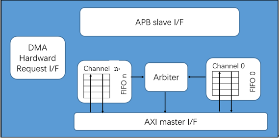
The following figure illustrates the DMAC architecture, comprising the control interface, data transfer interface, independent channel FIFOs, hardware request interfaces, and an internal arbiter.
APB Slave Interface: Used for configuring and accessing the DMAC. The system programs the DMAC via the APB bus, including setting source/destination addresses, configuring channel control registers, and selecting flow controllers. It is also used to read channel interrupts and operating statuses.
AXI Master Interface: The DMAC operates as a master on the AXI bus. It executes data transfers through this interface—reading data from source peripherals and writing it to destination peripherals or memory. This interface fully supports both single and burst transactions.
Hardware Request Interface: Provides a dedicated set of hardware handshake signals for interaction with peripherals. When a peripheral is ready to send or request data, it asserts a hardware request to the DMAC via this interface. The DMAC responds by controlling single or burst transactions according to the protocol.
Channels and FIFOs: The DMAC integrates multiple independent transfer channels to support concurrent multi-tasking. During a transfer, data read from the source is first buffered in the channel’s dedicated FIFO before being written to the destination. This FIFO-based mechanism mitigates transfer bottlenecks caused by clock or processing rate mismatches between the source and destination.
Arbiter: When multiple active DMA channels request data transfers simultaneously, the arbiter grants AXI bus access based on predefined priority scheduling policies. This ensures efficient and orderly utilization of the DMAC master interface resources in high-throughput scenarios.
The DMAC data transfer process is logically divided into three levels:
DMA Transfer
The highest-level operation executed by the DMAC. A complete DMA transfer begins when software enables the DMA channel and ends when the channel is disabled or a transfer complete interrupt is generated.
Depending on application complexity, a DMA transfer can be categorized as:
Single-block Transfer: Contains only a single data block within the entire DMA transfer lifecycle.
Multi-block Transfer: A concatenation of multiple data blocks (e.g., handling non-contiguous memory via linked lists, or periodic refreshes via auto-reload).
Block Transfer
The secondary logical unit constituting a DMA transfer, representing a set of data to be transferred continuously. The DMAC can optionally trigger a block complete interrupt at the end of each block transfer.
Bus Transaction
The fundamental execution unit for data interaction between the DMAC, system buses (e.g., AXI/AHB), and peripheral FIFOs. To maximize bus bandwidth utilization, the DMAC breaks down block transfer requirements into multiple transactions. Transactions are divided into two types:
Burst Transaction:
Once the DMAC wins bus arbitration, it continuously executes a specified number of read/write operations for data items (width determined by CTLx_L.SRC_TR_WIDTH or CTLx_L.DST_TR_WIDTH) without interruption. The burst length is defined by the source or destination burst size parameters (CTLx_L.SRC_MSIZE or CTLx_L.DEST_MSIZE). This mode offers high bus throughput and is suitable for bulk data transfers.
Single Transaction:
Once the DMAC wins bus arbitration, it performs a single read/write operation for one data item (width determined by CTLx_L.SRC_TR_WIDTH or CTLx_L.DST_TR_WIDTH), then releases the bus or waits for the next handshake request. This mode is typically used for handling unaligned tail data that cannot form a complete burst, or for responding to low-speed peripherals with shallow buffers.
Example: If software configures a channel to read 35 data items from a peripheral (Block Size = 35) and sets the burst length to 8. During this block transfer, the underlying bus behavior is:
Execute 4 burst transactions (processing 4 × 8 = 32 data items), then automatically downgrade to execute 3 single transactions (processing the remaining 3 tail data items). These combined transactions complete the entire block transfer.
Note
The block size is configurable only when the DMAC acts as the flow controller.
When a peripheral acts as the flow controller, the block size is unknown, and the transfer depends entirely on transaction requests issued by the peripheral. For details, refer to the Transfer Types and Flow Controller section.
Before enabling a channel for single or multi-block transfers, its fundamental hardware behavior must be defined by programming the channel control registers (CTLx_L and CTLx_H) and configuration registers (CFGx_L and CFGx_H). The following table defines the core parameters determining bus transaction characteristics:
Register / Field
Description
DMAC_CHx_FIFO_DEPTH
Internal FIFO Depth: The internal FIFO depth of channel x, defining the maximum data buffering capacity.
CTLx_L.TT_FC
Transfer Type and Flow Control: Defines the transfer direction (M2M, M2P, P2M, P2P) and the device in charge of flow control (DMAC, source peripheral, or destination peripheral).
CTLx_H.BLOCK_TS
Block Transfer Size: Specifies the total number of data items (Based on source transmission width) contained in a single block transfer.
CTLx_L.SRC_TR_WIDTH
Source Transfer Width: Defines the data bit width for a single source bus access. Must not exceed the system bus width.
CTLx_L.DST_TR_WIDTH
Destination Transfer Width: Defines the data bit width for a single destination bus access. Must not exceed the system bus width.
CTLx_L.SRC_MSIZE
Source Burst Size: The number of data items read from the source per handshake request. If the source address mode is fixed, this value should not exceed 16 to comply with AXI protocol specifications.
CTLx_L.DEST_MSIZE
Destination Burst Size: The number of data items written to the destination per handshake request. If the destination address mode is fixed, this value should not exceed 16.
CTLx_L.SINC/DINC
Source/Destination Address Increment Mode: Indicates whether the address increments or remains fixed after each transfer. If the target is memory and set to “Fixed”, the transfer width must equal the bus width.
CTLx_L.LLP_SRC_EN/LLP_DST_EN
Linked List Control Enable: Enables block chaining via linked lists on the source or destination side, used in conjunction with the LLP_Lx register for complex multi-block transfers.
CFGx_L.RELOAD_SRC/RELOAD_DST
Auto-Reload Enable: In multi-block transfer mode, determines whether to auto-restore the source address register (SARx) or destination address register (DARx) to its initial value at the end of each block transfer.
CFGx_H.SRC_PER/DEST_PER
Peripheral Handshake Interface Assignment: Assigns the channel’s source or destination to a specific hardware handshake interface number when hardware handshaking is selected.
Flow Control Mode: When the destination peripheral acts as the flow controller, this determines when to respond to source transaction requests. 0 responds immediately and enables data pre-fetching. 1 waits for the destination request before responding, disabling data pre-fetching.
The flow controller is a hardware entity that determines the total amount of data to be transferred in a DMA block and triggers termination upon completion. The current chip supports configuring the DMAC or the participating peripheral (source/destination) as the flow controller.
If the transfer data amount is known, the DMAC should be configured as the flow controller. The block size should be programmed into the CTLx_H.BLOCK_TS field.
If the transfer data amount is unknown, the peripheral should be configured as the flow controller. The actual amount of data transferred is entirely determined by the peripheral. For example, when the DMA is used to receive variable-length data from a UART, the CPU does not know in advance how many bytes will be sent, so the UART peripheral should act as the flow controller. When a UART idle timeout or similar event occurs, the peripheral asserts the dma_last signal to the DMAC to terminate the current block transfer.
Memory lacks a handshake interface with the DMAC; therefore, memory can never act as the flow controller. Once a DMA channel is enabled, memory-oriented transfers proceed immediately without waiting for any peripheral transaction requests.
The DMAC supports 4 transfer types and 2 flow controller settings, configured via the CTLx_L.TT_FC field. The following table lists the valid combinations of transfer types and flow controllers:
Transfer Type
Flow Controller
Memory-to-Memory
DMAC
Memory-to-Peripheral
DMAC
Memory-to-Peripheral
Peripheral
Peripheral-to-Memory
DMAC
Peripheral-to-Memory
Peripheral
Peripheral-to-Peripheral
DMAC
Peripheral-to-Peripheral
Source Peripheral
Peripheral-to-Peripheral
Destination Peripheral
The Flow Control Mode (CFGx_H.FCMODE) determines whether the data prefetch mechanism is enabled for the internal FIFO of the DMAC. It dictates the DMAC’s strategy for responding to source requests under specific transfer types:
0: Enable data prefetch (default). Upon receiving a request from the source peripheral, the DMAC immediately reads data to fill the FIFO, without waiting for a request from the destination peripheral.
1: Disable data prefetch. The DMAC only responds to the source peripheral and performs data reads after receiving a request from the destination peripheral. This prevents source data from being read prematurely and stalling in the FIFO.
Warning
CFGx_H.FCMODE is valid only when the transfer type is peripheral-to-peripheral and the destination peripheral is the flow controller (i.e., CTLx_L.TT_FC = 3’b111). For any other configuration (TT_FC != 7), this bit must be kept at 0.
Transactions are the smallest independent actions executed by the DMAC at the hardware level. In peripheral transfers, transactions strictly define the interaction between the DMAC and peripherals. The hardware supports two transaction types:
Single Transaction: Transfers one data item per operation, mapping directly to a single AXI read/write.
Burst Transaction: Configured via software (CTLx_L.SRC_MSIZE / CTLx_L.DEST_MSIZE). The DMAC translates this into a series of AXI incremental bursts or single transactions, ensuring no single AXI burst exceeds the maximum configured size. The burst length must match the FIFO depths of the DMAC and the peripheral.
The total bytes transferred on the bus are determined jointly by the transfer width and burst length.
Parameter binding conditions for specific transfer types or flow controllers:
Peripheral-to-Peripheral
Destination Flow Control: Must set SRC_MSIZE=0 and DST_MSIZE=0, and source/destination widths must be equal (SRC_TR_WIDTH==DST_TR_WIDTH).
Source Flow Control: The destination executes a transfer only when the dma_single signal is asserted.
Memory-to-Peripheral
Destination Flow Control: Must set SRC_MSIZE=DST_MSIZE.
Address alignment and transfer width constraints:
When using hardware handshaking with a peripheral source/destination, the address (SARx/DARx) must be aligned with its corresponding transfer width (CTLx_L.SRC_TR_WIDTH/DST_TR_WIDTH).
When the destination is a peripheral with a fixed address, the total bytes transferred from the source must be a multiple of the destination transfer width (DST_TR_WIDTH bytes).
Note
Memory transfer widths are always aligned to 4 bytes (32-bit) on the physical bus, regardless of the logical transfer width configured by software.
Source and destination address modes can be configured independently:
Increment: The address increments after each transfer to align with the next CTLx_L.SRC_TR_WIDTH / CTLx_L.DST_TR_WIDTH boundary.
Fixed (No Increment): Must be used if the device is reading/writing from/to a peripheral FIFO with a fixed address.
Configuration Guidelines:
- If the source/destination is Memory, set the address mode to Increment.
- If the source/destination is a Peripheral, set the address mode to Fixed.
Triggered when a complete DMA transfer (which may consist of one or more data blocks) finishes successfully.
IntBlock
Block Transfer Complete
Triggered when a single data block transfer completes (i.e., the current block’s data has been successfully written to the destination and acknowledged).
IntPtcErr
Protocol Error
Triggered when the DMAC master port receives an error response on the AXI bus.
IntSecErr
Security Error
Triggered when a CPU in a non-secure context attempts to access a register belonging to a TrustZone secure channel (only applicable when secure mode is enabled).
Taking the transfer-complete interrupt as an example, the hardware logic for interrupt generation is as follows:
Masking and Generation Mechanism of the Transfer-Complete Interrupt
The interrupt handling flow consists of the following stages:
Raw Status Latch: When an interrupt event occurs, the hardware first latches it into the corresponding raw status register (RAW_*). This flag remains set until explicitly cleared by software.
Interrupt Masking: The hardware performs a bitwise AND operation on the raw status (RAW_*), the corresponding mask register (MASK_*), and the channel’s global interrupt enable bit (CTLx_L.INT_EN).
Status Generation and Aggregation: The final effective result of the masking operation is stored in the status register (STAT_*). Additionally, the combined status register (STAT_INT) performs a bitwise OR across all individual status registers to aggregate the currently unmasked interrupt status of each channel.
Interrupt Clear Mechanism: Software writes 1 to the corresponding bit of the clear register (CLR_*) to simultaneously clear the flags in both the raw status (RAW_*) and the masked status (STAT_*) within the same clock cycle, and to deassert the physical interrupt request signal.
Note
If an interrupt event occurs but is masked by the MASK register or INT_EN, the external status flag and the physical interrupt signal are suppressed. However, the corresponding bit in the raw status register (RAW_*) is still set, recording the occurrence of the event.
If the source or destination address is located in a cacheable memory region, software must explicitly perform a D-Cache Clean operation before initiating the DMA transfer, to flush dirty data from the cache back to main memory.
Before the CPU reads the destination data after a DMA transfer completes, software must perform a D-Cache Invalidate operation to force the CPU to reload the latest data from main memory, preventing stale cache lines from causing data incoherency.
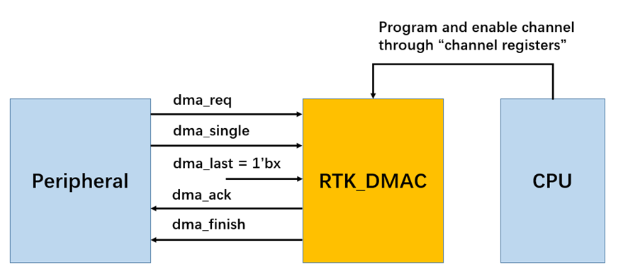
The handshake interface is utilized at the Transaction level to control the flow of Single or Burst Transactions. The operation of the handshake interface varies depending on whether the peripheral or the DMAC serves as the flow controller.
Peripherals use the handshake interface to indicate to the DMAC that they are ready to transfer or accept data over the bus.
Peripherals can request DMA transfers from the DMAC using the hardware handshake interface.
Note
In the remainder of this document, references to the source and destination hardware handshake interfaces assume active-high polarity (refer to the CFGx_L.SRC_HS_POL or CFGx_L.DST_HS_POL bits in the channel configuration register). When using active-low handshake interfaces, the active levels and edges are opposite to those of the active-high interfaces.
The type of handshake interface depends on whether the peripheral is the flow controller.
Tip
Source and destination peripherals can independently select the handshake interface type. There are two interface types:
Hardware Handshake: Supported by default. For more information, refer to the CFGx_L.HS_SEL_SRC and CFGx_L.HS_SEL_DST parameters in the CFGx register.
Software Handshake: Not supported.
All hardware handshake interfaces and their corresponding peripherals are fixed during chip design and cannot be altered by the user. The hardware handshake interfaces supported by the current chip and their corresponding IPs are listed in the following table:
When the DMAC acts as the flow controller, it attempts to transfer data efficiently using as little bus bandwidth as possible. Typically, the DMAC tries to use Burst Transactions and fill or empty the channel FIFO in a burst, provided the software has not restricted the burst length.
Signals
Figure DMAC as Flow Controller illustrates the hardware handshake interface between the peripheral and the DMAC when the DMAC is the flow controller.
The following table describes the hardware handshake signals when the DMAC acts as the flow controller. The signal polarity can be programmed using the CFGx_L.SRC_HS_POL and CFGx_L.DST_HS_POL fields.
Signal
Direction
Description
dma_req
Input
Burst transaction request from the peripheral.
The DMAC always interprets dma_req as a burst request, regardless of the level of dma_single.
Type: Level-sensitive.
Handshake: Once the peripheral asserts dma_req, the signal must remain asserted until the DMAC asserts dma_ack.
Completion: The peripheral should deassert dma_req after receiving dma_ack from the DMAC (indicating the completion of the burst). The DMAC will deassert dma_ack once the peripheral deasserts dma_req.
dma_single
Input
Single transaction status.
Asserted by the corresponding peripheral when the destination peripheral can accept at least one data item or the source peripheral can send at least one data item; otherwise, it is deasserted.
Handshake: Once asserted, dma_single must remain asserted until dma_ack is asserted. The peripheral must then deassert dma_single.
Validity: This signal is sampled only in the single transaction region of the block transfer. Outside this region, it is ignored (all transfers are treated as bursts).
dma_last
Input
Ignored. Because the peripheral is not the flow controller, the DMAC does not sample this signal.
dma_ack
Output
DMAC acknowledge signal. Asserted after the data phase of the final AXI transfer of the current transaction (single or burst).
Deassertion Trigger:
Single transaction: Remains asserted until the peripheral deasserts dma_single.
Burst transaction: Remains asserted until the peripheral deasserts dma_req.
Deassertion Timing:
If using a synchronous handshake interface, dma_ack is deasserted after 1 dmac_clk cycle.
If using an asynchronous handshake interface, dma_ack is deasserted after 6 + SYNC dmac_clk cycles, where SYNC is the number of synchronization stages.
dma_finish
Output
Block completion signal. The DMAC asserts this signal to indicate the completion of the entire block transfer.
Timing: Generally follows the same timing as dma_ack.
Handshake Loop: Forms a closed loop with dma_req or dma_single.
Exception: When the destination peripheral is the flow controller, the timing definition of the interaction between dma_finish and the source peripheral interface differs from the above.
Note
For dma_ack and dma_finish, when the channel enable register is enabled and HS_POL is configured as active-low, these signals may still exhibit a brief “active” level before the block transfer truly begins, as the module has not yet fully transitioned into the working state.
Timing Diagram
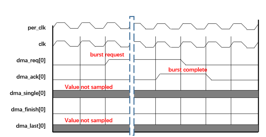
Figure Burst Transaction Example shows a timing diagram for a burst transaction where the peripheral clock per_clk is equal to dmac_clk. In this example, the peripheral is outside the single transaction region, so the DMAC does not sample dma_single.
If the peripheral is an AXI peripheral, the per_clk signal equals dmac_clk; if it is an APB peripheral, it equals pclk. The burst transaction request signal dma_req and the single status signal dma_single are generated by the peripheral located in the per_clk domain and are sampled by clk within the DMAC. The acknowledge signal dma_ack is generated by RTK_DMAC located in the dmac_clk domain and is sampled by per_clk in the peripheral. The handshake mechanism between the DMAC and peripherals supports quasi-synchronous clocks: that is, dmac_clk and per_clk must be phase-aligned, and when using a synchronous handshake interface, the dmac_clk frequency must be a multiple of the per_clk frequency.
If the destination peripheral is an APB peripheral and buffered writes are performed via an APB bridge, care must be taken to prevent the destination peripheral FIFO from overflowing.
Cause of Overflow: The write completes on the AXI bus but has not yet completed on the APB bus (the write may still be buffered in the APB bridge).
Overflow Scenario:
As soon as the write transaction completes on the AXI interface, the DMAC asserts dma_ack.
The APB peripheral deasserts its request signal after sampling the assertion of the acknowledge signal.
Because the data is still buffered in the bridge and has not reached the FIFO, the peripheral perceives that there is still space. Consequently, it reasserts the request signal one APB clock cycle later.
The peripheral may only have space for one data item, which will eventually be consumed by the first (pending) buffered write. The initiation of the second transaction may overflow the FIFO.
Solution: To avoid this situation, one of the following two strategies must be adopted during system design:
Disable buffered writes to ensure synchronous bus write operations.
If buffered writes are used, ensure that the dma_ack signal from the DMAC is forcibly delayed until the data is actually written to the APB peripheral. The specific method involves routing the dma_ack signal to the APB bridge.
Note
If write operations are not buffered, the initiation of the second transaction will not occur, as the destination peripheral will correctly perceive that its FIFO is full.
When a peripheral is configured as the flow controller, the peripheral controls the total length of the block. It is responsible for explicitly signaling the DMAC when the block transfer is complete.
Signaling Completion: The peripheral completes the end-of-block indication by indicating to the DMAC that the current transaction (whether burst or single) is the last transaction in the block.
Transaction Type Selection: The peripheral directly indicates to the DMAC the type of transaction to execute. When the block size is not an integer multiple of CTLx_L.SRC_MSIZE/CTLx_L.DEST_MSIZE, the peripheral must use single transactions to complete the block transfer.
Note
Because the peripheral can initiate single transactions and terminate blocks, the concept of the Single Transaction Region does not apply to this mode.
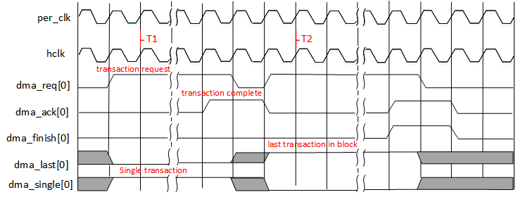
Signals
Figure Peripheral as Flow Controller shows the hardware handshake interface between the destination or source peripheral and the DMAC when the peripheral is the flow controller.
The following table describes the operation of the hardware handshake interface signals when the peripheral is the flow controller:
Signal
Direction
Description
dma_req
Input
Transaction request from the peripheral. An active level on dma_req initiates the request, while the specific transaction type (single or burst) is determined by the dma_single signal.
Handshake Protocol: Once dma_req is asserted, it must remain asserted until dma_ack is asserted. The peripheral must deassert dma_req when it detects the assertion of dma_ack.
dma_single
Input
Determines the transaction type (single or burst), sampled in the same clock cycle as the rising edge of the dma_req signal.
Burst transaction: When dma_single is deasserted.
Single transaction: When dma_single is asserted.
dma_single must remain stable while dma_req is active and cannot toggle arbitrarily.
dma_last
Input
Indicates the last transaction in the block. When the peripheral is the flow controller, dma_last is asserted in the same cycle as dma_req.
If dma_single is high: The last transaction is a single transaction.
If dma_single is low: The last transaction is a burst transaction.
dma_last must remain stable while dma_req is active.
dma_ack
Output
Acknowledge signal from the DMAC. Asserted after the completion of the data phase of the last AXI transfer of the current transaction (single or burst). This signal forms a handshake loop with dma_req and remains asserted until the peripheral deasserts dma_req.
If using a synchronous handshake interface: Deasserted within 1 cycle after detecting the deassertion of dma_req.
If using an asynchronous handshake interface: Deasserted after a delay of (6 + SYNC) cycles following the detection of the deassertion of dma_req.
dma_finish
Output
Signals the completion of the block transfer. The DMAC asserts dma_finish to signal block transfer completion, using the same timing as dma_ack, and forms a handshake loop with dma_req.
Note
For dma_ack and dma_finish, when the channel enable register is enabled and HS_POL is configured as active-low, these signals may still exhibit a brief “active” level before the block transfer truly begins, as the module has not yet fully transitioned into the working state.
Timing Diagrams
Burst Transaction Followed by Single Transaction
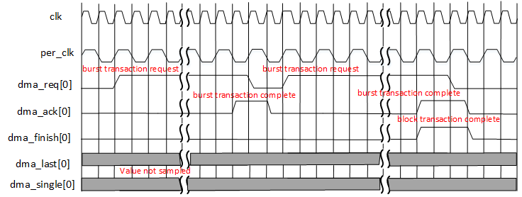
Figure Timing Diagram 1 illustrates the scenario of a burst transaction followed by a single transaction using a synchronous handshake interface, where the single transaction is the last in the block.
At clock edge T1, the DMAC samples dma_req as asserted, dma_single as deasserted, and dma_last as deasserted. This indicates that the peripheral is requesting a burst transfer from the DMAC and informing the DMAC that there is subsequent data.
At clock edge T2, the DMAC samples dma_req, dma_single, and dma_last as all asserted. This indicates that the peripheral is requesting a single transfer from the DMAC and informing the DMAC that data transfer is complete. Both dma_last and dma_single only need to be active in the same clock cycle that dma_req is asserted.
Similarly, Figure Timing Diagram 2 illustrates the scenario of a single transaction followed by a burst transaction using a synchronous handshake interface, where the burst transaction is the last in the block.
Warning
It is illegal to configure the source or destination as the flow controller while disabling the corresponding hardware handshake.
If the transfer type is peripheral-to-peripheral and the destination is the flow controller:
Burst length restriction: The burst lengths for the source and destination (CTLx_L.SRC_MSIZE and CTLx_L.DEST_MSIZE) must be 0.
Bus width alignment restriction: The transfer widths for the source and destination (CTLx_L.SRC_TR_WIDTH and CTLx_L.DST_TR_WIDTH) must be equal.
Known exception: When CTLx_L.TT_FC is set to 3’b111 and CFGx_H.FCMODE is set to 1, dma_finish for the source might not be asserted even after the entire transfer finishes.
Peripheral hardware initiates different types of DMA transfer requests by continuously monitoring its own FIFO data depth and triggering them when predefined thresholds are met:
Source Peripheral Request: When the amount of data in the source peripheral’s internal FIFO reaches or exceeds the configured trigger threshold, it asserts the dma_req signal (producing an active edge), requesting the DMAC to read and transfer the data.
Destination Peripheral Request: When the amount of data in the destination peripheral’s internal FIFO falls below the configured trigger threshold, it asserts the dma_req signal, requesting the DMAC to write and fill the data.
To maximize bus utilization, the FIFO trigger threshold configurations should strictly align with the burst transaction size of the DMAC channel:
For best bus efficiency, the amount of data reserved by the peripheral (or available space) should exactly satisfy the needs of one DMAC burst transaction.
In peripheral-to-memory transfer scenarios, if the residual data in the peripheral FIFO is insufficient to reach the DMA request threshold (and the bus is idle with no new incoming data), the peripheral typically relies on its built-in hardware timeout or force-flush mechanism to actively trigger a DMA transfer of the residual data or to report an interrupt request to the processor.
In peripheral-to-memory transfer scenarios, if the residual data in the peripheral FIFO is insufficient to reach the threshold that triggers a DMA request (and the bus is idle with no new incoming data), it typically relies on the peripheral hardware’s built-in timeout mechanism or forced Flush mechanism to proactively trigger a DMA transfer for the residual data or to report an interrupt request to the processor.
During a DMA block transfer, single transaction transfers are used in certain situations, depending on the flow controller role:
When the DMAC is the flow controller, the total transfer data amount is known. If any of the following conditions are met, the DMAC will automatically control the source or destination to execute single transaction transfers:
The burst length for the source or destination (CTLx_L.SRC_MSIZE or CTLx_L.DEST_MSIZE) is configured to 0 by software.
The block transfer is nearing completion, and the remaining amount of data to be transferred is insufficient to form a complete burst read/write transaction (the underlying hardware automatically downgrades to handle the tail data using single transactions).
When the peripheral is the flow controller, the total transfer data amount is unknown. The peripheral must explicitly request single transfers via hardware handshake signals (typically used for handling unaligned tail data). If either of the following conditions is met, the corresponding endpoint will execute a single transaction:
If the source peripheral is the flow controller: When the asserted dma_single and dma_req signals are active in the same clock cycle.
If the destination peripheral is the flow controller: When the asserted dma_single and dma_req signals are active in the same clock cycle.
Each DMA channel contains two independent, parallel-running state machines:
Source state machine
Destination state machine
These state machines issue bus occupancy requests to the internal arbiter based on transfer demand. A successful data transfer must strictly satisfy the following three conditions in order:
Internal FIFO ready: Only when the DMAC channel’s internal FIFO reaches the ready state (sufficient space to write on the source side, or sufficient data available on the destination side) can the subsequent bus request proceed.
Gain AXI master interface control (first-level arbitration): After the source or destination state machine issues a request, it must be selected by the channel’s internal arbiter to obtain control of the DMA AXI master interface.
Gain external AXI bus control (second-level arbitration): When the AXI master interface initiates a read/write transaction on behalf of the state machine, it must win arbitration from the system bus matrix to obtain physical control of the external AXI bus.
Whether an AXI transfer can initiate depends directly on the readiness state of the DMAC’s internal channel FIFO:
For Single Transactions:
Source Read Ready: The channel FIFO must have sufficient remaining space to accommodate at least one data item of width CTLx_L.SRC_TR_WIDTH.
Destination Write Ready: The channel FIFO must have buffered enough data to satisfy at least one data item of width CTLx_L.DST_TR_WIDTH.
For Burst Transactions:
Source Read Ready: The channel FIFO must have sufficient remaining space to accommodate the data for the entire burst length (CTLx_L.SRC_MSIZE transfers × CTLx_L.SRC_TR_WIDTH).
Destination Write Ready: The channel FIFO must have buffered the data for the entire burst length (CTLx_L.DEST_MSIZE transfers × CTLx_L.DST_TR_WIDTH).
Under certain special configurations, the actual read/write burst length (ARLEN/AWLEN) on the AXI bus is forced by hardware to not exceed FIFO_DEPTH/2. The conditions that trigger this restriction are:
The source address (SARx) or destination address (DARx) is not aligned to the DMAC transfer width.
Scatter/Gather is enabled and the transfer type is configured as address-increment (INCR). For detailed mechanism, refer to the Scatter/Gather section.
The current DMAC hardware configuration does not support burst lengths greater than the FIFO depth, and the channel FIFO depth does not exceed 256 under the current system bus width.
Peripheral Transfers: The source/destination state machine must simultaneously satisfy both “FIFO ready” and “received a single/burst handshake request from the peripheral” before formally issuing a bus read/write request to the AXI master interface.
Memory Transfers: Because memory has no hardware handshake signals, the state machine issues a request to the AXI master interface as soon as the internal FIFO is ready. If the target memory (or bus slave) is not yet ready to receive or provide data, wait states will be inserted on the AXI bus.
Caution
When the destination peripheral acts as the flow controller and software has set CFGx_H.FCMODE=1 (i.e., data prefetch is disabled), the source state machine will not generate an AXI read request even if the source FIFO space is ready and the source peripheral has issued a request, unless the destination peripheral explicitly issues a handshake signal requesting new data.
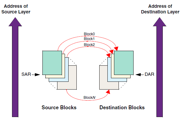
The DMAC supports both single-block and multi-block transfer modes. During a multi-block transfer, when the current block (Block N) completes, the hardware automatically reprograms the channel registers to seamlessly continue with the next block (Block N+1).
The DMAC provides three fundamental register update strategies. The source and destination can independently choose which mechanism to use:
Block chaining using linked lists (Linked List): Via the LLP_Lx register, the hardware actively fetches the next LLI from system memory and uses its contents to overwrite the channel registers to start the next block.
Auto-reload of channel registers (Auto-reload): At the end of each block transfer, the hardware automatically restores the specified channel registers to the initial configuration values from when the channel was first enabled.
Contiguous block addresses (Contiguous): The starting address of the current block is automatically set by the hardware to immediately follow the ending address of the previous block.
The following table summarizes the register update behavior for each mode:
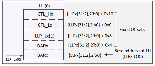
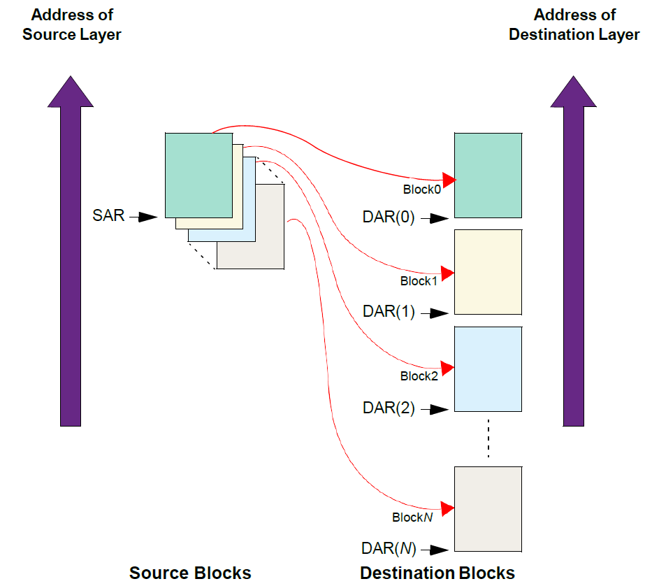
Block chaining using linked lists is commonly used for transferring non-contiguous data blocks, as illustrated in Source and Destination Both Using Linked Lists. In this mode, the driver software organizes a linked list in system memory, consisting of a series of linked list items (LLIs). Before each data block transfer begins, the DMAC actively fetches the pre-built LLI from system memory to reprogram the channel registers, enabling multi-block transfers.
Each LLI consists of the following four core register fields, which together with the channel configuration register CFGx_L/H determine the transfer attributes of the data block:
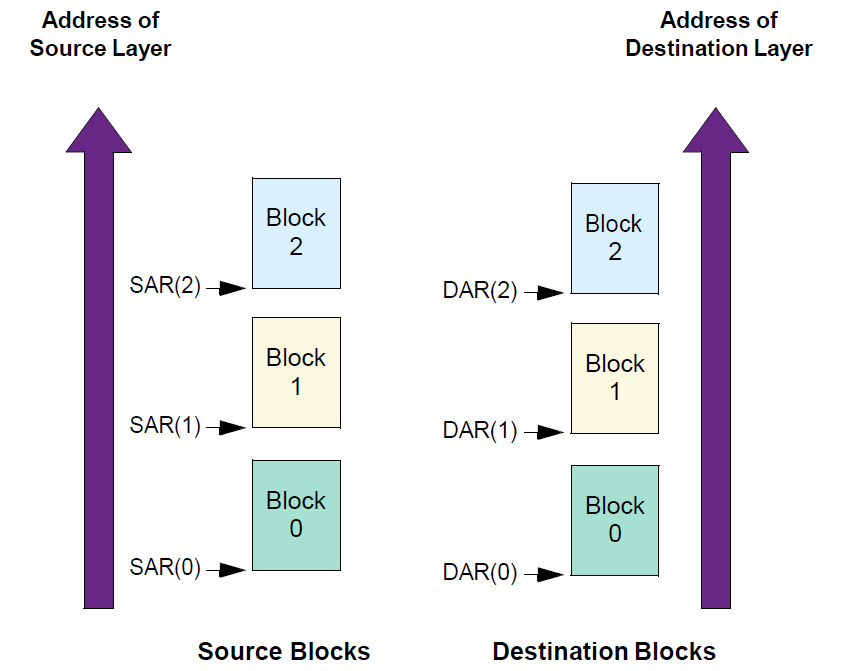
SARx: Source address register
DARx: Destination address register
CTLx_L/H: Control register
LLP_Lx: Linked list pointer register
The following figure shows the structure of an LLI:
The following figure illustrates the mapping from LLI fields in memory to channel registers:
The physical address of LLI.CTLx equals the LLI base address (stored in LLP_Lx) plus a fixed hardware offset. For example, the address of LLI.CTLx is LLP_Lx.LOC+0x0C.
LLP_Lx is always updated via the linked-list mechanism. Before the transfer starts, the head address of the linked list must be written to the channel register LLP_Lx. The LLP_Lx field in each LLI always points to the next LLI.
Linear linked list: If the last LLI’s LLP_Lx is a null address and CTLx_L.LLP_SRC_EN or CTLx_L.LLP_DST_EN is cleared, the DMAC identifies the current block as the last block of the multi-block transfer and stops after completion.
Circular linked list: If the last LLI’s LLP_Lx points back to the head address and CTLx_L.LLP_SRC_EN or CTLx_L.LLP_DST_EN is set, the DMAC identifies the current block as an intermediate block and continues from the head address after completion.
Warning
Memory access to LLI fields is strictly 32-bit aligned, and this behavior cannot be configured.
Under the auto-reload mechanism, by enabling CFGx_L.RELOAD_SRC or CFGx_L.RELOAD_DST, the DMAC automatically restores some or all fields of SARx, DARx, and CTLx to their initial values at the end of each block transfer, then starts the next block transfer.
When auto-reload is enabled and block-complete interrupts are enabled, the user must clear the block-complete interrupt after each block transfer completes. Otherwise, the interrupt line will remain asserted and cannot be re-triggered.
In Contiguous mode, the starting address of each block seamlessly follows the ending address of the previous block. This mode is typically combined with Auto-reload or Linked List, and is well suited for asymmetric transfer scenarios where one end increments continuously while the other is fixed or discrete. For example:
Large contiguous memory to fixed-address block: Configure the source as Contiguous to read continuously from a large data buffer; configure the destination as Auto-reload to always write to a fixed address block.
Discrete memory to large contiguous memory: Configure the source as Linked List to read from discrete address blocks; configure the destination as Contiguous to concatenate the received blocks into a large contiguous memory region.
Whether the source or destination uses Contiguous mode is determined jointly by the linked-list enable bit in CTLx_L and the auto-reload enable bit in CFGx_L.
To configure one end (source or destination) as Contiguous, both its linked-list update and auto-reload must be disabled simultaneously:
You cannot configure both SARx and DARx update methods as Contiguous simultaneously. If both ends must be contiguous between blocks, use one of the following approaches:
Increase single-block transfer size: Configure CTLx_H.BLOCK_TS to complete all data within a single block where possible.
Use Linked List mode: If CTLx_H.BLOCK_TS has reached its maximum, use Linked List mode and explicitly set LLI.SARx and LLI.DARx in the next LLI to equal the corresponding end addresses of the previous block.
Linked list mode: DMA transfer executes continuously between blocks with no stall at block boundaries. For example, at the end of block N, the DMAC automatically continues processing block N+1.
Auto-reload mode:
If block-complete interrupts are enabled and not masked, the DMA transfer automatically stalls after the interrupt is triggered. The DMAC will not start the next block until hardware detects a write to the ClearBlock[n] register (clearing the block-complete interrupt for that channel).
If interrupts are disabled (CTLx_L.INT_EN=0) or block interrupts are masked (MaskBlock[n]=0), the DMA transfer does not stall between blocks and proceeds directly to the next block.
Warning
When using auto-reload in a multi-block transfer, software must clear the auto-reload control bits (CFGx_L.RELOAD_SRC / CFGx_L.RELOAD_DST) in the ISR of the penultimate block transfer, to prevent unintended reloading and transfer.
The update mechanism used by the source and destination is determined jointly by whether the linked-list pointer is null (LLP_Lx.LOC=0), the linked-list enable bit (CTLx_L.LLP_EN), and the auto-reload enable bit (CFGx_L.RELOAD). The DMAC supports 10 combination modes; Table Transfer Types and Configuration Bits lists the typical configurations.
Single-block or last block of multi-block transfer (SARx/DARx reprogrammed by software)
0
0
0
0
0
No
2
Auto-reload: SAR auto-reload, DAR contiguous
0
0
0
0
1
No
3
Auto-reload: SAR contiguous, DAR auto-reload
0
0
1
0
0
No
4
Auto-reload: both SAR and DAR auto-reload
0
0
1
0
1
No
5
Single-block or last block of multi-block transfer (SARx/DARx reprogrammed by software)
1
0
0
0
0
Yes
6
Linked list: SAR contiguous, DAR linked list
1
0
0
1
0
Yes
7
Linked list: SAR auto-reload, DAR linked list
1
0
1
1
0
Yes
8
Linked list: SAR linked list, DAR contiguous
1
1
0
0
0
Yes
9
Linked list: SAR linked list, DAR auto-reload
1
1
0
0
1
Yes
10
Linked list: both SAR and DAR linked list
1
1
0
1
0
Yes
Row 1 or row 5 of Table Transfer Types and Configuration Bits represents the register state when transferring the last block (single block or multi-block). The termination path depends on which row the transfer started from:
Transfers starting from rows 2, 3, 4: must end with the row 1 register state, which disables status fetch and write-back for the last block.
Transfers starting from rows 6 to 10: must end with the row 5 register state, which enables status fetch and write-back for the last block.
Note
The LLP_Lx.LOC bit is sampled only once when the channel is enabled and transfer starts. It determines whether write-back is enabled for the entire transfer; modifying this bit in subsequent blocks of the same multi-block transfer has no hardware effect.
Based on the above rules, termination for each mode is as follows:
Terminating auto-reload: When LLP_Lx.LOC=0 and either end has auto-reload enabled, the multi-block DMA transfer runs continuously. Software must simultaneously clear CFGx_L.RELOAD_SRC and CFGx_L.RELOAD_DST in the ISR for the penultimate block, causing the next block’s register state to match row 1 and terminating transfer when that block completes.
Terminating linked list transfers: Software must set the appropriate LLI.CTLx_L for the last block’s LLI in system memory, ensuring both LLI.CTLx_L.LLP_SRC_EN and LLI.CTLx_L.LLP_DST_EN are 0, to match the row 5 state and terminate transfer when that block completes.
Valid state transitions: The only allowed transition in the configuration table is from any row to row 1 or row 5 (to terminate the DMA transfer). Direct transitions between any other two rows are not permitted. For example, if block N is configured as row 10, block N+1 may only remain at row 10 or transition to row 5; transitioning directly to row 8 or any other row is an illegal configuration.
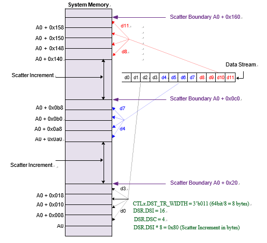
Scatter/Gather operates within the same data block, moving data non-contiguously by jumping according to a fixed pattern (Stride SGI/DSI and Count SGC/DSC). This is frequently used for 2D image cropping, matrix transposition, or separating interleaved audio channels.
Scatter relates to destination transfers. When a scatter boundary is reached, the destination address increments by a programmed amount—the scatter increment.
Figure Example of Destination Scatter Transfer displays an example of a destination scatter transfer. Upon hitting the scatter boundary, the destination address increments by the value stored in the destination scatter increment (DSRx_L.DSI) field, multiplied by the number of bytes per single AXI transfer to the destination (decoded value of CTLx_L.DST_TR_WIDTH) / 8. Users can configure the number of transfers between consecutive scatter boundaries by programming the DSC (Destination Scatter Count) field in the DSRx_L register.
Scatter is enabled by writing a 1 to the CTLx_L.DST_SCATTER_EN field. The CTLx_L.DINC field determines whether the address increments or remains fixed. If CTLx_L.DINC dictates fixed address control for the entire DMA transfer, the CTLx_L.DST_SCATTER_EN field is ignored, and the scatter feature is automatically disabled.
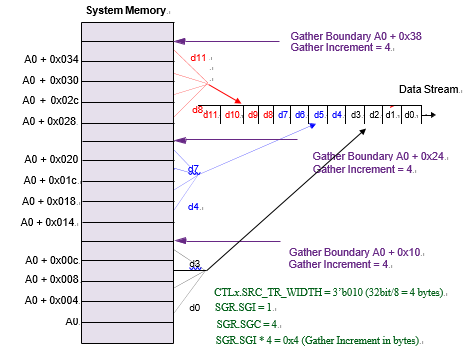
Gather relates to source transfers. When a gather boundary is reached, the source address increments by a programmed amount.
The number of source transfers between consecutive gather boundaries is programmed into the Source Gather Count (SGRx_L.SGC) field.
Upon hitting a gather boundary, the source address increments by the value stored in the source gather increment (SGRx_L.SGI) field, multiplied by the number of bytes per single AXI transfer from the source (decoded value of CTLx_L.SRC_TR_WIDTH) / 8.
Gather is enabled by writing a 1 to the CTLx_L.SRC_GATHER_EN field. The CTLx_L.SINC field determines whether the address increments or remains fixed when reaching the gather boundary. If CTLx_L.SINC dictates fixed address control for the entire DMA transfer, the CTLx_L.SRC_GATHER_EN field is ignored, and the gather feature is automatically disabled.
Figure Example of Source Gather Transfer displays an example of a source gather transfer. The number of source transfers between consecutive gather boundaries is programmed into the SGRx_L.SGC field. Upon hitting the gather boundary, the source address increments or decrements by the value in SGRx_L.SGI multiplied by the byte width of a single AXI transfer from the source.
Where TWB is the Transfer Width in Bytes (decoded value of CTLx_L.SRC_TR_WIDTH/8 = src_single_size_bytes).
Note
For multi-block transfers, the counters tracking the number of transfers required to reach a gather/scatter boundary are reinitialized at the beginning of each block transfer to the Source Gather Count (SGRx_L.SGC) and Destination Scatter Count (DSRx_L.DSC).
The DMAC is fully compatible with the system’s secure isolation architecture (such as ARM TrustZone). It supports configuring specific channels as secure channels, allowing the DMAC to execute data movements across protected memory or peripheral regions on behalf of the “Secure World”.
Under standard isolation mechanisms, if a channel operating in normal (non-secure) mode attempts to read a protected secure region, the system hardware firewall will typically intercept the operation and return a bus error or invalid data; if it attempts to write, the write transaction is silently discarded.
Only when secure privilege is explicitly allocated to a channel in the configuration register will the DMAC initiate accesses with secure attributes, thereby legitimately passing the system’s secure check nodes.
The standard workflow for a secure DMA transfer is as follows:
Note
The following configuration sequence must be executed while the processor is in Secure Privilege Mode. Non-secure CPU accesses will be denied write operations to DMAC secure configuration registers.
Allocate Secure Privilege: In the configuration register for a specific channel, set the Secure Access Bit to 0 (please refer to specific register definitions for exact active levels).
Initiate Transfer: Enable the DMAC transfer channel normally.
Wait for Completion: Wait for the DMAC transfer to complete naturally, or wait for the corresponding interrupt trigger. Upon completion, the DMAC automatically clears the channel’s enable bit.
Revoke Privilege: Adhering to the principle of least privilege, once the channel no longer needs to move secure data, software should immediately revert the secure access bit to a non-secure state to prevent the channel from being exploited by malicious code.
Under normal operation, software starts a channel by writing 1 to the channel enable register (CHENREG_L/H.CH_EN). Upon completion of the transfer, hardware automatically clears this bit to disable the channel. If software needs to intervene before natural completion, the DMAC provides two mechanisms: Safe Suspend and Abnormal Termination.
To preemptively disable a channel without losing data or inducing bus deadlocks, it is highly recommended to use a safe procedure coordinating the CFGx_L.CH_SUSP and CFGx_L.INACTIVE flags:
Trigger Suspend: Write 1 to CFGx_L.CH_SUSP. The DMAC will halt fetching new data from the source, and the channel FIFO will stop accepting new inputs.
Wait for Drain: Poll the CFGx_L.INACTIVE bit until it reads 1, indicating that the channel FIFO is empty and all current bus transactions have concluded.
Note
If using a hardware handshake interface, the peripheral must keep the handshake signals (dma_req / dma_single) asserted until INACTIVE is set, to ensure the DMAC completes the current suspend handshake maneuver.
Disable Channel: Once INACTIVE is set, software writes 0 to CHENREG_L/H.CH_EN to safely disable the channel. The hardware automatically clears CH_SUSP. (If INACTIVE is not set, the write to 0 is ignored by hardware.)
Clean up Status: After disabling the channel, software must manually clear all interrupt status bits for that channel.
Note
After executing a suspend-and-cancel, all channel registers retain their original values except for CH_SUSP. Software can restart the identical transfer simply by re-setting CH_EN.
If software writes 0 back into CFGx_L.CH_SUSP before disabling the channel (clearing CH_EN), the channel will exit the suspended state. The DMA transfer will seamlessly resume from the exact point of suspension without any data loss.
When INACTIVE is asserted, residual data may still remain in the FIFO. If the channel is disabled at this point, how the residual data is handled and the read-back accuracy of the address registers depend on the transfer flow direction:
Memory-to-Memory / Peripheral-to-Memory: No data loss. The DMAC ensures the remaining data in the FIFO is written to the destination memory. After suspend and disable, the read-back values of CURR_SARx, CURR_DARx, and CTLx_H are precise.
Memory-to-Peripheral / Peripheral-to-Peripheral: Residual data in the FIFO may be lost. If the destination peripheral cannot accept more data (e.g., handshake signal not asserted) during suspend, the DMAC is unable to write out the remainder and discards it. After suspend and disable, the read-back value of CTLx_H is precise, but CURR_SARx and CURR_DARx (for fixed-address mode) are imprecise.
Software can forcibly terminate a transfer by clearing the enable bits, but must strictly follow the polling requirement and accept the resulting side effects.
Warning
If the hardware configuration does not have the Suspend Feature enabled, writing 0 to CH_EN while the channel is active is strictly forbidden.
Operations include clearing CHENREG_L/H.CH_EN for a single channel, or clearing the global enable bit in the DMAC configuration register. After issuing the disable request, software must poll and read back 0 to confirm the channel has been completely shut down, because the DMAC must finish processing any AXI responses already in progress on the bus.
Side effects of abnormal termination:
Permanent Data Truncation: Data in the FIFO at the time of forced disable is discarded. For read-sensitive source peripherals (e.g., source FIFOs), this results in substantial data loss.
Handshake Interruption: A forcibly disabled channel may fail to send a hardware acknowledge signal to active transactions.
Burst Limitation: If the channel is configured for defined-length bursts (DMAC_INCR_BURSTS=0), forcibly disabling the channel via software before transfer completion is not supported.
Three registers (LLP_Lx, CTL_L/Hx, and CFG_L/Hx) must be programmed to determine whether to execute a single-block or multi-block transfer, and which type of multi-block transfer to utilize. Various transfer types are illustrated in Transfer Types and Configuration Bits.
The “Update Method” columns dictate from where the values for the SARx, CURR_SARx, DARx, CURR_DARx, CTL_L/Hx, and LLP_Lx registers are acquired for the subsequent block when multi-block DMAC transfers are enabled.
Note
Any combinations of LLP_Lx.LOC=0, CTLx_L.LLP_SRC_EN, CFGx_L.RELOAD_SRC, CTLx_L.LLP_DST_EN, and CFGx_L.RELOAD_DST other than those listed in Transfer Types and Configuration Bits are illegal and will result in undefined or erroneous system behavior.
Row 5 in Transfer Types and Configuration Bits is also a single-block transfer, but it features write-back functionality for control and status information enabled at the end of the transfer.
Read the Channel Enable register to select a free (disabled) channel.
Clear any pending interrupts on this channel from previous DMA transfers by writing data to the interrupt clear registers (CLEARTFR_L/H, CLEARBLOCK_L/H, and CLEARERR_L/H). Reading the raw interrupt status and interrupt status registers can confirm that all interrupts have been successfully cleared.
Program the following channel registers:
Write the starting source address to the SARx register of Channel x.
Write the starting destination address to the DARx register of Channel x.
Program CTL_L/Hx and CFG_L/Hx according to the Row 1 configuration shown in Transfer Types and Configuration Bits. Program the LLP_Lx register to 0.
Write the control information for the DMA transfer into the CTL_L/Hx register of Channel x. For instance:
Set the transfer type (whether source and destination are memory or peripherals) and the flow control device by programming the TT_FC field in CTLx_L.
Set transfer characteristics:
Set the source transfer width in the SRC_TR_WIDTH field.
Set the destination transfer width in the DST_TR_WIDTH field.
Configure the source address as incrementing/decrementing or fixed in the SINC field.
Configure the destination address as incrementing/decrementing or fixed in the DINC field.
Write channel configuration information into the CFG_L/Hx register of Channel x:
Specify the hardware handshake interface type for the source and destination peripherals (not required for memory transfers). This involves programming the HS_SEL_SRC / HS_SEL_DST bits. Writing 0 activates the hardware handshake interface; writing 1 activates the software handshake interface.
If hardware handshake interfaces are activated, assign them to the appropriate peripherals by programming the SRC_PER and DEST_PER bits.
If Gather is enabled (DMAC_CHx_SRC_GAT_EN=True and CTLx_L.SRC_GATHER_EN is enabled), program the SGR_L/Hx register.
If Scatter is enabled (DMAC_CHx_DST_SCA_EN=True and CTLx_L.DST_SCATTER_EN is enabled), program the DSR_L/Hx register.
After finalizing programming for the selected channel, enable it by writing 1 to CHENREG_L/H.CH_EN. Ensure that bit 0 of the DMACFGREG_L/H register is also enabled.
The source and destination peripherals request single and burst DMA transactions to transfer the data block. The DMAC issues an acknowledgment upon the completion of each transaction and executes the block transfer.
Once the transfer is complete, the hardware asserts the corresponding interrupt and disables the channel. Software can service the “Block Complete” or “Transfer Complete” interrupts, or poll the raw interrupt status register (RAWTFR[n]) until it is asserted. If polling is utilized, software must ensure the interrupt is cleared by writing to CLEARTFR[n] before re-enabling the channel.
Read the Channel Enable register to select a free (disabled) channel.
Set up the chain of Linked List Items (LLI) in memory. Write the control information into the LLI.CTL_L/Hx register location of each LLI block descriptor. For example:
Set the transfer type and flow control device in CTLx_L.TT_FC.
Set transfer characteristics (SRC_TR_WIDTH, DST_TR_WIDTH, SINC, DINC).
Write channel configuration details to the CFG_L/Hx register:
Specify the handshake interface type (HS_SEL_SRC / HS_SEL_DST).
If hardware handshaking is activated, assign the interface via SRC_PER and DEST_PER.
Ensure that the CTLx_L register locations for all LLI entries (except the final one) are configured as depicted in Row 10 of Transfer Types and Configuration Bits. The final LLI must be configured according to Row 1 or Row 5.
Ensure that the LLP_Lx register location for all LLI entries (except the final one) is non-zero and points to the base address of the subsequent LLI.
Ensure that the LLI.SARx / LLI.DARx register locations of all LLI entries point to the starting addresses for the source/destination block prior to that LLI fetch.
If Gather is enabled, program the SGR_L/Hx register.
If Scatter is enabled, program the DSR_L/Hx register.
Clear any pending interrupts on this channel.
Program the CTL_L/Hx and CFG_L/Hx registers according to Row 10.
Program the pointer to the first LLI (LLP(0)) into the LLP_Lx register.
Enable the channel via CHENREG_L/H.CH_EN.
The DMAC fetches the first LLI.
Note
The DMAC automatically reprograms the SARx, DARx, LLP_Lx, and CTL_L/Hx channel registers based on the fetched LLI data.
The DMAC executes the block transfer as requested.
The DMAC does not wait for block interrupts to be cleared; instead, it immediately proceeds to fetch the next LLI. The DMA transfer continues until an LLI matching Row 1 or Row 5 is detected (indicating the final data block).
Auto-Reload for Both Source and Destination Addresses
Read the Channel Enable register to select an available (disabled) channel.
Clear any pending interrupts on the channel.
Program the following channel registers:
Write the starting source and destination addresses to SARx and DARx.
Program CTL_L/Hx and CFG_L/Hx according to Row 4. Program LLP_Lx to 0.
Write control information to CTL_L/Hx (transfer type, bit width, scatter/gather configs).
Write channel configuration to CFG_L/Hx. Ensure the reload bits CFGx_L.RELOAD_SRC and CFGx_L.RELOAD_DST are enabled.
Configure handshake interfaces as required.
Enable the channel via CHENREG_L/H.CH_EN. Ensure bit 0 of DMACFGREG_L/H is enabled.
The DMAC executes the block transfer.
Upon completion of the block transfer, the DMAC reloads SARx, DARx, and CTL_L/Hx. The hardware subsequently asserts the block complete interrupt. If the DMAC transitions to a Row 1 configuration, the overall transfer is complete.
If the DMAC does not enter Row 1, the transfer proceeds as follows:
If interrupts are enabled and the block complete interrupt is not masked: Hardware will stall until software clears the interrupt. If the next data block is the final one, the ISR (Interrupt Service Routine) should clear CFGx_L.RELOAD_SRC and CFGx_L.RELOAD_DST to force the DMAC into Row 1.
If interrupts are disabled or masked: Hardware will not stall and will immediately commence the transfer for the next data block. Software must proactively clear the reload bits prior to the completion of the final block transfer to ensure entry into Row 1.
Read the Channel Enable register to select a free channel.
Construct the LLI chain in memory. Program the LLI.CTL_L/Hx registers (transfer type, widths, address increments, etc.).
Write the starting source address to the SARx register.
Note
Although the DMAC fetches values from the LLI.SARx locations in memory, these values will be ignored.
Write channel configurations to the CFG_L/Hx registers (handshake type and peripheral assignments).
Ensure all CTLx_L locations within the LLIs (except the last) conform to the Row 7 configuration. The final LLI must align with Row 1 or Row 5.
Ensure all LLP_Lx locations (except the last) point to the next LLI.
Ensure all DARx locations within the LLIs point to the starting destination block addresses.
If enabled, program the scatter/gather configurations.
Clear any pending interrupts.
Program the CTL_L/Hx and CFG_L/Hx registers according to Row 7.
Program the pointer for the first LLI into the LLP_Lx register.
Enable the channel via CHENREG_L/H.CH_EN.
The DMAC fetches the first LLI and initiates the transfer.
Upon completion of the block transfer, SARx automatically reloads to its initial value.
Depending on the interrupt configuration, software must clear the CFGx_L.RELOAD_SRC bit at the appropriate moment to transition the DMAC to Row 1 for the final block transfer.
The DMAC fetches the next LLI, updating DARx, CTL_L/Hx, and LLP_Lx. The SARx register utilizes the reloaded value.
Read the Channel Enable register to select a free channel.
Clear any pending interrupts.
Program channel registers:
Write starting addresses to SARx and DARx.
Program CTL_L/Hx and CFG_L/Hx according to Row 3. Program LLP_Lx to 0.
Configure transfer types, widths, and flow control. Set scatter/gather if enabled.
Configure handshake settings within CFG_L/Hx.
Enable the channel via CHENREG_L/H.CH_EN.
The DMAC executes the block transfer.
Post-transfer, the DMAC reloads the SARx register; the DARx register remains contiguous (i.e., its value continues linearly and is not reloaded).
The DMA transfer proceeds based on configured interrupt settings. Software must clear the CFGx_L.RELOAD_SRC bit prior to the final block to transition to Row 1 and correctly terminate the transfer sequence.
Source Linked List & Contiguous Destination Address
Read the Channel Enable register to select a free channel.
Set up the linked list structure in memory. Program the LLI.CTLx_L registers accordingly.
Write the starting destination address to the DARx register.
Note
Although the DMAC fetches values from the LLI.DARx locations in memory, these values will be ignored.
Write channel configurations to CFG_L/Hx (handshake settings).
Ensure all CTLx_L locations within the LLIs (except the last) follow the Row 8 configuration.
Ensure the LLP_Lx locations point to subsequent LLIs.
Ensure the SARx locations within the LLIs point to the correct source block addresses.
If enabled, program scatter/gather configurations.
Clear any pending interrupts.
Program the CTL_L/Hx and CFG_L/Hx registers according to Row 8.
Program the pointer to the first LLI into the LLP_Lx register.
Enable the channel via CHENREG_L/H.CH_EN.
The DMAC fetches the first LLI. Consequently, SARx, LLP_Lx, and CTL_L/Hx are updated, while DARx remains contiguous.
The DMAC executes the transfer and automatically fetches subsequent LLIs until the final LLI (configured for Row 1 or Row 5) is reached, thereby completing the entire DMA transfer operation.
This section describes the programmable registers of the DMAC. All registers are aligned to a 64-bit boundary and are 64 bits wide. In general, the upper 32 bits of a register are reserved. A write to reserved bits within the register is ignored if there is no special explanation.
Note
There are references to both software and hardware parameters throughout this chapter.
The software parameters are the field names in each register description table and are prefixed by the register name; for example, the Block Transfer Size field in the Control register for Channel x is designated as “CTLx.BLOCK_TS.”
The hardware parameters are prefixed with DMAC_* and are configured once using Realtek coreTools.
Shipped with the DMAC component is an address definition (memory map) C header file. This can be used when the DMAC is programmed in a C environment
DMA component ID register high, identifies the DMA controller rtl version
REG_SAR0
Name: Channel 0 Source Address Register
Size: 32
Address offset: 000h
Read/write access: R/W
Source address register for DMA channel x, specifies the source memory address
Bit
Symbol
Access
INI
Description
31:0
SAR0
R/W
Unknown
Source Address of DMA transfer.Updated after each source
transfer. The SINC field in the CTLx register determines
whether the address increments, or is left unchanged on
every source transfer throughout the block transfer.
REG_CURR_SAR0
Name: The read back value is channel 0 source reading address at present
Size: 32
Address offset: 004h
Read/write access: R
Current source address register for DMA channel x, indicates the current source address during
transfer
Bit
Symbol
Access
INI
Description
31:0
CURR_SAR0
R
0x0
The read back value is source reading address at present
REG_DAR0
Name: Channel 0 Destination Address Register
Size: 32
Address offset: 008h
Read/write access: R/W
Destination address register for DMA channel x, specifies the destination memory address
Bit
Symbol
Access
INI
Description
31:0
DAR0
R/W
Unknown
Destination address of DMA transfer.Updated after each
destination transfer. The DINC field in the CTLx register
determines whether the address increments, or is left
unchanged on every destination transfer throughout the block
transfer.
REG_CURR_DAR0
Name: The read back value is channel 0 destination writing address at present
Size: 32
Address offset: 00Ch
Read/write access: R
Current destination address register for DMA channel x, indicates the current destination address
during transfer
Bit
Symbol
Access
INI
Description
31:0
CURR_DAR0
R
0x0
The read back value is destination writing address at
present
REG_LLP0_L
Name: Channel 0 low-32 bits Linked List Pointer Register
Size: 32
Address offset: 010h
Read/write access: R/W
Linked list pointer register low for DMA channel x, points to the starting address of linked list
item
Bit
Symbol
Access
INI
Description
31:2
LLP0_L_LOC
R/W
Unknown
Starting Address In Memory of next LLI if block chaining is
enabled. Note that the two LSBs of the starting address are
not stored because the address is assumed to be aligned to a
32-bit boundary.LLI accesses are always 32-bit accesses
aligned to 32-bit boundaries and cannot be changed or
programmed to anything other than 32-bit.
1:0
RSVD
R
-
Reserved
REG_CTL0_L
Name: Channel 0 low-32 bits Control Register
Size: 32
Address offset: 018h
Read/write access: R/W
Control register low for DMA channel x, configures channel control settings
Bit
Symbol
Access
INI
Description
31:29
RSVD
R
-
Reserved
28
CTL0_L_LLP_SRC_EN
R/W
0x0
Block chanining is enabled on the source side only if the
LLP_SRC_EN field id high and LLPx_L.LOC is non-zero; for
more information,see 7.4.1.1 “Block Chaining Using Linked
Lists”
Dependencies:This field does not exist if the configuration
parameterDMAC_CHx_MULTI_BLK_EN is not selected or if
DMAC_CHx_HC_LLP is selected; in this case, the read-back
value is always 0.
27
CTL0_L_LLP_DST_EN
R/W
0x0
Block chanining is enabled on the destination side only if
the LLP_DST_EN field id high and LLPx_L.LOC is non-zero;
for more information,see 7.4.1.1 “Block Chaining Using
Linked Lists”
Dependencies:This field does not exist if the configuration
parameterDMAC_CHx_MULTI_BLK_EN is not selected or if
DMAC_CHx_HC_LLP is selected; in this case, the read-back
value is always 0.
26:23
RSVD
R
-
Reserved
22:20
CTL0_L_TT_FC
R/W
0x0
Transfer Type and Flow Control.The following transfer types
are supported.
Memory to Memory
Memory to Peripheral
Peripheral to Memory
Peripheral to Peripheral
Flow Control can be assigned to the RTK_DMAC, the source
peripheral, or the destination peripheral. Table 6-4 lists
the decoding for this field. For more information on
transfer types and flow control, refer to “Setup/Operation
of RTK_DMAC Transfers”.
Reset Value: 3’h0
Dependencies: If hardware handshake isn’t support, then
TT_FC can only be set to 3’b0. TT_FC[2] can only be read.
19
RSVD
R
-
Reserved
18
CTL0_L_DST_SCATTER_EN
R/W
0x0
Destination scatter enable bit:0 = Scatter disabled1 =
Scatter enabledScatter on the destination side is applicable
only when the CTLx_L.DINC bit indicates an incrementing
address control and DARx should be aligned with
DST_TR_WIDTH.
Dependencies: This field does not exist if
DMAC_CHx_DST_SCA_EN is not selected.
17
CTL0_L_SRC_GATHER_EN
R/W
0x0
Source gather enable bit:
0 = Gather disabled
1 = Gather enabled
Gather on the source side is applicable only when the
CTLx_L.SINC bit indicates an incrementing address control
and SARx should be aligned with SRC_TR_WIDTH.
Dependencies: This field does not exist if
DMAC_CHx_SRC_GAT_EN is not selected.
16:14
CTL0_L_SRC_MSIZE
R/W
0x1
Source Burst Transaction Length.
Number of data items, each of width CTLx_L.SRC_TR_WIDTH if
source is not memory, otherwise each of width
DMAC_TR_WIDTH_DEFAULT, to be read from the source every time
a source burst transaction request is made from either the
corresponding hardware or software handshaking interface.
Read burst transaction length on bus (ARLen) will not exceed
this value, but may be less than this value. If SINC is
setted to “no change”, this value should not be greater than
16 to conform to the AXI protocol.
If enabled ‘DMAC_CHx_MSIZE_BIGGER_THAN_FIFO_DEPTH’ feature,
to improve performance, can set CTLx_L.SRC_MSIZE to a high
value to make DMAC send longer burst length command. But to
avoid deadlock, if Source slave and Destination slave is the
same slave, should not set CTLx_L.SRC_MSIZE over than
FIFO_depth; Table 6-2-0 lists the decoding for this field.
13:11
CTL0_L_DEST_MSIZE
R/W
0x1
Destination Burst Transaction Length.
Number of data items, each of width DATA_WIDTH, to be
written to the destination every time a destination burst
transaction request is made from either the corresponding
hardware or software handshaking interface.
Write burst transaction length on bus (AWLen) will not
exceed this value, but may be less than this value. If DINC
is setted to “no change”, this value should not be greater
than 16 to conform to the AXI protocol.
If enabled ‘DMAC_CHx_MSIZE_BIGGER_THAN_FIFO_DEPTH’ feature,
to improve performance, can set CTLx_L.SRC_MSIZE to a high
value to make DMAC send longer burst length command. But to
avoid deadlock, if Source slave and Destination slave is the
same slave, should not set CTLx_L.SRC_MSIZE over than
FIFO_depth; Table 6-2-1 lists the decoding for this field.
10:9
CTL0_L_SINC
R/W
0x0
Source Address Increment. Indicates whether to increment the
source address on every source transfer. If the device is
fetching data from a source peripheral FIFO with a fixed
address, then set this field to “No change.”If source is
memory appointed by CTLx_L.TT_FC, and set SINC=No change,
then SRC_TR_WIDTH must be set to BUS width. And DMAC will
read data from the fixed memory address until block transfer
finish, but It is not recommended to read memory like this,
because some memory controller not support fixed burst
transaction and may transform the fixed burst transaction to
incremental burst transaction.
00 = Increment
01 =Not support
1x = No change
Note
Incrementing is done for alignment to the next
CTLx_L.SRC_TR_WIDTH boundary.
8:7
CTL0_L_DINC
R/W
0x0
Destination Address Increment. Indicates whether to
increment destination address on every destination transfer.
If your device is writing data to a destination peripheral
FIFO with a fixed address, then set this field to “No
change.”If destination is memory appointed by CTLx_L.TT_FC,
and set DINC=No change, then DST_TR_WIDTH must be set to BUS
width. And DMAC will write data to the fixed memory address
until block transfer finish, but It is not recommended to
write memory like this, because some memory controller not
support fixed burst transaction and may transform the fixed
burst transaction to incremental burst transaction.
00 = Increment
01=Not Support
1x = No change
Note
Incrementing is done for alignment to the next
CTLx_L.DST_TR_WIDTH boundary.
6:4
CTL0_L_SRC_TR_WIDTH
R/W
0x0
Source Transfer Width.
Table 6-3 lists the decoding for this field.It can’t be
mapped to AXI bus data width directly. Since AXI bus data
width is fixed (such as 32bit/64bit), AXI use byte enable
signal for byte/half word transfer (still burst). So, the
SRC_TR_WIDTH is only used for total block data size
calculation and streaming mode byte/half word transfer (for
FIFO transfer).
Note
SRC_TR_WIDTH must not be bigger than BUS width.
3:1
CTL0_L_DST_TR_WIDTH
R/W
0x0
Destination Transfer Width.Table 6-3 lists the decoding for
this field. It can’t be mapped to AXI bus data width
directly. For a non-memory peripheral, typically the
peripheral (destination) FIFO width.Note: DST_TR_WIDTH must
not be bigger than BUS width
0
CTL0_L_INT_EN
R/W
0x1
Interrupt Enable Bit. If set, then all interrupt-generating
sources are enabled. Functions as a global mask bit for all
interrupts for the channel; raw* interrupt registers still
assert if CTLx_L.INT_EN = 0.
REG_CTL0_H
Name: Channel 0 high-32 bits Control Register
Size: 32
Address offset: 01Ch
Read/write access: R
Control register high for DMA channel x for block size
Bit
Symbol
Access
INI
Description
31:0
CTL0_H_TRANS_DATA_CNT
R
0x0
Data Transfered Count.Once the transfer starts, the
read-back value is the total number of data bytes already
write to destination memory or peripheral.
Configuration register low for DMA channel x, configures transfer parameters
Bit
Symbol
Access
INI
Description
31
CFG0_L_RELOAD_DST
R/W
0x0
Automatic Destination Reload. The DARx register can be
automatically reloaded from its initial value at the end of
every block for multi-block transfers. A new block transfer
is then initiated.This register does not exist if the
configuration parameter DMAC_CHx_MULTI_BLK_EN is not
selected; in this case, the read-back value is always 0.
30
CFG0_L_RELOAD_SRC
R/W
0x0
Automatic Source Reload. The SARx register can be
automatically reloaded from its initial value at the end of
every block for multi-block transfers. A new block transfer
is then initiated.
This field does not exist if the configuration parameter
DMAC_CHx_MULTI_BLK_EN is not selected; in this case, the
read-back value is always 0.
29:20
RSVD
R
-
Reserved
19
CFG0_L_SRC_HS_POL
R/W
0x0
Source Handshaking Interface Polarity.
0 = Active high
1 = Active low
18
CFG0_L_DST_HS_POL
R/W
0x0
Destination Handshaking Interface Polarity.
0 = Active high
1 = Active low
For information on this, refer to “Handshaking Interface” .
17:12
RSVD
R
-
Reserved
11
CFG0_L_HS_SEL_SRC
R/W
0x1
Source Software or Hardware Handshaking Select. This
register selects which of the handshaking interfaces –
hardware or software – is active for source requests on this
channel.
0 = Hardware handshaking interface. Software-initiated
transaction requests are ignored.
1 = Software handshaking interface. Hardware-initiated
transaction requests are ignored. If the source peripheral
is memory, then this bit is ignored.
10
CFG0_L_HS_SEL_DST
R/W
0x1
Destination Software or Hardware Handshaking Select. This
register selects which of the handshaking interfaces –
hardware or software – is active for destination requests on
this channel.
0 = Hardware handshaking interface. Software-initiated
transaction requests are ignored.
1 = Software handshaking interface. Hardware- initiated
transaction requests are ignored. If the destination
peripheral is memory, then this bit is ignored.
9
CFG0_L_FIFO_EMPTY
R
0x1
Indicates if there is data left in the channel FIFO.
1 = Channel FIFO empty
0 = Channel FIFO not empty
8
CFG0_L_CH_SUSP
R/W
0x0
Channel Suspend. Suspends all DMA data transfers from the
source until this bit is cleared. There is no guarantee that
the current transaction will complete. Can also be used in
conjunction with CFGx_l.INACTIVE to cleanly disable a
channel without losing any data.
0 = Not suspended
1 = Suspend DMA transfer from the source.
This field will be reset to 0 after “Disabling a Channel
Prior to Transfer Completion” automatically by hardware.For
more information, refer to “7.7 Disabling a Channel Prior to
Transfer Completion” .
Note
if user not define DMAC_CH*_SUPPORT_SUSPEND, it only
can be readed.
7:4
CFG0_L_CH_PRIOR
R/W
0x0
Channel priority.
RTK DMAC supports three kinds of channel priority now, fixed
priority, round robin priority and programmable priority.
The default way is fixed priority to reduce area, and
channel0 has the highest priority, channel15 has the lowest
priority. Changing the definition of parameter FIX_PRIORITY
or Programmable_PRIORITY can change priority way.
If RTK DMAC is configured to support Programmable priority,
this field will be used to set priority between channels.
CH_PRIOR’s legal value is 0 ~ (DMAC_NUM_CHANNELS-1), and 0
is the highest priority value, (DMAC_NUM_CHANNELS-1) is the
lowest priroty value. If more than one channel are set with
the same priroty value, the channel with small channel
number index has higher priority.
If DMAC is configured to support fix priority or
round-robin priority, this field is not exist.
Note
if user not define ProgrammablePriority, it only can
be readed.
3
RSVD
R
-
Reserved
2
CFG0_L_DST_PCTL_OVER
R
0x1
DMA destination bus protocol finish, indicating the current
write command has finished.
1
CFG0_L_SRC_PCTL_OVER
R
0x1
DMA Source bus protocol finish, indicating the current read
command has finished.
0
CFG0_L_INACTIVE
R
0x1
Indicates if the channel is inactive. Can be used in
conjunction with CFGx_L.CH_SUSP to cleanly disable a channel
when destination is peripheral. For more information, refer
to “Disabling a Channel Prior to Transfer Completion” .
Configuration register high for DMA channel x, configures additional transfer parameters
Bit
Symbol
Access
INI
Description
31:17
RSVD
R
-
Reserved
16
CFG0_H_EXTENDED_DEST_PER1
R/W
0x0
The extened 4th bit of DEST_PER when hardware handshake
interfaces number is configured to 32.
15
CFG0_H_EXTENDED_SRC_PER1
R/W
0x0
The extened 4th bit of SRC_PER when hardware handshake
interfaces number is configured to 32.
14:11
CFG0_H_DEST_PER
R/W
0x0
Assigns a hardware handshaking interface(0 –
DMAC_NUM_HS_INT-1) to the destination of channel x if the
FGx.HS_SEL_DST field is 0; otherwise, this field is ignored.
The channel can then communicate with the
destinationperipheral connected to that interface through
the assignedhardware handshaking interface.
NOTE1: For correct DMA operation, only one peripheral
(sourceor destination) should be assigned to the same
handshaking interface
NOTE2: This field does not exist if the configuration
parameterDMAC_NUM_HS_INT is set to 0.
10:7
CFG0_H_SRC_PER
R/W
0x0
Assigns a hardware handshaking interface(0 –
DMAC_NUM_HS_INT-1) to the source of channel x if the
CFGx.HS_SEL_SRC field is 0; otherwise, this field is
ignored. The channel can then communicate with the source
peripheral connected to that interface through the assigned
hardware handshaking interface.
NOTE1: For correct RTK_DMAC operation, only one peripheral
(source or destination) should be assigned to the same
handshaking interface.
NOTE2: This field does not exist if the configuration
parameter DMAC_NUM_HS_INT is set to 0.
6:4
RSVD
R
-
Reserved
3
CFG0_H_PROTCTL
R/W
0x1
Protection Control.Set the bit 35 to 0 will enable the
channel secure DMA transfer.
Set the bit 35 to 1 will enable the channel non-secure DMAC
transfer.
Note
if user not define DMAC_SECURE_MODE, it only can be
readed.
2:1
RSVD
R
-
Reserved
0
CFG0_H_FCMODE
R/W
0x0
Flow Control Mode. Determines when source transaction
requests are serviced when the Destination Peripheral is the
flow controller.
0 = Source transaction requests are servied when they occur.
Data pre-fetching is enabled.
1 = Source transaction requests are not serviced until a
destination transaction request occurs. Data pre-fetching
is disabled.
Note
Please keep this bit 0 when Transfer Type and Flow
Control is not ”destination peripheral is the flow
controller and transfer type is peripheral to
peripheral” (TT_FC!=7).
REG_SAR1
Name: Channel 1 Source Address Register
Size: 32
Address offset: 058h
Read/write access: R/W
Source address register for DMA channel x, specifies the source memory address
Bit
Symbol
Access
INI
Description
31:0
SAR1
R/W
Unknown
Source Address of DMA transfer.Updated after each source
transfer. The SINC field in the CTLx register determines
whether the address increments, or is left unchanged on
every source transfer throughout the block transfer.
REG_CURR_SAR1
Name: The read back value is channel 1 source reading address at present
Size: 32
Address offset: 05Ch
Read/write access: R
Current source address register for DMA channel x, indicates the current source address during
transfer
Bit
Symbol
Access
INI
Description
31:0
CURR_SAR1
R
0x0
The read back value is source reading address at present
REG_DAR1
Name: Channel 1 Destination Address Register
Size: 32
Address offset: 060h
Read/write access: R/W
Destination address register for DMA channel x, specifies the destination memory address
Bit
Symbol
Access
INI
Description
31:0
DAR1
R/W
Unknown
Destination address of DMA transfer.Updated after each
destination transfer. The DINC field in the CTLx register
determines whether the address increments, or is left
unchanged on every destination transfer throughout the block
transfer.
REG_CURR_DAR1
Name: The read back value is channel 1 destination writing address at present
Size: 32
Address offset: 064h
Read/write access: R
Current destination address register for DMA channel x, indicates the current destination address
during transfer
Bit
Symbol
Access
INI
Description
31:0
CURR_DAR1
R
0x0
The read back value is destination writing address at
present
REG_LLP1_L
Name: Channel 1 low-32 bits Linked List Pointer Register
Size: 32
Address offset: 068h
Read/write access: R/W
Linked list pointer register low for DMA channel x, points to the starting address of linked list
item
Bit
Symbol
Access
INI
Description
31:2
LLP1_L_LOC
R/W
Unknown
Starting Address In Memory of next LLI if block chaining is
enabled. Note that the two LSBs of the starting address are
not stored because the address is assumed to be aligned to a
32-bit boundary.LLI accesses are always 32-bit accesses
aligned to 32-bit boundaries and cannot be changed or
programmed to anything other than 32-bit.
1:0
RSVD
R
-
Reserved
REG_CTL1_L
Name: Channel 1 low-32 bits Control Register
Size: 32
Address offset: 070h
Read/write access: R/W
Control register low for DMA channel x, configures channel control settings
Bit
Symbol
Access
INI
Description
31:29
RSVD
R
-
Reserved
28
CTL1_L_LLP_SRC_EN
R/W
0x0
Block chanining is enabled on the source side only if the
LLP_SRC_EN field id high and LLPx_L.LOC is non-zero; for
more information,see 7.4.1.1 “Block Chaining Using Linked
Lists”
Dependencies:This field does not exist if the configuration
parameterDMAC_CHx_MULTI_BLK_EN is not selected or if
DMAC_CHx_HC_LLP is selected; in this case, the read-back
value is always 0.
27
CTL1_L_LLP_DST_EN
R/W
0x0
Block chanining is enabled on the destination side only if
the LLP_DST_EN field id high and LLPx_L.LOC is non-zero;
for more information,see 7.4.1.1 “Block Chaining Using
Linked Lists”
Dependencies:This field does not exist if the configuration
parameterDMAC_CHx_MULTI_BLK_EN is not selected or if
DMAC_CHx_HC_LLP is selected; in this case, the read-back
value is always 0.
26:23
RSVD
R
-
Reserved
22:20
CTL1_L_TT_FC
R/W
0x0
Transfer Type and Flow Control.The following transfer types
are supported.
Memory to Memory
Memory to Peripheral
Peripheral to Memory
Peripheral to Peripheral
Flow Control can be assigned to the RTK_DMAC, the source
peripheral, or the destination peripheral. Table 6-4 lists
the decoding for this field. For more information on
transfer types and flow control, refer to “Setup/Operation
of RTK_DMAC Transfers”.
Reset Value: 3’h0
Dependencies: If hardware handshake isn’t support, then
TT_FC can only be set to 3’b0. TT_FC[2] can only be read.
19
RSVD
R
-
Reserved
18
CTL1_L_DST_SCATTER_EN
R/W
0x0
Destination scatter enable bit:0 = Scatter disabled1 =
Scatter enabledScatter on the destination side is applicable
only when the CTLx_L.DINC bit indicates an incrementing
address control and DARx should be aligned with
DST_TR_WIDTH.
Dependencies: This field does not exist if
DMAC_CHx_DST_SCA_EN is not selected.
17
CTL1_L_SRC_GATHER_EN
R/W
0x0
Source gather enable bit:
0 = Gather disabled
1 = Gather enabled
Gather on the source side is applicable only when the
CTLx_L.SINC bit indicates an incrementing address control
and SARx should be aligned with SRC_TR_WIDTH.
Dependencies: This field does not exist if
DMAC_CHx_SRC_GAT_EN is not selected.
16:14
CTL1_L_SRC_MSIZE
R/W
0x1
Source Burst Transaction Length.
Number of data items, each of width CTLx_L.SRC_TR_WIDTH if
source is not memory, otherwise each of width
DMAC_TR_WIDTH_DEFAULT, to be read from the source every time
a source burst transaction request is made from either the
corresponding hardware or software handshaking interface.
Read burst transaction length on bus (ARLen) will not exceed
this value, but may be less than this value. If SINC is
setted to “no change”, this value should not be greater than
16 to conform to the AXI protocol.
If enabled ‘DMAC_CHx_MSIZE_BIGGER_THAN_FIFO_DEPTH’ feature,
to improve performance, can set CTLx_L.SRC_MSIZE to a high
value to make DMAC send longer burst length command. But to
avoid deadlock, if Source slave and Destination slave is the
same slave, should not set CTLx_L.SRC_MSIZE over than
FIFO_depth; Table 6-2-0 lists the decoding for this field.
13:11
CTL1_L_DEST_MSIZE
R/W
0x1
Destination Burst Transaction Length.
Number of data items, each of width DATA_WIDTH, to be
written to the destination every time a destination burst
transaction request is made from either the corresponding
hardware or software handshaking interface.
Write burst transaction length on bus (AWLen) will not
exceed this value, but may be less than this value. If DINC
is setted to “no change”, this value should not be greater
than 16 to conform to the AXI protocol.
If enabled ‘DMAC_CHx_MSIZE_BIGGER_THAN_FIFO_DEPTH’ feature,
to improve performance, can set CTLx_L.SRC_MSIZE to a high
value to make DMAC send longer burst length command. But to
avoid deadlock, if Source slave and Destination slave is the
same slave, should not set CTLx_L.SRC_MSIZE over than
FIFO_depth; Table 6-2-1 lists the decoding for this field.
10:9
CTL1_L_SINC
R/W
0x0
Source Address Increment. Indicates whether to increment the
source address on every source transfer. If the device is
fetching data from a source peripheral FIFO with a fixed
address, then set this field to “No change.”If source is
memory appointed by CTLx_L.TT_FC, and set SINC=No change,
then SRC_TR_WIDTH must be set to BUS width. And DMAC will
read data from the fixed memory address until block transfer
finish, but It is not recommended to read memory like this,
because some memory controller not support fixed burst
transaction and may transform the fixed burst transaction to
incremental burst transaction.
00 = Increment
01 =Not support
1x = No change
Note
Incrementing is done for alignment to the next
CTLx_L.SRC_TR_WIDTH boundary.
8:7
CTL1_L_DINC
R/W
0x0
Destination Address Increment. Indicates whether to
increment destination address on every destination transfer.
If your device is writing data to a destination peripheral
FIFO with a fixed address, then set this field to “No
change.”If destination is memory appointed by CTLx_L.TT_FC,
and set DINC=No change, then DST_TR_WIDTH must be set to BUS
width. And DMAC will write data to the fixed memory address
until block transfer finish, but It is not recommended to
write memory like this, because some memory controller not
support fixed burst transaction and may transform the fixed
burst transaction to incremental burst transaction.
00 = Increment
01=Not Support
1x = No change
Note
Incrementing is done for alignment to the next
CTLx_L.DST_TR_WIDTH boundary.
6:4
CTL1_L_SRC_TR_WIDTH
R/W
0x0
Source Transfer Width.
Table 6-3 lists the decoding for this field.It can’t be
mapped to AXI bus data width directly. Since AXI bus data
width is fixed (such as 32bit/64bit), AXI use byte enable
signal for byte/half word transfer (still burst). So, the
SRC_TR_WIDTH is only used for total block data size
calculation and streaming mode byte/half word transfer (for
FIFO transfer).
Note
SRC_TR_WIDTH must not be bigger than BUS width.
3:1
CTL1_L_DST_TR_WIDTH
R/W
0x0
Destination Transfer Width.Table 6-3 lists the decoding for
this field. It can’t be mapped to AXI bus data width
directly. For a non-memory peripheral, typically the
peripheral (destination) FIFO width.Note: DST_TR_WIDTH must
not be bigger than BUS width
0
CTL1_L_INT_EN
R/W
0x1
Interrupt Enable Bit. If set, then all interrupt-generating
sources are enabled. Functions as a global mask bit for all
interrupts for the channel; raw* interrupt registers still
assert if CTLx_L.INT_EN = 0.
REG_CTL1_H
Name: Channel 1 high-32 bits Control Register
Size: 32
Address offset: 074h
Read/write access: R
Control register high for DMA channel x for block size
Bit
Symbol
Access
INI
Description
31:0
CTL1_H_TRANS_DATA_CNT
R
0x0
Data Transfered Count.Once the transfer starts, the
read-back value is the total number of data bytes already
write to destination memory or peripheral.
Configuration register low for DMA channel x, configures transfer parameters
Bit
Symbol
Access
INI
Description
31
CFG1_L_RELOAD_DST
R/W
0x0
Automatic Destination Reload. The DARx register can be
automatically reloaded from its initial value at the end of
every block for multi-block transfers. A new block transfer
is then initiated.This register does not exist if the
configuration parameter DMAC_CHx_MULTI_BLK_EN is not
selected; in this case, the read-back value is always 0.
30
CFG1_L_RELOAD_SRC
R/W
0x0
Automatic Source Reload. The SARx register can be
automatically reloaded from its initial value at the end of
every block for multi-block transfers. A new block transfer
is then initiated.
This field does not exist if the configuration parameter
DMAC_CHx_MULTI_BLK_EN is not selected; in this case, the
read-back value is always 0.
29:20
RSVD
R
-
Reserved
19
CFG1_L_SRC_HS_POL
R/W
0x0
Source Handshaking Interface Polarity.
0 = Active high
1 = Active low
18
CFG1_L_DST_HS_POL
R/W
0x0
Destination Handshaking Interface Polarity.
0 = Active high
1 = Active low
For information on this, refer to “Handshaking Interface” .
17:12
RSVD
R
-
Reserved
11
CFG1_L_HS_SEL_SRC
R/W
0x1
Source Software or Hardware Handshaking Select. This
register selects which of the handshaking interfaces –
hardware or software – is active for source requests on this
channel.
0 = Hardware handshaking interface. Software-initiated
transaction requests are ignored.
1 = Software handshaking interface. Hardware-initiated
transaction requests are ignored. If the source peripheral
is memory, then this bit is ignored.
10
CFG1_L_HS_SEL_DST
R/W
0x1
Destination Software or Hardware Handshaking Select. This
register selects which of the handshaking interfaces –
hardware or software – is active for destination requests on
this channel.
0 = Hardware handshaking interface. Software-initiated
transaction requests are ignored.
1 = Software handshaking interface. Hardware- initiated
transaction requests are ignored. If the destination
peripheral is memory, then this bit is ignored.
9
CFG1_L_FIFO_EMPTY
R
0x1
Indicates if there is data left in the channel FIFO.
1 = Channel FIFO empty
0 = Channel FIFO not empty
8
CFG1_L_CH_SUSP
R/W
0x0
Channel Suspend. Suspends all DMA data transfers from the
source until this bit is cleared. There is no guarantee that
the current transaction will complete. Can also be used in
conjunction with CFGx_l.INACTIVE to cleanly disable a
channel without losing any data.
0 = Not suspended
1 = Suspend DMA transfer from the source.
This field will be reset to 0 after “Disabling a Channel
Prior to Transfer Completion” automatically by hardware.For
more information, refer to “7.7 Disabling a Channel Prior to
Transfer Completion” .
Note
if user not define DMAC_CH*_SUPPORT_SUSPEND, it only
can be readed.
7:4
CFG1_L_CH_PRIOR
R/W
0x0
Channel priority.
RTK DMAC supports three kinds of channel priority now, fixed
priority, round robin priority and programmable priority.
The default way is fixed priority to reduce area, and
channel0 has the highest priority, channel15 has the lowest
priority. Changing the definition of parameter FIX_PRIORITY
or Programmable_PRIORITY can change priority way.
If RTK DMAC is configured to support Programmable priority,
this field will be used to set priority between channels.
CH_PRIOR’s legal value is 0 ~ (DMAC_NUM_CHANNELS-1), and 0
is the highest priority value, (DMAC_NUM_CHANNELS-1) is the
lowest priroty value. If more than one channel are set with
the same priroty value, the channel with small channel
number index has higher priority.
If DMAC is configured to support fix priority or
round-robin priority, this field is not exist.
Note
if user not define ProgrammablePriority, it only can
be readed.
3
RSVD
R
-
Reserved
2
CFG1_L_DST_PCTL_OVER
R
0x1
DMA destination bus protocol finish, indicating the current
write command has finished.
1
CFG1_L_SRC_PCTL_OVER
R
0x1
DMA Source bus protocol finish, indicating the current read
command has finished.
0
CFG1_L_INACTIVE
R
0x1
Indicates if the channel is inactive. Can be used in
conjunction with CFGx_L.CH_SUSP to cleanly disable a channel
when destination is peripheral. For more information, refer
to “Disabling a Channel Prior to Transfer Completion” .
Configuration register high for DMA channel x, configures additional transfer parameters
Bit
Symbol
Access
INI
Description
31:17
RSVD
R
-
Reserved
16
CFG1_H_EXTENDED_DEST_PER1
R/W
0x0
The extened 4th bit of DEST_PER when hardware handshake
interfaces number is configured to 32.
15
CFG1_H_EXTENDED_SRC_PER1
R/W
0x0
The extened 4th bit of SRC_PER when hardware handshake
interfaces number is configured to 32.
14:11
CFG1_H_DEST_PER
R/W
0x0
Assigns a hardware handshaking interface(0 –
DMAC_NUM_HS_INT-1) to the destination of channel x if the
FGx.HS_SEL_DST field is 0; otherwise, this field is ignored.
The channel can then communicate with the
destinationperipheral connected to that interface through
the assignedhardware handshaking interface.
NOTE1: For correct DMA operation, only one peripheral
(sourceor destination) should be assigned to the same
handshaking interface
NOTE2: This field does not exist if the configuration
parameterDMAC_NUM_HS_INT is set to 0.
10:7
CFG1_H_SRC_PER
R/W
0x0
Assigns a hardware handshaking interface(0 –
DMAC_NUM_HS_INT-1) to the source of channel x if the
CFGx.HS_SEL_SRC field is 0; otherwise, this field is
ignored. The channel can then communicate with the source
peripheral connected to that interface through the assigned
hardware handshaking interface.
NOTE1: For correct RTK_DMAC operation, only one peripheral
(source or destination) should be assigned to the same
handshaking interface.
NOTE2: This field does not exist if the configuration
parameter DMAC_NUM_HS_INT is set to 0.
6:4
RSVD
R
-
Reserved
3
CFG1_H_PROTCTL
R/W
0x1
Protection Control.Set the bit 35 to 0 will enable the
channel secure DMA transfer.
Set the bit 35 to 1 will enable the channel non-secure DMAC
transfer.
Note
if user not define DMAC_SECURE_MODE, it only can be
readed.
2:1
RSVD
R
-
Reserved
0
CFG1_H_FCMODE
R/W
0x0
Flow Control Mode. Determines when source transaction
requests are serviced when the Destination Peripheral is the
flow controller.
0 = Source transaction requests are servied when they occur.
Data pre-fetching is enabled.
1 = Source transaction requests are not serviced until a
destination transaction request occurs. Data pre-fetching
is disabled.
Note
Please keep this bit 0 when Transfer Type and Flow
Control is not ”destination peripheral is the flow
controller and transfer type is peripheral to
peripheral” (TT_FC!=7).
REG_SAR2
Name: Channel 2 Source Address Register
Size: 32
Address offset: 0B0h
Read/write access: R/W
Source address register for DMA channel x, specifies the source memory address
Bit
Symbol
Access
INI
Description
31:0
SAR2
R/W
Unknown
Source Address of DMA transfer.Updated after each source
transfer. The SINC field in the CTLx register determines
whether the address increments, or is left unchanged on
every source transfer throughout the block transfer.
REG_CURR_SAR2
Name: The read back value is channel 2 source reading address at present
Size: 32
Address offset: 0B4h
Read/write access: R
Current source address register for DMA channel x, indicates the current source address during
transfer
Bit
Symbol
Access
INI
Description
31:0
CURR_SAR2
R
0x0
The read back value is source reading address at present
REG_DAR2
Name: Channel 2 Destination Address Register
Size: 32
Address offset: 0B8h
Read/write access: R/W
Destination address register for DMA channel x, specifies the destination memory address
Bit
Symbol
Access
INI
Description
31:0
DAR2
R/W
Unknown
Destination address of DMA transfer.Updated after each
destination transfer. The DINC field in the CTLx register
determines whether the address increments, or is left
unchanged on every destination transfer throughout the block
transfer.
REG_CURR_DAR2
Name: The read back value is channel 2 destination writing address at present
Size: 32
Address offset: 0BCh
Read/write access: R
Current destination address register for DMA channel x, indicates the current destination address
during transfer
Bit
Symbol
Access
INI
Description
31:0
CURR_DAR2
R
0x0
The read back value is destination writing address at
present
REG_LLP2_L
Name: Channel 2 low-32 bits Linked List Pointer Register
Size: 32
Address offset: 0C0h
Read/write access: R/W
Linked list pointer register low for DMA channel x, points to the starting address of linked list
item
Bit
Symbol
Access
INI
Description
31:2
LLP2_L_LOC
R/W
Unknown
Starting Address In Memory of next LLI if block chaining is
enabled. Note that the two LSBs of the starting address are
not stored because the address is assumed to be aligned to a
32-bit boundary.LLI accesses are always 32-bit accesses
aligned to 32-bit boundaries and cannot be changed or
programmed to anything other than 32-bit.
1:0
RSVD
R
-
Reserved
REG_CTL2_L
Name: Channel 2 low-32 bits Control Register
Size: 32
Address offset: 0C8h
Read/write access: R/W
Control register low for DMA channel x, configures channel control settings
Bit
Symbol
Access
INI
Description
31:29
RSVD
R
-
Reserved
28
CTL2_L_LLP_SRC_EN
R/W
0x0
Block chanining is enabled on the source side only if the
LLP_SRC_EN field id high and LLPx_L.LOC is non-zero; for
more information,see 7.4.1.1 “Block Chaining Using Linked
Lists”
Dependencies:This field does not exist if the configuration
parameterDMAC_CHx_MULTI_BLK_EN is not selected or if
DMAC_CHx_HC_LLP is selected; in this case, the read-back
value is always 0.
27
CTL2_L_LLP_DST_EN
R/W
0x0
Block chanining is enabled on the destination side only if
the LLP_DST_EN field id high and LLPx_L.LOC is non-zero;
for more information,see 7.4.1.1 “Block Chaining Using
Linked Lists”
Dependencies:This field does not exist if the configuration
parameterDMAC_CHx_MULTI_BLK_EN is not selected or if
DMAC_CHx_HC_LLP is selected; in this case, the read-back
value is always 0.
26:23
RSVD
R
-
Reserved
22:20
CTL2_L_TT_FC
R/W
0x0
Transfer Type and Flow Control.The following transfer types
are supported.
Memory to Memory
Memory to Peripheral
Peripheral to Memory
Peripheral to Peripheral
Flow Control can be assigned to the RTK_DMAC, the source
peripheral, or the destination peripheral. Table 6-4 lists
the decoding for this field. For more information on
transfer types and flow control, refer to “Setup/Operation
of RTK_DMAC Transfers”.
Reset Value: 3’h0
Dependencies: If hardware handshake isn’t support, then
TT_FC can only be set to 3’b0. TT_FC[2] can only be read.
19
RSVD
R
-
Reserved
18
CTL2_L_DST_SCATTER_EN
R/W
0x0
Destination scatter enable bit:0 = Scatter disabled1 =
Scatter enabledScatter on the destination side is applicable
only when the CTLx_L.DINC bit indicates an incrementing
address control and DARx should be aligned with
DST_TR_WIDTH.
Dependencies: This field does not exist if
DMAC_CHx_DST_SCA_EN is not selected.
17
CTL2_L_SRC_GATHER_EN
R/W
0x0
Source gather enable bit:
0 = Gather disabled
1 = Gather enabled
Gather on the source side is applicable only when the
CTLx_L.SINC bit indicates an incrementing address control
and SARx should be aligned with SRC_TR_WIDTH.
Dependencies: This field does not exist if
DMAC_CHx_SRC_GAT_EN is not selected.
16:14
CTL2_L_SRC_MSIZE
R/W
0x1
Source Burst Transaction Length.
Number of data items, each of width CTLx_L.SRC_TR_WIDTH if
source is not memory, otherwise each of width
DMAC_TR_WIDTH_DEFAULT, to be read from the source every time
a source burst transaction request is made from either the
corresponding hardware or software handshaking interface.
Read burst transaction length on bus (ARLen) will not exceed
this value, but may be less than this value. If SINC is
setted to “no change”, this value should not be greater than
16 to conform to the AXI protocol.
If enabled ‘DMAC_CHx_MSIZE_BIGGER_THAN_FIFO_DEPTH’ feature,
to improve performance, can set CTLx_L.SRC_MSIZE to a high
value to make DMAC send longer burst length command. But to
avoid deadlock, if Source slave and Destination slave is the
same slave, should not set CTLx_L.SRC_MSIZE over than
FIFO_depth; Table 6-2-0 lists the decoding for this field.
13:11
CTL2_L_DEST_MSIZE
R/W
0x1
Destination Burst Transaction Length.
Number of data items, each of width DATA_WIDTH, to be
written to the destination every time a destination burst
transaction request is made from either the corresponding
hardware or software handshaking interface.
Write burst transaction length on bus (AWLen) will not
exceed this value, but may be less than this value. If DINC
is setted to “no change”, this value should not be greater
than 16 to conform to the AXI protocol.
If enabled ‘DMAC_CHx_MSIZE_BIGGER_THAN_FIFO_DEPTH’ feature,
to improve performance, can set CTLx_L.SRC_MSIZE to a high
value to make DMAC send longer burst length command. But to
avoid deadlock, if Source slave and Destination slave is the
same slave, should not set CTLx_L.SRC_MSIZE over than
FIFO_depth; Table 6-2-1 lists the decoding for this field.
10:9
CTL2_L_SINC
R/W
0x0
Source Address Increment. Indicates whether to increment the
source address on every source transfer. If the device is
fetching data from a source peripheral FIFO with a fixed
address, then set this field to “No change.”If source is
memory appointed by CTLx_L.TT_FC, and set SINC=No change,
then SRC_TR_WIDTH must be set to BUS width. And DMAC will
read data from the fixed memory address until block transfer
finish, but It is not recommended to read memory like this,
because some memory controller not support fixed burst
transaction and may transform the fixed burst transaction to
incremental burst transaction.
00 = Increment
01 =Not support
1x = No change
Note
Incrementing is done for alignment to the next
CTLx_L.SRC_TR_WIDTH boundary.
8:7
CTL2_L_DINC
R/W
0x0
Destination Address Increment. Indicates whether to
increment destination address on every destination transfer.
If your device is writing data to a destination peripheral
FIFO with a fixed address, then set this field to “No
change.”If destination is memory appointed by CTLx_L.TT_FC,
and set DINC=No change, then DST_TR_WIDTH must be set to BUS
width. And DMAC will write data to the fixed memory address
until block transfer finish, but It is not recommended to
write memory like this, because some memory controller not
support fixed burst transaction and may transform the fixed
burst transaction to incremental burst transaction.
00 = Increment
01=Not Support
1x = No change
Note
Incrementing is done for alignment to the next
CTLx_L.DST_TR_WIDTH boundary.
6:4
CTL2_L_SRC_TR_WIDTH
R/W
0x0
Source Transfer Width.
Table 6-3 lists the decoding for this field.It can’t be
mapped to AXI bus data width directly. Since AXI bus data
width is fixed (such as 32bit/64bit), AXI use byte enable
signal for byte/half word transfer (still burst). So, the
SRC_TR_WIDTH is only used for total block data size
calculation and streaming mode byte/half word transfer (for
FIFO transfer).
Note
SRC_TR_WIDTH must not be bigger than BUS width.
3:1
CTL2_L_DST_TR_WIDTH
R/W
0x0
Destination Transfer Width.Table 6-3 lists the decoding for
this field. It can’t be mapped to AXI bus data width
directly. For a non-memory peripheral, typically the
peripheral (destination) FIFO width.Note: DST_TR_WIDTH must
not be bigger than BUS width
0
CTL2_L_INT_EN
R/W
0x1
Interrupt Enable Bit. If set, then all interrupt-generating
sources are enabled. Functions as a global mask bit for all
interrupts for the channel; raw* interrupt registers still
assert if CTLx_L.INT_EN = 0.
REG_CTL2_H
Name: Channel 2 high-32 bits Control Register
Size: 32
Address offset: 0CCh
Read/write access: R
Control register high for DMA channel x for block size
Bit
Symbol
Access
INI
Description
31:0
CTL2_H_TRANS_DATA_CNT
R
0x0
Data Transfered Count.Once the transfer starts, the
read-back value is the total number of data bytes already
write to destination memory or peripheral.
Configuration register low for DMA channel x, configures transfer parameters
Bit
Symbol
Access
INI
Description
31
CFG2_L_RELOAD_DST
R/W
0x0
Automatic Destination Reload. The DARx register can be
automatically reloaded from its initial value at the end of
every block for multi-block transfers. A new block transfer
is then initiated.This register does not exist if the
configuration parameter DMAC_CHx_MULTI_BLK_EN is not
selected; in this case, the read-back value is always 0.
30
CFG2_L_RELOAD_SRC
R/W
0x0
Automatic Source Reload. The SARx register can be
automatically reloaded from its initial value at the end of
every block for multi-block transfers. A new block transfer
is then initiated.
This field does not exist if the configuration parameter
DMAC_CHx_MULTI_BLK_EN is not selected; in this case, the
read-back value is always 0.
29:20
RSVD
R
-
Reserved
19
CFG2_L_SRC_HS_POL
R/W
0x0
Source Handshaking Interface Polarity.
0 = Active high
1 = Active low
18
CFG2_L_DST_HS_POL
R/W
0x0
Destination Handshaking Interface Polarity.
0 = Active high
1 = Active low
For information on this, refer to “Handshaking Interface” .
17:12
RSVD
R
-
Reserved
11
CFG2_L_HS_SEL_SRC
R/W
0x1
Source Software or Hardware Handshaking Select. This
register selects which of the handshaking interfaces –
hardware or software – is active for source requests on this
channel.
0 = Hardware handshaking interface. Software-initiated
transaction requests are ignored.
1 = Software handshaking interface. Hardware-initiated
transaction requests are ignored. If the source peripheral
is memory, then this bit is ignored.
10
CFG2_L_HS_SEL_DST
R/W
0x1
Destination Software or Hardware Handshaking Select. This
register selects which of the handshaking interfaces –
hardware or software – is active for destination requests on
this channel.
0 = Hardware handshaking interface. Software-initiated
transaction requests are ignored.
1 = Software handshaking interface. Hardware- initiated
transaction requests are ignored. If the destination
peripheral is memory, then this bit is ignored.
9
CFG2_L_FIFO_EMPTY
R
0x1
Indicates if there is data left in the channel FIFO.
1 = Channel FIFO empty
0 = Channel FIFO not empty
8
CFG2_L_CH_SUSP
R/W
0x0
Channel Suspend. Suspends all DMA data transfers from the
source until this bit is cleared. There is no guarantee that
the current transaction will complete. Can also be used in
conjunction with CFGx_l.INACTIVE to cleanly disable a
channel without losing any data.
0 = Not suspended
1 = Suspend DMA transfer from the source.
This field will be reset to 0 after “Disabling a Channel
Prior to Transfer Completion” automatically by hardware.For
more information, refer to “7.7 Disabling a Channel Prior to
Transfer Completion” .
Note
if user not define DMAC_CH*_SUPPORT_SUSPEND, it only
can be readed.
7:4
CFG2_L_CH_PRIOR
R/W
0x0
Channel priority.
RTK DMAC supports three kinds of channel priority now, fixed
priority, round robin priority and programmable priority.
The default way is fixed priority to reduce area, and
channel0 has the highest priority, channel15 has the lowest
priority. Changing the definition of parameter FIX_PRIORITY
or Programmable_PRIORITY can change priority way.
If RTK DMAC is configured to support Programmable priority,
this field will be used to set priority between channels.
CH_PRIOR’s legal value is 0 ~ (DMAC_NUM_CHANNELS-1), and 0
is the highest priority value, (DMAC_NUM_CHANNELS-1) is the
lowest priroty value. If more than one channel are set with
the same priroty value, the channel with small channel
number index has higher priority.
If DMAC is configured to support fix priority or
round-robin priority, this field is not exist.
Note
if user not define ProgrammablePriority, it only can
be readed.
3
RSVD
R
-
Reserved
2
CFG2_L_DST_PCTL_OVER
R
0x1
DMA destination bus protocol finish, indicating the current
write command has finished.
1
CFG2_L_SRC_PCTL_OVER
R
0x1
DMA Source bus protocol finish, indicating the current read
command has finished.
0
CFG2_L_INACTIVE
R
0x1
Indicates if the channel is inactive. Can be used in
conjunction with CFGx_L.CH_SUSP to cleanly disable a channel
when destination is peripheral. For more information, refer
to “Disabling a Channel Prior to Transfer Completion” .
Configuration register high for DMA channel x, configures additional transfer parameters
Bit
Symbol
Access
INI
Description
31:17
RSVD
R
-
Reserved
16
CFG2_H_EXTENDED_DEST_PER1
R/W
0x0
The extened 4th bit of DEST_PER when hardware handshake
interfaces number is configured to 32.
15
CFG2_H_EXTENDED_SRC_PER1
R/W
0x0
The extened 4th bit of SRC_PER when hardware handshake
interfaces number is configured to 32.
14:11
CFG2_H_DEST_PER
R/W
0x0
Assigns a hardware handshaking interface(0 –
DMAC_NUM_HS_INT-1) to the destination of channel x if the
FGx.HS_SEL_DST field is 0; otherwise, this field is ignored.
The channel can then communicate with the
destinationperipheral connected to that interface through
the assignedhardware handshaking interface.
NOTE1: For correct DMA operation, only one peripheral
(sourceor destination) should be assigned to the same
handshaking interface
NOTE2: This field does not exist if the configuration
parameterDMAC_NUM_HS_INT is set to 0.
10:7
CFG2_H_SRC_PER
R/W
0x0
Assigns a hardware handshaking interface(0 –
DMAC_NUM_HS_INT-1) to the source of channel x if the
CFGx.HS_SEL_SRC field is 0; otherwise, this field is
ignored. The channel can then communicate with the source
peripheral connected to that interface through the assigned
hardware handshaking interface.
NOTE1: For correct RTK_DMAC operation, only one peripheral
(source or destination) should be assigned to the same
handshaking interface.
NOTE2: This field does not exist if the configuration
parameter DMAC_NUM_HS_INT is set to 0.
6:4
RSVD
R
-
Reserved
3
CFG2_H_PROTCTL
R/W
0x1
Protection Control.Set the bit 35 to 0 will enable the
channel secure DMA transfer.
Set the bit 35 to 1 will enable the channel non-secure DMAC
transfer.
Note
if user not define DMAC_SECURE_MODE, it only can be
readed.
2:1
RSVD
R
-
Reserved
0
CFG2_H_FCMODE
R/W
0x0
Flow Control Mode. Determines when source transaction
requests are serviced when the Destination Peripheral is the
flow controller.
0 = Source transaction requests are servied when they occur.
Data pre-fetching is enabled.
1 = Source transaction requests are not serviced until a
destination transaction request occurs. Data pre-fetching
is disabled.
Note
Please keep this bit 0 when Transfer Type and Flow
Control is not ”destination peripheral is the flow
controller and transfer type is peripheral to
peripheral” (TT_FC!=7).
REG_SAR3
Name: Channel 3 Source Address Register
Size: 32
Address offset: 108h
Read/write access: R/W
Source address register for DMA channel x, specifies the source memory address
Bit
Symbol
Access
INI
Description
31:0
SAR3
R/W
Unknown
Source Address of DMA transfer.Updated after each source
transfer. The SINC field in the CTLx register determines
whether the address increments, or is left unchanged on
every source transfer throughout the block transfer.
REG_CURR_SAR3
Name: The read back value is channel 3 source reading address at present
Size: 32
Address offset: 10Ch
Read/write access: R
Current source address register for DMA channel x, indicates the current source address during
transfer
Bit
Symbol
Access
INI
Description
31:0
CURR_SAR3
R
0x0
The read back value is source reading address at present
REG_DAR3
Name: Channel 3 Destination Address Register
Size: 32
Address offset: 110h
Read/write access: R/W
Destination address register for DMA channel x, specifies the destination memory address
Bit
Symbol
Access
INI
Description
31:0
DAR3
R/W
Unknown
Destination address of DMA transfer.Updated after each
destination transfer. The DINC field in the CTLx register
determines whether the address increments, or is left
unchanged on every destination transfer throughout the block
transfer.
REG_CURR_DAR3
Name: The read back value is channel 3 destination writing address at present
Size: 32
Address offset: 114h
Read/write access: R
Current destination address register for DMA channel x, indicates the current destination address
during transfer
Bit
Symbol
Access
INI
Description
31:0
CURR_DAR3
R
0x0
The read back value is destination writing address at
present
REG_LLP3_L
Name: Channel 3 low-32 bits Linked List Pointer Register
Size: 32
Address offset: 118h
Read/write access: R/W
Linked list pointer register low for DMA channel x, points to the starting address of linked list
item
Bit
Symbol
Access
INI
Description
31:2
LLP3_L_LOC
R/W
Unknown
Starting Address In Memory of next LLI if block chaining is
enabled. Note that the two LSBs of the starting address are
not stored because the address is assumed to be aligned to a
32-bit boundary.LLI accesses are always 32-bit accesses
aligned to 32-bit boundaries and cannot be changed or
programmed to anything other than 32-bit.
1:0
RSVD
R
-
Reserved
REG_CTL3_L
Name: Channel 3 low-32 bits Control Register
Size: 32
Address offset: 120h
Read/write access: R/W
Control register low for DMA channel x, configures channel control settings
Bit
Symbol
Access
INI
Description
31:29
RSVD
R
-
Reserved
28
CTL3_L_LLP_SRC_EN
R/W
0x0
Block chanining is enabled on the source side only if the
LLP_SRC_EN field id high and LLPx_L.LOC is non-zero; for
more information,see 7.4.1.1 “Block Chaining Using Linked
Lists”
Dependencies:This field does not exist if the configuration
parameterDMAC_CHx_MULTI_BLK_EN is not selected or if
DMAC_CHx_HC_LLP is selected; in this case, the read-back
value is always 0.
27
CTL3_L_LLP_DST_EN
R/W
0x0
Block chanining is enabled on the destination side only if
the LLP_DST_EN field id high and LLPx_L.LOC is non-zero;
for more information,see 7.4.1.1 “Block Chaining Using
Linked Lists”
Dependencies:This field does not exist if the configuration
parameterDMAC_CHx_MULTI_BLK_EN is not selected or if
DMAC_CHx_HC_LLP is selected; in this case, the read-back
value is always 0.
26:23
RSVD
R
-
Reserved
22:20
CTL3_L_TT_FC
R/W
0x0
Transfer Type and Flow Control.The following transfer types
are supported.
Memory to Memory
Memory to Peripheral
Peripheral to Memory
Peripheral to Peripheral
Flow Control can be assigned to the RTK_DMAC, the source
peripheral, or the destination peripheral. Table 6-4 lists
the decoding for this field. For more information on
transfer types and flow control, refer to “Setup/Operation
of RTK_DMAC Transfers”.
Reset Value: 3’h0
Dependencies: If hardware handshake isn’t support, then
TT_FC can only be set to 3’b0. TT_FC[2] can only be read.
19
RSVD
R
-
Reserved
18
CTL3_L_DST_SCATTER_EN
R/W
0x0
Destination scatter enable bit:0 = Scatter disabled1 =
Scatter enabledScatter on the destination side is applicable
only when the CTLx_L.DINC bit indicates an incrementing
address control and DARx should be aligned with
DST_TR_WIDTH.
Dependencies: This field does not exist if
DMAC_CHx_DST_SCA_EN is not selected.
17
CTL3_L_SRC_GATHER_EN
R/W
0x0
Source gather enable bit:
0 = Gather disabled
1 = Gather enabled
Gather on the source side is applicable only when the
CTLx_L.SINC bit indicates an incrementing address control
and SARx should be aligned with SRC_TR_WIDTH.
Dependencies: This field does not exist if
DMAC_CHx_SRC_GAT_EN is not selected.
16:14
CTL3_L_SRC_MSIZE
R/W
0x1
Source Burst Transaction Length.
Number of data items, each of width CTLx_L.SRC_TR_WIDTH if
source is not memory, otherwise each of width
DMAC_TR_WIDTH_DEFAULT, to be read from the source every time
a source burst transaction request is made from either the
corresponding hardware or software handshaking interface.
Read burst transaction length on bus (ARLen) will not exceed
this value, but may be less than this value. If SINC is
setted to “no change”, this value should not be greater than
16 to conform to the AXI protocol.
If enabled ‘DMAC_CHx_MSIZE_BIGGER_THAN_FIFO_DEPTH’ feature,
to improve performance, can set CTLx_L.SRC_MSIZE to a high
value to make DMAC send longer burst length command. But to
avoid deadlock, if Source slave and Destination slave is the
same slave, should not set CTLx_L.SRC_MSIZE over than
FIFO_depth; Table 6-2-0 lists the decoding for this field.
13:11
CTL3_L_DEST_MSIZE
R/W
0x1
Destination Burst Transaction Length.
Number of data items, each of width DATA_WIDTH, to be
written to the destination every time a destination burst
transaction request is made from either the corresponding
hardware or software handshaking interface.
Write burst transaction length on bus (AWLen) will not
exceed this value, but may be less than this value. If DINC
is setted to “no change”, this value should not be greater
than 16 to conform to the AXI protocol.
If enabled ‘DMAC_CHx_MSIZE_BIGGER_THAN_FIFO_DEPTH’ feature,
to improve performance, can set CTLx_L.SRC_MSIZE to a high
value to make DMAC send longer burst length command. But to
avoid deadlock, if Source slave and Destination slave is the
same slave, should not set CTLx_L.SRC_MSIZE over than
FIFO_depth; Table 6-2-1 lists the decoding for this field.
10:9
CTL3_L_SINC
R/W
0x0
Source Address Increment. Indicates whether to increment the
source address on every source transfer. If the device is
fetching data from a source peripheral FIFO with a fixed
address, then set this field to “No change.”If source is
memory appointed by CTLx_L.TT_FC, and set SINC=No change,
then SRC_TR_WIDTH must be set to BUS width. And DMAC will
read data from the fixed memory address until block transfer
finish, but It is not recommended to read memory like this,
because some memory controller not support fixed burst
transaction and may transform the fixed burst transaction to
incremental burst transaction.
00 = Increment
01 =Not support
1x = No change
Note
Incrementing is done for alignment to the next
CTLx_L.SRC_TR_WIDTH boundary.
8:7
CTL3_L_DINC
R/W
0x0
Destination Address Increment. Indicates whether to
increment destination address on every destination transfer.
If your device is writing data to a destination peripheral
FIFO with a fixed address, then set this field to “No
change.”If destination is memory appointed by CTLx_L.TT_FC,
and set DINC=No change, then DST_TR_WIDTH must be set to BUS
width. And DMAC will write data to the fixed memory address
until block transfer finish, but It is not recommended to
write memory like this, because some memory controller not
support fixed burst transaction and may transform the fixed
burst transaction to incremental burst transaction.
00 = Increment
01=Not Support
1x = No change
Note
Incrementing is done for alignment to the next
CTLx_L.DST_TR_WIDTH boundary.
6:4
CTL3_L_SRC_TR_WIDTH
R/W
0x0
Source Transfer Width.
Table 6-3 lists the decoding for this field.It can’t be
mapped to AXI bus data width directly. Since AXI bus data
width is fixed (such as 32bit/64bit), AXI use byte enable
signal for byte/half word transfer (still burst). So, the
SRC_TR_WIDTH is only used for total block data size
calculation and streaming mode byte/half word transfer (for
FIFO transfer).
Note
SRC_TR_WIDTH must not be bigger than BUS width.
3:1
CTL3_L_DST_TR_WIDTH
R/W
0x0
Destination Transfer Width.Table 6-3 lists the decoding for
this field. It can’t be mapped to AXI bus data width
directly. For a non-memory peripheral, typically the
peripheral (destination) FIFO width.Note: DST_TR_WIDTH must
not be bigger than BUS width
0
CTL3_L_INT_EN
R/W
0x1
Interrupt Enable Bit. If set, then all interrupt-generating
sources are enabled. Functions as a global mask bit for all
interrupts for the channel; raw* interrupt registers still
assert if CTLx_L.INT_EN = 0.
REG_CTL3_H
Name: Channel 3 high-32 bits Control Register
Size: 32
Address offset: 124h
Read/write access: R
Control register high for DMA channel x for block size
Bit
Symbol
Access
INI
Description
31:0
CTL3_H_TRANS_DATA_CNT
R
0x0
Data Transfered Count.Once the transfer starts, the
read-back value is the total number of data bytes already
write to destination memory or peripheral.
Configuration register low for DMA channel x, configures transfer parameters
Bit
Symbol
Access
INI
Description
31
CFG3_L_RELOAD_DST
R/W
0x0
Automatic Destination Reload. The DARx register can be
automatically reloaded from its initial value at the end of
every block for multi-block transfers. A new block transfer
is then initiated.This register does not exist if the
configuration parameter DMAC_CHx_MULTI_BLK_EN is not
selected; in this case, the read-back value is always 0.
30
CFG3_L_RELOAD_SRC
R/W
0x0
Automatic Source Reload. The SARx register can be
automatically reloaded from its initial value at the end of
every block for multi-block transfers. A new block transfer
is then initiated.
This field does not exist if the configuration parameter
DMAC_CHx_MULTI_BLK_EN is not selected; in this case, the
read-back value is always 0.
29:20
RSVD
R
-
Reserved
19
CFG3_L_SRC_HS_POL
R/W
0x0
Source Handshaking Interface Polarity.
0 = Active high
1 = Active low
18
CFG3_L_DST_HS_POL
R/W
0x0
Destination Handshaking Interface Polarity.
0 = Active high
1 = Active low
For information on this, refer to “Handshaking Interface” .
17:12
RSVD
R
-
Reserved
11
CFG3_L_HS_SEL_SRC
R/W
0x1
Source Software or Hardware Handshaking Select. This
register selects which of the handshaking interfaces –
hardware or software – is active for source requests on this
channel.
0 = Hardware handshaking interface. Software-initiated
transaction requests are ignored.
1 = Software handshaking interface. Hardware-initiated
transaction requests are ignored. If the source peripheral
is memory, then this bit is ignored.
10
CFG3_L_HS_SEL_DST
R/W
0x1
Destination Software or Hardware Handshaking Select. This
register selects which of the handshaking interfaces –
hardware or software – is active for destination requests on
this channel.
0 = Hardware handshaking interface. Software-initiated
transaction requests are ignored.
1 = Software handshaking interface. Hardware- initiated
transaction requests are ignored. If the destination
peripheral is memory, then this bit is ignored.
9
CFG3_L_FIFO_EMPTY
R
0x1
Indicates if there is data left in the channel FIFO.
1 = Channel FIFO empty
0 = Channel FIFO not empty
8
CFG3_L_CH_SUSP
R/W
0x0
Channel Suspend. Suspends all DMA data transfers from the
source until this bit is cleared. There is no guarantee that
the current transaction will complete. Can also be used in
conjunction with CFGx_l.INACTIVE to cleanly disable a
channel without losing any data.
0 = Not suspended
1 = Suspend DMA transfer from the source.
This field will be reset to 0 after “Disabling a Channel
Prior to Transfer Completion” automatically by hardware.For
more information, refer to “7.7 Disabling a Channel Prior to
Transfer Completion” .
Note
if user not define DMAC_CH*_SUPPORT_SUSPEND, it only
can be readed.
7:4
CFG3_L_CH_PRIOR
R/W
0x0
Channel priority.
RTK DMAC supports three kinds of channel priority now, fixed
priority, round robin priority and programmable priority.
The default way is fixed priority to reduce area, and
channel0 has the highest priority, channel15 has the lowest
priority. Changing the definition of parameter FIX_PRIORITY
or Programmable_PRIORITY can change priority way.
If RTK DMAC is configured to support Programmable priority,
this field will be used to set priority between channels.
CH_PRIOR’s legal value is 0 ~ (DMAC_NUM_CHANNELS-1), and 0
is the highest priority value, (DMAC_NUM_CHANNELS-1) is the
lowest priroty value. If more than one channel are set with
the same priroty value, the channel with small channel
number index has higher priority.
If DMAC is configured to support fix priority or
round-robin priority, this field is not exist.
Note
if user not define ProgrammablePriority, it only can
be readed.
3
RSVD
R
-
Reserved
2
CFG3_L_DST_PCTL_OVER
R
0x1
DMA destination bus protocol finish, indicating the current
write command has finished.
1
CFG3_L_SRC_PCTL_OVER
R
0x1
DMA Source bus protocol finish, indicating the current read
command has finished.
0
CFG3_L_INACTIVE
R
0x1
Indicates if the channel is inactive. Can be used in
conjunction with CFGx_L.CH_SUSP to cleanly disable a channel
when destination is peripheral. For more information, refer
to “Disabling a Channel Prior to Transfer Completion” .
Configuration register high for DMA channel x, configures additional transfer parameters
Bit
Symbol
Access
INI
Description
31:17
RSVD
R
-
Reserved
16
CFG3_H_EXTENDED_DEST_PER1
R/W
0x0
The extened 4th bit of DEST_PER when hardware handshake
interfaces number is configured to 32.
15
CFG3_H_EXTENDED_SRC_PER1
R/W
0x0
The extened 4th bit of SRC_PER when hardware handshake
interfaces number is configured to 32.
14:11
CFG3_H_DEST_PER
R/W
0x0
Assigns a hardware handshaking interface(0 –
DMAC_NUM_HS_INT-1) to the destination of channel x if the
FGx.HS_SEL_DST field is 0; otherwise, this field is ignored.
The channel can then communicate with the
destinationperipheral connected to that interface through
the assignedhardware handshaking interface.
NOTE1: For correct DMA operation, only one peripheral
(sourceor destination) should be assigned to the same
handshaking interface
NOTE2: This field does not exist if the configuration
parameterDMAC_NUM_HS_INT is set to 0.
10:7
CFG3_H_SRC_PER
R/W
0x0
Assigns a hardware handshaking interface(0 –
DMAC_NUM_HS_INT-1) to the source of channel x if the
CFGx.HS_SEL_SRC field is 0; otherwise, this field is
ignored. The channel can then communicate with the source
peripheral connected to that interface through the assigned
hardware handshaking interface.
NOTE1: For correct RTK_DMAC operation, only one peripheral
(source or destination) should be assigned to the same
handshaking interface.
NOTE2: This field does not exist if the configuration
parameter DMAC_NUM_HS_INT is set to 0.
6:4
RSVD
R
-
Reserved
3
CFG3_H_PROTCTL
R/W
0x1
Protection Control.Set the bit 35 to 0 will enable the
channel secure DMA transfer.
Set the bit 35 to 1 will enable the channel non-secure DMAC
transfer.
Note
if user not define DMAC_SECURE_MODE, it only can be
readed.
2:1
RSVD
R
-
Reserved
0
CFG3_H_FCMODE
R/W
0x0
Flow Control Mode. Determines when source transaction
requests are serviced when the Destination Peripheral is the
flow controller.
0 = Source transaction requests are servied when they occur.
Data pre-fetching is enabled.
1 = Source transaction requests are not serviced until a
destination transaction request occurs. Data pre-fetching
is disabled.
Note
Please keep this bit 0 when Transfer Type and Flow
Control is not ”destination peripheral is the flow
controller and transfer type is peripheral to
peripheral” (TT_FC!=7).
REG_SAR4
Name: Channel 4 Source Address Register
Size: 32
Address offset: 160h
Read/write access: R/W
Source address register for DMA channel x, specifies the source memory address
Bit
Symbol
Access
INI
Description
31:0
SAR4
R/W
Unknown
Source Address of DMA transfer.Updated after each source
transfer. The SINC field in the CTLx register determines
whether the address increments, or is left unchanged on
every source transfer throughout the block transfer.
REG_CURR_SAR4
Name: The read back value is channel 4 source reading address at present
Size: 32
Address offset: 164h
Read/write access: R
Current source address register for DMA channel x, indicates the current source address during
transfer
Bit
Symbol
Access
INI
Description
31:0
CURR_SAR4
R
0x0
The read back value is source reading address at present
REG_DAR4
Name: Channel 4 Destination Address Register
Size: 32
Address offset: 168h
Read/write access: R/W
Destination address register for DMA channel x, specifies the destination memory address
Bit
Symbol
Access
INI
Description
31:0
DAR4
R/W
Unknown
Destination address of DMA transfer.Updated after each
destination transfer. The DINC field in the CTLx register
determines whether the address increments, or is left
unchanged on every destination transfer throughout the block
transfer.
REG_CURR_DAR4
Name: The read back value is channel 4 destination writing address at present
Size: 32
Address offset: 16Ch
Read/write access: R
Current destination address register for DMA channel x, indicates the current destination address
during transfer
Bit
Symbol
Access
INI
Description
31:0
CURR_DAR4
R
0x0
The read back value is destination writing address at
present
REG_LLP4_L
Name: Channel 4 low-32 bits Linked List Pointer Register
Size: 32
Address offset: 170h
Read/write access: R/W
Linked list pointer register low for DMA channel x, points to the starting address of linked list
item
Bit
Symbol
Access
INI
Description
31:2
LLP4_L_LOC
R/W
Unknown
Starting Address In Memory of next LLI if block chaining is
enabled. Note that the two LSBs of the starting address are
not stored because the address is assumed to be aligned to a
32-bit boundary.LLI accesses are always 32-bit accesses
aligned to 32-bit boundaries and cannot be changed or
programmed to anything other than 32-bit.
1:0
RSVD
R
-
Reserved
REG_CTL4_L
Name: Channel 4 low-32 bits Control Register
Size: 32
Address offset: 178h
Read/write access: R/W
Control register low for DMA channel x, configures channel control settings
Bit
Symbol
Access
INI
Description
31:29
RSVD
R
-
Reserved
28
CTL4_L_LLP_SRC_EN
R/W
0x0
Block chanining is enabled on the source side only if the
LLP_SRC_EN field id high and LLPx_L.LOC is non-zero; for
more information,see 7.4.1.1 “Block Chaining Using Linked
Lists”
Dependencies:This field does not exist if the configuration
parameterDMAC_CHx_MULTI_BLK_EN is not selected or if
DMAC_CHx_HC_LLP is selected; in this case, the read-back
value is always 0.
27
CTL4_L_LLP_DST_EN
R/W
0x0
Block chanining is enabled on the destination side only if
the LLP_DST_EN field id high and LLPx_L.LOC is non-zero;
for more information,see 7.4.1.1 “Block Chaining Using
Linked Lists”
Dependencies:This field does not exist if the configuration
parameterDMAC_CHx_MULTI_BLK_EN is not selected or if
DMAC_CHx_HC_LLP is selected; in this case, the read-back
value is always 0.
26:23
RSVD
R
-
Reserved
22:20
CTL4_L_TT_FC
R/W
0x0
Transfer Type and Flow Control.The following transfer types
are supported.
Memory to Memory
Memory to Peripheral
Peripheral to Memory
Peripheral to Peripheral
Flow Control can be assigned to the RTK_DMAC, the source
peripheral, or the destination peripheral. Table 6-4 lists
the decoding for this field. For more information on
transfer types and flow control, refer to “Setup/Operation
of RTK_DMAC Transfers”.
Reset Value: 3’h0
Dependencies: If hardware handshake isn’t support, then
TT_FC can only be set to 3’b0. TT_FC[2] can only be read.
19
RSVD
R
-
Reserved
18
CTL4_L_DST_SCATTER_EN
R/W
0x0
Destination scatter enable bit:0 = Scatter disabled1 =
Scatter enabledScatter on the destination side is applicable
only when the CTLx_L.DINC bit indicates an incrementing
address control and DARx should be aligned with
DST_TR_WIDTH.
Dependencies: This field does not exist if
DMAC_CHx_DST_SCA_EN is not selected.
17
CTL4_L_SRC_GATHER_EN
R/W
0x0
Source gather enable bit:
0 = Gather disabled
1 = Gather enabled
Gather on the source side is applicable only when the
CTLx_L.SINC bit indicates an incrementing address control
and SARx should be aligned with SRC_TR_WIDTH.
Dependencies: This field does not exist if
DMAC_CHx_SRC_GAT_EN is not selected.
16:14
CTL4_L_SRC_MSIZE
R/W
0x1
Source Burst Transaction Length.
Number of data items, each of width CTLx_L.SRC_TR_WIDTH if
source is not memory, otherwise each of width
DMAC_TR_WIDTH_DEFAULT, to be read from the source every time
a source burst transaction request is made from either the
corresponding hardware or software handshaking interface.
Read burst transaction length on bus (ARLen) will not exceed
this value, but may be less than this value. If SINC is
setted to “no change”, this value should not be greater than
16 to conform to the AXI protocol.
If enabled ‘DMAC_CHx_MSIZE_BIGGER_THAN_FIFO_DEPTH’ feature,
to improve performance, can set CTLx_L.SRC_MSIZE to a high
value to make DMAC send longer burst length command. But to
avoid deadlock, if Source slave and Destination slave is the
same slave, should not set CTLx_L.SRC_MSIZE over than
FIFO_depth; Table 6-2-0 lists the decoding for this field.
13:11
CTL4_L_DEST_MSIZE
R/W
0x1
Destination Burst Transaction Length.
Number of data items, each of width DATA_WIDTH, to be
written to the destination every time a destination burst
transaction request is made from either the corresponding
hardware or software handshaking interface.
Write burst transaction length on bus (AWLen) will not
exceed this value, but may be less than this value. If DINC
is setted to “no change”, this value should not be greater
than 16 to conform to the AXI protocol.
If enabled ‘DMAC_CHx_MSIZE_BIGGER_THAN_FIFO_DEPTH’ feature,
to improve performance, can set CTLx_L.SRC_MSIZE to a high
value to make DMAC send longer burst length command. But to
avoid deadlock, if Source slave and Destination slave is the
same slave, should not set CTLx_L.SRC_MSIZE over than
FIFO_depth; Table 6-2-1 lists the decoding for this field.
10:9
CTL4_L_SINC
R/W
0x0
Source Address Increment. Indicates whether to increment the
source address on every source transfer. If the device is
fetching data from a source peripheral FIFO with a fixed
address, then set this field to “No change.”If source is
memory appointed by CTLx_L.TT_FC, and set SINC=No change,
then SRC_TR_WIDTH must be set to BUS width. And DMAC will
read data from the fixed memory address until block transfer
finish, but It is not recommended to read memory like this,
because some memory controller not support fixed burst
transaction and may transform the fixed burst transaction to
incremental burst transaction.
00 = Increment
01 =Not support
1x = No change
Note
Incrementing is done for alignment to the next
CTLx_L.SRC_TR_WIDTH boundary.
8:7
CTL4_L_DINC
R/W
0x0
Destination Address Increment. Indicates whether to
increment destination address on every destination transfer.
If your device is writing data to a destination peripheral
FIFO with a fixed address, then set this field to “No
change.”If destination is memory appointed by CTLx_L.TT_FC,
and set DINC=No change, then DST_TR_WIDTH must be set to BUS
width. And DMAC will write data to the fixed memory address
until block transfer finish, but It is not recommended to
write memory like this, because some memory controller not
support fixed burst transaction and may transform the fixed
burst transaction to incremental burst transaction.
00 = Increment
01=Not Support
1x = No change
Note
Incrementing is done for alignment to the next
CTLx_L.DST_TR_WIDTH boundary.
6:4
CTL4_L_SRC_TR_WIDTH
R/W
0x0
Source Transfer Width.
Table 6-3 lists the decoding for this field.It can’t be
mapped to AXI bus data width directly. Since AXI bus data
width is fixed (such as 32bit/64bit), AXI use byte enable
signal for byte/half word transfer (still burst). So, the
SRC_TR_WIDTH is only used for total block data size
calculation and streaming mode byte/half word transfer (for
FIFO transfer).
Note
SRC_TR_WIDTH must not be bigger than BUS width.
3:1
CTL4_L_DST_TR_WIDTH
R/W
0x0
Destination Transfer Width.Table 6-3 lists the decoding for
this field. It can’t be mapped to AXI bus data width
directly. For a non-memory peripheral, typically the
peripheral (destination) FIFO width.Note: DST_TR_WIDTH must
not be bigger than BUS width
0
CTL4_L_INT_EN
R/W
0x1
Interrupt Enable Bit. If set, then all interrupt-generating
sources are enabled. Functions as a global mask bit for all
interrupts for the channel; raw* interrupt registers still
assert if CTLx_L.INT_EN = 0.
REG_CTL4_H
Name: Channel 4 high-32 bits Control Register
Size: 32
Address offset: 17Ch
Read/write access: R
Control register high for DMA channel x for block size
Bit
Symbol
Access
INI
Description
31:0
CTL4_H_TRANS_DATA_CNT
R
0x0
Data Transfered Count.Once the transfer starts, the
read-back value is the total number of data bytes already
write to destination memory or peripheral.
Configuration register low for DMA channel x, configures transfer parameters
Bit
Symbol
Access
INI
Description
31
CFG4_L_RELOAD_DST
R/W
0x0
Automatic Destination Reload. The DARx register can be
automatically reloaded from its initial value at the end of
every block for multi-block transfers. A new block transfer
is then initiated.This register does not exist if the
configuration parameter DMAC_CHx_MULTI_BLK_EN is not
selected; in this case, the read-back value is always 0.
30
CFG4_L_RELOAD_SRC
R/W
0x0
Automatic Source Reload. The SARx register can be
automatically reloaded from its initial value at the end of
every block for multi-block transfers. A new block transfer
is then initiated.
This field does not exist if the configuration parameter
DMAC_CHx_MULTI_BLK_EN is not selected; in this case, the
read-back value is always 0.
29:20
RSVD
R
-
Reserved
19
CFG4_L_SRC_HS_POL
R/W
0x0
Source Handshaking Interface Polarity.
0 = Active high
1 = Active low
18
CFG4_L_DST_HS_POL
R/W
0x0
Destination Handshaking Interface Polarity.
0 = Active high
1 = Active low
For information on this, refer to “Handshaking Interface” .
17:12
RSVD
R
-
Reserved
11
CFG4_L_HS_SEL_SRC
R/W
0x1
Source Software or Hardware Handshaking Select. This
register selects which of the handshaking interfaces –
hardware or software – is active for source requests on this
channel.
0 = Hardware handshaking interface. Software-initiated
transaction requests are ignored.
1 = Software handshaking interface. Hardware-initiated
transaction requests are ignored. If the source peripheral
is memory, then this bit is ignored.
10
CFG4_L_HS_SEL_DST
R/W
0x1
Destination Software or Hardware Handshaking Select. This
register selects which of the handshaking interfaces –
hardware or software – is active for destination requests on
this channel.
0 = Hardware handshaking interface. Software-initiated
transaction requests are ignored.
1 = Software handshaking interface. Hardware- initiated
transaction requests are ignored. If the destination
peripheral is memory, then this bit is ignored.
9
CFG4_L_FIFO_EMPTY
R
0x1
Indicates if there is data left in the channel FIFO.
1 = Channel FIFO empty
0 = Channel FIFO not empty
8
CFG4_L_CH_SUSP
R/W
0x0
Channel Suspend. Suspends all DMA data transfers from the
source until this bit is cleared. There is no guarantee that
the current transaction will complete. Can also be used in
conjunction with CFGx_l.INACTIVE to cleanly disable a
channel without losing any data.
0 = Not suspended
1 = Suspend DMA transfer from the source.
This field will be reset to 0 after “Disabling a Channel
Prior to Transfer Completion” automatically by hardware.For
more information, refer to “7.7 Disabling a Channel Prior to
Transfer Completion” .
Note
if user not define DMAC_CH*_SUPPORT_SUSPEND, it only
can be readed.
7:4
CFG4_L_CH_PRIOR
R/W
0x0
Channel priority.
RTK DMAC supports three kinds of channel priority now, fixed
priority, round robin priority and programmable priority.
The default way is fixed priority to reduce area, and
channel0 has the highest priority, channel15 has the lowest
priority. Changing the definition of parameter FIX_PRIORITY
or Programmable_PRIORITY can change priority way.
If RTK DMAC is configured to support Programmable priority,
this field will be used to set priority between channels.
CH_PRIOR’s legal value is 0 ~ (DMAC_NUM_CHANNELS-1), and 0
is the highest priority value, (DMAC_NUM_CHANNELS-1) is the
lowest priroty value. If more than one channel are set with
the same priroty value, the channel with small channel
number index has higher priority.
If DMAC is configured to support fix priority or
round-robin priority, this field is not exist.
Note
if user not define ProgrammablePriority, it only can
be readed.
3
RSVD
R
-
Reserved
2
CFG4_L_DST_PCTL_OVER
R
0x1
DMA destination bus protocol finish, indicating the current
write command has finished.
1
CFG4_L_SRC_PCTL_OVER
R
0x1
DMA Source bus protocol finish, indicating the current read
command has finished.
0
CFG4_L_INACTIVE
R
0x1
Indicates if the channel is inactive. Can be used in
conjunction with CFGx_L.CH_SUSP to cleanly disable a channel
when destination is peripheral. For more information, refer
to “Disabling a Channel Prior to Transfer Completion” .
Configuration register high for DMA channel x, configures additional transfer parameters
Bit
Symbol
Access
INI
Description
31:17
RSVD
R
-
Reserved
16
CFG4_H_EXTENDED_DEST_PER1
R/W
0x0
The extened 4th bit of DEST_PER when hardware handshake
interfaces number is configured to 32.
15
CFG4_H_EXTENDED_SRC_PER1
R/W
0x0
The extened 4th bit of SRC_PER when hardware handshake
interfaces number is configured to 32.
14:11
CFG4_H_DEST_PER
R/W
0x0
Assigns a hardware handshaking interface(0 –
DMAC_NUM_HS_INT-1) to the destination of channel x if the
FGx.HS_SEL_DST field is 0; otherwise, this field is ignored.
The channel can then communicate with the
destinationperipheral connected to that interface through
the assignedhardware handshaking interface.
NOTE1: For correct DMA operation, only one peripheral
(sourceor destination) should be assigned to the same
handshaking interface
NOTE2: This field does not exist if the configuration
parameterDMAC_NUM_HS_INT is set to 0.
10:7
CFG4_H_SRC_PER
R/W
0x0
Assigns a hardware handshaking interface(0 –
DMAC_NUM_HS_INT-1) to the source of channel x if the
CFGx.HS_SEL_SRC field is 0; otherwise, this field is
ignored. The channel can then communicate with the source
peripheral connected to that interface through the assigned
hardware handshaking interface.
NOTE1: For correct RTK_DMAC operation, only one peripheral
(source or destination) should be assigned to the same
handshaking interface.
NOTE2: This field does not exist if the configuration
parameter DMAC_NUM_HS_INT is set to 0.
6:4
RSVD
R
-
Reserved
3
CFG4_H_PROTCTL
R/W
0x1
Protection Control.Set the bit 35 to 0 will enable the
channel secure DMA transfer.
Set the bit 35 to 1 will enable the channel non-secure DMAC
transfer.
Note
if user not define DMAC_SECURE_MODE, it only can be
readed.
2:1
RSVD
R
-
Reserved
0
CFG4_H_FCMODE
R/W
0x0
Flow Control Mode. Determines when source transaction
requests are serviced when the Destination Peripheral is the
flow controller.
0 = Source transaction requests are servied when they occur.
Data pre-fetching is enabled.
1 = Source transaction requests are not serviced until a
destination transaction request occurs. Data pre-fetching
is disabled.
Note
Please keep this bit 0 when Transfer Type and Flow
Control is not ”destination peripheral is the flow
controller and transfer type is peripheral to
peripheral” (TT_FC!=7).
REG_SAR5
Name: Channel 5 Source Address Register
Size: 32
Address offset: 1B8h
Read/write access: R/W
Source address register for DMA channel x, specifies the source memory address
Bit
Symbol
Access
INI
Description
31:0
SAR5
R/W
Unknown
Source Address of DMA transfer.Updated after each source
transfer. The SINC field in the CTLx register determines
whether the address increments, or is left unchanged on
every source transfer throughout the block transfer.
REG_CURR_SAR5
Name: The read back value is channel 5 source reading address at present
Size: 32
Address offset: 1BCh
Read/write access: R
Current source address register for DMA channel x, indicates the current source address during
transfer
Bit
Symbol
Access
INI
Description
31:0
CURR_SAR5
R
0x0
The read back value is source reading address at present
REG_DAR5
Name: Channel 5 Destination Address Register
Size: 32
Address offset: 1C0h
Read/write access: R/W
Destination address register for DMA channel x, specifies the destination memory address
Bit
Symbol
Access
INI
Description
31:0
DAR5
R/W
Unknown
Destination address of DMA transfer.Updated after each
destination transfer. The DINC field in the CTLx register
determines whether the address increments, or is left
unchanged on every destination transfer throughout the block
transfer.
REG_CURR_DAR5
Name: The read back value is channel 5 destination writing address at present
Size: 32
Address offset: 1C4h
Read/write access: R
Current destination address register for DMA channel x, indicates the current destination address
during transfer
Bit
Symbol
Access
INI
Description
31:0
CURR_DAR5
R
0x0
The read back value is destination writing address at
present
REG_LLP5_L
Name: Channel 5 low-32 bits Linked List Pointer Register
Size: 32
Address offset: 1C8h
Read/write access: R/W
Linked list pointer register low for DMA channel x, points to the starting address of linked list
item
Bit
Symbol
Access
INI
Description
31:2
LLP5_L_LOC
R/W
Unknown
Starting Address In Memory of next LLI if block chaining is
enabled. Note that the two LSBs of the starting address are
not stored because the address is assumed to be aligned to a
32-bit boundary.LLI accesses are always 32-bit accesses
aligned to 32-bit boundaries and cannot be changed or
programmed to anything other than 32-bit.
1:0
RSVD
R
-
Reserved
REG_CTL5_L
Name: Channel 5 low-32 bits Control Register
Size: 32
Address offset: 1D0h
Read/write access: R/W
Control register low for DMA channel x, configures channel control settings
Bit
Symbol
Access
INI
Description
31:29
RSVD
R
-
Reserved
28
CTL5_L_LLP_SRC_EN
R/W
0x0
Block chanining is enabled on the source side only if the
LLP_SRC_EN field id high and LLPx_L.LOC is non-zero; for
more information,see 7.4.1.1 “Block Chaining Using Linked
Lists”
Dependencies:This field does not exist if the configuration
parameterDMAC_CHx_MULTI_BLK_EN is not selected or if
DMAC_CHx_HC_LLP is selected; in this case, the read-back
value is always 0.
27
CTL5_L_LLP_DST_EN
R/W
0x0
Block chanining is enabled on the destination side only if
the LLP_DST_EN field id high and LLPx_L.LOC is non-zero;
for more information,see 7.4.1.1 “Block Chaining Using
Linked Lists”
Dependencies:This field does not exist if the configuration
parameterDMAC_CHx_MULTI_BLK_EN is not selected or if
DMAC_CHx_HC_LLP is selected; in this case, the read-back
value is always 0.
26:23
RSVD
R
-
Reserved
22:20
CTL5_L_TT_FC
R/W
0x0
Transfer Type and Flow Control.The following transfer types
are supported.
Memory to Memory
Memory to Peripheral
Peripheral to Memory
Peripheral to Peripheral
Flow Control can be assigned to the RTK_DMAC, the source
peripheral, or the destination peripheral. Table 6-4 lists
the decoding for this field. For more information on
transfer types and flow control, refer to “Setup/Operation
of RTK_DMAC Transfers”.
Reset Value: 3’h0
Dependencies: If hardware handshake isn’t support, then
TT_FC can only be set to 3’b0. TT_FC[2] can only be read.
19
RSVD
R
-
Reserved
18
CTL5_L_DST_SCATTER_EN
R/W
0x0
Destination scatter enable bit:0 = Scatter disabled1 =
Scatter enabledScatter on the destination side is applicable
only when the CTLx_L.DINC bit indicates an incrementing
address control and DARx should be aligned with
DST_TR_WIDTH.
Dependencies: This field does not exist if
DMAC_CHx_DST_SCA_EN is not selected.
17
CTL5_L_SRC_GATHER_EN
R/W
0x0
Source gather enable bit:
0 = Gather disabled
1 = Gather enabled
Gather on the source side is applicable only when the
CTLx_L.SINC bit indicates an incrementing address control
and SARx should be aligned with SRC_TR_WIDTH.
Dependencies: This field does not exist if
DMAC_CHx_SRC_GAT_EN is not selected.
16:14
CTL5_L_SRC_MSIZE
R/W
0x1
Source Burst Transaction Length.
Number of data items, each of width CTLx_L.SRC_TR_WIDTH if
source is not memory, otherwise each of width
DMAC_TR_WIDTH_DEFAULT, to be read from the source every time
a source burst transaction request is made from either the
corresponding hardware or software handshaking interface.
Read burst transaction length on bus (ARLen) will not exceed
this value, but may be less than this value. If SINC is
setted to “no change”, this value should not be greater than
16 to conform to the AXI protocol.
If enabled ‘DMAC_CHx_MSIZE_BIGGER_THAN_FIFO_DEPTH’ feature,
to improve performance, can set CTLx_L.SRC_MSIZE to a high
value to make DMAC send longer burst length command. But to
avoid deadlock, if Source slave and Destination slave is the
same slave, should not set CTLx_L.SRC_MSIZE over than
FIFO_depth; Table 6-2-0 lists the decoding for this field.
13:11
CTL5_L_DEST_MSIZE
R/W
0x1
Destination Burst Transaction Length.
Number of data items, each of width DATA_WIDTH, to be
written to the destination every time a destination burst
transaction request is made from either the corresponding
hardware or software handshaking interface.
Write burst transaction length on bus (AWLen) will not
exceed this value, but may be less than this value. If DINC
is setted to “no change”, this value should not be greater
than 16 to conform to the AXI protocol.
If enabled ‘DMAC_CHx_MSIZE_BIGGER_THAN_FIFO_DEPTH’ feature,
to improve performance, can set CTLx_L.SRC_MSIZE to a high
value to make DMAC send longer burst length command. But to
avoid deadlock, if Source slave and Destination slave is the
same slave, should not set CTLx_L.SRC_MSIZE over than
FIFO_depth; Table 6-2-1 lists the decoding for this field.
10:9
CTL5_L_SINC
R/W
0x0
Source Address Increment. Indicates whether to increment the
source address on every source transfer. If the device is
fetching data from a source peripheral FIFO with a fixed
address, then set this field to “No change.”If source is
memory appointed by CTLx_L.TT_FC, and set SINC=No change,
then SRC_TR_WIDTH must be set to BUS width. And DMAC will
read data from the fixed memory address until block transfer
finish, but It is not recommended to read memory like this,
because some memory controller not support fixed burst
transaction and may transform the fixed burst transaction to
incremental burst transaction.
00 = Increment
01 =Not support
1x = No change
Note
Incrementing is done for alignment to the next
CTLx_L.SRC_TR_WIDTH boundary.
8:7
CTL5_L_DINC
R/W
0x0
Destination Address Increment. Indicates whether to
increment destination address on every destination transfer.
If your device is writing data to a destination peripheral
FIFO with a fixed address, then set this field to “No
change.”If destination is memory appointed by CTLx_L.TT_FC,
and set DINC=No change, then DST_TR_WIDTH must be set to BUS
width. And DMAC will write data to the fixed memory address
until block transfer finish, but It is not recommended to
write memory like this, because some memory controller not
support fixed burst transaction and may transform the fixed
burst transaction to incremental burst transaction.
00 = Increment
01=Not Support
1x = No change
Note
Incrementing is done for alignment to the next
CTLx_L.DST_TR_WIDTH boundary.
6:4
CTL5_L_SRC_TR_WIDTH
R/W
0x0
Source Transfer Width.
Table 6-3 lists the decoding for this field.It can’t be
mapped to AXI bus data width directly. Since AXI bus data
width is fixed (such as 32bit/64bit), AXI use byte enable
signal for byte/half word transfer (still burst). So, the
SRC_TR_WIDTH is only used for total block data size
calculation and streaming mode byte/half word transfer (for
FIFO transfer).
Note
SRC_TR_WIDTH must not be bigger than BUS width.
3:1
CTL5_L_DST_TR_WIDTH
R/W
0x0
Destination Transfer Width.Table 6-3 lists the decoding for
this field. It can’t be mapped to AXI bus data width
directly. For a non-memory peripheral, typically the
peripheral (destination) FIFO width.Note: DST_TR_WIDTH must
not be bigger than BUS width
0
CTL5_L_INT_EN
R/W
0x1
Interrupt Enable Bit. If set, then all interrupt-generating
sources are enabled. Functions as a global mask bit for all
interrupts for the channel; raw* interrupt registers still
assert if CTLx_L.INT_EN = 0.
REG_CTL5_H
Name: Channel 5 high-32 bits Control Register
Size: 32
Address offset: 1D4h
Read/write access: R
Control register high for DMA channel x for block size
Bit
Symbol
Access
INI
Description
31:0
CTL5_H_TRANS_DATA_CNT
R
0x0
Data Transfered Count.Once the transfer starts, the
read-back value is the total number of data bytes already
write to destination memory or peripheral.
Configuration register low for DMA channel x, configures transfer parameters
Bit
Symbol
Access
INI
Description
31
CFG5_L_RELOAD_DST
R/W
0x0
Automatic Destination Reload. The DARx register can be
automatically reloaded from its initial value at the end of
every block for multi-block transfers. A new block transfer
is then initiated.This register does not exist if the
configuration parameter DMAC_CHx_MULTI_BLK_EN is not
selected; in this case, the read-back value is always 0.
30
CFG5_L_RELOAD_SRC
R/W
0x0
Automatic Source Reload. The SARx register can be
automatically reloaded from its initial value at the end of
every block for multi-block transfers. A new block transfer
is then initiated.
This field does not exist if the configuration parameter
DMAC_CHx_MULTI_BLK_EN is not selected; in this case, the
read-back value is always 0.
29:20
RSVD
R
-
Reserved
19
CFG5_L_SRC_HS_POL
R/W
0x0
Source Handshaking Interface Polarity.
0 = Active high
1 = Active low
18
CFG5_L_DST_HS_POL
R/W
0x0
Destination Handshaking Interface Polarity.
0 = Active high
1 = Active low
For information on this, refer to “Handshaking Interface” .
17:12
RSVD
R
-
Reserved
11
CFG5_L_HS_SEL_SRC
R/W
0x1
Source Software or Hardware Handshaking Select. This
register selects which of the handshaking interfaces –
hardware or software – is active for source requests on this
channel.
0 = Hardware handshaking interface. Software-initiated
transaction requests are ignored.
1 = Software handshaking interface. Hardware-initiated
transaction requests are ignored. If the source peripheral
is memory, then this bit is ignored.
10
CFG5_L_HS_SEL_DST
R/W
0x1
Destination Software or Hardware Handshaking Select. This
register selects which of the handshaking interfaces –
hardware or software – is active for destination requests on
this channel.
0 = Hardware handshaking interface. Software-initiated
transaction requests are ignored.
1 = Software handshaking interface. Hardware- initiated
transaction requests are ignored. If the destination
peripheral is memory, then this bit is ignored.
9
CFG5_L_FIFO_EMPTY
R
0x1
Indicates if there is data left in the channel FIFO.
1 = Channel FIFO empty
0 = Channel FIFO not empty
8
CFG5_L_CH_SUSP
R/W
0x0
Channel Suspend. Suspends all DMA data transfers from the
source until this bit is cleared. There is no guarantee that
the current transaction will complete. Can also be used in
conjunction with CFGx_l.INACTIVE to cleanly disable a
channel without losing any data.
0 = Not suspended
1 = Suspend DMA transfer from the source.
This field will be reset to 0 after “Disabling a Channel
Prior to Transfer Completion” automatically by hardware.For
more information, refer to “7.7 Disabling a Channel Prior to
Transfer Completion” .
Note
if user not define DMAC_CH*_SUPPORT_SUSPEND, it only
can be readed.
7:4
CFG5_L_CH_PRIOR
R/W
0x0
Channel priority.
RTK DMAC supports three kinds of channel priority now, fixed
priority, round robin priority and programmable priority.
The default way is fixed priority to reduce area, and
channel0 has the highest priority, channel15 has the lowest
priority. Changing the definition of parameter FIX_PRIORITY
or Programmable_PRIORITY can change priority way.
If RTK DMAC is configured to support Programmable priority,
this field will be used to set priority between channels.
CH_PRIOR’s legal value is 0 ~ (DMAC_NUM_CHANNELS-1), and 0
is the highest priority value, (DMAC_NUM_CHANNELS-1) is the
lowest priroty value. If more than one channel are set with
the same priroty value, the channel with small channel
number index has higher priority.
If DMAC is configured to support fix priority or
round-robin priority, this field is not exist.
Note
if user not define ProgrammablePriority, it only can
be readed.
3
RSVD
R
-
Reserved
2
CFG5_L_DST_PCTL_OVER
R
0x1
DMA destination bus protocol finish, indicating the current
write command has finished.
1
CFG5_L_SRC_PCTL_OVER
R
0x1
DMA Source bus protocol finish, indicating the current read
command has finished.
0
CFG5_L_INACTIVE
R
0x1
Indicates if the channel is inactive. Can be used in
conjunction with CFGx_L.CH_SUSP to cleanly disable a channel
when destination is peripheral. For more information, refer
to “Disabling a Channel Prior to Transfer Completion” .
Configuration register high for DMA channel x, configures additional transfer parameters
Bit
Symbol
Access
INI
Description
31:17
RSVD
R
-
Reserved
16
CFG5_H_EXTENDED_DEST_PER1
R/W
0x0
The extened 4th bit of DEST_PER when hardware handshake
interfaces number is configured to 32.
15
CFG5_H_EXTENDED_SRC_PER1
R/W
0x0
The extened 4th bit of SRC_PER when hardware handshake
interfaces number is configured to 32.
14:11
CFG5_H_DEST_PER
R/W
0x0
Assigns a hardware handshaking interface(0 –
DMAC_NUM_HS_INT-1) to the destination of channel x if the
FGx.HS_SEL_DST field is 0; otherwise, this field is ignored.
The channel can then communicate with the
destinationperipheral connected to that interface through
the assignedhardware handshaking interface.
NOTE1: For correct DMA operation, only one peripheral
(sourceor destination) should be assigned to the same
handshaking interface
NOTE2: This field does not exist if the configuration
parameterDMAC_NUM_HS_INT is set to 0.
10:7
CFG5_H_SRC_PER
R/W
0x0
Assigns a hardware handshaking interface(0 –
DMAC_NUM_HS_INT-1) to the source of channel x if the
CFGx.HS_SEL_SRC field is 0; otherwise, this field is
ignored. The channel can then communicate with the source
peripheral connected to that interface through the assigned
hardware handshaking interface.
NOTE1: For correct RTK_DMAC operation, only one peripheral
(source or destination) should be assigned to the same
handshaking interface.
NOTE2: This field does not exist if the configuration
parameter DMAC_NUM_HS_INT is set to 0.
6:4
RSVD
R
-
Reserved
3
CFG5_H_PROTCTL
R/W
0x1
Protection Control.Set the bit 35 to 0 will enable the
channel secure DMA transfer.
Set the bit 35 to 1 will enable the channel non-secure DMAC
transfer.
Note
if user not define DMAC_SECURE_MODE, it only can be
readed.
2:1
RSVD
R
-
Reserved
0
CFG5_H_FCMODE
R/W
0x0
Flow Control Mode. Determines when source transaction
requests are serviced when the Destination Peripheral is the
flow controller.
0 = Source transaction requests are servied when they occur.
Data pre-fetching is enabled.
1 = Source transaction requests are not serviced until a
destination transaction request occurs. Data pre-fetching
is disabled.
Note
Please keep this bit 0 when Transfer Type and Flow
Control is not ”destination peripheral is the flow
controller and transfer type is peripheral to
peripheral” (TT_FC!=7).
REG_SAR6
Name: Channel 6 Source Address Register
Size: 32
Address offset: 210h
Read/write access: R/W
Source address register for DMA channel x, specifies the source memory address
Bit
Symbol
Access
INI
Description
31:0
SAR6
R/W
Unknown
Source Address of DMA transfer.Updated after each source
transfer. The SINC field in the CTLx register determines
whether the address increments, or is left unchanged on
every source transfer throughout the block transfer.
REG_CURR_SAR6
Name: The read back value is channel 6 source reading address at present
Size: 32
Address offset: 214h
Read/write access: R
Current source address register for DMA channel x, indicates the current source address during
transfer
Bit
Symbol
Access
INI
Description
31:0
CURR_SAR6
R
0x0
The read back value is source reading address at present
REG_DAR6
Name: Channel 6 Destination Address Register
Size: 32
Address offset: 218h
Read/write access: R/W
Destination address register for DMA channel x, specifies the destination memory address
Bit
Symbol
Access
INI
Description
31:0
DAR6
R/W
Unknown
Destination address of DMA transfer.Updated after each
destination transfer. The DINC field in the CTLx register
determines whether the address increments, or is left
unchanged on every destination transfer throughout the block
transfer.
REG_CURR_DAR6
Name: The read back value is channel 6 destination writing address at present
Size: 32
Address offset: 21Ch
Read/write access: R
Current destination address register for DMA channel x, indicates the current destination address
during transfer
Bit
Symbol
Access
INI
Description
31:0
CURR_DAR6
R
0x0
The read back value is destination writing address at
present
REG_LLP6_L
Name: Channel 6 low-32 bits Linked List Pointer Register
Size: 32
Address offset: 220h
Read/write access: R/W
Linked list pointer register low for DMA channel x, points to the starting address of linked list
item
Bit
Symbol
Access
INI
Description
31:2
LLP6_L_LOC
R/W
Unknown
Starting Address In Memory of next LLI if block chaining is
enabled. Note that the two LSBs of the starting address are
not stored because the address is assumed to be aligned to a
32-bit boundary.LLI accesses are always 32-bit accesses
aligned to 32-bit boundaries and cannot be changed or
programmed to anything other than 32-bit.
1:0
RSVD
R
-
Reserved
REG_CTL6_L
Name: Channel 6 low-32 bits Control Register
Size: 32
Address offset: 228h
Read/write access: R/W
Control register low for DMA channel x, configures channel control settings
Bit
Symbol
Access
INI
Description
31:29
RSVD
R
-
Reserved
28
CTL6_L_LLP_SRC_EN
R/W
0x0
Block chanining is enabled on the source side only if the
LLP_SRC_EN field id high and LLPx_L.LOC is non-zero; for
more information,see 7.4.1.1 “Block Chaining Using Linked
Lists”
Dependencies:This field does not exist if the configuration
parameterDMAC_CHx_MULTI_BLK_EN is not selected or if
DMAC_CHx_HC_LLP is selected; in this case, the read-back
value is always 0.
27
CTL6_L_LLP_DST_EN
R/W
0x0
Block chanining is enabled on the destination side only if
the LLP_DST_EN field id high and LLPx_L.LOC is non-zero;
for more information,see 7.4.1.1 “Block Chaining Using
Linked Lists”
Dependencies:This field does not exist if the configuration
parameterDMAC_CHx_MULTI_BLK_EN is not selected or if
DMAC_CHx_HC_LLP is selected; in this case, the read-back
value is always 0.
26:23
RSVD
R
-
Reserved
22:20
CTL6_L_TT_FC
R/W
0x0
Transfer Type and Flow Control.The following transfer types
are supported.
Memory to Memory
Memory to Peripheral
Peripheral to Memory
Peripheral to Peripheral
Flow Control can be assigned to the RTK_DMAC, the source
peripheral, or the destination peripheral. Table 6-4 lists
the decoding for this field. For more information on
transfer types and flow control, refer to “Setup/Operation
of RTK_DMAC Transfers”.
Reset Value: 3’h0
Dependencies: If hardware handshake isn’t support, then
TT_FC can only be set to 3’b0. TT_FC[2] can only be read.
19
RSVD
R
-
Reserved
18
CTL6_L_DST_SCATTER_EN
R/W
0x0
Destination scatter enable bit:0 = Scatter disabled1 =
Scatter enabledScatter on the destination side is applicable
only when the CTLx_L.DINC bit indicates an incrementing
address control and DARx should be aligned with
DST_TR_WIDTH.
Dependencies: This field does not exist if
DMAC_CHx_DST_SCA_EN is not selected.
17
CTL6_L_SRC_GATHER_EN
R/W
0x0
Source gather enable bit:
0 = Gather disabled
1 = Gather enabled
Gather on the source side is applicable only when the
CTLx_L.SINC bit indicates an incrementing address control
and SARx should be aligned with SRC_TR_WIDTH.
Dependencies: This field does not exist if
DMAC_CHx_SRC_GAT_EN is not selected.
16:14
CTL6_L_SRC_MSIZE
R/W
0x1
Source Burst Transaction Length.
Number of data items, each of width CTLx_L.SRC_TR_WIDTH if
source is not memory, otherwise each of width
DMAC_TR_WIDTH_DEFAULT, to be read from the source every time
a source burst transaction request is made from either the
corresponding hardware or software handshaking interface.
Read burst transaction length on bus (ARLen) will not exceed
this value, but may be less than this value. If SINC is
setted to “no change”, this value should not be greater than
16 to conform to the AXI protocol.
If enabled ‘DMAC_CHx_MSIZE_BIGGER_THAN_FIFO_DEPTH’ feature,
to improve performance, can set CTLx_L.SRC_MSIZE to a high
value to make DMAC send longer burst length command. But to
avoid deadlock, if Source slave and Destination slave is the
same slave, should not set CTLx_L.SRC_MSIZE over than
FIFO_depth; Table 6-2-0 lists the decoding for this field.
13:11
CTL6_L_DEST_MSIZE
R/W
0x1
Destination Burst Transaction Length.
Number of data items, each of width DATA_WIDTH, to be
written to the destination every time a destination burst
transaction request is made from either the corresponding
hardware or software handshaking interface.
Write burst transaction length on bus (AWLen) will not
exceed this value, but may be less than this value. If DINC
is setted to “no change”, this value should not be greater
than 16 to conform to the AXI protocol.
If enabled ‘DMAC_CHx_MSIZE_BIGGER_THAN_FIFO_DEPTH’ feature,
to improve performance, can set CTLx_L.SRC_MSIZE to a high
value to make DMAC send longer burst length command. But to
avoid deadlock, if Source slave and Destination slave is the
same slave, should not set CTLx_L.SRC_MSIZE over than
FIFO_depth; Table 6-2-1 lists the decoding for this field.
10:9
CTL6_L_SINC
R/W
0x0
Source Address Increment. Indicates whether to increment the
source address on every source transfer. If the device is
fetching data from a source peripheral FIFO with a fixed
address, then set this field to “No change.”If source is
memory appointed by CTLx_L.TT_FC, and set SINC=No change,
then SRC_TR_WIDTH must be set to BUS width. And DMAC will
read data from the fixed memory address until block transfer
finish, but It is not recommended to read memory like this,
because some memory controller not support fixed burst
transaction and may transform the fixed burst transaction to
incremental burst transaction.
00 = Increment
01 =Not support
1x = No change
Note
Incrementing is done for alignment to the next
CTLx_L.SRC_TR_WIDTH boundary.
8:7
CTL6_L_DINC
R/W
0x0
Destination Address Increment. Indicates whether to
increment destination address on every destination transfer.
If your device is writing data to a destination peripheral
FIFO with a fixed address, then set this field to “No
change.”If destination is memory appointed by CTLx_L.TT_FC,
and set DINC=No change, then DST_TR_WIDTH must be set to BUS
width. And DMAC will write data to the fixed memory address
until block transfer finish, but It is not recommended to
write memory like this, because some memory controller not
support fixed burst transaction and may transform the fixed
burst transaction to incremental burst transaction.
00 = Increment
01=Not Support
1x = No change
Note
Incrementing is done for alignment to the next
CTLx_L.DST_TR_WIDTH boundary.
6:4
CTL6_L_SRC_TR_WIDTH
R/W
0x0
Source Transfer Width.
Table 6-3 lists the decoding for this field.It can’t be
mapped to AXI bus data width directly. Since AXI bus data
width is fixed (such as 32bit/64bit), AXI use byte enable
signal for byte/half word transfer (still burst). So, the
SRC_TR_WIDTH is only used for total block data size
calculation and streaming mode byte/half word transfer (for
FIFO transfer).
Note
SRC_TR_WIDTH must not be bigger than BUS width.
3:1
CTL6_L_DST_TR_WIDTH
R/W
0x0
Destination Transfer Width.Table 6-3 lists the decoding for
this field. It can’t be mapped to AXI bus data width
directly. For a non-memory peripheral, typically the
peripheral (destination) FIFO width.Note: DST_TR_WIDTH must
not be bigger than BUS width
0
CTL6_L_INT_EN
R/W
0x1
Interrupt Enable Bit. If set, then all interrupt-generating
sources are enabled. Functions as a global mask bit for all
interrupts for the channel; raw* interrupt registers still
assert if CTLx_L.INT_EN = 0.
REG_CTL6_H
Name: Channel 6 high-32 bits Control Register
Size: 32
Address offset: 22Ch
Read/write access: R
Control register high for DMA channel x for block size
Bit
Symbol
Access
INI
Description
31:0
CTL6_H_TRANS_DATA_CNT
R
0x0
Data Transfered Count.Once the transfer starts, the
read-back value is the total number of data bytes already
write to destination memory or peripheral.
Configuration register low for DMA channel x, configures transfer parameters
Bit
Symbol
Access
INI
Description
31
CFG6_L_RELOAD_DST
R/W
0x0
Automatic Destination Reload. The DARx register can be
automatically reloaded from its initial value at the end of
every block for multi-block transfers. A new block transfer
is then initiated.This register does not exist if the
configuration parameter DMAC_CHx_MULTI_BLK_EN is not
selected; in this case, the read-back value is always 0.
30
CFG6_L_RELOAD_SRC
R/W
0x0
Automatic Source Reload. The SARx register can be
automatically reloaded from its initial value at the end of
every block for multi-block transfers. A new block transfer
is then initiated.
This field does not exist if the configuration parameter
DMAC_CHx_MULTI_BLK_EN is not selected; in this case, the
read-back value is always 0.
29:20
RSVD
R
-
Reserved
19
CFG6_L_SRC_HS_POL
R/W
0x0
Source Handshaking Interface Polarity.
0 = Active high
1 = Active low
18
CFG6_L_DST_HS_POL
R/W
0x0
Destination Handshaking Interface Polarity.
0 = Active high
1 = Active low
For information on this, refer to “Handshaking Interface” .
17:12
RSVD
R
-
Reserved
11
CFG6_L_HS_SEL_SRC
R/W
0x1
Source Software or Hardware Handshaking Select. This
register selects which of the handshaking interfaces –
hardware or software – is active for source requests on this
channel.
0 = Hardware handshaking interface. Software-initiated
transaction requests are ignored.
1 = Software handshaking interface. Hardware-initiated
transaction requests are ignored. If the source peripheral
is memory, then this bit is ignored.
10
CFG6_L_HS_SEL_DST
R/W
0x1
Destination Software or Hardware Handshaking Select. This
register selects which of the handshaking interfaces –
hardware or software – is active for destination requests on
this channel.
0 = Hardware handshaking interface. Software-initiated
transaction requests are ignored.
1 = Software handshaking interface. Hardware- initiated
transaction requests are ignored. If the destination
peripheral is memory, then this bit is ignored.
9
CFG6_L_FIFO_EMPTY
R
0x1
Indicates if there is data left in the channel FIFO.
1 = Channel FIFO empty
0 = Channel FIFO not empty
8
CFG6_L_CH_SUSP
R/W
0x0
Channel Suspend. Suspends all DMA data transfers from the
source until this bit is cleared. There is no guarantee that
the current transaction will complete. Can also be used in
conjunction with CFGx_l.INACTIVE to cleanly disable a
channel without losing any data.
0 = Not suspended
1 = Suspend DMA transfer from the source.
This field will be reset to 0 after “Disabling a Channel
Prior to Transfer Completion” automatically by hardware.For
more information, refer to “7.7 Disabling a Channel Prior to
Transfer Completion” .
Note
if user not define DMAC_CH*_SUPPORT_SUSPEND, it only
can be readed.
7:4
CFG6_L_CH_PRIOR
R/W
0x0
Channel priority.
RTK DMAC supports three kinds of channel priority now, fixed
priority, round robin priority and programmable priority.
The default way is fixed priority to reduce area, and
channel0 has the highest priority, channel15 has the lowest
priority. Changing the definition of parameter FIX_PRIORITY
or Programmable_PRIORITY can change priority way.
If RTK DMAC is configured to support Programmable priority,
this field will be used to set priority between channels.
CH_PRIOR’s legal value is 0 ~ (DMAC_NUM_CHANNELS-1), and 0
is the highest priority value, (DMAC_NUM_CHANNELS-1) is the
lowest priroty value. If more than one channel are set with
the same priroty value, the channel with small channel
number index has higher priority.
If DMAC is configured to support fix priority or
round-robin priority, this field is not exist.
Note
if user not define ProgrammablePriority, it only can
be readed.
3
RSVD
R
-
Reserved
2
CFG6_L_DST_PCTL_OVER
R
0x1
DMA destination bus protocol finish, indicating the current
write command has finished.
1
CFG6_L_SRC_PCTL_OVER
R
0x1
DMA Source bus protocol finish, indicating the current read
command has finished.
0
CFG6_L_INACTIVE
R
0x1
Indicates if the channel is inactive. Can be used in
conjunction with CFGx_L.CH_SUSP to cleanly disable a channel
when destination is peripheral. For more information, refer
to “Disabling a Channel Prior to Transfer Completion” .
Configuration register high for DMA channel x, configures additional transfer parameters
Bit
Symbol
Access
INI
Description
31:17
RSVD
R
-
Reserved
16
CFG6_H_EXTENDED_DEST_PER1
R/W
0x0
The extened 4th bit of DEST_PER when hardware handshake
interfaces number is configured to 32.
15
CFG6_H_EXTENDED_SRC_PER1
R/W
0x0
The extened 4th bit of SRC_PER when hardware handshake
interfaces number is configured to 32.
14:11
CFG6_H_DEST_PER
R/W
0x0
Assigns a hardware handshaking interface(0 –
DMAC_NUM_HS_INT-1) to the destination of channel x if the
FGx.HS_SEL_DST field is 0; otherwise, this field is ignored.
The channel can then communicate with the
destinationperipheral connected to that interface through
the assignedhardware handshaking interface.
NOTE1: For correct DMA operation, only one peripheral
(sourceor destination) should be assigned to the same
handshaking interface
NOTE2: This field does not exist if the configuration
parameterDMAC_NUM_HS_INT is set to 0.
10:7
CFG6_H_SRC_PER
R/W
0x0
Assigns a hardware handshaking interface(0 –
DMAC_NUM_HS_INT-1) to the source of channel x if the
CFGx.HS_SEL_SRC field is 0; otherwise, this field is
ignored. The channel can then communicate with the source
peripheral connected to that interface through the assigned
hardware handshaking interface.
NOTE1: For correct RTK_DMAC operation, only one peripheral
(source or destination) should be assigned to the same
handshaking interface.
NOTE2: This field does not exist if the configuration
parameter DMAC_NUM_HS_INT is set to 0.
6:4
RSVD
R
-
Reserved
3
CFG6_H_PROTCTL
R/W
0x1
Protection Control.Set the bit 35 to 0 will enable the
channel secure DMA transfer.
Set the bit 35 to 1 will enable the channel non-secure DMAC
transfer.
Note
if user not define DMAC_SECURE_MODE, it only can be
readed.
2:1
RSVD
R
-
Reserved
0
CFG6_H_FCMODE
R/W
0x0
Flow Control Mode. Determines when source transaction
requests are serviced when the Destination Peripheral is the
flow controller.
0 = Source transaction requests are servied when they occur.
Data pre-fetching is enabled.
1 = Source transaction requests are not serviced until a
destination transaction request occurs. Data pre-fetching
is disabled.
Note
Please keep this bit 0 when Transfer Type and Flow
Control is not ”destination peripheral is the flow
controller and transfer type is peripheral to
peripheral” (TT_FC!=7).
REG_SAR7
Name: Channel 7 Source Address Register
Size: 32
Address offset: 268h
Read/write access: R/W
Source address register for DMA channel x, specifies the source memory address
Bit
Symbol
Access
INI
Description
31:0
SAR7
R/W
Unknown
Source Address of DMA transfer.Updated after each source
transfer. The SINC field in the CTLx register determines
whether the address increments, or is left unchanged on
every source transfer throughout the block transfer.
REG_CURR_SAR7
Name: The read back value is channel 7 source reading address at present
Size: 32
Address offset: 26Ch
Read/write access: R
Current source address register for DMA channel x, indicates the current source address during
transfer
Bit
Symbol
Access
INI
Description
31:0
CURR_SAR7
R
0x0
The read back value is source reading address at present
REG_DAR7
Name: Channel 7 Destination Address Register
Size: 32
Address offset: 270h
Read/write access: R/W
Destination address register for DMA channel x, specifies the destination memory address
Bit
Symbol
Access
INI
Description
31:0
DAR7
R/W
Unknown
Destination address of DMA transfer.Updated after each
destination transfer. The DINC field in the CTLx register
determines whether the address increments, or is left
unchanged on every destination transfer throughout the block
transfer.
REG_CURR_DAR7
Name: The read back value is channel 7 destination writing address at present
Size: 32
Address offset: 274h
Read/write access: R
Current destination address register for DMA channel x, indicates the current destination address
during transfer
Bit
Symbol
Access
INI
Description
31:0
CURR_DAR7
R
0x0
The read back value is destination writing address at
present
REG_LLP7_L
Name: Channel 7 low-32 bits Linked List Pointer Register
Size: 32
Address offset: 278h
Read/write access: R/W
Linked list pointer register low for DMA channel x, points to the starting address of linked list
item
Bit
Symbol
Access
INI
Description
31:2
LLP7_L_LOC
R/W
Unknown
Starting Address In Memory of next LLI if block chaining is
enabled. Note that the two LSBs of the starting address are
not stored because the address is assumed to be aligned to a
32-bit boundary.LLI accesses are always 32-bit accesses
aligned to 32-bit boundaries and cannot be changed or
programmed to anything other than 32-bit.
1:0
RSVD
R
-
Reserved
REG_CTL7_L
Name: Channel 7 low-32 bits Control Register
Size: 32
Address offset: 280h
Read/write access: R/W
Control register low for DMA channel x, configures channel control settings
Bit
Symbol
Access
INI
Description
31:29
RSVD
R
-
Reserved
28
CTL7_L_LLP_SRC_EN
R/W
0x0
Block chanining is enabled on the source side only if the
LLP_SRC_EN field id high and LLPx_L.LOC is non-zero; for
more information,see 7.4.1.1 “Block Chaining Using Linked
Lists”
Dependencies:This field does not exist if the configuration
parameterDMAC_CHx_MULTI_BLK_EN is not selected or if
DMAC_CHx_HC_LLP is selected; in this case, the read-back
value is always 0.
27
CTL7_L_LLP_DST_EN
R/W
0x0
Block chanining is enabled on the destination side only if
the LLP_DST_EN field id high and LLPx_L.LOC is non-zero;
for more information,see 7.4.1.1 “Block Chaining Using
Linked Lists”
Dependencies:This field does not exist if the configuration
parameterDMAC_CHx_MULTI_BLK_EN is not selected or if
DMAC_CHx_HC_LLP is selected; in this case, the read-back
value is always 0.
26:23
RSVD
R
-
Reserved
22:20
CTL7_L_TT_FC
R/W
0x0
Transfer Type and Flow Control.The following transfer types
are supported.
Memory to Memory
Memory to Peripheral
Peripheral to Memory
Peripheral to Peripheral
Flow Control can be assigned to the RTK_DMAC, the source
peripheral, or the destination peripheral. Table 6-4 lists
the decoding for this field. For more information on
transfer types and flow control, refer to “Setup/Operation
of RTK_DMAC Transfers”.
Reset Value: 3’h0
Dependencies: If hardware handshake isn’t support, then
TT_FC can only be set to 3’b0. TT_FC[2] can only be read.
19
RSVD
R
-
Reserved
18
CTL7_L_DST_SCATTER_EN
R/W
0x0
Destination scatter enable bit:0 = Scatter disabled1 =
Scatter enabledScatter on the destination side is applicable
only when the CTLx_L.DINC bit indicates an incrementing
address control and DARx should be aligned with
DST_TR_WIDTH.
Dependencies: This field does not exist if
DMAC_CHx_DST_SCA_EN is not selected.
17
CTL7_L_SRC_GATHER_EN
R/W
0x0
Source gather enable bit:
0 = Gather disabled
1 = Gather enabled
Gather on the source side is applicable only when the
CTLx_L.SINC bit indicates an incrementing address control
and SARx should be aligned with SRC_TR_WIDTH.
Dependencies: This field does not exist if
DMAC_CHx_SRC_GAT_EN is not selected.
16:14
CTL7_L_SRC_MSIZE
R/W
0x1
Source Burst Transaction Length.
Number of data items, each of width CTLx_L.SRC_TR_WIDTH if
source is not memory, otherwise each of width
DMAC_TR_WIDTH_DEFAULT, to be read from the source every time
a source burst transaction request is made from either the
corresponding hardware or software handshaking interface.
Read burst transaction length on bus (ARLen) will not exceed
this value, but may be less than this value. If SINC is
setted to “no change”, this value should not be greater than
16 to conform to the AXI protocol.
If enabled ‘DMAC_CHx_MSIZE_BIGGER_THAN_FIFO_DEPTH’ feature,
to improve performance, can set CTLx_L.SRC_MSIZE to a high
value to make DMAC send longer burst length command. But to
avoid deadlock, if Source slave and Destination slave is the
same slave, should not set CTLx_L.SRC_MSIZE over than
FIFO_depth; Table 6-2-0 lists the decoding for this field.
13:11
CTL7_L_DEST_MSIZE
R/W
0x1
Destination Burst Transaction Length.
Number of data items, each of width DATA_WIDTH, to be
written to the destination every time a destination burst
transaction request is made from either the corresponding
hardware or software handshaking interface.
Write burst transaction length on bus (AWLen) will not
exceed this value, but may be less than this value. If DINC
is setted to “no change”, this value should not be greater
than 16 to conform to the AXI protocol.
If enabled ‘DMAC_CHx_MSIZE_BIGGER_THAN_FIFO_DEPTH’ feature,
to improve performance, can set CTLx_L.SRC_MSIZE to a high
value to make DMAC send longer burst length command. But to
avoid deadlock, if Source slave and Destination slave is the
same slave, should not set CTLx_L.SRC_MSIZE over than
FIFO_depth; Table 6-2-1 lists the decoding for this field.
10:9
CTL7_L_SINC
R/W
0x0
Source Address Increment. Indicates whether to increment the
source address on every source transfer. If the device is
fetching data from a source peripheral FIFO with a fixed
address, then set this field to “No change.”If source is
memory appointed by CTLx_L.TT_FC, and set SINC=No change,
then SRC_TR_WIDTH must be set to BUS width. And DMAC will
read data from the fixed memory address until block transfer
finish, but It is not recommended to read memory like this,
because some memory controller not support fixed burst
transaction and may transform the fixed burst transaction to
incremental burst transaction.
00 = Increment
01 =Not support
1x = No change
Note
Incrementing is done for alignment to the next
CTLx_L.SRC_TR_WIDTH boundary.
8:7
CTL7_L_DINC
R/W
0x0
Destination Address Increment. Indicates whether to
increment destination address on every destination transfer.
If your device is writing data to a destination peripheral
FIFO with a fixed address, then set this field to “No
change.”If destination is memory appointed by CTLx_L.TT_FC,
and set DINC=No change, then DST_TR_WIDTH must be set to BUS
width. And DMAC will write data to the fixed memory address
until block transfer finish, but It is not recommended to
write memory like this, because some memory controller not
support fixed burst transaction and may transform the fixed
burst transaction to incremental burst transaction.
00 = Increment
01=Not Support
1x = No change
Note
Incrementing is done for alignment to the next
CTLx_L.DST_TR_WIDTH boundary.
6:4
CTL7_L_SRC_TR_WIDTH
R/W
0x0
Source Transfer Width.
Table 6-3 lists the decoding for this field.It can’t be
mapped to AXI bus data width directly. Since AXI bus data
width is fixed (such as 32bit/64bit), AXI use byte enable
signal for byte/half word transfer (still burst). So, the
SRC_TR_WIDTH is only used for total block data size
calculation and streaming mode byte/half word transfer (for
FIFO transfer).
Note
SRC_TR_WIDTH must not be bigger than BUS width.
3:1
CTL7_L_DST_TR_WIDTH
R/W
0x0
Destination Transfer Width.Table 6-3 lists the decoding for
this field. It can’t be mapped to AXI bus data width
directly. For a non-memory peripheral, typically the
peripheral (destination) FIFO width.Note: DST_TR_WIDTH must
not be bigger than BUS width
0
CTL7_L_INT_EN
R/W
0x1
Interrupt Enable Bit. If set, then all interrupt-generating
sources are enabled. Functions as a global mask bit for all
interrupts for the channel; raw* interrupt registers still
assert if CTLx_L.INT_EN = 0.
REG_CTL7_H
Name: Channel 7 high-32 bits Control Register
Size: 32
Address offset: 284h
Read/write access: R
Control register high for DMA channel x for block size
Bit
Symbol
Access
INI
Description
31:0
CTL7_H_TRANS_DATA_CNT
R
0x0
Data Transfered Count.Once the transfer starts, the
read-back value is the total number of data bytes already
write to destination memory or peripheral.
Configuration register low for DMA channel x, configures transfer parameters
Bit
Symbol
Access
INI
Description
31
CFG7_L_RELOAD_DST
R/W
0x0
Automatic Destination Reload. The DARx register can be
automatically reloaded from its initial value at the end of
every block for multi-block transfers. A new block transfer
is then initiated.This register does not exist if the
configuration parameter DMAC_CHx_MULTI_BLK_EN is not
selected; in this case, the read-back value is always 0.
30
CFG7_L_RELOAD_SRC
R/W
0x0
Automatic Source Reload. The SARx register can be
automatically reloaded from its initial value at the end of
every block for multi-block transfers. A new block transfer
is then initiated.
This field does not exist if the configuration parameter
DMAC_CHx_MULTI_BLK_EN is not selected; in this case, the
read-back value is always 0.
29:20
RSVD
R
-
Reserved
19
CFG7_L_SRC_HS_POL
R/W
0x0
Source Handshaking Interface Polarity.
0 = Active high
1 = Active low
18
CFG7_L_DST_HS_POL
R/W
0x0
Destination Handshaking Interface Polarity.
0 = Active high
1 = Active low
For information on this, refer to “Handshaking Interface” .
17:12
RSVD
R
-
Reserved
11
CFG7_L_HS_SEL_SRC
R/W
0x1
Source Software or Hardware Handshaking Select. This
register selects which of the handshaking interfaces –
hardware or software – is active for source requests on this
channel.
0 = Hardware handshaking interface. Software-initiated
transaction requests are ignored.
1 = Software handshaking interface. Hardware-initiated
transaction requests are ignored. If the source peripheral
is memory, then this bit is ignored.
10
CFG7_L_HS_SEL_DST
R/W
0x1
Destination Software or Hardware Handshaking Select. This
register selects which of the handshaking interfaces –
hardware or software – is active for destination requests on
this channel.
0 = Hardware handshaking interface. Software-initiated
transaction requests are ignored.
1 = Software handshaking interface. Hardware- initiated
transaction requests are ignored. If the destination
peripheral is memory, then this bit is ignored.
9
CFG7_L_FIFO_EMPTY
R
0x1
Indicates if there is data left in the channel FIFO.
1 = Channel FIFO empty
0 = Channel FIFO not empty
8
CFG7_L_CH_SUSP
R/W
0x0
Channel Suspend. Suspends all DMA data transfers from the
source until this bit is cleared. There is no guarantee that
the current transaction will complete. Can also be used in
conjunction with CFGx_l.INACTIVE to cleanly disable a
channel without losing any data.
0 = Not suspended
1 = Suspend DMA transfer from the source.
This field will be reset to 0 after “Disabling a Channel
Prior to Transfer Completion” automatically by hardware.For
more information, refer to “7.7 Disabling a Channel Prior to
Transfer Completion” .
Note
if user not define DMAC_CH*_SUPPORT_SUSPEND, it only
can be readed.
7:4
CFG7_L_CH_PRIOR
R/W
0x0
Channel priority.
RTK DMAC supports three kinds of channel priority now, fixed
priority, round robin priority and programmable priority.
The default way is fixed priority to reduce area, and
channel0 has the highest priority, channel15 has the lowest
priority. Changing the definition of parameter FIX_PRIORITY
or Programmable_PRIORITY can change priority way.
If RTK DMAC is configured to support Programmable priority,
this field will be used to set priority between channels.
CH_PRIOR’s legal value is 0 ~ (DMAC_NUM_CHANNELS-1), and 0
is the highest priority value, (DMAC_NUM_CHANNELS-1) is the
lowest priroty value. If more than one channel are set with
the same priroty value, the channel with small channel
number index has higher priority.
If DMAC is configured to support fix priority or
round-robin priority, this field is not exist.
Note
if user not define ProgrammablePriority, it only can
be readed.
3
RSVD
R
-
Reserved
2
CFG7_L_DST_PCTL_OVER
R
0x1
DMA destination bus protocol finish, indicating the current
write command has finished.
1
CFG7_L_SRC_PCTL_OVER
R
0x1
DMA Source bus protocol finish, indicating the current read
command has finished.
0
CFG7_L_INACTIVE
R
0x1
Indicates if the channel is inactive. Can be used in
conjunction with CFGx_L.CH_SUSP to cleanly disable a channel
when destination is peripheral. For more information, refer
to “Disabling a Channel Prior to Transfer Completion” .
Configuration register high for DMA channel x, configures additional transfer parameters
Bit
Symbol
Access
INI
Description
31:17
RSVD
R
-
Reserved
16
CFG7_H_EXTENDED_DEST_PER1
R/W
0x0
The extened 4th bit of DEST_PER when hardware handshake
interfaces number is configured to 32.
15
CFG7_H_EXTENDED_SRC_PER1
R/W
0x0
The extened 4th bit of SRC_PER when hardware handshake
interfaces number is configured to 32.
14:11
CFG7_H_DEST_PER
R/W
0x0
Assigns a hardware handshaking interface(0 –
DMAC_NUM_HS_INT-1) to the destination of channel x if the
FGx.HS_SEL_DST field is 0; otherwise, this field is ignored.
The channel can then communicate with the
destinationperipheral connected to that interface through
the assignedhardware handshaking interface.
NOTE1: For correct DMA operation, only one peripheral
(sourceor destination) should be assigned to the same
handshaking interface
NOTE2: This field does not exist if the configuration
parameterDMAC_NUM_HS_INT is set to 0.
10:7
CFG7_H_SRC_PER
R/W
0x0
Assigns a hardware handshaking interface(0 –
DMAC_NUM_HS_INT-1) to the source of channel x if the
CFGx.HS_SEL_SRC field is 0; otherwise, this field is
ignored. The channel can then communicate with the source
peripheral connected to that interface through the assigned
hardware handshaking interface.
NOTE1: For correct RTK_DMAC operation, only one peripheral
(source or destination) should be assigned to the same
handshaking interface.
NOTE2: This field does not exist if the configuration
parameter DMAC_NUM_HS_INT is set to 0.
6:4
RSVD
R
-
Reserved
3
CFG7_H_PROTCTL
R/W
0x1
Protection Control.Set the bit 35 to 0 will enable the
channel secure DMA transfer.
Set the bit 35 to 1 will enable the channel non-secure DMAC
transfer.
Note
if user not define DMAC_SECURE_MODE, it only can be
readed.
2:1
RSVD
R
-
Reserved
0
CFG7_H_FCMODE
R/W
0x0
Flow Control Mode. Determines when source transaction
requests are serviced when the Destination Peripheral is the
flow controller.
0 = Source transaction requests are servied when they occur.
Data pre-fetching is enabled.
1 = Source transaction requests are not serviced until a
destination transaction request occurs. Data pre-fetching
is disabled.
Note
Please keep this bit 0 when Transfer Type and Flow
Control is not ”destination peripheral is the flow
controller and transfer type is peripheral to
peripheral” (TT_FC!=7).
REG_RAWTFR_L
Name: Raw Status for IntTfr Interrupt
Size: 32
Address offset: 2C0h
Read/write access: R
Raw transfer complete interrupt status register, shows unmasked transfer complete interrupts
Bit
Symbol
Access
INI
Description
31:16
RSVD
R
-
Reserved
15:0
RAWTFR_L_RAW_TFR
R
0x0
Raw interrupt status for chn0-chn15
REG_RAWBLOCK_L
Name: Raw Status for IntBlock Interrupt
Size: 32
Address offset: 2C8h
Read/write access: R
Raw block transfer complete interrupt status register, shows unmasked block transfer complete
interrupts
Bit
Symbol
Access
INI
Description
31:16
RSVD
R
-
Reserved
15:0
RAWBLOCK_L_RAW_BLOCK
R
0x0
Raw interrupt status for chn0-chn15
REG_RAWERR_L
Name: Raw Status for IntErr Interrupt(protocol error)
Size: 32
Address offset: 2E0h
Read/write access: R
Raw error interrupt status register low, shows unmasked protocol error interrupts
Bit
Symbol
Access
INI
Description
31:16
RSVD
R
-
Reserved
15:0
RAWERR_L_RAW_ERR
R
0x0
Raw interrupt status for chn0-chn15. (Protocol error)
REG_RAWERR_H
Name: Raw Status for non-secure access secure register error if defined
Size: 32
Address offset: 2E4h
Read/write access: R
Raw error interrupt status register high, shows unmasked secure error interrupts
Bit
Symbol
Access
INI
Description
31:16
RSVD
R
-
Reserved
15:0
RAWERR_H_RAW_ERR
R
0x0
Raw interrupt status. (Non-secure access secure register
error) if DMAC_SECURE_MODE has been defined; else it is
reserved.
REG_STATUSTFR_L
Name: Status for IntTfr Interrupt
Size: 32
Address offset: 2E8h
Read/write access: R
Transfer complete interrupt status register, shows masked transfer complete interrupts
Bit
Symbol
Access
INI
Description
31:16
RSVD
R
-
Reserved
15:0
STATUSTFR_L_STATUS_TFR
R
0x0
Interrupt status for chn0-chn15
REG_STATUSBLOCK_L
Name: Status for IntBlock Interrupt
Size: 32
Address offset: 2F0h
Read/write access: R
Block transfer complete interrupt status register, shows masked block transfer complete interrupts
Bit
Symbol
Access
INI
Description
31:16
RSVD
R
-
Reserved
15:0
STATUSBLOCK_L_STATUS_BLOCK
R
0x0
Interrupt status for chn0-chn15
REG_STATUSERR_L
Name: Status for IntErr Interrupt
Size: 32
Address offset: 308h
Read/write access: R
Error interrupt status register low, shows masked protocol error interrupts
Bit
Symbol
Access
INI
Description
31:16
RSVD
R
-
Reserved
15:0
STATUSERR_L_STATUS_ERR
R
0x0
Interrupt status for chn0-chn15. (Protocol error)
REG_STATUSERR_H
Name: Status for non-secure access secure register error if defined
Size: 32
Address offset: 30Ch
Read/write access: R
Error interrupt status register high, shows masked secure error interrupts
Bit
Symbol
Access
INI
Description
31:16
RSVD
R
-
Reserved
15:0
STATUSERR_H_STATUS_ERR
R
0x0
Interrupt status. (Non-secure access secure register error,
Sec Error) if DMAC_SECURE_MODE has been defined; else it is
reserved.
REG_MASKTFR_L
Name: Mask for IntTfr Interrupt (chn0-7)
Size: 32
Address offset: 310h
Read/write access: R/W
Transfer complete interrupt mask register, enables or disables transfer complete interrupts
Bit
Symbol
Access
INI
Description
31:16
RSVD
R
-
Reserved
15:8
MASKTFR_L_INT_MASK_WE
R/W
0x0
Interrupt Mask Write Enable(chn0-chn7)
0 = write disabled
1 = write enabled
7:0
MASKTFR_L_INT_MASK
R/W
0x0
Interrupt Mask(chn0-chn7)
0 = masked
1 = unmasked
REG_MASKBLOCK_L
Name: Mask for IntBlock Interrupt
Size: 32
Address offset: 318h
Read/write access: R/W
Block transfer complete interrupt mask register, enables or disables block transfer complete
These bits only exist when DMAC_ SECURE_MODE has beed
defined
7:0
MASKERR_H_INT_MASK
R/W
0x0
Interrupt Mask(chn0-chn7)
0 = masked
1 = unmasked
These bits only exist when DMAC_ SECURE_MODE has beed
defined
REG_CLEARTFR_L
Name: Clear for IntTfr Interrupt
Size: 32
Address offset: 338h
Read/write access: R/W
Transfer complete interrupt clear register, clears transfer complete interrupt status
Bit
Symbol
Access
INI
Description
31:16
RSVD
R
-
Reserved
15:0
CLEARTFR_L_CLEAR_TFR
R/W
0x0
Interrupt clear for chn0-chn15
0 = no effect
1= clear interrupt
REG_CLEARBLOCK_L
Name: Clear for IntBlock Interrupt
Size: 32
Address offset: 340h
Read/write access: R/W
Block transfer complete interrupt clear register, clears block transfer complete interrupt status
Bit
Symbol
Access
INI
Description
31:16
RSVD
R
-
Reserved
15:0
CLEARBLOCK_L_CLEAR_BLOCK
R/W
0x0
Interrupt clear for chn0-chn15
REG_CLEARERR_L
Name: Clear for IntErr Interrupt
Size: 32
Address offset: 358h
Read/write access: R/W
Error interrupt clear register low, clears protocol error interrupt status
Bit
Symbol
Access
INI
Description
31:16
RSVD
R
-
Reserved
15:0
CLEARERR_L_CLEAR_PROTOCOL_ERROR
R/W
0x0
Interrupt clear for chn0-chn15. (Protocol error)
REG_CLEARERR_H
Name: Clear for non-secure access secure register error if defined
Size: 32
Address offset: 35Ch
Read/write access: R/W
Error interrupt clear register high, clears secure error interrupt status
Bit
Symbol
Access
INI
Description
31:16
RSVD
R
-
Reserved
15:0
CLEARERR_H_CLEAR_SEC_ERROR
R/W
0x0
Interrupt clear for chn0-chn15 (Non-secure access secure
register error, Sec Error) when DMAC_SECURE_MODE has beed
defined, else it is reserved;
REG_STATUSINT_L
Name: Combined Interrupt Sataus Register
Size: 32
Address offset: 360h
Read/write access: R
Interrupt status register low, shows combined interrupt status
Bit
Symbol
Access
INI
Description
31:5
RSVD
R
-
Reserved
4
STATUSINT_L_ERROR
R
0x0
OR of the contents of StatusErr register.
3:2
RSVD
R
-
Reserved
1
STATUSINT_L_BLOCK
R
0x0
OR of the contents of StatusBlock register.
0
STATUSINT_L_TFR
R
0x0
OR of the contents of StatusTfr register.
REG_STATUSINT_H
Name: Combined Interrupt Sataus Register
Size: 32
Address offset: 364h
Read/write access: R
Interrupt status register high, shows combined interrupt status
Bit
Symbol
Access
INI
Description
31:0
RSVD
R
-
Reserved
REG_DMACFGREG_L
Name: DMA low-32 bits Configuration Register
Size: 32
Address offset: 398h
Read/write access: R/W
DMA configuration register, configures global DMA controller settings
Bit
Symbol
Access
INI
Description
31:1
RSVD
R
-
Reserved
0
DMACFGREG_L_DMA_EN
R/W
0x1
RTK_DMAC Enable bit.
0 = RTK_DMAC Disabled
1 = RTK_DMAC Enabled
REG_CHENREG_L_1
Name: DMA low-32 bits Channel Enable Register if configed chn number is less than or equal to 8
Size: 32
Address offset: 3A0h
Read/write access: R/W
Channel enable register, enables or disables DMA channels
Bit
Symbol
Access
INI
Description
31:16
RSVD
R
-
Reserved
15:8
CHENREG_L_1_CH_EN_WE
R/W
0x0
Channel enable write enable.
7:0
CHENREG_L_1_CH_EN
R/W
0x0
Enables/Disables the channel. Setting this bit enables a
channel; clearing this bit disables the channel.
0 = Disable the Channel
1 = Enable the Channel
The CHENREG_L.CH_EN bit is automatically cleared by hardware
to disable the channel after the last AXI transfer of the
DMA transfer to the destination has completed. Software can
therefore poll this bit to determine when this channel is
free for a new DMA transfer.
REG_DMAIDREG_L
Name: DMA low-32 bits ID Register
Size: 32
Address offset: 3A8h
Read/write access: R
DMA ID register, Hardcoded RTK_DMAC peripheral ID
Bit
Symbol
Access
INI
Description
31:0
DMAIDREG_L_DMA_ID
R
32’h22101416
Hardcoded RTK_DMAC Peripheral ID
REG_DMA_COMP_PARAMS_6_L
Name: Refer to the bit table in the description for it
Size: 32
Address offset: 3C8h
Read/write access: R
DMA component parameters register 6 low, contains component identification information
Bit
Symbol
Access
INI
Description
31:24
CH7_MAX_BLK_SIZE
R
0x10
The value of this register is derived from the
DMAC_CH7_MAX_BLK_SIZE from config_form.vh
Name: Refer to the bit table in the description for it
Size: 32
Address offset: 3F4h
Read/write access: R
DMA component parameters register 1 high, contains component identification information
Bit
Symbol
Access
INI
Description
31
HIGH_BIT_NUM_HS_INT3
R
0x0
Number of hardware handshake interfaces. If it is 128, this
bit read value is 1.
30
HIGH_BIT_NUM_HS_INT2
R
0x0
Number of hardware handshake interfaces. If it is greater
than 63 and less than 128, this bit read value is 1.
29
HIGH_BIT_NUM_HS_INT1
R
0x0
Number of hardware handshake interfaces. If it is greater
than 31 and less than 64, this bit read value is 1.
28
STATIC_ENDIAN_SELECT
R
0
The value of this register is derived from the
DMAC_STATIC_ENDIAN_SELECT parameter.
0 = FALSE (dynamic endian fixed)
1 = TRUE (not supported)
27
ADD_ENCODED_PARAMS
R
1
The value of this register is derived from the
DMAC_ADD_ENCODED_PARAMS parameter.
0 = FALSE
1 = TRUE
26:22
NUM_HS_INT
R
0x1E
Number of hardware handshake interfaces. The value of this
register is derived from the DMAC_NUM_HS_INT parameter.
NUM_HAS_INT = DMAC_NUM_HS_INT[4:0]
0x00 = 0
…
0x10 = 16
21:18
RSVD
R
-
Reserved
17:16
M2_DATA_WIDTH
R
0x0
AXI Master2 data width. The value of this register is
derived from the DMAC_M2_DATA_WIDTH parameter. Master2 data
width should be equal to that of Master 1.
M2_DATA_WIDTH = log2(DMAC_DATA_WIDTH/32)
0x0 = 32 bits
0x1 = 64 bits
0x2 = 128 bits
0x3 = Reserved
15:14
M1_DATA_WIDTH
R
0x0
AXI Master1 data width. The value of this register is
derived from the DMAC_M1_DATA_WIDTH parameter. Master1 data
width should be equal to that of Master 2.
M1_DATA_WIDTH = log2(DMAC_DATA_WIDTH/32)
0x0 = 32 bits
0x1 = 64 bits
0x2 = 128 bits
0x3 = Reserved
13:12
S_DATA_WIDTH
R
0x0
APB slave interface data width.The value of this register is
derived from the DMAC_S_DATA_WIDTH parameter. The width is
fixed to 32 bits for now.
S_DATA_WIDTH = log2(DMAC_DATA_WIDTH/32)
0x0 = 32 bits
0x1 = Reserved
0x2 = Reserved
0x3 = Reserved
11:10
NUM_MASTER_INT
R
0x1
Number of master interface. The value of this register is
derived from the DMAC_NUM_MASTER_INT parameter. This value
is fixed to 1 (only 2 AXI masters supported now.)
0x0 = Reserved
0x1 = 2
0x2 = Reserved
0x3 = Reserved
9:6
NUM_CHANNELS
R
0x7
Number of channels. The value of this register is derived
from the DMAC_NUM_CHASNNELS parameter.
NUM_CHANNELS = DMAC_NUM_CHASNNELS -1
0x0 = 1
…
0xf = 16
5:2
RSVD
R
-
Reserved
1:0
INTR_IO
R
0x0
Interrupt output format.The value of this register is
derived from the DMAC_INTR_IO parameter.
0x0 = ALL
0x1 = TYPE
0x2 = COMBINED
0x3 = reserved
REG_DMA_COMPONENT_ID_REGS_L
Name: DMAC ID
Size: 32
Address offset: 3F8h
Read/write access: R
DMA component ID register low, identifies the DMA controller release date
Bit
Symbol
Access
INI
Description
31:0
DMA_COMPONENT_ID
R
32’h22101416
DMAC ID (release_date_. Configure it in config form.
REG_DMA_COMPONENT_ID_REGS_H
Name: It is obtained from the high 32 bits from git logs in git server.
Size: 32
Address offset: 3FCh
Read/write access: R
DMA component ID register high, identifies the DMA controller rtl version
Bit
Symbol
Access
INI
Description
31:0
RTL_GIT_VER
R
32’h00201028
It is obtained from the high 32 bits from git logs in git
server.
DMA component ID register high, identifies the DMA controller rtl version
REG_SAR0
Name: Channel 0 Source Address Register
Size: 32
Address offset: 000h
Read/write access: R/W
Source address register for DMA channel x, specifies the source memory address
Bit
Symbol
Access
INI
Description
31:0
SAR0
R/W
Unknown
Source Address of DMA transfer.Updated after each source
transfer. The SINC field in the CTLx register determines
whether the address increments, or is left unchanged on
every source transfer throughout the block transfer.
REG_CURR_SAR0
Name: The read back value is channel 0 source reading address at present
Size: 32
Address offset: 004h
Read/write access: R
Current source address register for DMA channel x, indicates the current source address during
transfer
Bit
Symbol
Access
INI
Description
31:0
CURR_SAR0
R
0x0
The read back value is source reading address at present
REG_DAR0
Name: Channel 0 Destination Address Register
Size: 32
Address offset: 008h
Read/write access: R/W
Destination address register for DMA channel x, specifies the destination memory address
Bit
Symbol
Access
INI
Description
31:0
DAR0
R/W
Unknown
Destination address of DMA transfer.Updated after each
destination transfer. The DINC field in the CTLx register
determines whether the address increments, or is left
unchanged on every destination transfer throughout the block
transfer.
REG_CURR_DAR0
Name: The read back value is channel 0 destination writing address at present
Size: 32
Address offset: 00Ch
Read/write access: R
Current destination address register for DMA channel x, indicates the current destination address
during transfer
Bit
Symbol
Access
INI
Description
31:0
CURR_DAR0
R
0x0
The read back value is destination writing address at
present
REG_LLP0_L
Name: Channel 0 low-32 bits Linked List Pointer Register
Size: 32
Address offset: 010h
Read/write access: R/W
Linked list pointer register low for DMA channel x, points to the starting address of linked list
item
Bit
Symbol
Access
INI
Description
31:2
LLP0_L_LOC
R/W
Unknown
Starting Address In Memory of next LLI if block chaining is
enabled. Note that the two LSBs of the starting address are
not stored because the address is assumed to be aligned to a
32-bit boundary.LLI accesses are always 32-bit accesses
aligned to 32-bit boundaries and cannot be changed or
programmed to anything other than 32-bit.
1:0
RSVD
R
-
Reserved
REG_CTL0_L
Name: Channel 0 low-32 bits Control Register
Size: 32
Address offset: 018h
Read/write access: R/W
Control register low for DMA channel x, configures channel control settings
Bit
Symbol
Access
INI
Description
31:29
RSVD
R
-
Reserved
28
CTL0_L_LLP_SRC_EN
R/W
0x0
Block chanining is enabled on the source side only if the
LLP_SRC_EN field id high and LLPx_L.LOC is non-zero; for
more information,see 7.4.1.1 “Block Chaining Using Linked
Lists”
Dependencies:This field does not exist if the configuration
parameterDMAC_CHx_MULTI_BLK_EN is not selected or if
DMAC_CHx_HC_LLP is selected; in this case, the read-back
value is always 0.
27
CTL0_L_LLP_DST_EN
R/W
0x0
Block chanining is enabled on the destination side only if
the LLP_DST_EN field id high and LLPx_L.LOC is non-zero;
for more information,see 7.4.1.1 “Block Chaining Using
Linked Lists”
Dependencies:This field does not exist if the configuration
parameterDMAC_CHx_MULTI_BLK_EN is not selected or if
DMAC_CHx_HC_LLP is selected; in this case, the read-back
value is always 0.
26:23
RSVD
R
-
Reserved
22:20
CTL0_L_TT_FC
R/W
0x0
Transfer Type and Flow Control.The following transfer types
are supported.
Memory to Memory
Memory to Peripheral
Peripheral to Memory
Peripheral to Peripheral
Flow Control can be assigned to the RTK_DMAC, the source
peripheral, or the destination peripheral. Table 6-4 lists
the decoding for this field. For more information on
transfer types and flow control, refer to “Setup/Operation
of RTK_DMAC Transfers”.
Reset Value: 3’h0
Dependencies: If hardware handshake isn’t support, then
TT_FC can only be set to 3’b0. TT_FC[2] can only be read.
19
RSVD
R
-
Reserved
18
CTL0_L_DST_SCATTER_EN
R/W
0x0
Destination scatter enable bit:0 = Scatter disabled1 =
Scatter enabledScatter on the destination side is applicable
only when the CTLx_L.DINC bit indicates an incrementing
address control and DARx should be aligned with
DST_TR_WIDTH.
Dependencies: This field does not exist if
DMAC_CHx_DST_SCA_EN is not selected.
17
CTL0_L_SRC_GATHER_EN
R/W
0x0
Source gather enable bit:
0 = Gather disabled
1 = Gather enabled
Gather on the source side is applicable only when the
CTLx_L.SINC bit indicates an incrementing address control
and SARx should be aligned with SRC_TR_WIDTH.
Dependencies: This field does not exist if
DMAC_CHx_SRC_GAT_EN is not selected.
16:14
CTL0_L_SRC_MSIZE
R/W
0x1
Source Burst Transaction Length.
Number of data items, each of width CTLx_L.SRC_TR_WIDTH if
source is not memory, otherwise each of width
DMAC_TR_WIDTH_DEFAULT, to be read from the source every time
a source burst transaction request is made from either the
corresponding hardware or software handshaking interface.
Read burst transaction length on bus (ARLen) will not exceed
this value, but may be less than this value. If SINC is
setted to “no change”, this value should not be greater than
16 to conform to the AXI protocol.
If enabled ‘DMAC_CHx_MSIZE_BIGGER_THAN_FIFO_DEPTH’ feature,
to improve performance, can set CTLx_L.SRC_MSIZE to a high
value to make DMAC send longer burst length command. But to
avoid deadlock, if Source slave and Destination slave is the
same slave, should not set CTLx_L.SRC_MSIZE over than
FIFO_depth; Table 6-2-0 lists the decoding for this field.
13:11
CTL0_L_DEST_MSIZE
R/W
0x1
Destination Burst Transaction Length.
Number of data items, each of width DATA_WIDTH, to be
written to the destination every time a destination burst
transaction request is made from either the corresponding
hardware or software handshaking interface.
Write burst transaction length on bus (AWLen) will not
exceed this value, but may be less than this value. If DINC
is setted to “no change”, this value should not be greater
than 16 to conform to the AXI protocol.
If enabled ‘DMAC_CHx_MSIZE_BIGGER_THAN_FIFO_DEPTH’ feature,
to improve performance, can set CTLx_L.SRC_MSIZE to a high
value to make DMAC send longer burst length command. But to
avoid deadlock, if Source slave and Destination slave is the
same slave, should not set CTLx_L.SRC_MSIZE over than
FIFO_depth; Table 6-2-1 lists the decoding for this field.
10:9
CTL0_L_SINC
R/W
0x0
Source Address Increment. Indicates whether to increment the
source address on every source transfer. If the device is
fetching data from a source peripheral FIFO with a fixed
address, then set this field to “No change.”If source is
memory appointed by CTLx_L.TT_FC, and set SINC=No change,
then SRC_TR_WIDTH must be set to BUS width. And DMAC will
read data from the fixed memory address until block transfer
finish, but It is not recommended to read memory like this,
because some memory controller not support fixed burst
transaction and may transform the fixed burst transaction to
incremental burst transaction.
00 = Increment
01 =Not support
1x = No change
Note
Incrementing is done for alignment to the next
CTLx_L.SRC_TR_WIDTH boundary.
8:7
CTL0_L_DINC
R/W
0x0
Destination Address Increment. Indicates whether to
increment destination address on every destination transfer.
If your device is writing data to a destination peripheral
FIFO with a fixed address, then set this field to “No
change.”If destination is memory appointed by CTLx_L.TT_FC,
and set DINC=No change, then DST_TR_WIDTH must be set to BUS
width. And DMAC will write data to the fixed memory address
until block transfer finish, but It is not recommended to
write memory like this, because some memory controller not
support fixed burst transaction and may transform the fixed
burst transaction to incremental burst transaction.
00 = Increment
01=Not Support
1x = No change
Note
Incrementing is done for alignment to the next
CTLx_L.DST_TR_WIDTH boundary.
6:4
CTL0_L_SRC_TR_WIDTH
R/W
0x0
Source Transfer Width.
Table 6-3 lists the decoding for this field.It can’t be
mapped to AXI bus data width directly. Since AXI bus data
width is fixed (such as 32bit/64bit), AXI use byte enable
signal for byte/half word transfer (still burst). So, the
SRC_TR_WIDTH is only used for total block data size
calculation and streaming mode byte/half word transfer (for
FIFO transfer).
Note
SRC_TR_WIDTH must not be bigger than BUS width.
3:1
CTL0_L_DST_TR_WIDTH
R/W
0x0
Destination Transfer Width.Table 6-3 lists the decoding for
this field. It can’t be mapped to AXI bus data width
directly. For a non-memory peripheral, typically the
peripheral (destination) FIFO width.Note: DST_TR_WIDTH must
not be bigger than BUS width
0
CTL0_L_INT_EN
R/W
0x1
Interrupt Enable Bit. If set, then all interrupt-generating
sources are enabled. Functions as a global mask bit for all
interrupts for the channel; raw* interrupt registers still
assert if CTLx_L.INT_EN = 0.
REG_CTL0_H
Name: Channel 0 high-32 bits Control Register
Size: 32
Address offset: 01Ch
Read/write access: R
Control register high for DMA channel x for block size
Bit
Symbol
Access
INI
Description
31:0
CTL0_H_TRANS_DATA_CNT
R
0x0
Data Transfered Count.Once the transfer starts, the
read-back value is the total number of data bytes already
write to destination memory or peripheral.
Configuration register low for DMA channel x, configures transfer parameters
Bit
Symbol
Access
INI
Description
31
CFG0_L_RELOAD_DST
R/W
0x0
Automatic Destination Reload. The DARx register can be
automatically reloaded from its initial value at the end of
every block for multi-block transfers. A new block transfer
is then initiated.This register does not exist if the
configuration parameter DMAC_CHx_MULTI_BLK_EN is not
selected; in this case, the read-back value is always 0.
30
CFG0_L_RELOAD_SRC
R/W
0x0
Automatic Source Reload. The SARx register can be
automatically reloaded from its initial value at the end of
every block for multi-block transfers. A new block transfer
is then initiated.
This field does not exist if the configuration parameter
DMAC_CHx_MULTI_BLK_EN is not selected; in this case, the
read-back value is always 0.
29:20
RSVD
R
-
Reserved
19
CFG0_L_SRC_HS_POL
R/W
0x0
Source Handshaking Interface Polarity.
0 = Active high
1 = Active low
18
CFG0_L_DST_HS_POL
R/W
0x0
Destination Handshaking Interface Polarity.
0 = Active high
1 = Active low
For information on this, refer to “Handshaking Interface” .
17:12
RSVD
R
-
Reserved
11
CFG0_L_HS_SEL_SRC
R/W
0x1
Source Software or Hardware Handshaking Select. This
register selects which of the handshaking interfaces –
hardware or software – is active for source requests on this
channel.
0 = Hardware handshaking interface. Software-initiated
transaction requests are ignored.
1 = Software handshaking interface. Hardware-initiated
transaction requests are ignored. If the source peripheral
is memory, then this bit is ignored.
10
CFG0_L_HS_SEL_DST
R/W
0x1
Destination Software or Hardware Handshaking Select. This
register selects which of the handshaking interfaces –
hardware or software – is active for destination requests on
this channel.
0 = Hardware handshaking interface. Software-initiated
transaction requests are ignored.
1 = Software handshaking interface. Hardware- initiated
transaction requests are ignored. If the destination
peripheral is memory, then this bit is ignored.
9
CFG0_L_FIFO_EMPTY
R
0x1
Indicates if there is data left in the channel FIFO.
1 = Channel FIFO empty
0 = Channel FIFO not empty
8
CFG0_L_CH_SUSP
R/W
0x0
Channel Suspend. Suspends all DMA data transfers from the
source until this bit is cleared. There is no guarantee that
the current transaction will complete. Can also be used in
conjunction with CFGx_l.INACTIVE to cleanly disable a
channel without losing any data.
0 = Not suspended
1 = Suspend DMA transfer from the source.
This field will be reset to 0 after “Disabling a Channel
Prior to Transfer Completion” automatically by hardware.For
more information, refer to “7.7 Disabling a Channel Prior to
Transfer Completion” .
Note
if user not define DMAC_CH*_SUPPORT_SUSPEND, it only
can be readed.
7:4
CFG0_L_CH_PRIOR
R/W
0x0
Channel priority.
RTK DMAC supports three kinds of channel priority now, fixed
priority, round robin priority and programmable priority.
The default way is fixed priority to reduce area, and
channel0 has the highest priority, channel15 has the lowest
priority. Changing the definition of parameter FIX_PRIORITY
or Programmable_PRIORITY can change priority way.
If RTK DMAC is configured to support Programmable priority,
this field will be used to set priority between channels.
CH_PRIOR’s legal value is 0 ~ (DMAC_NUM_CHANNELS-1), and 0
is the highest priority value, (DMAC_NUM_CHANNELS-1) is the
lowest priroty value. If more than one channel are set with
the same priroty value, the channel with small channel
number index has higher priority.
If DMAC is configured to support fix priority or
round-robin priority, this field is not exist.
Note
if user not define ProgrammablePriority, it only can
be readed.
3
RSVD
R
-
Reserved
2
CFG0_L_DST_PCTL_OVER
R
0x1
DMA destination bus protocol finish, indicating the current
write command has finished.
1
CFG0_L_SRC_PCTL_OVER
R
0x1
DMA Source bus protocol finish, indicating the current read
command has finished.
0
CFG0_L_INACTIVE
R
0x1
Indicates if the channel is inactive. Can be used in
conjunction with CFGx_L.CH_SUSP to cleanly disable a channel
when destination is peripheral. For more information, refer
to “Disabling a Channel Prior to Transfer Completion” .
Configuration register high for DMA channel x, configures additional transfer parameters
Bit
Symbol
Access
INI
Description
31:17
RSVD
R
-
Reserved
16
CFG0_H_EXTENDED_DEST_PER1
R/W
0x0
The extened 4th bit of DEST_PER when hardware handshake
interfaces number is configured to 32.
15
CFG0_H_EXTENDED_SRC_PER1
R/W
0x0
The extened 4th bit of SRC_PER when hardware handshake
interfaces number is configured to 32.
14:11
CFG0_H_DEST_PER
R/W
0x0
Assigns a hardware handshaking interface(0 –
DMAC_NUM_HS_INT-1) to the destination of channel x if the
FGx.HS_SEL_DST field is 0; otherwise, this field is ignored.
The channel can then communicate with the
destinationperipheral connected to that interface through
the assignedhardware handshaking interface.
NOTE1: For correct DMA operation, only one peripheral
(sourceor destination) should be assigned to the same
handshaking interface
NOTE2: This field does not exist if the configuration
parameterDMAC_NUM_HS_INT is set to 0.
10:7
CFG0_H_SRC_PER
R/W
0x0
Assigns a hardware handshaking interface(0 –
DMAC_NUM_HS_INT-1) to the source of channel x if the
CFGx.HS_SEL_SRC field is 0; otherwise, this field is
ignored. The channel can then communicate with the source
peripheral connected to that interface through the assigned
hardware handshaking interface.
NOTE1: For correct RTK_DMAC operation, only one peripheral
(source or destination) should be assigned to the same
handshaking interface.
NOTE2: This field does not exist if the configuration
parameter DMAC_NUM_HS_INT is set to 0.
6:4
RSVD
R
-
Reserved
3
CFG0_H_PROTCTL
R/W
0x1
Protection Control.Set the bit 35 to 0 will enable the
channel secure DMA transfer.
Set the bit 35 to 1 will enable the channel non-secure DMAC
transfer.
Note
if user not define DMAC_SECURE_MODE, it only can be
readed.
2:1
RSVD
R
-
Reserved
0
CFG0_H_FCMODE
R/W
0x0
Flow Control Mode. Determines when source transaction
requests are serviced when the Destination Peripheral is the
flow controller.
0 = Source transaction requests are servied when they occur.
Data pre-fetching is enabled.
1 = Source transaction requests are not serviced until a
destination transaction request occurs. Data pre-fetching
is disabled.
Note
Please keep this bit 0 when Transfer Type and Flow
Control is not ”destination peripheral is the flow
controller and transfer type is peripheral to
peripheral” (TT_FC!=7).
REG_SAR1
Name: Channel 1 Source Address Register
Size: 32
Address offset: 058h
Read/write access: R/W
Source address register for DMA channel x, specifies the source memory address
Bit
Symbol
Access
INI
Description
31:0
SAR1
R/W
Unknown
Source Address of DMA transfer.Updated after each source
transfer. The SINC field in the CTLx register determines
whether the address increments, or is left unchanged on
every source transfer throughout the block transfer.
REG_CURR_SAR1
Name: The read back value is channel 1 source reading address at present
Size: 32
Address offset: 05Ch
Read/write access: R
Current source address register for DMA channel x, indicates the current source address during
transfer
Bit
Symbol
Access
INI
Description
31:0
CURR_SAR1
R
0x0
The read back value is source reading address at present
REG_DAR1
Name: Channel 1 Destination Address Register
Size: 32
Address offset: 060h
Read/write access: R/W
Destination address register for DMA channel x, specifies the destination memory address
Bit
Symbol
Access
INI
Description
31:0
DAR1
R/W
Unknown
Destination address of DMA transfer.Updated after each
destination transfer. The DINC field in the CTLx register
determines whether the address increments, or is left
unchanged on every destination transfer throughout the block
transfer.
REG_CURR_DAR1
Name: The read back value is channel 1 destination writing address at present
Size: 32
Address offset: 064h
Read/write access: R
Current destination address register for DMA channel x, indicates the current destination address
during transfer
Bit
Symbol
Access
INI
Description
31:0
CURR_DAR1
R
0x0
The read back value is destination writing address at
present
REG_LLP1_L
Name: Channel 1 low-32 bits Linked List Pointer Register
Size: 32
Address offset: 068h
Read/write access: R/W
Linked list pointer register low for DMA channel x, points to the starting address of linked list
item
Bit
Symbol
Access
INI
Description
31:2
LLP1_L_LOC
R/W
Unknown
Starting Address In Memory of next LLI if block chaining is
enabled. Note that the two LSBs of the starting address are
not stored because the address is assumed to be aligned to a
32-bit boundary.LLI accesses are always 32-bit accesses
aligned to 32-bit boundaries and cannot be changed or
programmed to anything other than 32-bit.
1:0
RSVD
R
-
Reserved
REG_CTL1_L
Name: Channel 1 low-32 bits Control Register
Size: 32
Address offset: 070h
Read/write access: R/W
Control register low for DMA channel x, configures channel control settings
Bit
Symbol
Access
INI
Description
31:29
RSVD
R
-
Reserved
28
CTL1_L_LLP_SRC_EN
R/W
0x0
Block chanining is enabled on the source side only if the
LLP_SRC_EN field id high and LLPx_L.LOC is non-zero; for
more information,see 7.4.1.1 “Block Chaining Using Linked
Lists”
Dependencies:This field does not exist if the configuration
parameterDMAC_CHx_MULTI_BLK_EN is not selected or if
DMAC_CHx_HC_LLP is selected; in this case, the read-back
value is always 0.
27
CTL1_L_LLP_DST_EN
R/W
0x0
Block chanining is enabled on the destination side only if
the LLP_DST_EN field id high and LLPx_L.LOC is non-zero;
for more information,see 7.4.1.1 “Block Chaining Using
Linked Lists”
Dependencies:This field does not exist if the configuration
parameterDMAC_CHx_MULTI_BLK_EN is not selected or if
DMAC_CHx_HC_LLP is selected; in this case, the read-back
value is always 0.
26:23
RSVD
R
-
Reserved
22:20
CTL1_L_TT_FC
R/W
0x0
Transfer Type and Flow Control.The following transfer types
are supported.
Memory to Memory
Memory to Peripheral
Peripheral to Memory
Peripheral to Peripheral
Flow Control can be assigned to the RTK_DMAC, the source
peripheral, or the destination peripheral. Table 6-4 lists
the decoding for this field. For more information on
transfer types and flow control, refer to “Setup/Operation
of RTK_DMAC Transfers”.
Reset Value: 3’h0
Dependencies: If hardware handshake isn’t support, then
TT_FC can only be set to 3’b0. TT_FC[2] can only be read.
19
RSVD
R
-
Reserved
18
CTL1_L_DST_SCATTER_EN
R/W
0x0
Destination scatter enable bit:0 = Scatter disabled1 =
Scatter enabledScatter on the destination side is applicable
only when the CTLx_L.DINC bit indicates an incrementing
address control and DARx should be aligned with
DST_TR_WIDTH.
Dependencies: This field does not exist if
DMAC_CHx_DST_SCA_EN is not selected.
17
CTL1_L_SRC_GATHER_EN
R/W
0x0
Source gather enable bit:
0 = Gather disabled
1 = Gather enabled
Gather on the source side is applicable only when the
CTLx_L.SINC bit indicates an incrementing address control
and SARx should be aligned with SRC_TR_WIDTH.
Dependencies: This field does not exist if
DMAC_CHx_SRC_GAT_EN is not selected.
16:14
CTL1_L_SRC_MSIZE
R/W
0x1
Source Burst Transaction Length.
Number of data items, each of width CTLx_L.SRC_TR_WIDTH if
source is not memory, otherwise each of width
DMAC_TR_WIDTH_DEFAULT, to be read from the source every time
a source burst transaction request is made from either the
corresponding hardware or software handshaking interface.
Read burst transaction length on bus (ARLen) will not exceed
this value, but may be less than this value. If SINC is
setted to “no change”, this value should not be greater than
16 to conform to the AXI protocol.
If enabled ‘DMAC_CHx_MSIZE_BIGGER_THAN_FIFO_DEPTH’ feature,
to improve performance, can set CTLx_L.SRC_MSIZE to a high
value to make DMAC send longer burst length command. But to
avoid deadlock, if Source slave and Destination slave is the
same slave, should not set CTLx_L.SRC_MSIZE over than
FIFO_depth; Table 6-2-0 lists the decoding for this field.
13:11
CTL1_L_DEST_MSIZE
R/W
0x1
Destination Burst Transaction Length.
Number of data items, each of width DATA_WIDTH, to be
written to the destination every time a destination burst
transaction request is made from either the corresponding
hardware or software handshaking interface.
Write burst transaction length on bus (AWLen) will not
exceed this value, but may be less than this value. If DINC
is setted to “no change”, this value should not be greater
than 16 to conform to the AXI protocol.
If enabled ‘DMAC_CHx_MSIZE_BIGGER_THAN_FIFO_DEPTH’ feature,
to improve performance, can set CTLx_L.SRC_MSIZE to a high
value to make DMAC send longer burst length command. But to
avoid deadlock, if Source slave and Destination slave is the
same slave, should not set CTLx_L.SRC_MSIZE over than
FIFO_depth; Table 6-2-1 lists the decoding for this field.
10:9
CTL1_L_SINC
R/W
0x0
Source Address Increment. Indicates whether to increment the
source address on every source transfer. If the device is
fetching data from a source peripheral FIFO with a fixed
address, then set this field to “No change.”If source is
memory appointed by CTLx_L.TT_FC, and set SINC=No change,
then SRC_TR_WIDTH must be set to BUS width. And DMAC will
read data from the fixed memory address until block transfer
finish, but It is not recommended to read memory like this,
because some memory controller not support fixed burst
transaction and may transform the fixed burst transaction to
incremental burst transaction.
00 = Increment
01 =Not support
1x = No change
Note
Incrementing is done for alignment to the next
CTLx_L.SRC_TR_WIDTH boundary.
8:7
CTL1_L_DINC
R/W
0x0
Destination Address Increment. Indicates whether to
increment destination address on every destination transfer.
If your device is writing data to a destination peripheral
FIFO with a fixed address, then set this field to “No
change.”If destination is memory appointed by CTLx_L.TT_FC,
and set DINC=No change, then DST_TR_WIDTH must be set to BUS
width. And DMAC will write data to the fixed memory address
until block transfer finish, but It is not recommended to
write memory like this, because some memory controller not
support fixed burst transaction and may transform the fixed
burst transaction to incremental burst transaction.
00 = Increment
01=Not Support
1x = No change
Note
Incrementing is done for alignment to the next
CTLx_L.DST_TR_WIDTH boundary.
6:4
CTL1_L_SRC_TR_WIDTH
R/W
0x0
Source Transfer Width.
Table 6-3 lists the decoding for this field.It can’t be
mapped to AXI bus data width directly. Since AXI bus data
width is fixed (such as 32bit/64bit), AXI use byte enable
signal for byte/half word transfer (still burst). So, the
SRC_TR_WIDTH is only used for total block data size
calculation and streaming mode byte/half word transfer (for
FIFO transfer).
Note
SRC_TR_WIDTH must not be bigger than BUS width.
3:1
CTL1_L_DST_TR_WIDTH
R/W
0x0
Destination Transfer Width.Table 6-3 lists the decoding for
this field. It can’t be mapped to AXI bus data width
directly. For a non-memory peripheral, typically the
peripheral (destination) FIFO width.Note: DST_TR_WIDTH must
not be bigger than BUS width
0
CTL1_L_INT_EN
R/W
0x1
Interrupt Enable Bit. If set, then all interrupt-generating
sources are enabled. Functions as a global mask bit for all
interrupts for the channel; raw* interrupt registers still
assert if CTLx_L.INT_EN = 0.
REG_CTL1_H
Name: Channel 1 high-32 bits Control Register
Size: 32
Address offset: 074h
Read/write access: R
Control register high for DMA channel x for block size
Bit
Symbol
Access
INI
Description
31:0
CTL1_H_TRANS_DATA_CNT
R
0x0
Data Transfered Count.Once the transfer starts, the
read-back value is the total number of data bytes already
write to destination memory or peripheral.
Configuration register low for DMA channel x, configures transfer parameters
Bit
Symbol
Access
INI
Description
31
CFG1_L_RELOAD_DST
R/W
0x0
Automatic Destination Reload. The DARx register can be
automatically reloaded from its initial value at the end of
every block for multi-block transfers. A new block transfer
is then initiated.This register does not exist if the
configuration parameter DMAC_CHx_MULTI_BLK_EN is not
selected; in this case, the read-back value is always 0.
30
CFG1_L_RELOAD_SRC
R/W
0x0
Automatic Source Reload. The SARx register can be
automatically reloaded from its initial value at the end of
every block for multi-block transfers. A new block transfer
is then initiated.
This field does not exist if the configuration parameter
DMAC_CHx_MULTI_BLK_EN is not selected; in this case, the
read-back value is always 0.
29:20
RSVD
R
-
Reserved
19
CFG1_L_SRC_HS_POL
R/W
0x0
Source Handshaking Interface Polarity.
0 = Active high
1 = Active low
18
CFG1_L_DST_HS_POL
R/W
0x0
Destination Handshaking Interface Polarity.
0 = Active high
1 = Active low
For information on this, refer to “Handshaking Interface” .
17:12
RSVD
R
-
Reserved
11
CFG1_L_HS_SEL_SRC
R/W
0x1
Source Software or Hardware Handshaking Select. This
register selects which of the handshaking interfaces –
hardware or software – is active for source requests on this
channel.
0 = Hardware handshaking interface. Software-initiated
transaction requests are ignored.
1 = Software handshaking interface. Hardware-initiated
transaction requests are ignored. If the source peripheral
is memory, then this bit is ignored.
10
CFG1_L_HS_SEL_DST
R/W
0x1
Destination Software or Hardware Handshaking Select. This
register selects which of the handshaking interfaces –
hardware or software – is active for destination requests on
this channel.
0 = Hardware handshaking interface. Software-initiated
transaction requests are ignored.
1 = Software handshaking interface. Hardware- initiated
transaction requests are ignored. If the destination
peripheral is memory, then this bit is ignored.
9
CFG1_L_FIFO_EMPTY
R
0x1
Indicates if there is data left in the channel FIFO.
1 = Channel FIFO empty
0 = Channel FIFO not empty
8
CFG1_L_CH_SUSP
R/W
0x0
Channel Suspend. Suspends all DMA data transfers from the
source until this bit is cleared. There is no guarantee that
the current transaction will complete. Can also be used in
conjunction with CFGx_l.INACTIVE to cleanly disable a
channel without losing any data.
0 = Not suspended
1 = Suspend DMA transfer from the source.
This field will be reset to 0 after “Disabling a Channel
Prior to Transfer Completion” automatically by hardware.For
more information, refer to “7.7 Disabling a Channel Prior to
Transfer Completion” .
Note
if user not define DMAC_CH*_SUPPORT_SUSPEND, it only
can be readed.
7:4
CFG1_L_CH_PRIOR
R/W
0x0
Channel priority.
RTK DMAC supports three kinds of channel priority now, fixed
priority, round robin priority and programmable priority.
The default way is fixed priority to reduce area, and
channel0 has the highest priority, channel15 has the lowest
priority. Changing the definition of parameter FIX_PRIORITY
or Programmable_PRIORITY can change priority way.
If RTK DMAC is configured to support Programmable priority,
this field will be used to set priority between channels.
CH_PRIOR’s legal value is 0 ~ (DMAC_NUM_CHANNELS-1), and 0
is the highest priority value, (DMAC_NUM_CHANNELS-1) is the
lowest priroty value. If more than one channel are set with
the same priroty value, the channel with small channel
number index has higher priority.
If DMAC is configured to support fix priority or
round-robin priority, this field is not exist.
Note
if user not define ProgrammablePriority, it only can
be readed.
3
RSVD
R
-
Reserved
2
CFG1_L_DST_PCTL_OVER
R
0x1
DMA destination bus protocol finish, indicating the current
write command has finished.
1
CFG1_L_SRC_PCTL_OVER
R
0x1
DMA Source bus protocol finish, indicating the current read
command has finished.
0
CFG1_L_INACTIVE
R
0x1
Indicates if the channel is inactive. Can be used in
conjunction with CFGx_L.CH_SUSP to cleanly disable a channel
when destination is peripheral. For more information, refer
to “Disabling a Channel Prior to Transfer Completion” .
Configuration register high for DMA channel x, configures additional transfer parameters
Bit
Symbol
Access
INI
Description
31:17
RSVD
R
-
Reserved
16
CFG1_H_EXTENDED_DEST_PER1
R/W
0x0
The extened 4th bit of DEST_PER when hardware handshake
interfaces number is configured to 32.
15
CFG1_H_EXTENDED_SRC_PER1
R/W
0x0
The extened 4th bit of SRC_PER when hardware handshake
interfaces number is configured to 32.
14:11
CFG1_H_DEST_PER
R/W
0x0
Assigns a hardware handshaking interface(0 –
DMAC_NUM_HS_INT-1) to the destination of channel x if the
FGx.HS_SEL_DST field is 0; otherwise, this field is ignored.
The channel can then communicate with the
destinationperipheral connected to that interface through
the assignedhardware handshaking interface.
NOTE1: For correct DMA operation, only one peripheral
(sourceor destination) should be assigned to the same
handshaking interface
NOTE2: This field does not exist if the configuration
parameterDMAC_NUM_HS_INT is set to 0.
10:7
CFG1_H_SRC_PER
R/W
0x0
Assigns a hardware handshaking interface(0 –
DMAC_NUM_HS_INT-1) to the source of channel x if the
CFGx.HS_SEL_SRC field is 0; otherwise, this field is
ignored. The channel can then communicate with the source
peripheral connected to that interface through the assigned
hardware handshaking interface.
NOTE1: For correct RTK_DMAC operation, only one peripheral
(source or destination) should be assigned to the same
handshaking interface.
NOTE2: This field does not exist if the configuration
parameter DMAC_NUM_HS_INT is set to 0.
6:4
RSVD
R
-
Reserved
3
CFG1_H_PROTCTL
R/W
0x1
Protection Control.Set the bit 35 to 0 will enable the
channel secure DMA transfer.
Set the bit 35 to 1 will enable the channel non-secure DMAC
transfer.
Note
if user not define DMAC_SECURE_MODE, it only can be
readed.
2:1
RSVD
R
-
Reserved
0
CFG1_H_FCMODE
R/W
0x0
Flow Control Mode. Determines when source transaction
requests are serviced when the Destination Peripheral is the
flow controller.
0 = Source transaction requests are servied when they occur.
Data pre-fetching is enabled.
1 = Source transaction requests are not serviced until a
destination transaction request occurs. Data pre-fetching
is disabled.
Note
Please keep this bit 0 when Transfer Type and Flow
Control is not ”destination peripheral is the flow
controller and transfer type is peripheral to
peripheral” (TT_FC!=7).
REG_SAR2
Name: Channel 2 Source Address Register
Size: 32
Address offset: 0B0h
Read/write access: R/W
Source address register for DMA channel x, specifies the source memory address
Bit
Symbol
Access
INI
Description
31:0
SAR2
R/W
Unknown
Source Address of DMA transfer.Updated after each source
transfer. The SINC field in the CTLx register determines
whether the address increments, or is left unchanged on
every source transfer throughout the block transfer.
REG_CURR_SAR2
Name: The read back value is channel 2 source reading address at present
Size: 32
Address offset: 0B4h
Read/write access: R
Current source address register for DMA channel x, indicates the current source address during
transfer
Bit
Symbol
Access
INI
Description
31:0
CURR_SAR2
R
0x0
The read back value is source reading address at present
REG_DAR2
Name: Channel 2 Destination Address Register
Size: 32
Address offset: 0B8h
Read/write access: R/W
Destination address register for DMA channel x, specifies the destination memory address
Bit
Symbol
Access
INI
Description
31:0
DAR2
R/W
Unknown
Destination address of DMA transfer.Updated after each
destination transfer. The DINC field in the CTLx register
determines whether the address increments, or is left
unchanged on every destination transfer throughout the block
transfer.
REG_CURR_DAR2
Name: The read back value is channel 2 destination writing address at present
Size: 32
Address offset: 0BCh
Read/write access: R
Current destination address register for DMA channel x, indicates the current destination address
during transfer
Bit
Symbol
Access
INI
Description
31:0
CURR_DAR2
R
0x0
The read back value is destination writing address at
present
REG_LLP2_L
Name: Channel 2 low-32 bits Linked List Pointer Register
Size: 32
Address offset: 0C0h
Read/write access: R/W
Linked list pointer register low for DMA channel x, points to the starting address of linked list
item
Bit
Symbol
Access
INI
Description
31:2
LLP2_L_LOC
R/W
Unknown
Starting Address In Memory of next LLI if block chaining is
enabled. Note that the two LSBs of the starting address are
not stored because the address is assumed to be aligned to a
32-bit boundary.LLI accesses are always 32-bit accesses
aligned to 32-bit boundaries and cannot be changed or
programmed to anything other than 32-bit.
1:0
RSVD
R
-
Reserved
REG_CTL2_L
Name: Channel 2 low-32 bits Control Register
Size: 32
Address offset: 0C8h
Read/write access: R/W
Control register low for DMA channel x, configures channel control settings
Bit
Symbol
Access
INI
Description
31:29
RSVD
R
-
Reserved
28
CTL2_L_LLP_SRC_EN
R/W
0x0
Block chanining is enabled on the source side only if the
LLP_SRC_EN field id high and LLPx_L.LOC is non-zero; for
more information,see 7.4.1.1 “Block Chaining Using Linked
Lists”
Dependencies:This field does not exist if the configuration
parameterDMAC_CHx_MULTI_BLK_EN is not selected or if
DMAC_CHx_HC_LLP is selected; in this case, the read-back
value is always 0.
27
CTL2_L_LLP_DST_EN
R/W
0x0
Block chanining is enabled on the destination side only if
the LLP_DST_EN field id high and LLPx_L.LOC is non-zero;
for more information,see 7.4.1.1 “Block Chaining Using
Linked Lists”
Dependencies:This field does not exist if the configuration
parameterDMAC_CHx_MULTI_BLK_EN is not selected or if
DMAC_CHx_HC_LLP is selected; in this case, the read-back
value is always 0.
26:23
RSVD
R
-
Reserved
22:20
CTL2_L_TT_FC
R/W
0x0
Transfer Type and Flow Control.The following transfer types
are supported.
Memory to Memory
Memory to Peripheral
Peripheral to Memory
Peripheral to Peripheral
Flow Control can be assigned to the RTK_DMAC, the source
peripheral, or the destination peripheral. Table 6-4 lists
the decoding for this field. For more information on
transfer types and flow control, refer to “Setup/Operation
of RTK_DMAC Transfers”.
Reset Value: 3’h0
Dependencies: If hardware handshake isn’t support, then
TT_FC can only be set to 3’b0. TT_FC[2] can only be read.
19
RSVD
R
-
Reserved
18
CTL2_L_DST_SCATTER_EN
R/W
0x0
Destination scatter enable bit:0 = Scatter disabled1 =
Scatter enabledScatter on the destination side is applicable
only when the CTLx_L.DINC bit indicates an incrementing
address control and DARx should be aligned with
DST_TR_WIDTH.
Dependencies: This field does not exist if
DMAC_CHx_DST_SCA_EN is not selected.
17
CTL2_L_SRC_GATHER_EN
R/W
0x0
Source gather enable bit:
0 = Gather disabled
1 = Gather enabled
Gather on the source side is applicable only when the
CTLx_L.SINC bit indicates an incrementing address control
and SARx should be aligned with SRC_TR_WIDTH.
Dependencies: This field does not exist if
DMAC_CHx_SRC_GAT_EN is not selected.
16:14
CTL2_L_SRC_MSIZE
R/W
0x1
Source Burst Transaction Length.
Number of data items, each of width CTLx_L.SRC_TR_WIDTH if
source is not memory, otherwise each of width
DMAC_TR_WIDTH_DEFAULT, to be read from the source every time
a source burst transaction request is made from either the
corresponding hardware or software handshaking interface.
Read burst transaction length on bus (ARLen) will not exceed
this value, but may be less than this value. If SINC is
setted to “no change”, this value should not be greater than
16 to conform to the AXI protocol.
If enabled ‘DMAC_CHx_MSIZE_BIGGER_THAN_FIFO_DEPTH’ feature,
to improve performance, can set CTLx_L.SRC_MSIZE to a high
value to make DMAC send longer burst length command. But to
avoid deadlock, if Source slave and Destination slave is the
same slave, should not set CTLx_L.SRC_MSIZE over than
FIFO_depth; Table 6-2-0 lists the decoding for this field.
13:11
CTL2_L_DEST_MSIZE
R/W
0x1
Destination Burst Transaction Length.
Number of data items, each of width DATA_WIDTH, to be
written to the destination every time a destination burst
transaction request is made from either the corresponding
hardware or software handshaking interface.
Write burst transaction length on bus (AWLen) will not
exceed this value, but may be less than this value. If DINC
is setted to “no change”, this value should not be greater
than 16 to conform to the AXI protocol.
If enabled ‘DMAC_CHx_MSIZE_BIGGER_THAN_FIFO_DEPTH’ feature,
to improve performance, can set CTLx_L.SRC_MSIZE to a high
value to make DMAC send longer burst length command. But to
avoid deadlock, if Source slave and Destination slave is the
same slave, should not set CTLx_L.SRC_MSIZE over than
FIFO_depth; Table 6-2-1 lists the decoding for this field.
10:9
CTL2_L_SINC
R/W
0x0
Source Address Increment. Indicates whether to increment the
source address on every source transfer. If the device is
fetching data from a source peripheral FIFO with a fixed
address, then set this field to “No change.”If source is
memory appointed by CTLx_L.TT_FC, and set SINC=No change,
then SRC_TR_WIDTH must be set to BUS width. And DMAC will
read data from the fixed memory address until block transfer
finish, but It is not recommended to read memory like this,
because some memory controller not support fixed burst
transaction and may transform the fixed burst transaction to
incremental burst transaction.
00 = Increment
01 =Not support
1x = No change
Note
Incrementing is done for alignment to the next
CTLx_L.SRC_TR_WIDTH boundary.
8:7
CTL2_L_DINC
R/W
0x0
Destination Address Increment. Indicates whether to
increment destination address on every destination transfer.
If your device is writing data to a destination peripheral
FIFO with a fixed address, then set this field to “No
change.”If destination is memory appointed by CTLx_L.TT_FC,
and set DINC=No change, then DST_TR_WIDTH must be set to BUS
width. And DMAC will write data to the fixed memory address
until block transfer finish, but It is not recommended to
write memory like this, because some memory controller not
support fixed burst transaction and may transform the fixed
burst transaction to incremental burst transaction.
00 = Increment
01=Not Support
1x = No change
Note
Incrementing is done for alignment to the next
CTLx_L.DST_TR_WIDTH boundary.
6:4
CTL2_L_SRC_TR_WIDTH
R/W
0x0
Source Transfer Width.
Table 6-3 lists the decoding for this field.It can’t be
mapped to AXI bus data width directly. Since AXI bus data
width is fixed (such as 32bit/64bit), AXI use byte enable
signal for byte/half word transfer (still burst). So, the
SRC_TR_WIDTH is only used for total block data size
calculation and streaming mode byte/half word transfer (for
FIFO transfer).
Note
SRC_TR_WIDTH must not be bigger than BUS width.
3:1
CTL2_L_DST_TR_WIDTH
R/W
0x0
Destination Transfer Width.Table 6-3 lists the decoding for
this field. It can’t be mapped to AXI bus data width
directly. For a non-memory peripheral, typically the
peripheral (destination) FIFO width.Note: DST_TR_WIDTH must
not be bigger than BUS width
0
CTL2_L_INT_EN
R/W
0x1
Interrupt Enable Bit. If set, then all interrupt-generating
sources are enabled. Functions as a global mask bit for all
interrupts for the channel; raw* interrupt registers still
assert if CTLx_L.INT_EN = 0.
REG_CTL2_H
Name: Channel 2 high-32 bits Control Register
Size: 32
Address offset: 0CCh
Read/write access: R
Control register high for DMA channel x for block size
Bit
Symbol
Access
INI
Description
31:0
CTL2_H_TRANS_DATA_CNT
R
0x0
Data Transfered Count.Once the transfer starts, the
read-back value is the total number of data bytes already
write to destination memory or peripheral.
Configuration register low for DMA channel x, configures transfer parameters
Bit
Symbol
Access
INI
Description
31
CFG2_L_RELOAD_DST
R/W
0x0
Automatic Destination Reload. The DARx register can be
automatically reloaded from its initial value at the end of
every block for multi-block transfers. A new block transfer
is then initiated.This register does not exist if the
configuration parameter DMAC_CHx_MULTI_BLK_EN is not
selected; in this case, the read-back value is always 0.
30
CFG2_L_RELOAD_SRC
R/W
0x0
Automatic Source Reload. The SARx register can be
automatically reloaded from its initial value at the end of
every block for multi-block transfers. A new block transfer
is then initiated.
This field does not exist if the configuration parameter
DMAC_CHx_MULTI_BLK_EN is not selected; in this case, the
read-back value is always 0.
29:20
RSVD
R
-
Reserved
19
CFG2_L_SRC_HS_POL
R/W
0x0
Source Handshaking Interface Polarity.
0 = Active high
1 = Active low
18
CFG2_L_DST_HS_POL
R/W
0x0
Destination Handshaking Interface Polarity.
0 = Active high
1 = Active low
For information on this, refer to “Handshaking Interface” .
17:12
RSVD
R
-
Reserved
11
CFG2_L_HS_SEL_SRC
R/W
0x1
Source Software or Hardware Handshaking Select. This
register selects which of the handshaking interfaces –
hardware or software – is active for source requests on this
channel.
0 = Hardware handshaking interface. Software-initiated
transaction requests are ignored.
1 = Software handshaking interface. Hardware-initiated
transaction requests are ignored. If the source peripheral
is memory, then this bit is ignored.
10
CFG2_L_HS_SEL_DST
R/W
0x1
Destination Software or Hardware Handshaking Select. This
register selects which of the handshaking interfaces –
hardware or software – is active for destination requests on
this channel.
0 = Hardware handshaking interface. Software-initiated
transaction requests are ignored.
1 = Software handshaking interface. Hardware- initiated
transaction requests are ignored. If the destination
peripheral is memory, then this bit is ignored.
9
CFG2_L_FIFO_EMPTY
R
0x1
Indicates if there is data left in the channel FIFO.
1 = Channel FIFO empty
0 = Channel FIFO not empty
8
CFG2_L_CH_SUSP
R/W
0x0
Channel Suspend. Suspends all DMA data transfers from the
source until this bit is cleared. There is no guarantee that
the current transaction will complete. Can also be used in
conjunction with CFGx_l.INACTIVE to cleanly disable a
channel without losing any data.
0 = Not suspended
1 = Suspend DMA transfer from the source.
This field will be reset to 0 after “Disabling a Channel
Prior to Transfer Completion” automatically by hardware.For
more information, refer to “7.7 Disabling a Channel Prior to
Transfer Completion” .
Note
if user not define DMAC_CH*_SUPPORT_SUSPEND, it only
can be readed.
7:4
CFG2_L_CH_PRIOR
R/W
0x0
Channel priority.
RTK DMAC supports three kinds of channel priority now, fixed
priority, round robin priority and programmable priority.
The default way is fixed priority to reduce area, and
channel0 has the highest priority, channel15 has the lowest
priority. Changing the definition of parameter FIX_PRIORITY
or Programmable_PRIORITY can change priority way.
If RTK DMAC is configured to support Programmable priority,
this field will be used to set priority between channels.
CH_PRIOR’s legal value is 0 ~ (DMAC_NUM_CHANNELS-1), and 0
is the highest priority value, (DMAC_NUM_CHANNELS-1) is the
lowest priroty value. If more than one channel are set with
the same priroty value, the channel with small channel
number index has higher priority.
If DMAC is configured to support fix priority or
round-robin priority, this field is not exist.
Note
if user not define ProgrammablePriority, it only can
be readed.
3
RSVD
R
-
Reserved
2
CFG2_L_DST_PCTL_OVER
R
0x1
DMA destination bus protocol finish, indicating the current
write command has finished.
1
CFG2_L_SRC_PCTL_OVER
R
0x1
DMA Source bus protocol finish, indicating the current read
command has finished.
0
CFG2_L_INACTIVE
R
0x1
Indicates if the channel is inactive. Can be used in
conjunction with CFGx_L.CH_SUSP to cleanly disable a channel
when destination is peripheral. For more information, refer
to “Disabling a Channel Prior to Transfer Completion” .
Configuration register high for DMA channel x, configures additional transfer parameters
Bit
Symbol
Access
INI
Description
31:17
RSVD
R
-
Reserved
16
CFG2_H_EXTENDED_DEST_PER1
R/W
0x0
The extened 4th bit of DEST_PER when hardware handshake
interfaces number is configured to 32.
15
CFG2_H_EXTENDED_SRC_PER1
R/W
0x0
The extened 4th bit of SRC_PER when hardware handshake
interfaces number is configured to 32.
14:11
CFG2_H_DEST_PER
R/W
0x0
Assigns a hardware handshaking interface(0 –
DMAC_NUM_HS_INT-1) to the destination of channel x if the
FGx.HS_SEL_DST field is 0; otherwise, this field is ignored.
The channel can then communicate with the
destinationperipheral connected to that interface through
the assignedhardware handshaking interface.
NOTE1: For correct DMA operation, only one peripheral
(sourceor destination) should be assigned to the same
handshaking interface
NOTE2: This field does not exist if the configuration
parameterDMAC_NUM_HS_INT is set to 0.
10:7
CFG2_H_SRC_PER
R/W
0x0
Assigns a hardware handshaking interface(0 –
DMAC_NUM_HS_INT-1) to the source of channel x if the
CFGx.HS_SEL_SRC field is 0; otherwise, this field is
ignored. The channel can then communicate with the source
peripheral connected to that interface through the assigned
hardware handshaking interface.
NOTE1: For correct RTK_DMAC operation, only one peripheral
(source or destination) should be assigned to the same
handshaking interface.
NOTE2: This field does not exist if the configuration
parameter DMAC_NUM_HS_INT is set to 0.
6:4
RSVD
R
-
Reserved
3
CFG2_H_PROTCTL
R/W
0x1
Protection Control.Set the bit 35 to 0 will enable the
channel secure DMA transfer.
Set the bit 35 to 1 will enable the channel non-secure DMAC
transfer.
Note
if user not define DMAC_SECURE_MODE, it only can be
readed.
2:1
RSVD
R
-
Reserved
0
CFG2_H_FCMODE
R/W
0x0
Flow Control Mode. Determines when source transaction
requests are serviced when the Destination Peripheral is the
flow controller.
0 = Source transaction requests are servied when they occur.
Data pre-fetching is enabled.
1 = Source transaction requests are not serviced until a
destination transaction request occurs. Data pre-fetching
is disabled.
Note
Please keep this bit 0 when Transfer Type and Flow
Control is not ”destination peripheral is the flow
controller and transfer type is peripheral to
peripheral” (TT_FC!=7).
REG_SAR3
Name: Channel 3 Source Address Register
Size: 32
Address offset: 108h
Read/write access: R/W
Source address register for DMA channel x, specifies the source memory address
Bit
Symbol
Access
INI
Description
31:0
SAR3
R/W
Unknown
Source Address of DMA transfer.Updated after each source
transfer. The SINC field in the CTLx register determines
whether the address increments, or is left unchanged on
every source transfer throughout the block transfer.
REG_CURR_SAR3
Name: The read back value is channel 3 source reading address at present
Size: 32
Address offset: 10Ch
Read/write access: R
Current source address register for DMA channel x, indicates the current source address during
transfer
Bit
Symbol
Access
INI
Description
31:0
CURR_SAR3
R
0x0
The read back value is source reading address at present
REG_DAR3
Name: Channel 3 Destination Address Register
Size: 32
Address offset: 110h
Read/write access: R/W
Destination address register for DMA channel x, specifies the destination memory address
Bit
Symbol
Access
INI
Description
31:0
DAR3
R/W
Unknown
Destination address of DMA transfer.Updated after each
destination transfer. The DINC field in the CTLx register
determines whether the address increments, or is left
unchanged on every destination transfer throughout the block
transfer.
REG_CURR_DAR3
Name: The read back value is channel 3 destination writing address at present
Size: 32
Address offset: 114h
Read/write access: R
Current destination address register for DMA channel x, indicates the current destination address
during transfer
Bit
Symbol
Access
INI
Description
31:0
CURR_DAR3
R
0x0
The read back value is destination writing address at
present
REG_LLP3_L
Name: Channel 3 low-32 bits Linked List Pointer Register
Size: 32
Address offset: 118h
Read/write access: R/W
Linked list pointer register low for DMA channel x, points to the starting address of linked list
item
Bit
Symbol
Access
INI
Description
31:2
LLP3_L_LOC
R/W
Unknown
Starting Address In Memory of next LLI if block chaining is
enabled. Note that the two LSBs of the starting address are
not stored because the address is assumed to be aligned to a
32-bit boundary.LLI accesses are always 32-bit accesses
aligned to 32-bit boundaries and cannot be changed or
programmed to anything other than 32-bit.
1:0
RSVD
R
-
Reserved
REG_CTL3_L
Name: Channel 3 low-32 bits Control Register
Size: 32
Address offset: 120h
Read/write access: R/W
Control register low for DMA channel x, configures channel control settings
Bit
Symbol
Access
INI
Description
31:29
RSVD
R
-
Reserved
28
CTL3_L_LLP_SRC_EN
R/W
0x0
Block chanining is enabled on the source side only if the
LLP_SRC_EN field id high and LLPx_L.LOC is non-zero; for
more information,see 7.4.1.1 “Block Chaining Using Linked
Lists”
Dependencies:This field does not exist if the configuration
parameterDMAC_CHx_MULTI_BLK_EN is not selected or if
DMAC_CHx_HC_LLP is selected; in this case, the read-back
value is always 0.
27
CTL3_L_LLP_DST_EN
R/W
0x0
Block chanining is enabled on the destination side only if
the LLP_DST_EN field id high and LLPx_L.LOC is non-zero;
for more information,see 7.4.1.1 “Block Chaining Using
Linked Lists”
Dependencies:This field does not exist if the configuration
parameterDMAC_CHx_MULTI_BLK_EN is not selected or if
DMAC_CHx_HC_LLP is selected; in this case, the read-back
value is always 0.
26:23
RSVD
R
-
Reserved
22:20
CTL3_L_TT_FC
R/W
0x0
Transfer Type and Flow Control.The following transfer types
are supported.
Memory to Memory
Memory to Peripheral
Peripheral to Memory
Peripheral to Peripheral
Flow Control can be assigned to the RTK_DMAC, the source
peripheral, or the destination peripheral. Table 6-4 lists
the decoding for this field. For more information on
transfer types and flow control, refer to “Setup/Operation
of RTK_DMAC Transfers”.
Reset Value: 3’h0
Dependencies: If hardware handshake isn’t support, then
TT_FC can only be set to 3’b0. TT_FC[2] can only be read.
19
RSVD
R
-
Reserved
18
CTL3_L_DST_SCATTER_EN
R/W
0x0
Destination scatter enable bit:0 = Scatter disabled1 =
Scatter enabledScatter on the destination side is applicable
only when the CTLx_L.DINC bit indicates an incrementing
address control and DARx should be aligned with
DST_TR_WIDTH.
Dependencies: This field does not exist if
DMAC_CHx_DST_SCA_EN is not selected.
17
CTL3_L_SRC_GATHER_EN
R/W
0x0
Source gather enable bit:
0 = Gather disabled
1 = Gather enabled
Gather on the source side is applicable only when the
CTLx_L.SINC bit indicates an incrementing address control
and SARx should be aligned with SRC_TR_WIDTH.
Dependencies: This field does not exist if
DMAC_CHx_SRC_GAT_EN is not selected.
16:14
CTL3_L_SRC_MSIZE
R/W
0x1
Source Burst Transaction Length.
Number of data items, each of width CTLx_L.SRC_TR_WIDTH if
source is not memory, otherwise each of width
DMAC_TR_WIDTH_DEFAULT, to be read from the source every time
a source burst transaction request is made from either the
corresponding hardware or software handshaking interface.
Read burst transaction length on bus (ARLen) will not exceed
this value, but may be less than this value. If SINC is
setted to “no change”, this value should not be greater than
16 to conform to the AXI protocol.
If enabled ‘DMAC_CHx_MSIZE_BIGGER_THAN_FIFO_DEPTH’ feature,
to improve performance, can set CTLx_L.SRC_MSIZE to a high
value to make DMAC send longer burst length command. But to
avoid deadlock, if Source slave and Destination slave is the
same slave, should not set CTLx_L.SRC_MSIZE over than
FIFO_depth; Table 6-2-0 lists the decoding for this field.
13:11
CTL3_L_DEST_MSIZE
R/W
0x1
Destination Burst Transaction Length.
Number of data items, each of width DATA_WIDTH, to be
written to the destination every time a destination burst
transaction request is made from either the corresponding
hardware or software handshaking interface.
Write burst transaction length on bus (AWLen) will not
exceed this value, but may be less than this value. If DINC
is setted to “no change”, this value should not be greater
than 16 to conform to the AXI protocol.
If enabled ‘DMAC_CHx_MSIZE_BIGGER_THAN_FIFO_DEPTH’ feature,
to improve performance, can set CTLx_L.SRC_MSIZE to a high
value to make DMAC send longer burst length command. But to
avoid deadlock, if Source slave and Destination slave is the
same slave, should not set CTLx_L.SRC_MSIZE over than
FIFO_depth; Table 6-2-1 lists the decoding for this field.
10:9
CTL3_L_SINC
R/W
0x0
Source Address Increment. Indicates whether to increment the
source address on every source transfer. If the device is
fetching data from a source peripheral FIFO with a fixed
address, then set this field to “No change.”If source is
memory appointed by CTLx_L.TT_FC, and set SINC=No change,
then SRC_TR_WIDTH must be set to BUS width. And DMAC will
read data from the fixed memory address until block transfer
finish, but It is not recommended to read memory like this,
because some memory controller not support fixed burst
transaction and may transform the fixed burst transaction to
incremental burst transaction.
00 = Increment
01 =Not support
1x = No change
Note
Incrementing is done for alignment to the next
CTLx_L.SRC_TR_WIDTH boundary.
8:7
CTL3_L_DINC
R/W
0x0
Destination Address Increment. Indicates whether to
increment destination address on every destination transfer.
If your device is writing data to a destination peripheral
FIFO with a fixed address, then set this field to “No
change.”If destination is memory appointed by CTLx_L.TT_FC,
and set DINC=No change, then DST_TR_WIDTH must be set to BUS
width. And DMAC will write data to the fixed memory address
until block transfer finish, but It is not recommended to
write memory like this, because some memory controller not
support fixed burst transaction and may transform the fixed
burst transaction to incremental burst transaction.
00 = Increment
01=Not Support
1x = No change
Note
Incrementing is done for alignment to the next
CTLx_L.DST_TR_WIDTH boundary.
6:4
CTL3_L_SRC_TR_WIDTH
R/W
0x0
Source Transfer Width.
Table 6-3 lists the decoding for this field.It can’t be
mapped to AXI bus data width directly. Since AXI bus data
width is fixed (such as 32bit/64bit), AXI use byte enable
signal for byte/half word transfer (still burst). So, the
SRC_TR_WIDTH is only used for total block data size
calculation and streaming mode byte/half word transfer (for
FIFO transfer).
Note
SRC_TR_WIDTH must not be bigger than BUS width.
3:1
CTL3_L_DST_TR_WIDTH
R/W
0x0
Destination Transfer Width.Table 6-3 lists the decoding for
this field. It can’t be mapped to AXI bus data width
directly. For a non-memory peripheral, typically the
peripheral (destination) FIFO width.Note: DST_TR_WIDTH must
not be bigger than BUS width
0
CTL3_L_INT_EN
R/W
0x1
Interrupt Enable Bit. If set, then all interrupt-generating
sources are enabled. Functions as a global mask bit for all
interrupts for the channel; raw* interrupt registers still
assert if CTLx_L.INT_EN = 0.
REG_CTL3_H
Name: Channel 3 high-32 bits Control Register
Size: 32
Address offset: 124h
Read/write access: R
Control register high for DMA channel x for block size
Bit
Symbol
Access
INI
Description
31:0
CTL3_H_TRANS_DATA_CNT
R
0x0
Data Transfered Count.Once the transfer starts, the
read-back value is the total number of data bytes already
write to destination memory or peripheral.
Configuration register low for DMA channel x, configures transfer parameters
Bit
Symbol
Access
INI
Description
31
CFG3_L_RELOAD_DST
R/W
0x0
Automatic Destination Reload. The DARx register can be
automatically reloaded from its initial value at the end of
every block for multi-block transfers. A new block transfer
is then initiated.This register does not exist if the
configuration parameter DMAC_CHx_MULTI_BLK_EN is not
selected; in this case, the read-back value is always 0.
30
CFG3_L_RELOAD_SRC
R/W
0x0
Automatic Source Reload. The SARx register can be
automatically reloaded from its initial value at the end of
every block for multi-block transfers. A new block transfer
is then initiated.
This field does not exist if the configuration parameter
DMAC_CHx_MULTI_BLK_EN is not selected; in this case, the
read-back value is always 0.
29:20
RSVD
R
-
Reserved
19
CFG3_L_SRC_HS_POL
R/W
0x0
Source Handshaking Interface Polarity.
0 = Active high
1 = Active low
18
CFG3_L_DST_HS_POL
R/W
0x0
Destination Handshaking Interface Polarity.
0 = Active high
1 = Active low
For information on this, refer to “Handshaking Interface” .
17:12
RSVD
R
-
Reserved
11
CFG3_L_HS_SEL_SRC
R/W
0x1
Source Software or Hardware Handshaking Select. This
register selects which of the handshaking interfaces –
hardware or software – is active for source requests on this
channel.
0 = Hardware handshaking interface. Software-initiated
transaction requests are ignored.
1 = Software handshaking interface. Hardware-initiated
transaction requests are ignored. If the source peripheral
is memory, then this bit is ignored.
10
CFG3_L_HS_SEL_DST
R/W
0x1
Destination Software or Hardware Handshaking Select. This
register selects which of the handshaking interfaces –
hardware or software – is active for destination requests on
this channel.
0 = Hardware handshaking interface. Software-initiated
transaction requests are ignored.
1 = Software handshaking interface. Hardware- initiated
transaction requests are ignored. If the destination
peripheral is memory, then this bit is ignored.
9
CFG3_L_FIFO_EMPTY
R
0x1
Indicates if there is data left in the channel FIFO.
1 = Channel FIFO empty
0 = Channel FIFO not empty
8
CFG3_L_CH_SUSP
R/W
0x0
Channel Suspend. Suspends all DMA data transfers from the
source until this bit is cleared. There is no guarantee that
the current transaction will complete. Can also be used in
conjunction with CFGx_l.INACTIVE to cleanly disable a
channel without losing any data.
0 = Not suspended
1 = Suspend DMA transfer from the source.
This field will be reset to 0 after “Disabling a Channel
Prior to Transfer Completion” automatically by hardware.For
more information, refer to “7.7 Disabling a Channel Prior to
Transfer Completion” .
Note
if user not define DMAC_CH*_SUPPORT_SUSPEND, it only
can be readed.
7:4
CFG3_L_CH_PRIOR
R/W
0x0
Channel priority.
RTK DMAC supports three kinds of channel priority now, fixed
priority, round robin priority and programmable priority.
The default way is fixed priority to reduce area, and
channel0 has the highest priority, channel15 has the lowest
priority. Changing the definition of parameter FIX_PRIORITY
or Programmable_PRIORITY can change priority way.
If RTK DMAC is configured to support Programmable priority,
this field will be used to set priority between channels.
CH_PRIOR’s legal value is 0 ~ (DMAC_NUM_CHANNELS-1), and 0
is the highest priority value, (DMAC_NUM_CHANNELS-1) is the
lowest priroty value. If more than one channel are set with
the same priroty value, the channel with small channel
number index has higher priority.
If DMAC is configured to support fix priority or
round-robin priority, this field is not exist.
Note
if user not define ProgrammablePriority, it only can
be readed.
3
RSVD
R
-
Reserved
2
CFG3_L_DST_PCTL_OVER
R
0x1
DMA destination bus protocol finish, indicating the current
write command has finished.
1
CFG3_L_SRC_PCTL_OVER
R
0x1
DMA Source bus protocol finish, indicating the current read
command has finished.
0
CFG3_L_INACTIVE
R
0x1
Indicates if the channel is inactive. Can be used in
conjunction with CFGx_L.CH_SUSP to cleanly disable a channel
when destination is peripheral. For more information, refer
to “Disabling a Channel Prior to Transfer Completion” .
Configuration register high for DMA channel x, configures additional transfer parameters
Bit
Symbol
Access
INI
Description
31:17
RSVD
R
-
Reserved
16
CFG3_H_EXTENDED_DEST_PER1
R/W
0x0
The extened 4th bit of DEST_PER when hardware handshake
interfaces number is configured to 32.
15
CFG3_H_EXTENDED_SRC_PER1
R/W
0x0
The extened 4th bit of SRC_PER when hardware handshake
interfaces number is configured to 32.
14:11
CFG3_H_DEST_PER
R/W
0x0
Assigns a hardware handshaking interface(0 –
DMAC_NUM_HS_INT-1) to the destination of channel x if the
FGx.HS_SEL_DST field is 0; otherwise, this field is ignored.
The channel can then communicate with the
destinationperipheral connected to that interface through
the assignedhardware handshaking interface.
NOTE1: For correct DMA operation, only one peripheral
(sourceor destination) should be assigned to the same
handshaking interface
NOTE2: This field does not exist if the configuration
parameterDMAC_NUM_HS_INT is set to 0.
10:7
CFG3_H_SRC_PER
R/W
0x0
Assigns a hardware handshaking interface(0 –
DMAC_NUM_HS_INT-1) to the source of channel x if the
CFGx.HS_SEL_SRC field is 0; otherwise, this field is
ignored. The channel can then communicate with the source
peripheral connected to that interface through the assigned
hardware handshaking interface.
NOTE1: For correct RTK_DMAC operation, only one peripheral
(source or destination) should be assigned to the same
handshaking interface.
NOTE2: This field does not exist if the configuration
parameter DMAC_NUM_HS_INT is set to 0.
6:4
RSVD
R
-
Reserved
3
CFG3_H_PROTCTL
R/W
0x1
Protection Control.Set the bit 35 to 0 will enable the
channel secure DMA transfer.
Set the bit 35 to 1 will enable the channel non-secure DMAC
transfer.
Note
if user not define DMAC_SECURE_MODE, it only can be
readed.
2:1
RSVD
R
-
Reserved
0
CFG3_H_FCMODE
R/W
0x0
Flow Control Mode. Determines when source transaction
requests are serviced when the Destination Peripheral is the
flow controller.
0 = Source transaction requests are servied when they occur.
Data pre-fetching is enabled.
1 = Source transaction requests are not serviced until a
destination transaction request occurs. Data pre-fetching
is disabled.
Note
Please keep this bit 0 when Transfer Type and Flow
Control is not ”destination peripheral is the flow
controller and transfer type is peripheral to
peripheral” (TT_FC!=7).
REG_SAR4
Name: Channel 4 Source Address Register
Size: 32
Address offset: 160h
Read/write access: R/W
Source address register for DMA channel x, specifies the source memory address
Bit
Symbol
Access
INI
Description
31:0
SAR4
R/W
Unknown
Source Address of DMA transfer.Updated after each source
transfer. The SINC field in the CTLx register determines
whether the address increments, or is left unchanged on
every source transfer throughout the block transfer.
REG_CURR_SAR4
Name: The read back value is channel 4 source reading address at present
Size: 32
Address offset: 164h
Read/write access: R
Current source address register for DMA channel x, indicates the current source address during
transfer
Bit
Symbol
Access
INI
Description
31:0
CURR_SAR4
R
0x0
The read back value is source reading address at present
REG_DAR4
Name: Channel 4 Destination Address Register
Size: 32
Address offset: 168h
Read/write access: R/W
Destination address register for DMA channel x, specifies the destination memory address
Bit
Symbol
Access
INI
Description
31:0
DAR4
R/W
Unknown
Destination address of DMA transfer.Updated after each
destination transfer. The DINC field in the CTLx register
determines whether the address increments, or is left
unchanged on every destination transfer throughout the block
transfer.
REG_CURR_DAR4
Name: The read back value is channel 4 destination writing address at present
Size: 32
Address offset: 16Ch
Read/write access: R
Current destination address register for DMA channel x, indicates the current destination address
during transfer
Bit
Symbol
Access
INI
Description
31:0
CURR_DAR4
R
0x0
The read back value is destination writing address at
present
REG_LLP4_L
Name: Channel 4 low-32 bits Linked List Pointer Register
Size: 32
Address offset: 170h
Read/write access: R/W
Linked list pointer register low for DMA channel x, points to the starting address of linked list
item
Bit
Symbol
Access
INI
Description
31:2
LLP4_L_LOC
R/W
Unknown
Starting Address In Memory of next LLI if block chaining is
enabled. Note that the two LSBs of the starting address are
not stored because the address is assumed to be aligned to a
32-bit boundary.LLI accesses are always 32-bit accesses
aligned to 32-bit boundaries and cannot be changed or
programmed to anything other than 32-bit.
1:0
RSVD
R
-
Reserved
REG_CTL4_L
Name: Channel 4 low-32 bits Control Register
Size: 32
Address offset: 178h
Read/write access: R/W
Control register low for DMA channel x, configures channel control settings
Bit
Symbol
Access
INI
Description
31:29
RSVD
R
-
Reserved
28
CTL4_L_LLP_SRC_EN
R/W
0x0
Block chanining is enabled on the source side only if the
LLP_SRC_EN field id high and LLPx_L.LOC is non-zero; for
more information,see 7.4.1.1 “Block Chaining Using Linked
Lists”
Dependencies:This field does not exist if the configuration
parameterDMAC_CHx_MULTI_BLK_EN is not selected or if
DMAC_CHx_HC_LLP is selected; in this case, the read-back
value is always 0.
27
CTL4_L_LLP_DST_EN
R/W
0x0
Block chanining is enabled on the destination side only if
the LLP_DST_EN field id high and LLPx_L.LOC is non-zero;
for more information,see 7.4.1.1 “Block Chaining Using
Linked Lists”
Dependencies:This field does not exist if the configuration
parameterDMAC_CHx_MULTI_BLK_EN is not selected or if
DMAC_CHx_HC_LLP is selected; in this case, the read-back
value is always 0.
26:23
RSVD
R
-
Reserved
22:20
CTL4_L_TT_FC
R/W
0x0
Transfer Type and Flow Control.The following transfer types
are supported.
Memory to Memory
Memory to Peripheral
Peripheral to Memory
Peripheral to Peripheral
Flow Control can be assigned to the RTK_DMAC, the source
peripheral, or the destination peripheral. Table 6-4 lists
the decoding for this field. For more information on
transfer types and flow control, refer to “Setup/Operation
of RTK_DMAC Transfers”.
Reset Value: 3’h0
Dependencies: If hardware handshake isn’t support, then
TT_FC can only be set to 3’b0. TT_FC[2] can only be read.
19
RSVD
R
-
Reserved
18
CTL4_L_DST_SCATTER_EN
R/W
0x0
Destination scatter enable bit:0 = Scatter disabled1 =
Scatter enabledScatter on the destination side is applicable
only when the CTLx_L.DINC bit indicates an incrementing
address control and DARx should be aligned with
DST_TR_WIDTH.
Dependencies: This field does not exist if
DMAC_CHx_DST_SCA_EN is not selected.
17
CTL4_L_SRC_GATHER_EN
R/W
0x0
Source gather enable bit:
0 = Gather disabled
1 = Gather enabled
Gather on the source side is applicable only when the
CTLx_L.SINC bit indicates an incrementing address control
and SARx should be aligned with SRC_TR_WIDTH.
Dependencies: This field does not exist if
DMAC_CHx_SRC_GAT_EN is not selected.
16:14
CTL4_L_SRC_MSIZE
R/W
0x1
Source Burst Transaction Length.
Number of data items, each of width CTLx_L.SRC_TR_WIDTH if
source is not memory, otherwise each of width
DMAC_TR_WIDTH_DEFAULT, to be read from the source every time
a source burst transaction request is made from either the
corresponding hardware or software handshaking interface.
Read burst transaction length on bus (ARLen) will not exceed
this value, but may be less than this value. If SINC is
setted to “no change”, this value should not be greater than
16 to conform to the AXI protocol.
If enabled ‘DMAC_CHx_MSIZE_BIGGER_THAN_FIFO_DEPTH’ feature,
to improve performance, can set CTLx_L.SRC_MSIZE to a high
value to make DMAC send longer burst length command. But to
avoid deadlock, if Source slave and Destination slave is the
same slave, should not set CTLx_L.SRC_MSIZE over than
FIFO_depth; Table 6-2-0 lists the decoding for this field.
13:11
CTL4_L_DEST_MSIZE
R/W
0x1
Destination Burst Transaction Length.
Number of data items, each of width DATA_WIDTH, to be
written to the destination every time a destination burst
transaction request is made from either the corresponding
hardware or software handshaking interface.
Write burst transaction length on bus (AWLen) will not
exceed this value, but may be less than this value. If DINC
is setted to “no change”, this value should not be greater
than 16 to conform to the AXI protocol.
If enabled ‘DMAC_CHx_MSIZE_BIGGER_THAN_FIFO_DEPTH’ feature,
to improve performance, can set CTLx_L.SRC_MSIZE to a high
value to make DMAC send longer burst length command. But to
avoid deadlock, if Source slave and Destination slave is the
same slave, should not set CTLx_L.SRC_MSIZE over than
FIFO_depth; Table 6-2-1 lists the decoding for this field.
10:9
CTL4_L_SINC
R/W
0x0
Source Address Increment. Indicates whether to increment the
source address on every source transfer. If the device is
fetching data from a source peripheral FIFO with a fixed
address, then set this field to “No change.”If source is
memory appointed by CTLx_L.TT_FC, and set SINC=No change,
then SRC_TR_WIDTH must be set to BUS width. And DMAC will
read data from the fixed memory address until block transfer
finish, but It is not recommended to read memory like this,
because some memory controller not support fixed burst
transaction and may transform the fixed burst transaction to
incremental burst transaction.
00 = Increment
01 =Not support
1x = No change
Note
Incrementing is done for alignment to the next
CTLx_L.SRC_TR_WIDTH boundary.
8:7
CTL4_L_DINC
R/W
0x0
Destination Address Increment. Indicates whether to
increment destination address on every destination transfer.
If your device is writing data to a destination peripheral
FIFO with a fixed address, then set this field to “No
change.”If destination is memory appointed by CTLx_L.TT_FC,
and set DINC=No change, then DST_TR_WIDTH must be set to BUS
width. And DMAC will write data to the fixed memory address
until block transfer finish, but It is not recommended to
write memory like this, because some memory controller not
support fixed burst transaction and may transform the fixed
burst transaction to incremental burst transaction.
00 = Increment
01=Not Support
1x = No change
Note
Incrementing is done for alignment to the next
CTLx_L.DST_TR_WIDTH boundary.
6:4
CTL4_L_SRC_TR_WIDTH
R/W
0x0
Source Transfer Width.
Table 6-3 lists the decoding for this field.It can’t be
mapped to AXI bus data width directly. Since AXI bus data
width is fixed (such as 32bit/64bit), AXI use byte enable
signal for byte/half word transfer (still burst). So, the
SRC_TR_WIDTH is only used for total block data size
calculation and streaming mode byte/half word transfer (for
FIFO transfer).
Note
SRC_TR_WIDTH must not be bigger than BUS width.
3:1
CTL4_L_DST_TR_WIDTH
R/W
0x0
Destination Transfer Width.Table 6-3 lists the decoding for
this field. It can’t be mapped to AXI bus data width
directly. For a non-memory peripheral, typically the
peripheral (destination) FIFO width.Note: DST_TR_WIDTH must
not be bigger than BUS width
0
CTL4_L_INT_EN
R/W
0x1
Interrupt Enable Bit. If set, then all interrupt-generating
sources are enabled. Functions as a global mask bit for all
interrupts for the channel; raw* interrupt registers still
assert if CTLx_L.INT_EN = 0.
REG_CTL4_H
Name: Channel 4 high-32 bits Control Register
Size: 32
Address offset: 17Ch
Read/write access: R
Control register high for DMA channel x for block size
Bit
Symbol
Access
INI
Description
31:0
CTL4_H_TRANS_DATA_CNT
R
0x0
Data Transfered Count.Once the transfer starts, the
read-back value is the total number of data bytes already
write to destination memory or peripheral.
Configuration register low for DMA channel x, configures transfer parameters
Bit
Symbol
Access
INI
Description
31
CFG4_L_RELOAD_DST
R/W
0x0
Automatic Destination Reload. The DARx register can be
automatically reloaded from its initial value at the end of
every block for multi-block transfers. A new block transfer
is then initiated.This register does not exist if the
configuration parameter DMAC_CHx_MULTI_BLK_EN is not
selected; in this case, the read-back value is always 0.
30
CFG4_L_RELOAD_SRC
R/W
0x0
Automatic Source Reload. The SARx register can be
automatically reloaded from its initial value at the end of
every block for multi-block transfers. A new block transfer
is then initiated.
This field does not exist if the configuration parameter
DMAC_CHx_MULTI_BLK_EN is not selected; in this case, the
read-back value is always 0.
29:20
RSVD
R
-
Reserved
19
CFG4_L_SRC_HS_POL
R/W
0x0
Source Handshaking Interface Polarity.
0 = Active high
1 = Active low
18
CFG4_L_DST_HS_POL
R/W
0x0
Destination Handshaking Interface Polarity.
0 = Active high
1 = Active low
For information on this, refer to “Handshaking Interface” .
17:12
RSVD
R
-
Reserved
11
CFG4_L_HS_SEL_SRC
R/W
0x1
Source Software or Hardware Handshaking Select. This
register selects which of the handshaking interfaces –
hardware or software – is active for source requests on this
channel.
0 = Hardware handshaking interface. Software-initiated
transaction requests are ignored.
1 = Software handshaking interface. Hardware-initiated
transaction requests are ignored. If the source peripheral
is memory, then this bit is ignored.
10
CFG4_L_HS_SEL_DST
R/W
0x1
Destination Software or Hardware Handshaking Select. This
register selects which of the handshaking interfaces –
hardware or software – is active for destination requests on
this channel.
0 = Hardware handshaking interface. Software-initiated
transaction requests are ignored.
1 = Software handshaking interface. Hardware- initiated
transaction requests are ignored. If the destination
peripheral is memory, then this bit is ignored.
9
CFG4_L_FIFO_EMPTY
R
0x1
Indicates if there is data left in the channel FIFO.
1 = Channel FIFO empty
0 = Channel FIFO not empty
8
CFG4_L_CH_SUSP
R/W
0x0
Channel Suspend. Suspends all DMA data transfers from the
source until this bit is cleared. There is no guarantee that
the current transaction will complete. Can also be used in
conjunction with CFGx_l.INACTIVE to cleanly disable a
channel without losing any data.
0 = Not suspended
1 = Suspend DMA transfer from the source.
This field will be reset to 0 after “Disabling a Channel
Prior to Transfer Completion” automatically by hardware.For
more information, refer to “7.7 Disabling a Channel Prior to
Transfer Completion” .
Note
if user not define DMAC_CH*_SUPPORT_SUSPEND, it only
can be readed.
7:4
CFG4_L_CH_PRIOR
R/W
0x0
Channel priority.
RTK DMAC supports three kinds of channel priority now, fixed
priority, round robin priority and programmable priority.
The default way is fixed priority to reduce area, and
channel0 has the highest priority, channel15 has the lowest
priority. Changing the definition of parameter FIX_PRIORITY
or Programmable_PRIORITY can change priority way.
If RTK DMAC is configured to support Programmable priority,
this field will be used to set priority between channels.
CH_PRIOR’s legal value is 0 ~ (DMAC_NUM_CHANNELS-1), and 0
is the highest priority value, (DMAC_NUM_CHANNELS-1) is the
lowest priroty value. If more than one channel are set with
the same priroty value, the channel with small channel
number index has higher priority.
If DMAC is configured to support fix priority or
round-robin priority, this field is not exist.
Note
if user not define ProgrammablePriority, it only can
be readed.
3
RSVD
R
-
Reserved
2
CFG4_L_DST_PCTL_OVER
R
0x1
DMA destination bus protocol finish, indicating the current
write command has finished.
1
CFG4_L_SRC_PCTL_OVER
R
0x1
DMA Source bus protocol finish, indicating the current read
command has finished.
0
CFG4_L_INACTIVE
R
0x1
Indicates if the channel is inactive. Can be used in
conjunction with CFGx_L.CH_SUSP to cleanly disable a channel
when destination is peripheral. For more information, refer
to “Disabling a Channel Prior to Transfer Completion” .
Configuration register high for DMA channel x, configures additional transfer parameters
Bit
Symbol
Access
INI
Description
31:17
RSVD
R
-
Reserved
16
CFG4_H_EXTENDED_DEST_PER1
R/W
0x0
The extened 4th bit of DEST_PER when hardware handshake
interfaces number is configured to 32.
15
CFG4_H_EXTENDED_SRC_PER1
R/W
0x0
The extened 4th bit of SRC_PER when hardware handshake
interfaces number is configured to 32.
14:11
CFG4_H_DEST_PER
R/W
0x0
Assigns a hardware handshaking interface(0 –
DMAC_NUM_HS_INT-1) to the destination of channel x if the
FGx.HS_SEL_DST field is 0; otherwise, this field is ignored.
The channel can then communicate with the
destinationperipheral connected to that interface through
the assignedhardware handshaking interface.
NOTE1: For correct DMA operation, only one peripheral
(sourceor destination) should be assigned to the same
handshaking interface
NOTE2: This field does not exist if the configuration
parameterDMAC_NUM_HS_INT is set to 0.
10:7
CFG4_H_SRC_PER
R/W
0x0
Assigns a hardware handshaking interface(0 –
DMAC_NUM_HS_INT-1) to the source of channel x if the
CFGx.HS_SEL_SRC field is 0; otherwise, this field is
ignored. The channel can then communicate with the source
peripheral connected to that interface through the assigned
hardware handshaking interface.
NOTE1: For correct RTK_DMAC operation, only one peripheral
(source or destination) should be assigned to the same
handshaking interface.
NOTE2: This field does not exist if the configuration
parameter DMAC_NUM_HS_INT is set to 0.
6:4
RSVD
R
-
Reserved
3
CFG4_H_PROTCTL
R/W
0x1
Protection Control.Set the bit 35 to 0 will enable the
channel secure DMA transfer.
Set the bit 35 to 1 will enable the channel non-secure DMAC
transfer.
Note
if user not define DMAC_SECURE_MODE, it only can be
readed.
2:1
RSVD
R
-
Reserved
0
CFG4_H_FCMODE
R/W
0x0
Flow Control Mode. Determines when source transaction
requests are serviced when the Destination Peripheral is the
flow controller.
0 = Source transaction requests are servied when they occur.
Data pre-fetching is enabled.
1 = Source transaction requests are not serviced until a
destination transaction request occurs. Data pre-fetching
is disabled.
Note
Please keep this bit 0 when Transfer Type and Flow
Control is not ”destination peripheral is the flow
controller and transfer type is peripheral to
peripheral” (TT_FC!=7).
REG_SAR5
Name: Channel 5 Source Address Register
Size: 32
Address offset: 1B8h
Read/write access: R/W
Source address register for DMA channel x, specifies the source memory address
Bit
Symbol
Access
INI
Description
31:0
SAR5
R/W
Unknown
Source Address of DMA transfer.Updated after each source
transfer. The SINC field in the CTLx register determines
whether the address increments, or is left unchanged on
every source transfer throughout the block transfer.
REG_CURR_SAR5
Name: The read back value is channel 5 source reading address at present
Size: 32
Address offset: 1BCh
Read/write access: R
Current source address register for DMA channel x, indicates the current source address during
transfer
Bit
Symbol
Access
INI
Description
31:0
CURR_SAR5
R
0x0
The read back value is source reading address at present
REG_DAR5
Name: Channel 5 Destination Address Register
Size: 32
Address offset: 1C0h
Read/write access: R/W
Destination address register for DMA channel x, specifies the destination memory address
Bit
Symbol
Access
INI
Description
31:0
DAR5
R/W
Unknown
Destination address of DMA transfer.Updated after each
destination transfer. The DINC field in the CTLx register
determines whether the address increments, or is left
unchanged on every destination transfer throughout the block
transfer.
REG_CURR_DAR5
Name: The read back value is channel 5 destination writing address at present
Size: 32
Address offset: 1C4h
Read/write access: R
Current destination address register for DMA channel x, indicates the current destination address
during transfer
Bit
Symbol
Access
INI
Description
31:0
CURR_DAR5
R
0x0
The read back value is destination writing address at
present
REG_LLP5_L
Name: Channel 5 low-32 bits Linked List Pointer Register
Size: 32
Address offset: 1C8h
Read/write access: R/W
Linked list pointer register low for DMA channel x, points to the starting address of linked list
item
Bit
Symbol
Access
INI
Description
31:2
LLP5_L_LOC
R/W
Unknown
Starting Address In Memory of next LLI if block chaining is
enabled. Note that the two LSBs of the starting address are
not stored because the address is assumed to be aligned to a
32-bit boundary.LLI accesses are always 32-bit accesses
aligned to 32-bit boundaries and cannot be changed or
programmed to anything other than 32-bit.
1:0
RSVD
R
-
Reserved
REG_CTL5_L
Name: Channel 5 low-32 bits Control Register
Size: 32
Address offset: 1D0h
Read/write access: R/W
Control register low for DMA channel x, configures channel control settings
Bit
Symbol
Access
INI
Description
31:29
RSVD
R
-
Reserved
28
CTL5_L_LLP_SRC_EN
R/W
0x0
Block chanining is enabled on the source side only if the
LLP_SRC_EN field id high and LLPx_L.LOC is non-zero; for
more information,see 7.4.1.1 “Block Chaining Using Linked
Lists”
Dependencies:This field does not exist if the configuration
parameterDMAC_CHx_MULTI_BLK_EN is not selected or if
DMAC_CHx_HC_LLP is selected; in this case, the read-back
value is always 0.
27
CTL5_L_LLP_DST_EN
R/W
0x0
Block chanining is enabled on the destination side only if
the LLP_DST_EN field id high and LLPx_L.LOC is non-zero;
for more information,see 7.4.1.1 “Block Chaining Using
Linked Lists”
Dependencies:This field does not exist if the configuration
parameterDMAC_CHx_MULTI_BLK_EN is not selected or if
DMAC_CHx_HC_LLP is selected; in this case, the read-back
value is always 0.
26:23
RSVD
R
-
Reserved
22:20
CTL5_L_TT_FC
R/W
0x0
Transfer Type and Flow Control.The following transfer types
are supported.
Memory to Memory
Memory to Peripheral
Peripheral to Memory
Peripheral to Peripheral
Flow Control can be assigned to the RTK_DMAC, the source
peripheral, or the destination peripheral. Table 6-4 lists
the decoding for this field. For more information on
transfer types and flow control, refer to “Setup/Operation
of RTK_DMAC Transfers”.
Reset Value: 3’h0
Dependencies: If hardware handshake isn’t support, then
TT_FC can only be set to 3’b0. TT_FC[2] can only be read.
19
RSVD
R
-
Reserved
18
CTL5_L_DST_SCATTER_EN
R/W
0x0
Destination scatter enable bit:0 = Scatter disabled1 =
Scatter enabledScatter on the destination side is applicable
only when the CTLx_L.DINC bit indicates an incrementing
address control and DARx should be aligned with
DST_TR_WIDTH.
Dependencies: This field does not exist if
DMAC_CHx_DST_SCA_EN is not selected.
17
CTL5_L_SRC_GATHER_EN
R/W
0x0
Source gather enable bit:
0 = Gather disabled
1 = Gather enabled
Gather on the source side is applicable only when the
CTLx_L.SINC bit indicates an incrementing address control
and SARx should be aligned with SRC_TR_WIDTH.
Dependencies: This field does not exist if
DMAC_CHx_SRC_GAT_EN is not selected.
16:14
CTL5_L_SRC_MSIZE
R/W
0x1
Source Burst Transaction Length.
Number of data items, each of width CTLx_L.SRC_TR_WIDTH if
source is not memory, otherwise each of width
DMAC_TR_WIDTH_DEFAULT, to be read from the source every time
a source burst transaction request is made from either the
corresponding hardware or software handshaking interface.
Read burst transaction length on bus (ARLen) will not exceed
this value, but may be less than this value. If SINC is
setted to “no change”, this value should not be greater than
16 to conform to the AXI protocol.
If enabled ‘DMAC_CHx_MSIZE_BIGGER_THAN_FIFO_DEPTH’ feature,
to improve performance, can set CTLx_L.SRC_MSIZE to a high
value to make DMAC send longer burst length command. But to
avoid deadlock, if Source slave and Destination slave is the
same slave, should not set CTLx_L.SRC_MSIZE over than
FIFO_depth; Table 6-2-0 lists the decoding for this field.
13:11
CTL5_L_DEST_MSIZE
R/W
0x1
Destination Burst Transaction Length.
Number of data items, each of width DATA_WIDTH, to be
written to the destination every time a destination burst
transaction request is made from either the corresponding
hardware or software handshaking interface.
Write burst transaction length on bus (AWLen) will not
exceed this value, but may be less than this value. If DINC
is setted to “no change”, this value should not be greater
than 16 to conform to the AXI protocol.
If enabled ‘DMAC_CHx_MSIZE_BIGGER_THAN_FIFO_DEPTH’ feature,
to improve performance, can set CTLx_L.SRC_MSIZE to a high
value to make DMAC send longer burst length command. But to
avoid deadlock, if Source slave and Destination slave is the
same slave, should not set CTLx_L.SRC_MSIZE over than
FIFO_depth; Table 6-2-1 lists the decoding for this field.
10:9
CTL5_L_SINC
R/W
0x0
Source Address Increment. Indicates whether to increment the
source address on every source transfer. If the device is
fetching data from a source peripheral FIFO with a fixed
address, then set this field to “No change.”If source is
memory appointed by CTLx_L.TT_FC, and set SINC=No change,
then SRC_TR_WIDTH must be set to BUS width. And DMAC will
read data from the fixed memory address until block transfer
finish, but It is not recommended to read memory like this,
because some memory controller not support fixed burst
transaction and may transform the fixed burst transaction to
incremental burst transaction.
00 = Increment
01 =Not support
1x = No change
Note
Incrementing is done for alignment to the next
CTLx_L.SRC_TR_WIDTH boundary.
8:7
CTL5_L_DINC
R/W
0x0
Destination Address Increment. Indicates whether to
increment destination address on every destination transfer.
If your device is writing data to a destination peripheral
FIFO with a fixed address, then set this field to “No
change.”If destination is memory appointed by CTLx_L.TT_FC,
and set DINC=No change, then DST_TR_WIDTH must be set to BUS
width. And DMAC will write data to the fixed memory address
until block transfer finish, but It is not recommended to
write memory like this, because some memory controller not
support fixed burst transaction and may transform the fixed
burst transaction to incremental burst transaction.
00 = Increment
01=Not Support
1x = No change
Note
Incrementing is done for alignment to the next
CTLx_L.DST_TR_WIDTH boundary.
6:4
CTL5_L_SRC_TR_WIDTH
R/W
0x0
Source Transfer Width.
Table 6-3 lists the decoding for this field.It can’t be
mapped to AXI bus data width directly. Since AXI bus data
width is fixed (such as 32bit/64bit), AXI use byte enable
signal for byte/half word transfer (still burst). So, the
SRC_TR_WIDTH is only used for total block data size
calculation and streaming mode byte/half word transfer (for
FIFO transfer).
Note
SRC_TR_WIDTH must not be bigger than BUS width.
3:1
CTL5_L_DST_TR_WIDTH
R/W
0x0
Destination Transfer Width.Table 6-3 lists the decoding for
this field. It can’t be mapped to AXI bus data width
directly. For a non-memory peripheral, typically the
peripheral (destination) FIFO width.Note: DST_TR_WIDTH must
not be bigger than BUS width
0
CTL5_L_INT_EN
R/W
0x1
Interrupt Enable Bit. If set, then all interrupt-generating
sources are enabled. Functions as a global mask bit for all
interrupts for the channel; raw* interrupt registers still
assert if CTLx_L.INT_EN = 0.
REG_CTL5_H
Name: Channel 5 high-32 bits Control Register
Size: 32
Address offset: 1D4h
Read/write access: R
Control register high for DMA channel x for block size
Bit
Symbol
Access
INI
Description
31:0
CTL5_H_TRANS_DATA_CNT
R
0x0
Data Transfered Count.Once the transfer starts, the
read-back value is the total number of data bytes already
write to destination memory or peripheral.
Configuration register low for DMA channel x, configures transfer parameters
Bit
Symbol
Access
INI
Description
31
CFG5_L_RELOAD_DST
R/W
0x0
Automatic Destination Reload. The DARx register can be
automatically reloaded from its initial value at the end of
every block for multi-block transfers. A new block transfer
is then initiated.This register does not exist if the
configuration parameter DMAC_CHx_MULTI_BLK_EN is not
selected; in this case, the read-back value is always 0.
30
CFG5_L_RELOAD_SRC
R/W
0x0
Automatic Source Reload. The SARx register can be
automatically reloaded from its initial value at the end of
every block for multi-block transfers. A new block transfer
is then initiated.
This field does not exist if the configuration parameter
DMAC_CHx_MULTI_BLK_EN is not selected; in this case, the
read-back value is always 0.
29:20
RSVD
R
-
Reserved
19
CFG5_L_SRC_HS_POL
R/W
0x0
Source Handshaking Interface Polarity.
0 = Active high
1 = Active low
18
CFG5_L_DST_HS_POL
R/W
0x0
Destination Handshaking Interface Polarity.
0 = Active high
1 = Active low
For information on this, refer to “Handshaking Interface” .
17:12
RSVD
R
-
Reserved
11
CFG5_L_HS_SEL_SRC
R/W
0x1
Source Software or Hardware Handshaking Select. This
register selects which of the handshaking interfaces –
hardware or software – is active for source requests on this
channel.
0 = Hardware handshaking interface. Software-initiated
transaction requests are ignored.
1 = Software handshaking interface. Hardware-initiated
transaction requests are ignored. If the source peripheral
is memory, then this bit is ignored.
10
CFG5_L_HS_SEL_DST
R/W
0x1
Destination Software or Hardware Handshaking Select. This
register selects which of the handshaking interfaces –
hardware or software – is active for destination requests on
this channel.
0 = Hardware handshaking interface. Software-initiated
transaction requests are ignored.
1 = Software handshaking interface. Hardware- initiated
transaction requests are ignored. If the destination
peripheral is memory, then this bit is ignored.
9
CFG5_L_FIFO_EMPTY
R
0x1
Indicates if there is data left in the channel FIFO.
1 = Channel FIFO empty
0 = Channel FIFO not empty
8
CFG5_L_CH_SUSP
R/W
0x0
Channel Suspend. Suspends all DMA data transfers from the
source until this bit is cleared. There is no guarantee that
the current transaction will complete. Can also be used in
conjunction with CFGx_l.INACTIVE to cleanly disable a
channel without losing any data.
0 = Not suspended
1 = Suspend DMA transfer from the source.
This field will be reset to 0 after “Disabling a Channel
Prior to Transfer Completion” automatically by hardware.For
more information, refer to “7.7 Disabling a Channel Prior to
Transfer Completion” .
Note
if user not define DMAC_CH*_SUPPORT_SUSPEND, it only
can be readed.
7:4
CFG5_L_CH_PRIOR
R/W
0x0
Channel priority.
RTK DMAC supports three kinds of channel priority now, fixed
priority, round robin priority and programmable priority.
The default way is fixed priority to reduce area, and
channel0 has the highest priority, channel15 has the lowest
priority. Changing the definition of parameter FIX_PRIORITY
or Programmable_PRIORITY can change priority way.
If RTK DMAC is configured to support Programmable priority,
this field will be used to set priority between channels.
CH_PRIOR’s legal value is 0 ~ (DMAC_NUM_CHANNELS-1), and 0
is the highest priority value, (DMAC_NUM_CHANNELS-1) is the
lowest priroty value. If more than one channel are set with
the same priroty value, the channel with small channel
number index has higher priority.
If DMAC is configured to support fix priority or
round-robin priority, this field is not exist.
Note
if user not define ProgrammablePriority, it only can
be readed.
3
RSVD
R
-
Reserved
2
CFG5_L_DST_PCTL_OVER
R
0x1
DMA destination bus protocol finish, indicating the current
write command has finished.
1
CFG5_L_SRC_PCTL_OVER
R
0x1
DMA Source bus protocol finish, indicating the current read
command has finished.
0
CFG5_L_INACTIVE
R
0x1
Indicates if the channel is inactive. Can be used in
conjunction with CFGx_L.CH_SUSP to cleanly disable a channel
when destination is peripheral. For more information, refer
to “Disabling a Channel Prior to Transfer Completion” .
Configuration register high for DMA channel x, configures additional transfer parameters
Bit
Symbol
Access
INI
Description
31:17
RSVD
R
-
Reserved
16
CFG5_H_EXTENDED_DEST_PER1
R/W
0x0
The extened 4th bit of DEST_PER when hardware handshake
interfaces number is configured to 32.
15
CFG5_H_EXTENDED_SRC_PER1
R/W
0x0
The extened 4th bit of SRC_PER when hardware handshake
interfaces number is configured to 32.
14:11
CFG5_H_DEST_PER
R/W
0x0
Assigns a hardware handshaking interface(0 –
DMAC_NUM_HS_INT-1) to the destination of channel x if the
FGx.HS_SEL_DST field is 0; otherwise, this field is ignored.
The channel can then communicate with the
destinationperipheral connected to that interface through
the assignedhardware handshaking interface.
NOTE1: For correct DMA operation, only one peripheral
(sourceor destination) should be assigned to the same
handshaking interface
NOTE2: This field does not exist if the configuration
parameterDMAC_NUM_HS_INT is set to 0.
10:7
CFG5_H_SRC_PER
R/W
0x0
Assigns a hardware handshaking interface(0 –
DMAC_NUM_HS_INT-1) to the source of channel x if the
CFGx.HS_SEL_SRC field is 0; otherwise, this field is
ignored. The channel can then communicate with the source
peripheral connected to that interface through the assigned
hardware handshaking interface.
NOTE1: For correct RTK_DMAC operation, only one peripheral
(source or destination) should be assigned to the same
handshaking interface.
NOTE2: This field does not exist if the configuration
parameter DMAC_NUM_HS_INT is set to 0.
6:4
RSVD
R
-
Reserved
3
CFG5_H_PROTCTL
R/W
0x1
Protection Control.Set the bit 35 to 0 will enable the
channel secure DMA transfer.
Set the bit 35 to 1 will enable the channel non-secure DMAC
transfer.
Note
if user not define DMAC_SECURE_MODE, it only can be
readed.
2:1
RSVD
R
-
Reserved
0
CFG5_H_FCMODE
R/W
0x0
Flow Control Mode. Determines when source transaction
requests are serviced when the Destination Peripheral is the
flow controller.
0 = Source transaction requests are servied when they occur.
Data pre-fetching is enabled.
1 = Source transaction requests are not serviced until a
destination transaction request occurs. Data pre-fetching
is disabled.
Note
Please keep this bit 0 when Transfer Type and Flow
Control is not ”destination peripheral is the flow
controller and transfer type is peripheral to
peripheral” (TT_FC!=7).
REG_SAR6
Name: Channel 6 Source Address Register
Size: 32
Address offset: 210h
Read/write access: R/W
Source address register for DMA channel x, specifies the source memory address
Bit
Symbol
Access
INI
Description
31:0
SAR6
R/W
Unknown
Source Address of DMA transfer.Updated after each source
transfer. The SINC field in the CTLx register determines
whether the address increments, or is left unchanged on
every source transfer throughout the block transfer.
REG_CURR_SAR6
Name: The read back value is channel 6 source reading address at present
Size: 32
Address offset: 214h
Read/write access: R
Current source address register for DMA channel x, indicates the current source address during
transfer
Bit
Symbol
Access
INI
Description
31:0
CURR_SAR6
R
0x0
The read back value is source reading address at present
REG_DAR6
Name: Channel 6 Destination Address Register
Size: 32
Address offset: 218h
Read/write access: R/W
Destination address register for DMA channel x, specifies the destination memory address
Bit
Symbol
Access
INI
Description
31:0
DAR6
R/W
Unknown
Destination address of DMA transfer.Updated after each
destination transfer. The DINC field in the CTLx register
determines whether the address increments, or is left
unchanged on every destination transfer throughout the block
transfer.
REG_CURR_DAR6
Name: The read back value is channel 6 destination writing address at present
Size: 32
Address offset: 21Ch
Read/write access: R
Current destination address register for DMA channel x, indicates the current destination address
during transfer
Bit
Symbol
Access
INI
Description
31:0
CURR_DAR6
R
0x0
The read back value is destination writing address at
present
REG_LLP6_L
Name: Channel 6 low-32 bits Linked List Pointer Register
Size: 32
Address offset: 220h
Read/write access: R/W
Linked list pointer register low for DMA channel x, points to the starting address of linked list
item
Bit
Symbol
Access
INI
Description
31:2
LLP6_L_LOC
R/W
Unknown
Starting Address In Memory of next LLI if block chaining is
enabled. Note that the two LSBs of the starting address are
not stored because the address is assumed to be aligned to a
32-bit boundary.LLI accesses are always 32-bit accesses
aligned to 32-bit boundaries and cannot be changed or
programmed to anything other than 32-bit.
1:0
RSVD
R
-
Reserved
REG_CTL6_L
Name: Channel 6 low-32 bits Control Register
Size: 32
Address offset: 228h
Read/write access: R/W
Control register low for DMA channel x, configures channel control settings
Bit
Symbol
Access
INI
Description
31:29
RSVD
R
-
Reserved
28
CTL6_L_LLP_SRC_EN
R/W
0x0
Block chanining is enabled on the source side only if the
LLP_SRC_EN field id high and LLPx_L.LOC is non-zero; for
more information,see 7.4.1.1 “Block Chaining Using Linked
Lists”
Dependencies:This field does not exist if the configuration
parameterDMAC_CHx_MULTI_BLK_EN is not selected or if
DMAC_CHx_HC_LLP is selected; in this case, the read-back
value is always 0.
27
CTL6_L_LLP_DST_EN
R/W
0x0
Block chanining is enabled on the destination side only if
the LLP_DST_EN field id high and LLPx_L.LOC is non-zero;
for more information,see 7.4.1.1 “Block Chaining Using
Linked Lists”
Dependencies:This field does not exist if the configuration
parameterDMAC_CHx_MULTI_BLK_EN is not selected or if
DMAC_CHx_HC_LLP is selected; in this case, the read-back
value is always 0.
26:23
RSVD
R
-
Reserved
22:20
CTL6_L_TT_FC
R/W
0x0
Transfer Type and Flow Control.The following transfer types
are supported.
Memory to Memory
Memory to Peripheral
Peripheral to Memory
Peripheral to Peripheral
Flow Control can be assigned to the RTK_DMAC, the source
peripheral, or the destination peripheral. Table 6-4 lists
the decoding for this field. For more information on
transfer types and flow control, refer to “Setup/Operation
of RTK_DMAC Transfers”.
Reset Value: 3’h0
Dependencies: If hardware handshake isn’t support, then
TT_FC can only be set to 3’b0. TT_FC[2] can only be read.
19
RSVD
R
-
Reserved
18
CTL6_L_DST_SCATTER_EN
R/W
0x0
Destination scatter enable bit:0 = Scatter disabled1 =
Scatter enabledScatter on the destination side is applicable
only when the CTLx_L.DINC bit indicates an incrementing
address control and DARx should be aligned with
DST_TR_WIDTH.
Dependencies: This field does not exist if
DMAC_CHx_DST_SCA_EN is not selected.
17
CTL6_L_SRC_GATHER_EN
R/W
0x0
Source gather enable bit:
0 = Gather disabled
1 = Gather enabled
Gather on the source side is applicable only when the
CTLx_L.SINC bit indicates an incrementing address control
and SARx should be aligned with SRC_TR_WIDTH.
Dependencies: This field does not exist if
DMAC_CHx_SRC_GAT_EN is not selected.
16:14
CTL6_L_SRC_MSIZE
R/W
0x1
Source Burst Transaction Length.
Number of data items, each of width CTLx_L.SRC_TR_WIDTH if
source is not memory, otherwise each of width
DMAC_TR_WIDTH_DEFAULT, to be read from the source every time
a source burst transaction request is made from either the
corresponding hardware or software handshaking interface.
Read burst transaction length on bus (ARLen) will not exceed
this value, but may be less than this value. If SINC is
setted to “no change”, this value should not be greater than
16 to conform to the AXI protocol.
If enabled ‘DMAC_CHx_MSIZE_BIGGER_THAN_FIFO_DEPTH’ feature,
to improve performance, can set CTLx_L.SRC_MSIZE to a high
value to make DMAC send longer burst length command. But to
avoid deadlock, if Source slave and Destination slave is the
same slave, should not set CTLx_L.SRC_MSIZE over than
FIFO_depth; Table 6-2-0 lists the decoding for this field.
13:11
CTL6_L_DEST_MSIZE
R/W
0x1
Destination Burst Transaction Length.
Number of data items, each of width DATA_WIDTH, to be
written to the destination every time a destination burst
transaction request is made from either the corresponding
hardware or software handshaking interface.
Write burst transaction length on bus (AWLen) will not
exceed this value, but may be less than this value. If DINC
is setted to “no change”, this value should not be greater
than 16 to conform to the AXI protocol.
If enabled ‘DMAC_CHx_MSIZE_BIGGER_THAN_FIFO_DEPTH’ feature,
to improve performance, can set CTLx_L.SRC_MSIZE to a high
value to make DMAC send longer burst length command. But to
avoid deadlock, if Source slave and Destination slave is the
same slave, should not set CTLx_L.SRC_MSIZE over than
FIFO_depth; Table 6-2-1 lists the decoding for this field.
10:9
CTL6_L_SINC
R/W
0x0
Source Address Increment. Indicates whether to increment the
source address on every source transfer. If the device is
fetching data from a source peripheral FIFO with a fixed
address, then set this field to “No change.”If source is
memory appointed by CTLx_L.TT_FC, and set SINC=No change,
then SRC_TR_WIDTH must be set to BUS width. And DMAC will
read data from the fixed memory address until block transfer
finish, but It is not recommended to read memory like this,
because some memory controller not support fixed burst
transaction and may transform the fixed burst transaction to
incremental burst transaction.
00 = Increment
01 =Not support
1x = No change
Note
Incrementing is done for alignment to the next
CTLx_L.SRC_TR_WIDTH boundary.
8:7
CTL6_L_DINC
R/W
0x0
Destination Address Increment. Indicates whether to
increment destination address on every destination transfer.
If your device is writing data to a destination peripheral
FIFO with a fixed address, then set this field to “No
change.”If destination is memory appointed by CTLx_L.TT_FC,
and set DINC=No change, then DST_TR_WIDTH must be set to BUS
width. And DMAC will write data to the fixed memory address
until block transfer finish, but It is not recommended to
write memory like this, because some memory controller not
support fixed burst transaction and may transform the fixed
burst transaction to incremental burst transaction.
00 = Increment
01=Not Support
1x = No change
Note
Incrementing is done for alignment to the next
CTLx_L.DST_TR_WIDTH boundary.
6:4
CTL6_L_SRC_TR_WIDTH
R/W
0x0
Source Transfer Width.
Table 6-3 lists the decoding for this field.It can’t be
mapped to AXI bus data width directly. Since AXI bus data
width is fixed (such as 32bit/64bit), AXI use byte enable
signal for byte/half word transfer (still burst). So, the
SRC_TR_WIDTH is only used for total block data size
calculation and streaming mode byte/half word transfer (for
FIFO transfer).
Note
SRC_TR_WIDTH must not be bigger than BUS width.
3:1
CTL6_L_DST_TR_WIDTH
R/W
0x0
Destination Transfer Width.Table 6-3 lists the decoding for
this field. It can’t be mapped to AXI bus data width
directly. For a non-memory peripheral, typically the
peripheral (destination) FIFO width.Note: DST_TR_WIDTH must
not be bigger than BUS width
0
CTL6_L_INT_EN
R/W
0x1
Interrupt Enable Bit. If set, then all interrupt-generating
sources are enabled. Functions as a global mask bit for all
interrupts for the channel; raw* interrupt registers still
assert if CTLx_L.INT_EN = 0.
REG_CTL6_H
Name: Channel 6 high-32 bits Control Register
Size: 32
Address offset: 22Ch
Read/write access: R
Control register high for DMA channel x for block size
Bit
Symbol
Access
INI
Description
31:0
CTL6_H_TRANS_DATA_CNT
R
0x0
Data Transfered Count.Once the transfer starts, the
read-back value is the total number of data bytes already
write to destination memory or peripheral.
Configuration register low for DMA channel x, configures transfer parameters
Bit
Symbol
Access
INI
Description
31
CFG6_L_RELOAD_DST
R/W
0x0
Automatic Destination Reload. The DARx register can be
automatically reloaded from its initial value at the end of
every block for multi-block transfers. A new block transfer
is then initiated.This register does not exist if the
configuration parameter DMAC_CHx_MULTI_BLK_EN is not
selected; in this case, the read-back value is always 0.
30
CFG6_L_RELOAD_SRC
R/W
0x0
Automatic Source Reload. The SARx register can be
automatically reloaded from its initial value at the end of
every block for multi-block transfers. A new block transfer
is then initiated.
This field does not exist if the configuration parameter
DMAC_CHx_MULTI_BLK_EN is not selected; in this case, the
read-back value is always 0.
29:20
RSVD
R
-
Reserved
19
CFG6_L_SRC_HS_POL
R/W
0x0
Source Handshaking Interface Polarity.
0 = Active high
1 = Active low
18
CFG6_L_DST_HS_POL
R/W
0x0
Destination Handshaking Interface Polarity.
0 = Active high
1 = Active low
For information on this, refer to “Handshaking Interface” .
17:12
RSVD
R
-
Reserved
11
CFG6_L_HS_SEL_SRC
R/W
0x1
Source Software or Hardware Handshaking Select. This
register selects which of the handshaking interfaces –
hardware or software – is active for source requests on this
channel.
0 = Hardware handshaking interface. Software-initiated
transaction requests are ignored.
1 = Software handshaking interface. Hardware-initiated
transaction requests are ignored. If the source peripheral
is memory, then this bit is ignored.
10
CFG6_L_HS_SEL_DST
R/W
0x1
Destination Software or Hardware Handshaking Select. This
register selects which of the handshaking interfaces –
hardware or software – is active for destination requests on
this channel.
0 = Hardware handshaking interface. Software-initiated
transaction requests are ignored.
1 = Software handshaking interface. Hardware- initiated
transaction requests are ignored. If the destination
peripheral is memory, then this bit is ignored.
9
CFG6_L_FIFO_EMPTY
R
0x1
Indicates if there is data left in the channel FIFO.
1 = Channel FIFO empty
0 = Channel FIFO not empty
8
CFG6_L_CH_SUSP
R/W
0x0
Channel Suspend. Suspends all DMA data transfers from the
source until this bit is cleared. There is no guarantee that
the current transaction will complete. Can also be used in
conjunction with CFGx_l.INACTIVE to cleanly disable a
channel without losing any data.
0 = Not suspended
1 = Suspend DMA transfer from the source.
This field will be reset to 0 after “Disabling a Channel
Prior to Transfer Completion” automatically by hardware.For
more information, refer to “7.7 Disabling a Channel Prior to
Transfer Completion” .
Note
if user not define DMAC_CH*_SUPPORT_SUSPEND, it only
can be readed.
7:4
CFG6_L_CH_PRIOR
R/W
0x0
Channel priority.
RTK DMAC supports three kinds of channel priority now, fixed
priority, round robin priority and programmable priority.
The default way is fixed priority to reduce area, and
channel0 has the highest priority, channel15 has the lowest
priority. Changing the definition of parameter FIX_PRIORITY
or Programmable_PRIORITY can change priority way.
If RTK DMAC is configured to support Programmable priority,
this field will be used to set priority between channels.
CH_PRIOR’s legal value is 0 ~ (DMAC_NUM_CHANNELS-1), and 0
is the highest priority value, (DMAC_NUM_CHANNELS-1) is the
lowest priroty value. If more than one channel are set with
the same priroty value, the channel with small channel
number index has higher priority.
If DMAC is configured to support fix priority or
round-robin priority, this field is not exist.
Note
if user not define ProgrammablePriority, it only can
be readed.
3
RSVD
R
-
Reserved
2
CFG6_L_DST_PCTL_OVER
R
0x1
DMA destination bus protocol finish, indicating the current
write command has finished.
1
CFG6_L_SRC_PCTL_OVER
R
0x1
DMA Source bus protocol finish, indicating the current read
command has finished.
0
CFG6_L_INACTIVE
R
0x1
Indicates if the channel is inactive. Can be used in
conjunction with CFGx_L.CH_SUSP to cleanly disable a channel
when destination is peripheral. For more information, refer
to “Disabling a Channel Prior to Transfer Completion” .
Configuration register high for DMA channel x, configures additional transfer parameters
Bit
Symbol
Access
INI
Description
31:17
RSVD
R
-
Reserved
16
CFG6_H_EXTENDED_DEST_PER1
R/W
0x0
The extened 4th bit of DEST_PER when hardware handshake
interfaces number is configured to 32.
15
CFG6_H_EXTENDED_SRC_PER1
R/W
0x0
The extened 4th bit of SRC_PER when hardware handshake
interfaces number is configured to 32.
14:11
CFG6_H_DEST_PER
R/W
0x0
Assigns a hardware handshaking interface(0 –
DMAC_NUM_HS_INT-1) to the destination of channel x if the
FGx.HS_SEL_DST field is 0; otherwise, this field is ignored.
The channel can then communicate with the
destinationperipheral connected to that interface through
the assignedhardware handshaking interface.
NOTE1: For correct DMA operation, only one peripheral
(sourceor destination) should be assigned to the same
handshaking interface
NOTE2: This field does not exist if the configuration
parameterDMAC_NUM_HS_INT is set to 0.
10:7
CFG6_H_SRC_PER
R/W
0x0
Assigns a hardware handshaking interface(0 –
DMAC_NUM_HS_INT-1) to the source of channel x if the
CFGx.HS_SEL_SRC field is 0; otherwise, this field is
ignored. The channel can then communicate with the source
peripheral connected to that interface through the assigned
hardware handshaking interface.
NOTE1: For correct RTK_DMAC operation, only one peripheral
(source or destination) should be assigned to the same
handshaking interface.
NOTE2: This field does not exist if the configuration
parameter DMAC_NUM_HS_INT is set to 0.
6:4
RSVD
R
-
Reserved
3
CFG6_H_PROTCTL
R/W
0x1
Protection Control.Set the bit 35 to 0 will enable the
channel secure DMA transfer.
Set the bit 35 to 1 will enable the channel non-secure DMAC
transfer.
Note
if user not define DMAC_SECURE_MODE, it only can be
readed.
2:1
RSVD
R
-
Reserved
0
CFG6_H_FCMODE
R/W
0x0
Flow Control Mode. Determines when source transaction
requests are serviced when the Destination Peripheral is the
flow controller.
0 = Source transaction requests are servied when they occur.
Data pre-fetching is enabled.
1 = Source transaction requests are not serviced until a
destination transaction request occurs. Data pre-fetching
is disabled.
Note
Please keep this bit 0 when Transfer Type and Flow
Control is not ”destination peripheral is the flow
controller and transfer type is peripheral to
peripheral” (TT_FC!=7).
REG_SAR7
Name: Channel 7 Source Address Register
Size: 32
Address offset: 268h
Read/write access: R/W
Source address register for DMA channel x, specifies the source memory address
Bit
Symbol
Access
INI
Description
31:0
SAR7
R/W
Unknown
Source Address of DMA transfer.Updated after each source
transfer. The SINC field in the CTLx register determines
whether the address increments, or is left unchanged on
every source transfer throughout the block transfer.
REG_CURR_SAR7
Name: The read back value is channel 7 source reading address at present
Size: 32
Address offset: 26Ch
Read/write access: R
Current source address register for DMA channel x, indicates the current source address during
transfer
Bit
Symbol
Access
INI
Description
31:0
CURR_SAR7
R
0x0
The read back value is source reading address at present
REG_DAR7
Name: Channel 7 Destination Address Register
Size: 32
Address offset: 270h
Read/write access: R/W
Destination address register for DMA channel x, specifies the destination memory address
Bit
Symbol
Access
INI
Description
31:0
DAR7
R/W
Unknown
Destination address of DMA transfer.Updated after each
destination transfer. The DINC field in the CTLx register
determines whether the address increments, or is left
unchanged on every destination transfer throughout the block
transfer.
REG_CURR_DAR7
Name: The read back value is channel 7 destination writing address at present
Size: 32
Address offset: 274h
Read/write access: R
Current destination address register for DMA channel x, indicates the current destination address
during transfer
Bit
Symbol
Access
INI
Description
31:0
CURR_DAR7
R
0x0
The read back value is destination writing address at
present
REG_LLP7_L
Name: Channel 7 low-32 bits Linked List Pointer Register
Size: 32
Address offset: 278h
Read/write access: R/W
Linked list pointer register low for DMA channel x, points to the starting address of linked list
item
Bit
Symbol
Access
INI
Description
31:2
LLP7_L_LOC
R/W
Unknown
Starting Address In Memory of next LLI if block chaining is
enabled. Note that the two LSBs of the starting address are
not stored because the address is assumed to be aligned to a
32-bit boundary.LLI accesses are always 32-bit accesses
aligned to 32-bit boundaries and cannot be changed or
programmed to anything other than 32-bit.
1:0
RSVD
R
-
Reserved
REG_CTL7_L
Name: Channel 7 low-32 bits Control Register
Size: 32
Address offset: 280h
Read/write access: R/W
Control register low for DMA channel x, configures channel control settings
Bit
Symbol
Access
INI
Description
31:29
RSVD
R
-
Reserved
28
CTL7_L_LLP_SRC_EN
R/W
0x0
Block chanining is enabled on the source side only if the
LLP_SRC_EN field id high and LLPx_L.LOC is non-zero; for
more information,see 7.4.1.1 “Block Chaining Using Linked
Lists”
Dependencies:This field does not exist if the configuration
parameterDMAC_CHx_MULTI_BLK_EN is not selected or if
DMAC_CHx_HC_LLP is selected; in this case, the read-back
value is always 0.
27
CTL7_L_LLP_DST_EN
R/W
0x0
Block chanining is enabled on the destination side only if
the LLP_DST_EN field id high and LLPx_L.LOC is non-zero;
for more information,see 7.4.1.1 “Block Chaining Using
Linked Lists”
Dependencies:This field does not exist if the configuration
parameterDMAC_CHx_MULTI_BLK_EN is not selected or if
DMAC_CHx_HC_LLP is selected; in this case, the read-back
value is always 0.
26:23
RSVD
R
-
Reserved
22:20
CTL7_L_TT_FC
R/W
0x0
Transfer Type and Flow Control.The following transfer types
are supported.
Memory to Memory
Memory to Peripheral
Peripheral to Memory
Peripheral to Peripheral
Flow Control can be assigned to the RTK_DMAC, the source
peripheral, or the destination peripheral. Table 6-4 lists
the decoding for this field. For more information on
transfer types and flow control, refer to “Setup/Operation
of RTK_DMAC Transfers”.
Reset Value: 3’h0
Dependencies: If hardware handshake isn’t support, then
TT_FC can only be set to 3’b0. TT_FC[2] can only be read.
19
RSVD
R
-
Reserved
18
CTL7_L_DST_SCATTER_EN
R/W
0x0
Destination scatter enable bit:0 = Scatter disabled1 =
Scatter enabledScatter on the destination side is applicable
only when the CTLx_L.DINC bit indicates an incrementing
address control and DARx should be aligned with
DST_TR_WIDTH.
Dependencies: This field does not exist if
DMAC_CHx_DST_SCA_EN is not selected.
17
CTL7_L_SRC_GATHER_EN
R/W
0x0
Source gather enable bit:
0 = Gather disabled
1 = Gather enabled
Gather on the source side is applicable only when the
CTLx_L.SINC bit indicates an incrementing address control
and SARx should be aligned with SRC_TR_WIDTH.
Dependencies: This field does not exist if
DMAC_CHx_SRC_GAT_EN is not selected.
16:14
CTL7_L_SRC_MSIZE
R/W
0x1
Source Burst Transaction Length.
Number of data items, each of width CTLx_L.SRC_TR_WIDTH if
source is not memory, otherwise each of width
DMAC_TR_WIDTH_DEFAULT, to be read from the source every time
a source burst transaction request is made from either the
corresponding hardware or software handshaking interface.
Read burst transaction length on bus (ARLen) will not exceed
this value, but may be less than this value. If SINC is
setted to “no change”, this value should not be greater than
16 to conform to the AXI protocol.
If enabled ‘DMAC_CHx_MSIZE_BIGGER_THAN_FIFO_DEPTH’ feature,
to improve performance, can set CTLx_L.SRC_MSIZE to a high
value to make DMAC send longer burst length command. But to
avoid deadlock, if Source slave and Destination slave is the
same slave, should not set CTLx_L.SRC_MSIZE over than
FIFO_depth; Table 6-2-0 lists the decoding for this field.
13:11
CTL7_L_DEST_MSIZE
R/W
0x1
Destination Burst Transaction Length.
Number of data items, each of width DATA_WIDTH, to be
written to the destination every time a destination burst
transaction request is made from either the corresponding
hardware or software handshaking interface.
Write burst transaction length on bus (AWLen) will not
exceed this value, but may be less than this value. If DINC
is setted to “no change”, this value should not be greater
than 16 to conform to the AXI protocol.
If enabled ‘DMAC_CHx_MSIZE_BIGGER_THAN_FIFO_DEPTH’ feature,
to improve performance, can set CTLx_L.SRC_MSIZE to a high
value to make DMAC send longer burst length command. But to
avoid deadlock, if Source slave and Destination slave is the
same slave, should not set CTLx_L.SRC_MSIZE over than
FIFO_depth; Table 6-2-1 lists the decoding for this field.
10:9
CTL7_L_SINC
R/W
0x0
Source Address Increment. Indicates whether to increment the
source address on every source transfer. If the device is
fetching data from a source peripheral FIFO with a fixed
address, then set this field to “No change.”If source is
memory appointed by CTLx_L.TT_FC, and set SINC=No change,
then SRC_TR_WIDTH must be set to BUS width. And DMAC will
read data from the fixed memory address until block transfer
finish, but It is not recommended to read memory like this,
because some memory controller not support fixed burst
transaction and may transform the fixed burst transaction to
incremental burst transaction.
00 = Increment
01 =Not support
1x = No change
Note
Incrementing is done for alignment to the next
CTLx_L.SRC_TR_WIDTH boundary.
8:7
CTL7_L_DINC
R/W
0x0
Destination Address Increment. Indicates whether to
increment destination address on every destination transfer.
If your device is writing data to a destination peripheral
FIFO with a fixed address, then set this field to “No
change.”If destination is memory appointed by CTLx_L.TT_FC,
and set DINC=No change, then DST_TR_WIDTH must be set to BUS
width. And DMAC will write data to the fixed memory address
until block transfer finish, but It is not recommended to
write memory like this, because some memory controller not
support fixed burst transaction and may transform the fixed
burst transaction to incremental burst transaction.
00 = Increment
01=Not Support
1x = No change
Note
Incrementing is done for alignment to the next
CTLx_L.DST_TR_WIDTH boundary.
6:4
CTL7_L_SRC_TR_WIDTH
R/W
0x0
Source Transfer Width.
Table 6-3 lists the decoding for this field.It can’t be
mapped to AXI bus data width directly. Since AXI bus data
width is fixed (such as 32bit/64bit), AXI use byte enable
signal for byte/half word transfer (still burst). So, the
SRC_TR_WIDTH is only used for total block data size
calculation and streaming mode byte/half word transfer (for
FIFO transfer).
Note
SRC_TR_WIDTH must not be bigger than BUS width.
3:1
CTL7_L_DST_TR_WIDTH
R/W
0x0
Destination Transfer Width.Table 6-3 lists the decoding for
this field. It can’t be mapped to AXI bus data width
directly. For a non-memory peripheral, typically the
peripheral (destination) FIFO width.Note: DST_TR_WIDTH must
not be bigger than BUS width
0
CTL7_L_INT_EN
R/W
0x1
Interrupt Enable Bit. If set, then all interrupt-generating
sources are enabled. Functions as a global mask bit for all
interrupts for the channel; raw* interrupt registers still
assert if CTLx_L.INT_EN = 0.
REG_CTL7_H
Name: Channel 7 high-32 bits Control Register
Size: 32
Address offset: 284h
Read/write access: R
Control register high for DMA channel x for block size
Bit
Symbol
Access
INI
Description
31:0
CTL7_H_TRANS_DATA_CNT
R
0x0
Data Transfered Count.Once the transfer starts, the
read-back value is the total number of data bytes already
write to destination memory or peripheral.
Configuration register low for DMA channel x, configures transfer parameters
Bit
Symbol
Access
INI
Description
31
CFG7_L_RELOAD_DST
R/W
0x0
Automatic Destination Reload. The DARx register can be
automatically reloaded from its initial value at the end of
every block for multi-block transfers. A new block transfer
is then initiated.This register does not exist if the
configuration parameter DMAC_CHx_MULTI_BLK_EN is not
selected; in this case, the read-back value is always 0.
30
CFG7_L_RELOAD_SRC
R/W
0x0
Automatic Source Reload. The SARx register can be
automatically reloaded from its initial value at the end of
every block for multi-block transfers. A new block transfer
is then initiated.
This field does not exist if the configuration parameter
DMAC_CHx_MULTI_BLK_EN is not selected; in this case, the
read-back value is always 0.
29:20
RSVD
R
-
Reserved
19
CFG7_L_SRC_HS_POL
R/W
0x0
Source Handshaking Interface Polarity.
0 = Active high
1 = Active low
18
CFG7_L_DST_HS_POL
R/W
0x0
Destination Handshaking Interface Polarity.
0 = Active high
1 = Active low
For information on this, refer to “Handshaking Interface” .
17:12
RSVD
R
-
Reserved
11
CFG7_L_HS_SEL_SRC
R/W
0x1
Source Software or Hardware Handshaking Select. This
register selects which of the handshaking interfaces –
hardware or software – is active for source requests on this
channel.
0 = Hardware handshaking interface. Software-initiated
transaction requests are ignored.
1 = Software handshaking interface. Hardware-initiated
transaction requests are ignored. If the source peripheral
is memory, then this bit is ignored.
10
CFG7_L_HS_SEL_DST
R/W
0x1
Destination Software or Hardware Handshaking Select. This
register selects which of the handshaking interfaces –
hardware or software – is active for destination requests on
this channel.
0 = Hardware handshaking interface. Software-initiated
transaction requests are ignored.
1 = Software handshaking interface. Hardware- initiated
transaction requests are ignored. If the destination
peripheral is memory, then this bit is ignored.
9
CFG7_L_FIFO_EMPTY
R
0x1
Indicates if there is data left in the channel FIFO.
1 = Channel FIFO empty
0 = Channel FIFO not empty
8
CFG7_L_CH_SUSP
R/W
0x0
Channel Suspend. Suspends all DMA data transfers from the
source until this bit is cleared. There is no guarantee that
the current transaction will complete. Can also be used in
conjunction with CFGx_l.INACTIVE to cleanly disable a
channel without losing any data.
0 = Not suspended
1 = Suspend DMA transfer from the source.
This field will be reset to 0 after “Disabling a Channel
Prior to Transfer Completion” automatically by hardware.For
more information, refer to “7.7 Disabling a Channel Prior to
Transfer Completion” .
Note
if user not define DMAC_CH*_SUPPORT_SUSPEND, it only
can be readed.
7:4
CFG7_L_CH_PRIOR
R/W
0x0
Channel priority.
RTK DMAC supports three kinds of channel priority now, fixed
priority, round robin priority and programmable priority.
The default way is fixed priority to reduce area, and
channel0 has the highest priority, channel15 has the lowest
priority. Changing the definition of parameter FIX_PRIORITY
or Programmable_PRIORITY can change priority way.
If RTK DMAC is configured to support Programmable priority,
this field will be used to set priority between channels.
CH_PRIOR’s legal value is 0 ~ (DMAC_NUM_CHANNELS-1), and 0
is the highest priority value, (DMAC_NUM_CHANNELS-1) is the
lowest priroty value. If more than one channel are set with
the same priroty value, the channel with small channel
number index has higher priority.
If DMAC is configured to support fix priority or
round-robin priority, this field is not exist.
Note
if user not define ProgrammablePriority, it only can
be readed.
3
RSVD
R
-
Reserved
2
CFG7_L_DST_PCTL_OVER
R
0x1
DMA destination bus protocol finish, indicating the current
write command has finished.
1
CFG7_L_SRC_PCTL_OVER
R
0x1
DMA Source bus protocol finish, indicating the current read
command has finished.
0
CFG7_L_INACTIVE
R
0x1
Indicates if the channel is inactive. Can be used in
conjunction with CFGx_L.CH_SUSP to cleanly disable a channel
when destination is peripheral. For more information, refer
to “Disabling a Channel Prior to Transfer Completion” .
Configuration register high for DMA channel x, configures additional transfer parameters
Bit
Symbol
Access
INI
Description
31:17
RSVD
R
-
Reserved
16
CFG7_H_EXTENDED_DEST_PER1
R/W
0x0
The extened 4th bit of DEST_PER when hardware handshake
interfaces number is configured to 32.
15
CFG7_H_EXTENDED_SRC_PER1
R/W
0x0
The extened 4th bit of SRC_PER when hardware handshake
interfaces number is configured to 32.
14:11
CFG7_H_DEST_PER
R/W
0x0
Assigns a hardware handshaking interface(0 –
DMAC_NUM_HS_INT-1) to the destination of channel x if the
FGx.HS_SEL_DST field is 0; otherwise, this field is ignored.
The channel can then communicate with the
destinationperipheral connected to that interface through
the assignedhardware handshaking interface.
NOTE1: For correct DMA operation, only one peripheral
(sourceor destination) should be assigned to the same
handshaking interface
NOTE2: This field does not exist if the configuration
parameterDMAC_NUM_HS_INT is set to 0.
10:7
CFG7_H_SRC_PER
R/W
0x0
Assigns a hardware handshaking interface(0 –
DMAC_NUM_HS_INT-1) to the source of channel x if the
CFGx.HS_SEL_SRC field is 0; otherwise, this field is
ignored. The channel can then communicate with the source
peripheral connected to that interface through the assigned
hardware handshaking interface.
NOTE1: For correct RTK_DMAC operation, only one peripheral
(source or destination) should be assigned to the same
handshaking interface.
NOTE2: This field does not exist if the configuration
parameter DMAC_NUM_HS_INT is set to 0.
6:4
RSVD
R
-
Reserved
3
CFG7_H_PROTCTL
R/W
0x1
Protection Control.Set the bit 35 to 0 will enable the
channel secure DMA transfer.
Set the bit 35 to 1 will enable the channel non-secure DMAC
transfer.
Note
if user not define DMAC_SECURE_MODE, it only can be
readed.
2:1
RSVD
R
-
Reserved
0
CFG7_H_FCMODE
R/W
0x0
Flow Control Mode. Determines when source transaction
requests are serviced when the Destination Peripheral is the
flow controller.
0 = Source transaction requests are servied when they occur.
Data pre-fetching is enabled.
1 = Source transaction requests are not serviced until a
destination transaction request occurs. Data pre-fetching
is disabled.
Note
Please keep this bit 0 when Transfer Type and Flow
Control is not ”destination peripheral is the flow
controller and transfer type is peripheral to
peripheral” (TT_FC!=7).
REG_RAWTFR_L
Name: Raw Status for IntTfr Interrupt
Size: 32
Address offset: 2C0h
Read/write access: R
Raw transfer complete interrupt status register, shows unmasked transfer complete interrupts
Bit
Symbol
Access
INI
Description
31:16
RSVD
R
-
Reserved
15:0
RAWTFR_L_RAW_TFR
R
0x0
Raw interrupt status for chn0-chn15
REG_RAWBLOCK_L
Name: Raw Status for IntBlock Interrupt
Size: 32
Address offset: 2C8h
Read/write access: R
Raw block transfer complete interrupt status register, shows unmasked block transfer complete
interrupts
Bit
Symbol
Access
INI
Description
31:16
RSVD
R
-
Reserved
15:0
RAWBLOCK_L_RAW_BLOCK
R
0x0
Raw interrupt status for chn0-chn15
REG_RAWERR_L
Name: Raw Status for IntErr Interrupt(protocol error)
Size: 32
Address offset: 2E0h
Read/write access: R
Raw error interrupt status register low, shows unmasked protocol error interrupts
Bit
Symbol
Access
INI
Description
31:16
RSVD
R
-
Reserved
15:0
RAWERR_L_RAW_ERR
R
0x0
Raw interrupt status for chn0-chn15. (Protocol error)
REG_RAWERR_H
Name: Raw Status for non-secure access secure register error if defined
Size: 32
Address offset: 2E4h
Read/write access: R
Raw error interrupt status register high, shows unmasked secure error interrupts
Bit
Symbol
Access
INI
Description
31:16
RSVD
R
-
Reserved
15:0
RAWERR_H_RAW_ERR
R
0x0
Raw interrupt status. (Non-secure access secure register
error) if DMAC_SECURE_MODE has been defined; else it is
reserved.
REG_STATUSTFR_L
Name: Status for IntTfr Interrupt
Size: 32
Address offset: 2E8h
Read/write access: R
Transfer complete interrupt status register, shows masked transfer complete interrupts
Bit
Symbol
Access
INI
Description
31:16
RSVD
R
-
Reserved
15:0
STATUSTFR_L_STATUS_TFR
R
0x0
Interrupt status for chn0-chn15
REG_STATUSBLOCK_L
Name: Status for IntBlock Interrupt
Size: 32
Address offset: 2F0h
Read/write access: R
Block transfer complete interrupt status register, shows masked block transfer complete interrupts
Bit
Symbol
Access
INI
Description
31:16
RSVD
R
-
Reserved
15:0
STATUSBLOCK_L_STATUS_BLOCK
R
0x0
Interrupt status for chn0-chn15
REG_STATUSERR_L
Name: Status for IntErr Interrupt
Size: 32
Address offset: 308h
Read/write access: R
Error interrupt status register low, shows masked protocol error interrupts
Bit
Symbol
Access
INI
Description
31:16
RSVD
R
-
Reserved
15:0
STATUSERR_L_STATUS_ERR
R
0x0
Interrupt status for chn0-chn15. (Protocol error)
REG_STATUSERR_H
Name: Status for non-secure access secure register error if defined
Size: 32
Address offset: 30Ch
Read/write access: R
Error interrupt status register high, shows masked secure error interrupts
Bit
Symbol
Access
INI
Description
31:16
RSVD
R
-
Reserved
15:0
STATUSERR_H_STATUS_ERR
R
0x0
Interrupt status. (Non-secure access secure register error,
Sec Error) if DMAC_SECURE_MODE has been defined; else it is
reserved.
REG_MASKTFR_L
Name: Mask for IntTfr Interrupt (chn0-7)
Size: 32
Address offset: 310h
Read/write access: R/W
Transfer complete interrupt mask register, enables or disables transfer complete interrupts
Bit
Symbol
Access
INI
Description
31:16
RSVD
R
-
Reserved
15:8
MASKTFR_L_INT_MASK_WE
R/W
0x0
Interrupt Mask Write Enable(chn0-chn7)
0 = write disabled
1 = write enabled
7:0
MASKTFR_L_INT_MASK
R/W
0x0
Interrupt Mask(chn0-chn7)
0 = masked
1 = unmasked
REG_MASKBLOCK_L
Name: Mask for IntBlock Interrupt
Size: 32
Address offset: 318h
Read/write access: R/W
Block transfer complete interrupt mask register, enables or disables block transfer complete
These bits only exist when DMAC_ SECURE_MODE has beed
defined
7:0
MASKERR_H_INT_MASK
R/W
0x0
Interrupt Mask(chn0-chn7)
0 = masked
1 = unmasked
These bits only exist when DMAC_ SECURE_MODE has beed
defined
REG_CLEARTFR_L
Name: Clear for IntTfr Interrupt
Size: 32
Address offset: 338h
Read/write access: R/W
Transfer complete interrupt clear register, clears transfer complete interrupt status
Bit
Symbol
Access
INI
Description
31:16
RSVD
R
-
Reserved
15:0
CLEARTFR_L_CLEAR_TFR
R/W
0x0
Interrupt clear for chn0-chn15
0 = no effect
1= clear interrupt
REG_CLEARBLOCK_L
Name: Clear for IntBlock Interrupt
Size: 32
Address offset: 340h
Read/write access: R/W
Block transfer complete interrupt clear register, clears block transfer complete interrupt status
Bit
Symbol
Access
INI
Description
31:16
RSVD
R
-
Reserved
15:0
CLEARBLOCK_L_CLEAR_BLOCK
R/W
0x0
Interrupt clear for chn0-chn15
REG_CLEARERR_L
Name: Clear for IntErr Interrupt
Size: 32
Address offset: 358h
Read/write access: R/W
Error interrupt clear register low, clears protocol error interrupt status
Bit
Symbol
Access
INI
Description
31:16
RSVD
R
-
Reserved
15:0
CLEARERR_L_CLEAR_PROTOCOL_ERROR
R/W
0x0
Interrupt clear for chn0-chn15. (Protocol error)
REG_CLEARERR_H
Name: Clear for non-secure access secure register error if defined
Size: 32
Address offset: 35Ch
Read/write access: R/W
Error interrupt clear register high, clears secure error interrupt status
Bit
Symbol
Access
INI
Description
31:16
RSVD
R
-
Reserved
15:0
CLEARERR_H_CLEAR_SEC_ERROR
R/W
0x0
Interrupt clear for chn0-chn15 (Non-secure access secure
register error, Sec Error) when DMAC_SECURE_MODE has beed
defined, else it is reserved;
REG_STATUSINT_L
Name: Combined Interrupt Sataus Register
Size: 32
Address offset: 360h
Read/write access: R
Interrupt status register low, shows combined interrupt status
Bit
Symbol
Access
INI
Description
31:5
RSVD
R
-
Reserved
4
STATUSINT_L_ERROR
R
0x0
OR of the contents of StatusErr register.
3:2
RSVD
R
-
Reserved
1
STATUSINT_L_BLOCK
R
0x0
OR of the contents of StatusBlock register.
0
STATUSINT_L_TFR
R
0x0
OR of the contents of StatusTfr register.
REG_STATUSINT_H
Name: Combined Interrupt Sataus Register
Size: 32
Address offset: 364h
Read/write access: R
Interrupt status register high, shows combined interrupt status
Bit
Symbol
Access
INI
Description
31:0
RSVD
R
-
Reserved
REG_DMACFGREG_L
Name: DMA low-32 bits Configuration Register
Size: 32
Address offset: 398h
Read/write access: R/W
DMA configuration register, configures global DMA controller settings
Bit
Symbol
Access
INI
Description
31:1
RSVD
R
-
Reserved
0
DMACFGREG_L_DMA_EN
R/W
0x1
RTK_DMAC Enable bit.
0 = RTK_DMAC Disabled
1 = RTK_DMAC Enabled
REG_CHENREG_L_1
Name: DMA low-32 bits Channel Enable Register if configed chn number is less than or equal to 8
Size: 32
Address offset: 3A0h
Read/write access: R/W
Channel enable register, enables or disables DMA channels
Bit
Symbol
Access
INI
Description
31:16
RSVD
R
-
Reserved
15:8
CHENREG_L_1_CH_EN_WE
R/W
0x0
Channel enable write enable.
7:0
CHENREG_L_1_CH_EN
R/W
0x0
Enables/Disables the channel. Setting this bit enables a
channel; clearing this bit disables the channel.
0 = Disable the Channel
1 = Enable the Channel
The CHENREG_L.CH_EN bit is automatically cleared by hardware
to disable the channel after the last AXI transfer of the
DMA transfer to the destination has completed. Software can
therefore poll this bit to determine when this channel is
free for a new DMA transfer.
REG_DMAIDREG_L
Name: DMA low-32 bits ID Register
Size: 32
Address offset: 3A8h
Read/write access: R
DMA ID register, Hardcoded RTK_DMAC peripheral ID
Bit
Symbol
Access
INI
Description
31:0
DMAIDREG_L_DMA_ID
R
32’h21111118
Hardcoded RTK_DMAC Peripheral ID
REG_DMA_COMP_PARAMS_6_L
Name: Refer to the bit table in the description for it
Size: 32
Address offset: 3C8h
Read/write access: R
DMA component parameters register 6 low, contains component identification information
Bit
Symbol
Access
INI
Description
31:24
CH7_MAX_BLK_SIZE
R
0x10
The value of this register is derived from the
DMAC_CH7_MAX_BLK_SIZE from config_form.vh
Name: Refer to the bit table in the description for it
Size: 32
Address offset: 3F4h
Read/write access: R
DMA component parameters register 1 high, contains component identification information
Bit
Symbol
Access
INI
Description
31
HIGH_BIT_NUM_HS_INT3
R
0x0
Number of hardware handshake interfaces. If it is 128, this
bit read value is 1.
30
HIGH_BIT_NUM_HS_INT2
R
0x0
Number of hardware handshake interfaces. If it is greater
than 63 and less than 128, this bit read value is 1.
29
HIGH_BIT_NUM_HS_INT1
R
0x0
Number of hardware handshake interfaces. If it is greater
than 31 and less than 64, this bit read value is 1.
28
STATIC_ENDIAN_SELECT
R
0
The value of this register is derived from the
DMAC_STATIC_ENDIAN_SELECT parameter.
0 = FALSE (dynamic endian fixed)
1 = TRUE (not supported)
27
ADD_ENCODED_PARAMS
R
1
The value of this register is derived from the
DMAC_ADD_ENCODED_PARAMS parameter.
0 = FALSE
1 = TRUE
26:22
NUM_HS_INT
R
0x1E
Number of hardware handshake interfaces. The value of this
register is derived from the DMAC_NUM_HS_INT parameter.
NUM_HAS_INT = DMAC_NUM_HS_INT[4:0]
0x00 = 0
…
0x10 = 16
21:18
RSVD
R
-
Reserved
17:16
M2_DATA_WIDTH
R
0x0
AXI Master2 data width. The value of this register is
derived from the DMAC_M2_DATA_WIDTH parameter. Master2 data
width should be equal to that of Master 1.
M2_DATA_WIDTH = log2(DMAC_DATA_WIDTH/32)
0x0 = 32 bits
0x1 = 64 bits
0x2 = 128 bits
0x3 = Reserved
15:14
M1_DATA_WIDTH
R
0x0
AXI Master1 data width. The value of this register is
derived from the DMAC_M1_DATA_WIDTH parameter. Master1 data
width should be equal to that of Master 2.
M1_DATA_WIDTH = log2(DMAC_DATA_WIDTH/32)
0x0 = 32 bits
0x1 = 64 bits
0x2 = 128 bits
0x3 = Reserved
13:12
S_DATA_WIDTH
R
0x0
APB slave interface data width.The value of this register is
derived from the DMAC_S_DATA_WIDTH parameter. The width is
fixed to 32 bits for now.
S_DATA_WIDTH = log2(DMAC_DATA_WIDTH/32)
0x0 = 32 bits
0x1 = Reserved
0x2 = Reserved
0x3 = Reserved
11:10
NUM_MASTER_INT
R
0x1
Number of master interface. The value of this register is
derived from the DMAC_NUM_MASTER_INT parameter. This value
is fixed to 1 (only 2 AXI masters supported now.)
0x0 = Reserved
0x1 = 2
0x2 = Reserved
0x3 = Reserved
9:6
NUM_CHANNELS
R
0x7
Number of channels. The value of this register is derived
from the DMAC_NUM_CHASNNELS parameter.
NUM_CHANNELS = DMAC_NUM_CHASNNELS -1
0x0 = 1
…
0xf = 16
5:2
RSVD
R
-
Reserved
1:0
INTR_IO
R
0x0
Interrupt output format.The value of this register is
derived from the DMAC_INTR_IO parameter.
0x0 = ALL
0x1 = TYPE
0x2 = COMBINED
0x3 = reserved
REG_DMA_COMPONENT_ID_REGS_L
Name: DMAC ID
Size: 32
Address offset: 3F8h
Read/write access: R
DMA component ID register low, identifies the DMA controller release date
Bit
Symbol
Access
INI
Description
31:0
DMA_COMPONENT_ID
R
32’h21111118
DMAC ID (release_date_. Configure it in config form.
REG_DMA_COMPONENT_ID_REGS_H
Name: It is obtained from the high 32 bits from git logs in git server.
Size: 32
Address offset: 3FCh
Read/write access: R
DMA component ID register high, identifies the DMA controller rtl version
Bit
Symbol
Access
INI
Description
31:0
RTL_GIT_VER
R
32’h00201028
It is obtained from the high 32 bits from git logs in git
server.
DMA component ID register high, identifies the DMA controller rtl version
REG_SAR0
Name: Channel 0 Source Address Register
Size: 32
Address offset: 000h
Read/write access: R/W
Source address register for DMA channel x, specifies the source memory address
Bit
Symbol
Access
INI
Description
31:0
SAR0
R/W
Unknown
Source Address of DMA transfer.Updated after each source
transfer. The SINC field in the CTLx register determines
whether the address increments, or is left unchanged on
every source transfer throughout the block transfer.
REG_CURR_SAR0
Name: The read back value is channel 0 source reading address at present
Size: 32
Address offset: 004h
Read/write access: R
Current source address register for DMA channel x, indicates the current source address during
transfer
Bit
Symbol
Access
INI
Description
31:0
CURR_SAR0
R
0x0
The read back value is source reading address at present
REG_DAR0
Name: Channel 0 Destination Address Register
Size: 32
Address offset: 008h
Read/write access: R/W
Destination address register for DMA channel x, specifies the destination memory address
Bit
Symbol
Access
INI
Description
31:0
DAR0
R/W
Unknown
Destination address of DMA transfer.Updated after each
destination transfer. The DINC field in the CTLx register
determines whether the address increments, or is left
unchanged on every destination transfer throughout the block
transfer.
REG_CURR_DAR0
Name: The read back value is channel 0 destination writing address at present
Size: 32
Address offset: 00Ch
Read/write access: R
Current destination address register for DMA channel x, indicates the current destination address
during transfer
Bit
Symbol
Access
INI
Description
31:0
CURR_DAR0
R
0x0
The read back value is destination writing address at
present
REG_LLP0_L
Name: Channel 0 low-32 bits Linked List Pointer Register
Size: 32
Address offset: 010h
Read/write access: R/W
Linked list pointer register low for DMA channel x, points to the starting address of linked list
item
Bit
Symbol
Access
INI
Description
31:2
LLP0_L_LOC
R/W
Unknown
Starting Address In Memory of next LLI if block chaining is
enabled. Note that the two LSBs of the starting address are
not stored because the address is assumed to be aligned to a
32-bit boundary.LLI accesses are always 32-bit accesses
aligned to 32-bit boundaries and cannot be changed or
programmed to anything other than 32-bit.
1:0
RSVD
R
-
Reserved
REG_CTL0_L
Name: Channel 0 low-32 bits Control Register
Size: 32
Address offset: 018h
Read/write access: R/W
Control register low for DMA channel x, configures channel control settings
Bit
Symbol
Access
INI
Description
31:29
RSVD
R
-
Reserved
28
CTL0_L_LLP_SRC_EN
R/W
0x0
Block chanining is enabled on the source side only if the
LLP_SRC_EN field id high and LLPx_L.LOC is non-zero; for
more information,see 7.4.1.1 “Block Chaining Using Linked
Lists”
Dependencies:This field does not exist if the configuration
parameterDMAC_CHx_MULTI_BLK_EN is not selected or if
DMAC_CHx_HC_LLP is selected; in this case, the read-back
value is always 0.
27
CTL0_L_LLP_DST_EN
R/W
0x0
Block chanining is enabled on the destination side only if
the LLP_DST_EN field id high and LLPx_L.LOC is non-zero;
for more information,see 7.4.1.1 “Block Chaining Using
Linked Lists”
Dependencies:This field does not exist if the configuration
parameterDMAC_CHx_MULTI_BLK_EN is not selected or if
DMAC_CHx_HC_LLP is selected; in this case, the read-back
value is always 0.
26:23
RSVD
R
-
Reserved
22:20
CTL0_L_TT_FC
R/W
0x0
Transfer Type and Flow Control.The following transfer types
are supported.
Memory to Memory
Memory to Peripheral
Peripheral to Memory
Peripheral to Peripheral
Flow Control can be assigned to the RTK_DMAC, the source
peripheral, or the destination peripheral. Table 6-4 lists
the decoding for this field. For more information on
transfer types and flow control, refer to “Setup/Operation
of RTK_DMAC Transfers”.
Reset Value: 3’h0
Dependencies: If hardware handshake isn’t support, then
TT_FC can only be set to 3’b0. TT_FC[2] can only be read.
19
RSVD
R
-
Reserved
18
CTL0_L_DST_SCATTER_EN
R/W
0x0
Destination scatter enable bit:0 = Scatter disabled1 =
Scatter enabledScatter on the destination side is applicable
only when the CTLx_L.DINC bit indicates an incrementing
address control and DARx should be aligned with
DST_TR_WIDTH.
Dependencies: This field does not exist if
DMAC_CHx_DST_SCA_EN is not selected.
17
CTL0_L_SRC_GATHER_EN
R/W
0x0
Source gather enable bit:
0 = Gather disabled
1 = Gather enabled
Gather on the source side is applicable only when the
CTLx_L.SINC bit indicates an incrementing address control
and SARx should be aligned with SRC_TR_WIDTH.
Dependencies: This field does not exist if
DMAC_CHx_SRC_GAT_EN is not selected.
16:14
CTL0_L_SRC_MSIZE
R/W
0x1
Source Burst Transaction Length.
Number of data items, each of width CTLx_L.SRC_TR_WIDTH if
source is not memory, otherwise each of width
DMAC_TR_WIDTH_DEFAULT, to be read from the source every time
a source burst transaction request is made from either the
corresponding hardware or software handshaking interface.
Read burst transaction length on bus (ARLen) will not exceed
this value, but may be less than this value. If SINC is
setted to “no change”, this value should not be greater than
16 to conform to the AXI protocol.
If enabled ‘DMAC_CHx_MSIZE_BIGGER_THAN_FIFO_DEPTH’ feature,
to improve performance, can set CTLx_L.SRC_MSIZE to a high
value to make DMAC send longer burst length command. But to
avoid deadlock, if Source slave and Destination slave is the
same slave, should not set CTLx_L.SRC_MSIZE over than
FIFO_depth; Table 6-2-0 lists the decoding for this field.
13:11
CTL0_L_DEST_MSIZE
R/W
0x1
Destination Burst Transaction Length.
Number of data items, each of width DATA_WIDTH, to be
written to the destination every time a destination burst
transaction request is made from either the corresponding
hardware or software handshaking interface.
Write burst transaction length on bus (AWLen) will not
exceed this value, but may be less than this value. If DINC
is setted to “no change”, this value should not be greater
than 16 to conform to the AXI protocol.
If enabled ‘DMAC_CHx_MSIZE_BIGGER_THAN_FIFO_DEPTH’ feature,
to improve performance, can set CTLx_L.SRC_MSIZE to a high
value to make DMAC send longer burst length command. But to
avoid deadlock, if Source slave and Destination slave is the
same slave, should not set CTLx_L.SRC_MSIZE over than
FIFO_depth; Table 6-2-1 lists the decoding for this field.
10:9
CTL0_L_SINC
R/W
0x0
Source Address Increment. Indicates whether to increment the
source address on every source transfer. If the device is
fetching data from a source peripheral FIFO with a fixed
address, then set this field to “No change.”If source is
memory appointed by CTLx_L.TT_FC, and set SINC=No change,
then SRC_TR_WIDTH must be set to BUS width. And DMAC will
read data from the fixed memory address until block transfer
finish, but It is not recommended to read memory like this,
because some memory controller not support fixed burst
transaction and may transform the fixed burst transaction to
incremental burst transaction.
00 = Increment
01 =Not support
1x = No change
Note
Incrementing is done for alignment to the next
CTLx_L.SRC_TR_WIDTH boundary.
8:7
CTL0_L_DINC
R/W
0x0
Destination Address Increment. Indicates whether to
increment destination address on every destination transfer.
If your device is writing data to a destination peripheral
FIFO with a fixed address, then set this field to “No
change.”If destination is memory appointed by CTLx_L.TT_FC,
and set DINC=No change, then DST_TR_WIDTH must be set to BUS
width. And DMAC will write data to the fixed memory address
until block transfer finish, but It is not recommended to
write memory like this, because some memory controller not
support fixed burst transaction and may transform the fixed
burst transaction to incremental burst transaction.
00 = Increment
01=Not Support
1x = No change
Note
Incrementing is done for alignment to the next
CTLx_L.DST_TR_WIDTH boundary.
6:4
CTL0_L_SRC_TR_WIDTH
R/W
0x0
Source Transfer Width.
Table 6-3 lists the decoding for this field.It can’t be
mapped to AXI bus data width directly. Since AXI bus data
width is fixed (such as 32bit/64bit), AXI use byte enable
signal for byte/half word transfer (still burst). So, the
SRC_TR_WIDTH is only used for total block data size
calculation and streaming mode byte/half word transfer (for
FIFO transfer).
Note
SRC_TR_WIDTH must not be bigger than BUS width.
3:1
CTL0_L_DST_TR_WIDTH
R/W
0x0
Destination Transfer Width.Table 6-3 lists the decoding for
this field. It can’t be mapped to AXI bus data width
directly. For a non-memory peripheral, typically the
peripheral (destination) FIFO width.Note: DST_TR_WIDTH must
not be bigger than BUS width
0
CTL0_L_INT_EN
R/W
0x1
Interrupt Enable Bit. If set, then all interrupt-generating
sources are enabled. Functions as a global mask bit for all
interrupts for the channel; raw* interrupt registers still
assert if CTLx_L.INT_EN = 0.
REG_CTL0_H
Name: Channel 0 high-32 bits Control Register
Size: 32
Address offset: 01Ch
Read/write access: R
Control register high for DMA channel x for block size
Bit
Symbol
Access
INI
Description
31:0
CTL0_H_TRANS_DATA_CNT
R
0x0
Data Transfered Count.Once the transfer starts, the
read-back value is the total number of data bytes already
write to destination memory or peripheral.
Configuration register low for DMA channel x, configures transfer parameters
Bit
Symbol
Access
INI
Description
31
CFG0_L_RELOAD_DST
R/W
0x0
Automatic Destination Reload. The DARx register can be
automatically reloaded from its initial value at the end of
every block for multi-block transfers. A new block transfer
is then initiated.This register does not exist if the
configuration parameter DMAC_CHx_MULTI_BLK_EN is not
selected; in this case, the read-back value is always 0.
30
CFG0_L_RELOAD_SRC
R/W
0x0
Automatic Source Reload. The SARx register can be
automatically reloaded from its initial value at the end of
every block for multi-block transfers. A new block transfer
is then initiated.
This field does not exist if the configuration parameter
DMAC_CHx_MULTI_BLK_EN is not selected; in this case, the
read-back value is always 0.
29:20
RSVD
R
-
Reserved
19
CFG0_L_SRC_HS_POL
R/W
0x0
Source Handshaking Interface Polarity.
0 = Active high
1 = Active low
18
CFG0_L_DST_HS_POL
R/W
0x0
Destination Handshaking Interface Polarity.
0 = Active high
1 = Active low
For information on this, refer to “Handshaking Interface” .
17:12
RSVD
R
-
Reserved
11
CFG0_L_HS_SEL_SRC
R/W
0x1
Source Software or Hardware Handshaking Select. This
register selects which of the handshaking interfaces –
hardware or software – is active for source requests on this
channel.
0 = Hardware handshaking interface. Software-initiated
transaction requests are ignored.
1 = Software handshaking interface. Hardware-initiated
transaction requests are ignored. If the source peripheral
is memory, then this bit is ignored.
10
CFG0_L_HS_SEL_DST
R/W
0x1
Destination Software or Hardware Handshaking Select. This
register selects which of the handshaking interfaces –
hardware or software – is active for destination requests on
this channel.
0 = Hardware handshaking interface. Software-initiated
transaction requests are ignored.
1 = Software handshaking interface. Hardware- initiated
transaction requests are ignored. If the destination
peripheral is memory, then this bit is ignored.
9
CFG0_L_FIFO_EMPTY
R
0x1
Indicates if there is data left in the channel FIFO.
1 = Channel FIFO empty
0 = Channel FIFO not empty
8
CFG0_L_CH_SUSP
R/W
0x0
Channel Suspend. Suspends all DMA data transfers from the
source until this bit is cleared. There is no guarantee that
the current transaction will complete. Can also be used in
conjunction with CFGx_l.INACTIVE to cleanly disable a
channel without losing any data.
0 = Not suspended
1 = Suspend DMA transfer from the source.
This field will be reset to 0 after “Disabling a Channel
Prior to Transfer Completion” automatically by hardware.For
more information, refer to “7.7 Disabling a Channel Prior to
Transfer Completion” .
Note
if user not define DMAC_CH*_SUPPORT_SUSPEND, it only
can be readed.
7:4
CFG0_L_CH_PRIOR
R/W
0x0
Channel priority.
RTK DMAC supports three kinds of channel priority now, fixed
priority, round robin priority and programmable priority.
The default way is fixed priority to reduce area, and
channel0 has the highest priority, channel15 has the lowest
priority. Changing the definition of parameter FIX_PRIORITY
or Programmable_PRIORITY can change priority way.
If RTK DMAC is configured to support Programmable priority,
this field will be used to set priority between channels.
CH_PRIOR’s legal value is 0 ~ (DMAC_NUM_CHANNELS-1), and 0
is the highest priority value, (DMAC_NUM_CHANNELS-1) is the
lowest priroty value. If more than one channel are set with
the same priroty value, the channel with small channel
number index has higher priority.
If DMAC is configured to support fix priority or
round-robin priority, this field is not exist.
Note
if user not define ProgrammablePriority, it only can
be readed.
3
RSVD
R
-
Reserved
2
CFG0_L_DST_PCTL_OVER
R
0x1
DMA destination bus protocol finish, indicating the current
write command has finished.
1
CFG0_L_SRC_PCTL_OVER
R
0x1
DMA Source bus protocol finish, indicating the current read
command has finished.
0
CFG0_L_INACTIVE
R
0x1
Indicates if the channel is inactive. Can be used in
conjunction with CFGx_L.CH_SUSP to cleanly disable a channel
when destination is peripheral. For more information, refer
to “Disabling a Channel Prior to Transfer Completion” .
Configuration register high for DMA channel x, configures additional transfer parameters
Bit
Symbol
Access
INI
Description
31:19
RSVD
R
-
Reserved
18
CFG0_H_EXTENDED_DEST_PER2
R/W
0x1
The extended 5th bit of DEST_PER when hardware handshake
interfaces number is configured to (32, 64], else this bit
can only be read.
17
CFG0_H_EXTENDED_SRC_PER2
R/W
0x2
The extended 5th bit of SRC_PER when hardware handshake
interfaces number is configured to (32, 64], else this bit
can only be read.
16
CFG0_H_EXTENDED_DEST_PER1
R/W
0x0
The extened 4th bit of DEST_PER when hardware handshake
interfaces number is configured to 32.
15
CFG0_H_EXTENDED_SRC_PER1
R/W
0x0
The extened 4th bit of SRC_PER when hardware handshake
interfaces number is configured to 32.
14:11
CFG0_H_DEST_PER
R/W
0x0
Assigns a hardware handshaking interface(0 –
DMAC_NUM_HS_INT-1) to the destination of channel x if the
FGx.HS_SEL_DST field is 0; otherwise, this field is ignored.
The channel can then communicate with the
destinationperipheral connected to that interface through
the assignedhardware handshaking interface.
NOTE1: For correct DMA operation, only one peripheral
(sourceor destination) should be assigned to the same
handshaking interface
NOTE2: This field does not exist if the configuration
parameterDMAC_NUM_HS_INT is set to 0.
10:7
CFG0_H_SRC_PER
R/W
0x0
Assigns a hardware handshaking interface(0 –
DMAC_NUM_HS_INT-1) to the source of channel x if the
CFGx.HS_SEL_SRC field is 0; otherwise, this field is
ignored. The channel can then communicate with the source
peripheral connected to that interface through the assigned
hardware handshaking interface.
NOTE1: For correct RTK_DMAC operation, only one peripheral
(source or destination) should be assigned to the same
handshaking interface.
NOTE2: This field does not exist if the configuration
parameter DMAC_NUM_HS_INT is set to 0.
6:4
RSVD
R
-
Reserved
3
CFG0_H_PROTCTL
R/W
0x1
Protection Control.Set the bit 35 to 0 will enable the
channel secure DMA transfer.
Set the bit 35 to 1 will enable the channel non-secure DMAC
transfer.
Note
if user not define DMAC_SECURE_MODE, it only can be
readed.
2:1
RSVD
R
-
Reserved
0
CFG0_H_FCMODE
R/W
0x0
Flow Control Mode. Determines when source transaction
requests are serviced when the Destination Peripheral is the
flow controller.
0 = Source transaction requests are servied when they occur.
Data pre-fetching is enabled.
1 = Source transaction requests are not serviced until a
destination transaction request occurs. Data pre-fetching
is disabled.
Note
Please keep this bit 0 when Transfer Type and Flow
Control is not ”destination peripheral is the flow
controller and transfer type is peripheral to
peripheral” (TT_FC!=7).
REG_SAR1
Name: Channel 1 Source Address Register
Size: 32
Address offset: 058h
Read/write access: R/W
Source address register for DMA channel x, specifies the source memory address
Bit
Symbol
Access
INI
Description
31:0
SAR1
R/W
Unknown
Source Address of DMA transfer.Updated after each source
transfer. The SINC field in the CTLx register determines
whether the address increments, or is left unchanged on
every source transfer throughout the block transfer.
REG_CURR_SAR1
Name: The read back value is channel 1 source reading address at present
Size: 32
Address offset: 05Ch
Read/write access: R
Current source address register for DMA channel x, indicates the current source address during
transfer
Bit
Symbol
Access
INI
Description
31:0
CURR_SAR1
R
0x0
The read back value is source reading address at present
REG_DAR1
Name: Channel 1 Destination Address Register
Size: 32
Address offset: 060h
Read/write access: R/W
Destination address register for DMA channel x, specifies the destination memory address
Bit
Symbol
Access
INI
Description
31:0
DAR1
R/W
Unknown
Destination address of DMA transfer.Updated after each
destination transfer. The DINC field in the CTLx register
determines whether the address increments, or is left
unchanged on every destination transfer throughout the block
transfer.
REG_CURR_DAR1
Name: The read back value is channel 1 destination writing address at present
Size: 32
Address offset: 064h
Read/write access: R
Current destination address register for DMA channel x, indicates the current destination address
during transfer
Bit
Symbol
Access
INI
Description
31:0
CURR_DAR1
R
0x0
The read back value is destination writing address at
present
REG_LLP1_L
Name: Channel 1 low-32 bits Linked List Pointer Register
Size: 32
Address offset: 068h
Read/write access: R/W
Linked list pointer register low for DMA channel x, points to the starting address of linked list
item
Bit
Symbol
Access
INI
Description
31:2
LLP1_L_LOC
R/W
Unknown
Starting Address In Memory of next LLI if block chaining is
enabled. Note that the two LSBs of the starting address are
not stored because the address is assumed to be aligned to a
32-bit boundary.LLI accesses are always 32-bit accesses
aligned to 32-bit boundaries and cannot be changed or
programmed to anything other than 32-bit.
1:0
RSVD
R
-
Reserved
REG_CTL1_L
Name: Channel 1 low-32 bits Control Register
Size: 32
Address offset: 070h
Read/write access: R/W
Control register low for DMA channel x, configures channel control settings
Bit
Symbol
Access
INI
Description
31:29
RSVD
R
-
Reserved
28
CTL1_L_LLP_SRC_EN
R/W
0x0
Block chanining is enabled on the source side only if the
LLP_SRC_EN field id high and LLPx_L.LOC is non-zero; for
more information,see 7.4.1.1 “Block Chaining Using Linked
Lists”
Dependencies:This field does not exist if the configuration
parameterDMAC_CHx_MULTI_BLK_EN is not selected or if
DMAC_CHx_HC_LLP is selected; in this case, the read-back
value is always 0.
27
CTL1_L_LLP_DST_EN
R/W
0x0
Block chanining is enabled on the destination side only if
the LLP_DST_EN field id high and LLPx_L.LOC is non-zero;
for more information,see 7.4.1.1 “Block Chaining Using
Linked Lists”
Dependencies:This field does not exist if the configuration
parameterDMAC_CHx_MULTI_BLK_EN is not selected or if
DMAC_CHx_HC_LLP is selected; in this case, the read-back
value is always 0.
26:23
RSVD
R
-
Reserved
22:20
CTL1_L_TT_FC
R/W
0x0
Transfer Type and Flow Control.The following transfer types
are supported.
Memory to Memory
Memory to Peripheral
Peripheral to Memory
Peripheral to Peripheral
Flow Control can be assigned to the RTK_DMAC, the source
peripheral, or the destination peripheral. Table 6-4 lists
the decoding for this field. For more information on
transfer types and flow control, refer to “Setup/Operation
of RTK_DMAC Transfers”.
Reset Value: 3’h0
Dependencies: If hardware handshake isn’t support, then
TT_FC can only be set to 3’b0. TT_FC[2] can only be read.
19
RSVD
R
-
Reserved
18
CTL1_L_DST_SCATTER_EN
R/W
0x0
Destination scatter enable bit:0 = Scatter disabled1 =
Scatter enabledScatter on the destination side is applicable
only when the CTLx_L.DINC bit indicates an incrementing
address control and DARx should be aligned with
DST_TR_WIDTH.
Dependencies: This field does not exist if
DMAC_CHx_DST_SCA_EN is not selected.
17
CTL1_L_SRC_GATHER_EN
R/W
0x0
Source gather enable bit:
0 = Gather disabled
1 = Gather enabled
Gather on the source side is applicable only when the
CTLx_L.SINC bit indicates an incrementing address control
and SARx should be aligned with SRC_TR_WIDTH.
Dependencies: This field does not exist if
DMAC_CHx_SRC_GAT_EN is not selected.
16:14
CTL1_L_SRC_MSIZE
R/W
0x1
Source Burst Transaction Length.
Number of data items, each of width CTLx_L.SRC_TR_WIDTH if
source is not memory, otherwise each of width
DMAC_TR_WIDTH_DEFAULT, to be read from the source every time
a source burst transaction request is made from either the
corresponding hardware or software handshaking interface.
Read burst transaction length on bus (ARLen) will not exceed
this value, but may be less than this value. If SINC is
setted to “no change”, this value should not be greater than
16 to conform to the AXI protocol.
If enabled ‘DMAC_CHx_MSIZE_BIGGER_THAN_FIFO_DEPTH’ feature,
to improve performance, can set CTLx_L.SRC_MSIZE to a high
value to make DMAC send longer burst length command. But to
avoid deadlock, if Source slave and Destination slave is the
same slave, should not set CTLx_L.SRC_MSIZE over than
FIFO_depth; Table 6-2-0 lists the decoding for this field.
13:11
CTL1_L_DEST_MSIZE
R/W
0x1
Destination Burst Transaction Length.
Number of data items, each of width DATA_WIDTH, to be
written to the destination every time a destination burst
transaction request is made from either the corresponding
hardware or software handshaking interface.
Write burst transaction length on bus (AWLen) will not
exceed this value, but may be less than this value. If DINC
is setted to “no change”, this value should not be greater
than 16 to conform to the AXI protocol.
If enabled ‘DMAC_CHx_MSIZE_BIGGER_THAN_FIFO_DEPTH’ feature,
to improve performance, can set CTLx_L.SRC_MSIZE to a high
value to make DMAC send longer burst length command. But to
avoid deadlock, if Source slave and Destination slave is the
same slave, should not set CTLx_L.SRC_MSIZE over than
FIFO_depth; Table 6-2-1 lists the decoding for this field.
10:9
CTL1_L_SINC
R/W
0x0
Source Address Increment. Indicates whether to increment the
source address on every source transfer. If the device is
fetching data from a source peripheral FIFO with a fixed
address, then set this field to “No change.”If source is
memory appointed by CTLx_L.TT_FC, and set SINC=No change,
then SRC_TR_WIDTH must be set to BUS width. And DMAC will
read data from the fixed memory address until block transfer
finish, but It is not recommended to read memory like this,
because some memory controller not support fixed burst
transaction and may transform the fixed burst transaction to
incremental burst transaction.
00 = Increment
01 =Not support
1x = No change
Note
Incrementing is done for alignment to the next
CTLx_L.SRC_TR_WIDTH boundary.
8:7
CTL1_L_DINC
R/W
0x0
Destination Address Increment. Indicates whether to
increment destination address on every destination transfer.
If your device is writing data to a destination peripheral
FIFO with a fixed address, then set this field to “No
change.”If destination is memory appointed by CTLx_L.TT_FC,
and set DINC=No change, then DST_TR_WIDTH must be set to BUS
width. And DMAC will write data to the fixed memory address
until block transfer finish, but It is not recommended to
write memory like this, because some memory controller not
support fixed burst transaction and may transform the fixed
burst transaction to incremental burst transaction.
00 = Increment
01=Not Support
1x = No change
Note
Incrementing is done for alignment to the next
CTLx_L.DST_TR_WIDTH boundary.
6:4
CTL1_L_SRC_TR_WIDTH
R/W
0x0
Source Transfer Width.
Table 6-3 lists the decoding for this field.It can’t be
mapped to AXI bus data width directly. Since AXI bus data
width is fixed (such as 32bit/64bit), AXI use byte enable
signal for byte/half word transfer (still burst). So, the
SRC_TR_WIDTH is only used for total block data size
calculation and streaming mode byte/half word transfer (for
FIFO transfer).
Note
SRC_TR_WIDTH must not be bigger than BUS width.
3:1
CTL1_L_DST_TR_WIDTH
R/W
0x0
Destination Transfer Width.Table 6-3 lists the decoding for
this field. It can’t be mapped to AXI bus data width
directly. For a non-memory peripheral, typically the
peripheral (destination) FIFO width.Note: DST_TR_WIDTH must
not be bigger than BUS width
0
CTL1_L_INT_EN
R/W
0x1
Interrupt Enable Bit. If set, then all interrupt-generating
sources are enabled. Functions as a global mask bit for all
interrupts for the channel; raw* interrupt registers still
assert if CTLx_L.INT_EN = 0.
REG_CTL1_H
Name: Channel 1 high-32 bits Control Register
Size: 32
Address offset: 074h
Read/write access: R
Control register high for DMA channel x for block size
Bit
Symbol
Access
INI
Description
31:0
CTL1_H_TRANS_DATA_CNT
R
0x0
Data Transfered Count.Once the transfer starts, the
read-back value is the total number of data bytes already
write to destination memory or peripheral.
Configuration register low for DMA channel x, configures transfer parameters
Bit
Symbol
Access
INI
Description
31
CFG1_L_RELOAD_DST
R/W
0x0
Automatic Destination Reload. The DARx register can be
automatically reloaded from its initial value at the end of
every block for multi-block transfers. A new block transfer
is then initiated.This register does not exist if the
configuration parameter DMAC_CHx_MULTI_BLK_EN is not
selected; in this case, the read-back value is always 0.
30
CFG1_L_RELOAD_SRC
R/W
0x0
Automatic Source Reload. The SARx register can be
automatically reloaded from its initial value at the end of
every block for multi-block transfers. A new block transfer
is then initiated.
This field does not exist if the configuration parameter
DMAC_CHx_MULTI_BLK_EN is not selected; in this case, the
read-back value is always 0.
29:20
RSVD
R
-
Reserved
19
CFG1_L_SRC_HS_POL
R/W
0x0
Source Handshaking Interface Polarity.
0 = Active high
1 = Active low
18
CFG1_L_DST_HS_POL
R/W
0x0
Destination Handshaking Interface Polarity.
0 = Active high
1 = Active low
For information on this, refer to “Handshaking Interface” .
17:12
RSVD
R
-
Reserved
11
CFG1_L_HS_SEL_SRC
R/W
0x1
Source Software or Hardware Handshaking Select. This
register selects which of the handshaking interfaces –
hardware or software – is active for source requests on this
channel.
0 = Hardware handshaking interface. Software-initiated
transaction requests are ignored.
1 = Software handshaking interface. Hardware-initiated
transaction requests are ignored. If the source peripheral
is memory, then this bit is ignored.
10
CFG1_L_HS_SEL_DST
R/W
0x1
Destination Software or Hardware Handshaking Select. This
register selects which of the handshaking interfaces –
hardware or software – is active for destination requests on
this channel.
0 = Hardware handshaking interface. Software-initiated
transaction requests are ignored.
1 = Software handshaking interface. Hardware- initiated
transaction requests are ignored. If the destination
peripheral is memory, then this bit is ignored.
9
CFG1_L_FIFO_EMPTY
R
0x1
Indicates if there is data left in the channel FIFO.
1 = Channel FIFO empty
0 = Channel FIFO not empty
8
CFG1_L_CH_SUSP
R/W
0x0
Channel Suspend. Suspends all DMA data transfers from the
source until this bit is cleared. There is no guarantee that
the current transaction will complete. Can also be used in
conjunction with CFGx_l.INACTIVE to cleanly disable a
channel without losing any data.
0 = Not suspended
1 = Suspend DMA transfer from the source.
This field will be reset to 0 after “Disabling a Channel
Prior to Transfer Completion” automatically by hardware.For
more information, refer to “7.7 Disabling a Channel Prior to
Transfer Completion” .
Note
if user not define DMAC_CH*_SUPPORT_SUSPEND, it only
can be readed.
7:4
CFG1_L_CH_PRIOR
R/W
0x0
Channel priority.
RTK DMAC supports three kinds of channel priority now, fixed
priority, round robin priority and programmable priority.
The default way is fixed priority to reduce area, and
channel0 has the highest priority, channel15 has the lowest
priority. Changing the definition of parameter FIX_PRIORITY
or Programmable_PRIORITY can change priority way.
If RTK DMAC is configured to support Programmable priority,
this field will be used to set priority between channels.
CH_PRIOR’s legal value is 0 ~ (DMAC_NUM_CHANNELS-1), and 0
is the highest priority value, (DMAC_NUM_CHANNELS-1) is the
lowest priroty value. If more than one channel are set with
the same priroty value, the channel with small channel
number index has higher priority.
If DMAC is configured to support fix priority or
round-robin priority, this field is not exist.
Note
if user not define ProgrammablePriority, it only can
be readed.
3
RSVD
R
-
Reserved
2
CFG1_L_DST_PCTL_OVER
R
0x1
DMA destination bus protocol finish, indicating the current
write command has finished.
1
CFG1_L_SRC_PCTL_OVER
R
0x1
DMA Source bus protocol finish, indicating the current read
command has finished.
0
CFG1_L_INACTIVE
R
0x1
Indicates if the channel is inactive. Can be used in
conjunction with CFGx_L.CH_SUSP to cleanly disable a channel
when destination is peripheral. For more information, refer
to “Disabling a Channel Prior to Transfer Completion” .
Configuration register high for DMA channel x, configures additional transfer parameters
Bit
Symbol
Access
INI
Description
31:19
RSVD
R
-
Reserved
18
CFG1_H_EXTENDED_DEST_PER2
R/W
0x1
The extended 5th bit of DEST_PER when hardware handshake
interfaces number is configured to (32, 64], else this bit
can only be read.
17
CFG1_H_EXTENDED_SRC_PER2
R/W
0x2
The extended 5th bit of SRC_PER when hardware handshake
interfaces number is configured to (32, 64], else this bit
can only be read.
16
CFG1_H_EXTENDED_DEST_PER1
R/W
0x0
The extened 4th bit of DEST_PER when hardware handshake
interfaces number is configured to 32.
15
CFG1_H_EXTENDED_SRC_PER1
R/W
0x0
The extened 4th bit of SRC_PER when hardware handshake
interfaces number is configured to 32.
14:11
CFG1_H_DEST_PER
R/W
0x0
Assigns a hardware handshaking interface(0 –
DMAC_NUM_HS_INT-1) to the destination of channel x if the
FGx.HS_SEL_DST field is 0; otherwise, this field is ignored.
The channel can then communicate with the
destinationperipheral connected to that interface through
the assignedhardware handshaking interface.
NOTE1: For correct DMA operation, only one peripheral
(sourceor destination) should be assigned to the same
handshaking interface
NOTE2: This field does not exist if the configuration
parameterDMAC_NUM_HS_INT is set to 0.
10:7
CFG1_H_SRC_PER
R/W
0x0
Assigns a hardware handshaking interface(0 –
DMAC_NUM_HS_INT-1) to the source of channel x if the
CFGx.HS_SEL_SRC field is 0; otherwise, this field is
ignored. The channel can then communicate with the source
peripheral connected to that interface through the assigned
hardware handshaking interface.
NOTE1: For correct RTK_DMAC operation, only one peripheral
(source or destination) should be assigned to the same
handshaking interface.
NOTE2: This field does not exist if the configuration
parameter DMAC_NUM_HS_INT is set to 0.
6:4
RSVD
R
-
Reserved
3
CFG1_H_PROTCTL
R/W
0x1
Protection Control.Set the bit 35 to 0 will enable the
channel secure DMA transfer.
Set the bit 35 to 1 will enable the channel non-secure DMAC
transfer.
Note
if user not define DMAC_SECURE_MODE, it only can be
readed.
2:1
RSVD
R
-
Reserved
0
CFG1_H_FCMODE
R/W
0x0
Flow Control Mode. Determines when source transaction
requests are serviced when the Destination Peripheral is the
flow controller.
0 = Source transaction requests are servied when they occur.
Data pre-fetching is enabled.
1 = Source transaction requests are not serviced until a
destination transaction request occurs. Data pre-fetching
is disabled.
Note
Please keep this bit 0 when Transfer Type and Flow
Control is not ”destination peripheral is the flow
controller and transfer type is peripheral to
peripheral” (TT_FC!=7).
REG_SAR2
Name: Channel 2 Source Address Register
Size: 32
Address offset: 0B0h
Read/write access: R/W
Source address register for DMA channel x, specifies the source memory address
Bit
Symbol
Access
INI
Description
31:0
SAR2
R/W
Unknown
Source Address of DMA transfer.Updated after each source
transfer. The SINC field in the CTLx register determines
whether the address increments, or is left unchanged on
every source transfer throughout the block transfer.
REG_CURR_SAR2
Name: The read back value is channel 2 source reading address at present
Size: 32
Address offset: 0B4h
Read/write access: R
Current source address register for DMA channel x, indicates the current source address during
transfer
Bit
Symbol
Access
INI
Description
31:0
CURR_SAR2
R
0x0
The read back value is source reading address at present
REG_DAR2
Name: Channel 2 Destination Address Register
Size: 32
Address offset: 0B8h
Read/write access: R/W
Destination address register for DMA channel x, specifies the destination memory address
Bit
Symbol
Access
INI
Description
31:0
DAR2
R/W
Unknown
Destination address of DMA transfer.Updated after each
destination transfer. The DINC field in the CTLx register
determines whether the address increments, or is left
unchanged on every destination transfer throughout the block
transfer.
REG_CURR_DAR2
Name: The read back value is channel 2 destination writing address at present
Size: 32
Address offset: 0BCh
Read/write access: R
Current destination address register for DMA channel x, indicates the current destination address
during transfer
Bit
Symbol
Access
INI
Description
31:0
CURR_DAR2
R
0x0
The read back value is destination writing address at
present
REG_LLP2_L
Name: Channel 2 low-32 bits Linked List Pointer Register
Size: 32
Address offset: 0C0h
Read/write access: R/W
Linked list pointer register low for DMA channel x, points to the starting address of linked list
item
Bit
Symbol
Access
INI
Description
31:2
LLP2_L_LOC
R/W
Unknown
Starting Address In Memory of next LLI if block chaining is
enabled. Note that the two LSBs of the starting address are
not stored because the address is assumed to be aligned to a
32-bit boundary.LLI accesses are always 32-bit accesses
aligned to 32-bit boundaries and cannot be changed or
programmed to anything other than 32-bit.
1:0
RSVD
R
-
Reserved
REG_CTL2_L
Name: Channel 2 low-32 bits Control Register
Size: 32
Address offset: 0C8h
Read/write access: R/W
Control register low for DMA channel x, configures channel control settings
Bit
Symbol
Access
INI
Description
31:29
RSVD
R
-
Reserved
28
CTL2_L_LLP_SRC_EN
R/W
0x0
Block chanining is enabled on the source side only if the
LLP_SRC_EN field id high and LLPx_L.LOC is non-zero; for
more information,see 7.4.1.1 “Block Chaining Using Linked
Lists”
Dependencies:This field does not exist if the configuration
parameterDMAC_CHx_MULTI_BLK_EN is not selected or if
DMAC_CHx_HC_LLP is selected; in this case, the read-back
value is always 0.
27
CTL2_L_LLP_DST_EN
R/W
0x0
Block chanining is enabled on the destination side only if
the LLP_DST_EN field id high and LLPx_L.LOC is non-zero;
for more information,see 7.4.1.1 “Block Chaining Using
Linked Lists”
Dependencies:This field does not exist if the configuration
parameterDMAC_CHx_MULTI_BLK_EN is not selected or if
DMAC_CHx_HC_LLP is selected; in this case, the read-back
value is always 0.
26:23
RSVD
R
-
Reserved
22:20
CTL2_L_TT_FC
R/W
0x0
Transfer Type and Flow Control.The following transfer types
are supported.
Memory to Memory
Memory to Peripheral
Peripheral to Memory
Peripheral to Peripheral
Flow Control can be assigned to the RTK_DMAC, the source
peripheral, or the destination peripheral. Table 6-4 lists
the decoding for this field. For more information on
transfer types and flow control, refer to “Setup/Operation
of RTK_DMAC Transfers”.
Reset Value: 3’h0
Dependencies: If hardware handshake isn’t support, then
TT_FC can only be set to 3’b0. TT_FC[2] can only be read.
19
RSVD
R
-
Reserved
18
CTL2_L_DST_SCATTER_EN
R/W
0x0
Destination scatter enable bit:0 = Scatter disabled1 =
Scatter enabledScatter on the destination side is applicable
only when the CTLx_L.DINC bit indicates an incrementing
address control and DARx should be aligned with
DST_TR_WIDTH.
Dependencies: This field does not exist if
DMAC_CHx_DST_SCA_EN is not selected.
17
CTL2_L_SRC_GATHER_EN
R/W
0x0
Source gather enable bit:
0 = Gather disabled
1 = Gather enabled
Gather on the source side is applicable only when the
CTLx_L.SINC bit indicates an incrementing address control
and SARx should be aligned with SRC_TR_WIDTH.
Dependencies: This field does not exist if
DMAC_CHx_SRC_GAT_EN is not selected.
16:14
CTL2_L_SRC_MSIZE
R/W
0x1
Source Burst Transaction Length.
Number of data items, each of width CTLx_L.SRC_TR_WIDTH if
source is not memory, otherwise each of width
DMAC_TR_WIDTH_DEFAULT, to be read from the source every time
a source burst transaction request is made from either the
corresponding hardware or software handshaking interface.
Read burst transaction length on bus (ARLen) will not exceed
this value, but may be less than this value. If SINC is
setted to “no change”, this value should not be greater than
16 to conform to the AXI protocol.
If enabled ‘DMAC_CHx_MSIZE_BIGGER_THAN_FIFO_DEPTH’ feature,
to improve performance, can set CTLx_L.SRC_MSIZE to a high
value to make DMAC send longer burst length command. But to
avoid deadlock, if Source slave and Destination slave is the
same slave, should not set CTLx_L.SRC_MSIZE over than
FIFO_depth; Table 6-2-0 lists the decoding for this field.
13:11
CTL2_L_DEST_MSIZE
R/W
0x1
Destination Burst Transaction Length.
Number of data items, each of width DATA_WIDTH, to be
written to the destination every time a destination burst
transaction request is made from either the corresponding
hardware or software handshaking interface.
Write burst transaction length on bus (AWLen) will not
exceed this value, but may be less than this value. If DINC
is setted to “no change”, this value should not be greater
than 16 to conform to the AXI protocol.
If enabled ‘DMAC_CHx_MSIZE_BIGGER_THAN_FIFO_DEPTH’ feature,
to improve performance, can set CTLx_L.SRC_MSIZE to a high
value to make DMAC send longer burst length command. But to
avoid deadlock, if Source slave and Destination slave is the
same slave, should not set CTLx_L.SRC_MSIZE over than
FIFO_depth; Table 6-2-1 lists the decoding for this field.
10:9
CTL2_L_SINC
R/W
0x0
Source Address Increment. Indicates whether to increment the
source address on every source transfer. If the device is
fetching data from a source peripheral FIFO with a fixed
address, then set this field to “No change.”If source is
memory appointed by CTLx_L.TT_FC, and set SINC=No change,
then SRC_TR_WIDTH must be set to BUS width. And DMAC will
read data from the fixed memory address until block transfer
finish, but It is not recommended to read memory like this,
because some memory controller not support fixed burst
transaction and may transform the fixed burst transaction to
incremental burst transaction.
00 = Increment
01 =Not support
1x = No change
Note
Incrementing is done for alignment to the next
CTLx_L.SRC_TR_WIDTH boundary.
8:7
CTL2_L_DINC
R/W
0x0
Destination Address Increment. Indicates whether to
increment destination address on every destination transfer.
If your device is writing data to a destination peripheral
FIFO with a fixed address, then set this field to “No
change.”If destination is memory appointed by CTLx_L.TT_FC,
and set DINC=No change, then DST_TR_WIDTH must be set to BUS
width. And DMAC will write data to the fixed memory address
until block transfer finish, but It is not recommended to
write memory like this, because some memory controller not
support fixed burst transaction and may transform the fixed
burst transaction to incremental burst transaction.
00 = Increment
01=Not Support
1x = No change
Note
Incrementing is done for alignment to the next
CTLx_L.DST_TR_WIDTH boundary.
6:4
CTL2_L_SRC_TR_WIDTH
R/W
0x0
Source Transfer Width.
Table 6-3 lists the decoding for this field.It can’t be
mapped to AXI bus data width directly. Since AXI bus data
width is fixed (such as 32bit/64bit), AXI use byte enable
signal for byte/half word transfer (still burst). So, the
SRC_TR_WIDTH is only used for total block data size
calculation and streaming mode byte/half word transfer (for
FIFO transfer).
Note
SRC_TR_WIDTH must not be bigger than BUS width.
3:1
CTL2_L_DST_TR_WIDTH
R/W
0x0
Destination Transfer Width.Table 6-3 lists the decoding for
this field. It can’t be mapped to AXI bus data width
directly. For a non-memory peripheral, typically the
peripheral (destination) FIFO width.Note: DST_TR_WIDTH must
not be bigger than BUS width
0
CTL2_L_INT_EN
R/W
0x1
Interrupt Enable Bit. If set, then all interrupt-generating
sources are enabled. Functions as a global mask bit for all
interrupts for the channel; raw* interrupt registers still
assert if CTLx_L.INT_EN = 0.
REG_CTL2_H
Name: Channel 2 high-32 bits Control Register
Size: 32
Address offset: 0CCh
Read/write access: R
Control register high for DMA channel x for block size
Bit
Symbol
Access
INI
Description
31:0
CTL2_H_TRANS_DATA_CNT
R
0x0
Data Transfered Count.Once the transfer starts, the
read-back value is the total number of data bytes already
write to destination memory or peripheral.
Configuration register low for DMA channel x, configures transfer parameters
Bit
Symbol
Access
INI
Description
31
CFG2_L_RELOAD_DST
R/W
0x0
Automatic Destination Reload. The DARx register can be
automatically reloaded from its initial value at the end of
every block for multi-block transfers. A new block transfer
is then initiated.This register does not exist if the
configuration parameter DMAC_CHx_MULTI_BLK_EN is not
selected; in this case, the read-back value is always 0.
30
CFG2_L_RELOAD_SRC
R/W
0x0
Automatic Source Reload. The SARx register can be
automatically reloaded from its initial value at the end of
every block for multi-block transfers. A new block transfer
is then initiated.
This field does not exist if the configuration parameter
DMAC_CHx_MULTI_BLK_EN is not selected; in this case, the
read-back value is always 0.
29:20
RSVD
R
-
Reserved
19
CFG2_L_SRC_HS_POL
R/W
0x0
Source Handshaking Interface Polarity.
0 = Active high
1 = Active low
18
CFG2_L_DST_HS_POL
R/W
0x0
Destination Handshaking Interface Polarity.
0 = Active high
1 = Active low
For information on this, refer to “Handshaking Interface” .
17:12
RSVD
R
-
Reserved
11
CFG2_L_HS_SEL_SRC
R/W
0x1
Source Software or Hardware Handshaking Select. This
register selects which of the handshaking interfaces –
hardware or software – is active for source requests on this
channel.
0 = Hardware handshaking interface. Software-initiated
transaction requests are ignored.
1 = Software handshaking interface. Hardware-initiated
transaction requests are ignored. If the source peripheral
is memory, then this bit is ignored.
10
CFG2_L_HS_SEL_DST
R/W
0x1
Destination Software or Hardware Handshaking Select. This
register selects which of the handshaking interfaces –
hardware or software – is active for destination requests on
this channel.
0 = Hardware handshaking interface. Software-initiated
transaction requests are ignored.
1 = Software handshaking interface. Hardware- initiated
transaction requests are ignored. If the destination
peripheral is memory, then this bit is ignored.
9
CFG2_L_FIFO_EMPTY
R
0x1
Indicates if there is data left in the channel FIFO.
1 = Channel FIFO empty
0 = Channel FIFO not empty
8
CFG2_L_CH_SUSP
R/W
0x0
Channel Suspend. Suspends all DMA data transfers from the
source until this bit is cleared. There is no guarantee that
the current transaction will complete. Can also be used in
conjunction with CFGx_l.INACTIVE to cleanly disable a
channel without losing any data.
0 = Not suspended
1 = Suspend DMA transfer from the source.
This field will be reset to 0 after “Disabling a Channel
Prior to Transfer Completion” automatically by hardware.For
more information, refer to “7.7 Disabling a Channel Prior to
Transfer Completion” .
Note
if user not define DMAC_CH*_SUPPORT_SUSPEND, it only
can be readed.
7:4
CFG2_L_CH_PRIOR
R/W
0x0
Channel priority.
RTK DMAC supports three kinds of channel priority now, fixed
priority, round robin priority and programmable priority.
The default way is fixed priority to reduce area, and
channel0 has the highest priority, channel15 has the lowest
priority. Changing the definition of parameter FIX_PRIORITY
or Programmable_PRIORITY can change priority way.
If RTK DMAC is configured to support Programmable priority,
this field will be used to set priority between channels.
CH_PRIOR’s legal value is 0 ~ (DMAC_NUM_CHANNELS-1), and 0
is the highest priority value, (DMAC_NUM_CHANNELS-1) is the
lowest priroty value. If more than one channel are set with
the same priroty value, the channel with small channel
number index has higher priority.
If DMAC is configured to support fix priority or
round-robin priority, this field is not exist.
Note
if user not define ProgrammablePriority, it only can
be readed.
3
RSVD
R
-
Reserved
2
CFG2_L_DST_PCTL_OVER
R
0x1
DMA destination bus protocol finish, indicating the current
write command has finished.
1
CFG2_L_SRC_PCTL_OVER
R
0x1
DMA Source bus protocol finish, indicating the current read
command has finished.
0
CFG2_L_INACTIVE
R
0x1
Indicates if the channel is inactive. Can be used in
conjunction with CFGx_L.CH_SUSP to cleanly disable a channel
when destination is peripheral. For more information, refer
to “Disabling a Channel Prior to Transfer Completion” .
Configuration register high for DMA channel x, configures additional transfer parameters
Bit
Symbol
Access
INI
Description
31:19
RSVD
R
-
Reserved
18
CFG2_H_EXTENDED_DEST_PER2
R/W
0x1
The extended 5th bit of DEST_PER when hardware handshake
interfaces number is configured to (32, 64], else this bit
can only be read.
17
CFG2_H_EXTENDED_SRC_PER2
R/W
0x2
The extended 5th bit of SRC_PER when hardware handshake
interfaces number is configured to (32, 64], else this bit
can only be read.
16
CFG2_H_EXTENDED_DEST_PER1
R/W
0x0
The extened 4th bit of DEST_PER when hardware handshake
interfaces number is configured to 32.
15
CFG2_H_EXTENDED_SRC_PER1
R/W
0x0
The extened 4th bit of SRC_PER when hardware handshake
interfaces number is configured to 32.
14:11
CFG2_H_DEST_PER
R/W
0x0
Assigns a hardware handshaking interface(0 –
DMAC_NUM_HS_INT-1) to the destination of channel x if the
FGx.HS_SEL_DST field is 0; otherwise, this field is ignored.
The channel can then communicate with the
destinationperipheral connected to that interface through
the assignedhardware handshaking interface.
NOTE1: For correct DMA operation, only one peripheral
(sourceor destination) should be assigned to the same
handshaking interface
NOTE2: This field does not exist if the configuration
parameterDMAC_NUM_HS_INT is set to 0.
10:7
CFG2_H_SRC_PER
R/W
0x0
Assigns a hardware handshaking interface(0 –
DMAC_NUM_HS_INT-1) to the source of channel x if the
CFGx.HS_SEL_SRC field is 0; otherwise, this field is
ignored. The channel can then communicate with the source
peripheral connected to that interface through the assigned
hardware handshaking interface.
NOTE1: For correct RTK_DMAC operation, only one peripheral
(source or destination) should be assigned to the same
handshaking interface.
NOTE2: This field does not exist if the configuration
parameter DMAC_NUM_HS_INT is set to 0.
6:4
RSVD
R
-
Reserved
3
CFG2_H_PROTCTL
R/W
0x1
Protection Control.Set the bit 35 to 0 will enable the
channel secure DMA transfer.
Set the bit 35 to 1 will enable the channel non-secure DMAC
transfer.
Note
if user not define DMAC_SECURE_MODE, it only can be
readed.
2:1
RSVD
R
-
Reserved
0
CFG2_H_FCMODE
R/W
0x0
Flow Control Mode. Determines when source transaction
requests are serviced when the Destination Peripheral is the
flow controller.
0 = Source transaction requests are servied when they occur.
Data pre-fetching is enabled.
1 = Source transaction requests are not serviced until a
destination transaction request occurs. Data pre-fetching
is disabled.
Note
Please keep this bit 0 when Transfer Type and Flow
Control is not ”destination peripheral is the flow
controller and transfer type is peripheral to
peripheral” (TT_FC!=7).
REG_SAR3
Name: Channel 3 Source Address Register
Size: 32
Address offset: 108h
Read/write access: R/W
Source address register for DMA channel x, specifies the source memory address
Bit
Symbol
Access
INI
Description
31:0
SAR3
R/W
Unknown
Source Address of DMA transfer.Updated after each source
transfer. The SINC field in the CTLx register determines
whether the address increments, or is left unchanged on
every source transfer throughout the block transfer.
REG_CURR_SAR3
Name: The read back value is channel 3 source reading address at present
Size: 32
Address offset: 10Ch
Read/write access: R
Current source address register for DMA channel x, indicates the current source address during
transfer
Bit
Symbol
Access
INI
Description
31:0
CURR_SAR3
R
0x0
The read back value is source reading address at present
REG_DAR3
Name: Channel 3 Destination Address Register
Size: 32
Address offset: 110h
Read/write access: R/W
Destination address register for DMA channel x, specifies the destination memory address
Bit
Symbol
Access
INI
Description
31:0
DAR3
R/W
Unknown
Destination address of DMA transfer.Updated after each
destination transfer. The DINC field in the CTLx register
determines whether the address increments, or is left
unchanged on every destination transfer throughout the block
transfer.
REG_CURR_DAR3
Name: The read back value is channel 3 destination writing address at present
Size: 32
Address offset: 114h
Read/write access: R
Current destination address register for DMA channel x, indicates the current destination address
during transfer
Bit
Symbol
Access
INI
Description
31:0
CURR_DAR3
R
0x0
The read back value is destination writing address at
present
REG_LLP3_L
Name: Channel 3 low-32 bits Linked List Pointer Register
Size: 32
Address offset: 118h
Read/write access: R/W
Linked list pointer register low for DMA channel x, points to the starting address of linked list
item
Bit
Symbol
Access
INI
Description
31:2
LLP3_L_LOC
R/W
Unknown
Starting Address In Memory of next LLI if block chaining is
enabled. Note that the two LSBs of the starting address are
not stored because the address is assumed to be aligned to a
32-bit boundary.LLI accesses are always 32-bit accesses
aligned to 32-bit boundaries and cannot be changed or
programmed to anything other than 32-bit.
1:0
RSVD
R
-
Reserved
REG_CTL3_L
Name: Channel 3 low-32 bits Control Register
Size: 32
Address offset: 120h
Read/write access: R/W
Control register low for DMA channel x, configures channel control settings
Bit
Symbol
Access
INI
Description
31:29
RSVD
R
-
Reserved
28
CTL3_L_LLP_SRC_EN
R/W
0x0
Block chanining is enabled on the source side only if the
LLP_SRC_EN field id high and LLPx_L.LOC is non-zero; for
more information,see 7.4.1.1 “Block Chaining Using Linked
Lists”
Dependencies:This field does not exist if the configuration
parameterDMAC_CHx_MULTI_BLK_EN is not selected or if
DMAC_CHx_HC_LLP is selected; in this case, the read-back
value is always 0.
27
CTL3_L_LLP_DST_EN
R/W
0x0
Block chanining is enabled on the destination side only if
the LLP_DST_EN field id high and LLPx_L.LOC is non-zero;
for more information,see 7.4.1.1 “Block Chaining Using
Linked Lists”
Dependencies:This field does not exist if the configuration
parameterDMAC_CHx_MULTI_BLK_EN is not selected or if
DMAC_CHx_HC_LLP is selected; in this case, the read-back
value is always 0.
26:23
RSVD
R
-
Reserved
22:20
CTL3_L_TT_FC
R/W
0x0
Transfer Type and Flow Control.The following transfer types
are supported.
Memory to Memory
Memory to Peripheral
Peripheral to Memory
Peripheral to Peripheral
Flow Control can be assigned to the RTK_DMAC, the source
peripheral, or the destination peripheral. Table 6-4 lists
the decoding for this field. For more information on
transfer types and flow control, refer to “Setup/Operation
of RTK_DMAC Transfers”.
Reset Value: 3’h0
Dependencies: If hardware handshake isn’t support, then
TT_FC can only be set to 3’b0. TT_FC[2] can only be read.
19
RSVD
R
-
Reserved
18
CTL3_L_DST_SCATTER_EN
R/W
0x0
Destination scatter enable bit:0 = Scatter disabled1 =
Scatter enabledScatter on the destination side is applicable
only when the CTLx_L.DINC bit indicates an incrementing
address control and DARx should be aligned with
DST_TR_WIDTH.
Dependencies: This field does not exist if
DMAC_CHx_DST_SCA_EN is not selected.
17
CTL3_L_SRC_GATHER_EN
R/W
0x0
Source gather enable bit:
0 = Gather disabled
1 = Gather enabled
Gather on the source side is applicable only when the
CTLx_L.SINC bit indicates an incrementing address control
and SARx should be aligned with SRC_TR_WIDTH.
Dependencies: This field does not exist if
DMAC_CHx_SRC_GAT_EN is not selected.
16:14
CTL3_L_SRC_MSIZE
R/W
0x1
Source Burst Transaction Length.
Number of data items, each of width CTLx_L.SRC_TR_WIDTH if
source is not memory, otherwise each of width
DMAC_TR_WIDTH_DEFAULT, to be read from the source every time
a source burst transaction request is made from either the
corresponding hardware or software handshaking interface.
Read burst transaction length on bus (ARLen) will not exceed
this value, but may be less than this value. If SINC is
setted to “no change”, this value should not be greater than
16 to conform to the AXI protocol.
If enabled ‘DMAC_CHx_MSIZE_BIGGER_THAN_FIFO_DEPTH’ feature,
to improve performance, can set CTLx_L.SRC_MSIZE to a high
value to make DMAC send longer burst length command. But to
avoid deadlock, if Source slave and Destination slave is the
same slave, should not set CTLx_L.SRC_MSIZE over than
FIFO_depth; Table 6-2-0 lists the decoding for this field.
13:11
CTL3_L_DEST_MSIZE
R/W
0x1
Destination Burst Transaction Length.
Number of data items, each of width DATA_WIDTH, to be
written to the destination every time a destination burst
transaction request is made from either the corresponding
hardware or software handshaking interface.
Write burst transaction length on bus (AWLen) will not
exceed this value, but may be less than this value. If DINC
is setted to “no change”, this value should not be greater
than 16 to conform to the AXI protocol.
If enabled ‘DMAC_CHx_MSIZE_BIGGER_THAN_FIFO_DEPTH’ feature,
to improve performance, can set CTLx_L.SRC_MSIZE to a high
value to make DMAC send longer burst length command. But to
avoid deadlock, if Source slave and Destination slave is the
same slave, should not set CTLx_L.SRC_MSIZE over than
FIFO_depth; Table 6-2-1 lists the decoding for this field.
10:9
CTL3_L_SINC
R/W
0x0
Source Address Increment. Indicates whether to increment the
source address on every source transfer. If the device is
fetching data from a source peripheral FIFO with a fixed
address, then set this field to “No change.”If source is
memory appointed by CTLx_L.TT_FC, and set SINC=No change,
then SRC_TR_WIDTH must be set to BUS width. And DMAC will
read data from the fixed memory address until block transfer
finish, but It is not recommended to read memory like this,
because some memory controller not support fixed burst
transaction and may transform the fixed burst transaction to
incremental burst transaction.
00 = Increment
01 =Not support
1x = No change
Note
Incrementing is done for alignment to the next
CTLx_L.SRC_TR_WIDTH boundary.
8:7
CTL3_L_DINC
R/W
0x0
Destination Address Increment. Indicates whether to
increment destination address on every destination transfer.
If your device is writing data to a destination peripheral
FIFO with a fixed address, then set this field to “No
change.”If destination is memory appointed by CTLx_L.TT_FC,
and set DINC=No change, then DST_TR_WIDTH must be set to BUS
width. And DMAC will write data to the fixed memory address
until block transfer finish, but It is not recommended to
write memory like this, because some memory controller not
support fixed burst transaction and may transform the fixed
burst transaction to incremental burst transaction.
00 = Increment
01=Not Support
1x = No change
Note
Incrementing is done for alignment to the next
CTLx_L.DST_TR_WIDTH boundary.
6:4
CTL3_L_SRC_TR_WIDTH
R/W
0x0
Source Transfer Width.
Table 6-3 lists the decoding for this field.It can’t be
mapped to AXI bus data width directly. Since AXI bus data
width is fixed (such as 32bit/64bit), AXI use byte enable
signal for byte/half word transfer (still burst). So, the
SRC_TR_WIDTH is only used for total block data size
calculation and streaming mode byte/half word transfer (for
FIFO transfer).
Note
SRC_TR_WIDTH must not be bigger than BUS width.
3:1
CTL3_L_DST_TR_WIDTH
R/W
0x0
Destination Transfer Width.Table 6-3 lists the decoding for
this field. It can’t be mapped to AXI bus data width
directly. For a non-memory peripheral, typically the
peripheral (destination) FIFO width.Note: DST_TR_WIDTH must
not be bigger than BUS width
0
CTL3_L_INT_EN
R/W
0x1
Interrupt Enable Bit. If set, then all interrupt-generating
sources are enabled. Functions as a global mask bit for all
interrupts for the channel; raw* interrupt registers still
assert if CTLx_L.INT_EN = 0.
REG_CTL3_H
Name: Channel 3 high-32 bits Control Register
Size: 32
Address offset: 124h
Read/write access: R
Control register high for DMA channel x for block size
Bit
Symbol
Access
INI
Description
31:0
CTL3_H_TRANS_DATA_CNT
R
0x0
Data Transfered Count.Once the transfer starts, the
read-back value is the total number of data bytes already
write to destination memory or peripheral.
Configuration register low for DMA channel x, configures transfer parameters
Bit
Symbol
Access
INI
Description
31
CFG3_L_RELOAD_DST
R/W
0x0
Automatic Destination Reload. The DARx register can be
automatically reloaded from its initial value at the end of
every block for multi-block transfers. A new block transfer
is then initiated.This register does not exist if the
configuration parameter DMAC_CHx_MULTI_BLK_EN is not
selected; in this case, the read-back value is always 0.
30
CFG3_L_RELOAD_SRC
R/W
0x0
Automatic Source Reload. The SARx register can be
automatically reloaded from its initial value at the end of
every block for multi-block transfers. A new block transfer
is then initiated.
This field does not exist if the configuration parameter
DMAC_CHx_MULTI_BLK_EN is not selected; in this case, the
read-back value is always 0.
29:20
RSVD
R
-
Reserved
19
CFG3_L_SRC_HS_POL
R/W
0x0
Source Handshaking Interface Polarity.
0 = Active high
1 = Active low
18
CFG3_L_DST_HS_POL
R/W
0x0
Destination Handshaking Interface Polarity.
0 = Active high
1 = Active low
For information on this, refer to “Handshaking Interface” .
17:12
RSVD
R
-
Reserved
11
CFG3_L_HS_SEL_SRC
R/W
0x1
Source Software or Hardware Handshaking Select. This
register selects which of the handshaking interfaces –
hardware or software – is active for source requests on this
channel.
0 = Hardware handshaking interface. Software-initiated
transaction requests are ignored.
1 = Software handshaking interface. Hardware-initiated
transaction requests are ignored. If the source peripheral
is memory, then this bit is ignored.
10
CFG3_L_HS_SEL_DST
R/W
0x1
Destination Software or Hardware Handshaking Select. This
register selects which of the handshaking interfaces –
hardware or software – is active for destination requests on
this channel.
0 = Hardware handshaking interface. Software-initiated
transaction requests are ignored.
1 = Software handshaking interface. Hardware- initiated
transaction requests are ignored. If the destination
peripheral is memory, then this bit is ignored.
9
CFG3_L_FIFO_EMPTY
R
0x1
Indicates if there is data left in the channel FIFO.
1 = Channel FIFO empty
0 = Channel FIFO not empty
8
CFG3_L_CH_SUSP
R/W
0x0
Channel Suspend. Suspends all DMA data transfers from the
source until this bit is cleared. There is no guarantee that
the current transaction will complete. Can also be used in
conjunction with CFGx_l.INACTIVE to cleanly disable a
channel without losing any data.
0 = Not suspended
1 = Suspend DMA transfer from the source.
This field will be reset to 0 after “Disabling a Channel
Prior to Transfer Completion” automatically by hardware.For
more information, refer to “7.7 Disabling a Channel Prior to
Transfer Completion” .
Note
if user not define DMAC_CH*_SUPPORT_SUSPEND, it only
can be readed.
7:4
CFG3_L_CH_PRIOR
R/W
0x0
Channel priority.
RTK DMAC supports three kinds of channel priority now, fixed
priority, round robin priority and programmable priority.
The default way is fixed priority to reduce area, and
channel0 has the highest priority, channel15 has the lowest
priority. Changing the definition of parameter FIX_PRIORITY
or Programmable_PRIORITY can change priority way.
If RTK DMAC is configured to support Programmable priority,
this field will be used to set priority between channels.
CH_PRIOR’s legal value is 0 ~ (DMAC_NUM_CHANNELS-1), and 0
is the highest priority value, (DMAC_NUM_CHANNELS-1) is the
lowest priroty value. If more than one channel are set with
the same priroty value, the channel with small channel
number index has higher priority.
If DMAC is configured to support fix priority or
round-robin priority, this field is not exist.
Note
if user not define ProgrammablePriority, it only can
be readed.
3
RSVD
R
-
Reserved
2
CFG3_L_DST_PCTL_OVER
R
0x1
DMA destination bus protocol finish, indicating the current
write command has finished.
1
CFG3_L_SRC_PCTL_OVER
R
0x1
DMA Source bus protocol finish, indicating the current read
command has finished.
0
CFG3_L_INACTIVE
R
0x1
Indicates if the channel is inactive. Can be used in
conjunction with CFGx_L.CH_SUSP to cleanly disable a channel
when destination is peripheral. For more information, refer
to “Disabling a Channel Prior to Transfer Completion” .
Configuration register high for DMA channel x, configures additional transfer parameters
Bit
Symbol
Access
INI
Description
31:19
RSVD
R
-
Reserved
18
CFG3_H_EXTENDED_DEST_PER2
R/W
0x1
The extended 5th bit of DEST_PER when hardware handshake
interfaces number is configured to (32, 64], else this bit
can only be read.
17
CFG3_H_EXTENDED_SRC_PER2
R/W
0x2
The extended 5th bit of SRC_PER when hardware handshake
interfaces number is configured to (32, 64], else this bit
can only be read.
16
CFG3_H_EXTENDED_DEST_PER1
R/W
0x0
The extened 4th bit of DEST_PER when hardware handshake
interfaces number is configured to 32.
15
CFG3_H_EXTENDED_SRC_PER1
R/W
0x0
The extened 4th bit of SRC_PER when hardware handshake
interfaces number is configured to 32.
14:11
CFG3_H_DEST_PER
R/W
0x0
Assigns a hardware handshaking interface(0 –
DMAC_NUM_HS_INT-1) to the destination of channel x if the
FGx.HS_SEL_DST field is 0; otherwise, this field is ignored.
The channel can then communicate with the
destinationperipheral connected to that interface through
the assignedhardware handshaking interface.
NOTE1: For correct DMA operation, only one peripheral
(sourceor destination) should be assigned to the same
handshaking interface
NOTE2: This field does not exist if the configuration
parameterDMAC_NUM_HS_INT is set to 0.
10:7
CFG3_H_SRC_PER
R/W
0x0
Assigns a hardware handshaking interface(0 –
DMAC_NUM_HS_INT-1) to the source of channel x if the
CFGx.HS_SEL_SRC field is 0; otherwise, this field is
ignored. The channel can then communicate with the source
peripheral connected to that interface through the assigned
hardware handshaking interface.
NOTE1: For correct RTK_DMAC operation, only one peripheral
(source or destination) should be assigned to the same
handshaking interface.
NOTE2: This field does not exist if the configuration
parameter DMAC_NUM_HS_INT is set to 0.
6:4
RSVD
R
-
Reserved
3
CFG3_H_PROTCTL
R/W
0x1
Protection Control.Set the bit 35 to 0 will enable the
channel secure DMA transfer.
Set the bit 35 to 1 will enable the channel non-secure DMAC
transfer.
Note
if user not define DMAC_SECURE_MODE, it only can be
readed.
2:1
RSVD
R
-
Reserved
0
CFG3_H_FCMODE
R/W
0x0
Flow Control Mode. Determines when source transaction
requests are serviced when the Destination Peripheral is the
flow controller.
0 = Source transaction requests are servied when they occur.
Data pre-fetching is enabled.
1 = Source transaction requests are not serviced until a
destination transaction request occurs. Data pre-fetching
is disabled.
Note
Please keep this bit 0 when Transfer Type and Flow
Control is not ”destination peripheral is the flow
controller and transfer type is peripheral to
peripheral” (TT_FC!=7).
REG_SAR4
Name: Channel 4 Source Address Register
Size: 32
Address offset: 160h
Read/write access: R/W
Source address register for DMA channel x, specifies the source memory address
Bit
Symbol
Access
INI
Description
31:0
SAR4
R/W
Unknown
Source Address of DMA transfer.Updated after each source
transfer. The SINC field in the CTLx register determines
whether the address increments, or is left unchanged on
every source transfer throughout the block transfer.
REG_CURR_SAR4
Name: The read back value is channel 4 source reading address at present
Size: 32
Address offset: 164h
Read/write access: R
Current source address register for DMA channel x, indicates the current source address during
transfer
Bit
Symbol
Access
INI
Description
31:0
CURR_SAR4
R
0x0
The read back value is source reading address at present
REG_DAR4
Name: Channel 4 Destination Address Register
Size: 32
Address offset: 168h
Read/write access: R/W
Destination address register for DMA channel x, specifies the destination memory address
Bit
Symbol
Access
INI
Description
31:0
DAR4
R/W
Unknown
Destination address of DMA transfer.Updated after each
destination transfer. The DINC field in the CTLx register
determines whether the address increments, or is left
unchanged on every destination transfer throughout the block
transfer.
REG_CURR_DAR4
Name: The read back value is channel 4 destination writing address at present
Size: 32
Address offset: 16Ch
Read/write access: R
Current destination address register for DMA channel x, indicates the current destination address
during transfer
Bit
Symbol
Access
INI
Description
31:0
CURR_DAR4
R
0x0
The read back value is destination writing address at
present
REG_LLP4_L
Name: Channel 4 low-32 bits Linked List Pointer Register
Size: 32
Address offset: 170h
Read/write access: R/W
Linked list pointer register low for DMA channel x, points to the starting address of linked list
item
Bit
Symbol
Access
INI
Description
31:2
LLP4_L_LOC
R/W
Unknown
Starting Address In Memory of next LLI if block chaining is
enabled. Note that the two LSBs of the starting address are
not stored because the address is assumed to be aligned to a
32-bit boundary.LLI accesses are always 32-bit accesses
aligned to 32-bit boundaries and cannot be changed or
programmed to anything other than 32-bit.
1:0
RSVD
R
-
Reserved
REG_CTL4_L
Name: Channel 4 low-32 bits Control Register
Size: 32
Address offset: 178h
Read/write access: R/W
Control register low for DMA channel x, configures channel control settings
Bit
Symbol
Access
INI
Description
31:29
RSVD
R
-
Reserved
28
CTL4_L_LLP_SRC_EN
R/W
0x0
Block chanining is enabled on the source side only if the
LLP_SRC_EN field id high and LLPx_L.LOC is non-zero; for
more information,see 7.4.1.1 “Block Chaining Using Linked
Lists”
Dependencies:This field does not exist if the configuration
parameterDMAC_CHx_MULTI_BLK_EN is not selected or if
DMAC_CHx_HC_LLP is selected; in this case, the read-back
value is always 0.
27
CTL4_L_LLP_DST_EN
R/W
0x0
Block chanining is enabled on the destination side only if
the LLP_DST_EN field id high and LLPx_L.LOC is non-zero;
for more information,see 7.4.1.1 “Block Chaining Using
Linked Lists”
Dependencies:This field does not exist if the configuration
parameterDMAC_CHx_MULTI_BLK_EN is not selected or if
DMAC_CHx_HC_LLP is selected; in this case, the read-back
value is always 0.
26:23
RSVD
R
-
Reserved
22:20
CTL4_L_TT_FC
R/W
0x0
Transfer Type and Flow Control.The following transfer types
are supported.
Memory to Memory
Memory to Peripheral
Peripheral to Memory
Peripheral to Peripheral
Flow Control can be assigned to the RTK_DMAC, the source
peripheral, or the destination peripheral. Table 6-4 lists
the decoding for this field. For more information on
transfer types and flow control, refer to “Setup/Operation
of RTK_DMAC Transfers”.
Reset Value: 3’h0
Dependencies: If hardware handshake isn’t support, then
TT_FC can only be set to 3’b0. TT_FC[2] can only be read.
19
RSVD
R
-
Reserved
18
CTL4_L_DST_SCATTER_EN
R/W
0x0
Destination scatter enable bit:0 = Scatter disabled1 =
Scatter enabledScatter on the destination side is applicable
only when the CTLx_L.DINC bit indicates an incrementing
address control and DARx should be aligned with
DST_TR_WIDTH.
Dependencies: This field does not exist if
DMAC_CHx_DST_SCA_EN is not selected.
17
CTL4_L_SRC_GATHER_EN
R/W
0x0
Source gather enable bit:
0 = Gather disabled
1 = Gather enabled
Gather on the source side is applicable only when the
CTLx_L.SINC bit indicates an incrementing address control
and SARx should be aligned with SRC_TR_WIDTH.
Dependencies: This field does not exist if
DMAC_CHx_SRC_GAT_EN is not selected.
16:14
CTL4_L_SRC_MSIZE
R/W
0x1
Source Burst Transaction Length.
Number of data items, each of width CTLx_L.SRC_TR_WIDTH if
source is not memory, otherwise each of width
DMAC_TR_WIDTH_DEFAULT, to be read from the source every time
a source burst transaction request is made from either the
corresponding hardware or software handshaking interface.
Read burst transaction length on bus (ARLen) will not exceed
this value, but may be less than this value. If SINC is
setted to “no change”, this value should not be greater than
16 to conform to the AXI protocol.
If enabled ‘DMAC_CHx_MSIZE_BIGGER_THAN_FIFO_DEPTH’ feature,
to improve performance, can set CTLx_L.SRC_MSIZE to a high
value to make DMAC send longer burst length command. But to
avoid deadlock, if Source slave and Destination slave is the
same slave, should not set CTLx_L.SRC_MSIZE over than
FIFO_depth; Table 6-2-0 lists the decoding for this field.
13:11
CTL4_L_DEST_MSIZE
R/W
0x1
Destination Burst Transaction Length.
Number of data items, each of width DATA_WIDTH, to be
written to the destination every time a destination burst
transaction request is made from either the corresponding
hardware or software handshaking interface.
Write burst transaction length on bus (AWLen) will not
exceed this value, but may be less than this value. If DINC
is setted to “no change”, this value should not be greater
than 16 to conform to the AXI protocol.
If enabled ‘DMAC_CHx_MSIZE_BIGGER_THAN_FIFO_DEPTH’ feature,
to improve performance, can set CTLx_L.SRC_MSIZE to a high
value to make DMAC send longer burst length command. But to
avoid deadlock, if Source slave and Destination slave is the
same slave, should not set CTLx_L.SRC_MSIZE over than
FIFO_depth; Table 6-2-1 lists the decoding for this field.
10:9
CTL4_L_SINC
R/W
0x0
Source Address Increment. Indicates whether to increment the
source address on every source transfer. If the device is
fetching data from a source peripheral FIFO with a fixed
address, then set this field to “No change.”If source is
memory appointed by CTLx_L.TT_FC, and set SINC=No change,
then SRC_TR_WIDTH must be set to BUS width. And DMAC will
read data from the fixed memory address until block transfer
finish, but It is not recommended to read memory like this,
because some memory controller not support fixed burst
transaction and may transform the fixed burst transaction to
incremental burst transaction.
00 = Increment
01 =Not support
1x = No change
Note
Incrementing is done for alignment to the next
CTLx_L.SRC_TR_WIDTH boundary.
8:7
CTL4_L_DINC
R/W
0x0
Destination Address Increment. Indicates whether to
increment destination address on every destination transfer.
If your device is writing data to a destination peripheral
FIFO with a fixed address, then set this field to “No
change.”If destination is memory appointed by CTLx_L.TT_FC,
and set DINC=No change, then DST_TR_WIDTH must be set to BUS
width. And DMAC will write data to the fixed memory address
until block transfer finish, but It is not recommended to
write memory like this, because some memory controller not
support fixed burst transaction and may transform the fixed
burst transaction to incremental burst transaction.
00 = Increment
01=Not Support
1x = No change
Note
Incrementing is done for alignment to the next
CTLx_L.DST_TR_WIDTH boundary.
6:4
CTL4_L_SRC_TR_WIDTH
R/W
0x0
Source Transfer Width.
Table 6-3 lists the decoding for this field.It can’t be
mapped to AXI bus data width directly. Since AXI bus data
width is fixed (such as 32bit/64bit), AXI use byte enable
signal for byte/half word transfer (still burst). So, the
SRC_TR_WIDTH is only used for total block data size
calculation and streaming mode byte/half word transfer (for
FIFO transfer).
Note
SRC_TR_WIDTH must not be bigger than BUS width.
3:1
CTL4_L_DST_TR_WIDTH
R/W
0x0
Destination Transfer Width.Table 6-3 lists the decoding for
this field. It can’t be mapped to AXI bus data width
directly. For a non-memory peripheral, typically the
peripheral (destination) FIFO width.Note: DST_TR_WIDTH must
not be bigger than BUS width
0
CTL4_L_INT_EN
R/W
0x1
Interrupt Enable Bit. If set, then all interrupt-generating
sources are enabled. Functions as a global mask bit for all
interrupts for the channel; raw* interrupt registers still
assert if CTLx_L.INT_EN = 0.
REG_CTL4_H
Name: Channel 4 high-32 bits Control Register
Size: 32
Address offset: 17Ch
Read/write access: R
Control register high for DMA channel x for block size
Bit
Symbol
Access
INI
Description
31:0
CTL4_H_TRANS_DATA_CNT
R
0x0
Data Transfered Count.Once the transfer starts, the
read-back value is the total number of data bytes already
write to destination memory or peripheral.
Configuration register low for DMA channel x, configures transfer parameters
Bit
Symbol
Access
INI
Description
31
CFG4_L_RELOAD_DST
R/W
0x0
Automatic Destination Reload. The DARx register can be
automatically reloaded from its initial value at the end of
every block for multi-block transfers. A new block transfer
is then initiated.This register does not exist if the
configuration parameter DMAC_CHx_MULTI_BLK_EN is not
selected; in this case, the read-back value is always 0.
30
CFG4_L_RELOAD_SRC
R/W
0x0
Automatic Source Reload. The SARx register can be
automatically reloaded from its initial value at the end of
every block for multi-block transfers. A new block transfer
is then initiated.
This field does not exist if the configuration parameter
DMAC_CHx_MULTI_BLK_EN is not selected; in this case, the
read-back value is always 0.
29:20
RSVD
R
-
Reserved
19
CFG4_L_SRC_HS_POL
R/W
0x0
Source Handshaking Interface Polarity.
0 = Active high
1 = Active low
18
CFG4_L_DST_HS_POL
R/W
0x0
Destination Handshaking Interface Polarity.
0 = Active high
1 = Active low
For information on this, refer to “Handshaking Interface” .
17:12
RSVD
R
-
Reserved
11
CFG4_L_HS_SEL_SRC
R/W
0x1
Source Software or Hardware Handshaking Select. This
register selects which of the handshaking interfaces –
hardware or software – is active for source requests on this
channel.
0 = Hardware handshaking interface. Software-initiated
transaction requests are ignored.
1 = Software handshaking interface. Hardware-initiated
transaction requests are ignored. If the source peripheral
is memory, then this bit is ignored.
10
CFG4_L_HS_SEL_DST
R/W
0x1
Destination Software or Hardware Handshaking Select. This
register selects which of the handshaking interfaces –
hardware or software – is active for destination requests on
this channel.
0 = Hardware handshaking interface. Software-initiated
transaction requests are ignored.
1 = Software handshaking interface. Hardware- initiated
transaction requests are ignored. If the destination
peripheral is memory, then this bit is ignored.
9
CFG4_L_FIFO_EMPTY
R
0x1
Indicates if there is data left in the channel FIFO.
1 = Channel FIFO empty
0 = Channel FIFO not empty
8
CFG4_L_CH_SUSP
R/W
0x0
Channel Suspend. Suspends all DMA data transfers from the
source until this bit is cleared. There is no guarantee that
the current transaction will complete. Can also be used in
conjunction with CFGx_l.INACTIVE to cleanly disable a
channel without losing any data.
0 = Not suspended
1 = Suspend DMA transfer from the source.
This field will be reset to 0 after “Disabling a Channel
Prior to Transfer Completion” automatically by hardware.For
more information, refer to “7.7 Disabling a Channel Prior to
Transfer Completion” .
Note
if user not define DMAC_CH*_SUPPORT_SUSPEND, it only
can be readed.
7:4
CFG4_L_CH_PRIOR
R/W
0x0
Channel priority.
RTK DMAC supports three kinds of channel priority now, fixed
priority, round robin priority and programmable priority.
The default way is fixed priority to reduce area, and
channel0 has the highest priority, channel15 has the lowest
priority. Changing the definition of parameter FIX_PRIORITY
or Programmable_PRIORITY can change priority way.
If RTK DMAC is configured to support Programmable priority,
this field will be used to set priority between channels.
CH_PRIOR’s legal value is 0 ~ (DMAC_NUM_CHANNELS-1), and 0
is the highest priority value, (DMAC_NUM_CHANNELS-1) is the
lowest priroty value. If more than one channel are set with
the same priroty value, the channel with small channel
number index has higher priority.
If DMAC is configured to support fix priority or
round-robin priority, this field is not exist.
Note
if user not define ProgrammablePriority, it only can
be readed.
3
RSVD
R
-
Reserved
2
CFG4_L_DST_PCTL_OVER
R
0x1
DMA destination bus protocol finish, indicating the current
write command has finished.
1
CFG4_L_SRC_PCTL_OVER
R
0x1
DMA Source bus protocol finish, indicating the current read
command has finished.
0
CFG4_L_INACTIVE
R
0x1
Indicates if the channel is inactive. Can be used in
conjunction with CFGx_L.CH_SUSP to cleanly disable a channel
when destination is peripheral. For more information, refer
to “Disabling a Channel Prior to Transfer Completion” .
Configuration register high for DMA channel x, configures additional transfer parameters
Bit
Symbol
Access
INI
Description
31:19
RSVD
R
-
Reserved
18
CFG4_H_EXTENDED_DEST_PER2
R/W
0x1
The extended 5th bit of DEST_PER when hardware handshake
interfaces number is configured to (32, 64], else this bit
can only be read.
17
CFG4_H_EXTENDED_SRC_PER2
R/W
0x2
The extended 5th bit of SRC_PER when hardware handshake
interfaces number is configured to (32, 64], else this bit
can only be read.
16
CFG4_H_EXTENDED_DEST_PER1
R/W
0x0
The extened 4th bit of DEST_PER when hardware handshake
interfaces number is configured to 32.
15
CFG4_H_EXTENDED_SRC_PER1
R/W
0x0
The extened 4th bit of SRC_PER when hardware handshake
interfaces number is configured to 32.
14:11
CFG4_H_DEST_PER
R/W
0x0
Assigns a hardware handshaking interface(0 –
DMAC_NUM_HS_INT-1) to the destination of channel x if the
FGx.HS_SEL_DST field is 0; otherwise, this field is ignored.
The channel can then communicate with the
destinationperipheral connected to that interface through
the assignedhardware handshaking interface.
NOTE1: For correct DMA operation, only one peripheral
(sourceor destination) should be assigned to the same
handshaking interface
NOTE2: This field does not exist if the configuration
parameterDMAC_NUM_HS_INT is set to 0.
10:7
CFG4_H_SRC_PER
R/W
0x0
Assigns a hardware handshaking interface(0 –
DMAC_NUM_HS_INT-1) to the source of channel x if the
CFGx.HS_SEL_SRC field is 0; otherwise, this field is
ignored. The channel can then communicate with the source
peripheral connected to that interface through the assigned
hardware handshaking interface.
NOTE1: For correct RTK_DMAC operation, only one peripheral
(source or destination) should be assigned to the same
handshaking interface.
NOTE2: This field does not exist if the configuration
parameter DMAC_NUM_HS_INT is set to 0.
6:4
RSVD
R
-
Reserved
3
CFG4_H_PROTCTL
R/W
0x1
Protection Control.Set the bit 35 to 0 will enable the
channel secure DMA transfer.
Set the bit 35 to 1 will enable the channel non-secure DMAC
transfer.
Note
if user not define DMAC_SECURE_MODE, it only can be
readed.
2:1
RSVD
R
-
Reserved
0
CFG4_H_FCMODE
R/W
0x0
Flow Control Mode. Determines when source transaction
requests are serviced when the Destination Peripheral is the
flow controller.
0 = Source transaction requests are servied when they occur.
Data pre-fetching is enabled.
1 = Source transaction requests are not serviced until a
destination transaction request occurs. Data pre-fetching
is disabled.
Note
Please keep this bit 0 when Transfer Type and Flow
Control is not ”destination peripheral is the flow
controller and transfer type is peripheral to
peripheral” (TT_FC!=7).
REG_SAR5
Name: Channel 5 Source Address Register
Size: 32
Address offset: 1B8h
Read/write access: R/W
Source address register for DMA channel x, specifies the source memory address
Bit
Symbol
Access
INI
Description
31:0
SAR5
R/W
Unknown
Source Address of DMA transfer.Updated after each source
transfer. The SINC field in the CTLx register determines
whether the address increments, or is left unchanged on
every source transfer throughout the block transfer.
REG_CURR_SAR5
Name: The read back value is channel 5 source reading address at present
Size: 32
Address offset: 1BCh
Read/write access: R
Current source address register for DMA channel x, indicates the current source address during
transfer
Bit
Symbol
Access
INI
Description
31:0
CURR_SAR5
R
0x0
The read back value is source reading address at present
REG_DAR5
Name: Channel 5 Destination Address Register
Size: 32
Address offset: 1C0h
Read/write access: R/W
Destination address register for DMA channel x, specifies the destination memory address
Bit
Symbol
Access
INI
Description
31:0
DAR5
R/W
Unknown
Destination address of DMA transfer.Updated after each
destination transfer. The DINC field in the CTLx register
determines whether the address increments, or is left
unchanged on every destination transfer throughout the block
transfer.
REG_CURR_DAR5
Name: The read back value is channel 5 destination writing address at present
Size: 32
Address offset: 1C4h
Read/write access: R
Current destination address register for DMA channel x, indicates the current destination address
during transfer
Bit
Symbol
Access
INI
Description
31:0
CURR_DAR5
R
0x0
The read back value is destination writing address at
present
REG_LLP5_L
Name: Channel 5 low-32 bits Linked List Pointer Register
Size: 32
Address offset: 1C8h
Read/write access: R/W
Linked list pointer register low for DMA channel x, points to the starting address of linked list
item
Bit
Symbol
Access
INI
Description
31:2
LLP5_L_LOC
R/W
Unknown
Starting Address In Memory of next LLI if block chaining is
enabled. Note that the two LSBs of the starting address are
not stored because the address is assumed to be aligned to a
32-bit boundary.LLI accesses are always 32-bit accesses
aligned to 32-bit boundaries and cannot be changed or
programmed to anything other than 32-bit.
1:0
RSVD
R
-
Reserved
REG_CTL5_L
Name: Channel 5 low-32 bits Control Register
Size: 32
Address offset: 1D0h
Read/write access: R/W
Control register low for DMA channel x, configures channel control settings
Bit
Symbol
Access
INI
Description
31:29
RSVD
R
-
Reserved
28
CTL5_L_LLP_SRC_EN
R/W
0x0
Block chanining is enabled on the source side only if the
LLP_SRC_EN field id high and LLPx_L.LOC is non-zero; for
more information,see 7.4.1.1 “Block Chaining Using Linked
Lists”
Dependencies:This field does not exist if the configuration
parameterDMAC_CHx_MULTI_BLK_EN is not selected or if
DMAC_CHx_HC_LLP is selected; in this case, the read-back
value is always 0.
27
CTL5_L_LLP_DST_EN
R/W
0x0
Block chanining is enabled on the destination side only if
the LLP_DST_EN field id high and LLPx_L.LOC is non-zero;
for more information,see 7.4.1.1 “Block Chaining Using
Linked Lists”
Dependencies:This field does not exist if the configuration
parameterDMAC_CHx_MULTI_BLK_EN is not selected or if
DMAC_CHx_HC_LLP is selected; in this case, the read-back
value is always 0.
26:23
RSVD
R
-
Reserved
22:20
CTL5_L_TT_FC
R/W
0x0
Transfer Type and Flow Control.The following transfer types
are supported.
Memory to Memory
Memory to Peripheral
Peripheral to Memory
Peripheral to Peripheral
Flow Control can be assigned to the RTK_DMAC, the source
peripheral, or the destination peripheral. Table 6-4 lists
the decoding for this field. For more information on
transfer types and flow control, refer to “Setup/Operation
of RTK_DMAC Transfers”.
Reset Value: 3’h0
Dependencies: If hardware handshake isn’t support, then
TT_FC can only be set to 3’b0. TT_FC[2] can only be read.
19
RSVD
R
-
Reserved
18
CTL5_L_DST_SCATTER_EN
R/W
0x0
Destination scatter enable bit:0 = Scatter disabled1 =
Scatter enabledScatter on the destination side is applicable
only when the CTLx_L.DINC bit indicates an incrementing
address control and DARx should be aligned with
DST_TR_WIDTH.
Dependencies: This field does not exist if
DMAC_CHx_DST_SCA_EN is not selected.
17
CTL5_L_SRC_GATHER_EN
R/W
0x0
Source gather enable bit:
0 = Gather disabled
1 = Gather enabled
Gather on the source side is applicable only when the
CTLx_L.SINC bit indicates an incrementing address control
and SARx should be aligned with SRC_TR_WIDTH.
Dependencies: This field does not exist if
DMAC_CHx_SRC_GAT_EN is not selected.
16:14
CTL5_L_SRC_MSIZE
R/W
0x1
Source Burst Transaction Length.
Number of data items, each of width CTLx_L.SRC_TR_WIDTH if
source is not memory, otherwise each of width
DMAC_TR_WIDTH_DEFAULT, to be read from the source every time
a source burst transaction request is made from either the
corresponding hardware or software handshaking interface.
Read burst transaction length on bus (ARLen) will not exceed
this value, but may be less than this value. If SINC is
setted to “no change”, this value should not be greater than
16 to conform to the AXI protocol.
If enabled ‘DMAC_CHx_MSIZE_BIGGER_THAN_FIFO_DEPTH’ feature,
to improve performance, can set CTLx_L.SRC_MSIZE to a high
value to make DMAC send longer burst length command. But to
avoid deadlock, if Source slave and Destination slave is the
same slave, should not set CTLx_L.SRC_MSIZE over than
FIFO_depth; Table 6-2-0 lists the decoding for this field.
13:11
CTL5_L_DEST_MSIZE
R/W
0x1
Destination Burst Transaction Length.
Number of data items, each of width DATA_WIDTH, to be
written to the destination every time a destination burst
transaction request is made from either the corresponding
hardware or software handshaking interface.
Write burst transaction length on bus (AWLen) will not
exceed this value, but may be less than this value. If DINC
is setted to “no change”, this value should not be greater
than 16 to conform to the AXI protocol.
If enabled ‘DMAC_CHx_MSIZE_BIGGER_THAN_FIFO_DEPTH’ feature,
to improve performance, can set CTLx_L.SRC_MSIZE to a high
value to make DMAC send longer burst length command. But to
avoid deadlock, if Source slave and Destination slave is the
same slave, should not set CTLx_L.SRC_MSIZE over than
FIFO_depth; Table 6-2-1 lists the decoding for this field.
10:9
CTL5_L_SINC
R/W
0x0
Source Address Increment. Indicates whether to increment the
source address on every source transfer. If the device is
fetching data from a source peripheral FIFO with a fixed
address, then set this field to “No change.”If source is
memory appointed by CTLx_L.TT_FC, and set SINC=No change,
then SRC_TR_WIDTH must be set to BUS width. And DMAC will
read data from the fixed memory address until block transfer
finish, but It is not recommended to read memory like this,
because some memory controller not support fixed burst
transaction and may transform the fixed burst transaction to
incremental burst transaction.
00 = Increment
01 =Not support
1x = No change
Note
Incrementing is done for alignment to the next
CTLx_L.SRC_TR_WIDTH boundary.
8:7
CTL5_L_DINC
R/W
0x0
Destination Address Increment. Indicates whether to
increment destination address on every destination transfer.
If your device is writing data to a destination peripheral
FIFO with a fixed address, then set this field to “No
change.”If destination is memory appointed by CTLx_L.TT_FC,
and set DINC=No change, then DST_TR_WIDTH must be set to BUS
width. And DMAC will write data to the fixed memory address
until block transfer finish, but It is not recommended to
write memory like this, because some memory controller not
support fixed burst transaction and may transform the fixed
burst transaction to incremental burst transaction.
00 = Increment
01=Not Support
1x = No change
Note
Incrementing is done for alignment to the next
CTLx_L.DST_TR_WIDTH boundary.
6:4
CTL5_L_SRC_TR_WIDTH
R/W
0x0
Source Transfer Width.
Table 6-3 lists the decoding for this field.It can’t be
mapped to AXI bus data width directly. Since AXI bus data
width is fixed (such as 32bit/64bit), AXI use byte enable
signal for byte/half word transfer (still burst). So, the
SRC_TR_WIDTH is only used for total block data size
calculation and streaming mode byte/half word transfer (for
FIFO transfer).
Note
SRC_TR_WIDTH must not be bigger than BUS width.
3:1
CTL5_L_DST_TR_WIDTH
R/W
0x0
Destination Transfer Width.Table 6-3 lists the decoding for
this field. It can’t be mapped to AXI bus data width
directly. For a non-memory peripheral, typically the
peripheral (destination) FIFO width.Note: DST_TR_WIDTH must
not be bigger than BUS width
0
CTL5_L_INT_EN
R/W
0x1
Interrupt Enable Bit. If set, then all interrupt-generating
sources are enabled. Functions as a global mask bit for all
interrupts for the channel; raw* interrupt registers still
assert if CTLx_L.INT_EN = 0.
REG_CTL5_H
Name: Channel 5 high-32 bits Control Register
Size: 32
Address offset: 1D4h
Read/write access: R
Control register high for DMA channel x for block size
Bit
Symbol
Access
INI
Description
31:0
CTL5_H_TRANS_DATA_CNT
R
0x0
Data Transfered Count.Once the transfer starts, the
read-back value is the total number of data bytes already
write to destination memory or peripheral.
Configuration register low for DMA channel x, configures transfer parameters
Bit
Symbol
Access
INI
Description
31
CFG5_L_RELOAD_DST
R/W
0x0
Automatic Destination Reload. The DARx register can be
automatically reloaded from its initial value at the end of
every block for multi-block transfers. A new block transfer
is then initiated.This register does not exist if the
configuration parameter DMAC_CHx_MULTI_BLK_EN is not
selected; in this case, the read-back value is always 0.
30
CFG5_L_RELOAD_SRC
R/W
0x0
Automatic Source Reload. The SARx register can be
automatically reloaded from its initial value at the end of
every block for multi-block transfers. A new block transfer
is then initiated.
This field does not exist if the configuration parameter
DMAC_CHx_MULTI_BLK_EN is not selected; in this case, the
read-back value is always 0.
29:20
RSVD
R
-
Reserved
19
CFG5_L_SRC_HS_POL
R/W
0x0
Source Handshaking Interface Polarity.
0 = Active high
1 = Active low
18
CFG5_L_DST_HS_POL
R/W
0x0
Destination Handshaking Interface Polarity.
0 = Active high
1 = Active low
For information on this, refer to “Handshaking Interface” .
17:12
RSVD
R
-
Reserved
11
CFG5_L_HS_SEL_SRC
R/W
0x1
Source Software or Hardware Handshaking Select. This
register selects which of the handshaking interfaces –
hardware or software – is active for source requests on this
channel.
0 = Hardware handshaking interface. Software-initiated
transaction requests are ignored.
1 = Software handshaking interface. Hardware-initiated
transaction requests are ignored. If the source peripheral
is memory, then this bit is ignored.
10
CFG5_L_HS_SEL_DST
R/W
0x1
Destination Software or Hardware Handshaking Select. This
register selects which of the handshaking interfaces –
hardware or software – is active for destination requests on
this channel.
0 = Hardware handshaking interface. Software-initiated
transaction requests are ignored.
1 = Software handshaking interface. Hardware- initiated
transaction requests are ignored. If the destination
peripheral is memory, then this bit is ignored.
9
CFG5_L_FIFO_EMPTY
R
0x1
Indicates if there is data left in the channel FIFO.
1 = Channel FIFO empty
0 = Channel FIFO not empty
8
CFG5_L_CH_SUSP
R/W
0x0
Channel Suspend. Suspends all DMA data transfers from the
source until this bit is cleared. There is no guarantee that
the current transaction will complete. Can also be used in
conjunction with CFGx_l.INACTIVE to cleanly disable a
channel without losing any data.
0 = Not suspended
1 = Suspend DMA transfer from the source.
This field will be reset to 0 after “Disabling a Channel
Prior to Transfer Completion” automatically by hardware.For
more information, refer to “7.7 Disabling a Channel Prior to
Transfer Completion” .
Note
if user not define DMAC_CH*_SUPPORT_SUSPEND, it only
can be readed.
7:4
CFG5_L_CH_PRIOR
R/W
0x0
Channel priority.
RTK DMAC supports three kinds of channel priority now, fixed
priority, round robin priority and programmable priority.
The default way is fixed priority to reduce area, and
channel0 has the highest priority, channel15 has the lowest
priority. Changing the definition of parameter FIX_PRIORITY
or Programmable_PRIORITY can change priority way.
If RTK DMAC is configured to support Programmable priority,
this field will be used to set priority between channels.
CH_PRIOR’s legal value is 0 ~ (DMAC_NUM_CHANNELS-1), and 0
is the highest priority value, (DMAC_NUM_CHANNELS-1) is the
lowest priroty value. If more than one channel are set with
the same priroty value, the channel with small channel
number index has higher priority.
If DMAC is configured to support fix priority or
round-robin priority, this field is not exist.
Note
if user not define ProgrammablePriority, it only can
be readed.
3
RSVD
R
-
Reserved
2
CFG5_L_DST_PCTL_OVER
R
0x1
DMA destination bus protocol finish, indicating the current
write command has finished.
1
CFG5_L_SRC_PCTL_OVER
R
0x1
DMA Source bus protocol finish, indicating the current read
command has finished.
0
CFG5_L_INACTIVE
R
0x1
Indicates if the channel is inactive. Can be used in
conjunction with CFGx_L.CH_SUSP to cleanly disable a channel
when destination is peripheral. For more information, refer
to “Disabling a Channel Prior to Transfer Completion” .
Configuration register high for DMA channel x, configures additional transfer parameters
Bit
Symbol
Access
INI
Description
31:19
RSVD
R
-
Reserved
18
CFG5_H_EXTENDED_DEST_PER2
R/W
0x1
The extended 5th bit of DEST_PER when hardware handshake
interfaces number is configured to (32, 64], else this bit
can only be read.
17
CFG5_H_EXTENDED_SRC_PER2
R/W
0x2
The extended 5th bit of SRC_PER when hardware handshake
interfaces number is configured to (32, 64], else this bit
can only be read.
16
CFG5_H_EXTENDED_DEST_PER1
R/W
0x0
The extened 4th bit of DEST_PER when hardware handshake
interfaces number is configured to 32.
15
CFG5_H_EXTENDED_SRC_PER1
R/W
0x0
The extened 4th bit of SRC_PER when hardware handshake
interfaces number is configured to 32.
14:11
CFG5_H_DEST_PER
R/W
0x0
Assigns a hardware handshaking interface(0 –
DMAC_NUM_HS_INT-1) to the destination of channel x if the
FGx.HS_SEL_DST field is 0; otherwise, this field is ignored.
The channel can then communicate with the
destinationperipheral connected to that interface through
the assignedhardware handshaking interface.
NOTE1: For correct DMA operation, only one peripheral
(sourceor destination) should be assigned to the same
handshaking interface
NOTE2: This field does not exist if the configuration
parameterDMAC_NUM_HS_INT is set to 0.
10:7
CFG5_H_SRC_PER
R/W
0x0
Assigns a hardware handshaking interface(0 –
DMAC_NUM_HS_INT-1) to the source of channel x if the
CFGx.HS_SEL_SRC field is 0; otherwise, this field is
ignored. The channel can then communicate with the source
peripheral connected to that interface through the assigned
hardware handshaking interface.
NOTE1: For correct RTK_DMAC operation, only one peripheral
(source or destination) should be assigned to the same
handshaking interface.
NOTE2: This field does not exist if the configuration
parameter DMAC_NUM_HS_INT is set to 0.
6:4
RSVD
R
-
Reserved
3
CFG5_H_PROTCTL
R/W
0x1
Protection Control.Set the bit 35 to 0 will enable the
channel secure DMA transfer.
Set the bit 35 to 1 will enable the channel non-secure DMAC
transfer.
Note
if user not define DMAC_SECURE_MODE, it only can be
readed.
2:1
RSVD
R
-
Reserved
0
CFG5_H_FCMODE
R/W
0x0
Flow Control Mode. Determines when source transaction
requests are serviced when the Destination Peripheral is the
flow controller.
0 = Source transaction requests are servied when they occur.
Data pre-fetching is enabled.
1 = Source transaction requests are not serviced until a
destination transaction request occurs. Data pre-fetching
is disabled.
Note
Please keep this bit 0 when Transfer Type and Flow
Control is not ”destination peripheral is the flow
controller and transfer type is peripheral to
peripheral” (TT_FC!=7).
REG_SAR6
Name: Channel 6 Source Address Register
Size: 32
Address offset: 210h
Read/write access: R/W
Source address register for DMA channel x, specifies the source memory address
Bit
Symbol
Access
INI
Description
31:0
SAR6
R/W
Unknown
Source Address of DMA transfer.Updated after each source
transfer. The SINC field in the CTLx register determines
whether the address increments, or is left unchanged on
every source transfer throughout the block transfer.
REG_CURR_SAR6
Name: The read back value is channel 6 source reading address at present
Size: 32
Address offset: 214h
Read/write access: R
Current source address register for DMA channel x, indicates the current source address during
transfer
Bit
Symbol
Access
INI
Description
31:0
CURR_SAR6
R
0x0
The read back value is source reading address at present
REG_DAR6
Name: Channel 6 Destination Address Register
Size: 32
Address offset: 218h
Read/write access: R/W
Destination address register for DMA channel x, specifies the destination memory address
Bit
Symbol
Access
INI
Description
31:0
DAR6
R/W
Unknown
Destination address of DMA transfer.Updated after each
destination transfer. The DINC field in the CTLx register
determines whether the address increments, or is left
unchanged on every destination transfer throughout the block
transfer.
REG_CURR_DAR6
Name: The read back value is channel 6 destination writing address at present
Size: 32
Address offset: 21Ch
Read/write access: R
Current destination address register for DMA channel x, indicates the current destination address
during transfer
Bit
Symbol
Access
INI
Description
31:0
CURR_DAR6
R
0x0
The read back value is destination writing address at
present
REG_LLP6_L
Name: Channel 6 low-32 bits Linked List Pointer Register
Size: 32
Address offset: 220h
Read/write access: R/W
Linked list pointer register low for DMA channel x, points to the starting address of linked list
item
Bit
Symbol
Access
INI
Description
31:2
LLP6_L_LOC
R/W
Unknown
Starting Address In Memory of next LLI if block chaining is
enabled. Note that the two LSBs of the starting address are
not stored because the address is assumed to be aligned to a
32-bit boundary.LLI accesses are always 32-bit accesses
aligned to 32-bit boundaries and cannot be changed or
programmed to anything other than 32-bit.
1:0
RSVD
R
-
Reserved
REG_CTL6_L
Name: Channel 6 low-32 bits Control Register
Size: 32
Address offset: 228h
Read/write access: R/W
Control register low for DMA channel x, configures channel control settings
Bit
Symbol
Access
INI
Description
31:29
RSVD
R
-
Reserved
28
CTL6_L_LLP_SRC_EN
R/W
0x0
Block chanining is enabled on the source side only if the
LLP_SRC_EN field id high and LLPx_L.LOC is non-zero; for
more information,see 7.4.1.1 “Block Chaining Using Linked
Lists”
Dependencies:This field does not exist if the configuration
parameterDMAC_CHx_MULTI_BLK_EN is not selected or if
DMAC_CHx_HC_LLP is selected; in this case, the read-back
value is always 0.
27
CTL6_L_LLP_DST_EN
R/W
0x0
Block chanining is enabled on the destination side only if
the LLP_DST_EN field id high and LLPx_L.LOC is non-zero;
for more information,see 7.4.1.1 “Block Chaining Using
Linked Lists”
Dependencies:This field does not exist if the configuration
parameterDMAC_CHx_MULTI_BLK_EN is not selected or if
DMAC_CHx_HC_LLP is selected; in this case, the read-back
value is always 0.
26:23
RSVD
R
-
Reserved
22:20
CTL6_L_TT_FC
R/W
0x0
Transfer Type and Flow Control.The following transfer types
are supported.
Memory to Memory
Memory to Peripheral
Peripheral to Memory
Peripheral to Peripheral
Flow Control can be assigned to the RTK_DMAC, the source
peripheral, or the destination peripheral. Table 6-4 lists
the decoding for this field. For more information on
transfer types and flow control, refer to “Setup/Operation
of RTK_DMAC Transfers”.
Reset Value: 3’h0
Dependencies: If hardware handshake isn’t support, then
TT_FC can only be set to 3’b0. TT_FC[2] can only be read.
19
RSVD
R
-
Reserved
18
CTL6_L_DST_SCATTER_EN
R/W
0x0
Destination scatter enable bit:0 = Scatter disabled1 =
Scatter enabledScatter on the destination side is applicable
only when the CTLx_L.DINC bit indicates an incrementing
address control and DARx should be aligned with
DST_TR_WIDTH.
Dependencies: This field does not exist if
DMAC_CHx_DST_SCA_EN is not selected.
17
CTL6_L_SRC_GATHER_EN
R/W
0x0
Source gather enable bit:
0 = Gather disabled
1 = Gather enabled
Gather on the source side is applicable only when the
CTLx_L.SINC bit indicates an incrementing address control
and SARx should be aligned with SRC_TR_WIDTH.
Dependencies: This field does not exist if
DMAC_CHx_SRC_GAT_EN is not selected.
16:14
CTL6_L_SRC_MSIZE
R/W
0x1
Source Burst Transaction Length.
Number of data items, each of width CTLx_L.SRC_TR_WIDTH if
source is not memory, otherwise each of width
DMAC_TR_WIDTH_DEFAULT, to be read from the source every time
a source burst transaction request is made from either the
corresponding hardware or software handshaking interface.
Read burst transaction length on bus (ARLen) will not exceed
this value, but may be less than this value. If SINC is
setted to “no change”, this value should not be greater than
16 to conform to the AXI protocol.
If enabled ‘DMAC_CHx_MSIZE_BIGGER_THAN_FIFO_DEPTH’ feature,
to improve performance, can set CTLx_L.SRC_MSIZE to a high
value to make DMAC send longer burst length command. But to
avoid deadlock, if Source slave and Destination slave is the
same slave, should not set CTLx_L.SRC_MSIZE over than
FIFO_depth; Table 6-2-0 lists the decoding for this field.
13:11
CTL6_L_DEST_MSIZE
R/W
0x1
Destination Burst Transaction Length.
Number of data items, each of width DATA_WIDTH, to be
written to the destination every time a destination burst
transaction request is made from either the corresponding
hardware or software handshaking interface.
Write burst transaction length on bus (AWLen) will not
exceed this value, but may be less than this value. If DINC
is setted to “no change”, this value should not be greater
than 16 to conform to the AXI protocol.
If enabled ‘DMAC_CHx_MSIZE_BIGGER_THAN_FIFO_DEPTH’ feature,
to improve performance, can set CTLx_L.SRC_MSIZE to a high
value to make DMAC send longer burst length command. But to
avoid deadlock, if Source slave and Destination slave is the
same slave, should not set CTLx_L.SRC_MSIZE over than
FIFO_depth; Table 6-2-1 lists the decoding for this field.
10:9
CTL6_L_SINC
R/W
0x0
Source Address Increment. Indicates whether to increment the
source address on every source transfer. If the device is
fetching data from a source peripheral FIFO with a fixed
address, then set this field to “No change.”If source is
memory appointed by CTLx_L.TT_FC, and set SINC=No change,
then SRC_TR_WIDTH must be set to BUS width. And DMAC will
read data from the fixed memory address until block transfer
finish, but It is not recommended to read memory like this,
because some memory controller not support fixed burst
transaction and may transform the fixed burst transaction to
incremental burst transaction.
00 = Increment
01 =Not support
1x = No change
Note
Incrementing is done for alignment to the next
CTLx_L.SRC_TR_WIDTH boundary.
8:7
CTL6_L_DINC
R/W
0x0
Destination Address Increment. Indicates whether to
increment destination address on every destination transfer.
If your device is writing data to a destination peripheral
FIFO with a fixed address, then set this field to “No
change.”If destination is memory appointed by CTLx_L.TT_FC,
and set DINC=No change, then DST_TR_WIDTH must be set to BUS
width. And DMAC will write data to the fixed memory address
until block transfer finish, but It is not recommended to
write memory like this, because some memory controller not
support fixed burst transaction and may transform the fixed
burst transaction to incremental burst transaction.
00 = Increment
01=Not Support
1x = No change
Note
Incrementing is done for alignment to the next
CTLx_L.DST_TR_WIDTH boundary.
6:4
CTL6_L_SRC_TR_WIDTH
R/W
0x0
Source Transfer Width.
Table 6-3 lists the decoding for this field.It can’t be
mapped to AXI bus data width directly. Since AXI bus data
width is fixed (such as 32bit/64bit), AXI use byte enable
signal for byte/half word transfer (still burst). So, the
SRC_TR_WIDTH is only used for total block data size
calculation and streaming mode byte/half word transfer (for
FIFO transfer).
Note
SRC_TR_WIDTH must not be bigger than BUS width.
3:1
CTL6_L_DST_TR_WIDTH
R/W
0x0
Destination Transfer Width.Table 6-3 lists the decoding for
this field. It can’t be mapped to AXI bus data width
directly. For a non-memory peripheral, typically the
peripheral (destination) FIFO width.Note: DST_TR_WIDTH must
not be bigger than BUS width
0
CTL6_L_INT_EN
R/W
0x1
Interrupt Enable Bit. If set, then all interrupt-generating
sources are enabled. Functions as a global mask bit for all
interrupts for the channel; raw* interrupt registers still
assert if CTLx_L.INT_EN = 0.
REG_CTL6_H
Name: Channel 6 high-32 bits Control Register
Size: 32
Address offset: 22Ch
Read/write access: R
Control register high for DMA channel x for block size
Bit
Symbol
Access
INI
Description
31:0
CTL6_H_TRANS_DATA_CNT
R
0x0
Data Transfered Count.Once the transfer starts, the
read-back value is the total number of data bytes already
write to destination memory or peripheral.
Configuration register low for DMA channel x, configures transfer parameters
Bit
Symbol
Access
INI
Description
31
CFG6_L_RELOAD_DST
R/W
0x0
Automatic Destination Reload. The DARx register can be
automatically reloaded from its initial value at the end of
every block for multi-block transfers. A new block transfer
is then initiated.This register does not exist if the
configuration parameter DMAC_CHx_MULTI_BLK_EN is not
selected; in this case, the read-back value is always 0.
30
CFG6_L_RELOAD_SRC
R/W
0x0
Automatic Source Reload. The SARx register can be
automatically reloaded from its initial value at the end of
every block for multi-block transfers. A new block transfer
is then initiated.
This field does not exist if the configuration parameter
DMAC_CHx_MULTI_BLK_EN is not selected; in this case, the
read-back value is always 0.
29:20
RSVD
R
-
Reserved
19
CFG6_L_SRC_HS_POL
R/W
0x0
Source Handshaking Interface Polarity.
0 = Active high
1 = Active low
18
CFG6_L_DST_HS_POL
R/W
0x0
Destination Handshaking Interface Polarity.
0 = Active high
1 = Active low
For information on this, refer to “Handshaking Interface” .
17:12
RSVD
R
-
Reserved
11
CFG6_L_HS_SEL_SRC
R/W
0x1
Source Software or Hardware Handshaking Select. This
register selects which of the handshaking interfaces –
hardware or software – is active for source requests on this
channel.
0 = Hardware handshaking interface. Software-initiated
transaction requests are ignored.
1 = Software handshaking interface. Hardware-initiated
transaction requests are ignored. If the source peripheral
is memory, then this bit is ignored.
10
CFG6_L_HS_SEL_DST
R/W
0x1
Destination Software or Hardware Handshaking Select. This
register selects which of the handshaking interfaces –
hardware or software – is active for destination requests on
this channel.
0 = Hardware handshaking interface. Software-initiated
transaction requests are ignored.
1 = Software handshaking interface. Hardware- initiated
transaction requests are ignored. If the destination
peripheral is memory, then this bit is ignored.
9
CFG6_L_FIFO_EMPTY
R
0x1
Indicates if there is data left in the channel FIFO.
1 = Channel FIFO empty
0 = Channel FIFO not empty
8
CFG6_L_CH_SUSP
R/W
0x0
Channel Suspend. Suspends all DMA data transfers from the
source until this bit is cleared. There is no guarantee that
the current transaction will complete. Can also be used in
conjunction with CFGx_l.INACTIVE to cleanly disable a
channel without losing any data.
0 = Not suspended
1 = Suspend DMA transfer from the source.
This field will be reset to 0 after “Disabling a Channel
Prior to Transfer Completion” automatically by hardware.For
more information, refer to “7.7 Disabling a Channel Prior to
Transfer Completion” .
Note
if user not define DMAC_CH*_SUPPORT_SUSPEND, it only
can be readed.
7:4
CFG6_L_CH_PRIOR
R/W
0x0
Channel priority.
RTK DMAC supports three kinds of channel priority now, fixed
priority, round robin priority and programmable priority.
The default way is fixed priority to reduce area, and
channel0 has the highest priority, channel15 has the lowest
priority. Changing the definition of parameter FIX_PRIORITY
or Programmable_PRIORITY can change priority way.
If RTK DMAC is configured to support Programmable priority,
this field will be used to set priority between channels.
CH_PRIOR’s legal value is 0 ~ (DMAC_NUM_CHANNELS-1), and 0
is the highest priority value, (DMAC_NUM_CHANNELS-1) is the
lowest priroty value. If more than one channel are set with
the same priroty value, the channel with small channel
number index has higher priority.
If DMAC is configured to support fix priority or
round-robin priority, this field is not exist.
Note
if user not define ProgrammablePriority, it only can
be readed.
3
RSVD
R
-
Reserved
2
CFG6_L_DST_PCTL_OVER
R
0x1
DMA destination bus protocol finish, indicating the current
write command has finished.
1
CFG6_L_SRC_PCTL_OVER
R
0x1
DMA Source bus protocol finish, indicating the current read
command has finished.
0
CFG6_L_INACTIVE
R
0x1
Indicates if the channel is inactive. Can be used in
conjunction with CFGx_L.CH_SUSP to cleanly disable a channel
when destination is peripheral. For more information, refer
to “Disabling a Channel Prior to Transfer Completion” .
Configuration register high for DMA channel x, configures additional transfer parameters
Bit
Symbol
Access
INI
Description
31:19
RSVD
R
-
Reserved
18
CFG6_H_EXTENDED_DEST_PER2
R/W
0x1
The extended 5th bit of DEST_PER when hardware handshake
interfaces number is configured to (32, 64], else this bit
can only be read.
17
CFG6_H_EXTENDED_SRC_PER2
R/W
0x2
The extended 5th bit of SRC_PER when hardware handshake
interfaces number is configured to (32, 64], else this bit
can only be read.
16
CFG6_H_EXTENDED_DEST_PER1
R/W
0x0
The extened 4th bit of DEST_PER when hardware handshake
interfaces number is configured to 32.
15
CFG6_H_EXTENDED_SRC_PER1
R/W
0x0
The extened 4th bit of SRC_PER when hardware handshake
interfaces number is configured to 32.
14:11
CFG6_H_DEST_PER
R/W
0x0
Assigns a hardware handshaking interface(0 –
DMAC_NUM_HS_INT-1) to the destination of channel x if the
FGx.HS_SEL_DST field is 0; otherwise, this field is ignored.
The channel can then communicate with the
destinationperipheral connected to that interface through
the assignedhardware handshaking interface.
NOTE1: For correct DMA operation, only one peripheral
(sourceor destination) should be assigned to the same
handshaking interface
NOTE2: This field does not exist if the configuration
parameterDMAC_NUM_HS_INT is set to 0.
10:7
CFG6_H_SRC_PER
R/W
0x0
Assigns a hardware handshaking interface(0 –
DMAC_NUM_HS_INT-1) to the source of channel x if the
CFGx.HS_SEL_SRC field is 0; otherwise, this field is
ignored. The channel can then communicate with the source
peripheral connected to that interface through the assigned
hardware handshaking interface.
NOTE1: For correct RTK_DMAC operation, only one peripheral
(source or destination) should be assigned to the same
handshaking interface.
NOTE2: This field does not exist if the configuration
parameter DMAC_NUM_HS_INT is set to 0.
6:4
RSVD
R
-
Reserved
3
CFG6_H_PROTCTL
R/W
0x1
Protection Control.Set the bit 35 to 0 will enable the
channel secure DMA transfer.
Set the bit 35 to 1 will enable the channel non-secure DMAC
transfer.
Note
if user not define DMAC_SECURE_MODE, it only can be
readed.
2:1
RSVD
R
-
Reserved
0
CFG6_H_FCMODE
R/W
0x0
Flow Control Mode. Determines when source transaction
requests are serviced when the Destination Peripheral is the
flow controller.
0 = Source transaction requests are servied when they occur.
Data pre-fetching is enabled.
1 = Source transaction requests are not serviced until a
destination transaction request occurs. Data pre-fetching
is disabled.
Note
Please keep this bit 0 when Transfer Type and Flow
Control is not ”destination peripheral is the flow
controller and transfer type is peripheral to
peripheral” (TT_FC!=7).
REG_SAR7
Name: Channel 7 Source Address Register
Size: 32
Address offset: 268h
Read/write access: R/W
Source address register for DMA channel x, specifies the source memory address
Bit
Symbol
Access
INI
Description
31:0
SAR7
R/W
Unknown
Source Address of DMA transfer.Updated after each source
transfer. The SINC field in the CTLx register determines
whether the address increments, or is left unchanged on
every source transfer throughout the block transfer.
REG_CURR_SAR7
Name: The read back value is channel 7 source reading address at present
Size: 32
Address offset: 26Ch
Read/write access: R
Current source address register for DMA channel x, indicates the current source address during
transfer
Bit
Symbol
Access
INI
Description
31:0
CURR_SAR7
R
0x0
The read back value is source reading address at present
REG_DAR7
Name: Channel 7 Destination Address Register
Size: 32
Address offset: 270h
Read/write access: R/W
Destination address register for DMA channel x, specifies the destination memory address
Bit
Symbol
Access
INI
Description
31:0
DAR7
R/W
Unknown
Destination address of DMA transfer.Updated after each
destination transfer. The DINC field in the CTLx register
determines whether the address increments, or is left
unchanged on every destination transfer throughout the block
transfer.
REG_CURR_DAR7
Name: The read back value is channel 7 destination writing address at present
Size: 32
Address offset: 274h
Read/write access: R
Current destination address register for DMA channel x, indicates the current destination address
during transfer
Bit
Symbol
Access
INI
Description
31:0
CURR_DAR7
R
0x0
The read back value is destination writing address at
present
REG_LLP7_L
Name: Channel 7 low-32 bits Linked List Pointer Register
Size: 32
Address offset: 278h
Read/write access: R/W
Linked list pointer register low for DMA channel x, points to the starting address of linked list
item
Bit
Symbol
Access
INI
Description
31:2
LLP7_L_LOC
R/W
Unknown
Starting Address In Memory of next LLI if block chaining is
enabled. Note that the two LSBs of the starting address are
not stored because the address is assumed to be aligned to a
32-bit boundary.LLI accesses are always 32-bit accesses
aligned to 32-bit boundaries and cannot be changed or
programmed to anything other than 32-bit.
1:0
RSVD
R
-
Reserved
REG_CTL7_L
Name: Channel 7 low-32 bits Control Register
Size: 32
Address offset: 280h
Read/write access: R/W
Control register low for DMA channel x, configures channel control settings
Bit
Symbol
Access
INI
Description
31:29
RSVD
R
-
Reserved
28
CTL7_L_LLP_SRC_EN
R/W
0x0
Block chanining is enabled on the source side only if the
LLP_SRC_EN field id high and LLPx_L.LOC is non-zero; for
more information,see 7.4.1.1 “Block Chaining Using Linked
Lists”
Dependencies:This field does not exist if the configuration
parameterDMAC_CHx_MULTI_BLK_EN is not selected or if
DMAC_CHx_HC_LLP is selected; in this case, the read-back
value is always 0.
27
CTL7_L_LLP_DST_EN
R/W
0x0
Block chanining is enabled on the destination side only if
the LLP_DST_EN field id high and LLPx_L.LOC is non-zero;
for more information,see 7.4.1.1 “Block Chaining Using
Linked Lists”
Dependencies:This field does not exist if the configuration
parameterDMAC_CHx_MULTI_BLK_EN is not selected or if
DMAC_CHx_HC_LLP is selected; in this case, the read-back
value is always 0.
26:23
RSVD
R
-
Reserved
22:20
CTL7_L_TT_FC
R/W
0x0
Transfer Type and Flow Control.The following transfer types
are supported.
Memory to Memory
Memory to Peripheral
Peripheral to Memory
Peripheral to Peripheral
Flow Control can be assigned to the RTK_DMAC, the source
peripheral, or the destination peripheral. Table 6-4 lists
the decoding for this field. For more information on
transfer types and flow control, refer to “Setup/Operation
of RTK_DMAC Transfers”.
Reset Value: 3’h0
Dependencies: If hardware handshake isn’t support, then
TT_FC can only be set to 3’b0. TT_FC[2] can only be read.
19
RSVD
R
-
Reserved
18
CTL7_L_DST_SCATTER_EN
R/W
0x0
Destination scatter enable bit:0 = Scatter disabled1 =
Scatter enabledScatter on the destination side is applicable
only when the CTLx_L.DINC bit indicates an incrementing
address control and DARx should be aligned with
DST_TR_WIDTH.
Dependencies: This field does not exist if
DMAC_CHx_DST_SCA_EN is not selected.
17
CTL7_L_SRC_GATHER_EN
R/W
0x0
Source gather enable bit:
0 = Gather disabled
1 = Gather enabled
Gather on the source side is applicable only when the
CTLx_L.SINC bit indicates an incrementing address control
and SARx should be aligned with SRC_TR_WIDTH.
Dependencies: This field does not exist if
DMAC_CHx_SRC_GAT_EN is not selected.
16:14
CTL7_L_SRC_MSIZE
R/W
0x1
Source Burst Transaction Length.
Number of data items, each of width CTLx_L.SRC_TR_WIDTH if
source is not memory, otherwise each of width
DMAC_TR_WIDTH_DEFAULT, to be read from the source every time
a source burst transaction request is made from either the
corresponding hardware or software handshaking interface.
Read burst transaction length on bus (ARLen) will not exceed
this value, but may be less than this value. If SINC is
setted to “no change”, this value should not be greater than
16 to conform to the AXI protocol.
If enabled ‘DMAC_CHx_MSIZE_BIGGER_THAN_FIFO_DEPTH’ feature,
to improve performance, can set CTLx_L.SRC_MSIZE to a high
value to make DMAC send longer burst length command. But to
avoid deadlock, if Source slave and Destination slave is the
same slave, should not set CTLx_L.SRC_MSIZE over than
FIFO_depth; Table 6-2-0 lists the decoding for this field.
13:11
CTL7_L_DEST_MSIZE
R/W
0x1
Destination Burst Transaction Length.
Number of data items, each of width DATA_WIDTH, to be
written to the destination every time a destination burst
transaction request is made from either the corresponding
hardware or software handshaking interface.
Write burst transaction length on bus (AWLen) will not
exceed this value, but may be less than this value. If DINC
is setted to “no change”, this value should not be greater
than 16 to conform to the AXI protocol.
If enabled ‘DMAC_CHx_MSIZE_BIGGER_THAN_FIFO_DEPTH’ feature,
to improve performance, can set CTLx_L.SRC_MSIZE to a high
value to make DMAC send longer burst length command. But to
avoid deadlock, if Source slave and Destination slave is the
same slave, should not set CTLx_L.SRC_MSIZE over than
FIFO_depth; Table 6-2-1 lists the decoding for this field.
10:9
CTL7_L_SINC
R/W
0x0
Source Address Increment. Indicates whether to increment the
source address on every source transfer. If the device is
fetching data from a source peripheral FIFO with a fixed
address, then set this field to “No change.”If source is
memory appointed by CTLx_L.TT_FC, and set SINC=No change,
then SRC_TR_WIDTH must be set to BUS width. And DMAC will
read data from the fixed memory address until block transfer
finish, but It is not recommended to read memory like this,
because some memory controller not support fixed burst
transaction and may transform the fixed burst transaction to
incremental burst transaction.
00 = Increment
01 =Not support
1x = No change
Note
Incrementing is done for alignment to the next
CTLx_L.SRC_TR_WIDTH boundary.
8:7
CTL7_L_DINC
R/W
0x0
Destination Address Increment. Indicates whether to
increment destination address on every destination transfer.
If your device is writing data to a destination peripheral
FIFO with a fixed address, then set this field to “No
change.”If destination is memory appointed by CTLx_L.TT_FC,
and set DINC=No change, then DST_TR_WIDTH must be set to BUS
width. And DMAC will write data to the fixed memory address
until block transfer finish, but It is not recommended to
write memory like this, because some memory controller not
support fixed burst transaction and may transform the fixed
burst transaction to incremental burst transaction.
00 = Increment
01=Not Support
1x = No change
Note
Incrementing is done for alignment to the next
CTLx_L.DST_TR_WIDTH boundary.
6:4
CTL7_L_SRC_TR_WIDTH
R/W
0x0
Source Transfer Width.
Table 6-3 lists the decoding for this field.It can’t be
mapped to AXI bus data width directly. Since AXI bus data
width is fixed (such as 32bit/64bit), AXI use byte enable
signal for byte/half word transfer (still burst). So, the
SRC_TR_WIDTH is only used for total block data size
calculation and streaming mode byte/half word transfer (for
FIFO transfer).
Note
SRC_TR_WIDTH must not be bigger than BUS width.
3:1
CTL7_L_DST_TR_WIDTH
R/W
0x0
Destination Transfer Width.Table 6-3 lists the decoding for
this field. It can’t be mapped to AXI bus data width
directly. For a non-memory peripheral, typically the
peripheral (destination) FIFO width.Note: DST_TR_WIDTH must
not be bigger than BUS width
0
CTL7_L_INT_EN
R/W
0x1
Interrupt Enable Bit. If set, then all interrupt-generating
sources are enabled. Functions as a global mask bit for all
interrupts for the channel; raw* interrupt registers still
assert if CTLx_L.INT_EN = 0.
REG_CTL7_H
Name: Channel 7 high-32 bits Control Register
Size: 32
Address offset: 284h
Read/write access: R
Control register high for DMA channel x for block size
Bit
Symbol
Access
INI
Description
31:0
CTL7_H_TRANS_DATA_CNT
R
0x0
Data Transfered Count.Once the transfer starts, the
read-back value is the total number of data bytes already
write to destination memory or peripheral.
Configuration register low for DMA channel x, configures transfer parameters
Bit
Symbol
Access
INI
Description
31
CFG7_L_RELOAD_DST
R/W
0x0
Automatic Destination Reload. The DARx register can be
automatically reloaded from its initial value at the end of
every block for multi-block transfers. A new block transfer
is then initiated.This register does not exist if the
configuration parameter DMAC_CHx_MULTI_BLK_EN is not
selected; in this case, the read-back value is always 0.
30
CFG7_L_RELOAD_SRC
R/W
0x0
Automatic Source Reload. The SARx register can be
automatically reloaded from its initial value at the end of
every block for multi-block transfers. A new block transfer
is then initiated.
This field does not exist if the configuration parameter
DMAC_CHx_MULTI_BLK_EN is not selected; in this case, the
read-back value is always 0.
29:20
RSVD
R
-
Reserved
19
CFG7_L_SRC_HS_POL
R/W
0x0
Source Handshaking Interface Polarity.
0 = Active high
1 = Active low
18
CFG7_L_DST_HS_POL
R/W
0x0
Destination Handshaking Interface Polarity.
0 = Active high
1 = Active low
For information on this, refer to “Handshaking Interface” .
17:12
RSVD
R
-
Reserved
11
CFG7_L_HS_SEL_SRC
R/W
0x1
Source Software or Hardware Handshaking Select. This
register selects which of the handshaking interfaces –
hardware or software – is active for source requests on this
channel.
0 = Hardware handshaking interface. Software-initiated
transaction requests are ignored.
1 = Software handshaking interface. Hardware-initiated
transaction requests are ignored. If the source peripheral
is memory, then this bit is ignored.
10
CFG7_L_HS_SEL_DST
R/W
0x1
Destination Software or Hardware Handshaking Select. This
register selects which of the handshaking interfaces –
hardware or software – is active for destination requests on
this channel.
0 = Hardware handshaking interface. Software-initiated
transaction requests are ignored.
1 = Software handshaking interface. Hardware- initiated
transaction requests are ignored. If the destination
peripheral is memory, then this bit is ignored.
9
CFG7_L_FIFO_EMPTY
R
0x1
Indicates if there is data left in the channel FIFO.
1 = Channel FIFO empty
0 = Channel FIFO not empty
8
CFG7_L_CH_SUSP
R/W
0x0
Channel Suspend. Suspends all DMA data transfers from the
source until this bit is cleared. There is no guarantee that
the current transaction will complete. Can also be used in
conjunction with CFGx_l.INACTIVE to cleanly disable a
channel without losing any data.
0 = Not suspended
1 = Suspend DMA transfer from the source.
This field will be reset to 0 after “Disabling a Channel
Prior to Transfer Completion” automatically by hardware.For
more information, refer to “7.7 Disabling a Channel Prior to
Transfer Completion” .
Note
if user not define DMAC_CH*_SUPPORT_SUSPEND, it only
can be readed.
7:4
CFG7_L_CH_PRIOR
R/W
0x0
Channel priority.
RTK DMAC supports three kinds of channel priority now, fixed
priority, round robin priority and programmable priority.
The default way is fixed priority to reduce area, and
channel0 has the highest priority, channel15 has the lowest
priority. Changing the definition of parameter FIX_PRIORITY
or Programmable_PRIORITY can change priority way.
If RTK DMAC is configured to support Programmable priority,
this field will be used to set priority between channels.
CH_PRIOR’s legal value is 0 ~ (DMAC_NUM_CHANNELS-1), and 0
is the highest priority value, (DMAC_NUM_CHANNELS-1) is the
lowest priroty value. If more than one channel are set with
the same priroty value, the channel with small channel
number index has higher priority.
If DMAC is configured to support fix priority or
round-robin priority, this field is not exist.
Note
if user not define ProgrammablePriority, it only can
be readed.
3
RSVD
R
-
Reserved
2
CFG7_L_DST_PCTL_OVER
R
0x1
DMA destination bus protocol finish, indicating the current
write command has finished.
1
CFG7_L_SRC_PCTL_OVER
R
0x1
DMA Source bus protocol finish, indicating the current read
command has finished.
0
CFG7_L_INACTIVE
R
0x1
Indicates if the channel is inactive. Can be used in
conjunction with CFGx_L.CH_SUSP to cleanly disable a channel
when destination is peripheral. For more information, refer
to “Disabling a Channel Prior to Transfer Completion” .
Configuration register high for DMA channel x, configures additional transfer parameters
Bit
Symbol
Access
INI
Description
31:19
RSVD
R
-
Reserved
18
CFG7_H_EXTENDED_DEST_PER2
R/W
0x1
The extended 5th bit of DEST_PER when hardware handshake
interfaces number is configured to (32, 64], else this bit
can only be read.
17
CFG7_H_EXTENDED_SRC_PER2
R/W
0x2
The extended 5th bit of SRC_PER when hardware handshake
interfaces number is configured to (32, 64], else this bit
can only be read.
16
CFG7_H_EXTENDED_DEST_PER1
R/W
0x0
The extened 4th bit of DEST_PER when hardware handshake
interfaces number is configured to 32.
15
CFG7_H_EXTENDED_SRC_PER1
R/W
0x0
The extened 4th bit of SRC_PER when hardware handshake
interfaces number is configured to 32.
14:11
CFG7_H_DEST_PER
R/W
0x0
Assigns a hardware handshaking interface(0 –
DMAC_NUM_HS_INT-1) to the destination of channel x if the
FGx.HS_SEL_DST field is 0; otherwise, this field is ignored.
The channel can then communicate with the
destinationperipheral connected to that interface through
the assignedhardware handshaking interface.
NOTE1: For correct DMA operation, only one peripheral
(sourceor destination) should be assigned to the same
handshaking interface
NOTE2: This field does not exist if the configuration
parameterDMAC_NUM_HS_INT is set to 0.
10:7
CFG7_H_SRC_PER
R/W
0x0
Assigns a hardware handshaking interface(0 –
DMAC_NUM_HS_INT-1) to the source of channel x if the
CFGx.HS_SEL_SRC field is 0; otherwise, this field is
ignored. The channel can then communicate with the source
peripheral connected to that interface through the assigned
hardware handshaking interface.
NOTE1: For correct RTK_DMAC operation, only one peripheral
(source or destination) should be assigned to the same
handshaking interface.
NOTE2: This field does not exist if the configuration
parameter DMAC_NUM_HS_INT is set to 0.
6:4
RSVD
R
-
Reserved
3
CFG7_H_PROTCTL
R/W
0x1
Protection Control.Set the bit 35 to 0 will enable the
channel secure DMA transfer.
Set the bit 35 to 1 will enable the channel non-secure DMAC
transfer.
Note
if user not define DMAC_SECURE_MODE, it only can be
readed.
2:1
RSVD
R
-
Reserved
0
CFG7_H_FCMODE
R/W
0x0
Flow Control Mode. Determines when source transaction
requests are serviced when the Destination Peripheral is the
flow controller.
0 = Source transaction requests are servied when they occur.
Data pre-fetching is enabled.
1 = Source transaction requests are not serviced until a
destination transaction request occurs. Data pre-fetching
is disabled.
Note
Please keep this bit 0 when Transfer Type and Flow
Control is not ”destination peripheral is the flow
controller and transfer type is peripheral to
peripheral” (TT_FC!=7).
REG_RAWTFR_L
Name: Raw Status for IntTfr Interrupt
Size: 32
Address offset: 2C0h
Read/write access: R
Raw transfer complete interrupt status register, shows unmasked transfer complete interrupts
Bit
Symbol
Access
INI
Description
31:16
RSVD
R
-
Reserved
15:0
RAWTFR_L_RAW_TFR
R
0x0
Raw interrupt status for chn0-chn15
REG_RAWBLOCK_L
Name: Raw Status for IntBlock Interrupt
Size: 32
Address offset: 2C8h
Read/write access: R
Raw block transfer complete interrupt status register, shows unmasked block transfer complete
interrupts
Bit
Symbol
Access
INI
Description
31:16
RSVD
R
-
Reserved
15:0
RAWBLOCK_L_RAW_BLOCK
R
0x0
Raw interrupt status for chn0-chn15
REG_RAWERR_L
Name: Raw Status for IntErr Interrupt(protocol error)
Size: 32
Address offset: 2E0h
Read/write access: R
Raw error interrupt status register low, shows unmasked protocol error interrupts
Bit
Symbol
Access
INI
Description
31:16
RSVD
R
-
Reserved
15:0
RAWERR_L_RAW_ERR
R
0x0
Raw interrupt status for chn0-chn15. (Protocol error)
REG_RAWERR_H
Name: Raw Status for non-secure access secure register error if defined
Size: 32
Address offset: 2E4h
Read/write access: R
Raw error interrupt status register high, shows unmasked secure error interrupts
Bit
Symbol
Access
INI
Description
31:16
RSVD
R
-
Reserved
15:0
RAWERR_H_RAW_ERR
R
0x0
Raw interrupt status. (Non-secure access secure register
error) if DMAC_SECURE_MODE has been defined; else it is
reserved.
REG_STATUSTFR_L
Name: Status for IntTfr Interrupt
Size: 32
Address offset: 2E8h
Read/write access: R
Transfer complete interrupt status register, shows masked transfer complete interrupts
Bit
Symbol
Access
INI
Description
31:16
RSVD
R
-
Reserved
15:0
STATUSTFR_L_STATUS_TFR
R
0x0
Interrupt status for chn0-chn15
REG_STATUSBLOCK_L
Name: Status for IntBlock Interrupt
Size: 32
Address offset: 2F0h
Read/write access: R
Block transfer complete interrupt status register, shows masked block transfer complete interrupts
Bit
Symbol
Access
INI
Description
31:16
RSVD
R
-
Reserved
15:0
STATUSBLOCK_L_STATUS_BLOCK
R
0x0
Interrupt status for chn0-chn15
REG_STATUSERR_L
Name: Status for IntErr Interrupt
Size: 32
Address offset: 308h
Read/write access: R
Error interrupt status register low, shows masked protocol error interrupts
Bit
Symbol
Access
INI
Description
31:16
RSVD
R
-
Reserved
15:0
STATUSERR_L_STATUS_ERR
R
0x0
Interrupt status for chn0-chn15. (Protocol error)
REG_STATUSERR_H
Name: Status for non-secure access secure register error if defined
Size: 32
Address offset: 30Ch
Read/write access: R
Error interrupt status register high, shows masked secure error interrupts
Bit
Symbol
Access
INI
Description
31:16
RSVD
R
-
Reserved
15:0
STATUSERR_H_STATUS_ERR
R
0x0
Interrupt status. (Non-secure access secure register error,
Sec Error) if DMAC_SECURE_MODE has been defined; else it is
reserved.
REG_MASKTFR_L
Name: Mask for IntTfr Interrupt (chn0-7)
Size: 32
Address offset: 310h
Read/write access: R/W
Transfer complete interrupt mask register, enables or disables transfer complete interrupts
Bit
Symbol
Access
INI
Description
31:16
RSVD
R
-
Reserved
15:8
MASKTFR_L_INT_MASK_WE
R/W
0x0
Interrupt Mask Write Enable(chn0-chn7)
0 = write disabled
1 = write enabled
7:0
MASKTFR_L_INT_MASK
R/W
0x0
Interrupt Mask(chn0-chn7)
0 = masked
1 = unmasked
REG_MASKBLOCK_L
Name: Mask for IntBlock Interrupt
Size: 32
Address offset: 318h
Read/write access: R/W
Block transfer complete interrupt mask register, enables or disables block transfer complete
These bits only exist when DMAC_ SECURE_MODE has beed
defined
7:0
MASKERR_H_INT_MASK
R/W
0x0
Interrupt Mask(chn0-chn7)
0 = masked
1 = unmasked
These bits only exist when DMAC_ SECURE_MODE has beed
defined
REG_CLEARTFR_L
Name: Clear for IntTfr Interrupt
Size: 32
Address offset: 338h
Read/write access: R/W
Transfer complete interrupt clear register, clears transfer complete interrupt status
Bit
Symbol
Access
INI
Description
31:16
RSVD
R
-
Reserved
15:0
CLEARTFR_L_CLEAR_TFR
R/W
0x0
Interrupt clear for chn0-chn15
0 = no effect
1= clear interrupt
REG_CLEARBLOCK_L
Name: Clear for IntBlock Interrupt
Size: 32
Address offset: 340h
Read/write access: R/W
Block transfer complete interrupt clear register, clears block transfer complete interrupt status
Bit
Symbol
Access
INI
Description
31:16
RSVD
R
-
Reserved
15:0
CLEARBLOCK_L_CLEAR_BLOCK
R/W
0x0
Interrupt clear for chn0-chn15
REG_CLEARERR_L
Name: Clear for IntErr Interrupt
Size: 32
Address offset: 358h
Read/write access: R/W
Error interrupt clear register low, clears protocol error interrupt status
Bit
Symbol
Access
INI
Description
31:16
RSVD
R
-
Reserved
15:0
CLEARERR_L_CLEAR_PROTOCOL_ERROR
R/W
0x0
Interrupt clear for chn0-chn15. (Protocol error)
REG_CLEARERR_H
Name: Clear for non-secure access secure register error if defined
Size: 32
Address offset: 35Ch
Read/write access: R/W
Error interrupt clear register high, clears secure error interrupt status
Bit
Symbol
Access
INI
Description
31:16
RSVD
R
-
Reserved
15:0
CLEARERR_H_CLEAR_SEC_ERROR
R/W
0x0
Interrupt clear for chn0-chn15 (Non-secure access secure
register error, Sec Error) when DMAC_SECURE_MODE has beed
defined, else it is reserved;
REG_STATUSINT_L
Name: Combined Interrupt Sataus Register
Size: 32
Address offset: 360h
Read/write access: R
Interrupt status register low, shows combined interrupt status
Bit
Symbol
Access
INI
Description
31:5
RSVD
R
-
Reserved
4
STATUSINT_L_ERROR
R
0x0
OR of the contents of StatusErr register.
3:2
RSVD
R
-
Reserved
1
STATUSINT_L_BLOCK
R
0x0
OR of the contents of StatusBlock register.
0
STATUSINT_L_TFR
R
0x0
OR of the contents of StatusTfr register.
REG_STATUSINT_H
Name: Combined Interrupt Sataus Register
Size: 32
Address offset: 364h
Read/write access: R
Interrupt status register high, shows combined interrupt status
Bit
Symbol
Access
INI
Description
31:0
RSVD
R
-
Reserved
REG_DMACFGREG_L
Name: DMA low-32 bits Configuration Register
Size: 32
Address offset: 398h
Read/write access: R/W
DMA configuration register, configures global DMA controller settings
Bit
Symbol
Access
INI
Description
31:1
RSVD
R
-
Reserved
0
DMACFGREG_L_DMA_EN
R/W
0x1
RTK_DMAC Enable bit.
0 = RTK_DMAC Disabled
1 = RTK_DMAC Enabled
REG_CHENREG_L_1
Name: DMA low-32 bits Channel Enable Register if configed chn number is less than or equal to 8
Size: 32
Address offset: 3A0h
Read/write access: R/W
Channel enable register, enables or disables DMA channels
Bit
Symbol
Access
INI
Description
31:16
RSVD
R
-
Reserved
15:8
CHENREG_L_1_CH_EN_WE
R/W
0x0
Channel enable write enable.
7:0
CHENREG_L_1_CH_EN
R/W
0x0
Enables/Disables the channel. Setting this bit enables a
channel; clearing this bit disables the channel.
0 = Disable the Channel
1 = Enable the Channel
The CHENREG_L.CH_EN bit is automatically cleared by hardware
to disable the channel after the last AXI transfer of the
DMA transfer to the destination has completed. Software can
therefore poll this bit to determine when this channel is
free for a new DMA transfer.
REG_DMAIDREG_L
Name: DMA low-32 bits ID Register
Size: 32
Address offset: 3A8h
Read/write access: R
DMA ID register, Hardcoded RTK_DMAC peripheral ID
Bit
Symbol
Access
INI
Description
31:0
DMAIDREG_L_DMA_ID
R
32’h21071318
Hardcoded RTK_DMAC Peripheral ID
REG_DMA_COMP_PARAMS_6_L
Name: Refer to the bit table in the description for it
Size: 32
Address offset: 3C8h
Read/write access: R
DMA component parameters register 6 low, contains component identification information
Bit
Symbol
Access
INI
Description
31:24
CH7_MAX_BLK_SIZE
R
0x10
The value of this register is derived from the
DMAC_CH7_MAX_BLK_SIZE from config_form.vh
Name: Refer to the bit table in the description for it
Size: 32
Address offset: 3F4h
Read/write access: R
DMA component parameters register 1 high, contains component identification information
Bit
Symbol
Access
INI
Description
31
HIGH_BIT_NUM_HS_INT3
R
0x0
Number of hardware handshake interfaces. If it is 128, this
bit read value is 1.
30
HIGH_BIT_NUM_HS_INT2
R
0x0
Number of hardware handshake interfaces. If it is greater
than 63 and less than 128, this bit read value is 1.
29
HIGH_BIT_NUM_HS_INT1
R
0x1
Number of hardware handshake interfaces. If it is greater
than 31 and less than 64, this bit read value is 1.
28
STATIC_ENDIAN_SELECT
R
0
The value of this register is derived from the
DMAC_STATIC_ENDIAN_SELECT parameter.
0 = FALSE (dynamic endian fixed)
1 = TRUE (not supported)
27
ADD_ENCODED_PARAMS
R
1
The value of this register is derived from the
DMAC_ADD_ENCODED_PARAMS parameter.
0 = FALSE
1 = TRUE
26:22
NUM_HS_INT
R
0x22
Number of hardware handshake interfaces. The value of this
register is derived from the DMAC_NUM_HS_INT parameter.
NUM_HAS_INT = DMAC_NUM_HS_INT[4:0]
0x00 = 0
…
0x10 = 16
21:18
RSVD
R
-
Reserved
17:16
M2_DATA_WIDTH
R
0x0
AXI Master2 data width. The value of this register is
derived from the DMAC_M2_DATA_WIDTH parameter. Master2 data
width should be equal to that of Master 1.
M2_DATA_WIDTH = log2(DMAC_DATA_WIDTH/32)
0x0 = 32 bits
0x1 = 64 bits
0x2 = 128 bits
0x3 = Reserved
15:14
M1_DATA_WIDTH
R
0x0
AXI Master1 data width. The value of this register is
derived from the DMAC_M1_DATA_WIDTH parameter. Master1 data
width should be equal to that of Master 2.
M1_DATA_WIDTH = log2(DMAC_DATA_WIDTH/32)
0x0 = 32 bits
0x1 = 64 bits
0x2 = 128 bits
0x3 = Reserved
13:12
S_DATA_WIDTH
R
0x0
APB slave interface data width.The value of this register is
derived from the DMAC_S_DATA_WIDTH parameter. The width is
fixed to 32 bits for now.
S_DATA_WIDTH = log2(DMAC_DATA_WIDTH/32)
0x0 = 32 bits
0x1 = Reserved
0x2 = Reserved
0x3 = Reserved
11:10
NUM_MASTER_INT
R
0x1
Number of master interface. The value of this register is
derived from the DMAC_NUM_MASTER_INT parameter. This value
is fixed to 1 (only 2 AXI masters supported now.)
0x0 = Reserved
0x1 = 2
0x2 = Reserved
0x3 = Reserved
9:6
NUM_CHANNELS
R
0x7
Number of channels. The value of this register is derived
from the DMAC_NUM_CHASNNELS parameter.
NUM_CHANNELS = DMAC_NUM_CHASNNELS -1
0x0 = 1
…
0xf = 16
5:2
RSVD
R
-
Reserved
1:0
INTR_IO
R
0x0
Interrupt output format.The value of this register is
derived from the DMAC_INTR_IO parameter.
0x0 = ALL
0x1 = TYPE
0x2 = COMBINED
0x3 = reserved
REG_DMA_COMPONENT_ID_REGS_L
Name: DMAC ID
Size: 32
Address offset: 3F8h
Read/write access: R
DMA component ID register low, identifies the DMA controller release date
Bit
Symbol
Access
INI
Description
31:0
DMA_COMPONENT_ID
R
32’h21071318
DMAC ID (release_date_. Configure it in config form.
REG_DMA_COMPONENT_ID_REGS_H
Name: It is obtained from the high 32 bits from git logs in git server.
Size: 32
Address offset: 3FCh
Read/write access: R
DMA component ID register high, identifies the DMA controller rtl version
Bit
Symbol
Access
INI
Description
31:0
RTL_GIT_VER
R
32’h00201028
It is obtained from the high 32 bits from git logs in git
server.
DMA component ID register high, identifies the DMA controller rtl version
REG_SAR0
Name: Channel 0 Source Address Register
Size: 32
Address offset: 000h
Read/write access: R/W
Source address register for DMA channel x, specifies the source memory address
Bit
Symbol
Access
INI
Description
31:0
SAR0
R/W
Unknown
Source Address of DMA transfer.Updated after each source
transfer. The SINC field in the CTLx register determines
whether the address increments, or is left unchanged on
every source transfer throughout the block transfer.
REG_CURR_SAR0
Name: The read back value is channel 0 source reading address at present
Size: 32
Address offset: 004h
Read/write access: R
Current source address register for DMA channel x, indicates the current source address during
transfer
Bit
Symbol
Access
INI
Description
31:0
CURR_SAR0
R
0x0
The read back value is source reading address at present
REG_DAR0
Name: Channel 0 Destination Address Register
Size: 32
Address offset: 008h
Read/write access: R/W
Destination address register for DMA channel x, specifies the destination memory address
Bit
Symbol
Access
INI
Description
31:0
DAR0
R/W
Unknown
Destination address of DMA transfer.Updated after each
destination transfer. The DINC field in the CTLx register
determines whether the address increments, or is left
unchanged on every destination transfer throughout the block
transfer.
REG_CURR_DAR0
Name: The read back value is channel 0 destination writing address at present
Size: 32
Address offset: 00Ch
Read/write access: R
Current destination address register for DMA channel x, indicates the current destination address
during transfer
Bit
Symbol
Access
INI
Description
31:0
CURR_DAR0
R
0x0
The read back value is destination writing address at
present
REG_LLP0_L
Name: Channel 0 low-32 bits Linked List Pointer Register
Size: 32
Address offset: 010h
Read/write access: R/W
Linked list pointer register low for DMA channel x, points to the starting address of linked list
item
Bit
Symbol
Access
INI
Description
31:2
LLP0_L_LOC
R/W
Unknown
Starting Address In Memory of next LLI if block chaining is
enabled. Note that the two LSBs of the starting address are
not stored because the address is assumed to be aligned to a
32-bit boundary.LLI accesses are always 32-bit accesses
aligned to 32-bit boundaries and cannot be changed or
programmed to anything other than 32-bit.
1:0
RSVD
R
-
Reserved
REG_CTL0_L
Name: Channel 0 low-32 bits Control Register
Size: 32
Address offset: 018h
Read/write access: R/W
Control register low for DMA channel x, configures channel control settings
Bit
Symbol
Access
INI
Description
31:29
RSVD
R
-
Reserved
28
CTL0_L_LLP_SRC_EN
R/W
0x0
Block chanining is enabled on the source side only if the
LLP_SRC_EN field id high and LLPx_L.LOC is non-zero; for
more information,see 7.4.1.1 “Block Chaining Using Linked
Lists”
Dependencies:This field does not exist if the configuration
parameterDMAC_CHx_MULTI_BLK_EN is not selected or if
DMAC_CHx_HC_LLP is selected; in this case, the read-back
value is always 0.
27
CTL0_L_LLP_DST_EN
R/W
0x0
Block chanining is enabled on the destination side only if
the LLP_DST_EN field id high and LLPx_L.LOC is non-zero;
for more information,see 7.4.1.1 “Block Chaining Using
Linked Lists”
Dependencies:This field does not exist if the configuration
parameterDMAC_CHx_MULTI_BLK_EN is not selected or if
DMAC_CHx_HC_LLP is selected; in this case, the read-back
value is always 0.
26:23
RSVD
R
-
Reserved
22:20
CTL0_L_TT_FC
R/W
0x0
Transfer Type and Flow Control.The following transfer types
are supported.
Memory to Memory
Memory to Peripheral
Peripheral to Memory
Peripheral to Peripheral
Flow Control can be assigned to the RTK_DMAC, the source
peripheral, or the destination peripheral. Table 6-4 lists
the decoding for this field. For more information on
transfer types and flow control, refer to “Setup/Operation
of RTK_DMAC Transfers”.
Reset Value: 3’h0
Dependencies: If hardware handshake isn’t support, then
TT_FC can only be set to 3’b0. TT_FC[2] can only be read.
19
RSVD
R
-
Reserved
18
CTL0_L_DST_SCATTER_EN
R/W
0x0
Destination scatter enable bit:0 = Scatter disabled1 =
Scatter enabledScatter on the destination side is applicable
only when the CTLx_L.DINC bit indicates an incrementing
address control and DARx should be aligned with
DST_TR_WIDTH.
Dependencies: This field does not exist if
DMAC_CHx_DST_SCA_EN is not selected.
17
CTL0_L_SRC_GATHER_EN
R/W
0x0
Source gather enable bit:
0 = Gather disabled
1 = Gather enabled
Gather on the source side is applicable only when the
CTLx_L.SINC bit indicates an incrementing address control
and SARx should be aligned with SRC_TR_WIDTH.
Dependencies: This field does not exist if
DMAC_CHx_SRC_GAT_EN is not selected.
16:14
CTL0_L_SRC_MSIZE
R/W
0x1
Source Burst Transaction Length.
Number of data items, each of width CTLx_L.SRC_TR_WIDTH if
source is not memory, otherwise each of width
DMAC_TR_WIDTH_DEFAULT, to be read from the source every time
a source burst transaction request is made from either the
corresponding hardware or software handshaking interface.
Read burst transaction length on bus (ARLen) will not exceed
this value, but may be less than this value. If SINC is
setted to “no change”, this value should not be greater than
16 to conform to the AXI protocol.
If enabled ‘DMAC_CHx_MSIZE_BIGGER_THAN_FIFO_DEPTH’ feature,
to improve performance, can set CTLx_L.SRC_MSIZE to a high
value to make DMAC send longer burst length command. But to
avoid deadlock, if Source slave and Destination slave is the
same slave, should not set CTLx_L.SRC_MSIZE over than
FIFO_depth; Table 6-2-0 lists the decoding for this field.
13:11
CTL0_L_DEST_MSIZE
R/W
0x1
Destination Burst Transaction Length.
Number of data items, each of width DATA_WIDTH, to be
written to the destination every time a destination burst
transaction request is made from either the corresponding
hardware or software handshaking interface.
Write burst transaction length on bus (AWLen) will not
exceed this value, but may be less than this value. If DINC
is setted to “no change”, this value should not be greater
than 16 to conform to the AXI protocol.
If enabled ‘DMAC_CHx_MSIZE_BIGGER_THAN_FIFO_DEPTH’ feature,
to improve performance, can set CTLx_L.SRC_MSIZE to a high
value to make DMAC send longer burst length command. But to
avoid deadlock, if Source slave and Destination slave is the
same slave, should not set CTLx_L.SRC_MSIZE over than
FIFO_depth; Table 6-2-1 lists the decoding for this field.
10:9
CTL0_L_SINC
R/W
0x0
Source Address Increment. Indicates whether to increment the
source address on every source transfer. If the device is
fetching data from a source peripheral FIFO with a fixed
address, then set this field to “No change.”If source is
memory appointed by CTLx_L.TT_FC, and set SINC=No change,
then SRC_TR_WIDTH must be set to BUS width. And DMAC will
read data from the fixed memory address until block transfer
finish, but It is not recommended to read memory like this,
because some memory controller not support fixed burst
transaction and may transform the fixed burst transaction to
incremental burst transaction.
00 = Increment
01 =Not support
1x = No change
Note
Incrementing is done for alignment to the next
CTLx_L.SRC_TR_WIDTH boundary.
8:7
CTL0_L_DINC
R/W
0x0
Destination Address Increment. Indicates whether to
increment destination address on every destination transfer.
If your device is writing data to a destination peripheral
FIFO with a fixed address, then set this field to “No
change.”If destination is memory appointed by CTLx_L.TT_FC,
and set DINC=No change, then DST_TR_WIDTH must be set to BUS
width. And DMAC will write data to the fixed memory address
until block transfer finish, but It is not recommended to
write memory like this, because some memory controller not
support fixed burst transaction and may transform the fixed
burst transaction to incremental burst transaction.
00 = Increment
01=Not Support
1x = No change
Note
Incrementing is done for alignment to the next
CTLx_L.DST_TR_WIDTH boundary.
6:4
CTL0_L_SRC_TR_WIDTH
R/W
0x0
Source Transfer Width.
Table 6-3 lists the decoding for this field.It can’t be
mapped to AXI bus data width directly. Since AXI bus data
width is fixed (such as 32bit/64bit), AXI use byte enable
signal for byte/half word transfer (still burst). So, the
SRC_TR_WIDTH is only used for total block data size
calculation and streaming mode byte/half word transfer (for
FIFO transfer).
Note
SRC_TR_WIDTH must not be bigger than BUS width.
3:1
CTL0_L_DST_TR_WIDTH
R/W
0x0
Destination Transfer Width.Table 6-3 lists the decoding for
this field. It can’t be mapped to AXI bus data width
directly. For a non-memory peripheral, typically the
peripheral (destination) FIFO width.Note: DST_TR_WIDTH must
not be bigger than BUS width
0
CTL0_L_INT_EN
R/W
0x1
Interrupt Enable Bit. If set, then all interrupt-generating
sources are enabled. Functions as a global mask bit for all
interrupts for the channel; raw* interrupt registers still
assert if CTLx_L.INT_EN = 0.
REG_CTL0_H
Name: Channel 0 high-32 bits Control Register
Size: 32
Address offset: 01Ch
Read/write access: R
Control register high for DMA channel x for block size
Bit
Symbol
Access
INI
Description
31:0
CTL0_H_TRANS_DATA_CNT
R
0x0
Data Transfered Count.Once the transfer starts, the
read-back value is the total number of data bytes already
write to destination memory or peripheral.
Configuration register low for DMA channel x, configures transfer parameters
Bit
Symbol
Access
INI
Description
31
CFG0_L_RELOAD_DST
R/W
0x0
Automatic Destination Reload. The DARx register can be
automatically reloaded from its initial value at the end of
every block for multi-block transfers. A new block transfer
is then initiated.This register does not exist if the
configuration parameter DMAC_CHx_MULTI_BLK_EN is not
selected; in this case, the read-back value is always 0.
30
CFG0_L_RELOAD_SRC
R/W
0x0
Automatic Source Reload. The SARx register can be
automatically reloaded from its initial value at the end of
every block for multi-block transfers. A new block transfer
is then initiated.
This field does not exist if the configuration parameter
DMAC_CHx_MULTI_BLK_EN is not selected; in this case, the
read-back value is always 0.
29:20
RSVD
R
-
Reserved
19
CFG0_L_SRC_HS_POL
R/W
0x0
Source Handshaking Interface Polarity.
0 = Active high
1 = Active low
18
CFG0_L_DST_HS_POL
R/W
0x0
Destination Handshaking Interface Polarity.
0 = Active high
1 = Active low
For information on this, refer to “Handshaking Interface” .
17:12
RSVD
R
-
Reserved
11
CFG0_L_HS_SEL_SRC
R/W
0x1
Source Software or Hardware Handshaking Select. This
register selects which of the handshaking interfaces –
hardware or software – is active for source requests on this
channel.
0 = Hardware handshaking interface. Software-initiated
transaction requests are ignored.
1 = Software handshaking interface. Hardware-initiated
transaction requests are ignored. If the source peripheral
is memory, then this bit is ignored.
10
CFG0_L_HS_SEL_DST
R/W
0x1
Destination Software or Hardware Handshaking Select. This
register selects which of the handshaking interfaces –
hardware or software – is active for destination requests on
this channel.
0 = Hardware handshaking interface. Software-initiated
transaction requests are ignored.
1 = Software handshaking interface. Hardware- initiated
transaction requests are ignored. If the destination
peripheral is memory, then this bit is ignored.
9
CFG0_L_FIFO_EMPTY
R
0x1
Indicates if there is data left in the channel FIFO.
1 = Channel FIFO empty
0 = Channel FIFO not empty
8
CFG0_L_CH_SUSP
R/W
0x0
Channel Suspend. Suspends all DMA data transfers from the
source until this bit is cleared. There is no guarantee that
the current transaction will complete. Can also be used in
conjunction with CFGx_l.INACTIVE to cleanly disable a
channel without losing any data.
0 = Not suspended
1 = Suspend DMA transfer from the source.
This field will be reset to 0 after “Disabling a Channel
Prior to Transfer Completion” automatically by hardware.For
more information, refer to “7.7 Disabling a Channel Prior to
Transfer Completion” .
Note
if user not define DMAC_CH*_SUPPORT_SUSPEND, it only
can be readed.
7:4
CFG0_L_CH_PRIOR
R/W
0x0
Channel priority.
RTK DMAC supports three kinds of channel priority now, fixed
priority, round robin priority and programmable priority.
The default way is fixed priority to reduce area, and
channel0 has the highest priority, channel15 has the lowest
priority. Changing the definition of parameter FIX_PRIORITY
or Programmable_PRIORITY can change priority way.
If RTK DMAC is configured to support Programmable priority,
this field will be used to set priority between channels.
CH_PRIOR’s legal value is 0 ~ (DMAC_NUM_CHANNELS-1), and 0
is the highest priority value, (DMAC_NUM_CHANNELS-1) is the
lowest priroty value. If more than one channel are set with
the same priroty value, the channel with small channel
number index has higher priority.
If DMAC is configured to support fix priority or
round-robin priority, this field is not exist.
Note
if user not define ProgrammablePriority, it only can
be readed.
3
RSVD
R
-
Reserved
2
CFG0_L_DST_PCTL_OVER
R
0x1
DMA destination bus protocol finish, indicating the current
write command has finished.
1
CFG0_L_SRC_PCTL_OVER
R
0x1
DMA Source bus protocol finish, indicating the current read
command has finished.
0
CFG0_L_INACTIVE
R
0x1
Indicates if the channel is inactive. Can be used in
conjunction with CFGx_L.CH_SUSP to cleanly disable a channel
when destination is peripheral. For more information, refer
to “Disabling a Channel Prior to Transfer Completion” .
Configuration register high for DMA channel x, configures additional transfer parameters
Bit
Symbol
Access
INI
Description
31:17
RSVD
R
-
Reserved
16
CFG0_H_EXTENDED_DEST_PER1
R/W
0x0
The extened 4th bit of DEST_PER when hardware handshake
interfaces number is configured to 32.
15
CFG0_H_EXTENDED_SRC_PER1
R/W
0x0
The extened 4th bit of SRC_PER when hardware handshake
interfaces number is configured to 32.
14:11
CFG0_H_DEST_PER
R/W
0x0
Assigns a hardware handshaking interface(0 –
DMAC_NUM_HS_INT-1) to the destination of channel x if the
FGx.HS_SEL_DST field is 0; otherwise, this field is ignored.
The channel can then communicate with the
destinationperipheral connected to that interface through
the assignedhardware handshaking interface.
NOTE1: For correct DMA operation, only one peripheral
(sourceor destination) should be assigned to the same
handshaking interface
NOTE2: This field does not exist if the configuration
parameterDMAC_NUM_HS_INT is set to 0.
10:7
CFG0_H_SRC_PER
R/W
0x0
Assigns a hardware handshaking interface(0 –
DMAC_NUM_HS_INT-1) to the source of channel x if the
CFGx.HS_SEL_SRC field is 0; otherwise, this field is
ignored. The channel can then communicate with the source
peripheral connected to that interface through the assigned
hardware handshaking interface.
NOTE1: For correct RTK_DMAC operation, only one peripheral
(source or destination) should be assigned to the same
handshaking interface.
NOTE2: This field does not exist if the configuration
parameter DMAC_NUM_HS_INT is set to 0.
6:4
RSVD
R
-
Reserved
3
CFG0_H_PROTCTL
R/W
0x1
Protection Control.Set the bit 35 to 0 will enable the
channel secure DMA transfer.
Set the bit 35 to 1 will enable the channel non-secure DMAC
transfer.
Note
if user not define DMAC_SECURE_MODE, it only can be
readed.
2:1
RSVD
R
-
Reserved
0
CFG0_H_FCMODE
R/W
0x0
Flow Control Mode. Determines when source transaction
requests are serviced when the Destination Peripheral is the
flow controller.
0 = Source transaction requests are servied when they occur.
Data pre-fetching is enabled.
1 = Source transaction requests are not serviced until a
destination transaction request occurs. Data pre-fetching
is disabled.
Note
Please keep this bit 0 when Transfer Type and Flow
Control is not ”destination peripheral is the flow
controller and transfer type is peripheral to
peripheral” (TT_FC!=7).
Source gather register high for DMA channel x, read-only status of source gather settings
Bit
Symbol
Access
INI
Description
31:16
SGR0_H_BLOCK_TS_L
R
0x2
Low 16-bits of Block Transfer Size.The number programmed
into CTLX.BLOCK_TS, which indicates the total number of
single transactions to perform for every block transfer, is
separated into low 16 bits and high part. The low 16 bits is
stored into SGRx.BLOCK_TS_L while the high part is stored
into DSRx.BLOCK_TS_H
Width: The width of the single transaction is determined by
CTLx.SRC_TR_WIDTH.
Destination scatter register high for DMA channel x, read-only status of destination scatter
settings
Bit
Symbol
Access
INI
Description
31:21
RSVD
R
-
Reserved
20:16
DSR0_H_BLOCK_TS_H
R
0x0
High part of Block Transfer SizeThe number programmed into
CTLx_H.BLOCK_TS, which indicates the total number of single
transactions to perform for every block transfer, is
separated into low 16 bits and high 16 bits. The low
16-bits is stored into SGRx_H.BLOCK_TS_LOW while the high
16-bits is stored into DSRx_H.BLOCK_TS_HIGH
Width: The width of the single transaction is determined by
CTLx_L.SRC_TR_WIDTH.b = log2 (DMAC_CHx_MAX_BLK_SIZE).
Dependencies: The maximum value of DMAC_CHx_MAX_BLK_SIZE is
2 ^ (31-log2 (DMAC_DATA_WIDTH/8)) – 1.
15:0
RSVD
R
-
Reserved
REG_SAR1
Name: Channel 1 Source Address Register
Size: 32
Address offset: 058h
Read/write access: R/W
Source address register for DMA channel x, specifies the source memory address
Bit
Symbol
Access
INI
Description
31:0
SAR1
R/W
Unknown
Source Address of DMA transfer.Updated after each source
transfer. The SINC field in the CTLx register determines
whether the address increments, or is left unchanged on
every source transfer throughout the block transfer.
REG_CURR_SAR1
Name: The read back value is channel 1 source reading address at present
Size: 32
Address offset: 05Ch
Read/write access: R
Current source address register for DMA channel x, indicates the current source address during
transfer
Bit
Symbol
Access
INI
Description
31:0
CURR_SAR1
R
0x0
The read back value is source reading address at present
REG_DAR1
Name: Channel 1 Destination Address Register
Size: 32
Address offset: 060h
Read/write access: R/W
Destination address register for DMA channel x, specifies the destination memory address
Bit
Symbol
Access
INI
Description
31:0
DAR1
R/W
Unknown
Destination address of DMA transfer.Updated after each
destination transfer. The DINC field in the CTLx register
determines whether the address increments, or is left
unchanged on every destination transfer throughout the block
transfer.
REG_CURR_DAR1
Name: The read back value is channel 1 destination writing address at present
Size: 32
Address offset: 064h
Read/write access: R
Current destination address register for DMA channel x, indicates the current destination address
during transfer
Bit
Symbol
Access
INI
Description
31:0
CURR_DAR1
R
0x0
The read back value is destination writing address at
present
REG_LLP1_L
Name: Channel 1 low-32 bits Linked List Pointer Register
Size: 32
Address offset: 068h
Read/write access: R/W
Linked list pointer register low for DMA channel x, points to the starting address of linked list
item
Bit
Symbol
Access
INI
Description
31:2
LLP1_L_LOC
R/W
Unknown
Starting Address In Memory of next LLI if block chaining is
enabled. Note that the two LSBs of the starting address are
not stored because the address is assumed to be aligned to a
32-bit boundary.LLI accesses are always 32-bit accesses
aligned to 32-bit boundaries and cannot be changed or
programmed to anything other than 32-bit.
1:0
RSVD
R
-
Reserved
REG_CTL1_L
Name: Channel 1 low-32 bits Control Register
Size: 32
Address offset: 070h
Read/write access: R/W
Control register low for DMA channel x, configures channel control settings
Bit
Symbol
Access
INI
Description
31:29
RSVD
R
-
Reserved
28
CTL1_L_LLP_SRC_EN
R/W
0x0
Block chanining is enabled on the source side only if the
LLP_SRC_EN field id high and LLPx_L.LOC is non-zero; for
more information,see 7.4.1.1 “Block Chaining Using Linked
Lists”
Dependencies:This field does not exist if the configuration
parameterDMAC_CHx_MULTI_BLK_EN is not selected or if
DMAC_CHx_HC_LLP is selected; in this case, the read-back
value is always 0.
27
CTL1_L_LLP_DST_EN
R/W
0x0
Block chanining is enabled on the destination side only if
the LLP_DST_EN field id high and LLPx_L.LOC is non-zero;
for more information,see 7.4.1.1 “Block Chaining Using
Linked Lists”
Dependencies:This field does not exist if the configuration
parameterDMAC_CHx_MULTI_BLK_EN is not selected or if
DMAC_CHx_HC_LLP is selected; in this case, the read-back
value is always 0.
26:23
RSVD
R
-
Reserved
22:20
CTL1_L_TT_FC
R/W
0x0
Transfer Type and Flow Control.The following transfer types
are supported.
Memory to Memory
Memory to Peripheral
Peripheral to Memory
Peripheral to Peripheral
Flow Control can be assigned to the RTK_DMAC, the source
peripheral, or the destination peripheral. Table 6-4 lists
the decoding for this field. For more information on
transfer types and flow control, refer to “Setup/Operation
of RTK_DMAC Transfers”.
Reset Value: 3’h0
Dependencies: If hardware handshake isn’t support, then
TT_FC can only be set to 3’b0. TT_FC[2] can only be read.
19
RSVD
R
-
Reserved
18
CTL1_L_DST_SCATTER_EN
R/W
0x0
Destination scatter enable bit:0 = Scatter disabled1 =
Scatter enabledScatter on the destination side is applicable
only when the CTLx_L.DINC bit indicates an incrementing
address control and DARx should be aligned with
DST_TR_WIDTH.
Dependencies: This field does not exist if
DMAC_CHx_DST_SCA_EN is not selected.
17
CTL1_L_SRC_GATHER_EN
R/W
0x0
Source gather enable bit:
0 = Gather disabled
1 = Gather enabled
Gather on the source side is applicable only when the
CTLx_L.SINC bit indicates an incrementing address control
and SARx should be aligned with SRC_TR_WIDTH.
Dependencies: This field does not exist if
DMAC_CHx_SRC_GAT_EN is not selected.
16:14
CTL1_L_SRC_MSIZE
R/W
0x1
Source Burst Transaction Length.
Number of data items, each of width CTLx_L.SRC_TR_WIDTH if
source is not memory, otherwise each of width
DMAC_TR_WIDTH_DEFAULT, to be read from the source every time
a source burst transaction request is made from either the
corresponding hardware or software handshaking interface.
Read burst transaction length on bus (ARLen) will not exceed
this value, but may be less than this value. If SINC is
setted to “no change”, this value should not be greater than
16 to conform to the AXI protocol.
If enabled ‘DMAC_CHx_MSIZE_BIGGER_THAN_FIFO_DEPTH’ feature,
to improve performance, can set CTLx_L.SRC_MSIZE to a high
value to make DMAC send longer burst length command. But to
avoid deadlock, if Source slave and Destination slave is the
same slave, should not set CTLx_L.SRC_MSIZE over than
FIFO_depth; Table 6-2-0 lists the decoding for this field.
13:11
CTL1_L_DEST_MSIZE
R/W
0x1
Destination Burst Transaction Length.
Number of data items, each of width DATA_WIDTH, to be
written to the destination every time a destination burst
transaction request is made from either the corresponding
hardware or software handshaking interface.
Write burst transaction length on bus (AWLen) will not
exceed this value, but may be less than this value. If DINC
is setted to “no change”, this value should not be greater
than 16 to conform to the AXI protocol.
If enabled ‘DMAC_CHx_MSIZE_BIGGER_THAN_FIFO_DEPTH’ feature,
to improve performance, can set CTLx_L.SRC_MSIZE to a high
value to make DMAC send longer burst length command. But to
avoid deadlock, if Source slave and Destination slave is the
same slave, should not set CTLx_L.SRC_MSIZE over than
FIFO_depth; Table 6-2-1 lists the decoding for this field.
10:9
CTL1_L_SINC
R/W
0x0
Source Address Increment. Indicates whether to increment the
source address on every source transfer. If the device is
fetching data from a source peripheral FIFO with a fixed
address, then set this field to “No change.”If source is
memory appointed by CTLx_L.TT_FC, and set SINC=No change,
then SRC_TR_WIDTH must be set to BUS width. And DMAC will
read data from the fixed memory address until block transfer
finish, but It is not recommended to read memory like this,
because some memory controller not support fixed burst
transaction and may transform the fixed burst transaction to
incremental burst transaction.
00 = Increment
01 =Not support
1x = No change
Note
Incrementing is done for alignment to the next
CTLx_L.SRC_TR_WIDTH boundary.
8:7
CTL1_L_DINC
R/W
0x0
Destination Address Increment. Indicates whether to
increment destination address on every destination transfer.
If your device is writing data to a destination peripheral
FIFO with a fixed address, then set this field to “No
change.”If destination is memory appointed by CTLx_L.TT_FC,
and set DINC=No change, then DST_TR_WIDTH must be set to BUS
width. And DMAC will write data to the fixed memory address
until block transfer finish, but It is not recommended to
write memory like this, because some memory controller not
support fixed burst transaction and may transform the fixed
burst transaction to incremental burst transaction.
00 = Increment
01=Not Support
1x = No change
Note
Incrementing is done for alignment to the next
CTLx_L.DST_TR_WIDTH boundary.
6:4
CTL1_L_SRC_TR_WIDTH
R/W
0x0
Source Transfer Width.
Table 6-3 lists the decoding for this field.It can’t be
mapped to AXI bus data width directly. Since AXI bus data
width is fixed (such as 32bit/64bit), AXI use byte enable
signal for byte/half word transfer (still burst). So, the
SRC_TR_WIDTH is only used for total block data size
calculation and streaming mode byte/half word transfer (for
FIFO transfer).
Note
SRC_TR_WIDTH must not be bigger than BUS width.
3:1
CTL1_L_DST_TR_WIDTH
R/W
0x0
Destination Transfer Width.Table 6-3 lists the decoding for
this field. It can’t be mapped to AXI bus data width
directly. For a non-memory peripheral, typically the
peripheral (destination) FIFO width.Note: DST_TR_WIDTH must
not be bigger than BUS width
0
CTL1_L_INT_EN
R/W
0x1
Interrupt Enable Bit. If set, then all interrupt-generating
sources are enabled. Functions as a global mask bit for all
interrupts for the channel; raw* interrupt registers still
assert if CTLx_L.INT_EN = 0.
REG_CTL1_H
Name: Channel 1 high-32 bits Control Register
Size: 32
Address offset: 074h
Read/write access: R
Control register high for DMA channel x for block size
Bit
Symbol
Access
INI
Description
31:0
CTL1_H_TRANS_DATA_CNT
R
0x0
Data Transfered Count.Once the transfer starts, the
read-back value is the total number of data bytes already
write to destination memory or peripheral.
Configuration register low for DMA channel x, configures transfer parameters
Bit
Symbol
Access
INI
Description
31
CFG1_L_RELOAD_DST
R/W
0x0
Automatic Destination Reload. The DARx register can be
automatically reloaded from its initial value at the end of
every block for multi-block transfers. A new block transfer
is then initiated.This register does not exist if the
configuration parameter DMAC_CHx_MULTI_BLK_EN is not
selected; in this case, the read-back value is always 0.
30
CFG1_L_RELOAD_SRC
R/W
0x0
Automatic Source Reload. The SARx register can be
automatically reloaded from its initial value at the end of
every block for multi-block transfers. A new block transfer
is then initiated.
This field does not exist if the configuration parameter
DMAC_CHx_MULTI_BLK_EN is not selected; in this case, the
read-back value is always 0.
29:20
RSVD
R
-
Reserved
19
CFG1_L_SRC_HS_POL
R/W
0x0
Source Handshaking Interface Polarity.
0 = Active high
1 = Active low
18
CFG1_L_DST_HS_POL
R/W
0x0
Destination Handshaking Interface Polarity.
0 = Active high
1 = Active low
For information on this, refer to “Handshaking Interface” .
17:12
RSVD
R
-
Reserved
11
CFG1_L_HS_SEL_SRC
R/W
0x1
Source Software or Hardware Handshaking Select. This
register selects which of the handshaking interfaces –
hardware or software – is active for source requests on this
channel.
0 = Hardware handshaking interface. Software-initiated
transaction requests are ignored.
1 = Software handshaking interface. Hardware-initiated
transaction requests are ignored. If the source peripheral
is memory, then this bit is ignored.
10
CFG1_L_HS_SEL_DST
R/W
0x1
Destination Software or Hardware Handshaking Select. This
register selects which of the handshaking interfaces –
hardware or software – is active for destination requests on
this channel.
0 = Hardware handshaking interface. Software-initiated
transaction requests are ignored.
1 = Software handshaking interface. Hardware- initiated
transaction requests are ignored. If the destination
peripheral is memory, then this bit is ignored.
9
CFG1_L_FIFO_EMPTY
R
0x1
Indicates if there is data left in the channel FIFO.
1 = Channel FIFO empty
0 = Channel FIFO not empty
8
CFG1_L_CH_SUSP
R/W
0x0
Channel Suspend. Suspends all DMA data transfers from the
source until this bit is cleared. There is no guarantee that
the current transaction will complete. Can also be used in
conjunction with CFGx_l.INACTIVE to cleanly disable a
channel without losing any data.
0 = Not suspended
1 = Suspend DMA transfer from the source.
This field will be reset to 0 after “Disabling a Channel
Prior to Transfer Completion” automatically by hardware.For
more information, refer to “7.7 Disabling a Channel Prior to
Transfer Completion” .
Note
if user not define DMAC_CH*_SUPPORT_SUSPEND, it only
can be readed.
7:4
CFG1_L_CH_PRIOR
R/W
0x0
Channel priority.
RTK DMAC supports three kinds of channel priority now, fixed
priority, round robin priority and programmable priority.
The default way is fixed priority to reduce area, and
channel0 has the highest priority, channel15 has the lowest
priority. Changing the definition of parameter FIX_PRIORITY
or Programmable_PRIORITY can change priority way.
If RTK DMAC is configured to support Programmable priority,
this field will be used to set priority between channels.
CH_PRIOR’s legal value is 0 ~ (DMAC_NUM_CHANNELS-1), and 0
is the highest priority value, (DMAC_NUM_CHANNELS-1) is the
lowest priroty value. If more than one channel are set with
the same priroty value, the channel with small channel
number index has higher priority.
If DMAC is configured to support fix priority or
round-robin priority, this field is not exist.
Note
if user not define ProgrammablePriority, it only can
be readed.
3
RSVD
R
-
Reserved
2
CFG1_L_DST_PCTL_OVER
R
0x1
DMA destination bus protocol finish, indicating the current
write command has finished.
1
CFG1_L_SRC_PCTL_OVER
R
0x1
DMA Source bus protocol finish, indicating the current read
command has finished.
0
CFG1_L_INACTIVE
R
0x1
Indicates if the channel is inactive. Can be used in
conjunction with CFGx_L.CH_SUSP to cleanly disable a channel
when destination is peripheral. For more information, refer
to “Disabling a Channel Prior to Transfer Completion” .
Configuration register high for DMA channel x, configures additional transfer parameters
Bit
Symbol
Access
INI
Description
31:17
RSVD
R
-
Reserved
16
CFG1_H_EXTENDED_DEST_PER1
R/W
0x0
The extened 4th bit of DEST_PER when hardware handshake
interfaces number is configured to 32.
15
CFG1_H_EXTENDED_SRC_PER1
R/W
0x0
The extened 4th bit of SRC_PER when hardware handshake
interfaces number is configured to 32.
14:11
CFG1_H_DEST_PER
R/W
0x0
Assigns a hardware handshaking interface(0 –
DMAC_NUM_HS_INT-1) to the destination of channel x if the
FGx.HS_SEL_DST field is 0; otherwise, this field is ignored.
The channel can then communicate with the
destinationperipheral connected to that interface through
the assignedhardware handshaking interface.
NOTE1: For correct DMA operation, only one peripheral
(sourceor destination) should be assigned to the same
handshaking interface
NOTE2: This field does not exist if the configuration
parameterDMAC_NUM_HS_INT is set to 0.
10:7
CFG1_H_SRC_PER
R/W
0x0
Assigns a hardware handshaking interface(0 –
DMAC_NUM_HS_INT-1) to the source of channel x if the
CFGx.HS_SEL_SRC field is 0; otherwise, this field is
ignored. The channel can then communicate with the source
peripheral connected to that interface through the assigned
hardware handshaking interface.
NOTE1: For correct RTK_DMAC operation, only one peripheral
(source or destination) should be assigned to the same
handshaking interface.
NOTE2: This field does not exist if the configuration
parameter DMAC_NUM_HS_INT is set to 0.
6:4
RSVD
R
-
Reserved
3
CFG1_H_PROTCTL
R/W
0x1
Protection Control.Set the bit 35 to 0 will enable the
channel secure DMA transfer.
Set the bit 35 to 1 will enable the channel non-secure DMAC
transfer.
Note
if user not define DMAC_SECURE_MODE, it only can be
readed.
2:1
RSVD
R
-
Reserved
0
CFG1_H_FCMODE
R/W
0x0
Flow Control Mode. Determines when source transaction
requests are serviced when the Destination Peripheral is the
flow controller.
0 = Source transaction requests are servied when they occur.
Data pre-fetching is enabled.
1 = Source transaction requests are not serviced until a
destination transaction request occurs. Data pre-fetching
is disabled.
Note
Please keep this bit 0 when Transfer Type and Flow
Control is not ”destination peripheral is the flow
controller and transfer type is peripheral to
peripheral” (TT_FC!=7).
Source gather register high for DMA channel x, read-only status of source gather settings
Bit
Symbol
Access
INI
Description
31:16
SGR1_H_BLOCK_TS_L
R
0x2
Low 16-bits of Block Transfer Size.The number programmed
into CTLX.BLOCK_TS, which indicates the total number of
single transactions to perform for every block transfer, is
separated into low 16 bits and high part. The low 16 bits is
stored into SGRx.BLOCK_TS_L while the high part is stored
into DSRx.BLOCK_TS_H
Width: The width of the single transaction is determined by
CTLx.SRC_TR_WIDTH.
Destination scatter register high for DMA channel x, read-only status of destination scatter
settings
Bit
Symbol
Access
INI
Description
31:21
RSVD
R
-
Reserved
20:16
DSR1_H_BLOCK_TS_H
R
0x0
High part of Block Transfer SizeThe number programmed into
CTLx_H.BLOCK_TS, which indicates the total number of single
transactions to perform for every block transfer, is
separated into low 16 bits and high 16 bits. The low
16-bits is stored into SGRx_H.BLOCK_TS_LOW while the high
16-bits is stored into DSRx_H.BLOCK_TS_HIGH
Width: The width of the single transaction is determined by
CTLx_L.SRC_TR_WIDTH.b = log2 (DMAC_CHx_MAX_BLK_SIZE).
Dependencies: The maximum value of DMAC_CHx_MAX_BLK_SIZE is
2 ^ (31-log2 (DMAC_DATA_WIDTH/8)) – 1.
15:0
RSVD
R
-
Reserved
REG_SAR2
Name: Channel 2 Source Address Register
Size: 32
Address offset: 0B0h
Read/write access: R/W
Source address register for DMA channel x, specifies the source memory address
Bit
Symbol
Access
INI
Description
31:0
SAR2
R/W
Unknown
Source Address of DMA transfer.Updated after each source
transfer. The SINC field in the CTLx register determines
whether the address increments, or is left unchanged on
every source transfer throughout the block transfer.
REG_CURR_SAR2
Name: The read back value is channel 2 source reading address at present
Size: 32
Address offset: 0B4h
Read/write access: R
Current source address register for DMA channel x, indicates the current source address during
transfer
Bit
Symbol
Access
INI
Description
31:0
CURR_SAR2
R
0x0
The read back value is source reading address at present
REG_DAR2
Name: Channel 2 Destination Address Register
Size: 32
Address offset: 0B8h
Read/write access: R/W
Destination address register for DMA channel x, specifies the destination memory address
Bit
Symbol
Access
INI
Description
31:0
DAR2
R/W
Unknown
Destination address of DMA transfer.Updated after each
destination transfer. The DINC field in the CTLx register
determines whether the address increments, or is left
unchanged on every destination transfer throughout the block
transfer.
REG_CURR_DAR2
Name: The read back value is channel 2 destination writing address at present
Size: 32
Address offset: 0BCh
Read/write access: R
Current destination address register for DMA channel x, indicates the current destination address
during transfer
Bit
Symbol
Access
INI
Description
31:0
CURR_DAR2
R
0x0
The read back value is destination writing address at
present
REG_LLP2_L
Name: Channel 2 low-32 bits Linked List Pointer Register
Size: 32
Address offset: 0C0h
Read/write access: R/W
Linked list pointer register low for DMA channel x, points to the starting address of linked list
item
Bit
Symbol
Access
INI
Description
31:2
LLP2_L_LOC
R/W
Unknown
Starting Address In Memory of next LLI if block chaining is
enabled. Note that the two LSBs of the starting address are
not stored because the address is assumed to be aligned to a
32-bit boundary.LLI accesses are always 32-bit accesses
aligned to 32-bit boundaries and cannot be changed or
programmed to anything other than 32-bit.
1:0
RSVD
R
-
Reserved
REG_CTL2_L
Name: Channel 2 low-32 bits Control Register
Size: 32
Address offset: 0C8h
Read/write access: R/W
Control register low for DMA channel x, configures channel control settings
Bit
Symbol
Access
INI
Description
31:29
RSVD
R
-
Reserved
28
CTL2_L_LLP_SRC_EN
R/W
0x0
Block chanining is enabled on the source side only if the
LLP_SRC_EN field id high and LLPx_L.LOC is non-zero; for
more information,see 7.4.1.1 “Block Chaining Using Linked
Lists”
Dependencies:This field does not exist if the configuration
parameterDMAC_CHx_MULTI_BLK_EN is not selected or if
DMAC_CHx_HC_LLP is selected; in this case, the read-back
value is always 0.
27
CTL2_L_LLP_DST_EN
R/W
0x0
Block chanining is enabled on the destination side only if
the LLP_DST_EN field id high and LLPx_L.LOC is non-zero;
for more information,see 7.4.1.1 “Block Chaining Using
Linked Lists”
Dependencies:This field does not exist if the configuration
parameterDMAC_CHx_MULTI_BLK_EN is not selected or if
DMAC_CHx_HC_LLP is selected; in this case, the read-back
value is always 0.
26:23
RSVD
R
-
Reserved
22:20
CTL2_L_TT_FC
R/W
0x0
Transfer Type and Flow Control.The following transfer types
are supported.
Memory to Memory
Memory to Peripheral
Peripheral to Memory
Peripheral to Peripheral
Flow Control can be assigned to the RTK_DMAC, the source
peripheral, or the destination peripheral. Table 6-4 lists
the decoding for this field. For more information on
transfer types and flow control, refer to “Setup/Operation
of RTK_DMAC Transfers”.
Reset Value: 3’h0
Dependencies: If hardware handshake isn’t support, then
TT_FC can only be set to 3’b0. TT_FC[2] can only be read.
19
RSVD
R
-
Reserved
18
CTL2_L_DST_SCATTER_EN
R/W
0x0
Destination scatter enable bit:0 = Scatter disabled1 =
Scatter enabledScatter on the destination side is applicable
only when the CTLx_L.DINC bit indicates an incrementing
address control and DARx should be aligned with
DST_TR_WIDTH.
Dependencies: This field does not exist if
DMAC_CHx_DST_SCA_EN is not selected.
17
CTL2_L_SRC_GATHER_EN
R/W
0x0
Source gather enable bit:
0 = Gather disabled
1 = Gather enabled
Gather on the source side is applicable only when the
CTLx_L.SINC bit indicates an incrementing address control
and SARx should be aligned with SRC_TR_WIDTH.
Dependencies: This field does not exist if
DMAC_CHx_SRC_GAT_EN is not selected.
16:14
CTL2_L_SRC_MSIZE
R/W
0x1
Source Burst Transaction Length.
Number of data items, each of width CTLx_L.SRC_TR_WIDTH if
source is not memory, otherwise each of width
DMAC_TR_WIDTH_DEFAULT, to be read from the source every time
a source burst transaction request is made from either the
corresponding hardware or software handshaking interface.
Read burst transaction length on bus (ARLen) will not exceed
this value, but may be less than this value. If SINC is
setted to “no change”, this value should not be greater than
16 to conform to the AXI protocol.
If enabled ‘DMAC_CHx_MSIZE_BIGGER_THAN_FIFO_DEPTH’ feature,
to improve performance, can set CTLx_L.SRC_MSIZE to a high
value to make DMAC send longer burst length command. But to
avoid deadlock, if Source slave and Destination slave is the
same slave, should not set CTLx_L.SRC_MSIZE over than
FIFO_depth; Table 6-2-0 lists the decoding for this field.
13:11
CTL2_L_DEST_MSIZE
R/W
0x1
Destination Burst Transaction Length.
Number of data items, each of width DATA_WIDTH, to be
written to the destination every time a destination burst
transaction request is made from either the corresponding
hardware or software handshaking interface.
Write burst transaction length on bus (AWLen) will not
exceed this value, but may be less than this value. If DINC
is setted to “no change”, this value should not be greater
than 16 to conform to the AXI protocol.
If enabled ‘DMAC_CHx_MSIZE_BIGGER_THAN_FIFO_DEPTH’ feature,
to improve performance, can set CTLx_L.SRC_MSIZE to a high
value to make DMAC send longer burst length command. But to
avoid deadlock, if Source slave and Destination slave is the
same slave, should not set CTLx_L.SRC_MSIZE over than
FIFO_depth; Table 6-2-1 lists the decoding for this field.
10:9
CTL2_L_SINC
R/W
0x0
Source Address Increment. Indicates whether to increment the
source address on every source transfer. If the device is
fetching data from a source peripheral FIFO with a fixed
address, then set this field to “No change.”If source is
memory appointed by CTLx_L.TT_FC, and set SINC=No change,
then SRC_TR_WIDTH must be set to BUS width. And DMAC will
read data from the fixed memory address until block transfer
finish, but It is not recommended to read memory like this,
because some memory controller not support fixed burst
transaction and may transform the fixed burst transaction to
incremental burst transaction.
00 = Increment
01 =Not support
1x = No change
Note
Incrementing is done for alignment to the next
CTLx_L.SRC_TR_WIDTH boundary.
8:7
CTL2_L_DINC
R/W
0x0
Destination Address Increment. Indicates whether to
increment destination address on every destination transfer.
If your device is writing data to a destination peripheral
FIFO with a fixed address, then set this field to “No
change.”If destination is memory appointed by CTLx_L.TT_FC,
and set DINC=No change, then DST_TR_WIDTH must be set to BUS
width. And DMAC will write data to the fixed memory address
until block transfer finish, but It is not recommended to
write memory like this, because some memory controller not
support fixed burst transaction and may transform the fixed
burst transaction to incremental burst transaction.
00 = Increment
01=Not Support
1x = No change
Note
Incrementing is done for alignment to the next
CTLx_L.DST_TR_WIDTH boundary.
6:4
CTL2_L_SRC_TR_WIDTH
R/W
0x0
Source Transfer Width.
Table 6-3 lists the decoding for this field.It can’t be
mapped to AXI bus data width directly. Since AXI bus data
width is fixed (such as 32bit/64bit), AXI use byte enable
signal for byte/half word transfer (still burst). So, the
SRC_TR_WIDTH is only used for total block data size
calculation and streaming mode byte/half word transfer (for
FIFO transfer).
Note
SRC_TR_WIDTH must not be bigger than BUS width.
3:1
CTL2_L_DST_TR_WIDTH
R/W
0x0
Destination Transfer Width.Table 6-3 lists the decoding for
this field. It can’t be mapped to AXI bus data width
directly. For a non-memory peripheral, typically the
peripheral (destination) FIFO width.Note: DST_TR_WIDTH must
not be bigger than BUS width
0
CTL2_L_INT_EN
R/W
0x1
Interrupt Enable Bit. If set, then all interrupt-generating
sources are enabled. Functions as a global mask bit for all
interrupts for the channel; raw* interrupt registers still
assert if CTLx_L.INT_EN = 0.
REG_CTL2_H
Name: Channel 2 high-32 bits Control Register
Size: 32
Address offset: 0CCh
Read/write access: R
Control register high for DMA channel x for block size
Bit
Symbol
Access
INI
Description
31:0
CTL2_H_TRANS_DATA_CNT
R
0x0
Data Transfered Count.Once the transfer starts, the
read-back value is the total number of data bytes already
write to destination memory or peripheral.
Configuration register low for DMA channel x, configures transfer parameters
Bit
Symbol
Access
INI
Description
31
CFG2_L_RELOAD_DST
R/W
0x0
Automatic Destination Reload. The DARx register can be
automatically reloaded from its initial value at the end of
every block for multi-block transfers. A new block transfer
is then initiated.This register does not exist if the
configuration parameter DMAC_CHx_MULTI_BLK_EN is not
selected; in this case, the read-back value is always 0.
30
CFG2_L_RELOAD_SRC
R/W
0x0
Automatic Source Reload. The SARx register can be
automatically reloaded from its initial value at the end of
every block for multi-block transfers. A new block transfer
is then initiated.
This field does not exist if the configuration parameter
DMAC_CHx_MULTI_BLK_EN is not selected; in this case, the
read-back value is always 0.
29:20
RSVD
R
-
Reserved
19
CFG2_L_SRC_HS_POL
R/W
0x0
Source Handshaking Interface Polarity.
0 = Active high
1 = Active low
18
CFG2_L_DST_HS_POL
R/W
0x0
Destination Handshaking Interface Polarity.
0 = Active high
1 = Active low
For information on this, refer to “Handshaking Interface” .
17:12
RSVD
R
-
Reserved
11
CFG2_L_HS_SEL_SRC
R/W
0x1
Source Software or Hardware Handshaking Select. This
register selects which of the handshaking interfaces –
hardware or software – is active for source requests on this
channel.
0 = Hardware handshaking interface. Software-initiated
transaction requests are ignored.
1 = Software handshaking interface. Hardware-initiated
transaction requests are ignored. If the source peripheral
is memory, then this bit is ignored.
10
CFG2_L_HS_SEL_DST
R/W
0x1
Destination Software or Hardware Handshaking Select. This
register selects which of the handshaking interfaces –
hardware or software – is active for destination requests on
this channel.
0 = Hardware handshaking interface. Software-initiated
transaction requests are ignored.
1 = Software handshaking interface. Hardware- initiated
transaction requests are ignored. If the destination
peripheral is memory, then this bit is ignored.
9
CFG2_L_FIFO_EMPTY
R
0x1
Indicates if there is data left in the channel FIFO.
1 = Channel FIFO empty
0 = Channel FIFO not empty
8
CFG2_L_CH_SUSP
R/W
0x0
Channel Suspend. Suspends all DMA data transfers from the
source until this bit is cleared. There is no guarantee that
the current transaction will complete. Can also be used in
conjunction with CFGx_l.INACTIVE to cleanly disable a
channel without losing any data.
0 = Not suspended
1 = Suspend DMA transfer from the source.
This field will be reset to 0 after “Disabling a Channel
Prior to Transfer Completion” automatically by hardware.For
more information, refer to “7.7 Disabling a Channel Prior to
Transfer Completion” .
Note
if user not define DMAC_CH*_SUPPORT_SUSPEND, it only
can be readed.
7:4
CFG2_L_CH_PRIOR
R/W
0x0
Channel priority.
RTK DMAC supports three kinds of channel priority now, fixed
priority, round robin priority and programmable priority.
The default way is fixed priority to reduce area, and
channel0 has the highest priority, channel15 has the lowest
priority. Changing the definition of parameter FIX_PRIORITY
or Programmable_PRIORITY can change priority way.
If RTK DMAC is configured to support Programmable priority,
this field will be used to set priority between channels.
CH_PRIOR’s legal value is 0 ~ (DMAC_NUM_CHANNELS-1), and 0
is the highest priority value, (DMAC_NUM_CHANNELS-1) is the
lowest priroty value. If more than one channel are set with
the same priroty value, the channel with small channel
number index has higher priority.
If DMAC is configured to support fix priority or
round-robin priority, this field is not exist.
Note
if user not define ProgrammablePriority, it only can
be readed.
3
RSVD
R
-
Reserved
2
CFG2_L_DST_PCTL_OVER
R
0x1
DMA destination bus protocol finish, indicating the current
write command has finished.
1
CFG2_L_SRC_PCTL_OVER
R
0x1
DMA Source bus protocol finish, indicating the current read
command has finished.
0
CFG2_L_INACTIVE
R
0x1
Indicates if the channel is inactive. Can be used in
conjunction with CFGx_L.CH_SUSP to cleanly disable a channel
when destination is peripheral. For more information, refer
to “Disabling a Channel Prior to Transfer Completion” .
Configuration register high for DMA channel x, configures additional transfer parameters
Bit
Symbol
Access
INI
Description
31:17
RSVD
R
-
Reserved
16
CFG2_H_EXTENDED_DEST_PER1
R/W
0x0
The extened 4th bit of DEST_PER when hardware handshake
interfaces number is configured to 32.
15
CFG2_H_EXTENDED_SRC_PER1
R/W
0x0
The extened 4th bit of SRC_PER when hardware handshake
interfaces number is configured to 32.
14:11
CFG2_H_DEST_PER
R/W
0x0
Assigns a hardware handshaking interface(0 –
DMAC_NUM_HS_INT-1) to the destination of channel x if the
FGx.HS_SEL_DST field is 0; otherwise, this field is ignored.
The channel can then communicate with the
destinationperipheral connected to that interface through
the assignedhardware handshaking interface.
NOTE1: For correct DMA operation, only one peripheral
(sourceor destination) should be assigned to the same
handshaking interface
NOTE2: This field does not exist if the configuration
parameterDMAC_NUM_HS_INT is set to 0.
10:7
CFG2_H_SRC_PER
R/W
0x0
Assigns a hardware handshaking interface(0 –
DMAC_NUM_HS_INT-1) to the source of channel x if the
CFGx.HS_SEL_SRC field is 0; otherwise, this field is
ignored. The channel can then communicate with the source
peripheral connected to that interface through the assigned
hardware handshaking interface.
NOTE1: For correct RTK_DMAC operation, only one peripheral
(source or destination) should be assigned to the same
handshaking interface.
NOTE2: This field does not exist if the configuration
parameter DMAC_NUM_HS_INT is set to 0.
6:4
RSVD
R
-
Reserved
3
CFG2_H_PROTCTL
R/W
0x1
Protection Control.Set the bit 35 to 0 will enable the
channel secure DMA transfer.
Set the bit 35 to 1 will enable the channel non-secure DMAC
transfer.
Note
if user not define DMAC_SECURE_MODE, it only can be
readed.
2:1
RSVD
R
-
Reserved
0
CFG2_H_FCMODE
R/W
0x0
Flow Control Mode. Determines when source transaction
requests are serviced when the Destination Peripheral is the
flow controller.
0 = Source transaction requests are servied when they occur.
Data pre-fetching is enabled.
1 = Source transaction requests are not serviced until a
destination transaction request occurs. Data pre-fetching
is disabled.
Note
Please keep this bit 0 when Transfer Type and Flow
Control is not ”destination peripheral is the flow
controller and transfer type is peripheral to
peripheral” (TT_FC!=7).
Source gather register high for DMA channel x, read-only status of source gather settings
Bit
Symbol
Access
INI
Description
31:16
SGR2_H_BLOCK_TS_L
R
0x2
Low 16-bits of Block Transfer Size.The number programmed
into CTLX.BLOCK_TS, which indicates the total number of
single transactions to perform for every block transfer, is
separated into low 16 bits and high part. The low 16 bits is
stored into SGRx.BLOCK_TS_L while the high part is stored
into DSRx.BLOCK_TS_H
Width: The width of the single transaction is determined by
CTLx.SRC_TR_WIDTH.
Destination scatter register high for DMA channel x, read-only status of destination scatter
settings
Bit
Symbol
Access
INI
Description
31:21
RSVD
R
-
Reserved
20:16
DSR2_H_BLOCK_TS_H
R
0x0
High part of Block Transfer SizeThe number programmed into
CTLx_H.BLOCK_TS, which indicates the total number of single
transactions to perform for every block transfer, is
separated into low 16 bits and high 16 bits. The low
16-bits is stored into SGRx_H.BLOCK_TS_LOW while the high
16-bits is stored into DSRx_H.BLOCK_TS_HIGH
Width: The width of the single transaction is determined by
CTLx_L.SRC_TR_WIDTH.b = log2 (DMAC_CHx_MAX_BLK_SIZE).
Dependencies: The maximum value of DMAC_CHx_MAX_BLK_SIZE is
2 ^ (31-log2 (DMAC_DATA_WIDTH/8)) – 1.
15:0
RSVD
R
-
Reserved
REG_SAR3
Name: Channel 3 Source Address Register
Size: 32
Address offset: 108h
Read/write access: R/W
Source address register for DMA channel x, specifies the source memory address
Bit
Symbol
Access
INI
Description
31:0
SAR3
R/W
Unknown
Source Address of DMA transfer.Updated after each source
transfer. The SINC field in the CTLx register determines
whether the address increments, or is left unchanged on
every source transfer throughout the block transfer.
REG_CURR_SAR3
Name: The read back value is channel 3 source reading address at present
Size: 32
Address offset: 10Ch
Read/write access: R
Current source address register for DMA channel x, indicates the current source address during
transfer
Bit
Symbol
Access
INI
Description
31:0
CURR_SAR3
R
0x0
The read back value is source reading address at present
REG_DAR3
Name: Channel 3 Destination Address Register
Size: 32
Address offset: 110h
Read/write access: R/W
Destination address register for DMA channel x, specifies the destination memory address
Bit
Symbol
Access
INI
Description
31:0
DAR3
R/W
Unknown
Destination address of DMA transfer.Updated after each
destination transfer. The DINC field in the CTLx register
determines whether the address increments, or is left
unchanged on every destination transfer throughout the block
transfer.
REG_CURR_DAR3
Name: The read back value is channel 3 destination writing address at present
Size: 32
Address offset: 114h
Read/write access: R
Current destination address register for DMA channel x, indicates the current destination address
during transfer
Bit
Symbol
Access
INI
Description
31:0
CURR_DAR3
R
0x0
The read back value is destination writing address at
present
REG_LLP3_L
Name: Channel 3 low-32 bits Linked List Pointer Register
Size: 32
Address offset: 118h
Read/write access: R/W
Linked list pointer register low for DMA channel x, points to the starting address of linked list
item
Bit
Symbol
Access
INI
Description
31:2
LLP3_L_LOC
R/W
Unknown
Starting Address In Memory of next LLI if block chaining is
enabled. Note that the two LSBs of the starting address are
not stored because the address is assumed to be aligned to a
32-bit boundary.LLI accesses are always 32-bit accesses
aligned to 32-bit boundaries and cannot be changed or
programmed to anything other than 32-bit.
1:0
RSVD
R
-
Reserved
REG_CTL3_L
Name: Channel 3 low-32 bits Control Register
Size: 32
Address offset: 120h
Read/write access: R/W
Control register low for DMA channel x, configures channel control settings
Bit
Symbol
Access
INI
Description
31:29
RSVD
R
-
Reserved
28
CTL3_L_LLP_SRC_EN
R/W
0x0
Block chanining is enabled on the source side only if the
LLP_SRC_EN field id high and LLPx_L.LOC is non-zero; for
more information,see 7.4.1.1 “Block Chaining Using Linked
Lists”
Dependencies:This field does not exist if the configuration
parameterDMAC_CHx_MULTI_BLK_EN is not selected or if
DMAC_CHx_HC_LLP is selected; in this case, the read-back
value is always 0.
27
CTL3_L_LLP_DST_EN
R/W
0x0
Block chanining is enabled on the destination side only if
the LLP_DST_EN field id high and LLPx_L.LOC is non-zero;
for more information,see 7.4.1.1 “Block Chaining Using
Linked Lists”
Dependencies:This field does not exist if the configuration
parameterDMAC_CHx_MULTI_BLK_EN is not selected or if
DMAC_CHx_HC_LLP is selected; in this case, the read-back
value is always 0.
26:23
RSVD
R
-
Reserved
22:20
CTL3_L_TT_FC
R/W
0x0
Transfer Type and Flow Control.The following transfer types
are supported.
Memory to Memory
Memory to Peripheral
Peripheral to Memory
Peripheral to Peripheral
Flow Control can be assigned to the RTK_DMAC, the source
peripheral, or the destination peripheral. Table 6-4 lists
the decoding for this field. For more information on
transfer types and flow control, refer to “Setup/Operation
of RTK_DMAC Transfers”.
Reset Value: 3’h0
Dependencies: If hardware handshake isn’t support, then
TT_FC can only be set to 3’b0. TT_FC[2] can only be read.
19
RSVD
R
-
Reserved
18
CTL3_L_DST_SCATTER_EN
R/W
0x0
Destination scatter enable bit:0 = Scatter disabled1 =
Scatter enabledScatter on the destination side is applicable
only when the CTLx_L.DINC bit indicates an incrementing
address control and DARx should be aligned with
DST_TR_WIDTH.
Dependencies: This field does not exist if
DMAC_CHx_DST_SCA_EN is not selected.
17
CTL3_L_SRC_GATHER_EN
R/W
0x0
Source gather enable bit:
0 = Gather disabled
1 = Gather enabled
Gather on the source side is applicable only when the
CTLx_L.SINC bit indicates an incrementing address control
and SARx should be aligned with SRC_TR_WIDTH.
Dependencies: This field does not exist if
DMAC_CHx_SRC_GAT_EN is not selected.
16:14
CTL3_L_SRC_MSIZE
R/W
0x1
Source Burst Transaction Length.
Number of data items, each of width CTLx_L.SRC_TR_WIDTH if
source is not memory, otherwise each of width
DMAC_TR_WIDTH_DEFAULT, to be read from the source every time
a source burst transaction request is made from either the
corresponding hardware or software handshaking interface.
Read burst transaction length on bus (ARLen) will not exceed
this value, but may be less than this value. If SINC is
setted to “no change”, this value should not be greater than
16 to conform to the AXI protocol.
If enabled ‘DMAC_CHx_MSIZE_BIGGER_THAN_FIFO_DEPTH’ feature,
to improve performance, can set CTLx_L.SRC_MSIZE to a high
value to make DMAC send longer burst length command. But to
avoid deadlock, if Source slave and Destination slave is the
same slave, should not set CTLx_L.SRC_MSIZE over than
FIFO_depth; Table 6-2-0 lists the decoding for this field.
13:11
CTL3_L_DEST_MSIZE
R/W
0x1
Destination Burst Transaction Length.
Number of data items, each of width DATA_WIDTH, to be
written to the destination every time a destination burst
transaction request is made from either the corresponding
hardware or software handshaking interface.
Write burst transaction length on bus (AWLen) will not
exceed this value, but may be less than this value. If DINC
is setted to “no change”, this value should not be greater
than 16 to conform to the AXI protocol.
If enabled ‘DMAC_CHx_MSIZE_BIGGER_THAN_FIFO_DEPTH’ feature,
to improve performance, can set CTLx_L.SRC_MSIZE to a high
value to make DMAC send longer burst length command. But to
avoid deadlock, if Source slave and Destination slave is the
same slave, should not set CTLx_L.SRC_MSIZE over than
FIFO_depth; Table 6-2-1 lists the decoding for this field.
10:9
CTL3_L_SINC
R/W
0x0
Source Address Increment. Indicates whether to increment the
source address on every source transfer. If the device is
fetching data from a source peripheral FIFO with a fixed
address, then set this field to “No change.”If source is
memory appointed by CTLx_L.TT_FC, and set SINC=No change,
then SRC_TR_WIDTH must be set to BUS width. And DMAC will
read data from the fixed memory address until block transfer
finish, but It is not recommended to read memory like this,
because some memory controller not support fixed burst
transaction and may transform the fixed burst transaction to
incremental burst transaction.
00 = Increment
01 =Not support
1x = No change
Note
Incrementing is done for alignment to the next
CTLx_L.SRC_TR_WIDTH boundary.
8:7
CTL3_L_DINC
R/W
0x0
Destination Address Increment. Indicates whether to
increment destination address on every destination transfer.
If your device is writing data to a destination peripheral
FIFO with a fixed address, then set this field to “No
change.”If destination is memory appointed by CTLx_L.TT_FC,
and set DINC=No change, then DST_TR_WIDTH must be set to BUS
width. And DMAC will write data to the fixed memory address
until block transfer finish, but It is not recommended to
write memory like this, because some memory controller not
support fixed burst transaction and may transform the fixed
burst transaction to incremental burst transaction.
00 = Increment
01=Not Support
1x = No change
Note
Incrementing is done for alignment to the next
CTLx_L.DST_TR_WIDTH boundary.
6:4
CTL3_L_SRC_TR_WIDTH
R/W
0x0
Source Transfer Width.
Table 6-3 lists the decoding for this field.It can’t be
mapped to AXI bus data width directly. Since AXI bus data
width is fixed (such as 32bit/64bit), AXI use byte enable
signal for byte/half word transfer (still burst). So, the
SRC_TR_WIDTH is only used for total block data size
calculation and streaming mode byte/half word transfer (for
FIFO transfer).
Note
SRC_TR_WIDTH must not be bigger than BUS width.
3:1
CTL3_L_DST_TR_WIDTH
R/W
0x0
Destination Transfer Width.Table 6-3 lists the decoding for
this field. It can’t be mapped to AXI bus data width
directly. For a non-memory peripheral, typically the
peripheral (destination) FIFO width.Note: DST_TR_WIDTH must
not be bigger than BUS width
0
CTL3_L_INT_EN
R/W
0x1
Interrupt Enable Bit. If set, then all interrupt-generating
sources are enabled. Functions as a global mask bit for all
interrupts for the channel; raw* interrupt registers still
assert if CTLx_L.INT_EN = 0.
REG_CTL3_H
Name: Channel 3 high-32 bits Control Register
Size: 32
Address offset: 124h
Read/write access: R
Control register high for DMA channel x for block size
Bit
Symbol
Access
INI
Description
31:0
CTL3_H_TRANS_DATA_CNT
R
0x0
Data Transfered Count.Once the transfer starts, the
read-back value is the total number of data bytes already
write to destination memory or peripheral.
Configuration register low for DMA channel x, configures transfer parameters
Bit
Symbol
Access
INI
Description
31
CFG3_L_RELOAD_DST
R/W
0x0
Automatic Destination Reload. The DARx register can be
automatically reloaded from its initial value at the end of
every block for multi-block transfers. A new block transfer
is then initiated.This register does not exist if the
configuration parameter DMAC_CHx_MULTI_BLK_EN is not
selected; in this case, the read-back value is always 0.
30
CFG3_L_RELOAD_SRC
R/W
0x0
Automatic Source Reload. The SARx register can be
automatically reloaded from its initial value at the end of
every block for multi-block transfers. A new block transfer
is then initiated.
This field does not exist if the configuration parameter
DMAC_CHx_MULTI_BLK_EN is not selected; in this case, the
read-back value is always 0.
29:20
RSVD
R
-
Reserved
19
CFG3_L_SRC_HS_POL
R/W
0x0
Source Handshaking Interface Polarity.
0 = Active high
1 = Active low
18
CFG3_L_DST_HS_POL
R/W
0x0
Destination Handshaking Interface Polarity.
0 = Active high
1 = Active low
For information on this, refer to “Handshaking Interface” .
17:12
RSVD
R
-
Reserved
11
CFG3_L_HS_SEL_SRC
R/W
0x1
Source Software or Hardware Handshaking Select. This
register selects which of the handshaking interfaces –
hardware or software – is active for source requests on this
channel.
0 = Hardware handshaking interface. Software-initiated
transaction requests are ignored.
1 = Software handshaking interface. Hardware-initiated
transaction requests are ignored. If the source peripheral
is memory, then this bit is ignored.
10
CFG3_L_HS_SEL_DST
R/W
0x1
Destination Software or Hardware Handshaking Select. This
register selects which of the handshaking interfaces –
hardware or software – is active for destination requests on
this channel.
0 = Hardware handshaking interface. Software-initiated
transaction requests are ignored.
1 = Software handshaking interface. Hardware- initiated
transaction requests are ignored. If the destination
peripheral is memory, then this bit is ignored.
9
CFG3_L_FIFO_EMPTY
R
0x1
Indicates if there is data left in the channel FIFO.
1 = Channel FIFO empty
0 = Channel FIFO not empty
8
CFG3_L_CH_SUSP
R/W
0x0
Channel Suspend. Suspends all DMA data transfers from the
source until this bit is cleared. There is no guarantee that
the current transaction will complete. Can also be used in
conjunction with CFGx_l.INACTIVE to cleanly disable a
channel without losing any data.
0 = Not suspended
1 = Suspend DMA transfer from the source.
This field will be reset to 0 after “Disabling a Channel
Prior to Transfer Completion” automatically by hardware.For
more information, refer to “7.7 Disabling a Channel Prior to
Transfer Completion” .
Note
if user not define DMAC_CH*_SUPPORT_SUSPEND, it only
can be readed.
7:4
CFG3_L_CH_PRIOR
R/W
0x0
Channel priority.
RTK DMAC supports three kinds of channel priority now, fixed
priority, round robin priority and programmable priority.
The default way is fixed priority to reduce area, and
channel0 has the highest priority, channel15 has the lowest
priority. Changing the definition of parameter FIX_PRIORITY
or Programmable_PRIORITY can change priority way.
If RTK DMAC is configured to support Programmable priority,
this field will be used to set priority between channels.
CH_PRIOR’s legal value is 0 ~ (DMAC_NUM_CHANNELS-1), and 0
is the highest priority value, (DMAC_NUM_CHANNELS-1) is the
lowest priroty value. If more than one channel are set with
the same priroty value, the channel with small channel
number index has higher priority.
If DMAC is configured to support fix priority or
round-robin priority, this field is not exist.
Note
if user not define ProgrammablePriority, it only can
be readed.
3
RSVD
R
-
Reserved
2
CFG3_L_DST_PCTL_OVER
R
0x1
DMA destination bus protocol finish, indicating the current
write command has finished.
1
CFG3_L_SRC_PCTL_OVER
R
0x1
DMA Source bus protocol finish, indicating the current read
command has finished.
0
CFG3_L_INACTIVE
R
0x1
Indicates if the channel is inactive. Can be used in
conjunction with CFGx_L.CH_SUSP to cleanly disable a channel
when destination is peripheral. For more information, refer
to “Disabling a Channel Prior to Transfer Completion” .
Configuration register high for DMA channel x, configures additional transfer parameters
Bit
Symbol
Access
INI
Description
31:17
RSVD
R
-
Reserved
16
CFG3_H_EXTENDED_DEST_PER1
R/W
0x0
The extened 4th bit of DEST_PER when hardware handshake
interfaces number is configured to 32.
15
CFG3_H_EXTENDED_SRC_PER1
R/W
0x0
The extened 4th bit of SRC_PER when hardware handshake
interfaces number is configured to 32.
14:11
CFG3_H_DEST_PER
R/W
0x0
Assigns a hardware handshaking interface(0 –
DMAC_NUM_HS_INT-1) to the destination of channel x if the
FGx.HS_SEL_DST field is 0; otherwise, this field is ignored.
The channel can then communicate with the
destinationperipheral connected to that interface through
the assignedhardware handshaking interface.
NOTE1: For correct DMA operation, only one peripheral
(sourceor destination) should be assigned to the same
handshaking interface
NOTE2: This field does not exist if the configuration
parameterDMAC_NUM_HS_INT is set to 0.
10:7
CFG3_H_SRC_PER
R/W
0x0
Assigns a hardware handshaking interface(0 –
DMAC_NUM_HS_INT-1) to the source of channel x if the
CFGx.HS_SEL_SRC field is 0; otherwise, this field is
ignored. The channel can then communicate with the source
peripheral connected to that interface through the assigned
hardware handshaking interface.
NOTE1: For correct RTK_DMAC operation, only one peripheral
(source or destination) should be assigned to the same
handshaking interface.
NOTE2: This field does not exist if the configuration
parameter DMAC_NUM_HS_INT is set to 0.
6:4
RSVD
R
-
Reserved
3
CFG3_H_PROTCTL
R/W
0x1
Protection Control.Set the bit 35 to 0 will enable the
channel secure DMA transfer.
Set the bit 35 to 1 will enable the channel non-secure DMAC
transfer.
Note
if user not define DMAC_SECURE_MODE, it only can be
readed.
2:1
RSVD
R
-
Reserved
0
CFG3_H_FCMODE
R/W
0x0
Flow Control Mode. Determines when source transaction
requests are serviced when the Destination Peripheral is the
flow controller.
0 = Source transaction requests are servied when they occur.
Data pre-fetching is enabled.
1 = Source transaction requests are not serviced until a
destination transaction request occurs. Data pre-fetching
is disabled.
Note
Please keep this bit 0 when Transfer Type and Flow
Control is not ”destination peripheral is the flow
controller and transfer type is peripheral to
peripheral” (TT_FC!=7).
Source gather register high for DMA channel x, read-only status of source gather settings
Bit
Symbol
Access
INI
Description
31:16
SGR3_H_BLOCK_TS_L
R
0x2
Low 16-bits of Block Transfer Size.The number programmed
into CTLX.BLOCK_TS, which indicates the total number of
single transactions to perform for every block transfer, is
separated into low 16 bits and high part. The low 16 bits is
stored into SGRx.BLOCK_TS_L while the high part is stored
into DSRx.BLOCK_TS_H
Width: The width of the single transaction is determined by
CTLx.SRC_TR_WIDTH.
Destination scatter register high for DMA channel x, read-only status of destination scatter
settings
Bit
Symbol
Access
INI
Description
31:21
RSVD
R
-
Reserved
20:16
DSR3_H_BLOCK_TS_H
R
0x0
High part of Block Transfer SizeThe number programmed into
CTLx_H.BLOCK_TS, which indicates the total number of single
transactions to perform for every block transfer, is
separated into low 16 bits and high 16 bits. The low
16-bits is stored into SGRx_H.BLOCK_TS_LOW while the high
16-bits is stored into DSRx_H.BLOCK_TS_HIGH
Width: The width of the single transaction is determined by
CTLx_L.SRC_TR_WIDTH.b = log2 (DMAC_CHx_MAX_BLK_SIZE).
Dependencies: The maximum value of DMAC_CHx_MAX_BLK_SIZE is
2 ^ (31-log2 (DMAC_DATA_WIDTH/8)) – 1.
15:0
RSVD
R
-
Reserved
REG_SAR4
Name: Channel 4 Source Address Register
Size: 32
Address offset: 160h
Read/write access: R/W
Source address register for DMA channel x, specifies the source memory address
Bit
Symbol
Access
INI
Description
31:0
SAR4
R/W
Unknown
Source Address of DMA transfer.Updated after each source
transfer. The SINC field in the CTLx register determines
whether the address increments, or is left unchanged on
every source transfer throughout the block transfer.
REG_CURR_SAR4
Name: The read back value is channel 4 source reading address at present
Size: 32
Address offset: 164h
Read/write access: R
Current source address register for DMA channel x, indicates the current source address during
transfer
Bit
Symbol
Access
INI
Description
31:0
CURR_SAR4
R
0x0
The read back value is source reading address at present
REG_DAR4
Name: Channel 4 Destination Address Register
Size: 32
Address offset: 168h
Read/write access: R/W
Destination address register for DMA channel x, specifies the destination memory address
Bit
Symbol
Access
INI
Description
31:0
DAR4
R/W
Unknown
Destination address of DMA transfer.Updated after each
destination transfer. The DINC field in the CTLx register
determines whether the address increments, or is left
unchanged on every destination transfer throughout the block
transfer.
REG_CURR_DAR4
Name: The read back value is channel 4 destination writing address at present
Size: 32
Address offset: 16Ch
Read/write access: R
Current destination address register for DMA channel x, indicates the current destination address
during transfer
Bit
Symbol
Access
INI
Description
31:0
CURR_DAR4
R
0x0
The read back value is destination writing address at
present
REG_LLP4_L
Name: Channel 4 low-32 bits Linked List Pointer Register
Size: 32
Address offset: 170h
Read/write access: R/W
Linked list pointer register low for DMA channel x, points to the starting address of linked list
item
Bit
Symbol
Access
INI
Description
31:2
LLP4_L_LOC
R/W
Unknown
Starting Address In Memory of next LLI if block chaining is
enabled. Note that the two LSBs of the starting address are
not stored because the address is assumed to be aligned to a
32-bit boundary.LLI accesses are always 32-bit accesses
aligned to 32-bit boundaries and cannot be changed or
programmed to anything other than 32-bit.
1:0
RSVD
R
-
Reserved
REG_CTL4_L
Name: Channel 4 low-32 bits Control Register
Size: 32
Address offset: 178h
Read/write access: R/W
Control register low for DMA channel x, configures channel control settings
Bit
Symbol
Access
INI
Description
31:29
RSVD
R
-
Reserved
28
CTL4_L_LLP_SRC_EN
R/W
0x0
Block chanining is enabled on the source side only if the
LLP_SRC_EN field id high and LLPx_L.LOC is non-zero; for
more information,see 7.4.1.1 “Block Chaining Using Linked
Lists”
Dependencies:This field does not exist if the configuration
parameterDMAC_CHx_MULTI_BLK_EN is not selected or if
DMAC_CHx_HC_LLP is selected; in this case, the read-back
value is always 0.
27
CTL4_L_LLP_DST_EN
R/W
0x0
Block chanining is enabled on the destination side only if
the LLP_DST_EN field id high and LLPx_L.LOC is non-zero;
for more information,see 7.4.1.1 “Block Chaining Using
Linked Lists”
Dependencies:This field does not exist if the configuration
parameterDMAC_CHx_MULTI_BLK_EN is not selected or if
DMAC_CHx_HC_LLP is selected; in this case, the read-back
value is always 0.
26:23
RSVD
R
-
Reserved
22:20
CTL4_L_TT_FC
R/W
0x0
Transfer Type and Flow Control.The following transfer types
are supported.
Memory to Memory
Memory to Peripheral
Peripheral to Memory
Peripheral to Peripheral
Flow Control can be assigned to the RTK_DMAC, the source
peripheral, or the destination peripheral. Table 6-4 lists
the decoding for this field. For more information on
transfer types and flow control, refer to “Setup/Operation
of RTK_DMAC Transfers”.
Reset Value: 3’h0
Dependencies: If hardware handshake isn’t support, then
TT_FC can only be set to 3’b0. TT_FC[2] can only be read.
19
RSVD
R
-
Reserved
18
CTL4_L_DST_SCATTER_EN
R/W
0x0
Destination scatter enable bit:0 = Scatter disabled1 =
Scatter enabledScatter on the destination side is applicable
only when the CTLx_L.DINC bit indicates an incrementing
address control and DARx should be aligned with
DST_TR_WIDTH.
Dependencies: This field does not exist if
DMAC_CHx_DST_SCA_EN is not selected.
17
CTL4_L_SRC_GATHER_EN
R/W
0x0
Source gather enable bit:
0 = Gather disabled
1 = Gather enabled
Gather on the source side is applicable only when the
CTLx_L.SINC bit indicates an incrementing address control
and SARx should be aligned with SRC_TR_WIDTH.
Dependencies: This field does not exist if
DMAC_CHx_SRC_GAT_EN is not selected.
16:14
CTL4_L_SRC_MSIZE
R/W
0x1
Source Burst Transaction Length.
Number of data items, each of width CTLx_L.SRC_TR_WIDTH if
source is not memory, otherwise each of width
DMAC_TR_WIDTH_DEFAULT, to be read from the source every time
a source burst transaction request is made from either the
corresponding hardware or software handshaking interface.
Read burst transaction length on bus (ARLen) will not exceed
this value, but may be less than this value. If SINC is
setted to “no change”, this value should not be greater than
16 to conform to the AXI protocol.
If enabled ‘DMAC_CHx_MSIZE_BIGGER_THAN_FIFO_DEPTH’ feature,
to improve performance, can set CTLx_L.SRC_MSIZE to a high
value to make DMAC send longer burst length command. But to
avoid deadlock, if Source slave and Destination slave is the
same slave, should not set CTLx_L.SRC_MSIZE over than
FIFO_depth; Table 6-2-0 lists the decoding for this field.
13:11
CTL4_L_DEST_MSIZE
R/W
0x1
Destination Burst Transaction Length.
Number of data items, each of width DATA_WIDTH, to be
written to the destination every time a destination burst
transaction request is made from either the corresponding
hardware or software handshaking interface.
Write burst transaction length on bus (AWLen) will not
exceed this value, but may be less than this value. If DINC
is setted to “no change”, this value should not be greater
than 16 to conform to the AXI protocol.
If enabled ‘DMAC_CHx_MSIZE_BIGGER_THAN_FIFO_DEPTH’ feature,
to improve performance, can set CTLx_L.SRC_MSIZE to a high
value to make DMAC send longer burst length command. But to
avoid deadlock, if Source slave and Destination slave is the
same slave, should not set CTLx_L.SRC_MSIZE over than
FIFO_depth; Table 6-2-1 lists the decoding for this field.
10:9
CTL4_L_SINC
R/W
0x0
Source Address Increment. Indicates whether to increment the
source address on every source transfer. If the device is
fetching data from a source peripheral FIFO with a fixed
address, then set this field to “No change.”If source is
memory appointed by CTLx_L.TT_FC, and set SINC=No change,
then SRC_TR_WIDTH must be set to BUS width. And DMAC will
read data from the fixed memory address until block transfer
finish, but It is not recommended to read memory like this,
because some memory controller not support fixed burst
transaction and may transform the fixed burst transaction to
incremental burst transaction.
00 = Increment
01 =Not support
1x = No change
Note
Incrementing is done for alignment to the next
CTLx_L.SRC_TR_WIDTH boundary.
8:7
CTL4_L_DINC
R/W
0x0
Destination Address Increment. Indicates whether to
increment destination address on every destination transfer.
If your device is writing data to a destination peripheral
FIFO with a fixed address, then set this field to “No
change.”If destination is memory appointed by CTLx_L.TT_FC,
and set DINC=No change, then DST_TR_WIDTH must be set to BUS
width. And DMAC will write data to the fixed memory address
until block transfer finish, but It is not recommended to
write memory like this, because some memory controller not
support fixed burst transaction and may transform the fixed
burst transaction to incremental burst transaction.
00 = Increment
01=Not Support
1x = No change
Note
Incrementing is done for alignment to the next
CTLx_L.DST_TR_WIDTH boundary.
6:4
CTL4_L_SRC_TR_WIDTH
R/W
0x0
Source Transfer Width.
Table 6-3 lists the decoding for this field.It can’t be
mapped to AXI bus data width directly. Since AXI bus data
width is fixed (such as 32bit/64bit), AXI use byte enable
signal for byte/half word transfer (still burst). So, the
SRC_TR_WIDTH is only used for total block data size
calculation and streaming mode byte/half word transfer (for
FIFO transfer).
Note
SRC_TR_WIDTH must not be bigger than BUS width.
3:1
CTL4_L_DST_TR_WIDTH
R/W
0x0
Destination Transfer Width.Table 6-3 lists the decoding for
this field. It can’t be mapped to AXI bus data width
directly. For a non-memory peripheral, typically the
peripheral (destination) FIFO width.Note: DST_TR_WIDTH must
not be bigger than BUS width
0
CTL4_L_INT_EN
R/W
0x1
Interrupt Enable Bit. If set, then all interrupt-generating
sources are enabled. Functions as a global mask bit for all
interrupts for the channel; raw* interrupt registers still
assert if CTLx_L.INT_EN = 0.
REG_CTL4_H
Name: Channel 4 high-32 bits Control Register
Size: 32
Address offset: 17Ch
Read/write access: R
Control register high for DMA channel x for block size
Bit
Symbol
Access
INI
Description
31:0
CTL4_H_TRANS_DATA_CNT
R
0x0
Data Transfered Count.Once the transfer starts, the
read-back value is the total number of data bytes already
write to destination memory or peripheral.
Configuration register low for DMA channel x, configures transfer parameters
Bit
Symbol
Access
INI
Description
31
CFG4_L_RELOAD_DST
R/W
0x0
Automatic Destination Reload. The DARx register can be
automatically reloaded from its initial value at the end of
every block for multi-block transfers. A new block transfer
is then initiated.This register does not exist if the
configuration parameter DMAC_CHx_MULTI_BLK_EN is not
selected; in this case, the read-back value is always 0.
30
CFG4_L_RELOAD_SRC
R/W
0x0
Automatic Source Reload. The SARx register can be
automatically reloaded from its initial value at the end of
every block for multi-block transfers. A new block transfer
is then initiated.
This field does not exist if the configuration parameter
DMAC_CHx_MULTI_BLK_EN is not selected; in this case, the
read-back value is always 0.
29:20
RSVD
R
-
Reserved
19
CFG4_L_SRC_HS_POL
R/W
0x0
Source Handshaking Interface Polarity.
0 = Active high
1 = Active low
18
CFG4_L_DST_HS_POL
R/W
0x0
Destination Handshaking Interface Polarity.
0 = Active high
1 = Active low
For information on this, refer to “Handshaking Interface” .
17:12
RSVD
R
-
Reserved
11
CFG4_L_HS_SEL_SRC
R/W
0x1
Source Software or Hardware Handshaking Select. This
register selects which of the handshaking interfaces –
hardware or software – is active for source requests on this
channel.
0 = Hardware handshaking interface. Software-initiated
transaction requests are ignored.
1 = Software handshaking interface. Hardware-initiated
transaction requests are ignored. If the source peripheral
is memory, then this bit is ignored.
10
CFG4_L_HS_SEL_DST
R/W
0x1
Destination Software or Hardware Handshaking Select. This
register selects which of the handshaking interfaces –
hardware or software – is active for destination requests on
this channel.
0 = Hardware handshaking interface. Software-initiated
transaction requests are ignored.
1 = Software handshaking interface. Hardware- initiated
transaction requests are ignored. If the destination
peripheral is memory, then this bit is ignored.
9
CFG4_L_FIFO_EMPTY
R
0x1
Indicates if there is data left in the channel FIFO.
1 = Channel FIFO empty
0 = Channel FIFO not empty
8
CFG4_L_CH_SUSP
R/W
0x0
Channel Suspend. Suspends all DMA data transfers from the
source until this bit is cleared. There is no guarantee that
the current transaction will complete. Can also be used in
conjunction with CFGx_l.INACTIVE to cleanly disable a
channel without losing any data.
0 = Not suspended
1 = Suspend DMA transfer from the source.
This field will be reset to 0 after “Disabling a Channel
Prior to Transfer Completion” automatically by hardware.For
more information, refer to “7.7 Disabling a Channel Prior to
Transfer Completion” .
Note
if user not define DMAC_CH*_SUPPORT_SUSPEND, it only
can be readed.
7:4
CFG4_L_CH_PRIOR
R/W
0x0
Channel priority.
RTK DMAC supports three kinds of channel priority now, fixed
priority, round robin priority and programmable priority.
The default way is fixed priority to reduce area, and
channel0 has the highest priority, channel15 has the lowest
priority. Changing the definition of parameter FIX_PRIORITY
or Programmable_PRIORITY can change priority way.
If RTK DMAC is configured to support Programmable priority,
this field will be used to set priority between channels.
CH_PRIOR’s legal value is 0 ~ (DMAC_NUM_CHANNELS-1), and 0
is the highest priority value, (DMAC_NUM_CHANNELS-1) is the
lowest priroty value. If more than one channel are set with
the same priroty value, the channel with small channel
number index has higher priority.
If DMAC is configured to support fix priority or
round-robin priority, this field is not exist.
Note
if user not define ProgrammablePriority, it only can
be readed.
3
RSVD
R
-
Reserved
2
CFG4_L_DST_PCTL_OVER
R
0x1
DMA destination bus protocol finish, indicating the current
write command has finished.
1
CFG4_L_SRC_PCTL_OVER
R
0x1
DMA Source bus protocol finish, indicating the current read
command has finished.
0
CFG4_L_INACTIVE
R
0x1
Indicates if the channel is inactive. Can be used in
conjunction with CFGx_L.CH_SUSP to cleanly disable a channel
when destination is peripheral. For more information, refer
to “Disabling a Channel Prior to Transfer Completion” .
Configuration register high for DMA channel x, configures additional transfer parameters
Bit
Symbol
Access
INI
Description
31:17
RSVD
R
-
Reserved
16
CFG4_H_EXTENDED_DEST_PER1
R/W
0x0
The extened 4th bit of DEST_PER when hardware handshake
interfaces number is configured to 32.
15
CFG4_H_EXTENDED_SRC_PER1
R/W
0x0
The extened 4th bit of SRC_PER when hardware handshake
interfaces number is configured to 32.
14:11
CFG4_H_DEST_PER
R/W
0x0
Assigns a hardware handshaking interface(0 –
DMAC_NUM_HS_INT-1) to the destination of channel x if the
FGx.HS_SEL_DST field is 0; otherwise, this field is ignored.
The channel can then communicate with the
destinationperipheral connected to that interface through
the assignedhardware handshaking interface.
NOTE1: For correct DMA operation, only one peripheral
(sourceor destination) should be assigned to the same
handshaking interface
NOTE2: This field does not exist if the configuration
parameterDMAC_NUM_HS_INT is set to 0.
10:7
CFG4_H_SRC_PER
R/W
0x0
Assigns a hardware handshaking interface(0 –
DMAC_NUM_HS_INT-1) to the source of channel x if the
CFGx.HS_SEL_SRC field is 0; otherwise, this field is
ignored. The channel can then communicate with the source
peripheral connected to that interface through the assigned
hardware handshaking interface.
NOTE1: For correct RTK_DMAC operation, only one peripheral
(source or destination) should be assigned to the same
handshaking interface.
NOTE2: This field does not exist if the configuration
parameter DMAC_NUM_HS_INT is set to 0.
6:4
RSVD
R
-
Reserved
3
CFG4_H_PROTCTL
R/W
0x1
Protection Control.Set the bit 35 to 0 will enable the
channel secure DMA transfer.
Set the bit 35 to 1 will enable the channel non-secure DMAC
transfer.
Note
if user not define DMAC_SECURE_MODE, it only can be
readed.
2:1
RSVD
R
-
Reserved
0
CFG4_H_FCMODE
R/W
0x0
Flow Control Mode. Determines when source transaction
requests are serviced when the Destination Peripheral is the
flow controller.
0 = Source transaction requests are servied when they occur.
Data pre-fetching is enabled.
1 = Source transaction requests are not serviced until a
destination transaction request occurs. Data pre-fetching
is disabled.
Note
Please keep this bit 0 when Transfer Type and Flow
Control is not ”destination peripheral is the flow
controller and transfer type is peripheral to
peripheral” (TT_FC!=7).
Source gather register high for DMA channel x, read-only status of source gather settings
Bit
Symbol
Access
INI
Description
31:16
SGR4_H_BLOCK_TS_L
R
0x2
Low 16-bits of Block Transfer Size.The number programmed
into CTLX.BLOCK_TS, which indicates the total number of
single transactions to perform for every block transfer, is
separated into low 16 bits and high part. The low 16 bits is
stored into SGRx.BLOCK_TS_L while the high part is stored
into DSRx.BLOCK_TS_H
Width: The width of the single transaction is determined by
CTLx.SRC_TR_WIDTH.
Destination scatter register high for DMA channel x, read-only status of destination scatter
settings
Bit
Symbol
Access
INI
Description
31:21
RSVD
R
-
Reserved
20:16
DSR4_H_BLOCK_TS_H
R
0x0
High part of Block Transfer SizeThe number programmed into
CTLx_H.BLOCK_TS, which indicates the total number of single
transactions to perform for every block transfer, is
separated into low 16 bits and high 16 bits. The low
16-bits is stored into SGRx_H.BLOCK_TS_LOW while the high
16-bits is stored into DSRx_H.BLOCK_TS_HIGH
Width: The width of the single transaction is determined by
CTLx_L.SRC_TR_WIDTH.b = log2 (DMAC_CHx_MAX_BLK_SIZE).
Dependencies: The maximum value of DMAC_CHx_MAX_BLK_SIZE is
2 ^ (31-log2 (DMAC_DATA_WIDTH/8)) – 1.
15:0
RSVD
R
-
Reserved
REG_SAR5
Name: Channel 5 Source Address Register
Size: 32
Address offset: 1B8h
Read/write access: R/W
Source address register for DMA channel x, specifies the source memory address
Bit
Symbol
Access
INI
Description
31:0
SAR5
R/W
Unknown
Source Address of DMA transfer.Updated after each source
transfer. The SINC field in the CTLx register determines
whether the address increments, or is left unchanged on
every source transfer throughout the block transfer.
REG_CURR_SAR5
Name: The read back value is channel 5 source reading address at present
Size: 32
Address offset: 1BCh
Read/write access: R
Current source address register for DMA channel x, indicates the current source address during
transfer
Bit
Symbol
Access
INI
Description
31:0
CURR_SAR5
R
0x0
The read back value is source reading address at present
REG_DAR5
Name: Channel 5 Destination Address Register
Size: 32
Address offset: 1C0h
Read/write access: R/W
Destination address register for DMA channel x, specifies the destination memory address
Bit
Symbol
Access
INI
Description
31:0
DAR5
R/W
Unknown
Destination address of DMA transfer.Updated after each
destination transfer. The DINC field in the CTLx register
determines whether the address increments, or is left
unchanged on every destination transfer throughout the block
transfer.
REG_CURR_DAR5
Name: The read back value is channel 5 destination writing address at present
Size: 32
Address offset: 1C4h
Read/write access: R
Current destination address register for DMA channel x, indicates the current destination address
during transfer
Bit
Symbol
Access
INI
Description
31:0
CURR_DAR5
R
0x0
The read back value is destination writing address at
present
REG_LLP5_L
Name: Channel 5 low-32 bits Linked List Pointer Register
Size: 32
Address offset: 1C8h
Read/write access: R/W
Linked list pointer register low for DMA channel x, points to the starting address of linked list
item
Bit
Symbol
Access
INI
Description
31:2
LLP5_L_LOC
R/W
Unknown
Starting Address In Memory of next LLI if block chaining is
enabled. Note that the two LSBs of the starting address are
not stored because the address is assumed to be aligned to a
32-bit boundary.LLI accesses are always 32-bit accesses
aligned to 32-bit boundaries and cannot be changed or
programmed to anything other than 32-bit.
1:0
RSVD
R
-
Reserved
REG_CTL5_L
Name: Channel 5 low-32 bits Control Register
Size: 32
Address offset: 1D0h
Read/write access: R/W
Control register low for DMA channel x, configures channel control settings
Bit
Symbol
Access
INI
Description
31:29
RSVD
R
-
Reserved
28
CTL5_L_LLP_SRC_EN
R/W
0x0
Block chanining is enabled on the source side only if the
LLP_SRC_EN field id high and LLPx_L.LOC is non-zero; for
more information,see 7.4.1.1 “Block Chaining Using Linked
Lists”
Dependencies:This field does not exist if the configuration
parameterDMAC_CHx_MULTI_BLK_EN is not selected or if
DMAC_CHx_HC_LLP is selected; in this case, the read-back
value is always 0.
27
CTL5_L_LLP_DST_EN
R/W
0x0
Block chanining is enabled on the destination side only if
the LLP_DST_EN field id high and LLPx_L.LOC is non-zero;
for more information,see 7.4.1.1 “Block Chaining Using
Linked Lists”
Dependencies:This field does not exist if the configuration
parameterDMAC_CHx_MULTI_BLK_EN is not selected or if
DMAC_CHx_HC_LLP is selected; in this case, the read-back
value is always 0.
26:23
RSVD
R
-
Reserved
22:20
CTL5_L_TT_FC
R/W
0x0
Transfer Type and Flow Control.The following transfer types
are supported.
Memory to Memory
Memory to Peripheral
Peripheral to Memory
Peripheral to Peripheral
Flow Control can be assigned to the RTK_DMAC, the source
peripheral, or the destination peripheral. Table 6-4 lists
the decoding for this field. For more information on
transfer types and flow control, refer to “Setup/Operation
of RTK_DMAC Transfers”.
Reset Value: 3’h0
Dependencies: If hardware handshake isn’t support, then
TT_FC can only be set to 3’b0. TT_FC[2] can only be read.
19
RSVD
R
-
Reserved
18
CTL5_L_DST_SCATTER_EN
R/W
0x0
Destination scatter enable bit:0 = Scatter disabled1 =
Scatter enabledScatter on the destination side is applicable
only when the CTLx_L.DINC bit indicates an incrementing
address control and DARx should be aligned with
DST_TR_WIDTH.
Dependencies: This field does not exist if
DMAC_CHx_DST_SCA_EN is not selected.
17
CTL5_L_SRC_GATHER_EN
R/W
0x0
Source gather enable bit:
0 = Gather disabled
1 = Gather enabled
Gather on the source side is applicable only when the
CTLx_L.SINC bit indicates an incrementing address control
and SARx should be aligned with SRC_TR_WIDTH.
Dependencies: This field does not exist if
DMAC_CHx_SRC_GAT_EN is not selected.
16:14
CTL5_L_SRC_MSIZE
R/W
0x1
Source Burst Transaction Length.
Number of data items, each of width CTLx_L.SRC_TR_WIDTH if
source is not memory, otherwise each of width
DMAC_TR_WIDTH_DEFAULT, to be read from the source every time
a source burst transaction request is made from either the
corresponding hardware or software handshaking interface.
Read burst transaction length on bus (ARLen) will not exceed
this value, but may be less than this value. If SINC is
setted to “no change”, this value should not be greater than
16 to conform to the AXI protocol.
If enabled ‘DMAC_CHx_MSIZE_BIGGER_THAN_FIFO_DEPTH’ feature,
to improve performance, can set CTLx_L.SRC_MSIZE to a high
value to make DMAC send longer burst length command. But to
avoid deadlock, if Source slave and Destination slave is the
same slave, should not set CTLx_L.SRC_MSIZE over than
FIFO_depth; Table 6-2-0 lists the decoding for this field.
13:11
CTL5_L_DEST_MSIZE
R/W
0x1
Destination Burst Transaction Length.
Number of data items, each of width DATA_WIDTH, to be
written to the destination every time a destination burst
transaction request is made from either the corresponding
hardware or software handshaking interface.
Write burst transaction length on bus (AWLen) will not
exceed this value, but may be less than this value. If DINC
is setted to “no change”, this value should not be greater
than 16 to conform to the AXI protocol.
If enabled ‘DMAC_CHx_MSIZE_BIGGER_THAN_FIFO_DEPTH’ feature,
to improve performance, can set CTLx_L.SRC_MSIZE to a high
value to make DMAC send longer burst length command. But to
avoid deadlock, if Source slave and Destination slave is the
same slave, should not set CTLx_L.SRC_MSIZE over than
FIFO_depth; Table 6-2-1 lists the decoding for this field.
10:9
CTL5_L_SINC
R/W
0x0
Source Address Increment. Indicates whether to increment the
source address on every source transfer. If the device is
fetching data from a source peripheral FIFO with a fixed
address, then set this field to “No change.”If source is
memory appointed by CTLx_L.TT_FC, and set SINC=No change,
then SRC_TR_WIDTH must be set to BUS width. And DMAC will
read data from the fixed memory address until block transfer
finish, but It is not recommended to read memory like this,
because some memory controller not support fixed burst
transaction and may transform the fixed burst transaction to
incremental burst transaction.
00 = Increment
01 =Not support
1x = No change
Note
Incrementing is done for alignment to the next
CTLx_L.SRC_TR_WIDTH boundary.
8:7
CTL5_L_DINC
R/W
0x0
Destination Address Increment. Indicates whether to
increment destination address on every destination transfer.
If your device is writing data to a destination peripheral
FIFO with a fixed address, then set this field to “No
change.”If destination is memory appointed by CTLx_L.TT_FC,
and set DINC=No change, then DST_TR_WIDTH must be set to BUS
width. And DMAC will write data to the fixed memory address
until block transfer finish, but It is not recommended to
write memory like this, because some memory controller not
support fixed burst transaction and may transform the fixed
burst transaction to incremental burst transaction.
00 = Increment
01=Not Support
1x = No change
Note
Incrementing is done for alignment to the next
CTLx_L.DST_TR_WIDTH boundary.
6:4
CTL5_L_SRC_TR_WIDTH
R/W
0x0
Source Transfer Width.
Table 6-3 lists the decoding for this field.It can’t be
mapped to AXI bus data width directly. Since AXI bus data
width is fixed (such as 32bit/64bit), AXI use byte enable
signal for byte/half word transfer (still burst). So, the
SRC_TR_WIDTH is only used for total block data size
calculation and streaming mode byte/half word transfer (for
FIFO transfer).
Note
SRC_TR_WIDTH must not be bigger than BUS width.
3:1
CTL5_L_DST_TR_WIDTH
R/W
0x0
Destination Transfer Width.Table 6-3 lists the decoding for
this field. It can’t be mapped to AXI bus data width
directly. For a non-memory peripheral, typically the
peripheral (destination) FIFO width.Note: DST_TR_WIDTH must
not be bigger than BUS width
0
CTL5_L_INT_EN
R/W
0x1
Interrupt Enable Bit. If set, then all interrupt-generating
sources are enabled. Functions as a global mask bit for all
interrupts for the channel; raw* interrupt registers still
assert if CTLx_L.INT_EN = 0.
REG_CTL5_H
Name: Channel 5 high-32 bits Control Register
Size: 32
Address offset: 1D4h
Read/write access: R
Control register high for DMA channel x for block size
Bit
Symbol
Access
INI
Description
31:0
CTL5_H_TRANS_DATA_CNT
R
0x0
Data Transfered Count.Once the transfer starts, the
read-back value is the total number of data bytes already
write to destination memory or peripheral.
Configuration register low for DMA channel x, configures transfer parameters
Bit
Symbol
Access
INI
Description
31
CFG5_L_RELOAD_DST
R/W
0x0
Automatic Destination Reload. The DARx register can be
automatically reloaded from its initial value at the end of
every block for multi-block transfers. A new block transfer
is then initiated.This register does not exist if the
configuration parameter DMAC_CHx_MULTI_BLK_EN is not
selected; in this case, the read-back value is always 0.
30
CFG5_L_RELOAD_SRC
R/W
0x0
Automatic Source Reload. The SARx register can be
automatically reloaded from its initial value at the end of
every block for multi-block transfers. A new block transfer
is then initiated.
This field does not exist if the configuration parameter
DMAC_CHx_MULTI_BLK_EN is not selected; in this case, the
read-back value is always 0.
29:20
RSVD
R
-
Reserved
19
CFG5_L_SRC_HS_POL
R/W
0x0
Source Handshaking Interface Polarity.
0 = Active high
1 = Active low
18
CFG5_L_DST_HS_POL
R/W
0x0
Destination Handshaking Interface Polarity.
0 = Active high
1 = Active low
For information on this, refer to “Handshaking Interface” .
17:12
RSVD
R
-
Reserved
11
CFG5_L_HS_SEL_SRC
R/W
0x1
Source Software or Hardware Handshaking Select. This
register selects which of the handshaking interfaces –
hardware or software – is active for source requests on this
channel.
0 = Hardware handshaking interface. Software-initiated
transaction requests are ignored.
1 = Software handshaking interface. Hardware-initiated
transaction requests are ignored. If the source peripheral
is memory, then this bit is ignored.
10
CFG5_L_HS_SEL_DST
R/W
0x1
Destination Software or Hardware Handshaking Select. This
register selects which of the handshaking interfaces –
hardware or software – is active for destination requests on
this channel.
0 = Hardware handshaking interface. Software-initiated
transaction requests are ignored.
1 = Software handshaking interface. Hardware- initiated
transaction requests are ignored. If the destination
peripheral is memory, then this bit is ignored.
9
CFG5_L_FIFO_EMPTY
R
0x1
Indicates if there is data left in the channel FIFO.
1 = Channel FIFO empty
0 = Channel FIFO not empty
8
CFG5_L_CH_SUSP
R/W
0x0
Channel Suspend. Suspends all DMA data transfers from the
source until this bit is cleared. There is no guarantee that
the current transaction will complete. Can also be used in
conjunction with CFGx_l.INACTIVE to cleanly disable a
channel without losing any data.
0 = Not suspended
1 = Suspend DMA transfer from the source.
This field will be reset to 0 after “Disabling a Channel
Prior to Transfer Completion” automatically by hardware.For
more information, refer to “7.7 Disabling a Channel Prior to
Transfer Completion” .
Note
if user not define DMAC_CH*_SUPPORT_SUSPEND, it only
can be readed.
7:4
CFG5_L_CH_PRIOR
R/W
0x0
Channel priority.
RTK DMAC supports three kinds of channel priority now, fixed
priority, round robin priority and programmable priority.
The default way is fixed priority to reduce area, and
channel0 has the highest priority, channel15 has the lowest
priority. Changing the definition of parameter FIX_PRIORITY
or Programmable_PRIORITY can change priority way.
If RTK DMAC is configured to support Programmable priority,
this field will be used to set priority between channels.
CH_PRIOR’s legal value is 0 ~ (DMAC_NUM_CHANNELS-1), and 0
is the highest priority value, (DMAC_NUM_CHANNELS-1) is the
lowest priroty value. If more than one channel are set with
the same priroty value, the channel with small channel
number index has higher priority.
If DMAC is configured to support fix priority or
round-robin priority, this field is not exist.
Note
if user not define ProgrammablePriority, it only can
be readed.
3
RSVD
R
-
Reserved
2
CFG5_L_DST_PCTL_OVER
R
0x1
DMA destination bus protocol finish, indicating the current
write command has finished.
1
CFG5_L_SRC_PCTL_OVER
R
0x1
DMA Source bus protocol finish, indicating the current read
command has finished.
0
CFG5_L_INACTIVE
R
0x1
Indicates if the channel is inactive. Can be used in
conjunction with CFGx_L.CH_SUSP to cleanly disable a channel
when destination is peripheral. For more information, refer
to “Disabling a Channel Prior to Transfer Completion” .
Configuration register high for DMA channel x, configures additional transfer parameters
Bit
Symbol
Access
INI
Description
31:17
RSVD
R
-
Reserved
16
CFG5_H_EXTENDED_DEST_PER1
R/W
0x0
The extened 4th bit of DEST_PER when hardware handshake
interfaces number is configured to 32.
15
CFG5_H_EXTENDED_SRC_PER1
R/W
0x0
The extened 4th bit of SRC_PER when hardware handshake
interfaces number is configured to 32.
14:11
CFG5_H_DEST_PER
R/W
0x0
Assigns a hardware handshaking interface(0 –
DMAC_NUM_HS_INT-1) to the destination of channel x if the
FGx.HS_SEL_DST field is 0; otherwise, this field is ignored.
The channel can then communicate with the
destinationperipheral connected to that interface through
the assignedhardware handshaking interface.
NOTE1: For correct DMA operation, only one peripheral
(sourceor destination) should be assigned to the same
handshaking interface
NOTE2: This field does not exist if the configuration
parameterDMAC_NUM_HS_INT is set to 0.
10:7
CFG5_H_SRC_PER
R/W
0x0
Assigns a hardware handshaking interface(0 –
DMAC_NUM_HS_INT-1) to the source of channel x if the
CFGx.HS_SEL_SRC field is 0; otherwise, this field is
ignored. The channel can then communicate with the source
peripheral connected to that interface through the assigned
hardware handshaking interface.
NOTE1: For correct RTK_DMAC operation, only one peripheral
(source or destination) should be assigned to the same
handshaking interface.
NOTE2: This field does not exist if the configuration
parameter DMAC_NUM_HS_INT is set to 0.
6:4
RSVD
R
-
Reserved
3
CFG5_H_PROTCTL
R/W
0x1
Protection Control.Set the bit 35 to 0 will enable the
channel secure DMA transfer.
Set the bit 35 to 1 will enable the channel non-secure DMAC
transfer.
Note
if user not define DMAC_SECURE_MODE, it only can be
readed.
2:1
RSVD
R
-
Reserved
0
CFG5_H_FCMODE
R/W
0x0
Flow Control Mode. Determines when source transaction
requests are serviced when the Destination Peripheral is the
flow controller.
0 = Source transaction requests are servied when they occur.
Data pre-fetching is enabled.
1 = Source transaction requests are not serviced until a
destination transaction request occurs. Data pre-fetching
is disabled.
Note
Please keep this bit 0 when Transfer Type and Flow
Control is not ”destination peripheral is the flow
controller and transfer type is peripheral to
peripheral” (TT_FC!=7).
Source gather register high for DMA channel x, read-only status of source gather settings
Bit
Symbol
Access
INI
Description
31:16
SGR5_H_BLOCK_TS_L
R
0x2
Low 16-bits of Block Transfer Size.The number programmed
into CTLX.BLOCK_TS, which indicates the total number of
single transactions to perform for every block transfer, is
separated into low 16 bits and high part. The low 16 bits is
stored into SGRx.BLOCK_TS_L while the high part is stored
into DSRx.BLOCK_TS_H
Width: The width of the single transaction is determined by
CTLx.SRC_TR_WIDTH.
Destination scatter register high for DMA channel x, read-only status of destination scatter
settings
Bit
Symbol
Access
INI
Description
31:21
RSVD
R
-
Reserved
20:16
DSR5_H_BLOCK_TS_H
R
0x0
High part of Block Transfer SizeThe number programmed into
CTLx_H.BLOCK_TS, which indicates the total number of single
transactions to perform for every block transfer, is
separated into low 16 bits and high 16 bits. The low
16-bits is stored into SGRx_H.BLOCK_TS_LOW while the high
16-bits is stored into DSRx_H.BLOCK_TS_HIGH
Width: The width of the single transaction is determined by
CTLx_L.SRC_TR_WIDTH.b = log2 (DMAC_CHx_MAX_BLK_SIZE).
Dependencies: The maximum value of DMAC_CHx_MAX_BLK_SIZE is
2 ^ (31-log2 (DMAC_DATA_WIDTH/8)) – 1.
15:0
RSVD
R
-
Reserved
REG_SAR6
Name: Channel 6 Source Address Register
Size: 32
Address offset: 210h
Read/write access: R/W
Source address register for DMA channel x, specifies the source memory address
Bit
Symbol
Access
INI
Description
31:0
SAR6
R/W
Unknown
Source Address of DMA transfer.Updated after each source
transfer. The SINC field in the CTLx register determines
whether the address increments, or is left unchanged on
every source transfer throughout the block transfer.
REG_CURR_SAR6
Name: The read back value is channel 6 source reading address at present
Size: 32
Address offset: 214h
Read/write access: R
Current source address register for DMA channel x, indicates the current source address during
transfer
Bit
Symbol
Access
INI
Description
31:0
CURR_SAR6
R
0x0
The read back value is source reading address at present
REG_DAR6
Name: Channel 6 Destination Address Register
Size: 32
Address offset: 218h
Read/write access: R/W
Destination address register for DMA channel x, specifies the destination memory address
Bit
Symbol
Access
INI
Description
31:0
DAR6
R/W
Unknown
Destination address of DMA transfer.Updated after each
destination transfer. The DINC field in the CTLx register
determines whether the address increments, or is left
unchanged on every destination transfer throughout the block
transfer.
REG_CURR_DAR6
Name: The read back value is channel 6 destination writing address at present
Size: 32
Address offset: 21Ch
Read/write access: R
Current destination address register for DMA channel x, indicates the current destination address
during transfer
Bit
Symbol
Access
INI
Description
31:0
CURR_DAR6
R
0x0
The read back value is destination writing address at
present
REG_LLP6_L
Name: Channel 6 low-32 bits Linked List Pointer Register
Size: 32
Address offset: 220h
Read/write access: R/W
Linked list pointer register low for DMA channel x, points to the starting address of linked list
item
Bit
Symbol
Access
INI
Description
31:2
LLP6_L_LOC
R/W
Unknown
Starting Address In Memory of next LLI if block chaining is
enabled. Note that the two LSBs of the starting address are
not stored because the address is assumed to be aligned to a
32-bit boundary.LLI accesses are always 32-bit accesses
aligned to 32-bit boundaries and cannot be changed or
programmed to anything other than 32-bit.
1:0
RSVD
R
-
Reserved
REG_CTL6_L
Name: Channel 6 low-32 bits Control Register
Size: 32
Address offset: 228h
Read/write access: R/W
Control register low for DMA channel x, configures channel control settings
Bit
Symbol
Access
INI
Description
31:29
RSVD
R
-
Reserved
28
CTL6_L_LLP_SRC_EN
R/W
0x0
Block chanining is enabled on the source side only if the
LLP_SRC_EN field id high and LLPx_L.LOC is non-zero; for
more information,see 7.4.1.1 “Block Chaining Using Linked
Lists”
Dependencies:This field does not exist if the configuration
parameterDMAC_CHx_MULTI_BLK_EN is not selected or if
DMAC_CHx_HC_LLP is selected; in this case, the read-back
value is always 0.
27
CTL6_L_LLP_DST_EN
R/W
0x0
Block chanining is enabled on the destination side only if
the LLP_DST_EN field id high and LLPx_L.LOC is non-zero;
for more information,see 7.4.1.1 “Block Chaining Using
Linked Lists”
Dependencies:This field does not exist if the configuration
parameterDMAC_CHx_MULTI_BLK_EN is not selected or if
DMAC_CHx_HC_LLP is selected; in this case, the read-back
value is always 0.
26:23
RSVD
R
-
Reserved
22:20
CTL6_L_TT_FC
R/W
0x0
Transfer Type and Flow Control.The following transfer types
are supported.
Memory to Memory
Memory to Peripheral
Peripheral to Memory
Peripheral to Peripheral
Flow Control can be assigned to the RTK_DMAC, the source
peripheral, or the destination peripheral. Table 6-4 lists
the decoding for this field. For more information on
transfer types and flow control, refer to “Setup/Operation
of RTK_DMAC Transfers”.
Reset Value: 3’h0
Dependencies: If hardware handshake isn’t support, then
TT_FC can only be set to 3’b0. TT_FC[2] can only be read.
19
RSVD
R
-
Reserved
18
CTL6_L_DST_SCATTER_EN
R/W
0x0
Destination scatter enable bit:0 = Scatter disabled1 =
Scatter enabledScatter on the destination side is applicable
only when the CTLx_L.DINC bit indicates an incrementing
address control and DARx should be aligned with
DST_TR_WIDTH.
Dependencies: This field does not exist if
DMAC_CHx_DST_SCA_EN is not selected.
17
CTL6_L_SRC_GATHER_EN
R/W
0x0
Source gather enable bit:
0 = Gather disabled
1 = Gather enabled
Gather on the source side is applicable only when the
CTLx_L.SINC bit indicates an incrementing address control
and SARx should be aligned with SRC_TR_WIDTH.
Dependencies: This field does not exist if
DMAC_CHx_SRC_GAT_EN is not selected.
16:14
CTL6_L_SRC_MSIZE
R/W
0x1
Source Burst Transaction Length.
Number of data items, each of width CTLx_L.SRC_TR_WIDTH if
source is not memory, otherwise each of width
DMAC_TR_WIDTH_DEFAULT, to be read from the source every time
a source burst transaction request is made from either the
corresponding hardware or software handshaking interface.
Read burst transaction length on bus (ARLen) will not exceed
this value, but may be less than this value. If SINC is
setted to “no change”, this value should not be greater than
16 to conform to the AXI protocol.
If enabled ‘DMAC_CHx_MSIZE_BIGGER_THAN_FIFO_DEPTH’ feature,
to improve performance, can set CTLx_L.SRC_MSIZE to a high
value to make DMAC send longer burst length command. But to
avoid deadlock, if Source slave and Destination slave is the
same slave, should not set CTLx_L.SRC_MSIZE over than
FIFO_depth; Table 6-2-0 lists the decoding for this field.
13:11
CTL6_L_DEST_MSIZE
R/W
0x1
Destination Burst Transaction Length.
Number of data items, each of width DATA_WIDTH, to be
written to the destination every time a destination burst
transaction request is made from either the corresponding
hardware or software handshaking interface.
Write burst transaction length on bus (AWLen) will not
exceed this value, but may be less than this value. If DINC
is setted to “no change”, this value should not be greater
than 16 to conform to the AXI protocol.
If enabled ‘DMAC_CHx_MSIZE_BIGGER_THAN_FIFO_DEPTH’ feature,
to improve performance, can set CTLx_L.SRC_MSIZE to a high
value to make DMAC send longer burst length command. But to
avoid deadlock, if Source slave and Destination slave is the
same slave, should not set CTLx_L.SRC_MSIZE over than
FIFO_depth; Table 6-2-1 lists the decoding for this field.
10:9
CTL6_L_SINC
R/W
0x0
Source Address Increment. Indicates whether to increment the
source address on every source transfer. If the device is
fetching data from a source peripheral FIFO with a fixed
address, then set this field to “No change.”If source is
memory appointed by CTLx_L.TT_FC, and set SINC=No change,
then SRC_TR_WIDTH must be set to BUS width. And DMAC will
read data from the fixed memory address until block transfer
finish, but It is not recommended to read memory like this,
because some memory controller not support fixed burst
transaction and may transform the fixed burst transaction to
incremental burst transaction.
00 = Increment
01 =Not support
1x = No change
Note
Incrementing is done for alignment to the next
CTLx_L.SRC_TR_WIDTH boundary.
8:7
CTL6_L_DINC
R/W
0x0
Destination Address Increment. Indicates whether to
increment destination address on every destination transfer.
If your device is writing data to a destination peripheral
FIFO with a fixed address, then set this field to “No
change.”If destination is memory appointed by CTLx_L.TT_FC,
and set DINC=No change, then DST_TR_WIDTH must be set to BUS
width. And DMAC will write data to the fixed memory address
until block transfer finish, but It is not recommended to
write memory like this, because some memory controller not
support fixed burst transaction and may transform the fixed
burst transaction to incremental burst transaction.
00 = Increment
01=Not Support
1x = No change
Note
Incrementing is done for alignment to the next
CTLx_L.DST_TR_WIDTH boundary.
6:4
CTL6_L_SRC_TR_WIDTH
R/W
0x0
Source Transfer Width.
Table 6-3 lists the decoding for this field.It can’t be
mapped to AXI bus data width directly. Since AXI bus data
width is fixed (such as 32bit/64bit), AXI use byte enable
signal for byte/half word transfer (still burst). So, the
SRC_TR_WIDTH is only used for total block data size
calculation and streaming mode byte/half word transfer (for
FIFO transfer).
Note
SRC_TR_WIDTH must not be bigger than BUS width.
3:1
CTL6_L_DST_TR_WIDTH
R/W
0x0
Destination Transfer Width.Table 6-3 lists the decoding for
this field. It can’t be mapped to AXI bus data width
directly. For a non-memory peripheral, typically the
peripheral (destination) FIFO width.Note: DST_TR_WIDTH must
not be bigger than BUS width
0
CTL6_L_INT_EN
R/W
0x1
Interrupt Enable Bit. If set, then all interrupt-generating
sources are enabled. Functions as a global mask bit for all
interrupts for the channel; raw* interrupt registers still
assert if CTLx_L.INT_EN = 0.
REG_CTL6_H
Name: Channel 6 high-32 bits Control Register
Size: 32
Address offset: 22Ch
Read/write access: R
Control register high for DMA channel x for block size
Bit
Symbol
Access
INI
Description
31:0
CTL6_H_TRANS_DATA_CNT
R
0x0
Data Transfered Count.Once the transfer starts, the
read-back value is the total number of data bytes already
write to destination memory or peripheral.
Configuration register low for DMA channel x, configures transfer parameters
Bit
Symbol
Access
INI
Description
31
CFG6_L_RELOAD_DST
R/W
0x0
Automatic Destination Reload. The DARx register can be
automatically reloaded from its initial value at the end of
every block for multi-block transfers. A new block transfer
is then initiated.This register does not exist if the
configuration parameter DMAC_CHx_MULTI_BLK_EN is not
selected; in this case, the read-back value is always 0.
30
CFG6_L_RELOAD_SRC
R/W
0x0
Automatic Source Reload. The SARx register can be
automatically reloaded from its initial value at the end of
every block for multi-block transfers. A new block transfer
is then initiated.
This field does not exist if the configuration parameter
DMAC_CHx_MULTI_BLK_EN is not selected; in this case, the
read-back value is always 0.
29:20
RSVD
R
-
Reserved
19
CFG6_L_SRC_HS_POL
R/W
0x0
Source Handshaking Interface Polarity.
0 = Active high
1 = Active low
18
CFG6_L_DST_HS_POL
R/W
0x0
Destination Handshaking Interface Polarity.
0 = Active high
1 = Active low
For information on this, refer to “Handshaking Interface” .
17:12
RSVD
R
-
Reserved
11
CFG6_L_HS_SEL_SRC
R/W
0x1
Source Software or Hardware Handshaking Select. This
register selects which of the handshaking interfaces –
hardware or software – is active for source requests on this
channel.
0 = Hardware handshaking interface. Software-initiated
transaction requests are ignored.
1 = Software handshaking interface. Hardware-initiated
transaction requests are ignored. If the source peripheral
is memory, then this bit is ignored.
10
CFG6_L_HS_SEL_DST
R/W
0x1
Destination Software or Hardware Handshaking Select. This
register selects which of the handshaking interfaces –
hardware or software – is active for destination requests on
this channel.
0 = Hardware handshaking interface. Software-initiated
transaction requests are ignored.
1 = Software handshaking interface. Hardware- initiated
transaction requests are ignored. If the destination
peripheral is memory, then this bit is ignored.
9
CFG6_L_FIFO_EMPTY
R
0x1
Indicates if there is data left in the channel FIFO.
1 = Channel FIFO empty
0 = Channel FIFO not empty
8
CFG6_L_CH_SUSP
R/W
0x0
Channel Suspend. Suspends all DMA data transfers from the
source until this bit is cleared. There is no guarantee that
the current transaction will complete. Can also be used in
conjunction with CFGx_l.INACTIVE to cleanly disable a
channel without losing any data.
0 = Not suspended
1 = Suspend DMA transfer from the source.
This field will be reset to 0 after “Disabling a Channel
Prior to Transfer Completion” automatically by hardware.For
more information, refer to “7.7 Disabling a Channel Prior to
Transfer Completion” .
Note
if user not define DMAC_CH*_SUPPORT_SUSPEND, it only
can be readed.
7:4
CFG6_L_CH_PRIOR
R/W
0x0
Channel priority.
RTK DMAC supports three kinds of channel priority now, fixed
priority, round robin priority and programmable priority.
The default way is fixed priority to reduce area, and
channel0 has the highest priority, channel15 has the lowest
priority. Changing the definition of parameter FIX_PRIORITY
or Programmable_PRIORITY can change priority way.
If RTK DMAC is configured to support Programmable priority,
this field will be used to set priority between channels.
CH_PRIOR’s legal value is 0 ~ (DMAC_NUM_CHANNELS-1), and 0
is the highest priority value, (DMAC_NUM_CHANNELS-1) is the
lowest priroty value. If more than one channel are set with
the same priroty value, the channel with small channel
number index has higher priority.
If DMAC is configured to support fix priority or
round-robin priority, this field is not exist.
Note
if user not define ProgrammablePriority, it only can
be readed.
3
RSVD
R
-
Reserved
2
CFG6_L_DST_PCTL_OVER
R
0x1
DMA destination bus protocol finish, indicating the current
write command has finished.
1
CFG6_L_SRC_PCTL_OVER
R
0x1
DMA Source bus protocol finish, indicating the current read
command has finished.
0
CFG6_L_INACTIVE
R
0x1
Indicates if the channel is inactive. Can be used in
conjunction with CFGx_L.CH_SUSP to cleanly disable a channel
when destination is peripheral. For more information, refer
to “Disabling a Channel Prior to Transfer Completion” .
Configuration register high for DMA channel x, configures additional transfer parameters
Bit
Symbol
Access
INI
Description
31:17
RSVD
R
-
Reserved
16
CFG6_H_EXTENDED_DEST_PER1
R/W
0x0
The extened 4th bit of DEST_PER when hardware handshake
interfaces number is configured to 32.
15
CFG6_H_EXTENDED_SRC_PER1
R/W
0x0
The extened 4th bit of SRC_PER when hardware handshake
interfaces number is configured to 32.
14:11
CFG6_H_DEST_PER
R/W
0x0
Assigns a hardware handshaking interface(0 –
DMAC_NUM_HS_INT-1) to the destination of channel x if the
FGx.HS_SEL_DST field is 0; otherwise, this field is ignored.
The channel can then communicate with the
destinationperipheral connected to that interface through
the assignedhardware handshaking interface.
NOTE1: For correct DMA operation, only one peripheral
(sourceor destination) should be assigned to the same
handshaking interface
NOTE2: This field does not exist if the configuration
parameterDMAC_NUM_HS_INT is set to 0.
10:7
CFG6_H_SRC_PER
R/W
0x0
Assigns a hardware handshaking interface(0 –
DMAC_NUM_HS_INT-1) to the source of channel x if the
CFGx.HS_SEL_SRC field is 0; otherwise, this field is
ignored. The channel can then communicate with the source
peripheral connected to that interface through the assigned
hardware handshaking interface.
NOTE1: For correct RTK_DMAC operation, only one peripheral
(source or destination) should be assigned to the same
handshaking interface.
NOTE2: This field does not exist if the configuration
parameter DMAC_NUM_HS_INT is set to 0.
6:4
RSVD
R
-
Reserved
3
CFG6_H_PROTCTL
R/W
0x1
Protection Control.Set the bit 35 to 0 will enable the
channel secure DMA transfer.
Set the bit 35 to 1 will enable the channel non-secure DMAC
transfer.
Note
if user not define DMAC_SECURE_MODE, it only can be
readed.
2:1
RSVD
R
-
Reserved
0
CFG6_H_FCMODE
R/W
0x0
Flow Control Mode. Determines when source transaction
requests are serviced when the Destination Peripheral is the
flow controller.
0 = Source transaction requests are servied when they occur.
Data pre-fetching is enabled.
1 = Source transaction requests are not serviced until a
destination transaction request occurs. Data pre-fetching
is disabled.
Note
Please keep this bit 0 when Transfer Type and Flow
Control is not ”destination peripheral is the flow
controller and transfer type is peripheral to
peripheral” (TT_FC!=7).
Source gather register high for DMA channel x, read-only status of source gather settings
Bit
Symbol
Access
INI
Description
31:16
SGR6_H_BLOCK_TS_L
R
0x2
Low 16-bits of Block Transfer Size.The number programmed
into CTLX.BLOCK_TS, which indicates the total number of
single transactions to perform for every block transfer, is
separated into low 16 bits and high part. The low 16 bits is
stored into SGRx.BLOCK_TS_L while the high part is stored
into DSRx.BLOCK_TS_H
Width: The width of the single transaction is determined by
CTLx.SRC_TR_WIDTH.
Destination scatter register high for DMA channel x, read-only status of destination scatter
settings
Bit
Symbol
Access
INI
Description
31:21
RSVD
R
-
Reserved
20:16
DSR6_H_BLOCK_TS_H
R
0x0
High part of Block Transfer SizeThe number programmed into
CTLx_H.BLOCK_TS, which indicates the total number of single
transactions to perform for every block transfer, is
separated into low 16 bits and high 16 bits. The low
16-bits is stored into SGRx_H.BLOCK_TS_LOW while the high
16-bits is stored into DSRx_H.BLOCK_TS_HIGH
Width: The width of the single transaction is determined by
CTLx_L.SRC_TR_WIDTH.b = log2 (DMAC_CHx_MAX_BLK_SIZE).
Dependencies: The maximum value of DMAC_CHx_MAX_BLK_SIZE is
2 ^ (31-log2 (DMAC_DATA_WIDTH/8)) – 1.
15:0
RSVD
R
-
Reserved
REG_SAR7
Name: Channel 7 Source Address Register
Size: 32
Address offset: 268h
Read/write access: R/W
Source address register for DMA channel x, specifies the source memory address
Bit
Symbol
Access
INI
Description
31:0
SAR7
R/W
Unknown
Source Address of DMA transfer.Updated after each source
transfer. The SINC field in the CTLx register determines
whether the address increments, or is left unchanged on
every source transfer throughout the block transfer.
REG_CURR_SAR7
Name: The read back value is channel 7 source reading address at present
Size: 32
Address offset: 26Ch
Read/write access: R
Current source address register for DMA channel x, indicates the current source address during
transfer
Bit
Symbol
Access
INI
Description
31:0
CURR_SAR7
R
0x0
The read back value is source reading address at present
REG_DAR7
Name: Channel 7 Destination Address Register
Size: 32
Address offset: 270h
Read/write access: R/W
Destination address register for DMA channel x, specifies the destination memory address
Bit
Symbol
Access
INI
Description
31:0
DAR7
R/W
Unknown
Destination address of DMA transfer.Updated after each
destination transfer. The DINC field in the CTLx register
determines whether the address increments, or is left
unchanged on every destination transfer throughout the block
transfer.
REG_CURR_DAR7
Name: The read back value is channel 7 destination writing address at present
Size: 32
Address offset: 274h
Read/write access: R
Current destination address register for DMA channel x, indicates the current destination address
during transfer
Bit
Symbol
Access
INI
Description
31:0
CURR_DAR7
R
0x0
The read back value is destination writing address at
present
REG_LLP7_L
Name: Channel 7 low-32 bits Linked List Pointer Register
Size: 32
Address offset: 278h
Read/write access: R/W
Linked list pointer register low for DMA channel x, points to the starting address of linked list
item
Bit
Symbol
Access
INI
Description
31:2
LLP7_L_LOC
R/W
Unknown
Starting Address In Memory of next LLI if block chaining is
enabled. Note that the two LSBs of the starting address are
not stored because the address is assumed to be aligned to a
32-bit boundary.LLI accesses are always 32-bit accesses
aligned to 32-bit boundaries and cannot be changed or
programmed to anything other than 32-bit.
1:0
RSVD
R
-
Reserved
REG_CTL7_L
Name: Channel 7 low-32 bits Control Register
Size: 32
Address offset: 280h
Read/write access: R/W
Control register low for DMA channel x, configures channel control settings
Bit
Symbol
Access
INI
Description
31:29
RSVD
R
-
Reserved
28
CTL7_L_LLP_SRC_EN
R/W
0x0
Block chanining is enabled on the source side only if the
LLP_SRC_EN field id high and LLPx_L.LOC is non-zero; for
more information,see 7.4.1.1 “Block Chaining Using Linked
Lists”
Dependencies:This field does not exist if the configuration
parameterDMAC_CHx_MULTI_BLK_EN is not selected or if
DMAC_CHx_HC_LLP is selected; in this case, the read-back
value is always 0.
27
CTL7_L_LLP_DST_EN
R/W
0x0
Block chanining is enabled on the destination side only if
the LLP_DST_EN field id high and LLPx_L.LOC is non-zero;
for more information,see 7.4.1.1 “Block Chaining Using
Linked Lists”
Dependencies:This field does not exist if the configuration
parameterDMAC_CHx_MULTI_BLK_EN is not selected or if
DMAC_CHx_HC_LLP is selected; in this case, the read-back
value is always 0.
26:23
RSVD
R
-
Reserved
22:20
CTL7_L_TT_FC
R/W
0x0
Transfer Type and Flow Control.The following transfer types
are supported.
Memory to Memory
Memory to Peripheral
Peripheral to Memory
Peripheral to Peripheral
Flow Control can be assigned to the RTK_DMAC, the source
peripheral, or the destination peripheral. Table 6-4 lists
the decoding for this field. For more information on
transfer types and flow control, refer to “Setup/Operation
of RTK_DMAC Transfers”.
Reset Value: 3’h0
Dependencies: If hardware handshake isn’t support, then
TT_FC can only be set to 3’b0. TT_FC[2] can only be read.
19
RSVD
R
-
Reserved
18
CTL7_L_DST_SCATTER_EN
R/W
0x0
Destination scatter enable bit:0 = Scatter disabled1 =
Scatter enabledScatter on the destination side is applicable
only when the CTLx_L.DINC bit indicates an incrementing
address control and DARx should be aligned with
DST_TR_WIDTH.
Dependencies: This field does not exist if
DMAC_CHx_DST_SCA_EN is not selected.
17
CTL7_L_SRC_GATHER_EN
R/W
0x0
Source gather enable bit:
0 = Gather disabled
1 = Gather enabled
Gather on the source side is applicable only when the
CTLx_L.SINC bit indicates an incrementing address control
and SARx should be aligned with SRC_TR_WIDTH.
Dependencies: This field does not exist if
DMAC_CHx_SRC_GAT_EN is not selected.
16:14
CTL7_L_SRC_MSIZE
R/W
0x1
Source Burst Transaction Length.
Number of data items, each of width CTLx_L.SRC_TR_WIDTH if
source is not memory, otherwise each of width
DMAC_TR_WIDTH_DEFAULT, to be read from the source every time
a source burst transaction request is made from either the
corresponding hardware or software handshaking interface.
Read burst transaction length on bus (ARLen) will not exceed
this value, but may be less than this value. If SINC is
setted to “no change”, this value should not be greater than
16 to conform to the AXI protocol.
If enabled ‘DMAC_CHx_MSIZE_BIGGER_THAN_FIFO_DEPTH’ feature,
to improve performance, can set CTLx_L.SRC_MSIZE to a high
value to make DMAC send longer burst length command. But to
avoid deadlock, if Source slave and Destination slave is the
same slave, should not set CTLx_L.SRC_MSIZE over than
FIFO_depth; Table 6-2-0 lists the decoding for this field.
13:11
CTL7_L_DEST_MSIZE
R/W
0x1
Destination Burst Transaction Length.
Number of data items, each of width DATA_WIDTH, to be
written to the destination every time a destination burst
transaction request is made from either the corresponding
hardware or software handshaking interface.
Write burst transaction length on bus (AWLen) will not
exceed this value, but may be less than this value. If DINC
is setted to “no change”, this value should not be greater
than 16 to conform to the AXI protocol.
If enabled ‘DMAC_CHx_MSIZE_BIGGER_THAN_FIFO_DEPTH’ feature,
to improve performance, can set CTLx_L.SRC_MSIZE to a high
value to make DMAC send longer burst length command. But to
avoid deadlock, if Source slave and Destination slave is the
same slave, should not set CTLx_L.SRC_MSIZE over than
FIFO_depth; Table 6-2-1 lists the decoding for this field.
10:9
CTL7_L_SINC
R/W
0x0
Source Address Increment. Indicates whether to increment the
source address on every source transfer. If the device is
fetching data from a source peripheral FIFO with a fixed
address, then set this field to “No change.”If source is
memory appointed by CTLx_L.TT_FC, and set SINC=No change,
then SRC_TR_WIDTH must be set to BUS width. And DMAC will
read data from the fixed memory address until block transfer
finish, but It is not recommended to read memory like this,
because some memory controller not support fixed burst
transaction and may transform the fixed burst transaction to
incremental burst transaction.
00 = Increment
01 =Not support
1x = No change
Note
Incrementing is done for alignment to the next
CTLx_L.SRC_TR_WIDTH boundary.
8:7
CTL7_L_DINC
R/W
0x0
Destination Address Increment. Indicates whether to
increment destination address on every destination transfer.
If your device is writing data to a destination peripheral
FIFO with a fixed address, then set this field to “No
change.”If destination is memory appointed by CTLx_L.TT_FC,
and set DINC=No change, then DST_TR_WIDTH must be set to BUS
width. And DMAC will write data to the fixed memory address
until block transfer finish, but It is not recommended to
write memory like this, because some memory controller not
support fixed burst transaction and may transform the fixed
burst transaction to incremental burst transaction.
00 = Increment
01=Not Support
1x = No change
Note
Incrementing is done for alignment to the next
CTLx_L.DST_TR_WIDTH boundary.
6:4
CTL7_L_SRC_TR_WIDTH
R/W
0x0
Source Transfer Width.
Table 6-3 lists the decoding for this field.It can’t be
mapped to AXI bus data width directly. Since AXI bus data
width is fixed (such as 32bit/64bit), AXI use byte enable
signal for byte/half word transfer (still burst). So, the
SRC_TR_WIDTH is only used for total block data size
calculation and streaming mode byte/half word transfer (for
FIFO transfer).
Note
SRC_TR_WIDTH must not be bigger than BUS width.
3:1
CTL7_L_DST_TR_WIDTH
R/W
0x0
Destination Transfer Width.Table 6-3 lists the decoding for
this field. It can’t be mapped to AXI bus data width
directly. For a non-memory peripheral, typically the
peripheral (destination) FIFO width.Note: DST_TR_WIDTH must
not be bigger than BUS width
0
CTL7_L_INT_EN
R/W
0x1
Interrupt Enable Bit. If set, then all interrupt-generating
sources are enabled. Functions as a global mask bit for all
interrupts for the channel; raw* interrupt registers still
assert if CTLx_L.INT_EN = 0.
REG_CTL7_H
Name: Channel 7 high-32 bits Control Register
Size: 32
Address offset: 284h
Read/write access: R
Control register high for DMA channel x for block size
Bit
Symbol
Access
INI
Description
31:0
CTL7_H_TRANS_DATA_CNT
R
0x0
Data Transfered Count.Once the transfer starts, the
read-back value is the total number of data bytes already
write to destination memory or peripheral.
Configuration register low for DMA channel x, configures transfer parameters
Bit
Symbol
Access
INI
Description
31
CFG7_L_RELOAD_DST
R/W
0x0
Automatic Destination Reload. The DARx register can be
automatically reloaded from its initial value at the end of
every block for multi-block transfers. A new block transfer
is then initiated.This register does not exist if the
configuration parameter DMAC_CHx_MULTI_BLK_EN is not
selected; in this case, the read-back value is always 0.
30
CFG7_L_RELOAD_SRC
R/W
0x0
Automatic Source Reload. The SARx register can be
automatically reloaded from its initial value at the end of
every block for multi-block transfers. A new block transfer
is then initiated.
This field does not exist if the configuration parameter
DMAC_CHx_MULTI_BLK_EN is not selected; in this case, the
read-back value is always 0.
29:20
RSVD
R
-
Reserved
19
CFG7_L_SRC_HS_POL
R/W
0x0
Source Handshaking Interface Polarity.
0 = Active high
1 = Active low
18
CFG7_L_DST_HS_POL
R/W
0x0
Destination Handshaking Interface Polarity.
0 = Active high
1 = Active low
For information on this, refer to “Handshaking Interface” .
17:12
RSVD
R
-
Reserved
11
CFG7_L_HS_SEL_SRC
R/W
0x1
Source Software or Hardware Handshaking Select. This
register selects which of the handshaking interfaces –
hardware or software – is active for source requests on this
channel.
0 = Hardware handshaking interface. Software-initiated
transaction requests are ignored.
1 = Software handshaking interface. Hardware-initiated
transaction requests are ignored. If the source peripheral
is memory, then this bit is ignored.
10
CFG7_L_HS_SEL_DST
R/W
0x1
Destination Software or Hardware Handshaking Select. This
register selects which of the handshaking interfaces –
hardware or software – is active for destination requests on
this channel.
0 = Hardware handshaking interface. Software-initiated
transaction requests are ignored.
1 = Software handshaking interface. Hardware- initiated
transaction requests are ignored. If the destination
peripheral is memory, then this bit is ignored.
9
CFG7_L_FIFO_EMPTY
R
0x1
Indicates if there is data left in the channel FIFO.
1 = Channel FIFO empty
0 = Channel FIFO not empty
8
CFG7_L_CH_SUSP
R/W
0x0
Channel Suspend. Suspends all DMA data transfers from the
source until this bit is cleared. There is no guarantee that
the current transaction will complete. Can also be used in
conjunction with CFGx_l.INACTIVE to cleanly disable a
channel without losing any data.
0 = Not suspended
1 = Suspend DMA transfer from the source.
This field will be reset to 0 after “Disabling a Channel
Prior to Transfer Completion” automatically by hardware.For
more information, refer to “7.7 Disabling a Channel Prior to
Transfer Completion” .
Note
if user not define DMAC_CH*_SUPPORT_SUSPEND, it only
can be readed.
7:4
CFG7_L_CH_PRIOR
R/W
0x0
Channel priority.
RTK DMAC supports three kinds of channel priority now, fixed
priority, round robin priority and programmable priority.
The default way is fixed priority to reduce area, and
channel0 has the highest priority, channel15 has the lowest
priority. Changing the definition of parameter FIX_PRIORITY
or Programmable_PRIORITY can change priority way.
If RTK DMAC is configured to support Programmable priority,
this field will be used to set priority between channels.
CH_PRIOR’s legal value is 0 ~ (DMAC_NUM_CHANNELS-1), and 0
is the highest priority value, (DMAC_NUM_CHANNELS-1) is the
lowest priroty value. If more than one channel are set with
the same priroty value, the channel with small channel
number index has higher priority.
If DMAC is configured to support fix priority or
round-robin priority, this field is not exist.
Note
if user not define ProgrammablePriority, it only can
be readed.
3
RSVD
R
-
Reserved
2
CFG7_L_DST_PCTL_OVER
R
0x1
DMA destination bus protocol finish, indicating the current
write command has finished.
1
CFG7_L_SRC_PCTL_OVER
R
0x1
DMA Source bus protocol finish, indicating the current read
command has finished.
0
CFG7_L_INACTIVE
R
0x1
Indicates if the channel is inactive. Can be used in
conjunction with CFGx_L.CH_SUSP to cleanly disable a channel
when destination is peripheral. For more information, refer
to “Disabling a Channel Prior to Transfer Completion” .
Configuration register high for DMA channel x, configures additional transfer parameters
Bit
Symbol
Access
INI
Description
31:17
RSVD
R
-
Reserved
16
CFG7_H_EXTENDED_DEST_PER1
R/W
0x0
The extened 4th bit of DEST_PER when hardware handshake
interfaces number is configured to 32.
15
CFG7_H_EXTENDED_SRC_PER1
R/W
0x0
The extened 4th bit of SRC_PER when hardware handshake
interfaces number is configured to 32.
14:11
CFG7_H_DEST_PER
R/W
0x0
Assigns a hardware handshaking interface(0 –
DMAC_NUM_HS_INT-1) to the destination of channel x if the
FGx.HS_SEL_DST field is 0; otherwise, this field is ignored.
The channel can then communicate with the
destinationperipheral connected to that interface through
the assignedhardware handshaking interface.
NOTE1: For correct DMA operation, only one peripheral
(sourceor destination) should be assigned to the same
handshaking interface
NOTE2: This field does not exist if the configuration
parameterDMAC_NUM_HS_INT is set to 0.
10:7
CFG7_H_SRC_PER
R/W
0x0
Assigns a hardware handshaking interface(0 –
DMAC_NUM_HS_INT-1) to the source of channel x if the
CFGx.HS_SEL_SRC field is 0; otherwise, this field is
ignored. The channel can then communicate with the source
peripheral connected to that interface through the assigned
hardware handshaking interface.
NOTE1: For correct RTK_DMAC operation, only one peripheral
(source or destination) should be assigned to the same
handshaking interface.
NOTE2: This field does not exist if the configuration
parameter DMAC_NUM_HS_INT is set to 0.
6:4
RSVD
R
-
Reserved
3
CFG7_H_PROTCTL
R/W
0x1
Protection Control.Set the bit 35 to 0 will enable the
channel secure DMA transfer.
Set the bit 35 to 1 will enable the channel non-secure DMAC
transfer.
Note
if user not define DMAC_SECURE_MODE, it only can be
readed.
2:1
RSVD
R
-
Reserved
0
CFG7_H_FCMODE
R/W
0x0
Flow Control Mode. Determines when source transaction
requests are serviced when the Destination Peripheral is the
flow controller.
0 = Source transaction requests are servied when they occur.
Data pre-fetching is enabled.
1 = Source transaction requests are not serviced until a
destination transaction request occurs. Data pre-fetching
is disabled.
Note
Please keep this bit 0 when Transfer Type and Flow
Control is not ”destination peripheral is the flow
controller and transfer type is peripheral to
peripheral” (TT_FC!=7).
Source gather register high for DMA channel x, read-only status of source gather settings
Bit
Symbol
Access
INI
Description
31:16
SGR7_H_BLOCK_TS_L
R
0x2
Low 16-bits of Block Transfer Size.The number programmed
into CTLX.BLOCK_TS, which indicates the total number of
single transactions to perform for every block transfer, is
separated into low 16 bits and high part. The low 16 bits is
stored into SGRx.BLOCK_TS_L while the high part is stored
into DSRx.BLOCK_TS_H
Width: The width of the single transaction is determined by
CTLx.SRC_TR_WIDTH.
Destination scatter register high for DMA channel x, read-only status of destination scatter
settings
Bit
Symbol
Access
INI
Description
31:21
RSVD
R
-
Reserved
20:16
DSR7_H_BLOCK_TS_H
R
0x0
High part of Block Transfer SizeThe number programmed into
CTLx_H.BLOCK_TS, which indicates the total number of single
transactions to perform for every block transfer, is
separated into low 16 bits and high 16 bits. The low
16-bits is stored into SGRx_H.BLOCK_TS_LOW while the high
16-bits is stored into DSRx_H.BLOCK_TS_HIGH
Width: The width of the single transaction is determined by
CTLx_L.SRC_TR_WIDTH.b = log2 (DMAC_CHx_MAX_BLK_SIZE).
Dependencies: The maximum value of DMAC_CHx_MAX_BLK_SIZE is
2 ^ (31-log2 (DMAC_DATA_WIDTH/8)) – 1.
15:0
RSVD
R
-
Reserved
REG_RAWTFR_L
Name: Raw Status for IntTfr Interrupt
Size: 32
Address offset: 2C0h
Read/write access: R
Raw transfer complete interrupt status register, shows unmasked transfer complete interrupts
Bit
Symbol
Access
INI
Description
31:16
RSVD
R
-
Reserved
15:0
RAWTFR_L_RAW_TFR
R
0x0
Raw interrupt status for chn0-chn15
REG_RAWBLOCK_L
Name: Raw Status for IntBlock Interrupt
Size: 32
Address offset: 2C8h
Read/write access: R
Raw block transfer complete interrupt status register, shows unmasked block transfer complete
interrupts
Bit
Symbol
Access
INI
Description
31:16
RSVD
R
-
Reserved
15:0
RAWBLOCK_L_RAW_BLOCK
R
0x0
Raw interrupt status for chn0-chn15
REG_RAWERR_L
Name: Raw Status for IntErr Interrupt(protocol error)
Size: 32
Address offset: 2E0h
Read/write access: R
Raw error interrupt status register low, shows unmasked protocol error interrupts
Bit
Symbol
Access
INI
Description
31:16
RSVD
R
-
Reserved
15:0
RAWERR_L_RAW_ERR
R
0x0
Raw interrupt status for chn0-chn15. (Protocol error)
REG_RAWERR_H
Name: Raw Status for non-secure access secure register error if defined
Size: 32
Address offset: 2E4h
Read/write access: R
Raw error interrupt status register high, shows unmasked secure error interrupts
Bit
Symbol
Access
INI
Description
31:16
RSVD
R
-
Reserved
15:0
RAWERR_H_RAW_ERR
R
0x0
Raw interrupt status. (Non-secure access secure register
error) if DMAC_SECURE_MODE has been defined; else it is
reserved.
REG_STATUSTFR_L
Name: Status for IntTfr Interrupt
Size: 32
Address offset: 2E8h
Read/write access: R
Transfer complete interrupt status register, shows masked transfer complete interrupts
Bit
Symbol
Access
INI
Description
31:16
RSVD
R
-
Reserved
15:0
STATUSTFR_L_STATUS_TFR
R
0x0
Interrupt status for chn0-chn15
REG_STATUSBLOCK_L
Name: Status for IntBlock Interrupt
Size: 32
Address offset: 2F0h
Read/write access: R
Block transfer complete interrupt status register, shows masked block transfer complete interrupts
Bit
Symbol
Access
INI
Description
31:16
RSVD
R
-
Reserved
15:0
STATUSBLOCK_L_STATUS_BLOCK
R
0x0
Interrupt status for chn0-chn15
REG_STATUSERR_L
Name: Status for IntErr Interrupt
Size: 32
Address offset: 308h
Read/write access: R
Error interrupt status register low, shows masked protocol error interrupts
Bit
Symbol
Access
INI
Description
31:16
RSVD
R
-
Reserved
15:0
STATUSERR_L_STATUS_ERR
R
0x0
Interrupt status for chn0-chn15. (Protocol error)
REG_STATUSERR_H
Name: Status for non-secure access secure register error if defined
Size: 32
Address offset: 30Ch
Read/write access: R
Error interrupt status register high, shows masked secure error interrupts
Bit
Symbol
Access
INI
Description
31:16
RSVD
R
-
Reserved
15:0
STATUSERR_H_STATUS_ERR
R
0x0
Interrupt status. (Non-secure access secure register error,
Sec Error) if DMAC_SECURE_MODE has been defined; else it is
reserved.
REG_MASKTFR_L
Name: Mask for IntTfr Interrupt (chn0-7)
Size: 32
Address offset: 310h
Read/write access: R/W
Transfer complete interrupt mask register, enables or disables transfer complete interrupts
Bit
Symbol
Access
INI
Description
31:16
RSVD
R
-
Reserved
15:8
MASKTFR_L_INT_MASK_WE
R/W
0x0
Interrupt Mask Write Enable(chn0-chn7)
0 = write disabled
1 = write enabled
7:0
MASKTFR_L_INT_MASK
R/W
0x0
Interrupt Mask(chn0-chn7)
0 = masked
1 = unmasked
REG_MASKBLOCK_L
Name: Mask for IntBlock Interrupt
Size: 32
Address offset: 318h
Read/write access: R/W
Block transfer complete interrupt mask register, enables or disables block transfer complete
These bits only exist when DMAC_ SECURE_MODE has beed
defined
7:0
MASKERR_H_INT_MASK
R/W
0x0
Interrupt Mask(chn0-chn7)
0 = masked
1 = unmasked
These bits only exist when DMAC_ SECURE_MODE has beed
defined
REG_CLEARTFR_L
Name: Clear for IntTfr Interrupt
Size: 32
Address offset: 338h
Read/write access: R/W
Transfer complete interrupt clear register, clears transfer complete interrupt status
Bit
Symbol
Access
INI
Description
31:16
RSVD
R
-
Reserved
15:0
CLEARTFR_L_CLEAR_TFR
R/W
0x0
Interrupt clear for chn0-chn15
0 = no effect
1= clear interrupt
REG_CLEARBLOCK_L
Name: Clear for IntBlock Interrupt
Size: 32
Address offset: 340h
Read/write access: R/W
Block transfer complete interrupt clear register, clears block transfer complete interrupt status
Bit
Symbol
Access
INI
Description
31:16
RSVD
R
-
Reserved
15:0
CLEARBLOCK_L_CLEAR_BLOCK
R/W
0x0
Interrupt clear for chn0-chn15
REG_CLEARERR_L
Name: Clear for IntErr Interrupt
Size: 32
Address offset: 358h
Read/write access: R/W
Error interrupt clear register low, clears protocol error interrupt status
Bit
Symbol
Access
INI
Description
31:16
RSVD
R
-
Reserved
15:0
CLEARERR_L_CLEAR_PROTOCOL_ERROR
R/W
0x0
Interrupt clear for chn0-chn15. (Protocol error)
REG_CLEARERR_H
Name: Clear for non-secure access secure register error if defined
Size: 32
Address offset: 35Ch
Read/write access: R/W
Error interrupt clear register high, clears secure error interrupt status
Bit
Symbol
Access
INI
Description
31:16
RSVD
R
-
Reserved
15:0
CLEARERR_H_CLEAR_SEC_ERROR
R/W
0x0
Interrupt clear for chn0-chn15 (Non-secure access secure
register error, Sec Error) when DMAC_SECURE_MODE has beed
defined, else it is reserved;
REG_STATUSINT_L
Name: Combined Interrupt Sataus Register
Size: 32
Address offset: 360h
Read/write access: R
Interrupt status register low, shows combined interrupt status
Bit
Symbol
Access
INI
Description
31:5
RSVD
R
-
Reserved
4
STATUSINT_L_ERROR
R
0x0
OR of the contents of StatusErr register.
3:2
RSVD
R
-
Reserved
1
STATUSINT_L_BLOCK
R
0x0
OR of the contents of StatusBlock register.
0
STATUSINT_L_TFR
R
0x0
OR of the contents of StatusTfr register.
REG_STATUSINT_H
Name: Combined Interrupt Sataus Register
Size: 32
Address offset: 364h
Read/write access: R
Interrupt status register high, shows combined interrupt status
Bit
Symbol
Access
INI
Description
31:0
RSVD
R
-
Reserved
REG_DMACFGREG_L
Name: DMA low-32 bits Configuration Register
Size: 32
Address offset: 398h
Read/write access: R/W
DMA configuration register, configures global DMA controller settings
Bit
Symbol
Access
INI
Description
31:1
RSVD
R
-
Reserved
0
DMACFGREG_L_DMA_EN
R/W
0x1
RTK_DMAC Enable bit.
0 = RTK_DMAC Disabled
1 = RTK_DMAC Enabled
REG_CHENREG_L_1
Name: DMA low-32 bits Channel Enable Register if configed chn number is less than or equal to 8
Size: 32
Address offset: 3A0h
Read/write access: R/W
Channel enable register, enables or disables DMA channels
Bit
Symbol
Access
INI
Description
31:16
RSVD
R
-
Reserved
15:8
CHENREG_L_1_CH_EN_WE
R/W
0x0
Channel enable write enable.
7:0
CHENREG_L_1_CH_EN
R/W
0x0
Enables/Disables the channel. Setting this bit enables a
channel; clearing this bit disables the channel.
0 = Disable the Channel
1 = Enable the Channel
The CHENREG_L.CH_EN bit is automatically cleared by hardware
to disable the channel after the last AXI transfer of the
DMA transfer to the destination has completed. Software can
therefore poll this bit to determine when this channel is
free for a new DMA transfer.
REG_DMAIDREG_L
Name: DMA low-32 bits ID Register
Size: 32
Address offset: 3A8h
Read/write access: R
DMA ID register, Hardcoded RTK_DMAC peripheral ID
Bit
Symbol
Access
INI
Description
31:0
DMAIDREG_L_DMA_ID
R
32’h20240513
Hardcoded RTK_DMAC Peripheral ID
REG_DMA_COMP_PARAMS_6_L
Name: Refer to the bit table in the description for it
Size: 32
Address offset: 3C8h
Read/write access: R
DMA component parameters register 6 low, contains component identification information
Bit
Symbol
Access
INI
Description
31:24
CH7_MAX_BLK_SIZE
R
0x15
The value of this register is derived from the
DMAC_CH7_MAX_BLK_SIZE from config_form.vh
Name: Refer to the bit table in the description for it
Size: 32
Address offset: 3F4h
Read/write access: R
DMA component parameters register 1 high, contains component identification information
Bit
Symbol
Access
INI
Description
31
HIGH_BIT_NUM_HS_INT3
R
0x0
Number of hardware handshake interfaces. If it is 128, this
bit read value is 1.
30
HIGH_BIT_NUM_HS_INT2
R
0x0
Number of hardware handshake interfaces. If it is greater
than 63 and less than 128, this bit read value is 1.
29
HIGH_BIT_NUM_HS_INT1
R
0x0
Number of hardware handshake interfaces. If it is greater
than 31 and less than 64, this bit read value is 1.
28
STATIC_ENDIAN_SELECT
R
0
The value of this register is derived from the
DMAC_STATIC_ENDIAN_SELECT parameter.
0 = FALSE (dynamic endian fixed)
1 = TRUE (not supported)
27
ADD_ENCODED_PARAMS
R
1
The value of this register is derived from the
DMAC_ADD_ENCODED_PARAMS parameter.
0 = FALSE
1 = TRUE
26:22
NUM_HS_INT
R
0x1E
Number of hardware handshake interfaces. The value of this
register is derived from the DMAC_NUM_HS_INT parameter.
NUM_HAS_INT = DMAC_NUM_HS_INT[4:0]
0x00 = 0
…
0x10 = 16
21:18
RSVD
R
-
Reserved
17:16
M2_DATA_WIDTH
R
0x0
AXI Master2 data width. The value of this register is
derived from the DMAC_M2_DATA_WIDTH parameter. Master2 data
width should be equal to that of Master 1.
M2_DATA_WIDTH = log2(DMAC_DATA_WIDTH/32)
0x0 = 32 bits
0x1 = 64 bits
0x2 = 128 bits
0x3 = Reserved
15:14
M1_DATA_WIDTH
R
0x0
AXI Master1 data width. The value of this register is
derived from the DMAC_M1_DATA_WIDTH parameter. Master1 data
width should be equal to that of Master 2.
M1_DATA_WIDTH = log2(DMAC_DATA_WIDTH/32)
0x0 = 32 bits
0x1 = 64 bits
0x2 = 128 bits
0x3 = Reserved
13:12
S_DATA_WIDTH
R
0x0
APB slave interface data width.The value of this register is
derived from the DMAC_S_DATA_WIDTH parameter. The width is
fixed to 32 bits for now.
S_DATA_WIDTH = log2(DMAC_DATA_WIDTH/32)
0x0 = 32 bits
0x1 = Reserved
0x2 = Reserved
0x3 = Reserved
11:10
NUM_MASTER_INT
R
0x1
Number of master interface. The value of this register is
derived from the DMAC_NUM_MASTER_INT parameter. This value
is fixed to 1 (only 2 AXI masters supported now.)
0x0 = Reserved
0x1 = 2
0x2 = Reserved
0x3 = Reserved
9:6
NUM_CHANNELS
R
0x7
Number of channels. The value of this register is derived
from the DMAC_NUM_CHASNNELS parameter.
NUM_CHANNELS = DMAC_NUM_CHASNNELS -1
0x0 = 1
…
0xf = 16
5:2
RSVD
R
-
Reserved
1:0
INTR_IO
R
0x0
Interrupt output format.The value of this register is
derived from the DMAC_INTR_IO parameter.
0x0 = ALL
0x1 = TYPE
0x2 = COMBINED
0x3 = reserved
REG_DMA_COMPONENT_ID_REGS_L
Name: DMAC ID
Size: 32
Address offset: 3F8h
Read/write access: R
DMA component ID register low, identifies the DMA controller release date
Bit
Symbol
Access
INI
Description
31:0
DMA_COMPONENT_ID
R
32’h20240513
DMAC ID (release_date_. Configure it in config form.
REG_DMA_COMPONENT_ID_REGS_H
Name: It is obtained from the high 32 bits from git logs in git server.
Size: 32
Address offset: 3FCh
Read/write access: R
DMA component ID register high, identifies the DMA controller rtl version
Bit
Symbol
Access
INI
Description
31:0
RTL_GIT_VER
R
32’h482f5d83
It is obtained from the high 32 bits from git logs in git
server.
DMA component ID register high, identifies the DMA controller rtl version
REG_SAR0
Name: Channel 0 Source Address Register
Size: 32
Address offset: 000h
Read/write access: R/W
Source address register for DMA channel x, specifies the source memory address
Bit
Symbol
Access
INI
Description
31:0
SAR0
R/W
Unknown
Source Address of DMA transfer.Updated after each source
transfer. The SINC field in the CTLx register determines
whether the address increments, or is left unchanged on
every source transfer throughout the block transfer.
REG_CURR_SAR0
Name: The read back value is channel 0 source reading address at present
Size: 32
Address offset: 004h
Read/write access: R
Current source address register for DMA channel x, indicates the current source address during
transfer
Bit
Symbol
Access
INI
Description
31:0
CURR_SAR0
R
0x0
The read back value is source reading address at present
REG_DAR0
Name: Channel 0 Destination Address Register
Size: 32
Address offset: 008h
Read/write access: R/W
Destination address register for DMA channel x, specifies the destination memory address
Bit
Symbol
Access
INI
Description
31:0
DAR0
R/W
Unknown
Destination address of DMA transfer.Updated after each
destination transfer. The DINC field in the CTLx register
determines whether the address increments, or is left
unchanged on every destination transfer throughout the block
transfer.
REG_CURR_DAR0
Name: The read back value is channel 0 destination writing address at present
Size: 32
Address offset: 00Ch
Read/write access: R
Current destination address register for DMA channel x, indicates the current destination address
during transfer
Bit
Symbol
Access
INI
Description
31:0
CURR_DAR0
R
0x0
The read back value is destination writing address at
present
REG_LLP0_L
Name: Channel 0 low-32 bits Linked List Pointer Register
Size: 32
Address offset: 010h
Read/write access: R/W
Linked list pointer register low for DMA channel x, points to the starting address of linked list
item
Bit
Symbol
Access
INI
Description
31:0
LLP0_L_LOC
R/W
Unknown
This field holds the memory start address of the next Linked
List Item(LLI).
Prior to enabling the DMA channel where block chaining is
activated (CTL_Lx.LLP_SRC_EN = 0x1 or CTL_Lx.LLP_DST_EN =
0x1), the user needs to program this field with the starting
address of the first LLI.
Constraints:
The starting address of every LLI is required to be 4-byte
aligned.
REG_CTL0_L
Name: Channel 0 low-32 bits Control Register
Size: 32
Address offset: 018h
Read/write access: R/W
Control register low for DMA channel x, configures channel control settings
Bit
Symbol
Access
INI
Description
31:29
RSVD
R
-
Reserved
28
CTL0_L_LLP_SRC_EN
R/W
0x0
Block chanining is enabled on the source side only if the
LLP_SRC_EN field id high and LLPx_L.LOC is non-zero; for
more information,see 7.4.1.1 “Block Chaining Using Linked
Lists”
Dependencies:This field does not exist if the configuration
parameterDMAC_CHx_MULTI_BLK_EN is not selected or if
DMAC_CHx_HC_LLP is selected; in this case, the read-back
value is always 0.
27
CTL0_L_LLP_DST_EN
R/W
0x0
Block chanining is enabled on the destination side only if
the LLP_DST_EN field id high and LLPx_L.LOC is non-zero;
for more information,see 7.4.1.1 “Block Chaining Using
Linked Lists”
Dependencies:This field does not exist if the configuration
parameterDMAC_CHx_MULTI_BLK_EN is not selected or if
DMAC_CHx_HC_LLP is selected; in this case, the read-back
value is always 0.
26:24
RSVD
R
-
Reserved
23:20
CTL0_L_TT_FC
R/W
0x0
Transfer Type and Flow Control.The following transfer types
are supported.
0 = Memory to Memory, RTK_DMAC is flow controller
1 = Memory to Peripheral, RTK_DMAC is flow controller
2 = Peripheral to Memory, RTK_DMAC is flow controller
3 = Peripheral to Peripheral, RTK_DMAC is flow controller
4 = Peripheral to Memory, source handshake interface is
flow controller
5 = Peripheral to Peripheral, source handshake interface
is flow controller
6 = Memory to Peripheral, destination handshake
interface is flow controller
7 = Peripheral to Peripheral, destination handshake
interface is flow controller
8 = Register to Memory, RTK_DMAC is flow controlle
Flow Control can be assigned to the RTK_DMAC, the source
handshake interface, or the destination handshake interface.
For more information on transfer types and flow control,
refer to “Setup/Operation of RTK_DMAC Transfers”.
19
RSVD
R
-
Reserved
18
CTL0_L_DST_SCATTER_EN
R/W
0x0
Destination scatter enable bit:0 = Scatter disabled1 =
Scatter enabledScatter on the destination side is applicable
only when the CTLx_L.DINC bit indicates an incrementing
address control and DARx should be aligned with
DST_TR_WIDTH.
Dependencies: This field does not exist if
DMAC_CHx_DST_SCA_EN is not selected.
17
CTL0_L_SRC_GATHER_EN
R/W
0x0
Source gather enable bit:
0 = Gather disabled
1 = Gather enabled
Gather on the source side is applicable only when the
CTLx_L.SINC bit indicates an incrementing address control
and SARx should be aligned with SRC_TR_WIDTH.
Dependencies: This field does not exist if
DMAC_CHx_SRC_GAT_EN is not selected.
16:11
CTL0_L_MSIZE_LOG
R/W
0x0
Burst Transaction Size.
This field is used to specify the burst transaction size,
expressed as MSIZE_BYTE (in bytes). It is the power of 2
with the written value MSIZE_LOG as the exponent (MSIZE_BYTE
= 2 ^ MSIZE_LOG).
In a DMAC configured for “shared FIFO mode” (DMAC_ARCH_MODE
= SHARED_FIFO), each channel performs read-then-write
operations for a transaction after being granted access. The
amount of data transferred per transaction depends on
factors such as the flow controller’s request or the number
of bytes remaining in the current block. Possible
transaction sizes include: a SINGLE transfer, a full burst
of MSIZE_BYTE, or an early-terminated burst smaller than
MSIZE_BYTE. Upon completing a transaction, the channel
releases control of the FIFO and the AXI master port. It
must then wait to be granted access again in a subsequent
arbitration round to perform the next data transaction. This
process repeats until the channel’s transfer is complete.
For a peripheral target, MSIZE_BYTE represents the data
volume signaled or requested by the peripheral in a burst
handshake (refer to “Handshake interface-peripheral is not
flow controller” and “Handshake interface-peripheral is
flow controller”). In this scenario, the MSIZE_BYTE should
match the peripheral’s water level setting.
In a DMAC configured for “shared FIFO mode”, the MSIZE_BYTE
setting is shared between the source and destination sides.
If both targets are peripherals, the value set in this field
must simultaneously satisfy the requirements of both
peripherals.
Constraints:
If the source address update mode is FIXED (CTL_Lx.SINC =
0x2), the MSIZE_BYTE must not exceed 16 times the
CTL_Lx.SRC_TR_WIDTH.
If the destination address update mode is FIXED
(CTL_Lx.DINC = 0x2), the MSIZE_BYTE must not exceed 16
times the CTL_Lx.DST_TR_WIDTH.
If the source target is a peripheral (refer to
CTL_Lx.TT_FC), the MSIZE_BYTE must be an integer multiple
of CTL_Lx.SRC_TR_WIDTH.
If the destination target is a peripheral (refer to
CTL_Lx.TT_FC), the MSIZE_BYTE must be an integer multiple
of CTL_Lx.DST_TR_WIDTH.
The MSIZE_BYTE must not exceed the
DMAC_SHARED_FIFO_DEPTH.
10:9
CTL0_L_SINC
R/W
0x0
Source Address Increment. Indicates whether to increment the
source address on every source transfer. If the device is
fetching data from a source peripheral FIFO with a fixed
address, then set this field to “No change.”If source is
memory appointed by CTLx_L.TT_FC, and set SINC=No change,
then SRC_TR_WIDTH must be set to BUS width. And DMAC will
read data from the fixed memory address until block transfer
finish, but It is not recommended to read memory like this,
because some memory controller not support fixed burst
transaction and may transform the fixed burst transaction to
incremental burst transaction.
00 = Increment
01 =Not support
1x = No change
Note
Incrementing is done for alignment to the next
CTLx_L.SRC_TR_WIDTH boundary.
8:7
CTL0_L_DINC
R/W
0x0
Destination Address Increment. Indicates whether to
increment destination address on every destination transfer.
If your device is writing data to a destination peripheral
FIFO with a fixed address, then set this field to “No
change.”If destination is memory appointed by CTLx_L.TT_FC,
and set DINC=No change, then DST_TR_WIDTH must be set to BUS
width. And DMAC will write data to the fixed memory address
until block transfer finish, but It is not recommended to
write memory like this, because some memory controller not
support fixed burst transaction and may transform the fixed
burst transaction to incremental burst transaction.
00 = Increment
01=Not Support
1x = No change
Note
Incrementing is done for alignment to the next
CTLx_L.DST_TR_WIDTH boundary.
6:4
CTL0_L_SRC_TR_WIDTH
R/W
0x0
Source Transfer Width.
Table 6-3 lists the decoding for this field.It can’t be
mapped to AXI bus data width directly. Since AXI bus data
width is fixed (such as 32bit/64bit), AXI use byte enable
signal for byte/half word transfer (still burst). So, the
SRC_TR_WIDTH is only used for total block data size
calculation and streaming mode byte/half word transfer (for
FIFO transfer).
Note
SRC_TR_WIDTH must not be bigger than BUS width.
3:1
CTL0_L_DST_TR_WIDTH
R/W
0x0
Destination Transfer Width.Table 6-3 lists the decoding for
this field. It can’t be mapped to AXI bus data width
directly. For a non-memory peripheral, typically the
peripheral (destination) FIFO width.Note: DST_TR_WIDTH must
not be bigger than BUS width
0
CTL0_L_INT_EN
R/W
0x1
Interrupt Enable Bit. If set, then all interrupt-generating
sources are enabled. Functions as a global mask bit for all
interrupts for the channel; raw* interrupt registers still
assert if CTLx_L.INT_EN = 0.
REG_CTL0_H
Name: Channel 0 high-32 bits Control Register
Size: 32
Address offset: 01Ch
Read/write access: R
Control register high for DMA channel x for block size
Bit
Symbol
Access
INI
Description
31:0
CTL0_H_TRANS_DATA_CNT
R
0x0
Block Transfer Size/Data Transferred Count.
The meaning of this field differs between read and write
operations.
On a read, the operation targets the CTL_Hx.TRANS_DATA_CNT
field, returning the number of bytes the DMAC has already
transferred in the current block.
This field specifies the block size (in bytes) when the DMAC
acts as a flow controller. If block chaining is enabled (on
either the source side, destination side, or both), this
field will be updated by the Linked List Item. Otherwise, it
must be programmed via the APB port before the channel is
enabled.
Constraints:
When the source target is a peripheral or the source
address update mode is set to FIXED (CTL_Lx.SINC = 0x2),
the BLOCK_TS value must be an integer multiple of the
CTL_Lx.SRC_TR_WIDTH.
When the destination target is a peripheral or the
destination address update mode is set to FIXED
(CTL_Lx.DINC = 0x2), the BLOCK_TS value must be an
integer multiple of the CTL_Lx.DST_TR_WIDTH.
Configuration register low for DMA channel x, configures transfer parameters
Bit
Symbol
Access
INI
Description
31
CFG0_L_RELOAD_DST
R/W
0x0
Automatic Destination Reload. The DARx register can be
automatically reloaded from its initial value at the end of
every block for multi-block transfers. A new block transfer
is then initiated.This register does not exist if the
configuration parameter DMAC_CHx_MULTI_BLK_EN is not
selected; in this case, the read-back value is always 0.
30
CFG0_L_RELOAD_SRC
R/W
0x0
Automatic Source Reload. The SARx register can be
automatically reloaded from its initial value at the end of
every block for multi-block transfers. A new block transfer
is then initiated.
This field does not exist if the configuration parameter
DMAC_CHx_MULTI_BLK_EN is not selected; in this case, the
read-back value is always 0.
29:20
RSVD
R
-
Reserved
19
CFG0_L_SRC_HS_POL
R/W
0x0
Source Handshaking Interface Polarity.
0 = Active high
1 = Active low
18
CFG0_L_DST_HS_POL
R/W
0x0
Destination Handshaking Interface Polarity.
0 = Active high
1 = Active low
For information on this, refer to “Handshaking Interface” .
17:12
RSVD
R
-
Reserved
11
CFG0_L_HS_SEL_SRC
R/W
0x1
Source Software or Hardware Handshaking Select. This
register selects which of the handshaking interfaces –
hardware or software – is active for source requests on this
channel.
0 = Hardware handshaking interface. Software-initiated
transaction requests are ignored.
1 = Software handshaking interface. Hardware-initiated
transaction requests are ignored. If the source peripheral
is memory, then this bit is ignored.
10
CFG0_L_HS_SEL_DST
R/W
0x1
Destination Software or Hardware Handshaking Select. This
register selects which of the handshaking interfaces –
hardware or software – is active for destination requests on
this channel.
0 = Hardware handshaking interface. Software-initiated
transaction requests are ignored.
1 = Software handshaking interface. Hardware- initiated
transaction requests are ignored. If the destination
peripheral is memory, then this bit is ignored.
9
CFG0_L_FIFO_EMPTY
R
0x1
Indicates if there is data left in the channel FIFO.
1 = Channel FIFO empty
0 = Channel FIFO not empty
8
CFG0_L_CH_SUSP
R/W
0x0
Channel Suspend. Suspends all DMA data transfers from the
source until this bit is cleared. There is no guarantee that
the current transaction will complete. Can also be used in
conjunction with CFGx_l.INACTIVE to cleanly disable a
channel without losing any data.
0 = Not suspended
1 = Suspend DMA transfer from the source.
This field will be reset to 0 after “Disabling a Channel
Prior to Transfer Completion” automatically by hardware.For
more information, refer to “7.7 Disabling a Channel Prior to
Transfer Completion” .
Note
if user not define DMAC_CH*_SUPPORT_SUSPEND, it only
can be readed.
7:4
CFG0_L_CH_PRIOR
R/W
0x0
Channel priority.
RTK DMAC supports three kinds of channel priority now, fixed
priority, round robin priority and programmable priority.
The default way is fixed priority to reduce area, and
channel0 has the highest priority, channel15 has the lowest
priority. Changing the definition of parameter FIX_PRIORITY
or Programmable_PRIORITY can change priority way.
If RTK DMAC is configured to support Programmable priority,
this field will be used to set priority between channels.
CH_PRIOR’s legal value is 0 ~ (DMAC_NUM_CHANNELS-1), and 0
is the highest priority value, (DMAC_NUM_CHANNELS-1) is the
lowest priroty value. If more than one channel are set with
the same priroty value, the channel with small channel
number index has higher priority.
If DMAC is configured to support fix priority or
round-robin priority, this field is not exist.
Note
if user not define ProgrammablePriority, it only can
be readed.
3
RSVD
R
-
Reserved
2
CFG0_L_DST_PCTL_OVER
R
0x1
DMA destination bus protocol finish, indicating the current
write command has finished.
1
CFG0_L_SRC_PCTL_OVER
R
0x1
DMA Source bus protocol finish, indicating the current read
command has finished.
0
CFG0_L_INACTIVE
R
0x1
Indicates if the channel is inactive. Can be used in
conjunction with CFGx_L.CH_SUSP to cleanly disable a channel
when destination is peripheral. For more information, refer
to “Disabling a Channel Prior to Transfer Completion” .
Configuration register high for DMA channel x, configures additional transfer parameters
Bit
Symbol
Access
INI
Description
31:17
RSVD
R
-
Reserved
16
CFG0_H_EXTENDED_DEST_PER1
R/W
0x0
The extened 4th bit of DEST_PER when hardware handshake
interfaces number is configured to (16, 128], else this bit
can only be read. Configuration parameter: #
DMAC_HARDWARE_HANDSHAKE_EXIST = 1 # DMAC_NUM_HS_INT in [17,
128]
15
CFG0_H_EXTENDED_SRC_PER1
R/W
0x0
The extened 4th bit of SRC_PER when hardware handshake
interfaces number is configured to (16, 128], else this bit
can only be read. Configuration parameter: #
DMAC_HARDWARE_HANDSHAKE_EXIST = 1 # DMAC_NUM_HS_INT in [17,
128]
14:11
CFG0_H_DEST_PER
R/W
0x0
Assigns a hardware handshaking interface(0 –
DMAC_NUM_HS_INT-1) to the destination of channel x if the
FGx.HS_SEL_DST field is 0; otherwise, this field is ignored.
The channel can then communicate with the
destinationperipheral connected to that interface through
the assignedhardware handshaking interface.
NOTE1: For correct DMA operation, only one peripheral
(sourceor destination) should be assigned to the same
handshaking interface
NOTE2: This field does not exist if the configuration
parameterDMAC_NUM_HS_INT is set to 0.
10:7
CFG0_H_SRC_PER
R/W
0x0
Assigns a hardware handshaking interface(0 –
DMAC_NUM_HS_INT-1) to the source of channel x if the
CFGx.HS_SEL_SRC field is 0; otherwise, this field is
ignored. The channel can then communicate with the source
peripheral connected to that interface through the assigned
hardware handshaking interface.
NOTE1: For correct RTK_DMAC operation, only one peripheral
(source or destination) should be assigned to the same
handshaking interface.
NOTE2: This field does not exist if the configuration
parameter DMAC_NUM_HS_INT is set to 0.
6:5
RSVD
R
-
Reserved
4
CFG0_H_DIRECT_CTL_EN
R/W
0x0
Direct Control. Set the bit to 1 will enable the channel by
task_chn_en or ChEnReg when user defines
DMAC_CHx_SUPPORT_DIRECT_CTL_INTERFACE. Set the bit to 0 will
enable the channel by ChEnReg when user defines
DMAC_CHx_SUPPORT_DIRECT_CTL_INTERFACE. Note: if user not
define DMAC_CHx_SUPPORT_DIRECT_CTL_INTERFACE, it only can be
readed. Configuration parameter: #
DMAC_CHx_SUPPORT_DIRECT_CTL_INTERFACE = 1
3
CFG0_H_PROTCTL
R/W
0x1
Protection Control.Set the bit 35 to 0 will enable the
channel secure DMA transfer.
Set the bit 35 to 1 will enable the channel non-secure DMAC
transfer.
Note
if user not define DMAC_SECURE_MODE, it only can be
readed.
Destination scatter register high for DMA channel x, read-only status of destination scatter
settings
Bit
Symbol
Access
INI
Description
31:19
RSVD
R
-
Reserved
18:16
DSR0_H_BLOCK_TS_H
R
0x0
High 16 bits of Block Transfer Size.
The number programmed into CTL_Hx.BLOCK_TS is separated into
low 16 bits and high 16 bits. The High 16 bits is stored
into DSR_Hx.BLOCK_TS_H.
15:0
RSVD
R
-
Reserved
REG_SAR1
Name: Channel 1 Source Address Register
Size: 32
Address offset: 058h
Read/write access: R/W
Source address register for DMA channel x, specifies the source memory address
Bit
Symbol
Access
INI
Description
31:0
SAR1
R/W
Unknown
Source Address of DMA transfer.Updated after each source
transfer. The SINC field in the CTLx register determines
whether the address increments, or is left unchanged on
every source transfer throughout the block transfer.
REG_CURR_SAR1
Name: The read back value is channel 1 source reading address at present
Size: 32
Address offset: 05Ch
Read/write access: R
Current source address register for DMA channel x, indicates the current source address during
transfer
Bit
Symbol
Access
INI
Description
31:0
CURR_SAR1
R
0x0
The read back value is source reading address at present
REG_DAR1
Name: Channel 1 Destination Address Register
Size: 32
Address offset: 060h
Read/write access: R/W
Destination address register for DMA channel x, specifies the destination memory address
Bit
Symbol
Access
INI
Description
31:0
DAR1
R/W
Unknown
Destination address of DMA transfer.Updated after each
destination transfer. The DINC field in the CTLx register
determines whether the address increments, or is left
unchanged on every destination transfer throughout the block
transfer.
REG_CURR_DAR1
Name: The read back value is channel 1 destination writing address at present
Size: 32
Address offset: 064h
Read/write access: R
Current destination address register for DMA channel x, indicates the current destination address
during transfer
Bit
Symbol
Access
INI
Description
31:0
CURR_DAR1
R
0x0
The read back value is destination writing address at
present
REG_LLP1_L
Name: Channel 1 low-32 bits Linked List Pointer Register
Size: 32
Address offset: 068h
Read/write access: R/W
Linked list pointer register low for DMA channel x, points to the starting address of linked list
item
Bit
Symbol
Access
INI
Description
31:0
LLP1_L_LOC
R/W
Unknown
This field holds the memory start address of the next Linked
List Item(LLI).
Prior to enabling the DMA channel where block chaining is
activated (CTL_Lx.LLP_SRC_EN = 0x1 or CTL_Lx.LLP_DST_EN =
0x1), the user needs to program this field with the starting
address of the first LLI.
Constraints:
The starting address of every LLI is required to be 4-byte
aligned.
REG_CTL1_L
Name: Channel 1 low-32 bits Control Register
Size: 32
Address offset: 070h
Read/write access: R/W
Control register low for DMA channel x, configures channel control settings
Bit
Symbol
Access
INI
Description
31:29
RSVD
R
-
Reserved
28
CTL1_L_LLP_SRC_EN
R/W
0x0
Block chanining is enabled on the source side only if the
LLP_SRC_EN field id high and LLPx_L.LOC is non-zero; for
more information,see 7.4.1.1 “Block Chaining Using Linked
Lists”
Dependencies:This field does not exist if the configuration
parameterDMAC_CHx_MULTI_BLK_EN is not selected or if
DMAC_CHx_HC_LLP is selected; in this case, the read-back
value is always 0.
27
CTL1_L_LLP_DST_EN
R/W
0x0
Block chanining is enabled on the destination side only if
the LLP_DST_EN field id high and LLPx_L.LOC is non-zero;
for more information,see 7.4.1.1 “Block Chaining Using
Linked Lists”
Dependencies:This field does not exist if the configuration
parameterDMAC_CHx_MULTI_BLK_EN is not selected or if
DMAC_CHx_HC_LLP is selected; in this case, the read-back
value is always 0.
26:24
RSVD
R
-
Reserved
23:20
CTL1_L_TT_FC
R/W
0x0
Transfer Type and Flow Control.The following transfer types
are supported.
0 = Memory to Memory, RTK_DMAC is flow controller
1 = Memory to Peripheral, RTK_DMAC is flow controller
2 = Peripheral to Memory, RTK_DMAC is flow controller
3 = Peripheral to Peripheral, RTK_DMAC is flow controller
4 = Peripheral to Memory, source handshake interface is
flow controller
5 = Peripheral to Peripheral, source handshake interface
is flow controller
6 = Memory to Peripheral, destination handshake
interface is flow controller
7 = Peripheral to Peripheral, destination handshake
interface is flow controller
8 = Register to Memory, RTK_DMAC is flow controlle
Flow Control can be assigned to the RTK_DMAC, the source
handshake interface, or the destination handshake interface.
For more information on transfer types and flow control,
refer to “Setup/Operation of RTK_DMAC Transfers”.
19
RSVD
R
-
Reserved
18
CTL1_L_DST_SCATTER_EN
R/W
0x0
Destination scatter enable bit:0 = Scatter disabled1 =
Scatter enabledScatter on the destination side is applicable
only when the CTLx_L.DINC bit indicates an incrementing
address control and DARx should be aligned with
DST_TR_WIDTH.
Dependencies: This field does not exist if
DMAC_CHx_DST_SCA_EN is not selected.
17
CTL1_L_SRC_GATHER_EN
R/W
0x0
Source gather enable bit:
0 = Gather disabled
1 = Gather enabled
Gather on the source side is applicable only when the
CTLx_L.SINC bit indicates an incrementing address control
and SARx should be aligned with SRC_TR_WIDTH.
Dependencies: This field does not exist if
DMAC_CHx_SRC_GAT_EN is not selected.
16:11
CTL1_L_MSIZE_LOG
R/W
0x0
Burst Transaction Size.
This field is used to specify the burst transaction size,
expressed as MSIZE_BYTE (in bytes). It is the power of 2
with the written value MSIZE_LOG as the exponent (MSIZE_BYTE
= 2 ^ MSIZE_LOG).
In a DMAC configured for “shared FIFO mode” (DMAC_ARCH_MODE
= SHARED_FIFO), each channel performs read-then-write
operations for a transaction after being granted access. The
amount of data transferred per transaction depends on
factors such as the flow controller’s request or the number
of bytes remaining in the current block. Possible
transaction sizes include: a SINGLE transfer, a full burst
of MSIZE_BYTE, or an early-terminated burst smaller than
MSIZE_BYTE. Upon completing a transaction, the channel
releases control of the FIFO and the AXI master port. It
must then wait to be granted access again in a subsequent
arbitration round to perform the next data transaction. This
process repeats until the channel’s transfer is complete.
For a peripheral target, MSIZE_BYTE represents the data
volume signaled or requested by the peripheral in a burst
handshake (refer to “Handshake interface-peripheral is not
flow controller” and “Handshake interface-peripheral is
flow controller”). In this scenario, the MSIZE_BYTE should
match the peripheral’s water level setting.
In a DMAC configured for “shared FIFO mode”, the MSIZE_BYTE
setting is shared between the source and destination sides.
If both targets are peripherals, the value set in this field
must simultaneously satisfy the requirements of both
peripherals.
Constraints:
If the source address update mode is FIXED (CTL_Lx.SINC =
0x2), the MSIZE_BYTE must not exceed 16 times the
CTL_Lx.SRC_TR_WIDTH.
If the destination address update mode is FIXED
(CTL_Lx.DINC = 0x2), the MSIZE_BYTE must not exceed 16
times the CTL_Lx.DST_TR_WIDTH.
If the source target is a peripheral (refer to
CTL_Lx.TT_FC), the MSIZE_BYTE must be an integer multiple
of CTL_Lx.SRC_TR_WIDTH.
If the destination target is a peripheral (refer to
CTL_Lx.TT_FC), the MSIZE_BYTE must be an integer multiple
of CTL_Lx.DST_TR_WIDTH.
The MSIZE_BYTE must not exceed the
DMAC_SHARED_FIFO_DEPTH.
10:9
CTL1_L_SINC
R/W
0x0
Source Address Increment. Indicates whether to increment the
source address on every source transfer. If the device is
fetching data from a source peripheral FIFO with a fixed
address, then set this field to “No change.”If source is
memory appointed by CTLx_L.TT_FC, and set SINC=No change,
then SRC_TR_WIDTH must be set to BUS width. And DMAC will
read data from the fixed memory address until block transfer
finish, but It is not recommended to read memory like this,
because some memory controller not support fixed burst
transaction and may transform the fixed burst transaction to
incremental burst transaction.
00 = Increment
01 =Not support
1x = No change
Note
Incrementing is done for alignment to the next
CTLx_L.SRC_TR_WIDTH boundary.
8:7
CTL1_L_DINC
R/W
0x0
Destination Address Increment. Indicates whether to
increment destination address on every destination transfer.
If your device is writing data to a destination peripheral
FIFO with a fixed address, then set this field to “No
change.”If destination is memory appointed by CTLx_L.TT_FC,
and set DINC=No change, then DST_TR_WIDTH must be set to BUS
width. And DMAC will write data to the fixed memory address
until block transfer finish, but It is not recommended to
write memory like this, because some memory controller not
support fixed burst transaction and may transform the fixed
burst transaction to incremental burst transaction.
00 = Increment
01=Not Support
1x = No change
Note
Incrementing is done for alignment to the next
CTLx_L.DST_TR_WIDTH boundary.
6:4
CTL1_L_SRC_TR_WIDTH
R/W
0x0
Source Transfer Width.
Table 6-3 lists the decoding for this field.It can’t be
mapped to AXI bus data width directly. Since AXI bus data
width is fixed (such as 32bit/64bit), AXI use byte enable
signal for byte/half word transfer (still burst). So, the
SRC_TR_WIDTH is only used for total block data size
calculation and streaming mode byte/half word transfer (for
FIFO transfer).
Note
SRC_TR_WIDTH must not be bigger than BUS width.
3:1
CTL1_L_DST_TR_WIDTH
R/W
0x0
Destination Transfer Width.Table 6-3 lists the decoding for
this field. It can’t be mapped to AXI bus data width
directly. For a non-memory peripheral, typically the
peripheral (destination) FIFO width.Note: DST_TR_WIDTH must
not be bigger than BUS width
0
CTL1_L_INT_EN
R/W
0x1
Interrupt Enable Bit. If set, then all interrupt-generating
sources are enabled. Functions as a global mask bit for all
interrupts for the channel; raw* interrupt registers still
assert if CTLx_L.INT_EN = 0.
REG_CTL1_H
Name: Channel 1 high-32 bits Control Register
Size: 32
Address offset: 074h
Read/write access: R
Control register high for DMA channel x for block size
Bit
Symbol
Access
INI
Description
31:0
CTL1_H_TRANS_DATA_CNT
R
0x0
Block Transfer Size/Data Transferred Count.
The meaning of this field differs between read and write
operations.
On a read, the operation targets the CTL_Hx.TRANS_DATA_CNT
field, returning the number of bytes the DMAC has already
transferred in the current block.
This field specifies the block size (in bytes) when the DMAC
acts as a flow controller. If block chaining is enabled (on
either the source side, destination side, or both), this
field will be updated by the Linked List Item. Otherwise, it
must be programmed via the APB port before the channel is
enabled.
Constraints:
When the source target is a peripheral or the source
address update mode is set to FIXED (CTL_Lx.SINC = 0x2),
the BLOCK_TS value must be an integer multiple of the
CTL_Lx.SRC_TR_WIDTH.
When the destination target is a peripheral or the
destination address update mode is set to FIXED
(CTL_Lx.DINC = 0x2), the BLOCK_TS value must be an
integer multiple of the CTL_Lx.DST_TR_WIDTH.
Configuration register low for DMA channel x, configures transfer parameters
Bit
Symbol
Access
INI
Description
31
CFG1_L_RELOAD_DST
R/W
0x0
Automatic Destination Reload. The DARx register can be
automatically reloaded from its initial value at the end of
every block for multi-block transfers. A new block transfer
is then initiated.This register does not exist if the
configuration parameter DMAC_CHx_MULTI_BLK_EN is not
selected; in this case, the read-back value is always 0.
30
CFG1_L_RELOAD_SRC
R/W
0x0
Automatic Source Reload. The SARx register can be
automatically reloaded from its initial value at the end of
every block for multi-block transfers. A new block transfer
is then initiated.
This field does not exist if the configuration parameter
DMAC_CHx_MULTI_BLK_EN is not selected; in this case, the
read-back value is always 0.
29:20
RSVD
R
-
Reserved
19
CFG1_L_SRC_HS_POL
R/W
0x0
Source Handshaking Interface Polarity.
0 = Active high
1 = Active low
18
CFG1_L_DST_HS_POL
R/W
0x0
Destination Handshaking Interface Polarity.
0 = Active high
1 = Active low
For information on this, refer to “Handshaking Interface” .
17:12
RSVD
R
-
Reserved
11
CFG1_L_HS_SEL_SRC
R/W
0x1
Source Software or Hardware Handshaking Select. This
register selects which of the handshaking interfaces –
hardware or software – is active for source requests on this
channel.
0 = Hardware handshaking interface. Software-initiated
transaction requests are ignored.
1 = Software handshaking interface. Hardware-initiated
transaction requests are ignored. If the source peripheral
is memory, then this bit is ignored.
10
CFG1_L_HS_SEL_DST
R/W
0x1
Destination Software or Hardware Handshaking Select. This
register selects which of the handshaking interfaces –
hardware or software – is active for destination requests on
this channel.
0 = Hardware handshaking interface. Software-initiated
transaction requests are ignored.
1 = Software handshaking interface. Hardware- initiated
transaction requests are ignored. If the destination
peripheral is memory, then this bit is ignored.
9
CFG1_L_FIFO_EMPTY
R
0x1
Indicates if there is data left in the channel FIFO.
1 = Channel FIFO empty
0 = Channel FIFO not empty
8
CFG1_L_CH_SUSP
R/W
0x0
Channel Suspend. Suspends all DMA data transfers from the
source until this bit is cleared. There is no guarantee that
the current transaction will complete. Can also be used in
conjunction with CFGx_l.INACTIVE to cleanly disable a
channel without losing any data.
0 = Not suspended
1 = Suspend DMA transfer from the source.
This field will be reset to 0 after “Disabling a Channel
Prior to Transfer Completion” automatically by hardware.For
more information, refer to “7.7 Disabling a Channel Prior to
Transfer Completion” .
Note
if user not define DMAC_CH*_SUPPORT_SUSPEND, it only
can be readed.
7:4
CFG1_L_CH_PRIOR
R/W
0x0
Channel priority.
RTK DMAC supports three kinds of channel priority now, fixed
priority, round robin priority and programmable priority.
The default way is fixed priority to reduce area, and
channel0 has the highest priority, channel15 has the lowest
priority. Changing the definition of parameter FIX_PRIORITY
or Programmable_PRIORITY can change priority way.
If RTK DMAC is configured to support Programmable priority,
this field will be used to set priority between channels.
CH_PRIOR’s legal value is 0 ~ (DMAC_NUM_CHANNELS-1), and 0
is the highest priority value, (DMAC_NUM_CHANNELS-1) is the
lowest priroty value. If more than one channel are set with
the same priroty value, the channel with small channel
number index has higher priority.
If DMAC is configured to support fix priority or
round-robin priority, this field is not exist.
Note
if user not define ProgrammablePriority, it only can
be readed.
3
RSVD
R
-
Reserved
2
CFG1_L_DST_PCTL_OVER
R
0x1
DMA destination bus protocol finish, indicating the current
write command has finished.
1
CFG1_L_SRC_PCTL_OVER
R
0x1
DMA Source bus protocol finish, indicating the current read
command has finished.
0
CFG1_L_INACTIVE
R
0x1
Indicates if the channel is inactive. Can be used in
conjunction with CFGx_L.CH_SUSP to cleanly disable a channel
when destination is peripheral. For more information, refer
to “Disabling a Channel Prior to Transfer Completion” .
Configuration register high for DMA channel x, configures additional transfer parameters
Bit
Symbol
Access
INI
Description
31:17
RSVD
R
-
Reserved
16
CFG1_H_EXTENDED_DEST_PER1
R/W
0x0
The extened 4th bit of DEST_PER when hardware handshake
interfaces number is configured to (16, 128], else this bit
can only be read. Configuration parameter: #
DMAC_HARDWARE_HANDSHAKE_EXIST = 1 # DMAC_NUM_HS_INT in [17,
128]
15
CFG1_H_EXTENDED_SRC_PER1
R/W
0x0
The extened 4th bit of SRC_PER when hardware handshake
interfaces number is configured to (16, 128], else this bit
can only be read. Configuration parameter: #
DMAC_HARDWARE_HANDSHAKE_EXIST = 1 # DMAC_NUM_HS_INT in [17,
128]
14:11
CFG1_H_DEST_PER
R/W
0x0
Assigns a hardware handshaking interface(0 –
DMAC_NUM_HS_INT-1) to the destination of channel x if the
FGx.HS_SEL_DST field is 0; otherwise, this field is ignored.
The channel can then communicate with the
destinationperipheral connected to that interface through
the assignedhardware handshaking interface.
NOTE1: For correct DMA operation, only one peripheral
(sourceor destination) should be assigned to the same
handshaking interface
NOTE2: This field does not exist if the configuration
parameterDMAC_NUM_HS_INT is set to 0.
10:7
CFG1_H_SRC_PER
R/W
0x0
Assigns a hardware handshaking interface(0 –
DMAC_NUM_HS_INT-1) to the source of channel x if the
CFGx.HS_SEL_SRC field is 0; otherwise, this field is
ignored. The channel can then communicate with the source
peripheral connected to that interface through the assigned
hardware handshaking interface.
NOTE1: For correct RTK_DMAC operation, only one peripheral
(source or destination) should be assigned to the same
handshaking interface.
NOTE2: This field does not exist if the configuration
parameter DMAC_NUM_HS_INT is set to 0.
6:5
RSVD
R
-
Reserved
4
CFG1_H_DIRECT_CTL_EN
R/W
0x0
Direct Control. Set the bit to 1 will enable the channel by
task_chn_en or ChEnReg when user defines
DMAC_CHx_SUPPORT_DIRECT_CTL_INTERFACE. Set the bit to 0 will
enable the channel by ChEnReg when user defines
DMAC_CHx_SUPPORT_DIRECT_CTL_INTERFACE. Note: if user not
define DMAC_CHx_SUPPORT_DIRECT_CTL_INTERFACE, it only can be
readed. Configuration parameter: #
DMAC_CHx_SUPPORT_DIRECT_CTL_INTERFACE = 1
3
CFG1_H_PROTCTL
R/W
0x1
Protection Control.Set the bit 35 to 0 will enable the
channel secure DMA transfer.
Set the bit 35 to 1 will enable the channel non-secure DMAC
transfer.
Note
if user not define DMAC_SECURE_MODE, it only can be
readed.
Destination scatter register high for DMA channel x, read-only status of destination scatter
settings
Bit
Symbol
Access
INI
Description
31:19
RSVD
R
-
Reserved
18:16
DSR1_H_BLOCK_TS_H
R
0x0
High 16 bits of Block Transfer Size.
The number programmed into CTL_Hx.BLOCK_TS is separated into
low 16 bits and high 16 bits. The High 16 bits is stored
into DSR_Hx.BLOCK_TS_H.
15:0
RSVD
R
-
Reserved
REG_SAR2
Name: Channel 2 Source Address Register
Size: 32
Address offset: 0B0h
Read/write access: R/W
Source address register for DMA channel x, specifies the source memory address
Bit
Symbol
Access
INI
Description
31:0
SAR2
R/W
Unknown
Source Address of DMA transfer.Updated after each source
transfer. The SINC field in the CTLx register determines
whether the address increments, or is left unchanged on
every source transfer throughout the block transfer.
REG_CURR_SAR2
Name: The read back value is channel 2 source reading address at present
Size: 32
Address offset: 0B4h
Read/write access: R
Current source address register for DMA channel x, indicates the current source address during
transfer
Bit
Symbol
Access
INI
Description
31:0
CURR_SAR2
R
0x0
The read back value is source reading address at present
REG_DAR2
Name: Channel 2 Destination Address Register
Size: 32
Address offset: 0B8h
Read/write access: R/W
Destination address register for DMA channel x, specifies the destination memory address
Bit
Symbol
Access
INI
Description
31:0
DAR2
R/W
Unknown
Destination address of DMA transfer.Updated after each
destination transfer. The DINC field in the CTLx register
determines whether the address increments, or is left
unchanged on every destination transfer throughout the block
transfer.
REG_CURR_DAR2
Name: The read back value is channel 2 destination writing address at present
Size: 32
Address offset: 0BCh
Read/write access: R
Current destination address register for DMA channel x, indicates the current destination address
during transfer
Bit
Symbol
Access
INI
Description
31:0
CURR_DAR2
R
0x0
The read back value is destination writing address at
present
REG_LLP2_L
Name: Channel 2 low-32 bits Linked List Pointer Register
Size: 32
Address offset: 0C0h
Read/write access: R/W
Linked list pointer register low for DMA channel x, points to the starting address of linked list
item
Bit
Symbol
Access
INI
Description
31:0
LLP2_L_LOC
R/W
Unknown
This field holds the memory start address of the next Linked
List Item(LLI).
Prior to enabling the DMA channel where block chaining is
activated (CTL_Lx.LLP_SRC_EN = 0x1 or CTL_Lx.LLP_DST_EN =
0x1), the user needs to program this field with the starting
address of the first LLI.
Constraints:
The starting address of every LLI is required to be 4-byte
aligned.
REG_CTL2_L
Name: Channel 2 low-32 bits Control Register
Size: 32
Address offset: 0C8h
Read/write access: R/W
Control register low for DMA channel x, configures channel control settings
Bit
Symbol
Access
INI
Description
31:29
RSVD
R
-
Reserved
28
CTL2_L_LLP_SRC_EN
R/W
0x0
Block chanining is enabled on the source side only if the
LLP_SRC_EN field id high and LLPx_L.LOC is non-zero; for
more information,see 7.4.1.1 “Block Chaining Using Linked
Lists”
Dependencies:This field does not exist if the configuration
parameterDMAC_CHx_MULTI_BLK_EN is not selected or if
DMAC_CHx_HC_LLP is selected; in this case, the read-back
value is always 0.
27
CTL2_L_LLP_DST_EN
R/W
0x0
Block chanining is enabled on the destination side only if
the LLP_DST_EN field id high and LLPx_L.LOC is non-zero;
for more information,see 7.4.1.1 “Block Chaining Using
Linked Lists”
Dependencies:This field does not exist if the configuration
parameterDMAC_CHx_MULTI_BLK_EN is not selected or if
DMAC_CHx_HC_LLP is selected; in this case, the read-back
value is always 0.
26:24
RSVD
R
-
Reserved
23:20
CTL2_L_TT_FC
R/W
0x0
Transfer Type and Flow Control.The following transfer types
are supported.
0 = Memory to Memory, RTK_DMAC is flow controller
1 = Memory to Peripheral, RTK_DMAC is flow controller
2 = Peripheral to Memory, RTK_DMAC is flow controller
3 = Peripheral to Peripheral, RTK_DMAC is flow controller
4 = Peripheral to Memory, source handshake interface is
flow controller
5 = Peripheral to Peripheral, source handshake interface
is flow controller
6 = Memory to Peripheral, destination handshake
interface is flow controller
7 = Peripheral to Peripheral, destination handshake
interface is flow controller
8 = Register to Memory, RTK_DMAC is flow controlle
Flow Control can be assigned to the RTK_DMAC, the source
handshake interface, or the destination handshake interface.
For more information on transfer types and flow control,
refer to “Setup/Operation of RTK_DMAC Transfers”.
19
RSVD
R
-
Reserved
18
CTL2_L_DST_SCATTER_EN
R/W
0x0
Destination scatter enable bit:0 = Scatter disabled1 =
Scatter enabledScatter on the destination side is applicable
only when the CTLx_L.DINC bit indicates an incrementing
address control and DARx should be aligned with
DST_TR_WIDTH.
Dependencies: This field does not exist if
DMAC_CHx_DST_SCA_EN is not selected.
17
CTL2_L_SRC_GATHER_EN
R/W
0x0
Source gather enable bit:
0 = Gather disabled
1 = Gather enabled
Gather on the source side is applicable only when the
CTLx_L.SINC bit indicates an incrementing address control
and SARx should be aligned with SRC_TR_WIDTH.
Dependencies: This field does not exist if
DMAC_CHx_SRC_GAT_EN is not selected.
16:11
CTL2_L_MSIZE_LOG
R/W
0x0
Burst Transaction Size.
This field is used to specify the burst transaction size,
expressed as MSIZE_BYTE (in bytes). It is the power of 2
with the written value MSIZE_LOG as the exponent (MSIZE_BYTE
= 2 ^ MSIZE_LOG).
In a DMAC configured for “shared FIFO mode” (DMAC_ARCH_MODE
= SHARED_FIFO), each channel performs read-then-write
operations for a transaction after being granted access. The
amount of data transferred per transaction depends on
factors such as the flow controller’s request or the number
of bytes remaining in the current block. Possible
transaction sizes include: a SINGLE transfer, a full burst
of MSIZE_BYTE, or an early-terminated burst smaller than
MSIZE_BYTE. Upon completing a transaction, the channel
releases control of the FIFO and the AXI master port. It
must then wait to be granted access again in a subsequent
arbitration round to perform the next data transaction. This
process repeats until the channel’s transfer is complete.
For a peripheral target, MSIZE_BYTE represents the data
volume signaled or requested by the peripheral in a burst
handshake (refer to “Handshake interface-peripheral is not
flow controller” and “Handshake interface-peripheral is
flow controller”). In this scenario, the MSIZE_BYTE should
match the peripheral’s water level setting.
In a DMAC configured for “shared FIFO mode”, the MSIZE_BYTE
setting is shared between the source and destination sides.
If both targets are peripherals, the value set in this field
must simultaneously satisfy the requirements of both
peripherals.
Constraints:
If the source address update mode is FIXED (CTL_Lx.SINC =
0x2), the MSIZE_BYTE must not exceed 16 times the
CTL_Lx.SRC_TR_WIDTH.
If the destination address update mode is FIXED
(CTL_Lx.DINC = 0x2), the MSIZE_BYTE must not exceed 16
times the CTL_Lx.DST_TR_WIDTH.
If the source target is a peripheral (refer to
CTL_Lx.TT_FC), the MSIZE_BYTE must be an integer multiple
of CTL_Lx.SRC_TR_WIDTH.
If the destination target is a peripheral (refer to
CTL_Lx.TT_FC), the MSIZE_BYTE must be an integer multiple
of CTL_Lx.DST_TR_WIDTH.
The MSIZE_BYTE must not exceed the
DMAC_SHARED_FIFO_DEPTH.
10:9
CTL2_L_SINC
R/W
0x0
Source Address Increment. Indicates whether to increment the
source address on every source transfer. If the device is
fetching data from a source peripheral FIFO with a fixed
address, then set this field to “No change.”If source is
memory appointed by CTLx_L.TT_FC, and set SINC=No change,
then SRC_TR_WIDTH must be set to BUS width. And DMAC will
read data from the fixed memory address until block transfer
finish, but It is not recommended to read memory like this,
because some memory controller not support fixed burst
transaction and may transform the fixed burst transaction to
incremental burst transaction.
00 = Increment
01 =Not support
1x = No change
Note
Incrementing is done for alignment to the next
CTLx_L.SRC_TR_WIDTH boundary.
8:7
CTL2_L_DINC
R/W
0x0
Destination Address Increment. Indicates whether to
increment destination address on every destination transfer.
If your device is writing data to a destination peripheral
FIFO with a fixed address, then set this field to “No
change.”If destination is memory appointed by CTLx_L.TT_FC,
and set DINC=No change, then DST_TR_WIDTH must be set to BUS
width. And DMAC will write data to the fixed memory address
until block transfer finish, but It is not recommended to
write memory like this, because some memory controller not
support fixed burst transaction and may transform the fixed
burst transaction to incremental burst transaction.
00 = Increment
01=Not Support
1x = No change
Note
Incrementing is done for alignment to the next
CTLx_L.DST_TR_WIDTH boundary.
6:4
CTL2_L_SRC_TR_WIDTH
R/W
0x0
Source Transfer Width.
Table 6-3 lists the decoding for this field.It can’t be
mapped to AXI bus data width directly. Since AXI bus data
width is fixed (such as 32bit/64bit), AXI use byte enable
signal for byte/half word transfer (still burst). So, the
SRC_TR_WIDTH is only used for total block data size
calculation and streaming mode byte/half word transfer (for
FIFO transfer).
Note
SRC_TR_WIDTH must not be bigger than BUS width.
3:1
CTL2_L_DST_TR_WIDTH
R/W
0x0
Destination Transfer Width.Table 6-3 lists the decoding for
this field. It can’t be mapped to AXI bus data width
directly. For a non-memory peripheral, typically the
peripheral (destination) FIFO width.Note: DST_TR_WIDTH must
not be bigger than BUS width
0
CTL2_L_INT_EN
R/W
0x1
Interrupt Enable Bit. If set, then all interrupt-generating
sources are enabled. Functions as a global mask bit for all
interrupts for the channel; raw* interrupt registers still
assert if CTLx_L.INT_EN = 0.
REG_CTL2_H
Name: Channel 2 high-32 bits Control Register
Size: 32
Address offset: 0CCh
Read/write access: R
Control register high for DMA channel x for block size
Bit
Symbol
Access
INI
Description
31:0
CTL2_H_TRANS_DATA_CNT
R
0x0
Block Transfer Size/Data Transferred Count.
The meaning of this field differs between read and write
operations.
On a read, the operation targets the CTL_Hx.TRANS_DATA_CNT
field, returning the number of bytes the DMAC has already
transferred in the current block.
This field specifies the block size (in bytes) when the DMAC
acts as a flow controller. If block chaining is enabled (on
either the source side, destination side, or both), this
field will be updated by the Linked List Item. Otherwise, it
must be programmed via the APB port before the channel is
enabled.
Constraints:
When the source target is a peripheral or the source
address update mode is set to FIXED (CTL_Lx.SINC = 0x2),
the BLOCK_TS value must be an integer multiple of the
CTL_Lx.SRC_TR_WIDTH.
When the destination target is a peripheral or the
destination address update mode is set to FIXED
(CTL_Lx.DINC = 0x2), the BLOCK_TS value must be an
integer multiple of the CTL_Lx.DST_TR_WIDTH.
Configuration register low for DMA channel x, configures transfer parameters
Bit
Symbol
Access
INI
Description
31
CFG2_L_RELOAD_DST
R/W
0x0
Automatic Destination Reload. The DARx register can be
automatically reloaded from its initial value at the end of
every block for multi-block transfers. A new block transfer
is then initiated.This register does not exist if the
configuration parameter DMAC_CHx_MULTI_BLK_EN is not
selected; in this case, the read-back value is always 0.
30
CFG2_L_RELOAD_SRC
R/W
0x0
Automatic Source Reload. The SARx register can be
automatically reloaded from its initial value at the end of
every block for multi-block transfers. A new block transfer
is then initiated.
This field does not exist if the configuration parameter
DMAC_CHx_MULTI_BLK_EN is not selected; in this case, the
read-back value is always 0.
29:20
RSVD
R
-
Reserved
19
CFG2_L_SRC_HS_POL
R/W
0x0
Source Handshaking Interface Polarity.
0 = Active high
1 = Active low
18
CFG2_L_DST_HS_POL
R/W
0x0
Destination Handshaking Interface Polarity.
0 = Active high
1 = Active low
For information on this, refer to “Handshaking Interface” .
17:12
RSVD
R
-
Reserved
11
CFG2_L_HS_SEL_SRC
R/W
0x1
Source Software or Hardware Handshaking Select. This
register selects which of the handshaking interfaces –
hardware or software – is active for source requests on this
channel.
0 = Hardware handshaking interface. Software-initiated
transaction requests are ignored.
1 = Software handshaking interface. Hardware-initiated
transaction requests are ignored. If the source peripheral
is memory, then this bit is ignored.
10
CFG2_L_HS_SEL_DST
R/W
0x1
Destination Software or Hardware Handshaking Select. This
register selects which of the handshaking interfaces –
hardware or software – is active for destination requests on
this channel.
0 = Hardware handshaking interface. Software-initiated
transaction requests are ignored.
1 = Software handshaking interface. Hardware- initiated
transaction requests are ignored. If the destination
peripheral is memory, then this bit is ignored.
9
CFG2_L_FIFO_EMPTY
R
0x1
Indicates if there is data left in the channel FIFO.
1 = Channel FIFO empty
0 = Channel FIFO not empty
8
CFG2_L_CH_SUSP
R/W
0x0
Channel Suspend. Suspends all DMA data transfers from the
source until this bit is cleared. There is no guarantee that
the current transaction will complete. Can also be used in
conjunction with CFGx_l.INACTIVE to cleanly disable a
channel without losing any data.
0 = Not suspended
1 = Suspend DMA transfer from the source.
This field will be reset to 0 after “Disabling a Channel
Prior to Transfer Completion” automatically by hardware.For
more information, refer to “7.7 Disabling a Channel Prior to
Transfer Completion” .
Note
if user not define DMAC_CH*_SUPPORT_SUSPEND, it only
can be readed.
7:4
CFG2_L_CH_PRIOR
R/W
0x0
Channel priority.
RTK DMAC supports three kinds of channel priority now, fixed
priority, round robin priority and programmable priority.
The default way is fixed priority to reduce area, and
channel0 has the highest priority, channel15 has the lowest
priority. Changing the definition of parameter FIX_PRIORITY
or Programmable_PRIORITY can change priority way.
If RTK DMAC is configured to support Programmable priority,
this field will be used to set priority between channels.
CH_PRIOR’s legal value is 0 ~ (DMAC_NUM_CHANNELS-1), and 0
is the highest priority value, (DMAC_NUM_CHANNELS-1) is the
lowest priroty value. If more than one channel are set with
the same priroty value, the channel with small channel
number index has higher priority.
If DMAC is configured to support fix priority or
round-robin priority, this field is not exist.
Note
if user not define ProgrammablePriority, it only can
be readed.
3
RSVD
R
-
Reserved
2
CFG2_L_DST_PCTL_OVER
R
0x1
DMA destination bus protocol finish, indicating the current
write command has finished.
1
CFG2_L_SRC_PCTL_OVER
R
0x1
DMA Source bus protocol finish, indicating the current read
command has finished.
0
CFG2_L_INACTIVE
R
0x1
Indicates if the channel is inactive. Can be used in
conjunction with CFGx_L.CH_SUSP to cleanly disable a channel
when destination is peripheral. For more information, refer
to “Disabling a Channel Prior to Transfer Completion” .
Configuration register high for DMA channel x, configures additional transfer parameters
Bit
Symbol
Access
INI
Description
31:17
RSVD
R
-
Reserved
16
CFG2_H_EXTENDED_DEST_PER1
R/W
0x0
The extened 4th bit of DEST_PER when hardware handshake
interfaces number is configured to (16, 128], else this bit
can only be read. Configuration parameter: #
DMAC_HARDWARE_HANDSHAKE_EXIST = 1 # DMAC_NUM_HS_INT in [17,
128]
15
CFG2_H_EXTENDED_SRC_PER1
R/W
0x0
The extened 4th bit of SRC_PER when hardware handshake
interfaces number is configured to (16, 128], else this bit
can only be read. Configuration parameter: #
DMAC_HARDWARE_HANDSHAKE_EXIST = 1 # DMAC_NUM_HS_INT in [17,
128]
14:11
CFG2_H_DEST_PER
R/W
0x0
Assigns a hardware handshaking interface(0 –
DMAC_NUM_HS_INT-1) to the destination of channel x if the
FGx.HS_SEL_DST field is 0; otherwise, this field is ignored.
The channel can then communicate with the
destinationperipheral connected to that interface through
the assignedhardware handshaking interface.
NOTE1: For correct DMA operation, only one peripheral
(sourceor destination) should be assigned to the same
handshaking interface
NOTE2: This field does not exist if the configuration
parameterDMAC_NUM_HS_INT is set to 0.
10:7
CFG2_H_SRC_PER
R/W
0x0
Assigns a hardware handshaking interface(0 –
DMAC_NUM_HS_INT-1) to the source of channel x if the
CFGx.HS_SEL_SRC field is 0; otherwise, this field is
ignored. The channel can then communicate with the source
peripheral connected to that interface through the assigned
hardware handshaking interface.
NOTE1: For correct RTK_DMAC operation, only one peripheral
(source or destination) should be assigned to the same
handshaking interface.
NOTE2: This field does not exist if the configuration
parameter DMAC_NUM_HS_INT is set to 0.
6:5
RSVD
R
-
Reserved
4
CFG2_H_DIRECT_CTL_EN
R/W
0x0
Direct Control. Set the bit to 1 will enable the channel by
task_chn_en or ChEnReg when user defines
DMAC_CHx_SUPPORT_DIRECT_CTL_INTERFACE. Set the bit to 0 will
enable the channel by ChEnReg when user defines
DMAC_CHx_SUPPORT_DIRECT_CTL_INTERFACE. Note: if user not
define DMAC_CHx_SUPPORT_DIRECT_CTL_INTERFACE, it only can be
readed. Configuration parameter: #
DMAC_CHx_SUPPORT_DIRECT_CTL_INTERFACE = 1
3
CFG2_H_PROTCTL
R/W
0x1
Protection Control.Set the bit 35 to 0 will enable the
channel secure DMA transfer.
Set the bit 35 to 1 will enable the channel non-secure DMAC
transfer.
Note
if user not define DMAC_SECURE_MODE, it only can be
readed.
Destination scatter register high for DMA channel x, read-only status of destination scatter
settings
Bit
Symbol
Access
INI
Description
31:19
RSVD
R
-
Reserved
18:16
DSR2_H_BLOCK_TS_H
R
0x0
High 16 bits of Block Transfer Size.
The number programmed into CTL_Hx.BLOCK_TS is separated into
low 16 bits and high 16 bits. The High 16 bits is stored
into DSR_Hx.BLOCK_TS_H.
15:0
RSVD
R
-
Reserved
REG_SAR3
Name: Channel 3 Source Address Register
Size: 32
Address offset: 108h
Read/write access: R/W
Source address register for DMA channel x, specifies the source memory address
Bit
Symbol
Access
INI
Description
31:0
SAR3
R/W
Unknown
Source Address of DMA transfer.Updated after each source
transfer. The SINC field in the CTLx register determines
whether the address increments, or is left unchanged on
every source transfer throughout the block transfer.
REG_CURR_SAR3
Name: The read back value is channel 3 source reading address at present
Size: 32
Address offset: 10Ch
Read/write access: R
Current source address register for DMA channel x, indicates the current source address during
transfer
Bit
Symbol
Access
INI
Description
31:0
CURR_SAR3
R
0x0
The read back value is source reading address at present
REG_DAR3
Name: Channel 3 Destination Address Register
Size: 32
Address offset: 110h
Read/write access: R/W
Destination address register for DMA channel x, specifies the destination memory address
Bit
Symbol
Access
INI
Description
31:0
DAR3
R/W
Unknown
Destination address of DMA transfer.Updated after each
destination transfer. The DINC field in the CTLx register
determines whether the address increments, or is left
unchanged on every destination transfer throughout the block
transfer.
REG_CURR_DAR3
Name: The read back value is channel 3 destination writing address at present
Size: 32
Address offset: 114h
Read/write access: R
Current destination address register for DMA channel x, indicates the current destination address
during transfer
Bit
Symbol
Access
INI
Description
31:0
CURR_DAR3
R
0x0
The read back value is destination writing address at
present
REG_LLP3_L
Name: Channel 3 low-32 bits Linked List Pointer Register
Size: 32
Address offset: 118h
Read/write access: R/W
Linked list pointer register low for DMA channel x, points to the starting address of linked list
item
Bit
Symbol
Access
INI
Description
31:0
LLP3_L_LOC
R/W
Unknown
This field holds the memory start address of the next Linked
List Item(LLI).
Prior to enabling the DMA channel where block chaining is
activated (CTL_Lx.LLP_SRC_EN = 0x1 or CTL_Lx.LLP_DST_EN =
0x1), the user needs to program this field with the starting
address of the first LLI.
Constraints:
The starting address of every LLI is required to be 4-byte
aligned.
REG_CTL3_L
Name: Channel 3 low-32 bits Control Register
Size: 32
Address offset: 120h
Read/write access: R/W
Control register low for DMA channel x, configures channel control settings
Bit
Symbol
Access
INI
Description
31:29
RSVD
R
-
Reserved
28
CTL3_L_LLP_SRC_EN
R/W
0x0
Block chanining is enabled on the source side only if the
LLP_SRC_EN field id high and LLPx_L.LOC is non-zero; for
more information,see 7.4.1.1 “Block Chaining Using Linked
Lists”
Dependencies:This field does not exist if the configuration
parameterDMAC_CHx_MULTI_BLK_EN is not selected or if
DMAC_CHx_HC_LLP is selected; in this case, the read-back
value is always 0.
27
CTL3_L_LLP_DST_EN
R/W
0x0
Block chanining is enabled on the destination side only if
the LLP_DST_EN field id high and LLPx_L.LOC is non-zero;
for more information,see 7.4.1.1 “Block Chaining Using
Linked Lists”
Dependencies:This field does not exist if the configuration
parameterDMAC_CHx_MULTI_BLK_EN is not selected or if
DMAC_CHx_HC_LLP is selected; in this case, the read-back
value is always 0.
26:24
RSVD
R
-
Reserved
23:20
CTL3_L_TT_FC
R/W
0x0
Transfer Type and Flow Control.The following transfer types
are supported.
0 = Memory to Memory, RTK_DMAC is flow controller
1 = Memory to Peripheral, RTK_DMAC is flow controller
2 = Peripheral to Memory, RTK_DMAC is flow controller
3 = Peripheral to Peripheral, RTK_DMAC is flow controller
4 = Peripheral to Memory, source handshake interface is
flow controller
5 = Peripheral to Peripheral, source handshake interface
is flow controller
6 = Memory to Peripheral, destination handshake
interface is flow controller
7 = Peripheral to Peripheral, destination handshake
interface is flow controller
8 = Register to Memory, RTK_DMAC is flow controlle
Flow Control can be assigned to the RTK_DMAC, the source
handshake interface, or the destination handshake interface.
For more information on transfer types and flow control,
refer to “Setup/Operation of RTK_DMAC Transfers”.
19
RSVD
R
-
Reserved
18
CTL3_L_DST_SCATTER_EN
R/W
0x0
Destination scatter enable bit:0 = Scatter disabled1 =
Scatter enabledScatter on the destination side is applicable
only when the CTLx_L.DINC bit indicates an incrementing
address control and DARx should be aligned with
DST_TR_WIDTH.
Dependencies: This field does not exist if
DMAC_CHx_DST_SCA_EN is not selected.
17
CTL3_L_SRC_GATHER_EN
R/W
0x0
Source gather enable bit:
0 = Gather disabled
1 = Gather enabled
Gather on the source side is applicable only when the
CTLx_L.SINC bit indicates an incrementing address control
and SARx should be aligned with SRC_TR_WIDTH.
Dependencies: This field does not exist if
DMAC_CHx_SRC_GAT_EN is not selected.
16:11
CTL3_L_MSIZE_LOG
R/W
0x0
Burst Transaction Size.
This field is used to specify the burst transaction size,
expressed as MSIZE_BYTE (in bytes). It is the power of 2
with the written value MSIZE_LOG as the exponent (MSIZE_BYTE
= 2 ^ MSIZE_LOG).
In a DMAC configured for “shared FIFO mode” (DMAC_ARCH_MODE
= SHARED_FIFO), each channel performs read-then-write
operations for a transaction after being granted access. The
amount of data transferred per transaction depends on
factors such as the flow controller’s request or the number
of bytes remaining in the current block. Possible
transaction sizes include: a SINGLE transfer, a full burst
of MSIZE_BYTE, or an early-terminated burst smaller than
MSIZE_BYTE. Upon completing a transaction, the channel
releases control of the FIFO and the AXI master port. It
must then wait to be granted access again in a subsequent
arbitration round to perform the next data transaction. This
process repeats until the channel’s transfer is complete.
For a peripheral target, MSIZE_BYTE represents the data
volume signaled or requested by the peripheral in a burst
handshake (refer to “Handshake interface-peripheral is not
flow controller” and “Handshake interface-peripheral is
flow controller”). In this scenario, the MSIZE_BYTE should
match the peripheral’s water level setting.
In a DMAC configured for “shared FIFO mode”, the MSIZE_BYTE
setting is shared between the source and destination sides.
If both targets are peripherals, the value set in this field
must simultaneously satisfy the requirements of both
peripherals.
Constraints:
If the source address update mode is FIXED (CTL_Lx.SINC =
0x2), the MSIZE_BYTE must not exceed 16 times the
CTL_Lx.SRC_TR_WIDTH.
If the destination address update mode is FIXED
(CTL_Lx.DINC = 0x2), the MSIZE_BYTE must not exceed 16
times the CTL_Lx.DST_TR_WIDTH.
If the source target is a peripheral (refer to
CTL_Lx.TT_FC), the MSIZE_BYTE must be an integer multiple
of CTL_Lx.SRC_TR_WIDTH.
If the destination target is a peripheral (refer to
CTL_Lx.TT_FC), the MSIZE_BYTE must be an integer multiple
of CTL_Lx.DST_TR_WIDTH.
The MSIZE_BYTE must not exceed the
DMAC_SHARED_FIFO_DEPTH.
10:9
CTL3_L_SINC
R/W
0x0
Source Address Increment. Indicates whether to increment the
source address on every source transfer. If the device is
fetching data from a source peripheral FIFO with a fixed
address, then set this field to “No change.”If source is
memory appointed by CTLx_L.TT_FC, and set SINC=No change,
then SRC_TR_WIDTH must be set to BUS width. And DMAC will
read data from the fixed memory address until block transfer
finish, but It is not recommended to read memory like this,
because some memory controller not support fixed burst
transaction and may transform the fixed burst transaction to
incremental burst transaction.
00 = Increment
01 =Not support
1x = No change
Note
Incrementing is done for alignment to the next
CTLx_L.SRC_TR_WIDTH boundary.
8:7
CTL3_L_DINC
R/W
0x0
Destination Address Increment. Indicates whether to
increment destination address on every destination transfer.
If your device is writing data to a destination peripheral
FIFO with a fixed address, then set this field to “No
change.”If destination is memory appointed by CTLx_L.TT_FC,
and set DINC=No change, then DST_TR_WIDTH must be set to BUS
width. And DMAC will write data to the fixed memory address
until block transfer finish, but It is not recommended to
write memory like this, because some memory controller not
support fixed burst transaction and may transform the fixed
burst transaction to incremental burst transaction.
00 = Increment
01=Not Support
1x = No change
Note
Incrementing is done for alignment to the next
CTLx_L.DST_TR_WIDTH boundary.
6:4
CTL3_L_SRC_TR_WIDTH
R/W
0x0
Source Transfer Width.
Table 6-3 lists the decoding for this field.It can’t be
mapped to AXI bus data width directly. Since AXI bus data
width is fixed (such as 32bit/64bit), AXI use byte enable
signal for byte/half word transfer (still burst). So, the
SRC_TR_WIDTH is only used for total block data size
calculation and streaming mode byte/half word transfer (for
FIFO transfer).
Note
SRC_TR_WIDTH must not be bigger than BUS width.
3:1
CTL3_L_DST_TR_WIDTH
R/W
0x0
Destination Transfer Width.Table 6-3 lists the decoding for
this field. It can’t be mapped to AXI bus data width
directly. For a non-memory peripheral, typically the
peripheral (destination) FIFO width.Note: DST_TR_WIDTH must
not be bigger than BUS width
0
CTL3_L_INT_EN
R/W
0x1
Interrupt Enable Bit. If set, then all interrupt-generating
sources are enabled. Functions as a global mask bit for all
interrupts for the channel; raw* interrupt registers still
assert if CTLx_L.INT_EN = 0.
REG_CTL3_H
Name: Channel 3 high-32 bits Control Register
Size: 32
Address offset: 124h
Read/write access: R
Control register high for DMA channel x for block size
Bit
Symbol
Access
INI
Description
31:0
CTL3_H_TRANS_DATA_CNT
R
0x0
Block Transfer Size/Data Transferred Count.
The meaning of this field differs between read and write
operations.
On a read, the operation targets the CTL_Hx.TRANS_DATA_CNT
field, returning the number of bytes the DMAC has already
transferred in the current block.
This field specifies the block size (in bytes) when the DMAC
acts as a flow controller. If block chaining is enabled (on
either the source side, destination side, or both), this
field will be updated by the Linked List Item. Otherwise, it
must be programmed via the APB port before the channel is
enabled.
Constraints:
When the source target is a peripheral or the source
address update mode is set to FIXED (CTL_Lx.SINC = 0x2),
the BLOCK_TS value must be an integer multiple of the
CTL_Lx.SRC_TR_WIDTH.
When the destination target is a peripheral or the
destination address update mode is set to FIXED
(CTL_Lx.DINC = 0x2), the BLOCK_TS value must be an
integer multiple of the CTL_Lx.DST_TR_WIDTH.
Configuration register low for DMA channel x, configures transfer parameters
Bit
Symbol
Access
INI
Description
31
CFG3_L_RELOAD_DST
R/W
0x0
Automatic Destination Reload. The DARx register can be
automatically reloaded from its initial value at the end of
every block for multi-block transfers. A new block transfer
is then initiated.This register does not exist if the
configuration parameter DMAC_CHx_MULTI_BLK_EN is not
selected; in this case, the read-back value is always 0.
30
CFG3_L_RELOAD_SRC
R/W
0x0
Automatic Source Reload. The SARx register can be
automatically reloaded from its initial value at the end of
every block for multi-block transfers. A new block transfer
is then initiated.
This field does not exist if the configuration parameter
DMAC_CHx_MULTI_BLK_EN is not selected; in this case, the
read-back value is always 0.
29:20
RSVD
R
-
Reserved
19
CFG3_L_SRC_HS_POL
R/W
0x0
Source Handshaking Interface Polarity.
0 = Active high
1 = Active low
18
CFG3_L_DST_HS_POL
R/W
0x0
Destination Handshaking Interface Polarity.
0 = Active high
1 = Active low
For information on this, refer to “Handshaking Interface” .
17:12
RSVD
R
-
Reserved
11
CFG3_L_HS_SEL_SRC
R/W
0x1
Source Software or Hardware Handshaking Select. This
register selects which of the handshaking interfaces –
hardware or software – is active for source requests on this
channel.
0 = Hardware handshaking interface. Software-initiated
transaction requests are ignored.
1 = Software handshaking interface. Hardware-initiated
transaction requests are ignored. If the source peripheral
is memory, then this bit is ignored.
10
CFG3_L_HS_SEL_DST
R/W
0x1
Destination Software or Hardware Handshaking Select. This
register selects which of the handshaking interfaces –
hardware or software – is active for destination requests on
this channel.
0 = Hardware handshaking interface. Software-initiated
transaction requests are ignored.
1 = Software handshaking interface. Hardware- initiated
transaction requests are ignored. If the destination
peripheral is memory, then this bit is ignored.
9
CFG3_L_FIFO_EMPTY
R
0x1
Indicates if there is data left in the channel FIFO.
1 = Channel FIFO empty
0 = Channel FIFO not empty
8
CFG3_L_CH_SUSP
R/W
0x0
Channel Suspend. Suspends all DMA data transfers from the
source until this bit is cleared. There is no guarantee that
the current transaction will complete. Can also be used in
conjunction with CFGx_l.INACTIVE to cleanly disable a
channel without losing any data.
0 = Not suspended
1 = Suspend DMA transfer from the source.
This field will be reset to 0 after “Disabling a Channel
Prior to Transfer Completion” automatically by hardware.For
more information, refer to “7.7 Disabling a Channel Prior to
Transfer Completion” .
Note
if user not define DMAC_CH*_SUPPORT_SUSPEND, it only
can be readed.
7:4
CFG3_L_CH_PRIOR
R/W
0x0
Channel priority.
RTK DMAC supports three kinds of channel priority now, fixed
priority, round robin priority and programmable priority.
The default way is fixed priority to reduce area, and
channel0 has the highest priority, channel15 has the lowest
priority. Changing the definition of parameter FIX_PRIORITY
or Programmable_PRIORITY can change priority way.
If RTK DMAC is configured to support Programmable priority,
this field will be used to set priority between channels.
CH_PRIOR’s legal value is 0 ~ (DMAC_NUM_CHANNELS-1), and 0
is the highest priority value, (DMAC_NUM_CHANNELS-1) is the
lowest priroty value. If more than one channel are set with
the same priroty value, the channel with small channel
number index has higher priority.
If DMAC is configured to support fix priority or
round-robin priority, this field is not exist.
Note
if user not define ProgrammablePriority, it only can
be readed.
3
RSVD
R
-
Reserved
2
CFG3_L_DST_PCTL_OVER
R
0x1
DMA destination bus protocol finish, indicating the current
write command has finished.
1
CFG3_L_SRC_PCTL_OVER
R
0x1
DMA Source bus protocol finish, indicating the current read
command has finished.
0
CFG3_L_INACTIVE
R
0x1
Indicates if the channel is inactive. Can be used in
conjunction with CFGx_L.CH_SUSP to cleanly disable a channel
when destination is peripheral. For more information, refer
to “Disabling a Channel Prior to Transfer Completion” .
Configuration register high for DMA channel x, configures additional transfer parameters
Bit
Symbol
Access
INI
Description
31:17
RSVD
R
-
Reserved
16
CFG3_H_EXTENDED_DEST_PER1
R/W
0x0
The extened 4th bit of DEST_PER when hardware handshake
interfaces number is configured to (16, 128], else this bit
can only be read. Configuration parameter: #
DMAC_HARDWARE_HANDSHAKE_EXIST = 1 # DMAC_NUM_HS_INT in [17,
128]
15
CFG3_H_EXTENDED_SRC_PER1
R/W
0x0
The extened 4th bit of SRC_PER when hardware handshake
interfaces number is configured to (16, 128], else this bit
can only be read. Configuration parameter: #
DMAC_HARDWARE_HANDSHAKE_EXIST = 1 # DMAC_NUM_HS_INT in [17,
128]
14:11
CFG3_H_DEST_PER
R/W
0x0
Assigns a hardware handshaking interface(0 –
DMAC_NUM_HS_INT-1) to the destination of channel x if the
FGx.HS_SEL_DST field is 0; otherwise, this field is ignored.
The channel can then communicate with the
destinationperipheral connected to that interface through
the assignedhardware handshaking interface.
NOTE1: For correct DMA operation, only one peripheral
(sourceor destination) should be assigned to the same
handshaking interface
NOTE2: This field does not exist if the configuration
parameterDMAC_NUM_HS_INT is set to 0.
10:7
CFG3_H_SRC_PER
R/W
0x0
Assigns a hardware handshaking interface(0 –
DMAC_NUM_HS_INT-1) to the source of channel x if the
CFGx.HS_SEL_SRC field is 0; otherwise, this field is
ignored. The channel can then communicate with the source
peripheral connected to that interface through the assigned
hardware handshaking interface.
NOTE1: For correct RTK_DMAC operation, only one peripheral
(source or destination) should be assigned to the same
handshaking interface.
NOTE2: This field does not exist if the configuration
parameter DMAC_NUM_HS_INT is set to 0.
6:5
RSVD
R
-
Reserved
4
CFG3_H_DIRECT_CTL_EN
R/W
0x0
Direct Control. Set the bit to 1 will enable the channel by
task_chn_en or ChEnReg when user defines
DMAC_CHx_SUPPORT_DIRECT_CTL_INTERFACE. Set the bit to 0 will
enable the channel by ChEnReg when user defines
DMAC_CHx_SUPPORT_DIRECT_CTL_INTERFACE. Note: if user not
define DMAC_CHx_SUPPORT_DIRECT_CTL_INTERFACE, it only can be
readed. Configuration parameter: #
DMAC_CHx_SUPPORT_DIRECT_CTL_INTERFACE = 1
3
CFG3_H_PROTCTL
R/W
0x1
Protection Control.Set the bit 35 to 0 will enable the
channel secure DMA transfer.
Set the bit 35 to 1 will enable the channel non-secure DMAC
transfer.
Note
if user not define DMAC_SECURE_MODE, it only can be
readed.
Destination scatter register high for DMA channel x, read-only status of destination scatter
settings
Bit
Symbol
Access
INI
Description
31:19
RSVD
R
-
Reserved
18:16
DSR3_H_BLOCK_TS_H
R
0x0
High 16 bits of Block Transfer Size.
The number programmed into CTL_Hx.BLOCK_TS is separated into
low 16 bits and high 16 bits. The High 16 bits is stored
into DSR_Hx.BLOCK_TS_H.
15:0
RSVD
R
-
Reserved
REG_SAR4
Name: Channel 4 Source Address Register
Size: 32
Address offset: 160h
Read/write access: R/W
Source address register for DMA channel x, specifies the source memory address
Bit
Symbol
Access
INI
Description
31:0
SAR4
R/W
Unknown
Source Address of DMA transfer.Updated after each source
transfer. The SINC field in the CTLx register determines
whether the address increments, or is left unchanged on
every source transfer throughout the block transfer.
REG_CURR_SAR4
Name: The read back value is channel 4 source reading address at present
Size: 32
Address offset: 164h
Read/write access: R
Current source address register for DMA channel x, indicates the current source address during
transfer
Bit
Symbol
Access
INI
Description
31:0
CURR_SAR4
R
0x0
The read back value is source reading address at present
REG_DAR4
Name: Channel 4 Destination Address Register
Size: 32
Address offset: 168h
Read/write access: R/W
Destination address register for DMA channel x, specifies the destination memory address
Bit
Symbol
Access
INI
Description
31:0
DAR4
R/W
Unknown
Destination address of DMA transfer.Updated after each
destination transfer. The DINC field in the CTLx register
determines whether the address increments, or is left
unchanged on every destination transfer throughout the block
transfer.
REG_CURR_DAR4
Name: The read back value is channel 4 destination writing address at present
Size: 32
Address offset: 16Ch
Read/write access: R
Current destination address register for DMA channel x, indicates the current destination address
during transfer
Bit
Symbol
Access
INI
Description
31:0
CURR_DAR4
R
0x0
The read back value is destination writing address at
present
REG_LLP4_L
Name: Channel 4 low-32 bits Linked List Pointer Register
Size: 32
Address offset: 170h
Read/write access: R/W
Linked list pointer register low for DMA channel x, points to the starting address of linked list
item
Bit
Symbol
Access
INI
Description
31:0
LLP4_L_LOC
R/W
Unknown
This field holds the memory start address of the next Linked
List Item(LLI).
Prior to enabling the DMA channel where block chaining is
activated (CTL_Lx.LLP_SRC_EN = 0x1 or CTL_Lx.LLP_DST_EN =
0x1), the user needs to program this field with the starting
address of the first LLI.
Constraints:
The starting address of every LLI is required to be 4-byte
aligned.
REG_CTL4_L
Name: Channel 4 low-32 bits Control Register
Size: 32
Address offset: 178h
Read/write access: R/W
Control register low for DMA channel x, configures channel control settings
Bit
Symbol
Access
INI
Description
31:29
RSVD
R
-
Reserved
28
CTL4_L_LLP_SRC_EN
R/W
0x0
Block chanining is enabled on the source side only if the
LLP_SRC_EN field id high and LLPx_L.LOC is non-zero; for
more information,see 7.4.1.1 “Block Chaining Using Linked
Lists”
Dependencies:This field does not exist if the configuration
parameterDMAC_CHx_MULTI_BLK_EN is not selected or if
DMAC_CHx_HC_LLP is selected; in this case, the read-back
value is always 0.
27
CTL4_L_LLP_DST_EN
R/W
0x0
Block chanining is enabled on the destination side only if
the LLP_DST_EN field id high and LLPx_L.LOC is non-zero;
for more information,see 7.4.1.1 “Block Chaining Using
Linked Lists”
Dependencies:This field does not exist if the configuration
parameterDMAC_CHx_MULTI_BLK_EN is not selected or if
DMAC_CHx_HC_LLP is selected; in this case, the read-back
value is always 0.
26:24
RSVD
R
-
Reserved
23:20
CTL4_L_TT_FC
R/W
0x0
Transfer Type and Flow Control.The following transfer types
are supported.
0 = Memory to Memory, RTK_DMAC is flow controller
1 = Memory to Peripheral, RTK_DMAC is flow controller
2 = Peripheral to Memory, RTK_DMAC is flow controller
3 = Peripheral to Peripheral, RTK_DMAC is flow controller
4 = Peripheral to Memory, source handshake interface is
flow controller
5 = Peripheral to Peripheral, source handshake interface
is flow controller
6 = Memory to Peripheral, destination handshake
interface is flow controller
7 = Peripheral to Peripheral, destination handshake
interface is flow controller
8 = Register to Memory, RTK_DMAC is flow controlle
Flow Control can be assigned to the RTK_DMAC, the source
handshake interface, or the destination handshake interface.
For more information on transfer types and flow control,
refer to “Setup/Operation of RTK_DMAC Transfers”.
19
RSVD
R
-
Reserved
18
CTL4_L_DST_SCATTER_EN
R/W
0x0
Destination scatter enable bit:0 = Scatter disabled1 =
Scatter enabledScatter on the destination side is applicable
only when the CTLx_L.DINC bit indicates an incrementing
address control and DARx should be aligned with
DST_TR_WIDTH.
Dependencies: This field does not exist if
DMAC_CHx_DST_SCA_EN is not selected.
17
CTL4_L_SRC_GATHER_EN
R/W
0x0
Source gather enable bit:
0 = Gather disabled
1 = Gather enabled
Gather on the source side is applicable only when the
CTLx_L.SINC bit indicates an incrementing address control
and SARx should be aligned with SRC_TR_WIDTH.
Dependencies: This field does not exist if
DMAC_CHx_SRC_GAT_EN is not selected.
16:11
CTL4_L_MSIZE_LOG
R/W
0x0
Burst Transaction Size.
This field is used to specify the burst transaction size,
expressed as MSIZE_BYTE (in bytes). It is the power of 2
with the written value MSIZE_LOG as the exponent (MSIZE_BYTE
= 2 ^ MSIZE_LOG).
In a DMAC configured for “shared FIFO mode” (DMAC_ARCH_MODE
= SHARED_FIFO), each channel performs read-then-write
operations for a transaction after being granted access. The
amount of data transferred per transaction depends on
factors such as the flow controller’s request or the number
of bytes remaining in the current block. Possible
transaction sizes include: a SINGLE transfer, a full burst
of MSIZE_BYTE, or an early-terminated burst smaller than
MSIZE_BYTE. Upon completing a transaction, the channel
releases control of the FIFO and the AXI master port. It
must then wait to be granted access again in a subsequent
arbitration round to perform the next data transaction. This
process repeats until the channel’s transfer is complete.
For a peripheral target, MSIZE_BYTE represents the data
volume signaled or requested by the peripheral in a burst
handshake (refer to “Handshake interface-peripheral is not
flow controller” and “Handshake interface-peripheral is
flow controller”). In this scenario, the MSIZE_BYTE should
match the peripheral’s water level setting.
In a DMAC configured for “shared FIFO mode”, the MSIZE_BYTE
setting is shared between the source and destination sides.
If both targets are peripherals, the value set in this field
must simultaneously satisfy the requirements of both
peripherals.
Constraints:
If the source address update mode is FIXED (CTL_Lx.SINC =
0x2), the MSIZE_BYTE must not exceed 16 times the
CTL_Lx.SRC_TR_WIDTH.
If the destination address update mode is FIXED
(CTL_Lx.DINC = 0x2), the MSIZE_BYTE must not exceed 16
times the CTL_Lx.DST_TR_WIDTH.
If the source target is a peripheral (refer to
CTL_Lx.TT_FC), the MSIZE_BYTE must be an integer multiple
of CTL_Lx.SRC_TR_WIDTH.
If the destination target is a peripheral (refer to
CTL_Lx.TT_FC), the MSIZE_BYTE must be an integer multiple
of CTL_Lx.DST_TR_WIDTH.
The MSIZE_BYTE must not exceed the
DMAC_SHARED_FIFO_DEPTH.
10:9
CTL4_L_SINC
R/W
0x0
Source Address Increment. Indicates whether to increment the
source address on every source transfer. If the device is
fetching data from a source peripheral FIFO with a fixed
address, then set this field to “No change.”If source is
memory appointed by CTLx_L.TT_FC, and set SINC=No change,
then SRC_TR_WIDTH must be set to BUS width. And DMAC will
read data from the fixed memory address until block transfer
finish, but It is not recommended to read memory like this,
because some memory controller not support fixed burst
transaction and may transform the fixed burst transaction to
incremental burst transaction.
00 = Increment
01 =Not support
1x = No change
Note
Incrementing is done for alignment to the next
CTLx_L.SRC_TR_WIDTH boundary.
8:7
CTL4_L_DINC
R/W
0x0
Destination Address Increment. Indicates whether to
increment destination address on every destination transfer.
If your device is writing data to a destination peripheral
FIFO with a fixed address, then set this field to “No
change.”If destination is memory appointed by CTLx_L.TT_FC,
and set DINC=No change, then DST_TR_WIDTH must be set to BUS
width. And DMAC will write data to the fixed memory address
until block transfer finish, but It is not recommended to
write memory like this, because some memory controller not
support fixed burst transaction and may transform the fixed
burst transaction to incremental burst transaction.
00 = Increment
01=Not Support
1x = No change
Note
Incrementing is done for alignment to the next
CTLx_L.DST_TR_WIDTH boundary.
6:4
CTL4_L_SRC_TR_WIDTH
R/W
0x0
Source Transfer Width.
Table 6-3 lists the decoding for this field.It can’t be
mapped to AXI bus data width directly. Since AXI bus data
width is fixed (such as 32bit/64bit), AXI use byte enable
signal for byte/half word transfer (still burst). So, the
SRC_TR_WIDTH is only used for total block data size
calculation and streaming mode byte/half word transfer (for
FIFO transfer).
Note
SRC_TR_WIDTH must not be bigger than BUS width.
3:1
CTL4_L_DST_TR_WIDTH
R/W
0x0
Destination Transfer Width.Table 6-3 lists the decoding for
this field. It can’t be mapped to AXI bus data width
directly. For a non-memory peripheral, typically the
peripheral (destination) FIFO width.Note: DST_TR_WIDTH must
not be bigger than BUS width
0
CTL4_L_INT_EN
R/W
0x1
Interrupt Enable Bit. If set, then all interrupt-generating
sources are enabled. Functions as a global mask bit for all
interrupts for the channel; raw* interrupt registers still
assert if CTLx_L.INT_EN = 0.
REG_CTL4_H
Name: Channel 4 high-32 bits Control Register
Size: 32
Address offset: 17Ch
Read/write access: R
Control register high for DMA channel x for block size
Bit
Symbol
Access
INI
Description
31:0
CTL4_H_TRANS_DATA_CNT
R
0x0
Block Transfer Size/Data Transferred Count.
The meaning of this field differs between read and write
operations.
On a read, the operation targets the CTL_Hx.TRANS_DATA_CNT
field, returning the number of bytes the DMAC has already
transferred in the current block.
This field specifies the block size (in bytes) when the DMAC
acts as a flow controller. If block chaining is enabled (on
either the source side, destination side, or both), this
field will be updated by the Linked List Item. Otherwise, it
must be programmed via the APB port before the channel is
enabled.
Constraints:
When the source target is a peripheral or the source
address update mode is set to FIXED (CTL_Lx.SINC = 0x2),
the BLOCK_TS value must be an integer multiple of the
CTL_Lx.SRC_TR_WIDTH.
When the destination target is a peripheral or the
destination address update mode is set to FIXED
(CTL_Lx.DINC = 0x2), the BLOCK_TS value must be an
integer multiple of the CTL_Lx.DST_TR_WIDTH.
Configuration register low for DMA channel x, configures transfer parameters
Bit
Symbol
Access
INI
Description
31
CFG4_L_RELOAD_DST
R/W
0x0
Automatic Destination Reload. The DARx register can be
automatically reloaded from its initial value at the end of
every block for multi-block transfers. A new block transfer
is then initiated.This register does not exist if the
configuration parameter DMAC_CHx_MULTI_BLK_EN is not
selected; in this case, the read-back value is always 0.
30
CFG4_L_RELOAD_SRC
R/W
0x0
Automatic Source Reload. The SARx register can be
automatically reloaded from its initial value at the end of
every block for multi-block transfers. A new block transfer
is then initiated.
This field does not exist if the configuration parameter
DMAC_CHx_MULTI_BLK_EN is not selected; in this case, the
read-back value is always 0.
29:20
RSVD
R
-
Reserved
19
CFG4_L_SRC_HS_POL
R/W
0x0
Source Handshaking Interface Polarity.
0 = Active high
1 = Active low
18
CFG4_L_DST_HS_POL
R/W
0x0
Destination Handshaking Interface Polarity.
0 = Active high
1 = Active low
For information on this, refer to “Handshaking Interface” .
17:12
RSVD
R
-
Reserved
11
CFG4_L_HS_SEL_SRC
R/W
0x1
Source Software or Hardware Handshaking Select. This
register selects which of the handshaking interfaces –
hardware or software – is active for source requests on this
channel.
0 = Hardware handshaking interface. Software-initiated
transaction requests are ignored.
1 = Software handshaking interface. Hardware-initiated
transaction requests are ignored. If the source peripheral
is memory, then this bit is ignored.
10
CFG4_L_HS_SEL_DST
R/W
0x1
Destination Software or Hardware Handshaking Select. This
register selects which of the handshaking interfaces –
hardware or software – is active for destination requests on
this channel.
0 = Hardware handshaking interface. Software-initiated
transaction requests are ignored.
1 = Software handshaking interface. Hardware- initiated
transaction requests are ignored. If the destination
peripheral is memory, then this bit is ignored.
9
CFG4_L_FIFO_EMPTY
R
0x1
Indicates if there is data left in the channel FIFO.
1 = Channel FIFO empty
0 = Channel FIFO not empty
8
CFG4_L_CH_SUSP
R/W
0x0
Channel Suspend. Suspends all DMA data transfers from the
source until this bit is cleared. There is no guarantee that
the current transaction will complete. Can also be used in
conjunction with CFGx_l.INACTIVE to cleanly disable a
channel without losing any data.
0 = Not suspended
1 = Suspend DMA transfer from the source.
This field will be reset to 0 after “Disabling a Channel
Prior to Transfer Completion” automatically by hardware.For
more information, refer to “7.7 Disabling a Channel Prior to
Transfer Completion” .
Note
if user not define DMAC_CH*_SUPPORT_SUSPEND, it only
can be readed.
7:4
CFG4_L_CH_PRIOR
R/W
0x0
Channel priority.
RTK DMAC supports three kinds of channel priority now, fixed
priority, round robin priority and programmable priority.
The default way is fixed priority to reduce area, and
channel0 has the highest priority, channel15 has the lowest
priority. Changing the definition of parameter FIX_PRIORITY
or Programmable_PRIORITY can change priority way.
If RTK DMAC is configured to support Programmable priority,
this field will be used to set priority between channels.
CH_PRIOR’s legal value is 0 ~ (DMAC_NUM_CHANNELS-1), and 0
is the highest priority value, (DMAC_NUM_CHANNELS-1) is the
lowest priroty value. If more than one channel are set with
the same priroty value, the channel with small channel
number index has higher priority.
If DMAC is configured to support fix priority or
round-robin priority, this field is not exist.
Note
if user not define ProgrammablePriority, it only can
be readed.
3
RSVD
R
-
Reserved
2
CFG4_L_DST_PCTL_OVER
R
0x1
DMA destination bus protocol finish, indicating the current
write command has finished.
1
CFG4_L_SRC_PCTL_OVER
R
0x1
DMA Source bus protocol finish, indicating the current read
command has finished.
0
CFG4_L_INACTIVE
R
0x1
Indicates if the channel is inactive. Can be used in
conjunction with CFGx_L.CH_SUSP to cleanly disable a channel
when destination is peripheral. For more information, refer
to “Disabling a Channel Prior to Transfer Completion” .
Configuration register high for DMA channel x, configures additional transfer parameters
Bit
Symbol
Access
INI
Description
31:17
RSVD
R
-
Reserved
16
CFG4_H_EXTENDED_DEST_PER1
R/W
0x0
The extened 4th bit of DEST_PER when hardware handshake
interfaces number is configured to (16, 128], else this bit
can only be read. Configuration parameter: #
DMAC_HARDWARE_HANDSHAKE_EXIST = 1 # DMAC_NUM_HS_INT in [17,
128]
15
CFG4_H_EXTENDED_SRC_PER1
R/W
0x0
The extened 4th bit of SRC_PER when hardware handshake
interfaces number is configured to (16, 128], else this bit
can only be read. Configuration parameter: #
DMAC_HARDWARE_HANDSHAKE_EXIST = 1 # DMAC_NUM_HS_INT in [17,
128]
14:11
CFG4_H_DEST_PER
R/W
0x0
Assigns a hardware handshaking interface(0 –
DMAC_NUM_HS_INT-1) to the destination of channel x if the
FGx.HS_SEL_DST field is 0; otherwise, this field is ignored.
The channel can then communicate with the
destinationperipheral connected to that interface through
the assignedhardware handshaking interface.
NOTE1: For correct DMA operation, only one peripheral
(sourceor destination) should be assigned to the same
handshaking interface
NOTE2: This field does not exist if the configuration
parameterDMAC_NUM_HS_INT is set to 0.
10:7
CFG4_H_SRC_PER
R/W
0x0
Assigns a hardware handshaking interface(0 –
DMAC_NUM_HS_INT-1) to the source of channel x if the
CFGx.HS_SEL_SRC field is 0; otherwise, this field is
ignored. The channel can then communicate with the source
peripheral connected to that interface through the assigned
hardware handshaking interface.
NOTE1: For correct RTK_DMAC operation, only one peripheral
(source or destination) should be assigned to the same
handshaking interface.
NOTE2: This field does not exist if the configuration
parameter DMAC_NUM_HS_INT is set to 0.
6:5
RSVD
R
-
Reserved
4
CFG4_H_DIRECT_CTL_EN
R/W
0x0
Direct Control. Set the bit to 1 will enable the channel by
task_chn_en or ChEnReg when user defines
DMAC_CHx_SUPPORT_DIRECT_CTL_INTERFACE. Set the bit to 0 will
enable the channel by ChEnReg when user defines
DMAC_CHx_SUPPORT_DIRECT_CTL_INTERFACE. Note: if user not
define DMAC_CHx_SUPPORT_DIRECT_CTL_INTERFACE, it only can be
readed. Configuration parameter: #
DMAC_CHx_SUPPORT_DIRECT_CTL_INTERFACE = 1
3
CFG4_H_PROTCTL
R/W
0x1
Protection Control.Set the bit 35 to 0 will enable the
channel secure DMA transfer.
Set the bit 35 to 1 will enable the channel non-secure DMAC
transfer.
Note
if user not define DMAC_SECURE_MODE, it only can be
readed.
Destination scatter register high for DMA channel x, read-only status of destination scatter
settings
Bit
Symbol
Access
INI
Description
31:19
RSVD
R
-
Reserved
18:16
DSR4_H_BLOCK_TS_H
R
0x0
High 16 bits of Block Transfer Size.
The number programmed into CTL_Hx.BLOCK_TS is separated into
low 16 bits and high 16 bits. The High 16 bits is stored
into DSR_Hx.BLOCK_TS_H.
15:0
RSVD
R
-
Reserved
REG_SAR5
Name: Channel 5 Source Address Register
Size: 32
Address offset: 1B8h
Read/write access: R/W
Source address register for DMA channel x, specifies the source memory address
Bit
Symbol
Access
INI
Description
31:0
SAR5
R/W
Unknown
Source Address of DMA transfer.Updated after each source
transfer. The SINC field in the CTLx register determines
whether the address increments, or is left unchanged on
every source transfer throughout the block transfer.
REG_CURR_SAR5
Name: The read back value is channel 5 source reading address at present
Size: 32
Address offset: 1BCh
Read/write access: R
Current source address register for DMA channel x, indicates the current source address during
transfer
Bit
Symbol
Access
INI
Description
31:0
CURR_SAR5
R
0x0
The read back value is source reading address at present
REG_DAR5
Name: Channel 5 Destination Address Register
Size: 32
Address offset: 1C0h
Read/write access: R/W
Destination address register for DMA channel x, specifies the destination memory address
Bit
Symbol
Access
INI
Description
31:0
DAR5
R/W
Unknown
Destination address of DMA transfer.Updated after each
destination transfer. The DINC field in the CTLx register
determines whether the address increments, or is left
unchanged on every destination transfer throughout the block
transfer.
REG_CURR_DAR5
Name: The read back value is channel 5 destination writing address at present
Size: 32
Address offset: 1C4h
Read/write access: R
Current destination address register for DMA channel x, indicates the current destination address
during transfer
Bit
Symbol
Access
INI
Description
31:0
CURR_DAR5
R
0x0
The read back value is destination writing address at
present
REG_LLP5_L
Name: Channel 5 low-32 bits Linked List Pointer Register
Size: 32
Address offset: 1C8h
Read/write access: R/W
Linked list pointer register low for DMA channel x, points to the starting address of linked list
item
Bit
Symbol
Access
INI
Description
31:0
LLP5_L_LOC
R/W
Unknown
This field holds the memory start address of the next Linked
List Item(LLI).
Prior to enabling the DMA channel where block chaining is
activated (CTL_Lx.LLP_SRC_EN = 0x1 or CTL_Lx.LLP_DST_EN =
0x1), the user needs to program this field with the starting
address of the first LLI.
Constraints:
The starting address of every LLI is required to be 4-byte
aligned.
REG_CTL5_L
Name: Channel 5 low-32 bits Control Register
Size: 32
Address offset: 1D0h
Read/write access: R/W
Control register low for DMA channel x, configures channel control settings
Bit
Symbol
Access
INI
Description
31:29
RSVD
R
-
Reserved
28
CTL5_L_LLP_SRC_EN
R/W
0x0
Block chanining is enabled on the source side only if the
LLP_SRC_EN field id high and LLPx_L.LOC is non-zero; for
more information,see 7.4.1.1 “Block Chaining Using Linked
Lists”
Dependencies:This field does not exist if the configuration
parameterDMAC_CHx_MULTI_BLK_EN is not selected or if
DMAC_CHx_HC_LLP is selected; in this case, the read-back
value is always 0.
27
CTL5_L_LLP_DST_EN
R/W
0x0
Block chanining is enabled on the destination side only if
the LLP_DST_EN field id high and LLPx_L.LOC is non-zero;
for more information,see 7.4.1.1 “Block Chaining Using
Linked Lists”
Dependencies:This field does not exist if the configuration
parameterDMAC_CHx_MULTI_BLK_EN is not selected or if
DMAC_CHx_HC_LLP is selected; in this case, the read-back
value is always 0.
26:24
RSVD
R
-
Reserved
23:20
CTL5_L_TT_FC
R/W
0x0
Transfer Type and Flow Control.The following transfer types
are supported.
0 = Memory to Memory, RTK_DMAC is flow controller
1 = Memory to Peripheral, RTK_DMAC is flow controller
2 = Peripheral to Memory, RTK_DMAC is flow controller
3 = Peripheral to Peripheral, RTK_DMAC is flow controller
4 = Peripheral to Memory, source handshake interface is
flow controller
5 = Peripheral to Peripheral, source handshake interface
is flow controller
6 = Memory to Peripheral, destination handshake
interface is flow controller
7 = Peripheral to Peripheral, destination handshake
interface is flow controller
8 = Register to Memory, RTK_DMAC is flow controlle
Flow Control can be assigned to the RTK_DMAC, the source
handshake interface, or the destination handshake interface.
For more information on transfer types and flow control,
refer to “Setup/Operation of RTK_DMAC Transfers”.
19
RSVD
R
-
Reserved
18
CTL5_L_DST_SCATTER_EN
R/W
0x0
Destination scatter enable bit:0 = Scatter disabled1 =
Scatter enabledScatter on the destination side is applicable
only when the CTLx_L.DINC bit indicates an incrementing
address control and DARx should be aligned with
DST_TR_WIDTH.
Dependencies: This field does not exist if
DMAC_CHx_DST_SCA_EN is not selected.
17
CTL5_L_SRC_GATHER_EN
R/W
0x0
Source gather enable bit:
0 = Gather disabled
1 = Gather enabled
Gather on the source side is applicable only when the
CTLx_L.SINC bit indicates an incrementing address control
and SARx should be aligned with SRC_TR_WIDTH.
Dependencies: This field does not exist if
DMAC_CHx_SRC_GAT_EN is not selected.
16:11
CTL5_L_MSIZE_LOG
R/W
0x0
Burst Transaction Size.
This field is used to specify the burst transaction size,
expressed as MSIZE_BYTE (in bytes). It is the power of 2
with the written value MSIZE_LOG as the exponent (MSIZE_BYTE
= 2 ^ MSIZE_LOG).
In a DMAC configured for “shared FIFO mode” (DMAC_ARCH_MODE
= SHARED_FIFO), each channel performs read-then-write
operations for a transaction after being granted access. The
amount of data transferred per transaction depends on
factors such as the flow controller’s request or the number
of bytes remaining in the current block. Possible
transaction sizes include: a SINGLE transfer, a full burst
of MSIZE_BYTE, or an early-terminated burst smaller than
MSIZE_BYTE. Upon completing a transaction, the channel
releases control of the FIFO and the AXI master port. It
must then wait to be granted access again in a subsequent
arbitration round to perform the next data transaction. This
process repeats until the channel’s transfer is complete.
For a peripheral target, MSIZE_BYTE represents the data
volume signaled or requested by the peripheral in a burst
handshake (refer to “Handshake interface-peripheral is not
flow controller” and “Handshake interface-peripheral is
flow controller”). In this scenario, the MSIZE_BYTE should
match the peripheral’s water level setting.
In a DMAC configured for “shared FIFO mode”, the MSIZE_BYTE
setting is shared between the source and destination sides.
If both targets are peripherals, the value set in this field
must simultaneously satisfy the requirements of both
peripherals.
Constraints:
If the source address update mode is FIXED (CTL_Lx.SINC =
0x2), the MSIZE_BYTE must not exceed 16 times the
CTL_Lx.SRC_TR_WIDTH.
If the destination address update mode is FIXED
(CTL_Lx.DINC = 0x2), the MSIZE_BYTE must not exceed 16
times the CTL_Lx.DST_TR_WIDTH.
If the source target is a peripheral (refer to
CTL_Lx.TT_FC), the MSIZE_BYTE must be an integer multiple
of CTL_Lx.SRC_TR_WIDTH.
If the destination target is a peripheral (refer to
CTL_Lx.TT_FC), the MSIZE_BYTE must be an integer multiple
of CTL_Lx.DST_TR_WIDTH.
The MSIZE_BYTE must not exceed the
DMAC_SHARED_FIFO_DEPTH.
10:9
CTL5_L_SINC
R/W
0x0
Source Address Increment. Indicates whether to increment the
source address on every source transfer. If the device is
fetching data from a source peripheral FIFO with a fixed
address, then set this field to “No change.”If source is
memory appointed by CTLx_L.TT_FC, and set SINC=No change,
then SRC_TR_WIDTH must be set to BUS width. And DMAC will
read data from the fixed memory address until block transfer
finish, but It is not recommended to read memory like this,
because some memory controller not support fixed burst
transaction and may transform the fixed burst transaction to
incremental burst transaction.
00 = Increment
01 =Not support
1x = No change
Note
Incrementing is done for alignment to the next
CTLx_L.SRC_TR_WIDTH boundary.
8:7
CTL5_L_DINC
R/W
0x0
Destination Address Increment. Indicates whether to
increment destination address on every destination transfer.
If your device is writing data to a destination peripheral
FIFO with a fixed address, then set this field to “No
change.”If destination is memory appointed by CTLx_L.TT_FC,
and set DINC=No change, then DST_TR_WIDTH must be set to BUS
width. And DMAC will write data to the fixed memory address
until block transfer finish, but It is not recommended to
write memory like this, because some memory controller not
support fixed burst transaction and may transform the fixed
burst transaction to incremental burst transaction.
00 = Increment
01=Not Support
1x = No change
Note
Incrementing is done for alignment to the next
CTLx_L.DST_TR_WIDTH boundary.
6:4
CTL5_L_SRC_TR_WIDTH
R/W
0x0
Source Transfer Width.
Table 6-3 lists the decoding for this field.It can’t be
mapped to AXI bus data width directly. Since AXI bus data
width is fixed (such as 32bit/64bit), AXI use byte enable
signal for byte/half word transfer (still burst). So, the
SRC_TR_WIDTH is only used for total block data size
calculation and streaming mode byte/half word transfer (for
FIFO transfer).
Note
SRC_TR_WIDTH must not be bigger than BUS width.
3:1
CTL5_L_DST_TR_WIDTH
R/W
0x0
Destination Transfer Width.Table 6-3 lists the decoding for
this field. It can’t be mapped to AXI bus data width
directly. For a non-memory peripheral, typically the
peripheral (destination) FIFO width.Note: DST_TR_WIDTH must
not be bigger than BUS width
0
CTL5_L_INT_EN
R/W
0x1
Interrupt Enable Bit. If set, then all interrupt-generating
sources are enabled. Functions as a global mask bit for all
interrupts for the channel; raw* interrupt registers still
assert if CTLx_L.INT_EN = 0.
REG_CTL5_H
Name: Channel 5 high-32 bits Control Register
Size: 32
Address offset: 1D4h
Read/write access: R
Control register high for DMA channel x for block size
Bit
Symbol
Access
INI
Description
31:0
CTL5_H_TRANS_DATA_CNT
R
0x0
Block Transfer Size/Data Transferred Count.
The meaning of this field differs between read and write
operations.
On a read, the operation targets the CTL_Hx.TRANS_DATA_CNT
field, returning the number of bytes the DMAC has already
transferred in the current block.
This field specifies the block size (in bytes) when the DMAC
acts as a flow controller. If block chaining is enabled (on
either the source side, destination side, or both), this
field will be updated by the Linked List Item. Otherwise, it
must be programmed via the APB port before the channel is
enabled.
Constraints:
When the source target is a peripheral or the source
address update mode is set to FIXED (CTL_Lx.SINC = 0x2),
the BLOCK_TS value must be an integer multiple of the
CTL_Lx.SRC_TR_WIDTH.
When the destination target is a peripheral or the
destination address update mode is set to FIXED
(CTL_Lx.DINC = 0x2), the BLOCK_TS value must be an
integer multiple of the CTL_Lx.DST_TR_WIDTH.
Configuration register low for DMA channel x, configures transfer parameters
Bit
Symbol
Access
INI
Description
31
CFG5_L_RELOAD_DST
R/W
0x0
Automatic Destination Reload. The DARx register can be
automatically reloaded from its initial value at the end of
every block for multi-block transfers. A new block transfer
is then initiated.This register does not exist if the
configuration parameter DMAC_CHx_MULTI_BLK_EN is not
selected; in this case, the read-back value is always 0.
30
CFG5_L_RELOAD_SRC
R/W
0x0
Automatic Source Reload. The SARx register can be
automatically reloaded from its initial value at the end of
every block for multi-block transfers. A new block transfer
is then initiated.
This field does not exist if the configuration parameter
DMAC_CHx_MULTI_BLK_EN is not selected; in this case, the
read-back value is always 0.
29:20
RSVD
R
-
Reserved
19
CFG5_L_SRC_HS_POL
R/W
0x0
Source Handshaking Interface Polarity.
0 = Active high
1 = Active low
18
CFG5_L_DST_HS_POL
R/W
0x0
Destination Handshaking Interface Polarity.
0 = Active high
1 = Active low
For information on this, refer to “Handshaking Interface” .
17:12
RSVD
R
-
Reserved
11
CFG5_L_HS_SEL_SRC
R/W
0x1
Source Software or Hardware Handshaking Select. This
register selects which of the handshaking interfaces –
hardware or software – is active for source requests on this
channel.
0 = Hardware handshaking interface. Software-initiated
transaction requests are ignored.
1 = Software handshaking interface. Hardware-initiated
transaction requests are ignored. If the source peripheral
is memory, then this bit is ignored.
10
CFG5_L_HS_SEL_DST
R/W
0x1
Destination Software or Hardware Handshaking Select. This
register selects which of the handshaking interfaces –
hardware or software – is active for destination requests on
this channel.
0 = Hardware handshaking interface. Software-initiated
transaction requests are ignored.
1 = Software handshaking interface. Hardware- initiated
transaction requests are ignored. If the destination
peripheral is memory, then this bit is ignored.
9
CFG5_L_FIFO_EMPTY
R
0x1
Indicates if there is data left in the channel FIFO.
1 = Channel FIFO empty
0 = Channel FIFO not empty
8
CFG5_L_CH_SUSP
R/W
0x0
Channel Suspend. Suspends all DMA data transfers from the
source until this bit is cleared. There is no guarantee that
the current transaction will complete. Can also be used in
conjunction with CFGx_l.INACTIVE to cleanly disable a
channel without losing any data.
0 = Not suspended
1 = Suspend DMA transfer from the source.
This field will be reset to 0 after “Disabling a Channel
Prior to Transfer Completion” automatically by hardware.For
more information, refer to “7.7 Disabling a Channel Prior to
Transfer Completion” .
Note
if user not define DMAC_CH*_SUPPORT_SUSPEND, it only
can be readed.
7:4
CFG5_L_CH_PRIOR
R/W
0x0
Channel priority.
RTK DMAC supports three kinds of channel priority now, fixed
priority, round robin priority and programmable priority.
The default way is fixed priority to reduce area, and
channel0 has the highest priority, channel15 has the lowest
priority. Changing the definition of parameter FIX_PRIORITY
or Programmable_PRIORITY can change priority way.
If RTK DMAC is configured to support Programmable priority,
this field will be used to set priority between channels.
CH_PRIOR’s legal value is 0 ~ (DMAC_NUM_CHANNELS-1), and 0
is the highest priority value, (DMAC_NUM_CHANNELS-1) is the
lowest priroty value. If more than one channel are set with
the same priroty value, the channel with small channel
number index has higher priority.
If DMAC is configured to support fix priority or
round-robin priority, this field is not exist.
Note
if user not define ProgrammablePriority, it only can
be readed.
3
RSVD
R
-
Reserved
2
CFG5_L_DST_PCTL_OVER
R
0x1
DMA destination bus protocol finish, indicating the current
write command has finished.
1
CFG5_L_SRC_PCTL_OVER
R
0x1
DMA Source bus protocol finish, indicating the current read
command has finished.
0
CFG5_L_INACTIVE
R
0x1
Indicates if the channel is inactive. Can be used in
conjunction with CFGx_L.CH_SUSP to cleanly disable a channel
when destination is peripheral. For more information, refer
to “Disabling a Channel Prior to Transfer Completion” .
Configuration register high for DMA channel x, configures additional transfer parameters
Bit
Symbol
Access
INI
Description
31:17
RSVD
R
-
Reserved
16
CFG5_H_EXTENDED_DEST_PER1
R/W
0x0
The extened 4th bit of DEST_PER when hardware handshake
interfaces number is configured to (16, 128], else this bit
can only be read. Configuration parameter: #
DMAC_HARDWARE_HANDSHAKE_EXIST = 1 # DMAC_NUM_HS_INT in [17,
128]
15
CFG5_H_EXTENDED_SRC_PER1
R/W
0x0
The extened 4th bit of SRC_PER when hardware handshake
interfaces number is configured to (16, 128], else this bit
can only be read. Configuration parameter: #
DMAC_HARDWARE_HANDSHAKE_EXIST = 1 # DMAC_NUM_HS_INT in [17,
128]
14:11
CFG5_H_DEST_PER
R/W
0x0
Assigns a hardware handshaking interface(0 –
DMAC_NUM_HS_INT-1) to the destination of channel x if the
FGx.HS_SEL_DST field is 0; otherwise, this field is ignored.
The channel can then communicate with the
destinationperipheral connected to that interface through
the assignedhardware handshaking interface.
NOTE1: For correct DMA operation, only one peripheral
(sourceor destination) should be assigned to the same
handshaking interface
NOTE2: This field does not exist if the configuration
parameterDMAC_NUM_HS_INT is set to 0.
10:7
CFG5_H_SRC_PER
R/W
0x0
Assigns a hardware handshaking interface(0 –
DMAC_NUM_HS_INT-1) to the source of channel x if the
CFGx.HS_SEL_SRC field is 0; otherwise, this field is
ignored. The channel can then communicate with the source
peripheral connected to that interface through the assigned
hardware handshaking interface.
NOTE1: For correct RTK_DMAC operation, only one peripheral
(source or destination) should be assigned to the same
handshaking interface.
NOTE2: This field does not exist if the configuration
parameter DMAC_NUM_HS_INT is set to 0.
6:5
RSVD
R
-
Reserved
4
CFG5_H_DIRECT_CTL_EN
R/W
0x0
Direct Control. Set the bit to 1 will enable the channel by
task_chn_en or ChEnReg when user defines
DMAC_CHx_SUPPORT_DIRECT_CTL_INTERFACE. Set the bit to 0 will
enable the channel by ChEnReg when user defines
DMAC_CHx_SUPPORT_DIRECT_CTL_INTERFACE. Note: if user not
define DMAC_CHx_SUPPORT_DIRECT_CTL_INTERFACE, it only can be
readed. Configuration parameter: #
DMAC_CHx_SUPPORT_DIRECT_CTL_INTERFACE = 1
3
CFG5_H_PROTCTL
R/W
0x1
Protection Control.Set the bit 35 to 0 will enable the
channel secure DMA transfer.
Set the bit 35 to 1 will enable the channel non-secure DMAC
transfer.
Note
if user not define DMAC_SECURE_MODE, it only can be
readed.
Destination scatter register high for DMA channel x, read-only status of destination scatter
settings
Bit
Symbol
Access
INI
Description
31:19
RSVD
R
-
Reserved
18:16
DSR5_H_BLOCK_TS_H
R
0x0
High 16 bits of Block Transfer Size.
The number programmed into CTL_Hx.BLOCK_TS is separated into
low 16 bits and high 16 bits. The High 16 bits is stored
into DSR_Hx.BLOCK_TS_H.
15:0
RSVD
R
-
Reserved
REG_SAR6
Name: Channel 6 Source Address Register
Size: 32
Address offset: 210h
Read/write access: R/W
Source address register for DMA channel x, specifies the source memory address
Bit
Symbol
Access
INI
Description
31:0
SAR6
R/W
Unknown
Source Address of DMA transfer.Updated after each source
transfer. The SINC field in the CTLx register determines
whether the address increments, or is left unchanged on
every source transfer throughout the block transfer.
REG_CURR_SAR6
Name: The read back value is channel 6 source reading address at present
Size: 32
Address offset: 214h
Read/write access: R
Current source address register for DMA channel x, indicates the current source address during
transfer
Bit
Symbol
Access
INI
Description
31:0
CURR_SAR6
R
0x0
The read back value is source reading address at present
REG_DAR6
Name: Channel 6 Destination Address Register
Size: 32
Address offset: 218h
Read/write access: R/W
Destination address register for DMA channel x, specifies the destination memory address
Bit
Symbol
Access
INI
Description
31:0
DAR6
R/W
Unknown
Destination address of DMA transfer.Updated after each
destination transfer. The DINC field in the CTLx register
determines whether the address increments, or is left
unchanged on every destination transfer throughout the block
transfer.
REG_CURR_DAR6
Name: The read back value is channel 6 destination writing address at present
Size: 32
Address offset: 21Ch
Read/write access: R
Current destination address register for DMA channel x, indicates the current destination address
during transfer
Bit
Symbol
Access
INI
Description
31:0
CURR_DAR6
R
0x0
The read back value is destination writing address at
present
REG_LLP6_L
Name: Channel 6 low-32 bits Linked List Pointer Register
Size: 32
Address offset: 220h
Read/write access: R/W
Linked list pointer register low for DMA channel x, points to the starting address of linked list
item
Bit
Symbol
Access
INI
Description
31:0
LLP6_L_LOC
R/W
Unknown
This field holds the memory start address of the next Linked
List Item(LLI).
Prior to enabling the DMA channel where block chaining is
activated (CTL_Lx.LLP_SRC_EN = 0x1 or CTL_Lx.LLP_DST_EN =
0x1), the user needs to program this field with the starting
address of the first LLI.
Constraints:
The starting address of every LLI is required to be 4-byte
aligned.
REG_CTL6_L
Name: Channel 6 low-32 bits Control Register
Size: 32
Address offset: 228h
Read/write access: R/W
Control register low for DMA channel x, configures channel control settings
Bit
Symbol
Access
INI
Description
31:29
RSVD
R
-
Reserved
28
CTL6_L_LLP_SRC_EN
R/W
0x0
Block chanining is enabled on the source side only if the
LLP_SRC_EN field id high and LLPx_L.LOC is non-zero; for
more information,see 7.4.1.1 “Block Chaining Using Linked
Lists”
Dependencies:This field does not exist if the configuration
parameterDMAC_CHx_MULTI_BLK_EN is not selected or if
DMAC_CHx_HC_LLP is selected; in this case, the read-back
value is always 0.
27
CTL6_L_LLP_DST_EN
R/W
0x0
Block chanining is enabled on the destination side only if
the LLP_DST_EN field id high and LLPx_L.LOC is non-zero;
for more information,see 7.4.1.1 “Block Chaining Using
Linked Lists”
Dependencies:This field does not exist if the configuration
parameterDMAC_CHx_MULTI_BLK_EN is not selected or if
DMAC_CHx_HC_LLP is selected; in this case, the read-back
value is always 0.
26:24
RSVD
R
-
Reserved
23:20
CTL6_L_TT_FC
R/W
0x0
Transfer Type and Flow Control.The following transfer types
are supported.
0 = Memory to Memory, RTK_DMAC is flow controller
1 = Memory to Peripheral, RTK_DMAC is flow controller
2 = Peripheral to Memory, RTK_DMAC is flow controller
3 = Peripheral to Peripheral, RTK_DMAC is flow controller
4 = Peripheral to Memory, source handshake interface is
flow controller
5 = Peripheral to Peripheral, source handshake interface
is flow controller
6 = Memory to Peripheral, destination handshake
interface is flow controller
7 = Peripheral to Peripheral, destination handshake
interface is flow controller
8 = Register to Memory, RTK_DMAC is flow controlle
Flow Control can be assigned to the RTK_DMAC, the source
handshake interface, or the destination handshake interface.
For more information on transfer types and flow control,
refer to “Setup/Operation of RTK_DMAC Transfers”.
19
RSVD
R
-
Reserved
18
CTL6_L_DST_SCATTER_EN
R/W
0x0
Destination scatter enable bit:0 = Scatter disabled1 =
Scatter enabledScatter on the destination side is applicable
only when the CTLx_L.DINC bit indicates an incrementing
address control and DARx should be aligned with
DST_TR_WIDTH.
Dependencies: This field does not exist if
DMAC_CHx_DST_SCA_EN is not selected.
17
CTL6_L_SRC_GATHER_EN
R/W
0x0
Source gather enable bit:
0 = Gather disabled
1 = Gather enabled
Gather on the source side is applicable only when the
CTLx_L.SINC bit indicates an incrementing address control
and SARx should be aligned with SRC_TR_WIDTH.
Dependencies: This field does not exist if
DMAC_CHx_SRC_GAT_EN is not selected.
16:11
CTL6_L_MSIZE_LOG
R/W
0x0
Burst Transaction Size.
This field is used to specify the burst transaction size,
expressed as MSIZE_BYTE (in bytes). It is the power of 2
with the written value MSIZE_LOG as the exponent (MSIZE_BYTE
= 2 ^ MSIZE_LOG).
In a DMAC configured for “shared FIFO mode” (DMAC_ARCH_MODE
= SHARED_FIFO), each channel performs read-then-write
operations for a transaction after being granted access. The
amount of data transferred per transaction depends on
factors such as the flow controller’s request or the number
of bytes remaining in the current block. Possible
transaction sizes include: a SINGLE transfer, a full burst
of MSIZE_BYTE, or an early-terminated burst smaller than
MSIZE_BYTE. Upon completing a transaction, the channel
releases control of the FIFO and the AXI master port. It
must then wait to be granted access again in a subsequent
arbitration round to perform the next data transaction. This
process repeats until the channel’s transfer is complete.
For a peripheral target, MSIZE_BYTE represents the data
volume signaled or requested by the peripheral in a burst
handshake (refer to “Handshake interface-peripheral is not
flow controller” and “Handshake interface-peripheral is
flow controller”). In this scenario, the MSIZE_BYTE should
match the peripheral’s water level setting.
In a DMAC configured for “shared FIFO mode”, the MSIZE_BYTE
setting is shared between the source and destination sides.
If both targets are peripherals, the value set in this field
must simultaneously satisfy the requirements of both
peripherals.
Constraints:
If the source address update mode is FIXED (CTL_Lx.SINC =
0x2), the MSIZE_BYTE must not exceed 16 times the
CTL_Lx.SRC_TR_WIDTH.
If the destination address update mode is FIXED
(CTL_Lx.DINC = 0x2), the MSIZE_BYTE must not exceed 16
times the CTL_Lx.DST_TR_WIDTH.
If the source target is a peripheral (refer to
CTL_Lx.TT_FC), the MSIZE_BYTE must be an integer multiple
of CTL_Lx.SRC_TR_WIDTH.
If the destination target is a peripheral (refer to
CTL_Lx.TT_FC), the MSIZE_BYTE must be an integer multiple
of CTL_Lx.DST_TR_WIDTH.
The MSIZE_BYTE must not exceed the
DMAC_SHARED_FIFO_DEPTH.
10:9
CTL6_L_SINC
R/W
0x0
Source Address Increment. Indicates whether to increment the
source address on every source transfer. If the device is
fetching data from a source peripheral FIFO with a fixed
address, then set this field to “No change.”If source is
memory appointed by CTLx_L.TT_FC, and set SINC=No change,
then SRC_TR_WIDTH must be set to BUS width. And DMAC will
read data from the fixed memory address until block transfer
finish, but It is not recommended to read memory like this,
because some memory controller not support fixed burst
transaction and may transform the fixed burst transaction to
incremental burst transaction.
00 = Increment
01 =Not support
1x = No change
Note
Incrementing is done for alignment to the next
CTLx_L.SRC_TR_WIDTH boundary.
8:7
CTL6_L_DINC
R/W
0x0
Destination Address Increment. Indicates whether to
increment destination address on every destination transfer.
If your device is writing data to a destination peripheral
FIFO with a fixed address, then set this field to “No
change.”If destination is memory appointed by CTLx_L.TT_FC,
and set DINC=No change, then DST_TR_WIDTH must be set to BUS
width. And DMAC will write data to the fixed memory address
until block transfer finish, but It is not recommended to
write memory like this, because some memory controller not
support fixed burst transaction and may transform the fixed
burst transaction to incremental burst transaction.
00 = Increment
01=Not Support
1x = No change
Note
Incrementing is done for alignment to the next
CTLx_L.DST_TR_WIDTH boundary.
6:4
CTL6_L_SRC_TR_WIDTH
R/W
0x0
Source Transfer Width.
Table 6-3 lists the decoding for this field.It can’t be
mapped to AXI bus data width directly. Since AXI bus data
width is fixed (such as 32bit/64bit), AXI use byte enable
signal for byte/half word transfer (still burst). So, the
SRC_TR_WIDTH is only used for total block data size
calculation and streaming mode byte/half word transfer (for
FIFO transfer).
Note
SRC_TR_WIDTH must not be bigger than BUS width.
3:1
CTL6_L_DST_TR_WIDTH
R/W
0x0
Destination Transfer Width.Table 6-3 lists the decoding for
this field. It can’t be mapped to AXI bus data width
directly. For a non-memory peripheral, typically the
peripheral (destination) FIFO width.Note: DST_TR_WIDTH must
not be bigger than BUS width
0
CTL6_L_INT_EN
R/W
0x1
Interrupt Enable Bit. If set, then all interrupt-generating
sources are enabled. Functions as a global mask bit for all
interrupts for the channel; raw* interrupt registers still
assert if CTLx_L.INT_EN = 0.
REG_CTL6_H
Name: Channel 6 high-32 bits Control Register
Size: 32
Address offset: 22Ch
Read/write access: R
Control register high for DMA channel x for block size
Bit
Symbol
Access
INI
Description
31:0
CTL6_H_TRANS_DATA_CNT
R
0x0
Block Transfer Size/Data Transferred Count.
The meaning of this field differs between read and write
operations.
On a read, the operation targets the CTL_Hx.TRANS_DATA_CNT
field, returning the number of bytes the DMAC has already
transferred in the current block.
This field specifies the block size (in bytes) when the DMAC
acts as a flow controller. If block chaining is enabled (on
either the source side, destination side, or both), this
field will be updated by the Linked List Item. Otherwise, it
must be programmed via the APB port before the channel is
enabled.
Constraints:
When the source target is a peripheral or the source
address update mode is set to FIXED (CTL_Lx.SINC = 0x2),
the BLOCK_TS value must be an integer multiple of the
CTL_Lx.SRC_TR_WIDTH.
When the destination target is a peripheral or the
destination address update mode is set to FIXED
(CTL_Lx.DINC = 0x2), the BLOCK_TS value must be an
integer multiple of the CTL_Lx.DST_TR_WIDTH.
Configuration register low for DMA channel x, configures transfer parameters
Bit
Symbol
Access
INI
Description
31
CFG6_L_RELOAD_DST
R/W
0x0
Automatic Destination Reload. The DARx register can be
automatically reloaded from its initial value at the end of
every block for multi-block transfers. A new block transfer
is then initiated.This register does not exist if the
configuration parameter DMAC_CHx_MULTI_BLK_EN is not
selected; in this case, the read-back value is always 0.
30
CFG6_L_RELOAD_SRC
R/W
0x0
Automatic Source Reload. The SARx register can be
automatically reloaded from its initial value at the end of
every block for multi-block transfers. A new block transfer
is then initiated.
This field does not exist if the configuration parameter
DMAC_CHx_MULTI_BLK_EN is not selected; in this case, the
read-back value is always 0.
29:20
RSVD
R
-
Reserved
19
CFG6_L_SRC_HS_POL
R/W
0x0
Source Handshaking Interface Polarity.
0 = Active high
1 = Active low
18
CFG6_L_DST_HS_POL
R/W
0x0
Destination Handshaking Interface Polarity.
0 = Active high
1 = Active low
For information on this, refer to “Handshaking Interface” .
17:12
RSVD
R
-
Reserved
11
CFG6_L_HS_SEL_SRC
R/W
0x1
Source Software or Hardware Handshaking Select. This
register selects which of the handshaking interfaces –
hardware or software – is active for source requests on this
channel.
0 = Hardware handshaking interface. Software-initiated
transaction requests are ignored.
1 = Software handshaking interface. Hardware-initiated
transaction requests are ignored. If the source peripheral
is memory, then this bit is ignored.
10
CFG6_L_HS_SEL_DST
R/W
0x1
Destination Software or Hardware Handshaking Select. This
register selects which of the handshaking interfaces –
hardware or software – is active for destination requests on
this channel.
0 = Hardware handshaking interface. Software-initiated
transaction requests are ignored.
1 = Software handshaking interface. Hardware- initiated
transaction requests are ignored. If the destination
peripheral is memory, then this bit is ignored.
9
CFG6_L_FIFO_EMPTY
R
0x1
Indicates if there is data left in the channel FIFO.
1 = Channel FIFO empty
0 = Channel FIFO not empty
8
CFG6_L_CH_SUSP
R/W
0x0
Channel Suspend. Suspends all DMA data transfers from the
source until this bit is cleared. There is no guarantee that
the current transaction will complete. Can also be used in
conjunction with CFGx_l.INACTIVE to cleanly disable a
channel without losing any data.
0 = Not suspended
1 = Suspend DMA transfer from the source.
This field will be reset to 0 after “Disabling a Channel
Prior to Transfer Completion” automatically by hardware.For
more information, refer to “7.7 Disabling a Channel Prior to
Transfer Completion” .
Note
if user not define DMAC_CH*_SUPPORT_SUSPEND, it only
can be readed.
7:4
CFG6_L_CH_PRIOR
R/W
0x0
Channel priority.
RTK DMAC supports three kinds of channel priority now, fixed
priority, round robin priority and programmable priority.
The default way is fixed priority to reduce area, and
channel0 has the highest priority, channel15 has the lowest
priority. Changing the definition of parameter FIX_PRIORITY
or Programmable_PRIORITY can change priority way.
If RTK DMAC is configured to support Programmable priority,
this field will be used to set priority between channels.
CH_PRIOR’s legal value is 0 ~ (DMAC_NUM_CHANNELS-1), and 0
is the highest priority value, (DMAC_NUM_CHANNELS-1) is the
lowest priroty value. If more than one channel are set with
the same priroty value, the channel with small channel
number index has higher priority.
If DMAC is configured to support fix priority or
round-robin priority, this field is not exist.
Note
if user not define ProgrammablePriority, it only can
be readed.
3
RSVD
R
-
Reserved
2
CFG6_L_DST_PCTL_OVER
R
0x1
DMA destination bus protocol finish, indicating the current
write command has finished.
1
CFG6_L_SRC_PCTL_OVER
R
0x1
DMA Source bus protocol finish, indicating the current read
command has finished.
0
CFG6_L_INACTIVE
R
0x1
Indicates if the channel is inactive. Can be used in
conjunction with CFGx_L.CH_SUSP to cleanly disable a channel
when destination is peripheral. For more information, refer
to “Disabling a Channel Prior to Transfer Completion” .
Configuration register high for DMA channel x, configures additional transfer parameters
Bit
Symbol
Access
INI
Description
31:17
RSVD
R
-
Reserved
16
CFG6_H_EXTENDED_DEST_PER1
R/W
0x0
The extened 4th bit of DEST_PER when hardware handshake
interfaces number is configured to (16, 128], else this bit
can only be read. Configuration parameter: #
DMAC_HARDWARE_HANDSHAKE_EXIST = 1 # DMAC_NUM_HS_INT in [17,
128]
15
CFG6_H_EXTENDED_SRC_PER1
R/W
0x0
The extened 4th bit of SRC_PER when hardware handshake
interfaces number is configured to (16, 128], else this bit
can only be read. Configuration parameter: #
DMAC_HARDWARE_HANDSHAKE_EXIST = 1 # DMAC_NUM_HS_INT in [17,
128]
14:11
CFG6_H_DEST_PER
R/W
0x0
Assigns a hardware handshaking interface(0 –
DMAC_NUM_HS_INT-1) to the destination of channel x if the
FGx.HS_SEL_DST field is 0; otherwise, this field is ignored.
The channel can then communicate with the
destinationperipheral connected to that interface through
the assignedhardware handshaking interface.
NOTE1: For correct DMA operation, only one peripheral
(sourceor destination) should be assigned to the same
handshaking interface
NOTE2: This field does not exist if the configuration
parameterDMAC_NUM_HS_INT is set to 0.
10:7
CFG6_H_SRC_PER
R/W
0x0
Assigns a hardware handshaking interface(0 –
DMAC_NUM_HS_INT-1) to the source of channel x if the
CFGx.HS_SEL_SRC field is 0; otherwise, this field is
ignored. The channel can then communicate with the source
peripheral connected to that interface through the assigned
hardware handshaking interface.
NOTE1: For correct RTK_DMAC operation, only one peripheral
(source or destination) should be assigned to the same
handshaking interface.
NOTE2: This field does not exist if the configuration
parameter DMAC_NUM_HS_INT is set to 0.
6:5
RSVD
R
-
Reserved
4
CFG6_H_DIRECT_CTL_EN
R/W
0x0
Direct Control. Set the bit to 1 will enable the channel by
task_chn_en or ChEnReg when user defines
DMAC_CHx_SUPPORT_DIRECT_CTL_INTERFACE. Set the bit to 0 will
enable the channel by ChEnReg when user defines
DMAC_CHx_SUPPORT_DIRECT_CTL_INTERFACE. Note: if user not
define DMAC_CHx_SUPPORT_DIRECT_CTL_INTERFACE, it only can be
readed. Configuration parameter: #
DMAC_CHx_SUPPORT_DIRECT_CTL_INTERFACE = 1
3
CFG6_H_PROTCTL
R/W
0x1
Protection Control.Set the bit 35 to 0 will enable the
channel secure DMA transfer.
Set the bit 35 to 1 will enable the channel non-secure DMAC
transfer.
Note
if user not define DMAC_SECURE_MODE, it only can be
readed.
Destination scatter register high for DMA channel x, read-only status of destination scatter
settings
Bit
Symbol
Access
INI
Description
31:19
RSVD
R
-
Reserved
18:16
DSR6_H_BLOCK_TS_H
R
0x0
High 16 bits of Block Transfer Size.
The number programmed into CTL_Hx.BLOCK_TS is separated into
low 16 bits and high 16 bits. The High 16 bits is stored
into DSR_Hx.BLOCK_TS_H.
15:0
RSVD
R
-
Reserved
REG_SAR7
Name: Channel 7 Source Address Register
Size: 32
Address offset: 268h
Read/write access: R/W
Source address register for DMA channel x, specifies the source memory address
Bit
Symbol
Access
INI
Description
31:0
SAR7
R/W
Unknown
Source Address of DMA transfer.Updated after each source
transfer. The SINC field in the CTLx register determines
whether the address increments, or is left unchanged on
every source transfer throughout the block transfer.
REG_CURR_SAR7
Name: The read back value is channel 7 source reading address at present
Size: 32
Address offset: 26Ch
Read/write access: R
Current source address register for DMA channel x, indicates the current source address during
transfer
Bit
Symbol
Access
INI
Description
31:0
CURR_SAR7
R
0x0
The read back value is source reading address at present
REG_DAR7
Name: Channel 7 Destination Address Register
Size: 32
Address offset: 270h
Read/write access: R/W
Destination address register for DMA channel x, specifies the destination memory address
Bit
Symbol
Access
INI
Description
31:0
DAR7
R/W
Unknown
Destination address of DMA transfer.Updated after each
destination transfer. The DINC field in the CTLx register
determines whether the address increments, or is left
unchanged on every destination transfer throughout the block
transfer.
REG_CURR_DAR7
Name: The read back value is channel 7 destination writing address at present
Size: 32
Address offset: 274h
Read/write access: R
Current destination address register for DMA channel x, indicates the current destination address
during transfer
Bit
Symbol
Access
INI
Description
31:0
CURR_DAR7
R
0x0
The read back value is destination writing address at
present
REG_LLP7_L
Name: Channel 7 low-32 bits Linked List Pointer Register
Size: 32
Address offset: 278h
Read/write access: R/W
Linked list pointer register low for DMA channel x, points to the starting address of linked list
item
Bit
Symbol
Access
INI
Description
31:0
LLP7_L_LOC
R/W
Unknown
This field holds the memory start address of the next Linked
List Item(LLI).
Prior to enabling the DMA channel where block chaining is
activated (CTL_Lx.LLP_SRC_EN = 0x1 or CTL_Lx.LLP_DST_EN =
0x1), the user needs to program this field with the starting
address of the first LLI.
Constraints:
The starting address of every LLI is required to be 4-byte
aligned.
REG_CTL7_L
Name: Channel 7 low-32 bits Control Register
Size: 32
Address offset: 280h
Read/write access: R/W
Control register low for DMA channel x, configures channel control settings
Bit
Symbol
Access
INI
Description
31:29
RSVD
R
-
Reserved
28
CTL7_L_LLP_SRC_EN
R/W
0x0
Block chanining is enabled on the source side only if the
LLP_SRC_EN field id high and LLPx_L.LOC is non-zero; for
more information,see 7.4.1.1 “Block Chaining Using Linked
Lists”
Dependencies:This field does not exist if the configuration
parameterDMAC_CHx_MULTI_BLK_EN is not selected or if
DMAC_CHx_HC_LLP is selected; in this case, the read-back
value is always 0.
27
CTL7_L_LLP_DST_EN
R/W
0x0
Block chanining is enabled on the destination side only if
the LLP_DST_EN field id high and LLPx_L.LOC is non-zero;
for more information,see 7.4.1.1 “Block Chaining Using
Linked Lists”
Dependencies:This field does not exist if the configuration
parameterDMAC_CHx_MULTI_BLK_EN is not selected or if
DMAC_CHx_HC_LLP is selected; in this case, the read-back
value is always 0.
26:24
RSVD
R
-
Reserved
23:20
CTL7_L_TT_FC
R/W
0x0
Transfer Type and Flow Control.The following transfer types
are supported.
0 = Memory to Memory, RTK_DMAC is flow controller
1 = Memory to Peripheral, RTK_DMAC is flow controller
2 = Peripheral to Memory, RTK_DMAC is flow controller
3 = Peripheral to Peripheral, RTK_DMAC is flow controller
4 = Peripheral to Memory, source handshake interface is
flow controller
5 = Peripheral to Peripheral, source handshake interface
is flow controller
6 = Memory to Peripheral, destination handshake
interface is flow controller
7 = Peripheral to Peripheral, destination handshake
interface is flow controller
8 = Register to Memory, RTK_DMAC is flow controlle
Flow Control can be assigned to the RTK_DMAC, the source
handshake interface, or the destination handshake interface.
For more information on transfer types and flow control,
refer to “Setup/Operation of RTK_DMAC Transfers”.
19
RSVD
R
-
Reserved
18
CTL7_L_DST_SCATTER_EN
R/W
0x0
Destination scatter enable bit:0 = Scatter disabled1 =
Scatter enabledScatter on the destination side is applicable
only when the CTLx_L.DINC bit indicates an incrementing
address control and DARx should be aligned with
DST_TR_WIDTH.
Dependencies: This field does not exist if
DMAC_CHx_DST_SCA_EN is not selected.
17
CTL7_L_SRC_GATHER_EN
R/W
0x0
Source gather enable bit:
0 = Gather disabled
1 = Gather enabled
Gather on the source side is applicable only when the
CTLx_L.SINC bit indicates an incrementing address control
and SARx should be aligned with SRC_TR_WIDTH.
Dependencies: This field does not exist if
DMAC_CHx_SRC_GAT_EN is not selected.
16:11
CTL7_L_MSIZE_LOG
R/W
0x0
Burst Transaction Size.
This field is used to specify the burst transaction size,
expressed as MSIZE_BYTE (in bytes). It is the power of 2
with the written value MSIZE_LOG as the exponent (MSIZE_BYTE
= 2 ^ MSIZE_LOG).
In a DMAC configured for “shared FIFO mode” (DMAC_ARCH_MODE
= SHARED_FIFO), each channel performs read-then-write
operations for a transaction after being granted access. The
amount of data transferred per transaction depends on
factors such as the flow controller’s request or the number
of bytes remaining in the current block. Possible
transaction sizes include: a SINGLE transfer, a full burst
of MSIZE_BYTE, or an early-terminated burst smaller than
MSIZE_BYTE. Upon completing a transaction, the channel
releases control of the FIFO and the AXI master port. It
must then wait to be granted access again in a subsequent
arbitration round to perform the next data transaction. This
process repeats until the channel’s transfer is complete.
For a peripheral target, MSIZE_BYTE represents the data
volume signaled or requested by the peripheral in a burst
handshake (refer to “Handshake interface-peripheral is not
flow controller” and “Handshake interface-peripheral is
flow controller”). In this scenario, the MSIZE_BYTE should
match the peripheral’s water level setting.
In a DMAC configured for “shared FIFO mode”, the MSIZE_BYTE
setting is shared between the source and destination sides.
If both targets are peripherals, the value set in this field
must simultaneously satisfy the requirements of both
peripherals.
Constraints:
If the source address update mode is FIXED (CTL_Lx.SINC =
0x2), the MSIZE_BYTE must not exceed 16 times the
CTL_Lx.SRC_TR_WIDTH.
If the destination address update mode is FIXED
(CTL_Lx.DINC = 0x2), the MSIZE_BYTE must not exceed 16
times the CTL_Lx.DST_TR_WIDTH.
If the source target is a peripheral (refer to
CTL_Lx.TT_FC), the MSIZE_BYTE must be an integer multiple
of CTL_Lx.SRC_TR_WIDTH.
If the destination target is a peripheral (refer to
CTL_Lx.TT_FC), the MSIZE_BYTE must be an integer multiple
of CTL_Lx.DST_TR_WIDTH.
The MSIZE_BYTE must not exceed the
DMAC_SHARED_FIFO_DEPTH.
10:9
CTL7_L_SINC
R/W
0x0
Source Address Increment. Indicates whether to increment the
source address on every source transfer. If the device is
fetching data from a source peripheral FIFO with a fixed
address, then set this field to “No change.”If source is
memory appointed by CTLx_L.TT_FC, and set SINC=No change,
then SRC_TR_WIDTH must be set to BUS width. And DMAC will
read data from the fixed memory address until block transfer
finish, but It is not recommended to read memory like this,
because some memory controller not support fixed burst
transaction and may transform the fixed burst transaction to
incremental burst transaction.
00 = Increment
01 =Not support
1x = No change
Note
Incrementing is done for alignment to the next
CTLx_L.SRC_TR_WIDTH boundary.
8:7
CTL7_L_DINC
R/W
0x0
Destination Address Increment. Indicates whether to
increment destination address on every destination transfer.
If your device is writing data to a destination peripheral
FIFO with a fixed address, then set this field to “No
change.”If destination is memory appointed by CTLx_L.TT_FC,
and set DINC=No change, then DST_TR_WIDTH must be set to BUS
width. And DMAC will write data to the fixed memory address
until block transfer finish, but It is not recommended to
write memory like this, because some memory controller not
support fixed burst transaction and may transform the fixed
burst transaction to incremental burst transaction.
00 = Increment
01=Not Support
1x = No change
Note
Incrementing is done for alignment to the next
CTLx_L.DST_TR_WIDTH boundary.
6:4
CTL7_L_SRC_TR_WIDTH
R/W
0x0
Source Transfer Width.
Table 6-3 lists the decoding for this field.It can’t be
mapped to AXI bus data width directly. Since AXI bus data
width is fixed (such as 32bit/64bit), AXI use byte enable
signal for byte/half word transfer (still burst). So, the
SRC_TR_WIDTH is only used for total block data size
calculation and streaming mode byte/half word transfer (for
FIFO transfer).
Note
SRC_TR_WIDTH must not be bigger than BUS width.
3:1
CTL7_L_DST_TR_WIDTH
R/W
0x0
Destination Transfer Width.Table 6-3 lists the decoding for
this field. It can’t be mapped to AXI bus data width
directly. For a non-memory peripheral, typically the
peripheral (destination) FIFO width.Note: DST_TR_WIDTH must
not be bigger than BUS width
0
CTL7_L_INT_EN
R/W
0x1
Interrupt Enable Bit. If set, then all interrupt-generating
sources are enabled. Functions as a global mask bit for all
interrupts for the channel; raw* interrupt registers still
assert if CTLx_L.INT_EN = 0.
REG_CTL7_H
Name: Channel 7 high-32 bits Control Register
Size: 32
Address offset: 284h
Read/write access: R
Control register high for DMA channel x for block size
Bit
Symbol
Access
INI
Description
31:0
CTL7_H_TRANS_DATA_CNT
R
0x0
Block Transfer Size/Data Transferred Count.
The meaning of this field differs between read and write
operations.
On a read, the operation targets the CTL_Hx.TRANS_DATA_CNT
field, returning the number of bytes the DMAC has already
transferred in the current block.
This field specifies the block size (in bytes) when the DMAC
acts as a flow controller. If block chaining is enabled (on
either the source side, destination side, or both), this
field will be updated by the Linked List Item. Otherwise, it
must be programmed via the APB port before the channel is
enabled.
Constraints:
When the source target is a peripheral or the source
address update mode is set to FIXED (CTL_Lx.SINC = 0x2),
the BLOCK_TS value must be an integer multiple of the
CTL_Lx.SRC_TR_WIDTH.
When the destination target is a peripheral or the
destination address update mode is set to FIXED
(CTL_Lx.DINC = 0x2), the BLOCK_TS value must be an
integer multiple of the CTL_Lx.DST_TR_WIDTH.
Configuration register low for DMA channel x, configures transfer parameters
Bit
Symbol
Access
INI
Description
31
CFG7_L_RELOAD_DST
R/W
0x0
Automatic Destination Reload. The DARx register can be
automatically reloaded from its initial value at the end of
every block for multi-block transfers. A new block transfer
is then initiated.This register does not exist if the
configuration parameter DMAC_CHx_MULTI_BLK_EN is not
selected; in this case, the read-back value is always 0.
30
CFG7_L_RELOAD_SRC
R/W
0x0
Automatic Source Reload. The SARx register can be
automatically reloaded from its initial value at the end of
every block for multi-block transfers. A new block transfer
is then initiated.
This field does not exist if the configuration parameter
DMAC_CHx_MULTI_BLK_EN is not selected; in this case, the
read-back value is always 0.
29:20
RSVD
R
-
Reserved
19
CFG7_L_SRC_HS_POL
R/W
0x0
Source Handshaking Interface Polarity.
0 = Active high
1 = Active low
18
CFG7_L_DST_HS_POL
R/W
0x0
Destination Handshaking Interface Polarity.
0 = Active high
1 = Active low
For information on this, refer to “Handshaking Interface” .
17:12
RSVD
R
-
Reserved
11
CFG7_L_HS_SEL_SRC
R/W
0x1
Source Software or Hardware Handshaking Select. This
register selects which of the handshaking interfaces –
hardware or software – is active for source requests on this
channel.
0 = Hardware handshaking interface. Software-initiated
transaction requests are ignored.
1 = Software handshaking interface. Hardware-initiated
transaction requests are ignored. If the source peripheral
is memory, then this bit is ignored.
10
CFG7_L_HS_SEL_DST
R/W
0x1
Destination Software or Hardware Handshaking Select. This
register selects which of the handshaking interfaces –
hardware or software – is active for destination requests on
this channel.
0 = Hardware handshaking interface. Software-initiated
transaction requests are ignored.
1 = Software handshaking interface. Hardware- initiated
transaction requests are ignored. If the destination
peripheral is memory, then this bit is ignored.
9
CFG7_L_FIFO_EMPTY
R
0x1
Indicates if there is data left in the channel FIFO.
1 = Channel FIFO empty
0 = Channel FIFO not empty
8
CFG7_L_CH_SUSP
R/W
0x0
Channel Suspend. Suspends all DMA data transfers from the
source until this bit is cleared. There is no guarantee that
the current transaction will complete. Can also be used in
conjunction with CFGx_l.INACTIVE to cleanly disable a
channel without losing any data.
0 = Not suspended
1 = Suspend DMA transfer from the source.
This field will be reset to 0 after “Disabling a Channel
Prior to Transfer Completion” automatically by hardware.For
more information, refer to “7.7 Disabling a Channel Prior to
Transfer Completion” .
Note
if user not define DMAC_CH*_SUPPORT_SUSPEND, it only
can be readed.
7:4
CFG7_L_CH_PRIOR
R/W
0x0
Channel priority.
RTK DMAC supports three kinds of channel priority now, fixed
priority, round robin priority and programmable priority.
The default way is fixed priority to reduce area, and
channel0 has the highest priority, channel15 has the lowest
priority. Changing the definition of parameter FIX_PRIORITY
or Programmable_PRIORITY can change priority way.
If RTK DMAC is configured to support Programmable priority,
this field will be used to set priority between channels.
CH_PRIOR’s legal value is 0 ~ (DMAC_NUM_CHANNELS-1), and 0
is the highest priority value, (DMAC_NUM_CHANNELS-1) is the
lowest priroty value. If more than one channel are set with
the same priroty value, the channel with small channel
number index has higher priority.
If DMAC is configured to support fix priority or
round-robin priority, this field is not exist.
Note
if user not define ProgrammablePriority, it only can
be readed.
3
RSVD
R
-
Reserved
2
CFG7_L_DST_PCTL_OVER
R
0x1
DMA destination bus protocol finish, indicating the current
write command has finished.
1
CFG7_L_SRC_PCTL_OVER
R
0x1
DMA Source bus protocol finish, indicating the current read
command has finished.
0
CFG7_L_INACTIVE
R
0x1
Indicates if the channel is inactive. Can be used in
conjunction with CFGx_L.CH_SUSP to cleanly disable a channel
when destination is peripheral. For more information, refer
to “Disabling a Channel Prior to Transfer Completion” .
Configuration register high for DMA channel x, configures additional transfer parameters
Bit
Symbol
Access
INI
Description
31:17
RSVD
R
-
Reserved
16
CFG7_H_EXTENDED_DEST_PER1
R/W
0x0
The extened 4th bit of DEST_PER when hardware handshake
interfaces number is configured to (16, 128], else this bit
can only be read. Configuration parameter: #
DMAC_HARDWARE_HANDSHAKE_EXIST = 1 # DMAC_NUM_HS_INT in [17,
128]
15
CFG7_H_EXTENDED_SRC_PER1
R/W
0x0
The extened 4th bit of SRC_PER when hardware handshake
interfaces number is configured to (16, 128], else this bit
can only be read. Configuration parameter: #
DMAC_HARDWARE_HANDSHAKE_EXIST = 1 # DMAC_NUM_HS_INT in [17,
128]
14:11
CFG7_H_DEST_PER
R/W
0x0
Assigns a hardware handshaking interface(0 –
DMAC_NUM_HS_INT-1) to the destination of channel x if the
FGx.HS_SEL_DST field is 0; otherwise, this field is ignored.
The channel can then communicate with the
destinationperipheral connected to that interface through
the assignedhardware handshaking interface.
NOTE1: For correct DMA operation, only one peripheral
(sourceor destination) should be assigned to the same
handshaking interface
NOTE2: This field does not exist if the configuration
parameterDMAC_NUM_HS_INT is set to 0.
10:7
CFG7_H_SRC_PER
R/W
0x0
Assigns a hardware handshaking interface(0 –
DMAC_NUM_HS_INT-1) to the source of channel x if the
CFGx.HS_SEL_SRC field is 0; otherwise, this field is
ignored. The channel can then communicate with the source
peripheral connected to that interface through the assigned
hardware handshaking interface.
NOTE1: For correct RTK_DMAC operation, only one peripheral
(source or destination) should be assigned to the same
handshaking interface.
NOTE2: This field does not exist if the configuration
parameter DMAC_NUM_HS_INT is set to 0.
6:5
RSVD
R
-
Reserved
4
CFG7_H_DIRECT_CTL_EN
R/W
0x0
Direct Control. Set the bit to 1 will enable the channel by
task_chn_en or ChEnReg when user defines
DMAC_CHx_SUPPORT_DIRECT_CTL_INTERFACE. Set the bit to 0 will
enable the channel by ChEnReg when user defines
DMAC_CHx_SUPPORT_DIRECT_CTL_INTERFACE. Note: if user not
define DMAC_CHx_SUPPORT_DIRECT_CTL_INTERFACE, it only can be
readed. Configuration parameter: #
DMAC_CHx_SUPPORT_DIRECT_CTL_INTERFACE = 1
3
CFG7_H_PROTCTL
R/W
0x1
Protection Control.Set the bit 35 to 0 will enable the
channel secure DMA transfer.
Set the bit 35 to 1 will enable the channel non-secure DMAC
transfer.
Note
if user not define DMAC_SECURE_MODE, it only can be
readed.
These bits only exist when DMAC_ SECURE_MODE has beed
defined
7:0
MASKERR_H_INT_MASK
R/W
0x0
Interrupt Mask(chn0-chn7)
0 = masked
1 = unmasked
These bits only exist when DMAC_ SECURE_MODE has beed
defined
REG_CLEARTFR_L
Name: Clear for IntTfr Interrupt
Size: 32
Address offset: 338h
Read/write access: R/W
Transfer complete interrupt clear register, clears transfer complete interrupt status
Bit
Symbol
Access
INI
Description
31:8
RSVD
R
-
Reserved
7:0
CLEARTFR_L_CLEAR_TFR
R/W
0x0
Interrupt clear for chn0-chn7
0 = no effect
1= clear interrupt
REG_CLEARBLOCK_L
Name: Clear for IntBlock Interrupt
Size: 32
Address offset: 340h
Read/write access: R/W
Block transfer complete interrupt clear register, clears block transfer complete interrupt status
Bit
Symbol
Access
INI
Description
31:8
RSVD
R
-
Reserved
7:0
CLEARBLOCK_L_CLEAR_BLOCK
R/W
0x0
Interrupt clear for chn0-chn7
0 = no effect
1= clear interrupt
REG_CLEARERR_L
Name: Clear for IntErr Interrupt
Size: 32
Address offset: 358h
Read/write access: R/W
Error interrupt clear register low, clears protocol error interrupt status
Bit
Symbol
Access
INI
Description
31:8
RSVD
R
-
Reserved
7:0
CLEARERR_L_CLEAR_PROTOCOL_ERROR
R/W
0x0
Interrupt clear for chn0-chn7. (Protocol error)
REG_CLEARERR_H
Name: Clear for non-secure access secure register error if defined
Size: 32
Address offset: 35Ch
Read/write access: R/W
Error interrupt clear register high, clears secure error interrupt status
Bit
Symbol
Access
INI
Description
31:8
RSVD
R
-
Reserved
7:0
CLEARERR_H_CLEAR_SEC_ERROR
R/W
0x0
Interrupt clear for chn0-chn7 (Non-secure access secure
register error, Sec Error) when DMAC_SECURE_MODE has beed
defined, else it is reserved;
REG_STATUSINT_L
Name: Combined Interrupt Sataus Register
Size: 32
Address offset: 360h
Read/write access: R
Interrupt status register low, shows combined interrupt status
Bit
Symbol
Access
INI
Description
31:5
RSVD
R
-
Reserved
4
STATUSINT_L_ERROR
R
0x0
OR of the contents of STAT_PTCL_ERR register and
STAT_SEC_ERR register.
3:2
RSVD
R
-
Reserved
1
STATUSINT_L_BLOCK
R
0x0
OR of the contents of StatusBlock register.
0
STATUSINT_L_TFR
R
0x0
OR of the contents of StatusTfr register.
REG_RSVD
Size: 32
Address offset: 364h
Read/write access: R
Interrupt status register high, shows combined interrupt status
Bit
Symbol
Access
INI
Description
31:0
RSVD
R
-
Reserved
REG_DMACFGREG_L
Name: DMA low-32 bits Configuration Register
Size: 32
Address offset: 398h
Read/write access: R
DMA configuration register, configures global DMA controller settings
Bit
Symbol
Access
INI
Description
31:1
RSVD
R
-
Reserved
0
DMACFGREG_L_DMA_EN
R
0x0
RTK_DMAC Enable bit.
0 = RTK_DMAC Disabled
1 = RTK_DMAC Enabled
REG_CHENREG_L_1
Name: DMA low-32 bits Channel Enable Register if configed chn number is less than or equal to 8
Size: 32
Address offset: 3A0h
Read/write access: R/W
Channel enable register, enables or disables DMA channels
Bit
Symbol
Access
INI
Description
31:16
RSVD
R
-
Reserved
15:8
CHENREG_L_1_CH_EN_WE
R/W
0x0
Channel enable write enable.
0 = Ignore writing to CH_EN bit
1 = Enable writing to CH_EN bit
7:0
CHENREG_L_1_CH_EN
R/W
0x0
Enables/Disables the channel. Setting this bit enables a
channel; clearing this bit disables the channel.
0 = Disable the Channel
1 = Enable the Channel
The CHENREG_L.CH_EN bit is automatically cleared by hardware
to disable the channel after the last AXI transfer of the
DMA transfer to the destination has completed. Software can
therefore poll this bit to determine when this channel is
free for a new DMA transfer.
REG_DMA_ID_REG_0
Size: 32
Address offset: 3A8h
Read/write access: R
DMA ID register, Hardcoded RTK_DMAC peripheral ID
Bit
Symbol
Access
INI
Description
31:0
DMA_ID_0
R
2511XXXX
Hardcoded RTK_DMAC Peripheral ID
REG_DMA_ID_REG_1
Size: 32
Address offset: 3ACh
Read/write access: R
Configuration form timestamp (Format: YYMMDDHH)
Bit
Symbol
Access
INI
Description
31:0
DMA_ID_1
R
0x0
This field records the timestamp when the configuration form
is filled. The timestamp is formatted as YYMMDDHH.
REG_DMA_COMP_PARAMS_6_L
Name: Refer to the bit table in the description for it
Size: 32
Address offset: 3C8h
Read/write access: R
DMA component parameters register 6 low, contains component identification information
Bit
Symbol
Access
INI
Description
31:24
CH7_MAX_BLK_SIZE
R
0x15
The value of this register is derived from the
DMAC_CH7_MAX_BLK_SIZE from config_form.vh
Name: Refer to the bit table in the description for it
Size: 32
Address offset: 3F4h
Read/write access: R
DMA component parameters register 1 high, contains component identification information
Bit
Symbol
Access
INI
Description
31
HIGH_BIT_NUM_HS_INT3
R
0x0
Number of hardware handshake interfaces. If it is 128, this
bit read value is 1.
30
HIGH_BIT_NUM_HS_INT2
R
0x0
Number of hardware handshake interfaces. If it is greater
than 63 and less than 128, this bit read value is 1.
29
HIGH_BIT_NUM_HS_INT1
R
0x1
Number of hardware handshake interfaces. If it is greater
than 31 and less than 64, this bit read value is 1.
28
STATIC_ENDIAN_SELECT
R
0
The value of this register is derived from the
DMAC_STATIC_ENDIAN_SELECT parameter.
0 = FALSE (dynamic endian fixed)
1 = TRUE (not supported)
27
ADD_ENCODED_PARAMS
R
1
The value of this register is derived from the
DMAC_ADD_ENCODED_PARAMS parameter.
0 = FALSE
1 = TRUE
26:22
NUM_HS_INT
R
0x28
Number of hardware handshake interfaces. The value of this
register is derived from the DMAC_NUM_HS_INT parameter.
NUM_HAS_INT = DMAC_NUM_HS_INT[4:0]
0x00 = 0
…
0x10 = 16
21:18
RSVD
R
-
Reserved
17:16
M2_DATA_WIDTH
R
0x0
AXI Master2 data width. The value of this register is
derived from the DMAC_M2_DATA_WIDTH parameter. Master2 data
width should be equal to that of Master 1.
M2_DATA_WIDTH = log2(DMAC_DATA_WIDTH/32)
0x0 = 32 bits
0x1 = 64 bits
0x2 = 128 bits
0x3 = Reserved
15:14
M1_DATA_WIDTH
R
0x0
AXI Master1 data width. The value of this register is
derived from the DMAC_M1_DATA_WIDTH parameter. Master1 data
width should be equal to that of Master 2.
M1_DATA_WIDTH = log2(DMAC_DATA_WIDTH/32)
0x0 = 32 bits
0x1 = 64 bits
0x2 = 128 bits
0x3 = Reserved
13:12
S_DATA_WIDTH
R
0x0
APB slave interface data width.The value of this register is
derived from the DMAC_S_DATA_WIDTH parameter. The width is
fixed to 32 bits for now.
S_DATA_WIDTH = log2(DMAC_DATA_WIDTH/32)
0x0 = 32 bits
0x1 = Reserved
0x2 = Reserved
0x3 = Reserved
11:10
NUM_MASTER_INT
R
0x1
Number of master interface. The value of this register is
derived from the DMAC_NUM_MASTER_INT parameter. This value
is fixed to 1 (only 2 AXI masters supported now.)
0x0 = Reserved
0x1 = 2
0x2 = Reserved
0x3 = Reserved
9:6
NUM_CHANNELS
R
0x7
Number of channels. The value of this register is derived
from the DMAC_NUM_CHASNNELS parameter.
NUM_CHANNELS = DMAC_NUM_CHASNNELS -1
0x0 = 1
…
0xf = 16
5:2
RSVD
R
-
Reserved
1:0
INTR_IO
R
0x0
Interrupt output format.The value of this register is
derived from the DMAC_INTR_IO parameter.
0x0 = ALL
0x1 = TYPE
0x2 = COMBINED
0x3 = reserved
REG_DMA_ID_REG_2
Size: 32
Address offset: 3F8h
Read/write access: R
DMA component ID register low, identifies the DMA controller release date
Bit
Symbol
Access
INI
Description
31:0
DMA_ID_2
R
0x0
It specifies the release data.
REG_DMA_ID_REG_3
Size: 32
Address offset: 3FCh
Read/write access: R
DMA component ID register high, identifies the DMA controller rtl version