Unmanned Peripheral System
Supported ICs[ RTL8721Dx ][ RTL8720E ][ RTL8710E ][ RTL8726E ][ RTL8713E ][ RTL8721F ][ RTL8720F ]
Introduction
UPS is a dedicated peripheral for AC dimming and synchronous control scenarios, with its core functionality implementing multi-channel trigger source signal conditioning and precise trigger pulse generation. Through source selection, digital filtering, and logic synthesis, it outputs configurable trigger signals to drive the dimmer. The entire process requires no CPU intervention, ensuring the stability and real-time performance of the drive signal.
Features
Configurable signal source
Configurable input reverse
Rising edge detection
Various dimming input signal types
Block Diagram
Multi-channel Trigger Source Conditioning
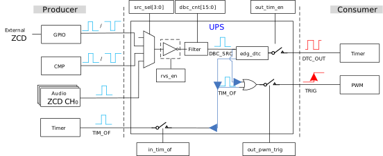
The module supports multiple types of trigger source inputs, including external GPIO zero-crossing detection signals, on-chip comparator output signals, audio channel zero-crossing detection signals, and timer overflow signals. The trigger source can be flexibly switched through the source selection interface. After polarity inversion configuration and digital debounce filtering, the input signals have external signal noise and glitches removed, generating stable valid trigger signals that provide a reliable trigger foundation for dimming synchronization.
Dual-channel Trigger Output and Dimming Synchronization Logic
The stabilized trigger signal is output in two paths, directly supporting the core principle of AC dimming:
One path generates a trigger pulse through edge detection, driving the back-end timer to start counting and realizing the first trigger from an external zero-crossing event. This corresponds to the zero-crossing synchronization node of the AC mains cycle, anchoring the reference for dimming pulse output.
The other path performs OR logic synthesis of the stable trigger signal with the timer overflow feedback signal, outputting a comprehensive trigger signal to drive the PWM module. This both responds to the external zero-crossing first trigger to generate a dimming pulse, and triggers the PWM a second time after the timer expires, generating a second dimming pulse. This precisely matches the dual-pulse control requirement of AC dimming: “zero-crossing synchronization + delayed dimming.”
Core Dimming Principle
The core of AC dimming is to control the phase of the pulse output, adjusting the conduction time within the half-cycle of the mains, thereby changing the average voltage at the load side to achieve brightness adjustment. The UPS module serves as the trigger core, using the AC mains zero-crossing signal as a reference, precisely controlling the delay through the timer, and cooperating with PWM to generate two dimming pulses. This precisely locks the dimming phase interval, ensuring brightness adjustment is completed within the mains synchronization cycle while avoiding light flicker caused by zero-crossing interference, guaranteeing smooth and stable dimming performance.
The block diagram of the UPS module is shown below.
Functional Description
Timer
The timer is primarily used to delay a fixed period after receiving an external stimulus, and then regenerate a stimulus event to the PWM. In the actual circuit, the timer stimulus is not only sent to the PWM but also serves as an input signal for the timer to stop, controlling the timer so that it automatically stops after each timeout overflow.
In practical dimming applications, the timer is often configured at half the mains cycle. For example, under a 50 Hz mains supply, the overflow period of the dimming timer is typically 10 ms.
The following figures show the timer block diagram and the timer timing diagram.
The timer operates as follows:
If the timer detects a high level at the input, the internal counter starts counting up from 0. When a low level is detected, the timer stops operating.
The edg_dtc circuit detects the preceding stimulus signal and triggers the timer to start counting.
If the counter overflows, the of_out overflow signal outputs a high level for one clock cycle. It will be pulled low after one cycle ends.
The edg_dtc circuit detects the of_out pulse signal and triggers the timer to stop counting.
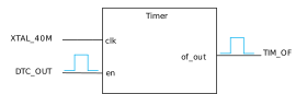
Timer Block Diagram
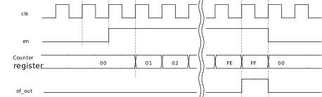
Timer Timing Diagram
In the practical application of UPS, TIM10 is used as the fixed timer.
In the practical application of UPS, TIM10 is used as the fixed timer.
In the practical application of UPS, TIM10 is used as the fixed timer.
In the practical application of UPS, TIM10 is used as the fixed timer.
In the practical application of UPS, TIM10 is used as the fixed timer.
In the practical application of UPS, Basic timer (TIM0~TIM3) is respectively used by PWM timer (TIM4~TIM7) as the fixed timer.
In the practical application of UPS, Basic timer (TIM0~TIM1) is respectively used by PWM timer (TIM4~TIM5) as the fixed timer.
Deglitch Filter and Signal Reverse
To reduce the impact of signal glitches on digital circuits, the deglitch filter uses the XTAL_40MHz sampling clock to debounce the signal. The larger the dbc_cnt value, the wider the glitches that can be filtered, and the longer the delay will be. For different UPS signal sources, adjusting the dbc_cnt value appropriately can filter out glitches while minimizing the delay introduced by digital filtering.
External ZCD signals and CMP outputs can be positive pulse or negative pulse. When the signal is a positive pulse, the system operates normally. When the signal is a negative pulse, configure rvs_en to 1 to reverse the negative pulse signal, ensuring normal system operation.
Edge Detection
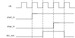
The following figure shows the block diagram of edge detection. The input signals of the edg_dtc module include clk, start_in, and stop_in, and the output is dtc_out.
The edg_dtc module operates as follows:
edg_dtc detects the rising edges of start_in and stop_in.
When a rising edge is detected on start_in, edg_dtc pulls up the dtc_out signal after one clock cycle.
When a rising edge is detected on stop_in, edg_dtc pulls down the dtc_out signal after one clock cycle; otherwise, the dtc_out signal remains high.
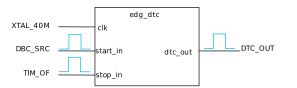
The timing diagram of edge detection is shown in the following figure.
Dimming Signal Types
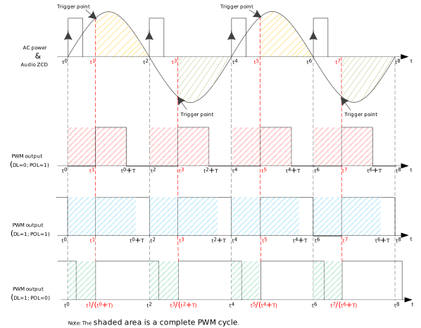
To cooperate with the UPS circuit, the PWM needs to be configured to operate in One Pulse Mode. To meet various demands, parameters such as the default output level of the PWM can be flexibly adjusted during PWM configuration for different control requirements.
OPM_DefaultLevelx = low, CCxPolarity = active_low: Pull down the control signal before the second zero-crossing point.
OPM_DefaultLevelx = high, CCxPolarity = active_low: Pull down the control signal at the second zero-crossing point.
OPM_DefaultLevelx = high, CCxPolarity = active_high: Pull down the control signal after the second zero-crossing point.
Registers
REG_UPS_CTRL
Size: 32
Address: 0x410082C4
Read/write access: R/W
Bit |
Symbol |
Access |
INI |
Description |
|---|---|---|---|---|
31:28 |
UPS_SRC_SEL |
R/W |
0 |
UPS trigger source select:
|
21 |
UPS_OUT_PWM_TRIG |
R/W |
0 |
Enable for output trigger to pwm |
20 |
UPS_OUT_TIM_EN |
R/W |
0 |
Enable for output en signal to basic timer |
19 |
UPS_IN_TIM_OF |
R/W |
0 |
Enable for basic timer overflow input |
18 |
UPS_RVS_EN |
R/W |
0 |
Invert polarity for UPS input
|
17:2 |
UPS_DBC_CNT |
R/W |
0 |
Debounce count for UPS funciton |
REG_PRS_CTRL
Size: 32
Address: 0x4100C2C4
Read/write access: R/W
Bit |
Symbol |
Access |
INI |
Description |
|---|---|---|---|---|
31:28 |
PRS_SRC_SEL |
R/W |
0 |
PRS trigger source select:
|
21 |
PRS_OUT_PWM_TRIG |
R/W |
0 |
Enable for output trigger to pwm |
20 |
PRS_OUT_TIM_EN |
R/W |
0 |
Enable for output en signal to basic timer |
19 |
PRS_IN_TIM_OF |
R/W |
0 |
Enable for basic timer overflow input |
18 |
PRS_RVS_EN |
R/W |
0 |
Invert polarity for PRS input,
|
17:2 |
PRS_DBC_CNT |
R/W |
0 |
Debounce count for PRS funciton |
REGISTER_CONTENTS=RTL8720E
REGISTER_CONTENTS=RTL8720E
REGISTER_CONTENTS=RTL8720E
Not supported.
Base Address: 0x41000A00
Name |
Address offset |
Access |
Description |
|---|---|---|---|
000h |
R/W |
||
004h |
R/W |
||
008h |
R/W |
||
00Ch |
R/W |
||
010h |
R/W |
Dummy register |
REG_UPS_CTRL0
Size: 32
Address offset: 000h
Read/write access: R/W
Bit |
Symbol |
Access |
INI |
Description |
|---|---|---|---|---|
31:28 |
UPS0_SRC_SEL |
R/W |
0 |
UPS trigger source select:
|
27:22 |
RSVD |
R |
- |
Reserved |
21 |
UPS0_OUT_PWM_TRIG |
R/W |
0 |
Enable for output trigger to pwm |
20 |
UPS0_OUT_TIM_EN |
R/W |
0 |
Enable for output en signal to basic timer |
19 |
UPS0_IN_TIM_OF |
R/W |
0 |
Enable for basic timer overflow input |
18 |
UPS0_RVS_EN |
R/W |
0 |
Invert polarity for UPS input
|
17:2 |
UPS0_DBC_CNT |
R/W |
0 |
Debounce count for UPS funciton |
1:0 |
RSVD |
R |
- |
Reserved |
REG_UPS_CTRL1
Size: 32
Address offset: 004h
Read/write access: R/W
Bit |
Symbol |
Access |
INI |
Description |
|---|---|---|---|---|
31:28 |
UPS1_SRC_SEL |
R/W |
0 |
UPS trigger source select:
|
27:22 |
RSVD |
R |
- |
Reserved |
21 |
UPS1_OUT_PWM_TRIG |
R/W |
0 |
Enable for output trigger to pwm |
20 |
UPS1_OUT_TIM_EN |
R/W |
0 |
Enable for output en signal to basic timer |
19 |
UPS1_IN_TIM_OF |
R/W |
0 |
Enable for basic timer overflow input |
18 |
UPS1_RVS_EN |
R/W |
0 |
Invert polarity for UPS input
|
17:2 |
UPS1_DBC_CNT |
R/W |
0 |
Debounce count for UPS funciton |
1:0 |
RSVD |
R |
- |
Reserved |
REG_UPS_CTRL2
Size: 32
Address offset: 008h
Read/write access: R/W
Bit |
Symbol |
Access |
INI |
Description |
|---|---|---|---|---|
31:28 |
UPS2_SRC_SEL |
R/W |
0 |
UPS trigger source select:
|
27:22 |
RSVD |
R |
- |
Reserved |
21 |
UPS2_OUT_PWM_TRIG |
R/W |
0 |
Enable for output trigger to pwm |
20 |
UPS2_OUT_TIM_EN |
R/W |
0 |
Enable for output en signal to basic timer |
19 |
UPS2_IN_TIM_OF |
R/W |
0 |
Enable for basic timer overflow input |
18 |
UPS2_RVS_EN |
R/W |
0 |
Invert polarity for UPS input
|
17:2 |
UPS2_DBC_CNT |
R/W |
0 |
Debounce count for UPS funciton |
1:0 |
RSVD |
R |
- |
Reserved |
REG_UPS_CTRL3
Size: 32
Address offset: 00Ch
Read/write access: R/W
Bit |
Symbol |
Access |
INI |
Description |
|---|---|---|---|---|
31:28 |
UPS3_SRC_SEL |
R/W |
0 |
UPS trigger source select:
|
27:22 |
RSVD |
R |
- |
Reserved |
21 |
UPS3_OUT_PWM_TRIG |
R/W |
0 |
Enable for output trigger to pwm |
20 |
UPS3_OUT_TIM_EN |
R/W |
0 |
Enable for output en signal to basic timer |
19 |
UPS3_IN_TIM_OF |
R/W |
0 |
Enable for basic timer overflow input |
18 |
UPS3_RVS_EN |
R/W |
0 |
Invert polarity for UPS input
|
17:2 |
UPS3_DBC_CNT |
R/W |
0 |
Debounce count for UPS funciton |
1:0 |
RSVD |
R |
- |
Reserved |
REG_PRS_DUMMY
Name: PRS Dummy Register
Size: 32
Address offset: 010h
Read/write access: R/W
Dummy register
Bit |
Symbol |
Access |
INI |
Description |
|---|---|---|---|---|
31:0 |
DUMMY |
R/W |
ffffh |
Dummy register |
Base Address: 0x401C7A00
Name |
Address offset |
Access |
Description |
|---|---|---|---|
000h |
R/W |
||
004h |
R/W |
||
010h |
R/W |
Dummy register |
REG_UPS_CTRL0
Size: 32
Address offset: 000h
Read/write access: R/W
Bit |
Symbol |
Access |
INI |
Description |
|---|---|---|---|---|
31:28 |
UPS0_SRC_SEL |
R/W |
0 |
UPS trigger source select:
|
27:22 |
RSVD |
R |
- |
Reserved |
21 |
UPS0_OUT_PWM_TRIG |
R/W |
0 |
Enable for output trigger to pwm |
20 |
UPS0_OUT_TIM_EN |
R/W |
0 |
Enable for output en signal to basic timer |
19 |
UPS0_IN_TIM_OF |
R/W |
0 |
Enable for basic timer overflow input |
18 |
UPS0_RVS_EN |
R/W |
0 |
Invert polarity for UPS input
|
17:2 |
UPS0_DBC_CNT |
R/W |
0 |
Debounce count for UPS funciton |
1:0 |
RSVD |
R |
- |
Reserved |
REG_UPS_CTRL1
Size: 32
Address offset: 004h
Read/write access: R/W
Bit |
Symbol |
Access |
INI |
Description |
|---|---|---|---|---|
31:28 |
UPS1_SRC_SEL |
R/W |
0 |
UPS trigger source select:
|
27:22 |
RSVD |
R |
- |
Reserved |
21 |
UPS1_OUT_PWM_TRIG |
R/W |
0 |
Enable for output trigger to pwm |
20 |
UPS1_OUT_TIM_EN |
R/W |
0 |
Enable for output en signal to basic timer |
19 |
UPS1_IN_TIM_OF |
R/W |
0 |
Enable for basic timer overflow input |
18 |
UPS1_RVS_EN |
R/W |
0 |
Invert polarity for UPS input
|
17:2 |
UPS1_DBC_CNT |
R/W |
0 |
Debounce count for UPS funciton |
1:0 |
RSVD |
R |
- |
Reserved |
REG_PRS_DUMMY
Name: PRS Dummy Register
Size: 32
Address offset: 010h
Read/write access: R/W
Dummy register
Bit |
Symbol |
Access |
INI |
Description |
|---|---|---|---|---|
31:0 |
DUMMY |
R/W |
ffffh |
Dummy register |