General-purpose I/Os (GPIO)
Introduction
The GPIO module is a programmable peripheral that provides flexible control of external I/O pad signals.
The chip integrates multiple independent GPIO controllers, organized as PORT_A, PORT_B, etc. Each port supports the following primary per-pin functions: direction control (input or output), output data control and input state readback via memory-mapped registers, and external interrupt detection for event-driven system response. Within each port, every pin operates independently, allowing fine-grained configuration and monitoring of I/O signals.
Each port contains multiple groups of registers, including basic I/O control registers (GPIO_DR, GPIO_DDR, GPIO_EXT_PORT), interrupt control registers (GPIO_INT_XXX), and debounce control register (GPIO_DB_DIV_CONFIG). The debounce function is controlled at the group level, while all other registers provide bit-level control, with each bit corresponding to an individual GPIO pin.
Features
Up to 64 pins
PortA: PA0 ~ PA31
PortB: PB0 ~ PB31
Up to 52 pins
PortA: PA0 ~ PA31
PortB: PB0 ~ PB19
Up to 52 pins
PortA: PA0 ~ PA31
PortB: PB0 ~ PB19
Up to 52 pins
PortA: PA0 ~ PA31
PortB: PB0 ~ PB19
Up to 52 pins
PortA: PA0 ~ PA31
PortB: PB0 ~ PB19
Up to 96 pins
PortA: PA0 ~ PA31
PortB: PB0 ~ PB31
PortC: PC0 ~ PC31
Up to 94 pins
PortA: PA0 ~ PA31
PortB: PB0 ~ PB31
PortC: PC0 ~ PC29
Output race condition protection
Up to 37 pins
PortA: PA0 ~ PA31
PortB: PB0 ~ PB4
Output race condition protection
Independent register control
Separate data register and data direction register for each GPIO signal
Flexible interrupt modes
Selectable level-sensitive interrupt detection
Selectable edge-triggered interrupt detection
Debounce capability
Configurable debounce circuitry with slow clock source
Effective noise filtering for interrupt pins
Block Diagram
The block diagram of GPIO is illustrated below.

The GPIO block consists of the following main functional interface groups:
APB Interface: Connects to the APB bridge for memory-mapped register access, enabling software configuration and control of GPIO functionality.
External Data Interface: Interfaces directly with physical I/O pads to drive output signals or sample input data from external pins.
Interrupt Interface: Generates interrupt requests to the system interrupt controller when configured GPIO events occur, and receives interrupt acknowledgment signals.
Functional Description
This section describes the functional operation of the GPIO.
Direction Control
The direction of each external I/O pad is programmed through the corresponding PORTx data direction register (GPIO_DDR). Each bit in GPIO_DDR independently controls the direction (input or output) of its associated signal. The GPIO_DDR register is accessible to the processor via the APB bus interface.
The data and control flow architecture is illustrated in the following block diagram.

Within GPIO_DDR, each bit is individually controllable, so the register effectively provides N independent direction control bits for a PORTx GPIO bus of width N (bit index range 0 to N-1).
For each bit in GPIO_DDR:
Writing
1configures the corresponding I/O pad as an output.Writing
0configures the corresponding I/O pad as an input.
Data Output
When a GPIO pin is configured as an output, data written to the PORTx data register (GPIO_DR) directly drives the output buffer of the corresponding I/O pad on a per-bit basis.
Each bit in GPIO_DR controls one output signal:
Writing
1drives the corresponding I/O pad output high.Writing
0drives the corresponding I/O pad output low.
Race Condition Protection
Not supported.
Not supported.
Not supported.
Not supported.
Not supported.
Not supported.
GPIOs are organized into ports, with each port typically containing up to multiple GPIO pins that share a single output value register. As the output state of an individual pin cannot be modified atomically, a read-modify-write sequence is required to update a single GPIO output. This introduces a potential race condition in multi-tasking or multi-threaded environments, where concurrent access to the same port may lead to unexpected pin states.
To resolve this issue, the chip implements hardware-level race condition protection controlled by register bit 0x4080A2C4[31]. When this bit is not set, the output is controlled directly by GPIO_DR in normal output mode. When this bit is set, the control logic behaves as follows:
Writing
1toggles the bit value and inverts the I/O pad output.Writing
0preserves the bit value and maintains the I/O pad output.
GPIOs are organized into ports, with each port typically containing up to multiple GPIO pins that share a single output value register. As the output state of an individual pin cannot be modified atomically, a read-modify-write sequence is required to update a single GPIO output. This introduces a potential race condition in multi-tasking or multi-threaded environments, where concurrent access to the same port may lead to unexpected pin states.
To resolve this issue, the chip implements hardware-level race condition protection controlled by register bit 0x408012C4[31]. When this bit is not set, the output is controlled directly by GPIO_DR in normal output mode. When this bit is set, the control logic behaves as follows:
Writing
1toggles the bit value and inverts the I/O pad output.Writing
0preserves the bit value and maintains the I/O pad output.
Data Input
The level status of external pins can be obtained by reading the GPIO_EXT_PORT register via the APB bus. Regardless of whether the pin is configured as input or output mode, the readback value of this register corresponds to the logic value of the actual level of the external pin.
Note
When GPIO is configured as output mode and GPIO_DR outputs high level (logic value 1), if the external pin is connected to a low level (such as GND), reading GPIO_EXT_PORT will return 0, indicating that the external pin is actually in a low level state.
The GPIO_EXT_PORT register is read-only, meaning that it cannot be written from the APB software interface.
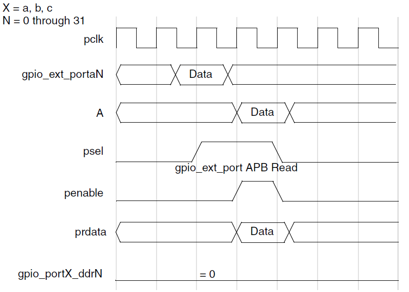
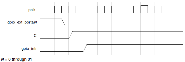
The following figure shows a timing diagram of a read to the GPIO_EXT_PORT memory map registers when the direction is set to input and the metastability registers are included, which brings a data delay of the port line.
Note
The maximum data rate that can be read back on consecutive reads from GPIO_EXT_PORT must be less than PCLK/2. Two pclk cycles per read access is required due to the non-pipelined nature of the APB. The assumption is that the APB bridge does not lose ownership of the AHB during consecutive accesses when PCLK=HCLK.
Interrupts
The GPIO peripheral supports configurable interrupt sources on any GPIO pin, with programmable interrupt types:
Edge-triggered interrupts: Rising edge, falling edge, or both edges
Level-sensitive interrupts: Active-high or active-low level
Interrupt masking is implemented through the GPIO_INT_MASK register, providing both masked (GPIO_INT_STATUS) and raw (GPIO_INT_STATUS_RAW) interrupt status information. Interrupt configuration requires the GPIO port data direction to be set as Input. Reprogramming the direction to Output preserves pending interrupts but prevents new interrupt generation.
The following figure illustrates the interrupt generation and data flow, showing two possible output architectures:
Individual Interrupt Mode: Separate signals (gpio_intr[N] or gpio_intr_n[N])
Combined Interrupt Mode: Single unified signal (gpio_intr_flag or gpio_intr_flag_n)
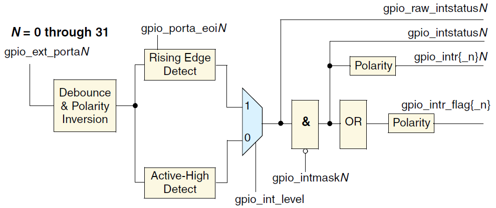
Interrupt RTL block diagram
In combined mode, the interrupt signal is generated by logically ORing all individual interrupt lines. This chip implements the combined interrupt architecture. Each GPIO port has one dedicated IRQ number in the system interrupt controller. Due to the combined interrupt implementation, the ISR must read the GPIO_INT_STATUS register to identify which GPIO pin(s) triggered the interrupt. The processor is responsible for interrupt prioritization and handling through software.
Interrupt Synchronization
Interrupt signals can be internally synchronized to a dedicated system clock, pclk_intr, with synchronization requirements determined by the interrupt type:
Edge-sensitive interrupts: Synchronization to pclk_intr is required. Edge-detected interrupt signals delivered to the processor are guaranteed to be synchronous with the system bus clock.
Level-sensitive interrupts: Synchronization to pclk_intr is optional and configurable through the GPIO_INT_LS_SYNC register by software.
The pclk_intr signal serves a critical role in power-managed systems. If the system requires interrupt detection capability even when the GPIO pclk is gated off, then pclk_intr must be provided. It is assumed that pclk_intr operates synchronously with pclk. Conversely, if interrupt detection is only required when pclk is running, both pclk_intr and pclk can be connected to the same clock source.
Edge-Sensitive Interrupt
Edge-sensitive interrupts are cleared by writing to the GPIO_INT_EOI register, which simultaneously clears both interrupt and raw status registers. Clearing the interrupt source before writing to GPIO_INT_EOI is recommended. This register has no effect on level-sensitive interrupts. In combined interrupt configurations, multiple edge-detected interrupts can be cleared simultaneously.
Single Edge Detection
The following figure shows an RTL diagram of the synchronization and edge detection of interrupt sources on gpio_ext_portaN signals, when GPIO_INT_BOTH_EDGE =0.
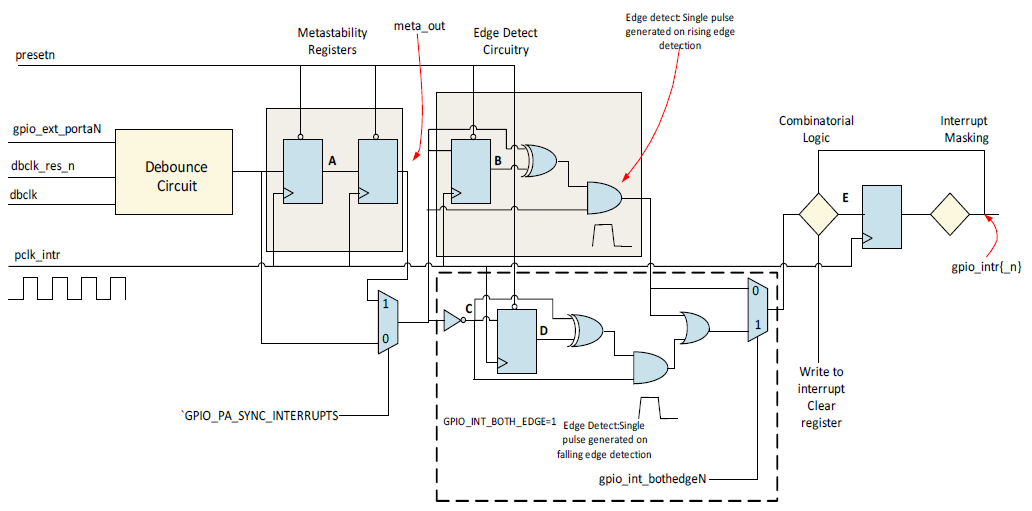
Synchronization and edge detect interrupt generation (GPIO_INT_BOTH_EDGE=0)
Note
Metastability part is default included.
Figure GPIO interrupt metastable shows a timing diagram in which an interrupt is generated on the rising edge of input on Port A; this is where the debounce logic is disabled and metastability registers are included. It also shows how an interrupt is cleared by a write to the interrupt clear register.
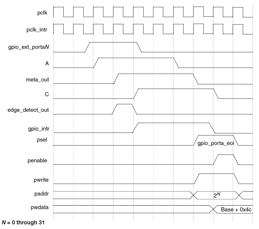
Interrupt edge detection and interrupt clear timing (GPIO_SYNC_PA_INTERRUPTS = 1, metastability included)
A case may arise where the Interrupt Service Routine (ISR) writes to the interrupt clear register to clear an existing interrupt during the same clock cycle in which a new interrupt is detected. In such a case, writing to the interrupt clear register clears only the first interrupt. The second interrupt is not lost, since setting an interrupt has a higher priority than clearing it.
Figure GPIO interrupt stable shows a timing diagram similar to the figure Figure GPIO interrupt metastable except that metastability registers are removed. It also shows how an interrupt is cleared by a write to the interrupt clear register.
Note
Since the Metastability registers are removed from the path, A and B waveforms, shown in Figure GPIO interrupt metastable, no longer exist, and all subsequent signal delays are reduced by two clock cycles.
Interrupt edge detection and interrupt clear timing (GPIO_SYNC_PA_INTERRUPTS = 0, metastability removed)
The following figure shows such a case where the debounce logic is unused. In this timing diagram, meta_out and edge_detect_out are the outputs of the second metastability register and the edge detect logic, respectively. The second edge detection occurs on the same cycle as the write to the interrupt clear register. In this example, the write to the interrupt clear register does not clear the second interrupt, and the gpio_intr{_n} signal is not de-asserted.
Write to interrupt clear register, coincident with detection of new interrupt
Dual Edge Detection
Interrupt detection logic for both the rising edge and the falling edge is available only when the GPIO_INT_BOTHEDGE register is programmed to 1 and this logic detects the interrupt on both the rising edge and the falling edge.
The following figure shows the synchronization and edge detect interrupt generation of the interrupt sources on gpio_ext_portaN signals.

Synchronization and edge detect interrupt generation (GPIO_INT_BOTH_EDGE=1)
The following figure shows a timing diagram where an interrupt is generated on both the rising edge and the falling edge of input on Port A, that is, with GPIO_INT_BOTH_EDGE = 1 and GPIO_INT_BOTHEDGE programmed to detect both edges.
In this scenario, debounce logic is disabled and metastability registers are included. This figure also shows how an interrupt is cleared by a write to the interrupt clear register.

Interrupt edge detection and interrupt clear timing (GPIO_SYNC_PA_INTERRUPTS = 1 and GPIO_INT_BOTH_EDGE =1, metastability included)
The following figure shows a timing diagram similar to the figure Figure interrupt_metastability_included, except that in this scenario, metastability registers are removed.
Interrupt edge detection and interrupt clear timing (GPIO_SYNC_PA_INTERRUPTS = 0 and GPIO_INT_BOTH_EDGE =1, metastability removed)
Level-Sensitive Interrupt
Level-sensitive interrupts require proper interrupt service routine (ISR) handling. The ISR can either poll the GPIO_INT_STATUS_RAW register until the interrupt source clears or mask the interrupt via GPIO_INT_MASK before exiting.
If the ISR exits without masking, the level-sensitive interrupt will repeatedly trigger until the source condition is resolved.
The following figure shows the generation of level-sensitive interrupts. As well, the debounce circuit below is an example of debounce or remove spurious glitches of less than 2 cycles of dbclk.
Level-sensitive interrupt RTL diagram
With level-sensitive interrupts, there is a choice of whether they are synchronized to the interrupt clock pclk_intr or are entirely combinational (aside from the debounce circuit).
The selection is done by programming the GPIO_INT_LS_SYNC (GPIO Level-Sensitive Synchronous) register.
This is a memory-mapped bit that inserts two metastability registers clocked off of pclk_intr to synchronize the level-sensitive interrupts to pclk_intr.
When GPIO_INT_LS_SYNC is not asserted, there is no guarantee that the interrupt lines are synchronous to pclk_intr. A processor status register may need to be set to indicate asynchronous interrupts. When GPIO_INT_LS_SYNC is asserted, the pclk_intr clock must be present to pass the interrupt to the interrupt controller block.
The gpio_intrclk_en output signal is asserted when level-sensitive interrupts are selected for synchronization to pclk_intr. The gpio_intrclk_en signal can be used in the clock generation block to turn on pclk_intr.
Note
In active mode, synchronizing pclk_intr to pclk is recommended to prevent circuit burrs.
In sleep mode, disabling this synchronization allows faster wake-up if required.
The following figure shows the generation of an active-low level-sensitive interrupt where the debounce circuitry is disabled.
Active-low level-sensitive interrupt generation timing
Debounce Operation
If the user has configured the interrupt feature, GPIO can be configured to either include or exclude a debounce capability using the GPIO_DEBOUNCE parameter. The external signal can be debounced to remove any spurious glitches that are less than one period of the external debouncing clock.
The following figure shows an RTL diagram of the debounce circuitry. The timing diagram shows an active-high input signal on gpio_ext_portxN. The polarity of the input signal detection is controlled by the memory-mapped signal, gpio_int_polarity. For a falling-edge or active-low-sensitive input, the input is then inverted and the same debounce logic is used as for rising-edge or active-high level-sensitive interrupts.
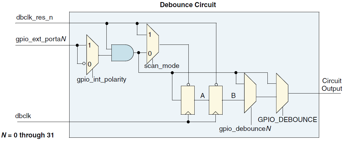
Debounce RTL diagram
dbclk_res_n signal is asynchronously asserted and synchronously de-asserted to the debounce clock, dbclk.
presetn, the system reset signal, is asynchronously asserted and synchronously de-asserted to pclk; synchronization must be external to the component.
The pclk and dbclk signals are assumed to be asynchronous to each other.
When input interrupt signals are debounced using a debounce clock, the signals must be active for a minimum of two cycles of the debounce clock to guarantee that they are registered. Any input pulse widths less than a debounce clock period are bounced. A pulse width between one and two debounce clock widths may or may not propagate, depending on its phase relationship to the debounce clock. If the input pulse spans two rising edges of the debounce clock, it is registered. If it spans only one rising edge, it is not registered.
The timing diagram below shows both cases: the input signal being bounced, and later, a propagated input signal. If GPIO supports debounce, then debouncing input signals on Port A can be enabled or disabled under software control.
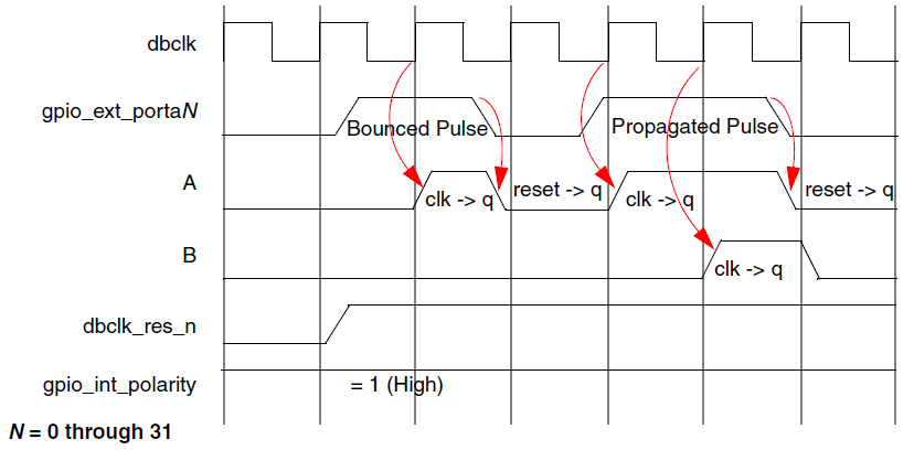
Debounce timing with asynchronous reset flip-flops
Note
The use of the debounce circuitry increases interrupt latency by two clock cycles of the debounce clock.
The debounce circuitry works with only asynchronous reset flip-flops.
Registers
Base Address: 0x41010000
Name |
Address offset |
Access |
Description |
|---|---|---|---|
000h |
R/W |
||
004h |
R/W |
||
008h |
R |
||
030h |
R/W |
||
038h |
R/W |
||
03Ch |
R/W |
||
040h |
R |
||
044h |
R |
||
048h |
R/W |
||
04Ch |
R/W |
||
050h |
R |
||
060h |
R/W |
||
064h |
R |
||
068h |
R/W |
||
06Ch |
R |
||
078h |
R |
REG_GPIO_DR
Name: PortA/B data register
Size: 32
Address offset: 000h
Read/write access: R/W
Bit |
Symbol |
Access |
INI |
Description |
|---|---|---|---|---|
31:0 |
PORT_DATA |
R/W |
0 |
Values written to this register are output on the I/O signals for Portx if the corresponding data direction bits for Portx are set to output mode and the corresponding control bit for Portx is set to software mode. The value read back equals to the last value written to this register. |
REG_GPIO_DDR
Name: PortA/B data direction register
Size: 32
Address offset: 004h
Read/write access: R/W
Bit |
Symbol |
Access |
INI |
Description |
|---|---|---|---|---|
31:0 |
PORT_DATA_DIRECTION |
R/W |
0 |
Values written to this register independently control the direction of the corresponding data bit in Portx. The default direction can be configured as input or output after system reset through the GPIO_DFLT_DIR_x parameter.
|
REG_GPIO_CTL
Name: PortA/B data source register
Size: 32
Address offset: 008h
Read/write access: R
Bit |
Symbol |
Access |
INI |
Description |
|---|---|---|---|---|
31:0 |
RSVD |
R |
- |
Reserved |
REG_GPIO_INT_EN
Name: PortA/B interrupt enable register
Size: 32
Address offset: 030h
Read/write access: R/W
Bit |
Symbol |
Access |
INI |
Description |
|---|---|---|---|---|
31:0 |
GPIO_INT_EN |
R/W |
0 |
Allows each bit of Portx to be configured for interrupts. By default, the generation of interrupts is disabled. Whenever a 1 is written to a bit of this register, it configures the corresponding bit on Portx to become an interrupt; otherwise, Portx operates as a normal GPIO signal. Interrupts are disabled on the corresponding bits of Portx if the corresponding data direction register is set to output or if Portx mode is set to hardware.
|
REG_GPIO_INT_TYPE
Name: PortA/B interrupt trigger type register
Size: 32
Address offset: 038h
Read/write access: R/W
Bit |
Symbol |
Access |
INI |
Description |
|---|---|---|---|---|
31:0 |
GPIO_INT_TYPE |
R/W |
0 |
Controls the type of interrupt that can occur on Portx. Whenever a 0 is written to a bit of this register, it configures the interrupt type to be level-sensitive; otherwise, it is edge-sensitive.
|
REG_GPIO_INT_POLARITY
Name: PortA/B interrupt polarity register
Size: 32
Address offset: 03Ch
Read/write access: R/W
Bit |
Symbol |
Access |
INI |
Description |
|---|---|---|---|---|
31:0 |
GPIO_INT_POLARITY |
R/W |
0 |
Controls the polarity of edge or level sensitivity that can occur on input of Portx. Whenever a 0 is written to a bit of this register, it configures the interrupt type to falling-edge or active-low sensitive; otherwise, it is rising-edge or active-high sensitive.
|
REG_GPIO_INT_STATUS
Name: PortA/B interrupt status register
Size: 32
Address offset: 040h
Read/write access: R
Bit |
Symbol |
Access |
INI |
Description |
|---|---|---|---|---|
31:0 |
GPIO_INT_STATUS |
R |
0 |
Interrupt status of Portx. |
REG_GPIO_INT_STATUS_RAW
Name: PortA/B raw interrupt status register
Size: 32
Address offset: 044h
Read/write access: R
Bit |
Symbol |
Access |
INI |
Description |
|---|---|---|---|---|
31:0 |
GPIO_RAW_INT_STATUS |
R |
0 |
Raw interrupt status of Portx (premasking bits). |
REG_GPIO_DEBOUNCE
Name: PortA/B interrupt debounce register
Size: 32
Address offset: 048h
Read/write access: R/W
Bit |
Symbol |
Access |
INI |
Description |
|---|---|---|---|---|
31:0 |
GPIO_DEBOUNCE_EN |
R/W |
0 |
Controls whether an external signal that is the source of an interrupt needs to be debounced to remove any spurious glitches. Writing a 1 to a bit in this register enables the debouncing circuitry. A signal must be valid for two periods of an external clock before it is internally processed.
This register is available only if Portx is configured to generate interrupts (GPIO_PORTA_INTR = Include(1)) and when the debounce logic is included (GPIO_DEBOUNCE = Include(1)). |
REG_GPIO_INT_EOI
Name: PortA/B edge type interrupt clear register
Size: 32
Address offset: 04Ch
Read/write access: R/W
Bit |
Symbol |
Access |
INI |
Description |
|---|---|---|---|---|
31:0 |
GPIO_INT_EOI |
R/W |
0 |
Controls the clearing of edge type interrupts from Portx. When a 1 is written into a corresponding bit of this register, the interrupt is cleared. All interrupts are cleared when Portx is not configured for interrupts.
|
REG_GPIO_EXT_PORT
Name: External PortA/B data register
Size: 32
Address offset: 050h
Read/write access: R
Bit |
Symbol |
Access |
INI |
Description |
|---|---|---|---|---|
31:0 |
GPIO_EXT_PORTA |
R |
0 |
When Portx is configured as Input, then reading this location reads the values on the signal. When the data direction of Portx is set as output, reading this location reads the data register for Portx. |
REG_GPIO_ITN_LS_SYNC
Name: PortA/B level interrupt synchronization
Size: 32
Address offset: 060h
Read/write access: R/W
Bit |
Symbol |
Access |
INI |
Description |
|---|---|---|---|---|
31:1 |
RSVD |
R |
- |
Reserved |
0 |
GPIO_LEVEL_SYNC |
R/W |
0 |
Writing a 1 to this register results in all level-sensitive interrupts being synchronized to pclk_intr.
|
REG_GPIO_ID_CODE
Name: PortA/B GPIO ID code register
Size: 32
Address offset: 064h
Read/write access: R
Bit |
Symbol |
Access |
INI |
Description |
|---|---|---|---|---|
31:0 |
GPIO_ID_CODE |
R |
32’h1 |
This register is available only if Portx is configured to generate interrupts (GPIO_PORTx_INTR = Include(1)) and interrupt detection is configured to generate on both rising and falling edges of external input signal (GPIO_INT_BOTH_EDGE=Include(1)). |
REG_GPIO_INT_BOTHEDGE
Name: PortA/B both edge interrupt register
Size: 32
Address offset: 068h
Read/write access: R/W
Bit |
Symbol |
Access |
INI |
Description |
|---|---|---|---|---|
31:0 |
GPIO_INT_BOTHEDGE |
R/W |
0 |
Controls the edge types of interrupt that can occur on Portx. Whenever a particular bit is programmed to 1, it enables the generation of interrupt on both the rising edge and falling edge of an external input signal corresponding to that bit on Portx. The values programmed in the registers gpio_intype_level and gpio_int_polarity for this particular bit are not considered when the corresponding bit of this register is set to 1. Whenever a particular bit is programmed to 0, the interrupt type depends on the value of the corresponding bits in the gpio_inttype_level and gpio_int_polarity registers.
|
REG_GPIO_VER_ID_CODE
Name: PortA/B GPIO component version register
Size: 32
Address offset: 06Ch
Read/write access: R
Bit |
Symbol |
Access |
INI |
Description |
|---|---|---|---|---|
31:0 |
GPIO_VER_ID_CODE |
R |
32’h3231302A |
ASCII value for each number in the version, followed by *. For example, 32_30_31_2A represents the version 2.01*. |
REG_GPIO_DB_DIV_CONFIG
Size: 32
Address offset: 078h
Read/write access: R
Bit |
Symbol |
Access |
INI |
Description |
|---|---|---|---|---|
31:0 |
RSVD |
R |
- |
Reserved |
Base Address: 0x4101A000
Name |
Address offset |
Access |
Description |
|---|---|---|---|
000h |
R/W |
||
004h |
R/W |
||
008h |
R |
||
030h |
R/W |
||
034h |
R/W |
||
038h |
R/W |
||
03Ch |
R/W |
||
040h |
R |
||
044h |
R |
||
048h |
R/W |
||
04Ch |
R/W |
||
050h |
R |
||
060h |
R/W |
||
064h |
R |
||
068h |
R/W |
||
06Ch |
R |
REG_GPIO_DR
Name: PortA/B data register
Size: 32
Address offset: 000h
Read/write access: R/W
Bit |
Symbol |
Access |
INI |
Description |
|---|---|---|---|---|
31:0 |
PORT_DATA |
R/W |
0 |
Values written to this register are output on the I/O signals for Portx if the corresponding data direction bits for Portx are set to Output mode and the corresponding control bit for Portx is set to software mode. The value read back is equal to the last value written to this register. Valid bits is: PortA[31:0] and PortB[19:0]. |
REG_GPIO_DDR
Name: PortA/B data direction register
Size: 32
Address offset: 004h
Read/write access: R/W
Bit |
Symbol |
Access |
INI |
Description |
|---|---|---|---|---|
31:0 |
PORT_DATA_DIRECTION |
R/W |
0 |
Values written to this register independently control the direction of the corresponding data bit in Portx. The default direction can be configured as input or output after system reset through the GPIO_DFLT_DIR_x parameter.
Valid bits is: PortA[31:0] and PortB[19:0]. |
REG_GPIO_CTL
Name: PortA/B data source register
Size: 32
Address offset: 008h
Read/write access: R
Bit |
Symbol |
Access |
INI |
Description |
|---|---|---|---|---|
31:0 |
RSVD |
R |
- |
Reserved |
REG_GPIO_INT_EN
Name: PortA/B interrupt enable register
Size: 32
Address offset: 030h
Read/write access: R/W
Bit |
Symbol |
Access |
INI |
Description |
|---|---|---|---|---|
31:0 |
GPIO_INT_EN |
R/W |
0 |
Allows each bit of Portx to be configured for interrupts. By default, the generation of interrupts is disabled. Whenever a 1 is written to a bit of this register, it configures the corresponding bit on Portx to become an interrupt; otherwise, Portx operates as a normal GPIO signal. Interrupts are disabled on the corresponding bits of Portx if the corresponding data direction register is set to Output or if Portx mode is set to Hardware.
|
REG_GPIO_INT_MASK
Name: PortA/B interrupt mask register
Size: 32
Address offset: 034h
Read/write access: R/W
Bit |
Symbol |
Access |
INI |
Description |
|---|---|---|---|---|
31:0 |
GPIO_INT_MASK |
R/W |
0 |
Controls whether an interrupt on Portx can create an interrupt for the interrupt controller by not masking it. By default, all interrupts bits are unmasked. Whenever a 1 is written to a bit in this register, it masks the interrupt generation capability for this signal; otherwise interrupts are allowed through. The unmasked status can be read as well as the resultant status after masking.
|
REG_GPIO_INT_TYPE
Name: PortA interrupt trigger type register
Size: 32
Address offset: 038h
Read/write access: R/W
Bit |
Symbol |
Access |
INI |
Description |
|---|---|---|---|---|
31:0 |
GPIO_INT_TYPE |
R/W |
0 |
Controls the type of interrupt that can occur on Portx. Whenever a 0 is written to a bit of this register, it configures the interrupt type to be level-sensitive; otherwise, it is edge-sensitive.
|
REG_GPIO_INT_POLARITY
Name: PortA interrupt polarity register
Size: 32
Address offset: 03Ch
Read/write access: R/W
Bit |
Symbol |
Access |
INI |
Description |
|---|---|---|---|---|
31:0 |
GPIO_INT_POLARITY |
R/W |
0 |
Controls the polarity of edge or level sensitivity that can occur on input of Portx. Whenever a 0 is written to a bit of this register, it configures the interrupt type to falling-edge or active-low sensitive; otherwise, it is rising-edge or active-high sensitive.
|
REG_GPIO_INT_STATUS
Name: PortA/B interrupt status register
Size: 32
Address offset: 040h
Read/write access: R
Bit |
Symbol |
Access |
INI |
Description |
|---|---|---|---|---|
31:0 |
GPIO_INT_STATUS |
R |
0 |
Interrupt status of Portx. |
REG_GPIO_INT_STATUS_RAW
Name: PortA/B raw interrupt status register
Size: 32
Address offset: 044h
Read/write access: R
Bit |
Symbol |
Access |
INI |
Description |
|---|---|---|---|---|
31:0 |
GPIO_RAW_INT_STATUS |
R |
0 |
Raw interrupt status of Portx (premasking bits). |
REG_GPIO_DEBOUNCE
Name: PortA/B interrupt debounce register
Size: 32
Address offset: 048h
Read/write access: R/W
Bit |
Symbol |
Access |
INI |
Description |
|---|---|---|---|---|
31:0 |
GPIO_DEBOUNCE_EN |
R/W |
0 |
Controls whether an external signal that is the source of an interrupt needs to be debounced to remove any spurious glitches. Writing a 1 to a bit in this register enables the debouncing circuitry. A signal must be valid for two periods of an external clock before it is internally Processed.
This register is available only if Portx is configured to generate interrupts (GPIO_PORTA_INTR = Include (1)) and when the debounce logic is included (GPIO_DEBOUNCE = Include (1)). |
REG_GPIO_INT_EOI
Name: PortA/B edge type interrupt clear register
Size: 32
Address offset: 04Ch
Read/write access: R/W
Bit |
Symbol |
Access |
INI |
Description |
|---|---|---|---|---|
31:0 |
GPIO_INT_EOI |
R/W |
0 |
Controls the clearing of edge type interrupts from Portx. When a 1 is written into a corresponding bit of this register, the interrupt is cleared. All interrupts are cleared when Portx is not configured for interrupts.
|
REG_GPIO_EXT_PORT
Name: External PortA/B data register
Size: 32
Address offset: 050h
Read/write access: R
Bit |
Symbol |
Access |
INI |
Description |
|---|---|---|---|---|
31:0 |
GPIO_EXT_PORTA |
R |
0 |
When Portx is configured as Input, then reading this location reads the values on the signal. When the data direction of Portx is set as Output, reading this location reads the data register for Portx. |
REG_GPIO_ITN_LS_SYNC
Name: PortA/B level interrupt synchronization
Size: 32
Address offset: 060h
Read/write access: R/W
Bit |
Symbol |
Access |
INI |
Description |
|---|---|---|---|---|
31:1 |
RSVD |
R |
- |
Reserved |
0 |
GPIO_LEVEL_SYNC |
R/W |
0 |
Writing a 1 to this register results in all level-sensitive interrupts being synchronized to pclk_intr.
|
REG_GPIO_ID_CODE
Name: PortA/B GPIO ID code register
Size: 32
Address offset: 064h
Read/write access: R
Bit |
Symbol |
Access |
INI |
Description |
|---|---|---|---|---|
31:0 |
GPIO_ID_CODE |
R |
32’h1 |
This register is available only if PortxA/B is configured to generate interrupts (GPIO_PORTx_INTR = Include (1)) and interrupt detection is configured to generate on both rising and falling edges of external input signal (GPIO_INT_BOTH_EDGE=Include (1)). |
REG_GPIO_INT_BOTHEDGE
Name: PortA/B both edge interrupt register
Size: 32
Address offset: 068h
Read/write access: R/W
Bit |
Symbol |
Access |
INI |
Description |
|---|---|---|---|---|
31:0 |
GPIO_INT_BOTHEDGE |
R/W |
0 |
Controls the edge types of interrupt that can occur on Portx. Whenever a particular bit is programmed to 1, it enables the generation of interrupt on both the rising edge and falling edge of an external input signal corresponding to that bit on PortA. The values programmed in the registers gpio_intype_level and gpio_int_polarity for this particular bit are not considered when the corresponding bit of this register is set to 1. Whenever a particular bit is programmed to 0, the interrupt type depends on the value of the corresponding bits in the gpio_inttype_level and gpio_int_polarity registers.
|
REG_GPIO_VER_ID_CODE
Name: PortA/B GPIO component version register
Size: 32
Address offset: 06Ch
Read/write access: R
Bit |
Symbol |
Access |
INI |
Description |
|---|---|---|---|---|
31:0 |
GPIO_VER_ID_CODE |
R |
32’h3231302A |
ASCII value for each number in the version, followed by *. For example 32_30_31_2A represents the version 2.01*. Reset Value: See the releases table in the Release Notes. |
REGISTER_CONTENTS=RTL8720E
REGISTER_CONTENTS=RTL8720E
REGISTER_CONTENTS=RTL8720E
Base Address: 0x4200D000
Name |
Address offset |
Access |
Description |
|---|---|---|---|
000h |
R/W |
||
004h |
R/W |
||
008h |
R |
||
030h |
R/W |
||
034h |
R/W |
||
038h |
R/W |
||
03Ch |
R/W |
||
040h |
R |
||
044h |
R |
||
048h |
R/W |
||
04Ch |
R/W |
||
050h |
R |
||
060h |
R/W |
||
064h |
R |
||
068h |
R/W |
||
06Ch |
R |
||
078h |
R/W |
REG_GPIO_DR
Name: PortA data register
Size: 32
Address offset: 000h
Read/write access: R/W
Bit |
Symbol |
Access |
INI |
Description |
|---|---|---|---|---|
31:0 |
PORTA_DATA |
R/W |
0 |
Values written to this register are output on the I/O signals for Portx if the corresponding data direction bits for Portx are set to Output mode and the corresponding control bit for Portx is set to software mode. The value read back is equal to the last value written to this register. |
REG_GPIO_DDR
Name: PortA data direction register
Size: 32
Address offset: 004h
Read/write access: R/W
Bit |
Symbol |
Access |
INI |
Description |
|---|---|---|---|---|
31:0 |
PORTA_DATA_DIRECTION |
R/W |
0 |
Values written to this register independently control the direction of the corresponding data bit in Portx. The default direction can be configured as input or output after system reset through the GPIO_DFLT_DIR_x parameter.
|
REG_GPIO_CTL
Name: PortA data source register
Size: 32
Address offset: 008h
Read/write access: R
Bit |
Symbol |
Access |
INI |
Description |
|---|---|---|---|---|
31:0 |
RSVD |
R |
- |
Reserved |
REG_GPIO_INT_EN
Name: PortA/B/C interrupt enable register
Size: 32
Address offset: 030h
Read/write access: R/W
Bit |
Symbol |
Access |
INI |
Description |
|---|---|---|---|---|
31:0 |
GPIO_INT_EN |
R/W |
0 |
Allows each bit of Portx to be configured for interrupts. By default, the generation of interrupts is disabled. Whenever a 1 is written to a bit of this register, it configures the corresponding bit on Portx to become an interrupt; otherwise, Portx operates as a normal GPIO signal. Interrupts are disabled on the corresponding bits of Portx if the corresponding data direction register is set to Output or if Portx mode is set to Hardware.
|
REG_GPIO_INT_MASK
Name: PortA/B/C interrupt mask register
Size: 32
Address offset: 034h
Read/write access: R/W
Bit |
Symbol |
Access |
INI |
Description |
|---|---|---|---|---|
31:0 |
GPIO_INT_MASK |
R/W |
0 |
Controls whether an interrupt on Portx can create an interrupt for the interrupt controller by not masking it. By default, all interrupts bits are unmasked. Whenever a 1 is written to a bit in this register, it masks the interrupt generation capability for this signal; otherwise interrupts are allowed through. The unmasked status can be read as well as the resultant status after masking.
|
REG_GPIO_INT_TYPE
Name: PortA interrupt trigger type register
Size: 32
Address offset: 038h
Read/write access: R/W
Bit |
Symbol |
Access |
INI |
Description |
|---|---|---|---|---|
31:0 |
GPIO_INT_TYPE |
R/W |
0 |
Controls the type of interrupt that can occur on Portx. Whenever a 0 is written to a bit of this register, it configures the Interrupt type to be level-sensitive; otherwise, it is edge-sensitive.
|
REG_GPIO_INT_POLARITY
Name: PortA interrupt polarity register
Size: 32
Address offset: 03Ch
Read/write access: R/W
Bit |
Symbol |
Access |
INI |
Description |
|---|---|---|---|---|
31:0 |
GPIO_INT_POLARITY |
R/W |
0 |
Controls the polarity of edge or level sensitivity that can occur on input of Portx. Whenever a 0 is written to a bit of this register, it configures the interrupt type to falling-edge or active-low sensitive; otherwise, it is rising-edge or active-high sensitive.
|
REG_GPIO_INT_STATUS
Name: PortA/B/C interrupt status register
Size: 32
Address offset: 040h
Read/write access: R
Bit |
Symbol |
Access |
INI |
Description |
|---|---|---|---|---|
31:0 |
GPIO_INT_STATUS |
R |
0 |
Interrupt status of Portx. |
REG_GPIO_INT_STATUS_RAW
Name: PortA/B/C raw interrupt status register
Size: 32
Address offset: 044h
Read/write access: R
Bit |
Symbol |
Access |
INI |
Description |
|---|---|---|---|---|
31:0 |
GPIO_RAW_INT_STATUS |
R |
0 |
Raw interrupt status of Portx (premasking bits). |
REG_GPIO_DEBOUNCE
Name: PortA/B/C interrupt debounce register
Size: 32
Address offset: 048h
Read/write access: R/W
Bit |
Symbol |
Access |
INI |
Description |
|---|---|---|---|---|
31:0 |
GPIO_DEBOUNCE_EN |
R/W |
0 |
Controls whether an external signal that is the source of an interrupt needs to be debounced to remove any spurious glitches. Writing a 1 to a bit in this register enables the debouncing circuitry. A signal must be valid for two periods of an external clock before it is internally Processed.
This register is available only if Portx is configured to generate interrupts (GPIO_PORTA_INTR = Include (1)) and when the debounce logic is included (GPIO_DEBOUNCE = Include (1)). |
REG_GPIO_INT_EOI
Name: PortA/B/C edge type interrupt clear register
Size: 32
Address offset: 04Ch
Read/write access: R/W
Bit |
Symbol |
Access |
INI |
Description |
|---|---|---|---|---|
31:0 |
GPIO_INT_EOI |
R/W |
0 |
Controls the clearing of edge type interrupts from Portx. When a 1 is written into a corresponding bit of this register, the interrupt is cleared. All interrupts are cleared when Portx is not configured for interrupts.
|
REG_GPIO_EXT_PORT
Name: External PortA/B/C data register
Size: 32
Address offset: 050h
Read/write access: R
Bit |
Symbol |
Access |
INI |
Description |
|---|---|---|---|---|
31:0 |
GPIO_EXT_PORTA |
R |
0 |
When Portx is configured as Input, then reading this location reads the values on the signal. When the data direction of Portx is set as Output, reading this location reads the data register for Portx. |
REG_GPIO_ITN_LS_SYNC
Name: PortA/B/C level interrupt synchronization
Size: 32
Address offset: 060h
Read/write access: R/W
Bit |
Symbol |
Access |
INI |
Description |
|---|---|---|---|---|
31:1 |
RSVD |
R |
- |
Reserved |
0 |
GPIO_LEVEL_SYNC |
R/W |
0 |
Writing a 1 to this register results in all level-sensitive interrupts being synchronized to pclk_intr.
|
REG_GPIO_ID_CODE
Name: PortA/B/C GPIO ID code register
Size: 32
Address offset: 064h
Read/write access: R
Bit |
Symbol |
Access |
INI |
Description |
|---|---|---|---|---|
31:0 |
GPIO_ID_CODE |
R |
32’h1 |
This register is available only if Portx/B/C is configured to generate interrupts (GPIO_PORTx_INTR = Include (1)) and interrupt detection is configured to generate on both rising and falling edges of external input signal (GPIO_INT_BOTH_EDGE=Include (1)). |
REG_GPIO_INT_BOTHEDGE
Name: PortA/B/C both edge interrupt register
Size: 32
Address offset: 068h
Read/write access: R/W
Bit |
Symbol |
Access |
INI |
Description |
|---|---|---|---|---|
31:0 |
GPIO_INT_BOTHEDGE |
R/W |
0 |
Controls the edge types of interrupt that can occur on Portx. Whenever a particular bit is programmed to 1, it enables the generation of interrupt on both the rising edge and falling edge of an external input signal corresponding to that bit on PortA. The values programmed in the registers gpio_intype_level and gpio_int_polarity for this particular bit are not considered when the corresponding bit of this register is set to 1. Whenever a particular bit is programmed to 0, the interrupt type depends on the value of the corresponding bits in the gpio_inttype_level and gpio_int_polarity registers.
|
REG_GPIO_VER_ID_CODE
Name: PortA/B/C GPIO component version register
Size: 32
Address offset: 06Ch
Read/write access: R
Bit |
Symbol |
Access |
INI |
Description |
|---|---|---|---|---|
31:0 |
GPIO_VER_ID_CODE |
R |
32’h3231302A |
ASCII value for each number in the version, followed by *. For example 32_30_31_2A represents the version 2.01*. Reset Value: See the releases table in the Release Notes. |
REG_GPIO_DB_DIV_CONFIG
Size: 32
Address offset: 078h
Read/write access: R/W
Bit |
Symbol |
Access |
INI |
Description |
|---|---|---|---|---|
31:7 |
RSVD |
R |
- |
Reserved |
6:0 |
EXT_DB_DIV_CNT |
R/W |
0 |
Debounce interrupt prescaler of 32.768KHz. De-bounce time = (EXT_DB_DIV_CNT +1) * 2*32μs. |
Base Address: 0x40811000
Name |
Address offset |
Access |
Description |
|---|---|---|---|
000h |
R/W |
||
004h |
R/W |
||
008h |
R |
||
030h |
R/W |
||
034h |
R/W |
||
038h |
R/W |
||
03Ch |
R/W |
||
040h |
R |
||
044h |
R |
||
048h |
R/W |
||
04Ch |
R/W |
||
050h |
R |
||
060h |
R/W |
||
064h |
R |
||
068h |
R/W |
||
06Ch |
R |
||
078h |
R |
||
0FCh |
R |
REG_GPIO_DR
Name: Port data register
Size: 32
Address offset: 000h
Read/write access: R/W
Bit |
Symbol |
Access |
INI |
Description |
|---|---|---|---|---|
31:0 |
PORT_DATA |
R/W |
0 |
Values written to this register are output on the I/O signals for Portx if the corresponding data direction bits for Portx are set to Output mode and the corresponding control bit for Portx is set to software mode. The value read back is equal to the last value written to this register. |
REG_GPIO_DDR
Name: Port data direction register
Size: 32
Address offset: 004h
Read/write access: R/W
Bit |
Symbol |
Access |
INI |
Description |
|---|---|---|---|---|
31:0 |
PORT_DATA_DIRECTION |
R/W |
0 |
Values written to this register independently control the direction of the corresponding data bit in Portx. The default direction can be configured as input or output after system reset through the GPIO_DFLT_DIR_x parameter.
|
REG_GPIO_CTL
Name: Port data source register
Size: 32
Address offset: 008h
Read/write access: R
Bit |
Symbol |
Access |
INI |
Description |
|---|---|---|---|---|
31:0 |
RSVD |
R |
- |
Reserved |
REG_GPIO_INT_EN
Name: Port interrupt enable register
Size: 32
Address offset: 030h
Read/write access: R/W
Bit |
Symbol |
Access |
INI |
Description |
|---|---|---|---|---|
31:0 |
GPIO_INT_EN |
R/W |
0 |
Allows each bit of Portx to be configured for interrupts. By default, the generation of interrupts is disabled. Whenever a 1 is written to a bit of this register, it configures the corresponding bit on Portx to become an interrupt; otherwise, Portx operates as a normal GPIO signal. Interrupts are disabled on the corresponding bits of Portx if the corresponding data direction register is set to Output or if Portx mode is set to Hardware.
|
REG_GPIO_INT_MASK
Name: Port interrupt mask register
Size: 32
Address offset: 034h
Read/write access: R/W
Bit |
Symbol |
Access |
INI |
Description |
|---|---|---|---|---|
31:0 |
GPIO_INT_MASK |
R/W |
0 |
Controls whether an interrupt on Portx can create an interrupt for the interrupt controller by not masking it. By default, all interrupts bits are unmasked. Whenever a 1 is written to a bit in this register, it masks the interrupt generation capability for this signal; otherwise interrupts are allowed through. The unmasked status can be read as well as the resultant status after masking.
|
REG_GPIO_INT_TYPE
Name: Port interrupt trigger type register
Size: 32
Address offset: 038h
Read/write access: R/W
Bit |
Symbol |
Access |
INI |
Description |
|---|---|---|---|---|
31:0 |
GPIO_INT_TYPE |
R/W |
0 |
Controls the type of interrupt that can occur on Portx. Whenever a 0 is written to a bit of this register, it configures the Interrupt type to be level-sensitive; otherwise, it is edge-sensitive.
|
REG_GPIO_INT_POLARITY
Name: Port interrupt polarity register
Size: 32
Address offset: 03Ch
Read/write access: R/W
Bit |
Symbol |
Access |
INI |
Description |
|---|---|---|---|---|
31:0 |
GPIO_INT_POLARITY |
R/W |
0 |
Controls the polarity of edge or level sensitivity that can occur on input of Portx. Whenever a 0 is written to a bit of this register, it configures the interrupt type to falling-edge or active-low sensitive; otherwise, it is rising-edge or active-high sensitive.
|
REG_GPIO_INT_STATUS
Name: Port interrupt status register
Size: 32
Address offset: 040h
Read/write access: R
Bit |
Symbol |
Access |
INI |
Description |
|---|---|---|---|---|
31:0 |
GPIO_INT_STATUS |
R |
0 |
Interrupt status of Portx. |
REG_GPIO_INT_STATUS_RAW
Name: Port raw interrupt status register
Size: 32
Address offset: 044h
Read/write access: R
Bit |
Symbol |
Access |
INI |
Description |
|---|---|---|---|---|
31:0 |
GPIO_RAW_INT_STATUS |
R |
0 |
Raw interrupt status of Portx (premasking bits). |
REG_GPIO_DEBOUNCE
Name: Port interrupt debounce register
Size: 32
Address offset: 048h
Read/write access: R/W
Bit |
Symbol |
Access |
INI |
Description |
|---|---|---|---|---|
31:0 |
GPIO_DEBOUNCE_EN |
R/W |
0 |
Controls whether an external signal that is the source of an interrupt needs to be debounced to remove any spurious glitches. Writing a 1 to a bit in this register enables the debouncing circuitry. A signal must be valid for two periods of an external clock before it is internally Processed.
This register is available only if Portx is configured to generate interrupts (GPIO_PORTA_INTR = Include (1)) and when the debounce logic is included (GPIO_DEBOUNCE = Include (1)). |
REG_GPIO_INT_EOI
Name: Port edge type interrupt clear register
Size: 32
Address offset: 04Ch
Read/write access: R/W
Bit |
Symbol |
Access |
INI |
Description |
|---|---|---|---|---|
31:0 |
GPIO_INT_EOI |
R/W |
0 |
Controls the clearing of edge type interrupts from Portx. When a 1 is written into a corresponding bit of this register, the interrupt is cleared. All interrupts are cleared when Portx is not configured for interrupts.
|
REG_GPIO_EXT_PORT
Name: External Port data register
Size: 32
Address offset: 050h
Read/write access: R
Bit |
Symbol |
Access |
INI |
Description |
|---|---|---|---|---|
31:0 |
GPIO_EXT_PORTA |
R |
0 |
When Portx is configured as Input, then reading this location reads the values on the signal. When the data direction of Portx is set as Output, reading this location reads the data register for Portx. |
REG_GPIO_ITN_LS_SYNC
Name: Port level interrupt synchronization
Size: 32
Address offset: 060h
Read/write access: R/W
Bit |
Symbol |
Access |
INI |
Description |
|---|---|---|---|---|
31:1 |
RSVD |
R |
- |
Reserved |
0 |
GPIO_LEVEL_SYNC |
R/W |
0 |
Writing a 1 to this register results in all level-sensitive interrupts being synchronized to pclk_intr.
|
REG_GPIO_ID_CODE
Name: Port GPIO ID code register
Size: 32
Address offset: 064h
Read/write access: R
Bit |
Symbol |
Access |
INI |
Description |
|---|---|---|---|---|
31:0 |
GPIO_ID_CODE |
R |
32’h1 |
This register is available only if Portx is configured to generate interrupts (GPIO_PORTx_INTR = Include (1)) and interrupt detection is configured to generate on both rising and falling edges of external input signal (GPIO_INT_BOTH_EDGE=Include (1)). |
REG_GPIO_INT_BOTHEDGE
Name: Port both edge interrupt register
Size: 32
Address offset: 068h
Read/write access: R/W
Bit |
Symbol |
Access |
INI |
Description |
|---|---|---|---|---|
31:0 |
GPIO_INT_BOTHEDGE |
R/W |
0 |
Controls the edge types of interrupt that can occur on Portx. Whenever a particular bit is programmed to 1, it enables the generation of interrupt on both the rising edge and falling edge of an external input signal corresponding to that bit on Port. The values programmed in the registers gpio_intype_level and gpio_int_polarity for this particular bit are not considered when the corresponding bit of this register is set to 1. Whenever a particular bit is programmed to 0, the interrupt type depends on the value of the corresponding bits in the gpio_inttype_level and gpio_int_polarity registers.
|
REG_GPIO_VER_ID_CODE
Name: Port GPIO component version register
Size: 32
Address offset: 06Ch
Read/write access: R
Bit |
Symbol |
Access |
INI |
Description |
|---|---|---|---|---|
31:0 |
GPIO_VER_ID_CODE |
R |
32’h3231302A |
ASCII value for each number in the version, followed by *. For example 32_30_31_2A represents the version 2.01*. Reset Value: See the releases table in the Release Notes. |
REG_GPIO_DB_DIV_CONFIG
Size: 32
Address offset: 078h
Read/write access: R
Bit |
Symbol |
Access |
INI |
Description |
|---|---|---|---|---|
31:0 |
RSVD |
R |
- |
Reserved |
REG_GPIO_DUMMY
Size: 32
Address offset: 0FCh
Read/write access: R
Bit |
Symbol |
Access |
INI |
Description |
|---|---|---|---|---|
31:16 |
RSVD |
R |
- |
Reserved |
15:0 |
DUMMY |
R |
0 |
No real reg, only for run_espec.py |
Base Address: 0x40802000
Name |
Address offset |
Access |
Description |
|---|---|---|---|
000h |
R/W |
||
004h |
R/W |
||
008h |
R |
||
030h |
R/W |
||
034h |
R/W |
||
038h |
R/W |
||
03Ch |
R/W |
||
040h |
R |
||
044h |
R |
||
048h |
R/W |
||
04Ch |
R/W |
||
050h |
R |
||
060h |
R/W |
||
064h |
R |
||
068h |
R/W |
||
06Ch |
R |
||
078h |
R |
||
0FCh |
R |
REG_GPIO_DR
Name: Port data register
Size: 32
Address offset: 000h
Read/write access: R/W
Bit |
Symbol |
Access |
INI |
Description |
|---|---|---|---|---|
31:0 |
PORT_DATA |
R/W |
0 |
Values written to this register are output on the I/O signals for Portx if the corresponding data direction bits for Portx are set to Output mode and the corresponding control bit for Portx is set to software mode. The value read back is equal to the last value written to this register. |
REG_GPIO_DDR
Name: Port data direction register
Size: 32
Address offset: 004h
Read/write access: R/W
Bit |
Symbol |
Access |
INI |
Description |
|---|---|---|---|---|
31:0 |
PORT_DATA_DIRECTION |
R/W |
0 |
Values written to this register independently control the direction of the corresponding data bit in Portx. The default direction can be configured as input or output after system reset through the GPIO_DFLT_DIR_x parameter.
|
REG_GPIO_CTL
Name: Port data source register
Size: 32
Address offset: 008h
Read/write access: R
Bit |
Symbol |
Access |
INI |
Description |
|---|---|---|---|---|
31:0 |
RSVD |
R |
- |
Reserved |
REG_GPIO_INT_EN
Name: Port interrupt enable register
Size: 32
Address offset: 030h
Read/write access: R/W
Bit |
Symbol |
Access |
INI |
Description |
|---|---|---|---|---|
31:0 |
GPIO_INT_EN |
R/W |
0 |
Allows each bit of Portx to be configured for interrupts. By default, the generation of interrupts is disabled. Whenever a 1 is written to a bit of this register, it configures the corresponding bit on Portx to become an interrupt; otherwise, Portx operates as a normal GPIO signal. Interrupts are disabled on the corresponding bits of Portx if the corresponding data direction register is set to Output or if Portx mode is set to Hardware.
|
REG_GPIO_INT_MASK
Name: Port interrupt mask register
Size: 32
Address offset: 034h
Read/write access: R/W
Bit |
Symbol |
Access |
INI |
Description |
|---|---|---|---|---|
31:0 |
GPIO_INT_MASK |
R/W |
0 |
Controls whether an interrupt on Portx can create an interrupt for the interrupt controller by not masking it. By default, all interrupts bits are unmasked. Whenever a 1 is written to a bit in this register, it masks the interrupt generation capability for this signal; otherwise interrupts are allowed through. The unmasked status can be read as well as the resultant status after masking.
|
REG_GPIO_INT_TYPE
Name: Port interrupt trigger type register
Size: 32
Address offset: 038h
Read/write access: R/W
Bit |
Symbol |
Access |
INI |
Description |
|---|---|---|---|---|
31:0 |
GPIO_INT_TYPE |
R/W |
0 |
Controls the type of interrupt that can occur on Portx. Whenever a 0 is written to a bit of this register, it configures the Interrupt type to be level-sensitive; otherwise, it is edge-sensitive.
|
REG_GPIO_INT_POLARITY
Name: Port interrupt polarity register
Size: 32
Address offset: 03Ch
Read/write access: R/W
Bit |
Symbol |
Access |
INI |
Description |
|---|---|---|---|---|
31:0 |
GPIO_INT_POLARITY |
R/W |
0 |
Controls the polarity of edge or level sensitivity that can occur on input of Portx. Whenever a 0 is written to a bit of this register, it configures the interrupt type to falling-edge or active-low sensitive; otherwise, it is rising-edge or active-high sensitive.
|
REG_GPIO_INT_STATUS
Name: Port interrupt status register
Size: 32
Address offset: 040h
Read/write access: R
Bit |
Symbol |
Access |
INI |
Description |
|---|---|---|---|---|
31:0 |
GPIO_INT_STATUS |
R |
0 |
Interrupt status of Portx. |
REG_GPIO_INT_STATUS_RAW
Name: Port raw interrupt status register
Size: 32
Address offset: 044h
Read/write access: R
Bit |
Symbol |
Access |
INI |
Description |
|---|---|---|---|---|
31:0 |
GPIO_RAW_INT_STATUS |
R |
0 |
Raw interrupt status of Portx (premasking bits). |
REG_GPIO_DEBOUNCE
Name: Port interrupt debounce register
Size: 32
Address offset: 048h
Read/write access: R/W
Bit |
Symbol |
Access |
INI |
Description |
|---|---|---|---|---|
31:0 |
GPIO_DEBOUNCE_EN |
R/W |
0 |
Controls whether an external signal that is the source of an interrupt needs to be debounced to remove any spurious glitches. Writing a 1 to a bit in this register enables the debouncing circuitry. A signal must be valid for two periods of an external clock before it is internally Processed.
This register is available only if Portx is configured to generate interrupts (GPIO_PORTA_INTR = Include (1)) and when the debounce logic is included (GPIO_DEBOUNCE = Include (1)). |
REG_GPIO_INT_EOI
Name: Port edge type interrupt clear register
Size: 32
Address offset: 04Ch
Read/write access: R/W
Bit |
Symbol |
Access |
INI |
Description |
|---|---|---|---|---|
31:0 |
GPIO_INT_EOI |
R/W |
0 |
Controls the clearing of edge type interrupts from Portx. When a 1 is written into a corresponding bit of this register, the interrupt is cleared. All interrupts are cleared when Portx is not configured for interrupts.
|
REG_GPIO_EXT_PORT
Name: External Port data register
Size: 32
Address offset: 050h
Read/write access: R
Bit |
Symbol |
Access |
INI |
Description |
|---|---|---|---|---|
31:0 |
GPIO_EXT_PORTA |
R |
0 |
When Portx is configured as Input, then reading this location reads the values on the signal. When the data direction of Portx is set as Output, reading this location reads the data register for Portx. |
REG_GPIO_ITN_LS_SYNC
Name: Port level interrupt synchronization
Size: 32
Address offset: 060h
Read/write access: R/W
Bit |
Symbol |
Access |
INI |
Description |
|---|---|---|---|---|
31:1 |
RSVD |
R |
- |
Reserved |
0 |
GPIO_LEVEL_SYNC |
R/W |
0 |
Writing a 1 to this register results in all level-sensitive interrupts being synchronized to pclk_intr.
|
REG_GPIO_ID_CODE
Name: Port GPIO ID code register
Size: 32
Address offset: 064h
Read/write access: R
Bit |
Symbol |
Access |
INI |
Description |
|---|---|---|---|---|
31:0 |
GPIO_ID_CODE |
R |
32’h1 |
This register is available only if Portx is configured to generate interrupts (GPIO_PORTx_INTR = Include (1)) and interrupt detection is configured to generate on both rising and falling edges of external input signal (GPIO_INT_BOTH_EDGE=Include (1)). |
REG_GPIO_INT_BOTHEDGE
Name: Port both edge interrupt register
Size: 32
Address offset: 068h
Read/write access: R/W
Bit |
Symbol |
Access |
INI |
Description |
|---|---|---|---|---|
31:0 |
GPIO_INT_BOTHEDGE |
R/W |
0 |
Controls the edge types of interrupt that can occur on Portx. Whenever a particular bit is programmed to 1, it enables the generation of interrupt on both the rising edge and falling edge of an external input signal corresponding to that bit on Port. The values programmed in the registers gpio_intype_level and gpio_int_polarity for this particular bit are not considered when the corresponding bit of this register is set to 1. Whenever a particular bit is programmed to 0, the interrupt type depends on the value of the corresponding bits in the gpio_inttype_level and gpio_int_polarity registers.
|
REG_GPIO_VER_ID_CODE
Name: Port GPIO component version register
Size: 32
Address offset: 06Ch
Read/write access: R
Bit |
Symbol |
Access |
INI |
Description |
|---|---|---|---|---|
31:0 |
GPIO_VER_ID_CODE |
R |
32’h3231302A |
ASCII value for each number in the version, followed by *. For example 32_30_31_2A represents the version 2.01*. Reset Value: See the releases table in the Release Notes. |
REG_GPIO_DB_DIV_CONFIG
Size: 32
Address offset: 078h
Read/write access: R
Bit |
Symbol |
Access |
INI |
Description |
|---|---|---|---|---|
31:0 |
RSVD |
R |
- |
Reserved |
REG_GPIO_DUMMY
Size: 32
Address offset: 0FCh
Read/write access: R
Bit |
Symbol |
Access |
INI |
Description |
|---|---|---|---|---|
31:16 |
RSVD |
R |
- |
Reserved |
15:0 |
DUMMY |
R |
0 |
No real reg, only for run_espec.py |
Programming Considerations
Programming the GPIO registers for interrupt capability, edge-sensitive or level-sensitive interrupts, and interrupt polarity should be completed prior to enabling the interrupts on Portx to prevent spurious glitches on the interrupt lines to the interrupt controller.
If using external debounce function to remove spurious glitches, unexpected interrupts may be sent to the interrupt controller when enabling the interrupts.
To avoid unexpected interrupt with debounce circuit while re-configure the interrupt trigger mode, you had better wait the debounce time before enabling interrupt again.
Writing to the interrupt clear register clears an edge-detected interrupt and has no effect on a level-sensitive interrupt.
When reading back registers that are no longer present due to configuration parameters settings, 0 is read back. For example, if
APB_DATA_WIDTH = 32 bitsandGPIO_PWIDTH_A = 8, then the top 24 bits read back 0.
