Controller Area Network (CAN)
Supported ICs[ RTL8721F ]
Introduction
The Controller Area Network (CAN) is a serial communication controller designed for high-reliability automotive and industrial applications. This module implements the CAN 2.0A/CAN 2.0B data link layer protocol defined in the ISO 11898-1 standard (excluding CAN FD), supporting multi-master communication, non-destructive arbitration, and robust error detection mechanisms.
Features
Fully compliant with CAN 2.0A and CAN 2.0B (ISO 11898-1), supporting 11-bit standard frames and 29-bit extended frames.
Provides 16 independent message buffers with individually configurable payload size and direction. The top 4 buffers can be flexibly configured in FIFO mode.
Supports hardware timestamping for precise capture of message transmission and reception times.
Supports flexible message transmission and reception mechanisms, including event- or time-triggered transmission, and hardware auto-reply for remote frames.
Supports configurable automatic retransmission upon transmission failure or arbitration loss.
Supports receive DMA transfers with a configurable DMA interface to improve data throughput and further reduce CPU load.
Supports triple sampling mode at low bit rates to effectively filter bus glitches, enhancing noise immunity and communication robustness.
Features comprehensive error confinement and detection mechanisms, provides multiple error interrupt outputs, and supports error counter warning thresholds (default warning threshold: 96).
Supports low-power wakeup with digital filtering, enabling system wakeup via specific bus activity in sleep mode.
Provides loopback and silent modes for node self-testing, bus monitoring, and offline debugging.
Block Diagram
The following figure illustrates the internal architecture of the CAN controller, including the Protocol Core, Message Processor, Message Buffers, Wakeup Circuit, and Register Interface.
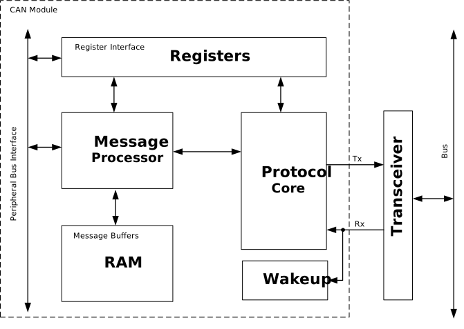
CAN Controller Block Diagram
Protocol Core: Executes the complete CAN underlying protocol logic, including bit timing control, frame parsing and assembly, clock division, and sampling mechanisms. The Protocol Core interacts with the Message Processor via a dedicated data and control interface to perform actual message transmission and reception.
Message Processor: Manages message scheduling and storage. It arbitrates RAM access between the APB bus and the Protocol Core to ensure data consistency. In the receive direction, it scans RAM to allocate storage space for incoming messages. In the transmit direction, it determines the next message to be transmitted based on priority. Additionally, the Message Processor supports hardware auto-reply or storage for remote frames.
Message Buffers: Dedicated internal SRAM space, managed by the Message Processor, used to buffer and store messages pending transmission and already received. Each CAN module contains 16 independently configurable message buffers.
Wakeup Circuit: Handles bus wakeup functionality. In low-power mode, it continuously monitors the Rx pin. Once a dominant (low) level is detected for a duration exceeding the predefined threshold, it triggers a wakeup signal to restore the CAN module and the entire system to the active state.
Register Interface: Allows the CPU to access the internal control and status registers of the CAN module for configuration, status querying, and interrupt management.
Transceiver: Typically located external to the controller, it converts the logic levels output by the Protocol Core into differential signals required by the physical bus, and converts bus differential signals back into logic levels for the controller to read.
Function Description
Protocol Frame Formats
According to the ISO 11898-1 standard, CAN supports four frame types: Data Frame, Remote Frame, Error Frame, and Overload Frame. Additionally, the Inter-Frame Space separates consecutive frames.
Data Frame
Data frames carry data payloads between nodes and are the most common frame type. CAN supports standard data frames (11-bit identifier) and extended data frames (29-bit identifier).
Standard Data Frame: Uses an 11-bit identifier (Base ID), with a maximum payload of 8 bytes.

Standard Data Frame
Extended Data Frame: Uses a 29-bit identifier (Extended ID), distinguished from standard frames by the IDE bit.

Extended Data Frame
A data frame consists of the following functional segments in sequential order:
Start of Frame (SOF): A single dominant bit marking the beginning of the frame, used for hard synchronization.
Arbitration Field: Contains the identifier (ID), RTR, IDE, and SRR bits. The ID determines the message priority; a lower numerical value indicates a higher priority.
Control Field: Contains the Data Length Code (DLC, 4 bits) and reserved bits. The DLC specifies the number of bytes in the data field (0 to 8).
Data Field: The payload, ranging from 0 to 8 bytes, transmitted MSB first.
CRC Field: Contains a 15-bit CRC sequence and a 1-bit recessive CRC delimiter, computed automatically by hardware.
ACK Field: The transmitter outputs a recessive bit; any node that has successfully received the frame responds with a dominant bit.
End of Frame (EOF): 7 consecutive recessive bits marking the end of the frame.
Remote Frame
Remote frames are used to request a specific node to transmit data. Their structure is similar to that of a data frame, but the RTR bit is recessive and there is no data field. Remote frames support both standard and extended formats.

Standard Remote Frame

Extended Remote Frame
Error Frame
An error frame is transmitted when a node detects a bus error to disrupt the current communication and notify other nodes. It consists of an error flag (6 bits) and an error delimiter (8 recessive bits). There are two types:
Active Error Flag: Transmitted by an error-active node, consisting of 6 consecutive dominant bits.
Passive Error Flag: Transmitted by an error-passive node, consisting of 6 consecutive recessive bits.
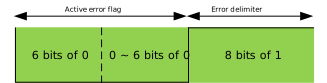
Active Error Frame
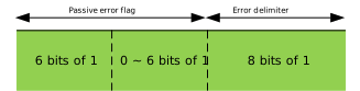
Passive Error Frame
Overload Frame
An overload frame is used to request additional inter-frame delay. Its structure is similar to an active error frame, consisting of an overload flag (6 consecutive dominant bits) and an overload delimiter (8 recessive bits).
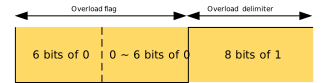
Overload Frame
Inter-Frame Space
The ISO 11898-1 standard defines the Inter-Frame Space, which separates a data frame or remote frame from any preceding frame. The Inter-Frame Space consists of the following phases:
Intermission: 3 consecutive recessive bits. During this period, no node is permitted to initiate a transmission.
Suspend: An error-passive node must wait an additional 8 recessive bit times after the intermission before participating in the next bus arbitration. Error-active nodes are not subject to this restriction.
Bus Idle: If no data transmission occurs after the intermission and suspend times have elapsed, the bus enters the idle state, at which point any node may initiate the next transmission.
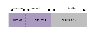
Inter-Frame Space
Note
No inter-frame space is inserted before an error frame or an overload frame.
Clock Domains
Each CAN module has two clock domains: core_clk for primary CAN functions, and a low-frequency clock (OSC4M) for the wakeup circuit. The core_clk clock domain structure is shown below:
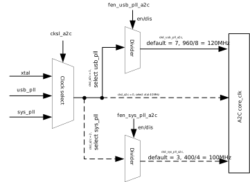
Clock Source Selection
core_clk provides three selectable clock sources:
XTAL 40 MHz
USB PLL
SYS PLL
The clock source is selected via the cksl_can field in REG_LSYS_CKSL_GRP0: cksl_can = 0 selects XTAL (40 MHz), cksl_can = 1 selects USB PLL (default), and cksl_can = 3 selects SYS PLL.
If XTAL is selected (
cksl_can = 0), the 40 MHz crystal oscillator clock is used directly ascore_clk.If a PLL is selected (USB PLL or SYS PLL), two additional parameters must be configured:
Clock enable (e.g.,
fen_usb_pll_canin REG_LSYS_CKD_FEN_USB_PLL)Clock divider (e.g.,
ckd_usb_pll_canin REG_LSYS_CKD_USB_PLL_GRP0).
Bit Timing and Baud Rate
The chip provides two CAN modules. Bit timing parameters can be configured individually for each CAN node, supporting communication rates of up to 1 Mbit/s.
Bit Timing Decomposition
According to ISO 11898-1, a bit time is divided into four segments: Synchronization Segment (Sync_Seg), Propagation Segment (Prop_Seg), Phase Buffer Segment 1 (Phase_Seg1), and Phase Buffer Segment 2 (Phase_Seg2):
Sync_Seg: Fixed at 1 Tq. This is the expected position for bit level transitions, used to synchronize all nodes on the bus.
Prop_Seg: Compensates for signal propagation delay on the physical bus and internal hardware delay of the transceiver.
Phase_Seg1: A buffer segment before the sample point, which can be temporarily lengthened during resynchronization.
Phase_Seg2: A buffer segment after the sample point, which can be temporarily shortened during resynchronization.
A Time Quantum (Tq) is the minimum time unit in bit timing configuration. The length of all time segments is specified in units of Tq. The Tq duration is derived from core_clk divided by the Baud Rate Prescaler (BRP):
Tq = (can_brp + 1) / core_clk
The following figure shows the timing diagram of a complete bit time:
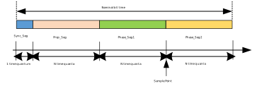
The controller samples the bus level at the boundary between Phase_Seg1 and Phase_Seg2 (the sample point). By adjusting the length of each segment, the sample point position within the bit time can be controlled. A complete bit time typically consists of 8 to 25 Tq. The Tq allocation rules for each segment are as follows:
Parameter |
Range |
Description |
|---|---|---|
Prescaler (BRP) |
1 ~ 32 |
Tq = (can_brp + 1) / core_clk |
Sync_Seg |
1 Tq (Fixed) |
Synchronizes all nodes on the bus |
Prop_Seg |
1 ~ 8 Tq |
Compensates for physical delay times within the network |
Phase_Seg1 |
1 ~ 8 Tq |
Compensates for edge phase errors; can be lengthened during resync |
Phase_Seg2 |
2 ~ 8 Tq |
Compensates for edge phase errors; can be shortened during resync |
SJW (Sync Jump Width) |
1 ~ 4 Tq |
May not exceed the lesser of Phase_Seg1 and Phase_Seg2 |
Bit Timing Register Configuration
Bit timing parameters are programmed via the CAN_BIT_TIMING register. To simplify configuration, the controller merges Prop_Seg and Phase_Seg1 into can_tseg1, while Phase_Seg2 corresponds to can_tseg2. Note that can_brp, can_tseg1, and can_tseg2 are 0-based register fields — the hardware internally adds 1 to obtain the actual divider or segment length. The register field mapping is as follows:
can_brp: Prescaler. Actual divider =can_brp + 1;Tq = (can_brp + 1) / core_clk.can_tseg1: Merged segment (Prop_Seg + Phase_Seg1). Actual length =can_tseg1 + 1; register value =Prop_Seg + Phase_Seg1 - 1.can_tseg2: Phase_Seg2. Actual length =can_tseg2 + 1; register value =Phase_Seg2 - 1.can_sjw: Sync Jump Width.can_sjw = SJW(direct mapping, no offset).
The baud rate calculation formula is:
Baud Rate = core_clk / ((can_brp + 1) × (1 + (can_tseg1 + 1) + (can_tseg2 + 1)))
For example, with core_clk = 40 MHz, can_brp = 1, can_tseg1 = 14, and can_tseg2 = 3, the baud rate is 1 Mbit/s:
Baud Rate = 40 / ((1 + 1) × (1 + (14 + 1) + (3 + 1)))
          = 40 / (2 × 20)
          = 1 Mbit/s
The sample point position within the bit time can be calculated using the following formula:
Sample Point = (1 + can_tseg1 + 1) / (1 + (can_tseg1 + 1) + (can_tseg2 + 1))
In this configuration, the sample point is located at 80% of the bit time.
The following table lists reference configurations for commonly used baud rates with core_clk = 40 MHz:
Baud Rate |
can_brp |
can_tseg1 |
can_tseg2 |
SJW |
Sample Point |
|---|---|---|---|---|---|
1 Mbit/s |
1 |
14 |
3 |
1 |
80% |
500 kbit/s |
3 |
14 |
3 |
1 |
80% |
250 kbit/s |
7 |
14 |
3 |
1 |
80% |
125 kbit/s |
15 |
14 |
3 |
1 |
80% |
Triple Sampling Mode
Setting can_tri_sample in CAN_CTL to 1 enables triple sampling mode. In this mode, the controller samples the input signal three times near the sample point, with each sample separated by 1 Tq. The final logic level is determined by a majority vote of the three sampled values. This effectively filters out signal glitches and improves communication robustness.
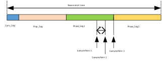
Note
Triple sampling mode is recommended for low bit rates (below 125 kbit/s). At lower rates, each Tq has a longer duration, making the signal more susceptible to external interference. The triple sampling mechanism provides better filtering under such conditions.
Operating Modes
The CAN module supports three operating modes: Normal Mode, Sleep Mode, and Test Mode.
Normal Mode
This is the default operating mode. All submodules (Message Processor, RAM, Protocol Core, and Registers) operate collaboratively to perform message transmission and reception, error handling, and interrupt reporting.
Sleep Mode
In Sleep Mode, most submodules are clock-gated; only the wakeup circuit remains active. The CAN cannot transmit or receive any frames, and both the module and the system enter a low-power state.
Sleep mode is entered by setting can_sleep_en in CAN_SLEEP_MODE to 1. The CAN uses the low-frequency OSC4M clock to drive the wakeup circuit. The system must keep OSC4M active to support wakeup monitoring.
The wakeup circuit operates only in Sleep Mode. It monitors the duration of the dominant level (low level) on the Rx pin and compares it against a predefined threshold:
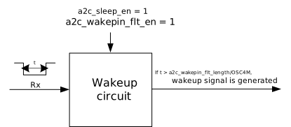
If the low-level duration exceeds the threshold, a wakeup signal is generated to reactivate the CAN module and the entire system.
If the threshold is not exceeded, the module and the system remain in the sleep state.
Warning
Wakeup detection is independent of the protocol frame content. The frame that triggers the wakeup cannot be received by the CAN. Whether subsequent data can be received depends on the sender’s retransmission mechanism.
Before wakeup, ensure that the external transceiver is in its normal operating state rather than standby or sleep mode.
Test Mode
CAN provides two test modes: Silent Mode and Loopback Mode, primarily for node self-testing and bus debugging. To enter test mode, set test_mode_en in CAN_CTL to 1 to enable test functions, then select the specific test mode via can_test_cfg in CAN_TEST.
Silent Mode: Also referred to as Bus Monitoring Mode in the ISO 11898-1 standard. In this mode, the CAN receives all frames on the bus normally but does not transmit any frames (including data and error frames) or ACK bits, and therefore does not affect the bus. This mode is commonly used for analyzing bus communication traffic.
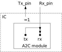
Loopback Mode: Used to verify the internal digital logic of the CAN controller. It is divided into External Loopback and Internal Loopback:
External Loopback: The frame is physically transmitted from the Tx pin onto the bus and can be captured by an external analyzer. The controller receives only frames from its own Tx end, ignoring all other frames on the bus.
Internal Loopback: The frame is looped back entirely within the CAN controller and is not output from the Tx pin to the external bus.
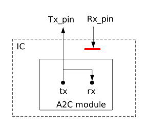
External Loopback Mode
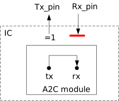
Internal Loopback Mode
Message Processing and Buffer Management
The Message Processor reduces CPU load by taking over storage scheduling for message transmission and reception. It arbitrates RAM access between the CPU (APB bus) and the Protocol Core to ensure data consistency.
Transmit direction: Schedules pending messages for transmission based on priority.
Receive direction: Scans RAM and applies filtering and masking mechanisms to allocate storage space for received messages.
The architectural relationship between RAM, Message Processor, Protocol Core, and Registers is shown below:
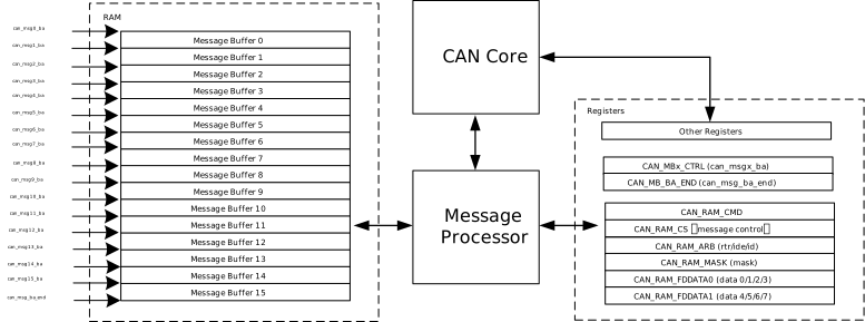
CAN uses registers such as CAN_RAM_ARB, CAN_RAM_MASK, CAN_RAM_CS, CAN_RAM_DATA, and CAN_MB_BA_END to manage message buffers.
Message Buffer Configuration
Each CAN module is equipped with an independent RAM (352 × 32 bits), logically divided into 16 message buffers (MB0 ~ MB15). Each buffer can store only one CAN message, with individually configurable space (default: 6 × 32 bits).
The base address of each buffer is set via can_msgx_ba in CAN_MBx_CTRL (word-aligned), and the valid RAM address range is defined by can_msg_ba_end in CAN_MB_BA_END.
For example, if can_msg0_ba in CAN_MB0_CTRL is 0x0 and can_msg1_ba in CAN_MB1_CTRL is 0x6, MB0 is allocated 6 × 32 bits of storage space.
Receive Filters
The Rx processor uses three types of receive filters for hardware-level message filtering. These filters can be flexibly combined to meet various application requirements.
Identifier (ID) Filter:
can_ram_id(29 bits) in CAN_RAM_ARB defines the expected message ID, andcan_ram_id_mask(29 bits) in CAN_RAM_MASK provides the corresponding mask:A mask bit of 0 means the corresponding bit is not compared (i.e., don’t care; always matches).
A mask bit of 1 means the corresponding bit in the received frame must strictly match
can_ram_id.
Note
The filtering logic depends on the frame type:
Standard frames (11-bit Base ID): only bits [28:18] of
can_ram_idare compared.Extended frames (29-bit Extended ID): the full range of
can_ram_idbits [28:0] is compared.
For example, when receiving standard frames, if bits [28:18] of CAN_RAM_ARB are set to 0x1 and bits [28:18] of CAN_RAM_MASK are set to 0x7FC (the lowest two mask bits are 0), frames with Base IDs 0x00 through 0x03 will all be received.
Identifier Extension (IDE) Filter:
can_ram_idein CAN_RAM_ARB andcan_ram_ide_maskin CAN_RAM_MASK control frame format filtering:can_ram_ide_mask = 0: Frame format is not distinguished; both standard and extended frames are received.can_ram_ide_mask = 1: Only frames whose IDE bit matchescan_ram_ideare received.
can_ram_ide = 0andcan_ram_ide_mask = 1: Only standard frames are received.can_ram_ide = 1andcan_ram_ide_mask = 1: Only extended frames are received.
Remote Transmission Request (RTR) Filter:
can_ram_rtr_maskin CAN_RAM_MASK controls frame type filtering:can_ram_rtr_mask = 0: Frame type is not distinguished; both data and remote frames are received.can_ram_rtr_mask = 1: Only frames whose RTR bit matchescan_ram_rtrin CAN_RAM_ARB are received.
Message Transmission and Reception Flow
Transmission Flow: The Message Processor continuously scans all buffers in RAM to determine if there are messages pending for transmission, and decides the transmission order based on priority. When the bus is in an intermission, idle, or safe state, the selected message is transferred to the Protocol Core for physical transmission. The CPU configuration steps are as follows:
Fill in the transmission parameters in the RAM interface registers: data (
can_ram_data), ID (can_ram_id), and Data Length Code (can_ram_dlc).Set the RTR bit (
can_ram_rtr) to specify the frame type, and set the IDE bit (can_ram_ide) to indicate the frame format.Set
can_ram_rxtxin CAN_RAM_CS to 1, declaring this buffer for transmission.Write a command to CAN_RAM_CMD to trigger the transfer: set
can_ram_dir = 1(write operation), enablecan_ram_buffer_ento activate the corresponding buffer, then setcan_ram_startto 1 to initiate the hardware transfer. Upon completion,can_ram_startis automatically cleared by hardware.The corresponding
can_msgx_tx_reqin CAN_MBx_STS is set to 1, indicating the message is queued for transmission. Upon successful physical transmission, this bit is cleared andcan_msgx_tx_doneis simultaneously set to 1.
Reception Flow: After a message passes the CRC check, the Message Processor scans all receive buffers, applying filter and mask logic to find a matching buffer. The payload is stored in the corresponding internal RAM location only if the message is received without errors. The CPU configuration steps are as follows:
Write the desired ID (
can_ram_id) and mask (can_ram_id_mask) into the RAM interface registers. For an exact match, all relevant bits in CAN_RAM_MASK should be set to 1.Configure the RTR and IDE bits and their corresponding mask bits as required.
Clear
can_ram_rxtxin CAN_RAM_CS to 0, declaring this buffer for reception.Write a command to CAN_RAM_CMD to commit the configuration.
Once configured, the corresponding
can_msgx_rx_rdyin CAN_MBx_STS is set to 1, indicating hardware readiness. When a new message is successfully matched and received,can_msgx_rx_vldis set to 1, notifying the CPU to read the new data. Simultaneously, the corresponding bit in the global statuscan_rx_doneis asserted, requesting an interrupt to the CPU (if enabled).
Buffer Priority
The CAN controller provides 16 message buffers (MB0 ~ MB15). The priority rules are as follows:
Transmit Priority (Tx): Ascending order by buffer number; a smaller number implies higher priority.
Receive Priority (Rx): Descending order by buffer number; a larger number implies higher matching and storage priority.
This priority mechanism is entirely independent of message content and is automatically managed by hardware.
FIFO Mode
When the FIFO feature is enabled, the first four message buffers (MB12 ~ MB15) are reserved as a hardware FIFO. The Rx FIFO’s filtering conditions (ID, IDE, RTR, and their masks) inherit from the configuration registers of MB12, and the associated Rx interrupts are triggered based on MB12. The FIFO has the highest priority in all Rx matching scheduling.
The logic block diagram of the Rx FIFO is shown below:
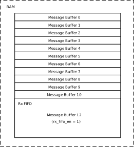
CAN_FIFO_STS is used to monitor FIFO status. The state transitions are as follows:
By default, the FIFO is empty (
fifo_msg_empty = 1).When the FIFO successfully receives the first frame,
fifo_msg_emptychanges to 0, andfifo_msg_lvlincrements to indicate the current FIFO depth.If the FIFO has stored 4 unread frames,
fifo_msg_fullis set to 1. At this point, no overflow has occurred yet (fifo_msg_overflow = 0).If a matching frame continues to be received while the FIFO is full, a rolling overwrite strategy is executed: the earliest received data (originally in MB12) is lost, the data in MB13 shifts to MB12, and so on, with the new message stored in MB15. An overflow error is simultaneously triggered (
fifo_msg_overflow = 1).
DMA Transfer
The CAN module supports receiving data via DMA. DMA can transfer the contents of message buffers (including arbitration field, control field, and data field) to target memory addresses without CPU intervention.
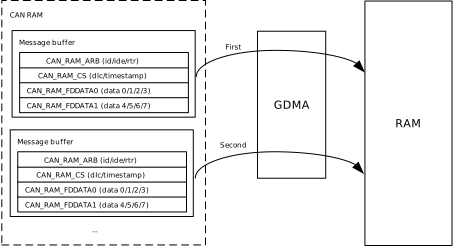
DMA supports two flow control modes: DMA as the flow controller, or CAN as the flow controller. The two modes share identical configuration steps except for the can_rxdma_owner field value in CAN_RXDMA_CFG (0 for DMA, 1 for CAN).
DMA as Flow Controller
When DMA serves as the Flow Controller, the transfer beats are governed by DMA. The configuration steps are as follows:
In CAN_RXDMA_CFG, set
can_rxdma_owner = 0andcan_rxdma_src_msize = 1.In the target message buffer control register CAN_MBx_CTRL, set
can_msgx_rxdma_en = 1to enable the DMA function for that buffer.In CAN_CTL, set
can_rxdma_en = 1to globally enable the DMA function for CAN.Configure the DMA parameters: including source address, destination address, transfer direction, block size, and source burst size (
src_msize). Thesrc_msizein DMA must matchcan_rxdma_src_msizein the CAN register.
CAN as Flow Controller
When CAN acts as the flow controller and actively initiates DMA requests, the configuration steps are as follows:
In CAN_RXDMA_CFG, set
can_rxdma_owner = 1andcan_rxdma_src_msize = 1.In the target message buffer control register CAN_MBx_CTRL, set
can_msgx_rxdma_en = 1to enable the DMA function for that buffer.In CAN_CTL, set
can_rxdma_en = 1to globally enable the DMA function for CAN.Configure the DMA parameters. The
src_msizein DMA must matchcan_rxdma_src_msizeon the CAN side.
Note
Each DMA transfer targets only one message buffer.
The DMA source burst size (
src_msize) must matchcan_rxdma_src_msizeconfigured on the CAN side.
Error Detection and Management
According to the ISO 11898-1 specification, the Error Confinement mechanism detects communication faults on the bus in real-time and restricts severely faulty nodes from causing continuous interference to the bus network through state degradation.
The overall logic block diagram of error confinement is shown below:
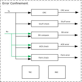
Bit Stuffing
CAN signal synchronization relies on edge transitions. If a large number of consecutive bits of the same polarity appear in the data stream, the receiver cannot maintain synchronization. To address this, the protocol introduces bit stuffing:
Transmitter: When transmitting a data frame or remote frame, for the fields between SOF and the CRC field, upon detecting five consecutive bits of the same polarity, a stuff bit of the opposite polarity is automatically inserted.
Receiver: When receiving a data frame or remote frame, for the fields between SOF and the CRC field, if five consecutive bits of the same polarity are detected, the subsequent opposite-polarity bit is automatically removed. If the 6th bit has the same polarity as the preceding five, a stuff error is flagged.
Fixed-format fields after the CRC field (CRC delimiter, ACK field, and EOF) are not subject to bit stuffing.
Error Types
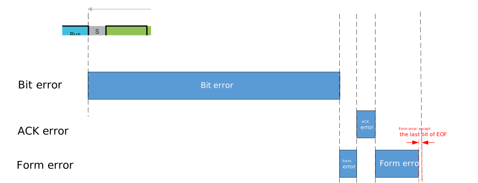
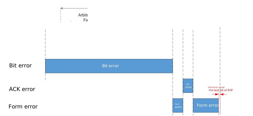
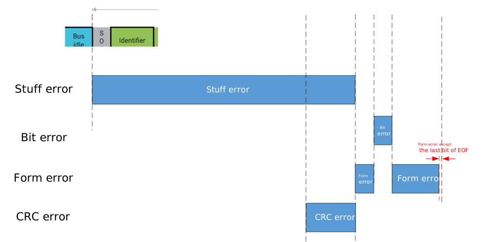
The CAN supports detection of the following five types of hardware protocol errors:
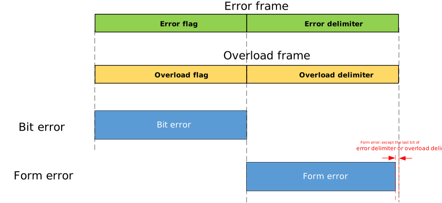
Bit Error: While transmitting a bit, the node monitors (reads back) the actual bus level. If the monitored level differs from the transmitted level (subject to specific exemption rules during the arbitration field or ACK field), a bit error is flagged.
Stuff Error: The node detects six consecutive bits of the same polarity, violating the bit stuffing rule.
CRC Error: The CRC checksum calculated by the receiver does not match the CRC field data in the received frame.
Form Error: A mandatory recessive level is not detected in fixed-format protocol fields (CRC delimiter, ACK delimiter, or EOF).
ACK Error: The transmitting node fails to sample any dominant ACK bit from receiving nodes during the ACK slot.
The following table summarizes the detection scope and error frame transmission timing for each error type:
Error Type |
Error Cause |
Detection Scope |
Error Frame TX Timing |
Detection Unit |
|---|---|---|---|---|
Bit Error |
Transmitted level differs from readback |
Data/Remote Frame (SOF ~ CRC), Error/Overload Frame flags |
Immediately on the next bit |
Transmitter |
Stuff Error |
6 consecutive bits of same polarity |
Data/Remote Frame (SOF ~ CRC sequence) |
Immediately on the next bit |
Receiver |
CRC Error |
CRC checksum mismatch |
Data/Remote Frame (CRC sequence) |
After the ACK delimiter |
Receiver |
Form Error |
Mandatory recessive level not detected in fixed-format field |
Data/Remote Frame (CRC delimiter, ACK delimiter, first 6 bits of EOF), Error/Overload delimiter |
Immediately on the next bit (at the CRC delimiter, treated as CRC error; sent after ACK delimiter) |
Transmitter / Receiver |
ACK Error |
Dominant level not detected in ACK slot |
Data/Remote Frame (ACK slot) |
After the ACK delimiter |
Transmitter |
Note
A bit error is not flagged under the following conditions: during the ID arbitration phase, transmitting a 1 but reading back a 0 is considered arbitration loss; during the ACK slot, if the transmitter outputs a recessive bit and reads back a recessive level, it is not a bit error; during transmission of a passive error flag, reading back a dominant bit is not a bit error.
When a dominant bit is detected on the last bit of the EOF, an overload frame is transmitted instead of an error frame.
Error Detection Scope
According to ISO 11898-1, each error type has a specific detection interval during message transmission and reception.
Error detection scope for a standard data frame during transmission:
Error detection scope for a standard remote frame during transmission:
Error detection scope for an error frame during transmission:
Error detection scope for a standard data frame during reception:
Error detection scope for a standard remote frame during reception:
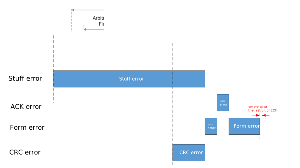
Error detection scope for an error frame during reception:
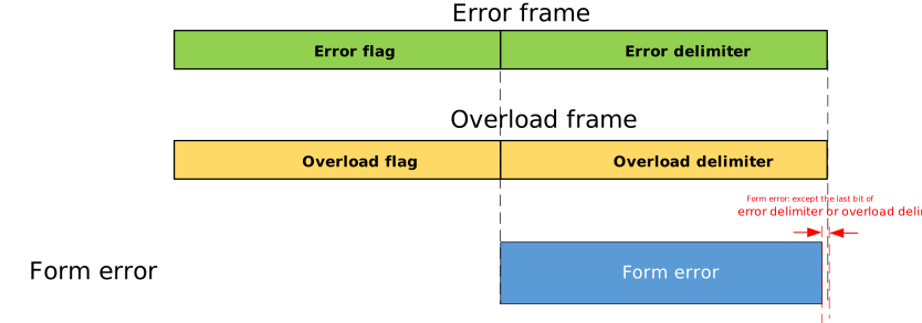
Error States and Counters
The CAN internally maintains two hardware error counters: Transmit Error Counter (TEC) and Receive Error Counter (REC). These counters dynamically increment or decrement according to protocol rules upon errors or successful transmissions/receptions, representing the current health state of the node.
Counter thresholds directly determine the error state of the node. The state transition diagram is shown below:
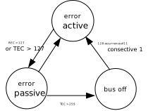
The behavioral characteristics of the three error states are as follows:
Error-Active: TEC ≤ 127 and REC ≤ 127. The node participates normally in bus communication. Upon detecting an error, it immediately transmits an active error flag (6 dominant bits).
Error-Passive: TEC > 127 or REC > 127. The node can still communicate, but upon detecting an error, it transmits only a passive error flag (6 recessive bits), which does not interfere with other nodes. As a transmitter, an additional 8 recessive-bit Suspend period must be inserted between consecutive transmissions.
Bus-Off: TEC > 255. The node is forcibly disconnected from the bus by hardware and cannot transmit or receive any data.
The counting rules for TEC and REC are shown in the following table. Counter changes are triggered at the first bit of the detected error flag. A single message transfer may satisfy multiple conditions simultaneously, and counter values may be adjusted multiple times.
No. |
Trigger Condition |
TEC |
REC |
|---|---|---|---|
1 |
Receiver detects an error (except when the receiver detects a bit error during transmission of an active error flag or overload flag). |
— |
+1 |
2 |
The first bit after the receiver finishes sending an error flag is dominant. |
— |
+8 |
3 |
Transmitter sends an error flag. |
+8 |
— |
4 |
Transmitter detects a bit error during transmission of an active error flag or overload flag. |
+8 |
— |
5 |
Receiver detects a bit error during transmission of an active error flag or overload flag. |
— |
+8 |
6 |
Any node detects excessive consecutive dominant bits after sending an error flag or overload flag:
|
+8 |
+8 |
7 |
Transmitter successfully transmits a frame (ACK received and no errors until the end of EOF). |
If > 0, then -1; if = 0, unchanged |
— |
8 |
Receiver successfully receives a frame (no errors before the ACK slot and dominant ACK bit successfully sent). |
— |
If 1 ≤ REC ≤ 127, then -1; if = 0, unchanged; if > 127, set to 119 ~ 127 |
9 |
Bus-Off recovery (128 × 11 consecutive recessive bits detected) |
Set to 0 |
Set to 0 |
Note
The third item has an exception(TEC unchanged):
The transmitter is error-passive, the ACK error occurs because no dominant bit is detected in the ACK slot, and no dominant bit is detected during transmission of the passive error flag.
The transmitter sends an error flag due to a stuff error during arbitration (unless the violating bit should have been recessive but was monitored as dominant, in which case TEC still increments by 8).
Bus-Off and Recovery
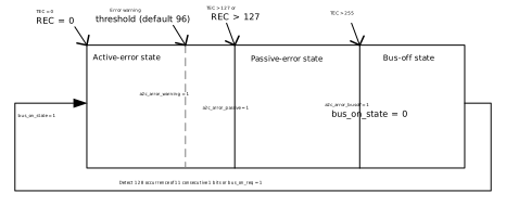
When TEC exceeds 255, the controller enters the Bus-Off state, and the node cannot transmit or receive any data.
The recovery condition is as follows: the controller must detect 128 occurrences of 11 consecutive recessive bit sequences (i.e., 128 bus idle cycles) while in the Bus-Off state, and only after software actively initiates a recovery request (write CAN_BIT_BUS_ON_REQ of CAN_CTL) will the hardware execute the recovery sequence to switch the node back to the error-active state. The current state can be polled via bus_on_state in CAN_STS.
The Bus-Off and recovery mechanism is shown below:
Registers
Base Address:
CAN0_REG : 0x41005000
CAN1_REG : 0x41006000
Name |
Address offset |
Access |
Description |
|---|---|---|---|
000h |
R/W |
Controls the fundamental operations and modes of the CAN bus |
|
004h |
R |
Indicates the overall operational state of the bus |
|
008h |
R |
Monitors the status of the RX FIFO |
|
00Ch |
R/W |
Configures the standard CAN 2.0 bit timing parameters (BRP, SJW, TSEG1, TSEG2) |
|
018h |
R/W |
A global switch to enable or mask various CAN system interrupts |
|
01Ch |
R/W |
Enables or disables receive (RX) interrupts individually for each of the 16 message buffers. |
|
020h |
R/W |
Enables or disables transmit (TX) interrupts individually for each of the 16 message buffers. |
|
024h |
R/W |
Stores the status flags that indicate which specific event (TX, RX, error, etc.) triggered an interrupt. |
|
028h |
R/W |
Provides detailed diagnostics on the type of bus error that occurred |
|
02Ch |
R/W |
Sets the threshold for error warnings and provides a mechanism to clear the internal transmit/receive error counters. |
|
030h |
R |
Displays the current numeric values of the Transmit Error Count (TEC) and Receive Error Count (REC), as well as node states (Warning, Passive, Bus-off) |
|
034h |
R/W |
Flags which specific message buffer encountered an error during its transmission attempt. |
|
038h |
R/W |
Flags which specific message buffer has successfully completed its transmission. |
|
03Ch |
R/W |
Flags which specific message buffer has successfully received a new message. |
|
040h |
R/W |
Manages the internal counter used to apply timestamps to received/transmitted messages, including its prescaler. |
|
044h |
R/W |
Sets up a timer-based trigger mechanism to schedule message transmissions within a specific time window. |
|
048h |
R/W |
Configures how the RX Direct Memory Access (DMA) operates |
|
04Ch |
R |
Acts as the data port from which the DMA controller reads received message payloads. |
|
050h |
R/W |
Manages low-power sleep states, and configures the digital filter for the wakeup pin. |
|
054h |
R/W |
Enables special diagnostic modes, such as silent mode or internal/external loopback testing |
|
100h |
R |
Indicates the individual readiness, validity, and TX/RX status of a specific message buffer. |
|
104h |
R |
Indicates the individual readiness, validity, and TX/RX status of a specific message buffer. |
|
108h |
R |
Indicates the individual readiness, validity, and TX/RX status of a specific message buffer. |
|
10Ch |
R |
Indicates the individual readiness, validity, and TX/RX status of a specific message buffer. |
|
110h |
R |
Indicates the individual readiness, validity, and TX/RX status of a specific message buffer. |
|
114h |
R |
Indicates the individual readiness, validity, and TX/RX status of a specific message buffer. |
|
118h |
R |
Indicates the individual readiness, validity, and TX/RX status of a specific message buffer. |
|
11Ch |
R |
Indicates the individual readiness, validity, and TX/RX status of a specific message buffer. |
|
120h |
R |
Indicates the individual readiness, validity, and TX/RX status of a specific message buffer. |
|
124h |
R |
Indicates the individual readiness, validity, and TX/RX status of a specific message buffer. |
|
128h |
R |
Indicates the individual readiness, validity, and TX/RX status of a specific message buffer. |
|
12Ch |
R |
Indicates the individual readiness, validity, and TX/RX status of a specific message buffer. |
|
130h |
R |
Indicates the individual readiness, validity, and TX/RX status of a specific message buffer. |
|
134h |
R |
Indicates the individual readiness, validity, and TX/RX status of a specific message buffer. |
|
138h |
R |
Indicates the individual readiness, validity, and TX/RX status of a specific message buffer. |
|
13Ch |
R |
Indicates the individual readiness, validity, and TX/RX status of a specific message buffer. |
|
200h |
R/W |
Configures the starting address in RAM and enables DMA functionality for a specific message buffer. |
|
204h |
R/W |
Configures the starting address in RAM and enables DMA functionality for a specific message buffer. |
|
208h |
R/W |
Configures the starting address in RAM and enables DMA functionality for a specific message buffer. |
|
20Ch |
R/W |
Configures the starting address in RAM and enables DMA functionality for a specific message buffer. |
|
210h |
R/W |
Configures the starting address in RAM and enables DMA functionality for a specific message buffer. |
|
214h |
R/W |
Configures the starting address in RAM and enables DMA functionality for a specific message buffer. |
|
218h |
R/W |
Configures the starting address in RAM and enables DMA functionality for a specific message buffer. |
|
21Ch |
R/W |
Configures the starting address in RAM and enables DMA functionality for a specific message buffer. |
|
220h |
R/W |
Configures the starting address in RAM and enables DMA functionality for a specific message buffer. |
|
224h |
R/W |
Configures the starting address in RAM and enables DMA functionality for a specific message buffer. |
|
228h |
R/W |
Configures the starting address in RAM and enables DMA functionality for a specific message buffer. |
|
22Ch |
R/W |
Configures the starting address in RAM and enables DMA functionality for a specific message buffer. |
|
230h |
R/W |
Configures the starting address in RAM and enables DMA functionality for a specific message buffer. |
|
234h |
R/W |
Configures the starting address in RAM and enables DMA functionality for a specific message buffer. |
|
238h |
R/W |
Configures the starting address in RAM and enables DMA functionality for a specific message buffer. |
|
23Ch |
R/W |
Configures the starting address in RAM and enables DMA functionality for a specific message buffer. |
|
2F0h |
R/W |
Defines the ending boundary address in RAM allocated for message buffers. |
|
300h |
R/W |
Serves as the register interface to read or write the actual data payload (up to 64 bytes) into the RAM. |
|
304h |
R/W |
Serves as the register interface to read or write the actual data payload (up to 64 bytes) into the RAM. |
|
308h |
R/W |
Serves as the register interface to read or write the actual data payload (up to 64 bytes) into the RAM. |
|
30Ch |
R/W |
Serves as the register interface to read or write the actual data payload (up to 64 bytes) into the RAM. |
|
310h |
R/W |
Serves as the register interface to read or write the actual data payload (up to 64 bytes) into the RAM. |
|
314h |
R/W |
Serves as the register interface to read or write the actual data payload (up to 64 bytes) into the RAM. |
|
318h |
R/W |
Serves as the register interface to read or write the actual data payload (up to 64 bytes) into the RAM. |
|
31Ch |
R/W |
Serves as the register interface to read or write the actual data payload (up to 64 bytes) into the RAM. |
|
320h |
R/W |
Serves as the register interface to read or write the actual data payload (up to 64 bytes) into the RAM. |
|
324h |
R/W |
Serves as the register interface to read or write the actual data payload (up to 64 bytes) into the RAM. |
|
328h |
R/W |
Serves as the register interface to read or write the actual data payload (up to 64 bytes) into the RAM. |
|
32Ch |
R/W |
Serves as the register interface to read or write the actual data payload (up to 64 bytes) into the RAM. |
|
330h |
R/W |
Serves as the register interface to read or write the actual data payload (up to 64 bytes) into the RAM. |
|
334h |
R/W |
Serves as the register interface to read or write the actual data payload (up to 64 bytes) into the RAM. |
|
338h |
R/W |
Serves as the register interface to read or write the actual data payload (up to 64 bytes) into the RAM. |
|
33Ch |
R/W |
Serves as the register interface to read or write the actual data payload (up to 64 bytes) into the RAM. |
|
340h |
R/W |
Configures the message identifier (ID), format (IDE), and frame type (RTR) for a message buffer being written to or read from RAM. |
|
344h |
R/W |
Configures the acceptance filter masks, defining which bits of an incoming message ID must match to be accepted into the buffer. |
|
348h |
R/W |
Configures control and status attributes of the message, such as Data Length Code (DLC) and direction (TX/RX). |
|
34Ch |
R/W |
Executes the command to transfer data between the CAN_RAM_* registers and the actual internal SRAM for a specified message buffer. |
|
3F8h |
R/W |
Selects and enables internal hardware signals to be routed to debug pins for hardware troubleshooting. |
|
3FCh |
R/W |
A reserved placeholder register used for hardware alignment or future expansion. |
REG_CAN_CTL
Name: CAN bus control register
Size: 32
Address offset: 000h
Read/write access: R/W
Controls the fundamental operations and modes of the CAN bus
Bit |
Symbol |
Access |
INI |
Description |
|---|---|---|---|---|
31:8 |
RSVD |
R |
- |
Reserved |
7 |
CAN_RXDMA_EN |
R/W |
0x0 |
Rx dma enable |
6 |
RSVD |
R |
- |
Reserved |
5 |
RX_FIFO_EN |
R/W |
0x0 |
Rx fifo function enable |
4 |
TEST_MODE_EN |
R/W |
0x0 |
Test mode enable, for lbk or silent mode use |
3 |
AUTO_RE_TX_EN |
R/W |
0x0 |
Auto re-transmission enabled |
2 |
CAN_TRI_SAMPLE |
R/W |
0x0 |
Triple sample mode |
1 |
BUS_ON_REQ |
R/W |
0x0 |
Request to bus_on |
0 |
CAN_EN |
R/W |
0x0 |
Can enable |
REG_CAN_STS
Name: CAN bus status
Size: 32
Address offset: 004h
Read/write access: R
Indicates the overall operational state of the bus
Bit |
Symbol |
Access |
INI |
Description |
|---|---|---|---|---|
31:1 |
RSVD |
R |
- |
Reserved |
0 |
BUS_ON_STATE |
R |
0x0 |
Bus state
|
REG_CAN_FIFO_STS
Name: CAN bus FIFO status
Size: 32
Address offset: 008h
Read/write access: R
Monitors the status of the RX FIFO
Bit |
Symbol |
Access |
INI |
Description |
|---|---|---|---|---|
31:7 |
RSVD |
R |
- |
Reserved |
6:4 |
FIFO_MSG_LVL |
R |
0x0 |
Rx fifo message level |
3 |
RSVD |
R |
- |
Reserved |
2 |
FIFO_MSG_OVERFLOW |
R |
0x0 |
Rx fifo overflow |
1 |
FIFO_MSG_EMPTY |
R |
0x1 |
Rx fifo empty |
0 |
FIFO_MSG_FULL |
R |
0x0 |
Rx fifo full |
REG_CAN_BIT_TIMING
Name: CAN2.0 bit timing
Size: 32
Address offset: 00Ch
Read/write access: R/W
Configures the standard CAN 2.0 bit timing parameters (BRP, SJW, TSEG1, TSEG2)
Bit |
Symbol |
Access |
INI |
Description |
|---|---|---|---|---|
31:24 |
CAN_BRP |
R/W |
0x0 |
CAN bit timing perscaler = <$bit:can_brp>+1 |
23:19 |
RSVD |
R |
- |
Reserved |
18:16 |
CAN_SJW |
R/W |
0x0 |
SJW length = <$bit:can_sjw> |
15:8 |
CAN_TSEG2 |
R/W |
0x0 |
TSEG2 length = <$bit:can_tseg2+1> |
7:0 |
CAN_TSEG1 |
R/W |
0x0 |
TSEG1 length = <$bit:can_tseg1+1> |
REG_CAN_INT_EN
Name: CAN interrupt control
Size: 32
Address offset: 018h
Read/write access: R/W
A global switch to enable or mask various CAN system interrupts
Bit |
Symbol |
Access |
INI |
Description |
|---|---|---|---|---|
31:22 |
RSVD |
R |
- |
Reserved |
21 |
RAM_MOVE_DONE_INT_MASK |
R/W |
0x0 |
Ram move done interrupt mask
|
20 |
BUSOFF_INT_MASK |
R/W |
0x0 |
Wakeup interrupt mask
|
19 |
WAKEUP_INT_MASK |
R/W |
0x0 |
Wakeup interrupt mask
|
18 |
ERROR_INT_MASK |
R/W |
0x0 |
Error interrupt mask
|
17 |
RX_INT_MASK |
R/W |
0x0 |
Rx interrupt mask
|
16 |
TX_INT_MASK |
R/W |
0x0 |
Tx interrupt mask
|
15:6 |
RSVD |
R |
- |
Reserved |
5 |
RAM_MOVE_DONE_INT_EN |
R/W |
0x0 |
Ram move done interrupt enable |
4 |
BUSOFF_INT_EN |
R/W |
0x0 |
Wakeup interrupt enbale |
3 |
WAKEUP_INT_EN |
R/W |
0x0 |
Wakeup interrupt enbale |
2 |
ERROR_INT_EN |
R/W |
0x0 |
Error interrupt enable |
1 |
RX_INT_EN |
R/W |
0x0 |
Rx interrupt enable |
0 |
TX_INT_EN |
R/W |
0x0 |
Tx interrupt enable |
REG_CAN_MB_RXINT_EN
Name: CAN rx interrupt for message buffers
Size: 32
Address offset: 01Ch
Read/write access: R/W
Enables or disables receive (RX) interrupts individually for each of the 16 message buffers.
Bit |
Symbol |
Access |
INI |
Description |
|---|---|---|---|---|
31:16 |
RSVD |
R |
- |
Reserved |
15:0 |
CAN_MB_RXINT_EN |
R/W |
0x0 |
Rx interrupt enable for each message buffer |
REG_CAN_MB_TXINT_EN
Name: CAN tx interrupt for message buffers
Size: 32
Address offset: 020h
Read/write access: R/W
Enables or disables transmit (TX) interrupts individually for each of the 16 message buffers.
Bit |
Symbol |
Access |
INI |
Description |
|---|---|---|---|---|
31:16 |
RSVD |
R |
- |
Reserved |
15:0 |
CAN_MB_TXINT_EN |
R/W |
0x0 |
Tx interrupt enable for each message buffer |
REG_CAN_INT_FLAG
Name: CAN interrupt flags
Size: 32
Address offset: 024h
Read/write access: R/W
Stores the status flags that indicate which specific event (TX, RX, error, etc.) triggered an
interrupt.
Bit |
Symbol |
Access |
INI |
Description |
|---|---|---|---|---|
31:6 |
RSVD |
R |
- |
Reserved |
5 |
RAM_MOVE_DONE_INT_FLAG |
R/W |
0x0 |
Data move from register to CAN IP internal RAM finished interupt, move from RAM to register done will NOT generate interrupt, write one to clear |
4 |
BUSOFF_INT_FLAG |
R/W |
0x0 |
Busoff interrupt flag, write one to clear |
3 |
WAKEUP_INT_FLAG |
R/W |
0x0 |
Wakeup interrupt flag, write one to clear |
2 |
ERROR_INT_FLAG |
R/W |
0x0 |
Error interrupt flag, write to clear |
1 |
RX_INT_FLAG |
R/W |
0x0 |
Rx interrupt flag, write to clear |
0 |
TX_INT_FLAG |
R/W |
0x0 |
Tx interrupt flag, write to clear |
REG_CAN_ERR_STATUS
Name: CAN error status
Size: 32
Address offset: 028h
Read/write access: R/W
Provides detailed diagnostics on the type of bus error that occurred
Bit |
Symbol |
Access |
INI |
Description |
|---|---|---|---|---|
31:10 |
RSVD |
R |
- |
Reserved |
9 |
CAN_ERROR_RX |
R/W |
0x0 |
Can rx error flag |
8 |
CAN_ERROR_TX |
R/W |
0x0 |
Can tx error flag |
7:6 |
RSVD |
R |
- |
Reserved |
5 |
CAN_ERROR_ACK |
R/W |
0x0 |
Latest error is ack error |
4 |
CAN_ERROR_STUFF |
R/W |
0x0 |
Latest error is stuff error |
3 |
CAN_ERROR_CRC |
R/W |
0x0 |
Latest error is ctc error |
2 |
CAN_ERROR_FORM |
R/W |
0x0 |
Latest error is form error |
1 |
CAN_ERROR_BIT1 |
R/W |
0x0 |
Latest error is bit1 error, tx=1 but rx=0 |
0 |
CAN_ERROR_BIT0 |
R/W |
0x0 |
Latest error is bit0 error, tx=0 but rx=1 |
REG_CAN_ERR_CNT_CTL
Name: CAN bus error counter control
Size: 32
Address offset: 02Ch
Read/write access: R/W
Sets the threshold for error warnings and provides a mechanism to clear the internal
transmit/receive error counters.
Bit |
Symbol |
Access |
INI |
Description |
|---|---|---|---|---|
31:17 |
RSVD |
R |
- |
Reserved |
16:8 |
CAN_ERROR_WARN_TH |
R/W |
0x60 |
Error counter warning threshold, programable, default 96. NOTES: 0~127 is availaible to both TEC and REC, 128~255 is only available to TEC |
7:2 |
RSVD |
R |
- |
Reserved |
1 |
RX_ERR_CNT_CLR |
R/W |
0x0 |
Write 1 to clear can_rec |
0 |
TX_ERR_CNT_CLR |
R/W |
0x0 |
Write 1 to clear can_tec |
REG_CAN_ERR_CNT_STS
Name: CAN bus error counter status
Size: 32
Address offset: 030h
Read/write access: R
Displays the current numeric values of the Transmit Error Count (TEC) and Receive Error Count (REC),
as well as node states (Warning, Passive, Bus-off)
Bit |
Symbol |
Access |
INI |
Description |
|---|---|---|---|---|
31 |
RSVD |
R |
- |
Reserved |
30 |
CAN_ERROR_WARNING |
R |
0x0 |
Error counter arrive at warning threshold |
29 |
CAN_ERROR_BUSOFF |
R |
0x0 |
Error counter arrive at bus off level |
28 |
CAN_ERROR_PASSIVE |
R |
0x0 |
Error counter arrive at error passive level |
27:25 |
RSVD |
R |
- |
Reserved |
24:16 |
CAN_REC |
R |
0x0 |
Receive error count |
15:9 |
RSVD |
R |
- |
Reserved |
8:0 |
CAN_TEC |
R |
0x0 |
Transmit error count |
REG_CAN_TX_ERROR_FLAG
Name: CAN tx error flag for each message buffe
Size: 32
Address offset: 034h
Read/write access: R/W
Flags which specific message buffer encountered an error during its transmission attempt.
Bit |
Symbol |
Access |
INI |
Description |
|---|---|---|---|---|
31:16 |
RSVD |
R |
- |
Reserved |
15:0 |
CAN_TX_ERROR_FLAG |
R/W |
0x0 |
Indicate which message tx buffer have error detected, cpu can write 1 to clear |
REG_CAN_TX_DONE
Name: CAN tx done for message buffers
Size: 32
Address offset: 038h
Read/write access: R/W
Flags which specific message buffer has successfully completed its transmission.
Bit |
Symbol |
Access |
INI |
Description |
|---|---|---|---|---|
31:16 |
RSVD |
R |
- |
Reserved |
15:0 |
CAN_TX_DONE |
R/W |
0x0 |
Tx done for each message buffer |
REG_CAN_RX_DONE
Name: CAN rx done for message buffers
Size: 32
Address offset: 03Ch
Read/write access: R/W
Flags which specific message buffer has successfully received a new message.
Bit |
Symbol |
Access |
INI |
Description |
|---|---|---|---|---|
31:16 |
RSVD |
R |
- |
Reserved |
15:0 |
CAN_RX_DONE |
R/W |
0x0 |
Rx done for each message buffer |
REG_CAN_TIME_STAMP
Name: Timestamp function
Size: 32
Address offset: 040h
Read/write access: R/W
Manages the internal counter used to apply timestamps to received/transmitted messages, including
its prescaler.
Bit |
Symbol |
Access |
INI |
Description |
|---|---|---|---|---|
31 |
CAN_TIME_STAMP_EN |
R/W |
0x0 |
Time stamp function enable and time stamp counter start |
30:24 |
RSVD |
R |
- |
Reserved |
23:16 |
CAN_TIME_STAMP_DIV |
R/W |
0x0 |
Timer stamp conter prescalar |
15:0 |
CAN_TIME_STAMP |
R |
0x0 |
Time stamp counter value, up count |
REG_CAN_MB_TRIGGER
Name: CAN tx trigger by timer configuration
Size: 32
Address offset: 044h
Read/write access: R/W
Sets up a timer-based trigger mechanism to schedule message transmissions within a specific time
window.
Bit |
Symbol |
Access |
INI |
Description |
|---|---|---|---|---|
31:25 |
RSVD |
R |
- |
Reserved |
24 |
TX_TRIGGER_EN |
R/W |
0x0 |
End of message buffer base address in RAM |
23:16 |
TX_TRIGGER_CLOSE_OFFSET |
R/W |
0x0 |
End of trigger time = <$bit:tx_trigger_begin> + <$bit:tx_trigger_close_offset> |
15:0 |
TX_TRIGGER_BEGIN |
R/W |
0x0 |
Start of trigger time |
REG_CAN_RXDMA_CFG
Name: RX dma configuration
Size: 32
Address offset: 048h
Read/write access: R/W
Configures how the RX Direct Memory Access (DMA) operates
Bit |
Symbol |
Access |
INI |
Description |
|---|---|---|---|---|
31:25 |
RSVD |
R |
- |
Reserved |
24 |
CAN_RXDMA_OWNER |
R/W |
0x0 |
Can rxdma owner is :
|
23:18 |
RSVD |
R |
- |
Reserved |
17:16 |
CAN_RXDMA_SRC_MSIZE |
R/W |
0x1 |
Rx dma burst size:
|
15:14 |
RSVD |
R |
- |
Reserved |
13:0 |
CAN_RXDMA_FRAME_SIZE |
R |
0x2 |
Can rx dma data frame size = ceil(<rx_dma_data bytes number>/4 ), for example: rx_dma_data is 9~12 bytes, frame size is 3 |
REG_CAN_RX_DMA_DATA
Name: Register for dma access message buffe
Size: 32
Address offset: 04Ch
Read/write access: R
Acts as the data port from which the DMA controller reads received message payloads.
Bit |
Symbol |
Access |
INI |
Description |
|---|---|---|---|---|
31:0 |
CAN_RX_DMA_DATA |
R |
0x0 |
For DMA read received data |
REG_CAN_SLEEP_MODE
Name: sleep mode request and wakeup pin digital filter
Size: 32
Address offset: 050h
Read/write access: R/W
Manages low-power sleep states, and configures the digital filter for the wakeup pin.
Bit |
Symbol |
Access |
INI |
Description |
|---|---|---|---|---|
31:18 |
RSVD |
R |
- |
Reserved |
17 |
CAN_SLEEP_STATE |
R |
0x0 |
Can is sleep or not
|
16 |
CAN_SLEEP_EN |
R/W |
0x0 |
Can sleep enable
|
15:9 |
RSVD |
R |
- |
Reserved |
8 |
CAN_WAKEPIN_FLT_EN |
R/W |
0x0 |
Wakeup pin digital filter enable |
7:0 |
CAN_WAKEPIN_FLT_LENGTH |
R/W |
0x1 |
Wakeup pin digital filter length |
REG_CAN_TEST
Name: test configuration
Size: 32
Address offset: 054h
Read/write access: R/W
Enables special diagnostic modes, such as silent mode or internal/external loopback testing
Bit |
Symbol |
Access |
INI |
Description |
|---|---|---|---|---|
31:2 |
RSVD |
R |
- |
Reserved |
1:0 |
CAN_TEST_CFG |
R/W |
0x0 |
|
REG_CAN_MB0_STS
Size: 32
Address offset: 100h
Read/write access: R
Indicates the individual readiness, validity, and TX/RX status of a specific message buffer.
Bit |
Symbol |
Access |
INI |
Description |
|---|---|---|---|---|
31:4 |
RSVD |
R |
- |
Reserved |
3 |
CAN_MSG0_RX_VLD |
R |
0x0 |
New message have been received in the message buffer |
2 |
CAN_MSG0_RX_RDY |
R |
0x0 |
The message buffer is ready for receiving a new message |
1 |
CAN_MSG0_TX_DONE |
R |
0x0 |
Tx message in the message buffer finish sending |
0 |
CAN_MSG0_TX_REQ |
R |
0x0 |
Tx message is pending for transmit |
REG_CAN_MB1_STS
Size: 32
Address offset: 104h
Read/write access: R
Indicates the individual readiness, validity, and TX/RX status of a specific message buffer.
Bit |
Symbol |
Access |
INI |
Description |
|---|---|---|---|---|
31:4 |
RSVD |
R |
- |
Reserved |
3 |
CAN_MSG1_RX_VLD |
R |
0x0 |
New message have been received in the message buffer |
2 |
CAN_MSG1_RX_RDY |
R |
0x0 |
The message buffer is ready for receiving a new message |
1 |
CAN_MSG1_TX_DONE |
R |
0x0 |
Tx message in the message buffer finish sending |
0 |
CAN_MSG1_TX_REQ |
R |
0x0 |
Tx message is pending for transmit |
REG_CAN_MB2_STS
Size: 32
Address offset: 108h
Read/write access: R
Indicates the individual readiness, validity, and TX/RX status of a specific message buffer.
Bit |
Symbol |
Access |
INI |
Description |
|---|---|---|---|---|
31:4 |
RSVD |
R |
- |
Reserved |
3 |
CAN_MSG2_RX_VLD |
R |
0x0 |
New message have been received in the message buffer |
2 |
CAN_MSG2_RX_RDY |
R |
0x0 |
The message buffer is ready for receiving a new message |
1 |
CAN_MSG2_TX_DONE |
R |
0x0 |
Tx message in the message buffer finish sending |
0 |
CAN_MSG2_TX_REQ |
R |
0x0 |
Tx message is pending for transmit |
REG_CAN_MB3_STS
Size: 32
Address offset: 10Ch
Read/write access: R
Indicates the individual readiness, validity, and TX/RX status of a specific message buffer.
Bit |
Symbol |
Access |
INI |
Description |
|---|---|---|---|---|
31:4 |
RSVD |
R |
- |
Reserved |
3 |
CAN_MSG3_RX_VLD |
R |
0x0 |
New message have been received in the message buffer |
2 |
CAN_MSG3_RX_RDY |
R |
0x0 |
The message buffer is ready for receiving a new message |
1 |
CAN_MSG3_TX_DONE |
R |
0x0 |
Tx message in the message buffer finish sending |
0 |
CAN_MSG3_TX_REQ |
R |
0x0 |
Tx message is pending for transmit |
REG_CAN_MB4_STS
Size: 32
Address offset: 110h
Read/write access: R
Indicates the individual readiness, validity, and TX/RX status of a specific message buffer.
Bit |
Symbol |
Access |
INI |
Description |
|---|---|---|---|---|
31:4 |
RSVD |
R |
- |
Reserved |
3 |
CAN_MSG4_RX_VLD |
R |
0x0 |
New message have been received in the message buffer |
2 |
CAN_MSG4_RX_RDY |
R |
0x0 |
The message buffer is ready for receiving a new message |
1 |
CAN_MSG4_TX_DONE |
R |
0x0 |
Tx message in the message buffer finish sending |
0 |
CAN_MSG4_TX_REQ |
R |
0x0 |
Tx message is pending for transmit |
REG_CAN_MB5_STS
Size: 32
Address offset: 114h
Read/write access: R
Indicates the individual readiness, validity, and TX/RX status of a specific message buffer.
Bit |
Symbol |
Access |
INI |
Description |
|---|---|---|---|---|
31:4 |
RSVD |
R |
- |
Reserved |
3 |
CAN_MSG5_RX_VLD |
R |
0x0 |
New message have been received in the message buffer |
2 |
CAN_MSG5_RX_RDY |
R |
0x0 |
The message buffer is ready for receiving a new message |
1 |
CAN_MSG5_TX_DONE |
R |
0x0 |
Tx message in the message buffer finish sending |
0 |
CAN_MSG5_TX_REQ |
R |
0x0 |
Tx message is pending for transmit |
REG_CAN_MB6_STS
Size: 32
Address offset: 118h
Read/write access: R
Indicates the individual readiness, validity, and TX/RX status of a specific message buffer.
Bit |
Symbol |
Access |
INI |
Description |
|---|---|---|---|---|
31:4 |
RSVD |
R |
- |
Reserved |
3 |
CAN_MSG6_RX_VLD |
R |
0x0 |
New message have been received in the message buffer |
2 |
CAN_MSG6_RX_RDY |
R |
0x0 |
The message buffer is ready for receiving a new message |
1 |
CAN_MSG6_TX_DONE |
R |
0x0 |
Tx message in the message buffer finish sending |
0 |
CAN_MSG6_TX_REQ |
R |
0x0 |
Tx message is pending for transmit |
REG_CAN_MB7_STS
Size: 32
Address offset: 11Ch
Read/write access: R
Indicates the individual readiness, validity, and TX/RX status of a specific message buffer.
Bit |
Symbol |
Access |
INI |
Description |
|---|---|---|---|---|
31:4 |
RSVD |
R |
- |
Reserved |
3 |
CAN_MSG7_RX_VLD |
R |
0x0 |
New message have been received in the message buffer |
2 |
CAN_MSG7_RX_RDY |
R |
0x0 |
The message buffer is ready for receiving a new message |
1 |
CAN_MSG7_TX_DONE |
R |
0x0 |
Tx message in the message buffer finish sending |
0 |
CAN_MSG7_TX_REQ |
R |
0x0 |
Tx message is pending for transmit |
REG_CAN_MB8_STS
Size: 32
Address offset: 120h
Read/write access: R
Indicates the individual readiness, validity, and TX/RX status of a specific message buffer.
Bit |
Symbol |
Access |
INI |
Description |
|---|---|---|---|---|
31:4 |
RSVD |
R |
- |
Reserved |
3 |
CAN_MSG8_RX_VLD |
R |
0x0 |
New message have been received in the message buffer |
2 |
CAN_MSG8_RX_RDY |
R |
0x0 |
The message buffer is ready for receiving a new message |
1 |
CAN_MSG8_TX_DONE |
R |
0x0 |
Tx message in the message buffer finish sending |
0 |
CAN_MSG8_TX_REQ |
R |
0x0 |
Tx message is pending for transmit |
REG_CAN_MB9_STS
Size: 32
Address offset: 124h
Read/write access: R
Indicates the individual readiness, validity, and TX/RX status of a specific message buffer.
Bit |
Symbol |
Access |
INI |
Description |
|---|---|---|---|---|
31:4 |
RSVD |
R |
- |
Reserved |
3 |
CAN_MSG9_RX_VLD |
R |
0x0 |
New message have been received in the message buffer |
2 |
CAN_MSG9_RX_RDY |
R |
0x0 |
The message buffer is ready for receiving a new message |
1 |
CAN_MSG9_TX_DONE |
R |
0x0 |
Tx message in the message buffer finish sending |
0 |
CAN_MSG9_TX_REQ |
R |
0x0 |
Tx message is pending for transmit |
REG_CAN_MB10_STS
Size: 32
Address offset: 128h
Read/write access: R
Indicates the individual readiness, validity, and TX/RX status of a specific message buffer.
Bit |
Symbol |
Access |
INI |
Description |
|---|---|---|---|---|
31:4 |
RSVD |
R |
- |
Reserved |
3 |
CAN_MSG10_RX_VLD |
R |
0x0 |
New message have been received in the message buffer |
2 |
CAN_MSG10_RX_RDY |
R |
0x0 |
The message buffer is ready for receiving a new message |
1 |
CAN_MSG10_TX_DONE |
R |
0x0 |
Tx message in the message buffer finish sending |
0 |
CAN_MSG10_TX_REQ |
R |
0x0 |
Tx message is pending for transmit |
REG_CAN_MB11_STS
Size: 32
Address offset: 12Ch
Read/write access: R
Indicates the individual readiness, validity, and TX/RX status of a specific message buffer.
Bit |
Symbol |
Access |
INI |
Description |
|---|---|---|---|---|
31:4 |
RSVD |
R |
- |
Reserved |
3 |
CAN_MSG11_RX_VLD |
R |
0x0 |
New message have been received in the message buffer |
2 |
CAN_MSG11_RX_RDY |
R |
0x0 |
The message buffer is ready for receiving a new message |
1 |
CAN_MSG11_TX_DONE |
R |
0x0 |
Tx message in the message buffer finish sending |
0 |
CAN_MSG11_TX_REQ |
R |
0x0 |
Tx message is pending for transmit |
REG_CAN_MB12_STS
Size: 32
Address offset: 130h
Read/write access: R
Indicates the individual readiness, validity, and TX/RX status of a specific message buffer.
Bit |
Symbol |
Access |
INI |
Description |
|---|---|---|---|---|
31:4 |
RSVD |
R |
- |
Reserved |
3 |
CAN_MSG12_RX_VLD |
R |
0x0 |
New message have been received in the message buffer |
2 |
CAN_MSG12_RX_RDY |
R |
0x0 |
The message buffer is ready for receiving a new message |
1 |
CAN_MSG12_TX_DONE |
R |
0x0 |
Tx message in the message buffer finish sending |
0 |
CAN_MSG12_TX_REQ |
R |
0x0 |
Tx message is pending for transmit |
REG_CAN_MB13_STS
Size: 32
Address offset: 134h
Read/write access: R
Indicates the individual readiness, validity, and TX/RX status of a specific message buffer.
Bit |
Symbol |
Access |
INI |
Description |
|---|---|---|---|---|
31:4 |
RSVD |
R |
- |
Reserved |
3 |
CAN_MSG13_RX_VLD |
R |
0x0 |
New message have been received in the message buffer |
2 |
CAN_MSG13_RX_RDY |
R |
0x0 |
The message buffer is ready for receiving a new message |
1 |
CAN_MSG13_TX_DONE |
R |
0x0 |
Tx message in the message buffer finish sending |
0 |
CAN_MSG13_TX_REQ |
R |
0x0 |
Tx message is pending for transmit |
REG_CAN_MB14_STS
Size: 32
Address offset: 138h
Read/write access: R
Indicates the individual readiness, validity, and TX/RX status of a specific message buffer.
Bit |
Symbol |
Access |
INI |
Description |
|---|---|---|---|---|
31:4 |
RSVD |
R |
- |
Reserved |
3 |
CAN_MSG14_RX_VLD |
R |
0x0 |
New message have been received in the message buffer |
2 |
CAN_MSG14_RX_RDY |
R |
0x0 |
The message buffer is ready for receiving a new message |
1 |
CAN_MSG14_TX_DONE |
R |
0x0 |
Tx message in the message buffer finish sending |
0 |
CAN_MSG14_TX_REQ |
R |
0x0 |
Tx message is pending for transmit |
REG_CAN_MB15_STS
Size: 32
Address offset: 13Ch
Read/write access: R
Indicates the individual readiness, validity, and TX/RX status of a specific message buffer.
Bit |
Symbol |
Access |
INI |
Description |
|---|---|---|---|---|
31:4 |
RSVD |
R |
- |
Reserved |
3 |
CAN_MSG15_RX_VLD |
R |
0x0 |
New message have been received in the message buffer |
2 |
CAN_MSG15_RX_RDY |
R |
0x0 |
The message buffer is ready for receiving a new message |
1 |
CAN_MSG15_TX_DONE |
R |
0x0 |
Tx message in the message buffer finish sending |
0 |
CAN_MSG15_TX_REQ |
R |
0x0 |
Tx message is pending for transmit |
REG_CAN_MB0_CTRL
Size: 32
Address offset: 200h
Read/write access: R/W
Configures the starting address in RAM and enables DMA functionality for a specific message buffer.
Bit |
Symbol |
Access |
INI |
Description |
|---|---|---|---|---|
31:25 |
RSVD |
R |
- |
Reserved |
24 |
CAN_MSG0_RXDMA_EN |
R/W |
0x0 |
Dma enable when the message buffer used as rx |
23:9 |
RSVD |
R |
- |
Reserved |
8:0 |
CAN_MSG0_BA |
R/W |
9’d0 |
Message buffer base address in RAM |
REG_CAN_MB1_CTRL
Size: 32
Address offset: 204h
Read/write access: R/W
Configures the starting address in RAM and enables DMA functionality for a specific message buffer.
Bit |
Symbol |
Access |
INI |
Description |
|---|---|---|---|---|
31:25 |
RSVD |
R |
- |
Reserved |
24 |
CAN_MSG1_RXDMA_EN |
R/W |
0x0 |
Dma enable when the message buffer used as rx |
23:9 |
RSVD |
R |
- |
Reserved |
8:0 |
CAN_MSG1_BA |
R/W |
9’d6 |
Message buffer base address in RAM |
REG_CAN_MB2_CTRL
Size: 32
Address offset: 208h
Read/write access: R/W
Configures the starting address in RAM and enables DMA functionality for a specific message buffer.
Bit |
Symbol |
Access |
INI |
Description |
|---|---|---|---|---|
31:25 |
RSVD |
R |
- |
Reserved |
24 |
CAN_MSG2_RXDMA_EN |
R/W |
0x0 |
Dma enable when the message buffer used as rx |
23:9 |
RSVD |
R |
- |
Reserved |
8:0 |
CAN_MSG2_BA |
R/W |
9’d12 |
Message buffer base address in RAM |
REG_CAN_MB3_CTRL
Size: 32
Address offset: 20Ch
Read/write access: R/W
Configures the starting address in RAM and enables DMA functionality for a specific message buffer.
Bit |
Symbol |
Access |
INI |
Description |
|---|---|---|---|---|
31:25 |
RSVD |
R |
- |
Reserved |
24 |
CAN_MSG3_RXDMA_EN |
R/W |
0x0 |
Dma enable when the message buffer used as rx |
23:9 |
RSVD |
R |
- |
Reserved |
8:0 |
CAN_MSG3_BA |
R/W |
9’d18 |
Message buffer base address in RAM |
REG_CAN_MB4_CTRL
Size: 32
Address offset: 210h
Read/write access: R/W
Configures the starting address in RAM and enables DMA functionality for a specific message buffer.
Bit |
Symbol |
Access |
INI |
Description |
|---|---|---|---|---|
31:25 |
RSVD |
R |
- |
Reserved |
24 |
CAN_MSG4_RXDMA_EN |
R/W |
0x0 |
Dma enable when the message buffer used as rx |
23:9 |
RSVD |
R |
- |
Reserved |
8:0 |
CAN_MSG4_BA |
R/W |
9’d24 |
Message buffer base address in RAM |
REG_CAN_MB5_CTRL
Size: 32
Address offset: 214h
Read/write access: R/W
Configures the starting address in RAM and enables DMA functionality for a specific message buffer.
Bit |
Symbol |
Access |
INI |
Description |
|---|---|---|---|---|
31:25 |
RSVD |
R |
- |
Reserved |
24 |
CAN_MSG5_RXDMA_EN |
R/W |
0x0 |
Dma enable when the message buffer used as rx |
23:9 |
RSVD |
R |
- |
Reserved |
8:0 |
CAN_MSG5_BA |
R/W |
9’d30 |
Message buffer base address in RAM |
REG_CAN_MB6_CTRL
Size: 32
Address offset: 218h
Read/write access: R/W
Configures the starting address in RAM and enables DMA functionality for a specific message buffer.
Bit |
Symbol |
Access |
INI |
Description |
|---|---|---|---|---|
31:25 |
RSVD |
R |
- |
Reserved |
24 |
CAN_MSG6_RXDMA_EN |
R/W |
0x0 |
Dma enable when the message buffer used as rx |
23:9 |
RSVD |
R |
- |
Reserved |
8:0 |
CAN_MSG6_BA |
R/W |
9’d36 |
Message buffer base address in RAM |
REG_CAN_MB7_CTRL
Size: 32
Address offset: 21Ch
Read/write access: R/W
Configures the starting address in RAM and enables DMA functionality for a specific message buffer.
Bit |
Symbol |
Access |
INI |
Description |
|---|---|---|---|---|
31:25 |
RSVD |
R |
- |
Reserved |
24 |
CAN_MSG7_RXDMA_EN |
R/W |
0x0 |
Dma enable when the message buffer used as rx |
23:9 |
RSVD |
R |
- |
Reserved |
8:0 |
CAN_MSG7_BA |
R/W |
9’d42 |
Message buffer base address in RAM |
REG_CAN_MB8_CTRL
Size: 32
Address offset: 220h
Read/write access: R/W
Configures the starting address in RAM and enables DMA functionality for a specific message buffer.
Bit |
Symbol |
Access |
INI |
Description |
|---|---|---|---|---|
31:25 |
RSVD |
R |
- |
Reserved |
24 |
CAN_MSG8_RXDMA_EN |
R/W |
0x0 |
Dma enable when the message buffer used as rx |
23:9 |
RSVD |
R |
- |
Reserved |
8:0 |
CAN_MSG8_BA |
R/W |
9’d48 |
Message buffer base address in RAM |
REG_CAN_MB9_CTRL
Size: 32
Address offset: 224h
Read/write access: R/W
Configures the starting address in RAM and enables DMA functionality for a specific message buffer.
Bit |
Symbol |
Access |
INI |
Description |
|---|---|---|---|---|
31:25 |
RSVD |
R |
- |
Reserved |
24 |
CAN_MSG9_RXDMA_EN |
R/W |
0x0 |
Dma enable when the message buffer used as rx |
23:9 |
RSVD |
R |
- |
Reserved |
8:0 |
CAN_MSG9_BA |
R/W |
9’d54 |
Message buffer base address in RAM |
REG_CAN_MB10_CTRL
Size: 32
Address offset: 228h
Read/write access: R/W
Configures the starting address in RAM and enables DMA functionality for a specific message buffer.
Bit |
Symbol |
Access |
INI |
Description |
|---|---|---|---|---|
31:25 |
RSVD |
R |
- |
Reserved |
24 |
CAN_MSG10_RXDMA_EN |
R/W |
0x0 |
Dma enable when the message buffer used as rx |
23:9 |
RSVD |
R |
- |
Reserved |
8:0 |
CAN_MSG10_BA |
R/W |
9’d60 |
Message buffer base address in RAM |
REG_CAN_MB11_CTRL
Size: 32
Address offset: 22Ch
Read/write access: R/W
Configures the starting address in RAM and enables DMA functionality for a specific message buffer.
Bit |
Symbol |
Access |
INI |
Description |
|---|---|---|---|---|
31:25 |
RSVD |
R |
- |
Reserved |
24 |
CAN_MSG11_RXDMA_EN |
R/W |
0x0 |
Dma enable when the message buffer used as rx |
23:9 |
RSVD |
R |
- |
Reserved |
8:0 |
CAN_MSG11_BA |
R/W |
9’d66 |
Message buffer base address in RAM |
REG_CAN_MB12_CTRL
Size: 32
Address offset: 230h
Read/write access: R/W
Configures the starting address in RAM and enables DMA functionality for a specific message buffer.
Bit |
Symbol |
Access |
INI |
Description |
|---|---|---|---|---|
31:25 |
RSVD |
R |
- |
Reserved |
24 |
CAN_MSG12_RXDMA_EN |
R/W |
0x0 |
Dma enable when the message buffer used as rx |
23:9 |
RSVD |
R |
- |
Reserved |
8:0 |
CAN_MSG12_BA |
R/W |
9’d72 |
Message buffer base address in RAM |
REG_CAN_MB13_CTRL
Size: 32
Address offset: 234h
Read/write access: R/W
Configures the starting address in RAM and enables DMA functionality for a specific message buffer.
Bit |
Symbol |
Access |
INI |
Description |
|---|---|---|---|---|
31:25 |
RSVD |
R |
- |
Reserved |
24 |
CAN_MSG13_RXDMA_EN |
R/W |
0x0 |
Dma enable when the message buffer used as rx |
23:9 |
RSVD |
R |
- |
Reserved |
8:0 |
CAN_MSG13_BA |
R/W |
9’d78 |
Message buffer base address in RAM |
REG_CAN_MB14_CTRL
Size: 32
Address offset: 238h
Read/write access: R/W
Configures the starting address in RAM and enables DMA functionality for a specific message buffer.
Bit |
Symbol |
Access |
INI |
Description |
|---|---|---|---|---|
31:25 |
RSVD |
R |
- |
Reserved |
24 |
CAN_MSG14_RXDMA_EN |
R/W |
0x0 |
Dma enable when the message buffer used as rx |
23:9 |
RSVD |
R |
- |
Reserved |
8:0 |
CAN_MSG14_BA |
R/W |
9’d84 |
Message buffer base address in RAM |
REG_CAN_MB15_CTRL
Size: 32
Address offset: 23Ch
Read/write access: R/W
Configures the starting address in RAM and enables DMA functionality for a specific message buffer.
Bit |
Symbol |
Access |
INI |
Description |
|---|---|---|---|---|
31:25 |
RSVD |
R |
- |
Reserved |
24 |
CAN_MSG15_RXDMA_EN |
R/W |
0x0 |
Dma enable when the message buffer used as rx |
23:9 |
RSVD |
R |
- |
Reserved |
8:0 |
CAN_MSG15_BA |
R/W |
9’d90 |
Message buffer base address in RAM |
REG_CAN_MB_BA_END
Size: 32
Address offset: 2F0h
Read/write access: R/W
Defines the ending boundary address in RAM allocated for message buffers.
Bit |
Symbol |
Access |
INI |
Description |
|---|---|---|---|---|
31:10 |
RSVD |
R |
- |
Reserved |
9:0 |
CAN_MSG_BA_END |
R/W |
10’d96 |
End of message buffer base address in RAM |
REG_CAN_RAM_DATA_15
Name: CAN data
Size: 32
Address offset: 300h
Read/write access: R/W
Serves as the register interface to read or write the actual data payload (up to 64 bytes) into the
RAM.
Bit |
Symbol |
Access |
INI |
Description |
|---|---|---|---|---|
31:24 |
CAN_RAM_DATA_15_3 |
R/W |
0x0 |
Data_byte 4*15+3 |
23:16 |
CAN_RAM_DATA_15_2 |
R/W |
0x0 |
Data_byte 4*15+2 |
15:8 |
CAN_RAM_DATA_15_1 |
R/W |
0x0 |
Data_byte 4*15+1 |
7:0 |
CAN_RAM_DATA_15_0 |
R/W |
0x0 |
Data_byte 4*15+0 |
REG_CAN_RAM_DATA_14
Name: CAN data
Size: 32
Address offset: 304h
Read/write access: R/W
Serves as the register interface to read or write the actual data payload (up to 64 bytes) into the
RAM.
Bit |
Symbol |
Access |
INI |
Description |
|---|---|---|---|---|
31:24 |
CAN_RAM_DATA_14_3 |
R/W |
0x0 |
Data_byte 4*14+3 |
23:16 |
CAN_RAM_DATA_14_2 |
R/W |
0x0 |
Data_byte 4*14+2 |
15:8 |
CAN_RAM_DATA_14_1 |
R/W |
0x0 |
Data_byte 4*14+1 |
7:0 |
CAN_RAM_DATA_14_0 |
R/W |
0x0 |
Data_byte 4*14+0 |
REG_CAN_RAM_DATA_13
Name: CAN data
Size: 32
Address offset: 308h
Read/write access: R/W
Serves as the register interface to read or write the actual data payload (up to 64 bytes) into the
RAM.
Bit |
Symbol |
Access |
INI |
Description |
|---|---|---|---|---|
31:24 |
CAN_RAM_DATA_13_3 |
R/W |
0x0 |
Data_byte 4*13+3 |
23:16 |
CAN_RAM_DATA_13_2 |
R/W |
0x0 |
Data_byte 4*13+2 |
15:8 |
CAN_RAM_DATA_13_1 |
R/W |
0x0 |
Data_byte 4*13+1 |
7:0 |
CAN_RAM_DATA_13_0 |
R/W |
0x0 |
Data_byte 4*13+0 |
REG_CAN_RAM_DATA_12
Name: CAN data
Size: 32
Address offset: 30Ch
Read/write access: R/W
Serves as the register interface to read or write the actual data payload (up to 64 bytes) into the
RAM.
Bit |
Symbol |
Access |
INI |
Description |
|---|---|---|---|---|
31:24 |
CAN_RAM_DATA_12_3 |
R/W |
0x0 |
Data_byte 4*12+3 |
23:16 |
CAN_RAM_DATA_12_2 |
R/W |
0x0 |
Data_byte 4*12+2 |
15:8 |
CAN_RAM_DATA_12_1 |
R/W |
0x0 |
Data_byte 4*12+1 |
7:0 |
CAN_RAM_DATA_12_0 |
R/W |
0x0 |
Data_byte 4*12+0 |
REG_CAN_RAM_DATA_11
Name: CAN data
Size: 32
Address offset: 310h
Read/write access: R/W
Serves as the register interface to read or write the actual data payload (up to 64 bytes) into the
RAM.
Bit |
Symbol |
Access |
INI |
Description |
|---|---|---|---|---|
31:24 |
CAN_RAM_DATA_11_3 |
R/W |
0x0 |
Data_byte 4*11+3 |
23:16 |
CAN_RAM_DATA_11_2 |
R/W |
0x0 |
Data_byte 4*11+2 |
15:8 |
CAN_RAM_DATA_11_1 |
R/W |
0x0 |
Data_byte 4*11+1 |
7:0 |
CAN_RAM_DATA_11_0 |
R/W |
0x0 |
Data_byte 4*11+0 |
REG_CAN_RAM_DATA_10
Name: CAN data
Size: 32
Address offset: 314h
Read/write access: R/W
Serves as the register interface to read or write the actual data payload (up to 64 bytes) into the
RAM.
Bit |
Symbol |
Access |
INI |
Description |
|---|---|---|---|---|
31:24 |
CAN_RAM_DATA_10_3 |
R/W |
0x0 |
Data_byte 4*10+3 |
23:16 |
CAN_RAM_DATA_10_2 |
R/W |
0x0 |
Data_byte 4*10+2 |
15:8 |
CAN_RAM_DATA_10_1 |
R/W |
0x0 |
Data_byte 4*10+1 |
7:0 |
CAN_RAM_DATA_10_0 |
R/W |
0x0 |
Data_byte 4*10+0 |
REG_CAN_RAM_DATA_9
Name: CAN data
Size: 32
Address offset: 318h
Read/write access: R/W
Serves as the register interface to read or write the actual data payload (up to 64 bytes) into the
RAM.
Bit |
Symbol |
Access |
INI |
Description |
|---|---|---|---|---|
31:24 |
CAN_RAM_DATA_9_3 |
R/W |
0x0 |
Data_byte 4*9+3 |
23:16 |
CAN_RAM_DATA_9_2 |
R/W |
0x0 |
Data_byte 4*9+2 |
15:8 |
CAN_RAM_DATA_9_1 |
R/W |
0x0 |
Data_byte 4*9+1 |
7:0 |
CAN_RAM_DATA_9_0 |
R/W |
0x0 |
Data_byte 4*9+0 |
REG_CAN_RAM_DATA_8
Name: CAN data
Size: 32
Address offset: 31Ch
Read/write access: R/W
Serves as the register interface to read or write the actual data payload (up to 64 bytes) into the
RAM.
Bit |
Symbol |
Access |
INI |
Description |
|---|---|---|---|---|
31:24 |
CAN_RAM_DATA_8_3 |
R/W |
0x0 |
Data_byte 4*8+3 |
23:16 |
CAN_RAM_DATA_8_2 |
R/W |
0x0 |
Data_byte 4*8+2 |
15:8 |
CAN_RAM_DATA_8_1 |
R/W |
0x0 |
Data_byte 4*8+1 |
7:0 |
CAN_RAM_DATA_8_0 |
R/W |
0x0 |
Data_byte 4*8+0 |
REG_CAN_RAM_DATA_7
Name: CAN data
Size: 32
Address offset: 320h
Read/write access: R/W
Serves as the register interface to read or write the actual data payload (up to 64 bytes) into the
RAM.
Bit |
Symbol |
Access |
INI |
Description |
|---|---|---|---|---|
31:24 |
CAN_RAM_DATA_7_3 |
R/W |
0x0 |
Data_byte 4*7+3 |
23:16 |
CAN_RAM_DATA_7_2 |
R/W |
0x0 |
Data_byte 4*7+2 |
15:8 |
CAN_RAM_DATA_7_1 |
R/W |
0x0 |
Data_byte 4*7+1 |
7:0 |
CAN_RAM_DATA_7_0 |
R/W |
0x0 |
Data_byte 4*7+0 |
REG_CAN_RAM_DATA_6
Name: CAN data
Size: 32
Address offset: 324h
Read/write access: R/W
Serves as the register interface to read or write the actual data payload (up to 64 bytes) into the
RAM.
Bit |
Symbol |
Access |
INI |
Description |
|---|---|---|---|---|
31:24 |
CAN_RAM_DATA_6_3 |
R/W |
0x0 |
Data_byte 4*6+3 |
23:16 |
CAN_RAM_DATA_6_2 |
R/W |
0x0 |
Data_byte 4*6+2 |
15:8 |
CAN_RAM_DATA_6_1 |
R/W |
0x0 |
Data_byte 4*6+1 |
7:0 |
CAN_RAM_DATA_6_0 |
R/W |
0x0 |
Data_byte 4*6+0 |
REG_CAN_RAM_DATA_5
Name: CAN data
Size: 32
Address offset: 328h
Read/write access: R/W
Serves as the register interface to read or write the actual data payload (up to 64 bytes) into the
RAM.
Bit |
Symbol |
Access |
INI |
Description |
|---|---|---|---|---|
31:24 |
CAN_RAM_DATA_5_3 |
R/W |
0x0 |
Data_byte 4*5+3 |
23:16 |
CAN_RAM_DATA_5_2 |
R/W |
0x0 |
Data_byte 4*5+2 |
15:8 |
CAN_RAM_DATA_5_1 |
R/W |
0x0 |
Data_byte 4*5+1 |
7:0 |
CAN_RAM_DATA_5_0 |
R/W |
0x0 |
Data_byte 4*5+0 |
REG_CAN_RAM_DATA_4
Name: CAN data
Size: 32
Address offset: 32Ch
Read/write access: R/W
Serves as the register interface to read or write the actual data payload (up to 64 bytes) into the
RAM.
Bit |
Symbol |
Access |
INI |
Description |
|---|---|---|---|---|
31:24 |
CAN_RAM_DATA_4_3 |
R/W |
0x0 |
Data_byte 4*4+3 |
23:16 |
CAN_RAM_DATA_4_2 |
R/W |
0x0 |
Data_byte 4*4+2 |
15:8 |
CAN_RAM_DATA_4_1 |
R/W |
0x0 |
Data_byte 4*4+1 |
7:0 |
CAN_RAM_DATA_4_0 |
R/W |
0x0 |
Data_byte 4*4+0 |
REG_CAN_RAM_DATA_3
Name: CAN data
Size: 32
Address offset: 330h
Read/write access: R/W
Serves as the register interface to read or write the actual data payload (up to 64 bytes) into the
RAM.
Bit |
Symbol |
Access |
INI |
Description |
|---|---|---|---|---|
31:24 |
CAN_RAM_DATA_3_3 |
R/W |
0x0 |
Data_byte 4*3+3 |
23:16 |
CAN_RAM_DATA_3_2 |
R/W |
0x0 |
Data_byte 4*3+2 |
15:8 |
CAN_RAM_DATA_3_1 |
R/W |
0x0 |
Data_byte 4*3+1 |
7:0 |
CAN_RAM_DATA_3_0 |
R/W |
0x0 |
Data_byte 4*3+0 |
REG_CAN_RAM_DATA_2
Name: CAN data
Size: 32
Address offset: 334h
Read/write access: R/W
Serves as the register interface to read or write the actual data payload (up to 64 bytes) into the
RAM.
Bit |
Symbol |
Access |
INI |
Description |
|---|---|---|---|---|
31:24 |
CAN_RAM_DATA_2_3 |
R/W |
0x0 |
Data_byte 4*2+3 |
23:16 |
CAN_RAM_DATA_2_2 |
R/W |
0x0 |
Data_byte 4*2+2 |
15:8 |
CAN_RAM_DATA_2_1 |
R/W |
0x0 |
Data_byte 4*2+1 |
7:0 |
CAN_RAM_DATA_2_0 |
R/W |
0x0 |
Data_byte 4*2+0 |
REG_CAN_RAM_DATA_1
Name: CAN data
Size: 32
Address offset: 338h
Read/write access: R/W
Serves as the register interface to read or write the actual data payload (up to 64 bytes) into the
RAM.
Bit |
Symbol |
Access |
INI |
Description |
|---|---|---|---|---|
31:24 |
CAN_RAM_DATA_1_3 |
R/W |
0x0 |
Data_byte 4*1+3 |
23:16 |
CAN_RAM_DATA_1_2 |
R/W |
0x0 |
Data_byte 4*1+2 |
15:8 |
CAN_RAM_DATA_1_1 |
R/W |
0x0 |
Data_byte 4*1+1 |
7:0 |
CAN_RAM_DATA_1_0 |
R/W |
0x0 |
Data_byte 4*1+0 |
REG_CAN_RAM_DATA_0
Name: CAN data
Size: 32
Address offset: 33Ch
Read/write access: R/W
Serves as the register interface to read or write the actual data payload (up to 64 bytes) into the
RAM.
Bit |
Symbol |
Access |
INI |
Description |
|---|---|---|---|---|
31:24 |
CAN_RAM_DATA_0_3 |
R/W |
0x0 |
Data_byte 4*0+3 |
23:16 |
CAN_RAM_DATA_0_2 |
R/W |
0x0 |
Data_byte 4*0+2 |
15:8 |
CAN_RAM_DATA_0_1 |
R/W |
0x0 |
Data_byte 4*0+1 |
7:0 |
CAN_RAM_DATA_0_0 |
R/W |
0x0 |
Data_byte 4*0+0 |
REG_CAN_RAM_ARB
Name: CAN message buffer arb field configuration
Size: 32
Address offset: 340h
Read/write access: R/W
Configures the message identifier (ID), format (IDE), and frame type (RTR) for a message buffer
being written to or read from RAM.
Bit |
Symbol |
Access |
INI |
Description |
|---|---|---|---|---|
31 |
RSVD |
R |
- |
Reserved |
30 |
CAN_RAM_RTR |
R/W |
0x0 |
Can frame RTR bit, determine DATA or REMOTE frame |
29 |
CAN_RAM_IDE |
R/W |
0x0 |
Can frame IDE bit, determine standard or extend format |
28:0 |
CAN_RAM_ID |
R/W |
0x0 |
Can frame ID, including high 11 bit standard ID and low 18 bit extend ID |
REG_CAN_RAM_MASK
Name: CAN message buffer arb field mask configuration
Size: 32
Address offset: 344h
Read/write access: R/W
Configures the acceptance filter masks, defining which bits of an incoming message ID must match to
be accepted into the buffer.
Bit |
Symbol |
Access |
INI |
Description |
|---|---|---|---|---|
31 |
RSVD |
R |
- |
Reserved |
30 |
CAN_RAM_RTR_MASK |
R/W |
0x0 |
Can frame RTR mask, 0 means don’t care, 1 means the bit should match |
29 |
CAN_RAM_IDE_MASK |
R/W |
0x0 |
Can frame IDE mask, 0 means don’t care, 1 means the bit should match |
28:0 |
CAN_RAM_ID_MASK |
R/W |
0x0 |
Can frame ID mask, 0 means the ID bit in CAN_RAM_ARB don’t care, 1 means the bit should match. |
REG_CAN_RAM_CS
Name: CAN message type control
Size: 32
Address offset: 348h
Read/write access: R/W
Configures control and status attributes of the message, such as Data Length Code (DLC) and
direction (TX/RX).
Bit |
Symbol |
Access |
INI |
Description |
|---|---|---|---|---|
31:16 |
CAN_RAM_TIMESTAMP |
R/W |
0x0 |
The received message time stamp |
15:7 |
RSVD |
R |
- |
Reserved |
6 |
CAN_RAM_AUTOREPLY |
R/W |
0x0 |
Set the message buffer with remote frame auto reply function |
5 |
CAN_RAM_RXTX |
R/W |
0x0 |
Can frame RX or TX, 0 is for RX, 1 is for TX |
4 |
CAN_RAM_LOST |
R/W |
0x0 |
Data have lost in the read buffer, means more than one frame have beed received since last read; only avaliable when rx FIFO is disabled |
3:0 |
CAN_RAM_DLC |
R/W |
0x0 |
Data length |
REG_CAN_RAM_CMD
Name: CAN message buffer access control
Size: 32
Address offset: 34Ch
Read/write access: R/W
Executes the command to transfer data between the CAN_RAM_* registers and the actual internal SRAM
for a specified message buffer.
Bit |
Symbol |
Access |
INI |
Description |
|---|---|---|---|---|
31 |
CAN_RAM_START |
R/W |
0x0 |
Start to exchange data with RAM, the bit will clear automatically after the data change is finshed. |
30 |
CAN_RAM_DIR |
R/W |
0x0 |
0 is for read from RAM to CAN_RAM_* registers, 1 is for write from CAN_RAM_* to RAM |
29 |
CAN_RAM_BUFFER_EN |
R/W |
0x0 |
Enable the can_ram_acc_num specified message buffer for rx/tx |
28:27 |
RSVD |
R |
- |
Reserved |
26 |
CAN_RAM_ACC_DATA15 |
R/W |
0x0 |
Access CAN_RAM_DATA_15 field, the field will exchange with RAM space |
25 |
CAN_RAM_ACC_DATA14 |
R/W |
0x0 |
Access CAN_RAM_DATA_14 field, the field will exchange with RAM space |
24 |
CAN_RAM_ACC_DATA13 |
R/W |
0x0 |
Access CAN_RAM_DATA_13 field, the field will exchange with RAM space |
23 |
CAN_RAM_ACC_DATA12 |
R/W |
0x0 |
Access CAN_RAM_DATA_12 field, the field will exchange with RAM space |
22 |
CAN_RAM_ACC_DATA11 |
R/W |
0x0 |
Access CAN_RAM_DATA_11 field, the field will exchange with RAM space |
21 |
CAN_RAM_ACC_DATA10 |
R/W |
0x0 |
Access CAN_RAM_DATA_10 field, the field will exchange with RAM space |
20 |
CAN_RAM_ACC_DATA9 |
R/W |
0x0 |
Access CAN_RAM_DATA_9 field, the field will exchange with RAM space |
19 |
CAN_RAM_ACC_DATA8 |
R/W |
0x0 |
Access CAN_RAM_DATA_8 field, the field will exchange with RAM space |
18 |
CAN_RAM_ACC_DATA7 |
R/W |
0x0 |
Access CAN_RAM_DATA_7 field, the field will exchange with RAM space |
17 |
CAN_RAM_ACC_DATA6 |
R/W |
0x0 |
Access CAN_RAM_DATA_6 field, the field will exchange with RAM space |
16 |
CAN_RAM_ACC_DATA5 |
R/W |
0x0 |
Access CAN_RAM_DATA_5 field, the field will exchange with RAM space |
15 |
CAN_RAM_ACC_DATA4 |
R/W |
0x0 |
Access CAN_RAM_DATA_4 field, the field will exchange with RAM space |
14 |
CAN_RAM_ACC_DATA3 |
R/W |
0x0 |
Access CAN_RAM_DATA_3 field, the field will exchange with RAM space |
13 |
CAN_RAM_ACC_DATA2 |
R/W |
0x0 |
Access CAN_RAM_DATA_2 field, the field will exchange with RAM space |
12 |
CAN_RAM_ACC_DATA1 |
R/W |
0x0 |
Access CAN_RAM_DATA_1 field, the field will exchange with RAM space |
11 |
CAN_RAM_ACC_DATA0 |
R/W |
0x0 |
Access CAN_RAM_DATA_0 field, the field will exchange with RAM space |
10 |
CAN_RAM_ACC_ARB |
R/W |
0x0 |
Access CAN_RAM_ARB field, the field will exchange with RAM space |
9 |
CAN_RAM_ACC_CS |
R/W |
0x0 |
Access CAN_RAM_CS field, the field will exchange with RAM space |
8 |
CAN_RAM_ACC_MASK |
R/W |
0x0 |
Access CAN_RAM_MASK field, the field will exchange with RAM space |
7:0 |
CAN_RAM_ACC_NUM |
R/W |
0x0 |
Access buffer number |
REG_CAN_DBG_PORT
Name: debug register
Size: 32
Address offset: 3F8h
Read/write access: R/W
Selects and enables internal hardware signals to be routed to debug pins for hardware
troubleshooting.
Bit |
Symbol |
Access |
INI |
Description |
|---|---|---|---|---|
31:9 |
RSVD |
R |
- |
Reserved |
8 |
CAN_DBG_EN |
R/W |
0x0 |
Debug port enable |
7:0 |
CAN_DBG_SEL |
R/W |
0x0 |
Debug port selection |
REG_CAN_DUMMY
Name: dummy register
Size: 32
Address offset: 3FCh
Read/write access: R/W
A reserved placeholder register used for hardware alignment or future expansion.
Bit |
Symbol |
Access |
INI |
Description |
|---|---|---|---|---|
31:0 |
DUMMY |
R/W |
0x0 |
Rsvd for hw |