Dot-Matrix LED Controller
Supported IC[ RTL8721F ]
Introduction
The Dot-Matrix LED driver chips typically communicate with the host controller via synchronous serial interfaces or proprietary protocols, requiring the host to emulate the corresponding protocol for data exchange. Compared to software emulation, a dedicated hardware IP can apply specialized handling within the reset domain, ensuring that display output remains unaffected even when an exception occurs during a display update.
The Dot-Matrix LED Controller is an LEDC driver module that supports a pseudo I2C protocol. It features unidirectional data transmission without requiring slave acknowledgement or address confirmation, and can transfer up to 127 bytes of data in a single transaction.
Features
Two-wire I2C serial interface: SCL and SDA
Start signal and stop signal generation supported
Supported transfer rates: 100 Kbps, 400 Kbps, and 1 Mbps
Pseudo I2C mode:
Maximum transfer size: 127 bytes
Master-only mode
No ACK/NACK signals required
Power and reset characteristics:
Continues operating during software reset, watchdog reset, and system reset
Block Diagram
The block diagram of the Dot-Matrix LED Controller is shown below:
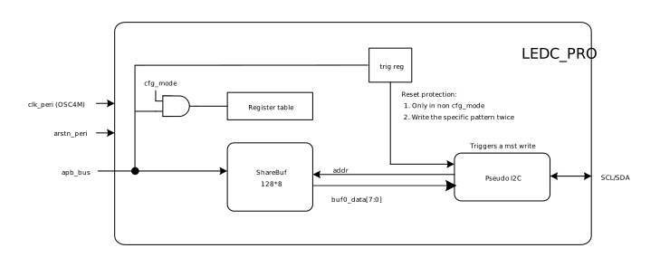
Register Table: stores control parameters and status information
ShareBuf: 128x8-bit shared buffer that caches data to be transferred
Trig Reg: trigger register; writing a specific sequence triggers a pseudo I2C master write operation
Pseudo I2C: pseudo I2C controller that reads data from the shared buffer and generates SCL/SDA signals
OSC4M: module operating clock
Functional Description
Register Protection
The module implements write protection on two critical configuration registers: clock divider LEDC_PRO_R_I2C_CLK_DIV and data length LEDC_PRO_R_I2C_DATA_NUM, preventing accidental writes from altering communication parameters during an ongoing transfer. Before modifying a protected register, software must write 0xa5a5a5a5 to LEDC_PRO_SEQUENCE_CHECK1 (register 0x10[31:0]) to disable protection. After configuration is complete, write 0x00000000 to re-enable protection.
Clock Divider Configuration
During module initialization, software must first perform a software reset on the module (disable and then re-enable the module clock), followed by setting the LEDC_PRO_BIT_R_PSEDO_I2C_EN bit (register 0x08[7]) in the LEDC_PRO_PSDO_I2C_CTL register to enable pseudo I2C mode.
Once enabled, software must disable register protection and set the clock divider factor via LEDC_PRO_R_I2C_CLK_DIV (register 0x08[5:0]). The actual division factor is twice the configured value, with a minimum effective value of 2. After configuration, re-enable register protection.
Timing Control
After software writes the trigger sequence, SDA is pulled low while SCL remains high. The divider counter starts and, after counting LEDC_PRO_R_I2C_CLK_DIV x 2 - 1 clock cycles, SCL is also pulled low. The start signal generation is then complete, and the hardware begins transmitting data bit by bit.
Once all data bytes specified by LEDC_PRO_R_I2C_DATA_NUM have been transferred, the hardware automatically enters the stop phase. SCL is driven high first, and the divider counter continues counting. After counting LEDC_PRO_R_I2C_CLK_DIV x 2 - 1 clock cycles, SDA is also driven high, generating the stop signal.
Transfer Control
Idle State Confirmation
Before initiating each data transfer, software must poll the LEDC_PRO_BIT_R_I2C_TX_STATUS bit (register 0x08[6]) in the LEDC_PRO_PSDO_I2C_CTL register until it reads 1, indicating that the pseudo I2C is in the idle state and subsequent operations may proceed. If this bit reads 0, the previous transfer has not yet completed and software should continue waiting.
Clear RAM Data
After confirming that the module is idle, software must write 1 to the LEDC_PRO_BIT_R_LED_BUF_CLEAR bit (register 0x00[17]) in the LEDC_PRO_LED_PALY_CTL0 register to generate a clear pulse that zeros out any residual data in the RAM, ensuring that the current write is not affected by previous content.
Write Data and Set Transfer Length
Software writes the data to be transmitted into the LEDC_PRO_LED_RAM register. After the data write is complete, software must disable register protection and set the total number of bytes for this transfer via the LEDC_PRO_R_I2C_DATA_NUM field (register 0x08[14:8]) in the LEDC_PRO_PSDO_I2C_CTL register, supporting a maximum of 127 bytes. After configuration, re-enable register protection.
Trigger Hardware Transfer
Once the data is ready, software sequentially writes 0x69696969 and 0x96969696 to the LEDC_PRO_SEQUENCE_CHECK0 register, triggering the hardware to read data from the shared buffer and execute the pseudo I2C transfer. Upon a successful trigger, the LEDC_PRO_BIT_R_SEQ_PASS_FLAG bit (register 0x00[20]) in the LEDC_PRO_LED_PALY_CTL0 register is set to 1. This bit is automatically cleared after software reads it, allowing software to determine that the current transfer has completed and prepare for the next data write.
After the transfer completes, the state machine returns to the idle state, and the LEDC_PRO_BIT_R_I2C_TX_STATUS bit in the LEDC_PRO_PSDO_I2C_CTL register automatically reverts to 1.
Reset Protection
During a software reset, watchdog reset, or system reset, the state of this module and its pad interface is not cleared, ensuring that the display output remains unaffected.
When software needs to actively reset the module, it can do so by disabling and then re-enabling the module clock. The reset operation clears all internal register states and RAM data, so pin mux configuration and module initialization must be performed again after the reset.
Registers
Base Address: 0x4080B200
Name |
Address offset |
Access |
Description |
|---|---|---|---|
000h |
R/W |
||
008h |
R/W |
||
00Ch |
R/W |
||
010h |
R/W |
||
080h |
R/W |
REG_LED_PALY_CTL0
Size: 32
Address offset: 000h
Read/write access: R/W
Bit |
Symbol |
Access |
INI |
Description |
|---|---|---|---|---|
31:21 |
RSVD |
R |
- |
Reserved |
20 |
R_SEQ_PASS_FLAG |
R |
0 |
|
19:18 |
RSVD |
R |
- |
Reserved |
17 |
R_LED_BUF_CLEAR |
R/W |
0 |
Write 1 generate one pulse. Clear and reset ram data |
16:0 |
RSVD |
R |
- |
Reserved |
REG_PSDO_I2C_CTL
Size: 32
Address offset: 008h
Read/write access: R/W
Bit |
Symbol |
Access |
INI |
Description |
|---|---|---|---|---|
31:16 |
RSVD |
R |
- |
Reserved |
15 |
DUMMY |
R/W |
0 |
Dummy |
14:8 |
R_I2C_DATA_NUM |
R/W |
0 |
Psdo i2c data num, unit: byte |
7 |
R_PSEDO_I2C_EN |
R/W |
0 |
Indicate psedo i2c in working, only when this bit=1 can access psedo i2c ram |
6 |
R_I2C_TX_STATUS |
R |
1 |
|
5:0 |
R_I2C_CLK_DIV |
R/W |
0 |
Clock division factor = r_i2c_clk_div * 2, minimum value is 2 |
REG_SEQUENCE_CHECK0
Size: 32
Address offset: 00Ch
Read/write access: R/W
Bit |
Symbol |
Access |
INI |
Description |
|---|---|---|---|---|
31:0 |
R_SEQ_CHK0 |
R/W |
0 |
Sequence check, when this field first write 0x69696969, then write 0x96969696, tirgger led/i2c work |
REG_SEQUENCE_CHECK1
Size: 32
Address offset: 010h
Read/write access: R/W
Bit |
Symbol |
Access |
INI |
Description |
|---|---|---|---|---|
31:0 |
R_SEQ_CHK1 |
R/W |
0 |
Register protect sequence check, when this field = 0xa5a5a5a5, enable access protect register |
REG_LED_RAM
Size: 32
Address offset: 080h
Read/write access: R/W
Bit |
Symbol |
Access |
INI |
Description |
|---|---|---|---|---|
31:0 |
R_LED_RAM_DATA |
R/W |
0 |
Baseaddr+0x80~0xFF 128bytes |