Universal Asynchronous Receiver/Transmitter
Introduction
The Universal Asynchronous Receiver/Transmitter (UART) offers a flexible means of full-duplex data exchange with external equipment that requires an industry-standard NRZ asynchronous serial data format. It offers a very wide range of baud rates using a fractional baud rate generator. Furthermore, numerous optimizations have been implemented for this IP: to address complex interference environments, a debounce function has been incorporated into the receiving path; to enable receiver wake-up in low-power scenarios, a dedicated receiving clock source has been introduced, coupled with an adaptive baud rate drift correction circuit.
Features
UART x 4
Two general UART interfaces: UART0 and UART1
One internal BT UART interface: UART2_BT
One specific UART as LOGUART
UART x 5
Three general UART interfaces: UART0/UART1/UART2
One internal BT UART interface: UART3_BT
One specific UART as LOGUART
UART x 5
Three general UART interfaces: UART0/UART1/UART2
One internal BT UART interface: UART3_BT
One specific UART as LOGUART
UART x 5
Three general UART interfaces: UART0/UART1/UART2
One internal BT UART interface: UART3_BT
One specific UART as LOGUART
UART x 5
Three general UART interfaces: UART0/UART1/UART2
One internal BT UART interface: UART3_BT
One specific UART as LOGUART
UART x 5
Three general UART interfaces: UART0/UART1/UART2
One internal BT UART interface: UART3_BT
One specific UART as LOGUART
UART x 5
Three general UART interfaces: UART0/UART1/UART2
One internal BT UART interface: UART3_BT
One specific UART as LOGUART
UART x 4
Three general UART interfaces: UART0/UART1/UART2
One specific UART as LOGUART
Various UART format: 1 start bit, 7/8 data bits, 0/1 parity bit and 1/2 stop bits
Independent clocks for Tx path and Rx path
Tx path: XTAL 40MHz
Rx path: XTAL 40MHz, OSC 2MHz
Fractional baud rate
Up to 8 Mbps within high-speed mode (XTAL 40MHz)
Up to 115.2 kbps within low-power mode (OSC 2MHz)
Asynchronous Transmit/Receive FIFO
Configurable Auto Flow Control
Interrupt control and error detection
IrDA (SIR mode) encoder and decoder module
Support loopback mode
Low power mode for Rx path
Support Rx path monitor
UART Rx timeout mechanism
DMA interface for DMA transfer
GDMA as DMA Tx/Rx flow controller
UART as DMA Rx flow controller
Operation mode
Polling mode
Interrupt mode
DMA mode
Block Diagram
The block diagram of UART is illustrated below.

The UART consists of several sub-modules, which provide the following functions:
dma_intf
DMA control unit
Interface with GDMA module
tx_fifo
16 x 11-bit entries for UART0/1
32 x 11-bit entries for UART2_BT
rx_fifo
64 x 11-bit entries for UART0/1
32 x 11-bit entries for UART2_BT
tx_fifo
16 x 11-bit entries for UART0/1/2
32 x 11-bit entries for UART3_BT
rx_fifo
64 x 11-bit entries for UART0/1/2
32 x 11-bit entries for UART3_BT
tx_fifo
16 x 11-bit entries for UART0/1/2
32 x 11-bit entries for UART3_BT
rx_fifo
64 x 11-bit entries for UART0/1/2
32 x 11-bit entries for UART3_BT
tx_fifo
16 x 11-bit entries for UART0/1/2
32 x 11-bit entries for UART3_BT
rx_fifo
64 x 11-bit entries for UART0/1/2
32 x 11-bit entries for UART3_BT
tx_fifo
16 x 11-bit entries for UART0/1/2
32 x 11-bit entries for UART3_BT
rx_fifo
64 x 11-bit entries for UART0/1/2
32 x 11-bit entries for UART3_BT
tx_fifo
16 x 11-bit entries for UART0/1/2
32 x 11-bit entries for UART3_BT
rx_fifo
64 x 11-bit entries for UART0/1/2
32 x 11-bit entries for UART3_BT
tx_fifo
16 x 11-bit entries for UART0/1
32 x 11-bit entries for UART2/UART3_BT
rx_fifo
64 x 11-bit entries for UART0/1
32 x 11-bit entries for UART2/UART3_BT
tx_fifo
16 x 11-bit entries for UART0/1
32 x 11-bit entries for UART2
rx_fifo
64 x 11-bit entries for UART0/1
32 x 11-bit entries for UART2
xmitckt
Shift register
Generate UART format data
Support fractional baud rate
irda_sir_encoder
SIR encoder of UART Tx data
recvckt
Receive UART format data
Error detection
Interrupt control
Support fractional baud rate
Oscillator (OSC) clock for low power
Monitor and eliminate Rx baud rate error and own frequency drift
irda_sir_decoder
SIR decoder of UART Rx data
apb_slv_wrap
APB3 bus interface
regmng
Register control unit
Functional Description
This section describes the functional operation of the UART.
UART Serial Protocol
Because the serial communication between the UART and the selected device is asynchronous, additional bits (start bit and stop bit) are added to the serial data to indicate the beginning and end. Utilizing these bits allows two devices to be synchronized. This structure of serial data accompanied by start and stop bits is referred to as a character, as shown below.
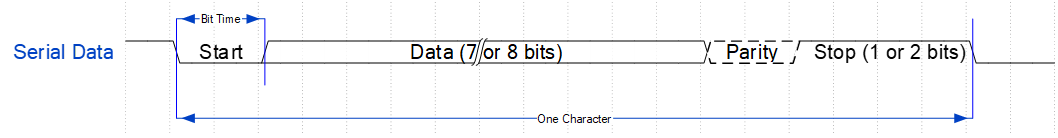
Serial data format
An additional parity bit may be added to the serial character. This bit appears after the last data bit and before the stop bit(s) in the character structure to provide the UART with the ability to perform simple error checking on the received data. The UART Line Control Register (LCR) is used to control the serial character characteristics. The individual bits of the data word (7 or 8 bits) are sent after the start bit, starting with the least-significant bit (LSB). These are followed by the optional parity bit (odd parity, even parity or sticky parity), followed by the stop bit(s), which can be 1 or 2.
Baud Rate Calculation
Baud rate calculation of Tx path and Rx path follows the following equation:

Tx path and Rx path both support fractional baud rate generator. Parameter ovsr[19:0] and ovsr_adj[10:0] are configured depending on IP clock frequency and applied baud rate.
Calculation process of parameter ovsr[19:0] and ovsr_adj[10:0] is shown below, where f represents IP clock frequency.

Total baud rate error shall be less than 3% in order to communicate correctly. Total baud rate error ∆E includes three parts:
∆E = E1 + E2 + E3
Where
E1 is the error of real baud rate of Tx device and expected communication baud rate.
E2 is the frequency drift of Rx IP clock.
E3 is the calculation error of Rx device baud rate (also known as the calculation error between ovsr[19:0] and real baud rate).
For Rx device, E1 and E2 can be both decreased by monitoring baud rate of Rx data, and E3 can be decreased by using fractional baud rate generator.
If maximum sum of E1 and E2 is small (less than 2%), Rx path with XTAL 40MHz clock can be selected, and it can support a higher baud rate.
If maximum sum of E1 and E2 is large (2%~4%), Rx path with OSC 2MHz clock shall be selected, baud rate that it supports is limited, while it can achieve low power by using OSC clock (±3%).
The following table gives the supported frequently-used baud rate of Tx path & Rx path. For Rx path with 2M clock, E3 shall be less than 3%, so minimum value of ovsr[19:0] is 0.5/3%=16, then maximum supported baud rate is 2MHz/16=125000bps, 0.5 is maximum baud rate calculation deviation because there is no fractional part when enabling the Rx monitor baud rate function.
Item |
Tx/Rx path (high-speed mode) |
Rx path (low-power mode) |
|---|---|---|
Clock select |
XTAL 40MHz |
OSC 2MHz (±3%) |
Supported baud rate (bps) |
110, 300, 600, 1200, 2400, 4800, 9600, 14400, 19200, 28800, 38400, 57600, 76800, 115200, 128000, 153600, 230400, 380400, 460800, 500000, 921600, 1000000, 1382400, 1444400, 1500000, 1843200, 2000000, 2100000, 2764800, 3000000, 3250000, 3692300, 3750000, 4000000, 6000000, 8000000 |
110, 300, 600, 1200, 2400, 4800, 9600, 14400, 19200, 28800, 38400, 57600, 76800, 115200 |
The following table lists the error rate of different baud rates when IP clock is XTAL 40MHz, the maximum error rate does not exceed 0.5%.
IP clock |
Theoretical baud rate |
Real baud rate |
Error rate (%) |
|---|---|---|---|
XTAL 40MHz |
110 |
110 |
0 |
XTAL 40MHz |
300 |
300 |
0 |
XTAL 40MHz |
600 |
600 |
0 |
XTAL 40MHz |
1200 |
1200 |
0 |
XTAL 40MHz |
2400 |
2400 |
0 |
XTAL 40MHz |
4800 |
4800 |
0 |
XTAL 40MHz |
9600 |
9600 |
0 |
XTAL 40MHz |
14400 |
14400 |
0 |
XTAL 40MHz |
19200 |
19200 |
0 |
XTAL 40MHz |
28800 |
28800 |
0 |
XTAL 40MHz |
38400 |
38399 |
-0.0026 |
XTAL 40MHz |
57600 |
57604 |
0.0069 |
XTAL 40MHz |
76800 |
76805 |
0.0065 |
XTAL 40MHz |
115200 |
115207 |
0.0061 |
XTAL 40MHz |
128000 |
128000 |
0 |
XTAL 40MHz |
153600 |
153610 |
0.0065 |
XTAL 40MHz |
230400 |
230415 |
0.0065 |
XTAL 40MHz |
380400 |
380228 |
-0.0452 |
XTAL 40MHz |
460800 |
460829 |
0.0063 |
XTAL 40MHz |
500000 |
500000 |
0 |
XTAL 40MHz |
921600 |
921659 |
0.0064 |
XTAL 40MHz |
1000000 |
1000000 |
0 |
XTAL 40MHz |
1382400 |
1384083 |
0.1217 |
XTAL 40MHz |
1444400 |
1444043 |
-0.0247 |
XTAL 40MHz |
1500000 |
1498127 |
-0.1249 |
XTAL 40MHz |
1843200 |
1843318 |
0.0064 |
XTAL 40MHz |
2000000 |
2000000 |
0 |
XTAL 40MHz |
2100000 |
2105263 |
0.2506 |
XTAL 40MHz |
2764800 |
2758621 |
-0.2235 |
XTAL 40MHz |
3000000 |
3007519 |
0.2506 |
XTAL 40MHz |
3250000 |
3252033 |
0.0626 |
XTAL 40MHz |
3692300 |
3703704 |
0.3089 |
XTAL 40MHz |
3750000 |
3738318 |
-0.3115 |
XTAL 40MHz |
4000000 |
4000000 |
0 |
XTAL 40MHz |
6000000 |
5970149 |
-0.4975 |
XTAL 40MHz |
8000000 |
Note
The calculation of error rate retains four decimal places.
IrDA (SIR) Protocol
The Infrared Data Association (IrDA) Serial Infrared (SIR) mode supports bidirectional data communication with remote devices using infrared radiation as the transmission medium. The IrDA 1.0 SIR specification defines a maximum baud rate of 115.2 kbps.
The data format is similar to the standard UART data format. Each data character is transmitted serially, beginning with a start bit, followed by 7 or 8 data bits, and concluding with 1 or 2 stop bits. Parity is not supported in IrDA mode; attempting to enable parity via the Line Control Register (LCR) will result in an incorrect parity bit being inserted into the serial data stream. Once the UART is configured for IrDA support, the IrDA mode can be enabled by setting bit 0 of the MISC Control Register (MISCR).
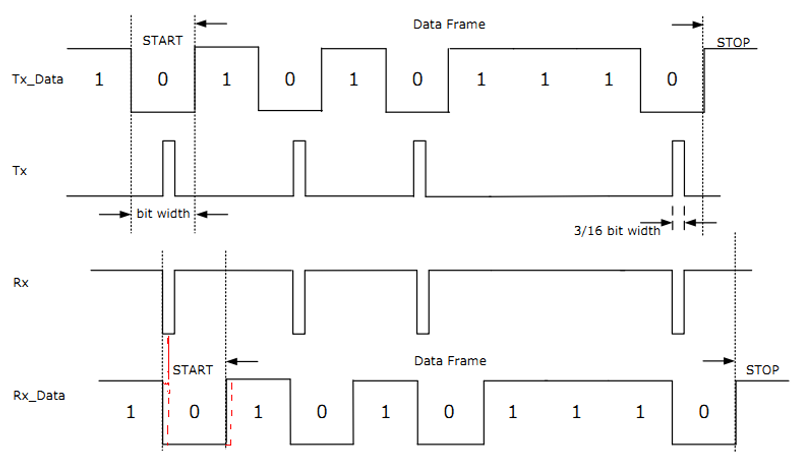
In the IrDA SIR format, transmitting a single infrared pulse indicates a logic 0, whereas the absence of a pulse represents a logic 1. Consequently, each new character begins with an infrared pulse representing the start bit. However, the received data is logically inverted compared to the transmitted data. This inversion occurs because the infrared pulses energize the base of the phototransistor in the IrDA receiver, pulling its output low. This inverted output is subsequently fed to the UART Rx port, restoring the correct UART signal polarity. Additionally, the IrDA input and output logic can be reversed by setting bits 19 and 20 of the MISCR register. The duration of each infrared pulse is nominally 3/16 of a standard serial bit time. The IrDA transmit (Tx) pulse width can also be adjusted via software by configuring the SIR_TX_PWC0 register. The timing diagram below compares the IrDA SIR data format with the standard UART format.
Relationship between IrDA signal and UART signal
The following table details the pulse duration specifications at various signaling rates in Serial Infrared (SIR) mode supported by this chip. The maximum transmission rate is 115.2 kbps.
Signaling rate |
Modulation |
Rate tolerance (%) |
Pulse duration (min.) |
Pulse duration (typ.) |
Pulse duration (max.) |
|---|---|---|---|---|---|
2.4 kbps |
RZI |
±0.87 |
1.41 us |
78.13 us |
88.85 us |
9.6 kbps |
RZI |
±0.87 |
1.41 us |
19.53 us |
22.13 us |
19.2 kbps |
RZI |
±0.87 |
1.41 us |
9.77 us |
11.07 us |
38.4 kbps |
RZI |
±0.87 |
1.41 us |
4.88 us |
5.96 us |
57.6 kbps |
RZI |
±0.87 |
1.41 us |
3.26 us |
4.34 us |
115.2 kbps |
RZI |
±0.87 |
1.41 us |
1.63 us |
2.23 us |
Interrupt
The UART supports both individual and combined interrupt requests, which can both be masked as well. The combined interrupt request is the ORed result of all other UART interrupts after masking. The system designer has the choice of routing individual interrupt requests or only the combined interrupt request to the Interrupt Controller. The UART interrupts are described as follows:
Received Data Available Interrupt (ERBFI) - Set when Rx FIFO Trigger Level is reached or Rx FIFO is full. Rx FIFO Trigger Level can be configured by software in FIFO Control Register (FCR, bit[7:6]), defines the level of receiver FIFO entries at which an interrupt is generated. This interrupt is cleared by hardware when Rx FIFO entries fall below the trigger level. Bit RXFIFO_INT in Line Status Register (LSR, bit8) will be set when this interrupt happens.
Transmitter FIFO Empty Interrupt (ETBEI) - Set when the transmit FIFO is empty. This interrupt is cleared by hardware when data is written into the Tx FIFO buffer. Bit TX_EMPTY in Line Status Register (LSR, bit5) will be set when this interrupt happens.
Receiver Line Status Interrupt (ELSI) - Set when overrun, parity error, framing error or break condition is detected on the Rx line. This interrupt remains set until the Receiver Line Status Interrupt Clear Flag (RLSICF) in Interrupt Clear Register (ICR) is set by the user. Bit OVR_ERR (LSR, bit1), bit PAR_ERR (LSR, bit2), bit FRM_ERR (LSR, bit3) and bit BREAK_INT (LSR, bit4) will be set accordingly when detecting overrun, parity error, framing error and break condition on the Rx line. Bit RXFIFO_ERR (LSR, bit7) will be set when any of the events mentioned before happens. Writing
1to RLSICF will also clear RXFIFO_ERR status.Modem Status Interrupt (EDSSI) - Set when a falling edge is detected on CTS line with hardware auto flow control enabled. This interrupt remains set until the Modem Interrupt Clear Flag (MICF) in ICR is set by the user. Bit MODEM_INT (LSR, bit11) will be set when this interrupt happens.
Rx Path Monitor Done Interrupt (EMDI) - Set when monitor process is over with Rx path monitor function enabled. This interrupt remains set until the Monitor Done Interrupt Clear Flag (MDICF) in ICR is set by the user. Bit MONITOR_DONE_INT (LSR, bit10) will be set when this interrupt happens.
Rx Timeout Interrupt (ETOI) - Set when no character has been input to the Rx FIFO or read from it before time expires when there is at least one character in the Rx FIFO. This interrupt remains set until the Timeout Interrupt Clear Flag (TOICF) in ICR is set by the user. Bit TIMEOUT_INT (LSR, bit9) will be set when this interrupt happens.
RXFIFO Empty Timeout Interrupt (ERETI) - Set when Rx FIFO stays empty until time expires. This interrupt remains set until the RXFIFO Empty Timeout Interrupt Clear Flag (RETICF) in ICR is set by the user. Bit RE_TIMEOUT_INT (LSR, bit13) will be set when this interrupt happens.
Rx Noise Detected Interrupt (ERXNDI) - Set when Rx debouncer has detected noise. This interrupt remains set until the Rx Noise Detected Interrupt Clear Flag (RXNDICF) in ICR is set by the user. Bit RXND_INT (LSR, bit12) will be set when this interrupt happens.
Rx Timeout Interrupt (ETOI) is supported and time can be set in Rx Path Control Register (RX_PATH_CTRL, bit[31:16]).
RXFIFO Empty Timeout Interrupt (ERETI) is not supported.
Rx Timeout Interrupt (ETOI) is supported and time can be set in Rx Path Control Register (RX_PATH_CTRL, bit[31:16]).
RXFIFO Empty Timeout Interrupt (ERETI) is not supported.
Rx Timeout Interrupt (ETOI) is supported and time can be set in Rx Path Control Register (RX_PATH_CTRL, bit[31:16]).
RXFIFO Empty Timeout Interrupt (ERETI) is not supported.
Rx Timeout Interrupt (ETOI) is supported and time can be set in Rx Path Control Register (RX_PATH_CTRL, bit[31:16]).
RXFIFO Empty Timeout Interrupt (ERETI) is not supported.
Rx Timeout Interrupt (ETOI) is supported and time can be set in Rx Path Control Register (RX_PATH_CTRL, bit[31:16]).
RXFIFO Empty Timeout Interrupt (ERETI) is not supported.
Rx Timeout Interrupt (ETOI) is supported and time can be set in Rx Path Control Register (RX_PATH_CTRL, bit[31:16]).
RXFIFO Empty Timeout Interrupt (ERETI) is not supported.
Rx Timeout Interrupt (ETOI) is supported and time can be set in Rx Path Control Register (RX_PATH_CTRL, bit[31:16]).
RXFIFO Empty Timeout Interrupt (ERETI) is supported and time can be set in RXFIFO Empty Interrupt Timeout Threshold Register (TH_RETI, bit[27:0]).
Rx Timeout Interrupt (ETOI) is supported and time can be set in Rx Timeout Threshold Register (RXTO_THRS, bit[27:0]).
RXFIFO Empty Timeout Interrupt (ERETI) is supported and time can be set in Rx Timeout Threshold Register (RXTO_THRS, bit[27:0]).
Auto Flow Control
It is possible to control the serial UART data flow between 2 devices by using the nCTS input and the nRTS output. The following figure shows how to connect the two devices in auto flow control mode.
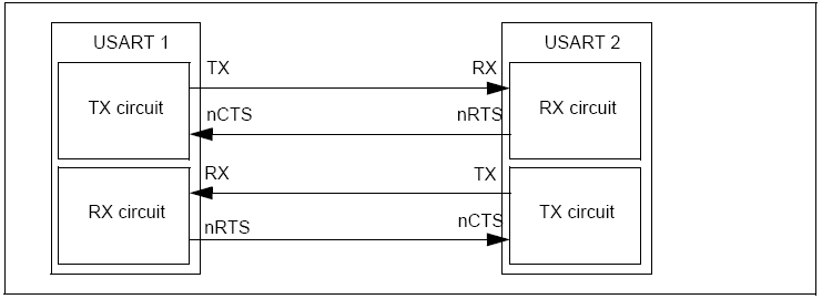
When auto flow control mode is enabled, if input nCTS is deasserted in Tx idle state, the transmission does not occur; if input nCTS is deasserted during transmission, the current transmission is completed before the transmitter stops. When Rx FIFO is almost full, nRTS is deasserted to inform peer device to stop transmission at the end of current transmission.
The UART can be configured to work under hardware data flow control, which is composed of Auto RTS and Auto CTS. Enable Auto Flow Control by asserting AFE bit in the Modem Control Register (MCR, bit5). Auto RTS and Auto CTS are described as follows:
Auto RTS
Auto RTS becomes active when the following occurs:
Auto Flow Control is enabled (MCR[5] is set)
RTS output is enabled (MCR[1] is set)
FIFOs are enabled (FCR[0] is set)
When Auto RTS is enabled (active), RTS signal is forced inactive (high) automatically once the receiver FIFO reaches Rx_FIFO_Trigger_Level.
The optional receiver FIFO threshold values are 1, 1/4, 1/2, and 2 less than full. Since one additional character may be transmitted to the UART after RTS has become inactive as shown in Auto RTS timing (due to data in the other UART has already entered the transmitter block before it recognizes the deassertion of RTS), setting the threshold to 2 less than full makes the best use of the FIFO with a safety zone of one character.
Once the receiver FIFO becomes completely empty by reading the Receiver Buffer Register (RBR_OR_THR), RTS becomes active (low) again, signaling the other UART to continue sending data.
Once the receiver FIFO becomes completely empty by reading the Receiver Buffer Register (RBR_OR_THR), RTS becomes active (low) again, signaling the other UART to continue sending data.
Once the receiver FIFO becomes completely empty by reading the Receiver Buffer Register (RBR_OR_THR), RTS becomes active (low) again, signaling the other UART to continue sending data.
Once the receiver FIFO becomes completely empty by reading the Receiver Buffer Register (RBR_OR_THR), RTS becomes active (low) again, signaling the other UART to continue sending data.
Once the receiver FIFO becomes completely empty by reading the Receiver Buffer Register (RBR_OR_THR), RTS becomes active (low) again, signaling the other UART to continue sending data.
Once the receiver FIFO becomes completely empty by reading the Receiver Buffer Register (RBR_OR_THR), RTS becomes active (low) again, signaling the other UART to continue sending data.
Once the receiver FIFO level falls below (Rx_FIFO_Trigger_Level - 2) by reading the Receiver Buffer Register (RBR_OR_THR), RTS becomes active (low) again, signaling the other UART to continue sending data.
Once the receiver FIFO level falls below (Rx_FIFO_Trigger_Level - 2) by reading the Receiver Buffer Register (RBR_OR_THR), RTS becomes active (low) again, signaling the other UART to continue sending data.
It is important to note that even if everything else is selected and the correct MCR bits are set, if the FIFOs are disabled through FCR bit0, Auto Flow Control is also disabled. When Auto RTS is not implemented or disabled, RTS is controlled solely by MCR bit1. The following figure shows a timing diagram of Auto RTS operation.

Auto RTS timing
Auto CTS
Auto CTS becomes active when the following occurs:
Auto Flow Control is enabled (MCR[5] is set)
FIFOs are enabled (FCR[0] is set)
SIR mode is disabled (MISCR[0] bit is cleared)
When Auto CTS is enabled (active), the UART transmitter is disabled automatically once the CTS input becomes inactive (high). This prevents overflowing the FIFO of the receiving device (e.g. another UART). If the CTS input is not deasserted before the middle of the last stop bit, another character is transmitted before the transmitter is disabled. While the transmitter is disabled, the transmitter FIFO can still be written to, and even overflowed.
The UART status register can be read to check if the transmit FIFO is full (LSR bit6 = 0).
When using the FIFO full status, the software can poll this before each write to the transmitter FIFO. When the CTS input becomes active (low) again, transmission resumes. It is important to note that even if everything else is selected, if the FIFOs are disabled via FCR[0], Auto Flow Control is also disabled. When Auto CTS is not implemented or disabled, the transmitter is unaffected by CTS. A Timing Diagram showing Auto CTS operation can be seen below:

Auto CTS timing
Note
Due to pin count limitations on the SoC, not all UART interfaces support RTS/CTS pins. Please refer to the specific chip datasheet for more pin details. Auto flow control is not supported on UART ports lacking RTS/CTS pins.
DMA Flow Control
The GDMA always acts as the DMA flow controller for UART Tx. However, for UART Rx, either the GDMA or the UART can serve as the DMA flow controller. Note that only the Rx DMA mode is illustrated in this section.
GDMA as DMA flow controller
When the GDMA acts as the DMA flow controller (as shown below), it sets the expected block length before a block transfer begins, and terminates the transfer when the Rx length equals the block length. The rx_dma_req signal is asserted when the data size in the Rx FIFO is greater than or equal to the burst size, and the rx_dma_single signal is asserted when the Rx FIFO is not empty. The rx_dma_ack signal is asserted after the data phase of the last AHB transfer (single or burst) in the current transaction is completed. When the GDMA is the flow controller, the rx_dma_last signal is not sampled and is ignored.
GDMA as DMA flow controller
Specifically, when the data transfer is unpredictable (e.g., the amount of Rx data is unknown), it is recommended to set the GDMA as the flow controller:
The UART Rx burst size and the GDMA burst transaction size should both be set to 1. The GDMA block transfer size should be set to a value larger than the expected amount, or directly to 65535 (the maximum value). Additionally, the RXFIFO Empty Timeout Interrupt (ERETI) should be enabled to notify that the transaction has been halted for a certain period.
Once the RXFIFO Empty Timeout Interrupt (ERETI) is triggered, RXDMA_EN will be cleared automatically by hardware, and a DMA request will not be asserted even if new data enters the Rx FIFO. The number of bytes read from the Rx FIFO by the DMA can be obtained from the register UART_RX_BYTE_CNT. If new data arrives after the interrupt occurs, the user can manually read the remaining data in the Rx FIFO. The user should also disable the DMA.
UART as DMA flow controller
When the UART acts as the DMA flow controller (as shown below), UART asserts the rx_dma_last signal to terminate block transfer when UART has received the whole packet. The finish flag is defined as: no new Rx character arrives within UART_RX_BYTE_CNT time in register UART_RX_PATH_CTRL after the last Rx character.
When the UART acts as the DMA flow controller (as shown below), UART asserts the rx_dma_last signal to terminate block transfer when UART has received the whole packet. The finish flag is defined as: no new Rx character arrives within UART_RX_BYTE_CNT time in register UART_RX_PATH_CTRL after the last Rx character.
When the UART acts as the DMA flow controller (as shown below), UART asserts the rx_dma_last signal to terminate block transfer when UART has received the whole packet. The finish flag is defined as: no new Rx character arrives within UART_RX_BYTE_CNT time in register UART_RX_PATH_CTRL after the last Rx character.
When the UART acts as the DMA flow controller (as shown below), UART asserts the rx_dma_last signal to terminate block transfer when UART has received the whole packet. The finish flag is defined as: no new Rx character arrives within UART_RX_BYTE_CNT time in register UART_RX_PATH_CTRL after the last Rx character.
When the UART acts as the DMA flow controller (as shown below), UART asserts the rx_dma_last signal to terminate block transfer when UART has received the whole packet. The finish flag is defined as: no new Rx character arrives within UART_RX_BYTE_CNT time in register UART_RX_PATH_CTRL after the last Rx character.
When the UART acts as the DMA flow controller (as shown below), UART asserts the rx_dma_last signal to terminate block transfer when UART has received the whole packet. The finish flag is defined as: no new Rx character arrives within UART_RX_BYTE_CNT time in register UART_RX_PATH_CTRL after the last Rx character.
When the UART acts as the DMA flow controller (as shown below), UART asserts the rx_dma_last signal to terminate block transfer when UART has received the whole packet. The finish flag is defined as: no new Rx character arrives within UART_RX_BYTE_CNT time in register UART_RX_PATH_CTRL after the last Rx character.
When the UART acts as the DMA flow controller (as shown below), UART asserts the rx_dma_last signal to terminate block transfer when UART has received the whole packet. The finish flag is defined as: no new Rx character arrives within UART_R_RXTO_THRS time in register UART_RXTO_THRS after the last Rx character, or the total number of bytes received via UART reaches the configured limit of UART_RXDMA_MAX_LEN, which defines the maximum byte count for the reception.
Before rx_dma_req signal is asserted, the amount of data to be transferred is calculated and the following actions will be performed:
If the amount of data to be transferred is less than the DMA Rx burst size, all remaining data will be transferred in a single DMA transaction by asserting rx_dma_single signal. When there is only one byte of data remaining to be transferred, rx_dma_last signal will be asserted and the final byte will be transferred to the destination memory by DMA.
Remaining Rx byte count can be checked in UART_RXDMA_REMAIN_LEN register during transfer. It will be reset to the value of UART_RXDMA_MAX_LEN when DMA transmission is completed (rx_dma_last=1) or rx_dma_en is disabled.

UART as DMA flow controller
The following figure illustrates the DMA interface timing diagram when the total Rx packet length is not a multiple of the burst transaction size. T1 and T2 are burst transfer, T3 and T4 are single transfer. T2 is the last burst transfer of block transfer. After timeout, there are two entries in Rx FIFO, which is less than burst transaction transfer size. Then UART starts two single transfers (T3 and T4) to finish block transfer. rx_dma_last is transferred to GDMA together with the last rx_dma_req. In this case, there may be several single transfers after timeout.

DMA interface timing diagram (block size is not multiple of burst transaction size)
The following figure illustrates the DMA interface timing diagram when the total Rx packet length is a multiple of the burst transaction size. Block transfer is actually done after the last burst transfer of T2. However, UART cannot determine the end of block transfer until timeout happens. In T3, UART starts a dummy single last transfer to inform GDMA, and sets DUMMY_FLAG in the MISCR register for software judgment at the same time. The dummy data can be configured by DUMMY_DATA in MISCR.

DMA interface timing diagram (block size is multiple of burst transaction size)
Low Power Rx
The clock structure of Rx path for UART0, UART1, UART2_BT and LOGUART is similar. The following figure is the clock structure of UARTx Rx path, where x can be from 0 to 2. The cksl_uart signal in REG_CKSL_GRP0 register decides the clock for UARTx Rx path.

In the low-power state:
The OSC2M clock (divided from OSC4M) is supported as the UART Rx clock to wake up the system;
XTAL40M is directly gated. If the XTAL40M clock is used as the UART Rx clock, the system cannot be woken up.
Note
To wake up the system via UART, set PMC_BIT_PST_SLEP_ERCK to 1 to ensure cke_uartx is 1 during sleep.
The clock structure of Rx path for UART0, UART1, UART2, UART3_BT and LOGUART is similar. The following figure is the clock structure of UARTx Rx path, where x can be from 0 to 3. The cksl_uart signal in REG_CKSL_GRP0 register decides the clock for UARTx Rx path.
After the system enters the low-power state, data can be sent to the UART to wake up the system via the UART interrupt.
In the low-power state, XTAL40M/OSC2M clocks can both be selected as the UART Rx clock, allowing the system to be woken up.
Note
If XTAL40M is selected as the clock source, PMC_MASK_PST_SLEP_XMD must be set to 0x3 (normal);
The clock structure of Rx path for UART0, UART1, UART2 and LOGUART is similar. The following figure is the clock structure of UARTx Rx path, where x can be from 0 to 2. The cksl_uart signal and cksl_uart2m signal in REG_CKSL_GRP0 register decide the clock for UARTx Rx path. Rx clock of UART3_BT is always XTAL40M.
After the system enters the low-power state, data can be sent to the UART to wake up the system via the UART interrupt.
In the low-power state, XTAL40M/OSC2M clocks can both be selected as the UART Rx clock, allowing the system to be woken up.
Note
If XTAL40M is selected as the clock source, PMC_MASK_PST_SLEP_XMD must be set to 0x3 (normal);
If OSC2M is selected as the clock source, PMC_BIT_PST_SLEP_ERCK must be set to 1.
The clock structure of Rx path for UART0, UART1, UART2, UART3_BT and LOGUART is similar. The following figure is the clock structure of UARTx Rx path, where x can be from 0 to 3. The cksl_uart signal in REG_CKSL_GRP1 register decides the clock for UARTx Rx path.

After the system enters the low-power state, data can be sent to the UART to wake up the system via the UART interrupt.
In the low-power state, XTAL40M/OSC2M clocks can both be selected as the UART Rx clock, allowing the system to be woken up.
Note
To use XTAL40M as the UART Rx clock, set keep_osc4m_on and sleep_to_08V in ps_config to TRUE in ameba_sleepcfg.c, and set xtal_mode_in_sleep to a proper value (e.g., XTAL_LPS_With_40M).
To use OSC2M as the UART Rx clock, set keep_osc4m_on in ps_config to TRUE in ameba_sleepcfg.c.
The clock structure of Rx path for UART0, UART1, UART2 and LOGUART is similar. The following figure is the clock structure of UARTx Rx path, where x can be from 0 to 2. The cksl_uart signal in REG_CKSL_GRP1 register decides the clock for UARTx Rx path.
After the system enters the low-power state, data can be sent to the UART to wake up the system via the UART interrupt.
In the low-power state, XTAL40M/OSC2M clocks can both be selected as the UART Rx clock, allowing the system to be woken up.
Note
To use XTAL40M as the UART Rx clock, set keep_osc4m_on and sleep_to_08V in ps_config to TRUE in ameba_sleepcfg.c, and set xtal_mode_in_sleep to a proper value (e.g., XTAL_LPS_With_40M).
To use OSC2M as the UART Rx clock, set keep_osc4m_on in ps_config to TRUE in ameba_sleepcfg.c.
Rx Path Monitor Function
UART Rx path supports fractional baud rate generator and it can monitor and eliminate Rx baud rate error and own frequency drift. Fractional baud rate and baud rate monitor cannot be used simultaneously.
When the monitor function is enabled (UART_MON_BAUD_CTRL, bit[0]), software sets the original cycle number according to default baud rate, then Rx circuit counts total cycle number M of N bit durations, so the average cycle number per bit duration L = M/N, the maximum value of N is 127. Hardware will replace the original cycle number per bit with the newly calculated value L, thus baud rate error from peer device and own frequency deviation can be almost eliminated.
Note
When Rx path monitor function is enabled, baud rate should not be greater than 1/17 of current LP clock frequency.
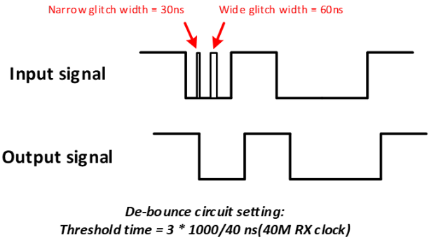
UART Rx Debounce
UART supports Rx debounce to filter glitches in Rx signals. The function can be enabled by asserting DBNC_FEN bit in UART_RXDBCR register. Rx debounce clock source is the same as the Rx clock source, which can be XTAL 40MHz or OSC 2MHz. DBNC_CYC field in UART_RXDBCR register is set to debounce Rx signals with different glitches.
When DBNC_FEN bit in UART_RXDBCR register is asserted, glitches shorter than DBNC_CYC debounce clock cycles will be filtered as shown below. Meanwhile, delay will be introduced to Rx signal for (DBNC_CYC + 2) debounce clock cycles.
UART Rx debounce
UARTx_BT Used as Normal UART
UART interfaces can be configured to connect internally to the Bluetooth (BT) module for communication. Alternatively, they can be configured as standard UARTs to communicate with external devices.
Note
This feature is not supported by all ICs.
The relevant UART controller can only be configured as normal UART when the BT function is not in use.
UART2_BT is used for internal BT UART by default.
For normal UART usage, set the relevant register described below.
Name: REG_LSYS_BT_CTRL0
Size: 32 bits
Base Address:
0x41008000Address offset:
0x280Read/write access: read/write
Bit |
Name |
Access |
Reset |
Description |
|---|---|---|---|---|
19 |
BT_USE_EXT_UART |
R/W |
0x0 |
|
UART3_BT is used for internal BT UART by default.
For normal UART usage, set the relevant register described below.
Name: REG_LSYS_BT_CTRL0
Size: 32 bits
Base Address:
0x4100C000Address offset:
0x280Read/write access: read/write
Bit |
Name |
Access |
Reset |
Description |
|---|---|---|---|---|
19 |
BT_USE_EXT_UART |
R/W |
0x0 |
|
UARTx_BT is not supported.
UART3_BT is used for internal BT UART by default.
For normal UART usage, set the relevant register described below.
Name: REG_LSYS_BT_CTRL0
Size: 32 bits
Base Address:
0x4080A000Address offset:
0x2B8Read/write access: read/write
Bit |
Name |
Access |
Reset |
Description |
|---|---|---|---|---|
19 |
BT_USE_EXT_UART |
R/W |
0x0 |
|
UARTx_BT is not supported.
Registers
Base Address:
UART0_REG : 0x4100C000
UART1_REG : 0x4100D000
UART2_REG : 0x4100E000
Name |
Address offset |
Access |
Description |
|---|---|---|---|
000h |
R/W |
The low 8 bits of divisor coefficient only valid when the DLAB bit of LCR bit[7] = 1. |
|
004h |
R/W |
Generate enable and disable interrupt by the UART, only valid when the DLAB bit of LCR bit[7] = 0. |
|
008h |
R |
Interrupt source indication |
|
00Ch |
R/W |
Set the general communication parameters |
|
010h |
R/W |
It is used to perform handshaking actions with the attached device. |
|
014h |
R |
Indicate the current state of communication and errors |
|
018h |
R |
It contains information about the four incoming modem control lines on the device. |
|
01Ch |
R/W |
It is used to store Tx information. |
|
020h |
R/W |
It is used to indicate the information of Tx baud rate. |
|
024h |
R/W |
The buffers of received data/transmitted data |
|
028h |
R/W |
It is used to provide DMA and IrDA related information. |
|
02Ch |
R/W |
It is used to indicate the shift value of SIR Tx pulse. |
|
030h |
R/W |
It is used to indicate the threshold of SIR Rx pulse. |
|
034h |
R/W |
It is used to monitor the baud rate of Rx pulse. |
|
03Ch |
R |
||
040h |
R/W |
It is used to monitor the Rx baud rate error and Rx baudrate factor setting. |
|
044h |
R/W |
It is used to monitor the baud rate of Rx path. |
|
048h |
R/W |
It is used to monitor the baud rate of Rx path. |
|
04Ch |
R |
It is used to monitor the clock cycle number of Rx path. |
|
050h |
R/W |
It is used to count the number of data read from RXFIFO (byte). |
|
054h |
R/W |
||
058h |
R/W |
||
05Ch |
R/W |
Added in MP version, not exist in test chip version |
|
060h |
R |
REG_UART_DLL
Name: UART divisor length register
Size: 32
Address offset: 000h
Read/write access: R/W
The low 8 bits of divisor coefficient only valid when the DLAB bit of LCR bit[7] = 1.
Bit |
Symbol |
Access |
INI |
Description |
|---|---|---|---|---|
31:8 |
RSVD |
R |
- |
Reserved |
7:0 |
BAUD |
R/W |
0x0 |
The low 8 bits of divisor coefficient (not used) |
REG_UART_IER
Name: UART interrupt enable register
Size: 32
Address offset: 004h
Read/write access: R/W
Generate enable and disable interrupt by the UART, only valid when the DLAB bit of LCR bit[7] = 0.
Bit |
Symbol |
Access |
INI |
Description |
|---|---|---|---|---|
31:7 |
RSVD |
R |
- |
Reserved |
6 |
ERXNDI |
R/W |
0x0 |
Rx noise detected interrupt enable |
5 |
ETOI |
R/W |
0x0 |
Rx timeout interrupt enable |
4 |
EMDI |
R/W |
0x0 |
Rx path monitor done interrupt enable |
3 |
EDSSI |
R/W |
0x0 |
Modem Status Interrupt (EDSSI) (modem status transition) enable |
2 |
ELSI |
R/W |
0x0 |
Receiver Line Status Interrupt (ELSI) (receiver line status) enable |
1 |
ETBEI |
R/W |
0x0 |
Transmitter FIFO Empty interrupt (ETBEI) (Tx FIFO empty) enable |
0 |
ERBI |
R/W |
0x0 |
Received Data Available Interrupt (ERBFI) (Rx trigger) enable |
REG_UART_IIR
Name: UART interrupt identification register
Size: 32
Address offset: 008h
Read/write access: R
Interrupt source indication
Bit |
Symbol |
Access |
INI |
Description |
|---|---|---|---|---|
31:1 |
RSVD |
R |
- |
Reserved |
0 |
INT_PEND |
R |
0x1 |
|
REG_UART_LCR
Name: UART line control register
Size: 32
Address offset: 00Ch
Read/write access: R/W
Set the general communication parameters
Bit |
Symbol |
Access |
INI |
Description |
|---|---|---|---|---|
31:8 |
RSVD |
R |
- |
Reserved |
7 |
DLAB |
R/W |
0x0 |
Divisor Latch Access bit, and control the accessibility of the DLL, DLM and IER registers
Note THR/RBR don’t care the value of this bit. |
6 |
BRCTL |
R/W |
0x0 |
Break Control bit
|
5 |
STKP |
R/W |
0x0 |
Stick Parity bit
|
4 |
EPS |
R/W |
0x0 |
Even Parity selection
|
3 |
PEN |
R/W |
0x0 |
Parity Enable
|
2 |
STB |
R/W |
0x0 |
Stop bits length selection
Note The receiver always checks the first stop bit only. |
1 |
RSVD |
R |
- |
Reserved |
0 |
WLS0 |
R/W |
0x1 |
Word length selection
|
REG_UART_MCR
Name: UART modem control register
Size: 32
Address offset: 010h
Read/write access: R/W
It is used to perform handshaking actions with the attached device.
Bit |
Symbol |
Access |
INI |
Description |
|---|---|---|---|---|
31:6 |
RSVD |
R |
- |
Reserved |
5 |
AFE |
R/W |
0x0 |
Auto flow control enable |
4 |
LOOP_EN |
R/W |
0x0 |
LoopBack mode
|
3 |
OUT2 |
R/W |
0x0 |
Auxiliary output 2 Bit[3] affects the OUT2_ output in a manner identical to that described above set to 0. In loopback mode, connected to Data Carrier Detect (DCD). |
2 |
OUT1 |
R/W |
0x0 |
Auxiliary output 1 Bit3 affects the OUT1_ output in a manner identical to that described above set to 0. In loopback mode, connected to Ring Indicator (RI). |
1 |
RTS |
R/W |
0x0 |
Request to Send (RTS) signal control
This bit controls the RTS_ output. Bit[1] affects the RTS_ output in a manner identical to that described above set to 0. |
0 |
DTR |
R/W |
0x0 |
This bit controls the DTR output. |
REG_UART_LSR
Name: UART line status register
Size: 32
Address offset: 014h
Read/write access: R
Indicate the current state of communication and errors
Bit |
Symbol |
Access |
INI |
Description |
|---|---|---|---|---|
31:13 |
RSVD |
R |
- |
Reserved |
12 |
RXND_INT |
R |
0 |
This bit is only set when Rx debouncer has detected noise.
|
11 |
MODEM_INT |
R |
0 |
This bit is only set when Modem status is pending.
|
10 |
MONITOR_DONE_INT |
R |
0 |
This bit is only set when Rx Path Monitor Done interrupt is enabled (EMDI is set).
|
9 |
TIMEOUT_INT |
R |
0 |
This bit is only set when Rx Timeout interrupt is enabled (ETOI is set).
|
8 |
RXFIFO_INT |
R |
0 |
This bit is only set when Received Data Available Interrupt interrupt is enabled (ERBI is set).
|
7 |
RXFIFO_ERR |
R |
0 |
Uart_rx_error, depending on the FIFO control register (FCR) bit[0]
|
6 |
TX_NOT_FULL |
R |
1 |
TXFIFO not full indicator |
5 |
TX_EMPTY |
R |
1 |
TXFIFO empty indicator |
4 |
BREAK_INT |
R |
Break Interrupt (BI) indicator
|
|
3 |
FRM_ERR |
R |
Framing Error (FE) indicator
|
|
2 |
PAR_ERR |
R |
Parity Error (PE) indicator
|
|
1 |
OVR_ERR |
R |
Overrun Error (OE) indicator
|
|
0 |
DRDY |
R |
|
REG_UART_MSR
Name: UART modem status register
Size: 32
Address offset: 018h
Read/write access: R
It contains information about the four incoming modem control lines on the device.
Bit |
Symbol |
Access |
INI |
Description |
|---|---|---|---|---|
31:8 |
RSVD |
R |
- |
Reserved |
7 |
R_DCD |
R |
Complement of the DCD input or equals to Out2 in loopback mode. |
|
6 |
R_RI |
R |
Complement of the RI input or equals to Out1 in loopback mode. |
|
5 |
R_DSR |
R |
Complement of the DSR input or equals to DTR in loopback mode. |
|
4 |
R_CTS |
R |
Complement of the CTS input or equals to RTS in loopback mode. |
|
3 |
D_DCD |
R |
|
|
2 |
TERI |
R |
|
|
1 |
D_DSR |
R |
|
|
0 |
D_CTS |
R |
|
REG_UART_SCR
Name: UART scratch pad register
Size: 32
Address offset: 01Ch
Read/write access: R/W
It is used to store Tx information.
Bit |
Symbol |
Access |
INI |
Description |
|---|---|---|---|---|
31:27 |
RSVD |
R |
- |
Reserved |
26:16 |
XFACTOR_ADJ |
R/W |
0x0 |
One factor of baud rate calculation for Tx path |
15:13 |
RSVD |
R |
- |
Reserved |
12:8 |
DBG_SEL |
R/W |
0x0 |
Debug port selection |
7 |
SCRATCH_7 |
R/W |
0x0 |
Clear Rx break signal interrupt status |
6:0 |
SCRATCH_6_0 |
R/W |
0x30 |
|
REG_UART_STS
Name: UART STS register
Size: 32
Address offset: 020h
Read/write access: R/W
It is used to indicate the information of Tx baud rate.
Bit |
Symbol |
Access |
INI |
Description |
|---|---|---|---|---|
31:24 |
RSVD |
R |
- |
Reserved |
23:4 |
XFACTOR |
R/W |
0x1047 |
Factor of baud rate calculation for Tx path |
3:0 |
RSVD |
R |
- |
Reserved |
REG_UART_RBR_OR_UART_THR
Name: UART receiver buffer register/UART transmitter holding register
Size: 32
Address offset: 024h
Read/write access: R/W
The buffers of received data/transmitted data
Bit |
Symbol |
Access |
INI |
Description |
|---|---|---|---|---|
31:8 |
RSVD |
R |
- |
Reserved |
7:0 |
DATABIT |
R/W |
0x0 |
UART_RBR’s Rx data bits or UART_THR’s Tx data bit[7:0] Note Bit[0] is the least significant bit. It is the first bit serially received/transmitted. |
REG_UART_MISCR
Name: UART MISC control register
Size: 32
Address offset: 028h
Read/write access: R/W
It is used to provide DMA and IrDA related information.
Bit |
Symbol |
Access |
INI |
Description |
|---|---|---|---|---|
31 |
RSVD |
R |
- |
Reserved |
30 |
CLR_DUMMY_FLAG |
R/W |
0x0 |
Indicate the clearing of dummy data |
29:22 |
DUMMY_DATA |
R/W |
0x0 |
Store dummy data, when UART is DMA flow controller, dummy data is padded for last RXDMA burst request. |
21 |
RXDMA_OWNER |
R/W |
0x0 |
|
20 |
IRDA_RX_INV |
R/W |
0x0 |
Irda_rx_i reverse input enable |
19 |
IRDA_TX_INV |
R/W |
0x0 |
Irda_tx_o reverse output enable |
18:11 |
RXDMA_BURSTSIZE |
R/W |
0x4 |
RXDMA burstsize, maximum value is half of rxfifo depth. |
10:3 |
TXDMA_BURSTSIZE |
R/W |
0x4 |
TXDMA burstsize, maximum value is 16. |
2 |
RXDMA_EN |
R/W |
0x0 |
RXDMA enable, valid when dma_mode in FCR is 1’b1 |
1 |
TXDMA_EN |
R/W |
0x0 |
TXDMA enable, valid when dma_mode in FCR is 1’b1 |
0 |
IRDA_ENABLE |
R/W |
0x0 |
|
REG_UART_SIR_TX_PWC0
Name: UART IRDA SIR TX pulse width control 0 register
Size: 32
Address offset: 02Ch
Read/write access: R/W
It is used to indicate the shift value of SIR Tx pulse.
Bit |
Symbol |
Access |
INI |
Description |
|---|---|---|---|---|
31 |
UPPERBOUND_SHIFTRIGHT |
R/W |
0x0 |
|
30:16 |
UPPERBOUND_SHIFTVAL |
R/W |
0x0 |
The shift value of SIR TX pulse’s right edge |
15 |
LOWBOUND_SHIFTRIGHT |
R/W |
0x0 |
|
14:0 |
LOWBOUND_SHIFTVAL |
R/W |
0x0 |
The shift value of SIR TX pulse’s left edge |
REG_UART_SIR_RX_PFC
Name: UART IRDA SIR Rx pulse filter control register
Size: 32
Address offset: 030h
Read/write access: R/W
It is used to indicate the threshold of SIR Rx pulse.
Bit |
Symbol |
Access |
INI |
Description |
|---|---|---|---|---|
31:16 |
RSVD |
R |
- |
Reserved |
15:1 |
R_SIR_RX_FILTER_THRS |
R/W |
0x0 |
The threshold of SIR Rx filter, Rx pulse is valid only when Rx pulse width is larger than the threshold. |
0 |
R_SIR_RX_FILTER_EN |
R/W |
0x0 |
IrDA SIR Rx filter enable |
REG_UART_BAUD_MON
Name: UART baud monitor register
Size: 32
Address offset: 034h
Read/write access: R/W
It is used to monitor the baud rate of Rx pulse.
Bit |
Symbol |
Access |
INI |
Description |
|---|---|---|---|---|
31 |
TOGGLE_MON_EN |
R/W |
0x0 |
Toggle monitor enable |
30 |
MON_DATA_VLD |
R |
Indicate valid monitoring data |
|
29:24 |
FALLING_THRESH |
R/W |
0x7 |
Indicate the threshold of Rx data rising edge |
23:12 |
MIN_LOW_PERIOD |
R |
Minimum space of consecutive logic ‘0’ of Rx data |
|
11:0 |
MIN_FALL_SPACE |
R |
Minimum space of adjacent falling edge of Rx data |
REG_UART_DBGR
Name: UART debug register
Size: 32
Address offset: 03Ch
Read/write access: R
Bit |
Symbol |
Access |
INI |
Description |
|---|---|---|---|---|
31:0 |
DBG_UART |
R |
The output value of debug port, depending on dbg_sel value in SCR[2:0] |
REG_UART_RX_PATH_CTRL
Name: UART Rx path control register
Size: 32
Address offset: 040h
Read/write access: R/W
It is used to monitor the Rx baud rate error and Rx baudrate factor setting.
Bit |
Symbol |
Access |
INI |
Description |
|---|---|---|---|---|
31:16 |
R_RXTO_THRS |
R/W |
0x40 |
Indicate the timeout threshold of Rx path, unit in one-bit time |
15:14 |
RSVD |
R |
- |
Reserved |
13:3 |
RXBAUD_ADJ_10_0 |
R/W |
0x0 |
One factor of Baud rate calculation for Rx path, similar with xfactor_adj |
2 |
R_RST_NEWRX_N |
R/W |
0x0 |
Reset new Rx path, low active |
1:0 |
RSVD |
R |
- |
Reserved |
REG_UART_MON_BAUD_CTRL
Name: UART monitor baud rate control register
Size: 32
Address offset: 044h
Read/write access: R/W
It is used to monitor the baud rate of Rx path.
Bit |
Symbol |
Access |
INI |
Description |
|---|---|---|---|---|
31:30 |
RSVD |
R |
- |
Reserved |
29 |
R_UPD_OSC_IN_XTAL |
R/W |
0x0 |
Update parameter r_cycnum_perbit_osc (during the update of parameter r_cycnum_perbit_xtal) enable |
28:9 |
R_CYCNUM_PERBIT_OSC |
R/W |
0x0 |
Indicate the average OSC clock cycle number of one bit, for Rx path OSC clock Note SW sets the initial value, and HW updates it depending on the monitor result. |
8:1 |
R_BIT_NUM_THRES |
R/W |
0x0 |
Indicate the bit number threshold of one monitor period, max value is 127 |
0 |
R_MON_BAUD_EN |
R/W |
0x0 |
Monitor Rx baud enable |
REG_UART_MON_BAUD_STS
Name: UART monitor baud rate status register
Size: 32
Address offset: 048h
Read/write access: R/W
It is used to monitor the baud rate of Rx path.
Bit |
Symbol |
Access |
INI |
Description |
|---|---|---|---|---|
31:29 |
RSVD |
R |
- |
Reserved |
28:21 |
RO_MON_TOTAL_BIT |
R |
0x0 |
Indicate the number of bits actually monitored |
20 |
RO_MON_RDY |
R |
0x0 |
Indicate the finish of calculation of actual cycle number per bit, it’s cleared when r_mon_baud_en is 0. |
19:0 |
R_CYCNUM_PERBIT_XTAL |
R/W |
0x0 |
Indicate the fractional xtal clock cycle number of one bit, for Rx path XTAL clock Note SW sets the initial value, and HW updates it depending on the monitor result. |
REG_UART_MON_CYC_NUM
Name: UART monitored cycle number register
Size: 32
Address offset: 04Ch
Read/write access: R
It is used to monitor the clock cycle number of Rx path.
Bit |
Symbol |
Access |
INI |
Description |
|---|---|---|---|---|
31:28 |
RSVD |
R |
- |
Reserved |
27:0 |
RO_MON_TOTAL_CYCLE |
R |
Indicate the number of clock cycle actually monitored |
REG_UART_RX_BYTE_CNT
Name: UART Rx data byte count register
Size: 32
Address offset: 050h
Read/write access: R/W
It is used to count the number of data read from RXFIFO (byte).
Bit |
Symbol |
Access |
INI |
Description |
|---|---|---|---|---|
31:17 |
RSVD |
R |
- |
Reserved |
16 |
CLR_RX_BYTE_CNT |
R/W |
Write 1 to clear ro_rx_byte_cnt |
|
15:0 |
RO_RX_BYTE_CNT |
R |
Count the byte number of data read from RXFIFO |
REG_UART_FCR
Name: UART FIFO control register
Size: 32
Address offset: 054h
Read/write access: R/W
Bit |
Symbol |
Access |
INI |
Description |
|---|---|---|---|---|
31:8 |
RSVD |
R |
- |
Reserved |
7:6 |
RECVTRG |
R/W |
0x3 |
Define the 16-entries Receiver FIFO Interrupt trigger level (0~15 bytes)
|
5:4 |
RSVD |
R |
- |
Reserved |
3 |
DMA_MODE |
R/W |
0x0 |
Support DMA mode (co-operate with DW DDMA in the data path) |
2 |
XMIT_CLR |
R/W |
0x0 |
Clear xmitckt |
1 |
RECV_CLR |
R/W |
0x0 |
Clear receiving |
0 |
FIFO_EN |
R/W |
0x1 |
Error report of RCVR FIFO field enable, only valid when the LSR bit[7] is set to 1. |
REG_UART_ICR
Name: UART interrupt clear register
Size: 32
Address offset: 058h
Read/write access: R/W
Bit |
Symbol |
Access |
INI |
Description |
|---|---|---|---|---|
31:5 |
RSVD |
R |
- |
Reserved |
4 |
RXNDICF |
R/W |
0x0 |
Rx noise Detected Interrupt Flag |
3 |
MDICF |
R/W |
0x0 |
Monitor Done Interrupt Flag |
2 |
MICF |
R/W |
0x0 |
Modem Interrupt Clear Flag |
1 |
TOICF |
R/W |
0x0 |
Timeout Interrupt Clear Flag |
0 |
RLSICF |
R/W |
0x0 |
Receiver Line Statue Interrupt Clear Flag Writing 1 to this bit clears PARITY_ERR, OVERRUN_ERR, FRAMING_ERR, BREAK_ERR_INT and RXFIFO_ERR in the USART_LSR register. |
REG_UART_RXDBCR
Name: UART RX debounce control register
Size: 32
Address offset: 05Ch
Read/write access: R/W
Added in MP version, not exist in test chip version
Bit |
Symbol |
Access |
INI |
Description |
|---|---|---|---|---|
31:16 |
RSVD |
R |
- |
Reserved |
15:1 |
DBNC_CYC |
R/W |
0xF |
Debounce cycles in unit of sclk |
0 |
DBNC_FEN |
R/W |
0x0 |
UART Rx debounce enable |
REG_UART_DUMMY
Name: UART Dummy Register
Size: 32
Address offset: 060h
Read/write access: R
Bit |
Symbol |
Access |
INI |
Description |
|---|---|---|---|---|
31:16 |
RSVD |
R |
- |
Reserved |
15:0 |
DUMMY |
R |
0x0 |
Reserved for HW |
Base Address:
UART0_REG : 0x41010000
UART1_REG : 0x41011000
UART2_REG : 0x41012000
UART3_REG : 0x41013000
Name |
Address offset |
Access |
Description |
|---|---|---|---|
000h |
R/W |
The low 8 bits of divisor coefficient only valid when the DLAB bit of LCR bit[7] = 1 |
|
004h |
R/W |
Generate enable and disable interrupt by the UART, only valid when the DLAB bit of LCR bit[7] = 0. |
|
008h |
R |
Interrupt source indication |
|
00Ch |
R/W |
Set the general communication parameters |
|
010h |
R/W |
It is used to perform handshaking actions with the attached device. |
|
014h |
R |
Indicate the current state of communication and errors |
|
018h |
R |
It contains information about the four incoming modem control lines on the device |
|
01Ch |
R/W |
It is used to store information of TX |
|
020h |
R/W |
Indicate the information of Tx baud rate |
|
024h |
R/W |
The buffers of received data / The buffers of transmitted data |
|
028h |
R/W |
Provide DMA and IrDA related information |
|
02Ch |
R/W |
Indicates the shift value of SIR Tx pulse |
|
030h |
R/W |
Indicates the threshold of SIR Rx pulse |
|
034h |
R/W |
Monitor the baud rate of Rx pulse |
|
03Ch |
R |
||
040h |
R/W |
Monitor the Rx baud rate error and Rx baudrate factor setting |
|
044h |
R/W |
Monitor the baud rate of Rx path |
|
048h |
R/W |
Monitor the baud rate of Rx path |
|
04Ch |
R |
Monitored clock cycle number of Rx path |
|
050h |
R/W |
Count the number of data read from rxfifo (byte) |
|
054h |
R/W |
FIFO control |
|
058h |
R/W |
Interrupt clear |
|
05Ch |
R/W |
REG_UART_DLL
Name: UART divisor length register
Size: 32
Address offset: 000h
Read/write access: R/W
The low 8 bits of divisor coefficient only valid when the DLAB bit of LCR bit[7] = 1
Bit |
Symbol |
Access |
INI |
Description |
|---|---|---|---|---|
31:8 |
RSVD |
R |
- |
Reserved |
7:0 |
BAUD |
R/W |
0x0 |
The low 8 bits of divisor coefficient (not used) |
REG_UART_IER
Name: UART interrupt enable register
Size: 32
Address offset: 004h
Read/write access: R/W
Generate enable and disable interrupt by the UART, only valid when the DLAB bit of LCR bit[7] = 0.
Bit |
Symbol |
Access |
INI |
Description |
|---|---|---|---|---|
31:7 |
RSVD |
R |
- |
Reserved |
6 |
ERXNDI |
R/W |
0x0 |
Rx noise detected interrupt enable |
5 |
ETOI |
R/W |
0x0 |
Rx timeout interrupt enable |
4 |
EMDI |
R/W |
0x0 |
Rx path monitor done interrupt enable |
3 |
EDSSI |
R/W |
0x0 |
Modem Status Interrupt (EDSSI) (modem status transition) enable |
2 |
ELSI |
R/W |
0x0 |
Receiver Line Status Interrupt (ELSI) (receiver line status) enable |
1 |
ETBEI |
R/W |
0x0 |
Transmitter FIFO Empty interrupt (ETBEI) (Tx FIFO empty) enable |
0 |
ERBI |
R/W |
0x0 |
Received Data Available Interrupt (ERBFI) (Rx trigger) enable |
REG_UART_IIR
Name: UART interrupt identification register
Size: 32
Address offset: 008h
Read/write access: R
Interrupt source indication
Bit |
Symbol |
Access |
INI |
Description |
|---|---|---|---|---|
31:1 |
RSVD |
R |
- |
Reserved |
0 |
INT_PEND |
R |
0x1 |
|
REG_UART_LCR
Name: UART line control register
Size: 32
Address offset: 00Ch
Read/write access: R/W
Set the general communication parameters
Bit |
Symbol |
Access |
INI |
Description |
|---|---|---|---|---|
31:16 |
DUMMY |
R/W |
0x00FF |
Dummy |
15:8 |
RSVD |
R |
- |
Reserved |
7 |
DLAB |
R/W |
0x0 |
Divisor Latch Access bit, and control the accessibility of the DLL, DLM and IER registers
Note THR/RBR don’t care the value of this bit. |
6 |
BRCTL |
R/W |
0x0 |
Break Control bit
|
5 |
STKP |
R/W |
0x0 |
Stick Parity bit
|
4 |
EPS |
R/W |
0x0 |
Even Parity selection
|
3 |
PEN |
R/W |
0x0 |
Parity Enable
|
2 |
STB |
R/W |
0x0 |
Stop bits length selection
Note The receiver always checks the first stop bit only. |
1 |
RSVD |
R |
- |
Reserved |
0 |
WLS0 |
R/W |
0x1 |
Word length selection
|
REG_UART_MCR
Name: UART modem control register
Size: 32
Address offset: 010h
Read/write access: R/W
It is used to perform handshaking actions with the attached device.
Bit |
Symbol |
Access |
INI |
Description |
|---|---|---|---|---|
31:6 |
RSVD |
R |
- |
Reserved |
5 |
AFE |
R/W |
0x0 |
Auto flow control enable |
4 |
LOOP_EN |
R/W |
0x0 |
LoopBack mode
|
3 |
OUT2 |
R/W |
0x0 |
Auxiliary output 2 Bit[3] affects the OUT2_ output in a manner identical to that described above set to 0 In loopback mode, connected to Data Carrier Detect (DCD). |
2 |
OUT1 |
R/W |
0x0 |
Auxiliary output 1 Bit[3] affects the OUT1_ output in a manner identical to that described above set to 0 In loopback mode, connected to Ring Indicator (RI) |
1 |
RTS |
R/W |
0x0 |
Request to Send (RTS) signal control
This bit controls the RTS_ output. Bit[1] affects the RTS_ output in a manner identical to that described above set to 0. |
0 |
DTR |
R/W |
0x0 |
This bit controls the DTR output |
REG_UART_LSR
Name: UART line status register
Size: 32
Address offset: 014h
Read/write access: R
Indicate the current state of communication and errors
Bit |
Symbol |
Access |
INI |
Description |
|---|---|---|---|---|
31:13 |
RSVD |
R |
- |
Reserved |
12 |
RXND_INT |
R |
0 |
This bit is only set when RX debouncer has detected noise
|
11 |
MODEM_INT |
R |
0 |
This bit is only set when Modem status pending
|
10 |
MONITOR_DONE_INT |
R |
0 |
This bit is only set when Rx Path Monitor Done interrupt is enabled(EMDI is set)
|
9 |
TIMEOUT_INT |
R |
0 |
This bit is only set when Rx Timeout interrupt is enabled(ETOI is set)
|
8 |
RXFIFO_INT |
R |
0 |
This bit is only set when Received Data Available Interrupt interrupt is enabled(ERBI is set)
|
7 |
RXFIFO_ERR |
R |
0 |
Uart_rx_error, depending on the FIFO control register (FCR) bit[0]
|
6 |
TX_NOT_FULL |
R |
1 |
TXFIFO not full indicator |
5 |
TX_EMPTY |
R |
1 |
TXFIFO empty indicator |
4 |
BREAK_INT |
R |
Break Interrupt (BI) indicator
|
|
3 |
FRM_ERR |
R |
Framing Error (FE) indicator
|
|
2 |
PAR_ERR |
R |
Parity Error (PE) indicator
|
|
1 |
OVR_ERR |
R |
Overrun Error (OE) indicator
|
|
0 |
DRDY |
R |
|
REG_UART_MSR
Name: UART modem status register
Size: 32
Address offset: 018h
Read/write access: R
It contains information about the four incoming modem control lines on the device
Bit |
Symbol |
Access |
INI |
Description |
|---|---|---|---|---|
31:8 |
RSVD |
R |
- |
Reserved |
7 |
R_DCD |
R |
Complement of the DCD input or equals to Out2 in loopback mode. |
|
6 |
R_RI |
R |
Complement of the RI input or equals to Out1 in loopback mode. |
|
5 |
R_DSR |
R |
Complement of the DSR input or equals to DTR in loopback mode. |
|
4 |
R_CTS |
R |
Complement of the CTS input or equals to RTS in loopback mode. |
|
3 |
D_DCD |
R |
|
|
2 |
TERI |
R |
|
|
1 |
D_DSR |
R |
|
|
0 |
D_CTS |
R |
|
REG_UART_SCR
Name: UART scratch pad register
Size: 32
Address offset: 01Ch
Read/write access: R/W
It is used to store information of TX
Bit |
Symbol |
Access |
INI |
Description |
|---|---|---|---|---|
31:27 |
RSVD |
R |
- |
Reserved |
26:16 |
XFACTOR_ADJ |
R/W |
0x0 |
One factor of Baud rate calculation for Tx path |
15:13 |
RSVD |
R |
- |
Reserved |
12:8 |
DBG_SEL |
R/W |
0x0 |
Debug port selection |
7 |
SCRATCH_7 |
R/W |
0x0 |
Clear Rx break signal interrupt status |
6:0 |
SCRATCH_6_0 |
R/W |
0x30 |
|
REG_UART_STS
Name: UART STS register
Size: 32
Address offset: 020h
Read/write access: R/W
Indicate the information of Tx baud rate
Bit |
Symbol |
Access |
INI |
Description |
|---|---|---|---|---|
31:24 |
RSVD |
R |
- |
Reserved |
23:4 |
XFACTOR |
R/W |
0x1047 |
Factor of Baud rate calculation for Tx path |
3:0 |
RSVD |
R |
- |
Reserved |
REG_UART_RBR_OR_UART_THR
Name: UART receiver buffer register/UART transmitter holding register
Size: 32
Address offset: 024h
Read/write access: R/W
The buffers of received data / The buffers of transmitted data
Bit |
Symbol |
Access |
INI |
Description |
|---|---|---|---|---|
31:8 |
RSVD |
R |
- |
Reserved |
7:0 |
DATABIT |
R/W |
0x0 |
UART_RBR’s Rx data bits or UART_THR’s Tx data bit[7:0] Note Bit[0] is the least significant bit. It is the first bit serially received/transmitted. |
REG_UART_MISCR
Name: UART MISC control register
Size: 32
Address offset: 028h
Read/write access: R/W
Provide DMA and IrDA related information
Bit |
Symbol |
Access |
INI |
Description |
|---|---|---|---|---|
31 |
RSVD |
R |
- |
Reserved |
30 |
CLR_DUMMY_FLAG |
R/W |
0x0 |
Indicate the clearing of dummy data |
29:22 |
DUMMY_DATA |
R/W |
0x0 |
Store dummy data, when UART is DMA flow controller, dummy data is padded for last RXDMA burst request. |
21 |
RXDMA_OWNER |
R/W |
0x0 |
|
20 |
IRDA_RX_INV |
R/W |
0x0 |
Irda_rx_i reverse input enable |
19 |
IRDA_TX_INV |
R/W |
0x0 |
Irda_tx_o reverse output enable |
18:11 |
RXDMA_BURSTSIZE |
R/W |
0x4 |
RXDMA burstsize, maximum value is half of rxfifo depth. |
10:3 |
TXDMA_BURSTSIZE |
R/W |
0x4 |
TXDMA burstsize, maximum value is 16. |
2 |
RXDMA_EN |
R/W |
0x0 |
RXDMA enable, valid when dma_mode in FCR is 1’b1 |
1 |
TXDMA_EN |
R/W |
0x0 |
TXDMA enable, valid when dma_mode in FCR is 1’b1 |
0 |
IRDA_ENABLE |
R/W |
0x0 |
|
REG_UART_SIR_TX_PWC0
Name: UART IRDA SIR TX pulse width control 0 register
Size: 32
Address offset: 02Ch
Read/write access: R/W
Indicates the shift value of SIR Tx pulse
Bit |
Symbol |
Access |
INI |
Description |
|---|---|---|---|---|
31 |
UPPERBOUND_SHIFTRIGHT |
R/W |
0x0 |
|
30:16 |
UPPERBOUND_SHIFTVAL |
R/W |
0x0 |
The shift value of SIR Tx pulse’s right edge |
15 |
LOWBOUND_SHIFTRIGHT |
R/W |
0x0 |
|
14:0 |
LOWBOUND_SHIFTVAL |
R/W |
0x0 |
The shift value of SIR Tx pulse’s left edge |
REG_UART_SIR_RX_PFC
Name: UART IRDA SIR Rx pulse filter control register
Size: 32
Address offset: 030h
Read/write access: R/W
Indicates the threshold of SIR Rx pulse
Bit |
Symbol |
Access |
INI |
Description |
|---|---|---|---|---|
31:16 |
RSVD |
R |
- |
Reserved |
15:1 |
R_SIR_RX_FILTER_THRS |
R/W |
0x0 |
The threshold of SIR Rx filter, Rx pulse is valid only when Rx pulse width is larger than the threshold. |
0 |
R_SIR_RX_FILTER_EN |
R/W |
0x0 |
IrDA SIR Rx filter enable |
REG_UART_BAUD_MON
Name: UART baud monitor register
Size: 32
Address offset: 034h
Read/write access: R/W
Monitor the baud rate of Rx pulse
Bit |
Symbol |
Access |
INI |
Description |
|---|---|---|---|---|
31 |
TOGGLE_MON_EN |
R/W |
0x0 |
Toggle monitor enable |
30 |
MON_DATA_VLD |
R |
Indicate valid monitoring data |
|
29:24 |
FALLING_THRESH |
R/W |
0x7 |
Indicate the threshold of Rx data rising edge |
23:12 |
MIN_LOW_PERIOD |
R |
Minimum space of consecutive logic ‘0’ of Rx data |
|
11:0 |
MIN_FALL_SPACE |
R |
Minimum space of adjacent falling edge of Rx data |
REG_UART_DBGR
Name: UART debug register
Size: 32
Address offset: 03Ch
Read/write access: R
Bit |
Symbol |
Access |
INI |
Description |
|---|---|---|---|---|
31:0 |
DBG_UART |
R |
The output value of debug port, depending on dbg_sel value in SCR[2:0] |
REG_UART_RX_PATH_CTRL
Name: UART Rx path control register
Size: 32
Address offset: 040h
Read/write access: R/W
Monitor the Rx baud rate error and Rx baudrate factor setting
Bit |
Symbol |
Access |
INI |
Description |
|---|---|---|---|---|
31:16 |
R_RXTO_THRS |
R/W |
0x40 |
Indicate the timeout threshold of Rx path, unit in one-bit time |
15:14 |
RSVD |
R |
- |
Reserved |
13:3 |
RXBAUD_ADJ_10_0 |
R/W |
0x0 |
One factor of Baud rate calculation for Rx path, similar with xfactor_adj |
2 |
R_RST_NEWRX_N |
R/W |
0x0 |
Reset new Rx path, low active |
1:0 |
RSVD |
R |
- |
Reserved |
REG_UART_MON_BAUD_CTRL
Name: UART monitor baud rate control register
Size: 32
Address offset: 044h
Read/write access: R/W
Monitor the baud rate of Rx path
Bit |
Symbol |
Access |
INI |
Description |
|---|---|---|---|---|
31:30 |
RSVD |
R |
- |
Reserved |
29 |
R_UPD_OSC_IN_XTAL |
R/W |
0x0 |
Update parameter r_cycnum_perbit_osc (during the update of parameter r_cycnum_perbit_xtal) enable |
28:9 |
R_CYCNUM_PERBIT_OSC |
R/W |
0x0 |
Indicate the average OSC clock cycle number of one bit, for Rx path OSC clk Note SW sets the initial value, HW updates it depending on the monitor result. |
8:1 |
R_BIT_NUM_THRES |
R/W |
0x0 |
Indicate the bit number threshold of one monitor period, max value is 127 |
0 |
R_MON_BAUD_EN |
R/W |
0x0 |
Monitor Rx baud enable |
REG_UART_MON_BAUD_STS
Name: UART monitor baud rate status register
Size: 32
Address offset: 048h
Read/write access: R/W
Monitor the baud rate of Rx path
Bit |
Symbol |
Access |
INI |
Description |
|---|---|---|---|---|
31:29 |
RSVD |
R |
- |
Reserved |
28:21 |
RO_MON_TOTAL_BIT |
R |
0x0 |
Indicate the number of bits actually monitored |
20 |
RO_MON_RDY |
R |
0x0 |
Indicate the finish of calculation of actual cycle number per bit, it’s cleared when r_mon_baud_en is 0 |
19:0 |
R_CYCNUM_PERBIT_XTAL |
R/W |
0x0 |
Indicate the fractional xtal clock cycle number of one bit, for Rx path xtal clk Note SW sets the initial value, HW updates it depending on the monitor result. |
REG_UART_MON_CYC_NUM
Name: UART monitored cycle number register
Size: 32
Address offset: 04Ch
Read/write access: R
Monitored clock cycle number of Rx path
Bit |
Symbol |
Access |
INI |
Description |
|---|---|---|---|---|
31:28 |
RSVD |
R |
- |
Reserved |
27:0 |
RO_MON_TOTAL_CYCLE |
R |
Indicate the number of clock cycle actually monitored |
REG_UART_RX_BYTE_CNT
Name: UART Rx data byte count register
Size: 32
Address offset: 050h
Read/write access: R/W
Count the number of data read from rxfifo (byte)
Bit |
Symbol |
Access |
INI |
Description |
|---|---|---|---|---|
31:17 |
RSVD |
R |
- |
Reserved |
16 |
CLR_RX_BYTE_CNT |
R/W |
Write 1 to clear ro_rx_byte_cnt |
|
15:0 |
RO_RX_BYTE_CNT |
R |
Count the byte number of data read from RXFIFO |
REG_UART_FCR
Name: UART FIFO control register
Size: 32
Address offset: 054h
Read/write access: R/W
FIFO control
Bit |
Symbol |
Access |
INI |
Description |
|---|---|---|---|---|
31:8 |
RSVD |
R |
- |
Reserved |
7:6 |
RECVTRG |
R/W |
0x3 |
Define the 16-entries Receiver FIFO Interrupt trigger level (0~15 bytes)
|
5:4 |
RSVD |
R |
- |
Reserved |
3 |
DMA_MODE |
R/W |
0x0 |
Support dma mode (cooperating with DW DDMA in the data path) |
2 |
XMIT_CLR |
R/W |
0x0 |
Clear xmitckt |
1 |
RECV_CLR |
R/W |
0x0 |
Clear receiving |
0 |
FIFO_EN |
R/W |
0x1 |
Error report of RCVR FIFO field enable, only valid when the LSR bit[7] is set to 1. |
REG_UART_ICR
Name: UART interrupt clear register
Size: 32
Address offset: 058h
Read/write access: R/W
Interrupt clear
Bit |
Symbol |
Access |
INI |
Description |
|---|---|---|---|---|
31:5 |
RSVD |
R |
- |
Reserved |
4 |
RXNDICF |
R/W |
0x0 |
Rx noise Detected Interrupt Flag |
3 |
MDICF |
R/W |
0x0 |
Monitor Done Interrupt Flag |
2 |
MICF |
R/W |
0x0 |
Modem Interrupt Clear Flag |
1 |
TOICF |
R/W |
0x0 |
Timeout Interrupt Clear Flag |
0 |
RLSICF |
R/W |
0x0 |
Receiver Line Statue Interrupt Clear Flag Writing 1 to this bit clears PARITY_ERR, OVERRUN_ERR, FRAMING_ERR, BREAK_ERR_INT and RXFIFO_ERR in the USART_LSR register. |
REG_UART_RXDBCR
Name: UART RX debounce control register
Size: 32
Address offset: 05Ch
Read/write access: R/W
Bit |
Symbol |
Access |
INI |
Description |
|---|---|---|---|---|
31:16 |
RSVD |
R |
- |
Reserved |
15:1 |
DBNC_CYC |
R/W |
0xF |
Debounce cycles in unit of sclk |
0 |
DBNC_FEN |
R/W |
0x0 |
UART RX debounce enable |
REGISTER_CONTENTS=RTL8720E
REGISTER_CONTENTS=RTL8720E
REGISTER_CONTENTS=RTL8720E
Base Address:
UART0_REG : 0x41004000
UART1_REG : 0x41005000
UART2_REG : 0x41006000
UART3_REG : 0x41007000
Name |
Address offset |
Access |
Description |
|---|---|---|---|
000h |
R/W |
The low 8 bits of divisor coefficient only valid when the DLAB bit of LCR bit[7] = 1 |
|
004h |
R/W |
Generate enable and disable interrupt by the UART, only valid when the DLAB bit of LCR bit[7] = 0. |
|
008h |
R |
Interrupt source indication |
|
00Ch |
R/W |
Set the general communication parameters |
|
010h |
R/W |
It is used to perform handshaking actions with the attached device. |
|
014h |
R |
Indicate the current state of communication and errors |
|
018h |
R |
It contains information about the four incoming modem control lines on the device |
|
01Ch |
R/W |
It is used to store information of TX |
|
020h |
R/W |
Indicate the information of TX baud rate |
|
024h |
R/W |
The buffers of received data / The buffers of transmitted data |
|
028h |
R/W |
Provide DMA and IrDA related information |
|
02Ch |
R/W |
Indicates the shift value of SIR TX pulse |
|
030h |
R/W |
Indicates the threshold of SIR Rx pulse |
|
034h |
R/W |
Monitor the baud rate of Rx pulse |
|
03Ch |
R |
Debug |
|
040h |
R/W |
Monitor the Rx baud rate error and Rx baudrate factor setting |
|
044h |
R/W |
Monitor the baud rate of Rx path |
|
048h |
R/W |
Monitor the baud rate of Rx path |
|
04Ch |
R |
Monitored clock cycle number of Rx path |
|
050h |
R/W |
Count the number of data read from rxfifo (byte) |
|
054h |
R/W |
FIFO control |
|
058h |
R/W |
Interrupt clear |
|
05Ch |
R/W |
Added in MP version, not existed in Test chip version |
REG_UART_DLL
Name: UART divisor length register
Size: 32
Address offset: 000h
Read/write access: R/W
The low 8 bits of divisor coefficient only valid when the DLAB bit of LCR bit[7] = 1
Bit |
Symbol |
Access |
INI |
Description |
|---|---|---|---|---|
31:8 |
RSVD |
R |
- |
Reserved |
7:0 |
BAUD |
R/W |
0x0 |
The low 8 bits of divisor coefficient (not used) |
REG_UART_IER
Name: UART interrupt enable register
Size: 32
Address offset: 004h
Read/write access: R/W
Generate enable and disable interrupt by the UART, only valid when the DLAB bit of LCR bit[7] = 0.
Bit |
Symbol |
Access |
INI |
Description |
|---|---|---|---|---|
31:7 |
RSVD |
R |
- |
Reserved |
6 |
ERXNDI |
R/W |
0x0 |
Rx noise detected interrupt enable |
5 |
ETOI |
R/W |
0x0 |
Rx timeout interrupt enable |
4 |
EMDI |
R/W |
0x0 |
Rx path monitor done interrupt enable |
3 |
EDSSI |
R/W |
0x0 |
Modem Status Interrupt (EDSSI) (modem status transition) enable |
2 |
ELSI |
R/W |
0x0 |
Receiver Line Status Interrupt (ELSI) (receiver line status) enable |
1 |
ETBEI |
R/W |
0x0 |
Transmitter FIFO Empty interrupt (ETBEI) (tx fifo empty) enable |
0 |
ERBI |
R/W |
0x0 |
Received Data Available Interrupt (ERBFI) (rx trigger) enable |
REG_UART_IIR
Name: UART interrupt identification register
Size: 32
Address offset: 008h
Read/write access: R
Interrupt source indication
Bit |
Symbol |
Access |
INI |
Description |
|---|---|---|---|---|
31:1 |
RSVD |
R |
- |
Reserved |
0 |
INT_PEND |
R |
0x1 |
|
REG_UART_LCR
Name: UART line control register
Size: 32
Address offset: 00Ch
Read/write access: R/W
Set the general communication parameters
Bit |
Symbol |
Access |
INI |
Description |
|---|---|---|---|---|
31:8 |
RSVD |
R |
- |
Reserved |
7 |
DLAB |
R/W |
0x0 |
Divisor Latch Access bit, and control the accessibility of the DLL, DLM and IER registers
Note THR/RBR don’t care the value of dlab bit. |
6 |
BRCTL |
R/W |
0x0 |
Break Control bit
|
5 |
STKP |
R/W |
0x0 |
Stick Parity bit
|
4 |
EPS |
R/W |
0x0 |
Even Parity selection
|
3 |
PEN |
R/W |
0x0 |
Parity Enable
|
2 |
STB |
R/W |
0x0 |
Stop bits length selection
Note The receiver always checks the first stop bit only. |
1 |
RSVD |
R |
- |
Reserved |
0 |
WLS0 |
R/W |
0x1 |
Word length selection
|
REG_UART_MCR
Name: UART modem control register
Size: 32
Address offset: 010h
Read/write access: R/W
It is used to perform handshaking actions with the attached device.
Bit |
Symbol |
Access |
INI |
Description |
|---|---|---|---|---|
31:6 |
RSVD |
R |
- |
Reserved |
5 |
AFE |
R/W |
0x0 |
Auto flow control enable |
4 |
LOOP_EN |
R/W |
0x0 |
LoopBack mode
|
3 |
OUT2 |
R/W |
0x0 |
Auxiliary output 2 Bit[3] affects the OUT2_ output in a manner identical to that described above set to 0 In loopback mode, connected to Data Carrier Detect (DCD). |
2 |
OUT1 |
R/W |
0x0 |
Auxiliary output 1 Bit3 affects the OUT1_ output in a manner identical to that described above set to 0 In loopback mode, connected to Ring Indicator (RI) |
1 |
RTS |
R/W |
0x0 |
Request to Send (RTS) signal control
This bit controls the RTS_ output. Bit[1] affects the RTS_ output in a manner identical to that described above set to 0. |
0 |
DTR |
R/W |
0x0 |
This bit controls the DTR output |
REG_UART_LSR
Name: UART line status register
Size: 32
Address offset: 014h
Read/write access: R
Indicate the current state of communication and errors
Bit |
Symbol |
Access |
INI |
Description |
|---|---|---|---|---|
31:13 |
RSVD |
R |
- |
Reserved |
12 |
RXND_INT |
R |
0 |
This bit is only set when RX debouncer has detected noise
|
11 |
MODEM_INT |
R |
0 |
This bit is only set when Modem status pending
|
10 |
MONITOR_DONE_INT |
R |
0 |
This bit is only set when Rx Path Monitor Done interrupt is enabled(EMDI is set)
|
9 |
TIMEOUT_INT |
R |
0 |
This bit is only set when Rx Timeout interrupt is enabled(ETOI is set)
|
8 |
RXFIFO_INT |
R |
0 |
This bit is only set when Received Data Available Interrupt interrupt is enabled(ERBI is set)
|
7 |
RXFIFO_ERR |
R |
0 |
Uart_rx_error, depending on the FIFO control register (FCR) bit[0]
|
6 |
TX_NOT_FULL |
R |
1 |
TXFIFO not full indicator |
5 |
TX_EMPTY |
R |
1 |
TXFIFO empty indicator |
4 |
BREAK_INT |
R |
Break Interrupt (BI) indicator
|
|
3 |
FRM_ERR |
R |
Framing Error (FE) indicator
|
|
2 |
PAR_ERR |
R |
Parity Error (PE) indicator
|
|
1 |
OVR_ERR |
R |
Overrun Error (OE) indicator
|
|
0 |
DRDY |
R |
|
REG_UART_MSR
Name: UART modem status register
Size: 32
Address offset: 018h
Read/write access: R
It contains information about the four incoming modem control lines on the device
Bit |
Symbol |
Access |
INI |
Description |
|---|---|---|---|---|
31:8 |
RSVD |
R |
- |
Reserved |
7 |
R_DCD |
R |
Complement of the DCD input or equals to Out2 in loopback mode. |
|
6 |
R_RI |
R |
Complement of the RI input or equals to Out1 in loopback mode. |
|
5 |
R_DSR |
R |
Complement of the DSR input or equals to DTR in loopback mode. |
|
4 |
R_CTS |
R |
Complement of the CTS input or equals to RTS in loopback mode. |
|
3 |
D_DCD |
R |
|
|
2 |
TERI |
R |
|
|
1 |
D_DSR |
R |
|
|
0 |
D_CTS |
R |
|
REG_UART_SCR
Name: UART scratch pad register
Size: 32
Address offset: 01Ch
Read/write access: R/W
It is used to store information of TX
Bit |
Symbol |
Access |
INI |
Description |
|---|---|---|---|---|
31:27 |
RSVD |
R |
- |
Reserved |
26:16 |
XFACTOR_ADJ |
R/W |
0x0 |
One factor of Baud rate calculation for TX path |
15:13 |
RSVD |
R |
- |
Reserved |
12:8 |
DBG_SEL |
R/W |
0x0 |
Debug port selection |
7 |
SCRATCH_7 |
R/W |
0x0 |
Clear rx break signal interrupt status |
6:0 |
SCRATCH_6_0 |
R/W |
0x30 |
|
REG_UART_STS
Name: UART STS register
Size: 32
Address offset: 020h
Read/write access: R/W
Indicate the information of TX baud rate
Bit |
Symbol |
Access |
INI |
Description |
|---|---|---|---|---|
31:24 |
RSVD |
R |
- |
Reserved |
23:4 |
XFACTOR |
R/W |
0x1047 |
Factor of Baud rate calculation for Tx path |
3:0 |
RSVD |
R |
- |
Reserved |
REG_UART_RBR_OR_UART_THR
Name: UART receiver buffer register/UART transmitter holding register
Size: 32
Address offset: 024h
Read/write access: R/W
The buffers of received data / The buffers of transmitted data
Bit |
Symbol |
Access |
INI |
Description |
|---|---|---|---|---|
31:8 |
RSVD |
R |
- |
Reserved |
7:0 |
DATABIT |
R/W |
0x0 |
UART_RBR’s Rx data bits or UART_THR’s Tx data bit[7:0] Note Bit[0] is the least significant bit. It is the first bit serially received/transmitted. |
REG_UART_MISCR
Name: UART MISC control register
Size: 32
Address offset: 028h
Read/write access: R/W
Provide DMA and IrDA related information
Bit |
Symbol |
Access |
INI |
Description |
|---|---|---|---|---|
31 |
RSVD |
R |
- |
Reserved |
30 |
CLR_DUMMY_FLAG |
R/W |
0x0 |
Indicate the clearing of dummy data |
29:22 |
DUMMY_DATA |
R/W |
0x0 |
Store dummy data, when UART is DMA flow controller, dummy data is padded for last RXDMA burst request. |
21 |
RXDMA_OWNER |
R/W |
0x0 |
|
20 |
IRDA_RX_INV |
R/W |
0x0 |
Irda_rx_i reverse input enable |
19 |
IRDA_TX_INV |
R/W |
0x0 |
Irda_tx_o reverse output enable |
18:11 |
RXDMA_BURSTSIZE |
R/W |
0x4 |
RXDMA burstsize, maximum value is half of rxfifo depth. |
10:3 |
TXDMA_BURSTSIZE |
R/W |
0x4 |
TXDMA burstsize, maximum value is 16. |
2 |
RXDMA_EN |
R/W |
0x0 |
RXDMA enable, valid when dma_mode in FCR is 1’b1 |
1 |
TXDMA_EN |
R/W |
0x0 |
TXDMA enable, valid when dma_mode in FCR is 1’b1 |
0 |
IRDA_ENABLE |
R/W |
0x0 |
|
REG_UART_SIR_TX_PWC0
Name: UART IRDA SIR TX pulse width control 0 register
Size: 32
Address offset: 02Ch
Read/write access: R/W
Indicates the shift value of SIR TX pulse
Bit |
Symbol |
Access |
INI |
Description |
|---|---|---|---|---|
31 |
UPPERBOUND_SHIFTRIGHT |
R/W |
0x0 |
|
30:16 |
UPPERBOUND_SHIFTVAL |
R/W |
0x0 |
The shift value of SIR TX pulse’s right edge |
15 |
LOWBOUND_SHIFTRIGHT |
R/W |
0x0 |
|
14:0 |
LOWBOUND_SHIFTVAL |
R/W |
0x0 |
The shift value of SIR TX pulse’s left edge |
REG_UART_SIR_RX_PFC
Name: UART IRDA SIR Rx pulse filter control register
Size: 32
Address offset: 030h
Read/write access: R/W
Indicates the threshold of SIR Rx pulse
Bit |
Symbol |
Access |
INI |
Description |
|---|---|---|---|---|
31:16 |
RSVD |
R |
- |
Reserved |
15:1 |
R_SIR_RX_FILTER_THRS |
R/W |
0x0 |
The threshold of SIR Rx filter, Rx pulse is valid only when Rx pulse width is larger than the threshold. |
0 |
R_SIR_RX_FILTER_EN |
R/W |
0x0 |
IrDA SIR Rx filter enable |
REG_UART_BAUD_MON
Name: UART baud monitor register
Size: 32
Address offset: 034h
Read/write access: R/W
Monitor the baud rate of Rx pulse
Bit |
Symbol |
Access |
INI |
Description |
|---|---|---|---|---|
31 |
TOGGLE_MON_EN |
R/W |
0x0 |
Toggle monitor enable |
30 |
MON_DATA_VLD |
R |
Indicate valid monitoring data |
|
29:24 |
FALLING_THRESH |
R/W |
0x7 |
Indicate the threshold of Rx data rising edge |
23:12 |
MIN_LOW_PERIOD |
R |
Minimum space of consecutive logic ‘0’ of Rx data |
|
11:0 |
MIN_FALL_SPACE |
R |
Minimum space of adjacent falling edge of Rx data |
REG_UART_DBGR
Name: UART debug register
Size: 32
Address offset: 03Ch
Read/write access: R
Debug
Bit |
Symbol |
Access |
INI |
Description |
|---|---|---|---|---|
31:0 |
DBG_UART |
R |
The output value of debug port, depending on dbg_sel value in SCR[2:0] |
REG_UART_RX_PATH_CTRL
Name: UART Rx path control register
Size: 32
Address offset: 040h
Read/write access: R/W
Monitor the Rx baud rate error and Rx baudrate factor setting
Bit |
Symbol |
Access |
INI |
Description |
|---|---|---|---|---|
31:16 |
R_RXTO_THRS |
R/W |
0x40 |
Indicate the timeout threshold of Rx path, unit in one-bit time |
15:14 |
RSVD |
R |
- |
Reserved |
13:3 |
RXBAUD_ADJ_10_0 |
R/W |
0x0 |
One factor of Baud rate calculation for Rx path, similar with xfactor_adj |
2 |
R_RST_NEWRX_N |
R/W |
0x0 |
Reset new Rx path, low active |
1:0 |
RSVD |
R |
- |
Reserved |
REG_UART_MON_BAUD_CTRL
Name: UART monitor baud rate control register
Size: 32
Address offset: 044h
Read/write access: R/W
Monitor the baud rate of Rx path
Bit |
Symbol |
Access |
INI |
Description |
|---|---|---|---|---|
31:30 |
RSVD |
R |
- |
Reserved |
29 |
R_UPD_OSC_IN_XTAL |
R/W |
0x0 |
Update parameter r_cycnum_perbit_osc (during the update of parameter r_cycnum_perbit_xtal) enable |
28:9 |
R_CYCNUM_PERBIT_OSC |
R/W |
0x0 |
Indicate the average OSC clock cycle number of one bit, for Rx path OSC clk Note SW sets the initial value, HW updates it depending on the monitor result. |
8:1 |
R_BIT_NUM_THRES |
R/W |
0x0 |
Indicate the bit number threshold of one monitor period, max value is 127 |
0 |
R_MON_BAUD_EN |
R/W |
0x0 |
Monitor Rx baud enable |
REG_UART_MON_BAUD_STS
Name: UART monitor baud rate status register
Size: 32
Address offset: 048h
Read/write access: R/W
Monitor the baud rate of Rx path
Bit |
Symbol |
Access |
INI |
Description |
|---|---|---|---|---|
31:29 |
RSVD |
R |
- |
Reserved |
28:21 |
RO_MON_TOTAL_BIT |
R |
0x0 |
Indicate the number of bits actually monitored |
20 |
RO_MON_RDY |
R |
0x0 |
Indicate the finish of calculation of actual cycle number per bit, it’s cleared when r_mon_baud_en is 0 |
19:0 |
R_CYCNUM_PERBIT_XTAL |
R/W |
0x0 |
Indicate the fractional xtal clock cycle number of one bit, for Rx path xtal clk Note SW sets the initial value, HW updates it depending on the monitor result. |
REG_UART_MON_CYC_NUM
Name: UART monitored cycle number register
Size: 32
Address offset: 04Ch
Read/write access: R
Monitored clock cycle number of Rx path
Bit |
Symbol |
Access |
INI |
Description |
|---|---|---|---|---|
31:28 |
RSVD |
R |
- |
Reserved |
27:0 |
RO_MON_TOTAL_CYCLE |
R |
Indicate the number of clock cycle actually monitored |
REG_UART_RX_BYTE_CNT
Name: UART Rx data byte count register
Size: 32
Address offset: 050h
Read/write access: R/W
Count the number of data read from rxfifo (byte)
Bit |
Symbol |
Access |
INI |
Description |
|---|---|---|---|---|
31:17 |
RSVD |
R |
- |
Reserved |
16 |
CLR_RX_BYTE_CNT |
R/W |
Write 1 to clear ro_rx_byte_cnt |
|
15:0 |
RO_RX_BYTE_CNT |
R |
Count the byte number of data read from rxfifo |
REG_UART_FCR
Name: UART FIFO control register
Size: 32
Address offset: 054h
Read/write access: R/W
FIFO control
Bit |
Symbol |
Access |
INI |
Description |
|---|---|---|---|---|
31:8 |
RSVD |
R |
- |
Reserved |
7:6 |
RECVTRG |
R/W |
0x3 |
Define the 16-entries Receiver FIFO Interrupt trigger level (0~15 bytes)
|
5:4 |
RSVD |
R |
- |
Reserved |
3 |
DMA_MODE |
R/W |
0x0 |
Support dma mode (cooperate with DW DDMA in the data path) |
2 |
XMIT_CLR |
R/W |
0x0 |
Clear xmitckt |
1 |
RECV_CLR |
R/W |
0x0 |
Clear receiving |
0 |
FIFO_EN |
R/W |
0x1 |
Error report of RCVR FIFO field enable, only valid when the LSR bit[7] is set to 1. |
REG_UART_ICR
Name: UART interrupt clear register
Size: 32
Address offset: 058h
Read/write access: R/W
Interrupt clear
Bit |
Symbol |
Access |
INI |
Description |
|---|---|---|---|---|
31:5 |
RSVD |
R |
- |
Reserved |
4 |
RXNDICF |
R/W |
0x0 |
Rx noise Detected Interrupt Flag |
3 |
MDICF |
R/W |
0x0 |
Monitor Done Interrupt Flag |
2 |
MICF |
R/W |
0x0 |
Modem Interrupt Clear Flag |
1 |
TOICF |
R/W |
0x0 |
Timeout Interrupt Clear Flag |
0 |
RLSICF |
R/W |
0x0 |
Receiver Line Statue Interrupt Clear Flag Writing 1 to this bit clears PARITY_ERR, OVERRUN_ERR, FRAMING_ERR, BREAK_ERR_INT and RXFIFO_ERR in the USART_LSR register. |
REG_UART_RXDBCR
Name: UART RX debounce control register
Size: 32
Address offset: 05Ch
Read/write access: R/W
Added in MP version, not existed in Test chip version
Bit |
Symbol |
Access |
INI |
Description |
|---|---|---|---|---|
31:16 |
RSVD |
R |
- |
Reserved |
15:1 |
DBNC_CYC |
R/W |
0xF |
Debounce cycles in unit of sclk |
0 |
DBNC_FEN |
R/W |
0x0 |
UART RX debounce enable |
Base Address:
UART0_REG : 0x4080C000
UART1_REG : 0x4080D000
UART2_REG : 0x4080E000
UART3_REG : 0x4080F000
Name |
Address offset |
Access |
Description |
|---|---|---|---|
000h |
R/W |
The low 8 bits of divisor coefficient only valid when the DLAB bit of LCR bit[7] = 1 |
|
004h |
R/W |
Generate enable and disable interrupt by the UART, only valid when the DLAB bit of LCR bit[7] = 0. |
|
008h |
R |
Interrupt source indication |
|
00Ch |
R/W |
Set the general communication parameters |
|
010h |
R/W |
It is used to perform handshaking actions with the attached device. |
|
014h |
R |
Indicate the current state of communication and errors |
|
018h |
R |
It contains information about the four incoming modem control lines on the device |
|
01Ch |
R/W |
It is used to store information of TX |
|
020h |
R/W |
Indicate the information of TX baud rate |
|
024h |
R/W |
The buffers of received data / The buffers of transmitted data |
|
028h |
R/W |
Provide DMA and IrDA related information |
|
02Ch |
R/W |
Indicates the shift value of SIR TX pulse |
|
030h |
R/W |
Indicates the threshold of SIR Rx pulse |
|
034h |
R/W |
Monitor the baud rate of Rx pulse |
|
03Ch |
R |
Debug |
|
040h |
R/W |
Monitor the Rx baud rate error and Rx baudrate factor setting |
|
044h |
R/W |
Monitor the baud rate of Rx path |
|
048h |
R/W |
Monitor the baud rate of Rx path |
|
04Ch |
R |
Monitored clock cycle number of Rx path |
|
050h |
R/W |
Count the number of data read from rxfifo (byte) |
|
054h |
R/W |
FIFO control |
|
058h |
R/W |
Interrupt clear |
|
05Ch |
R/W |
Added in MP version, not existed in Test chip version |
|
060h |
R/W |
||
064h |
R |
REG_UART_DLL
Name: UART divisor length register
Size: 32
Address offset: 000h
Read/write access: R/W
The low 8 bits of divisor coefficient only valid when the DLAB bit of LCR bit[7] = 1
Bit |
Symbol |
Access |
INI |
Description |
|---|---|---|---|---|
31:8 |
RSVD |
R |
- |
Reserved |
7:0 |
BAUD |
R/W |
0x0 |
The low 8 bits of divisor coefficient (not used) |
REG_UART_IER
Name: UART interrupt enable register
Size: 32
Address offset: 004h
Read/write access: R/W
Generate enable and disable interrupt by the UART, only valid when the DLAB bit of LCR bit[7] = 0.
Bit |
Symbol |
Access |
INI |
Description |
|---|---|---|---|---|
31:8 |
RSVD |
R |
- |
Reserved |
7 |
ERETI |
R/W |
0x0 |
RXFIFO_EMPTY_TIMEOUT interrupt enable |
6 |
ERXNDI |
R/W |
0x0 |
Rx noise detected interrupt enable |
5 |
ETOI |
R/W |
0x0 |
Rx timeout interrupt enable |
4 |
EMDI |
R/W |
0x0 |
Rx path monitor done interrupt enable |
3 |
EDSSI |
R/W |
0x0 |
Modem Status Interrupt (EDSSI) (modem status transition) enable |
2 |
ELSI |
R/W |
0x0 |
Receiver Line Status Interrupt (ELSI) (receiver line status) enable |
1 |
ETBEI |
R/W |
0x0 |
Transmitter FIFO Empty interrupt (ETBEI) (Tx FIFO empty) enable |
0 |
ERBI |
R/W |
0x0 |
Received Data Available Interrupt (ERBFI) (Rx trigger) enable |
REG_UART_IIR
Name: UART interrupt identification register
Size: 32
Address offset: 008h
Read/write access: R
Interrupt source indication
Bit |
Symbol |
Access |
INI |
Description |
|---|---|---|---|---|
31:1 |
RSVD |
R |
- |
Reserved |
0 |
INT_PEND |
R |
0x1 |
|
REG_UART_LCR
Name: UART line control register
Size: 32
Address offset: 00Ch
Read/write access: R/W
Set the general communication parameters
Bit |
Symbol |
Access |
INI |
Description |
|---|---|---|---|---|
31:8 |
RSVD |
R |
- |
Reserved |
7 |
DLAB |
R/W |
0x0 |
Divisor Latch Access bit, and control the accessibility of the DLL, DLM and IER registers
Note THR/RBR don’t care the value of dlab bit. |
6 |
BRCTL |
R/W |
0x0 |
Break Control bit
|
5 |
STKP |
R/W |
0x0 |
Stick Parity bit
|
4 |
EPS |
R/W |
0x0 |
Even Parity selection
|
3 |
PEN |
R/W |
0x0 |
Parity Enable
|
2 |
STB |
R/W |
0x0 |
Stop bits length selection
Note The receiver always checks the first stop bit only. |
1 |
RSVD |
R |
- |
Reserved |
0 |
WLS0 |
R/W |
0x1 |
Word length selection
|
REG_UART_MCR
Name: UART modem control register
Size: 32
Address offset: 010h
Read/write access: R/W
It is used to perform handshaking actions with the attached device.
Bit |
Symbol |
Access |
INI |
Description |
|---|---|---|---|---|
31:6 |
RSVD |
R |
- |
Reserved |
5 |
AFE |
R/W |
0x0 |
Auto flow control enable |
4 |
LOOP_EN |
R/W |
0x0 |
LoopBack mode
|
3 |
OUT2 |
R/W |
0x0 |
Auxiliary output 2 Bit[3] affects the OUT2_ output in a manner identical to that described above set to 0 In loopback mode, connected to Data Carrier Detect (DCD). |
2 |
OUT1 |
R/W |
0x0 |
Auxiliary output 1 Bit3 affects the OUT1_ output in a manner identical to that described above set to 0 In loopback mode, connected to Ring Indicator (RI) |
1 |
RTS |
R/W |
0x0 |
Request to Send (RTS) signal control
This bit controls the RTS_ output. Bit[1] affects the RTS_ output in a manner identical to that described above set to 0. |
0 |
DTR |
R/W |
0x0 |
This bit controls the DTR output |
REG_UART_LSR
Name: UART line status register
Size: 32
Address offset: 014h
Read/write access: R
Indicate the current state of communication and errors
Bit |
Symbol |
Access |
INI |
Description |
|---|---|---|---|---|
31:14 |
RSVD |
R |
- |
Reserved |
13 |
RE_TIMEOUT_INT |
R |
0 |
This bit is only set when rxfifo empty timeout interrupt is enabled(ERETI is set)
|
12 |
RXND_INT |
R |
0 |
This bit is only set when RX debouncer has detected noise
|
11 |
MODEM_INT |
R |
0 |
This bit is only set when Modem status pending
|
10 |
MONITOR_DONE_INT |
R |
0 |
This bit is only set when Rx Path Monitor Done interrupt is enabled(EMDI is set)
|
9 |
TIMEOUT_INT |
R |
0 |
This bit is only set when Rx Timeout interrupt is enabled(ETOI is set)
|
8 |
RXFIFO_INT |
R |
0 |
This bit is only set when Received Data Available Interrupt interrupt is enabled(ERBI is set)
|
7 |
RXFIFO_ERR |
R |
0 |
Uart_rx_error, depending on the FIFO control register (FCR) bit[0]
|
6 |
TX_NOT_FULL |
R |
1 |
TXFIFO not full indicator |
5 |
TX_EMPTY |
R |
1 |
TXFIFO empty indicator |
4 |
BREAK_INT |
R |
Break Interrupt (BI) indicator
|
|
3 |
FRM_ERR |
R |
Framing Error (FE) indicator
|
|
2 |
PAR_ERR |
R |
Parity Error (PE) indicator
|
|
1 |
OVR_ERR |
R |
Overrun Error (OE) indicator
|
|
0 |
DRDY |
R |
|
REG_UART_MSR
Name: UART modem status register
Size: 32
Address offset: 018h
Read/write access: R
It contains information about the four incoming modem control lines on the device
Bit |
Symbol |
Access |
INI |
Description |
|---|---|---|---|---|
31:8 |
RSVD |
R |
- |
Reserved |
7 |
R_DCD |
R |
Complement of the DCD input or equals to Out2 in loopback mode. |
|
6 |
R_RI |
R |
Complement of the RI input or equals to Out1 in loopback mode. |
|
5 |
R_DSR |
R |
Complement of the DSR input or equals to DTR in loopback mode. |
|
4 |
R_CTS |
R |
Complement of the CTS input or equals to RTS in loopback mode. |
|
3 |
D_DCD |
R |
|
|
2 |
TERI |
R |
|
|
1 |
D_DSR |
R |
|
|
0 |
D_CTS |
R |
|
REG_UART_SCR
Name: UART scratch pad register
Size: 32
Address offset: 01Ch
Read/write access: R/W
It is used to store information of TX
Bit |
Symbol |
Access |
INI |
Description |
|---|---|---|---|---|
31:27 |
RSVD |
R |
- |
Reserved |
26:16 |
XFACTOR_ADJ |
R/W |
0x0 |
One factor of Baud rate calculation for TX path |
15:13 |
RSVD |
R |
- |
Reserved |
12:8 |
DBG_SEL |
R/W |
0x0 |
Debug port selection |
7 |
SCRATCH_7 |
R/W |
0x0 |
Clear rx break signal interrupt status |
6:0 |
SCRATCH_6_0 |
R/W |
0x30 |
|
REG_UART_STS
Name: UART STS register
Size: 32
Address offset: 020h
Read/write access: R/W
Indicate the information of TX baud rate
Bit |
Symbol |
Access |
INI |
Description |
|---|---|---|---|---|
31:24 |
RSVD |
R |
- |
Reserved |
23:4 |
XFACTOR |
R/W |
0x1047 |
Factor of Baud rate calculation for Tx path |
3:0 |
RSVD |
R |
- |
Reserved |
REG_UART_RBR_OR_UART_THR
Name: UART receiver buffer register/UART transmitter holding register
Size: 32
Address offset: 024h
Read/write access: R/W
The buffers of received data / The buffers of transmitted data
Bit |
Symbol |
Access |
INI |
Description |
|---|---|---|---|---|
31:8 |
RSVD |
R |
- |
Reserved |
7:0 |
DATABIT |
R/W |
0x0 |
UART_RBR’s Rx data bits or UART_THR’s Tx data bit[7:0] Note Bit[0] is the least significant bit. It is the first bit serially received/transmitted. |
REG_UART_MISCR
Name: UART MISC control register
Size: 32
Address offset: 028h
Read/write access: R/W
Provide DMA and IrDA related information
Bit |
Symbol |
Access |
INI |
Description |
|---|---|---|---|---|
31 |
RSVD |
R |
- |
Reserved |
30 |
CLR_DUMMY_FLAG |
R/W |
0x0 |
Indicate the clearing of dummy data |
29:22 |
DUMMY_DATA |
R/W |
0x0 |
Store dummy data, when UART is DMA flow controller, dummy data is padded for last RXDMA burst request. |
21 |
RXDMA_OWNER |
R/W |
0x0 |
|
20 |
IRDA_RX_INV |
R/W |
0x0 |
Irda_rx_i reverse input enable |
19 |
IRDA_TX_INV |
R/W |
0x0 |
Irda_tx_o reverse output enable |
18:11 |
RXDMA_BURSTSIZE |
R/W |
0x4 |
RXDMA burstsize, maximum value is half of rxfifo depth. |
10:3 |
TXDMA_BURSTSIZE |
R/W |
0x4 |
TXDMA burstsize, maximum value is 16. |
2 |
RXDMA_EN |
R/W |
0x0 |
RXDMA enable, valid when dma_mode in FCR is 1’b1 |
1 |
TXDMA_EN |
R/W |
0x0 |
TXDMA enable, valid when dma_mode in FCR is 1’b1 |
0 |
IRDA_ENABLE |
R/W |
0x0 |
|
REG_UART_SIR_TX_PWC0
Name: UART IRDA SIR TX pulse width control 0 register
Size: 32
Address offset: 02Ch
Read/write access: R/W
Indicates the shift value of SIR TX pulse
Bit |
Symbol |
Access |
INI |
Description |
|---|---|---|---|---|
31 |
UPPERBOUND_SHIFTRIGHT |
R/W |
0x0 |
|
30:16 |
UPPERBOUND_SHIFTVAL |
R/W |
0x0 |
The shift value of SIR TX pulse’s right edge |
15 |
LOWBOUND_SHIFTRIGHT |
R/W |
0x0 |
|
14:0 |
LOWBOUND_SHIFTVAL |
R/W |
0x0 |
The shift value of SIR TX pulse’s left edge |
REG_UART_SIR_RX_PFC
Name: UART IRDA SIR Rx pulse filter control register
Size: 32
Address offset: 030h
Read/write access: R/W
Indicates the threshold of SIR Rx pulse
Bit |
Symbol |
Access |
INI |
Description |
|---|---|---|---|---|
31:16 |
RSVD |
R |
- |
Reserved |
15:1 |
R_SIR_RX_FILTER_THRS |
R/W |
0x0 |
The threshold of SIR Rx filter, Rx pulse is valid only when Rx pulse width is larger than the threshold. |
0 |
R_SIR_RX_FILTER_EN |
R/W |
0x0 |
IrDA SIR Rx filter enable |
REG_UART_BAUD_MON
Name: UART baud monitor register
Size: 32
Address offset: 034h
Read/write access: R/W
Monitor the baud rate of Rx pulse
Bit |
Symbol |
Access |
INI |
Description |
|---|---|---|---|---|
31 |
TOGGLE_MON_EN |
R/W |
0x0 |
Toggle monitor enable |
30 |
MON_DATA_VLD |
R |
Indicate valid monitoring data |
|
29:24 |
FALLING_THRESH |
R/W |
0x7 |
Indicate the threshold of Rx data rising edge |
23:12 |
MIN_LOW_PERIOD |
R |
Minimum space of consecutive logic ‘0’ of Rx data |
|
11:0 |
MIN_FALL_SPACE |
R |
Minimum space of adjacent falling edge of Rx data |
REG_UART_DBGR
Name: UART debug register
Size: 32
Address offset: 03Ch
Read/write access: R
Debug
Bit |
Symbol |
Access |
INI |
Description |
|---|---|---|---|---|
31:0 |
DBG_UART |
R |
The output value of debug port, depending on dbg_sel value in SCR[2:0] |
REG_UART_RX_PATH_CTRL
Name: UART Rx path control register
Size: 32
Address offset: 040h
Read/write access: R/W
Monitor the Rx baud rate error and Rx baudrate factor setting
Bit |
Symbol |
Access |
INI |
Description |
|---|---|---|---|---|
31:16 |
R_RXTO_THRS |
R/W |
0x40 |
Indicate the timeout threshold of Rx path, unit in one-bit time |
15:14 |
RSVD |
R |
- |
Reserved |
13:3 |
RXBAUD_ADJ_10_0 |
R/W |
0x0 |
One factor of Baud rate calculation for Rx path, similar with xfactor_adj |
2 |
R_RST_NEWRX_N |
R/W |
0x0 |
Reset new Rx path, low active |
1:0 |
RSVD |
R |
- |
Reserved |
REG_UART_MON_BAUD_CTRL
Name: UART monitor baud rate control register
Size: 32
Address offset: 044h
Read/write access: R/W
Monitor the baud rate of Rx path
Bit |
Symbol |
Access |
INI |
Description |
|---|---|---|---|---|
31:30 |
RSVD |
R |
- |
Reserved |
29 |
R_UPD_OSC_IN_XTAL |
R/W |
0x0 |
Update parameter r_cycnum_perbit_osc (during the update of parameter r_cycnum_perbit_xtal) enable |
28:9 |
R_CYCNUM_PERBIT_OSC |
R/W |
0x0 |
Indicate the average OSC clock cycle number of one bit, for Rx path OSC clk Note SW sets the initial value, HW updates it depending on the monitor result. |
8:1 |
R_BIT_NUM_THRES |
R/W |
0x0 |
Indicate the bit number threshold of one monitor period, max value is 127 |
0 |
R_MON_BAUD_EN |
R/W |
0x0 |
Monitor Rx baud enable |
REG_UART_MON_BAUD_STS
Name: UART monitor baud rate status register
Size: 32
Address offset: 048h
Read/write access: R/W
Monitor the baud rate of Rx path
Bit |
Symbol |
Access |
INI |
Description |
|---|---|---|---|---|
31:29 |
RSVD |
R |
- |
Reserved |
28:21 |
RO_MON_TOTAL_BIT |
R |
0x0 |
Indicate the number of bits actually monitored |
20 |
RO_MON_RDY |
R |
0x0 |
Indicate the finish of calculation of actual cycle number per bit, it’s cleared when r_mon_baud_en is 0 |
19:0 |
R_CYCNUM_PERBIT_XTAL |
R/W |
0x0 |
Indicate the fractional xtal clock cycle number of one bit, for Rx path xtal clk Note SW sets the initial value, HW updates it depending on the monitor result. |
REG_UART_MON_CYC_NUM
Name: UART monitored cycle number register
Size: 32
Address offset: 04Ch
Read/write access: R
Monitored clock cycle number of Rx path
Bit |
Symbol |
Access |
INI |
Description |
|---|---|---|---|---|
31:28 |
RSVD |
R |
- |
Reserved |
27:0 |
RO_MON_TOTAL_CYCLE |
R |
Indicate the number of clock cycle actually monitored |
REG_UART_RX_BYTE_CNT
Name: UART Rx data byte count register
Size: 32
Address offset: 050h
Read/write access: R/W
Count the number of data read from rxfifo (byte)
Bit |
Symbol |
Access |
INI |
Description |
|---|---|---|---|---|
31:17 |
RSVD |
R |
- |
Reserved |
16 |
CLR_RX_BYTE_CNT |
R/W |
Write 1 to clear ro_rx_byte_cnt |
|
15:0 |
RO_RX_BYTE_CNT |
R |
Count the byte number of data read from rxfifo |
REG_UART_FCR
Name: UART FIFO control register
Size: 32
Address offset: 054h
Read/write access: R/W
FIFO control
Bit |
Symbol |
Access |
INI |
Description |
|---|---|---|---|---|
31:8 |
RSVD |
R |
- |
Reserved |
7:6 |
RECVTRG |
R/W |
0x3 |
Define the 16-entries Receiver FIFO Interrupt trigger level (0~15 bytes)
|
5:4 |
RSVD |
R |
- |
Reserved |
3 |
DMA_MODE |
R/W |
0x0 |
Support dma mode (cooperate with DW DDMA in the data path) |
2 |
XMIT_CLR |
R/W |
0x0 |
Clear xmitckt |
1 |
RECV_CLR |
R/W |
0x0 |
Clear receiving |
0 |
FIFO_EN |
R/W |
0x1 |
Error report of RCVR FIFO field enable, only valid when the LSR bit[7] is set to 1. |
REG_UART_ICR
Name: UART interrupt clear register
Size: 32
Address offset: 058h
Read/write access: R/W
Interrupt clear
Bit |
Symbol |
Access |
INI |
Description |
|---|---|---|---|---|
31:6 |
RSVD |
R |
- |
Reserved |
5 |
RETICF |
R/W |
0x0 |
Rxfifo empty timeout Interrupt Clear Flag |
4 |
RXNDICF |
R/W |
0x0 |
Rx noise Detected Interrupt Flag |
3 |
MDICF |
R/W |
0x0 |
Monitor Done Interrupt Flag |
2 |
MICF |
R/W |
0x0 |
Modem Interrupt Clear Flag |
1 |
TOICF |
R/W |
0x0 |
Timeout Interrupt Clear Flag |
0 |
RLSICF |
R/W |
0x0 |
Receiver Line Statue Interrupt Clear Flag Writing 1 to this bit clears PARITY_ERR, OVERRUN_ERR, FRAMING_ERR, BREAK_ERR_INT and RXFIFO_ERR in the USART_LSR register. |
REG_UART_RXDBCR
Name: UART RX debounce control register
Size: 32
Address offset: 05Ch
Read/write access: R/W
Added in MP version, not existed in Test chip version
Bit |
Symbol |
Access |
INI |
Description |
|---|---|---|---|---|
31:16 |
RSVD |
R |
- |
Reserved |
15:1 |
DBNC_CYC |
R/W |
0xF |
Debounce cycles in unit of sclk |
0 |
DBNC_FEN |
R/W |
0x0 |
UART RX debounce enable |
REG_UART_TH_RETI
Name: UART rxfifo empty interrupt timeout threshold
Size: 32
Address offset: 060h
Read/write access: R/W
Bit |
Symbol |
Access |
INI |
Description |
|---|---|---|---|---|
31:28 |
RSVD |
R |
- |
Reserved |
27:0 |
TH_RETI |
R/W |
0x0 |
Set rxfifo empty timeout interrupt, when rxfifo is empty for longer than TH_RETI. Timeout counter works in uart_rclk. |
REG_UART_DUMMY
Name: UART Dummy Register
Size: 32
Address offset: 064h
Read/write access: R
Bit |
Symbol |
Access |
INI |
Description |
|---|---|---|---|---|
31:16 |
RSVD |
R |
- |
Reserved |
15:0 |
DUMMY |
R |
0x0 |
Rsvd for hw |
Base Address:
UART0_REG : 0x401C3000
UART1_REG : 0x401C4000
UART2_REG : 0x401C5000
Name |
Address offset |
Access |
Description |
|---|---|---|---|
000h |
R/W |
The low 8 bits of divisor coefficient only valid when the DLAB bit of LCR bit[7] = 1 |
|
004h |
R/W |
Generate enable and disable interrupt by the UART, only valid when the DLAB bit of LCR bit[7] = 0. |
|
008h |
R |
Interrupt source indication |
|
00Ch |
R/W |
Set the general communication parameters |
|
010h |
R/W |
It is used to perform handshaking actions with the attached device. |
|
014h |
R |
Indicate the current state of communication and errors |
|
018h |
R |
It contains information about the four incoming modem control lines on the device |
|
01Ch |
R/W |
It is used to store information of TX |
|
020h |
R/W |
Indicate the information of TX baud rate |
|
024h |
R/W |
The buffers of received data / The buffers of transmitted data |
|
028h |
R/W |
Provide DMA and IrDA related information |
|
02Ch |
R/W |
Indicates the shift value of SIR TX pulse |
|
030h |
R/W |
Indicates the threshold of SIR Rx pulse |
|
034h |
R/W |
Monitor the baud rate of Rx pulse |
|
03Ch |
R |
Debug |
|
040h |
R/W |
Monitor the Rx baud rate error and Rx baudrate factor setting |
|
044h |
R/W |
Monitor the baud rate of Rx path |
|
048h |
R/W |
Monitor the baud rate of Rx path |
|
04Ch |
R |
Monitored clock cycle number of Rx path |
|
050h |
R/W |
Count the number of data read from rxfifo (byte) |
|
054h |
R/W |
FIFO control |
|
058h |
R/W |
Interrupt clear |
|
05Ch |
R/W |
Added in MP version, not existed in Test chip version |
|
060h |
R/W |
||
064h |
R/W |
||
068h |
R |
||
06Ch |
R/W |
||
0F0h |
R |
REG_UART_DLL
Name: UART divisor length register
Size: 32
Address offset: 000h
Read/write access: R/W
The low 8 bits of divisor coefficient only valid when the DLAB bit of LCR bit[7] = 1
Bit |
Symbol |
Access |
INI |
Description |
|---|---|---|---|---|
31:8 |
RSVD |
R |
- |
Reserved |
7:0 |
BAUD |
R/W |
0x0 |
The low 8 bits of divisor coefficient (not used) |
REG_UART_IER
Name: UART interrupt enable register
Size: 32
Address offset: 004h
Read/write access: R/W
Generate enable and disable interrupt by the UART, only valid when the DLAB bit of LCR bit[7] = 0.
Bit |
Symbol |
Access |
INI |
Description |
|---|---|---|---|---|
31:8 |
RSVD |
R |
- |
Reserved |
7 |
ERETI |
R/W |
0x0 |
RXFIFO_EMPTY_TIMEOUT interrupt enable |
6 |
ERXNDI |
R/W |
0x0 |
Rx noise detected interrupt enable |
5 |
ETOI |
R/W |
0x0 |
Rx timeout interrupt enable |
4 |
EMDI |
R/W |
0x0 |
Rx path monitor done interrupt enable |
3 |
EDSSI |
R/W |
0x0 |
Modem Status Interrupt (EDSSI) (modem status transition) enable |
2 |
ELSI |
R/W |
0x0 |
Receiver Line Status Interrupt (ELSI) (receiver line status) enable |
1 |
ETBEI |
R/W |
0x0 |
Transmitter FIFO Empty interrupt (ETBEI) (Tx FIFO empty) enable |
0 |
ERBI |
R/W |
0x0 |
Received Data Available Interrupt (ERBFI) (Rx trigger) enable |
REG_UART_IIR
Name: UART interrupt identification register
Size: 32
Address offset: 008h
Read/write access: R
Interrupt source indication
Bit |
Symbol |
Access |
INI |
Description |
|---|---|---|---|---|
31:1 |
RSVD |
R |
- |
Reserved |
0 |
INT_PEND |
R |
0x1 |
|
REG_UART_LCR
Name: UART line control register
Size: 32
Address offset: 00Ch
Read/write access: R/W
Set the general communication parameters
Bit |
Symbol |
Access |
INI |
Description |
|---|---|---|---|---|
31:8 |
RSVD |
R |
- |
Reserved |
7 |
DLAB |
R/W |
0x0 |
Divisor Latch Access bit, and control the accessibility of the DLL, DLM and IER registers
Note THR/RBR don’t care the value of dlab bit. |
6 |
BRCTL |
R/W |
0x0 |
Break Control bit
|
5 |
STKP |
R/W |
0x0 |
Stick Parity bit
|
4 |
EPS |
R/W |
0x0 |
Even Parity selection
|
3 |
PEN |
R/W |
0x0 |
Parity Enable
|
2 |
STB |
R/W |
0x0 |
Stop bits length selection
Note The receiver always checks the first stop bit only. |
1 |
RSVD |
R |
- |
Reserved |
0 |
WLS0 |
R/W |
0x1 |
Word length selection
|
REG_UART_MCR
Name: UART modem control register
Size: 32
Address offset: 010h
Read/write access: R/W
It is used to perform handshaking actions with the attached device.
Bit |
Symbol |
Access |
INI |
Description |
|---|---|---|---|---|
31:6 |
RSVD |
R |
- |
Reserved |
5 |
AFE |
R/W |
0x0 |
Auto flow control enable |
4 |
LOOP_EN |
R/W |
0x0 |
LoopBack mode
|
3 |
OUT2 |
R/W |
0x0 |
Auxiliary output 2 Bit[3] affects the OUT2_ output in a manner identical to that described above set to 0 In loopback mode, connected to Data Carrier Detect (DCD). |
2 |
OUT1 |
R/W |
0x0 |
Auxiliary output 1 Bit3 affects the OUT1_ output in a manner identical to that described above set to 0 In loopback mode, connected to Ring Indicator (RI) |
1 |
RTS |
R/W |
0x0 |
Request to Send (RTS) signal control
This bit controls the RTS_ output. Bit[1] affects the RTS_ output in a manner identical to that described above set to 0. |
0 |
DTR |
R/W |
0x0 |
This bit controls the DTR output |
REG_UART_LSR
Name: UART line status register
Size: 32
Address offset: 014h
Read/write access: R
Indicate the current state of communication and errors
Bit |
Symbol |
Access |
INI |
Description |
|---|---|---|---|---|
31:14 |
RSVD |
R |
- |
Reserved |
13 |
RE_TIMEOUT_INT |
R |
0 |
This bit is only set when rxfifo empty timeout interrupt is enabled(ERETI is set)
|
12 |
RXND_INT |
R |
0 |
This bit is only set when RX debouncer has detected noise
|
11 |
MODEM_INT |
R |
0 |
This bit is only set when Modem status pending
|
10 |
MONITOR_DONE_INT |
R |
0 |
This bit is only set when Rx Path Monitor Done interrupt is enabled(EMDI is set)
|
9 |
TIMEOUT_INT |
R |
0 |
This bit is only set when Rx Timeout interrupt is enabled(ETOI is set)
|
8 |
RXFIFO_INT |
R |
0 |
This bit is only set when Received Data Available Interrupt interrupt is enabled(ERBI is set)
|
7 |
RXFIFO_ERR |
R |
0 |
Uart_rx_error, depending on the FIFO control register (FCR) bit[0]
|
6 |
TX_NOT_FULL |
R |
1 |
TXFIFO not full indicator |
5 |
TX_EMPTY |
R |
1 |
TXFIFO empty indicator |
4 |
BREAK_INT |
R |
Break Interrupt (BI) indicator
|
|
3 |
FRM_ERR |
R |
Framing Error (FE) indicator
|
|
2 |
PAR_ERR |
R |
Parity Error (PE) indicator
|
|
1 |
OVR_ERR |
R |
Overrun Error (OE) indicator
|
|
0 |
DRDY |
R |
|
REG_UART_MSR
Name: UART modem status register
Size: 32
Address offset: 018h
Read/write access: R
It contains information about the four incoming modem control lines on the device
Bit |
Symbol |
Access |
INI |
Description |
|---|---|---|---|---|
31:8 |
RSVD |
R |
- |
Reserved |
7 |
R_DCD |
R |
Complement of the DCD input or equals to Out2 in loopback mode. |
|
6 |
R_RI |
R |
Complement of the RI input or equals to Out1 in loopback mode. |
|
5 |
R_DSR |
R |
Complement of the DSR input or equals to DTR in loopback mode. |
|
4 |
R_CTS |
R |
Complement of the CTS input or equals to RTS in loopback mode. |
|
3 |
D_DCD |
R |
|
|
2 |
TERI |
R |
|
|
1 |
D_DSR |
R |
|
|
0 |
D_CTS |
R |
|
REG_UART_SCR
Name: UART scratch pad register
Size: 32
Address offset: 01Ch
Read/write access: R/W
It is used to store information of TX
Bit |
Symbol |
Access |
INI |
Description |
|---|---|---|---|---|
31:27 |
RSVD |
R |
- |
Reserved |
26:16 |
XFACTOR_ADJ |
R/W |
0x0 |
One factor of Baud rate calculation for TX path |
15:13 |
RSVD |
R |
- |
Reserved |
12:8 |
DBG_SEL |
R/W |
0x0 |
Debug port selection |
7 |
SCRATCH_7 |
R/W |
0x0 |
Clear rx break signal interrupt status |
6:0 |
SCRATCH_6_0 |
R/W |
0x30 |
|
REG_UART_STS
Name: UART STS register
Size: 32
Address offset: 020h
Read/write access: R/W
Indicate the information of TX baud rate
Bit |
Symbol |
Access |
INI |
Description |
|---|---|---|---|---|
31:24 |
RSVD |
R |
- |
Reserved |
23:4 |
XFACTOR |
R/W |
0x1047 |
Factor of Baud rate calculation for Tx path |
3:0 |
RSVD |
R |
- |
Reserved |
REG_UART_RBR_OR_UART_THR
Name: UART receiver buffer register/UART transmitter holding register
Size: 32
Address offset: 024h
Read/write access: R/W
The buffers of received data / The buffers of transmitted data
Bit |
Symbol |
Access |
INI |
Description |
|---|---|---|---|---|
31:8 |
RSVD |
R |
- |
Reserved |
7:0 |
DATABIT |
R/W |
0x0 |
UART_RBR’s Rx data bits or UART_THR’s Tx data bit[7:0] Note Bit[0] is the least significant bit. It is the first bit serially received/transmitted. |
REG_UART_MISCR
Name: UART MISC control register
Size: 32
Address offset: 028h
Read/write access: R/W
Provide DMA and IrDA related information
Bit |
Symbol |
Access |
INI |
Description |
|---|---|---|---|---|
31:30 |
RSVD |
R |
- |
Reserved |
29:22 |
DUMMY_DATA |
R/W |
0x0 |
Store dummy data, when UART is DMA flow controller, dummy data is padded for last RXDMA burst request. |
21 |
RXDMA_OWNER |
R/W |
0x0 |
|
20 |
IRDA_RX_INV |
R/W |
0x0 |
Irda_rx_i reverse input enable |
19 |
IRDA_TX_INV |
R/W |
0x0 |
Irda_tx_o reverse output enable |
18:11 |
RXDMA_BURSTSIZE |
R/W |
0x4 |
RXDMA burstsize, maximum value is half of rxfifo depth. |
10:3 |
TXDMA_BURSTSIZE |
R/W |
0x4 |
TXDMA burstsize, maximum value is 16. |
2 |
RXDMA_EN |
R/W |
0x0 |
RXDMA enable, valid when dma_mode in FCR is 1’b1 |
1 |
TXDMA_EN |
R/W |
0x0 |
TXDMA enable, valid when dma_mode in FCR is 1’b1 |
0 |
IRDA_ENABLE |
R/W |
0x0 |
|
REG_UART_SIR_TX_PWC0
Name: UART IRDA SIR TX pulse width control 0 register
Size: 32
Address offset: 02Ch
Read/write access: R/W
Indicates the shift value of SIR TX pulse
Bit |
Symbol |
Access |
INI |
Description |
|---|---|---|---|---|
31 |
UPPERBOUND_SHIFTRIGHT |
R/W |
0x0 |
|
30:16 |
UPPERBOUND_SHIFTVAL |
R/W |
0x0 |
The shift value of SIR TX pulse’s right edge |
15 |
LOWBOUND_SHIFTRIGHT |
R/W |
0x0 |
|
14:0 |
LOWBOUND_SHIFTVAL |
R/W |
0x0 |
The shift value of SIR TX pulse’s left edge |
REG_UART_SIR_RX_PFC
Name: UART IRDA SIR Rx pulse filter control register
Size: 32
Address offset: 030h
Read/write access: R/W
Indicates the threshold of SIR Rx pulse
Bit |
Symbol |
Access |
INI |
Description |
|---|---|---|---|---|
31:16 |
RSVD |
R |
- |
Reserved |
15:1 |
R_SIR_RX_FILTER_THRS |
R/W |
0x0 |
The threshold of SIR Rx filter, Rx pulse is valid only when Rx pulse width is larger than the threshold. |
0 |
R_SIR_RX_FILTER_EN |
R/W |
0x0 |
IrDA SIR Rx filter enable |
REG_UART_BAUD_MON
Name: UART baud monitor register
Size: 32
Address offset: 034h
Read/write access: R/W
Monitor the baud rate of Rx pulse
Bit |
Symbol |
Access |
INI |
Description |
|---|---|---|---|---|
31 |
TOGGLE_MON_EN |
R/W |
0x0 |
Toggle monitor enable |
30 |
MON_DATA_VLD |
R |
Indicate valid monitoring data |
|
29:24 |
FALLING_THRESH |
R/W |
0x7 |
Indicate the threshold of Rx data rising edge |
23:12 |
MIN_LOW_PERIOD |
R |
Minimum space of consecutive logic ‘0’ of Rx data |
|
11:0 |
MIN_FALL_SPACE |
R |
Minimum space of adjacent falling edge of Rx data |
REG_UART_DBGR
Name: UART debug register
Size: 32
Address offset: 03Ch
Read/write access: R
Debug
Bit |
Symbol |
Access |
INI |
Description |
|---|---|---|---|---|
31:0 |
DBG_UART |
R |
The output value of debug port, depending on dbg_sel value in SCR[2:0] |
REG_UART_RX_PATH_CTRL
Name: UART Rx path control register
Size: 32
Address offset: 040h
Read/write access: R/W
Monitor the Rx baud rate error and Rx baudrate factor setting
Bit |
Symbol |
Access |
INI |
Description |
|---|---|---|---|---|
31:14 |
RSVD |
R |
- |
Reserved |
13:3 |
RXBAUD_ADJ_10_0 |
R/W |
0x0 |
One factor of Baud rate calculation for Rx path, similar with xfactor_adj |
2 |
R_RST_NEWRX_N |
R/W |
0x0 |
Reset new Rx path, low active |
1:0 |
RSVD |
R |
- |
Reserved |
REG_UART_MON_BAUD_CTRL
Name: UART monitor baud rate control register
Size: 32
Address offset: 044h
Read/write access: R/W
Monitor the baud rate of Rx path
Bit |
Symbol |
Access |
INI |
Description |
|---|---|---|---|---|
31:30 |
RSVD |
R |
- |
Reserved |
29 |
R_UPD_OSC_IN_XTAL |
R/W |
0x0 |
Update parameter r_cycnum_perbit_osc (during the update of parameter r_cycnum_perbit_xtal) enable |
28:9 |
R_CYCNUM_PERBIT_OSC |
R/W |
0x0 |
Indicate the average OSC clock cycle number of one bit, for Rx path OSC clk Note SW sets the initial value, HW updates it depending on the monitor result. |
8:1 |
R_BIT_NUM_THRES |
R/W |
0x0 |
Indicate the bit number threshold of one monitor period, max value is 127 |
0 |
R_MON_BAUD_EN |
R/W |
0x0 |
Monitor Rx baud enable |
REG_UART_MON_BAUD_STS
Name: UART monitor baud rate status register
Size: 32
Address offset: 048h
Read/write access: R/W
Monitor the baud rate of Rx path
Bit |
Symbol |
Access |
INI |
Description |
|---|---|---|---|---|
31:29 |
RSVD |
R |
- |
Reserved |
28:21 |
RO_MON_TOTAL_BIT |
R |
0x0 |
Indicate the number of bits actually monitored |
20 |
RO_MON_RDY |
R |
0x0 |
Indicate the finish of calculation of actual cycle number per bit, it’s cleared when r_mon_baud_en is 0 |
19:0 |
R_CYCNUM_PERBIT_XTAL |
R/W |
0x0 |
Indicate the fractional xtal clock cycle number of one bit, for Rx path xtal clk Note SW sets the initial value, HW updates it depending on the monitor result. |
REG_UART_MON_CYC_NUM
Name: UART monitored cycle number register
Size: 32
Address offset: 04Ch
Read/write access: R
Monitored clock cycle number of Rx path
Bit |
Symbol |
Access |
INI |
Description |
|---|---|---|---|---|
31:28 |
RSVD |
R |
- |
Reserved |
27:0 |
RO_MON_TOTAL_CYCLE |
R |
Indicate the number of clock cycle actually monitored |
REG_UART_RX_BYTE_CNT
Name: UART Rx data byte count register
Size: 32
Address offset: 050h
Read/write access: R/W
Count the number of data read from rxfifo (byte)
Bit |
Symbol |
Access |
INI |
Description |
|---|---|---|---|---|
31:17 |
RSVD |
R |
- |
Reserved |
16 |
CLR_RX_BYTE_CNT |
R/W |
Write 1 to clear ro_rx_byte_cnt |
|
15:0 |
RO_RX_BYTE_CNT |
R |
Count the byte number of data read from rxfifo |
REG_UART_FCR
Name: UART FIFO control register
Size: 32
Address offset: 054h
Read/write access: R/W
FIFO control
Bit |
Symbol |
Access |
INI |
Description |
|---|---|---|---|---|
31:8 |
RSVD |
R |
- |
Reserved |
7:6 |
RECVTRG |
R/W |
0x3 |
Define the Receiver FIFO Interrupt trigger level
|
5:4 |
RSVD |
R |
- |
Reserved |
3 |
DMA_MODE |
R/W |
0x0 |
Support dma mode (cooperate with DW DDMA in the data path) |
2 |
XMIT_CLR |
R/W |
0x0 |
Clear xmitckt |
1 |
RECV_CLR |
R/W |
0x0 |
Clear receiving |
0 |
FIFO_EN |
R/W |
0x1 |
Error report of RCVR FIFO field enable, only valid when the LSR bit[7] is set to 1. |
REG_UART_ICR
Name: UART interrupt clear register
Size: 32
Address offset: 058h
Read/write access: R/W
Interrupt clear
Bit |
Symbol |
Access |
INI |
Description |
|---|---|---|---|---|
31:6 |
RSVD |
R |
- |
Reserved |
5 |
RETICF |
R/W |
0x0 |
Rxfifo empty timeout Interrupt Clear Flag |
4 |
RXNDICF |
R/W |
0x0 |
Rx noise Detected Interrupt Flag |
3 |
MDICF |
R/W |
0x0 |
Monitor Done Interrupt Flag |
2 |
MICF |
R/W |
0x0 |
Modem Interrupt Clear Flag |
1 |
TOICF |
R/W |
0x0 |
Timeout Interrupt Clear Flag |
0 |
RLSICF |
R/W |
0x0 |
Receiver Line Statue Interrupt Clear Flag Writing 1 to this bit clears PARITY_ERR, OVERRUN_ERR, FRAMING_ERR, BREAK_ERR_INT and RXFIFO_ERR in the USART_LSR register. |
REG_UART_RXDBCR
Name: UART RX debounce control register
Size: 32
Address offset: 05Ch
Read/write access: R/W
Added in MP version, not existed in Test chip version
Bit |
Symbol |
Access |
INI |
Description |
|---|---|---|---|---|
31:16 |
RSVD |
R |
- |
Reserved |
15:1 |
DBNC_CYC |
R/W |
0xF |
Debounce cycles in unit of sclk |
0 |
DBNC_FEN |
R/W |
0x0 |
UART RX debounce enable |
REG_UART_RXTO_THRS
Name: UART rx timeout threshold
Size: 32
Address offset: 060h
Read/write access: R/W
Bit |
Symbol |
Access |
INI |
Description |
|---|---|---|---|---|
31:28 |
RSVD |
R |
- |
Reserved |
27:0 |
R_RXTO_THRS |
R/W |
0x40 |
Indicate the timeout threshold of Rx path, unit in one-bit time. Set rxfifo empty timeout interrupt, when ERETI=1 and rxfifo is empty for longer than R_RXTO_THRS, unit in one-bit time |
REG_UART_RXDMA_MAX_LEN
Name: UART rxdma max length register
Size: 32
Address offset: 064h
Read/write access: R/W
Bit |
Symbol |
Access |
INI |
Description |
|---|---|---|---|---|
31:22 |
RSVD |
R |
- |
Reserved |
21:0 |
RXDMA_MAX_LEN |
R/W |
0x0 |
If uart is rxdma flow controller, rxdma_last will be asserted when rxdma transmitted bytes equal RXDMA_MAX_LEN |
REG_UART_RXDMA_REMAIN_LEN
Name: UART rxdma remain length register
Size: 32
Address offset: 068h
Read/write access: R
Bit |
Symbol |
Access |
INI |
Description |
|---|---|---|---|---|
31:22 |
RSVD |
R |
- |
Reserved |
21:0 |
RXDMA_REMAIN_LEN |
R |
0x0 |
Rxdma transmitted remain bytes , RXDMA_REMAIN_LEN will be set value of RXDMA_MAX_LEN when DMA transmission is completed(rxdma_last=1) or rxdma_en is disabled. |
REG_UART_CLR_FLAG
Name: UART clear flag register
Size: 32
Address offset: 06Ch
Read/write access: R/W
Bit |
Symbol |
Access |
INI |
Description |
|---|---|---|---|---|
31:1 |
RSVD |
R |
- |
Reserved |
0 |
CLR_DUMMY_FLAG |
R/W |
0x0 |
Indicate the clearing of dummy data |
REG_UART_DUMMY
Name: UART Dummy Register
Size: 32
Address offset: 0F0h
Read/write access: R
Bit |
Symbol |
Access |
INI |
Description |
|---|---|---|---|---|
31:16 |
RSVD |
R |
- |
Reserved |
15:0 |
DUMMY |
R |
0x0 |
Rsvd for hw |
