Intelligent LED Controller
Supported ICs[ RTL8721Dx ][ RTL8720E ][ RTL8710E ][ RTL8726E ][ RTL8713E ][ RTL8730E ]
Introduction
LEDC (Light Emitting Diode Controller) is a dedicated driver module for intelligent externally-controlled LEDs, designed to provide stable and efficient control for applications such as RGB full-color LED strips and pixel screens. The module is compatible with mainstream intelligent externally-controlled LEDs on the market, such as the WS2812 series. It supports independent 256-level brightness adjustment for R/G/B channels of each LED, enabling 256³ = 16777216 true color displays to meet high-precision color rendering requirements. It also supports single-wire cascade driving with a maximum load of 1024 externally-controlled LEDs, accommodating large-scale applications for long LED strips and large screen displays.
Features
Configurable transfer data pulse time and non-data period
Configurable IDLE state output level
Configurable RGB888 display mode and LED refresh time
Up to 8095 data sequence configurations
32 * 24-bit transmit data FIFO
DMA interface with LEDC as DMA flow controller
Operation mode
DMA mode
Interrupt mode
Block Diagram
The block diagram of LEDC is shown in the figure below.

trans_ctrl: configures LED timing, data order, data transfer mode, data length, and LED number
FIFO: 32 * 24-bit FIFO for transmitting LED data
Int_ctrl: indicates FIFO status of the LED controller, including wait data timeout or data overflow exception
data_out: converts input data to logical character ‘0’ and character ‘1’ according to trans_ctrl configuration
Functional Description
Output Timing
The sequence of logic “1” code, logic “0” code, and refresh period varies among intelligent LEDs. The basic sequence decode chart is shown in the figure.
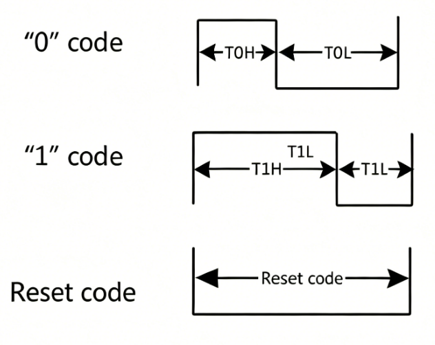
LED decode data sequence chart
In order to generate configurable LED sequence signals, LEDC counts several XTAL40MHz clock periods according to LEDC_T1H_CNT / LEDC_T1L_CNT (register 0x004[31:16]) and LEDC_T0H_CNT / LEDC_T0L_CNT (register 0x004[15:0]) of LEDC_LED_T01_TIMING_CTRL_REG. LEDC output signals are shown in the figure.
LEDC output data format when IDLE state is High
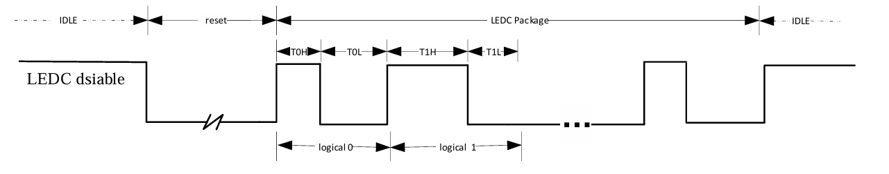
Transfer Timing
The figure below illustrates the LEDC frame output. Before sending a frame of data, a RESET is sent first to refresh the LED. ‘wait_time1’ is used to reduce the refresh rate, and can be disabled by setting LEDC_BIT_WAIT_TIME1_EN (register 0x014[31]) of LEDC_WAIT_TIME1_CTRL_REG to 0. Only the last frame of a scan may contain fewer LEDs than the total LED count.

LEDC output timing diagram of a scan
RESET: A period of time that remains LOW to refresh the LED.
Pixel: 24-bit logical ‘0’ or ‘1’ data decoded into waveforms that form a package or a pixel. LEDs bypass the low level and reshape the high level through the internal signal reshaping amplification circuit.
wait_time0: A period of LOW-level time between two pixel data. This is optional.
wait_time1: A period of LOW-level time after RESET, except for the first frame. This is optional.
Frame: The total number of LEDs. A frame starts after LEDC sends a RESET to the LED.
Scan: Includes all data packages. A scan can contain multiple frames or less than one frame. A scan starts when software configures LEDC and sets
LEDC_BIT_EN(register 0x00[0]) of LEDC_CTRL_REG to 1. The scan stops when LEDC is disabled.
LED Cascade Method
The data mode of LEDC output is based on intelligent LEDs. The typical application circuit of LEDs is shown in the figure.

LED typical application circuit
The supported RGB LEDs use auto-reshaping transmission technology. LEDC sends data in the sequence shown in the figure below, where N represents the number of LEDs driven by LEDC, and Dn represents the data received by the Nth LED.

LEDC data transfer sequence
The intelligent LED captures the first 24-bit data package from Din, reshapes the subsequent data, and outputs it from Dout. To refresh the buffered data of an LED, a RESET must be sent to the LED before new data packages are input at DI.
RGB LED Data Structure
For LEDs, the control circuit and RGB chip are integrated into a single package, forming a complete addressable pixel. Each of the three primary colors per pixel can achieve 256-level brightness display, enabling 16777216-color full-color display.
Each data input is in RGB888 format. LEDC is compatible with different data modes at both input and output ports. By default, 24-bit data is sent in GRB mode, as shown in the figure. The higher bit is transmitted first.

LEDC data MSB order of GRB
Once the LEDC input and output data modes are determined, software sets LEDC_MASK_LED_RGB_MODE (register 0x00[8:6]) of LEDC_CTRL_REG according to the table below.
RGB out mode |
Input GRB |
Input GBR |
Input RGB |
Input RBG |
Input BGR |
Input BRG |
|---|---|---|---|---|---|---|
000 |
GRB |
GBR |
RGB |
RBG |
BGR |
BRG |
001 |
GBR |
GRB |
RBG |
RGB |
BRG |
BGR |
010 |
RGB |
BGR |
GRB |
BRG |
GBR |
RBG |
011 |
BGR |
RGB |
BRG |
GRB |
RBG |
GBR |
100 |
RBG |
BRG |
GBR |
BGR |
GRB |
RGB |
101 |
BRG |
RBG |
BGR |
GBR |
RGB |
GRB |
Operation Mode
LEDC data transfer mode supports DMA mode and CPU interrupt mode, selected by setting LEDC_BIT_DMA_EN (register 0x1C[5]) of LEDC_DMA_CTRL_REG. The internal FIFO depth is 32, and the data width is 24-bit. The FIFO trigger threshold is configured through LEDC_FIFO_TRIG_LEVEL (register 0x1C[4:0]) of LEDC_DMA_CTRL_REG, with a recommended value of 7 or 15.
DMA Mode
When LEDC_BIT_DMA_EN (register 0x1C[5]) of LEDC_DMA_CTRL_REG is set to 1, LEDC enters DMA mode. In this mode, LEDC acts as the flow controller for DMA transfers. The recommended burst length is 8 or 16, and the maximum burst length is 32. When the remaining data to be transferred is greater than or equal to the burst length, and the available space of the internal FIFO is larger than the threshold set by LEDC_FIFO_TRIG_LEVEL, LEDC requests a DMA burst transfer. For each APB write, only the lower 24 bits are valid. When the remaining data to be transferred is less than the burst length and the internal FIFO is not full, LEDC requests a DMA single transfer.
CPU Mode
When LEDC_BIT_DMA_EN (register 0x1C[5]) of LEDC_DMA_CTRL_REG is set to 0, LEDC enters CPU interrupt mode. When the remaining data to be transferred is greater than 0 and the internal FIFO free space is less than the threshold set by LEDC_FIFO_TRIG_LEVEL, LEDC generates a FIFO_CPUREQ_INT in LEDC_LED_INT_STS_REG. Upon receiving this interrupt, the CPU can transfer data from memory to the LEDC FIFO through the APB bus.
LEDC Interrupts
LEDC has four interrupts: FIFO_OVERFLOW_INT, WAITDATA_TIMEOUT_INT, FIFO_CPUREQ_INT, and LEDC_TRANS_FINISH_INT. Each interrupt can be independently masked through the corresponding interrupt enable bit in LEDC_LED_INTERRUPT_CTRL_REG, and globally enabled or disabled through LEDC_BIT_GLOBAL_INT_EN (register 0x020[4]) of LEDC_LED_INTERRUPT_CTRL_REG. When FIFO_OVERFLOW_INT, WAITDATA_TIMEOUT_INT, or LEDC_TRANS_FINISH_INT is generated, the LEDC state machine enters the TRAP state, and software should set LEDC_BIT_SOFT_RESET (register 0x00[1]) of LEDC_CTRL_REG to perform a reset.
Interrupt Descriptions
The trigger conditions and clearing methods for each interrupt are described below:
FIFO overflow interrupt (
FIFO_OVERFLOW_INT) – Asserted when data written externally exceeds the maximum storage space of the LEDC FIFO. LEDC enters a data loss state and transitions to the TRAP state. This interrupt status is cleared by settingLEDC_BIT_SOFT_RESET(register 0x00[1]) of LEDC_CTRL_REG. In DMA mode, this will not occur because the FIFO threshold is set to 1/4 or 1/2 of the desired FIFO depth. LEDC, as a flow controller, sends dma_req based on the FIFO threshold, which matches the DMA source data width and destination data width. In CPU mode, care should be taken that the data to be sent is no more than the remaining FIFO space.Wait data timeout interrupt (
WAITDATA_TIMEOUT_INT) – Asserted when a data request has been sent but data was not pushed to the LEDC FIFO in time. The wait data phase includes wait_time0/1 and wait_data0/1, as shown in the figure below. If the internal FIFO of LEDC cannot receive data due to some abnormal situation, LEDC enters the wait data state. This may occur between two 24-bit data packages where (Twait_time0 + Twait_data0) >= min(LED_WAIT_DATA_TIME, RESET_TIME); or between two frames where Twait_data1 >= LED_WAIT_DATA_TIME. This interrupt status is cleared by settingLEDC_BIT_SOFT_RESET(register 0x00[1]) of LEDC_CTRL_REG. When this occurs, restart LEDC and send data promptly.

wait_data0 and wait_data1 state position in transfer
FIFO request CPU data interrupt (
FIFO_CPUREQ_INT) – Used only in CPU mode. Asserted when the available FIFO space is less than the threshold set byLEDC_FIFO_TRIG_LEVEL(register 0x1C[4:0]) of LEDC_DMA_CTRL_REG. Upon receiving this interrupt, the CPU can transfer data from memory to the LEDC FIFO through the APB bus. This interrupt status is cleared by settingLEDC_BIT_SOFT_RESET(register 0x00[1]) of LEDC_CTRL_REG.LEDC transfer finish interrupt (
LEDC_TRANS_FINISH_INT) – Asserted when LEDC has sent all data packages to the LEDs. At this point,LEDC_LED_DATA_FINISH_CNTof LEDC_DATA_FINISH_CNT_REG equals the TOTAL_DATA_LENGTH set in LEDC_CTRL_REG, and hardware resetsLEDC_BIT_EN(register 0x00[0]) to 0. The LEDC state machine enters the TRAP state and then switches to the IDLE state. This interrupt status is cleared by settingLEDC_BIT_SOFT_RESET(register 0x00[1]) of LEDC_CTRL_REG.
Registers
Base Address: 0x41105000
Name |
Address offset |
Access |
Description |
|---|---|---|---|
000h |
R/W |
||
004h |
R/W |
||
008h |
R/W |
||
00Ch |
R/W |
||
010h |
R/W |
||
014h |
R/W |
||
018h |
R/W |
||
01Ch |
R/W |
||
020h |
R/W |
||
024h |
R/W |
||
030h |
R/W |
||
0F0h |
R/W |
||
0F4h |
R/W |
REG_LEDC_CTRL_REG
Name: LEDC Control Register
Size: 32
Address offset: 000h
Read/write access: R/W
Bit |
Symbol |
Access |
INI |
Description |
|---|---|---|---|---|
31:29 |
RSVD |
R |
- |
Reserved |
28:16 |
TOTAL_DATA_LENGTH |
R/W |
0x0 |
Total length of transfer data, range from 1 to 8K (unit: 32 bits, only low 24-bit is valid). Actual transfer package is TOTAL_DATA_LENGTH+1. The field is recommended to an integer multiple of (LED_NUM+1). Note If TOTAL_DATA_LENGTH is greater than (LED_NUM+1) but not integer multiple, the last frame of data will be transfered less than (LED_NUM+1). |
15:11 |
RSVD |
R |
- |
Reserved |
10 |
RESET_LED_EN |
R/W |
0x0 |
Write operation: When software writes 1 to this bit, LEDC FSM turns to CPU_RESET_LED state, and CPU triggers LEDC to transfer a reset to LED. Note Only when LEDC is in IDLE state, FSM can turn to CPU_RESET_LED state.
Read operation:
|
9 |
LED_POLARITY |
R/W |
0x0 |
LED DI level when free.
|
8:6 |
LED_RGB_MODE |
R/W |
0x0 |
LEDC inputs 24 bits data package in order of {byte2, byte1, byte0}.
|
5 |
LED_MSB_TOP |
R/W |
0x1 |
Source RGB data format.
|
4 |
LED_MSB_BYTE2 |
R/W |
0x1 |
LEDC outputs 24 bits data package in order of {byte2, byte1, byte0}.
|
3 |
LED_MSB_BYTE1 |
R/W |
0x1 |
LEDC outputs 24 bits data package in order of {byte2, byte1, byte0}.
|
2 |
LED_MSB_BYTE0 |
R/W |
0x1 |
LEDC outputs 24 bits data package in order of {byte2, byte1, byte0}.
|
1 |
LEDC_SOFT_RESET |
R/W |
0x0 |
LEDC software reset. If software writes 1 to this bit, the next cycle hardware will clear LEDC_SOFT_RESET to 0, which will generate a pulse. LEDC soft reset includes all interrupt status register, the control state machine returns to the IDLE state, LEDC FIFO read and write point is cleared to 0, LEDC interrupt is cleared. The related registers are as below:
Other registers remain unchanged. |
0 |
LEDC_EN |
R/W |
0x0 |
LEDC enable bit.
This bit enable indicates that LEDC can be started when LEDC data has finished transmission, or this bit is cleared to 0 by hardware when software sets LEDC_SOFT_RESET. Software clearing LEDC_EN when LEDC FSM is not IDLE doesn’t affect data transfer. |
REG_LED_T01_TIMING_CTRL_REG
Name: LED Timing Control Register
Size: 32
Address offset: 004h
Read/write access: R/W
Bit |
Symbol |
Access |
INI |
Description |
|---|---|---|---|---|
31:24 |
T1H_CNT |
R/W |
0x20 |
LED modulate logical “1” high level time (T1H_TIME). Unit: cycle (40MHz), T1H_TIME = 25ns * T1H_CNT, where T1H_CNT>0 T1H_TIME default value is 800ns. |
23:16 |
T1L_CNT |
R/W |
0xc |
LED modulate logical “1” low level time. Unit: cycle (40MHz), T1L_TIME = 25ns *T1L_CNT, where T1L_CNT>0 T1L_TIME default value is 300ns. |
15:8 |
T0H_CNT |
R/W |
0xc |
LED modulate logical “0” high level time. Unit: cycle (40MHz), T0H_TIME = 25ns * T0H_CNT, where T0H_CNT>0 T0H_TIME default value is 300ns. |
7:0 |
T0L_CNT |
R/W |
0x20 |
LED modulate logical “0” low level time. Unit: cycle (40MHz), T0L_TIME = 25ns *T0L_CNT, where T0L_CNT>0 T0L_TIME default value is 800ns. |
REG_LEDC_DATA_FINISH_CNT_REG
Name: LEDC Data Finish Register
Size: 32
Address offset: 008h
Read/write access: R/W
Bit |
Symbol |
Access |
INI |
Description |
|---|---|---|---|---|
31 |
RSVD |
R |
- |
Reserved |
30:16 |
LED_WAIT_DATA_TIME |
R/W |
0x2edf |
The time that internal FIFO of LEDC is waiting for data. The default value is 300us by default. To avoid to insert LED RESET between two-pixel data, hardware will send WAITDATA_TIMEOUT_INT when wait_time>= min(RESET_TIME, LED_WAIT_DATA_TIME). The adjust range is from 25ns ~ 819us, LED_WAIT_DATA_TIME = 25ns *(N+1) where N is from 0 to 0x7FFF. When the setting time is exceeded, LEDC will send WAITDATA_TIMEOUT_INT interrupt. Under this abnormal situation, software should reset LEDC. |
15:13 |
RSVD |
R |
- |
Reserved |
12:0 |
LED_DATA_FINISH_CNT |
R |
0x0 |
The total LED data have been sent (range: 0 ~ 8K). When LEDC transfer finishes normally, this register is cleared by hardware when generating trans_finish_int. Software knows LED_DATA_FINISH_CNT equal to TOTAL_DATA_LENGTH. When LEDC transfer interrupt abnormally, this register will be cleared to 0 by software by setting LEDC_SOFT_RESET. |
REG_LED_RESET_TIMING_CTRL_REG
Name: LED Reset Timing Control Register
Size: 32
Address offset: 00Ch
Read/write access: R/W
Bit |
Symbol |
Access |
INI |
Description |
|---|---|---|---|---|
31:30 |
RSVD |
R |
- |
Reserved |
29:16 |
RESET_TIME |
R/W |
0x2edf |
Reset time control of LED lamp. The default reset time is 300us. The adjust range is from 25ns to 409.6us. RESET_TIME = 25ns *(N+1) where N is from 0 to 0x3FFF. |
15:10 |
RSVD |
R |
- |
Reserved |
9:0 |
LED_NUM |
R/W |
0x0 |
The number of external LED lamp. Maximum up to 1024. The default value is 0, which indicate that 1 LED lamp is connected. The range is from 0 to 1023. |
REG_LEDC_WAIT_TIME0_CTRL_REG
Name: LED Wait Time 0 Control Register
Size: 32
Address offset: 010h
Read/write access: R/W
Bit |
Symbol |
Access |
INI |
Description |
|---|---|---|---|---|
31:10 |
RSVD |
R |
- |
Reserved |
9 |
WAIT_TIME0_EN |
R/W |
0 |
Wait time0 enable. When setting this bit, the controller automatically inserts waiting time before next LED package data.
|
8:0 |
TOTAL_WAIT_TIME0 |
R/W |
0x1FF |
Waiting time between 2 LED data, and LEDC outputs Low level during waiting time0. The adjust range is from 25ns to 12.5us, WAIT_TIME0 = 25ns*(N+1), where N is from 0 to 0x1FF. |
REG_LEDC_WAIT_TIME1_CTRL_REG
Name: LED Wait Time 1 Control Register
Size: 32
Address offset: 014h
Read/write access: R/W
Bit |
Symbol |
Access |
INI |
Description |
|---|---|---|---|---|
31 |
WAIT_TIME1_EN |
R/W |
0 |
Wait time1 enable. When setting this bit, the controller automatically inserts waiting time before next LED frame data.
|
30:0 |
TOTAL_WAIT_TIME1 |
R/W |
0x1FFFFFF |
Waiting time between 2 frame data, and LEDC outputs Low level during waiting time1. The adjust range is from 25ns to 53s, WAIT_TIME0 = 25ns*(N+1), where N is from 0 to 0x7FFFFFFF. |
REG_LEDC_DATA_REG
Name: LED Data Register
Size: 32
Address offset: 018h
Read/write access: R/W
Bit |
Symbol |
Access |
INI |
Description |
|---|---|---|---|---|
31:24 |
RSVD |
R |
- |
Reserved |
23:0 |
LEDC_DATA |
R/W |
0 |
LEDC display data, the lower 24-bit is valid. Writ this register means push data to LEDC FIFO. Register LEDC_EN toggling from 0 to 1 will clear LEDC FIFO. Thus, only data pushed when LEDC_EN=1 will be send to LED. |
REG_LEDC_DMA_CTRL_REG
Name: LED DMA Control Register
Size: 32
Address offset: 01Ch
Read/write access: R/W
Bit |
Symbol |
Access |
INI |
Description |
|---|---|---|---|---|
31:6 |
RSVD |
R |
- |
Reserved |
5 |
LEDC_DMA_EN |
R/W |
0x1 |
LEDC DMA request enable.
|
4:0 |
LEDC_FIFO_TRIG_LEVEL |
R/W |
0xF |
The remaining space of internal FIFO in LEDC. When the remain space of internal LEDC FIFO is larger than LEDC_FIFO_TRIG_LEVEL, a DMA request or cpu_req_int will generate. Note The default value is 15. The adjust range is from 0 to 31, and the recommended configuration is 7 or 15. |
REG_LED_INTERRUPT_CTRL_REG
Name: LED Interrupt Control Register
Size: 32
Address offset: 020h
Read/write access: R/W
Bit |
Symbol |
Access |
INI |
Description |
|---|---|---|---|---|
31:5 |
RSVD |
R |
- |
Reserved |
4 |
GLOBAL_INT_EN |
R/W |
0 |
Global interrupt enable.
|
3 |
FIFO_OVERFLOW_INT_EN |
R/W |
0 |
FIFO overflow interrupt enable. When the data written by software is more than internal FIFO level of LEDC, LEDC is in data loss state.
|
2 |
WAITDATA_TIMEOUT_INT_EN |
R/W |
0 |
The internal FIFO in LEDC can’t get data after the LED_WAIT_DATA_TIME, the interrupt will be enable.
|
1 |
FIFO_CPUREQ_INT_EN |
R/W |
0 |
FIFO request CPU data interrupt enable.
|
0 |
LED_TRANS_FINISH_INT_EN |
R/W |
0 |
Data transmission complete interrupt enable.
|
REG_LED_INT_STS_REG
Name: LED FIFO Status Register
Size: 32
Address offset: 024h
Read/write access: R/W
Bit |
Symbol |
Access |
INI |
Description |
|---|---|---|---|---|
31:18 |
RSVD |
R |
- |
Reserved |
17 |
FIFO_EMPTY |
R |
0x1 |
FIFO empty status flag. When LEDC_EN is 0, FIFO_EMPTY equal 1. This flush residual data when LED_NUM is not integer multiples of burst length. |
16 |
FIFO_FULL |
R |
0 |
FIFO full status flag. |
15:4 |
RSVD |
R |
- |
Reserved |
3 |
FIFO_OVERFLOW_INT |
R/W |
0 |
FIFO overflow interrupt Clear 0 when software set LEDC_SOFT_RESET. The data written by external is more than the maximum storage space of LEDC FIFO. At this time, software needs to deal with the abnormal situation. LEDC performs soft_reset operation to refresh all data.
|
2 |
WAITDATA_TIMEOUT_INT |
R/W |
0 |
Before transfer a frame: When the internal FIFO in LEDC can’t get data after the LED_WAIT_DATA_TIME, this bit is set. During transfer of a frame (between two pixel of data): to avoid insert LED RESET between two pixel data, hardware will send WAITDATA_TIMEOUT_INT when wait_time>= min(RESET_TIME,LED_WAIT_DATA_TIME). Clear 0 when software sets LEDC_SOFT_RESET. When new data arrives at WAIT_DATA state, LEDC will continue sending data. Note Software should note that if the waiting time exceeds the operation of reset time, LEDC may enter refresh state, new data has not been sent.
|
1 |
FIFO_CPUREQ_INT |
R/W |
0 |
When FIFO data available is less than the threshold left, the interrupt is reported to CPU. Clear 0 when software sets LEDC_SOFT_RESET.
Note When getting FIFO_CPUREQ_INT, CPU writes 1 data to LEDC Buffer. It is inefficiently compared to DMA mode. |
0 |
LED_TRANS_FINISH_INT |
R/W |
0 |
When the data configured as TOTAL_DATA_LENGTH has been transferred complete, this bit is set. Clear 0 when software sets LEDC_SOFT_RESET.
|
REG_LEDC_DEBUG_SEL_REG
Name: LED Debug Select Register
Size: 32
Address offset: 030h
Read/write access: R/W
Bit |
Symbol |
Access |
INI |
Description |
|---|---|---|---|---|
31:9 |
RSVD |
R |
- |
Reserved |
8:7 |
LEDC_DEBUG_SEL_DRIVE |
R/W |
0 |
Drive module debug out select. |
6:3 |
LEDC_DEBUG_SEL_FIFO |
R/W |
0 |
FIFO module debug out select. [6:5]: select debug_data of ledc_txfifo, valid range is 0 or 1. [4:3]: select output data byte when bit[6:5] is 0.
|
2:0 |
LEDC_DEBUG_SEL_TOP |
R/W |
0 |
LEDC top module debug out select. |
REG_DUMMY_F0
Name: Dummy register
Size: 32
Address offset: 0F0h
Read/write access: R/W
Bit |
Symbol |
Access |
INI |
Description |
|---|---|---|---|---|
31:0 |
DUMMY |
R/W |
32’hffffffff |
Dummy register |
REG_DUMMY_F4
Name: Dummy register
Size: 32
Address offset: 0F4h
Read/write access: R/W
Bit |
Symbol |
Access |
INI |
Description |
|---|---|---|---|---|
31:0 |
DUMMY |
R/W |
32’h0 |
Dummy register |
Base Address: 0x41015000
Name |
Address offset |
Access |
Description |
|---|---|---|---|
000h |
R/W |
||
004h |
R/W |
||
008h |
R/W |
||
00Ch |
R/W |
||
010h |
R/W |
||
014h |
R/W |
||
018h |
R/W |
||
01Ch |
R/W |
||
020h |
R/W |
||
024h |
R/W |
||
030h |
R/W |
||
0F0h |
R/W |
||
0F4h |
R/W |
REG_LEDC_CTRL_REG
Name: LEDC Control Register
Size: 32
Address offset: 000h
Read/write access: R/W
Bit |
Symbol |
Access |
INI |
Description |
|---|---|---|---|---|
31:29 |
RSVD |
R |
- |
Reserved |
28:16 |
TOTAL_DATA_LENGTH |
R/W |
0x0 |
Total length of transfer data, range from 1 to 8K (unit: 32 bits, only low 24-bit is valid). Actual transfer package is TOTAL_DATA_LENGTH+1. The field is recommended to an integer multiple of (LED_NUM+1). Note If TOTAL_DATA_LENGTH is greater than (LED_NUM+1) but not integer multiple, the last frame of data will be transferred less than (LED_NUM+1). |
15:11 |
RSVD |
R |
- |
Reserved |
10 |
RESET_LED_EN |
R/W |
0x0 |
Write operation: When software writes 1 to this bit, LEDC FSM turns to CPU_RESET_LED state, and CPU triggers LEDC to transfer a reset to LED. Note Only when LEDC is in IDLE state, can FSM turn to CPU_RESET_LED state.
Read operation:
|
9 |
LED_POLARITY |
R/W |
0x0 |
LED DI level when free.
|
8:6 |
LED_RGB_MODE |
R/W |
0x0 |
LEDC inputs 24 bits data package in order of {byte2, byte1, byte0}.
|
5 |
LED_MSB_TOP |
R/W |
0x1 |
Source RGB data format.
|
4 |
LED_MSB_BYTE2 |
R/W |
0x1 |
LEDC outputs 24 bits data package in order of {byte2, byte1, byte0};
|
3 |
LED_MSB_BYTE1 |
R/W |
0x1 |
LEDC outputs 24 bits data package in order of {byte2, byte1, byte0};
|
2 |
LED_MSB_BYTE0 |
R/W |
0x1 |
LEDC outputs 24 bits data package in order of {byte2, byte1, byte0};
|
1 |
LEDC_SOFT_RESET |
R/W |
0x0 |
LEDC software reset. If software writes 1 to this bit, the next cycle hardware will clear LEDC_SOFT_RESET to 0, which will generate a pulse. LEDC soft reset includes all interrupt status register, the control state machine returns to the IDLE state, LEDC FIFO read and write point is cleared to 0, LEDC interrupt is cleared. The related registers are as below:
Other registers remain unchanged. |
0 |
LEDC_EN |
R/W |
0x0 |
LEDC enable bit.
This bit enable indicates that LEDC can be started when LEDC data has finished transmission, or this bit is cleared to 0 by hardware when software sets LEDC_SOFT_RESET. Software clearing LEDC_EN when LEDC FSM is not IDLE don’t affect data transfer. |
REG_LED_T01_TIMING_CTRL_REG
Name: LED Timing Control Register
Size: 32
Address offset: 004h
Read/write access: R/W
Bit |
Symbol |
Access |
INI |
Description |
|---|---|---|---|---|
31:24 |
T1H_CNT |
R/W |
0x20 |
LED modulate logical “1” high level time (T1H_TIME). Unit: cycle (40MHz), T1H_TIME = 25ns * T1H_CNT, where T1H_CNT>0 T1H_TIME default value is 800ns. |
23:16 |
T1L_CNT |
R/W |
0xc |
LED modulate logical “1” low level time. Unit: cycle (40MHz), T1L_TIME = 25ns *T1L_CNT, where T1L_CNT>0 T1L_TIME default value is 300ns. |
15:8 |
T0H_CNT |
R/W |
0xc |
LED modulate logical “0” high level time. Unit: cycle (40MHz), T0H_TIME = 25ns * T0H_CNT, where T0H_CNT>0 T0H_TIME default value is 300ns. |
7:0 |
T0L_CNT |
R/W |
0x20 |
LED modulate logical “0” low level time. Unit: cycle (40MHz), T0L_TIME = 25ns *T0L_CNT, where T0L_CNT>0 T0L_TIME default value is 800ns. |
REG_LEDC_DATA_FINISH_CNT_REG
Name: LEDC Data Finish Register
Size: 32
Address offset: 008h
Read/write access: R/W
Bit |
Symbol |
Access |
INI |
Description |
|---|---|---|---|---|
31 |
RSVD |
R |
- |
Reserved |
30:16 |
LED_WAIT_DATA_TIME |
R/W |
0x2edf |
The time that internal FIFO of LEDC is waiting for data. The default value is 300us by default. To avoid to insert LED RESET between two-pixel data, hardware will send WAITDATA_TIMEOUT_INT when wait_time>= min (RESET_TIME, LED_WAIT_DATA_TIME). The adjust range is from 25ns ~ 819us, LED_WAIT_DATA_TIME = 25ns *(N+1) where N is from 0 to 0x7FFF. When the setting time is exceeded, LEDC will send WAITDATA_TIMEOUT_INT interrupt. Under this abnormal situation, software should reset LEDC. |
15:13 |
RSVD |
R |
- |
Reserved |
12:0 |
LED_DATA_FINISH_CNT |
R |
0x0 |
The total LED data have been sent. (range: 0 ~ 8K). When LEDC transfer finishes normally, this register is cleared by hardware when generating trans_finish_int. Software knows LED_DATA_FINISH_CNT equal to TOTAL_DATA_LENGTH. When LEDC transfers interrupt abnormally, this register will be cleared to 0 by software by setting LEDC_SOFT_RESET. |
REG_LED_RESET_TIMING_CTRL_REG
Name: LED Reset Timing Control Register
Size: 32
Address offset: 00Ch
Read/write access: R/W
Bit |
Symbol |
Access |
INI |
Description |
|---|---|---|---|---|
31:30 |
RSVD |
R |
- |
Reserved |
29:16 |
RESET_TIME |
R/W |
0x2edf |
Reset time control of LED lamp. The default reset time is 300us. The adjust range is from 25ns to 409.6us. RESET_TIME = 25ns *(N+1) where N is from 0 to 0x3FFF. |
15:10 |
RSVD |
R |
- |
Reserved |
9:0 |
LED_NUM |
R/W |
0x0 |
The number of external LED lamp. Maximum up to 1024. The default value is 0, which indicate that 1 LED lamp is connected. The range is from 0 to 1023. |
REG_LEDC_WAIT_TIME0_CTRL_REG
Name: LED Wait Time 0 Control Register
Size: 32
Address offset: 010h
Read/write access: R/W
Bit |
Symbol |
Access |
INI |
Description |
|---|---|---|---|---|
31:10 |
RSVD |
R |
- |
Reserved |
9 |
WAIT_TIME0_EN |
R/W |
0 |
Wait time0 enable. When set this bit, the controller automatically inserts waiting time before next LED package data.
|
8:0 |
TOTAL_WAIT_TIME0 |
R/W |
0x1FF |
Waiting time between 2 LED data, and LEDC outputs Low level during waiting time0. The adjust range is from 25ns to 12.5us, WAIT_TIME0 = 25ns *(N+1) where N is from 0 to 0x1FF. |
REG_LEDC_WAIT_TIME1_CTRL_REG
Name: LED Wait Time 1 Control Register
Size: 32
Address offset: 014h
Read/write access: R/W
Bit |
Symbol |
Access |
INI |
Description |
|---|---|---|---|---|
31 |
WAIT_TIME1_EN |
R/W |
0 |
Wait time1 enable. When set this bit, the controller automatically inserts waiting time before next LED frame data.
|
30:0 |
TOTAL_WAIT_TIME1 |
R/W |
0x1FFFFFF |
Waiting time between 2 frame data, and LEDC outputs Low level during waiting time1. The adjust range is from 25ns to 53s, WAIT_TIME0 = 25ns *(N+1) where N is from 0 to 0x7FFFFFFF. |
REG_LEDC_DATA_REG
Name: LED Data Register
Size: 32
Address offset: 018h
Read/write access: R/W
Bit |
Symbol |
Access |
INI |
Description |
|---|---|---|---|---|
31:24 |
RSVD |
R |
- |
Reserved |
23:0 |
LEDC_DATA |
R/W |
0 |
LEDC display data, the lower 24-bit is valid. Writ this register means push data to LEDC FIFO. Register LEDC_EN toggles from 0 to 1 will clear LEDC FIFO. Thus, only data pushed when LEDC_EN=1 will be send to LED. |
REG_LEDC_DMA_CTRL_REG
Name: LED DMA Control Register
Size: 32
Address offset: 01Ch
Read/write access: R/W
Bit |
Symbol |
Access |
INI |
Description |
|---|---|---|---|---|
31:6 |
RSVD |
R |
- |
Reserved |
5 |
LEDC_DMA_EN |
R/W |
0x1 |
LEDC DMA request enable.
|
4:0 |
LEDC_FIFO_TRIG_LEVEL |
R/W |
0xF |
The remaining space of internal FIFO in LEDC. When the remain space of internal LEDC FIFO is larger than LEDC_FIFO_TRIG_LEVEL, a DMA request or cpu_req_int will generate. Note The default value is 15. The adjust range is from 0 to 31, and the recommended configuration is 7 or 15. |
REG_LED_INTERRUPT_CTRL_REG
Name: LED Interrupt Control Register
Size: 32
Address offset: 020h
Read/write access: R/W
Bit |
Symbol |
Access |
INI |
Description |
|---|---|---|---|---|
31:5 |
RSVD |
R |
- |
Reserved |
4 |
GLOBAL_INT_EN |
R/W |
0 |
Global interrupt enable.
|
3 |
FIFO_OVERFLOW_INT_EN |
R/W |
0 |
FIFO overflow interrupt enable. When the data written by software is more than internal FIFO level of LEDC, LEDC is in data loss state.
|
2 |
WAITDATA_TIMEOUT_INT_EN |
R/W |
0 |
The internal FIFO in LEDC can’t get data after the LED_WAIT_DATA_TIME, the interrupt will be enable.
|
1 |
FIFO_CPUREQ_INT_EN |
R/W |
0 |
FIFO request CPU data interrupt enable.
|
0 |
LED_TRANS_FINISH_INT_EN |
R/W |
0 |
Data transmission complete interrupt enable.
|
REG_LED_INT_STS_REG
Name: LED Interrupt Status Register
Size: 32
Address offset: 024h
Read/write access: R/W
Bit |
Symbol |
Access |
INI |
Description |
|---|---|---|---|---|
31:18 |
RSVD |
R |
- |
Reserved |
17 |
FIFO_EMPTY |
R |
0x1 |
FIFO empty status flag. When LEDC_EN is 0, FIFO_EMPTY equal 1. This flush residual data when LED_NUM is not integer multiples of burst length. |
16 |
FIFO_FULL |
R |
0 |
FIFO full status flag. |
15:4 |
RSVD |
R |
- |
Reserved |
3 |
FIFO_OVERFLOW_INT |
R/W |
0 |
FIFO overflow interrupt Clear 0 when software set LEDC_SOFT_RESET. The data written by external is more than the maximum storage space of LEDC FIFO. At this time, software needs to deal with the abnormal situation. LEDC performs soft_reset operation to refresh all data.
|
2 |
WAITDATA_TIMEOUT_INT |
R/W |
0 |
Before transfer a frame: When the internal FIFO in LEDC can’t get data after the LED_WAIT_DATA_TIME, this bit is set. During transfer of a frame (between two pixel of data): to avoid insert LED RESET between two pixel data, hardware will send WAITDATA_TIMEOUT_INT when wait_time>= min(RESET_TIME,LED_WAIT_DATA_TIME). Clear 0 when software sets LEDC_SOFT_RESET. When new data arrives at WAIT_DATA state, LEDC will continue sending data. Note Software should note that if the waiting time exceeds the operation of reset time, LEDC may enter refresh state, new data has not been sent.
|
1 |
FIFO_CPUREQ_INT |
R/W |
0 |
When FIFO data available is less than the threshold left, the interrupt is reported to CPU. Clear 0 when software sets LEDC_SOFT_RESET.
Note When getting FIFO_CPUREQ_INT, CPU writes 1 data to LEDC Buffer. It is inefficiently compared to DMA mode. |
0 |
LED_TRANS_FINISH_INT |
R/W |
0 |
When the data configured as TOTAL_DATA_LENGTH has been transferred complete, this bit is set. Clear 0 when software sets LEDC_SOFT_RESET.
|
REG_LEDC_DEBUG_SEL_REG
Name: LED Debug Selection Register
Size: 32
Address offset: 030h
Read/write access: R/W
Bit |
Symbol |
Access |
INI |
Description |
|---|---|---|---|---|
31:9 |
RSVD |
R |
- |
Reserved |
8:7 |
LEDC_DEBUG_SEL_DRIVE |
R/W |
0 |
Drive module debug out selection. |
6:3 |
LEDC_DEBUG_SEL_FIFO |
R/W |
0 |
FIFO module debug out select. [6:5]: select debug_data of ledc_txfifo, valid range is 0 or 1 [4:3]: select output data byte when [6:5] is 0.
|
2:0 |
LEDC_DEBUG_SEL_TOP |
R/W |
0 |
LEDC top module debug out select. |
REG_DUMMY_F0
Name: Dummy Register
Size: 32
Address offset: 0F0h
Read/write access: R/W
Bit |
Symbol |
Access |
INI |
Description |
|---|---|---|---|---|
31:0 |
DUMMY |
R/W |
32’hffffffff |
REG_DUMMY_F4
Name: Dummy Register
Size: 32
Address offset: 0F4h
Read/write access: R/W
Bit |
Symbol |
Access |
INI |
Description |
|---|---|---|---|---|
31:0 |
DUMMY |
R/W |
32’h0 |
REGISTER_CONTENTS=RTL8720E
REGISTER_CONTENTS=RTL8720E
REGISTER_CONTENTS=RTL8720E
Base Address: 0x41008000
Name |
Address offset |
Access |
Description |
|---|---|---|---|
000h |
R/W |
||
004h |
R/W |
||
008h |
R/W |
||
00Ch |
R/W |
||
010h |
R/W |
||
014h |
R/W |
||
018h |
R/W |
||
01Ch |
R/W |
||
020h |
R/W |
||
024h |
R/W |
||
030h |
R/W |
REG_LEDC_CTRL_REG
Size: 32
Address offset: 000h
Read/write access: R/W
Bit |
Symbol |
Access |
INI |
Description |
|---|---|---|---|---|
31:29 |
RSVD |
R |
- |
Reserved |
28:16 |
TOTAL_DATA_LENGTH |
R/W |
0x0 |
Total length of transfer data, range from 1 to 8K (unit:32 bits, only low 24-bit is valid). Actual transfer packages is TOTAL_DATA_LENGTH+1. The field is recommended to an integer multiple of (LED_NUM+1). Note If TOTAL_DATA_LENGTH is greater than (LED_NUM+1) but not integer multiple, the last frame of data will transfer data less than (LED_NUM+1). |
15:11 |
RSVD |
R |
- |
Reserved |
10 |
RESET_LED_EN |
R/W |
0x0 |
Write operation: When software writes 1 to this bit, LEDC FSM turns to CPU_RESET_LED state, and CPU triggers LEDC to transfer a reset to LED. Note Only when LEDC is in the IDLE state, can FSM turn to CPU_RESET_LED state.
Read operation:
|
9 |
LED_POLARITY |
R/W |
0x0 |
LED DI level when free.
|
8:6 |
LED_RGB_MODE |
R/W |
0x0 |
LEDC inputs 24 bits data pakage in order of {byte2, byte1, byte0}.
|
5 |
LED_MSB_TOP |
R/W |
0x1 |
Source RGB data format.
|
4 |
LED_MSB_BYTE2 |
R/W |
0x1 |
LEDC outputs 24 bits data pakage in order of {byte2, byte1, byte0};
|
3 |
LED_MSB_BYTE1 |
R/W |
0x1 |
LEDC outputs 24 bits data pakage in order of {byte2, byte1, byte0};
|
2 |
LED_MSB_BYTE0 |
R/W |
0x1 |
LEDC outputs 24 bits data pakage in order of {byte2, byte1, byte0};
|
1 |
LEDC_SOFT_RESET |
R/W |
0x0 |
LEDC software reset. If software writes 1 to LEDC_SOFT_RESET, the next cycle hardware will clear LEDC_SOFT_RESET to 0, which will generate a pulse. LEDC soft reset includes all interrupt status register, the control state machine returns to the IDLE state, LEDC FIFO read and write point is cleared to 0, LEDC interrupt is cleared. The related registers are as below:
Other registers remain unchanged. |
0 |
LEDC_EN |
R/W |
0x0 |
LEDC enable bit.
This bit enable indicates that LEDC can be started when LEDC data finished transmission, or this bit is cleared to 0 by hardware when software sets LEDC_SOFT_RESET. Software clears LEDC_EN when LEDC FSM is not IDLE don’t affect data transfer. |
REG_LED_T01_TIMING_CTRL_REG
Size: 32
Address offset: 004h
Read/write access: R/W
Bit |
Symbol |
Access |
INI |
Description |
|---|---|---|---|---|
31:24 |
T1H_CNT |
R/W |
0x20 |
LED modulate logical “1” high level time (T1H_TIME). Unit: cycle (40MHz), T1H_TIME = 25ns * T1H_CNT , where T1H_CNT>0 T1H_TIME default value is 800ns. |
23:16 |
T1L_CNT |
R/W |
0xc |
LED modulate logical “1” low level time. Unit: cycle (40MHz), T1L_TIME = 25ns *T1L_CNT, where T1L_CNT>0 T1L_TIME default value is 300ns. |
15:8 |
T0H_CNT |
R/W |
0xc |
LED modulate logical “0” hgh level time. Unit: cycle (40MHz), T0H_TIME = 25ns * T0H_CNT , where T0H_CNT>0 T0H_TIME default value is 300ns. |
7:0 |
T0L_CNT |
R/W |
0x20 |
LED modulate logical “0” low level time. Unit: cycle (40MHz), T0L_TIME = 25ns *T0L_CNT, where T0L_CNT>0 T0L_TIME default value is 800ns. |
REG_LEDC_DATA_FINISH_CNT_REG
Size: 32
Address offset: 008h
Read/write access: R/W
Bit |
Symbol |
Access |
INI |
Description |
|---|---|---|---|---|
31 |
RSVD |
R |
- |
Reserved |
30:16 |
LED_WAIT_DATA_TIME |
R/W |
0x2edf |
The time that internal FIFO of LEDC is waiting for data. The default value is 300us by default. To avoid insert LED RESET between two pixel data, hardware will send WAITDATA_TIMEOUT_INT when wait_time>= min (RESET_TIME, LED_WAIT_DATA_TIME). The adjust range is from 25ns ~ 819us, LED_WAIT_DATA_TIME = 25ns *(N+1) where N is from 0 to 0x7FFF. When the setting time is exceeded, LEDC will send WAITDATA_TIMEOUT_INT interrupt. Under this abnormal situation, software should reset LEDC. |
15:13 |
RSVD |
R |
- |
Reserved |
12:0 |
LED_DATA_FINISH_CNT |
R |
0x0 |
The total LED data have been sent. (range: 0 ~ 8K). When LEDC transfer finishs normally, this register is cleared by hardware when generate trans_finish_int. Software knows LED_DATA_FINISH_CNTequals to TOTAL_DATA_LENGTH. When LEDC transfer interrupt abnormally,this register will clear to 0 by software by setting LEDC_SOFT_RESET. |
REG_LED_RESET_TIMING_CTRL_REG
Size: 32
Address offset: 00Ch
Read/write access: R/W
Bit |
Symbol |
Access |
INI |
Description |
|---|---|---|---|---|
31:30 |
RSVD |
R |
- |
Reserved |
29:16 |
RESET_TIME |
R/W |
0x2edf |
Reset time control of LED lamp. The default reset time is 300us. The adjust range is from 25ns to 409.6us. RESET_TIME = 25ns *(N+1) where N is from 0 to 0x3FFF. |
15:10 |
RSVD |
R |
- |
Reserved |
9:0 |
LED_NUM |
R/W |
0x0 |
The number of external LED lamp. Maximum up to 1024. The default value is 0, which indicate that 1 LED lamp is connected. The range is from 0 to 1023. |
REG_LEDC_WAIT_TIME0_CTRL_REG
Size: 32
Address offset: 010h
Read/write access: R/W
Bit |
Symbol |
Access |
INI |
Description |
|---|---|---|---|---|
31:10 |
RSVD |
R |
- |
Reserved |
9 |
WAIT_TIME0_EN |
R/W |
0 |
Wait time0 enable. When set this bit, the controller automatically insert waiting time before next LED package data.
|
8:0 |
TOTAL_WAIT_TIME0 |
R/W |
0x1FF |
Waiting time between 2 LED data, and LEDC output Low level during waiting time0. The adjust range is from 25ns to 12.5us, WAIT_TIME0 = 25ns *(N+1) where N is from 0 to 0x1FF. |
REG_LEDC_WAIT_TIME1_CTRL_REG
Size: 32
Address offset: 014h
Read/write access: R/W
Bit |
Symbol |
Access |
INI |
Description |
|---|---|---|---|---|
31 |
WAIT_TIME1_EN |
R/W |
0 |
Wait time1 enable. When set this bit, the controller automatically insert waiting time before next LED frame data.
|
30:0 |
TOTAL_WAIT_TIME1 |
R/W |
0x1FFFFFF |
Waiting time between 2 frame data, and LEDC output Low level during waiting time1. The adjust range is from 25ns to 53s, WAIT_TIME0 = 25ns *(N+1) where N is from 0 to 0x7FFFFFFF. |
REG_LEDC_DATA_REG
Size: 32
Address offset: 018h
Read/write access: R/W
Bit |
Symbol |
Access |
INI |
Description |
|---|---|---|---|---|
31:24 |
RSVD |
R |
- |
Reserved |
23:0 |
LEDC_DATA |
R/W |
0 |
LEDC display data, the lower 24-bit is valid. Write this register means push data to LEDC FIFO. Register LEDC_EN toggle from 0->1 will clear LEDC FIFO. Thus, only data pushed when LEDC_EN=1 will be send to LED. |
REG_LEDC_DMA_CTRL_REG
Size: 32
Address offset: 01Ch
Read/write access: R/W
Bit |
Symbol |
Access |
INI |
Description |
|---|---|---|---|---|
31:6 |
RSVD |
R |
- |
Reserved |
5 |
LEDC_DMA_EN |
R/W |
0x1 |
LEDC DMA request enable.
|
4:0 |
LEDC_FIFO_TRIG_LEVEL |
R/W |
0xF |
The remaining space of internal FIFO in LEDC When the remain space of internal LEDC FIFO is larger than LEDC_FIFO_TRIG_LEVEL,will generate dma request or cpu_req_int. Note : The default value is 15. The adjust range is from 0 to 31, and the recommended cofiguration is 7 or 15. |
REG_LED_INTERRUPT_CTRL_REG
Size: 32
Address offset: 020h
Read/write access: R/W
Bit |
Symbol |
Access |
INI |
Description |
|---|---|---|---|---|
31:5 |
RSVD |
R |
- |
Reserved |
4 |
GLOBAL_INT_EN |
R/W |
0 |
Global interrupt enable.
|
3 |
FIFO_OVERFLOW_INT_EN |
R/W |
0 |
FIFO overflow interrupt enable. When the data wriiten by software is more than internal FIFO level of LEDC, LEDC is in data loss state.
|
2 |
WAITDATA_TIMEOUT_INT_EN |
R/W |
0 |
The internal FIFO in LEDC can`t get data after the LED_WAIT_DATA_TIME, the interrupt will be enable.
|
1 |
FIFO_CPUREQ_INT_EN |
R/W |
0 |
FIFO request CPU data interrupt enable.
|
0 |
LED_TRANS_FINISH_INT_EN |
R/W |
0 |
Data transmission complete interrupt enable.
|
REG_LED_INT_STS_REG
Size: 32
Address offset: 024h
Read/write access: R/W
Bit |
Symbol |
Access |
INI |
Description |
|---|---|---|---|---|
31:18 |
RSVD |
R |
- |
Reserved |
17 |
FIFO_EMPTY |
R |
0x1 |
FIFO empty status flag. When LEDC_EN is 0, FIFO_EMPTY equal 1. This flush residual data when LED_NUM is not integer multiples of burst length. |
16 |
FIFO_FULL |
R |
0 |
FIFO full status flag. |
15:4 |
RSVD |
R |
- |
Reserved |
3 |
FIFO_OVERFLOW_INT |
R/W |
0 |
FIFO overflow interrupt Clear 0 when software set LEDC_SOFT_RESET. The data written by external is more than the maximum storage space of LEDC FIFO. At this time, software needs to deal with the abnormal situation.LEDC performs soft_reset operation to refresh all data.
|
2 |
WAITDATA_TIMEOUT_INT |
R/W |
0 |
Before transfer a frame: When the internal FIFO in LEDC can`t get data after the LED_WAIT_DATA_TIME,this bit is set. During transfer of a frame (between two pixel of data): To avoid insert LED RESET between two pixel data, hardware will send WAITDATA_TIMEOUT_INT when wait_time>= min(RESET_TIME,LED_WAIT_DATA_TIME). Clear 0 when software set LEDC_SOFT_RESET. When new data arrives at WAIT_DATA state, LEDC will continue sending data. Note : software should notice if the waiting time exceeds the operation of reset time, LEDC may enter refresh state, new data has not been sent.
|
1 |
FIFO_CPUREQ_INT |
R/W |
0 |
When FIFO data available is less than the threshold left, the interrupt is reported to CPU. Clear 0 when software set LEDC_SOFT_RESET.
Note when get FIFO_CPUREQ_INT, CPU write 1 data to LEDC Buffer. It is inefficiently compares to DMA mode. |
0 |
LED_TRANS_FINISH_INT |
R/W |
0 |
When the data configured as TOTAL_DATA_LENGTH has been transferred complete, this bit is set. Clear 0 when software set LEDC_SOFT_RESET.
|
REG_LEDC_DEBUG_SEL_REG
Size: 32
Address offset: 030h
Read/write access: R/W
Bit |
Symbol |
Access |
INI |
Description |
|---|---|---|---|---|
31:9 |
RSVD |
R |
- |
Reserved |
8:7 |
LEDC_DEBUG_SEL_DRIVE |
R/W |
0 |
Drive module debug out select. |
6:3 |
LEDC_DEBUG_SEL_FIFO |
R/W |
0 |
Fifo module debug out select. [6:5] select debug_data of ledc_txfifo, valid range 0,1 [4:3] select output data byte when [6:5] is 0.
|
2:0 |
LEDC_DEBUG_SEL_TOP |
R/W |
0 |
Ledc top module debug out select. |
