Audio
Audio IC Feature Support Table
Function |
RTL8721Dx |
RTL8720E |
RTL8726E |
RTL8713E |
RTL8730E |
RTL8721F |
|---|---|---|---|---|---|---|
I2S |
Y |
Y |
Y |
Y |
Y |
Y |
AMIC |
N |
N |
Y |
Y |
Y |
N |
DMIC |
Y |
Y |
Y |
Y |
Y |
Y |
VAD |
N |
N |
N |
N |
Y |
N |
PDM |
N |
Y |
Y |
Y |
Y |
N |
LINEOUT |
N |
N |
Y |
Y |
Y |
N |
HPO |
N |
N |
N |
N |
Y |
N |
Introduction
The audio whole block diagram is illustrated below.
Audio block consists of two parts:
SPORT: 2x
SPORT0 is for internal digital microphone interface and external I2S interface
SPORT1 is only for external I2S interface.
DMIC

Audio block consists of two parts:
SPORT: 2x
SPORT0 is for internal digital microphone interface and external I2S interface
SPORT1 is only for external I2S interface.
Audio codec:
DMIC: 4x
PDM: 1x

Audio block consists of two parts:
SPORT: 2x
SPORT0 is for internal digital microphone interface and external I2S interface
SPORT1 is only for external I2S interface.
Audio codec:
AMIC:3x
DMIC:4x
DAC: 1x
PDM: 1x

Audio block consists of two parts:
SPORT: 2x
SPORT0 is for internal digital microphone interface and external I2S interface
SPORT1 is only for external I2S interface.
Audio codec:
AMIC:3x
DMIC:4x
DAC: 1x
PDM: 1x
Audio block consists of three parts:
SPORT: 4x
SPORT0/1 is for internal audio codec interface
SPORT2/3 is only for external I2S interface.
Audio codec
DMIC: 8x
AMIC: 5x
DAC: 2x
PDM: 2x
VAD_PITCH
A low-power voice detect IP, and 4-channel codec is included.
128KB SRAM is shared for VAD_PITCH module.

SPORT
SPORT Data Path
The data paths of SPORT 0/1/2/3 are shown below respectively.

SPORT0 data path

SPORT1 data path

SPORT2 data path

SPORT3 data path
Support SPORT0 and SPORT1.
Support SPORT0 and SPORT1.
Support SPORT0 and SPORT1.
Support SPORT0 and SPORT1.
Support SPORT0, SPORT1, SPORT2, SPORT3.
SPORT Function
SPORT Feature
General features
Supports up to 8-channel I2S transmitter
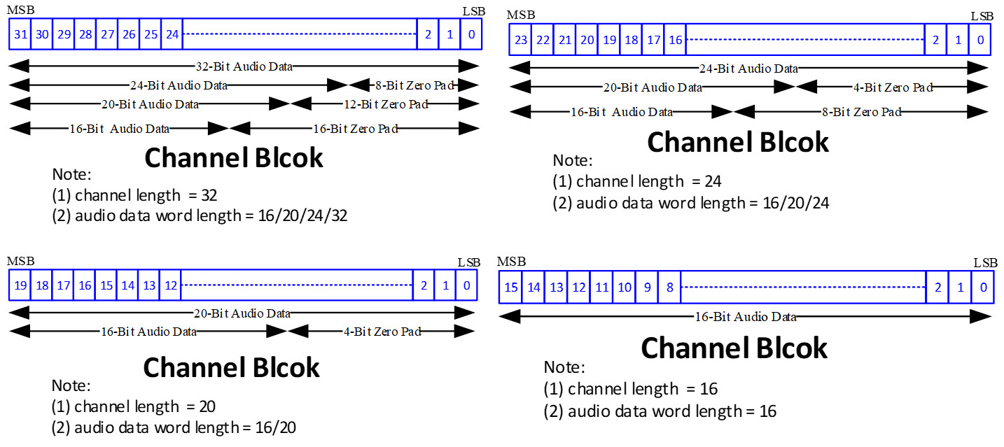
Supports 16/20/24/32 bits data length
Supports 16/20/24/32 bits channel length
Works in master and slave mode.
Supports sampling rate up to 192kHz
Support Multi-IO mode, fs up to 192kHz
General functions
SPORT fs counter and phase counter
SPORT fs counter and phase counter under BCLK
When using phase counter, rx_bclk_div_ratio/ tx_bclk_div_ratio should be configured to
63.Fs counter is used to count the number of LRCLK.
On every falling edge of LRCLK, phase counter would accumulate once in two BCLK cycles by default. On the next falling edge of LRCLK, phase counter will be reset to
0and then start counting again. At this time, the maximum accumulated value of phase counter is31.Phase counter also can accumulate once in one BCLK cycle, the maximum accumulated value of phase counter is
63.SPORT fs and phase counter is shown below:

SPORT fs counter and phase counter under SPORT CLK
SPORT CLK=98.304MHz/45.1584MHz. When the SPORT CLK is 98.304M, and on every rising edge or falling edge of LRCLK, the phase counter will accumulate once in one SPORT clock cycle, the accuracy of phase counter can reach 10ns.
Phase counter can start on the falling edge of LRCLK, and it increments by one at each SPORT CLK. On the next falling edge of LRCLK, phase counter will be reset to
0and then start to count again.Phase counter also can start on the rising edge of LRCLK, the rest is similar to the description above.
In master mode LRCLK is divided by SPORT CLK. In slave mode SPORT LRCLK is supported by master.
SPORT fs counter and phase counter under SPORT CLK is shown below:

Note
N = SPORT CLK/LRCLK
LRCLK start and stop detect: in slave mode, SPORT can use SPORT clock to monitor the start and stop of LRCLK.
Start condition: detect the rising edge or falling edge(default) of LRCLK. The implementation steps are as follows:

Stop condition: the phase counter is accumulated to a settable threshold. The implementation steps are as follows:

SPORT direct mode feature:
Used for data transmission between different sports without CPU and DMA involved in data transfer.
When two sports work in direct mode, clock needs to be at the same frequency.
SPORT FIFO:
TX_FIFO_0 and TX_FIFO_1 are two asynchronous ping-pong FIFO. Each FIFO is
depth=32andwidth=32, so2*32*4 bytes=64 words.RX_FIFO_0 and RX_FIFO_1 are two asynchronous ping-pong FIFO. Each FIFO is
depth=32andwidth=32, so2*32*4 bytes=64 words.6/8 channels for data transmission, FIFO0 and FIFO1 would be used. Two FIFOs will request at the same time, and four SPORTs will produce 16 requests at the same time.
WIFI TSF
WIFI TSF start SPORT

MAC sends interrupt to audio, and hardware will automatically start playing in audio side. The hardware delay is tens of nanoseconds. There is no need to wait for software to set MAC to send interrupt to open the following two bit functions.
((u32)SP0_CTRL0) &= ~ SP_BIT_TX_DISABLE;
((u32)SP0_CTRL0) |= SP_BIT_START_TX;
WIFI TSF latch SPORT counter

Hardware latch SPORT counter when it detects a change in the TSFT specified bit, software specifies the bits. The latch period is optional: 1.024/ 2.048/ 4.096 ……/ 131.072.
SPORT0 is for internal digital microphone interface and external I2S interface
SPORT1 is only for external I2S interface.
Not support LRCLK start and stop detect
Not support SPORT fs counter and phase counter under SPORT CLK
Support WIFI TSF,but not support WIFI TSF start SPORT
SPORT0 is for internal digital microphone interface and external I2S interface
SPORT1 is only for external I2S interface.
Not support LRCLK start and stop detect
Not support SPORT fs counter and phase counter under SPORT CLK
Not support WIFI TSF
SPORT0 is for internal digital microphone interface and external I2S interface
SPORT1 is only for external I2S interface.
Not support LRCLK start and stop detect
Not support SPORT fs counter and phase counter under SPORT CLK
Not support WIFI TSF
SPORT0 is for internal digital microphone interface and external I2S interface
SPORT1 is only for external I2S interface.
Not support LRCLK start and stop detect
Not support SPORT fs counter and phase counter under SPORT CLK
Not support WIFI TSF
SPORT0/1 is for internal audio codec and not support Multi-IO mode.
SPORT2/3 is for external I2S interface. In multi-I/O mode, fs supports up to 384kHz@master TX mode and slave RX mode, and other mode fs supports up to 192KHz.
Not support LRCLK start and stop detect
Not support SPORT fs counter and phase counter under SPORT CLK
Only
CHIP_DCUTsupports WIFI TSF, but not support WIFI TSF start SPORT
I2S Signal Introduction
The I2S bus has three lines:
Continuous serial clock (SCK/BCLK)
One SCK pulse generates a data bit
Master generates SCK
Word select (WS/LRCLK)
The word select line indicates the channel being transmitted:
WS = 0: channel 1 (left)WS = 1: channel 2 (right)
Changes one clock period before the MSB is transmitted
Serial data (SD)
SD is transmitted in two complements with the MSB first. The MSB has a fixed position, whereas the position of the LSB depends on the word length.
When the system word length is greater than the transmitter word length, the word is truncated (the least significant data bits are set to
0).If the receiver is sent more bits than its word length, the bits after the LSB are ignored.
If the receiver is sent fewer bits than its word length, the missing bits are set to zero internally.
I2S Data Format
The I2S interface supports I2S (Philips) format, Left-justified (MSB) format, Right-justified (LSB) format, PCM, and TDM mode. Software can select any mode by setting the I2S control register. The following figures show the I2S data format.
I2S format
Note
Typically, fs = 8/16/32/44.1/48/88.2/96/192/192kHz
Channel length: 16/20/24/32 bits (N+1)
SCK = Arbitrarily cycles within 1/fs, but
>= 2*(N+1) * fs, <= 256 * fs
Left-justified format
Note
Typically, fs = 8/16/32/44.1/48/88.2/96/192/192kHz
Channel length: 16/20/24/32 bits (N+1)
SCK >= 2*(N+1)*fs, <= 256 *fs
PCM mode A
Note
Typically, fs = 8/16/32/44.148/88.2/96/192kHz
Channel length: 16/20/24/32 bits (N+1)
SCK >= 2*(N+1)*fs, <= 256 * fs
PCM mode B
Note
Typically, fs = 8/16/32/44.148/88.2/96/192kHz
Channel length: 16/20/24/32 bits (N+1)
SCK >= 2*(N+1)*fs, <= 256 * fs
I2S TDM 8 mode
Note
Typically, fs = 8/16/32/44.1/48kHz
Channel length: 16/20/24/32 bits (N+1)
SCK >= 8*(N+1)*fs, <= 256 * fs
Left-justified TDM 8 mode
Note
Typically, fs = 8/16/32/44.1/48kHz
Channel length: 16/20/24/32 bits (N+1)
SCK >= 8*(N+1)*fs, <= 256 * fs
PCM mode A in TDM 8 mode
Note
Typically, fs = 8/16/32/44.1/48kHz
Channel length: 16/20/24/32 bits (N+1)
SCK >= 8*(N+1)*fs, <= 256 * fs
PCM mode B in TDM 8 mode
Note
Typically, fs = 8/16/32/44.1/48kHz
Channel length: 16/20/24/32 bits (N+1)
SCK >= 8*(N+1)*fs, <= 256 *fs
I2S TDM 6 mode
Note
Typically, fs = 8/16/32/44.1/48kHz
Channel length: 16/20/24/32 bits (N+1)
SCK >= 6*(N+1)*fs, <= 256 * fs
Left-justified TDM 6 mode
Note
Typically, fs = 8/16/32/44.1/48kHz
Channel length: 16/20/24/32 bits (N+1)
SCK >= 6*(N+1)*fs, <= 256 * fs
PCM mode A in TDM 6 mode
Note
Typically, fs = 8/16/32/44.1/48kHz
Channel length: 16/20/24/32 bits (N+1)
SCK >= 6*(N+1)*fs, <= 256 * fs
PCM mode B in TDM 6 mode
Note
Typically, fs = 8/16/32/44.1/48kHz
Channel length: 16/20/24/32 bits (N+1)
SCK >= 6*(N+1)*fs, <= 256 * fs
I2S TDM 4 mode
Note
Typically, fs = 8/16/32/44.1/48/88.2/96kHz
Channel length: 16/20/24/32 bits (N+1)
SCK >= 4*(N+1)*fs, <= 256 * fs
Left-justified TDM 4 mode
Note
Typically, fs = 8/16/32/44.1/48/88.2/96kHz
Channel length: 16/20/24/32 bits (N+1)
SCK >= 4*(N+1)*fs, <= 256 * fs
PCM mode A in TDM 4 mode
Note
Typically, fs = 8/16/32/44.1/48/88.2/96kHz
Channel length: 16/20/24/32 bits (N+1)
SCK >= 4*(N+1)*fs, <= 256 * fs
PCM mode B in TDM 4 mode
Note
Typically, fs = 8/16/32/44.1/48/88.2/96kHz
Channel length: 16/20/24/32 bits (N+1)
SCK >= 4*(N+1)*fs, <= 256 * fs
I2S supports 16/20/24/32 bits channel length, the relationship between audio data length and channel length is illustrated below.
SPORT Parameters
Interface/Format |
Sampling rate |
Audio bits |
Channel |
Channel length |
BCLK polarity |
Serial data |
Mode |
|---|---|---|---|---|---|---|---|
I2S |
192kHz |
16 bits |
Stereo |
16 bits |
BCLK |
MSB first |
Master |
Left-justified |
96kHz |
20 bits |
Mono |
20 bits |
BCLK inverse |
LSB first |
Slave |
PCM Mode A (Short Frame Sync) |
88.2kHz |
24 bits |
24 bits |
||||
PCM Mode A (Short Frame Sync) |
48kHz |
32 bits |
32 bits |
||||
PCM Mode B (Short Frame Sync) |
44.1kHz |
||||||
PCM Mode B (Short Frame Sync) |
32kHz |
||||||
16kHz |
|||||||
8kHz |
I2S PINMUX
The data PIN DIO[3:0] of I2S can be used as output or input. It can be set as input or output in the corresponding part of I2S in the PAD register. I2S data pinmux is shown below.

The data PIN DIO[3:0] of I2S can be used as output or input. It can be set as input or output in the corresponding part of I2S in the PAD register. I2S data pinmux is shown below.
The data PIN DIO[3:0] of I2S can be used as output or input. It can be set as input or output in the corresponding part of I2S in the PAD register. I2S data pinmux is shown below.
The data PIN DIO[3:0] of I2S can be used as output or input. It can be set as input or output in the corresponding part of I2S in the PAD register. I2S data pinmux is shown below.
The data PIN
DIN[3:0]of I2S is used as input.The data PIN
DOUT[3:0]of I2S is used as output.
Audio Codec
General Description
Audio codec provides 2-channel digital microphone for recording.
The audio codec is a high-performance, up to 4-channel I2S interface audio codec. The transmitted data can be from digital microphone input. Mono high-performance DAC are included.
Two smart digital mic interfaces are supported to make low jitter clock output and decimation filter for up to four digital mics. Independent digital voice controllers are provided in each channel.
PDM interface is supported for PDM digital speaker power amplifier.
An energy-based VAD module is built-in.
The audio codec is a high-performance, up to 4-channel I2S interface audio codec. The transmitted data can be from analog input or digital microphone input. The received data can stream to line output. Three channels analog ADCs and Mono high-performance DAC are included.
Audio codec integrates three ADCs with one mic bias voltage and mic boost amplifier to deliver valid channel data. The analog input port MICIN1_P/N ~ MICIN3_P/N is designed as full differential microphone pins or single-ended line-in pins. Two smart digital mic interfaces are supported to make low jitter clock output and decimation filter for up to four digital mics. Independent digital voice controllers are provided in each channel.
Audio codec integrates mono DAC with different output which actions as an input signal of headset or speaker power amplifier. And also a PDM interface is supported for PDM digital speaker power amplifier.
An energy-based VAD module is built-in.
The audio codec is a high-performance, low-power, up to 8-channel I2S interface audio codec. The transmitted data can be from analog input or digital microphone input. The received data can stream to line output. Five channels analog ADCs can work in low power mode and normal mode. In low power and normal mode, THD+N of five channels ADCs all are about -80dB, and SNR can reach 98dBA. Two high-performance DACs are included, and THD+N of which are all about -85dB, and SNR can reach 98dBA.
Audio codec integrates five ADCs with independent mic bias voltage and mic boost amplifier to deliver valid channel data that channel crosstalk can be eliminated. The analog input port MIC0_P/N ~ MIC4_P/N is designed as full differential microphone pins or single-ended line-in pins. Four smart digital mic interfaces are supported to make low jitter clock output and decimation filter for up to eight digital mics. Independent digital voice controllers are provided in each channel.
Audio codec integrates two DACs with different output which actions as an input signal of headset or speaker power amplifier. And also a PDM interface is supported for PDM digital speaker power amplifier.
Audio codec includes several DSP features such as a high-pass filter, mixer, Equalizer, and volume control. The 10-band parametric Equalizer contains 10 independent filters with programmable gain, center frequency and bandwidth to tailor the frequency characteristics of the embedded playback system according to user preferences. The 5-band parametric Equalizer contains 5 independent filters with programmable gain, center frequency and bandwidth to tailor the frequency characteristics of the embedded record system according to user preferences.
Features
DMIC interface features:
8kHz/11.025kHz/12kHz/16kHz/22.5kHz/24kHz/32kHz/44.1kHz/48kHz/88.2kHz/96kHz for digital microphone interface
Asynchronous sample rate converter (ASRC) for each interface
Configurable 0-5 band EQ
Adjustable digital volume control
For digital volume control, supports zero-crossing detection to minimize audible artifacts
DC remove function
Audio codec features:
8k/11.025k/12k/16k/22.5k/24k/32k/44.1k/48k/88.2k/96kHz for PDM OUT
8k/11.025k/12k/16k/22.5k/24k/32k/44.1k/48k/88.2k/96kHz forDMIC interface
Asynchronous sample rate converter (ASRC) for each interface
For digital volume control, supports zero-crossing detection to minimize audible artifacts
DC remove function for DMIC and PDM.
PDM interface function for external speaker AMP
Audio codec features:
Analog features
DAC with 98dB A-weighted SNR
ADC with 98dB A-weighted SNR
Differential analog microphone inputs with boost pre-amplifiers and low noise microphone bias
0/5/10/15/20/25/30/35/40dB microphone boost gain
MIC input to ADC with 0dB boost gain in low power mode,
SNR > 98dBA-weighted and THD+N is about -80 dB-80dB crosstalk between channels
Adjustable MICBIAS with less than -100dBV noise floor and -70dB PSRR
Mono DAC output with lineout
SNR >= 98dBA-weighted (AVDD=1.8V, load=10kΩ, differential output, 25℃)THD+N is about -85 dB (
AVDD=1.8V, load=10kΩ, differential output, 25℃)Differential output
-80dB crosstalk between channels
Digital features
8k/11.025k/12k/16k/22.5k/24k/32k/44.1k/48k/88.2k/96k/176.4k/192kHz for DAC path
8k/11.025k/12k/16k/22.5k/24k/32k/44.1k/48k/88.2k/96kHz for ADC path
Digital microphone interface supported
Asynchronous sample rate converter (ASRC) for each interface
For digital volume control, supports zero-crossing detection to minimize audible artifacts
DC remove function for ADC, DAC
PDM interface function for external speaker AMP
Audio codec features:
Analog features
DAC with 98dBA SNR
ADC with 98dBA SNR
Differential analog microphone inputs with boost pre-amplifiers and low noise microphone bias
0/5/10/15/20/25/30/35/40dB microphone boost gain
MIC input to ADC with 0dB boost gain in normal mode,
SNR > 98dBAandTHD+N is about -80dBMIC input to ADC with 0dB boost gain in low power mode,
SNR > 90dBAandTHD+N is about -78dB-80dB crosstalk between channels
Adjustable MICBIAS with less than -100dBV noise floor and -70dB PSRR
Dual Stereo DAC outputs with stereo headphone amplifiers
SNR >= 98dBA(AVDD=1.8V,load=10kΩ, dual differential output)THD+N is about -85dB (
AVDD=1.8V,load=10kΩ, dual differential output)Dual differential output
-80dB crosstalk between channels
De-pop function in stereo headphone amplifiers
Digital features
8k/11.025k/12k/16k/22.5k/24k/32k/44.1k/48k/88.2k/96k/176.4k/192kHz for DAC path
8k/11.025k/12k/16k/22.5k/24k/32k/44.1k/48k/88.2k/96kHz for ADC path
Digital microphone interface supported
Asynchronous sample rate converter (ASRC) for each interface
10-bands flexible equalizer (EQ) for DAC path
Configurable 0-5 band EQ in 6 channels for ADC path
Adjustable digital volume control in ADC, DAC
For digital volume control, supports zero-crossing detection to minimize audible artifacts
DC remove function for ADC, DAC
PDM interface function for external speaker AMP
Side tone function
Audio Codec Data Path
Recording Data Path
The following figure shows the recording data path of digital microphone interface. In the recording path, the input source is 2-channel DMIC.

The following figure shows the recording data path of audio codec. In the recording path, the input source can be selected DMIC 0-3, and MUSIC_OUT.
DMIC 0-3 is the data from 4 channel digital microphones.
MUSIC_OUT is the data from DAC SDM out for AEC reference signal.

The following figure shows the recording data path of audio codec. In the recording path, the input source can be selected from ADC 1-3, DMIC 0-3, and MUSIC_OUT.
ADC 1-3 is the data from 3 channel analog ADC
DMIC 0-3 is the data from 4 channel digital microphones.
MUSIC_OUT is the data from DAC SDM out for AEC reference signal.
The following figure shows the recording data path of audio codec. In the recording path, the input source can be selected from ADC 0-4, DMIC 0-7, and MUSIC_OUT.
ADC 0-4 is the data from 5 channel analog ADC
DMIC 0-7 is the data from 8 channel digital microphones.
MUSIC_OUT is the data from DAC SDM out.

Playback Data Path
Not support.
The following figure shows the playback data path of audio codec, which can be SP_L and reference signal.
SP_L is the data from music channel left.
Reference signal is the data from reference signal module for test.

The following figure shows the playback data path of audio codec, which can be SP_L and reference signal.
SP_L is the data from music channel left.
Reference signal is the data from reference signal module for test.

The following figure shows the playback data path of audio codec, which can be SP_L and reference signal.
SP_L is the data from music channel left.
Reference signal is the data from reference signal module for test.
The following figure shows the playback data path of audio codec, which can be SP_L, SP_R, SP_L + SP_R, and reference signal.
SP_Lis the data from music channel left.SP_Ris the data from music channel right.SP_L + SP_Ris the data from music channel left added channel right.Reference signalis the data from reference signal module for test.

Audio Codec Functional Description
Audio codec provides 2-channel digital microphone for recording.
Audio codec provides 1-channel digital interface for PDM.
Audio codec provides 1-channel analog DAC for playback and 3-channel analog ADCs for recording.
Audio codec provides 1-channel analog DAC for playback and 3-channel analog ADCs for recording.
Audio codec provides 2-channel analog DACs for playback and 5-channel analog ADCs for recording.
Audio Recording
Audio Recording Block
The digital microphone (DMIC) interface is for digital microphone, and supports 2-channel digital microphone recording. The following figure shows the details block of digital microphone interface.

There are 4 channel digital microphone interface for digital microphone recording application.

There are three analog ADCs and with up to 3-channel recording paths. You can use three microphones to pass to analog ADCs. Three-channel ADCs has two type analog input ports: microphone input and line input, which all support differential and single end.
The IN1-3P/N are microphone-type input ports. The input port can be configured to differential input or single-ended input. The microphone input port has its microphone bias and microphone boost. The low noise microphone bias can improve recording performance and enhance recording quality. Built-in short current detection scheme can be used for switch detection. Multi-step microphone boost gain is easy to use for microphone applications. The following figure shows the recording analog block.
A boost amplifier is provided in the input path to the ADC, which can be used manually with 5dB step from 0dB to 40dB, to keep the recording volume constant.

Analog and digital MIC recording path
The recording part includes one programmable microphone bias output, capable of providing output voltages of 1.8V with 3mA output-current drive capability. It can be powered down completely when not needed for power saving. The following figure shows the function block of MICBIAS.

There are three analog ADCs and with up to 3-channel recording paths. You can use three microphones to pass to analog ADCs. Three-channel ADCs has two type analog input ports: microphone input and line input, which all support differential and single end.
The IN1-3P/N are microphone-type input ports. The input port can be configured to differential input or single-ended input. The microphone input port has its microphone bias and microphone boost. The low noise microphone bias can improve recording performance and enhance recording quality. Built-in short current detection scheme can be used for switch detection. Multi-step microphone boost gain is easy to use for microphone applications. The following figure shows the recording analog block.
A boost amplifier is provided in the input path to the ADC, which can be used manually with 5dB step from 0dB to 40dB, to keep the recording volume constant.
Analog and digital MIC recording path
The recording part includes one programmable microphone bias output, capable of providing output voltages of 1.8V with 3mA output-current drive capability. It can be powered down completely when not needed for power saving. The following figure shows the function block of MICBIAS.
There are five analog ADCs and with up to 5-channel recording paths. You can use five microphones to pass to analog ADCs. Five channel ADCs has two type analog input ports: microphone input and line input, which all support differential and single-ended.
The IN0-4P/N are microphone-type input ports. The input port can be configured to differential input or single-ended input. The microphone input port has its microphone bias and microphone boost. The low noise microphone bias can improve recording performance and enhance recording quality. Build-in short current detection scheme can be used for switch detection. Multi-step microphone boost gain is easy to use for microphone applications. The following figure shows the recording analog block.
A boost amplifier is provided in the input path to the ADC, which can be used manually with 5dB step from 0dB to 40dB, to keep the recording volume constant.
There are up to 8-channel digital microphone interface which shares the digital path with AMIC ADC.

Analog and digital MIC recording path
The recording part includes five programmable microphone bias outputs (MICBIAS0, MICBIAS1, MICBIAS2, MICBIAS3, MICBIAS4), capable of providing output voltages of 1.8V with 3mA output-current drive capability. In addition, the MICBIAS outputs may be programmed to be switched to AVCC_DRV directly through an on-chip switch, and it can be powered down completely when no need for power saving. The following figure shows the function block of MICBIAS.

Note
In low power mode, the power supply of external AMIC should be switched to AVCC_DRV. You can configure GPIO<16:12> to output HIGH to realize it. This is equivalent to that the phase inverter outputs high level, and software conduction resistance is about 33Ω.
Digital Feature of Audio Recording
Recording path for sampling rate 8k/11.025k/12k/16k/32k/22.05k/44.1k/48k/88.2k/96kHz
ASRC (asynchronous sample rate converter)
The ADC digital part supports digital volume control, and the gain is between 48dB and -17.625dB in 0.375dB per step.
There is a high pass filter for DC offset
Zero-crossing function
If the volume is adjusted while the signal is a non-zero value, an audible click can occur, as shown below.
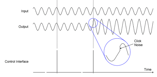
Click noise without zero crossing
In order to prevent this click noise, a zero-crossing function is provided. When enabled, this will cause the volume to update only when a zero crossing occurs, minimizing click noise, as shown below.
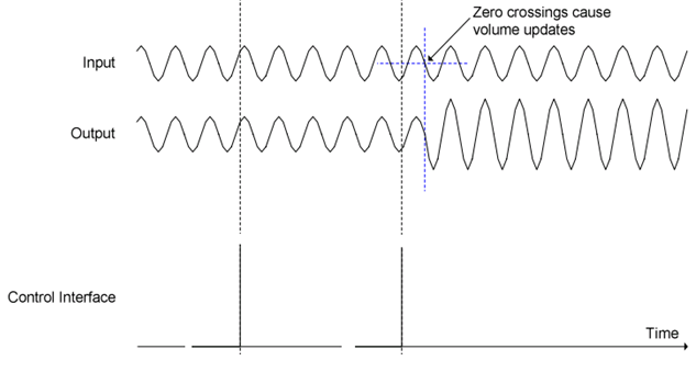
Minimizing click noise with zero crossing
When the signal is very quiet and consists of mainly of noise, zero crossing cannot be met, now the gain will change with steps, as shown below.
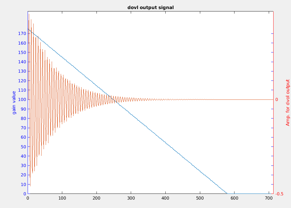
Gain update with steps as zero crossing
Equalizer block
The equalizer block cascades 0-5 bands of equalizer to tailor the frequency characteristics of the recording system according to user preferences and to emulate environment sound.
DC remove function block
A high pass filter is implemented for dc offset. The high pass filter is mainly for ADC recording used. The cut-off frequency of filter is programmable and is varied according to different sample rates. The filter is used to remove DC offset at normal conditions.
Silence detector block
The Silence detector is used to reduce the noise floor for DAC path or ADC path. When the input signal is below silence level, the input signal will be reduced to suppress the background noise. The reducing level can be set by registers.
Not support equalizer block.
Not support equalizer block.
Not support equalizer block.
Audio Playback
Not support.
Build-in 1-channel PDM out interface, connected to a PDM speaker amplifier to playback.
Build-in 1-channel sigma-delta DAC is an on-chip Sigma-Delta Modulator, and a 24-bit input high-performance current steering DAC is composed of it. The analog part controls the current cell by the signal from digital part, and changes digital signal to analog signal and sends to Power Amplifier (PA).
Build-in 1-channel sigma-delta DAC is an on-chip Sigma-Delta Modulator, and a 24-bit input high-performance current steering DAC is composed of it. The analog part controls the current cell by the signal from digital part, and changes digital signal to analog signal and sends to Power Amplifier (PA).
Build-in 2-channel sigma-delta DAC is an on-chip Sigma-Delta Modulator, and a 24-bit input high-performance current steering DAC is composed of it. The analog part controls the current cell by the signal from digital part, and changes digital signal to analog signal and sents to Power Amplifier (PA).
Audio Playback Block
Not support.
Built-in a PDM interface, for PDM speaker amplifier, the interface will support mono speaker.

Built-in high-performance stereo current steering DAC, and with stereo headphone driver amplifiers, the amplifiers support differential output and an anti-pop circuit can suppress the noise of amplifier when power up effectively. The headphone driver amplifiers include 4 level volume control, which decreases 3dB by one step. LOUT signal is from DAC_L.

Built-in a PDM interface, for PDM speaker amplifier, the interface will support mono speaker.
Built-in high-performance stereo current steering DAC, and with stereo headphone driver amplifiers, the amplifiers support differential output and an anti-pop circuit can suppress the noise of amplifier when power up effectively. The headphone driver amplifiers include 4 level volume control, which decreases 3dB by one step. LOUT signal is from DAC_L.
Built-in a PDM interface, for PDM speaker amplifier, the interface will support mono speaker.
Built-in high-performance stereo current steering DAC, and with stereo headphone driver amplifiers, the amplifiers support differential output and an anti-pop circuit can suppress the noise of amplifier when power up effectively. The headphone driver amplifiers include 4 level volume control, which decreases 3dB by one step. LOUT signal is from DAC_L and ROUT signal is from DAC_R.

Analog of audio playback block
Built-in a PDM interface, for PDM speaker amplifier, the interface will support stereo speaker.
Digital Feature of Audio Playback
Not support.
Playback path for sample rate 8K,11.025K,12K,16K,32K,22.05K,44.1K 48kHz,88.2K,96kHz, 176.4K,192K
ASRC supports up to 96kHZ sample rate
The DAC digital part support digital volume control, and the gain is between 0dB and -65.625dB in 0.375dB/step.
There is a high pass filter for DC offset, the cut-off frequency of filter is programmable and is varied according to different sample rates.
Zero crossing function, this function is the same as ADC zero crossing.
Silence detector block
The Silence detector is used to reduce the noise floor for DAC path or ADC path. When the input signal is below silence level, the input signal will be reduced to suppress the background noise. The reducing level can be set by registers.
PDM interface
Test tone
Built-in a test tone module, the tone frequency can be configured by
(fs/192)*(tone_fc_sel+1)kHz, and the tone gain can be configured by0 ~ 6.02*(gain_sel)dB.
Playback path for sample rate 8K,11.025K,12K,16K,32K,22.05K,44.1K 48kHz,88.2K,96kHz, 176.4K,192K
Asynchronous Sample Rate Converters (ASRC)
The DAC digital part support digital volume control, and the gain is between 0dB and -65.625dB in 0.375dB per step.
There is a high pass filter for DC offset, the cut-off frequency of filter is programmable and is varied according to different sample rates.
Zero-crossing function, which is the same as ADC zero-crossing.
PDM interface
Test tone
Built-in a test tone module, the tone frequency can be configured by
(fs/192) * (tone_fc_sel+1) kHz, and the tone gain can be configured by0 ~ 6.02 * (gain_sel) dBChannel L and channel R mix
Before streaming to DAC, channel L data and channel R data are mixed, then streamed to DAC_L channel and DAC_R channel.
VAD_PITCH
VAD_PITCH Features
VAD (Voice Activity Detection) is a low-energy voice detect IP. It supports voice trigger. Once the VAD function is enabled, it will automatically sample the voice and detect the voice energy above the threshold value or not, even the processor is in sleep mode.
The overall design of VAD mainly includes two aspects, one is the generation of wake-up interrupt, to wake up the processor; the other is the transmission of voice data after wake-up, to let the processor timely access to audio data for keyword recognition.
VAD data source may be up to four analog microphones, and up to eight digital microphones. The VAD can configure software to choose which audio source to use as input. An APB configuration interface is also supported. When the VAD successfully recognizes a human voice in CPU low power mode, an interrupt is generated and reported to the CPU.
SRAM is used to store audio data buffer during power consumption. It is 128KB in size and supports 64 bits read/write. The data source is parallel to the VAD’s audio data source and is also audio data after the MUX.
At the same time, SRAM can also be read and written by KM0, KM4 and CA32 at workflow.
Not support VAD_PITCH
Not support VAD_PITCH
Not support VAD_PITCH
Not support VAD_PITCH
Support VAD_PITCH
Register
SPORT Register
Base Address:
SPORT0_REG : 0x4012A000
SPORT1_REG : 0x4012B000
Name |
Address offset |
Access |
Description |
|---|---|---|---|
000h |
R/W |
||
004h |
R/W |
||
008h |
R/W |
||
00Ch |
R/W |
||
014h |
R |
||
018h |
R |
||
01Ch |
R/W |
||
020h |
R/W |
||
024h |
R |
||
028h |
R/W |
||
02Ch |
R/W |
||
030h |
R/W |
||
034h |
R |
||
03Ch |
R/W |
||
044h |
R/W |
||
048h |
R/W |
||
04Ch |
R/W |
||
054h |
R/W |
||
058h |
R/W |
||
05Ch |
R/W |
||
060h |
R |
||
064h |
R/W |
||
800h |
R/W |
||
880h |
R |
||
900h |
R/W |
||
980h |
R |
REG_SP_REG_MUX
Name : SPORT MUX Register
Size : 32
Address offset : 000h
Read/write access : R/W
Bit |
Symbol |
Access |
Reset |
Description |
|---|---|---|---|---|
31:0 |
SP_REG_MUX |
R/W |
0xFFFFFFFF |
Mux of register write with different base address of the sam e SPORT. This field can be set as different value with four different base address in one SPORT, but other registers share the sam e value with four different base address in one SPORT. |
REG_SP_CTRL0
Name : SPORT Control Register 0
Size : 32
Address offset : 004h
Read/write access : R/W
Bit |
Symbol |
Access |
Reset |
Description |
|---|---|---|---|---|
31:30 |
MCLK_SEL |
R/W |
0x0 |
Not used, refer to 0x64 2’b00: MCLK output=dsp_src_clk/4 2’b01: MCLK output=dsp_src_clk/2 2’b10/2’b11: MCLK output=dsp_src_clk |
29:28 |
SP_SEL_I2S_RX_CH |
R/W |
0x0 |
2’b00: L/R 2’b01: R/L 2’b10: L/L 2’b11: R/R x ADC path |
27:26 |
SP_SEL_I2S_TX_CH |
R/W |
0x0 |
2’b00: L/R 2’b01: R/L 2’b10: L/L 2’b11: R/R x DAC path |
25 |
SP_START_RX |
R/W |
0 |
1’b0: Rx is disabled 1’b1: Rx is started |
24 |
SP_RX_DISABLE |
R/W |
1 |
1’b1: SPORT Rx is disabled. 1’b0: SPORT Rx is enabled. |
23 |
RX_LSB_FIRST_0 |
R/W |
0 |
1’b0: MSB first when Rx 1’b1: LSB first |
22 |
TX_LSB_FIRST_0 |
R/W |
0 |
1’b0: MSB first when Tx 1’b1: LSB first |
21:20 |
SP_TDM_MODE_SEL_RX |
R/W |
0x0 |
2’b00: Without TDM 2’b01: TDM4 2’b10: TDM6 2’b11: TDM8 |
19:18 |
SP_TDM_MODE_SEL_TX |
R/W |
0x0 |
2’b00: Without TDM 2’b01: TDM4 2’b10: TDM6 2’b11: TDM8 |
17 |
SP_START_TX |
R/W |
0 |
1’b0: Tx is disabled. 1’b1: Tx is started. |
16 |
SP_TX_DISABLE |
R/W |
1 |
1’b1: SPORT Tx is disabled. 1’b0: SPORT Tx is enabled. |
15 |
SP_I2S_SELF_LPBK_EN |
R/W |
0 |
1’b1: internal loopback mode is enabled |
14:12 |
SP_DATA_LEN_SEL_TX_0 |
R/W |
0x0 |
3’b000: 16 bits 3’b001: 20 bits 3’b010: 24 bits 3’b100: 32 bits |
11 |
SP_EN_I2S_MONO_TX_0 |
R/W |
0 |
1’b1: mono 1’b0: stereo |
10 |
SP_INV_I2S_SCLK |
R/W |
0 |
1’b1: I2S/PCM bit clock is inverted |
9:8 |
SP_DATA_FORMAT_SEL_TX |
R/W |
0x0 |
2’b00: I2S 2’b01: Left-justified 2’b10: PCM mode A 2’b11: PCM mode B |
7 |
DSP_CTL_MODE |
R/W |
0 |
1’b1: DSP and SPORT1 handshaking is enabled. 1’b0: GDMA and SPORT1 handshaking is enabled. |
6 |
SP_LOOPBACK |
R/W |
0 |
1’b1: self-loopback mode |
5 |
SP_WCLK_TX_INVERSE |
R/W |
0 |
1’b1: I2S/PCM word clock is inverted for Tx (SPK path) |
4 |
SLAVE_DATA_SEL |
R/W |
0 |
1’b1: To be an I2S or PCM slave (data path) |
3 |
SLAVE_CLK_SEL |
R/W |
0 |
1’b1: To be an I2S or PCM slave (CLK path) |
2 |
RX_INV_I2S_SCLK |
R/W |
0 |
|
1 |
TX_INV_I2S_SCLK |
R/W |
0 |
|
0 |
SP_RESET |
R/W |
0 |
1’b1: reset SPORT1 module, and remember to write “1” to rese t and then write “0” to release from reset. |
REG_SP_CTRL1
Name : SPORT Control Register 1
Size : 32
Address offset : 008h
Read/write access : R/W
Bit |
Symbol |
Access |
Reset |
Description |
|---|---|---|---|---|
31 |
RX_FIFO_1_REG_1_EN |
R/W |
0 |
1’b1: Enable last two channels of RX_FIFO_1. Only enable whe n RX_FIFO_1_REG_1_EN = 1. |
30 |
RX_FIFO_1_REG_0_EN |
R/W |
0 |
1’b1: Enable first two channels of RX_FIFO_1. Only enable wh en RX_FIFO_0_REG_0_EN = 1. |
29 |
RX_FIFO_0_REG_1_EN |
R/W |
0 |
1’b1: Enable last two channels of RX_FIFO_0. Only enable whe n RX_FIFO_0_REG_0_EN = 1. |
28 |
RX_FIFO_0_REG_0_EN |
R/W |
1 |
1’b1: Enable first two channels of RX_FIFO_0. Disable 0x0008 [28] ~ Disable 0x0008[31] at the same time to reset Rx FIFO. |
27 |
TX_FIFO_1_REG_1_EN |
R/W |
0 |
1’b1: Enable last two channels of TX_FIFO_1. Only enable whe n TX_FIFO_1_REG_0_EN = 1. |
26 |
TX_FIFO_1_REG_0_EN |
R/W |
0 |
1’b1: Enable first two channels of TX_FIFO_1. Only enable wh en TX_FIFO_0_REG_0_EN = 1. |
25 |
TX_FIFO_0_REG_1_EN |
R/W |
0 |
1’b1: Enable last two channels of TX_FIFO_0. Only enable whe n TX_FIFO_0_REG_0_EN = 1. |
24 |
TX_FIFO_0_REG_0_EN |
R/W |
1 |
1’b1: Enable first two channels of TX_FIFO_0. Disable 0x0008 [24] ~ Disable 0x0008[27] at the same time to reset Tx FIFO. |
23 |
RX_SNK_LR_SWAP_0 |
R/W |
0 |
1’b1: swap L/R audio samples written to the sink memory of R X_FIFO_0 |
22 |
RX_SNK_BYTE_SWAP_0 |
R/W |
0 |
1’b1: swap H/L bytes written to the sink memory of RX_FIFO_0 |
21 |
TX_SRC_LR_SWAP_0 |
R/W |
0 |
1’b1: swap L/R audio samples read from the source memory of TX_FIFO_0 |
20 |
TX_SRC_BYTE_SWAP_0 |
R/W |
0 |
1’b1: swap H/L bytes read from the source memory of TX_FIFO_ 0 |
19 |
DIRECT_MODE_EN |
R/W |
0 |
1’b1: WS (LRCK) and SCK (BCLK) are from other SPORT |
18:17 |
SP_DIRECT_SRC_SEL |
R/W |
0x0 |
2’b00: WS and SCK are from SPORT0. 2’b01: WS and SCK are from SPORT1. 2’b10: WS and SCK are from SPORT2. 2’b11: WS and SCK are from SPORT3. |
16 |
ERR_CNT_SAT_SET |
R/W |
0 |
1’b1: saturation count (65534 -> 65535 -> 65535 …) 1’b0: wrap count (65534 -> 65535 -> 0 -> 1 -> 2 …) |
15:14 |
SPORT_CLK_SEL |
R/W |
0x0 |
2’b0x00: dsp_src_clk (BCLK*2) 2’b10: dsp_src_clk (BCLK*4)/2 2’b11: dsp_src_clk (BCLK*8)/4 |
13 |
CLEAR_RX_ERR_CNT |
R/W |
0 |
Write 1’b1 and then write 0 to clear Rx error counter |
12 |
CLEAR_TX_ERR_CNT |
R/W |
0 |
Write 1’b1 and then write 0 to clear Tx error counter |
11 |
ENABLE_MCLK |
R/W |
0 |
Enable mclk. |
10:8 |
DEBUG_BUS_SEL |
R/W |
0x0 |
3’b000: debug_bus_a 3’b001: debug_bus_b … 3’b111: debug_bus_h |
7 |
WS_FORCE_VAL |
R/W |
1 |
When WS_FORCE = 1, ws_out_tx and ws_out_rx = “ws_force_val” |
6 |
WS_FORCE |
R/W |
0 |
|
5 |
BCLK_RESET |
R/W |
0 |
1’b0: Enable bclk 1’b1: Disable and reset bclk |
4 |
BCLK_PULL_ZERO |
R/W |
0 |
Write 1’b1 to pull bclk to 0 smoothly Write 1’b0 to reopen bclk |
3 |
MULTI_IO_EN_RX |
R/W |
1 |
1’b1: Enable multi-IO of Rx 1’b0: Disable multi-IO of Rx |
2 |
MULTI_IO_EN_TX |
R/W |
1 |
1’b1: Enable multi-IO of Tx 1’b0: Disable multi-IO of Tx |
1 |
TX_FIFO_FILL_ZERO |
R/W |
0 |
X is the burst size of TX_FIFO_0. Y is the burst size of TX_ FIFO_1. Fill TX_FIFO_0 with X zero data and fill TX_FIFO_1 with Y ze ro data. This control bit is “write 1 clear” type |
0 |
SP_RESET_SMOOTH |
R/W |
0 |
1’b1: reset SPORT1 module with complete LRCK cycle. |
REG_SP_INT_CTRL
Name : SPORT Interrupt Control Register
Size : 32
Address offset : 00Ch
Read/write access : R/W
Bit |
Symbol |
Access |
Reset |
Description |
|---|---|---|---|---|
31:24 |
INT_ENABLE_DSP_1 |
R/W |
0x0 |
Bit[24]: for the interrupt of “sp_ready_to_tx_1” Bit[25]: for the interrupt of “sp_ready_to_rx_1” Bit[26]: for the interrupt of “tx_fifo_full_intr_1” Bit[27]: for the interrupt of “rx_fifo_full_intr_1” Bit[28]: for the interrupt of “tx_fifo_empty_intr_1” Bit[29]: for the interrupt of “rx_fifo_empty_intr_1” Bit[30]: for the interrupt of “tx_i2s_idle_1” Bit[31]: Reserved |
23:16 |
INT_ENABLE_DSP_0 |
R/W |
0x0 |
Bit[16]: for the interrupt of “sp_ready_to_tx” Bit[17]: for the interrupt of “sp_ready_to_rx” Bit[18]: for the interrupt of “tx_fifo_full_intr” Bit[19]: for the interrupt of “rx_fifo_full_intr” Bit[20]: for the interrupt of “tx_fifo_empty_intr” Bit[21]: for the interrupt of “rx_fifo_empty_intr” Bit[22]: for the interrupt of “tx_i2s_idle” Bit[23]: Reserved |
15:14 |
DUMMY |
R/W |
0x0 |
- |
13:9 |
INTR_CLR_1 |
R/W |
0x0 |
Bit[9]: for the interrupt of “tx_fifo_full_intr_1” Bit[10]: for the interrupt of “rx_fifo_full_intr_1” Bit[11]: for the interrupt of “tx_fifo_empty_intr_1” Bit[12]: for the interrupt of “rx_fifo_empty_intr_1” Bit[13]: Reserved |
8 |
RX_DSP_CLEAR_INT_1 |
R/W |
0 |
For DSP mode (bypass GDMA), F/W writes 1’b1 and then 1’b0 to clear Rx interrupt. Note Rx interrupt is to indicate that DSP can get audio data f rom RX_FIFO_1. |
7 |
TX_DSP_CLEAR_INT_1 |
R/W |
0 |
For DSP mode (bypass GDMA), F/W writes 1’b1 and then 1’b0 to clear TX interrupt. Note Tx interrupt is to indicate that DSP can write audio data to TX_FIFO_1. |
6:2 |
INTR_CLR_0 |
R/W |
0x0 |
Bit[2]: for the interrupt of “tx_fifo_full_intr” Bit[3]: for the interrupt of “rx_fifo_full_intr” Bit[4]: for the interrupt of “tx_fifo_empty_intr” Bit[5]: for the interrupt of “rx_fifo_empty_intr” Bit[6]: Reserved |
1 |
RX_DSP_CLEAR_INT_0 |
R/W |
0 |
For DSP mode (bypass GDMA), F/W writes 1’b1 and then 1’b0 to clear Rx interrupt. Note Rx interrupt is to indicate that DSP can get audio data f rom RX_FIFO_0. |
0 |
TX_DSP_CLEAR_INT_0 |
R/W |
0 |
For DSP mode (bypass GDMA), F/W writes 1’b1 and then 1’b0 to clear Tx interrupt. Note Tx interrupt is to indicate that DSP can write audio data to TX_FIFO_0. |
REG_SP_TRX_COUNTER_STATUS
Name : SPORT TRX Counter Status Register
Size : 32
Address offset : 014h
Read/write access : R
Bit |
Symbol |
Access |
Reset |
Description |
|---|---|---|---|---|
31 |
SP_RESET_STATE |
R |
0 |
1’b1: sp_reset is enabled. 1’b0: sp_reset is disabled. |
30 |
RSVD |
R |
- |
Reserved |
29:24 |
RX_DEPTH_CNT_1 |
R |
0x0 |
RX_FIFO_1 depth counter status (MIC path) |
23:22 |
RSVD |
R |
- |
Reserved |
21:16 |
TX_DEPTH_CNT_1 |
R |
0x0 |
TX_FIFO_1 depth counter status (SPK path) |
15:14 |
RSVD |
R |
- |
Reserved |
13:8 |
RX_DEPTH_CNT_0 |
R |
0x0 |
RX_FIFO_0 depth counter status (MIC path) |
7:6 |
RSVD |
R |
- |
Reserved |
5:0 |
TX_DEPTH_CNT_0 |
R |
0x0 |
TX_FIFO_0 depth counter status (SPK path) |
REG_SP_ERR
Name : SPORT Error Register
Size : 32
Address offset : 018h
Read/write access : R
Bit |
Symbol |
Access |
Reset |
Description |
|---|---|---|---|---|
31:16 |
RX_ERR_CNT |
R |
0x0 |
Rx error counter (MIC path) Note This counter should always be zero if everything works we ll. |
15:0 |
TX_ERR_CNT |
R |
0x0 |
Tx error counter (SPK path) Note This counter should always be zero if everything works we ll. |
REG_SR_TX_BCLK
Name : SPORT Tx BCLK Register
Size : 32
Address offset : 01Ch
Read/write access : R/W
Bit |
Symbol |
Access |
Reset |
Description |
|---|---|---|---|---|
31 |
TX_MI_NI_UPDATE |
R/W |
0 |
1’b1: to update “mi” and “ni” to get the new clock rate. This bit will be reset automatically when the update is done |
30:16 |
TX_NI |
R/W |
0x30 |
BCLK = 40MHz*(ni/mi) For example: BCLK=3.072MHz=40MHz*(48/625) |
15:0 |
TX_MI |
R/W |
0x271 |
REG_SP_TX_LRCLK
Name : SPORT Tx LRCLK Register
Size : 32
Address offset : 020h
Read/write access : R/W
Bit |
Symbol |
Access |
Reset |
Description |
|---|---|---|---|---|
31:24 |
RX_BCLK_DIV_RATIO |
R/W |
0x3F |
Rx bclk even-bit integer divider. Used in “mode_40mhz” set as 1’b1. (rx_bclk_div_ratio + 1) is the number of “sck_out” cycles wi thin a “ws_out_rx” cycle (1/fs). Default of (rx_bclk_div_ratio + 1) is 64. Set as 64 – 1 = 63 . Only odd number supported. Maximum is 255. |
23:16 |
TX_BCLK_DIV_RATIO |
R/W |
0x3F |
Tx bclk even-bit integer divider. Used in “mode_40mhz” set as 1’b1. (tx_bclk_div_ratio + 1) is the number of “sck_out” cycles wi thin a “ws_out_tx” cycle (1/fs). Default of (tx_bclk_div_ratio + 1) is 64. Set as 64 – 1 = 63 . Only odd number supported. Maximum is 255. |
15:14 |
DUMMY1 |
R/W |
0x0 |
- |
13:8 |
RXDMA_BUSRTSIZE |
R/W |
0x10 |
Rx DMA burst size |
7:6 |
DUMMY2 |
R/W |
0x0 |
- |
5:0 |
TXDMA_BURSTSIZE |
R/W |
0x10 |
Tx DMA burst size |
REG_SP_FIFO_CTRL
Name : SPORT FIFO Control Register
Size : 32
Address offset : 024h
Read/write access : R
Bit |
Symbol |
Access |
Reset |
Description |
|---|---|---|---|---|
31 |
RX_FIFO_EMPTY_0 |
R |
1 |
|
30 |
TX_FIFO_EMPTY_0 |
R |
1 |
|
29 |
RX_FIFO_FULL_0 |
R |
0 |
|
28 |
TX_FIFO_FULL_0 |
R |
0 |
|
27 |
RX_FIFO_EMPTY_1 |
R |
1 |
|
26 |
TX_FIFO_EMPTY_1 |
R |
1 |
|
25 |
RX_FIFO_FULL_1 |
R |
0 |
|
24 |
TX_FIFO_FULL_1 |
R |
0 |
|
23:14 |
RSVD |
R |
- |
Reserved |
13 |
TX_I2S_IDLE_1 |
R |
0 |
|
12 |
RX_FIFO_EMPTY_INTR_1 |
R |
0 |
|
11 |
TX_FIFO_EMPTY_INTR_1 |
R |
0 |
|
10 |
RX_FIFO_FULL_INTR_1 |
R |
0 |
|
9 |
TX_FIFO_FULL_INTR_1 |
R |
0 |
|
8 |
SP_READY_TO_RX_1 |
R |
0 |
|
7 |
SP_READY_TO_TX_1 |
R |
0 |
|
6 |
TX_I2S_IDLE_0 |
R |
0 |
|
5 |
RX_FIFO_EMPTY_INTR_0 |
R |
0 |
|
4 |
TX_FIFO_EMPTY_INTR_0 |
R |
0 |
|
3 |
RX_FIFO_FULL_INTR_0 |
R |
0 |
|
2 |
TX_FIFO_FULL_INTR_0 |
R |
0 |
|
1 |
SP_READY_TO_RX_0 |
R |
0 |
|
0 |
SP_READY_TO_TX_0 |
R |
0 |
|
REG_SP_FORMAT
Name : SPORT Format Register
Size : 32
Address offset : 028h
Read/write access : R/W
Bit |
Symbol |
Access |
Reset |
Description |
|---|---|---|---|---|
31 |
TRX_SAME_CH_LEN |
R/W |
0 |
|
30:28 |
SP_CH_LEN_SEL_RX |
R/W |
0x4 |
3’b000: 16 bits 3’b001: 20 bits 3’b010: 24 bits 3’b100: 32 bits |
27 |
DUMMY3 |
R/W |
0 |
- |
26:24 |
SP_CH_LEN_SEL_TX |
R/W |
0x4 |
3’b000: 16 bits 3’b001: 20 bits 3’b010: 24 bits 3’b100: 32 bits |
23 |
RX_IDEAL_LEN_EN |
R/W |
0 |
Function enable of rx_ideal_len. |
22:20 |
RX_IDEAL_LEN |
R/W |
0x0 |
Sd_in can be received 1 ~ 8 ( = rx_ideal_len + 1 ) BCLK cycl e latter. |
19 |
TX_IDEAL_LEN_EN |
R/W |
0 |
Function enable of tx_ideal_len. PCMA SDO will be delayed 1 LRCK. |
18:16 |
TX_IDEAL_LEN |
R/W |
0x0 |
Sd_out can be sent 1 ~ 8 ( = tx_ideal_len + 1 ) BCLK cycle e arlier. |
15 |
DUMMY4 |
R/W |
0 |
- |
14:12 |
SP_DATA_LEN_SEL_RX_0 |
R/W |
0x0 |
Data length of MIC path and it is valid if “trx_same_length” == 1’b0. 3’b000: 16 bits 3’b001: 20 bits 3’b010: 24 bits 3’b100: 32 bits |
11 |
SP_EN_I2S_MONO_RX_0 |
R/W |
0 |
Channel format of MIC path and it is valid if “trx_same_ch” == 1’b0.
|
10 |
TRX_SAME_LRC |
R/W |
0 |
|
9:8 |
SP_DATA_FORMAT_SEL_RX |
R/W |
0x0 |
Data format of MIC path and it is valid if “trx_same_fs” == 1’b0. 2’b00: I2S 2’b01: Left-justified 2’b10: PCM mode A 2’b11: PCM mode B |
7 |
FIXED_BCLK |
R/W |
0 |
|
6 |
FIXED_BCLK_SEL |
R/W |
0 |
|
5 |
SP_WCLK_RX_INVERSE |
R/W |
0 |
|
4 |
DUMMY5 |
R/W |
0 |
- |
3 |
SCK_OUT_INVERSE |
R/W |
0 |
|
2 |
TRX_SAME_LENGTH |
R/W |
1 |
Both are either 16 or 24 bits |
1 |
TRX_SAME_CH |
R/W |
1 |
Both are either stereo or mono |
0 |
TRX_SAME_FS |
R/W |
1 |
|
REG_SP_RX_BCLK
Name : SPORT Rx BCLK Register
Size : 32
Address offset : 02Ch
Read/write access : R/W
Bit |
Symbol |
Access |
Reset |
Description |
|---|---|---|---|---|
31 |
RX_MI_NI_UPDATE |
R/W |
0 |
1’b1: to update “mi” and “ni” to get the new clock rate. This bit will be reset automatically when the update is done |
30:16 |
RX_NI |
R/W |
0x30 |
BCLK = 40MHz*(ni/mi) For example: BCLK=3.072MHz=40MHz*(48/625) |
15:0 |
RX_MI |
R/W |
0x271 |
REG_SP_RX_LRCLK
Name : SPORT Rx LRCLK Register
Size : 32
Address offset : 030h
Read/write access : R/W
Bit |
Symbol |
Access |
Reset |
Description |
|---|---|---|---|---|
31 |
CLR_TX_SPORT_RDY |
R/W |
0 |
For read, the read data is from clr_tx_sport_rdy |
30 |
EN_TX_SPORT_INTERRUPT |
R/W |
0 |
Enable tx_sport_interrupt |
29 |
EN_FS_PHASE_LATCH |
R/W |
0 |
This control bit is “write 1 clear” type |
28:27 |
DUMMY6 |
R/W |
0x0 |
|
26:0 |
TX_SPORT_COMPARE_VAL |
R/W |
0x40 |
X = (tx_sport_compare_val). When counter equal X. SPORT will send tx_sport_interrupt to DSP. FW should take care X={32~134217727} |
REG_SP_DSP_COUNTER
Name : SPORT DSP Counter Register
Size : 32
Address offset : 034h
Read/write access : R
Bit |
Symbol |
Access |
Reset |
Description |
|---|---|---|---|---|
31:5 |
TX_SPORT_COUNTER |
R |
0x0 |
For DSP read instant Tx SPORT counter value, counter down |
4:0 |
TX_FS_PHASE_RPT |
R |
0x0 |
Report Tx phase |
REG_SP_DIRECT_CTRL0
Name : SPORT Direct Control Register 0
Size : 32
Address offset : 03Ch
Read/write access : R/W
Bit |
Symbol |
Access |
Reset |
Description |
|---|---|---|---|---|
31:28 |
TX_CH7_DATA_SEL |
R/W |
0x7 |
4’h0: tx_fifo_0_reg_0_l 4’h1: tx_fifo_0_reg_0_r 4’h2: tx_fifo_0_reg_1_l 4’h3: tx_fifo_0_reg_1_r 4’h4: tx_fifo_1_reg_0_l 4’h5: tx_fifo_1_reg_0_r 4’h6: tx_fifo_1_reg_1_l 4’h7: tx_fifo_1_reg_1_r 4’h8: direct_reg_7 |
27:24 |
TX_CH6_DATA_SEL |
R/W |
0x6 |
4’h8: direct_reg_6 |
23:20 |
TX_CH5_DATA_SEL |
R/W |
0x5 |
4’h8: direct_reg_5 |
19:16 |
TX_CH4_DATA_SEL |
R/W |
0x4 |
4’h8: direct_reg_4 |
15:12 |
TX_CH3_DATA_SEL |
R/W |
0x3 |
4’h8: direct_reg_3 |
11:8 |
TX_CH2_DATA_SEL |
R/W |
0x2 |
4’h8: direct_reg_2 |
7:4 |
TX_CH1_DATA_SEL |
R/W |
0x1 |
4’h8: direct_reg_1 |
3:0 |
TX_CH0_DATA_SEL |
R/W |
0x0 |
4’h8: direct_reg_0 |
REG_SP_FIFO_IRQ
Name : SPORT FIFO IRQ Register
Size : 32
Address offset : 044h
Read/write access : R/W
Bit |
Symbol |
Access |
Reset |
Description |
|---|---|---|---|---|
31 |
RX_LSB_FIRST_1 |
R/W |
0 |
1’b0: MSB first when Tx 1’b1: LSB first |
30 |
TX_LSB_FIRST_1 |
R/W |
0 |
1’b0: MSB first when Tx 1’b1: LSB first |
29 |
RX_SNK_LR_SWAP_1 |
R/W |
0 |
1’b1: swap L/R audio samples written to the sink memory of R X_FIFO_1 |
28 |
RX_SNK_BYTE_SWAP_1 |
R/W |
0 |
1’b1: swap H/L bytes written to the sink memory of RX_FIFO_1 |
27 |
TX_SRC_LR_SWAP_1 |
R/W |
0 |
1’b1: swap L/R audio samples read from the source memory of TX_FIFO_1 |
26 |
TX_SRC_BYTE_SWAP_1 |
R/W |
0 |
1’b1: swap H/L bytes read from the source memory of TX_FIFO_ 1 |
25:16 |
DUMMY7 |
R/W |
0x0 |
- |
15:8 |
INT_ENABLE_MCU_1 |
R/W |
0x0 |
Bit8]: for the interrupt of “sp_ready_to_tx” Bit9]: for the interrupt of “sp_ready_to_rx” Bit10]: for the interrupt of “tx_fifo_full_intr” Bit11]: for the interrupt of “rx_fifo_full_intr” Bit12]: for the interrupt of “tx_fifo_empty_intr” Bit13]: for the interrupt of “rx_fifo_empty_intr” Bit14]: for the interrupt of “tx_i2s_idle” Bit15]: reserved |
7:0 |
INT_ENABLE_MCU_0 |
R/W |
0x0 |
Bit0]: for the interrupt of “sp_ready_to_tx” Bit1]: for the interrupt of “sp_ready_to_rx” Bit2]: for the interrupt of “tx_fifo_full_intr” Bit3]: for the interrupt of “rx_fifo_full_intr” Bit4]: for the interrupt of “tx_fifo_empty_intr” Bit5]: for the interrupt of “rx_fifo_empty_intr” Bit6]: for the interrupt of “tx_i2s_idle” Bit7]: reserved |
REG_SP_DIRECT_CTRL1
Name : SPORT Direct Control Register 1
Size : 32
Address offset : 048h
Read/write access : R/W
Bit |
Symbol |
Access |
Reset |
Description |
|---|---|---|---|---|
31 |
SP_EN_I2S_MONO_RX_1 |
R/W |
0 |
Channel format of MIC path and it is valid if “trx_same_ch” == 1’b0. 1’b1: mono 1’b0: stereo |
30:28 |
SP_DATA_LEN_SEL_RX_1 |
R/W |
0x0 |
Data length of MIC path and it is valid if “trx_same_length” == 1’b0. 3’b000: 16 bits 3’b001: 20 bits 3’b010: 24 bits 3’b100: 32 bits |
27 |
SP_EN_I2S_MONO_TX_1 |
R/W |
0 |
1’b1: mono 1’b0: stereo |
26:24 |
SP_DATA_LEN_SEL_TX_1 |
R/W |
0x0 |
3’b000: 16 bits 3’b001: 20 bits 3’b010: 24 bits 3’b100: 32 bits |
23 |
DIRECT_REG_3_EN |
R/W |
0 |
1’b1: Enable direct_reg_3. |
22:18 |
DIRECT_REG_3_SEL |
R/W |
0x0 |
5’h0: spa_direct_in_0 5’h1: spa_direct_in_1 5’h2: spa_direct_in_2 5’h3: spa_direct_in_3 5’h4: spa_direct_in_4 5’h5: spa_direct_in_5 5’h6: spa_direct_in_6 5’h7: spa_direct_in_7 5’h8: spb_direct_in_0 5’h9: spb_direct_in_1 5’ha: spb_direct_in_2 5’hb: spb_direct_in_3 5’hc: spb_direct_in_4 5’hd: spb_direct_in_5 5’he: spb_direct_in_6 5’hf: spb_direct_in_7 5’h10: spc_direct_in_0 5’h11: spc_direct_in_1 5’h12: spc_direct_in_2 5’h13: spc_direct_in_3 5’h14: spc_direct_in_4 5’h15: spc_direct_in_5 5’h16: spc_direct_in_6 5’h17: spc_direct_in_7 5’h18: sp0_direct_in_tx_fifo_0_reg_0_l 5’h19: sp0_direct_in_tx_fifo_0_reg_0_r 5’h1a: sp0_direct_in_tx_fifo_0_reg_1_l 5’h1b: sp0_direct_in_tx_fifo_0_reg_1_r 5’h1c: TDM_RX_CH3 SPORT0: a = 1, b = 2, c = 3 SPORT1: a = 0, b = 2, c = 3 SPORT2: a = 0, b = 1, c = 3 SPORT3: a = 0, b = 1, c = 2 |
17 |
DIRECT_REG_2_EN |
R/W |
0 |
1’b1: Enable direct_reg_2. |
16:12 |
DIRECT_REG_2_SEL |
R/W |
0x0 |
5’h1c: TDM_RX_CH2 |
11 |
DIRECT_REG_1_EN |
R/W |
0 |
1’b1: Enable direct_reg_1. |
10:6 |
DIRECT_REG_1_SEL |
R/W |
0x0 |
5’h1c: TDM_RX_CH1 |
5 |
DIRECT_REG_0_EN |
R/W |
0 |
1’b1: Enable direct_reg_0. |
4:0 |
DIRECT_REG_0_SEL |
R/W |
0x0 |
5’h1c: TDM_RX_CH0 |
REG_SP_DIRECT_CTRL2
Name : SPORT Direct Control Register 2
Size : 32
Address offset : 04Ch
Read/write access : R/W
Bit |
Symbol |
Access |
Reset |
Description |
|---|---|---|---|---|
31 |
SP_DIRECT_OUT_7_EN |
R/W |
0 |
Enable sp_direct_out_7. |
30 |
SP_DIRECT_OUT_6_EN |
R/W |
0 |
Enable sp_direct_out_6. |
29 |
SP_DIRECT_OUT_5_EN |
R/W |
0 |
Enable sp_direct_out_5. |
28 |
SP_DIRECT_OUT_4_EN |
R/W |
0 |
Enable sp_direct_out_4. |
27 |
SP_DIRECT_OUT_3_EN |
R/W |
0 |
Enable sp_direct_out_3. |
26 |
SP_DIRECT_OUT_2_EN |
R/W |
0 |
Enable sp_direct_out_2. |
25 |
SP_DIRECT_OUT_1_EN |
R/W |
0 |
Enable sp_direct_out_1. |
24 |
SP_DIRECT_OUT_0_EN |
R/W |
0 |
Enable sp_direct_out_0. |
23 |
DIRECT_REG_7_EN |
R/W |
0 |
1’b1: Enable direct_reg_7. |
22:18 |
DIRECT_REG_7_SEL |
R/W |
0x0 |
5’h0: spa_direct_in_0 5’h1: spa_direct_in_1 5’h2: spa_direct_in_2 5’h3: spa_direct_in_3 5’h4: spa_direct_in_4 5’h5: spa_direct_in_5 5’h6: spa_direct_in_6 5’h7: spa_direct_in_7 5’h8: spb_direct_in_0 5’h9: spb_direct_in_1 5’ha: spb_direct_in_2 5’hb: spb_direct_in_3 5’hc: spb_direct_in_4 5’hd: spb_direct_in_5 5’he: spb_direct_in_6 5’hf: spb_direct_in_7 5’h10: spc_direct_in_0 5’h11: spc_direct_in_1 5’h12: spc_direct_in_2 5’h13: spc_direct_in_3 5’h14: spc_direct_in_4 5’h15: spc_direct_in_5 5’h16: spc_direct_in_6 5’h17: spc_direct_in_7 5’h18: sp0_direct_in_tx_fifo_0_reg_0_l 5’h19: sp0_direct_in_tx_fifo_0_reg_0_r 5’h1a: sp0_direct_in_tx_fifo_0_reg_1_l 5’h1b: sp0_direct_in_tx_fifo_0_reg_1_r 5’h1c: TDM_RX_CH7 SPORT0: a = 1, b = 2, c = 3 SPORT1: a = 0, b = 2, c = 3 SPORT2: a = 0, b = 1, c = 3 SPORT3: a = 0, b = 1, c = 2 |
17 |
DIRECT_REG_6_EN |
R/W |
0 |
1’b1: Enable direct_reg_6. |
16:12 |
DIRECT_REG_6_SEL |
R/W |
0x0 |
5’h1c: TDM_RX_CH6 |
11 |
DIRECT_REG_5_EN |
R/W |
0 |
1’b1: Enable direct_reg_5. |
10:6 |
DIRECT_REG_5_SEL |
R/W |
0x0 |
5’h1c: TDM_RX_CH5 |
5 |
DIRECT_REG_4_EN |
R/W |
0 |
1’b1: Enable direct_reg_4. |
4:0 |
DIRECT_REG_4_SEL |
R/W |
0x0 |
5’h1c: TDM_RX_CH4 |
REG_SP_DIRECT_CTRL3
Name : SPORT Direct Control Register 3
Size : 32
Address offset : 054h
Read/write access : R/W
Bit |
Symbol |
Access |
Reset |
Description |
|---|---|---|---|---|
31:29 |
DUMMY8 |
R/W |
0x0 |
- |
28:24 |
RX_FIFO_0_REG_1_R_SEL |
R/W |
0x3 |
5’d0: RX_CH0_data_out (MIC path) 5’d1: RX_CH1_data_out (MIC path) 5’d2: RX_CH2_data_out (MIC path) 5’d3: RX_CH3_data_out (MIC path) 5’d4: RX_CH4_data_out (MIC path) 5’d5: RX_CH5_data_out (MIC path) 5’d6: RX_CH6_data_out (MIC path) 5’d7: RX_CH7_data_out (MIC path) 5’d8: spa_direct_in_0 5’d9: spa_direct_in_1 5’d10: spa_direct_in_2 5’d11: spa_direct_in_3 5’d12: spa_direct_in_4 5’d13: spa_direct_in_5 5’d14: spa_direct_in_6 5’d15: spa_direct_in_7 5’d16: spb_direct_in_0 5’d17: spb_direct_in_1 5’d18: spb_direct_in_2 5’d19: spb_direct_in_3 5’d20: spb_direct_in_4 5’d21: spb_direct_in_5 5’d22: spb_direct_in_6 5’d23: spb_direct_in_7 5’d24: spc_direct_in_0 5’d25: spc_direct_in_1 5’d26: spc_direct_in_2 5’d27: spc_direct_in_3 5’d28: spc_direct_in_4 5’d29: spc_direct_in_5 5’d30: spc_direct_in_6 5’d31: spc_direct_in_7 SPORT0: a = 1, b = 2, c = 3 SPORT1: a = 0, b = 2, c = 3 SPORT2: a = 0, b = 1, c = 3 SPORT3: a = 0, b = 1, c = 2 |
23:21 |
DUMMY9 |
R/W |
0x0 |
|
20:16 |
RX_FIFO_0_REG_1_L_SEL |
R/W |
0x2 |
|
15:13 |
DUMMY10 |
R/W |
0x0 |
|
12:8 |
RX_FIFO_0_REG_0_R_SEL |
R/W |
0x1 |
|
7:5 |
DUMMY11 |
R/W |
0x0 |
|
4:0 |
RX_FIFO_0_REG_0_L_SEL |
R/W |
0x0 |
REG_SP_DIRECT_CTRL4
Name : SPORT Direct Control Register 4
Size : 32
Address offset : 058h
Read/write access : R/W
Bit |
Symbol |
Access |
Reset |
Description |
|---|---|---|---|---|
31:29 |
DUMMY12 |
R/W |
0x0 |
|
28:24 |
RX_FIFO_1_REG_1_R_SEL |
R/W |
0x7 |
5’d0: RX_CH0_data_out (MIC path) 5’d1: RX_CH1_data_out (MIC path) 5’d2: RX_CH2_data_out (MIC path) 5’d3: RX_CH3_data_out (MIC path) 5’d4: RX_CH4_data_out (MIC path) 5’d5: RX_CH5_data_out (MIC path) 5’d6: RX_CH6_data_out (MIC path) 5’d7: RX_CH7_data_out (MIC path) 5’d8: spa_direct_in_0 5’d9: spa_direct_in_1 5’d10: spa_direct_in_2 5’d11: spa_direct_in_3 5’d12: spa_direct_in_4 5’d13: spa_direct_in_5 5’d14: spa_direct_in_6 5’d15: spa_direct_in_7 5’d16: spb_direct_in_0 5’d17: spb_direct_in_1 5’d18: spb_direct_in_2 5’d19: spb_direct_in_3 5’d20: spb_direct_in_4 5’d21: spb_direct_in_5 5’d22: spb_direct_in_6 5’d23: spb_direct_in_7 5’d24: spc_direct_in_0 5’d25: spc_direct_in_1 5’d26: spc_direct_in_2 5’d27: spc_direct_in_3 5’d28: spc_direct_in_4 5’d29: spc_direct_in_5 5’d30: spc_direct_in_6 5’d31: spc_direct_in_7 SPORT0: a = 1, b = 2, c = 3 SPORT1: a = 0, b = 2, c = 3 SPORT2: a = 0, b = 1, c = 3 SPORT3: a = 0, b = 1, c = 2 |
23:21 |
DUMMY13 |
R/W |
0x0 |
|
20:16 |
RX_FIFO_1_REG_1_L_SEL |
R/W |
0x6 |
|
15:13 |
DUMMY14 |
R/W |
0x0 |
|
12:8 |
RX_FIFO_1_REG_0_R_SEL |
R/W |
0x5 |
|
7:5 |
DUMMY15 |
R/W |
0x0 |
|
4:0 |
RX_FIFO_1_REG_0_L_SEL |
R/W |
0x4 |
REG_SP_RX_COUNTER1
Name : SPORT Rx Counter Register 1
Size : 32
Address offset : 05Ch
Read/write access : R/W
Bit |
Symbol |
Access |
Reset |
Description |
|---|---|---|---|---|
31 |
CLR_RX_SPORT_RDY |
R/W |
0 |
X = (tx_sport_compare_val). When counter equal X. SPORT will send tx_sport_interrupt to DSP. FW should take care X={32~8191} |
30 |
EN_RX_SPORT_INTERRUPT |
R/W |
0 |
Enable rx sport interrupt. |
29:27 |
DUMMY16 |
R/W |
0x0 |
|
26:0 |
RX_SPORT_COMPARE_VAL |
R/W |
0x40 |
X = (rx_sport_compare_val). When counter equal X. SPORT will send rx_sport_interrupt to DSP. FW should take care X={32~134217727} |
REG_SP_RX_COUNTER2
Name : SPORT Rx Counter Register 2
Size : 32
Address offset : 060h
Read/write access : R
Bit |
Symbol |
Access |
Reset |
Description |
|---|---|---|---|---|
31:5 |
RX_SPORT_COUNTER |
R |
0x0 |
For DSP read instant Rx SPORT counter value, counter down |
4:0 |
RX_FS_PHASE_RPT |
R |
0x0 |
Report Rx phase |
REG_SP_MCLK
Name : SPORT MCLK Register
Size : 32
Address offset : 064h
Read/write access : R/W
Bit |
Symbol |
Access |
Reset |
Description |
|---|---|---|---|---|
31 |
MCLK_MI_NI_UPDATE |
R/W |
0 |
1’b1: to update “mi” and “ni” to get the new clock rate. This bit will be reset automatically when the update is done |
30:16 |
MCLK_NI |
R/W |
0xc0 |
Mclk_out = 40MHz*(ni/mi) For example: mclk_out=3.072MHz=40MHz*(48/625) |
15:0 |
MCLK_MI |
R/W |
0x271 |
REG_TX_FIFO_0_WR_ADDR
Name : TX FIFO 0 Write Address Register
Size : 32
Address offset : 800h
Read/write access : R/W
Bit |
Symbol |
Access |
Reset |
Description |
|---|---|---|---|---|
31:0 |
TX_FIFO_0_WR_ADDR |
R/W |
0x0 |
TX_FIFO_0 write address |
REG_RX_FIFO_0_RD_ADDR
Name : RX FIFO 0 Read Address Register
Size : 32
Address offset : 880h
Read/write access : R
Bit |
Symbol |
Access |
Reset |
Description |
|---|---|---|---|---|
31:0 |
RX_FIFO_0_RD_ADDR |
R |
0x0 |
RX_FIFO_0 read address |
REG_TX_FIFO_1_WR_ADDR
Name : TX FIFO 1 Write Address Register
Size : 32
Address offset : 900h
Read/write access : R/W
Bit |
Symbol |
Access |
Reset |
Description |
|---|---|---|---|---|
31:0 |
TX_FIFO_1_WR_ADDR |
R/W |
0x0 |
TX_FIFO_1 write address |
REG_RX_FIFO_1_RD_ADDR
Name : RX FIFO 1 Read Address Register
Size : 32
Address offset : 980h
Read/write access : R
Bit |
Symbol |
Access |
Reset |
Description |
|---|---|---|---|---|
31:0 |
RX_FIFO_1_RD_ADDR |
R |
0x0 |
RX_FIFO_1 read address |
Base Address:
SPORT0_REG : 0x4011C000
SPORT1_REG : 0x4011D000
Name |
Address offset |
Access |
Description |
|---|---|---|---|
000h |
R/W |
||
004h |
R/W |
||
008h |
R/W |
||
00Ch |
R/W |
||
014h |
R |
||
018h |
R |
||
01Ch |
R/W |
||
020h |
R/W |
||
024h |
R |
||
028h |
R/W |
||
02Ch |
R/W |
||
030h |
R/W |
||
034h |
R |
||
03Ch |
R/W |
||
044h |
R/W |
||
048h |
R/W |
||
04Ch |
R/W |
||
054h |
R/W |
||
058h |
R/W |
||
05Ch |
R/W |
||
060h |
R |
||
800h |
R/W |
||
880h |
R |
||
900h |
R/W |
||
980h |
R |
REG_SP_REG_MUX
Name : SPORT MUX Register
Size : 32
Address offset : 000h
Read/write access : R/W
Bit |
Symbol |
Access |
Reset |
Description |
|---|---|---|---|---|
31:0 |
SP_REG_MUX |
R/W |
0xFFFFFFFF |
Mux of register write with different base address of the sam e SPORT. This register can be set as different value with four differ ent base address in one SPORT, but other registers share the same value with four different base addresses in one SPORT. |
REG_SP_CTRL0
Name : SPORT Control Register 0
Size : 32
Address offset : 004h
Read/write access : R/W
Bit |
Symbol |
Access |
Reset |
Description |
|---|---|---|---|---|
31:30 |
MCLK_SEL |
R/W |
0x0 |
2’b00: MCLK output=dsp_src_clk/4 2’b01: MCLK output=dsp_src_clk/2 2’b10/2’b11: MCLK output=dsp_src_clk |
29:28 |
SP_SEL_I2S_RX_CH |
R/W |
0x0 |
ADC path 2’b00: L/R 2’b01: R/L 2’b10: L/L 2’b11: R/R |
27:26 |
SP_SEL_I2S_TX_CH |
R/W |
0x0 |
DAC path 2’b00: L/R 2’b01: R/L 2’b10: L/L 2’b11: R/R |
25 |
SP_START_RX |
R/W |
0 |
1’b0: Rx is disabled. 1’b1: Rx is started. |
24 |
SP_RX_DISABLE |
R/W |
1 |
1’b1: SPORT Rx is disabled. 1’b0: SPORT Rx is enabled. |
23 |
RX_LSB_FIRST_0 |
R/W |
0 |
1’b0: MSB first when Rx 1’b1: LSB first |
22 |
TX_LSB_FIRST_0 |
R/W |
0 |
1’b0: MSB first when Tx 1’b1: LSB first |
21:20 |
SP_TDM_MODE_SEL_RX |
R/W |
0x0 |
2’b00: Without TDM 2’b01: TDM4 2’b10: TDM6 2’b11: TDM8 |
19:18 |
SP_TDM_MODE_SEL_TX |
R/W |
0x0 |
2’b00: Without TDM 2’b01: TDM4 2’b10: TDM6 2’b11: TDM8 |
17 |
SP_START_TX |
R/W |
0 |
1’b0: Tx is disabled. 1’b1: Tx is started. |
16 |
SP_TX_DISABLE |
R/W |
1 |
1’b1: SPORT Tx is disabled. 1’b0: SPORT Tx is enabled. |
15 |
SP_I2S_SELF_LPBK_EN |
R/W |
0 |
1’b1: internal loopback mode is enabled. |
14:12 |
SP_DATA_LEN_SEL_TX_0 |
R/W |
0x0 |
3’b000: 16 bits 3’b001: 20 bits 3’b010: 24 bits 3’b100: 32 bits |
11 |
SP_EN_I2S_MONO_TX_0 |
R/W |
0 |
1’b1: mono 1’b0: stereo |
10 |
SP_INV_I2S_SCLK |
R/W |
0 |
1’b1: I2S/PCM bit clock is inverted. |
9:8 |
SP_DATA_FORMAT_SEL_TX |
R/W |
0x0 |
2’b00: I2S 2’b01: Left-justified 2’b10: PCM mode A 2’b11: PCM mode B |
7 |
DSP_CTL_MODE |
R/W |
0 |
1’b1: DSP and SPORT1 handshaking is enabled. 1’b0: GDMA and SPORT1 handshaking is enabled. |
6 |
SP_LOOPBACK |
R/W |
0 |
1’b1: Self-loopback mode |
5 |
SP_WCLK_TX_INVERSE |
R/W |
0 |
1’b1: I2S/PCM word clock is inverted for Tx (SPK path) |
4 |
SLAVE_DATA_SEL |
R/W |
0 |
1’b1: To be an I2S or PCM slave (data path) |
3 |
SLAVE_CLK_SEL |
R/W |
0 |
1’b1: To be an I2S or PCM slave (CLK path) |
2 |
RX_INV_I2S_SCLK |
R/W |
0 |
|
1 |
TX_INV_I2S_SCLK |
R/W |
0 |
|
0 |
SP_RESET |
R/W |
0 |
1’b1: Reset SPORT1 module, and remember to write “1” to rese t and then write “0” to release from reset. |
REG_SP_CTRL1
Name : SPORT Control Register 1
Size : 32
Address offset : 008h
Read/write access : R/W
Bit |
Symbol |
Access |
Reset |
Description |
|---|---|---|---|---|
31 |
RX_FIFO_1_REG_1_EN |
R/W |
0 |
1’b1: Enable last two channel of RX_FIFO_1. Only enable when “rx_fifo_1_reg_0_en” = 1. |
30 |
RX_FIFO_1_REG_0_EN |
R/W |
0 |
1’b1: Enable first two channel of RX_FIFO_1. Only enable whe n “rx_fifo_0_reg_0_en” = 1. |
29 |
RX_FIFO_0_REG_1_EN |
R/W |
0 |
1’b1: Enable last two channel of RX_FIFO_0. Only enable when “rx_fifo_0_reg_0_en” = 1. |
28 |
RX_FIFO_0_REG_0_EN |
R/W |
1 |
1’b1: Enable first two channel of RX_FIFO_0. Disable 0x0008[ 28] ~ 0x0008[31] at the same time to reset Rx FIFO. |
27 |
TX_FIFO_1_REG_1_EN |
R/W |
0 |
1’b1: Enable last two channel of TX_FIFO_1. Only enable when “tx_fifo_1_reg_0_en” = 1. |
26 |
TX_FIFO_1_REG_0_EN |
R/W |
0 |
1’b1: Enable first two channel of TX_FIFO_1. Only enable whe n “tx_fifo_0_reg_0_en” = 1. |
25 |
TX_FIFO_0_REG_1_EN |
R/W |
0 |
1’b1: Enable last two channel of TX_FIFO_0. Only enable when “tx_fifo_0_reg_0_en” = 1. |
24 |
TX_FIFO_0_REG_0_EN |
R/W |
1 |
1’b1: Enable first two channel of TX_FIFO_0. Disable 0x0008[ 24] ~ 0x0008[27] at the same time to reset Tx FIFO. |
23 |
RX_SNK_LR_SWAP_0 |
R/W |
0 |
1’b1: Swap L/R audio samples written to the sink memory of R X_FIFO_0 |
22 |
RX_SNK_BYTE_SWAP_0 |
R/W |
0 |
1’b1: Swap H/L bytes written to the sink memory of RX_FIFO_0 |
21 |
TX_SRC_LR_SWAP_0 |
R/W |
0 |
1’b1: Swap L/R audio samples read from the source memory of TX_FIFO_0 |
20 |
TX_SRC_BYTE_SWAP_0 |
R/W |
0 |
1’b1: Swap H/L bytes read from the source memory of TX_FIFO_ 0 |
19 |
DIRECT_MODE_EN |
R/W |
0 |
1’b1: WS (LRCK) and SCK (BCLK) are from other SPORT |
18:17 |
SP_DIRECT_SRC_SEL |
R/W |
0x0 |
2’b00: WS and SCK are from SPORT0. 2’b01: WS and SCK are from SPORT1. 2’b10: WS and SCK are from SPORT2. 2’b11: WS and SCK are from SPORT3. |
16 |
ERR_CNT_SAT_SET |
R/W |
0 |
1’b1: Saturation count (65534 -> 65535 -> 65535 …) 1’b0: Wrap count (65534 -> 65535 -> 0 -> 1 -> 2 …) |
15:14 |
SPORT_CLK_SEL |
R/W |
0x0 |
2’b0x00: dsp_src_clk (BCLK*2) 2’b10: dsp_src_clk (BCLK*4)/2 2’b11: dsp_src_clk (BCLK*8)/4 |
13 |
CLEAR_RX_ERR_CNT |
R/W |
0 |
Write 1’b1 and then write 0 to clear Rx error counter |
12 |
CLEAR_TX_ERR_CNT |
R/W |
0 |
Write 1’b1 and then write 0 to clear Tx error counter |
11 |
ENABLE_MCLK |
R/W |
0 |
Enable mclk. |
10:8 |
DEBUG_BUS_SEL |
R/W |
0x0 |
3’b000: debug_bus_a 3’b001: debug_bus_b … 3’b111: debug_bus_h |
7 |
WS_FORCE_VAL |
R/W |
1 |
When “ws_force” = 1, ws_out_tx and ws_out_rx = “ws_force_val .” |
6 |
WS_FORCE |
R/W |
0 |
|
5 |
BCLK_RESET |
R/W |
0 |
1’b0: Enable bclk 1’b1: Disable and reset bclk |
4 |
BCLK_PULL_ZERO |
R/W |
0 |
Write 1’b1 to pull bclk to 0 smoothly. Write 1’b0 to reopen bclk. |
3 |
MULTI_IO_EN_RX |
R/W |
1 |
1’b1: Enable multi-IO of Rx 1’b0: Disable multi-IO of Rx |
2 |
MULTI_IO_EN_TX |
R/W |
1 |
1’b1: Enable multi-IO of Tx 1’b0: Disable multi-IO of Tx |
1 |
TX_FIFO_FILL_ZERO |
R/W |
0 |
X is the burst size of TX_FIFO_0. Y is the burst size of TX_ FIFO_1. Fill TX_FIFO_0 with X zero data and fill TX_FIFO_1 with Y ze ro data. This control bit is “write 1 clear” type. |
0 |
SP_RESET_SMOOTH |
R/W |
0 |
1’b1: Reset SPORT1 module with complete LRCK cycle. |
REG_SP_INT_CTRL
Name : SPORT Interrupt Control Register
Size : 32
Address offset : 00Ch
Read/write access : R/W
Bit |
Symbol |
Access |
Reset |
Description |
|---|---|---|---|---|
31:24 |
INT_ENABLE_DSP_1 |
R/W |
0x0 |
Bit[24]: for the interrupt of “sp_ready_to_tx_1” Bit[25]: for the interrupt of “sp_ready_to_rx_1” Bit[26]: for the interrupt of “tx_fifo_full_intr_1” Bit[27]: for the interrupt of “rx_fifo_full_intr_1” Bit[28]: for the interrupt of “tx_fifo_empty_intr_1” Bit[29]: for the interrupt of “rx_fifo_empty_intr_1” Bit[30]: for the interrupt of “tx_i2s_idle_1” Bit[31]: Reserved |
23:16 |
INT_ENABLE_DSP_0 |
R/W |
0x0 |
Bit[16]: for the interrupt of “sp_ready_to_tx” Bit[17]: for the interrupt of “sp_ready_to_rx” Bit[18]: for the interrupt of “tx_fifo_full_intr” Bit[19]: for the interrupt of “rx_fifo_full_intr” Bit[20]: for the interrupt of “tx_fifo_empty_intr” Bit[21]: for the interrupt of “rx_fifo_empty_intr” Bit[22]: for the interrupt of “tx_i2s_idle” Bit[23]: Reserved |
15:14 |
DUMMY |
R/W |
0x0 |
Dummy |
13:9 |
INTR_CLR_1 |
R/W |
0x0 |
Bit[9]: for the interrupt of “tx_fifo_full_intr_1” Bit[10]: for the interrupt of “rx_fifo_full_intr_1” Bit[11]: for the interrupt of “tx_fifo_empty_intr_1” Bit[12]: for the interrupt of “rx_fifo_empty_intr_1” Bit[13]: Reserved |
8 |
RX_DSP_CLEAR_INT_1 |
R/W |
0 |
For DSP mode (bypass GDMA), F/W writes 1’b1 and then 1’b0 to clear Rx interrupt. Note Rx interrupt is to indicate that DSP can get audio data f rom Rx FIFO_1. |
7 |
TX_DSP_CLEAR_INT_1 |
R/W |
0 |
For DSP mode (bypass GDMA), F/W writes 1’b1 and then 1’b0 to clear Tx interrupt. Note Tx interrupt is to indicate that DSP can write audio data to Tx FIFO_1. |
6:2 |
INTR_CLR_0 |
R/W |
0x0 |
Bit[2]: for the interrupt of “tx_fifo_full_intr” Bit[3]: for the interrupt of “rx_fifo_full_intr” Bit[4]: for the interrupt of “tx_fifo_empty_intr” Bit[5]: for the interrupt of “rx_fifo_empty_intr” Bit[6]: Reserved |
1 |
RX_DSP_CLEAR_INT_0 |
R/W |
0 |
For DSP mode (bypass GDMA), F/W writes 1’b1 and then 1’b0 to clear Rx interrupt. Note Rx interrupt is to indicate that DSP can get audio data f rom Rx FIFO_0. |
0 |
TX_DSP_CLEAR_INT_0 |
R/W |
0 |
For DSP mode (bypass GDMA), F/W writes 1’b1 and then 1’b0 to clear Tx interrupt. Note Tx interrupt is to indicate that DSP can write audio data to Tx FIFO_0. |
REG_SP_TRX_COUNTER_STATUS
Name : SPORT TRX Counter Status Register
Size : 32
Address offset : 014h
Read/write access : R
Bit |
Symbol |
Access |
Reset |
Description |
|---|---|---|---|---|
31 |
SP_RESET_STATE |
R |
0 |
1’b1: sp_reset is enabled. 1’b0: sp_reset is disabled. |
30 |
RSVD |
R |
- |
Reserved |
29:24 |
RX_DEPTH_CNT_1 |
R |
0x0 |
Rx FIFO_1 depth counter status (MIC path) |
23:22 |
RSVD |
R |
- |
Reserved |
21:16 |
TX_DEPTH_CNT_1 |
R |
0x0 |
Tx FIFO_1 depth counter status (SPK path) |
15:14 |
RSVD |
R |
- |
Reserved |
13:8 |
RX_DEPTH_CNT_0 |
R |
0x0 |
Rx FIFO_0 depth counter status (MIC path) |
7:6 |
RSVD |
R |
- |
Reserved |
5:0 |
TX_DEPTH_CNT_0 |
R |
0x0 |
Tx FIFO_0 depth counter status (SPK path) |
REG_SP_ERR
Name : SPORT Error Register
Size : 32
Address offset : 018h
Read/write access : R
Bit |
Symbol |
Access |
Reset |
Description |
|---|---|---|---|---|
31:16 |
RX_ERR_CNT |
R |
0x0 |
Rx error counter (MIC path) Note This counter should always be zero if everything works we ll. |
15:0 |
TX_ERR_CNT |
R |
0x0 |
Tx error counter (SPK path) Note This counter should always be zero if everything works we ll. |
REG_SR_TX_BCLK
Name : SPORT Tx BCLK Register
Size : 32
Address offset : 01Ch
Read/write access : R/W
Bit |
Symbol |
Access |
Reset |
Description |
|---|---|---|---|---|
31 |
TX_MI_NI_UPDATE |
R/W |
0 |
1’b1: to update “mi” and “ni” to get the new clock rate. This bit will be reset automatically when the update is done |
30:16 |
TX_NI |
R/W |
0x30 |
BCLK = 40MHz*(ni/mi) For example: BCLK=3.072MHz=40MHz*(48/625) |
15:0 |
TX_MI |
R/W |
0x271 |
REG_SP_TX_LRCLK
Name : SPORT Tx LRCLK Register
Size : 32
Address offset : 020h
Read/write access : R/W
Bit |
Symbol |
Access |
Reset |
Description |
|---|---|---|---|---|
31:24 |
RX_BCLK_DIV_RATIO |
R/W |
0x3F |
Rx bclk even-bit integer divider. Used in “mode_40mhz” to s et as 1’b1. (rx_bclk_div_ratio + 1) is the number of “sck_out” cycles wi thin a “ws_out_rx” cycle (1/fs). Default of (rx_bclk_div_ratio + 1) is 64. Set as 64 – 1 = 63 . Only odd number supported. Maximum is 255. |
23:16 |
TX_BCLK_DIV_RATIO |
R/W |
0x3F |
Tx bclk even-bit integer divider. Used in “mode_40mhz” set as 1’b1. (tx_bclk_div_ratio + 1) is the number of “sck_out” cycles wi thin a “ws_out_tx” cycle (1/fs). Default of (tx_bclk_div_ratio + 1) is 64. Set as 64 – 1 = 63 . Only odd number supported. Maximum is 255. |
15:14 |
DUMMY1 |
R/W |
0x0 |
Dummy |
13:8 |
RXDMA_BUSRTSIZE |
R/W |
0x10 |
Rx DMA burst size |
7:6 |
DUMMY2 |
R/W |
0x0 |
Dummy |
5:0 |
TXDMA_BURSTSIZE |
R/W |
0x10 |
Tx DMA burst size |
REG_SP_FIFO_CTRL
Name : SPORT FIFO Control Register
Size : 32
Address offset : 024h
Read/write access : R
Bit |
Symbol |
Access |
Reset |
Description |
|---|---|---|---|---|
31 |
RX_FIFO_EMPTY_0 |
R |
1 |
|
30 |
TX_FIFO_EMPTY_0 |
R |
1 |
|
29 |
RX_FIFO_FULL_0 |
R |
0 |
|
28 |
TX_FIFO_FULL_0 |
R |
0 |
|
27 |
RX_FIFO_EMPTY_1 |
R |
1 |
|
26 |
TX_FIFO_EMPTY_1 |
R |
1 |
|
25 |
RX_FIFO_FULL_1 |
R |
0 |
|
24 |
TX_FIFO_FULL_1 |
R |
0 |
|
23:14 |
RSVD |
R |
- |
Reserved |
13 |
TX_I2S_IDLE_1 |
R |
0 |
|
12 |
RX_FIFO_EMPTY_INTR_1 |
R |
0 |
|
11 |
TX_FIFO_EMPTY_INTR_1 |
R |
0 |
|
10 |
RX_FIFO_FULL_INTR_1 |
R |
0 |
|
9 |
TX_FIFO_FULL_INTR_1 |
R |
0 |
|
8 |
SP_READY_TO_RX_1 |
R |
0 |
|
7 |
SP_READY_TO_TX_1 |
R |
0 |
|
6 |
TX_I2S_IDLE_0 |
R |
0 |
|
5 |
RX_FIFO_EMPTY_INTR_0 |
R |
0 |
|
4 |
TX_FIFO_EMPTY_INTR_0 |
R |
0 |
|
3 |
RX_FIFO_FULL_INTR_0 |
R |
0 |
|
2 |
TX_FIFO_FULL_INTR_0 |
R |
0 |
|
1 |
SP_READY_TO_RX_0 |
R |
0 |
|
0 |
SP_READY_TO_TX_0 |
R |
0 |
|
REG_SP_FORMAT
Name : SPORT Format Register
Size : 32
Address offset : 028h
Read/write access : R/W
Bit |
Symbol |
Access |
Reset |
Description |
|---|---|---|---|---|
31 |
TRX_SAME_CH_LEN |
R/W |
0 |
|
30:28 |
SP_CH_LEN_SEL_RX |
R/W |
0x4 |
3’b000: 16 bits 3’b001: 20 bits 3’b010: 24 bits 3’b100: 32 bits |
27 |
DUMMY3 |
R/W |
0 |
Dummy |
26:24 |
SP_CH_LEN_SEL_TX |
R/W |
0x4 |
3’b000: 16 bits 3’b001: 20 bits 3’b010: 24 bits 3’b100: 32 bits |
23 |
RX_IDEAL_LEN_EN |
R/W |
0 |
Function enable of rx_ideal_len. |
22:20 |
RX_IDEAL_LEN |
R/W |
0x0 |
Sd_in can be received 1 ~ 8 (= rx_ideal_len + 1 ) BCLK cycle latter. |
19 |
TX_IDEAL_LEN_EN |
R/W |
0 |
Function enable of tx_ideal_len. PCMA SDO will be delayed 1 LRCK. |
18:16 |
TX_IDEAL_LEN |
R/W |
0x0 |
Sd_out can be sent 1 ~ 8 (= tx_ideal_len + 1 ) BCLK cycle ea rlier. |
15 |
DUMMY4 |
R/W |
0 |
Dummy |
14:12 |
SP_DATA_LEN_SEL_RX_0 |
R/W |
0x0 |
Data length of MIC path and it is valid if “trx_same_length” == 1’b0. 3’b000: 16 bits 3’b001: 20 bits 3’b010: 24 bits 3’b100: 32 bits |
11 |
SP_EN_I2S_MONO_RX_0 |
R/W |
0 |
Channel format of MIC path and it is valid if “trx_same_ch” == 1’b0.
|
10 |
TRX_SAME_LRC |
R/W |
0 |
|
9:8 |
SP_DATA_FORMAT_SEL_RX |
R/W |
0x0 |
Data format of MIC path and it is valid if “trx_same_fs” == 1’b0. 2’b00: I2S 2’b01: Left-justified 2’b10: PCM mode A 2’b11: PCM mode B |
7 |
FIXED_BCLK |
R/W |
0 |
|
6 |
FIXED_BCLK_SEL |
R/W |
0 |
|
5 |
SP_WCLK_RX_INVERSE |
R/W |
0 |
|
4 |
DUMMY5 |
R/W |
0 |
Dummy |
3 |
SCK_OUT_INVERSE |
R/W |
0 |
|
2 |
TRX_SAME_LENGTH |
R/W |
1 |
|
1 |
TRX_SAME_CH |
R/W |
1 |
|
0 |
TRX_SAME_FS |
R/W |
1 |
|
REG_SP_RX_BCLK
Name : SPORT RX BCLK Register
Size : 32
Address offset : 02Ch
Read/write access : R/W
Bit |
Symbol |
Access |
Reset |
Description |
|---|---|---|---|---|
31 |
RX_MI_NI_UPDATE |
R/W |
0 |
1’b1: to update “mi” and “ni” to get the new clock rate. This bit will be reset automatically when the update is done . |
30:16 |
RX_NI |
R/W |
0x30 |
BCLK = 40MHz*(ni/mi) For example: BCLK=3.072MHz=40MHz*(48/625) |
15:0 |
RX_MI |
R/W |
0x271 |
REG_SP_RX_LRCLK
Name : SPORT RX LRCLK Register
Size : 32
Address offset : 030h
Read/write access : R/W
Bit |
Symbol |
Access |
Reset |
Description |
|---|---|---|---|---|
31 |
CLR_TX_SPORT_RDY |
R/W |
0 |
This control bit is “write 1 clear” type. For read, the read data is from clr_tx_sport_rdy. |
30 |
EN_TX_SPORT_INTERRUPT |
R/W |
0 |
Enable tx_sport_interrupt |
29 |
EN_FS_PHASE_LATCH |
R/W |
0 |
This control bit is “write 1 clear” type. |
28:27 |
DUMMY6 |
R/W |
0x0 |
Dummy |
26:0 |
TX_SPORT_COMPARE_VAL |
R/W |
0x40 |
X = (tx_sport_compare_val). When counter equal X, SPORT will send tx_sport_interrupt to DSP. FW should take care X={32~8191}. |
REG_SP_DSP_COUNTER
Name : SPORT DSP Counter Register
Size : 32
Address offset : 034h
Read/write access : R
Bit |
Symbol |
Access |
Reset |
Description |
|---|---|---|---|---|
31:5 |
TX_SPORT_COUNTER |
R |
0x0 |
For DSP read instant Tx SPORT counter value, counter down |
4:0 |
TX_FS_PHASE_RPT |
R |
0x0 |
Report Tx phase |
REG_SP_DIRECT_CTRL0
Name : SPORT Direct Control Register 0
Size : 32
Address offset : 03Ch
Read/write access : R/W
Bit |
Symbol |
Access |
Reset |
Description |
|---|---|---|---|---|
31:28 |
TX_CH7_DATA_SEL |
R/W |
0x7 |
4’h0: tx_fifo_0_reg_0_l 4’h1: tx_fifo_0_reg_0_r 4’h2: tx_fifo_0_reg_1_l 4’h3: tx_fifo_0_reg_1_r 4’h4: tx_fifo_1_reg_0_l 4’h5: tx_fifo_1_reg_0_r 4’h6: tx_fifo_1_reg_1_l 4’h7: tx_fifo_1_reg_1_r 4’h8: direct_reg_7 |
27:24 |
TX_CH6_DATA_SEL |
R/W |
0x6 |
(Ibid.) 4’h8: direct_reg_6 |
23:20 |
TX_CH5_DATA_SEL |
R/W |
0x5 |
(Ibid.) 4’h8: direct_reg_5 |
19:16 |
TX_CH4_DATA_SEL |
R/W |
0x4 |
(Ibid.) 4’h8: direct_reg_4 |
15:12 |
TX_CH3_DATA_SEL |
R/W |
0x3 |
(Ibid.) 4’h8: direct_reg_3 |
11:8 |
TX_CH2_DATA_SEL |
R/W |
0x2 |
(Ibid.) 4’h8: direct_reg_2 |
7:4 |
TX_CH1_DATA_SEL |
R/W |
0x1 |
(Ibid.) 4’h8: direct_reg_1 |
3:0 |
TX_CH0_DATA_SEL |
R/W |
0x0 |
(Ibid.) 4’h8: direct_reg_0 |
REG_SP_FIFO_IRQ
Name : SPORT FIFO IRQ Register
Size : 32
Address offset : 044h
Read/write access : R/W
Bit |
Symbol |
Access |
Reset |
Description |
|---|---|---|---|---|
31 |
RX_LSB_FIRST_1 |
R/W |
0 |
1’b0: MSB first when Tx 1’b1: LSB first |
30 |
TX_LSB_FIRST_1 |
R/W |
0 |
1’b0: MSB first when Tx 1’b1: LSB first |
29 |
RX_SNK_LR_SWAP_1 |
R/W |
0 |
1’b1: Swap L/R audio samples written to the sink memory of R X_FIFO_1 |
28 |
RX_SNK_BYTE_SWAP_1 |
R/W |
0 |
1’b1: Swap H/L bytes written to the sink memory of RX_FIFO_1 |
27 |
TX_SRC_LR_SWAP_1 |
R/W |
0 |
1’b1: Swap L/R audio samples read from the source memory of TX_FIFO_1 |
26 |
TX_SRC_BYTE_SWAP_1 |
R/W |
0 |
1’b1: Swap H/L bytes read from the source memory of TX_FIFO_ 1 |
25:16 |
DUMMY7 |
R/W |
0x0 |
Dummy |
15:8 |
INT_ENABLE_MCU_1 |
R/W |
0x0 |
Bit[8]: for the interrupt of “sp_ready_to_tx” Bit[9]: for the interrupt of “sp_ready_to_rx” Bit[10]: for the interrupt of “tx_fifo_full_intr” Bit[11]: for the interrupt of “rx_fifo_full_intr” Bit[12]: for the interrupt of “tx_fifo_empty_intr” Bit[13]: for the interrupt of “rx_fifo_empty_intr” Bit[14]: for the interrupt of “tx_i2s_idle” Bit[15]: Reserved |
7:0 |
INT_ENABLE_MCU_0 |
R/W |
0x0 |
Bit[0]: for the interrupt of “sp_ready_to_tx” Bit[1]: for the interrupt of “sp_ready_to_rx” Bit[2]: for the interrupt of “tx_fifo_full_intr” Bit[3]: for the interrupt of “rx_fifo_full_intr” Bit[4]: for the interrupt of “tx_fifo_empty_intr” Bit[5]: for the interrupt of “rx_fifo_empty_intr” Bit[6]: for the interrupt of “tx_i2s_idle” Bit[7]: Reserved |
REG_SP_DIRECT_CTRL1
Name : SPORT Direct Control Register 1
Size : 32
Address offset : 048h
Read/write access : R/W
Bit |
Symbol |
Access |
Reset |
Description |
|---|---|---|---|---|
31 |
SP_EN_I2S_MONO_RX_1 |
R/W |
0 |
Channel format of MIC path and it is valid if “trx_same_ch” == 1’b0. 1’b1: mono 1’b0: stereo |
30:28 |
SP_DATA_LEN_SEL_RX_1 |
R/W |
0x0 |
Data length of MIC path and it is valid if “trx_same_length” == 1’b0. 3’b000: 16 bits 3’b001: 20 bits 3’b010: 24 bits 3’b100: 32 bits |
27 |
SP_EN_I2S_MONO_TX_1 |
R/W |
0 |
1’b1: mono 1’b0: stereo |
26:24 |
SP_DATA_LEN_SEL_TX_1 |
R/W |
0x0 |
3’b000: 16 bits 3’b001: 20 bits 3’b010: 24 bits 3’b100: 32 bits |
23 |
DIRECT_REG_3_EN |
R/W |
0 |
1’b1: Enable direct_reg_3. |
22:18 |
DIRECT_REG_3_SEL |
R/W |
0x0 |
5’h0: spa_direct_in_0 5’h1: spa_direct_in_1 5’h2: spa_direct_in_2 5’h3: spa_direct_in_3 5’h4: spa_direct_in_4 5’h5: spa_direct_in_5 5’h6: spa_direct_in_6 5’h7: spa_direct_in_7 5’h8: spb_direct_in_0 5’h9: spb_direct_in_1 5’ha: spb_direct_in_2 5’hb: spb_direct_in_3 5’hc: spb_direct_in_4 5’hd: spb_direct_in_5 5’he: spb_direct_in_6 5’hf: spb_direct_in_7 5’h10: spc_direct_in_0 5’h11: spc_direct_in_1 5’h12: spc_direct_in_2 5’h13: spc_direct_in_3 5’h14: spc_direct_in_4 5’h15: spc_direct_in_5 5’h16: spc_direct_in_6 5’h17: spc_direct_in_7 5’h18: sp0_direct_in_tx_fifo_0_reg_0_l 5’h19: sp0_direct_in_tx_fifo_0_reg_0_r 5’h1a: sp0_direct_in_tx_fifo_0_reg_1_l 5’h1b: sp0_direct_in_tx_fifo_0_reg_1_r 5’h1c: TDM_RX_CH3 SPORT0: a = 1, b = 2, c = 3 SPORT1: a = 0, b = 2, c = 3 SPORT2: a = 0, b = 1, c = 3 SPORT3: a = 0, b = 1, c = 2 |
17 |
DIRECT_REG_2_EN |
R/W |
0 |
1’b1: Enable direct_reg_2. |
16:12 |
DIRECT_REG_2_SEL |
R/W |
0x0 |
(Ibid.) 5’h1c: TDM_RX_CH2 |
11 |
DIRECT_REG_1_EN |
R/W |
0 |
1’b1: Enable direct_reg_1. |
10:6 |
DIRECT_REG_1_SEL |
R/W |
0x0 |
(Ibid.) 5’h1c: TDM_RX_CH1 |
5 |
DIRECT_REG_0_EN |
R/W |
0 |
1’b1: Enable direct_reg_0. |
4:0 |
DIRECT_REG_0_SEL |
R/W |
0x0 |
(Ibid.) 5’h1c: TDM_RX_CH0 |
REG_SP_DIRECT_CTRL2
Name : SPORT Direct Control Register 2
Size : 32
Address offset : 04Ch
Read/write access : R/W
Bit |
Symbol |
Access |
Reset |
Description |
|---|---|---|---|---|
31 |
SP_DIRECT_OUT_7_EN |
R/W |
0 |
Enable sp_direct_out_7. |
30 |
SP_DIRECT_OUT_6_EN |
R/W |
0 |
Enable sp_direct_out_6. |
29 |
SP_DIRECT_OUT_5_EN |
R/W |
0 |
Enable sp_direct_out_5. |
28 |
SP_DIRECT_OUT_4_EN |
R/W |
0 |
Enable sp_direct_out_4. |
27 |
SP_DIRECT_OUT_3_EN |
R/W |
0 |
Enable sp_direct_out_3. |
26 |
SP_DIRECT_OUT_2_EN |
R/W |
0 |
Enable sp_direct_out_2. |
25 |
SP_DIRECT_OUT_1_EN |
R/W |
0 |
Enable sp_direct_out_1. |
24 |
SP_DIRECT_OUT_0_EN |
R/W |
0 |
Enable sp_direct_out_0. |
23 |
DIRECT_REG_7_EN |
R/W |
0 |
1’b1: Enable direct_reg_7. |
22:18 |
DIRECT_REG_7_SEL |
R/W |
0x0 |
5’h0: spa_direct_in_0 5’h1: spa_direct_in_1 5’h2: spa_direct_in_2 5’h3: spa_direct_in_3 5’h4: spa_direct_in_4 5’h5: spa_direct_in_5 5’h6: spa_direct_in_6 5’h7: spa_direct_in_7 5’h8: spb_direct_in_0 5’h9: spb_direct_in_1 5’ha: spb_direct_in_2 5’hb: spb_direct_in_3 5’hc: spb_direct_in_4 5’hd: spb_direct_in_5 5’he: spb_direct_in_6 5’hf: spb_direct_in_7 5’h10: spc_direct_in_0 5’h11: spc_direct_in_1 5’h12: spc_direct_in_2 5’h13: spc_direct_in_3 5’h14: spc_direct_in_4 5’h15: spc_direct_in_5 5’h16: spc_direct_in_6 5’h17: spc_direct_in_7 5’h18: sp0_direct_in_tx_fifo_0_reg_0_l 5’h19: sp0_direct_in_tx_fifo_0_reg_0_r 5’h1a: sp0_direct_in_tx_fifo_0_reg_1_l 5’h1b: sp0_direct_in_tx_fifo_0_reg_1_r 5’h1c: TDM_RX_CH7 SPORT0: a = 1, b = 2, c = 3 SPORT1: a = 0, b = 2, c = 3 SPORT2: a = 0, b = 1, c = 3 SPORT3: a = 0, b = 1, c = 2 |
17 |
DIRECT_REG_6_EN |
R/W |
0 |
1’b1: Enable direct_reg_6. |
16:12 |
DIRECT_REG_6_SEL |
R/W |
0x0 |
(Ibid.) 5’h1c: TDM_RX_CH6 |
11 |
DIRECT_REG_5_EN |
R/W |
0 |
1’b1: Enable direct_reg_5. |
10:6 |
DIRECT_REG_5_SEL |
R/W |
0x0 |
(Ibid.) 5’h1c: TDM_RX_CH5 |
5 |
DIRECT_REG_4_EN |
R/W |
0 |
1’b1: Enable direct_reg_4. |
4:0 |
DIRECT_REG_4_SEL |
R/W |
0x0 |
(Ibid.) 5’h1c: TDM_RX_CH4 |
REG_SP_DIRECT_CTRL3
Name : SPORT Direct Control Register 3
Size : 32
Address offset : 054h
Read/write access : R/W
Bit |
Symbol |
Access |
Reset |
Description |
|---|---|---|---|---|
31:29 |
DUMMY8 |
R/W |
0x0 |
Dummy |
28:24 |
RX_FIFO_0_REG_1_R_SEL |
R/W |
0x3 |
5’d0: RX_CH0_data_out (MIC path) 5’d1: RX_CH1_data_out (MIC path) 5’d2: RX_CH2_data_out (MIC path) 5’d3: RX_CH3_data_out (MIC path) 5’d4: RX_CH4_data_out (MIC path) 5’d5: RX_CH5_data_out (MIC path) 5’d6: RX_CH6_data_out (MIC path) 5’d7: RX_CH7_data_out (MIC path) 5’d8: spa_direct_in_0 5’d9: spa_direct_in_1 5’d10: spa_direct_in_2 5’d11: spa_direct_in_3 5’d12: spa_direct_in_4 5’d13: spa_direct_in_5 5’d14: spa_direct_in_6 5’d15: spa_direct_in_7 5’d16: spb_direct_in_0 5’d17: spb_direct_in_1 5’d18: spb_direct_in_2 5’d19: spb_direct_in_3 5’d20: spb_direct_in_4 5’d21: spb_direct_in_5 5’d22: spb_direct_in_6 5’d23: spb_direct_in_7 5’d24: spc_direct_in_0 5’d25: spc_direct_in_1 5’d26: spc_direct_in_2 5’d27: spc_direct_in_3 5’d28: spc_direct_in_4 5’d29: spc_direct_in_5 5’d30: spc_direct_in_6 5’d31: spc_direct_in_7 SPORT0: a = 1, b = 2, c = 3 SPORT1: a = 0, b = 2, c = 3 SPORT2: a = 0, b = 1, c = 3 SPORT3: a = 0, b = 1, c = 2 |
23:21 |
DUMMY9 |
R/W |
0x0 |
Dummy |
20:16 |
RX_FIFO_0_REG_1_L_SEL |
R/W |
0x2 |
(Ibid.) |
15:13 |
DUMMY10 |
R/W |
0x0 |
Dummy |
12:8 |
RX_FIFO_0_REG_0_R_SEL |
R/W |
0x1 |
(Ibid.) |
7:5 |
DUMMY11 |
R/W |
0x0 |
Dummy |
4:0 |
RX_FIFO_0_REG_0_L_SEL |
R/W |
0x0 |
(Ibid.) |
REG_SP_DIRECT_CTRL4
Name : SPORT Direct Control Register 4
Size : 32
Address offset : 058h
Read/write access : R/W
Bit |
Symbol |
Access |
Reset |
Description |
|---|---|---|---|---|
31:29 |
DUMMY12 |
R/W |
0x0 |
Dummy |
28:24 |
RX_FIFO_1_REG_1_R_SEL |
R/W |
0x7 |
5’d0: RX_CH0_data_out (MIC path) 5’d1: RX_CH1_data_out (MIC path) 5’d2: RX_CH2_data_out (MIC path) 5’d3: RX_CH3_data_out (MIC path) 5’d4: RX_CH4_data_out (MIC path) 5’d5: RX_CH5_data_out (MIC path) 5’d6: RX_CH6_data_out (MIC path) 5’d7: RX_CH7_data_out (MIC path) 5’d8: spa_direct_in_0 5’d9: spa_direct_in_1 5’d10: spa_direct_in_2 5’d11: spa_direct_in_3 5’d12: spa_direct_in_4 5’d13: spa_direct_in_5 5’d14: spa_direct_in_6 5’d15: spa_direct_in_7 5’d16: spb_direct_in_0 5’d17: spb_direct_in_1 5’d18: spb_direct_in_2 5’d19: spb_direct_in_3 5’d20: spb_direct_in_4 5’d21: spb_direct_in_5 5’d22: spb_direct_in_6 5’d23: spb_direct_in_7 5’d24: spc_direct_in_0 5’d25: spc_direct_in_1 5’d26: spc_direct_in_2 5’d27: spc_direct_in_3 5’d28: spc_direct_in_4 5’d29: spc_direct_in_5 5’d30: spc_direct_in_6 5’d31: spc_direct_in_7 SPORT0: a = 1, b = 2, c = 3 SPORT1: a = 0, b = 2, c = 3 SPORT2: a = 0, b = 1, c = 3 SPORT3: a = 0, b = 1, c = 2 |
23:21 |
DUMMY13 |
R/W |
0x0 |
Dummy |
20:16 |
RX_FIFO_1_REG_1_L_SEL |
R/W |
0x6 |
(Ibid.) |
15:13 |
DUMMY14 |
R/W |
0x0 |
Dummy |
12:8 |
RX_FIFO_1_REG_0_R_SEL |
R/W |
0x5 |
(Ibid.) |
7:5 |
DUMMY15 |
R/W |
0x0 |
Dummy |
4:0 |
RX_FIFO_1_REG_0_L_SEL |
R/W |
0x4 |
(Ibid.) |
REG_SP_RX_COUNTER1
Name : SPORT RX Counter Register 1
Size : 32
Address offset : 05Ch
Read/write access : R/W
Bit |
Symbol |
Access |
Reset |
Description |
|---|---|---|---|---|
31 |
CLR_RX_SPORT_RDY |
R/W |
0 |
X = (tx_sport_compare_val). When counter equals X, SPORT wil l send tx_sport_interrupt to DSP. FW should take care X={32~8191}. |
30 |
EN_RX_SPORT_INTERRUPT |
R/W |
0 |
Enable Rx SPORT interrupt |
29:27 |
DUMMY16 |
R/W |
0x0 |
Dummy |
26:0 |
RX_SPORT_COMPARE_VAL |
R/W |
0x40 |
X = (rx_sport_compare_val). When counter equals X, SPORT wil l send rx_sport_interrupt to DSP. FW should take care X={32~8191}. |
REG_SP_RX_COUNTER2
Name : SPORT RX Counter Register 2
Size : 32
Address offset : 060h
Read/write access : R
Bit |
Symbol |
Access |
Reset |
Description |
|---|---|---|---|---|
31:5 |
RX_SPORT_COUNTER |
R |
0x0 |
For DSP read instant Rx SPORT counter value, counter down |
4:0 |
RX_FS_PHASE_RPT |
R |
0x0 |
Report Rx phase |
REG_TX_FIFO_0_WR_ADDR
Name : TX FIFO 0 Write Address Register
Size : 32
Address offset : 800h
Read/write access : R/W
Bit |
Symbol |
Access |
Reset |
Description |
|---|---|---|---|---|
31:0 |
TX_FIFO_0_WR_ADDR |
R/W |
0x0 |
Tx FIFO 0 write address |
REG_RX_FIFO_0_RD_ADDR
Name : RX FIFO 0 Read Address Register
Size : 32
Address offset : 880h
Read/write access : R
Bit |
Symbol |
Access |
Reset |
Description |
|---|---|---|---|---|
31:0 |
RX_FIFO_0_RD_ADDR |
R |
0x0 |
Rx FIFO 0 read address |
REG_TX_FIFO_1_WR_ADDR
Name : TX FIFO 1 Write Address Register
Size : 32
Address offset : 900h
Read/write access : R/W
Bit |
Symbol |
Access |
Reset |
Description |
|---|---|---|---|---|
31:0 |
TX_FIFO_1_WR_ADDR |
R/W |
0x0 |
Tx FIFO 1 write address |
REG_RX_FIFO_1_RD_ADDR
Name : RX FIFO 1 Read Address Register
Size : 32
Address offset : 980h
Read/write access : R
Bit |
Symbol |
Access |
Reset |
Description |
|---|---|---|---|---|
31:0 |
RX_FIFO_1_RD_ADDR |
R |
0x0 |
Rx FIFO 1 read address |
Base Address:
SPORT0_REG : 0x4100D000
SPORT1_REG : 0x4100E000
SPORT2_REG : 0x4100F000
SPORT3_REG : 0x41010000
Name |
Address offset |
Access |
Description |
|---|---|---|---|
000h |
R/W |
||
004h |
R/W |
||
008h |
R/W |
||
00Ch |
R/W |
||
014h |
R |
||
018h |
R |
||
01Ch |
R/W |
||
020h |
R/W |
||
024h |
R |
||
028h |
R/W |
||
02Ch |
R/W |
||
030h |
R/W |
||
034h |
R |
||
03Ch |
R/W |
||
044h |
R/W |
||
048h |
R/W |
||
04Ch |
R/W |
||
054h |
R/W |
||
058h |
R/W |
||
05Ch |
R/W |
||
060h |
R |
||
800h |
R/W |
||
880h |
R |
||
900h |
R/W |
||
980h |
R |
REG_SP_REG_MUX
Name : SPORT MUX Register
Size : 32
Address offset : 000h
Read/write access : R/W
Bit |
Symbol |
Access |
Reset |
Description |
|---|---|---|---|---|
31:0 |
SP_REG_MUX |
R/W |
0xFFFFFFFF |
Mux of register write with different base address of the sam e SPORT. “sp_reg_mux” can be set as different value with four differe nt base address in one SPORT, but other registers share the same value with four different base addresses in one SPORT. |
REG_SP_CTRL0
Name : SPORT Control Register 0
Size : 32
Address offset : 004h
Read/write access : R/W
Bit |
Symbol |
Access |
Reset |
Description |
|---|---|---|---|---|
31:30 |
MCLK_SEL |
R/W |
0x0 |
2’b00: MCLK output=dsp_src_clk/4 2’b01: MCLK output=dsp_src_clk/2 2’b10/2’b11: MCLK output=dsp_src_clk |
29:28 |
SP_SEL_I2S_RX_CH |
R/W |
0x0 |
2’b00: L/R 2’b01: R/L 2’b10: L/L 2’b11: R/R x ADC path |
27:26 |
SP_SEL_I2S_TX_CH |
R/W |
0x0 |
2’b00: L/R 2’b01: R/L 2’b10: L/L 2’b11: R/R x DAC path |
25 |
SP_START_RX |
R/W |
0 |
1’b0: RX is disabled 1’b1: RX is started |
24 |
SP_RX_DISABLE |
R/W |
1 |
1’b1: SPORT RX is disabled. 1’b0: SPORT RX is enabled. |
23 |
RX_LSB_FIRST_0 |
R/W |
0 |
1’b0: MSB first when RX 1’b1: LSB first |
22 |
TX_LSB_FIRST_0 |
R/W |
0 |
1’b0: MSB first when TX 1’b1: LSB first |
21:20 |
SP_TDM_MODE_SEL_RX |
R/W |
0x0 |
2’b00: Without TDM 2’b01: TDM4 2’b10: TDM6 2’b11: TDM8 |
19:18 |
SP_TDM_MODE_SEL_TX |
R/W |
0x0 |
2’b00: Without TDM 2’b01: TDM4 2’b10: TDM6 2’b11: TDM8 |
17 |
SP_START_TX |
R/W |
0 |
1’b0: TX is disabled. 1’b1: TX is started. |
16 |
SP_TX_DISABLE |
R/W |
1 |
1’b1: SPORT TX is disabled. 1’b0: SPORT TX is enabled. |
15 |
SP_I2S_SELF_LPBK_EN |
R/W |
0 |
1’b1: internal loopback mode is enabled |
14:12 |
SP_DATA_LEN_SEL_TX_0 |
R/W |
0x0 |
3’b000: 16 bits 3’b001: 20 bits 3’b010: 24 bits 3’b100: 32 bits |
11 |
SP_EN_I2S_MONO_TX_0 |
R/W |
0 |
1’b1: mono 1’b0: stereo |
10 |
SP_INV_I2S_SCLK |
R/W |
0 |
1’b1: I2S/PCM bit clock is inverted |
9:8 |
SP_DATA_FORMAT_SEL_TX |
R/W |
0x0 |
2’b00: I2S 2’b01: Left Justified 2’b10: PCM mode A 2’b11: PCM mode B |
7 |
DSP_CTL_MODE |
R/W |
0 |
1’b1: DSP and SPORT1 handshaking is enabled. 1’b0: GDMA and SPORT1 handshaking is enabled. |
6 |
SP_LOOPBACK |
R/W |
0 |
1’b1: Self-loopback mode |
5 |
SP_WCLK_TX_INVERSE |
R/W |
0 |
1’b1: I2S/PCM word clock is inverted for TX (SPK path) |
4 |
SLAVE_DATA_SEL |
R/W |
0 |
1’b1: To be an I2S or PCM slave (data path) |
3 |
SLAVE_CLK_SEL |
R/W |
0 |
1’b1: To be an I2S or PCM slave (CLK path) |
2 |
RX_INV_I2S_SCLK |
R/W |
0 |
|
1 |
TX_INV_I2S_SCLK |
R/W |
0 |
|
0 |
SP_RESET |
R/W |
0 |
1’b1: Reset SPORT1 module, and remember to write “1” to rese t and then write “0” to release from reset. |
REG_SP_CTRL1
Name : SPORT Control Register 1
Size : 32
Address offset : 008h
Read/write access : R/W
Bit |
Symbol |
Access |
Reset |
Description |
|---|---|---|---|---|
31 |
RX_FIFO_1_REG_1_EN |
R/W |
0 |
1’b1: Enable last two channel of RX_FIFO_1. Only enable when “rx_fifo_1_reg_0_en” = 1. |
30 |
RX_FIFO_1_REG_0_EN |
R/W |
0 |
1’b1: Enable first two channel of RX_FIFO_1. Only enable whe n “rx_fifo_0_reg_0_en” = 1. |
29 |
RX_FIFO_0_REG_1_EN |
R/W |
0 |
1’b1: Enable last two channel of RX_FIFO_0. Only enable when “rx_fifo_0_reg_0_en” = 1. |
28 |
RX_FIFO_0_REG_0_EN |
R/W |
1 |
1’b1: Enable first two channel of RX_FIFO_0. Disable 0x0008[ 28] ~ Disable 0x0008[31] at the same time to reset RX FIFO. |
27 |
TX_FIFO_1_REG_1_EN |
R/W |
0 |
1’b1: Enable last two channel of TX_FIFO_1. Only enable when “tx_fifo_1_reg_0_en” = 1. |
26 |
TX_FIFO_1_REG_0_EN |
R/W |
0 |
1’b1: Enable first two channel of TX_FIFO_1. Only enable whe n “tx_fifo_0_reg_0_en” = 1. |
25 |
TX_FIFO_0_REG_1_EN |
R/W |
0 |
1’b1: Enable last two channel of TX_FIFO_0. Only enable when “tx_fifo_0_reg_0_en” = 1. |
24 |
TX_FIFO_0_REG_0_EN |
R/W |
1 |
1’b1: Enable first two channel of TX_FIFO_0. Disable 0x0008[ 24] ~ 0x0008[27] at the same time to reset TX FIFO. |
23 |
RX_SNK_LR_SWAP_0 |
R/W |
0 |
1’b1: Swap L/R audio samples written to the sink memory of R X_FIFO_0 |
22 |
RX_SNK_BYTE_SWAP_0 |
R/W |
0 |
1’b1: Swap H/L bytes written to the sink memory of RX_FIFO_0 |
21 |
TX_SRC_LR_SWAP_0 |
R/W |
0 |
1’b1: Swap L/R audio samples read from the source memory of TX_FIFO_0 |
20 |
TX_SRC_BYTE_SWAP_0 |
R/W |
0 |
1’b1: Swap H/L bytes read from the source memory of TX_FIFO_ 0 |
19 |
DIRECT_MODE_EN |
R/W |
0 |
1’b1: WS (LRCK) and SCK (BCLK) are from other SPORTs |
18:17 |
SP_DIRECT_SRC_SEL |
R/W |
0x0 |
2’b00: ws and sck are from SPORT0. 2’b01: ws and sck are from SPORT1. 2’b10: ws and sck are from SPORT2. 2’b11: ws and sck are from SPORT3. |
16 |
ERR_CNT_SAT_SET |
R/W |
0 |
1’b1: saturation count (65534 --> 65535 --> 65535 …) 1’b0: wrap count (65534 --> 65535 --> 0 --> 1 --> 2 …) |
15:14 |
SPORT_CLK_SEL |
R/W |
0x0 |
2’b0x00: dsp_src_clk (BCLK*2) 2’b10: dsp_src_clk (BCLK*4)/2 2’b11: dsp_src_clk (BCLK*8)/4 |
13 |
CLEAR_RX_ERR_CNT |
R/W |
0 |
Write 1’b1 and then write 0 to clear Rx error counter |
12 |
CLEAR_TX_ERR_CNT |
R/W |
0 |
Write 1’b1 and then write 0 to clear Tx error counter |
11 |
ENABLE_MCLK |
R/W |
0 |
Enable mclk. |
10:8 |
DEBUG_BUS_SEL |
R/W |
0x0 |
3’b000: debug_bus_a 3’b001: debug_bus_b … 3’b111: debug_bus_h |
7 |
WS_FORCE_VAL |
R/W |
1 |
When “ws_force” = 1, ws_out_tx and ws_out_rx = “ws_force_val “ |
6 |
WS_FORCE |
R/W |
0 |
|
5 |
BCLK_RESET |
R/W |
0 |
1’b0: Enable bclk 1’b1: Disable and reset bclk |
4 |
BCLK_PULL_ZERO |
R/W |
0 |
Write 1’b1 to pull bclk to 0 smoothly. Write 1’b0 to reopen bclk. |
3 |
MULTI_IO_EN_RX |
R/W |
1 |
1’b1: Enable multi-IO of Rx 1’b0: Disable multi-IO of Rx; SPORT2 & SPORT3 only. |
2 |
MULTI_IO_EN_TX |
R/W |
1 |
1’b1: Enable multi-IO of Tx 1’b0: Disable multi-IO of Tx; SPORT2 & SPORT3 only. |
1 |
TX_FIFO_FILL_ZERO |
R/W |
0 |
X is the burst size of TX_FIFO_0. Y is the burst size of TX_ FIFO_1. Fill TX_FIFO_0 with X zero data and fill TX_FIFO_1 with Y ze ro data. This control bit is “write 1 clear” type. |
0 |
SP_RESET_SMOOTH |
R/W |
0 |
1’b1: Reset SPORT1 module with complete LRCK cycle. |
REG_SP_INT_CTRL
Name : SPORT Interrupt Control Register
Size : 32
Address offset : 00Ch
Read/write access : R/W
Bit |
Symbol |
Access |
Reset |
Description |
|---|---|---|---|---|
31:24 |
INT_ENABLE_DSP_1 |
R/W |
0x0 |
Bit[24]: for the interrupt of “sp_ready_to_tx_1” Bit[25]: for the interrupt of “sp_ready_to_rx_1” Bit[26]: for the interrupt of “tx_fifo_full_intr_1” Bit[27]: for the interrupt of “rx_fifo_full_intr_1” Bit[28]: for the interrupt of “tx_fifo_empty_intr_1” Bit[29]: for the interrupt of “rx_fifo_empty_intr_1” Bit[30]: for the interrupt of “tx_i2s_idle_1” Bit[31]: Reserved |
23:16 |
INT_ENABLE_DSP_0 |
R/W |
0x0 |
Bit[16]: for the interrupt of “sp_ready_to_tx” Bit[17]: for the interrupt of “sp_ready_to_rx” Bit[18]: for the interrupt of “tx_fifo_full_intr” Bit[19]: for the interrupt of “rx_fifo_full_intr” Bit[20]: for the interrupt of “tx_fifo_empty_intr” Bit[21]: for the interrupt of “rx_fifo_empty_intr” Bit[22]: for the interrupt of “tx_i2s_idle” Bit[23]: Reserved |
15:14 |
DUMMY |
R/W |
0x0 |
- |
13:9 |
INTR_CLR_1 |
R/W |
0x0 |
Bit[9]: for the interrupt of “tx_fifo_full_intr_1” Bit[10]: for the interrupt of “rx_fifo_full_intr_1” Bit[11]: for the interrupt of “tx_fifo_empty_intr_1” Bit[12]: for the interrupt of “rx_fifo_empty_intr_1” Bit[13]: Reserved |
8 |
RX_DSP_CLEAR_INT_1 |
R/W |
0 |
For DSP mode (bypass GDMA), F/W writes 1’b1 and then 1’b0 to clear Rx interrupt. Note Rx interrupt is to indicate that DSP can get audio data f rom RX FIFO_1 |
7 |
TX_DSP_CLEAR_INT_1 |
R/W |
0 |
For DSP mode (bypass GDMA), F/W writes 1’b1 and then 1’b0 to clear Tx interrupt. Note Tx interrupt is to indicate that DSP can write audio data to TX FIFO_1 |
6:2 |
INTR_CLR_0 |
R/W |
0x0 |
Bit[2]: for the interrupt of “tx_fifo_full_intr” Bit[3]: for the interrupt of “rx_fifo_full_intr” Bit[4]: for the interrupt of “tx_fifo_empty_intr” Bit[5]: for the interrupt of “rx_fifo_empty_intr” Bit[6]: Reserved |
1 |
RX_DSP_CLEAR_INT_0 |
R/W |
0 |
For DSP mode (bypass GDMA), F/W writes 1’b1 and then 1’b0 to clear Rx interrupt. Note Rx interrupt is to indicate that DSP can get audio data f rom RX FIFO_0 |
0 |
TX_DSP_CLEAR_INT_0 |
R/W |
0 |
For DSP mode (bypass GDMA), F/W writes 1’b1 and then 1’b0 to clear Tx interrupt. Note Tx interrupt is to indicate that DSP can write audio data to TX FIFO_0 |
REG_SP_TRX_COUNTER_STATUS
Name : SPORT TRX Counter Status Register
Size : 32
Address offset : 014h
Read/write access : R
Bit |
Symbol |
Access |
Reset |
Description |
|---|---|---|---|---|
31 |
SP_RESET_STATE |
R |
0 |
1’b1: sp_reset is enabled. 1’b0: sp_reset is disabled. |
30 |
RSVD |
R |
- |
Reserved |
29:24 |
RX_DEPTH_CNT_1 |
R |
0x0 |
RX FIFO_1 depth counter status (MIC path) |
23:22 |
RSVD |
R |
- |
Reserved |
21:16 |
TX_DEPTH_CNT_1 |
R |
0x0 |
TX FIFO_1 depth counter status (SPK path) |
15:14 |
RSVD |
R |
- |
Reserved |
13:8 |
RX_DEPTH_CNT_0 |
R |
0x0 |
RX FIFO_0 depth counter status (MIC path) |
7:6 |
RSVD |
R |
- |
Reserved |
5:0 |
TX_DEPTH_CNT_0 |
R |
0x0 |
TX FIFO_0 depth counter status (SPK path) |
REG_SP_ERR
Name : SPORT Error Register
Size : 32
Address offset : 018h
Read/write access : R
Bit |
Symbol |
Access |
Reset |
Description |
|---|---|---|---|---|
31:16 |
RX_ERR_CNT |
R |
0x0 |
RX error counter (MIC path) Note This counter should always be zero if everything works we ll. |
15:0 |
TX_ERR_CNT |
R |
0x0 |
TX error counter (SPK path) Note This counter should always be zero if everything works we ll. |
REG_SP_TX_BCLK
Name : SPORT TX BCLK Register
Size : 32
Address offset : 01Ch
Read/write access : R/W
Bit |
Symbol |
Access |
Reset |
Description |
|---|---|---|---|---|
31 |
TX_MI_NI_UPDATE |
R/W |
0 |
1’b1: to update “mi” and “ni” to get the new clock rate. This bit will be reset automatically when the update is done . |
30:16 |
TX_NI |
R/W |
0x30 |
BCLK = 40MHz*(ni/mi) For example: BCLK=3.072MHz=40MHz*(48/625) |
15:0 |
TX_MI |
R/W |
0x271 |
REG_SP_TX_LRCLK
Name : SPORT TX LRCLK Register
Size : 32
Address offset : 020h
Read/write access : R/W
Bit |
Symbol |
Access |
Reset |
Description |
|---|---|---|---|---|
31:24 |
RX_BCLK_DIV_RATIO |
R/W |
0x3F |
Rx bclk even-bit integer divider. Used in “mode_40mhz” set as 1’b1. (rx_bclk_div_ratio + 1) is the number of “sck_out” cycles wi thin a “ws_out_rx” cycle (1/fs). Default of (rx_bclk_div_ratio + 1) is 64. Set as 64 – 1 = 63 . Only odd number supported. Maximum is 255. |
23:16 |
TX_BCLK_DIV_RATIO |
R/W |
0x3F |
Tx bclk even-bit integer divider. Used in “mode_40mhz” set as 1’b1. (tx_bclk_div_ratio + 1) is the number of “sck_out” cycles wi thin a “ws_out_tx” cycle (1/fs). Default of (tx_bclk_div_ratio + 1) is 64. Set as 64 – 1 = 63 . Only odd number supported. Maximum is 255. |
15:14 |
DUMMY |
R/W |
0x0 |
- |
13:8 |
RXDMA_BUSRTSIZE |
R/W |
0x10 |
Rx DMA burst size |
7:6 |
DUMMY |
R/W |
0x0 |
- |
5:0 |
TXDMA_BURSTSIZE |
R/W |
0x10 |
Tx DMA burst size |
REG_SP_FIFO_CTRL
Name : SPORT FIFO Control Register
Size : 32
Address offset : 024h
Read/write access : R
Bit |
Symbol |
Access |
Reset |
Description |
|---|---|---|---|---|
31 |
RX_FIFO_EMPTY_0 |
R |
1 |
|
30 |
TX_FIFO_EMPTY_0 |
R |
1 |
|
29 |
RX_FIFO_FULL_0 |
R |
0 |
|
28 |
TX_FIFO_FULL_0 |
R |
0 |
|
27 |
RX_FIFO_EMPTY_1 |
R |
1 |
|
26 |
TX_FIFO_EMPTY_1 |
R |
1 |
|
25 |
RX_FIFO_FULL_1 |
R |
0 |
|
24 |
TX_FIFO_FULL_1 |
R |
0 |
|
23:14 |
RSVD |
R |
- |
Reserved |
13 |
TX_I2S_IDLE_1 |
R |
0 |
|
12 |
RX_FIFO_EMPTY_INTR_1 |
R |
0 |
|
11 |
TX_FIFO_EMPTY_INTR_1 |
R |
0 |
|
10 |
RX_FIFO_FULL_INTR_1 |
R |
0 |
|
9 |
TX_FIFO_FULL_INTR_1 |
R |
0 |
|
8 |
SP_READY_TO_RX_1 |
R |
0 |
|
7 |
SP_READY_TO_TX_1 |
R |
0 |
|
6 |
TX_I2S_IDLE_0 |
R |
0 |
|
5 |
RX_FIFO_EMPTY_INTR_0 |
R |
0 |
|
4 |
TX_FIFO_EMPTY_INTR_0 |
R |
0 |
|
3 |
RX_FIFO_FULL_INTR_0 |
R |
0 |
|
2 |
TX_FIFO_FULL_INTR_0 |
R |
0 |
|
1 |
SP_READY_TO_RX_0 |
R |
0 |
|
0 |
SP_READY_TO_TX_0 |
R |
0 |
|
REG_SP_FORMAT
Name : SPORT Format Register
Size : 32
Address offset : 028h
Read/write access : R/W
Bit |
Symbol |
Access |
Reset |
Description |
|---|---|---|---|---|
31 |
TRX_SAME_CH_LEN |
R/W |
0 |
|
30:28 |
SP_CH_LEN_SEL_RX |
R/W |
0x4 |
3’b000: 16 bits 3’b001: 20 bits 3’b010: 24 bits 3’b100: 32 bits |
27 |
DUMMY |
R/W |
0 |
- |
26:24 |
SP_CH_LEN_SEL_TX |
R/W |
0x4 |
3’b000: 16 bits 3’b001: 20 bits 3’b010: 24 bits 3’b100: 32 bits |
23 |
RX_IDEAL_LEN_EN |
R/W |
0 |
Function enable of rx_ideal_len. |
22:20 |
RX_IDEAL_LEN |
R/W |
0x0 |
Sd_in can be received 1 ~ 8 ( = rx_ideal_len + 1 ) BCLK cycl e latter. |
19 |
TX_IDEAL_LEN_EN |
R/W |
0 |
Function enable of tx_ideal_len. PCMA SDO will be delayed 1 LRCK. |
18:16 |
TX_IDEAL_LEN |
R/W |
0x0 |
Sd_out can be sent 1 ~ 8 ( = tx_ideal_len + 1 ) BCLK cycle e arlier. |
15 |
DUMMY |
R/W |
0 |
- |
14:12 |
SP_DATA_LEN_SEL_RX_0 |
R/W |
0x0 |
Data length of MIC path and it is valid if “trx_same_length” == 1’b0. 3’b000: 16 bits 3’b001: 20 bits 3’b010: 24 bits 3’b100: 32 bits |
11 |
SP_EN_I2S_MONO_RX_0 |
R/W |
0 |
Channel format of MIC path and it is valid if “trx_same_ch” == 1’b0.
|
10 |
TRX_SAME_LRC |
R/W |
0 |
|
9:8 |
SP_DATA_FORMAT_SEL_RX |
R/W |
0x0 |
Data format of MIC path and it is valid if “trx_same_fs” == 1’b0. 2’b00: I2S 2’b01: Left Justified 2’b10: PCM mode A 2’b11: PCM mode B |
7 |
FIXED_BCLK |
R/W |
0 |
|
6 |
FIXED_BCLK_SEL |
R/W |
0 |
|
5 |
SP_WCLK_RX_INVERSE |
R/W |
0 |
|
4 |
DUMMY |
R/W |
0 |
- |
3 |
SCK_OUT_INVERSE |
R/W |
0 |
|
2 |
TRX_SAME_LENGTH |
R/W |
1 |
Both are either 16 or 24 bits |
1 |
TRX_SAME_CH |
R/W |
1 |
Both are either stereo or mono |
0 |
TRX_SAME_FS |
R/W |
1 |
|
REG_SP_RX_BCLK
Name : SPORT RX BCLK Register
Size : 32
Address offset : 02Ch
Read/write access : R/W
Bit |
Symbol |
Access |
Reset |
Description |
|---|---|---|---|---|
31 |
RX_MI_NI_UPDATE |
R/W |
0 |
1’b1: to update “mi” and “ni” to get the new clock rate. This bit will be reset automatically when the update is done . |
30:16 |
RX_NI |
R/W |
0x30 |
BCLK = 40MHz*(ni/mi) For example: BCLK=3.072MHz=40MHz*(48/625) |
15:0 |
RX_MI |
R/W |
0x271 |
REG_SP_RX_LRCLK
Name : SPORT RX LRCLK Register
Size : 32
Address offset : 030h
Read/write access : R/W
Bit |
Symbol |
Access |
Reset |
Description |
|---|---|---|---|---|
31 |
CLR_TX_SPORT_RDY |
R/W |
0 |
For read, the read data is from clr_tx_sport_rdy. |
30 |
EN_TX_SPORT_INTERRUPT |
R/W |
0 |
Enable tx_sport_interrupt |
29 |
EN_FS_PHASE_LATCH |
R/W |
0 |
This control bit is “write 1 clear” type. |
28 |
EN_TSFT_TRIG_LATCH |
R/W |
0 |
Enable Wi-Fi tsft trigger fs_phase_latch |
27 |
TX_FS_PHASE_RPT_B5 |
R |
0 |
Tx_fs_phase_rptp[5] when using div64 fs_phase_trace_cnt |
26:0 |
TX_SPORT_COMPARE_VAL |
R/W |
0x40 |
X = tx_sport_compare_val When counter equal X, SPORT will send tx_sport_interrupt to DSP. FW should take care X={32~134217727} |
REG_SP_DSP_COUNTER
Name : SPORT DSP Counter Register
Size : 32
Address offset : 034h
Read/write access : R
Bit |
Symbol |
Access |
Reset |
Description |
|---|---|---|---|---|
31:5 |
TX_SPORT_COUNTER |
R |
0x0 |
For DSP read instant Tx sport counter value, counter down |
4:0 |
TX_FS_PHASE_RPT |
R |
0x0 |
Report Tx phase |
REG_SP_DIRECT_CTRL0
Name : SPORT Direct Control Register 0
Size : 32
Address offset : 03Ch
Read/write access : R/W
Bit |
Symbol |
Access |
Reset |
Description |
|---|---|---|---|---|
31:28 |
TX_CH7_DATA_SEL |
R/W |
0x7 |
4’h0: tx_fifo_0_reg_0_l 4’h1: tx_fifo_0_reg_0_r 4’h2: tx_fifo_0_reg_1_l 4’h3: tx_fifo_0_reg_1_r 4’h4: tx_fifo_1_reg_0_l 4’h5: tx_fifo_1_reg_0_r 4’h6: tx_fifo_1_reg_1_l 4’h7: tx_fifo_1_reg_1_r 4’h8: direct_reg_7 |
27:24 |
TX_CH6_DATA_SEL |
R/W |
0x6 |
(Ibid.) 4’h8: direct_reg_6 |
23:20 |
TX_CH5_DATA_SEL |
R/W |
0x5 |
(Ibid.) 4’h8: direct_reg_5 |
19:16 |
TX_CH4_DATA_SEL |
R/W |
0x4 |
(Ibid.) 4’h8: direct_reg_4 |
15:12 |
TX_CH3_DATA_SEL |
R/W |
0x3 |
(Ibid.) 4’h8: direct_reg_3 |
11:8 |
TX_CH2_DATA_SEL |
R/W |
0x2 |
(Ibid.) 4’h8: direct_reg_2 |
7:4 |
TX_CH1_DATA_SEL |
R/W |
0x1 |
(Ibid.) 4’h8: direct_reg_1 |
3:0 |
TX_CH0_DATA_SEL |
R/W |
0x0 |
(Ibid.) 4’h8: direct_reg_0 |
REG_SP_FIFO_IRQ
Name : SPORT FIFO IRQ Register
Size : 32
Address offset : 044h
Read/write access : R/W
Bit |
Symbol |
Access |
Reset |
Description |
|---|---|---|---|---|
31 |
RX_LSB_FIRST_1 |
R/W |
0 |
1’b0: MSB first when TX 1’b1: LSB first |
30 |
TX_LSB_FIRST_1 |
R/W |
0 |
1’b0: MSB first when TX 1’b1: LSB first |
29 |
RX_SNK_LR_SWAP_1 |
R/W |
0 |
1’b1: swap L/R audio samples written to the sink memory of R X_FIFO_1 |
28 |
RX_SNK_BYTE_SWAP_1 |
R/W |
0 |
1’b1: swap H/L bytes written to the sink memory of RX_FIFO_1 |
27 |
TX_SRC_LR_SWAP_1 |
R/W |
0 |
1’b1: swap L/R audio samples read from the source memory of TX_FIFO_1 |
26 |
TX_SRC_BYTE_SWAP_1 |
R/W |
0 |
1’b1: swap H/L bytes read from the source memory of TX_FIFO_ 1 |
25:16 |
DUMMY |
R/W |
0x0 |
- |
15:8 |
INT_ENABLE_MCU_1 |
R/W |
0x0 |
Bit[8]: for the interrupt of “sp_ready_to_tx” Bit[9]: for the interrupt of “sp_ready_to_rx” Bit[10]: for the interrupt of “tx_fifo_full_intr” Bit[11]: for the interrupt of “rx_fifo_full_intr” Bit[12]: for the interrupt of “tx_fifo_empty_intr” Bit[13]: for the interrupt of “rx_fifo_empty_intr” Bit[14]: for the interrupt of “tx_i2s_idle” Bit[15]: Reserved |
7:0 |
INT_ENABLE_MCU_0 |
R/W |
0x0 |
Bit[0]: for the interrupt of “sp_ready_to_tx” Bit[1]: for the interrupt of “sp_ready_to_rx” Bit[2]: for the interrupt of “tx_fifo_full_intr” Bit[3]: for the interrupt of “rx_fifo_full_intr” Bit[4]: for the interrupt of “tx_fifo_empty_intr” Bit[5]: for the interrupt of “rx_fifo_empty_intr” Bit[6]: for the interrupt of “tx_i2s_idle” Bit[7]: Reserved |
REG_SP_DIRECT_CTRL1
Name : SPORT Direct Control Register 1
Size : 32
Address offset : 048h
Read/write access : R/W
Bit |
Symbol |
Access |
Reset |
Description |
|---|---|---|---|---|
31 |
SP_EN_I2S_MONO_RX_1 |
R/W |
0 |
Channel format of MIC path and it is valid if “trx_same_ch” == 1’b0. 1’b1: mono 1’b0: stereo |
30:28 |
SP_DATA_LEN_SEL_RX_1 |
R/W |
0x0 |
Data length of MIC path and it is valid if “trx_same_length” == 1’b0. 3’b000: 16 bits 3’b001: 20 bits 3’b010: 24 bits 3’b100: 32 bits |
27 |
SP_EN_I2S_MONO_TX_1 |
R/W |
0 |
1’b1: mono 1’b0: stereo |
26:24 |
SP_DATA_LEN_SEL_TX_1 |
R/W |
0x0 |
3’b000: 16 bits 3’b001: 20 bits 3’b010: 24 bits 3’b100: 32 bits |
23 |
DIRECT_REG_3_EN |
R/W |
0 |
1’b1: Enable direct_reg_3. |
22:18 |
DIRECT_REG_3_SEL |
R/W |
0x0 |
5’h0: spa_direct_in_0 5’h1: spa_direct_in_1 5’h2: spa_direct_in_2 5’h3: spa_direct_in_3 5’h4: spa_direct_in_4 5’h5: spa_direct_in_5 5’h6: spa_direct_in_6 5’h7: spa_direct_in_7 5’h8: spb_direct_in_0 5’h9: spb_direct_in_1 5’ha: spb_direct_in_2 5’hb: spb_direct_in_3 5’hc: spb_direct_in_4 5’hd: spb_direct_in_5 5’he: spb_direct_in_6 5’hf: spb_direct_in_7 5’h10: spc_direct_in_0 5’h11: spc_direct_in_1 5’h12: spc_direct_in_2 5’h13: spc_direct_in_3 5’h14: spc_direct_in_4 5’h15: spc_direct_in_5 5’h16: spc_direct_in_6 5’h17: spc_direct_in_7 5’h18: sp0_direct_in_tx_fifo_0_reg_0_l 5’h19: sp0_direct_in_tx_fifo_0_reg_0_r 5’h1a: sp0_direct_in_tx_fifo_0_reg_1_l 5’h1b: sp0_direct_in_tx_fifo_0_reg_1_r 5’h1c: TDM_RX_CH3 SPORT0: a = 1, b = 2, c = 3 SPORT1: a = 0, b = 2, c = 3 SPORT2: a = 0, b = 1, c = 3 SPORT3: a = 0, b = 1, c = 2 |
17 |
DIRECT_REG_2_EN |
R/W |
0 |
1’b1: Enable direct_reg_2. |
16:12 |
DIRECT_REG_2_SEL |
R/W |
0x0 |
(Ibid.) 5’h1c: TDM_RX_CH2 |
11 |
DIRECT_REG_1_EN |
R/W |
0 |
1’b1: Enable direct_reg_1. |
10:6 |
DIRECT_REG_1_SEL |
R/W |
0x0 |
(Ibid.) 5’h1c: TDM_RX_CH1 |
5 |
DIRECT_REG_0_EN |
R/W |
0 |
1’b1: Enable direct_reg_0. |
4:0 |
DIRECT_REG_0_SEL |
R/W |
0x0 |
(Ibid.) 5’h1c: TDM_RX_CH0 |
REG_SP_DIRECT_CTRL2
Name : SPORT Direct Control Register 2
Size : 32
Address offset : 04Ch
Read/write access : R/W
Bit |
Symbol |
Access |
Reset |
Description |
|---|---|---|---|---|
31 |
SP_DIRECT_OUT_7_EN |
R/W |
0 |
Enable sp_direct_out_7. |
30 |
SP_DIRECT_OUT_6_EN |
R/W |
0 |
Enable sp_direct_out_6. |
29 |
SP_DIRECT_OUT_5_EN |
R/W |
0 |
Enable sp_direct_out_5. |
28 |
SP_DIRECT_OUT_4_EN |
R/W |
0 |
Enable sp_direct_out_4. |
27 |
SP_DIRECT_OUT_3_EN |
R/W |
0 |
Enable sp_direct_out_3. |
26 |
SP_DIRECT_OUT_2_EN |
R/W |
0 |
Enable sp_direct_out_2. |
25 |
SP_DIRECT_OUT_1_EN |
R/W |
0 |
Enable sp_direct_out_1. |
24 |
SP_DIRECT_OUT_0_EN |
R/W |
0 |
Enable sp_direct_out_0. |
23 |
DIRECT_REG_7_EN |
R/W |
0 |
1’b1: Enable direct_reg_7. |
22:18 |
DIRECT_REG_7_SEL |
R/W |
0x0 |
5’h0: spa_direct_in_0 5’h1: spa_direct_in_1 5’h2: spa_direct_in_2 5’h3: spa_direct_in_3 5’h4: spa_direct_in_4 5’h5: spa_direct_in_5 5’h6: spa_direct_in_6 5’h7: spa_direct_in_7 5’h8: spb_direct_in_0 5’h9: spb_direct_in_1 5’ha: spb_direct_in_2 5’hb: spb_direct_in_3 5’hc: spb_direct_in_4 5’hd: spb_direct_in_5 5’he: spb_direct_in_6 5’hf: spb_direct_in_7 5’h10: spc_direct_in_0 5’h11: spc_direct_in_1 5’h12: spc_direct_in_2 5’h13: spc_direct_in_3 5’h14: spc_direct_in_4 5’h15: spc_direct_in_5 5’h16: spc_direct_in_6 5’h17: spc_direct_in_7 5’h18: sp0_direct_in_tx_fifo_0_reg_0_l 5’h19: sp0_direct_in_tx_fifo_0_reg_0_r 5’h1a: sp0_direct_in_tx_fifo_0_reg_1_l 5’h1b: sp0_direct_in_tx_fifo_0_reg_1_r 5’h1c: TDM_RX_CH7 SPORT0: a = 1, b = 2, c = 3 SPORT1: a = 0, b = 2, c = 3 SPORT2: a = 0, b = 1, c = 3 SPORT3: a = 0, b = 1, c = 2 |
17 |
DIRECT_REG_6_EN |
R/W |
0 |
1’b1: Enable direct_reg_6. |
16:12 |
DIRECT_REG_6_SEL |
R/W |
0x0 |
(Ibid.) 5’h1c: TDM_RX_CH6 |
11 |
DIRECT_REG_5_EN |
R/W |
0 |
1’b1: Enable direct_reg_5. |
10:6 |
DIRECT_REG_5_SEL |
R/W |
0x0 |
(Ibid.) 5’h1c: TDM_RX_CH5 |
5 |
DIRECT_REG_4_EN |
R/W |
0 |
1’b1: Enable direct_reg_4. |
4:0 |
DIRECT_REG_4_SEL |
R/W |
0x0 |
(Ibid.) 5’h1c: TDM_RX_CH4 |
REG_SP_DIRECT_CTRL3
Name : SPORT Direct Control Register 3
Size : 32
Address offset : 054h
Read/write access : R/W
Bit |
Symbol |
Access |
Reset |
Description |
|---|---|---|---|---|
31:29 |
DUMMY |
R/W |
0x0 |
- |
28:24 |
RX_FIFO_0_REG_1_R_SEL |
R/W |
0x3 |
5’d0: RX_CH0_data_out (MIC path) 5’d1: RX_CH1_data_out (MIC path) 5’d2: RX_CH2_data_out (MIC path) 5’d3: RX_CH3_data_out (MIC path) 5’d4: RX_CH4_data_out (MIC path) 5’d5: RX_CH5_data_out (MIC path) 5’d6: RX_CH6_data_out (MIC path) 5’d7: RX_CH7_data_out (MIC path) 5’d8: spa_direct_in_0 5’d9: spa_direct_in_1 5’d10: spa_direct_in_2 5’d11: spa_direct_in_3 5’d12: spa_direct_in_4 5’d13: spa_direct_in_5 5’d14: spa_direct_in_6 5’d15: spa_direct_in_7 5’d16: spb_direct_in_0 5’d17: spb_direct_in_1 5’d18: spb_direct_in_2 5’d19: spb_direct_in_3 5’d20: spb_direct_in_4 5’d21: spb_direct_in_5 5’d22: spb_direct_in_6 5’d23: spb_direct_in_7 5’d24: spc_direct_in_0 5’d25: spc_direct_in_1 5’d26: spc_direct_in_2 5’d27: spc_direct_in_3 5’d28: spc_direct_in_4 5’d29: spc_direct_in_5 5’d30: spc_direct_in_6 5’d31: spc_direct_in_7 SPORT0: a = 1, b = 2, c = 3 SPORT1: a = 0, b = 2, c = 3 SPORT2: a = 0, b = 1, c = 3 SPORT3: a = 0, b = 1, c = 2 |
23:21 |
DUMMY |
R/W |
0x0 |
|
20:16 |
RX_FIFO_0_REG_1_L_SEL |
R/W |
0x2 |
(Ibid.) |
15:13 |
DUMMY |
R/W |
0x0 |
|
12:8 |
RX_FIFO_0_REG_0_R_SEL |
R/W |
0x1 |
(Ibid.) |
7:5 |
DUMMY |
R/W |
0x0 |
|
4:0 |
RX_FIFO_0_REG_0_L_SEL |
R/W |
0x0 |
(Ibid.) |
REG_SP_DIRECT_CTRL4
Name : SPORT Direct Control Register 4
Size : 32
Address offset : 058h
Read/write access : R/W
Bit |
Symbol |
Access |
Reset |
Description |
|---|---|---|---|---|
31:29 |
DUMMY |
R/W |
0x0 |
|
28:24 |
RX_FIFO_1_REG_1_R_SEL |
R/W |
0x7 |
5’d0: RX_CH0_data_out (MIC path) 5’d1: RX_CH1_data_out (MIC path) 5’d2: RX_CH2_data_out (MIC path) 5’d3: RX_CH3_data_out (MIC path) 5’d4: RX_CH4_data_out (MIC path) 5’d5: RX_CH5_data_out (MIC path) 5’d6: RX_CH6_data_out (MIC path) 5’d7: RX_CH7_data_out (MIC path) 5’d8: spa_direct_in_0 5’d9: spa_direct_in_1 5’d10: spa_direct_in_2 5’d11: spa_direct_in_3 5’d12: spa_direct_in_4 5’d13: spa_direct_in_5 5’d14: spa_direct_in_6 5’d15: spa_direct_in_7 5’d16: spb_direct_in_0 5’d17: spb_direct_in_1 5’d18: spb_direct_in_2 5’d19: spb_direct_in_3 5’d20: spb_direct_in_4 5’d21: spb_direct_in_5 5’d22: spb_direct_in_6 5’d23: spb_direct_in_7 5’d24: spc_direct_in_0 5’d25: spc_direct_in_1 5’d26: spc_direct_in_2 5’d27: spc_direct_in_3 5’d28: spc_direct_in_4 5’d29: spc_direct_in_5 5’d30: spc_direct_in_6 5’d31: spc_direct_in_7 SPORT0: a = 1, b = 2, c = 3 SPORT1: a = 0, b = 2, c = 3 SPORT2: a = 0, b = 1, c = 3 SPORT3: a = 0, b = 1, c = 2 |
23:21 |
DUMMY |
R/W |
0x0 |
|
20:16 |
RX_FIFO_1_REG_1_L_SEL |
R/W |
0x6 |
(Ibid.) |
15:13 |
DUMMY |
R/W |
0x0 |
|
12:8 |
RX_FIFO_1_REG_0_R_SEL |
R/W |
0x5 |
(Ibid.) |
7:5 |
DUMMY |
R/W |
0x0 |
|
4:0 |
RX_FIFO_1_REG_0_L_SEL |
R/W |
0x4 |
(Ibid.) |
REG_SP_RX_COUNTER1
Name : SPORT RX Counter Register 1
Size : 32
Address offset : 05Ch
Read/write access : R/W
Bit |
Symbol |
Access |
Reset |
Description |
|---|---|---|---|---|
31 |
CLR_RX_SPORT_RDY |
R/W |
0 |
X = tx_sport_compare_val When counter equal X, SPORT will send tx_sport_interrupt to DSP. FW should take care X={32~8191} |
30 |
EN_RX_SPORT_INTERRUPT |
R/W |
0 |
Enable rx sport interrupt. |
29 |
DUMMY |
R/W |
0 |
|
28 |
FS_PHASE_EN_D64 |
R/W |
0 |
Enable div64 fs_phase_trace_cnt for both tx and rx |
27 |
RX_FS_PHASE_RPT_B5 |
R |
0 |
Rx_fs_phase_rptp[5] when using div64 fs_phase_trace_cnt |
26:0 |
RX_SPORT_COMPARE_VAL |
R/W |
0x40 |
X = rx_sport_compare_val When counter equal X, SPORT will send rx_sport_interrupt to DSP. FW should take care X={32~134217727} |
REG_SP_RX_COUNTER2
Name : SPORT RX Counter Register 2
Size : 32
Address offset : 060h
Read/write access : R
Bit |
Symbol |
Access |
Reset |
Description |
|---|---|---|---|---|
31:5 |
RX_SPORT_COUNTER |
R |
0x0 |
For DSP read instant rx sport counter value, counter down |
4:0 |
RX_FS_PHASE_RPT |
R |
0x0 |
Report Rx phase |
REG_TX_FIFO_0_WR_ADDR
Name : TX FIFO 0 Write Address Register
Size : 32
Address offset : 800h
Read/write access : R/W
Bit |
Symbol |
Access |
Reset |
Description |
|---|---|---|---|---|
31:0 |
TX_FIFO_0_WR_ADDR |
R/W |
0x0 |
TX FIFO 0 Write Address |
REG_RX_FIFO_0_RD_ADDR
Name : RX FIFO 0 Read Address Register
Size : 32
Address offset : 880h
Read/write access : R
Bit |
Symbol |
Access |
Reset |
Description |
|---|---|---|---|---|
31:0 |
RX_FIFO_0_RD_ADDR |
R |
0x0 |
RX FIFO 0 Read Address |
REG_TX_FIFO_1_WR_ADDR
Name : TX FIFO 1 Write Address Register
Size : 32
Address offset : 900h
Read/write access : R/W
Bit |
Symbol |
Access |
Reset |
Description |
|---|---|---|---|---|
31:0 |
TX_FIFO_1_WR_ADDR |
R/W |
0x0 |
TX FIFO 1 Write Address |
REG_RX_FIFO_1_RD_ADDR
Name : RX FIFO 1 Read Address Register
Size : 32
Address offset : 980h
Read/write access : R
Bit |
Symbol |
Access |
Reset |
Description |
|---|---|---|---|---|
31:0 |
RX_FIFO_1_RD_ADDR |
R |
0x0 |
RX FIFO 1 Read Address |
Audio Codec Digital Register
Base Address: 0x41106000
Name |
Address offset |
Access |
Description |
|---|---|---|---|
000h |
R/W |
||
004h |
R/W |
||
008h |
R/W |
||
00Ch |
R/W |
||
010h |
R/W |
||
014h |
R/W |
||
018h |
R/W |
||
01Ch |
R/W |
||
020h |
R/W |
||
024h |
R |
||
028h |
R |
||
02Ch |
R/W |
||
030h |
R/W |
||
03Ch |
R/W |
||
040h |
R/W |
||
050h |
R/W |
||
054h |
R/W |
||
058h |
R/W |
||
05Ch |
R/W |
||
0ACh |
R/W |
||
0B0h |
R/W |
||
100h |
R/W |
||
104h |
R/W |
||
400h |
R/W |
||
404h |
R/W |
||
408h |
R/W |
||
40Ch |
R/W |
||
410h |
R/W |
||
414h |
R/W |
||
418h |
R/W |
||
41Ch |
R/W |
||
420h |
R/W |
||
424h |
R/W |
||
428h |
R/W |
||
42Ch |
R/W |
||
430h |
R/W |
||
434h |
R/W |
||
438h |
R/W |
||
43Ch |
R/W |
||
440h |
R/W |
||
444h |
R/W |
||
448h |
R/W |
||
44Ch |
R/W |
||
450h |
R/W |
||
454h |
R/W |
||
458h |
R/W |
||
45Ch |
R/W |
||
460h |
R/W |
||
464h |
R/W |
||
468h |
R/W |
||
46Ch |
R/W |
||
470h |
R/W |
||
474h |
R/W |
||
478h |
R/W |
||
47Ch |
R/W |
||
480h |
R/W |
||
484h |
R/W |
||
488h |
R/W |
||
48Ch |
R/W |
||
490h |
R/W |
||
494h |
R/W |
||
498h |
R/W |
||
49Ch |
R/W |
||
4A0h |
R/W |
||
4A4h |
R/W |
||
4A8h |
R/W |
||
4ACh |
R/W |
||
4B0h |
R/W |
||
4B4h |
R/W |
||
4B8h |
R/W |
||
4BCh |
R/W |
||
4C0h |
R/W |
||
4C4h |
R/W |
||
4C8h |
R/W |
||
4CCh |
R/W |
||
800h |
R |
||
804h |
R |
||
808h |
R |
||
824h |
R |
||
828h |
R |
REG_AUDIO_CONTROL_0
Name : Audio Control Register 0
Size : 32
Address offset : 000h
Read/write access : R/W
Bit |
Symbol |
Access |
Reset |
Description |
|---|---|---|---|---|
31:18 |
RSVD |
R |
- |
Reserved |
17:13 |
AUDIO_DBG_SEL |
R/W |
0 |
Debug probe selection |
12:6 |
RSVD |
R |
- |
Reserved |
5:4 |
SYS_CLK_RATE_SEL |
R/W |
0x2 |
Audio sys_clk selection |
3 |
AUDIO_CONTROL_0_DUMMY |
R/W |
0 |
DUMMY |
2:1 |
RSVD |
R |
- |
Reserved |
0 |
AUDIO_IP_EN |
R/W |
0 |
REG_AUDIO_CONTROL_1
Name : Audio Control Register 1
Size : 32
Address offset : 004h
Read/write access : R/W
Bit |
Symbol |
Access |
Reset |
Description |
|---|---|---|---|---|
31:17 |
RSVD |
R |
- |
Reserved |
16:13 |
AUDIO_CONTROL_1_DUMMY |
R/W |
0 |
Dummy |
12 |
I2S_DATA_RND_EN |
R/W |
1 |
I2s_data_rnd_en |
11:0 |
RSVD |
R |
- |
Reserved |
REG_CLOCK_CONTROL_1
Name : Clock Control Register 1
Size : 32
Address offset : 008h
Read/write access : R/W
Bit |
Symbol |
Access |
Reset |
Description |
|---|---|---|---|---|
31:16 |
RSVD |
R |
- |
Reserved |
15 |
AD_1_FIFO_EN |
R/W |
0 |
ADC channel 1 FIFO clock enable |
14 |
AD_0_FIFO_EN |
R/W |
0 |
ADC channel 0 FIFO clock enable |
13:8 |
RSVD |
R |
- |
Reserved |
7 |
AD_1_EN |
R/W |
0 |
ADC channel 1 clock enable |
6 |
AD_0_EN |
R/W |
0 |
ADC channel 0 clock enable |
5:0 |
RSVD |
R |
- |
Reserved |
REG_CLOCK_CONTROL_2
Name : Clock Control Register 2
Size : 32
Address offset : 00Ch
Read/write access : R/W
Bit |
Symbol |
Access |
Reset |
Description |
|---|---|---|---|---|
31:18 |
RSVD |
R |
- |
Reserved |
17 |
AD_1_EQ_EN |
R/W |
0 |
ADC channel 1 EQ clock enable |
16 |
AD_0_EQ_EN |
R/W |
0 |
ADC channel 0 EQ clock enable |
15:10 |
RSVD |
R |
- |
Reserved |
9 |
DMIC_1_EN |
R/W |
0 |
ADC filter channel 1 clock enable: DMIC path |
8 |
DMIC_0_EN |
R/W |
0 |
ADC filter channel 0 clock enable: DMIC path |
7:0 |
RSVD |
R |
- |
Reserved |
REG_CLOCK_CONTROL_3
Name : Clock Control Register 3
Size : 32
Address offset : 010h
Read/write access : R/W
Bit |
Symbol |
Access |
Reset |
Description |
|---|---|---|---|---|
31:4 |
RSVD |
R |
- |
Reserved |
3 |
DMIC1_CLK_EN |
R/W |
0 |
Digital microphone clock enable |
2:0 |
DMIC1_CLK_SEL |
R/W |
1 |
Set clock of digital microphone
|
REG_CLOCK_CONTROL_4
Name : Clock Control Register 4
Size : 32
Address offset : 014h
Read/write access : R/W
Bit |
Symbol |
Access |
Reset |
Description |
|---|---|---|---|---|
31:8 |
RSVD |
R |
- |
Reserved |
7:4 |
SAMPLE_RATE_1 |
R/W |
0 |
Set sample rate source 1
|
3:0 |
SAMPLE_RATE_0 |
R/W |
0 |
Set sample rate source 0
|
REG_CLOCK_CONTROL_5
Name : Clock Control Register 5
Size : 32
Address offset : 018h
Read/write access : R/W
Bit |
Symbol |
Access |
Reset |
Description |
|---|---|---|---|---|
31:4 |
RSVD |
R |
- |
Reserved |
3:2 |
ADC_1_FS_SRC_SEL |
R/W |
0 |
Channel 1 ADC path sample rate source selection
|
1:0 |
ADC_0_FS_SRC_SEL |
R/W |
0 |
Channel 0 ADC path sample rate source selection
|
REG_CLOCK_CONTROL_6
Name : Clock Control Register 6
Size : 32
Address offset : 01Ch
Read/write access : R/W
Bit |
Symbol |
Access |
Reset |
Description |
|---|---|---|---|---|
31:2 |
RSVD |
R |
- |
Reserved |
1 |
ADC_1_ASRC_EN |
R/W |
0 |
Channel 1 ADC path ASRC enable
If ASRC is enabled, sample_rate becomes useless. |
0 |
ADC_0_ASRC_EN |
R/W |
0 |
Channel 0 ADC path ASRC enable
If ASRC is enabled, sample_rate becomes useless. |
REG_CLOCK_CONTROL_7
Name : Clock Control Register 7
Size : 32
Address offset : 020h
Read/write access : R/W
Bit |
Symbol |
Access |
Reset |
Description |
|---|---|---|---|---|
31:11 |
RSVD |
R |
- |
Reserved |
10:9 |
ADC_1_DMIC_LPF_CLK_SEL |
R/W |
0 |
Channel 1 ADC path DMIC LPF clock
|
8:7 |
ADC_0_DMIC_LPF_CLK_SEL |
R/W |
0 |
Channel 0 ADC path DMIC LPF clock
|
6:0 |
RSVD |
R |
- |
Reserved |
REG_ASRC_CONTROL_0
Name : ASRC Control Register 0
Size : 32
Address offset : 024h
Read/write access : R
Bit |
Symbol |
Access |
Reset |
Description |
|---|---|---|---|---|
31:0 |
RSVD |
R |
- |
Reserved |
REG_ASRC_CONTROL_1
Name : ASRC Control Register 1
Size : 32
Address offset : 028h
Read/write access : R
Bit |
Symbol |
Access |
Reset |
Description |
|---|---|---|---|---|
31:0 |
RSVD |
R |
- |
Reserved |
REG_ASRC_CONTROL_2
Name : ASRC Control Register 2
Size : 32
Address offset : 02Ch
Read/write access : R/W
Bit |
Symbol |
Access |
Reset |
Description |
|---|---|---|---|---|
31:5 |
RSVD |
R |
- |
Reserved |
4 |
ASRC_AUTO_ADJUST_RX_0 |
R/W |
1 |
HW auto adjust convergence rate
|
3:2 |
ASRC_GAIN_SEL_RX_0 |
R/W |
0x3 |
ASRC convergence rate: larger is faster but more noisy |
1:0 |
ASRC_RATE_SEL_RX_0 |
R/W |
0 |
|
REG_ASRC_CONTROL_3
Name : ASRC Control Register 3
Size : 32
Address offset : 030h
Read/write access : R/W
Bit |
Symbol |
Access |
Reset |
Description |
|---|---|---|---|---|
31:24 |
RSVD |
R |
- |
Reserved |
23:0 |
ASRC_SDM_INTI_RX_0 |
R/W |
0 |
Set initial value of tracked frequency |
REG_I2S_0_CONTROL
Name : I2S 0 Control Register
Size : 32
Address offset : 03Ch
Read/write access : R/W
Bit |
Symbol |
Access |
Reset |
Description |
|---|---|---|---|---|
31:21 |
RSVD |
R |
- |
Reserved |
20 |
I2S_0_MASTER_SEL |
R/W |
0 |
I2S 0 master source selection
|
19:18 |
I2S_0_DATA_CH_SEL_TX |
R/W |
0 |
I2S 0 Tx channel data
|
17:16 |
I2S_0_CH_LEN_SEL_RX |
R/W |
0 |
I2S 0 Rx channel length
|
15:14 |
I2S_0_CH_LEN_SEL_TX |
R/W |
0 |
I2S 0 Tx channel length
|
13:12 |
I2S_0_DATA_LEN_SEL_RX |
R/W |
0 |
I2S 0 Rx channel data length
|
11:10 |
I2S_0_DATA_LEN_SEL_TX |
R/W |
0 |
I2S 0 Tx channel data length
|
9:8 |
I2S_0_DATA_FORMAT_SEL_RX |
R/W |
0 |
I2S 0 Rx channel data format
|
7:6 |
I2S_0_DATA_FORMAT_SEL_TX |
R/W |
0 |
I2S 0 Tx channel data format
|
5:4 |
I2S_0_TDM_MODE_RX |
R/W |
0 |
I2S 0 Rx channel TDM mode
|
3 |
I2S_0_SAME_LRC_EN |
R/W |
0 |
|
2 |
I2S_0_SELF_LPBK_EN |
R/W |
0 |
|
1 |
I2S_0_INV_SCLK |
R/W |
0 |
|
0 |
I2S_0_RST_N_REG |
R/W |
0 |
|
REG_I2S_0_CONTROL_1
Name : I2S 0 Control Register 1
Size : 32
Address offset : 040h
Read/write access : R/W
Bit |
Symbol |
Access |
Reset |
Description |
|---|---|---|---|---|
31 |
I2S_0_DATA_CH7_RX_DISABLE |
R/W |
0 |
I2S 0 Rx channel data channel 7
|
30 |
I2S_0_DATA_CH6_RX_DISABLE |
R/W |
0 |
I2S 0 Rx channel data channel 6
|
29 |
I2S_0_DATA_CH5_RX_DISABLE |
R/W |
0 |
I2S 0 Rx channel data channel 5
|
28 |
I2S_0_DATA_CH4_RX_DISABLE |
R/W |
0 |
I2S 0 Rx channel data channel 4
|
27 |
I2S_0_DATA_CH3_RX_DISABLE |
R/W |
0 |
I2S 0 Rx channel data channel 3
|
26 |
I2S_0_DATA_CH2_RX_DISABLE |
R/W |
0 |
I2S 0 Rx channel data channel 2
|
25 |
I2S_0_DATA_CH1_RX_DISABLE |
R/W |
0 |
I2S 0 Rx channel data channel 1
|
24 |
I2S_0_DATA_CH0_RX_DISABLE |
R/W |
0 |
I2S 0 Rx channel data channel 0
|
23:21 |
I2S_0_DATA_CH7_SEL_RX |
R/W |
0 |
I2S 0 Rx channel data channel 7
|
20:18 |
I2S_0_DATA_CH6_SEL_RX |
R/W |
0 |
I2S 0 Rx channel data channel 6
|
17:15 |
I2S_0_DATA_CH5_SEL_RX |
R/W |
5 |
I2S 0 Rx channel data channel 5
|
14:12 |
I2S_0_DATA_CH4_SEL_RX |
R/W |
4 |
I2S 0 Rx channel data channel 4
|
11:9 |
I2S_0_DATA_CH3_SEL_RX |
R/W |
3 |
I2S 0 Rx channel data channel 3
|
8:6 |
I2S_0_DATA_CH2_SEL_RX |
R/W |
2 |
I2S 0 Rx channel data channel 2
|
5:3 |
I2S_0_DATA_CH1_SEL_RX |
R/W |
1 |
I2S 0 Rx channel data channel 1
|
2:0 |
I2S_0_DATA_CH0_SEL_RX |
R/W |
0 |
I2S 0 Rx channel data channel 0
|
REG_ADC_x_CONTROL_0
Name : ADC Channel x Control Register 0
Size : 32
Address offset : 050h + 04h * x (x=0, 1)
Read/write access : R/W
Bit |
Symbol |
Access |
Reset |
Description |
|---|---|---|---|---|
31:30 |
ADC_x_DMIC_LPF2ND_FC_SEL |
R/W |
0 |
Uplink Channel x DMIC path SRC 2nd LPF FC |
29:27 |
ADC_x_DCHPF_FC_SEL |
R/W |
0x4 |
Channel x ADC path high pass filter Fc |
26 |
ADC_x_DCHPF_EN |
R/W |
0 |
Channel x ADC path high pass filter enable control (filter D C)
|
25:24 |
RSVD |
R |
- |
Reserved |
23 |
ADC_x_HPF_RSVD |
R/W |
0 |
Channel x ADC path reserved |
22 |
ADC_x_AD_MUTE |
R/W |
0 |
Channel x ADC path mute
|
21:20 |
ADC_x_AD_ZDET_TOUT |
R/W |
0 |
Channel x ADC path zero detection time out selection
|
19:18 |
ADC_x_AD_ZDET_FUNC |
R/W |
0x2 |
Channel x ADC path zero detection function selection
|
17:8 |
RSVD |
R |
- |
Reserved |
7 |
ADC_x_DMIC_MIX_MUTE |
R/W |
1 |
Channel x DMIC input path mute
|
6:5 |
ADC_x_DMIC_LPF1ST_FC_SEL |
R/W |
0 |
Channel x DMIC path SRC 1st LPF FC |
4 |
ADC_x_DMIC_LPF1ST_EN |
R/W |
1 |
Channel x DMIC path SRC 1st LPF control
|
3 |
ADC_x_DMIC_LPF2ND_EN |
R/W |
1 |
Channel x DMIC path SRC 2nd LPF control
|
2:0 |
ADC_x_DMIC_SRC_SEL |
R/W |
0 |
Channel x DMIC source selection
|
REG_ADC_x_CONTROL_1
Name : ADC Channel x Control Register 1
Size : 32
Address offset : 054h + 04h * x (x=0, 1)
Read/write access : R/W
Bit |
Symbol |
Access |
Reset |
Description |
|---|---|---|---|---|
31:17 |
RSVD |
R |
- |
Reserved |
16 |
ADC_x_FIFO_KEEP_ONE |
R/W |
0 |
Channel x I2S sample buffering
|
15:12 |
ADC_x_RPTR_HOLD |
R/W |
0 |
Channel x I2S read point hold number Rptr_hold = (I2S_fs/ad_fs) - 1 |
11:10 |
DUMMY |
R/W |
0 |
Dummy |
9:8 |
ADC_x_BOOST_GAIN |
R/W |
0 |
Channel x ADC path boost gain control
|
7:0 |
ADC_x_AD_GAIN |
R/W |
0x2f |
Channel x ADC digital volume -17.625dB ~ 48dB in 0.375dB st ep
|
REG_ADC_ALIGN_CONTROL_REG_0
Name : ADC Align Control Register 0
Size : 32
Address offset : 0ACh
Read/write access : R/W
Bit |
Symbol |
Access |
Reset |
Description |
|---|---|---|---|---|
31:3 |
RSVD |
R |
- |
Reserved |
2 |
SP_AD_ALIGN_EN |
R/W |
0 |
|
1 |
RSVD |
R |
- |
Reserved |
0 |
SP_AD_FIFO_ALIGN_EN |
R/W |
0 |
|
REG_ADC_ALIGN_CONTROL_REG
Name : ADC Align Control Register
Size : 32
Address offset : 0B0h
Read/write access : R/W
Bit |
Symbol |
Access |
Reset |
Description |
|---|---|---|---|---|
31:8 |
RSVD |
R |
- |
Reserved |
7 |
ADC_1_ALIGN_EN |
R/W |
0 |
Uplink CH1 align enable |
6:4 |
ADC_1_ALIGN_CH_SEL |
R/W |
0 |
Uplink CH1 align channel selection
Others: reserved |
3 |
ADC_0_ALIGN_EN |
R/W |
0 |
Uplink CH0 align enable |
2:0 |
ADC_0_ALIGN_CH_SEL |
R/W |
0 |
Uplink CH0 align channel selection
Others: reserved |
REG_ADC_x_SILENCE_CONTROL
Name : ADC Channel x Silence Control Register
Size : 32
Address offset : 100h + 04h * x (x=0, 1)
Read/write access : R/W
Bit |
Symbol |
Access |
Reset |
Description |
|---|---|---|---|---|
31:7 |
RSVD |
R |
- |
Reserved |
6:4 |
ADC_x_SILENCE_DEBOUNCE_SEL |
R/W |
0x3 |
Channel x ADC path silence detection debounce (48K)
|
3:1 |
ADC_x_SILENCE_LEVEL_SEL |
R/W |
1 |
Channel x ADC path silence detection threshold
|
0 |
ADC_x_SILENCE_DET_EN |
R/W |
0 |
Channel x ADC path silence detection enable
|
REG_ADC_0_EQ_CTRL
Name : ADC Channel 0 EQ Control Register
Size : 32
Address offset : 400h
Read/write access : R/W
Bit |
Symbol |
Access |
Reset |
Description |
|---|---|---|---|---|
31:5 |
RSVD |
R |
- |
Reserved |
4 |
ADC_0_BIQUAD_EN_4 |
R/W |
0 |
ADC channel 0 EQ 4-band biquad enable
|
3 |
ADC_0_BIQUAD_EN_3 |
R/W |
0 |
ADC channel 0 EQ 3-band biquad enable
|
2 |
ADC_0_BIQUAD_EN_2 |
R/W |
0 |
ADC channel 0 EQ 2-band biquad enable
|
1 |
ADC_0_BIQUAD_EN_1 |
R/W |
0 |
ADC channel 0 EQ 1-band biquad enable
|
0 |
ADC_0_BIQUAD_EN_0 |
R/W |
0 |
ADC channel 0 EQ 0-band biquad enable
|
REG_ADC_0_BIQUAD_H0_x
Name : ADC Channel 0 EQ x Band Biquad H0 Register
Size : 32
Address offset : 404h + 04h * x (x=0, 1, 2, 3, 4)
Read/write access : R/W
Bit |
Symbol |
Access |
Reset |
Description |
|---|---|---|---|---|
31:29 |
RSVD |
R |
- |
Reserved |
28:0 |
ADC_0_BIQUAD_H0_x |
R/W |
0x2000000 |
ADC channel 0 EQ x-band coef. H0 2’s complement in 4.25 for mat, i.e. the range is from -8~7.99. |
REG_ADC_0_BIQUAD_B1_x
Name : ADC Channel 0 EQ x Band Biquad B1 Register
Size : 32
Address offset : 408h + 04h * x (x=0, 1, 2, 3, 4)
Read/write access : R/W
Bit |
Symbol |
Access |
Reset |
Description |
|---|---|---|---|---|
31:29 |
RSVD |
R |
- |
Reserved |
28:0 |
ADC_0_BIQUAD_B1_x |
R/W |
0 |
ADC channel 0 EQ x-band coef. B1 2’s complement in 4.25 for mat, i.e. the range is from -8~7.99. |
REG_ADC_0_BIQUAD_B2_x
Name : ADC Channel 0 EQ x Band Biquad B2 Register
Size : 32
Address offset : 40Ch + 04h * x (x=0, 1, 2, 3, 4)
Read/write access : R/W
Bit |
Symbol |
Access |
Reset |
Description |
|---|---|---|---|---|
31:29 |
RSVD |
R |
- |
Reserved |
28:0 |
ADC_0_BIQUAD_B2_x |
R/W |
0 |
ADC channel 0 EQ x-band coef. B2 2’s complement in 4.25 for mat, i.e. the range is from -8~7.99. |
REG_ADC_0_BIQUAD_A1_x
Name : ADC Channel 0 EQ x Band Biquad A1 Register
Size : 32
Address offset : 410h + 04h * x (x=0, 1, 2, 3, 4)
Read/write access : R/W
Bit |
Symbol |
Access |
Reset |
Description |
|---|---|---|---|---|
31:29 |
RSVD |
R |
- |
Reserved |
28:0 |
ADC_0_BIQUAD_A1_x |
R/W |
0 |
ADC channel 0 EQ x-band coef. A1 2’s complement in 4.25 for mat, i.e. the range is from -8~7.99. |
REG_ADC_0_BIQUAD_A2_x
Name : ADC Channel 0 EQ x Band Biquad A2 Register
Size : 32
Address offset : 414h + 04h * x (x=0, 1, 2, 3, 4)
Read/write access : R/W
Bit |
Symbol |
Access |
Reset |
Description |
|---|---|---|---|---|
31:29 |
RSVD |
R |
- |
Reserved |
28:0 |
ADC_0_BIQUAD_A2_x |
R/W |
0 |
ADC channel 0 EQ x-band coef. A2 2’s complement in 4.25 for mat, i.e. the range is from -8~7.99. |
REG_ADC_1_EQ_CTRL
Name : ADC Channel 1 EQ Control Register
Size : 32
Address offset : 468h
Read/write access : R/W
Bit |
Symbol |
Access |
Reset |
Description |
|---|---|---|---|---|
31:5 |
RSVD |
R |
- |
Reserved |
4 |
ADC_1_BIQUAD_EN_4 |
R/W |
0 |
ADC channel 1 EQ 4-band biquad enable
|
3 |
ADC_1_BIQUAD_EN_3 |
R/W |
0 |
ADC channel 1 EQ 3-band biquad enable
|
2 |
ADC_1_BIQUAD_EN_2 |
R/W |
0 |
ADC channel 1 EQ 2-band biquad enable
|
1 |
ADC_1_BIQUAD_EN_1 |
R/W |
0 |
ADC channel 1 EQ 1-band biquad enable
|
0 |
ADC_1_BIQUAD_EN_0 |
R/W |
0 |
ADC channel 1 EQ 0-band biquad enable
|
REG_ADC_1_BIQUAD_H0_x
Name : ADC Channel 1 EQ x Band Biquad H0 Register
Size : 32
Address offset : 46Ch + 04h * x (x=0, 1, 2, 3, 4)
Read/write access : R/W
Bit |
Symbol |
Access |
Reset |
Description |
|---|---|---|---|---|
31:29 |
RSVD |
R |
- |
Reserved |
28:0 |
ADC_1_BIQUAD_H0_x |
R/W |
0x2000000 |
ADC channel 1 EQ x-band coef. h0 2’s complement in 4.25 for mat, i.e. the range is from -8~7.99. |
REG_ADC_1_BIQUAD_B1_x
Name : ADC Channel 1 EQ x Band Biquad B1 Register
Size : 32
Address offset : 470h + 04h * x (x=0, 1, 2, 3, 4)
Read/write access : R/W
Bit |
Symbol |
Access |
Reset |
Description |
|---|---|---|---|---|
31:29 |
RSVD |
R |
- |
Reserved |
28:0 |
ADC_1_BIQUAD_B1_x |
R/W |
0 |
ADC channel 1 EQ x-band coef. b1 2’s complement in 4.25 for mat, i.e. the range is from -8~7.99. |
REG_ADC_1_BIQUAD_B2_x
Name : ADC Channel 1 EQ x Band Biquad B2 Register
Size : 32
Address offset : 474h + 04h * x (x=0, 1, 2, 3, 4)
Read/write access : R/W
Bit |
Symbol |
Access |
Reset |
Description |
|---|---|---|---|---|
31:29 |
RSVD |
R |
- |
Reserved |
28:0 |
ADC_1_BIQUAD_B2_x |
R/W |
0 |
ADC channel 1 EQ x-band coef. b2 2’s complement in 4.25 for mat, i.e. the range is from -8~7.99. |
REG_ADC_1_BIQUAD_A1_x
Name : ADC Channel 1 EQ x Band Biquad A1 Register
Size : 32
Address offset : 478h + 04h * x (x=0, 1, 2, 3, 4)
Read/write access : R/W
Bit |
Symbol |
Access |
Reset |
Description |
|---|---|---|---|---|
31:29 |
RSVD |
R |
- |
Reserved |
28:0 |
ADC_1_BIQUAD_A1_x |
R/W |
0 |
ADC channel 1 EQ x-band coef. a1 2’s complement in 4.25 for mat, i.e. the range is from -8~7.99. |
REG_ADC_1_BIQUAD_A2_x
Name : ADC Channel 1 EQ x Band Biquad A2 Register
Size : 32
Address offset : 47Ch + 04h * x (x=0, 1, 2, 3, 4)
Read/write access : R/W
Bit |
Symbol |
Access |
Reset |
Description |
|---|---|---|---|---|
31:29 |
RSVD |
R |
- |
Reserved |
28:0 |
ADC_1_BIQUAD_A2_x |
R/W |
0 |
ADC channel 1 EQ x-band coef. a2 2’s complement in 4.25 for mat, i.e. the range is from -8~7.99. |
REG_ANA_READ
Name : ANA Read Register
Size : 32
Address offset : 800h
Read/write access : R
Bit |
Symbol |
Access |
Reset |
Description |
|---|---|---|---|---|
31:1 |
RSVD |
R |
- |
Reserved |
0 |
MICBIAS_OC |
R |
The status flag of MICBIAS over-current protection |
REG_ADC_0_LPF_RD
Name : ADC Channel 0 LPF RD Register
Size : 32
Address offset : 804h
Read/write access : R
Bit |
Symbol |
Access |
Reset |
Description |
|---|---|---|---|---|
31:19 |
RSVD |
R |
- |
Reserved |
18:0 |
ADC_0_LPF_RD |
R |
CH 0 ADC LPF out values |
REG_ADC_1_LPF_RD
Name : ADC Channel 1 LPF RD Register
Size : 32
Address offset : 808h
Read/write access : R
Bit |
Symbol |
Access |
Reset |
Description |
|---|---|---|---|---|
31:19 |
RSVD |
R |
- |
Reserved |
18:0 |
ADC_1_LPF_RD |
R |
CH 1 ADC LPF out values |
REG_SILENCE_INFORM
Name : Silence Inform Register
Size : 32
Address offset : 824h
Read/write access : R
Bit |
Symbol |
Access |
Reset |
Description |
|---|---|---|---|---|
31:12 |
RSVD |
R |
- |
Reserved |
11 |
ADC_1_SILENCE_DET_STATUS |
R |
Ongoing status of adc_1_silencedetection
|
|
10 |
ADC_1_SILENCE_DET_O |
R |
Adc_1_silencedata status (result of silence detection)
|
|
9 |
ADC_0_SILENCE_DET_STATUS |
R |
Ongoing status of adc_0_silencedetection
|
|
8 |
ADC_0_SILENCE_DET_O |
R |
Adc_0_silencedata status (result of silence detection)
|
|
7:0 |
RSVD |
R |
- |
Reserved |
REG_AUDIO_RO_DUMMY1
Name : Audio RO Dummy1 Register
Size : 32
Address offset : 828h
Read/write access : R
Bit |
Symbol |
Access |
Reset |
Description |
|---|---|---|---|---|
31:0 |
AUDIO_RO_DUMMY1 |
R |
Dummy register |
Base Address: 0x41017000
Name |
Address offset |
Access |
Description |
|---|---|---|---|
000h |
R/W |
||
004h |
R/W |
||
008h |
R/W |
||
00Ch |
R/W |
||
010h |
R/W |
||
014h |
R/W |
||
018h |
R/W |
||
01Ch |
R/W |
||
020h |
R/W |
||
024h |
R/W |
||
028h |
R/W |
||
02Ch |
R/W |
||
030h |
R/W |
||
03Ch |
R/W |
||
040h |
R/W |
||
050h |
R/W |
||
054h |
R/W |
||
058h |
R/W |
||
05Ch |
R/W |
||
060h |
R/W |
||
064h |
R/W |
||
068h |
R/W |
||
06Ch |
R/W |
||
090h |
R/W |
||
094h |
R/W |
||
098h |
R/W |
||
0ACh |
R/W |
||
0B0h |
R/W |
||
0BCh |
R/W |
||
0C0h |
R/W |
||
0C4h |
R/W |
||
0C8h |
R/W |
||
100h |
R/W |
||
104h |
R/W |
||
108h |
R/W |
||
10Ch |
R/W |
||
120h |
R/W |
||
700h |
R/W |
||
704h |
R/W |
||
708h |
R/W |
||
70Ch |
R/W |
||
710h |
R/W |
||
800h |
R |
||
804h |
R |
||
808h |
R |
||
80Ch |
R |
||
810h |
R |
||
824h |
R |
||
828h |
R |
||
900h |
R/W |
||
904h |
R |
REG_AUDIO_CONTROL_0
Name : Audio Control Register 0
Size : 32
Address offset : 000h
Read/write access : R/W
Bit |
Symbol |
Access |
Reset |
Description |
|---|---|---|---|---|
31:18 |
RSVD |
R |
- |
Reserved |
17:13 |
AUDIO_DBG_SEL |
R/W |
0 |
Debug probe selection |
12:7 |
RSVD |
R |
- |
Reserved |
6 |
RWS_SEQ_EN |
R/W |
0 |
|
5:4 |
SYS_CLK_RATE_SEL |
R/W |
0x2 |
Audio_sys clock selection |
3 |
AUDIO_CONTROL_0_DUMMY |
R/W |
0 |
Dummy |
2 |
ADDA_LPBK_EN |
R/W |
0 |
Digital ADC -> DAC loop back control
|
1 |
DAAD_LPBK_EN |
R/W |
0 |
Digital DAC -> ADC loop back control
|
0 |
AUDIO_IP_EN |
R/W |
0 |
REG_AUDIO_CONTROL_1
Name : Audio Control Register 1
Size : 32
Address offset : 004h
Read/write access : R/W
Bit |
Symbol |
Access |
Reset |
Description |
|---|---|---|---|---|
31:17 |
RSVD |
R |
- |
Reserved |
16:13 |
AUDIO_CONTROL_1_DUMMY |
R/W |
0 |
Dummy |
12 |
I2S_DATA_RND_EN |
R/W |
1 |
I2S data read enable |
11 |
PDM_CLK_INV_SEL |
R/W |
0 |
Pdm_clk_inv_sel |
10 |
PDM_GAIN_SHIFT_EN |
R/W |
1 |
Pdm_gain_shift_en |
9 |
PDM_DATA_PHASE_SEL |
R/W |
1 |
Pdm_data_phase_sel |
8:7 |
PDM_CH_SWAP |
R/W |
0x2 |
Pdm_ch_swap |
6:5 |
PDM_CLK_SEL |
R/W |
0 |
PDM clock selection
|
4 |
PDM_CLK_DOUBLE |
R/W |
0 |
PDM clock double |
3 |
CKX_MICBIAS_EN |
R/W |
0 |
Ckx_micbias enable |
2 |
BB_CK_DEPOP_EN |
R/W |
0 |
BB clcok depop enable |
1:0 |
SEL_BB_CK_DEPOP |
R/W |
1 |
Select BB clock depop |
REG_CLOCK_CONTROL_1
Name : Clock Control Register 1
Size : 32
Address offset : 008h
Read/write access : R/W
Bit |
Symbol |
Access |
Reset |
Description |
|---|---|---|---|---|
31:23 |
RSVD |
R |
- |
Reserved |
22 |
AD_ANA_CLK_EN |
R/W |
0 |
ADC analog clock enable |
21:18 |
RSVD |
R |
- |
Reserved |
17 |
AD_3_FIFO_EN |
R/W |
0 |
ADC channel 3 FIFO clock enable |
16 |
AD_2_FIFO_EN |
R/W |
0 |
ADC channel 2 FIFO clock enable |
15 |
AD_1_FIFO_EN |
R/W |
0 |
ADC channel 1 FIFO clock enable |
14 |
AD_0_FIFO_EN |
R/W |
0 |
ADC channel 0 FIFO clock enable |
13:10 |
RSVD |
R |
- |
Reserved |
9 |
AD_3_EN |
R/W |
0 |
ADC channel 3 clock enable |
8 |
AD_2_EN |
R/W |
0 |
ADC channel 2 clock enable |
7 |
AD_1_EN |
R/W |
0 |
ADC channel 1 clock enable |
6 |
AD_0_EN |
R/W |
0 |
ADC channel 0 clock enable |
5 |
DA_FIFO_EN |
R/W |
0 |
DAC FIFO clock enable |
4 |
DA_ANA_CLK_EN |
R/W |
0 |
DAC/ADC analog clock enable |
3 |
CLOCK_CONTROL_1_DUMMY1 |
R/W |
0 |
Dummy |
2 |
MOD_L_EN |
R/W |
0 |
SDM L channel clock enable |
1 |
CLOCK_CONTROL_1_DUMMY0 |
R/W |
0 |
Dummy |
0 |
DA_L_EN |
R/W |
0 |
DAC L channel clock enable |
REG_CLOCK_CONTROL_2
Name : Clock Control Register 2
Size : 32
Address offset : 00Ch
Read/write access : R/W
Bit |
Symbol |
Access |
Reset |
Description |
|---|---|---|---|---|
31:12 |
RSVD |
R |
- |
Reserved |
11 |
DMIC_3_EN |
R/W |
0 |
ADC filter channel 3 clock enable: DMIC path |
10 |
DMIC_2_EN |
R/W |
0 |
ADC filter channel 2 clock enable: DMIC path |
9 |
DMIC_1_EN |
R/W |
0 |
ADC filter channel 1 clock enable: DMIC path |
8 |
DMIC_0_EN |
R/W |
0 |
ADC filter channel 0 clock enable: DMIC path |
7:4 |
RSVD |
R |
- |
Reserved |
3 |
AD_ANA_3_EN |
R/W |
0 |
ADC filter channel 3 clock enable: analog ADC path |
2 |
AD_ANA_2_EN |
R/W |
0 |
ADC filter channel 2 clock enable: analog ADC path |
1 |
AD_ANA_1_EN |
R/W |
0 |
ADC filter channel 1 clock enable: analog ADC path |
0 |
AD_ANA_0_EN |
R/W |
0 |
ADC filter channel 0 clock enable: analog ADC path |
REG_CLOCK_CONTROL_3
Name : Clock Control Register 3
Size : 32
Address offset : 010h
Read/write access : R/W
Bit |
Symbol |
Access |
Reset |
Description |
|---|---|---|---|---|
31:4 |
RSVD |
R |
- |
Reserved |
3 |
DMIC1_CLK_EN |
R/W |
0 |
Digital microphone clock enable |
2:0 |
DMIC1_CLK_SEL |
R/W |
1 |
Set clock of digital microphone
|
REG_CLOCK_CONTROL_4
Name : Clock Control Register 4
Size : 32
Address offset : 014h
Read/write access : R/W
Bit |
Symbol |
Access |
Reset |
Description |
|---|---|---|---|---|
31:16 |
RSVD |
R |
- |
Reserved |
15:12 |
SAMPLE_RATE_3 |
R/W |
0 |
Set sample rate source 3
|
11:8 |
SAMPLE_RATE_2 |
R/W |
0 |
Set sample rate source 2
|
7:4 |
SAMPLE_RATE_1 |
R/W |
0 |
Set sample rate source 1
|
3:0 |
SAMPLE_RATE_0 |
R/W |
0 |
Set sample rate source 0
|
REG_CLOCK_CONTROL_5
Name : Clock Control Register 5
Size : 32
Address offset : 018h
Read/write access : R/W
Bit |
Symbol |
Access |
Reset |
Description |
|---|---|---|---|---|
31:18 |
RSVD |
R |
- |
Reserved |
17:16 |
DAC_L_FS_SRC_SEL |
R/W |
0 |
DAC path sample rate source selection
|
15:8 |
RSVD |
R |
- |
Reserved |
7:6 |
ADC_3_FS_SRC_SEL |
R/W |
0 |
Channel 3 ADC path sample rate source selection
|
5:4 |
ADC_2_FS_SRC_SEL |
R/W |
0 |
Channel 2 ADC path sample rate source selection
|
3:2 |
ADC_1_FS_SRC_SEL |
R/W |
0 |
Channel 1 ADC path sample rate source selection
|
1:0 |
ADC_0_FS_SRC_SEL |
R/W |
0 |
Channel 0 ADC path sample rate source selection
|
REG_CLOCK_CONTROL_6
Name : Clock Control Register 6
Size : 32
Address offset : 01Ch
Read/write access : R/W
Bit |
Symbol |
Access |
Reset |
Description |
|---|---|---|---|---|
31:9 |
RSVD |
R |
- |
Reserved |
8 |
DAC_L_ASRC_EN |
R/W |
0 |
DAC path ASRC enable
If ASRC is enabled, sample_rate becomes useless. |
7:4 |
RSVD |
R |
- |
Reserved |
3 |
ADC_3_ASRC_EN |
R/W |
0 |
Channel 3 ADC path ASRC enable
If ASRC is enabled, sample_rate becomes useless. |
2 |
ADC_2_ASRC_EN |
R/W |
0 |
Channel 2 ADC path ASRC enable
If ASRC is enabled, sample_rate becomes useless. |
1 |
ADC_1_ASRC_EN |
R/W |
0 |
Channel 1 ADC path ASRC enable
If ASRC is enabled, sample_rate becomes useless. |
0 |
ADC_0_ASRC_EN |
R/W |
0 |
Channel 0 ADC path ASRC enable
If ASRC is enabled, sample_rate becomes useless. |
REG_CLOCK_CONTROL_7
Name : Clock Control Register 7
Size : 32
Address offset : 020h
Read/write access : R/W
Bit |
Symbol |
Access |
Reset |
Description |
|---|---|---|---|---|
31:25 |
RSVD |
R |
- |
Reserved |
24 |
AD_ANA_OSR_DOUBLE |
R/W |
0 |
|
23 |
ANA_CLK_PHASE_SEL |
R/W |
0 |
|
22:15 |
RSVD |
R |
- |
Reserved |
14:13 |
ADC_3_DMIC_LPF_CLK_SEL |
R/W |
0 |
Channel 3 ADC path DMIC LPF clock
|
12:11 |
ADC_2_DMIC_LPF_CLK_SEL |
R/W |
0 |
Channel 2 ADC path DMIC LPF clock
|
10:9 |
ADC_1_DMIC_LPF_CLK_SEL |
R/W |
0 |
Channel 1 ADC path DMIC LPF clock
|
8:7 |
ADC_0_DMIC_LPF_CLK_SEL |
R/W |
0 |
Channel 0 ADC path DMIC LPF clock
|
6:5 |
AD_LPF_CLK_RATE_SEL |
R/W |
0 |
Set AD LPF clock
|
4:3 |
ANA_CLK_RATE_SEL |
R/W |
0 |
Set DA/AD analog clock
|
2 |
AD_LATCH_PHASE |
R/W |
0 |
Set latch ADC data phase
|
1 |
AD_ANA_CLK_SEL |
R/W |
0 |
Set clk_ad_ana phase
|
0 |
DA_ANA_CLK_SEL |
R/W |
0 |
Set clk_da_ana phase
|
REG_ASRC_CONTROL_0
Name : ASRC Control Register 0
Size : 32
Address offset : 024h
Read/write access : R/W
Bit |
Symbol |
Access |
Reset |
Description |
|---|---|---|---|---|
31:5 |
RSVD |
R |
- |
Reserved |
4 |
ASRC_AUTO_ADJUST_TX |
R/W |
1 |
HW auto adjust convergence rate
|
3:2 |
ASRC_GAIN_SEL_TX |
R/W |
0x3 |
ASRC convergence rate: larger is faster but more noisy |
1:0 |
ASRC_RATE_SEL_TX |
R/W |
0 |
|
REG_ASRC_CONTROL_1
Name : ASRC Control Register 1
Size : 32
Address offset : 028h
Read/write access : R/W
Bit |
Symbol |
Access |
Reset |
Description |
|---|---|---|---|---|
31:24 |
RSVD |
R |
- |
Reserved |
23:0 |
ASRC_SDM_INTI_TX |
R/W |
0 |
Set initial value of tracked frequency |
REG_ASRC_CONTROL_2
Name : ASRC Control Register 2
Size : 32
Address offset : 02Ch
Read/write access : R/W
Bit |
Symbol |
Access |
Reset |
Description |
|---|---|---|---|---|
31:5 |
RSVD |
R |
- |
Reserved |
4 |
ASRC_AUTO_ADJUST_RX_0 |
R/W |
1 |
HW auto adjust convergence rate
|
3:2 |
ASRC_GAIN_SEL_RX_0 |
R/W |
0x3 |
ASRC convergence rate: larger is faster but more noisy |
1:0 |
ASRC_RATE_SEL_RX_0 |
R/W |
0 |
|
REG_ASRC_CONTROL_3
Name : ASRC Control Register 3
Size : 32
Address offset : 030h
Read/write access : R/W
Bit |
Symbol |
Access |
Reset |
Description |
|---|---|---|---|---|
31:24 |
RSVD |
R |
- |
Reserved |
23:0 |
ASRC_SDM_INTI_RX_0 |
R/W |
0 |
Set initial value of tracked frequency |
REG_I2S_0_CONTROL
Name : I2S 0 Control Register
Size : 32
Address offset : 03Ch
Read/write access : R/W
Bit |
Symbol |
Access |
Reset |
Description |
|---|---|---|---|---|
31:21 |
RSVD |
R |
- |
Reserved |
20 |
I2S_0_MASTER_SEL |
R/W |
0 |
I2S 0 master source selection
|
19:18 |
I2S_0_DATA_CH_SEL_TX |
R/W |
0 |
I2S 0 Tx channel data channel
|
17:16 |
I2S_0_CH_LEN_SEL_RX |
R/W |
0 |
I2S 0 Rx channel length
|
15:14 |
I2S_0_CH_LEN_SEL_TX |
R/W |
0 |
I2S 0 Tx channel length
|
13:12 |
I2S_0_DATA_LEN_SEL_RX |
R/W |
0 |
I2S 0 Rx channel data length
|
11:10 |
I2S_0_DATA_LEN_SEL_TX |
R/W |
0 |
I2S 0 Tx channel data length
|
9:8 |
I2S_0_DATA_FORMAT_SEL_RX |
R/W |
0 |
I2S 0 Rx channel data format
|
7:6 |
I2S_0_DATA_FORMAT_SEL_TX |
R/W |
0 |
I2S 0 Tx channel data format
|
5:4 |
I2S_0_TDM_MODE_RX |
R/W |
0 |
I2S 0 Rx channel TDM mode
|
3 |
I2S_0_SAME_LRC_EN |
R/W |
0 |
|
2 |
I2S_0_SELF_LPBK_EN |
R/W |
0 |
|
1 |
I2S_0_INV_SCLK |
R/W |
0 |
|
0 |
I2S_0_RST_N_REG |
R/W |
0 |
|
REG_I2S_0_CONTROL_1
Name : I2S 0 Control Register 1
Size : 32
Address offset : 040h
Read/write access : R/W
Bit |
Symbol |
Access |
Reset |
Description |
|---|---|---|---|---|
31:28 |
RSVD |
R |
- |
Reserved |
27 |
I2S_0_DATA_CH3_RX_DISABLE |
R/W |
0 |
I2S 0 Rx channel data channel 3
|
26 |
I2S_0_DATA_CH2_RX_DISABLE |
R/W |
0 |
I2S 0 Rx channel data channel 2
|
25 |
I2S_0_DATA_CH1_RX_DISABLE |
R/W |
0 |
I2S 0 Rx channel data channel 1
|
24 |
I2S_0_DATA_CH0_RX_DISABLE |
R/W |
0 |
I2S 0 Rx channel data channel 0
|
23:12 |
RSVD |
R |
- |
Reserved |
11:9 |
I2S_0_DATA_CH3_SEL_RX |
R/W |
0 |
I2S 0 Rx channel data channel 3
|
8:6 |
I2S_0_DATA_CH2_SEL_RX |
R/W |
0 |
I2S 0 Rx channel data channel 2
|
5:3 |
I2S_0_DATA_CH1_SEL_RX |
R/W |
0 |
I2S 0 Rx channel data channel 1
|
2:0 |
I2S_0_DATA_CH0_SEL_RX |
R/W |
0 |
I2S 0 Rx channel data channel 0
|
REG_ADC_0_CONTROL_0
Name : ADC Channel 0 Control Register 0
Size : 32
Address offset : 050h
Read/write access : R/W
Bit |
Symbol |
Access |
Reset |
Description |
|---|---|---|---|---|
31:30 |
RSVD |
R |
- |
Reserved |
29:27 |
ADC_0_DCHPF_FC_SEL |
R/W |
0x5 |
Channel 0 ADC path high pass filter Fc |
26 |
ADC_0_DCHPF_EN |
R/W |
0 |
Channel 0 ADC path high pass filter enable control (filter D C)
|
25:24 |
ADC_0_DECI_SRC_SEL |
R/W |
0 |
Channel 0 ADC path decimation source selection
|
23 |
ADC_0_HPF_RSVD |
R/W |
0 |
Channel 0 ADC path reserved |
22 |
ADC_0_AD_MUTE |
R/W |
0 |
Channel 0 ADC path mute
|
21:20 |
ADC_0_AD_ZDET_TOUT |
R/W |
0 |
Channel 0 ADC path zero detection time out selection
|
19:18 |
ADC_0_AD_ZDET_FUNC |
R/W |
0x2 |
Channel 0 ADC path zero detection function selection
|
17 |
ADC_0_AD_MIX_MUTE |
R/W |
1 |
Channel 0 ADC input path mute
|
16:15 |
ADC_0_AD_LPF1ST_FC_SEL |
R/W |
0 |
Channel 0 ADC path SRC 1st LPF FC |
14 |
ADC_0_AD_LPF1ST_EN |
R/W |
1 |
Channel 0 ADC path SRC 1st LPF control
|
13:12 |
ADC_0_AD_LPF2ND_FC_SEL |
R/W |
0 |
Channel 0 ADC path SRC 2nd LPF FC |
11 |
ADC_0_AD_LPF2ND_EN |
R/W |
1 |
Channel 0 ADC path SRC 2nd LPF control
|
10:8 |
ADC_0_AD_SRC_SEL |
R/W |
0 |
Channel 0 ANA ADC source selection
Others: Reserved |
7 |
ADC_0_DMIC_MIX_MUTE |
R/W |
1 |
Channel 0 DMIC input path mute
|
6:5 |
ADC_0_DMIC_LPF1ST_FC_SEL |
R/W |
0 |
Channel 0 DMIC path SRC 1st LPF FC |
4 |
ADC_0_DMIC_LPF1ST_EN |
R/W |
1 |
Channel 0 DMIC path SRC 1st LPF control
|
3 |
ADC_0_DMIC_LPF2ND_EN |
R/W |
1 |
Channel 0 DMIC path SRC 2nd LPF control
|
2:0 |
ADC_0_DMIC_SRC_SEL |
R/W |
0 |
Channel 0 DMIC source selection
|
REG_ADC_0_CONTROL_1
Name : ADC Channel 0 Control Register 1
Size : 32
Address offset : 054h
Read/write access : R/W
Bit |
Symbol |
Access |
Reset |
Description |
|---|---|---|---|---|
31:17 |
RSVD |
R |
- |
Reserved |
16 |
ADC_0_FIFO_KEEP_ONE |
R/W |
0 |
Channel 0 i2s sample buffering
|
15:12 |
ADC_0_RPTR_HOLD |
R/W |
0 |
Channel 0 I2S read point hold number Rptr_hold = (I2S_fs/ad_fs) - 1 |
11:10 |
DUMMY |
R/W |
0 |
Dummy |
9:8 |
ADC_0_BOOST_GAIN |
R/W |
0 |
Channel 0 ADC path boost gain control
|
7:0 |
ADC_0_AD_GAIN |
R/W |
0x2f |
Channel 0 ADC digital volume -17.625dB ~ 48dB in 0.375dB st ep
|
REG_ADC_1_CONTROL_0
Name : ADC Channel 1 Control Register 0
Size : 32
Address offset : 058h
Read/write access : R/W
Bit |
Symbol |
Access |
Reset |
Description |
|---|---|---|---|---|
31:30 |
RSVD |
R |
- |
Reserved |
29:27 |
ADC_1_DCHPF_FC_SEL |
R/W |
0x5 |
Channel 1 ADC path high pass filter Fc |
26 |
ADC_1_DCHPF_EN |
R/W |
0 |
Channel 1 ADC path high pass filter enable control (filter D C)
|
25:24 |
ADC_1_DECI_SRC_SEL |
R/W |
0 |
Channel 1 ADC path decimation source selection
|
23 |
ADC_1_HPF_RSVD |
R/W |
0 |
Channel 1 ADC path reserved |
22 |
ADC_1_AD_MUTE |
R/W |
0 |
Channel 1 ADC path mute
|
21:20 |
ADC_1_AD_ZDET_TOUT |
R/W |
0 |
Channel 1 ADC path zero detection time out selection
|
19:18 |
ADC_1_AD_ZDET_FUNC |
R/W |
0x2 |
Channel 1 ADC path zero detection function selection
|
17 |
ADC_1_AD_MIX_MUTE |
R/W |
1 |
Channel 1 ADC input path mute
|
16:15 |
ADC_1_AD_LPF1ST_FC_SEL |
R/W |
0 |
Channel 1 ADC path SRC 1st LPF FC |
14 |
ADC_1_AD_LPF1ST_EN |
R/W |
1 |
Channel 1 ADC path SRC 1st LPF control
|
13:12 |
ADC_1_AD_LPF2ND_FC_SEL |
R/W |
0 |
Channel 1 ADC path SRC 2nd LPF FC |
11 |
ADC_1_AD_LPF2ND_EN |
R/W |
1 |
Channel 1 ADC path SRC 2nd LPF control
|
10:8 |
ADC_1_AD_SRC_SEL |
R/W |
0 |
Channel 1 ANA ADC source selection
Others: Reserved |
7 |
ADC_1_DMIC_MIX_MUTE |
R/W |
1 |
Channel 1 DMIC input path mute
|
6:5 |
ADC_1_DMIC_LPF1ST_FC_SEL |
R/W |
0 |
Channel 1 DMIC path SRC 1st LPF FC |
4 |
ADC_1_DMIC_LPF1ST_EN |
R/W |
1 |
Channel 1 DMIC path SRC 1st LPF control
|
3 |
ADC_1_DMIC_LPF2ND_EN |
R/W |
1 |
Channel 1 DMIC path SRC 2nd LPF control
|
2:0 |
ADC_1_DMIC_SRC_SEL |
R/W |
0 |
Channel 1 DMIC source selection
|
REG_ADC_1_CONTROL_1
Name : ADC Channel 1 Control Register 1
Size : 32
Address offset : 05Ch
Read/write access : R/W
Bit |
Symbol |
Access |
Reset |
Description |
|---|---|---|---|---|
31:17 |
RSVD |
R |
- |
Reserved |
16 |
ADC_1_FIFO_KEEP_ONE |
R/W |
0 |
Channel 1 i2s sample buffering
|
15:12 |
ADC_1_RPTR_HOLD |
R/W |
0 |
Channel 1 I2S read point hold number Rptr_hold = (I2S_fs/ad_fs) - 1 |
11:10 |
DUMMY |
R/W |
0 |
Dummy |
9:8 |
ADC_1_BOOST_GAIN |
R/W |
0 |
Channel 1 ADC path boost gain control
|
7:0 |
ADC_1_AD_GAIN |
R/W |
0x2f |
Channel 1 ADC digital volume -17.625dB ~ 48dB in 0.375dB st ep
|
REG_ADC_2_CONTROL_0
Name : ADC Channel 2 Control Register 0
Size : 32
Address offset : 060h
Read/write access : R/W
Bit |
Symbol |
Access |
Reset |
Description |
|---|---|---|---|---|
31:30 |
RSVD |
R |
- |
Reserved |
29:27 |
ADC_2_DCHPF_FC_SEL |
R/W |
0x5 |
Channel 2 ADC path high pass filter Fc |
26 |
ADC_2_DCHPF_EN |
R/W |
0 |
Channel 2 ADC path high pass filter enable control (filter D C)
|
25:24 |
ADC_2_DECI_SRC_SEL |
R/W |
0 |
Channel 2 ADC path decimation source selection
|
23 |
ADC_2_HPF_RSVD |
R/W |
0 |
Channel 2 ADC path reserved |
22 |
ADC_2_AD_MUTE |
R/W |
0 |
Channel 2 ADC path mute
|
21:20 |
ADC_2_AD_ZDET_TOUT |
R/W |
0 |
Channel 2 ADC path zero detection time out selection
|
19:18 |
ADC_2_AD_ZDET_FUNC |
R/W |
0x2 |
Channel 2 ADC path zero detection function selection
|
17 |
ADC_2_AD_MIX_MUTE |
R/W |
1 |
Channel 2 ADC input path mute
|
16:15 |
ADC_2_AD_LPF1ST_FC_SEL |
R/W |
0 |
Channel 2 ADC path SRC 1st LPF FC |
14 |
ADC_2_AD_LPF1ST_EN |
R/W |
1 |
Channel 2 ADC path SRC 1st LPF control
|
13:12 |
ADC_2_AD_LPF2ND_FC_SEL |
R/W |
0 |
Channel 2 ADC path SRC 2nd LPF FC |
11 |
ADC_2_AD_LPF2ND_EN |
R/W |
1 |
Channel 2 ADC path SRC 2nd LPF control
|
10:8 |
ADC_2_AD_SRC_SEL |
R/W |
0 |
Channel 2 ANA ADC source selection
Others: Reserved |
7 |
ADC_2_DMIC_MIX_MUTE |
R/W |
1 |
Channel 2 DMIC input path mute
|
6:5 |
ADC_2_DMIC_LPF1ST_FC_SEL |
R/W |
0 |
Channel 2 DMIC path SRC 1st LPF FC |
4 |
ADC_2_DMIC_LPF1ST_EN |
R/W |
1 |
Channel 2 DMIC path SRC 1st LPF control
|
3 |
ADC_2_DMIC_LPF2ND_EN |
R/W |
1 |
Channel 2 DMIC path SRC 2nd LPF control
|
2:0 |
ADC_2_DMIC_SRC_SEL |
R/W |
0 |
Channel 2 DMIC source selection
|
REG_ADC_2_CONTROL_1
Name : ADC Channel 2 Control Register 1
Size : 32
Address offset : 064h
Read/write access : R/W
Bit |
Symbol |
Access |
Reset |
Description |
|---|---|---|---|---|
31:17 |
RSVD |
R |
- |
Reserved |
16 |
ADC_2_FIFO_KEEP_ONE |
R/W |
0 |
Channel 2 i2s sample buffering
|
15:12 |
ADC_2_RPTR_HOLD |
R/W |
0 |
Channel 2 I2S read point hold number Rptr_hold = (I2S_fs/ad_fs) - 1 |
11:10 |
DUMMY |
R/W |
0 |
Dummy |
9:8 |
ADC_2_BOOST_GAIN |
R/W |
0 |
Channel 2 ADC path boost gain control
|
7:0 |
ADC_2_AD_GAIN |
R/W |
0x2f |
Channel 2 ADC digital volume -17.625dB ~ 48dB in 0.375dB st ep
|
REG_ADC_3_CONTROL_0
Name : ADC Channel 3 Control Register 0
Size : 32
Address offset : 068h
Read/write access : R/W
Bit |
Symbol |
Access |
Reset |
Description |
|---|---|---|---|---|
31:30 |
RSVD |
R |
- |
Reserved |
29:27 |
ADC_3_DCHPF_FC_SEL |
R/W |
0x5 |
Channel 3 ADC path high pass filter Fc |
26 |
ADC_3_DCHPF_EN |
R/W |
0 |
Channel 3 ADC path high pass filter enable control (filter D C)
|
25:24 |
ADC_3_DECI_SRC_SEL |
R/W |
0 |
Channel 3 ADC path decimation source selection
|
23 |
ADC_3_HPF_RSVD |
R/W |
0 |
Channel 3 ADC path reserved |
22 |
ADC_3_AD_MUTE |
R/W |
0 |
Channel 3 ADC path mute
|
21:20 |
ADC_3_AD_ZDET_TOUT |
R/W |
0 |
Channel 3 ADC path zero detection time out selection
|
19:18 |
ADC_3_AD_ZDET_FUNC |
R/W |
0x2 |
Channel 3 ADC path zero detection function selection
|
17 |
ADC_3_AD_MIX_MUTE |
R/W |
1 |
Channel 3 ADC input path mute
|
16:15 |
ADC_3_AD_LPF1ST_FC_SEL |
R/W |
0 |
Channel 3 ADC path SRC 1st LPF FC |
14 |
ADC_3_AD_LPF1ST_EN |
R/W |
1 |
Channel 3 ADC path SRC 1st LPF control
|
13:12 |
ADC_3_AD_LPF2ND_FC_SEL |
R/W |
0 |
Channel 3 ADC path SRC 2nd LPF FC |
11 |
ADC_3_AD_LPF2ND_EN |
R/W |
1 |
Channel 3 ADC path SRC 2nd LPF control
|
10:8 |
ADC_3_AD_SRC_SEL |
R/W |
0 |
Channel 3 ANA ADC source selection
Others: Reserved |
7 |
ADC_3_DMIC_MIX_MUTE |
R/W |
1 |
Channel 3 DMIC input path mute
|
6:5 |
ADC_3_DMIC_LPF1ST_FC_SEL |
R/W |
0 |
Channel 3 DMIC path SRC 1st LPF FC |
4 |
ADC_3_DMIC_LPF1ST_EN |
R/W |
1 |
Channel 3 DMIC path SRC 1st LPF control
|
3 |
ADC_3_DMIC_LPF2ND_EN |
R/W |
1 |
Channel 3 DMIC path SRC 2nd LPF control
|
2:0 |
ADC_3_DMIC_SRC_SEL |
R/W |
0 |
Channel 3 DMIC source selection
|
REG_ADC_3_CONTROL_1
Name : ADC Channel 3 Control Register 1
Size : 32
Address offset : 06Ch
Read/write access : R/W
Bit |
Symbol |
Access |
Reset |
Description |
|---|---|---|---|---|
31:17 |
RSVD |
R |
- |
Reserved |
16 |
ADC_3_FIFO_KEEP_ONE |
R/W |
0 |
Channel 3 i2s sample buffering
|
15:12 |
ADC_3_RPTR_HOLD |
R/W |
0 |
Channel 3 I2S read point hold number Rptr_hold = (I2S_fs/ad_fs) - 1 |
11:10 |
DUMMY |
R/W |
0 |
Dummy |
9:8 |
ADC_3_BOOST_GAIN |
R/W |
0 |
Channel 3 ADC path boost gain control
|
7:0 |
ADC_3_AD_GAIN |
R/W |
0x2f |
Channel 3 ADC digital volume -17.625dB ~ 48dB in 0.375dB st ep
|
REG_DAC_L_CONTROL_0
Name : DAC Left Channel Control Register 0
Size : 32
Address offset : 090h
Read/write access : R/W
Bit |
Symbol |
Access |
Reset |
Description |
|---|---|---|---|---|
31:28 |
DAC_L_TEST_GAIN_SEL |
R/W |
0x0 |
Channel L DAC path test tone gain control 0 -6.02*(gain_sel )dB |
27:21 |
DAC_L_TEST_FC_SEL |
R/W |
0x0 |
Channel L DAC path test tone frequency: (fs/192)*(tone_fc_se l+1)Hz |
20 |
DAC_L_TEST_TONE_EN |
R/W |
0 |
Channel L DAC path test tone enable |
19:18 |
RSVD |
R |
- |
Reserved |
17 |
DAC_L_CONTROL_0_DUMMY |
R/W |
0 |
Dummy |
16 |
DAC_L_DA_SRC_SEL |
R/W |
0 |
Channel L DAC path input selection
|
15:8 |
RSVD |
R |
- |
Reserved |
7:0 |
DAC_L_DA_GAIN |
R/W |
0xaf |
Channel L DAC path dvol gain control (0.375dB/step)
|
REG_DAC_L_CONTROL_1
Name : DAC Left Channel Control Register 1
Size : 32
Address offset : 094h
Read/write access : R/W
Bit |
Symbol |
Access |
Reset |
Description |
|---|---|---|---|---|
31:22 |
RSVD |
R |
- |
Reserved |
21 |
DAC_L_CONTROL_1_DUMMY1 |
R/W |
0 |
Dummy |
20 |
RSVD |
R |
- |
Reserved |
19:18 |
DAC_L_DA_FLT_TYPE |
R/W |
0 |
Channel L DAC path interpolation filter type |
17:16 |
DAC_L_SDM_DITHER_SEL |
R/W |
0 |
Channel L DAC path SDM dither selection
|
15 |
DAC_L_SDM_EF_EN |
R/W |
1 |
Channel L DAC path 2nd order SDM enable
|
14 |
DAC_L_SDM_EXTEND_FB_EN |
R/W |
1 |
Channel L DAC path feedback extend (for debug purpose, needi ng turn on by default)
|
13 |
DAC_L_PDM_EN |
R/W |
1 |
Channel L DAC path PDM
|
12 |
RSVD |
R |
- |
Reserved |
11 |
DAC_L_MUSIC_MUTE_EN |
R/W |
0 |
Channel L DAC path music output mute enable
|
10 |
DAC_L_DMIX_MUTE_DC |
R/W |
0 |
Channel L DAC path 128fs-domain mixer a DC from dac_l_tone_ compensation_offset
|
9 |
DAC_L_CONTROL_1_DUMMY0 |
R/W |
0 |
Dummy |
8 |
DAC_L_DMIX_MUTE_DA |
R/W |
0 |
Channel L DAC path 128fs-domain mixer DA path mute enable
|
7:6 |
DAC_L_DA_DITHER_SEL |
R/W |
0 |
Channel L DAC path dither select
|
5 |
DAC_L_DAHPF_EN |
R/W |
0 |
Channel L DAC path Narrow-band 1st HPF enable control
|
4 |
DAC_L_DA_MUTE |
R/W |
0 |
Channel L DAC path dvol mute enable
|
3:2 |
DAC_L_DA_ZDET_TOUT |
R/W |
0 |
Channel L DAC path zero detection time out selection
|
1:0 |
DAC_L_DA_ZDET_FUNC |
R/W |
0x2 |
Channel L DAC path zero detection function selection
|
REG_DAC_L_CONTROL_2
Name : DAC Left Channel Control Register 2
Size : 32
Address offset : 098h
Read/write access : R/W
Bit |
Symbol |
Access |
Reset |
Description |
|---|---|---|---|---|
31:24 |
RSVD |
R |
- |
Reserved |
23:20 |
DAC_L_CONTROL_2_DUMMY1 |
R/W |
0x7 |
Dummy |
19:16 |
DAC_L_CONTROL_2_DUMMY0 |
R/W |
0 |
Dummy |
15:0 |
DAC_L_DC_OFFSET |
R/W |
0 |
Channel L DAC path 128fs-domain mixer a DC compensation for spur issue 2’s complement |
REG_ADC_ALIGN_CONTROL_0
Name : ADC Align Control Register 0
Size : 32
Address offset : 0ACh
Read/write access : R/W
Bit |
Symbol |
Access |
Reset |
Description |
|---|---|---|---|---|
31:3 |
RSVD |
R |
- |
Reserved |
2 |
SP_AD_ALIGN_EN |
R/W |
0 |
|
1 |
RSVD |
R |
- |
Reserved |
0 |
SP_AD_FIFO_ALIGN_EN |
R/W |
0 |
|
REG_ADC_ALIGN_CONTROL
Name : ADC Align Control Register
Size : 32
Address offset : 0B0h
Read/write access : R/W
Bit |
Symbol |
Access |
Reset |
Description |
|---|---|---|---|---|
31:16 |
RSVD |
R |
- |
Reserved |
15 |
ADC_3_ALIGN_EN |
R/W |
0 |
Uplink CH3 align enable |
14:12 |
ADC_3_ALIGN_CH_SEL |
R/W |
0x2 |
Uplink CH3 align channel selection
Others: Reserved |
11 |
ADC_2_ALIGN_EN |
R/W |
0 |
Uplink CH2 align enable |
10:8 |
ADC_2_ALIGN_CH_SEL |
R/W |
0x2 |
Uplink CH2 align channel selection
Others: Reserved |
7 |
ADC_1_ALIGN_EN |
R/W |
0 |
Uplink CH1 align enable |
6:4 |
ADC_1_ALIGN_CH_SEL |
R/W |
1 |
Uplink CH1 align channel selection
Others: Reserved |
3 |
ADC_0_ALIGN_EN |
R/W |
0 |
Uplink CH0 align enable |
2:0 |
ADC_0_ALIGN_CH_SEL |
R/W |
0 |
Uplink CH0 align channel selection
Others: Reserved |
REG_DAC_MIX_CONTROL
Name : DAC Mix Control Register
Size : 32
Address offset : 0BCh
Read/write access : R/W
Bit |
Symbol |
Access |
Reset |
Description |
|---|---|---|---|---|
31:4 |
RSVD |
R |
- |
Reserved |
3:0 |
DAC_MIX_CONTROL_DUMMY |
R/W |
0 |
Dummy |
REG_PHASE_COMPENSATION_CONTROL_REGISTER_x
Name : Channel x Phase Compensation Control Register
Size : 32
Address offset : 0C0h + 04h * x (x=0, 1, 2)
Read/write access : R/W
Bit |
Symbol |
Access |
Reset |
Description |
|---|---|---|---|---|
31:11 |
RSVD |
R |
- |
Reserved |
10:1 |
PHASE_DELAY_COUNTER_x |
R/W |
0 |
Uplink CH x phase compensation delay |
0 |
PHASE_DELAY_COUNTER_EN_x |
R/W |
0 |
Enable Uplink CHx phase compensation |
REG_ADC_x_SILENCE_CONTROL
Name : ADC Channel x Silence Control Register
Size : 32
Address offset : 100h + 04h * x (x=0, 1, 2, 3)
Read/write access : R/W
Bit |
Symbol |
Access |
Reset |
Description |
|---|---|---|---|---|
31:7 |
RSVD |
R |
- |
Reserved |
6:4 |
ADC_x_SILENCE_DEBOUNCE_SEL |
R/W |
0x3 |
Channel x ADC path silence detection debounce (48K)
|
3:1 |
ADC_x_SILENCE_LEVEL_SEL |
R/W |
1 |
Channel x ADC path silence detection threshold
|
0 |
ADC_x_SILENCE_DET_EN |
R/W |
0 |
Channel x ADC path silence detection enable
|
REG_DAC_L_SILENCE_CONTROL
Name : DAC Left Channel Silence Control Register
Size : 32
Address offset : 120h
Read/write access : R/W
Bit |
Symbol |
Access |
Reset |
Description |
|---|---|---|---|---|
31:7 |
RSVD |
R |
- |
Reserved |
6:4 |
DAC_L_SILENCE_DEBOUNCE_SEL |
R/W |
0x3 |
Channel L DAC path silence detection debounce (48K)
|
3:1 |
DAC_L_SILENCE_LEVEL_SEL |
R/W |
1 |
Channel L DAC path silence detection threshold
|
0 |
DAC_L_SILENCE_DET_EN |
R/W |
0 |
Channel L DAC path silence detection enable
|
REG_VAD_CTRL
Name : VAD Control Register
Size : 32
Address offset : 700h
Read/write access : R/W
Bit |
Symbol |
Access |
Reset |
Description |
|---|---|---|---|---|
31:4 |
RSVD |
R |
- |
Reserved |
3:1 |
VAD_EQ_SRC_SEL |
R/W |
0 |
VAD source selection
|
0 |
VAD_RESET |
R/W |
1 |
Reset VAD module |
REG_VAD_VOICE_LEVEL
Name : VAD Voice Level Register
Size : 32
Address offset : 704h
Read/write access : R/W
Bit |
Symbol |
Access |
Reset |
Description |
|---|---|---|---|---|
31:9 |
RSVD |
R |
- |
Reserved |
8:0 |
VAD_VOICE_LEVEL |
R/W |
0x2c |
The minimum value of mean power of PE&D unit0 |
REG_VAD_DET_THR
Name : VAD Detection Threshold Register
Size : 32
Address offset : 708h
Read/write access : R/W
Bit |
Symbol |
Access |
Reset |
Description |
|---|---|---|---|---|
31:8 |
RSVD |
R |
- |
Reserved |
7:0 |
VAD_DET_THR |
R/W |
0x19 |
Setting vad_flag threshold between frame power and mean powe r of PE&D unit0 |
REG_VAD_INTR_EN
Name : VAD Interrupt Enable Register
Size : 32
Address offset : 70Ch
Read/write access : R/W
Bit |
Symbol |
Access |
Reset |
Description |
|---|---|---|---|---|
31:8 |
RSVD |
R |
- |
Reserved |
7:0 |
VAD_INTR_EN |
R/W |
0 |
New enables of vad interrupts |
REG_DAC_DRE_CONTROL_0
Name : DAC DRE Control Register
Size : 32
Address offset : 710h
Read/write access : R/W
Bit |
Symbol |
Access |
Reset |
Description |
|---|---|---|---|---|
31:1 |
RSVD |
R |
- |
Reserved |
0 |
DAC_DRE_RSVD |
R/W |
0 |
Reserved |
REG_ANA_READ
Name : ANA Read Register
Size : 32
Address offset : 800h
Read/write access : R
Bit |
Symbol |
Access |
Reset |
Description |
|---|---|---|---|---|
31:1 |
RSVD |
R |
- |
Reserved |
0 |
MICBIAS_OC |
R |
The status flag of MICBIAS over-current protection |
REG_ADC_x_LPF_RD
Name : ADC Channel x LPF Read Register
Size : 32
Address offset : 804h + 04h * x (x=0, 1, 2, 3)
Read/write access : R
Bit |
Symbol |
Access |
Reset |
Description |
|---|---|---|---|---|
31:19 |
RSVD |
R |
- |
Reserved |
18:0 |
ADC_x_LPF_RD |
R |
CH x ADC LPF out values |
REG_SILENCE_INFORM
Name : Silence Inform Register
Size : 32
Address offset : 824h
Read/write access : R
Bit |
Symbol |
Access |
Reset |
Description |
|---|---|---|---|---|
31:12 |
RSVD |
R |
- |
Reserved |
11 |
ADC_3_SILENCE_DET_STATUS |
R |
Ongoing status of adc_3_silencedetection
|
|
10 |
ADC_3_SILENCE_DET_O |
R |
Adc_3_silencedata status (result of silence detection)
|
|
9 |
ADC_2_SILENCE_DET_STATUS |
R |
Ongoing status of adc_2_silencedetection
|
|
8 |
ADC_2_SILENCE_DET_O |
R |
Adc_2_silencedata status (result of silence detection)
|
|
7 |
ADC_1_SILENCE_DET_STATUS |
R |
Ongoing status of adc_1_silencedetection
|
|
6 |
ADC_1_SILENCE_DET_O |
R |
Adc_1_silencedata status (result of silence detection)
|
|
5 |
ADC_0_SILENCE_DET_STATUS |
R |
Ongoing status of adc_0_silencedetection
|
|
4 |
ADC_0_SILENCE_DET_O |
R |
Adc_0_silencedata status (result of silence detection)
|
|
3:2 |
RSVD |
R |
- |
Reserved |
1 |
DAC_L_SILENCE_DET_STATUS |
R |
Ongoing status of dac_l_silence detection
|
|
0 |
DAC_L_SILENCE_DET_O |
R |
Dac_l_silence data status (result of silence detection)
|
REG_AUDIO_RO_DUMMY1
Name : Audio RO Dummy1 Register
Size : 32
Address offset : 828h
Read/write access : R
Bit |
Symbol |
Access |
Reset |
Description |
|---|---|---|---|---|
31:0 |
AUDIO_RO_DUMMY1 |
R |
Dummy |
REG_VAD_INTR_ST
Name : VAD Interrupt Status Register
Size : 32
Address offset : 900h
Read/write access : R/W
Bit |
Symbol |
Access |
Reset |
Description |
|---|---|---|---|---|
31:8 |
RSVD |
R |
- |
Reserved |
7:0 |
VAD_INTR_ST |
R/W |
Status of new VAD interrupts and clear them by writing 1 |
REG_VAD_DET_FLAG
Name : VAD Detection Flag Register
Size : 32
Address offset : 904h
Read/write access : R
Bit |
Symbol |
Access |
Reset |
Description |
|---|---|---|---|---|
31:1 |
RSVD |
R |
- |
Reserved |
0 |
VAD_DET_FLAG |
R |
VAD detection flag 1 |
Base Address: 0x4100B000
Name |
Address offset |
Access |
Description |
|---|---|---|---|
000h |
R/W |
||
004h |
R/W |
||
008h |
R/W |
||
00Ch |
R/W |
||
010h |
R/W |
||
014h |
R/W |
||
018h |
R/W |
||
01Ch |
R/W |
||
020h |
R/W |
||
024h |
R/W |
||
028h |
R/W |
||
02Ch |
R/W |
||
030h |
R/W |
||
034h |
R/W |
||
038h |
R/W |
||
03Ch |
R/W |
||
040h |
R/W |
||
044h |
R/W |
||
048h |
R/W |
||
04Ch |
R/W |
||
050h |
R/W |
||
054h |
R/W |
||
058h |
R/W |
||
05Ch |
R/W |
||
060h |
R/W |
||
064h |
R/W |
||
068h |
R/W |
||
06Ch |
R/W |
||
070h |
R/W |
||
074h |
R/W |
||
078h |
R/W |
||
07Ch |
R/W |
||
080h |
R/W |
||
084h |
R/W |
||
088h |
R/W |
||
08Ch |
R/W |
||
090h |
R/W |
||
094h |
R/W |
||
098h |
R/W |
||
09Ch |
R/W |
||
0A0h |
R/W |
||
0A4h |
R/W |
||
100h |
R/W |
||
104h |
R/W |
||
108h |
R/W |
||
10Ch |
R/W |
||
110h |
R/W |
||
114h |
R/W |
||
118h |
R/W |
||
11Ch |
R/W |
||
120h |
R/W |
||
124h |
R/W |
||
128h |
R/W |
||
12Ch |
R/W |
||
200h |
R/W |
||
204h |
R/W |
||
208h |
R/W |
||
20Ch |
R/W |
||
210h |
R/W |
||
214h |
R/W |
||
218h |
R/W |
||
21Ch |
R/W |
||
220h |
R/W |
||
224h |
R/W |
||
228h |
R/W |
||
22Ch |
R/W |
||
230h |
R/W |
||
234h |
R/W |
||
238h |
R/W |
||
23Ch |
R/W |
||
240h |
R/W |
||
244h |
R/W |
||
248h |
R/W |
||
24Ch |
R/W |
||
250h |
R/W |
||
254h |
R/W |
||
258h |
R/W |
||
25Ch |
R/W |
||
260h |
R/W |
||
264h |
R/W |
||
268h |
R/W |
||
26Ch |
R/W |
||
270h |
R/W |
||
274h |
R/W |
||
278h |
R/W |
||
27Ch |
R/W |
||
280h |
R/W |
||
284h |
R/W |
||
288h |
R/W |
||
28Ch |
R/W |
||
290h |
R/W |
||
294h |
R/W |
||
298h |
R/W |
||
29Ch |
R/W |
||
2A0h |
R/W |
||
2A4h |
R/W |
||
2A8h |
R/W |
||
2ACh |
R/W |
||
2B0h |
R/W |
||
2B4h |
R/W |
||
2B8h |
R/W |
||
2BCh |
R/W |
||
2C0h |
R/W |
||
2C4h |
R/W |
||
2C8h |
R/W |
||
300h |
R/W |
||
304h |
R/W |
||
308h |
R/W |
||
30Ch |
R/W |
||
310h |
R/W |
||
314h |
R/W |
||
318h |
R/W |
||
31Ch |
R/W |
||
320h |
R/W |
||
324h |
R/W |
||
328h |
R/W |
||
32Ch |
R/W |
||
330h |
R/W |
||
334h |
R/W |
||
338h |
R/W |
||
33Ch |
R/W |
||
340h |
R/W |
||
344h |
R/W |
||
348h |
R/W |
||
34Ch |
R/W |
||
350h |
R/W |
||
354h |
R/W |
||
358h |
R/W |
||
35Ch |
R/W |
||
360h |
R/W |
||
364h |
R/W |
||
368h |
R/W |
||
36Ch |
R/W |
||
370h |
R/W |
||
374h |
R/W |
||
378h |
R/W |
||
37Ch |
R/W |
||
380h |
R/W |
||
384h |
R/W |
||
388h |
R/W |
||
38Ch |
R/W |
||
390h |
R/W |
||
394h |
R/W |
||
398h |
R/W |
||
39Ch |
R/W |
||
3A0h |
R/W |
||
3A4h |
R/W |
||
3A8h |
R/W |
||
3ACh |
R/W |
||
3B0h |
R/W |
||
3B4h |
R/W |
||
3B8h |
R/W |
||
3BCh |
R/W |
||
3C0h |
R/W |
||
3C4h |
R/W |
||
3C8h |
R/W |
||
400h |
R/W |
||
404h |
R/W |
||
408h |
R/W |
||
40Ch |
R/W |
||
410h |
R/W |
||
414h |
R/W |
||
418h |
R/W |
||
41Ch |
R/W |
||
420h |
R/W |
||
424h |
R/W |
||
428h |
R/W |
||
42Ch |
R/W |
||
430h |
R/W |
||
434h |
R/W |
||
438h |
R/W |
||
43Ch |
R/W |
||
440h |
R/W |
||
444h |
R/W |
||
448h |
R/W |
||
44Ch |
R/W |
||
450h |
R/W |
||
454h |
R/W |
||
458h |
R/W |
||
45Ch |
R/W |
||
460h |
R/W |
||
464h |
R/W |
||
468h |
R/W |
||
46Ch |
R/W |
||
470h |
R/W |
||
474h |
R/W |
||
478h |
R/W |
||
47Ch |
R/W |
||
480h |
R/W |
||
484h |
R/W |
||
488h |
R/W |
||
48Ch |
R/W |
||
490h |
R/W |
||
494h |
R/W |
||
498h |
R/W |
||
49Ch |
R/W |
||
4A0h |
R/W |
||
4A4h |
R/W |
||
4A8h |
R/W |
||
4ACh |
R/W |
||
4B0h |
R/W |
||
4B4h |
R/W |
||
4B8h |
R/W |
||
4BCh |
R/W |
||
4C0h |
R/W |
||
4C4h |
R/W |
||
4C8h |
R/W |
||
4CCh |
R/W |
||
500h |
R/W |
||
504h |
R/W |
||
508h |
R/W |
||
50Ch |
R/W |
||
510h |
R/W |
||
514h |
R/W |
||
518h |
R/W |
||
51Ch |
R/W |
||
520h |
R/W |
||
524h |
R/W |
||
528h |
R/W |
||
52Ch |
R/W |
||
530h |
R/W |
||
534h |
R/W |
||
538h |
R/W |
||
53Ch |
R/W |
||
540h |
R/W |
||
544h |
R/W |
||
548h |
R/W |
||
54Ch |
R/W |
||
550h |
R/W |
||
554h |
R/W |
||
558h |
R/W |
||
55Ch |
R/W |
||
560h |
R/W |
||
564h |
R/W |
||
568h |
R/W |
||
56Ch |
R/W |
||
570h |
R/W |
||
574h |
R/W |
||
578h |
R/W |
||
57Ch |
R/W |
||
580h |
R/W |
||
584h |
R/W |
||
588h |
R/W |
||
58Ch |
R/W |
||
590h |
R/W |
||
594h |
R/W |
||
598h |
R/W |
||
59Ch |
R/W |
||
5A0h |
R/W |
||
5A4h |
R/W |
||
5A8h |
R/W |
||
5ACh |
R/W |
||
5B0h |
R/W |
||
5B4h |
R/W |
||
5B8h |
R/W |
||
5BCh |
R/W |
||
5C0h |
R/W |
||
5C4h |
R/W |
||
5C8h |
R/W |
||
5CCh |
R/W |
||
600h |
R/W |
||
604h |
R/W |
||
608h |
R/W |
||
60Ch |
R/W |
||
610h |
R/W |
||
614h |
R/W |
||
618h |
R/W |
||
61Ch |
R/W |
||
620h |
R/W |
||
624h |
R/W |
||
628h |
R/W |
||
62Ch |
R/W |
||
630h |
R/W |
||
634h |
R/W |
||
638h |
R/W |
||
63Ch |
R/W |
||
640h |
R/W |
||
644h |
R/W |
||
648h |
R/W |
||
64Ch |
R/W |
||
650h |
R/W |
||
654h |
R/W |
||
658h |
R/W |
||
65Ch |
R/W |
||
660h |
R/W |
||
664h |
R/W |
||
668h |
R/W |
||
66Ch |
R/W |
||
670h |
R/W |
||
674h |
R/W |
||
678h |
R/W |
||
67Ch |
R/W |
||
680h |
R/W |
||
684h |
R/W |
||
688h |
R/W |
||
68Ch |
R/W |
||
690h |
R/W |
||
694h |
R/W |
||
698h |
R/W |
||
69Ch |
R/W |
||
6A0h |
R/W |
||
6A4h |
R/W |
||
6A8h |
R/W |
||
6ACh |
R/W |
||
6B0h |
R/W |
||
6B4h |
R/W |
||
6B8h |
R/W |
||
6BCh |
R/W |
||
6C0h |
R/W |
||
6C4h |
R/W |
||
6C8h |
R/W |
||
6CCh |
R/W |
||
700h |
R/W |
||
704h |
R/W |
||
708h |
R/W |
||
70Ch |
R/W |
||
800h |
R |
||
804h |
R |
||
808h |
R |
||
80Ch |
R |
||
810h |
R |
||
814h |
R |
||
818h |
R |
||
81Ch |
R |
||
820h |
R |
||
824h |
R |
||
828h |
R |
||
900h |
R/W |
||
904h |
R |
REG_AUDIO_CONTROL_0
Name : Audio Control Register 0
Size : 32
Address offset : 000h
Read/write access : R/W
Bit |
Symbol |
Access |
Reset |
Description |
|---|---|---|---|---|
31:18 |
RSVD |
R |
- |
Reserved |
17:13 |
AUDIO_DBG_SEL |
R/W |
0 |
Debug probe selcetion |
12:11 |
ADC_3_EQ_NUM_SEL |
R/W |
0 |
|
10:9 |
ADC_2_EQ_NUM_SEL |
R/W |
0 |
|
8:7 |
ADC_1_EQ_NUM_SEL |
R/W |
0 |
|
6:5 |
ADC_0_EQ_NUM_SEL |
R/W |
0 |
|
4:3 |
RSVD |
R |
- |
Reserved |
2 |
ADDA_LPBK_EN |
R/W |
0 |
Digital ADC --> DAC loop back control
|
1 |
DAAD_LPBK_EN |
R/W |
0 |
Digital DAC --> ADC loop back control
|
0 |
AUDIO_IP_EN |
R/W |
0 |
REG_AUDIO_CONTROL_1
Name : Audio Control Register 1
Size : 32
Address offset : 004h
Read/write access : R/W
Bit |
Symbol |
Access |
Reset |
Description |
|---|---|---|---|---|
31:13 |
RSVD |
R |
- |
Reserved |
12 |
I2S_DATA_RND_EN |
R/W |
1 |
I2s_data_rnd_en |
11 |
PDM_CLK_INV_SEL |
R/W |
1 |
Pdm_clk_inv_sel |
10 |
PDM_GAIN_SHIFT_EN |
R/W |
1 |
Pdm_gain_shift_en |
9 |
PDM_DATA_PHASE_SEL |
R/W |
1 |
Pdm_data_phase_sel |
8:7 |
PDM_CH_SWAP |
R/W |
0x2 |
Pdm_ch_swap |
6:5 |
PDM_CLK_SEL |
R/W |
0 |
PDM clock selection
|
4 |
PDM_CLK_DOUBLE |
R/W |
0 |
Pdm_clk_double |
3 |
CKX_MICBIAS_EN |
R/W |
0 |
Ckx_micbias_en |
2 |
BB_CK_DEPOP_EN |
R/W |
0 |
Bb_ck_depop_en |
1:0 |
SEL_BB_CK_DEPOP |
R/W |
1 |
Sel_bb_ck_depop |
REG_CLOCK_CONTROL_1
Name : Clock Control Register 1
Size : 32
Address offset : 008h
Read/write access : R/W
Bit |
Symbol |
Access |
Reset |
Description |
|---|---|---|---|---|
31:23 |
RSVD |
R |
- |
Reserved |
22 |
AD_ANA_CLK_EN |
R/W |
0 |
ADC analog clock enable |
21 |
AD_7_FIFO_EN |
R/W |
0 |
ADC channel 7 FIFO clock enable |
20 |
AD_6_FIFO_EN |
R/W |
0 |
ADC channel 6 FIFO clock enable |
19 |
AD_5_FIFO_EN |
R/W |
0 |
ADC channel 5 FIFO clock enable |
18 |
AD_4_FIFO_EN |
R/W |
0 |
ADC channel 4 FIFO clock enable |
17 |
AD_3_FIFO_EN |
R/W |
0 |
ADC channel 3 FIFO clock enable |
16 |
AD_2_FIFO_EN |
R/W |
0 |
ADC channel 2 FIFO clock enable |
15 |
AD_1_FIFO_EN |
R/W |
0 |
ADC channel 1 FIFO clock enable |
14 |
AD_0_FIFO_EN |
R/W |
0 |
ADC channel 0 FIFO clock enable |
13 |
AD_7_EN |
R/W |
0 |
ADC channel 7 clock enable |
12 |
AD_6_EN |
R/W |
0 |
ADC channel 6 clock enable |
11 |
AD_5_EN |
R/W |
0 |
ADC channel 5 clock enable |
10 |
AD_4_EN |
R/W |
0 |
ADC channel 4 clock enable |
9 |
AD_3_EN |
R/W |
0 |
ADC channel 3 clock enable |
8 |
AD_2_EN |
R/W |
0 |
ADC channel 2 clock enable |
7 |
AD_1_EN |
R/W |
0 |
ADC channel 1 clock enable |
6 |
AD_0_EN |
R/W |
0 |
ADC channel 0 clock enable |
5 |
DA_FIFO_EN |
R/W |
0 |
DAC FIFO clock enable |
4 |
DA_ANA_CLK_EN |
R/W |
0 |
DAC/ADC analog clock enable |
3 |
MOD_R_EN |
R/W |
0 |
SDM R channel clock enable |
2 |
MOD_L_EN |
R/W |
0 |
SDM L channel clock enable |
1 |
DA_R_EN |
R/W |
0 |
DAC R channel clock enable |
0 |
DA_L_EN |
R/W |
0 |
DAC L channel clock enable |
REG_CLOCK_CONTROL_2
Name : Clock Control Register 2
Size : 32
Address offset : 00Ch
Read/write access : R/W
Bit |
Symbol |
Access |
Reset |
Description |
|---|---|---|---|---|
31:28 |
RSVD |
R |
- |
Reserved |
27 |
DA_R_EQ_EN |
R/W |
0 |
DAC R channel EQ clock enable |
26 |
DA_L_EQ_EN |
R/W |
0 |
DAC L channel EQ clock enable |
25 |
AD_5_EQ_EN |
R/W |
0 |
ADC channel 5 EQ clock enable |
24 |
AD_4_EQ_EN |
R/W |
0 |
ADC channel 4 EQ clock enable |
23 |
AD_3_EQ_EN |
R/W |
0 |
ADC channel 3 EQ clock enable |
22 |
AD_2_EQ_EN |
R/W |
0 |
ADC channel 2 EQ clock enable |
21 |
AD_1_EQ_EN |
R/W |
0 |
ADC channel 1 EQ clock enable |
20 |
AD_0_EQ_EN |
R/W |
0 |
ADC channel 0 EQ clock enable |
19 |
ST_DS_R_EN |
R/W |
0 |
Sidetone downsaple path R channel clock enable |
18 |
ST_DS_L_EN |
R/W |
0 |
Sidetone downsaple path L channel clock enable |
17 |
ST_R_EN |
R/W |
0 |
Sidetone R channel clock enable |
16 |
ST_L_EN |
R/W |
0 |
Sidetone L channel clock enable |
15 |
DMIC_7_EN |
R/W |
0 |
ADC filter channel 7 clock enable: dmic path |
14 |
DMIC_6_EN |
R/W |
0 |
ADC filter channel 6 clock enable: dmic path |
13 |
DMIC_5_EN |
R/W |
0 |
ADC filter channel 5 clock enable: dmic path |
12 |
DMIC_4_EN |
R/W |
0 |
ADC filter channel 4 clock enable: dmic path |
11 |
DMIC_3_EN |
R/W |
0 |
ADC filter channel 3 clock enable: dmic path |
10 |
DMIC_2_EN |
R/W |
0 |
ADC filter channel 2 clock enable: dmic path |
9 |
DMIC_1_EN |
R/W |
0 |
ADC filter channel 1 clock enable: dmic path |
8 |
DMIC_0_EN |
R/W |
0 |
ADC filter channel 0 clock enable: dmic path |
7 |
AD_ANA_7_EN |
R/W |
0 |
ADC filter channel 7 clock enable: analog ADC path |
6 |
AD_ANA_6_EN |
R/W |
0 |
ADC filter channel 6 clock enable: analog ADC path |
5 |
AD_ANA_5_EN |
R/W |
0 |
ADC filter channel 5 clock enable: analog ADC path |
4 |
AD_ANA_4_EN |
R/W |
0 |
ADC filter channel 4 clock enable: analog ADC path |
3 |
AD_ANA_3_EN |
R/W |
0 |
ADC filter channel 3 clock enable: analog ADC path |
2 |
AD_ANA_2_EN |
R/W |
0 |
ADC filter channel 2 clock enable: analog ADC path |
1 |
AD_ANA_1_EN |
R/W |
0 |
ADC filter channel 1 clock enable: analog ADC path |
0 |
AD_ANA_0_EN |
R/W |
0 |
ADC filter channel 0 clock enable: analog ADC path |
REG_CLOCK_CONTROL_3
Name : Clock Control Register 3
Size : 32
Address offset : 010h
Read/write access : R/W
Bit |
Symbol |
Access |
Reset |
Description |
|---|---|---|---|---|
31:4 |
RSVD |
R |
- |
Reserved |
3 |
DMIC_CLK_EN |
R/W |
0 |
Digital microphone clock enable |
2:0 |
DMIC_CLK_SEL |
R/W |
1 |
Set clock of digital microphone
|
REG_CLOCK_CONTROL_4
Name : Clock Control Register 4
Size : 32
Address offset : 014h
Read/write access : R/W
Bit |
Symbol |
Access |
Reset |
Description |
|---|---|---|---|---|
31:15 |
RSVD |
R |
- |
Reserved |
14 |
SAMPLE_RATE_2_EN |
R/W |
1 |
Sample rate source 2 power enable |
13 |
SAMPLE_RATE_1_EN |
R/W |
1 |
Sample rate source 1 power enable |
12 |
SAMPLE_RATE_0_EN |
R/W |
1 |
Sample rate source 0 power enable |
11:8 |
SAMPLE_RATE_2 |
R/W |
0 |
Set sample rate source 2
|
7:4 |
SAMPLE_RATE_1 |
R/W |
0 |
Set sample rate source 1
|
3:0 |
SAMPLE_RATE_0 |
R/W |
0 |
Set sample rate source 0
|
REG_CLOCK_CONTROL_5
Name : Clock Control Register 5
Size : 32
Address offset : 018h
Read/write access : R/W
Bit |
Symbol |
Access |
Reset |
Description |
|---|---|---|---|---|
31:18 |
RSVD |
R |
- |
Reserved |
17:16 |
DAC_FS_SRC_SEL |
R/W |
0 |
DAC path sample rate source selection
|
15:14 |
ADC_7_FS_SRC_SEL |
R/W |
0 |
Channel 7 ADC path sample rate source selection
|
13:12 |
ADC_6_FS_SRC_SEL |
R/W |
0 |
Channel 6 ADC path sample rate source selection
|
11:10 |
ADC_5_FS_SRC_SEL |
R/W |
0 |
Channel 5 ADC path sample rate source selection
|
9:8 |
ADC_4_FS_SRC_SEL |
R/W |
0 |
Channel 4 ADC path sample rate source selection
|
7:6 |
ADC_3_FS_SRC_SEL |
R/W |
0 |
Channel 3 ADC path sample rate source selection
|
5:4 |
ADC_2_FS_SRC_SEL |
R/W |
0 |
Channel 2 ADC path sample rate source selection
|
3:2 |
ADC_1_FS_SRC_SEL |
R/W |
0 |
Channel 1 ADC path sample rate source selection
|
1:0 |
ADC_0_FS_SRC_SEL |
R/W |
0 |
Channel 0 ADC path sample rate source selection
|
REG_CLOCK_CONTROL_6
Name : Clock Control Register 6
Size : 32
Address offset : 01Ch
Read/write access : R/W
Bit |
Symbol |
Access |
Reset |
Description |
|---|---|---|---|---|
31:9 |
RSVD |
R |
- |
Reserved |
8 |
DAC_ASRC_EN |
R/W |
0 |
DAC path ASRC enable
If ASRC is enabled, sample_rate becomes useless. |
7 |
ADC_7_ASRC_EN |
R/W |
0 |
Channel 7 ADC path ASRC enable
If ASRC is enabled, sample_rate becomes useless. |
6 |
ADC_6_ASRC_EN |
R/W |
0 |
Channel 6 ADC path ASRC enable
If ASRC is enabled, sample_rate becomes useless. |
5 |
ADC_5_ASRC_EN |
R/W |
0 |
Channel 5 ADC path ASRC enable
If ASRC is enabled, sample_rate becomes useless. |
4 |
ADC_4_ASRC_EN |
R/W |
0 |
Channel 4 ADC path ASRC enable
If ASRC is enabled, sample_rate becomes useless. |
3 |
ADC_3_ASRC_EN |
R/W |
0 |
Channel 3 ADC path ASRC enable
If ASRC is enabled, sample_rate becomes useless. |
2 |
ADC_2_ASRC_EN |
R/W |
0 |
Channel 2 ADC path ASRC enable
If ASRC is enabled, sample_rate becomes useless. |
1 |
ADC_1_ASRC_EN |
R/W |
0 |
Channel 1 ADC path ASRC enable
If ASRC is enabled, sample_rate becomes useless. |
0 |
ADC_0_ASRC_EN |
R/W |
0 |
Channel 0 ADC path ASRC enable
If ASRC is enabled, sample_rate becomes useless. |
REG_CLOCK_CONTROL_7
Name : Clock Control Register 7
Size : 32
Address offset : 020h
Read/write access : R/W
Bit |
Symbol |
Access |
Reset |
Description |
|---|---|---|---|---|
31:23 |
RSVD |
R |
- |
Reserved |
22:21 |
ADC_7_DMIC_LPF_CLK_SEL |
R/W |
0 |
Channel 7 ADC path DMIC LPF clock
|
20:19 |
ADC_6_DMIC_LPF_CLK_SEL |
R/W |
0 |
Channel 6 ADC path DMIC LPF clock
|
18:17 |
ADC_5_DMIC_LPF_CLK_SEL |
R/W |
0 |
Channel 5 ADC path DMIC LPF clock
|
16:15 |
ADC_4_DMIC_LPF_CLK_SEL |
R/W |
0 |
Channel 4 ADC path DMIC LPF clock
|
14:13 |
ADC_3_DMIC_LPF_CLK_SEL |
R/W |
0 |
Channel 3 ADC path DMIC LPF clock
|
12:11 |
ADC_2_DMIC_LPF_CLK_SEL |
R/W |
0 |
Channel 2 ADC path DMIC LPF clock
|
10:9 |
ADC_1_DMIC_LPF_CLK_SEL |
R/W |
0 |
Channel 1 ADC path DMIC LPF clock
|
8:7 |
ADC_0_DMIC_LPF_CLK_SEL |
R/W |
0 |
Channel 0 ADC path DMIC LPF clock
|
6:5 |
AD_LPF_CLK_RATE_SEL |
R/W |
0 |
Set AD LPF clock
|
4:3 |
ANA_CLK_RATE_SEL |
R/W |
0 |
Set DA/AD analog clock
|
2 |
ADC_LATCH_PHASE |
R/W |
0 |
Set latch adc data phase
|
1 |
AD_ANA_CLK_SEL |
R/W |
0 |
Set clk_ad_ana phase
|
0 |
DA_ANA_CLK_SEL |
R/W |
0 |
Set clk_da_ana phase
|
REG_ASRC_CONTROL_0
Size : 32
Address offset : 024h
Read/write access : R/W
Bit |
Symbol |
Access |
Reset |
Description |
|---|---|---|---|---|
31:5 |
RSVD |
R |
- |
Reserved |
4 |
ASRC_AUTO_ADJUST_TX |
R/W |
1 |
HW auto adjust convergence rate
|
3:2 |
ASRC_GAIN_SEL_TX |
R/W |
0x3 |
ASRC convergence rate: larger is faster but more noisy |
1:0 |
ASRC_RATE_SEL_TX |
R/W |
0 |
|
REG_ASRC_CONTROL_1
Name : ASRC Control Register 1
Size : 32
Address offset : 028h
Read/write access : R/W
Bit |
Symbol |
Access |
Reset |
Description |
|---|---|---|---|---|
31:24 |
RSVD |
R |
- |
Reserved |
23:0 |
ASRC_SDM_INTI_TX |
R/W |
0 |
Set initial value of tracked frequency |
REG_ASRC_CONTROL_2
Name : ASRC Control Register 2
Size : 32
Address offset : 02Ch
Read/write access : R/W
Bit |
Symbol |
Access |
Reset |
Description |
|---|---|---|---|---|
31:5 |
RSVD |
R |
- |
Reserved |
4 |
ASRC_AUTO_ADJUST_RX_0 |
R/W |
1 |
HW auto adjust convergence rate
|
3:2 |
ASRC_GAIN_SEL_RX_0 |
R/W |
0x3 |
ASRC convergence rate: larger is faster but more noisy |
1:0 |
ASRC_RATE_SEL_RX_0 |
R/W |
0 |
|
REG_ASRC_CONTROL_3
Name : ASRC Control Register 3
Size : 32
Address offset : 030h
Read/write access : R/W
Bit |
Symbol |
Access |
Reset |
Description |
|---|---|---|---|---|
31:24 |
RSVD |
R |
- |
Reserved |
23:0 |
ASRC_SDM_INTI_RX_0 |
R/W |
0 |
Set initial value of tracked frequency |
REG_ASRC_CONTROL_4
Name : ASRC Control Register 4
Size : 32
Address offset : 034h
Read/write access : R/W
Bit |
Symbol |
Access |
Reset |
Description |
|---|---|---|---|---|
31:5 |
RSVD |
R |
- |
Reserved |
4 |
ASRC_AUTO_ADJUST_RX_1 |
R/W |
1 |
HW auto adjust convergence rate
|
3:2 |
ASRC_GAIN_SEL_RX_1 |
R/W |
0x3 |
ASRC convergence rate: larger is faster but more noisy |
1:0 |
ASRC_RATE_SEL_RX_1 |
R/W |
0 |
|
REG_ASRC_CONTROL_5
Name : ASRC Control Register 5
Size : 32
Address offset : 038h
Read/write access : R/W
Bit |
Symbol |
Access |
Reset |
Description |
|---|---|---|---|---|
31:24 |
RSVD |
R |
- |
Reserved |
23:0 |
ASRC_SDM_INTI_RX_1 |
R/W |
0 |
Set initial value of tracked frequency |
REG_I2S_x_CONTROL
Name : I2S x Control Register
Size : 32
Address offset : 03Ch + 04h * x (x=0, 1)
Read/write access : R/W
Bit |
Symbol |
Access |
Reset |
Description |
|---|---|---|---|---|
31:21 |
RSVD |
R |
- |
Reserved |
20 |
I2S_x_MASTER_SEL |
R/W |
0 |
I2S x master source selection
|
19:18 |
I2S_x_DATA_CH_SEL_TX |
R/W |
0 |
I2S x Tx channel data channel
|
17:16 |
I2S_x_CH_LEN_SEL_RX |
R/W |
0 |
I2S x Rx channel chennel length
|
15:14 |
I2S_x_CH_LEN_SEL_TX |
R/W |
0 |
I2S x Tx channel channel length
|
13:12 |
I2S_x_DATA_LEN_SEL_RX |
R/W |
0 |
I2S x Rx channel data length
|
11:10 |
I2S_x_DATA_LEN_SEL_TX |
R/W |
0 |
I2S x Tx channel data length
|
9:8 |
I2S_x_DATA_FORMAT_SEL_RX |
R/W |
0 |
I2S x Rx channel data format
|
7:6 |
I2S_x_DATA_FORMAT_SEL_TX |
R/W |
0 |
I2S x Tx channel data format
|
5:4 |
I2S_x_TDM_MODE_RX |
R/W |
0 |
I2S x Rx channel TDM mode
|
3 |
I2S_x_SAME_LRC_EN |
R/W |
0 |
I2S x
|
2 |
I2S_x_SELF_LPBK_EN |
R/W |
0 |
I2S x
|
1 |
I2S_x_INV_SCLK |
R/W |
0 |
I2S x
|
0 |
I2S_x_RST_N_REG |
R/W |
0 |
I2S x
|
REG_I2S_x_CONTROL_1
Name : I2S x Control Register 1
Size : 32
Address offset : 040h + 04h * x (x=0, 1)
Read/write access : R/W
Bit |
Symbol |
Access |
Reset |
Description |
|---|---|---|---|---|
31 |
I2S_x_DATA_CH7_RX_DISABLE |
R/W |
0 |
I2S x Rx channel data channel 7
|
30 |
I2S_x_DATA_CH6_RX_DISABLE |
R/W |
0 |
I2S x Rx channel data channel 6
|
29 |
I2S_x_DATA_CH5_RX_DISABLE |
R/W |
0 |
I2S x Rx channel data channel 5
|
28 |
I2S_x_DATA_CH4_RX_DISABLE |
R/W |
0 |
I2S x Rx channel data channel 4
|
27 |
I2S_x_DATA_CH3_RX_DISABLE |
R/W |
0 |
I2S x Rx channel data channel 3
|
26 |
I2S_x_DATA_CH2_RX_DISABLE |
R/W |
0 |
I2S x Rx channel data channel 2
|
25 |
I2S_x_DATA_CH1_RX_DISABLE |
R/W |
0 |
I2S x Rx channel data channel 1
|
24 |
I2S_x_DATA_CH0_RX_DISABLE |
R/W |
0 |
I2S x Rx channel data channel 0
|
23:21 |
I2S_x_DATA_CH7_SEL_RX |
R/W |
0 |
I2S x Rx channel data channel 7
|
20:18 |
I2S_x_DATA_CH6_SEL_RX |
R/W |
0 |
I2S x Rx channel data channel 6
|
17:15 |
I2S_x_DATA_CH5_SEL_RX |
R/W |
1 |
I2S x Rx channel data channel 5
|
14:12 |
I2S_x_DATA_CH4_SEL_RX |
R/W |
0 |
I2S x Rx channel data channel 4
|
11:9 |
I2S_x_DATA_CH3_SEL_RX |
R/W |
0 |
I2S x Rx channel data channel 3
|
8:6 |
I2S_x_DATA_CH2_SEL_RX |
R/W |
0 |
I2S x Rx channel data channel 2
|
5:3 |
I2S_x_DATA_CH1_SEL_RX |
R/W |
1 |
I2S x Rx channel data channel 1
|
2:0 |
I2S_x_DATA_CH0_SEL_RX |
R/W |
0 |
I2S x Rx channel data channel 0
|
REG_I2S_AD_SEL_CONTROL
Name : I2S ADC Selection Control Register
Size : 32
Address offset : 04Ch
Read/write access : R/W
Bit |
Symbol |
Access |
Reset |
Description |
|---|---|---|---|---|
31:17 |
RSVD |
R |
- |
Reserved |
16 |
DAC_I2S_SRC_SEL |
R/W |
0 |
DAC path I2S selection
|
15:8 |
RSVD |
R |
- |
Reserved |
7 |
ADC_7_I2S_SRC_SEL |
R/W |
1 |
Channel 7 ADC path I2S selection
|
6 |
ADC_6_I2S_SRC_SEL |
R/W |
1 |
Channel 6 ADC path I2S selection
|
5 |
ADC_5_I2S_SRC_SEL |
R/W |
1 |
Channel 5 ADC path I2S selection
|
4 |
ADC_4_I2S_SRC_SEL |
R/W |
1 |
Channel 4 ADC path I2S selection
|
3 |
ADC_3_I2S_SRC_SEL |
R/W |
1 |
Channel 3 ADC path I2S selection
|
2 |
ADC_2_I2S_SRC_SEL |
R/W |
1 |
Channel 2 ADC path I2S selection
|
1 |
ADC_1_I2S_SRC_SEL |
R/W |
0 |
Channel 1 ADC path I2S selection
|
0 |
ADC_0_I2S_SRC_SEL |
R/W |
0 |
Channel 0 ADC path I2S selection
|
REG_ADC_x_CONTROL_0
Name : ADC Channel x Control Register 0
Size : 32
Address offset : 050h + 04h * x (x=0, 1, 2, 3, 4, 5, 6, 7)
Read/write access : R/W
Bit |
Symbol |
Access |
Reset |
Description |
|---|---|---|---|---|
31:28 |
RSVD |
R |
- |
Reserved |
27:25 |
ADC_x_DCHPF_FC_SEL |
R/W |
0x5 |
Channel x ADC path high pass filter Fc (Fc: -3dB)
|
24 |
ADC_x_DCHPF_EN |
R/W |
0 |
Channel x ADC path high pass filter enable control (filter D C)
|
23:22 |
ADC_x_DECI_SRC_SEL |
R/W |
0 |
Channel x ADC path decimation source select
|
21 |
RSVD |
R |
- |
Reserved |
20 |
ADC_x_AD_MUTE |
R/W |
0 |
Channel x ADC path mute
|
19:18 |
ADC_x_AD_ZDET_TOUT |
R/W |
0 |
Channel x ADC path zero detection time out select
|
17:16 |
ADC_x_AD_ZDET_FUNC |
R/W |
0x2 |
Channel x ADC path zero detection function select
|
15 |
ADC_x_AD_MIX_MUTE |
R/W |
1 |
Channel x ADC input path mute
|
14:13 |
ADC_x_AD_LPF1ST_FC_SEL |
R/W |
0 |
Channel x ADC path SRC 1st LPF FC |
12 |
ADC_x_AD_LPF1ST_EN |
R/W |
1 |
Channel x ADC path SRC 1st LPF control
|
11 |
ADC_x_AD_LPF2ND_EN |
R/W |
1 |
Channel x ADC path SRC 2nd LPF control
|
10:8 |
ADC_x_AD_SRC_SEL |
R/W |
0 |
Channel x ANA ADC source selection
|
7 |
ADC_x_DMIC_MIX_MUTE |
R/W |
1 |
Channel x DMIC input path mute
|
6:5 |
ADC_x_DMIC_LPF1ST_FC_SEL |
R/W |
0 |
Channel x DMIC path SRC 1st LPF FC |
4 |
ADC_x_DMIC_LPF1ST_EN |
R/W |
1 |
Channel x DMIC path SRC 1st LPF control
|
3 |
ADC_x_DMIC_LPF2ND_EN |
R/W |
1 |
Channel x DMIC path SRC 2nd LPF control
|
2:0 |
ADC_x_DMIC_SRC_SEL |
R/W |
0 |
Channel x DMIC source selection
|
REG_ADC_x_CONTROL_1
Name : ADC Channel x Control Register 1
Size : 32
Address offset : 054h + 04h * x (x=0, 1, 2, 3, 4, 5, 6, 7)
Read/write access : R/W
Bit |
Symbol |
Access |
Reset |
Description |
|---|---|---|---|---|
31:16 |
RSVD |
R |
- |
Reserved |
15:12 |
ADC_x_RPTR_HOLD |
R/W |
0 |
Channel x I2S read point hold number Rptr_hold = (I2S_fs/ad_fs) - 1 |
11:10 |
ADC_x_RSVD |
R/W |
0 |
Dummy |
9:8 |
ADC_x_BOOST_GAIN |
R/W |
0 |
Channel x ADC path boost gain control
|
7:0 |
ADC_x_AD_GAIN |
R/W |
0x2f |
Channel x ADC digital volume -17.625dB ~ 48dB in 0.375dB st ep
|
REG_DAC_L_CONTROL_0
Name : DAC Left Channel Control Register 0
Size : 32
Address offset : 090h
Read/write access : R/W
Bit |
Symbol |
Access |
Reset |
Description |
|---|---|---|---|---|
31:28 |
DAC_L_TEST_GAIN_SEL |
R/W |
0 |
Channel L DAC path test tone gain control 0 -6.02*(gain_sel )dB |
27:21 |
DAC_L_TEST_FC_SEL |
R/W |
0x0 |
Channel L DAC path test tone frquency: (fs/192)*(tone_fc_sel +1)Hz |
20 |
DAC_L_TEST_TONE_EN |
R/W |
0 |
Channel L DAC path test tone enable |
19:18 |
RSVD |
R |
- |
Reserved |
17:16 |
DAC_L_DA_SRC_SEL |
R/W |
0 |
Channel L DAC path input select
|
15:8 |
RSVD |
R |
- |
Reserved |
7:0 |
DAC_L_DA_GAIN |
R/W |
0xaf |
Channel L DAC path dvol gain control (0.375dB/step)
|
REG_DAC_L_CONTROL_1
Name : DAC Left Channel Control Register 1
Size : 32
Address offset : 094h
Read/write access : R/W
Bit |
Symbol |
Access |
Reset |
Description |
|---|---|---|---|---|
31:22 |
RSVD |
R |
- |
Reserved |
21 |
DAC_L_OB_TONE_EN |
R/W |
0 |
Channel L DAC path Out Band tone enable
|
20 |
DAC_L_IDWA_BYPASS |
R/W |
0 |
Channel L DAC path IDWA BYPASS mode
|
19:18 |
DAC_L_DA_FLT_TYPE |
R/W |
0 |
Channel L DAC path interpolation filter type |
17:16 |
DAC_L_SDM_DITHER_SEL |
R/W |
0 |
Channel L DAC path SDM dither select
|
15 |
DAC_L_SDM_EF_EN |
R/W |
1 |
Channel L DAC path 2nd order SDM enable
|
14 |
DAC_L_SDM_EXTEND_FB_EN |
R/W |
1 |
Channel L DAC path feedback extend (for debug purpose; defau lt need turn on)
|
13 |
DAC_L_PDM_EN |
R/W |
1 |
Channel L DAC path PDM
|
12 |
DAC_L_ANC_MUTE_EN |
R/W |
0 |
Channel L DAC path ANC output mute enable
|
11 |
DAC_L_MUSIC_MUTE_EN |
R/W |
0 |
Channel L DAC path music output mute enable
|
10 |
DAC_L_DMIX_MUTE_DC |
R/W |
0 |
Channel L DAC path 128fs-domain mixer a DC from dac_l_tone_ compensation_offset
|
9 |
DAC_L_DMIX_MUTE_SIDETONE |
R/W |
0 |
Channel L DAC path 128fs-domain mixer sidetone path mute en able
|
8 |
DAC_L_DMIX_MUTE_DA |
R/W |
0 |
Channel L DAC path 128fs-domain mixer da path mute enable
|
7:6 |
DAC_L_DA_DITHER_SEL |
R/W |
0 |
Channel L DAC path dither select
|
5 |
DAC_L_DAHPF_EN |
R/W |
0 |
Channel L DAC path Narrow-band 1st HPF enable control
|
4 |
DAC_L_DA_MUTE |
R/W |
0 |
Channel L DAC path dvol mute enable
|
3:2 |
DAC_L_DA_ZDET_TOUT |
R/W |
0 |
Channel L DAC path zero detection time out select
|
1:0 |
DAC_L_DA_ZDET_FUNC |
R/W |
0x2 |
Channel L DAC path zero detection function select
|
REG_DAC_L_CONTROL_2
Name : DAC Left Channel Control Register 2
Size : 32
Address offset : 098h
Read/write access : R/W
Bit |
Symbol |
Access |
Reset |
Description |
|---|---|---|---|---|
31:24 |
RSVD |
R |
- |
Reserved |
23:20 |
DAC_L_OB_GAIN |
R/W |
0x7 |
Channel L DAC path out Band tone gain -20dB - (6 * dac_l_o b_gain ) |
19:16 |
DAC_L_OB_FC_SEL |
R/W |
0 |
Channel L DAC path out Band tone frequency 100kHz * (dac_l_o b_fc_sel+1) |
15:0 |
DAC_L_DC_OFFSET |
R/W |
0 |
Channel L DAC path 128fs-domain mixe a DC compensation for spur issue 2’s complemet |
REG_DAC_R_CONTROL_0
Name : DAC Right Channel Control Register 0
Size : 32
Address offset : 09Ch
Read/write access : R/W
Bit |
Symbol |
Access |
Reset |
Description |
|---|---|---|---|---|
31:28 |
DAC_R_TEST_GAIN_SEL |
R/W |
0 |
Channel R DAC path test tone gain control 0 -6.02*(gain_sel )dB |
27:21 |
DAC_R_TEST_FC_SEL |
R/W |
0x0 |
Channel R DAC path test tone frquency: (fs/192)*(tone_fc_sel +1)Hz |
20 |
DAC_R_TEST_TONE_EN |
R/W |
0 |
Channel R DAC path test tone enable |
19:18 |
RSVD |
R |
- |
Reserved |
17:16 |
DAC_R_DA_SRC_SEL |
R/W |
0x1 |
Channel R DAC path input select
|
15:8 |
RSVD |
R |
- |
Reserved |
7:0 |
DAC_R_DA_GAIN |
R/W |
0xaf |
Channel R DAC path dvol gain control (0.375dB/step)
|
REG_DAC_R_CONTROL_1
Name : DAC Right Channel Control Register 1
Size : 32
Address offset : 0A0h
Read/write access : R/W
Bit |
Symbol |
Access |
Reset |
Description |
|---|---|---|---|---|
31:22 |
RSVD |
R |
- |
Reserved |
21 |
DAC_R_OB_TONE_EN |
R/W |
0 |
Channel R DAC path Out Band tone enable
|
20 |
DAC_R_IDWA_BYPASS |
R/W |
0 |
Channel R DAC path IDWA BYPASS mode
|
19:18 |
DAC_R_DA_FLT_TYPE |
R/W |
0 |
Channel R DAC path interpolation filter type |
17:16 |
DAC_R_SDM_DITHER_SEL |
R/W |
0 |
Channel R DAC path SDM dither select
|
15 |
DAC_R_SDM_EF_EN |
R/W |
1 |
Channel R DAC path 2nd order SDM enable
|
14 |
DAC_R_SDM_EXTEND_FB_EN |
R/W |
1 |
Channel R DAC path feedback extend (for debug purpose; defau lt need turn on)
|
13 |
DAC_R_PDM_EN |
R/W |
1 |
Channel R DAC path PDM
|
12 |
DAC_R_ANC_MUTE_EN |
R/W |
0 |
Channel R DAC path ANC output mute enable
|
11 |
DAC_R_MUSIC_MUTE_EN |
R/W |
0 |
Channel R DAC path music output mute enable
|
10 |
DAC_R_DMIX_MUTE_DC |
R/W |
0 |
Channel R DAC path 128fs-domain mixer a DC from dac_r_tone_ compensation_offset
|
9 |
DAC_R_DMIX_MUTE_SIDETONE |
R/W |
0 |
Channel R DAC path 128fs-domain mixer sidetone path mute en able
|
8 |
DAC_R_DMIX_MUTE_DA |
R/W |
0 |
Channel R DAC path 128fs-domain mixer da path mute enable
|
7:6 |
DAC_R_DA_DITHER_SEL |
R/W |
0 |
Channel R DAC path dither select
|
5 |
DAC_R_DAHPF_EN |
R/W |
0 |
Channel R DAC path Narrow-band 1st HPF enable control
|
4 |
DAC_R_DA_MUTE |
R/W |
0 |
Channel R DAC path dvol mute enable
|
3:2 |
DAC_R_DA_ZDET_TOUT |
R/W |
0 |
Channel R DAC path zero detection time out select
|
1:0 |
DAC_R_DA_ZDET_FUNC |
R/W |
0x2 |
Channel R DAC path zero detection function select
|
REG_DAC_R_CONTROL_2
Name : DAC Right Channel Control Register 2
Size : 32
Address offset : 0A4h
Read/write access : R/W
Bit |
Symbol |
Access |
Reset |
Description |
|---|---|---|---|---|
31:24 |
RSVD |
R |
- |
Reserved |
23:20 |
DAC_R_OB_GAIN |
R/W |
0x7 |
Channel R DAC path out Band tone gain -20dB - (6 * dac_l_o b_gain ) |
19:16 |
DAC_R_OB_FC_SEL |
R/W |
0 |
Channel R DAC path out Band tone frequency 100kHz * (dac_l_o b_fc_sel+1) |
15:0 |
DAC_R_DC_OFFSET |
R/W |
0 |
Channel R DAC path 128fs-domain mixe a DC compensation for spur issue 2’s complemet |
REG_ADC_x_SILENCE_CONTROL
Name : ADC Channel x Silence Control Register
Size : 32
Address offset : 100h + 04h * x (x=0, 1, 2, 3, 4, 5, 6, 7)
Read/write access : R/W
Bit |
Symbol |
Access |
Reset |
Description |
|---|---|---|---|---|
31:7 |
RSVD |
R |
- |
Reserved |
6:4 |
ADC_x_SILENCE_DEBOUNCE_SEL |
R/W |
0x3 |
Channel x ADC path silence detection debounce (48K)
|
3:1 |
ADC_x_SILENCE_LEVEL_SEL |
R/W |
1 |
Channel x ADC path silence detection threshold
|
0 |
ADC_x_SILENCE_DET_EN |
R/W |
0 |
Channel x ADC path silence detection enable
|
REG_DAC_L_SILENCE_CONTROL
Name : DAC Left Channel Silence Control Register
Size : 32
Address offset : 120h
Read/write access : R/W
Bit |
Symbol |
Access |
Reset |
Description |
|---|---|---|---|---|
31:7 |
RSVD |
R |
- |
Reserved |
6:4 |
DAC_L_SILENCE_DEBOUNCE_SEL |
R/W |
0x3 |
Channel L DAC path silence detection debounce (48K)
|
3:1 |
DAC_L_SILENCE_LEVEL_SEL |
R/W |
1 |
Channel L DAC path silence detection threshold
|
0 |
DAC_L_SILENCE_DET_EN |
R/W |
0 |
Channel L DAC path silence detection enable
|
REG_DAC_R_SILENCE_CONTROL
Name : DAC Right Channel Silence Control Register
Size : 32
Address offset : 124h
Read/write access : R/W
Bit |
Symbol |
Access |
Reset |
Description |
|---|---|---|---|---|
31:7 |
RSVD |
R |
- |
Reserved |
6:4 |
DAC_R_SILENCE_DEBOUNCE_SEL |
R/W |
0x3 |
Channel R DAC path silence detection debounce (48K)
|
3:1 |
DAC_R_SILENCE_LEVEL_SEL |
R/W |
1 |
Channel R DAC path silence detection threshold
|
0 |
DAC_R_SILENCE_DET_EN |
R/W |
0 |
Channel R DAC path silence detection enable
|
REG_ST_CONTROL_0
Name : Sidetone Left Control 0 Register
Size : 32
Address offset : 128h
Read/write access : R/W
Bit |
Symbol |
Access |
Reset |
Description |
|---|---|---|---|---|
31:24 |
RSVD |
R |
- |
Reserved |
23:22 |
ST_L_IN_SEL |
R/W |
0x0 |
DAC L path sidetone source select :
|
21 |
ST_CONTROL_0_RSVD_1 |
R/W |
0x0 |
Reserved |
20 |
ST_L_BOOST_SEL |
R/W |
0x0 |
Sidetone L path boost gain select 0: 0dB 1: 12.04dB |
19:18 |
ST_L_ZDET_FUNC |
R/W |
0x0 |
Sidetone L path zero detection function select
2’b10 zdet step 2’b11 zdet & timeout with step change |
17:16 |
ST_L_ZDET_TOUT |
R/W |
0x0 |
Sidetone L path zero detection time out select
|
15:8 |
ST_L_VOL_SEL |
R/W |
0x0 |
Sidetone L path volume select(0.375db/step) 8’hff : 30dB ~ 7’h00 : -65.625db |
7:5 |
ST_L_HPF_FC_SEL |
R/W |
0x0 |
Sidetone L path HPF cut-off frequency select (-6dB)
|
4 |
ST_L_HPF_EN |
R/W |
0x0 |
Sidetone L path HPF enable 0: disable 1: enable |
3:0 |
ST_L_MIC_SRC_SEL |
R/W |
0x0 |
Sidetone L path MIC source selection:
|
REG_ST_CONTROL_1
Name : Sidetone Right Control 1 Register
Size : 32
Address offset : 12Ch
Read/write access : R/W
Bit |
Symbol |
Access |
Reset |
Description |
|---|---|---|---|---|
31:24 |
RSVD |
R |
- |
Reserved |
23:22 |
ST_R_IN_SEL |
R/W |
0x0 |
DAC L path sidetone source select :
|
21 |
ST_CONTROL_1_RSVD_1 |
R/W |
0x0 |
Reserved |
20 |
ST_R_BOOST_SEL |
R/W |
0x0 |
Sidetone R path boost gain select 0: 0dB 1: 12.04dB |
19:18 |
ST_R_ZDET_FUNC |
R/W |
0x0 |
Sidetone R path zero detection function select 2’b0 : immedi ate change 2’b01 : zero detection 2’b10 zdet step 2’b11 zde t & timeout with step change |
17:16 |
ST_R_ZDET_TOUT |
R/W |
0x0 |
Sidetone R path zero detection time out select 2’b00 : 1024* 16*128 samples 2’b01 : 1024*32*128 samples 2’b10 : 1024*64*1 28 samples 2’b11 : 64*128 samples |
15:8 |
ST_R_VOL_SEL |
R/W |
0x0 |
Sidetone R path volume select(0.375db/step) 8’hff : 30dB ~ 7’h00 : -65.625db |
7:5 |
ST_R_HPF_FC_SEL |
R/W |
0x0 |
Sidetone R path HPF cut-off frequency select (-6dB)
|
4 |
ST_R_HPF_EN |
R/W |
0x0 |
Sidetone R path HPF enable 0: disable 1: enable |
3:0 |
ST_R_MIC_SRC_SEL |
R/W |
0x0 |
Sidetone R path MIC sorce selection :
|
REG_DAC_L_EQ_CTRL
Name : DAC Left Channel EQ Control Register
Size : 32
Address offset : 200h
Read/write access : R/W
Bit |
Symbol |
Access |
Reset |
Description |
|---|---|---|---|---|
31:10 |
RSVD |
R |
- |
Reserved |
9 |
DAC_L_BIQUAD_EN_9 |
R/W |
0 |
DAC Lch EQ 9-band biquad enable
|
8 |
DAC_L_BIQUAD_EN_8 |
R/W |
0 |
DAC Lch EQ 8-band biquad enable
|
7 |
DAC_L_BIQUAD_EN_7 |
R/W |
0 |
DAC Lch EQ 7-band biquad enable
|
6 |
DAC_L_BIQUAD_EN_6 |
R/W |
0 |
DAC Lch EQ 6-band biquad enable
|
5 |
DAC_L_BIQUAD_EN_5 |
R/W |
0 |
DAC Lch EQ 5-band biquad enable
|
4 |
DAC_L_BIQUAD_EN_4 |
R/W |
0 |
DAC Lch EQ 4-band biquad enable
|
3 |
DAC_L_BIQUAD_EN_3 |
R/W |
0 |
DAC Lch EQ 3-band biquad enable
|
2 |
DAC_L_BIQUAD_EN_2 |
R/W |
0 |
DAC Lch EQ 2-band biquad enable
|
1 |
DAC_L_BIQUAD_EN_1 |
R/W |
0 |
DAC Lch EQ 1-band biquad enable
|
0 |
DAC_L_BIQUAD_EN_0 |
R/W |
0 |
DAC Lch EQ 0-band biquad enable
|
REG_DAC_L_BIQUAD_H0_x
Name : DAC Left Channel EQ x Band Biquad H0 Register
Size : 32
Address offset : 204h + 04h * x (x=0, 1, 2, 3, 4, 5, 6, 7, 8, 9)
Read/write access : R/W
Bit |
Symbol |
Access |
Reset |
Description |
|---|---|---|---|---|
31:29 |
RSVD |
R |
- |
Reserved |
28:0 |
DAC_L_BIQUAD_H0_x |
R/W |
0x2000000 |
DAC Lch EQ x-band coef. h0 2’s complement in 4.25 format, i . e. the range is from -8~7.99. |
REG_DAC_L_BIQUAD_B1_x
Name : DAC Left Channel EQ x Band Biquad B1 Register
Size : 32
Address offset : 208h + 04h * x (x=0, 1, 2, 3, 4, 5, 6, 7, 8, 9)
Read/write access : R/W
Bit |
Symbol |
Access |
Reset |
Description |
|---|---|---|---|---|
31:29 |
RSVD |
R |
- |
Reserved |
28:0 |
DAC_L_BIQUAD_B1_x |
R/W |
0 |
DAC Lch EQ x-band coef. b1 2’s complement in 4.25 format, i . e. the range is from -8~7.99. |
REG_DAC_L_BIQUAD_B2_x
Name : DAC Left Channel EQ x Band Biquad B2 Register
Size : 32
Address offset : 20Ch + 04h * x (x=0, 1, 2, 3, 4, 5, 6, 7, 8, 9)
Read/write access : R/W
Bit |
Symbol |
Access |
Reset |
Description |
|---|---|---|---|---|
31:29 |
RSVD |
R |
- |
Reserved |
28:0 |
DAC_L_BIQUAD_B2_x |
R/W |
0 |
DAC Lch EQ x-band coef. b2 2’s complement in 4.25 format, i . e. the range is from -8~7.99. |
REG_DAC_L_BIQUAD_A1_x
Name : DAC Left Channel EQ x Band Biquad A1 Register
Size : 32
Address offset : 210h + 04h * x (x=0, 1, 2, 3, 4, 5, 6, 7, 8, 9)
Read/write access : R/W
Bit |
Symbol |
Access |
Reset |
Description |
|---|---|---|---|---|
31:29 |
RSVD |
R |
- |
Reserved |
28:0 |
DAC_L_BIQUAD_A1_x |
R/W |
0 |
DAC Lch EQ x-band coef. a1 2’s complement in 4.25 format, i . e. the range is from -8~7.99. |
REG_DAC_L_BIQUAD_A2_x
Name : DAC Left Channel EQ x Band Biquad A2 Register
Size : 32
Address offset : 214h + 04h * x (x=0, 1, 2, 3, 4, 5, 6, 7, 8, 9)
Read/write access : R/W
Bit |
Symbol |
Access |
Reset |
Description |
|---|---|---|---|---|
31:29 |
RSVD |
R |
- |
Reserved |
28:0 |
DAC_L_BIQUAD_A2_x |
R/W |
0 |
DAC Lch EQ x-band coef. a2 2’s complement in 4.25 format, i . e. the range is from -8~7.99. |
REG_DAC_R_EQ_CTRL
Name : DAC Right Channel EQ Control Register
Size : 32
Address offset : 300h
Read/write access : R/W
Bit |
Symbol |
Access |
Reset |
Description |
|---|---|---|---|---|
31:10 |
RSVD |
R |
- |
Reserved |
9 |
DAC_R_BIQUAD_EN_9 |
R/W |
0 |
DAC Rch EQ 9-band biquad enable
|
8 |
DAC_R_BIQUAD_EN_8 |
R/W |
0 |
DAC Rch EQ 8-band biquad enable
|
7 |
DAC_R_BIQUAD_EN_7 |
R/W |
0 |
DAC Rch EQ 7-band biquad enable
|
6 |
DAC_R_BIQUAD_EN_6 |
R/W |
0 |
DAC Rch EQ 6-band biquad enable
|
5 |
DAC_R_BIQUAD_EN_5 |
R/W |
0 |
DAC Rch EQ 5-band biquad enable
|
4 |
DAC_R_BIQUAD_EN_4 |
R/W |
0 |
DAC Rch EQ 4-band biquad enable
|
3 |
DAC_R_BIQUAD_EN_3 |
R/W |
0 |
DAC Rch EQ 3-band biquad enable
|
2 |
DAC_R_BIQUAD_EN_2 |
R/W |
0 |
DAC Rch EQ 2-band biquad enable
|
1 |
DAC_R_BIQUAD_EN_1 |
R/W |
0 |
DAC Rch EQ 1-band biquad enable
|
0 |
DAC_R_BIQUAD_EN_0 |
R/W |
0 |
DAC Rch EQ 0-band biquad enable
|
REG_DAC_R_BIQUAD_H0_x
Name : DAC Right Channel EQ x Band Biquad H0 Register
Size : 32
Address offset : 304h + 04h * x (x=0, 1, 2, 3, 4, 5, 6, 7, 8, 9)
Read/write access : R/W
Bit |
Symbol |
Access |
Reset |
Description |
|---|---|---|---|---|
31:29 |
RSVD |
R |
- |
Reserved |
28:0 |
DAC_R_BIQUAD_H0_x |
R/W |
0x2000000 |
DAC Rch EQ x-band coef. h0 2’s complement in 4.25 format, i . e. the range is from -8~7.99. |
REG_DAC_R_BIQUAD_B1_x
Name : DAC Right Channel EQ x Band Biquad B1 Register
Size : 32
Address offset : 308h + 04h * x (x=0, 1, 2, 3, 4, 5, 6, 7, 8, 9)
Read/write access : R/W
Bit |
Symbol |
Access |
Reset |
Description |
|---|---|---|---|---|
31:29 |
RSVD |
R |
- |
Reserved |
28:0 |
DAC_R_BIQUAD_B1_x |
R/W |
0 |
DAC Rch EQ x-band coef. b1 2’s complement in 4.25 format, i . e. the range is from -8~7.99. |
REG_DAC_R_BIQUAD_B2_x
Name : DAC Right Channel EQ x Band Biquad B2 Register
Size : 32
Address offset : 30Ch + 04h * x (x=0, 1, 2, 3, 4, 5, 6, 7, 8, 9)
Read/write access : R/W
Bit |
Symbol |
Access |
Reset |
Description |
|---|---|---|---|---|
31:29 |
RSVD |
R |
- |
Reserved |
28:0 |
DAC_R_BIQUAD_B2_x |
R/W |
0 |
DAC Rch EQ x-band coef. b2 2’s complement in 4.25 format, i . e. the range is from -8~7.99. |
REG_DAC_R_BIQUAD_A1_x
Name : DAC Right Channel EQ x Band Biquad A1 Register
Size : 32
Address offset : 310h + 04h * x (x=0, 1, 2, 3, 4, 5, 6, 7, 8, 9)
Read/write access : R/W
Bit |
Symbol |
Access |
Reset |
Description |
|---|---|---|---|---|
31:29 |
RSVD |
R |
- |
Reserved |
28:0 |
DAC_R_BIQUAD_A1_x |
R/W |
0 |
DAC Rch EQ x-band coef. a1 2’s complement in 4.25 format, i . e. the range is from -8~7.99. |
REG_DAC_R_BIQUAD_A2_x
Name : DAC Right Channel EQ x Band Biquad A2 Register
Size : 32
Address offset : 314h + 04h * x (x=0, 1, 2, 3, 4, 5, 6, 7, 8, 9)
Read/write access : R/W
Bit |
Symbol |
Access |
Reset |
Description |
|---|---|---|---|---|
31:29 |
RSVD |
R |
- |
Reserved |
28:0 |
DAC_R_BIQUAD_A2_x |
R/W |
0 |
DAC Rch EQ x-band coef. a2 2’s complement in 4.25 format, i . e. the range is from -8~7.99. |
REG_ADC_0_EQ_CTRL
Name : ADC Channel 0 EQ Control Register
Size : 32
Address offset : 400h
Read/write access : R/W
Bit |
Symbol |
Access |
Reset |
Description |
|---|---|---|---|---|
31:5 |
RSVD |
R |
- |
Reserved |
4 |
ADC_0_BIQUAD_EN_4 |
R/W |
0 |
ADC channel 0 EQ 4-band biquad enable
|
3 |
ADC_0_BIQUAD_EN_3 |
R/W |
0 |
ADC channel 0 EQ 3-band biquad enable
|
2 |
ADC_0_BIQUAD_EN_2 |
R/W |
0 |
ADC channel 0 EQ 2-band biquad enable
|
1 |
ADC_0_BIQUAD_EN_1 |
R/W |
0 |
ADC channel 0 EQ 1-band biquad enable
|
0 |
ADC_0_BIQUAD_EN_0 |
R/W |
0 |
ADC channel 0 EQ 0-band biquad enable
|
REG_ADC_0_BIQUAD_H0_x
Name : ADC Channel 0 EQ x Band Biquad H0 Register
Size : 32
Address offset : 404h + 04h * x (x=0, 1, 2, 3, 4)
Read/write access : R/W
Bit |
Symbol |
Access |
Reset |
Description |
|---|---|---|---|---|
31:29 |
RSVD |
R |
- |
Reserved |
28:0 |
ADC_0_BIQUAD_H0_x |
R/W |
0x2000000 |
ADC channel 0 EQ x-band coef. h0 2’s complement in 4.25 for mat, i. e. the range is from -8~7.99. |
REG_ADC_0_BIQUAD_B1_x
Name : ADC Channel 0 EQ x Band Biquad B1 Register
Size : 32
Address offset : 408h + 04h * x (x=0, 1, 2, 3, 4)
Read/write access : R/W
Bit |
Symbol |
Access |
Reset |
Description |
|---|---|---|---|---|
31:29 |
RSVD |
R |
- |
Reserved |
28:0 |
ADC_0_BIQUAD_B1_x |
R/W |
0 |
ADC channel 0 EQ x-band coef. b1 2’s complement in 4.25 for mat, i. e. the range is from -8~7.99. |
REG_ADC_0_BIQUAD_B2_x
Name : ADC Channel 0 EQ x Band Biquad B2 Register
Size : 32
Address offset : 40Ch + 04h * x (x=0, 1, 2, 3, 4)
Read/write access : R/W
Bit |
Symbol |
Access |
Reset |
Description |
|---|---|---|---|---|
31:29 |
RSVD |
R |
- |
Reserved |
28:0 |
ADC_0_BIQUAD_B2_x |
R/W |
0 |
ADC channel 0 EQ x-band coef. b2 2’s complement in 4.25 for mat, i. e. the range is from -8~7.99. |
REG_ADC_0_BIQUAD_A1_x
Name : ADC Channel 0 EQ x Band Biquad A1 Register
Size : 32
Address offset : 410h + 04h * x (x=0, 1, 2, 3, 4)
Read/write access : R/W
Bit |
Symbol |
Access |
Reset |
Description |
|---|---|---|---|---|
31:29 |
RSVD |
R |
- |
Reserved |
28:0 |
ADC_0_BIQUAD_A1_x |
R/W |
0 |
ADC channel 0 EQ x-band coef. a1 2’s complement in 4.25 for mat, i. e. the range is from -8~7.99. |
REG_ADC_0_BIQUAD_A2_x
Name : ADC Channel 0 EQ x Band Biquad A2 Register
Size : 32
Address offset : 414h + 04h * x (x=0, 1, 2, 3, 4)
Read/write access : R/W
Bit |
Symbol |
Access |
Reset |
Description |
|---|---|---|---|---|
31:29 |
RSVD |
R |
- |
Reserved |
28:0 |
ADC_0_BIQUAD_A2_x |
R/W |
0 |
ADC channel 0 EQ x-band coef. a2 2’s complement in 4.25 for mat, i. e. the range is from -8~7.99. |
REG_ADC_1_EQ_CTRL
Name : ADC Channel 1 EQ Control Register
Size : 32
Address offset : 468h
Read/write access : R/W
Bit |
Symbol |
Access |
Reset |
Description |
|---|---|---|---|---|
31:5 |
RSVD |
R |
- |
Reserved |
4 |
ADC_1_BIQUAD_EN_4 |
R/W |
0 |
ADC channel 1 EQ 4-band biquad enable
|
3 |
ADC_1_BIQUAD_EN_3 |
R/W |
0 |
ADC channel 1 EQ 3-band biquad enable
|
2 |
ADC_1_BIQUAD_EN_2 |
R/W |
0 |
ADC channel 1 EQ 2-band biquad enable
|
1 |
ADC_1_BIQUAD_EN_1 |
R/W |
0 |
ADC channel 1 EQ 1-band biquad enable
|
0 |
ADC_1_BIQUAD_EN_0 |
R/W |
0 |
ADC channel 1 EQ 0-band biquad enable
|
REG_ADC_1_BIQUAD_H0_x
Name : ADC Channel 1 EQ x Band Biquad H0 Register
Size : 32
Address offset : 46Ch + 04h * x (x=0, 1, 2, 3, 4)
Read/write access : R/W
Bit |
Symbol |
Access |
Reset |
Description |
|---|---|---|---|---|
31:29 |
RSVD |
R |
- |
Reserved |
28:0 |
ADC_1_BIQUAD_H0_x |
R/W |
0x2000000 |
ADC channel 1 EQ x-band coef. h0 2’s complement in 4.25 for mat, i. e. the range is from -8~7.99. |
REG_ADC_1_BIQUAD_B1_x
Name : ADC Channel 1 EQ x Band Biquad B1 Register
Size : 32
Address offset : 470h + 04h * x (x=0, 1, 2, 3, 4)
Read/write access : R/W
Bit |
Symbol |
Access |
Reset |
Description |
|---|---|---|---|---|
31:29 |
RSVD |
R |
- |
Reserved |
28:0 |
ADC_1_BIQUAD_B1_x |
R/W |
0 |
ADC channel 1 EQ x-band coef. b1 2’s complement in 4.25 for mat, i. e. the range is from -8~7.99. |
REG_ADC_1_BIQUAD_B2_x
Name : ADC Channel 1 EQ x Band Biquad B2 Register
Size : 32
Address offset : 474h + 04h * x (x=0, 1, 2, 3, 4)
Read/write access : R/W
Bit |
Symbol |
Access |
Reset |
Description |
|---|---|---|---|---|
31:29 |
RSVD |
R |
- |
Reserved |
28:0 |
ADC_1_BIQUAD_B2_x |
R/W |
0 |
ADC channel 1 EQ x-band coef. b2 2’s complement in 4.25 for mat, i. e. the range is from -8~7.99. |
REG_ADC_1_BIQUAD_A1_x
Name : ADC Channel 1 EQ x Band Biquad A1 Register
Size : 32
Address offset : 478h + 04h * x (x=0, 1, 2, 3, 4)
Read/write access : R/W
Bit |
Symbol |
Access |
Reset |
Description |
|---|---|---|---|---|
31:29 |
RSVD |
R |
- |
Reserved |
28:0 |
ADC_1_BIQUAD_A1_x |
R/W |
0 |
ADC channel 1 EQ x-band coef. a1 2’s complement in 4.25 for mat, i. e. the range is from -8~7.99. |
REG_ADC_1_BIQUAD_A2_x
Name : ADC Channel 1 EQ x Band Biquad A2 Register
Size : 32
Address offset : 47Ch + 04h * x (x=0, 1, 2, 3, 4)
Read/write access : R/W
Bit |
Symbol |
Access |
Reset |
Description |
|---|---|---|---|---|
31:29 |
RSVD |
R |
- |
Reserved |
28:0 |
ADC_1_BIQUAD_A2_x |
R/W |
0 |
ADC channel 1 EQ x-band coef. a2 2’s complement in 4.25 for mat, i. e. the range is from -8~7.99. |
REG_ADC_2_EQ_CTRL
Name : ADC Channel 2 EQ Control Register
Size : 32
Address offset : 500h
Read/write access : R/W
Bit |
Symbol |
Access |
Reset |
Description |
|---|---|---|---|---|
31:5 |
RSVD |
R |
- |
Reserved |
4 |
ADC_2_BIQUAD_EN_4 |
R/W |
0 |
ADC channel 2 EQ 4-band biquad enable
|
3 |
ADC_2_BIQUAD_EN_3 |
R/W |
0 |
ADC channel 2 EQ 3-band biquad enable
|
2 |
ADC_2_BIQUAD_EN_2 |
R/W |
0 |
ADC channel 2 EQ 2-band biquad enable
|
1 |
ADC_2_BIQUAD_EN_1 |
R/W |
0 |
ADC channel 2 EQ 1-band biquad enable
|
0 |
ADC_2_BIQUAD_EN_0 |
R/W |
0 |
ADC channel 2 EQ 0-band biquad enable
|
REG_ADC_2_BIQUAD_H0_x
Name : ADC Channel 2 EQ x Band Biquad H0 Register
Size : 32
Address offset : 504h + 04h * x (x=0, 1, 2, 3, 4)
Read/write access : R/W
Bit |
Symbol |
Access |
Reset |
Description |
|---|---|---|---|---|
31:29 |
RSVD |
R |
- |
Reserved |
28:0 |
ADC_2_BIQUAD_H0_x |
R/W |
0x2000000 |
ADC channel 2 EQ x-band coef. h0 2’s complement in 4.25 for mat, i. e. the range is from -8~7.99. |
REG_ADC_2_BIQUAD_B1_x
Name : ADC Channel 2 EQ x Band Biquad B1 Register
Size : 32
Address offset : 508h + 04h * x (x=0, 1, 2, 3, 4)
Read/write access : R/W
Bit |
Symbol |
Access |
Reset |
Description |
|---|---|---|---|---|
31:29 |
RSVD |
R |
- |
Reserved |
28:0 |
ADC_2_BIQUAD_B1_x |
R/W |
0 |
ADC channel 2 EQ x-band coef. b1 2’s complement in 4.25 for mat, i. e. the range is from -8~7.99. |
REG_ADC_2_BIQUAD_B2_x
Name : ADC Channel 2 EQ x Band Biquad B2 Register
Size : 32
Address offset : 50Ch + 04h * x (x=0, 1, 2, 3, 4)
Read/write access : R/W
Bit |
Symbol |
Access |
Reset |
Description |
|---|---|---|---|---|
31:29 |
RSVD |
R |
- |
Reserved |
28:0 |
ADC_2_BIQUAD_B2_x |
R/W |
0 |
ADC channel 2 EQ x-band coef. b2 2’s complement in 4.25 for mat, i. e. the range is from -8~7.99. |
REG_ADC_2_BIQUAD_A1_x
Name : ADC Channel 2 EQ x Band Biquad A1 Register
Size : 32
Address offset : 510h + 04h * x (x=0, 1, 2, 3, 4)
Read/write access : R/W
Bit |
Symbol |
Access |
Reset |
Description |
|---|---|---|---|---|
31:29 |
RSVD |
R |
- |
Reserved |
28:0 |
ADC_2_BIQUAD_A1_x |
R/W |
0 |
ADC channel 2 EQ x-band coef. a1 2’s complement in 4.25 for mat, i. e. the range is from -8~7.99. |
REG_ADC_2_BIQUAD_A2_x
Name : ADC Channel 2 EQ x Band Biquad A2 Register
Size : 32
Address offset : 514h + 04h * x (x=0, 1, 2, 3, 4)
Read/write access : R/W
Bit |
Symbol |
Access |
Reset |
Description |
|---|---|---|---|---|
31:29 |
RSVD |
R |
- |
Reserved |
28:0 |
ADC_2_BIQUAD_A2_x |
R/W |
0 |
ADC channel 2 EQ x-band coef. a2 2’s complement in 4.25 for mat, i. e. the range is from -8~7.99. |
REG_ADC_3_EQ_CTRL
Name : ADC Channel 3 EQ Control Register
Size : 32
Address offset : 568h
Read/write access : R/W
Bit |
Symbol |
Access |
Reset |
Description |
|---|---|---|---|---|
31:5 |
RSVD |
R |
- |
Reserved |
4 |
ADC_3_BIQUAD_EN_4 |
R/W |
0 |
ADC channel 3 EQ 4-band biquad enable
|
3 |
ADC_3_BIQUAD_EN_3 |
R/W |
0 |
ADC channel 3 EQ 3-band biquad enable
|
2 |
ADC_3_BIQUAD_EN_2 |
R/W |
0 |
ADC channel 3 EQ 2-band biquad enable
|
1 |
ADC_3_BIQUAD_EN_1 |
R/W |
0 |
ADC channel 3 EQ 1-band biquad enable
|
0 |
ADC_3_BIQUAD_EN_0 |
R/W |
0 |
ADC channel 3 EQ 0-band biquad enable
|
REG_ADC_3_BIQUAD_H0_x
Name : ADC Channel 3 EQ x Band Biquad H0 Register
Size : 32
Address offset : 56Ch + 04h * x (x=0, 1, 2, 3, 4)
Read/write access : R/W
Bit |
Symbol |
Access |
Reset |
Description |
|---|---|---|---|---|
31:29 |
RSVD |
R |
- |
Reserved |
28:0 |
ADC_3_BIQUAD_H0_x |
R/W |
0x2000000 |
ADC channel 3 EQ x-band coef. h0 2’s complement in 4.25 for mat, i. e. the range is from -8~7.99. |
REG_ADC_3_BIQUAD_B1_x
Name : ADC Channel 3 EQ x Band Biquad B1 Register
Size : 32
Address offset : 570h + 04h * x (x=0, 1, 2, 3, 4)
Read/write access : R/W
Bit |
Symbol |
Access |
Reset |
Description |
|---|---|---|---|---|
31:29 |
RSVD |
R |
- |
Reserved |
28:0 |
ADC_3_BIQUAD_B1_x |
R/W |
0 |
ADC channel 3 EQ x-band coef. b1 2’s complement in 4.25 for mat, i. e. the range is from -8~7.99. |
REG_ADC_3_BIQUAD_B2_x
Name : ADC Channel 3 EQ x Band Biquad B2 Register
Size : 32
Address offset : 574h + 04h * x (x=0, 1, 2, 3, 4)
Read/write access : R/W
Bit |
Symbol |
Access |
Reset |
Description |
|---|---|---|---|---|
31:29 |
RSVD |
R |
- |
Reserved |
28:0 |
ADC_3_BIQUAD_B2_x |
R/W |
0 |
ADC channel 3 EQ x-band coef. b2 2’s complement in 4.25 for mat, i. e. the range is from -8~7.99. |
REG_ADC_3_BIQUAD_A1_x
Name : ADC Channel 3 EQ x Band Biquad A1 Register
Size : 32
Address offset : 578h + 04h * x (x=0, 1, 2, 3, 4)
Read/write access : R/W
Bit |
Symbol |
Access |
Reset |
Description |
|---|---|---|---|---|
31:29 |
RSVD |
R |
- |
Reserved |
28:0 |
ADC_3_BIQUAD_A1_x |
R/W |
0 |
ADC channel 3 EQ x-band coef. a1 2’s complement in 4.25 for mat, i. e. the range is from -8~7.99. |
REG_ADC_3_BIQUAD_A2_x
Name : ADC Channel 3 EQ x Band Biquad A2 Register
Size : 32
Address offset : 57Ch + 04h * x (x=0, 1, 2, 3, 4)
Read/write access : R/W
Bit |
Symbol |
Access |
Reset |
Description |
|---|---|---|---|---|
31:29 |
RSVD |
R |
- |
Reserved |
28:0 |
ADC_3_BIQUAD_A2_x |
R/W |
0 |
ADC channel 3 EQ x-band coef. a2 2’s complement in 4.25 for mat, i. e. the range is from -8~7.99. |
REG_ADC_4_EQ_CTRL
Name : ADC Channel 4 EQ Control Register
Size : 32
Address offset : 600h
Read/write access : R/W
Bit |
Symbol |
Access |
Reset |
Description |
|---|---|---|---|---|
31:5 |
RSVD |
R |
- |
Reserved |
4 |
ADC_4_BIQUAD_EN_4 |
R/W |
0 |
ADC channel 4 EQ 4-band biquad enable
|
3 |
ADC_4_BIQUAD_EN_3 |
R/W |
0 |
ADC channel 4 EQ 3-band biquad enable
|
2 |
ADC_4_BIQUAD_EN_2 |
R/W |
0 |
ADC channel 4 EQ 2-band biquad enable
|
1 |
ADC_4_BIQUAD_EN_1 |
R/W |
0 |
ADC channel 4 EQ 1-band biquad enable
|
0 |
ADC_4_BIQUAD_EN_0 |
R/W |
0 |
ADC channel 4 EQ 0-band biquad enable
|
REG_ADC_4_BIQUAD_H0_x
Name : ADC Channel 4 EQ x Band Biquad H0 Register
Size : 32
Address offset : 604h + 04h * x (x=0, 1, 2, 3, 4)
Read/write access : R/W
Bit |
Symbol |
Access |
Reset |
Description |
|---|---|---|---|---|
31:29 |
RSVD |
R |
- |
Reserved |
28:0 |
ADC_4_BIQUAD_H0_x |
R/W |
0x2000000 |
ADC channel 4 EQ x-band coef. h0 2’s complement in 4.25 for mat, i. e. the range is from -8~7.99. |
REG_ADC_4_BIQUAD_B1_x
Name : ADC Channel 4 EQ x Band Biquad B1 Register
Size : 32
Address offset : 608h + 04h * x (x=0, 1, 2, 3, 4)
Read/write access : R/W
Bit |
Symbol |
Access |
Reset |
Description |
|---|---|---|---|---|
31:29 |
RSVD |
R |
- |
Reserved |
28:0 |
ADC_4_BIQUAD_B1_x |
R/W |
0 |
ADC channel 4 EQ x-band coef. b1 2’s complement in 4.25 for mat, i. e. the range is from -8~7.99. |
REG_ADC_4_BIQUAD_B2_x
Name : ADC Channel 4 EQ x Band Biquad B2 Register
Size : 32
Address offset : 60Ch + 04h * x (x=0, 1, 2, 3, 4)
Read/write access : R/W
Bit |
Symbol |
Access |
Reset |
Description |
|---|---|---|---|---|
31:29 |
RSVD |
R |
- |
Reserved |
28:0 |
ADC_4_BIQUAD_B2_x |
R/W |
0 |
ADC channel 4 EQ x-band coef. b2 2’s complement in 4.25 for mat, i. e. the range is from -8~7.99. |
REG_ADC_4_BIQUAD_A1_x
Name : ADC Channel 4 EQ x Band Biquad A1 Register
Size : 32
Address offset : 610h + 04h * x (x=0, 1, 2, 3, 4)
Read/write access : R/W
Bit |
Symbol |
Access |
Reset |
Description |
|---|---|---|---|---|
31:29 |
RSVD |
R |
- |
Reserved |
28:0 |
ADC_4_BIQUAD_A1_x |
R/W |
0 |
ADC channel 4 EQ x-band coef. a1 2’s complement in 4.25 for mat, i. e. the range is from -8~7.99. |
REG_ADC_4_BIQUAD_A2_x
Name : ADC Channel 4 EQ x Band Biquad A2 Register
Size : 32
Address offset : 614h + 04h * x (x=0, 1, 2, 3, 4)
Read/write access : R/W
Bit |
Symbol |
Access |
Reset |
Description |
|---|---|---|---|---|
31:29 |
RSVD |
R |
- |
Reserved |
28:0 |
ADC_4_BIQUAD_A2_x |
R/W |
0 |
ADC channel 4 EQ x-band coef. a2 2’s complement in 4.25 for mat, i. e. the range is from -8~7.99. |
REG_ADC_5_EQ_CTRL
Name : ADC Channel 5 EQ Control Register
Size : 32
Address offset : 668h
Read/write access : R/W
Bit |
Symbol |
Access |
Reset |
Description |
|---|---|---|---|---|
31:5 |
RSVD |
R |
- |
Reserved |
4 |
ADC_5_BIQUAD_EN_4 |
R/W |
0 |
ADC channel 5 EQ 4-band biquad enable
|
3 |
ADC_5_BIQUAD_EN_3 |
R/W |
0 |
ADC channel 5 EQ 3-band biquad enable
|
2 |
ADC_5_BIQUAD_EN_2 |
R/W |
0 |
ADC channel 5 EQ 2-band biquad enable
|
1 |
ADC_5_BIQUAD_EN_1 |
R/W |
0 |
ADC channel 5 EQ 1-band biquad enable
|
0 |
ADC_5_BIQUAD_EN_0 |
R/W |
0 |
ADC channel 5 EQ 0-band biquad enable
|
REG_ADC_5_BIQUAD_H0_x
Name : ADC Channel 5 EQ x Band Biquad H0 Register
Size : 32
Address offset : 66Ch + 04h * x (x=0, 1, 2, 3, 4)
Read/write access : R/W
Bit |
Symbol |
Access |
Reset |
Description |
|---|---|---|---|---|
31:29 |
RSVD |
R |
- |
Reserved |
28:0 |
ADC_5_BIQUAD_H0_x |
R/W |
0x2000000 |
ADC channel 5 EQ x-band coef. h0 2’s complement in 4.25 for mat, i. e. the range is from -8~7.99. |
REG_ADC_5_BIQUAD_B1_x
Name : ADC Channel 5 EQ x Band Biquad B1 Register
Size : 32
Address offset : 670h + 04h * x (x=0, 1, 2, 3, 4)
Read/write access : R/W
Bit |
Symbol |
Access |
Reset |
Description |
|---|---|---|---|---|
31:29 |
RSVD |
R |
- |
Reserved |
28:0 |
ADC_5_BIQUAD_B1_x |
R/W |
0 |
ADC channel 5 EQ x-band coef. b1 2’s complement in 4.25 for mat, i. e. the range is from -8~7.99. |
REG_ADC_5_BIQUAD_B2_x
Name : ADC Channel 5 EQ x Band Biquad B2 Register
Size : 32
Address offset : 674h + 04h * x (x=0, 1, 2, 3, 4)
Read/write access : R/W
Bit |
Symbol |
Access |
Reset |
Description |
|---|---|---|---|---|
31:29 |
RSVD |
R |
- |
Reserved |
28:0 |
ADC_5_BIQUAD_B2_x |
R/W |
0 |
ADC channel 5 EQ x-band coef. b2 2’s complement in 4.25 for mat, i. e. the range is from -8~7.99. |
REG_ADC_5_BIQUAD_A1_x
Name : ADC Channel 5 EQ x Band Biquad A1 Register
Size : 32
Address offset : 678h + 04h * x (x=0, 1, 2, 3, 4)
Read/write access : R/W
Bit |
Symbol |
Access |
Reset |
Description |
|---|---|---|---|---|
31:29 |
RSVD |
R |
- |
Reserved |
28:0 |
ADC_5_BIQUAD_A1_x |
R/W |
0 |
ADC channel 5 EQ x-band coef. a1 2’s complement in 4.25 for mat, i. e. the range is from -8~7.99. |
REG_ADC_5_BIQUAD_A2_x
Name : ADC Channel 5 EQ x Band Biquad A2 Register
Size : 32
Address offset : 67Ch + 04h * x (x=0, 1, 2, 3, 4)
Read/write access : R/W
Bit |
Symbol |
Access |
Reset |
Description |
|---|---|---|---|---|
31:29 |
RSVD |
R |
- |
Reserved |
28:0 |
ADC_5_BIQUAD_A2_x |
R/W |
0 |
ADC channel 5 EQ x-band coef. a2 2’s complement in 4.25 for mat, i. e. the range is from -8~7.99. |
REG_VAD_CTRL
Name : VAD Control Register
Size : 32
Address offset : 700h
Read/write access : R/W
Bit |
Symbol |
Access |
Reset |
Description |
|---|---|---|---|---|
31:4 |
RSVD |
R |
- |
Reserved |
3:1 |
VAD_EQ_SRC_SEL |
R/W |
0 |
VAD source selection
|
0 |
VAD_RESET |
R/W |
1 |
Reset VAD module |
REG_VAD_VOICE_LEVEL
Name : VAD Voice Level Register
Size : 32
Address offset : 704h
Read/write access : R/W
Bit |
Symbol |
Access |
Reset |
Description |
|---|---|---|---|---|
31:9 |
RSVD |
R |
- |
Reserved |
8:0 |
VAD_VOICE_LEVEL |
R/W |
0x2c |
The minimum value of mean power of PE&D unit0 |
REG_VAD_DET_THR
Name : VAD Detection Threshold Register
Size : 32
Address offset : 708h
Read/write access : R/W
Bit |
Symbol |
Access |
Reset |
Description |
|---|---|---|---|---|
31:8 |
RSVD |
R |
- |
Reserved |
7:0 |
VAD_DET_THR |
R/W |
0x19 |
Setting vad_flag threshold between frame power and mean powe r of PE&D unit0 |
REG_VAD_INTR_EN
Name : VAD Interrupt Enable Register
Size : 32
Address offset : 70Ch
Read/write access : R/W
Bit |
Symbol |
Access |
Reset |
Description |
|---|---|---|---|---|
31:8 |
RSVD |
R |
- |
Reserved |
7:0 |
VAD_INTR_EN |
R/W |
0 |
New enables of vad interrupts |
REG_ANA_READ
Name : ANA Read Register
Size : 32
Address offset : 800h
Read/write access : R
Bit |
Symbol |
Access |
Reset |
Description |
|---|---|---|---|---|
31:1 |
RSVD |
R |
- |
Reserved |
0 |
MICBIAS_OC |
R |
The status flag of MICBIAS over-current protection |
REG_ADC_x_LPF_RD
Name : ADC Channel x LPF RD Register
Size : 32
Address offset : 804h + 04h * x (x=0, 1, 2, 3, 4, 5, 6, 7)
Read/write access : R
Bit |
Symbol |
Access |
Reset |
Description |
|---|---|---|---|---|
31:19 |
RSVD |
R |
- |
Reserved |
18:0 |
ADC_x_LPF_RD |
R |
CH x ADC LPF out valus |
REG_SILENCE_INFORM
Name : Silence Inform Register
Size : 32
Address offset : 824h
Read/write access : R
Bit |
Symbol |
Access |
Reset |
Description |
|---|---|---|---|---|
31:20 |
RSVD |
R |
- |
Reserved |
19 |
ADC_7_SILENCE_DET_STATUS |
R |
Ongoing status of adc_7_silence detection
|
|
18 |
ADC_7_SILENCE_DET_O |
R |
Adc_7_silencedata status (result of silence detection)
|
|
17 |
ADC_6_SILENCE_DET_STATUS |
R |
Ongoing status of adc_6_silencedetection
|
|
16 |
ADC_6_SILENCE_DET_O |
R |
Adc_6_silencedata status (result of silence detection)
|
|
15 |
ADC_5_SILENCE_DET_STATUS |
R |
Ongoing status of adc_5_silencedetection
|
|
14 |
ADC_5_SILENCE_DET_O |
R |
Adc_5_silencedata status (result of silence detection)
|
|
13 |
ADC_4_SILENCE_DET_STATUS |
R |
Ongoing status of adc_4_silencedetection
|
|
12 |
ADC_4_SILENCE_DET_O |
R |
Adc_4_silencedata status (result of silence detection)
|
|
11 |
ADC_3_SILENCE_DET_STATUS |
R |
Ongoing status of adc_3_silencedetection
|
|
10 |
ADC_3_SILENCE_DET_O |
R |
Adc_3_silencedata status (result of silence detection)
|
|
9 |
ADC_2_SILENCE_DET_STATUS |
R |
Ongoing status of adc_2_silencedetection
|
|
8 |
ADC_2_SILENCE_DET_O |
R |
Adc_2_silencedata status (result of silence detection)
|
|
7 |
ADC_1_SILENCE_DET_STATUS |
R |
Ongoing status of adc_1_silencedetection
|
|
6 |
ADC_1_SILENCE_DET_O |
R |
Adc_1_silencedata status (result of silence detection)
|
|
5 |
ADC_0_SILENCE_DET_STATUS |
R |
Ongoing status of adc_0_silencedetection
|
|
4 |
ADC_0_SILENCE_DET_O |
R |
Adc_0_silencedata status (result of silence detection)
|
|
3 |
DAC_R_SILENCE_DET_STATUS |
R |
Ongoing status of dac_r_silence detection
|
|
2 |
DAC_R_SILENCE_DET_O |
R |
Dac_r_silence data status (result of silence detection)
|
|
1 |
DAC_L_SILENCE_DET_STATUS |
R |
Ongoing status of dac_l_silence detection
|
|
0 |
DAC_L_SILENCE_DET_O |
R |
Dac_l_silence data status (result of silence detection)
|
REG_AUDIO_RO_DUMMY1
Name : Audio RO Dummy1 Register
Size : 32
Address offset : 828h
Read/write access : R
Bit |
Symbol |
Access |
Reset |
Description |
|---|---|---|---|---|
31:0 |
AUDIO_RO_DUMMY1 |
R |
REG_VAD_INTR_ST
Name : VAD Interrupt Status Register
Size : 32
Address offset : 900h
Read/write access : R/W
Bit |
Symbol |
Access |
Reset |
Description |
|---|---|---|---|---|
31:8 |
RSVD |
R |
- |
Reserved |
7:0 |
VAD_INTR_ST |
R/W |
Status of new VAD interrupts and clear them by writing 1 |
REG_VAD_DET_FLAG
Name : VAD Detection Flag Register
Size : 32
Address offset : 904h
Read/write access : R
Bit |
Symbol |
Access |
Reset |
Description |
|---|---|---|---|---|
31:1 |
RSVD |
R |
- |
Reserved |
0 |
VAD_DET_FLAG |
R |
VAD detection flag |
Audio Codec Analog Register
None
None
Base Address: 0x41022100
Name |
Address offset |
Access |
Description |
|---|---|---|---|
000h |
R/W |
||
004h |
R/W |
||
008h |
R/W |
||
00Ch |
R/W |
||
010h |
R/W |
||
014h |
R/W |
||
018h |
R/W |
||
01Ch |
R/W |
||
020h |
R/W |
||
024h |
R/W |
||
028h |
R/W |
||
02Ch |
R/W |
REG_ADDA_CTL
Name : ADC And DAC Control Register
Size : 32
Address offset : 000h
Read/write access : R/W
Bit |
Symbol |
Access |
Reset |
Description |
|---|---|---|---|---|
31:11 |
RSVD |
R |
- |
Reserved |
10 |
DTSDM_POW_R |
R/W |
1’b0 |
Right channel ADC power on control
|
9 |
DTSDM_POW_L |
R/W |
1’b0 |
Left channel ADC power on control
|
8 |
DTSDM_CKXEN |
R/W |
1’b1 |
ADC integrater 1 OP chopper enable
|
7 |
DPRAMP_POW |
R/W |
1’b0 |
DPRAMP power down control
|
6 |
DPRAMP_ENRAMP |
R/W |
1’b0 |
DPRAMP enable ramp control
|
5:4 |
DPRAMP_CSEL |
R/W |
2’b11 |
Depop C size selection
|
3 |
DAC_POW |
R/W |
1’b0 |
DAC power down control
|
2 |
DAC_CKXSEL |
R/W |
1’b0 |
DAC chopper clock selection
|
1 |
DAC_CKXEN |
R/W |
1’b1 |
DAC chopper clock enable control
|
0 |
POWADDACK |
R/W |
1’b0 |
AD/DA clock power down control
|
REG_LO_CTL
Name : Lineout Control Register
Size : 32
Address offset : 004h
Read/write access : R/W
Bit |
Symbol |
Access |
Reset |
Description |
|---|---|---|---|---|
31:15 |
RSVD |
R |
- |
Reserved |
14:13 |
LO_CCSEL |
R/W |
2’b11 |
Lineout op 1st stage miller cap size
|
12:11 |
LO_BIAS |
R/W |
2’b00 |
Lineout mode output MOS quiescent current tuning
|
10:9 |
LO_GSEL |
R/W |
2’b00 |
Lineout gain selection
|
8 |
LO_OPPDP |
R/W |
1’b0 |
Lineout op positive depop mode control
|
7 |
LO_OPNDP |
R/W |
1’b0 |
Lineout op negative depop mode control
|
6:5 |
LO_M |
R/W |
2’b11 |
Lineout mute control
<0>: DAC <1>: Analog in |
4 |
LO_SE |
R/W |
1’b1 |
Lineout single-end mode control
|
3 |
LO_MDP |
R/W |
1’b0 |
Lineout mute depop mode control
|
2 |
LO_POW |
R/W |
1’b0 |
Lineout power down control
|
1 |
LO_ENDP |
R/W |
1’b1 |
Lineout enable depop control
|
0 |
LO_CAL |
R/W |
1’b0 |
Lineout output offset calibration mode selection
|
REG_MICBIAS_CTL0
Name : MICBIAS Control Register 0
Size : 32
Address offset : 008h
Read/write access : R/W
Bit |
Symbol |
Access |
Reset |
Description |
|---|---|---|---|---|
31:17 |
RSVD |
R |
- |
Reserved |
16 |
MICBIAS1_OC |
R |
OCP happen output signal |
|
15:12 |
MICBIAS1_COMP |
R/W |
4’b0000 |
Bit[12]:
Bit[15:13]: reserved |
11 |
MICBIAS1_POWSHDT |
R/W |
1’b0 |
MICBIAS OCP power control
|
10:9 |
MICBIAS1_COUNT |
R/W |
2’b01 |
When OCP happen disable time x312.5kHz
|
8:7 |
MICBIAS1_OCSEL |
R/W |
2’b01 |
OCP current selection
|
6:3 |
MICBIAS1_VSET |
R/W |
4’b0011 |
MICBIAS select output voltage level, 0.1V per step
|
2 |
MICBIAS1_POW |
R/W |
1’b0 |
MICBIAS power control
|
1 |
MICBIAS1_ENCHX |
R/W |
1’b1 |
MICBIAS enable chopper clock
|
0 |
MBIAS_POW |
R/W |
1’b0 |
MBIAS power control
|
REG_MICBST_CTL0
Name : MICBST Control Register 0
Size : 32
Address offset : 00Ch
Read/write access : R/W
Bit |
Symbol |
Access |
Reset |
Description |
|---|---|---|---|---|
31:18 |
RSVD |
R |
- |
Reserved |
17:16 |
MICBST_MUTE_R |
R/W |
2’b11 |
MICBST right channel mute control Mute<0>: mic in Mute<1>: line in
|
15:14 |
MICBST_MUTE_L |
R/W |
2’b11 |
MICBST left channel mute control Mute<0>: mic in Mute<1>: line in
|
13:10 |
MICBST_GSELR |
R/W |
4’b0000 |
MICBST right channel gain select
|
9:6 |
MICBST_GSELL |
R/W |
4’b0000 |
MICBST left channel gain select
|
5 |
MICBST_ENCAL_SWAPL |
R/W |
1’b0 |
MICBST left channel swap calibration path
|
4 |
MICBST_ENCALL |
R/W |
1’b0 |
MICBST left channel enable calibration path
|
3 |
MICBST_ENDFR |
R/W |
1’b0 |
MICBST right channel enable differential
|
2 |
MICBST_ENDFL |
R/W |
1’b0 |
MICBST left channel enable differential
|
1 |
MICBST_POWR |
R/W |
1’b0 |
MICBST power control, right channel
|
0 |
MICBST_POWL |
R/W |
1’b0 |
MICBST power control, left channel
|
REG_MICBST_CTL1
Name : MICBST Control Register 1
Size : 32
Address offset : 010h
Read/write access : R/W
Bit |
Symbol |
Access |
Reset |
Description |
|---|---|---|---|---|
31:21 |
RSVD |
R |
- |
Reserved |
20 |
LDO_PREC |
R/W |
1’b0 |
LOD_PREC |
19 |
LDO_POW_0P9V |
R/W |
1’b0 |
LDO precharge
|
18 |
LDO_COMP_INT |
R/W |
1’b0 |
LDO miller compensation
|
17:13 |
LDO_TUNE |
R/W |
5’b10000 |
LDO voltage control
|
12 |
LDO_POW |
R/W |
1’b0 |
LDO power control
|
11:9 |
RSVD |
R |
- |
Reserved |
8 |
MICBST3_MUTE |
R/W |
1’b1 |
MICBST3 mute control Mute: mic in
|
7:4 |
MICBST3_GSEL |
R/W |
4’b0000 |
MICBST3 channel gain select If CODEC_RESERVE<3>=0 (MICBST3_GAIN_OPT=0)
If CODEC_RESERVE<3>=1 (MICBST3_GAIN_OPT=1)
|
3 |
MICBST3_ENCAL_SWAP |
R/W |
1’b0 |
MICBST3 swap calibration path
|
2 |
MICBST3_ENCAL |
R/W |
1’b0 |
MICBST3 enable calibration path
|
1 |
MICBST3_ENDF |
R/W |
1’b0 |
MICBST3 channel enable differential
|
0 |
MICBST3_POW |
R/W |
1’b0 |
MICBST3 power control, left channel
|
REG_CODEC_RSVD
Name : CODEC Reserved Register
Size : 32
Address offset : 014h
Read/write access : R/W
Bit |
Symbol |
Access |
Reset |
Description |
|---|---|---|---|---|
31:16 |
CODEC_RESERVE1 |
R/W |
0 |
Reserved |
15 |
CODEC_RESERVE |
R/W |
0 |
Reserved |
14:12 |
VCM_CUR_SEL |
R/W |
0 |
DAC VCM buffer current control: If LPMODE_EN=1:
If LPMODE_EN=0:
|
11:9 |
DPRAMP_CUR_SEL |
R/W |
0 |
DPRAMP current control: If LPMODE_EN=1:
If LPMODE_EN=0:
|
8:6 |
LDO_CUR_SEL |
R/W |
0 |
LDO current control If LPMODE_EN=1:
If LPMODE_EN=0:
|
5 |
LDO_CODEC_DISCHARGE_PATH |
R/W |
1 |
Selection for discharge path of LDO_CODEC
|
4 |
LDO_CODEC_DRIVING_PATH |
R/W |
1 |
Selection for driving path of LDO_CODEC
|
3 |
MICBST3_GAIN_OPT |
R/W |
0 |
Influence gain of MICBST3, see MICBST3_GSEL |
2 |
MICBST3_ENERGY_METER_MODE |
R/W |
0 |
|
1 |
MICBSTR_ENERGY_METER_MODE |
R/W |
0 |
|
0 |
MICBSTL_ENERGY_METER_MODE |
R/W |
0 |
|
REG_DTS_CTL
Name : DTS Control Register
Size : 32
Address offset : 018h
Read/write access : R/W
Bit |
Symbol |
Access |
Reset |
Description |
|---|---|---|---|---|
31:6 |
RSVD |
R |
- |
Reserved |
5 |
LPMODE_EN |
R/W |
1’b0 |
Low power mode enable
|
4 |
DTSDM3_POW |
R/W |
1’b0 |
Left channel ADC power on control
|
3 |
DTSDM3_CKXEN |
R/W |
1’b1 |
ADC integrater 1 OP chopper enable
|
2:0 |
RSVD |
R |
- |
Reserved |
REG_MBIAS_CTL0
Name : MBIAS Control Register 0
Size : 32
Address offset : 01Ch
Read/write access : R/W
Bit |
Symbol |
Access |
Reset |
Description |
|---|---|---|---|---|
31:15 |
RSVD |
R |
- |
Reserved |
14:12 |
MBIAS_ISEL_DTSDM3_INT1 |
R/W |
3’b110 |
DTSDM3 integrator current control If LPMODE_EN=1:
If LPMODE_EN=0:
|
11 |
RSVD |
R |
- |
Reserved |
10:8 |
MBIAS_ISEL_DTSDM3 |
R/W |
3’b110 |
DTSDM3 current control If LPMODE_EN=1:
If LPMODE_EN=0:
|
7 |
RSVD |
R |
- |
Reserved |
6:4 |
MBIAS_ISEL_LO |
R/W |
3’b110 |
Lineout current control If LPMODE_EN=1:
If LPMODE_EN=0:
|
3 |
RSVD |
R |
- |
Reserved |
2:0 |
MBIAS_ISEL_DAC |
R/W |
3’b110 |
DAC current control If LPMODE_EN=1:
If LPMODE_EN=0:
|
REG_MBIAS_CTL1
Name : MBIAS Control Register 1
Size : 32
Address offset : 020h
Read/write access : R/W
Bit |
Symbol |
Access |
Reset |
Description |
|---|---|---|---|---|
31 |
RSVD |
R |
- |
Reserved |
30:28 |
MBIAS_ISEL_MICBST_R |
R/W |
3’b110 |
MICBST_R current control If LPMODE_EN=1 If LPMODE_EN=1:
If LPMODE_EN=0:
|
27 |
RSVD |
R |
- |
Reserved |
26:24 |
MBIAS_ISEL_MICBST_L |
R/W |
3’b110 |
MICBST_L current control If LPMODE_EN=1:
If LPMODE_EN=0:
|
23:19 |
RSVD |
R |
- |
Reserved |
18:16 |
MBIAS_ISEL_MICBIAS1 |
R/W |
3’b110 |
MICBIAS1 current control If LPMODE_EN=1:
If LPMODE_EN=0:
|
15 |
RSVD |
R |
- |
Reserved |
14:12 |
MBIAS_ISEL_DTSDM_INT1_R |
R/W |
3’b110 |
DTSDM1_R integrator current control If LPMODE_EN=1:
If LPMODE_EN=0:
|
11 |
RSVD |
R |
- |
Reserved |
10:8 |
MBIAS_ISEL_DTSDM_R |
R/W |
3’b110 |
DTSDM1_R current control If LPMODE_EN=1:
If LPMODE_EN=0:
|
7 |
RSVD |
R |
- |
Reserved |
6:4 |
MBIAS_ISEL_DTSDM_INT1_L |
R/W |
3’b110 |
DTSDM1_L integrator current control If LPMODE_EN=1:
If LPMODE_EN=0:
|
3 |
RSVD |
R |
- |
Reserved |
2:0 |
MBIAS_ISEL_DTSDM_L |
R/W |
3’b110 |
DTSDM1_L current control If LPMODE_EN=1:
If LPMODE_EN=0:
|
REG_MBIAS_CTL2
Name : MBIAS Control Register 2
Size : 32
Address offset : 024h
Read/write access : R/W
Bit |
Symbol |
Access |
Reset |
Description |
|---|---|---|---|---|
31:11 |
RSVD |
R |
- |
Reserved |
10:8 |
MBIAS_ISEL_MICBST3 |
R/W |
3’b110 |
MICBST3 current control If LPMODE_EN=1:
If LPMODE_EN=0:
|
7:0 |
RSVD |
R |
- |
Reserved |
REG_LO_RSVD
Name : LO Reserved Register
Size : 32
Address offset : 028h
Read/write access : R/W
Bit |
Symbol |
Access |
Reset |
Description |
|---|---|---|---|---|
31:8 |
RSVD |
R |
- |
Reserved |
7:2 |
LO_RESERVED |
R/W |
0 |
Reserved |
1 |
LO_OP_SECOND_USE_SMALL_GM |
R/W |
0 |
|
0 |
VB0_USE_SMALL_SW |
R/W |
0 |
|
REG_AUD_DUMMY
Name : AUD Dummy Register
Size : 32
Address offset : 02Ch
Read/write access : R/W
Bit |
Symbol |
Access |
Reset |
Description |
|---|---|---|---|---|
31:16 |
RSVD |
R |
- |
Reserved |
15:0 |
DUMMY |
R/W |
16’h00FF |
HW used only, reserved |
Base Address: 0x4100C100
Name |
Address offset |
Access |
Description |
|---|---|---|---|
000h |
R/W |
||
004h |
R/W |
||
008h |
R/W |
||
00Ch |
R/W |
||
010h |
R/W |
||
014h |
R/W |
||
018h |
R/W |
||
01Ch |
R/W |
||
020h |
R/W |
||
024h |
R/W |
||
028h |
R/W |
||
02Ch |
R/W |
REG_ADDA_CTL
Name : ADC And DAC Control Register
Size : 32
Address offset : 000h
Read/write access : R/W
Bit |
Symbol |
Access |
Reset |
Description |
|---|---|---|---|---|
31:12 |
RSVD |
R |
- |
Reserved |
11 |
DTSDM_POW_R |
R/W |
1’b0 |
Right channel ADC power on control:
|
10 |
DTSDM_POW_L |
R/W |
1’b0 |
Left channel ADC power on control:
|
9 |
DTSDM_CKXEN |
R/W |
1’b1 |
ADC integrater 1 OP chopper enable:
|
8 |
DPRAMP_POW |
R/W |
1’b0 |
DPRAMP power down control (0: power down, 1: power on) |
7 |
DPRAMP_ENRAMP |
R/W |
1’b0 |
DPRAMP enable ramp control (0: disable, 1: enable) |
6:5 |
DPRAMP_CSEL |
R/W |
2’b11 |
Depop C size selection (00: 1x, 01: 2x, 10: 3x, 11: 4x) |
4 |
DAC_R_POW |
R/W |
1’b0 |
DAC right channel power down control (0: power down, 1: powe r on) |
3 |
DAC_L_POW |
R/W |
1’b0 |
DAC left channel power down control (0: power down, 1: power on) |
2 |
DAC_CKXSEL |
R/W |
1’b0 |
DAC chopper clock selection (0: ckx2/4, 1: ckx2/8) |
1 |
DAC_CKXEN |
R/W |
1’b1 |
DAC chopper clock enable control (0: disable, 1: enable) |
0 |
POWADDACK |
R/W |
1’b0 |
AD/DA clock power down control (0: power down, 1: power on) |
REG_HPO_CTL
Name : Headphone Out Control Register
Size : 32
Address offset : 004h
Read/write access : R/W
Bit |
Symbol |
Access |
Reset |
Description |
|---|---|---|---|---|
31:30 |
HPO_GSELR |
R/W |
2’b00 |
HPO gain conrtol |
29:28 |
HPO_GSELL |
R/W |
2’b00 |
HPO gain conrtol |
27 |
HPO_SER |
R/W |
1’b1 |
Headphone right channel single-end mode control (0: differe ntial, 1: single-end) |
26 |
HPO_SEL |
R/W |
1’b1 |
Headphone left channel single-end mode control (0: differen tial, 1: single-end) |
25 |
HPO_R_POW |
R/W |
1’b0 |
Headphone right channel power down control (0: power down, 1 : power on) |
24 |
HPO_OPPDPR |
R/W |
1’b0 |
Headphone right channel op positive depop mode control (0: n o depop, 1: depop) |
23 |
HPO_OPPDPL |
R/W |
1’b0 |
Headphone left channel op positive depop mode control (0: no depop, 1: depop) |
22 |
HPO_OPNDPR |
R/W |
1’b0 |
Headphone right channel op negative depop mode control (0: n o depop, 1: depop) |
21 |
HPO_OPNDPL |
R/W |
1’b0 |
Headphone left channel op negative depop mode control (0: no depop, 1: depop) |
20:19 |
HPO_MR |
R/W |
2’b11 |
Headphone right channel mute control (0: un-mute, 1: mute). HPO_MR[0]: DAC mute control, HPO_MR[1]: Analog in mute contr ol |
18:17 |
HPO_ML |
R/W |
2’b11 |
Headphone left channel mute control (0: un-mute, 1: mute). HPO_ML[0]: DAC mute control, HPO_ML[1]: Analog in mute contr ol |
16 |
HPO_MDPR |
R/W |
1’b0 |
Headphone right channel mute depop mode control (0: no depop , 1: depop) |
15 |
HPO_MDPL |
R/W |
1’b0 |
Headphone left channel mute depop mode control (0: no depop, 1: depop) |
14 |
HPO_L_POW |
R/W |
1’b0 |
Headphone left channel power down control (0: power down, 1: power on) |
13 |
HPO_ENDPR |
R/W |
1’b1 |
Headphone right channel enable depop control (0: disable, 1: enable) |
12 |
HPO_ENDPL |
R/W |
1’b1 |
Headphone left channel enable depop control (0: disable, 1: enable) |
11 |
HPO_ENAR |
R/W |
1’b1 |
Headphone right channel enable amplifier control (0: disable , 1: enable) |
10 |
HPO_ENAL |
R/W |
1’b1 |
Headphone left channel enable amplifier control (0: disable, 1: enable) |
9:8 |
HPO_DPRSELR |
R/W |
2’b11 |
Headphone right channel depop R size selection (00: 1x, 01: 2x, 10: 3x, 11: 4x) |
7:6 |
HPO_DPRSELL |
R/W |
2’b11 |
Headphone left channel depop R size selection (00: 1x, 01: 2 x, 10: 3x, 11: 4x) |
5 |
HPO_CALR |
R/W |
1’b0 |
Headphone right channel capless mode control (0: non-caples s, 1: capless) |
4 |
HPO_CLPDPR |
R/W |
1’b0 |
Headphone right channel capless positive depop mode control (0: no depop, 1: depop) |
3 |
HPO_CLPDPL |
R/W |
1’b0 |
Headphone left channel capless positive depop mode control ( 0: no depop, 1: depop) |
2 |
HPO_CLNDPR |
R/W |
1’b0 |
Headphone right channel capless negative depop mode control (0: no depop, 1: depop) |
1 |
HPO_CLNDPL |
R/W |
1’b0 |
Headphone left channel capless negative depop mode control ( 0: no depop, 1: depop) |
0 |
HPO_CALL |
R/W |
1’b0 |
Headphone left channel capless mode control (0: non-capless , 1: capless) |
REG_MICBIAS_CTL0
Name : MICBIAS Control Register 0
Size : 32
Address offset : 008h
Read/write access : R/W
Bit |
Symbol |
Access |
Reset |
Description |
|---|---|---|---|---|
31 |
MICBIAS2_POWSHDT |
R/W |
1’b0 |
MICMIAS OCP power control
|
30:29 |
MICBIAS2_COUNT |
R/W |
2’b01 |
When OCP happen disable time x312.5kHz
|
28:27 |
MICBIAS2_OCSEL |
R/W |
2’b01 |
OCP current selection
|
26:23 |
MICBIAS2_VSET |
R/W |
4’b0011 |
MICBIAS select output voltage level 0.1V per step
|
22 |
MICBIAS2_POW |
R/W |
1’b0 |
MICBIAS power control
|
21 |
MICBIAS2_ENCHX |
R/W |
1’b1 |
MICBIAS enable chopper clock
|
20 |
MICBIAS1_PCUT5_EN |
R/W |
1’b1 |
MICBIAS power cut
|
19 |
MICBIAS1_PCUT4_EN |
R/W |
1’b1 |
MICBIAS power cut
|
18 |
MICBIAS1_PCUT3_EN |
R/W |
1’b1 |
MICBIAS power cut
|
17 |
MICBIAS1_PCUT2_EN |
R/W |
1’b1 |
MICBIAS power cut
|
16 |
MICBIAS1_PCUT1_EN |
R/W |
1’b1 |
MICBIAS power cut
|
15:12 |
MICBIAS1_COMP |
R/W |
4’b0000 |
Reserve |
11 |
MICBIAS1_POWSHDT |
R/W |
1’b0 |
MICBIAS OCP power control
|
10:9 |
MICBIAS1_COUNT |
R/W |
2’b01 |
When OCP happen disable time x312.5kHz
|
8:7 |
MICBIAS1_OCSEL |
R/W |
2’b01 |
OCP current selection
|
6:3 |
MICBIAS1_VSET |
R/W |
4’b0011 |
MICBIAS select output voltage level 0.1V per step
|
2 |
MICBIAS1_POW |
R/W |
1’b0 |
MICBIAS power control
|
1 |
MICBIAS1_ENCHX |
R/W |
1’b1 |
MICBIAS enable chopper clock
|
0 |
MBIAS_POW |
R/W |
1’b0 |
MBIAS power control
|
REG_MICBIAS_CTL1
Name : MICBIAS Control Register 1
Size : 32
Address offset : 00Ch
Read/write access : R/W
Bit |
Symbol |
Access |
Reset |
Description |
|---|---|---|---|---|
31:9 |
RSVD |
R |
- |
Reserved |
8 |
MICBIAS2_PCUT5_EN |
R/W |
1’b1 |
MICBIAS power cut
|
7 |
MICBIAS2_PCUT4_EN |
R/W |
1’b1 |
MICBIAS power cut
|
6 |
MICBIAS2_PCUT3_EN |
R/W |
1’b1 |
MICBIAS power cut
|
5 |
MICBIAS2_PCUT2_EN |
R/W |
1’b1 |
MICBIAS power cut
|
4 |
MICBIAS2_PCUT1_EN |
R/W |
1’b1 |
MICBIAS power cut
|
3:0 |
MICBIAS2_COMP |
R/W |
4’b0000 |
Reserved |
REG_MICBST_CTL0
Name : MICBST Control Register 0
Size : 32
Address offset : 010h
Read/write access : R/W
Bit |
Symbol |
Access |
Reset |
Description |
|---|---|---|---|---|
31:28 |
MICBST2_GSELR |
R/W |
4’b0000 |
MICBST right channel gain select
|
27:24 |
MICBST2_GSELL |
R/W |
4’b0000 |
MICBST left channel gain select
|
23 |
MICBST2_ENDFR |
R/W |
1’b0 |
MICBST right channel enable differential
|
22 |
MICBST2_ENDFL |
R/W |
1’b0 |
MICBST left channel enable differential
|
21 |
MICBST2_POWR |
R/W |
1’b0 |
MICBST power control Right channel
|
20 |
MICBST2_POWL |
R/W |
1’b0 |
MICBST power control Left channel
|
19:18 |
MICBST_MUTE_R |
R/W |
2’b11 |
MICBST mute control Mute<0>: mic in Mute<1>: line in
|
17:16 |
MICBST_MUTE_L |
R/W |
2’b11 |
MICBST mute control Mute<0>: mic in Mute<1>: line in
|
15:12 |
MICBST_GSELR |
R/W |
4’b0000 |
MICBST right channel gain select
|
11:8 |
MICBST_GSELL |
R/W |
4’b0000 |
MICBST left channel gain select
|
7 |
MICBST_ENCAL_SWAPR |
R/W |
1’b0 |
MICBST right channel swao_calibratio path
|
6 |
MICBST_ENCAL_SWAPL |
R/W |
1’b0 |
MICBST left channel swao_calibratio path
|
5 |
MICBST_ENCALR |
R/W |
1’b0 |
MICBST right channel enable calibration path
|
4 |
MICBST_ENCALL |
R/W |
1’b0 |
MICBST left channel enable calibration path
|
3 |
MICBST_ENDFR |
R/W |
1’b0 |
MICBST right channel enable differential
|
2 |
MICBST_ENDFL |
R/W |
1’b0 |
MICBST left channel enable differential
|
1 |
MICBST_POWR |
R/W |
1’b0 |
MICBST power control Right channel
|
0 |
MICBST_POWL |
R/W |
1’b0 |
MICBST power control Left channel
|
REG_MICBST_CTL1
Name : MICBST Control Register 1
Size : 32
Address offset : 014h
Read/write access : R/W
Bit |
Symbol |
Access |
Reset |
Description |
|---|---|---|---|---|
31:21 |
RSVD |
R |
- |
Reserved |
20 |
LDO_PREC |
R/W |
1’b0 |
|
19 |
LDO_POW_0P9V |
R/W |
1’b0 |
LDO Precharge
|
18 |
LDO_COMP_INT |
R/W |
1’b0 |
LDO Miller Compensation
|
17:13 |
LDO_TUNE |
R/W |
5’b10000 |
LDO voltage control 10000 Vref 0.9V LDO 1.8V |
12 |
LDO_POW |
R/W |
1’b0 |
LDO power control
|
11:10 |
MICBST3_MUTE |
R/W |
2’b1 |
MICBST mute control Mute: mic in
|
9:6 |
MICBST3_GSEL |
R/W |
4’b0000 |
MICBST left channel gain select
|
5 |
MICBST3_ENDF |
R/W |
1’b0 |
MICBST left channel enable differential
|
4 |
MICBST3_POW |
R/W |
1’b0 |
MICBST power control Left channel
|
3:2 |
MICBST2_MUTE_R |
R/W |
2’b1 |
MICBST mute control Mute: mic in
|
1:0 |
MICBST2_MUTE_L |
R/W |
2’b1 |
MICBST mute control Mute: mic in
|
REG_ANALOG_RSVD
Name : Analog Reserved Register
Size : 32
Address offset : 018h
Read/write access : R/W
Bit |
Symbol |
Access |
Reset |
Description |
|---|---|---|---|---|
31:19 |
CODEC_RESERVE_31_19 |
R/W |
0 |
Reserve |
18:16 |
LDO_CUR_SEL |
R/W |
0 |
LDO current control: If LPMODE_EN=1
If LPMODE_EN=0
|
15 |
CODEC_RESERVE_15 |
R/W |
0 |
Reserve |
14:12 |
VCM_CUR_SEL |
R/W |
0 |
DAC VCM Buffer current control: If LPMODE_EN=1
If LPMODE_EN=0
|
11:9 |
DPRAMP_CUR_SEL |
R/W |
0 |
DPRAMP current control: If LPMODE_EN=1
If LPMODE_EN=0
|
8 |
CODEC_RESERVE_8 |
R/W |
0 |
Reserve |
7 |
LDO_CODEC_DISCHARGE_PATH |
R/W |
1 |
REG_LDO_DISCHARGE_PATH Selection for discharge path of LDO_CODEC
|
6 |
LDO_CODEC_DRIVING_PATH |
R/W |
0 |
LDO_CODEC_DRIVING_PATH Selection for driving path of LDO_CODEC
|
5:0 |
REG_HPO_RESERVE |
R/W |
0 |
REG_HPO_RESERVE<5:0> |
REG_DTS_CTL
Name : DTS Control Register
Size : 32
Address offset : 01Ch
Read/write access : R/W
Bit |
Symbol |
Access |
Reset |
Description |
|---|---|---|---|---|
31:6 |
RSVD |
R |
- |
Reserved |
5 |
LPMODE_EN |
R/W |
1’b0 |
Low power mode en
|
4 |
DTSDM3_POW |
R/W |
1’b0 |
Left channel ADC power on control:
|
3 |
DTSDM3_CKXEN |
R/W |
1’b1 |
ADC integrater 1 OP chopper enable:
|
2 |
DTSDM2_POW_R |
R/W |
1’b0 |
Right channel ADC power on control:
|
1 |
DTSDM2_POW_L |
R/W |
1’b0 |
Left channel ADC power on control:
|
0 |
DTSDM2_CKXEN |
R/W |
1’b1 |
ADC integrater 1 OP chopper enable:
|
REG_MBIAS_CTL0
Name : MBIAS Control Register 0
Size : 32
Address offset : 020h
Read/write access : R/W
Bit |
Symbol |
Access |
Reset |
Description |
|---|---|---|---|---|
31 |
RSVD |
R |
- |
Reserved |
30:28 |
MBIAS_ISEL_DTSDM2_INT1_R |
R/W |
3’b110 |
DTSDM2_R current control: Default 8uA, 1uA per step |
27 |
RSVD |
R |
- |
Reserved |
26:24 |
MBIAS_ISEL_DTSDM2_R |
R/W |
3’b110 |
DTSDM2_R current control: Default 4uA, 0.5uA per step |
23 |
RSVD |
R |
- |
Reserved |
22:20 |
MBIAS_ISEL_DTSDM2_INT1_L |
R/W |
3’b110 |
DTSDM2_L current control: Default 8uA, 1uA per step |
19 |
RSVD |
R |
- |
Reserved |
18:16 |
MBIAS_ISEL_DTSDM2_L |
R/W |
3’b110 |
DTSDM2_L current control: Default 4uA, 0.5uA per step |
15 |
RSVD |
R |
- |
Reserved |
14:12 |
MBIAS_ISEL_DTSDM3_INT1 |
R/W |
3’b110 |
DTSDM3 current control: Default 8uA, 1uA per step |
11 |
RSVD |
R |
- |
Reserved |
10:8 |
MBIAS_ISEL_DTSDM3 |
R/W |
3’b110 |
DTSDM3 current control: Default 4uA, 0.5uA per step |
7 |
RSVD |
R |
- |
Reserved |
6:4 |
MBIAS_ISEL_HPO |
R/W |
3’b110 |
HPO current control: Default 4uA, 0.5uA per step |
3 |
RSVD |
R |
- |
Reserved |
2:0 |
MBIAS_ISEL_DAC |
R/W |
3’b110 |
DAC current control: Default 4uA, 0.5uA per step |
REG_MBIAS_CTL1
Name : MBIAS Control Register 1
Size : 32
Address offset : 024h
Read/write access : R/W
Bit |
Symbol |
Access |
Reset |
Description |
|---|---|---|---|---|
31 |
RSVD |
R |
- |
Reserved |
30:28 |
MBIAS_ISEL_MICBST_R |
R/W |
3’b110 |
MICBST_R current control: Default 4uA, 0.5uA per step |
27 |
RSVD |
R |
- |
Reserved |
26:24 |
MBIAS_ISEL_MICBST_L |
R/W |
3’b110 |
MICBST_L current control: Default 4uA, 0.5uA per step |
23 |
RSVD |
R |
- |
Reserved |
22:20 |
MBIAS_ISEL_MICBIAS2 |
R/W |
3’b110 |
MICBIAS2 current control: Default 4uA, 0.5uA per step |
19 |
RSVD |
R |
- |
Reserved |
18:16 |
MBIAS_ISEL_MICBIAS1 |
R/W |
3’b110 |
MICBIAS1 current control: Default 4uA, 0.5uA per step |
15 |
RSVD |
R |
- |
Reserved |
14:12 |
MBIAS_ISEL_DTSDM_INT1_R |
R/W |
3’b110 |
DTSDM1_R current control: Default 8uA, 1uA per step |
11 |
RSVD |
R |
- |
Reserved |
10:8 |
MBIAS_ISEL_DTSDM_R |
R/W |
3’b110 |
DTSDM1_R current control: Default 4uA, 0.5uA per step |
7 |
RSVD |
R |
- |
Reserved |
6:4 |
MBIAS_ISEL_DTSDM_INT1_L |
R/W |
3’b110 |
DTSDM1_L current control: Default 8uA, 1uA per step |
3 |
RSVD |
R |
- |
Reserved |
2:0 |
MBIAS_ISEL_DTSDM_L |
R/W |
3’b110 |
DTSDM1_L current control: Default 4uA, 0.5uA per step |
REG_MBIAS_CTL2
Name : MBIAS Control Register 2
Size : 32
Address offset : 028h
Read/write access : R/W
Bit |
Symbol |
Access |
Reset |
Description |
|---|---|---|---|---|
31:18 |
RSVD |
R |
- |
Reserved |
17 |
MICBIAS2_OC |
R |
||
16 |
MICBIAS1_OC |
R |
||
15:11 |
RSVD |
R |
- |
Reserved |
10:8 |
MBIAS_ISEL_MICBST3 |
R/W |
3’b110 |
MICBST3 current control: Default 4uA, 0.5uA per step |
7 |
RSVD |
R |
- |
Reserved |
6:4 |
MBIAS_ISEL_MICBST2_R |
R/W |
3’b110 |
MICBST2_R current control: Default 4uA, 0.5uA per step |
3 |
RSVD |
R |
- |
Reserved |
2:0 |
MBIAS_ISEL_MICBST2_L |
R/W |
3’b110 |
MICBST2_L current control: Default 4uA, 0.5uA per step |
REG_HPO_BIAS_CTL
Name : Headphone Out Bias Control Register
Size : 32
Address offset : 02Ch
Read/write access : R/W
Bit |
Symbol |
Access |
Reset |
Description |
|---|---|---|---|---|
31:24 |
RSVD |
R |
- |
Reserved |
23:16 |
HPO_RESERVED |
R/W |
0 |
|
15:8 |
RSVD |
R |
- |
Reserved |
7:6 |
HPO_CCSELR |
R/W |
2’b0 |
|
5:4 |
HPO_CCSELL |
R/W |
2’b0 |
|
3:2 |
HPO_BIASR |
R/W |
2’b0 |
|
1:0 |
HPO_BIASL |
R/W |
2’b0 |
VAD_PITCH Register
None
None
None
None
Base Address: 0x4100C000
Name |
Address offset |
Access |
Description |
|---|---|---|---|
000h |
R/W |
||
004h |
R/W |
||
008h |
R/W |
||
00Ch |
R/W |
||
010h |
R/W |
||
014h |
R/W |
||
018h |
R/W |
||
01Ch |
R/W |
||
020h |
R/W |
||
024h |
R/W |
||
028h |
R/W |
||
02Ch |
R/W |
||
030h |
R/W |
||
034h |
R/W |
||
038h |
R/W |
||
03Ch |
R/W |
||
040h |
R/W |
||
050h |
R/W |
VAD_BUF_CTRL depends on bit[10]~bit[13] to determine which channels the VAD PC CODEC will send data to VAD_BUF. VAD_BUF_CTRL depends on bit[14]~bit[17] to decide which channels VAD BT CODEC sends data to VAD_BUF. VAD BT chooses to use Audio CODEC channel 0-3 to write VAD_BUF. |
|
054h |
R |
When VAD is active, VAD_BUF_CTRL writes the address of SRAM.In block mode, when VAD is valid, VAD_BU F_CTRL records the address of the current write SRAM and channel Number (bit[9]~bit[12] of register 0x00), SW calculates the write address of the remaining blocks according to these two parameters. |
|
05Ch |
R |
This register is used to control when MCU read data, do not override the write address of VAD_BUF_CT RL. |
|
060h |
R/W |
This register is used to control when MCU read data, do not override the write address of VAD_BUF_CT RL. |
REG_VAD_CODEC_CTRLx
Name : VAD CODEC Control Register
Size : 32
Address offset : 000h + 04h * x (x=0, 1, 2, 3)
Read/write access : R/W
Bit |
Symbol |
Access |
Reset |
Description |
|---|---|---|---|---|
31:28 |
RSVD |
R |
- |
Reserved |
27 |
VAD_PC_ADC_x_DMIC_MIX_MUTE |
R/W |
0x1 |
DMIC input path mute control
|
26:25 |
VAD_PC_ADC_x_DMIC_LPF2ND_FC_SEL |
R/W |
0x1 |
DMIC SRC 2nd LPF fc (-3dB) |
24:22 |
VAD_PC_ADC_x_DMIC_LPF1ST_FC_SEL |
R/W |
0x5 |
DMIC SRC 1st LPF fc (-3dB) |
21 |
VAD_PC_ADC_x_DMIC_LPF1ST_EN |
R/W |
0x1 |
DMIC SRC in AD filter 1st LPF control
|
20:19 |
VAD_PC_ADC_x_DMIC_BOOST_GAIN |
R/W |
0x0 |
ADC digital boost gain
|
18:17 |
VAD_PC_ADC_x_AD_ZDET_TOUT |
R/W |
0x0 |
ADC zero detection time out select
|
16:15 |
VAD_PC_ADC_x_AD_ZDET_FUNC |
R/W |
0x2 |
ADC zero detection function select
|
14 |
VAD_PC_ADC_x_AD_MUTE |
R/W |
0x1 |
Digital Mute at Digital Volme
|
13 |
VAD_PC_ADC_x_AD_MIX_MUTE |
R/W |
0x1 |
Analog ADC input path mute control
|
12:10 |
VAD_PC_ADC_x_AD_HPF_COEF |
R/W |
0x0 |
High pass filter coefficient selection (3dB point/sampling r ate)
|
9:3 |
VAD_PC_ADC_x_AD_GAIN |
R/W |
0x2F |
ADC digital volume in 0.375dB step, -17.625dB ~ 30dB
|
2 |
VAD_PC_ADC_x_AD_DCHPF_EN |
R/W |
0x1 |
High pass filter enable control
|
1:0 |
VAD_PC_ADC_x_AD_COMP_GAIN |
R/W |
0x0 |
ADC compensate gain
|
REG_PITCH_DET_CTRL0
Name : Pitch Detection Control Register 0
Size : 32
Address offset : 010h
Read/write access : R/W
Bit |
Symbol |
Access |
Reset |
Description |
|---|---|---|---|---|
31:28 |
PITCH_DET_LT_UPDATE_COUNTER_THR |
R/W |
0x7 |
Counter threshold of long_term energy to update no speech se gment |
27:26 |
PITCH_DET_LT_PARAM_A_SEL |
R/W |
0x1 |
The coefficient of long_term energy calculation
|
25:20 |
PITCH_DET_INITIAL_TIME |
R/W |
0x20 |
Initial time after rst_n Check time = REG * 4ms |
19:17 |
PITCH_DET_BG_CHK_THR |
R/W |
0x3 |
The threshold for checking the potential energy variation in background. |
16:1 |
PITCH_DET_BG_CHK_INTERVAL |
R/W |
0xC8 |
The time for checking the energy variation in background whe n potential energy variation detected Check time = REG * 4ms |
0 |
PITCH_DET_6_9_EN |
R/W |
0x0 |
Enable signale for selection of the harmonics pattern 6&9
|
REG_PITCH_DET_CTRL1
Name : Pitch Detection Control Register 1
Size : 32
Address offset : 014h
Read/write access : R/W
Bit |
Symbol |
Access |
Reset |
Description |
|---|---|---|---|---|
31:16 |
PITCH_DET_BG_VAR_TIME |
R/W |
0x4E2 |
The accumulated time when pitch_det_bg_chk_interval keeps ch ecking Check time = REG * 4ms |
15:0 |
PITCH_DET_BG_STABLE_TIME |
R/W |
0x3E8 |
The check time when there is no potential energy variation i n background. Check time = REG * 4ms |
REG_PITCH_DET_CTRL2
Name : Pitch Detection Control Register 2
Size : 32
Address offset : 018h
Read/write access : R/W
Bit |
Symbol |
Access |
Reset |
Description |
|---|---|---|---|---|
31:23 |
PITCH_DET_NO_SPEECH_COUNTER_THR |
R/W |
0x1F3 |
Counter threshold to monitor how long there is no speech occ urrence |
22:18 |
PITCH_DET_MV_THR |
R/W |
0x8 |
Threshold of majority vote to determine whether the speech f eatures appear Range: 4’h0 ~ 4’h13 |
17:16 |
PITCH_DET_LT_UPDATE_MODE |
R/W |
0x2 |
3 modes for lt_update
|
15 |
PITCH_DET_ENERGY_MODE_MANUAL_EN |
R/W |
0x0 |
Enable signal of manual selection energy mode
|
14 |
PITCH_DET_ENERGY_MODE_AUTO_EN |
R/W |
0x0 |
Enable signal of auto selection energy mode
|
13:3 |
PITCH_DET_ENERGY_KEEP_THR |
R/W |
0x1C |
The accumulated time when pitch_det_energy_chk_thr keeps che cking Check time = REG * 4ms |
2:0 |
PITCH_DET_ENERGY_CHK_THR |
R/W |
0x1 |
The threshold for checking the potential energy variation in voice |
REG_PITCH_DET_CTRL3
Name : Pitch Detection Control Register 3
Size : 32
Address offset : 01Ch
Read/write access : R/W
Bit |
Symbol |
Access |
Reset |
Description |
|---|---|---|---|---|
31 |
RSVD |
R |
- |
Reserved |
30 |
PITCH_DET_ONSET_HIGH_SEL_EN |
R/W |
0x1 |
Enable signal for onset_high function
|
29:25 |
PITCH_DET_OD_THR_UPPERBOUND |
R/W |
0x14 |
Upperbound threshold of onset detection |
24:20 |
PITCH_DET_OD_THR_STEP |
R/W |
0x1 |
Threshold step for onset detection threshold update |
19:15 |
PITCH_DET_OD_THR_LOWERBOUND |
R/W |
0x2 |
Lowerbound threshold of onset detection |
14:10 |
PITCH_DET_OD_THR_ENERGY |
R/W |
0x0 |
Energy mode threshold of onset detection |
9:5 |
PITCH_DET_OD_THR_DEFAULT |
R/W |
0x6 |
Default threshold of onset detection |
4:0 |
PITCH_DET_OD_THR_BG_NOISE |
R/W |
0x4 |
Bg_noise threshold of onset detection |
REG_PITCH_DET_CTRL4
Name : Pitch Detection Control Register 4
Size : 32
Address offset : 020h
Read/write access : R/W
Bit |
Symbol |
Access |
Reset |
Description |
|---|---|---|---|---|
31:30 |
RSVD |
R |
- |
Reserved |
29:26 |
PITCH_DET_QUASI_SPEECH_THR |
R/W |
0x5 |
Threshold to determine quasi speech occurrence Range: 4’h0 ~ 4’h7 |
25:16 |
PITCH_DET_PEAK_SEARCH_THR2 |
R/W |
0x80 |
Higher threshold for peak search |
15:6 |
PITCH_DET_PEAK_SEARCH_THR |
R/W |
0x40 |
Threshold for peak search |
5:0 |
PITCH_DET_ONSET_MASK |
R/W |
0x0 |
Force the onset output of each subband to 1 6’h00_0001: force the onset output of subband 1 to 1 6’h00_0010: force the onset output of subband 2 to 1 6’h00_0100: force the onset output of subband 3 to 1 6’h00_1000: force the onset output of subband 4 to 1 6’h01_0000: force the onset output of subband 5 to 1 6’h10_0000: force the onset output of subband 6 to 1 |
REG_PITCH_DET_CTRL5
Name : Pitch Detection Control Register 5
Size : 32
Address offset : 024h
Read/write access : R/W
Bit |
Symbol |
Access |
Reset |
Description |
|---|---|---|---|---|
31:21 |
PITCH_DET_ST_ABS_KEEP_THR |
R/W |
0x1C |
The accumulated time when pitch_det_st_abs_chk_num keeps che cking Check time = REG * 4ms |
20:18 |
PITCH_DET_ST_ABS_CHK_NUM |
R/W |
0x3 |
The threshold for checking the absolute energy variation |
17 |
PITCH_DET_ST_7_C_6_EN |
R/W |
0x1 |
Enable control of comparison between st_6 & st_7 for high pi tch case |
16:10 |
PITCH_DET_ST_4_7_VAR_THR |
R/W |
0x36 |
The threshold for checking the energy variation in subband 4 ~7 |
9:0 |
PITCH_DET_SPEECH_INTERVAL_THR |
R/W |
0x7D |
The time interval for pitch_det_flag to decide the non-spee ch data after pitch_det_flag_hold is high Check time = REG * 4ms |
REG_PITCH_DET_CTRL6
Name : Pitch Detection Control Register 6
Size : 32
Address offset : 028h
Read/write access : R/W
Bit |
Symbol |
Access |
Reset |
Description |
|---|---|---|---|---|
31 |
RSVD |
R |
- |
Reserved |
30:18 |
PITCH_DET_THR_ST_VALID |
R/W |
0x3A |
Threshold to determine the validation of short_term energy Range: 2^-9 ~ 2^-21 |
17 |
PITCH_DET_THR_ONSET_ADAPT_EN |
R/W |
0x0 |
Enable signal of adaptive onset threshold update
|
16:13 |
PITCH_DET_THR_LT_UPDATE |
R/W |
0x1 |
Threshold for long_term energy update |
12:0 |
PITCH_DET_ST_ABS_THR |
R/W |
0x6A |
The threshold of absolute energy Range: 2^-9 ~ 2^-21 |
REG_PITCH_DET_CTRL7
Name : Pitch Detection Control Register 7
Size : 32
Address offset : 02Ch
Read/write access : R/W
Bit |
Symbol |
Access |
Reset |
Description |
|---|---|---|---|---|
31:30 |
RSVD |
R |
- |
Reserved |
29:17 |
PITCH_DET_THR_ST_VALID_LB |
R/W |
0x3A |
The lower bound for auto thr_st_valid Range: 2^-9 ~ 2^-21 |
16:4 |
PITCH_DET_THR_ST_VALID_HB |
R/W |
0x1E00 |
The higher bound for auto thr_st_valid Range: 2^-9 ~ 2^-21 |
3 |
PITCH_DET_THR_ST_VALID_AUTO_EN |
R/W |
0x1 |
Auto thr_st_valid enable control
|
2:0 |
PITCH_DET_THR_ST_VALID_ADP_LV |
R/W |
0x4 |
The level control for auto thr_st_valid
|
REG_PITCH_DET_CTRL8
Name : Pitch Detection Control Register 8
Size : 32
Address offset : 030h
Read/write access : R/W
Bit |
Symbol |
Access |
Reset |
Description |
|---|---|---|---|---|
31:21 |
RSVD |
R |
- |
Reserved |
20:16 |
PITCH_DET_XZERO_VALID_THR |
R/W |
0xC |
The thr for the number of valid xzero frame Range: 5’h0 ~ 5’h13 |
15 |
PITCH_DET_XZERO_TONE_EN |
R/W |
0x1 |
Tone detection enable control
|
14 |
PITCH_DET_XZERO_DET_EN |
R/W |
0x1 |
Xzero detection enable control
|
13:11 |
PITCH_DET_XZERO_CYCLE_EQ_NUM |
R/W |
0x5 |
The number of equivalent cycles Range: 3’h0 ~ 3’h5 |
10:8 |
PITCH_DET_XZERO_CYCLE_DIFF_THR |
R/W |
0x2 |
The tolerance of the difference among cycles |
7:0 |
PITCH_DET_XZERO_CYCLE_CNT_LB |
R/W |
0x8 |
The lower bound for the cycle among xzeros |
REG_PITCH_DET_CTRL9
Name : Pitch Detection Control Register 9
Size : 32
Address offset : 034h
Read/write access : R/W
Bit |
Symbol |
Access |
Reset |
Description |
|---|---|---|---|---|
31:22 |
RSVD |
R |
- |
Reserved |
21:13 |
PITCH_DET_XZERO_LB_THR |
R/W |
0x3 |
The lower bound of valid number of xzero |
12:4 |
PITCH_DET_XZERO_HB_THR |
R/W |
0x8C |
The higher bound of valid number of xzero |
3:2 |
RSVD |
R |
- |
Reserved |
1 |
PITCH_DET_CLR |
R/W |
0x0 |
Clear VAD flag
|
0 |
VAD_FLAG |
R |
0x0 |
VAD flag
|
REG_VAD_CLK_CTRL
Name : VAD Clock Control Register
Size : 32
Address offset : 038h
Read/write access : R/W
Bit |
Symbol |
Access |
Reset |
Description |
|---|---|---|---|---|
31:20 |
RSVD |
R |
- |
Reserved |
19 |
VAD_PC_TCON_DMIC_SRC_3_EN |
R/W |
0x0 |
ADC filter 3 dmic LPF control
|
18 |
VAD_PC_TCON_DMIC_SRC_2_EN |
R/W |
0x0 |
ADC filter 2 dmic LPF control
|
17 |
VAD_PC_TCON_DMIC_SRC_1_EN |
R/W |
0x0 |
ADC filter 1 dmic LPF control
|
16 |
VAD_PC_TCON_DMIC_SRC_0_EN |
R/W |
0x0 |
ADC filter 0 dmic LPF control
|
15 |
VAD_PC_TCON_ADC_3_CLK_GATE_EN |
R/W |
0x0 |
ADC filter 3 clock control
|
14 |
VAD_PC_TCON_ADC_2_CLK_GATE_EN |
R/W |
0x0 |
ADC filter 2 clock control
|
13 |
VAD_PC_TCON_ADC_1_CLK_GATE_EN |
R/W |
0x0 |
ADC filter 1 clock control
|
12 |
VAD_PC_TCON_ADC_0_CLK_GATE_EN |
R/W |
0x0 |
ADC filter 0 clock control
|
11 |
VAD_PC_TCON_ADC_3_EN |
R/W |
0x0 |
ADC filter 3 control
|
10 |
VAD_PC_TCON_ADC_2_EN |
R/W |
0x0 |
ADC filter 2 control
|
9 |
VAD_PC_TCON_ADC_1_EN |
R/W |
0x0 |
ADC filter 1 control
|
8 |
VAD_PC_TCON_ADC_0_EN |
R/W |
0x0 |
ADC filter 0 control
|
7 |
VAD_PC_TCON_VAD_CLK_GATE_EN |
R/W |
0x0 |
PC vad clock control
|
6 |
VAD_PC_TCON_VAD_EN |
R/W |
0x0 |
PC vad control
|
5 |
VAD_PC_TCON_DMIC_EN |
R/W |
0x0 |
Dmic clock control
|
4 |
VAD_PC_TCON_AD_ANA_EN |
R/W |
0x0 |
Analog ADC clock control
|
3:1 |
VAD_PC_TCON_DMIC_CLK_SEL |
R/W |
0x0 |
Select dmic clock
Others: reserved |
0 |
VAD_PC_TCON_AD_ANA_CLK_SEL |
R/W |
0x0 |
Select analog ADC clock
|
REG_VAD_FILTER_CTRL
Name : VAD Filter Control Register
Size : 32
Address offset : 03Ch
Read/write access : R/W
Bit |
Symbol |
Access |
Reset |
Description |
|---|---|---|---|---|
31 |
RSVD |
R |
- |
Reserved |
30:28 |
VAD_PC_DMIC_DATA_ADC_3_SEL |
R/W |
0x0 |
ADC filter 3 dmic data selection
|
27 |
RSVD |
R |
- |
Reserved |
26:24 |
VAD_PC_DMIC_DATA_ADC_2_SEL |
R/W |
0x0 |
ADC filter 2 dmic data selection
|
23 |
RSVD |
R |
- |
Reserved |
22:20 |
VAD_PC_DMIC_DATA_ADC_1_SEL |
R/W |
0x0 |
ADC filter 1 dmic data selection
|
19 |
RSVD |
R |
- |
Reserved |
18:16 |
VAD_PC_DMIC_DATA_ADC_0_SEL |
R/W |
0x0 |
ADC filter 0 dmic data selection
|
15 |
RSVD |
R |
- |
Reserved |
14:12 |
VAD_PC_ADC_SDM_DATA_ADC_3_SEL |
R/W |
0x0 |
ADC filter 3 sdm data selection
Others: reserved |
11 |
RSVD |
R |
- |
Reserved |
10:8 |
VAD_PC_ADC_SDM_DATA_ADC_2_SEL |
R/W |
0x0 |
ADC filter 2 sdm data selection
Others: reserved |
7 |
RSVD |
R |
- |
Reserved |
6:4 |
VAD_PC_ADC_SDM_DATA_ADC_1_SEL |
R/W |
0x0 |
ADC filter 1 sdm data selection
Others: reserved |
3 |
RSVD |
R |
- |
Reserved |
2:0 |
VAD_PC_ADC_SDM_DATA_ADC_0_SEL |
R/W |
0x0 |
ADC filter 0 sdm data selection
Others: reserved |
REG_VAD_SEL_CTRL
Name : VAD Selection Control Register
Size : 32
Address offset : 040h
Read/write access : R/W
Bit |
Symbol |
Access |
Reset |
Description |
|---|---|---|---|---|
31:6 |
RSVD |
R |
- |
Reserved |
5:4 |
VAD_PC_VAD_IN_SEL |
R/W |
0x0 |
Select the input source of vad
|
3 |
RSVD |
R |
- |
Reserved |
2:0 |
VAD_PC_SEL_VAD_FLAG |
R/W |
0x0 |
Select vad flag Source
Others: reserved |
REG_VAD_BUF_CTRL0
Name : VAD Buffer Control Register 0
Size : 32
Address offset : 050h
Read/write access : R/W
VAD_BUF_CTRL depends on bit[10]~bit[13] to determine which channels the VAD PC CODEC will send data
to VAD_BUF.
VAD_BUF_CTRL depends on bit[14]~bit[17] to decide which channels VAD BT CODEC sends data to VAD_BUF.
VAD BT chooses to use Audio CODEC channel 0-3 to write VAD_BUF.
Bit |
Symbol |
Access |
Reset |
Description |
|---|---|---|---|---|
31:29 |
RSVD |
R |
- |
Reserved |
28 |
VAD_BIT_SEL |
R/W |
0x0 |
By default, 16 bits are used, data performance meets KWS req uirements, and 24 bits are reserved. |
27:26 |
CODEC3_IN_BUF_ADD_BLOCK |
R/W |
0x3 |
When block Mode is in use, four coDEC write addresses are co nfigured to be distributed according to specs. If it is grea ter than 1CH, set the address to be adjacent. At Interleaving Mode, the order in which the CODEC channel w rites to SRAM is configured, and it is recommended that it b e stored in that order.
|
25:24 |
CODEC2_IN_BUF_ADD_BLOCK |
R/W |
0x2 |
When block Mode is in use, four coDEC write addresses are co nfigured to be distributed according to specs. If it is grea ter than 1CH, set the address to be adjacent. At Interleaving Mode, the order in which the CODEC channel w rites to SRAM is configured, and it is recommended that it b e stored in that order.
|
23:22 |
CODEC1_IN_BUF_ADD_BLOCK |
R/W |
0x1 |
When block Mode is in use, four coDEC write addresses are co nfigured to be distributed according to specs. If it is grea ter than 1CH, set the address to be adjacent. At Interleaving Mode, the order in which the CODEC channel w rites to SRAM is configured, and it is recommended that it b e stored in that order.
|
21:20 |
CODEC0_IN_BUF_ADD_BLOCK |
R/W |
0x0 |
When block Mode is in use, four coDEC write addresses are co nfigured to be distributed according to specs. If it is grea ter than 1CH, set the address to be adjacent. At Interleaving Mode, the order in which the CODEC channel w rites to SRAM is configured, and it is recommended that it b e stored in that order.
|
19 |
ADC_ANALOG_CLK_SEL |
R/W |
0x0 |
|
18 |
PC_DBGCH_IN_VADBUF_EN |
R/W |
0x0 |
Vad_pc Debug Channel CODEC data sent to VAD_BUF 2channel, one is data, one is flag, debug mode multiplexes C H0/CH1 write SRAM entry address
|
17:14 |
RSVD |
R |
- |
Reserved |
13 |
CH3_IN_VADBUF_EN |
R/W |
0x0 |
Enable VAD CODEC CH3 data to be sent to VAD BUF
|
12 |
CH2_IN_VADBUF_EN |
R/W |
0x0 |
Enable VAD CODEC CH2 data to be sent to VAD BUF
|
11 |
CH1_IN_VADBUF_EN |
R/W |
0x0 |
Enable VAD CODEC C1 data to be sent to VAD BUF
|
10 |
CH0_IN_VADBUF_EN |
R/W |
0x0 |
Enable VAD CODEC CH0 data to be sent to VAD BUF
|
9 |
VAD_BUF_CTRL_INPUT_SEL |
R/W |
0x0 |
The data source used to select VAD_BUF_CTRL is used to switc h CLK of writing SRAM, 4M at VAD_PC and 40M at VAD_BT throug h this bit.
|
8:7 |
RSVD |
R |
- |
Reserved |
6:5 |
CH_W_VAD_ASSERT |
R |
0x0 |
The writing channel number when VAD asserts, This status bit is used to record the channel number being w ritten by VAD_BUF_CTRL while VAD is valid.
|
4 |
VAD_W_MODE_SEL |
R/W |
0x0 |
VAD BUF CTRL the way to write VAD BUF
|
3 |
VAD_BUF_SHARE_SRAM_ENABLE |
R/W |
0x0 |
Whether to occupy the space control bit of SRAM
|
2 |
VAD_BUF_LOCK |
R/W |
0x0 |
Note When the bit writes 0, the bit[1:0] can be modified durin g the working process of the system;When the BIT writes 1 , the bit[1:0] cannot be modified during the working proc ess of the system. Only when the whole system is powered on can it be modified again. |
1:0 |
VAD_W_SRAM_ADDRESS_SEL |
R/W |
0x0 |
|
REG_VAD_ASSERT_W_SRAM_ADDRSS
Name : VAD Assert Writing SRAM Address Register
Size : 32
Address offset : 054h
Read/write access : R
When VAD is active, VAD_BUF_CTRL writes the address of SRAM.In block mode, when VAD is valid, VAD_BU
F_CTRL records the address of the current write SRAM and channel Number (bit[9]~bit[12] of register
0x00), SW calculates the write address of the remaining blocks according to these two parameters.
Bit |
Symbol |
Access |
Reset |
Description |
|---|---|---|---|---|
31:0 |
VAD_ASSERT_W_SRAM_ADDRSS |
R |
0x0 |
This address is the current address for writing SRAM when VA D asserts |
REG_BUF_CTRL_W_ADDRESS
Name : Buffer Control Write SRAM Address Register
Size : 32
Address offset : 05Ch
Read/write access : R
This register is used to control when MCU read data, do not override the write address of VAD_BUF_CT
RL.
Bit |
Symbol |
Access |
Reset |
Description |
|---|---|---|---|---|
31:0 |
BUF_CTRL_W_ADDRESS |
R |
0x0 |
Record VAD_BUF_CTRL write SRAM address. When MCU reads VAD_BUF data, refer to this address to avoid reading the wrong data |
REG_AUDIO_TEST
Name : Audio Test Register
Size : 32
Address offset : 060h
Read/write access : R/W
This register is used to control when MCU read data, do not override the write address of VAD_BUF_CT
RL.
Bit |
Symbol |
Access |
Reset |
Description |
|---|---|---|---|---|
31:2 |
RSVD |
R |
- |
Reserved |
1:0 |
AUDIO_TEST_SUBMOD |
R/W |
0x0 |
|