Infrared Interface (IR)
Supported ICs[ RTL8721Dx ][ RTL8730E ][ RTL8721F ][ RTL8720F ]
Introduction
The IR module is used to process infrared signals with carrier frequencies below 500 kHz, supporting both transmit (Tx) and receive (Rx) operating modes in a half-duplex manner.
In the transmit direction, the IR IP features built-in hardware modulation that directly performs carrier modulation and drives the IR Tx output. In the receive direction, the IR IP can measure the pulse width periods of consecutive high and low level signals, and writes the measurement results into the Rx FIFO sequentially for software to parse the infrared waveform sequence and perform further processing. Additionally, the receive front-end supports two hardware configurations: IR Diode and IR Receiver Module, enabling users to choose flexibly based on actual application scenarios.
Features
Supports customizable transmit carrier frequency, configurable range: 25kHz to 500kHz
Supports customizable transmit carrier duty cycle
Receive front-end supports two hardware input types: IR diode and IR receiver module
32 x 4-byte Tx FIFO
32 x 4-byte Rx FIFO
Supports half-duplex operation mode
Block Diagram
The IR module block diagram is shown below:
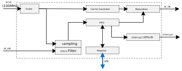
Scaler: Divides the clock based on SCLK to generate the Tx carrier frequency or Rx sampling frequency.
Carrier Generator: Generates Tx carrier symbols and supports flexible duty cycle configuration.
Modulation: Modulates space symbols into carrier symbols.
Glitch Filter: Filters out glitch interference from bus signals at the receiving end.
FIFO
Tx FIFO: Stores Tx carrier symbol count values and data states.
Rx FIFO: Buffers data received from the bus for software to read and process.
Interrupt Control: Generates interrupt events to the processor.
Register: Used to configure IR module parameters.
Working Principle
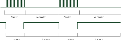
To simplify the IR signal model, an IR signal is divided into several symbols. Symbols are classified into two types: a signal that contains several carrier clock cycles within a specific period is called a Carrier Symbol; a signal that maintains a continuous high or low level within a specific period is called a Space Symbol. The carrier symbol corresponds to the actual signal transmitted in the air, while the space symbol corresponds to the baseband signal before modulation or after demodulation.
Transmit Mode
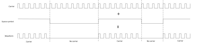
In Tx mode, software first configures modulation parameters to generate a fixed-frequency carrier, then writes space symbols into the Tx FIFO. The Tx module automatically performs modulation and transmits the IR signal. The IR Tx flow is shown in the following figure.
Receive Mode
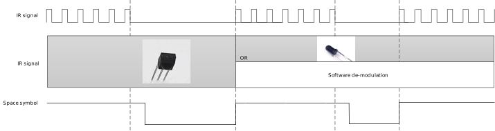
In Rx mode, the IR IP uses the sampling clock as a reference to measure the pulse width of continuous high and low level signals in the input, and writes the measurement results sequentially into the Rx FIFO for software to parse the waveform. The IR IP supports two types of Rx front end:
IR receiver module: The carrier has already been filtered by the front-end module, and the input signal is a clean baseband signal. The IR IP directly captures space symbols, and software only needs to decode them.
IR diode: The input signal still carries the carrier. The IR IP captures carrier symbols, and software needs to demodulate before decoding, which incurs additional CPU overhead.
The IR Rx flow is shown in the following figure.
Functional Description
Scaler
The scaler is the core clock processing unit of the IR module. It takes the system clock (SCLK) as input and generates the required internal clocks for the IR module through programmable division. By configuring the IR_CLK_DIV bit field (12 bits) of the IR_CLK_DIV register, the division factor can be flexibly set: divided clock frequency = SCLK / (IR_CLK_DIV + 1).
Tx Mode
In Tx mode, the scaler output clock is the carrier frequency. The Carrier Generator uses this clock to produce carrier symbols with adjustable duty cycle for driving IR transmission.
For example, when SCLK = 100 MHz and the target carrier frequency is 455 kHz, IR_CLK_DIV = (100M / 455k) - 1.
Rx Mode
In Rx mode, the scaler output clock is the sampling clock. The Rx counter uses the sampling clock as a reference to count the duration of high and low levels in the input signal, and writes the measurement results into the Rx FIFO for software to parse the waveform.
For example, when the Rx sampling clock is 10 MHz and the Rx count value is 0x800000FF, it indicates a high level duration of 255 μs (where bit[31] indicates the input level: 1 = high level, 0 = low level).
The IR IP input clock (SCLK) frequency varies by chip:
The default clock frequency is 40 MHz.
The default clock frequency is 100 MHz.
The default clock frequency is 40 MHz.
The default clock frequency is 40 MHz.
Transmit Mode
FIFO Format
To transmit IR data, data must be written to the IR Tx FIFO register, so understanding its data format is essential. Before transmission, data should be converted to the format defined by the Tx FIFO register. The Tx FIFO register is 32 bits wide, with the following bit definitions:
- Bit[31]:
Data level flag. 1 = high level, 0 = low level.
- Bit[30]:
Data end flag. 1 = last packet of the current transmission, 0 = normal packet.
- Bit[29:28]:
Tx compensation mode. 00 = use Tsample, 11 = use Tcomp_clk.
- Bit[27:0]:
Number of carrier cycles.
Let fcarrierrepresent the carrier frequency (in Hz), and Tdurationrepresent the duration of a carrier symbol or space symbol (in μs). Then:
bit[27:0] = fcarrier× Tduration
FIFO Filling
Taking the NEC protocol as an example, the carrier frequency is 38 kHz. The NEC format is shown in the figure below, consisting of 2 start symbols, 64 data symbols, and 1 stop symbol.
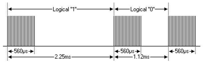
To transmit logic ‘1’, two words must be written to the Tx FIFO register:
First word: bit[31] = 1, bit[30] = 0, bit[27:0] = 38 × 560 / 1000 = 21.
Second word: bit[31] = 0, bit[30] = 0, bit[27:0] = 38 × (2250 - 560) / 1000 = 64.
To transmit logic ‘0’, two words must be written to the Tx FIFO register:
First word: bit[31] = 1, bit[30] = 0, bit[27:0] = 38 × 560 / 1000 = 21.
Second word: bit[31] = 0, bit[30] = 0, bit[27:0] = 38 × (1120 - 560) / 1000 = 21.
Finally, a stop symbol must be sent, with bit[30] = 1 to indicate the end of the current transmission.
Compensation Mechanism
In most application scenarios, the compensation mechanism does not need to be enabled. If precision is not a concern, this section can be skipped.
The Tx waveform consists of several carrier symbols and space symbols. Software calculates the duration of each symbol based on protocol specifications (e.g., NEC), but the duration of space symbols typically cannot be exactly divided by the carrier period. Without compensation, the error accumulates across symbols. To address this, IR Tx introduces a compensation mechanism to reduce the error.
Taking the NEC application as an example, the following figure shows the Tx NEC waveform with fcarrier= 38 kHz, duty = 1/3, and system clock of 100 MHz.
For 38 kHz carrier frequency:
Tcarrier= 1 / fcarrier= 1 / 38 k = 26.31μs
Tcarrier_duty= Tcarrier× duty = 8.77μs
The compensation frequency fcompis an independent clock source that can be set to any desired frequency. In this example, fcomp= 1 MHz, so:
Tcomp= 1 / fcomp= 1μs

Tx NEC waveform
The waveform is divided into four symbols: 560μs carrier symbol, 1690μs space symbol (2250μs - 560μs), 560μs carrier symbol, and 560μs space symbol (1120μs - 560μs). Comparing the two calculation methods below shows that the accuracy is significantly improved when using the compensation mechanism.
Item |
Normal Tx (IR_TX_COMPENSATION = 0) |
Tx Compensation (IR_TX_COMPENSATION = 3) |
|---|---|---|
1st cycle |
560μs ≈ 21 × 26.31 + 8.77 = 561.26μs |
560μs ≈ 21 × 26.31 + 8.77 = 561.26μs |
2nd cycle |
1690μs ≈ 64 × 26.31 + (26.31 - 8.77) = 1701.38μs |
1690μs ≈ (26.31 - 8.77) + 1673 × 1 = 1690.54μs |
3rd cycle |
560μs ≈ 21 × 26.31 + 8.77 = 561.26μs |
560μs ≈ 21 × 26.31 + 8.77 = 561.26μs |
4th cycle |
560μs ≈ 21 × 26.31 + (26.31 - 8.77) = 570.05μs |
560μs ≈ (26.31 - 8.77) + 543 × 1 = 560.54μs |
Tx FIFO Data Value |
0x80000015, 0x00000040; 0x80000015, 0x00000015 |
0x80000015, 0x30000689; 0x80000015, 0x3000021F |
Note
The compensation mechanism only applies to space symbols.
Compensation modes IR_TX_COMPENSATION = 1 and IR_TX_COMPENSATION = 2 are not recommended. If compensation is needed, use IR_TX_COMPENSATION = 3 mode.
If IR_TX_DE_INVERSE is enabled, ensure that the Tx compensation divider IR_TX_COMPE_DIV
IR_TX_COMPE_DIV(register 0xC[11:0]) is no less than the Tx duty count value IR_TX_CONFIGIR_TX_DUTY_NUM(register 0x4[27:16]).
Receive Mode
FIFO Format
When receiving IR data, data must be read from the Rx FIFO register, so understanding its data format is crucial. The Rx FIFO register is 32 bits wide, with bit definitions as follows:
Bit[31] indicates the data level. 1 = high level, 0 = low level.
Bit[30:0] stores the received data, representing the level duration in number of sampling periods.
Let fsamplingdenote the sampling frequency (in kHz), and Tleveldenote the duration of the corresponding high/low level (in μs). Then:
Tlevel= bit[30:0] / fsampling× 1000
Software can further parse the IR protocol and extract the required information based on Tlevel.
Receive Start
Both automatic start and manual start are supported, controlled by IR_RX_START_MODE (register 0x18[27]) of IR_RX_CONFIG.
Automatic Start
Set IR_RX_START_MODE = 1 to enter automatic receive mode. In this mode, when the Rx input signal meets the preset trigger condition, the hardware automatically starts receiving. The trigger type is configured through IR_RX_TRIGGER_MODE:
Value |
Trigger Type |
Description |
|---|---|---|
00 |
IR_RX_FALL_EDGE |
Triggered when a falling edge (high level to low level) is detected |
01 |
IR_RX_RISING_EDGE |
Triggered when a rising edge (low level to high level) is detected |
10 |
IR_RX_DOUBLE_EDGE |
Triggered when any level transition (rising edge or falling edge) is detected |
After enabling the Rx module, the hardware automatically waits for the trigger condition without software intervention.
Manual Start
Set IR_RX_START_MODE = 0 to enter manual receive mode. In this mode, software starts receiving by writing 1 to IR_RX_MAN_START (register 0x18[28]) of IR_RX_CONFIG, suitable for scenarios requiring precise control over the receive start point.
Receive Termination
The Rx module determines receive termination through a counter threshold interrupt. When the duration of a certain level in the input signal exceeds the preset threshold, the IR_RX_CNT_THR_INT_STATUS interrupt is triggered, indicating the end of a complete IR reception.
The termination condition is jointly determined by the following register settings:
Termination level type (
IR_RX_CNT_THR_TRIGGER_LV):0: Trigger interrupt when low level duration >= threshold
1: Trigger interrupt when high level duration >= threshold
Count threshold (
IR_RX_CNT_THR): 31-bit threshold, duration = threshold / sampling frequency.Interrupt enable:
IR_RX_CNT_THR_INT_ENmust be enabled to receive interrupt notification when the condition is met.
Note
The threshold should be configured according to the characteristics of the IR signal in the application scenario. The interval between two IR data frames is typically longer than the duration of any single level within a transmission, so setting this interval as the threshold can reliably distinguish data frames.
Receive Filter
The IR Rx input has a built-in glitch filter that can filter out narrow pulse interference before sampling. The filter width is configured through IR_RX_FILTER_STAGETX (register 0x18[23:21]) of IR_RX_CONFIG. The filter width mappings for each chip are as follows:
Available filter widths: 50 ns, 75 ns, 100 ns, 125 ns, 150 ns, 175 ns, 200 ns, 225 ns.
Available filter widths: 20 ns, 30 ns, 40 ns, 50 ns, 60 ns, 70 ns, 80 ns, 90 ns.
Available filter widths: 50 ns, 75 ns, 100 ns, 125 ns, 150 ns, 175 ns, 200 ns, 225 ns.
Available filter widths: 50 ns, 75 ns, 100 ns, 125 ns, 150 ns, 175 ns, 200 ns, 225 ns.
Interrupt
The interrupt flags supported in each mode are listed below. Each interrupt source can be individually enabled, masked, or cleared.
Mode |
Interrupt Flag |
Description |
|---|---|---|
Tx Mode |
IR_TX_FIFO_OVER_INT |
This interrupt is triggered when data is written to Tx FIFO while it is already full. |
IR_TX_FIFO_LEVEL_INT |
This interrupt is triggered when Tx FIFO usage drops from the threshold to threshold - 1. |
|
IR_TX_FIFO_EMPTY_INT |
This interrupt is triggered when Tx FIFO usage drops from 1 to 0 (i.e., FIFO is empty). |
|
Rx Mode |
IR_RX_FIFO_ERROR_INT |
This interrupt is triggered when data is read from Rx FIFO while it is empty. |
IR_RX_CNT_THR_INT |
This interrupt is triggered when the input level duration exceeds the Rx counter threshold. |
|
IR_RX_CNT_OF_INT |
This interrupt is triggered when the Rx counter overflows without triggering IR_RX_CNT_THR_INT. |
|
IR_RX_FIFO_OF_INT |
This interrupt is triggered when new data is received from the IR input pin while Rx FIFO is already full. |
|
IR_RX_FIFO_LEVEL_INT |
This interrupt is triggered when Rx FIFO usage rises from the threshold to threshold + 1. |
|
IR_RX_FIFO_FULL_INT |
This interrupt is triggered when Rx FIFO becomes full. |
Registers
Base Address: 0x41107000
Name |
Address offset |
Access |
Description |
|---|---|---|---|
000h |
R/W |
||
004h |
R/W |
||
008h |
R |
||
00Ch |
R/W |
||
010h |
R/W |
||
014h |
R/W |
||
018h |
R/W |
||
01Ch |
R |
||
020h |
R/W |
||
024h |
R/W |
||
028h |
R |
||
02Ch |
R |
||
030h |
R |
REG_IR_CLK_DIV
Name: IR clock division register
Size: 32
Address offset: 000h
Read/write access: R/W
Bit |
Symbol |
Access |
INI |
Description |
|---|---|---|---|---|
31:12 |
RSVD |
R |
- |
Reserved |
11:0 |
IR_CLK_DIV |
R/W |
0x0 |
IR_CLK = IO_CLK/(1 + IR_CLK_DIV)
For example: sys_clk = 100MHz, modulation_freq = 455kHz, IR_DIV_NUM = (sys_clk/modulation_freq) - 1
IR_DIV_NUM = (sys_clk/sample clock) - 1 For example: sample clock = 100MHz, IR_DIV_NUM = 0; sample clock = 50MHz, IR_DIV_NUM = 1 |
REG_IR_TX_CONFIG
Name: IR Tx configuration register
Size: 32
Address offset: 004h
Read/write access: R/W
Bit |
Symbol |
Access |
INI |
Description |
|---|---|---|---|---|
31 |
IR_MODE_SEL |
R/W |
0x0 |
|
30 |
IR_TX_START |
R/W |
0x0 |
|
29:28 |
RSVD |
R |
- |
Reserved |
27:16 |
IR_TX_DUTY_NUM |
R/W |
0x0 |
Duty cycle setting for modulation frequency For example: for 1/3 duty cycle, IR_DUTY_NUM = (IR_DIV_NUM+1)/3 Note Set this value equal to IR_DIV_NUM to generate 100% duty waveform. |
15 |
RSVD |
R |
- |
Reserved |
14 |
IR_TX_OUTPUT_INVERSE |
R/W |
0x0 |
|
13 |
IR_TX_DE_INVERSE |
R/W |
0x0 |
|
12:8 |
IR_TX_FIFO_LEVEL_TH |
R/W |
0x0 |
Tx FIFO interrupt threshold. When Tx FIFO depth = < threshold value, interrupt is triggered. |
7 |
RSVD |
R |
- |
Reserved |
6 |
IR_TX_IDLE_STATE |
R/W |
0x0 |
Tx output state in idle
|
5 |
IR_TX_FIFO_OVER_INT_MASK |
R/W |
0x0 |
Tx FIFO overflow interrupt
|
4 |
IR_TX_FIFO_OVER_INT_EN |
R/W |
0x0 |
Tx FIFO overflow interrupt
|
3 |
IR_TX_FIFO_LEVEL_INT_MASK |
R/W |
0x0 |
Tx FIFO level interrupt
|
2 |
IR_TX_FIFO_EMPTY_INT_MASK |
R/W |
0x0 |
Tx FIFO empty interrupt
|
1 |
IR_TX_FIFO_LEVEL_INT_EN |
R/W |
0x0 |
Tx FIFO level interrupt When Tx FIFO offset <= threshold value, interrupt is triggered.
|
0 |
IR_TX_FIFO_EMPTY_INT_EN |
R/W |
0x0 |
Tx FIFO empty interrupt
|
REG_IR_TX_SR
Name: IR Tx FIFO and interrupt status register
Size: 32
Address offset: 008h
Read/write access: R
Bit |
Symbol |
Access |
INI |
Description |
|---|---|---|---|---|
31:16 |
RSVD |
R |
- |
Reserved |
15 |
IR_TX_FIFO_EMPTY |
R |
0x0 |
|
14 |
IR_TX_FIFO_FULL |
R |
0x0 |
|
13:8 |
IR_TX_FIFO_OFFSET |
R |
0x0 |
Tx FIFO offset is from 0 to 32. Note After Tx last packet, hardware can’t clear Tx FIFO offset. |
7:5 |
RSVD |
R |
- |
Reserved |
4 |
IR_TX_STATUS |
R |
0x0 |
|
3 |
RSVD |
R |
- |
Reserved |
2 |
IR_TX_FIFO_OVER_INT_STATUS |
R |
0x0 |
Tx FIFO overflow interrupt
|
1 |
IR_TX_FIFO_LEVEL_INT_STATUS |
R |
0x0 |
When Tx FIFO offset <= threshold value, interrupt is triggered.
|
0 |
IR_TX_FIFO_EMPTY_INT_STATUS |
R |
0x0 |
Tx FIFO empty interrupt
|
REG_IR_TX_COMPE_DIV
Name: IR Tx compensation division register
Size: 32
Address offset: 00Ch
Read/write access: R/W
Bit |
Symbol |
Access |
INI |
Description |
|---|---|---|---|---|
31:12 |
RSVD |
R |
- |
Reserved |
11:0 |
TX_COMPE_DIV |
R/W |
0x0 |
IR_TX_CLK_Period = SCLK/(TX_COMPE_DIV + 1) |
REG_IR_TX_INT_CLR
Name: IR Tx FIFO and interrupt clear register
Size: 32
Address offset: 010h
Read/write access: R/W
Bit |
Symbol |
Access |
INI |
Description |
|---|---|---|---|---|
31:4 |
RSVD |
R |
- |
Reserved |
3 |
IR_TX_FIFO_OVER_INT_CLR |
R/W |
Tx FIFO overflow interrupt Write 1 to clear |
|
2 |
IR_TX_FIFO_LEVEL_INT_CLR |
R/W |
When Tx FIFO offset <= threshold value, interrupt is triggered. Write 1 to clear |
|
1 |
IR_TX_FIFO_EMPTY_INT_CLR |
R/W |
Tx FIFO empty interrupt Write 1 to clear |
|
0 |
IR_TX_FIFO_CLR |
R/W |
Write 1 to clear Tx FIFO |
REG_IR_TX_FIFO
Name: IR Tx FIFO register
Size: 32
Address offset: 014h
Read/write access: R/W
Bit |
Symbol |
Access |
INI |
Description |
|---|---|---|---|---|
31 |
IR_TX_DATA_TYPE |
R/W |
0 |
Data type
|
30 |
IR_TX_DATA_END_FLAG |
R/W |
0 |
|
29:28 |
IR_TX_COMPENSATION |
R/W |
0 |
|
27:0 |
IR_TX_DATA_TIME |
R/W |
0 |
Real active time = (IR_TX_DATA_TIME + 1) * IR_TX_CLK_Period |
REG_IR_RX_CONFIG
Name: IR Rx configuration register
Size: 32
Address offset: 018h
Read/write access: R/W
Bit |
Symbol |
Access |
INI |
Description |
|---|---|---|---|---|
31:29 |
RSVD |
R |
- |
Reserved |
28 |
IR_RX_START |
R/W |
0x0 |
|
27 |
IR_RX_START_MODE |
R/W |
0x0 |
|
26 |
IR_RX_MAN_START |
R/W |
0x0 |
If IR_RX_TRIGGER_MODE =0, writing 1 means starting to check the waveform. |
25:24 |
IR_RX_TRIGGER_MODE |
R/W |
0x0 |
|
23:21 |
IR_RX_FILTER_STAGETX |
R/W |
0x0 |
… |
20 |
RSVD |
R |
- |
Reserved |
19 |
IR_RX_FIFO_ERROR_INT_MASK |
R/W |
0x0 |
Rx FIFO error read interrupt When Rx FIFO is empty, read Rx FIFO and trigger interrupt.
|
18 |
IR_RX_CNT_THR_INT_MASK |
R/W |
0x0 |
Rx count threshold interrupt
|
17 |
IR_RX_FIFO_OF_INT_MASK |
R/W |
0x0 |
Rx FIFO overflow
|
16 |
IR_RX_CNT_OF_INT_MASK |
R/W |
0x0 |
RX counter overflow
|
15 |
IR_RX_FIFO_LEVEL_INT_MASK |
R/W |
0x0 |
Rx FIFO level interrupt
When Rx FIFO offset >= threshold value, this interrupt is triggered. |
14 |
IR_RX_FIFO_FULL_INT_MASK |
R/W |
0x0 |
Rx FIFO full interrupt
|
13 |
IR_RX_FIFO_DISCARD_SET |
R/W |
0x0 |
When FIFO is full, new data is send to FIFO.
|
12:8 |
IR_RX_FIFO_LEVEL_TH |
R/W |
0x0 |
Rx FIFO interrupt threshold When Rx FIFO depth > threshold value, this interrupt is triggered. |
7:6 |
RSVD |
R |
- |
Reserved |
5 |
IR_RX_FIFO_ERROR_INT_EN |
R/W |
0x0 |
Rx FIFO error read interrupt When Rx FIFO is empty, reading the Rx FIFO triggers this interrupt.
|
4 |
IR_RX_CNT_THR_INT_EN |
R/W |
0x0 |
Rx count threshold interrupt
|
3 |
IR_RX_FIFO_OF_INT_EN |
R/W |
0x0 |
RX FIFO overflow
|
2 |
IR_RX_CNT_OF_INT_EN |
R/W |
0x0 |
RX counter overflow
|
1 |
IR_RX_FIFO_LEVEL_INT_EN |
R/W |
0x0 |
Rx FIFO level interrupt When Rx FIFO offset >= threshold value, this interrupt is triggered.
|
0 |
IR_RX_FIFO_FULL_INT_EN |
R/W |
0x0 |
Rx FIFO full interrupt
|
REG_IR_RX_SR
Name: IR Rx FIFO and interrupt status register
Size: 32
Address offset: 01Ch
Read/write access: R
Bit |
Symbol |
Access |
INI |
Description |
|---|---|---|---|---|
31:18 |
RSVD |
R |
- |
Reserved |
17 |
IR_RX_FIFO_EMPTY |
R |
0x0 |
|
16 |
IR_RX_FIFO_FULL |
R |
0x0 |
|
15:14 |
RSVD |
R |
- |
Reserved |
13:8 |
IR_RX_FIFO_OFFSET |
R |
0x0 |
Rx FIFO offset |
7 |
IR_RX_STATE |
R |
0x0 |
|
6 |
RSVD |
R |
- |
Reserved |
5 |
IR_RX_FIFO_ERROR_INT_STATUS |
R |
0x0 |
Rx FIFO error read interrupt status When Rx FIFO is empty, reading the Rx FIFO triggers this interrupt.
|
4 |
IR_RX_CNT_THR_INT_STATUS |
R |
0x0 |
Rx count threshold interrupt status
|
3 |
IR_RX_FIFO_OF_INT_STATUS |
R |
0x0 |
Rx FIFO overflow interrupt status
|
2 |
IR_RX_CNT_OF_INT_STATUS |
R |
0x0 |
Rx counter overflow interrupt status
|
1 |
IR_RX_FIFO_LEVEL_INT_STATUS |
R |
0x0 |
Rx FIFO level interrupt status
|
0 |
IR_RX_FIFO_FULL_INT_STATUS |
R |
0x0 |
Rx FIFO full interrupt status
|
REG_IR_RX_INT_CLR
Name: IR Rx FIFO and interrupt clear register
Size: 32
Address offset: 020h
Read/write access: R/W
Bit |
Symbol |
Access |
INI |
Description |
|---|---|---|---|---|
31:9 |
RSVD |
R |
- |
Reserved |
8 |
IR_RX_FIFO_CLR |
R/W |
Write 1 to clear Rx FIFO |
|
7:6 |
RSVD |
R |
- |
Reserved |
5 |
IR_RX_FIFO_ERROR_INT_CLR |
R/W |
Rx FIFO error read interrupt Write 1 to clear |
|
4 |
IR_RX_CNT_THR_INT_CLR |
R/W |
Rx count threshold interrupt Write 1 to clear |
|
3 |
IR_RX_FIFO_OF_INT_CLR |
R/W |
Rx FIFO overflow interrupt Write 1 to clear |
|
2 |
IR_RX_CNT_OF_INT_CLR |
R/W |
Rx counter overflow interrupt Write 1 to clear |
|
1 |
IR_RX_FIFO_LEVEL_INT_CLR |
R/W |
Rx FIFO level interrupt Write 1 to clear |
|
0 |
IR_RX_FIFO_FULL_INT_CLR |
R/W |
Rx FIFO full interrupt Write 1 to clear |
REG_IR_RX_CNT_INT_SEL
Name: IR Rx count threshold configure register
Size: 32
Address offset: 024h
Read/write access: R/W
Bit |
Symbol |
Access |
INI |
Description |
|---|---|---|---|---|
31 |
IR_RX_CNT_THR_TRIGGER_LV |
R/W |
0x0 |
Trigger level
|
30:0 |
IR_RX_CNT_THR |
R/W |
0x0 |
31-bits threshold |
REG_IR_RX_FIFO
Name: IR Rx FIFO register
Size: 32
Address offset: 028h
Read/write access: R
Bit |
Symbol |
Access |
INI |
Description |
|---|---|---|---|---|
31 |
IR_RX_LEVEL |
R |
0x0 |
Rx Level
|
30:0 |
IR_RX_CNT |
R |
0x0 |
31 bits cycle duration |
REG_IR_VERSION
Name: IR version register
Size: 32
Address offset: 02Ch
Read/write access: R
Bit |
Symbol |
Access |
INI |
Description |
|---|---|---|---|---|
31:0 |
IR_VERSION |
R |
0x1410150A |
IR IP version |
REG_IR_DUMMY
Name: IR Dummy Register
Size: 32
Address offset: 030h
Read/write access: R
Bit |
Symbol |
Access |
INI |
Description |
|---|---|---|---|---|
31:16 |
RSVD |
R |
- |
Reserved |
15:0 |
DUMMY |
R |
0x0 |
Reserved for HW |
Base Address: 0x400EE000
Name |
Address offset |
Access |
Description |
|---|---|---|---|
000h |
R/W |
||
004h |
R/W |
||
008h |
R |
||
00Ch |
R/W |
||
010h |
R/W |
||
014h |
R/W |
||
018h |
R/W |
||
01Ch |
R |
||
020h |
R/W |
||
024h |
R/W |
||
028h |
R |
||
02Ch |
R |
REG_IR_CLK_DIV
Name: IR clock division register
Size: 32
Address offset: 000h
Read/write access: R/W
Bit |
Symbol |
Access |
INI |
Description |
|---|---|---|---|---|
31:12 |
RSVD |
R |
- |
Reserved |
11:0 |
IR_CLK_DIV |
R/W |
0x0 |
IR_CLK = IO_CLK/(1 + IR_CLK_DIV)
For example: sys_clk = 100MHz, modulation_freq = 455kHz, IR_DIV_NUM = (sys_clk/modulation_freq) - 1
IR_DIV_NUM = (sys_clk/sample clock) - 1 For example: sample clock = 100MHz, IR_DIV_NUM = 0; sample clock = 50MHz, IR_DIV_NUM = 1 |
REG_IR_TX_CONFIG
Name: IR Tx configuration register
Size: 32
Address offset: 004h
Read/write access: R/W
Bit |
Symbol |
Access |
INI |
Description |
|---|---|---|---|---|
31 |
IR_MODE_SEL |
R/W |
0x0 |
|
30 |
IR_TX_START |
R/W |
0x0 |
|
29:28 |
RSVD |
R |
- |
Reserved |
27:16 |
IR_TX_DUTY_NUM |
R/W |
0x0 |
Duty cycle setting for modulation frequency For example: for 1/3 duty cycle, IR_DUTY_NUM = (IR_DIV_NUM+1)/3 Note Set this value equals to IR_DIV_NUM to generate 100% duty waveform. |
15 |
RSVD |
R |
- |
Reserved |
14 |
IR_TX_OUTPUT_INVERSE |
R/W |
0x0 |
|
13 |
IR_TX_DE_INVERSE |
R/W |
0x0 |
|
12:8 |
IR_TX_FIFO_LEVEL_TH |
R/W |
0x0 |
Tx FIFO interrupt threshold. When Tx FIFO depth = < threshold value, interrupt is triggered. |
7 |
RSVD |
R |
- |
Reserved |
6 |
IR_TX_IDLE_STATE |
R/W |
0x0 |
Tx output state in idle
|
5 |
IR_TX_FIFO_OVER_INT_MASK |
R/W |
0x0 |
Tx FIFO overflow interrupt
|
4 |
IR_TX_FIFO_OVER_INT_EN |
R/W |
0x0 |
Tx FIFO overflow interrupt
|
3 |
IR_TX_FIFO_LEVEL_INT_MASK |
R/W |
0x0 |
Tx FIFO level interrupt
|
2 |
IR_TX_FIFO_EMPTY_INT_MASK |
R/W |
0x0 |
Tx FIFO empty interrupt
|
1 |
IR_TX_FIFO_LEVEL_INT_EN |
R/W |
0x0 |
Tx FIFO level interrupt When Tx FIFO offset <= threshold value, interrupt is triggered.
|
0 |
IR_TX_FIFO_EMPTY_INT_EN |
R/W |
0x0 |
Tx FIFO empty interrupt
|
REG_IR_TX_SR
Name: IR Tx FIFO and interrupt status register
Size: 32
Address offset: 008h
Read/write access: R
Bit |
Symbol |
Access |
INI |
Description |
|---|---|---|---|---|
31:16 |
RSVD |
R |
- |
Reserved |
15 |
IR_TX_FIFO_EMPTY |
R |
0x0 |
|
14 |
IR_TX_FIFO_FULL |
R |
0x0 |
|
13:8 |
IR_TX_FIFO_OFFSET |
R |
0x0 |
Tx FIFO offset is from 0 to 32. Note After Tx last packet, hardware can’t clear Tx FIFO offset. |
7:5 |
RSVD |
R |
- |
Reserved |
4 |
IR_TX_STATUS |
R |
0x0 |
|
3 |
RSVD |
R |
- |
Reserved |
2 |
IR_TX_FIFO_OVER_INT_STATUS |
R |
0x0 |
Tx FIFO overflow interrupt
|
1 |
IR_TX_FIFO_LEVEL_INT_STATUS |
R |
0x0 |
When Tx FIFO offset <= threshold value, interrupt is triggered.
|
0 |
IR_TX_FIFO_EMPTY_INT_STATUS |
R |
0x0 |
Tx FIFO empty interrupt
|
REG_IR_TX_COMPE_DIV
Name: IR Tx compensation division register
Size: 32
Address offset: 00Ch
Read/write access: R/W
Bit |
Symbol |
Access |
INI |
Description |
|---|---|---|---|---|
31:12 |
RSVD |
R |
- |
Reserved |
11:0 |
TX_COMPE_DIV |
R/W |
0x0 |
IR_TX_CLK_Period = SCLK/(TX_COMPE_DIV + 1) |
REG_IR_TX_INT_CLR
Name: IR Tx FIFO and interrupt clear register
Size: 32
Address offset: 010h
Read/write access: R/W
Bit |
Symbol |
Access |
INI |
Description |
|---|---|---|---|---|
31:4 |
RSVD |
R |
- |
Reserved |
3 |
IR_TX_FIFO_OVER_INT_CLR |
R/W |
Tx FIFO overflow interrupt Write 1 to clear |
|
2 |
IR_TX_FIFO_LEVEL_INT_CLR |
R/W |
When Tx FIFO offset <= threshold value, interrupt is triggered. Write 1 to clear |
|
1 |
IR_TX_FIFO_EMPTY_INT_CLR |
R/W |
Tx FIFO empty interrupt Write 1 to clear |
|
0 |
IR_TX_FIFO_CLR |
R/W |
Write 1 to clear Tx FIFO |
REG_IR_TX_FIFO
Name: IR Tx FIFO register
Size: 32
Address offset: 014h
Read/write access: R/W
Bit |
Symbol |
Access |
INI |
Description |
|---|---|---|---|---|
31 |
IR_TX_DATA_TYPE |
R/W |
0 |
Data type
|
30 |
IR_TX_DATA_END_FLAG |
R/W |
0 |
|
29:28 |
IR_TX_COMPENSATION |
R/W |
0 |
|
27:0 |
IR_TX_DATA_TIME |
R/W |
0 |
Real active time = (IR_TX_DATA_TIME + 1) * IR_TX_CLK_Period |
REG_IR_RX_CONFIG
Name: IR Rx configuration register
Size: 32
Address offset: 018h
Read/write access: R/W
Bit |
Symbol |
Access |
INI |
Description |
|---|---|---|---|---|
31:29 |
RSVD |
R |
- |
Reserved |
28 |
IR_RX_START |
R/W |
0x0 |
|
27 |
IR_RX_START_MODE |
R/W |
0x0 |
|
26 |
IR_RX_MAN_START |
R/W |
0x0 |
If IR_RX_TRIGGER_MODE =0, writing 1 means starting to check the waveform. |
25:24 |
IR_RX_TRIGGER_MODE |
R/W |
0x0 |
|
23:21 |
IR_RX_FILTER_STAGETX |
R/W |
0x0 |
… |
20 |
RSVD |
R |
- |
Reserved |
19 |
IR_RX_FIFO_ERROR_INT_MASK |
R/W |
0x0 |
Rx FIFO error read interrupt When Rx FIFO is empty, read Rx FIFO and trigger interrupt.
|
18 |
IR_RX_CNT_THR_INT_MASK |
R/W |
0x0 |
Rx count threshold interrupt
|
17 |
IR_RX_FIFO_OF_INT_MASK |
R/W |
0x0 |
Rx FIFO overflow
|
16 |
IR_RX_CNT_OF_INT_MASK |
R/W |
0x0 |
RX counter overflow
|
15 |
IR_RX_FIFO_LEVEL_INT_MASK |
R/W |
0x0 |
Rx FIFO level interrupt
When Rx FIFO offset >= threshold value, this interrupt is triggered. |
14 |
IR_RX_FIFO_FULL_INT_MASK |
R/W |
0x0 |
Rx FIFO full interrupt
|
13 |
IR_RX_FIFO_DISCARD_SET |
R/W |
0x0 |
When FIFO is full, new data is send to FIFO.
|
12:8 |
IR_RX_FIFO_LEVEL_TH |
R/W |
0x0 |
Rx FIFO interrupt threshold When Rx FIFO depth > threshold value, this interrupt is triggered. |
7:6 |
RSVD |
R |
- |
Reserved |
5 |
IR_RX_FIFO_ERROR_INT_EN |
R/W |
0x0 |
Rx FIFO error read interrupt When Rx FIFO is empty, reading the Rx FIFO triggers this interrupt.
|
4 |
IR_RX_CNT_THR_INT_EN |
R/W |
0x0 |
Rx count threshold interrupt
|
3 |
IR_RX_FIFO_OF_INT_EN |
R/W |
0x0 |
RX FIFO overflow
|
2 |
IR_RX_CNT_OF_INT_EN |
R/W |
0x0 |
RX counter overflow
|
1 |
IR_RX_FIFO_LEVEL_INT_EN |
R/W |
0x0 |
Rx FIFO level interrupt When Rx FIFO offset >= threshold value, this interrupt is triggered.
|
0 |
IR_RX_FIFO_FULL_INT_EN |
R/W |
0x0 |
Rx FIFO full interrupt
|
REG_IR_RX_SR
Name: IR Rx FIFO and interrupt status register
Size: 32
Address offset: 01Ch
Read/write access: R
Bit |
Symbol |
Access |
INI |
Description |
|---|---|---|---|---|
31:18 |
RSVD |
R |
- |
Reserved |
17 |
IR_RX_FIFO_EMPTY |
R |
0x0 |
|
16 |
IR_RX_FIFO_FULL |
R |
0x0 |
|
15:14 |
RSVD |
R |
- |
Reserved |
13:8 |
IR_RX_FIFO_OFFSET |
R |
0x0 |
Rx FIFO offset |
7 |
IR_RX_STATE |
R |
0x0 |
|
6 |
RSVD |
R |
- |
Reserved |
5 |
IR_RX_FIFO_ERROR_INT_STATUS |
R |
0x0 |
Rx FIFO error read interrupt status When Rx FIFO is empty, reading the Rx FIFO triggers this interrupt.
|
4 |
IR_RX_CNT_THR_INT_STATUS |
R |
0x0 |
Rx count threshold interrupt status
|
3 |
IR_RX_FIFO_OF_INT_STATUS |
R |
0x0 |
Rx FIFO overflow interrupt status
|
2 |
IR_RX_CNT_OF_INT_STATUS |
R |
0x0 |
Rx counter overflow interrupt status
|
1 |
IR_RX_FIFO_LEVEL_INT_STATUS |
R |
0x0 |
Rx FIFO level interrupt status
|
0 |
IR_RX_FIFO_FULL_INT_STATUS |
R |
0x0 |
Rx FIFO full interrupt status
|
REG_IR_RX_INT_CLR
Name: IR Rx FIFO and interrupt clear register
Size: 32
Address offset: 020h
Read/write access: R/W
Bit |
Symbol |
Access |
INI |
Description |
|---|---|---|---|---|
31:9 |
RSVD |
R |
- |
Reserved |
8 |
IR_RX_FIFO_CLR |
R/W |
Write 1 to clear Rx FIFO |
|
7:6 |
RSVD |
R |
- |
Reserved |
5 |
IR_RX_FIFO_ERROR_INT_CLR |
R/W |
Rx FIFO error read interrupt Write 1 to clear |
|
4 |
IR_RX_CNT_THR_INT_CLR |
R/W |
Rx count threshold interrupt Write 1 to clear |
|
3 |
IR_RX_FIFO_OF_INT_CLR |
R/W |
Rx FIFO overflow interrupt Write 1 to clear |
|
2 |
IR_RX_CNT_OF_INT_CLR |
R/W |
Rx counter overflow interrupt Write 1 to clear |
|
1 |
IR_RX_FIFO_LEVEL_INT_CLR |
R/W |
Rx FIFO level interrupt Write 1 to clear |
|
0 |
IR_RX_FIFO_FULL_INT_CLR |
R/W |
Rx FIFO full interrupt Write 1 to clear |
REG_IR_RX_CNT_INT_SEL
Name: IR Rx count threshold configure register
Size: 32
Address offset: 024h
Read/write access: R/W
Bit |
Symbol |
Access |
INI |
Description |
|---|---|---|---|---|
31 |
IR_RX_CNT_THR_TRIGGER_LV |
R/W |
0x0 |
Trigger level
|
30:0 |
IR_RX_CNT_THR |
R/W |
0x0 |
31-bits threshold |
REG_IR_RX_FIFO
Name: IR Rx FIFO register
Size: 32
Address offset: 028h
Read/write access: R
Bit |
Symbol |
Access |
INI |
Description |
|---|---|---|---|---|
31 |
IR_RX_LEVEL |
R |
0x0 |
Rx Level
|
30:0 |
IR_RX_CNT |
R |
0x0 |
31-bits cycle duration |
REG_IR_VERSION
Name: IR IP version register
Size: 32
Address offset: 02Ch
Read/write access: R
Bit |
Symbol |
Access |
INI |
Description |
|---|---|---|---|---|
31:0 |
IR_VERSION |
R |
0x1410150A |
IR IP version |
Base Address: 0x41007000
Name |
Address offset |
Access |
Description |
|---|---|---|---|
000h |
R/W |
||
004h |
R/W |
||
008h |
R |
||
00Ch |
R/W |
||
010h |
R/W |
||
014h |
R/W |
||
018h |
R/W |
||
01Ch |
R |
||
020h |
R/W |
||
024h |
R/W |
||
028h |
R |
||
02Ch |
R |
||
030h |
R |
REG_IR_CLK_DIV
Name: IR clock division register
Size: 32
Address offset: 000h
Read/write access: R/W
Bit |
Symbol |
Access |
INI |
Description |
|---|---|---|---|---|
31:12 |
RSVD |
R |
- |
Reserved |
11:0 |
IR_CLK_DIV |
R/W |
0x0 |
IR_CLK = IO_CLK/(1 + IR_CLK_DIV)
For example: sys_clk = 40MHz, modulation_freq = 455kHz, IR_DIV_NUM = (sys_clk/modulation_freq) - 1
IR_DIV_NUM = (sys_clk/sample clock) - 1 For example: sample clock = 40MHz, IR_DIV_NUM = 0; sample clock = 20MHz, IR_DIV_NUM = 1 |
REG_IR_TX_CONFIG
Name: IR Tx configuration register
Size: 32
Address offset: 004h
Read/write access: R/W
Bit |
Symbol |
Access |
INI |
Description |
|---|---|---|---|---|
31 |
IR_MODE_SEL |
R/W |
0x0 |
|
30 |
IR_TX_START |
R/W |
0x0 |
|
29:28 |
RSVD |
R |
- |
Reserved |
27:16 |
IR_TX_DUTY_NUM |
R/W |
0x0 |
Duty cycle setting for modulation frequency For example: for 1/3 duty cycle, IR_DUTY_NUM = (IR_DIV_NUM+1)/3 Note Set this value equals to IR_DIV_NUM to generate 100% duty waveform. |
15 |
RSVD |
R |
- |
Reserved |
14 |
IR_TX_OUTPUT_INVERSE |
R/W |
0x0 |
|
13 |
IR_TX_DE_INVERSE |
R/W |
0x0 |
|
12:8 |
IR_TX_FIFO_LEVEL_TH |
R/W |
0x0 |
Tx FIFO interrupt threshold. When Tx FIFO depth = < threshold value, interrupt is triggered. |
7 |
RSVD |
R |
- |
Reserved |
6 |
IR_TX_IDLE_STATE |
R/W |
0x0 |
Tx output state in idle
|
5 |
IR_TX_FIFO_OVER_INT_MASK |
R/W |
0x0 |
Tx FIFO overflow interrupt
|
4 |
IR_TX_FIFO_OVER_INT_EN |
R/W |
0x0 |
Tx FIFO overflow interrupt
|
3 |
IR_TX_FIFO_LEVEL_INT_MASK |
R/W |
0x0 |
Tx FIFO level interrupt
|
2 |
IR_TX_FIFO_EMPTY_INT_MASK |
R/W |
0x0 |
Tx FIFO empty interrupt
|
1 |
IR_TX_FIFO_LEVEL_INT_EN |
R/W |
0x0 |
Tx FIFO level interrupt When Tx FIFO offset <= threshold value, interrupt is triggered.
|
0 |
IR_TX_FIFO_EMPTY_INT_EN |
R/W |
0x0 |
Tx FIFO empty interrupt
|
REG_IR_TX_SR
Name: IR Tx FIFO and interrupt status register
Size: 32
Address offset: 008h
Read/write access: R
Bit |
Symbol |
Access |
INI |
Description |
|---|---|---|---|---|
31:16 |
RSVD |
R |
- |
Reserved |
15 |
IR_TX_FIFO_EMPTY |
R |
0x0 |
|
14 |
IR_TX_FIFO_FULL |
R |
0x0 |
|
13:8 |
IR_TX_FIFO_OFFSET |
R |
0x0 |
Tx FIFO offset is from 0 to 32. Note After Tx last packet, hardware can’t clear Tx FIFO offset. |
7:5 |
RSVD |
R |
- |
Reserved |
4 |
IR_TX_STATUS |
R |
0x0 |
|
3 |
RSVD |
R |
- |
Reserved |
2 |
IR_TX_FIFO_OVER_INT_STATUS |
R |
0x0 |
Tx FIFO overflow interrupt
|
1 |
IR_TX_FIFO_LEVEL_INT_STATUS |
R |
0x0 |
When Tx FIFO offset <= threshold value, interrupt is triggered.
|
0 |
IR_TX_FIFO_EMPTY_INT_STATUS |
R |
0x0 |
Tx FIFO empty interrupt
|
REG_IR_TX_COMPE_DIV
Name: IR Tx compensation division register
Size: 32
Address offset: 00Ch
Read/write access: R/W
Bit |
Symbol |
Access |
INI |
Description |
|---|---|---|---|---|
31:12 |
RSVD |
R |
- |
Reserved |
11:0 |
TX_COMPE_DIV |
R/W |
0x0 |
IR_TX_CLK_Period = SCLK/(TX_COMPE_DIV + 1) |
REG_IR_TX_INT_CLR
Name: IR Tx FIFO and interrupt clear register
Size: 32
Address offset: 010h
Read/write access: R/W
Bit |
Symbol |
Access |
INI |
Description |
|---|---|---|---|---|
31:4 |
RSVD |
R |
- |
Reserved |
3 |
IR_TX_FIFO_OVER_INT_CLR |
R/W |
Tx FIFO overflow interrupt Write 1 to clear |
|
2 |
IR_TX_FIFO_LEVEL_INT_CLR |
R/W |
When Tx FIFO offset <= threshold value, interrupt is triggered. Write 1 to clear |
|
1 |
IR_TX_FIFO_EMPTY_INT_CLR |
R/W |
Tx FIFO empty interrupt Write 1 to clear |
|
0 |
IR_TX_FIFO_CLR |
R/W |
Write 1 to clear Tx FIFO |
REG_IR_TX_FIFO
Name: IR Tx FIFO register
Size: 32
Address offset: 014h
Read/write access: R/W
Bit |
Symbol |
Access |
INI |
Description |
|---|---|---|---|---|
31 |
IR_TX_DATA_TYPE |
R/W |
0 |
Data type
|
30 |
IR_TX_DATA_END_FLAG |
R/W |
0 |
|
29:28 |
IR_TX_COMPENSATION |
R/W |
0 |
|
27:0 |
IR_TX_DATA_TIME |
R/W |
0 |
Real active time = (IR_TX_DATA_TIME + 1) * IR_TX_CLK_Period |
REG_IR_RX_CONFIG
Name: IR Rx configuration register
Size: 32
Address offset: 018h
Read/write access: R/W
Bit |
Symbol |
Access |
INI |
Description |
|---|---|---|---|---|
31:29 |
RSVD |
R |
- |
Reserved |
28 |
IR_RX_START |
R/W |
0x0 |
|
27 |
IR_RX_START_MODE |
R/W |
0x0 |
|
26 |
IR_RX_MAN_START |
R/W |
0x0 |
If IR_RX_TRIGGER_MODE =0, writing 1 means starting to check the waveform. |
25:24 |
IR_RX_TRIGGER_MODE |
R/W |
0x0 |
|
23:21 |
IR_RX_FILTER_STAGETX |
R/W |
0x0 |
… |
20 |
RSVD |
R |
- |
Reserved |
19 |
IR_RX_FIFO_ERROR_INT_MASK |
R/W |
0x0 |
Rx FIFO error read interrupt When Rx FIFO is empty, read Rx FIFO and trigger interrupt.
|
18 |
IR_RX_CNT_THR_INT_MASK |
R/W |
0x0 |
Rx count threshold interrupt
|
17 |
IR_RX_FIFO_OF_INT_MASK |
R/W |
0x0 |
Rx FIFO overflow
|
16 |
IR_RX_CNT_OF_INT_MASK |
R/W |
0x0 |
RX counter overflow
|
15 |
IR_RX_FIFO_LEVEL_INT_MASK |
R/W |
0x0 |
Rx FIFO level interrupt
When Rx FIFO offset >= threshold value, this interrupt is triggered. |
14 |
IR_RX_FIFO_FULL_INT_MASK |
R/W |
0x0 |
Rx FIFO full interrupt
|
13 |
IR_RX_FIFO_DISCARD_SET |
R/W |
0x0 |
When FIFO is full, new data is send to FIFO.
|
12:8 |
IR_RX_FIFO_LEVEL_TH |
R/W |
0x0 |
Rx FIFO interrupt threshold When Rx FIFO depth > threshold value, this interrupt is triggered. |
7:6 |
RSVD |
R |
- |
Reserved |
5 |
IR_RX_FIFO_ERROR_INT_EN |
R/W |
0x0 |
Rx FIFO error read interrupt When Rx FIFO is empty, reading the Rx FIFO triggers this interrupt.
|
4 |
IR_RX_CNT_THR_INT_EN |
R/W |
0x0 |
Rx count threshold interrupt
|
3 |
IR_RX_FIFO_OF_INT_EN |
R/W |
0x0 |
RX FIFO overflow
|
2 |
IR_RX_CNT_OF_INT_EN |
R/W |
0x0 |
RX counter overflow
|
1 |
IR_RX_FIFO_LEVEL_INT_EN |
R/W |
0x0 |
Rx FIFO level interrupt When Rx FIFO offset >= threshold value, this interrupt is triggered.
|
0 |
IR_RX_FIFO_FULL_INT_EN |
R/W |
0x0 |
Rx FIFO full interrupt
|
REG_IR_RX_SR
Name: IR Rx FIFO and interrupt status register
Size: 32
Address offset: 01Ch
Read/write access: R
Bit |
Symbol |
Access |
INI |
Description |
|---|---|---|---|---|
31:18 |
RSVD |
R |
- |
Reserved |
17 |
IR_RX_FIFO_EMPTY |
R |
0x0 |
|
16 |
IR_RX_FIFO_FULL |
R |
0x0 |
|
15:14 |
RSVD |
R |
- |
Reserved |
13:8 |
IR_RX_FIFO_OFFSET |
R |
0x0 |
Rx FIFO offset |
7 |
IR_RX_STATE |
R |
0x0 |
|
6 |
RSVD |
R |
- |
Reserved |
5 |
IR_RX_FIFO_ERROR_INT_STATUS |
R |
0x0 |
Rx FIFO error read interrupt status When Rx FIFO is empty, reading the Rx FIFO triggers this interrupt.
|
4 |
IR_RX_CNT_THR_INT_STATUS |
R |
0x0 |
Rx count threshold interrupt status
|
3 |
IR_RX_FIFO_OF_INT_STATUS |
R |
0x0 |
Rx FIFO overflow interrupt status
|
2 |
IR_RX_CNT_OF_INT_STATUS |
R |
0x0 |
Rx counter overflow interrupt status
|
1 |
IR_RX_FIFO_LEVEL_INT_STATUS |
R |
0x0 |
Rx FIFO level interrupt status
|
0 |
IR_RX_FIFO_FULL_INT_STATUS |
R |
0x0 |
Rx FIFO full interrupt status
|
REG_IR_RX_INT_CLR
Name: IR Rx FIFO and interrupt clear register
Size: 32
Address offset: 020h
Read/write access: R/W
Bit |
Symbol |
Access |
INI |
Description |
|---|---|---|---|---|
31:9 |
RSVD |
R |
- |
Reserved |
8 |
IR_RX_FIFO_CLR |
R/W |
Write 1 to clear Rx FIFO |
|
7:6 |
RSVD |
R |
- |
Reserved |
5 |
IR_RX_FIFO_ERROR_INT_CLR |
R/W |
Rx FIFO error read interrupt Write 1 to clear |
|
4 |
IR_RX_CNT_THR_INT_CLR |
R/W |
Rx count threshold interrupt Write 1 to clear |
|
3 |
IR_RX_FIFO_OF_INT_CLR |
R/W |
Rx FIFO overflow interrupt Write 1 to clear |
|
2 |
IR_RX_CNT_OF_INT_CLR |
R/W |
Rx counter overflow interrupt Write 1 to clear |
|
1 |
IR_RX_FIFO_LEVEL_INT_CLR |
R/W |
Rx FIFO level interrupt Write 1 to clear |
|
0 |
IR_RX_FIFO_FULL_INT_CLR |
R/W |
Rx FIFO full interrupt Write 1 to clear |
REG_IR_RX_CNT_INT_SEL
Name: IR Rx count threshold configure register
Size: 32
Address offset: 024h
Read/write access: R/W
Bit |
Symbol |
Access |
INI |
Description |
|---|---|---|---|---|
31 |
IR_RX_CNT_THR_TRIGGER_LV |
R/W |
0x0 |
Trigger level
|
30:0 |
IR_RX_CNT_THR |
R/W |
0x0 |
31-bits threshold |
REG_IR_RX_FIFO
Name: IR Rx FIFO register
Size: 32
Address offset: 028h
Read/write access: R
Bit |
Symbol |
Access |
INI |
Description |
|---|---|---|---|---|
31 |
IR_RX_LEVEL |
R |
0x0 |
Rx Level
|
30:0 |
IR_RX_CNT |
R |
0x0 |
31-bits cycle duration |
REG_IR_VERSION
Name: IR IP version register
Size: 32
Address offset: 02Ch
Read/write access: R
Bit |
Symbol |
Access |
INI |
Description |
|---|---|---|---|---|
31:0 |
IR_VERSION |
R |
0x1410150A |
IR IP version |
REG_IR_DUMMY
Name: Ir Dummy Register
Size: 32
Address offset: 030h
Read/write access: R
Bit |
Symbol |
Access |
INI |
Description |
|---|---|---|---|---|
31:16 |
RSVD |
R |
- |
Reserved |
15:0 |
DUMMY |
R |
0x0 |
Rsvd for hw |
Base Address: 0x4080C000
Name |
Address offset |
Access |
Description |
|---|---|---|---|
000h |
R/W |
||
004h |
R/W |
||
008h |
R |
||
00Ch |
R/W |
||
010h |
R/W |
||
014h |
R/W |
||
018h |
R/W |
||
01Ch |
R |
||
020h |
R/W |
||
024h |
R/W |
||
028h |
R |
||
02Ch |
R |
||
030h |
R |
REG_IR_CLK_DIV
Name: IR clock division register
Size: 32
Address offset: 000h
Read/write access: R/W
Bit |
Symbol |
Access |
INI |
Description |
|---|---|---|---|---|
31:12 |
RSVD |
R |
- |
Reserved |
11:0 |
IR_CLK_DIV |
R/W |
0x0 |
IR_CLK = IO_CLK/(1 + IR_CLK_DIV)
For example: sys_clk = 40MHz, modulation_freq = 455kHz, IR_DIV_NUM = (sys_clk/modulation_freq) - 1
IR_DIV_NUM = (sys_clk/sample clock) - 1 For example: sample clock = 40MHz, IR_DIV_NUM = 0; sample clock = 20MHz, IR_DIV_NUM = 1 |
REG_IR_TX_CONFIG
Name: IR Tx configuration register
Size: 32
Address offset: 004h
Read/write access: R/W
Bit |
Symbol |
Access |
INI |
Description |
|---|---|---|---|---|
31 |
IR_MODE_SEL |
R/W |
0x0 |
|
30 |
IR_TX_START |
R/W |
0x0 |
|
29:28 |
RSVD |
R |
- |
Reserved |
27:16 |
IR_TX_DUTY_NUM |
R/W |
0x0 |
Duty cycle setting for modulation frequency For example: for 1/3 duty cycle, IR_DUTY_NUM = (IR_DIV_NUM+1)/3 Note Set this value equals to IR_DIV_NUM to generate 100% duty waveform. |
15 |
RSVD |
R |
- |
Reserved |
14 |
IR_TX_OUTPUT_INVERSE |
R/W |
0x0 |
|
13 |
IR_TX_DE_INVERSE |
R/W |
0x0 |
|
12:8 |
IR_TX_FIFO_LEVEL_TH |
R/W |
0x0 |
Tx FIFO interrupt threshold. When Tx FIFO depth = < threshold value, interrupt is triggered. |
7 |
RSVD |
R |
- |
Reserved |
6 |
IR_TX_IDLE_STATE |
R/W |
0x0 |
Tx output state in idle
|
5 |
IR_TX_FIFO_OVER_INT_MASK |
R/W |
0x0 |
Tx FIFO overflow interrupt
|
4 |
IR_TX_FIFO_OVER_INT_EN |
R/W |
0x0 |
Tx FIFO overflow interrupt
|
3 |
IR_TX_FIFO_LEVEL_INT_MASK |
R/W |
0x0 |
Tx FIFO level interrupt
|
2 |
IR_TX_FIFO_EMPTY_INT_MASK |
R/W |
0x0 |
Tx FIFO empty interrupt
|
1 |
IR_TX_FIFO_LEVEL_INT_EN |
R/W |
0x0 |
Tx FIFO level interrupt When Tx FIFO offset <= threshold value, interrupt is triggered.
|
0 |
IR_TX_FIFO_EMPTY_INT_EN |
R/W |
0x0 |
Tx FIFO empty interrupt
|
REG_IR_TX_SR
Name: IR Tx FIFO and interrupt status register
Size: 32
Address offset: 008h
Read/write access: R
Bit |
Symbol |
Access |
INI |
Description |
|---|---|---|---|---|
31:16 |
RSVD |
R |
- |
Reserved |
15 |
IR_TX_FIFO_EMPTY |
R |
0x0 |
|
14 |
IR_TX_FIFO_FULL |
R |
0x0 |
|
13:8 |
IR_TX_FIFO_OFFSET |
R |
0x0 |
Tx FIFO offset is from 0 to 32. Note After Tx last packet, hardware can’t clear Tx FIFO offset. |
7:5 |
RSVD |
R |
- |
Reserved |
4 |
IR_TX_STATUS |
R |
0x0 |
|
3 |
RSVD |
R |
- |
Reserved |
2 |
IR_TX_FIFO_OVER_INT_STATUS |
R |
0x0 |
Tx FIFO overflow interrupt
|
1 |
IR_TX_FIFO_LEVEL_INT_STATUS |
R |
0x0 |
When Tx FIFO offset <= threshold value, interrupt is triggered.
|
0 |
IR_TX_FIFO_EMPTY_INT_STATUS |
R |
0x0 |
Tx FIFO empty interrupt
|
REG_IR_TX_COMPE_DIV
Name: IR Tx compensation division register
Size: 32
Address offset: 00Ch
Read/write access: R/W
Bit |
Symbol |
Access |
INI |
Description |
|---|---|---|---|---|
31:12 |
RSVD |
R |
- |
Reserved |
11:0 |
TX_COMPE_DIV |
R/W |
0x0 |
IR_TX_CLK_Period = SCLK/(TX_COMPE_DIV + 1) |
REG_IR_TX_INT_CLR
Name: IR Tx FIFO and interrupt clear register
Size: 32
Address offset: 010h
Read/write access: R/W
Bit |
Symbol |
Access |
INI |
Description |
|---|---|---|---|---|
31:4 |
RSVD |
R |
- |
Reserved |
3 |
IR_TX_FIFO_OVER_INT_CLR |
R/W |
Tx FIFO overflow interrupt Write 1 to clear |
|
2 |
IR_TX_FIFO_LEVEL_INT_CLR |
R/W |
When Tx FIFO offset <= threshold value, interrupt is triggered. Write 1 to clear |
|
1 |
IR_TX_FIFO_EMPTY_INT_CLR |
R/W |
Tx FIFO empty interrupt Write 1 to clear |
|
0 |
IR_TX_FIFO_CLR |
R/W |
Write 1 to clear Tx FIFO |
REG_IR_TX_FIFO
Name: IR Tx FIFO register
Size: 32
Address offset: 014h
Read/write access: R/W
Bit |
Symbol |
Access |
INI |
Description |
|---|---|---|---|---|
31 |
IR_TX_DATA_TYPE |
R/W |
0 |
Data type
|
30 |
IR_TX_DATA_END_FLAG |
R/W |
0 |
|
29:28 |
IR_TX_COMPENSATION |
R/W |
0 |
|
27:0 |
IR_TX_DATA_TIME |
R/W |
0 |
Real active time = (IR_TX_DATA_TIME + 1) * IR_TX_CLK_Period |
REG_IR_RX_CONFIG
Name: IR Rx configuration register
Size: 32
Address offset: 018h
Read/write access: R/W
Bit |
Symbol |
Access |
INI |
Description |
|---|---|---|---|---|
31:29 |
RSVD |
R |
- |
Reserved |
28 |
IR_RX_START |
R/W |
0x0 |
|
27 |
IR_RX_START_MODE |
R/W |
0x0 |
|
26 |
IR_RX_MAN_START |
R/W |
0x0 |
If IR_RX_TRIGGER_MODE =0, writing 1 means starting to check the waveform. |
25:24 |
IR_RX_TRIGGER_MODE |
R/W |
0x0 |
|
23:21 |
IR_RX_FILTER_STAGETX |
R/W |
0x0 |
… |
20 |
RSVD |
R |
- |
Reserved |
19 |
IR_RX_FIFO_ERROR_INT_MASK |
R/W |
0x0 |
Rx FIFO error read interrupt When Rx FIFO is empty, read Rx FIFO and trigger interrupt.
|
18 |
IR_RX_CNT_THR_INT_MASK |
R/W |
0x0 |
Rx count threshold interrupt
|
17 |
IR_RX_FIFO_OF_INT_MASK |
R/W |
0x0 |
Rx FIFO overflow
|
16 |
IR_RX_CNT_OF_INT_MASK |
R/W |
0x0 |
RX counter overflow
|
15 |
IR_RX_FIFO_LEVEL_INT_MASK |
R/W |
0x0 |
Rx FIFO level interrupt
When Rx FIFO offset >= threshold value, this interrupt is triggered. |
14 |
IR_RX_FIFO_FULL_INT_MASK |
R/W |
0x0 |
Rx FIFO full interrupt
|
13 |
IR_RX_FIFO_DISCARD_SET |
R/W |
0x0 |
When FIFO is full, new data is send to FIFO.
|
12:8 |
IR_RX_FIFO_LEVEL_TH |
R/W |
0x0 |
Rx FIFO interrupt threshold When Rx FIFO depth > threshold value, this interrupt is triggered. |
7:6 |
RSVD |
R |
- |
Reserved |
5 |
IR_RX_FIFO_ERROR_INT_EN |
R/W |
0x0 |
Rx FIFO error read interrupt When Rx FIFO is empty, reading the Rx FIFO triggers this interrupt.
|
4 |
IR_RX_CNT_THR_INT_EN |
R/W |
0x0 |
Rx count threshold interrupt
|
3 |
IR_RX_FIFO_OF_INT_EN |
R/W |
0x0 |
RX FIFO overflow
|
2 |
IR_RX_CNT_OF_INT_EN |
R/W |
0x0 |
RX counter overflow
|
1 |
IR_RX_FIFO_LEVEL_INT_EN |
R/W |
0x0 |
Rx FIFO level interrupt When Rx FIFO offset >= threshold value, this interrupt is triggered.
|
0 |
IR_RX_FIFO_FULL_INT_EN |
R/W |
0x0 |
Rx FIFO full interrupt
|
REG_IR_RX_SR
Name: IR Rx FIFO and interrupt status register
Size: 32
Address offset: 01Ch
Read/write access: R
Bit |
Symbol |
Access |
INI |
Description |
|---|---|---|---|---|
31:18 |
RSVD |
R |
- |
Reserved |
17 |
IR_RX_FIFO_EMPTY |
R |
0x0 |
|
16 |
IR_RX_FIFO_FULL |
R |
0x0 |
|
15:14 |
RSVD |
R |
- |
Reserved |
13:8 |
IR_RX_FIFO_OFFSET |
R |
0x0 |
Rx FIFO offset |
7 |
IR_RX_STATE |
R |
0x0 |
|
6 |
RSVD |
R |
- |
Reserved |
5 |
IR_RX_FIFO_ERROR_INT_STATUS |
R |
0x0 |
Rx FIFO error read interrupt status When Rx FIFO is empty, reading the Rx FIFO triggers this interrupt.
|
4 |
IR_RX_CNT_THR_INT_STATUS |
R |
0x0 |
Rx count threshold interrupt status
|
3 |
IR_RX_FIFO_OF_INT_STATUS |
R |
0x0 |
Rx FIFO overflow interrupt status
|
2 |
IR_RX_CNT_OF_INT_STATUS |
R |
0x0 |
Rx counter overflow interrupt status
|
1 |
IR_RX_FIFO_LEVEL_INT_STATUS |
R |
0x0 |
Rx FIFO level interrupt status
|
0 |
IR_RX_FIFO_FULL_INT_STATUS |
R |
0x0 |
Rx FIFO full interrupt status
|
REG_IR_RX_INT_CLR
Name: IR Rx FIFO and interrupt clear register
Size: 32
Address offset: 020h
Read/write access: R/W
Bit |
Symbol |
Access |
INI |
Description |
|---|---|---|---|---|
31:9 |
RSVD |
R |
- |
Reserved |
8 |
IR_RX_FIFO_CLR |
R/W |
Write 1 to clear Rx FIFO |
|
7:6 |
RSVD |
R |
- |
Reserved |
5 |
IR_RX_FIFO_ERROR_INT_CLR |
R/W |
Rx FIFO error read interrupt Write 1 to clear |
|
4 |
IR_RX_CNT_THR_INT_CLR |
R/W |
Rx count threshold interrupt Write 1 to clear |
|
3 |
IR_RX_FIFO_OF_INT_CLR |
R/W |
Rx FIFO overflow interrupt Write 1 to clear |
|
2 |
IR_RX_CNT_OF_INT_CLR |
R/W |
Rx counter overflow interrupt Write 1 to clear |
|
1 |
IR_RX_FIFO_LEVEL_INT_CLR |
R/W |
Rx FIFO level interrupt Write 1 to clear |
|
0 |
IR_RX_FIFO_FULL_INT_CLR |
R/W |
Rx FIFO full interrupt Write 1 to clear |
REG_IR_RX_CNT_INT_SEL
Name: IR Rx count threshold configure register
Size: 32
Address offset: 024h
Read/write access: R/W
Bit |
Symbol |
Access |
INI |
Description |
|---|---|---|---|---|
31 |
IR_RX_CNT_THR_TRIGGER_LV |
R/W |
0x0 |
Trigger level
|
30:0 |
IR_RX_CNT_THR |
R/W |
0x0 |
31-bits threshold |
REG_IR_RX_FIFO
Name: IR Rx FIFO register
Size: 32
Address offset: 028h
Read/write access: R
Bit |
Symbol |
Access |
INI |
Description |
|---|---|---|---|---|
31 |
IR_RX_LEVEL |
R |
0x0 |
Rx Level
|
30:0 |
IR_RX_CNT |
R |
0x0 |
31-bits cycle duration |
REG_IR_VERSION
Name: IR IP version register
Size: 32
Address offset: 02Ch
Read/write access: R
Bit |
Symbol |
Access |
INI |
Description |
|---|---|---|---|---|
31:0 |
IR_VERSION |
R |
0x1410150A |
IR IP version |
REG_IR_DUMMY
Name: Ir Dummy Register
Size: 32
Address offset: 030h
Read/write access: R
Bit |
Symbol |
Access |
INI |
Description |
|---|---|---|---|---|
31:16 |
RSVD |
R |
- |
Reserved |
15:0 |
DUMMY |
R |
0x0 |
Rsvd for hw |