RTL8710E-Realtek IoT | Wi-Fi SoC

Realtek Ameba IoT Chip Selection
Ameba IoT wireless solutions, featuring high integration, stable performance, low power consumption, and enhanced security
Highlights
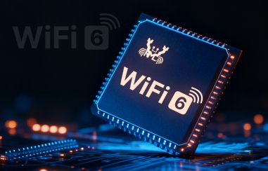
RTL8710E is designed based on Arm Cortex-M and RISC-V dual-core architecture, providing 802.11ax Wi-Fi 6 standard 2.4GHz wireless connectivity capability (20MHz bandwidth, 114.7Mbps PHY rate) and Bluetooth LE 5.x support. The chip implements key Wi-Fi 6 technical features such as OFDMA, Target Wake Time, LDPC and STBC, while Bluetooth functions include 2Mbps high-speed mode, long-range transmission, advertising extension, periodic advertising and direction finding, along with Scatternet multi-role concurrency and SIG Mesh network support. The security architecture contains AES/SHA hardware encryption engine, ECDSA/ECDH public key encryption, Secure Boot, Flash real-time decryption, OTP secure storage, true random number generator, HUK key derivation and authenticated debug access control, supports Wi-Fi Card mode, P2P/NAN direct connection and MCC multi-channel concurrency advanced wireless functions, suitable for smart bulbs, smart plugs, sensor nodes and various smart home appliances requiring Wi-Fi 6 connectivity.

Integrating various security features including asymmetric encryption, TRNG, HUK, OTP storage, Flash XIP decryption, etc., it provides security protection for customer's products.

Incorporating advanced technologies such as OFDMA, MU-MIMO, TWT and Extended Range, it effectively alleviates wireless resource congestion, enhances weak signal coverage, significantly improves transmission quality, reduces latency, and extends the battery life of IoT devices
System Architecture

- RISC-V RV32IMAFC Architecture
- 400MHz Single-Issue In-Order Pipeline
- 16KB I-Cache
- 16KB D-Cache
- Open-source ISA architecture, supports custom extensions
- Armv8.1-M Architecture
- Arm Cortex®-M55 ISA compatible
- Up to 400MHz, 3-stage pipeline
- 16KB I-Cache
- 16KB D-Cache
- FPU/DSP instruction extensions

- 512KB/768KB SRAM
- QSPI NOR Flash: Up to 100MHz
- DQ8 DDR PSRAM: Up to 250MHz

Part Number
| Package number | RTL8710ECF-VA2-CG | RTL8710ECF-VA3-CG | RTL8710ECF-VT3-CG | RTL8710ECM-VA2-CG |
|---|---|---|---|---|
| Real-M300 | 400MHz | 400MHz | 400MHz | 400MHz |
| KR4 | 400MHz | 400MHz | 400MHz | 400MHz |
| On-chip SRAM | 512KB | 512KB | 768KB | 512KB |
| Arm TrustZone | ||||
| NOR Flash | 4MB | 8MB | 8MB | |
| PSRAM | 4MB | |||
| Wi-Fi | Wi-Fi 6 (2.4GHz) | Wi-Fi 6 (2.4GHz) | Wi-Fi 6 (2.4GHz) | Wi-Fi 6 (2.4GHz) |
| Bluetooth | LE | LE | LE | LE |
| Operating voltage | 2.97V ~ 3.63V | 2.97V ~ 3.63V | 2.97V ~ 3.63V | 2.97V ~ 3.63V |
| Operating temperature | -20°C ~ 85°C | -20°C ~ 85°C | -40°C ~ 105°C | -20°C ~ 85°C |
| Package (mm) | QFN48 (6 x 6) | QFN48 (6 x 6) | QFN48 (6 x 6) | QFN48 (6 x 6) |
Peripheral Interfaces
| FUNCTION | RTL8710ECF | RTL8710ECM |
|---|---|---|
| GPIO | 25 | 18 |
| SPI | 2 | 2 |
| UART | 5 | 5 |
| I2C | 2 | 2 |
| I2S | 2 | 2 |
| PDM | 1 | 1 |
| Digital microphone | 4 | 4 |
| ADC and Cap-touch | 10 | 10 |
| SWD Interface | 1 | 1 |
| General Timer | 13 | 13 |
| Capture Timer | 1 | 1 |
| RTC | 1 | 1 |
| NeoPixel LED | 1 | 1 |
| PWM | 8 | 8 |
| IWDG | 1 | 1 |
| System WDG | 2 | 2 |
| GDMA | 8 | 8 |
| Thermal | 1 | 1 |
Security Features
We consistently prioritize security as the core of our products, offering our customers a rich array of security features through hardware design and providing exceptional hardware-based attack resistance, helping to create IoT products with ultimate security.

| Features | Filter | RTL8721Dx | RTL8720E | RTL8710E | RTL8726E | RTL8713E | RTL8730E | RTL8721F | RTL8720F | RTL872xD | RTL8735B |
|---|---|---|---|---|---|---|---|---|---|---|---|
| AES Hardware Engine | |||||||||||
| SHA Hardware Engine | |||||||||||
| ECDSA/ECDH Hardware Engine | |||||||||||
| EDDSA Hardware Engine | |||||||||||
| RSA Hardware Engine | |||||||||||
| Secure Boot | |||||||||||
| Flash OTF Decryption | |||||||||||
| Arm TrustZone | |||||||||||
| OTP Secure Storage | |||||||||||
| True Random Number Generator | |||||||||||
| HUK Derivation Mechanism | |||||||||||
| Authenticated Debug Access |
In addition to the essential symmetric encryption engines like AES for IoT, we also provide computationally more intensive asymmetric encryption algorithms ECDSA. This greatly alleviates the computational burden on the CPU and improves encryption and decryption speeds
Based on asymmetric encryption and digital signature mechanisms, it verifies public key hashes and firmware signatures. This process can prevent tampering and rollback attacks, ensuring that the device only runs trusted firmware
Supports both embedded and external Flash, with independent key encryption for multiple firmware. When the CPU executes encrypted firmware, it is decrypted in real-time by hardware, with nearly imperceptible performance impact. Supports unique encryption for each device, preventing injection and cloning attacks
Physical-level anti-extraction, key area locked for access only by the security engine, tamper-resistant and read-proof. Supports independent secure zones and CRC verification
Generates high-security random numbers based on physical entropy sources. Certified by NIST for randomness. Provides unpredictability to the system, resistant to prediction attacks
Hardware Unique Key (HUK) with physical isolation protection, unreadable and unclonable, used for secure derivation of application keys
Strict control over debug interface access through authentication mechanisms. Supports authorized access and permanent closure, eliminating physical debug attacks. Meets security management requirements at different stages of the product lifecycle, effectively enhancing overall security
Security Certifications Support
We offer support for multiple security certifications. By providing these advanced security features and certification support, we aim to assist our customers in efficiently meeting various market entry requirements, ensuring the security and competitiveness of their products. Most of our chips are capable of achieving PSA Certified Level 2 and Level 3, with some chips already having completed PSA Certified Level 2 certification.
Wireless Connectivity
Wi-Fi Feature List
| Features | Filter | RTL8721Dx | RTL8720E | RTL8710E | RTL8726E | RTL8713E | RTL8730E | RTL8721F | RTL8720F | RTL872xD | RTL8735B |
|---|---|---|---|---|---|---|---|---|---|---|---|
| Frequency | 2.4GHz/5GHz | 2.4GHz | 2.4GHz | 2.4GHz | 2.4GHz | 2.4GHz/5GHz | 2.4GHz/5GHz | 2.4GHz | 2.4GHz/5GHz | 2.4GHz/5GHz | |
| Bandwidth | 40MHz | 20MHz | 20MHz | 20MHz | 20MHz | 20MHz | 20MHz | 20MHz | 40MHz | 20MHz | |
| Maximum PHY rate | 150Mbps | 114.7Mbps | 114.7Mbps | 114.7Mbps | 114.7Mbps | 114.7Mbps | 114.7Mbps | 114.7Mbps | 150Mbps | 72Mbps | |
| 802.11a | |||||||||||
| 802.11ax (Wi-Fi6) | |||||||||||
| 802.11b/g/n | |||||||||||
| 802.11e/i/w/d/k/v/r | |||||||||||
| WMM/WPA1~3/WPS/ 802.1X/EAP |
|||||||||||
| UL LDPC | |||||||||||
| DL STBC | |||||||||||
| Auto Antenna Diversity | |||||||||||
| CSI | |||||||||||
| MCC | |||||||||||
| R-MESH | |||||||||||
| Wi-Fi Card Mode | |||||||||||
| P2P/NAN | |||||||||||
| TWT |
Bluetooth Feature List
| Features | Filter | RTL8721Dx | RTL8720E | RTL8710E | RTL8726E | RTL8713E | RTL8730E | RTL8721F | RTL8720F | RTL872xD | RTL8735B |
|---|---|---|---|---|---|---|---|---|---|---|---|
| Bluetooth Mode | Bluetooth LE | Bluetooth LE | Bluetooth LE | Bluetooth Dual Mode | Bluetooth Dual Mode | Bluetooth Dual Mode | Bluetooth LE | Bluetooth LE | Bluetooth LE | Bluetooth LE | |
| Bluetooth BR/EDR | |||||||||||
| LE Audio | |||||||||||
|
Dedicated antenna for Bluetooth |
|||||||||||
| Scatternet | |||||||||||
| LE 2Mpbs PHY | |||||||||||
| LE Long Range | |||||||||||
|
LE Advertising Extensions |
|||||||||||
| Periodic Advertising | |||||||||||
| Periodic Advertising Sync Transfer |
|||||||||||
|
Direction Finding (AoA/AoD) |
|||||||||||
|
LE Isochronous Channels (CIS/BIS) |
|||||||||||
| LE Power Control | |||||||||||
| SIG Mesh | |||||||||||
| High-Power Mode | TBD |
System Power Consumption
| Mode | Wi-Fi | Power Consumption | Unit | Comment |
|---|---|---|---|---|
| Deep-Sleep | OFF | 57.4 | µA | PSRAM package |
| Sleep | OFF | 700 | µA | PSRAM package |
| Active | OFF | 20.0 | mA | 1.25V WFI mode, CPU=400MHz |
| WoWLAN | DTIM=3 | 1.48 | mA | 2.4G mode |
| WoWLAN | DTIM=10 | 1.36 | mA | 2.4G mode |
Note:
- Test conditions: 3.3V, 25°C
- WoWLAN: System average power consumption
Application Scenarios

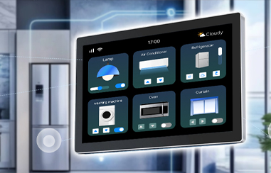
Ameba IC leverages Wi-Fi and BLE dual-mode capabilities to build a smart home network hub, enabling cross-protocol interconnection between Bluetooth and Wi-Fi devices. It supports multi-node BLE Mesh and Matter protocol for large-scale device networking. Based on Arm® security architecture and PSA certification, it ensures encrypted transmission of device control commands and private data. The ultra-low power design meets 24-hour standby requirements, while rich peripherals can directly drive sensors, lighting modules, and actuators. Voice control, scenario linkage, and remote management create an efficient and convenient whole-house smart ecosystem.

Ameba IC provides reliable industrial control solutions with single-band 2.4GHz Wi-Fi 6 and Bluetooth dual-mode connectivity optimized for stable industrial environments. The heterogeneous dual-core architecture delivers high computational performance while maintaining low power consumption. Built-in multi-channel high-precision ADCs enable accurate acquisition of temperature, humidity, pressure, and other sensor data. Rich peripheral interfaces including multiple UART, SPI, and I2C support seamless integration with industrial sensors, actuators, and PLCs. Integrated security features ensure device and data security in critical industrial applications. The industrial-grade wide-temperature design operates reliably in harsh environments, making it ideal for industrial IoT gateways, machine monitoring terminals, and smart factory sensors.
Ameba IC is equipped with built-in multi-channel high-precision ADCs, which can accurately collect core data such as voltage, current and battery cell temperature. Combined with Wi-Fi 6 and Bluetooth dual-mode communication, it enables real-time monitoring and remote regulation of energy storage device status. Integrated with an Arm® security architecture and hardware encryption engine, the IC ensures encrypted storage and transmission of energy storage data and supports full-life-cycle traceability of batteries. Its industrial-grade wide-temperature design adapts to complex outdoor energy storage conditions, while ultra-low power consumption enables long-lasting standby, and rich peripherals can directly drive display and alarm modules, making it an ideal core for building the next generation of intelligent, secure and efficient energy storage devices.
Ameba IC integrates three core capabilities: local scenario control, multi-modal human-machine interaction, and wired-wireless convergence, enabling intelligent upgrades for wall-mounted switches. It supports multi-channel PWM dimming interfaces, a touch-sensing engine, a programmable LED controller, and industrial-grade expansion interfaces, allowing precise driving of various execution units and enabling human-machine interaction. The chip integrates Wi-Fi and Bluetooth for multi-mode networking, and its hardware infrared engine supports mainstream protocols. With chip-level power management, it maintains wireless connectivity in standby mode with ultra-low power consumption, meeting the demands of high-reliability, low-latency wall-mounted control scenarios.

Ameba IC leverages BLE and dual-band Wi-Fi dual-mode capabilities to enable protocol conversion and relay transmission between Bluetooth terminal data and the cloud. With BLE long-range communication features, combined with high transmit power and excellent receive sensitivity, it supports multi-node BLE Mesh networking and is compatible with multi-master/slave scatternet architecture. This effectively expands the gateway coverage, facilitates Bluetooth device access in scenarios such as smart homes and buildings, and achieves efficient interconnection of large-scale nodes. Meanwhile, the PSA Level 2 security mechanism ensures data transmission privacy.
Ameba IC leverages a multi-core heterogeneous architecture and rich peripherals to efficiently execute inversion control algorithms and precisely drive multiple PWM channels, ensuring high-efficiency power conversion and reducing energy loss. Equipped with built-in multi-channel high-precision ADCs, it accurately collects photovoltaic voltage, current and inversion status data, enabling real-time monitoring of power generation status via Wi-Fi and Bluetooth dual-mode communication. Integrated with an Arm® security architecture and hardware encryption engine, it safeguards system security at the underlying level. With its industrial-grade wide-temperature design, it helps build an efficient, secure and long-lasting solution for micro inverters.
Development Resources
Software Resources
| Icon | Resource Name | Link |
|---|---|---|
 |
FreeRTOS SDK Download | Link |
 |
FreeRTOS SDK Guide | Link |
 |
Development Tools | Link |
|
VS Code Extension | Link |
Hardware Resources
| Icon | Resource Name | Link |
|---|---|---|
|
Datasheet | Link |
|
Pin Multiplexing | Link |
|
Pin Assignment Tool | Link |
 |
Hardware Design Guide | Link |
EVB Purchase
 |
Modules & EVBs | Link |