Introduction
The thermal sensor of the chip is used to monitor the temperature inside the chip, and provide low-temperature warning, high-temperature warning and over-temperature protection.
When the temperature exceeds the limit high-temperature threshold, an interrupt will be sent to the CPU, and the CPU can reduce the frequency.
When the temperature exceeds the limit low-temperature threshold, an interrupt will be sent to the CPU, and the CPU can increase the frequency.
When the temperature exceeds the limit over-temperature protection threshold, the hardware will automatically power down for over-temperature protection.
Features
No calibration
Measurement range: -40°C ~ 125°C
Variation: ±1.5°C (typical), ±5°C (worst case)
Resolution: 0.0125°C
Clock: 2MHz
19-bit thermal temperature value: 1 signed bit, 8 integer bits, and 10 decimal bits
Provides low-temperature warning, high-temperature warning and over-temperature protection
Provides access protection for thermal enable bit and over-temperature enable bit
No calibration
Measurement range: -40°C ~ 125°C
Variation: ±1.5°C (typical), ±5°C (worst case)
Resolution: 0.0125°C
Clock: 2MHz
19-bit thermal temperature value: 1 signed bit, 8 integer bits, and 10 decimal bits
Provides low-temperature warning, high-temperature warning and over-temperature protection
Provides access protection for thermal enable bit and over-temperature enable bit
No calibration
Measurement range: -40°C ~ 125°C
Variation: ±1.5°C (typical), ±5°C (worst case)
Resolution: 0.0125°C
Clock: 2MHz
19-bit thermal temperature value: 1 signed bit, 8 integer bits, and 10 decimal bits
Provides low-temperature warning, high-temperature warning and over-temperature protection
Provides access protection for thermal enable bit and over-temperature enable bit
No calibration
Measurement range: -40°C ~ 125°C
Variation: ±1.5°C (typical), ±5°C (worst case)
Resolution: 0.0125°C
Clock: 2MHz
19-bit thermal temperature value: 1 signed bit, 8 integer bits, and 10 decimal bits
Provides low-temperature warning, high-temperature warning and over-temperature protection
Provides access protection for thermal enable bit and over-temperature enable bit
No calibration
Measurement range: -40°C ~ 125°C
Variation: ±1.5°C (typical), ±5°C (worst case)
Resolution: 0.0125°C
Clock: 2MHz
19-bit thermal temperature value: 1 signed bit, 8 integer bits, and 10 decimal bits
Provides low-temperature warning, high-temperature warning and over-temperature protection
Provides access protection for thermal enable bit and over-temperature enable bit
No calibration
Measurement range: -40°C ~ 125°C
Variation: ±1.5°C (typical), ±5°C (worst case)
Resolution: 0.0125°C
Clock: 2MHz
19-bit thermal temperature value: 1 signed bit, 8 integer bits, and 10 decimal bits
Provides low-temperature warning, high-temperature warning and over-temperature protection
Provides access protection for thermal enable bit and over-temperature enable bit
Measurement range: ─40°C ~ 125°C
Variation: ±5°C (typical), ±10°C (worst)
Provides low- temperature warning, high-temperature warning and over-temperature protection
Provides thermal enable and over-temperature protection enable write access control
Block Diagram
The thermal block diagram is shown in the following figure.

The thermal module includes the following sub-modules:
Bias circuit
Generates bias current for bipolar core.
Bipolar core
Generates temperature-dependent voltages ΔV_BE and V_BE.
∑-∆ ADC
Contains a ∑-∆ modulator and a decimation filter.
Outputs a temperature-dependent digital value.
Controller
Controls and manages the interrupts.
Controls low-temperature warning, high-temperature warning, and over-temperature protection.
Register
Contains configuration registers, result registers, and interrupt registers.
Provides the interface to software.
Allows the measured temperature to be read directly from the registers.
Bipolar Core
To produce a digital temperature reading, a ratio-metric measurement has to be performed: a temperature-dependent signal has to be compared to a reference signal.
While virtually every device has temperature-dependent characteristics, two diode-connected substrate PNP transistors are used to generate two voltages: one with a negative temperature coefficient (V_BE) and one with a positive temperature coefficient (ΔV_BE). They can be used to generate both a voltage that is accurately proportional to absolute temperature (PTAT), and a temperature-independent bandgap reference voltage.
The block diagram of the substrate PNP transistors is shown in the following figure.

The relationship between temperature, V_BE, and ΔV_BE is shown in the following figure.

μ = (α * ΔV_BE) / (V_BE + α * ΔV_BE) = V_PTAT / V_REF
V_PTAT = α * ΔV_BE, which is proportional to absolute temperature.
V_REF = V_BE + α * ΔV_BE, which is a conventional bandgap reference voltage (around 1.2V), with a zero temperature coefficient.
μ is proportional to temperature; α should be chosen reasonably to achieve the target V_REF.
∑-∆ ADC
The ∑-∆ ADC contains a ∑-∆ modulator and a decimation filter. V_BE and ΔV_BE are input to a ∑-∆ modulator, which produces a bitstream bs, of which the average value μ is equal to the ratio of α * ΔV_BE and V_REF. A decimation filter is used to filter the quantization noise from the bitstream bs and perform the required scaling to obtain the ADC output Dout.
The block diagram of the ∑-∆ modulator is shown in the following figure.
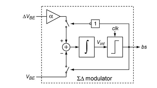
The ∑-∆ modulator consists of a loop filter and a clocked comparator. For simplicity, only a first-order loop filter is shown. In the actual modulator, a second-order filter is used. Every clock cycle, the comparator produces a bit of the bitstream bs based on the polarity of the output Vint of the loop filter. The feedback is arranged to drive the output of the integrator to zero.
If the bitstream in a given clock cycle is zero, α * ΔV_BE is integrated, while -V_BE is integrated if the bitstream is one. This can be expressed as follows:

As a result of the feedback in the modulator, the average input to the integrator is zero. In other words, the charge added by α * ΔV_BE is balanced by the charge removed by -V_BE.

So ∑-∆ modulator realizes the quantization of μ.
The thermal block diagram is shown in the following figure.
The thermal module includes the following sub-modules:
Bias circuit
Generates bias current for bipolar core.
Bipolar core
Generates temperature-dependent voltages ΔV_BE and V_BE.
∑-∆ ADC
Contains a ∑-∆ modulator and a decimation filter.
Outputs a temperature-dependent digital value.
Controller
Controls and manages the interrupts.
Controls low-temperature warning, high-temperature warning, and over-temperature protection.
Register
Contains configuration registers, result registers, and interrupt registers.
Provides the interface to software.
Allows the measured temperature to be read directly from the registers.
Bipolar Core
To produce a digital temperature reading, a ratio-metric measurement has to be performed: a temperature-dependent signal has to be compared to a reference signal.
While virtually every device has temperature-dependent characteristics, two diode-connected substrate PNP transistors are used to generate two voltages: one with a negative temperature coefficient (V_BE) and one with a positive temperature coefficient (ΔV_BE). They can be used to generate both a voltage that is accurately proportional to absolute temperature (PTAT), and a temperature-independent bandgap reference voltage.
The block diagram of the substrate PNP transistors is shown in the following figure.
The relationship between temperature, V_BE, and ΔV_BE is shown in the following figure.
μ = (α * ΔV_BE) / (V_BE + α * ΔV_BE) = V_PTAT / V_REF
V_PTAT = α * ΔV_BE, which is proportional to absolute temperature.
V_REF = V_BE + α * ΔV_BE, which is a conventional bandgap reference voltage (around 1.2V), with a zero temperature coefficient.
μ is proportional to temperature; α should be chosen reasonably to achieve the target V_REF.
∑-∆ ADC
The ∑-∆ ADC contains a ∑-∆ modulator and a decimation filter. V_BE and ΔV_BE are input to a ∑-∆ modulator, which produces a bitstream bs, of which the average value μ is equal to the ratio of α * ΔV_BE and V_REF. A decimation filter is used to filter the quantization noise from the bitstream bs and perform the required scaling to obtain the ADC output Dout.
The block diagram of the ∑-∆ modulator is shown in the following figure.
The ∑-∆ modulator consists of a loop filter and a clocked comparator. For simplicity, only a first-order loop filter is shown. In the actual modulator, a second-order filter is used. Every clock cycle, the comparator produces a bit of the bitstream bs based on the polarity of the output Vint of the loop filter. The feedback is arranged to drive the output of the integrator to zero.
If the bitstream in a given clock cycle is zero, α * ΔV_BE is integrated, while -V_BE is integrated if the bitstream is one. This can be expressed as follows:
As a result of the feedback in the modulator, the average input to the integrator is zero. In other words, the charge added by α * ΔV_BE is balanced by the charge removed by -V_BE.
So ∑-∆ modulator realizes the quantization of μ.
The thermal block diagram is shown in the following figure.
The thermal module includes the following sub-modules:
Bias circuit
Generates bias current for bipolar core.
Bipolar core
Generates temperature-dependent voltages ΔV_BE and V_BE.
∑-∆ ADC
Contains a ∑-∆ modulator and a decimation filter.
Outputs a temperature-dependent digital value.
Controller
Controls and manages the interrupts.
Controls low-temperature warning, high-temperature warning, and over-temperature protection.
Register
Contains configuration registers, result registers, and interrupt registers.
Provides the interface to software.
Allows the measured temperature to be read directly from the registers.
Bipolar Core
To produce a digital temperature reading, a ratio-metric measurement has to be performed: a temperature-dependent signal has to be compared to a reference signal.
While virtually every device has temperature-dependent characteristics, two diode-connected substrate PNP transistors are used to generate two voltages: one with a negative temperature coefficient (V_BE) and one with a positive temperature coefficient (ΔV_BE). They can be used to generate both a voltage that is accurately proportional to absolute temperature (PTAT), and a temperature-independent bandgap reference voltage.
The block diagram of the substrate PNP transistors is shown in the following figure.
The relationship between temperature, V_BE, and ΔV_BE is shown in the following figure.
μ = (α * ΔV_BE) / (V_BE + α * ΔV_BE) = V_PTAT / V_REF
V_PTAT = α * ΔV_BE, which is proportional to absolute temperature.
V_REF = V_BE + α * ΔV_BE, which is a conventional bandgap reference voltage (around 1.2V), with a zero temperature coefficient.
μ is proportional to temperature; α should be chosen reasonably to achieve the target V_REF.
∑-∆ ADC
The ∑-∆ ADC contains a ∑-∆ modulator and a decimation filter. V_BE and ΔV_BE are input to a ∑-∆ modulator, which produces a bitstream bs, of which the average value μ is equal to the ratio of α * ΔV_BE and V_REF. A decimation filter is used to filter the quantization noise from the bitstream bs and perform the required scaling to obtain the ADC output Dout.
The block diagram of the ∑-∆ modulator is shown in the following figure.
The ∑-∆ modulator consists of a loop filter and a clocked comparator. For simplicity, only a first-order loop filter is shown. In the actual modulator, a second-order filter is used. Every clock cycle, the comparator produces a bit of the bitstream bs based on the polarity of the output Vint of the loop filter. The feedback is arranged to drive the output of the integrator to zero.
If the bitstream in a given clock cycle is zero, α * ΔV_BE is integrated, while -V_BE is integrated if the bitstream is one. This can be expressed as follows:
As a result of the feedback in the modulator, the average input to the integrator is zero. In other words, the charge added by α * ΔV_BE is balanced by the charge removed by -V_BE.
So ∑-∆ modulator realizes the quantization of μ.
The thermal block diagram is shown in the following figure.
The thermal module includes the following sub-modules:
Bias circuit
Generates bias current for bipolar core.
Bipolar core
Generates temperature-dependent voltages ΔV_BE and V_BE.
∑-∆ ADC
Contains a ∑-∆ modulator and a decimation filter.
Outputs a temperature-dependent digital value.
Controller
Controls and manages the interrupts.
Controls low-temperature warning, high-temperature warning, and over-temperature protection.
Register
Contains configuration registers, result registers, and interrupt registers.
Provides the interface to software.
Allows the measured temperature to be read directly from the registers.
Bipolar Core
To produce a digital temperature reading, a ratio-metric measurement has to be performed: a temperature-dependent signal has to be compared to a reference signal.
While virtually every device has temperature-dependent characteristics, two diode-connected substrate PNP transistors are used to generate two voltages: one with a negative temperature coefficient (V_BE) and one with a positive temperature coefficient (ΔV_BE). They can be used to generate both a voltage that is accurately proportional to absolute temperature (PTAT), and a temperature-independent bandgap reference voltage.
The block diagram of the substrate PNP transistors is shown in the following figure.
The relationship between temperature, V_BE, and ΔV_BE is shown in the following figure.
μ = (α * ΔV_BE) / (V_BE + α * ΔV_BE) = V_PTAT / V_REF
V_PTAT = α * ΔV_BE, which is proportional to absolute temperature.
V_REF = V_BE + α * ΔV_BE, which is a conventional bandgap reference voltage (around 1.2V), with a zero temperature coefficient.
μ is proportional to temperature; α should be chosen reasonably to achieve the target V_REF.
∑-∆ ADC
The ∑-∆ ADC contains a ∑-∆ modulator and a decimation filter. V_BE and ΔV_BE are input to a ∑-∆ modulator, which produces a bitstream bs, of which the average value μ is equal to the ratio of α * ΔV_BE and V_REF. A decimation filter is used to filter the quantization noise from the bitstream bs and perform the required scaling to obtain the ADC output Dout.
The block diagram of the ∑-∆ modulator is shown in the following figure.
The ∑-∆ modulator consists of a loop filter and a clocked comparator. For simplicity, only a first-order loop filter is shown. In the actual modulator, a second-order filter is used. Every clock cycle, the comparator produces a bit of the bitstream bs based on the polarity of the output Vint of the loop filter. The feedback is arranged to drive the output of the integrator to zero.
If the bitstream in a given clock cycle is zero, α * ΔV_BE is integrated, while -V_BE is integrated if the bitstream is one. This can be expressed as follows:
As a result of the feedback in the modulator, the average input to the integrator is zero. In other words, the charge added by α * ΔV_BE is balanced by the charge removed by -V_BE.
So ∑-∆ modulator realizes the quantization of μ.
The thermal block diagram is shown in the following figure.
The thermal module includes the following sub-modules:
Bias circuit
Generates bias current for bipolar core.
Bipolar core
Generates temperature-dependent voltages ΔV_BE and V_BE.
∑-∆ ADC
Contains a ∑-∆ modulator and a decimation filter.
Outputs a temperature-dependent digital value.
Controller
Controls and manages the interrupts.
Controls low-temperature warning, high-temperature warning, and over-temperature protection.
Register
Contains configuration registers, result registers, and interrupt registers.
Provides the interface to software.
Allows the measured temperature to be read directly from the registers.
Bipolar Core
To produce a digital temperature reading, a ratio-metric measurement has to be performed: a temperature-dependent signal has to be compared to a reference signal.
While virtually every device has temperature-dependent characteristics, two diode-connected substrate PNP transistors are used to generate two voltages: one with a negative temperature coefficient (V_BE) and one with a positive temperature coefficient (ΔV_BE). They can be used to generate both a voltage that is accurately proportional to absolute temperature (PTAT), and a temperature-independent bandgap reference voltage.
The block diagram of the substrate PNP transistors is shown in the following figure.
The relationship between temperature, V_BE, and ΔV_BE is shown in the following figure.
μ = (α * ΔV_BE) / (V_BE + α * ΔV_BE) = V_PTAT / V_REF
V_PTAT = α * ΔV_BE, which is proportional to absolute temperature.
V_REF = V_BE + α * ΔV_BE, which is a conventional bandgap reference voltage (around 1.2V), with a zero temperature coefficient.
μ is proportional to temperature; α should be chosen reasonably to achieve the target V_REF.
∑-∆ ADC
The ∑-∆ ADC contains a ∑-∆ modulator and a decimation filter. V_BE and ΔV_BE are input to a ∑-∆ modulator, which produces a bitstream bs, of which the average value μ is equal to the ratio of α * ΔV_BE and V_REF. A decimation filter is used to filter the quantization noise from the bitstream bs and perform the required scaling to obtain the ADC output Dout.
The block diagram of the ∑-∆ modulator is shown in the following figure.
The ∑-∆ modulator consists of a loop filter and a clocked comparator. For simplicity, only a first-order loop filter is shown. In the actual modulator, a second-order filter is used. Every clock cycle, the comparator produces a bit of the bitstream bs based on the polarity of the output Vint of the loop filter. The feedback is arranged to drive the output of the integrator to zero.
If the bitstream in a given clock cycle is zero, α * ΔV_BE is integrated, while -V_BE is integrated if the bitstream is one. This can be expressed as follows:
As a result of the feedback in the modulator, the average input to the integrator is zero. In other words, the charge added by α * ΔV_BE is balanced by the charge removed by -V_BE.
So ∑-∆ modulator realizes the quantization of μ.
The thermal block diagram is shown in the following figure.
The thermal module includes the following sub-modules:
Bias circuit
Generates bias current for bipolar core.
Bipolar core
Generates temperature-dependent voltages ΔV_BE and V_BE.
∑-∆ ADC
Contains a ∑-∆ modulator and a decimation filter.
Outputs a temperature-dependent digital value.
Controller
Controls and manages the interrupts.
Controls low-temperature warning, high-temperature warning, and over-temperature protection.
Register
Contains configuration registers, result registers, and interrupt registers.
Provides the interface to software.
Allows the measured temperature to be read directly from the registers.
Bipolar Core
To produce a digital temperature reading, a ratio-metric measurement has to be performed: a temperature-dependent signal has to be compared to a reference signal.
While virtually every device has temperature-dependent characteristics, two diode-connected substrate PNP transistors are used to generate two voltages: one with a negative temperature coefficient (V_BE) and one with a positive temperature coefficient (ΔV_BE). They can be used to generate both a voltage that is accurately proportional to absolute temperature (PTAT), and a temperature-independent bandgap reference voltage.
The block diagram of the substrate PNP transistors is shown in the following figure.
The relationship between temperature, V_BE, and ΔV_BE is shown in the following figure.
μ = (α * ΔV_BE) / (V_BE + α * ΔV_BE) = V_PTAT / V_REF
V_PTAT = α * ΔV_BE, which is proportional to absolute temperature.
V_REF = V_BE + α * ΔV_BE, which is a conventional bandgap reference voltage (around 1.2V), with a zero temperature coefficient.
μ is proportional to temperature; α should be chosen reasonably to achieve the target V_REF.
∑-∆ ADC
The ∑-∆ ADC contains a ∑-∆ modulator and a decimation filter. V_BE and ΔV_BE are input to a ∑-∆ modulator, which produces a bitstream bs, of which the average value μ is equal to the ratio of α * ΔV_BE and V_REF. A decimation filter is used to filter the quantization noise from the bitstream bs and perform the required scaling to obtain the ADC output Dout.
The block diagram of the ∑-∆ modulator is shown in the following figure.
The ∑-∆ modulator consists of a loop filter and a clocked comparator. For simplicity, only a first-order loop filter is shown. In the actual modulator, a second-order filter is used. Every clock cycle, the comparator produces a bit of the bitstream bs based on the polarity of the output Vint of the loop filter. The feedback is arranged to drive the output of the integrator to zero.
If the bitstream in a given clock cycle is zero, α * ΔV_BE is integrated, while -V_BE is integrated if the bitstream is one. This can be expressed as follows:
As a result of the feedback in the modulator, the average input to the integrator is zero. In other words, the charge added by α * ΔV_BE is balanced by the charge removed by -V_BE.
So ∑-∆ modulator realizes the quantization of μ.
The following figure shows the block diagram of the thermal and SAR ADC.
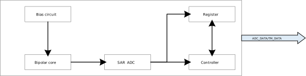
The thermal includes the following sub-modules:
Bias circuit
Generates bias current for bipolar core
Bipolar core
Generates temperature-dependent voltages
SAR ADC
12bits SAR ADC convert to 12 bits ADC code
Thermal is ch8 of SAR ADC
Controller
Controls and manages the interrupt
Controls low- temperature warning, high-temperature warning and over-temperature protection
Register
Contains configuration registers, result registers, interrupt registers
The interface to software

