Functional Description
Channel Switch List
The ADC provides a mechanism that allows software to configure the complete conversion sequence via an ADC channel switch list. Software can specify the target channel numbers to be converted with two registers (REG_ADC_CHSW_LIST_0 and REG_ADC_CHSW_LIST_1). The list length field in the REG_ADC_CONF[7:4] register can be configured to configure the number of channels in the sequence.
For example, consider the values configured for REG_ADC_CHSW_LIST_0 and REG_ADC_CHSW_LIST_1 as shown in the following table:
Register |
[3:0] |
[7:4] |
[11:8] |
[15:12] |
[19:16] |
[23:20] |
[27:24] |
[31:28] |
|---|---|---|---|---|---|---|---|---|
REG_ADC_CHSW_LIST_0 |
0 |
1 |
2 |
3 |
4 |
5 |
9 |
0 |
REG_ADC_CHSW_LIST_1 |
1 |
9 |
5 |
4 |
3 |
2 |
1 |
0 |
If REG_ADC_CONF[7:4] is set to 9, the ADC converts only the first 10 (the value of REG_ADC_CONF[7:4] + 1) channels in the list. When operating in Auto mode, the ADC performs conversions sequentially from the first channel to the last channel specified in the list. Once the channel length count reaches the value configured in REG_ADC_CONF[7:4], the ADC restarts the conversion sequence from the first channel (as illustrated in the following figure).

Auto mode waveform
The REG_ADC_LAST_CH[3:0] field indicates the last converted channel, which helps in tracking the current position within the sequence. Additionally, the REG_ADC_BUSY_STS[0] bit indicates the ADC’s busy status; it remains 1 while the ADC is actively processing a channel conversion.
Operation Mode
Ameba supports only one operation mode: auto mode.
Auto Mode
In auto mode, ADC continuously executes conversions without any trigger sources after auto channel switch register is set. Auto mode would not stop conversions until auto channel switch register is clear (register REG_ADC_AUTO_CSW_CTRL [0]) or the auto channel switch is disabled (register REG_ADC_CONF[3:1]).
In auto mode, ADC samples automatically by hardware without assistance of core or other modules, it can be applied to the situation where core resources are limited and real-time detection is required. Refer to Auto mode waveform for the auto mode waveform.
The ADC will scan the channels in the list in order. There is no interval between the adjacent channels, and the scanning speed only depends on the sampling rate of the ADC. At the end of the sampling period, the ADC immediately outputs the data to register and FIFO. So there is no need to set the CH switching time and settling time.
Because the sampled data is continuously filled into the register and FIFO when the REG_ADC_AUTO_CSW_CTRL [0] is set, if the data cannot be taken out, the data will be lost and the overflowed data will not be filled into the FIFO. For intermittent data getting from FIFO, FIFO clearing is recommended before getting.
However, there is a situation that needs to be paid attention to: if the internal resistance of the signal source sampled by ADC is very large, the input signal is easy to receive interference.

The solution is as follows:
Reduce the impedance
As shown in the following figure, operational amplifier (OA) provides extremely low output impedance.

Arrange Grounding Isolation Channel in channel list
As shown in the following figure, using a GND channel (internal GND channel or external channel which is connected to GND), configure the channel list of ADC to: CH0, CH_GND, CH1, CH_GND, CH2 … CH5, CH_GND. This avoids crosstalk, and the resulting inter-channel delay depends on the sampling rate of the ADC and the configuration of the channel list.

Ameba supports three different operation modes: auto mode, timer-trigger mode, and software-trigger mode.
Although various modes are available to meet specific requirements, only one operation mode can be active at a time. All modes execute conversions based on the channel switch list. The primary distinction between these operation modes lies in the trigger source, which drives the ADC module to perform conversions.
Auto Mode
In auto mode, ADC continuously executes conversions without any trigger sources after auto channel switch register is set. Auto mode would not stop conversions until auto channel switch register is clear (register REG_ADC_AUTO_CSW_CTRL [0]) or the auto channel switch is disabled (register REG_ADC_CONF[3:1]).
In auto mode, ADC samples automatically by hardware without assistance of core or other modules, it can be applied to the situation where core resources are limited and real-time detection is required. Refer to Auto mode waveform for the auto mode waveform.
The ADC will scan the channels in the list in order. There is no interval between the adjacent channels, and the scanning speed only depends on the sampling rate of the ADC. At the end of the sampling period, the ADC immediately outputs the data to register and FIFO. So there is no need to set the CH switching time and settling time.
Because the sampled data is continuously filled into the register and FIFO when the REG_ADC_AUTO_CSW_CTRL [0] is set, if the data cannot be taken out, the data will be lost and the overflowed data will not be filled into the FIFO. For intermittent data getting from FIFO, FIFO clearing is recommended before getting.
However, there is a situation that needs to be paid attention to: if the internal resistance of the signal source sampled by ADC is very large, the input signal is easy to receive interference.
The solution is as follows:
Reduce the impedance
As shown in the following figure, operational amplifier (OA) provides extremely low output impedance.
Arrange Grounding Isolation Channel in channel list
As shown in the following figure, using a GND channel (internal GND channel or external channel which is connected to GND), configure the channel list of ADC to: CH0, CH_GND, CH1, CH_GND, CH2 … CH5, CH_GND. This avoids crosstalk, and the resulting inter-channel delay depends on the sampling rate of the ADC and the configuration of the channel list.
Timer-trigger Mode
In timer-trigger mode, ADC can cooperate with timer modules to do conversions. System software sets timer trigger control register to enable timer module and set an appropriate timer event period. After that, ADC do one conversions when one timer event occurs based on system design.
Same as auto mode, the timer-trigger mode can work independently without system software, which means it can reduce the core resources partly. What’s more, ADC can automatically go to shut down mode between two timer trigger events that can largely reduce the ADC power consumption itself. Refer to the following figure for the timer-trigger mode waveform.

After each trigger, ADC will power on and perform the sampling conversion, and immediately store the results in the register and FIFO, after which ADC will power down. Until the next trigger signal arrives, ADC will re-power on and perform the entire list channel sampling conversion.
Therefore, the interval time between adjacent trigger is limited by the power-on time of ADC, and the recommended interval is not less than 1ms. Sampling during the power-on of ADC is not complete, which may result in data errors. After power-on, ADC starts sampling immediately, and the sampling period is determined by the sampling rate.
Same as auto mode, at the end of the sampling period, the ADC immediately outputs the data to register and FIFO.
Note
The current IC supports up to 8 timer sources (timer 0~7).
Every time trigger source is generated, only one channel in the channel list will be sampled.
Software-trigger Mode
The software-trigger mode is similar with timer-trigger mode, and the difference between them is the trigger source. For general usage, system software tends to handle ADC conversion timing. Every time software trigger register (REG_ADC_SW_TRIG[0]) is set, ADC module performs channel sampling conversion. System software checks ready/busy register (REG_ADC_BUSY_STS[0]) before reading conversion data register (REG_ADC_DATA_GLOBAL).
Compared with timer-trigger mode, this mode is more flexible. Software can manually trigger ADC sampling according to the actual situation, and the trigger time is not fixed. Refer to the following figure for the software-trigger mode waveform.

Similar to timer-trigger mode, between every two triggers, ADC enters the sleep state, and the trigger needs to be re-power on. As a result, the trigger interval should not be too short. It is recommended that the trigger interval should not be less than 1ms.
Note
Every time trigger source is generated, only one channel in the channel list will be sampled.
Summary
The following table shows the differences and applications of different operation modes.
Operation mode |
Configuration |
Difference |
Applications |
|---|---|---|---|
Auto mode |
REG_ADC_CONF[3:1] = 1 |
|
The case that needs real-time detection and more consumption. |
Timer-trigger mode |
REG_ADC_CONF[3:1] = 2 |
|
The case that needs periodic monitoring and less consumption. |
Software-trigger mode |
REG_ADC_CONF[3:1] = 0 REG_ADC_SW_TRIG[0] = 1 |
Need software but be more flexible |
The case that flexibly triggers ADC according to the current environment. |
Ameba supports three different operation modes: auto mode, timer-trigger mode, and software-trigger mode.
Although various modes are available to meet specific requirements, only one operation mode can be active at a time. All modes execute conversions based on the channel switch list. The primary distinction between these operation modes lies in the trigger source, which drives the ADC module to perform conversions.
Auto Mode
In auto mode, ADC continuously executes conversions without any trigger sources after auto channel switch register is set. Auto mode would not stop conversions until auto channel switch register is clear (register REG_ADC_AUTO_CSW_CTRL [0]) or the auto channel switch is disabled (register REG_ADC_CONF[3:1]).
In auto mode, ADC samples automatically by hardware without assistance of core or other modules, it can be applied to the situation where core resources are limited and real-time detection is required. Refer to Auto mode waveform for the auto mode waveform.
The ADC will scan the channels in the list in order. There is no interval between the adjacent channels, and the scanning speed only depends on the sampling rate of the ADC. At the end of the sampling period, the ADC immediately outputs the data to register and FIFO. So there is no need to set the CH switching time and settling time.
Because the sampled data is continuously filled into the register and FIFO when the REG_ADC_AUTO_CSW_CTRL [0] is set, if the data cannot be taken out, the data will be lost and the overflowed data will not be filled into the FIFO. For intermittent data getting from FIFO, FIFO clearing is recommended before getting.
However, there is a situation that needs to be paid attention to: if the internal resistance of the signal source sampled by ADC is very large, the input signal is easy to receive interference.
The solution is as follows:
Reduce the impedance
As shown in the following figure, operational amplifier (OA) provides extremely low output impedance.
Arrange Grounding Isolation Channel in channel list
As shown in the following figure, using a GND channel (internal GND channel or external channel which is connected to GND), configure the channel list of ADC to: CH0, CH_GND, CH1, CH_GND, CH2 … CH5, CH_GND. This avoids crosstalk, and the resulting inter-channel delay depends on the sampling rate of the ADC and the configuration of the channel list.
Timer-trigger Mode
In timer-trigger mode, ADC can cooperate with timer modules to do conversions. System software sets timer trigger control register to enable timer module and set an appropriate timer event period. After that, ADC do one conversions when one timer event occurs based on system design.
Same as auto mode, the timer-trigger mode can work independently without system software, which means it can reduce the core resources partly. What’s more, ADC can automatically go to shut down mode between two timer trigger events that can largely reduce the ADC power consumption itself. Refer to the following figure for the timer-trigger mode waveform.
After each trigger, ADC will power on and perform the sampling conversion, and immediately store the results in the register and FIFO, after which ADC will power down. Until the next trigger signal arrives, ADC will re-power on and perform the entire list channel sampling conversion.
Therefore, the interval time between adjacent trigger is limited by the power-on time of ADC, and the recommended interval is not less than 1ms. Sampling during the power-on of ADC is not complete, which may result in data errors. After power-on, ADC starts sampling immediately, and the sampling period is determined by the sampling rate.
Same as auto mode, at the end of the sampling period, the ADC immediately outputs the data to register and FIFO.
Note
The current IC supports up to 8 timer sources (timer 0~7).
Every time trigger source is generated, only one channel in the channel list will be sampled.
Software-trigger Mode
The software-trigger mode is similar with timer-trigger mode, and the difference between them is the trigger source. For general usage, system software tends to handle ADC conversion timing. Every time software trigger register (REG_ADC_SW_TRIG[0]) is set, ADC module performs channel sampling conversion. System software checks ready/busy register (REG_ADC_BUSY_STS[0]) before reading conversion data register (REG_ADC_DATA_GLOBAL).
Compared with timer-trigger mode, this mode is more flexible. Software can manually trigger ADC sampling according to the actual situation, and the trigger time is not fixed. Refer to the following figure for the software-trigger mode waveform.
Similar to timer-trigger mode, between every two triggers, ADC enters the sleep state, and the trigger needs to be re-power on. As a result, the trigger interval should not be too short. It is recommended that the trigger interval should not be less than 1ms.
Note
Every time trigger source is generated, only one channel in the channel list will be sampled.
Summary
The following table shows the differences and applications of different operation modes.
Operation mode |
Configuration |
Difference |
Applications |
|---|---|---|---|
Auto mode |
REG_ADC_CONF[3:1] = 1 |
|
The case that needs real-time detection and more consumption. |
Timer-trigger mode |
REG_ADC_CONF[3:1] = 2 |
|
The case that needs periodic monitoring and less consumption. |
Software-trigger mode |
REG_ADC_CONF[3:1] = 0 REG_ADC_SW_TRIG[0] = 1 |
Need software but be more flexible |
The case that flexibly triggers ADC according to the current environment. |
Ameba supports three different operation modes: auto mode, timer-trigger mode, and software-trigger mode.
Although various modes are available to meet specific requirements, only one operation mode can be active at a time. All modes execute conversions based on the channel switch list. The primary distinction between these operation modes lies in the trigger source, which drives the ADC module to perform conversions.
Auto Mode
In auto mode, ADC continuously executes conversions without any trigger sources after auto channel switch register is set. Auto mode would not stop conversions until auto channel switch register is clear (register REG_ADC_AUTO_CSW_CTRL [0]) or the auto channel switch is disabled (register REG_ADC_CONF[3:1]).
In auto mode, ADC samples automatically by hardware without assistance of core or other modules, it can be applied to the situation where core resources are limited and real-time detection is required. Refer to Auto mode waveform for the auto mode waveform.
The ADC will scan the channels in the list in order. There is no interval between the adjacent channels, and the scanning speed only depends on the sampling rate of the ADC. At the end of the sampling period, the ADC immediately outputs the data to register and FIFO. So there is no need to set the CH switching time and settling time.
Because the sampled data is continuously filled into the register and FIFO when the REG_ADC_AUTO_CSW_CTRL [0] is set, if the data cannot be taken out, the data will be lost and the overflowed data will not be filled into the FIFO. For intermittent data getting from FIFO, FIFO clearing is recommended before getting.
However, there is a situation that needs to be paid attention to: if the internal resistance of the signal source sampled by ADC is very large, the input signal is easy to receive interference.
The solution is as follows:
Reduce the impedance
As shown in the following figure, operational amplifier (OA) provides extremely low output impedance.
Arrange Grounding Isolation Channel in channel list
As shown in the following figure, using a GND channel (internal GND channel or external channel which is connected to GND), configure the channel list of ADC to: CH0, CH_GND, CH1, CH_GND, CH2 … CH5, CH_GND. This avoids crosstalk, and the resulting inter-channel delay depends on the sampling rate of the ADC and the configuration of the channel list.
Timer-trigger Mode
In timer-trigger mode, ADC can cooperate with timer modules to do conversions. System software sets timer trigger control register to enable timer module and set an appropriate timer event period. After that, ADC do one conversions when one timer event occurs based on system design.
Same as auto mode, the timer-trigger mode can work independently without system software, which means it can reduce the core resources partly. What’s more, ADC can automatically go to shut down mode between two timer trigger events that can largely reduce the ADC power consumption itself. Refer to the following figure for the timer-trigger mode waveform.
After each trigger, ADC will power on and perform the sampling conversion, and immediately store the results in the register and FIFO, after which ADC will power down. Until the next trigger signal arrives, ADC will re-power on and perform the entire list channel sampling conversion.
Therefore, the interval time between adjacent trigger is limited by the power-on time of ADC, and the recommended interval is not less than 1ms. Sampling during the power-on of ADC is not complete, which may result in data errors. After power-on, ADC starts sampling immediately, and the sampling period is determined by the sampling rate.
Same as auto mode, at the end of the sampling period, the ADC immediately outputs the data to register and FIFO.
Note
The current IC supports up to 8 timer sources (timer 0~7).
Every time trigger source is generated, only one channel in the channel list will be sampled.
Software-trigger Mode
The software-trigger mode is similar with timer-trigger mode, and the difference between them is the trigger source. For general usage, system software tends to handle ADC conversion timing. Every time software trigger register (REG_ADC_SW_TRIG[0]) is set, ADC module performs channel sampling conversion. System software checks ready/busy register (REG_ADC_BUSY_STS[0]) before reading conversion data register (REG_ADC_DATA_GLOBAL).
Compared with timer-trigger mode, this mode is more flexible. Software can manually trigger ADC sampling according to the actual situation, and the trigger time is not fixed. Refer to the following figure for the software-trigger mode waveform.
Similar to timer-trigger mode, between every two triggers, ADC enters the sleep state, and the trigger needs to be re-power on. As a result, the trigger interval should not be too short. It is recommended that the trigger interval should not be less than 1ms.
Note
Every time trigger source is generated, only one channel in the channel list will be sampled.
Summary
The following table shows the differences and applications of different operation modes.
Operation mode |
Configuration |
Difference |
Applications |
|---|---|---|---|
Auto mode |
REG_ADC_CONF[3:1] = 1 |
|
The case that needs real-time detection and more consumption. |
Timer-trigger mode |
REG_ADC_CONF[3:1] = 2 |
|
The case that needs periodic monitoring and less consumption. |
Software-trigger mode |
REG_ADC_CONF[3:1] = 0 REG_ADC_SW_TRIG[0] = 1 |
Need software but be more flexible |
The case that flexibly triggers ADC according to the current environment. |
Ameba supports three different operation modes: auto mode, timer-trigger mode, and software-trigger mode.
Although various modes are available to meet specific requirements, only one operation mode can be active at a time. All modes execute conversions based on the channel switch list. The primary distinction between these operation modes lies in the trigger source, which drives the ADC module to perform conversions.
Auto Mode
In auto mode, ADC continuously executes conversions without any trigger sources after auto channel switch register is set. Auto mode would not stop conversions until auto channel switch register is clear (register REG_ADC_AUTO_CSW_CTRL [0]) or the auto channel switch is disabled (register REG_ADC_CONF[3:1]).
In auto mode, ADC samples automatically by hardware without assistance of core or other modules, it can be applied to the situation where core resources are limited and real-time detection is required. Refer to Auto mode waveform for the auto mode waveform.
The ADC will scan the channels in the list in order. There is no interval between the adjacent channels, and the scanning speed only depends on the sampling rate of the ADC. At the end of the sampling period, the ADC immediately outputs the data to register and FIFO. So there is no need to set the CH switching time and settling time.
Because the sampled data is continuously filled into the register and FIFO when the REG_ADC_AUTO_CSW_CTRL [0] is set, if the data cannot be taken out, the data will be lost and the overflowed data will not be filled into the FIFO. For intermittent data getting from FIFO, FIFO clearing is recommended before getting.
However, there is a situation that needs to be paid attention to: if the internal resistance of the signal source sampled by ADC is very large, the input signal is easy to receive interference.
The solution is as follows:
Reduce the impedance
As shown in the following figure, operational amplifier (OA) provides extremely low output impedance.
Arrange Grounding Isolation Channel in channel list
As shown in the following figure, using a GND channel (internal GND channel or external channel which is connected to GND), configure the channel list of ADC to: CH0, CH_GND, CH1, CH_GND, CH2 … CH5, CH_GND. This avoids crosstalk, and the resulting inter-channel delay depends on the sampling rate of the ADC and the configuration of the channel list.
Timer-trigger Mode
In timer-trigger mode, ADC can cooperate with timer modules to do conversions. System software sets timer trigger control register to enable timer module and set an appropriate timer event period. After that, ADC do one conversions when one timer event occurs based on system design.
Same as auto mode, the timer-trigger mode can work independently without system software, which means it can reduce the core resources partly. What’s more, ADC can automatically go to shut down mode between two timer trigger events that can largely reduce the ADC power consumption itself. Refer to the following figure for the timer-trigger mode waveform.
After each trigger, ADC will power on and perform the sampling conversion, and immediately store the results in the register and FIFO, after which ADC will power down. Until the next trigger signal arrives, ADC will re-power on and perform the entire list channel sampling conversion.
Therefore, the interval time between adjacent trigger is limited by the power-on time of ADC, and the recommended interval is not less than 1ms. Sampling during the power-on of ADC is not complete, which may result in data errors. After power-on, ADC starts sampling immediately, and the sampling period is determined by the sampling rate.
Same as auto mode, at the end of the sampling period, the ADC immediately outputs the data to register and FIFO.
Note
The current IC supports up to 8 timer sources (timer 0~7).
Every time trigger source is generated, only one channel in the channel list will be sampled.
Software-trigger Mode
The software-trigger mode is similar with timer-trigger mode, and the difference between them is the trigger source. For general usage, system software tends to handle ADC conversion timing. Every time software trigger register (REG_ADC_SW_TRIG[0]) is set, ADC module performs channel sampling conversion. System software checks ready/busy register (REG_ADC_BUSY_STS[0]) before reading conversion data register (REG_ADC_DATA_GLOBAL).
Compared with timer-trigger mode, this mode is more flexible. Software can manually trigger ADC sampling according to the actual situation, and the trigger time is not fixed. Refer to the following figure for the software-trigger mode waveform.
Similar to timer-trigger mode, between every two triggers, ADC enters the sleep state, and the trigger needs to be re-power on. As a result, the trigger interval should not be too short. It is recommended that the trigger interval should not be less than 1ms.
Note
Every time trigger source is generated, only one channel in the channel list will be sampled.
Summary
The following table shows the differences and applications of different operation modes.
Operation mode |
Configuration |
Difference |
Applications |
|---|---|---|---|
Auto mode |
REG_ADC_CONF[3:1] = 1 |
|
The case that needs real-time detection and more consumption. |
Timer-trigger mode |
REG_ADC_CONF[3:1] = 2 |
|
The case that needs periodic monitoring and less consumption. |
Software-trigger mode |
REG_ADC_CONF[3:1] = 0 REG_ADC_SW_TRIG[0] = 1 |
Need software but be more flexible |
The case that flexibly triggers ADC according to the current environment. |
Ameba supports three different operation modes: auto mode, timer-trigger mode, and software-trigger mode.
Although various modes are available to meet specific requirements, only one operation mode can be active at a time. All modes execute conversions based on the channel switch list. The primary distinction between these operation modes lies in the trigger source, which drives the ADC module to perform conversions.
Auto Mode
In auto mode, ADC continuously executes conversions without any trigger sources after auto channel switch register is set. Auto mode would not stop conversions until auto channel switch register is clear (register REG_ADC_AUTO_CSW_CTRL [0]) or the auto channel switch is disabled (register REG_ADC_CONF[3:1]).
In auto mode, ADC samples automatically by hardware without assistance of core or other modules, it can be applied to the situation where core resources are limited and real-time detection is required. Refer to Auto mode waveform for the auto mode waveform.
The ADC will scan the channels in the list in order. There is no interval between the adjacent channels, and the scanning speed only depends on the sampling rate of the ADC. At the end of the sampling period, the ADC immediately outputs the data to register and FIFO. So there is no need to set the CH switching time and settling time.
Because the sampled data is continuously filled into the register and FIFO when the REG_ADC_AUTO_CSW_CTRL [0] is set, if the data cannot be taken out, the data will be lost and the overflowed data will not be filled into the FIFO. For intermittent data getting from FIFO, FIFO clearing is recommended before getting.
However, there is a situation that needs to be paid attention to: if the internal resistance of the signal source sampled by ADC is very large, the input signal is easy to receive interference.
The solution is as follows:
Reduce the impedance
As shown in the following figure, operational amplifier (OA) provides extremely low output impedance.
Arrange Grounding Isolation Channel in channel list
As shown in the following figure, using a GND channel (internal GND channel or external channel which is connected to GND), configure the channel list of ADC to: CH0, CH_GND, CH1, CH_GND, CH2 … CH5, CH_GND. This avoids crosstalk, and the resulting inter-channel delay depends on the sampling rate of the ADC and the configuration of the channel list.
Timer-trigger Mode
In timer-trigger mode, ADC can cooperate with timer modules to do conversions. System software sets timer trigger control register to enable timer module and set an appropriate timer event period. After that, ADC do one conversions when one timer event occurs based on system design.
Same as auto mode, the timer-trigger mode can work independently without system software, which means it can reduce the core resources partly. What’s more, ADC can automatically go to shut down mode between two timer trigger events that can largely reduce the ADC power consumption itself. Refer to the following figure for the timer-trigger mode waveform.
After each trigger, ADC will power on and perform the sampling conversion, and immediately store the results in the register and FIFO, after which ADC will power down. Until the next trigger signal arrives, ADC will re-power on and perform the entire list channel sampling conversion.
Therefore, the interval time between adjacent trigger is limited by the power-on time of ADC, and the recommended interval is not less than 1ms. Sampling during the power-on of ADC is not complete, which may result in data errors. After power-on, ADC starts sampling immediately, and the sampling period is determined by the sampling rate.
Same as auto mode, at the end of the sampling period, the ADC immediately outputs the data to register and FIFO.
Note
The current IC supports up to 8 timer sources (timer 0~7).
Every time trigger source is generated, only one channel in the channel list will be sampled.
Software-trigger Mode
The software-trigger mode is similar with timer-trigger mode, and the difference between them is the trigger source. For general usage, system software tends to handle ADC conversion timing. Every time software trigger register (REG_ADC_SW_TRIG[0]) is set, ADC module performs channel sampling conversion. System software checks ready/busy register (REG_ADC_BUSY_STS[0]) before reading conversion data register (REG_ADC_DATA_GLOBAL).
Compared with timer-trigger mode, this mode is more flexible. Software can manually trigger ADC sampling according to the actual situation, and the trigger time is not fixed. Refer to the following figure for the software-trigger mode waveform.
Similar to timer-trigger mode, between every two triggers, ADC enters the sleep state, and the trigger needs to be re-power on. As a result, the trigger interval should not be too short. It is recommended that the trigger interval should not be less than 1ms.
Note
Every time trigger source is generated, only one channel in the channel list will be sampled.
Summary
The following table shows the differences and applications of different operation modes.
Operation mode |
Configuration |
Difference |
Applications |
|---|---|---|---|
Auto mode |
REG_ADC_CONF[3:1] = 1 |
|
The case that needs real-time detection and more consumption. |
Timer-trigger mode |
REG_ADC_CONF[3:1] = 2 |
|
The case that needs periodic monitoring and less consumption. |
Software-trigger mode |
REG_ADC_CONF[3:1] = 0 REG_ADC_SW_TRIG[0] = 1 |
Need software but be more flexible |
The case that flexibly triggers ADC according to the current environment. |
Ameba supports three different operation modes: auto mode, timer-trigger mode, and software-trigger mode.
Although various modes are available to meet specific requirements, only one operation mode can be active at a time. All modes execute conversions based on the channel switch list. The primary distinction between these operation modes lies in the trigger source, which drives the ADC module to perform conversions.
Auto Mode
In auto mode, ADC continuously executes conversions without any trigger sources after auto channel switch register is set. Auto mode would not stop conversions until auto channel switch register is clear (register REG_ADC_AUTO_CSW_CTRL [0]) or the auto channel switch is disabled (register REG_ADC_CONF[3:1]).
In auto mode, ADC samples automatically by hardware without assistance of core or other modules, it can be applied to the situation where core resources are limited and real-time detection is required. Refer to Auto mode waveform for the auto mode waveform.
The ADC will scan the channels in the list in order. There is no interval between the adjacent channels, and the scanning speed only depends on the sampling rate of the ADC. At the end of the sampling period, the ADC immediately outputs the data to register and FIFO. So there is no need to set the CH switching time and settling time.
Because the sampled data is continuously filled into the register and FIFO when the REG_ADC_AUTO_CSW_CTRL [0] is set, if the data cannot be taken out, the data will be lost and the overflowed data will not be filled into the FIFO. For intermittent data getting from FIFO, FIFO clearing is recommended before getting.
However, there is a situation that needs to be paid attention to: if the internal resistance of the signal source sampled by ADC is very large, the input signal is easy to receive interference.
The solution is as follows:
Reduce the impedance
As shown in the following figure, operational amplifier (OA) provides extremely low output impedance.
Arrange Grounding Isolation Channel in channel list
As shown in the following figure, using a GND channel (internal GND channel or external channel which is connected to GND), configure the channel list of ADC to: CH0, CH_GND, CH1, CH_GND, CH2 … CH5, CH_GND. This avoids crosstalk, and the resulting inter-channel delay depends on the sampling rate of the ADC and the configuration of the channel list.
Note
If CH14(internal GND channel) is filled into the list as a channel, the output of CH14 (which remains 0) will not be stored in FIFO, so users can easily obtain sample data of other channels from FIFO.
Timer-trigger Mode
In timer-trigger mode, ADC can cooperate with timer modules to do conversions. System software sets timer trigger control register to enable timer module and set an appropriate timer event period. After that, ADC do one conversions when one timer event occurs based on system design.
Same as auto mode, the timer-trigger mode can work independently without system software, which means it can reduce the core resources partly. What’s more, ADC can automatically go to shut down mode between two timer trigger events that can largely reduce the ADC power consumption itself. Refer to the following figure for the timer-trigger mode waveform.
After each trigger, ADC will power on and perform the sampling conversion, and immediately store the results in the register and FIFO, after which ADC will power down. Until the next trigger signal arrives, ADC will re-power on and perform the entire list channel sampling conversion.
Therefore, the interval time between adjacent trigger is limited by the power-on time of ADC, and the recommended interval is not less than 1ms. Sampling during the power-on of ADC is not complete, which may result in data errors. After power-on, ADC starts sampling immediately, and the sampling period is determined by the sampling rate.
Same as auto mode, at the end of the sampling period, the ADC immediately outputs the data to register and FIFO.
Note
The current IC supports up to 4 timer sources (timer 0~3).
Every time trigger source is generated, all the channels in the channel list will be sampled.
Software-trigger Mode
The software-trigger mode is similar with timer-trigger mode, and the difference between them is the trigger source. For general usage, system software tends to handle ADC conversion timing. Every time software trigger register (REG_ADC_SW_TRIG[0]) is set, ADC module performs channel sampling conversion. System software checks ready/busy register (REG_ADC_BUSY_STS[0]) before reading conversion data register (REG_ADC_DATA_GLOBAL).
Compared with timer-trigger mode, this mode is more flexible. Software can manually trigger ADC sampling according to the actual situation, and the trigger time is not fixed. Refer to the following figure for the software-trigger mode waveform.
Similar to timer-trigger mode, between every two triggers, ADC enters the sleep state, and the trigger needs to be re-power on. As a result, the trigger interval should not be too short. It is recommended that the trigger interval should not be less than 1ms.
Note
Every time trigger source is generated, all the channels in the channel list will be sampled.
Summary
The following table shows the differences and applications of different operation modes.
Operation mode |
Configuration |
Difference |
Applications |
|---|---|---|---|
Auto mode |
REG_ADC_CONF[3:1] = 1 |
|
The case that needs real-time detection and more consumption. |
Timer-trigger mode |
REG_ADC_CONF[3:1] = 2 |
|
The case that needs periodic monitoring and less consumption. |
Software-trigger mode |
REG_ADC_CONF[3:1] = 0 REG_ADC_SW_TRIG[0] = 1 |
Need software but be more flexible |
The case that flexibly triggers ADC according to the current environment. |
Ameba supports three different operation modes: auto mode, timer-trigger mode, and software-trigger mode.
Although various modes are available to meet specific requirements, only one operation mode can be active at a time. All modes execute conversions based on the channel switch list. The primary distinction between these operation modes lies in the trigger source, which drives the ADC module to perform conversions.
Auto Mode
In auto mode, ADC continuously executes conversions without any trigger sources after auto channel switch register is set. Auto mode would not stop conversions until auto channel switch register is clear (register REG_ADC_AUTO_CSW_CTRL [0]) or the auto channel switch is disabled (register REG_ADC_CONF[3:1]).
In auto mode, ADC samples automatically by hardware without assistance of core or other modules, it can be applied to the situation where core resources are limited and real-time detection is required. Refer to Auto mode waveform for the auto mode waveform.
The ADC will scan the channels in the list in order. There is no interval between the adjacent channels, and the scanning speed only depends on the sampling rate of the ADC. At the end of the sampling period, the ADC immediately outputs the data to register and FIFO. So there is no need to set the CH switching time and settling time.
Because the sampled data is continuously filled into the register and FIFO when the REG_ADC_AUTO_CSW_CTRL [0] is set, if the data cannot be taken out, the data will be lost and the overflowed data will not be filled into the FIFO. For intermittent data getting from FIFO, FIFO clearing is recommended before getting.
However, there is a situation that needs to be paid attention to: if the internal resistance of the signal source sampled by ADC is very large, the input signal is easy to receive interference.
The solution is as follows:
Reduce the impedance
As shown in the following figure, operational amplifier (OA) provides extremely low output impedance.
Arrange Grounding Isolation Channel in channel list
As shown in the following figure, using a GND channel (internal GND channel or external channel which is connected to GND), configure the channel list of ADC to: CH0, CH_GND, CH1, CH_GND, CH2 … CH5, CH_GND. This avoids crosstalk, and the resulting inter-channel delay depends on the sampling rate of the ADC and the configuration of the channel list.
Arrange Grounding Isolation Channel in conversion time
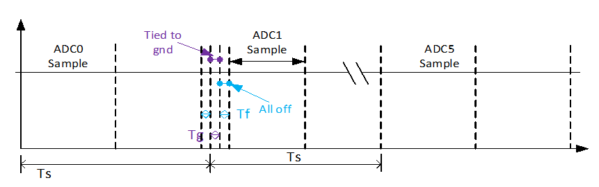
As shown in the following figure,each channel adds a bit to control whether the ISO channel is selected, and also adds a corresponding selection time configuration: a) Select ISO ch9, selection time Tg is configurable,Related to path capacitors and resistors, default value 100ns, adjustable settings b) All off (no channel selected), selection time Tf set to 25ns
Note
If CH9(internal GND channel) is filled into the list as a channel, the output of CH9 (which remains 0) will not be stored in FIFO, so users can easily obtain sample data of other channels from FIFO.
Timer-trigger Mode
In timer-trigger mode, ADC can cooperate with timer modules to do conversions. System software sets timer trigger control register to enable timer module and set an appropriate timer event period. After that, ADC do one conversions when one timer event occurs based on system design.
Same as auto mode, the timer-trigger mode can work independently without system software, which means it can reduce the core resources partly. What’s more, ADC can automatically go to shut down mode between two timer trigger events that can largely reduce the ADC power consumption itself. Refer to the following figure for the timer-trigger mode waveform.
After each trigger, ADC will power on and perform the sampling conversion, and immediately store the results in the register and FIFO, after which ADC will power down. Until the next trigger signal arrives, ADC will re-power on and perform the entire list channel sampling conversion.
Therefore, the interval time between adjacent trigger is limited by the power-on time of ADC, and the recommended interval is not less than 1ms. Sampling during the power-on of ADC is not complete, which may result in data errors. After power-on, ADC starts sampling immediately, and the sampling period is determined by the sampling rate.
Same as auto mode, at the end of the sampling period, the ADC immediately outputs the data to register and FIFO.
Note
The current IC supports up to 4 timer sources (timer 0~3).
Every time trigger source is generated, all the channels in the channel list will be sampled.
Software-trigger Mode
The software-trigger mode is similar with timer-trigger mode, and the difference between them is the trigger source. For general usage, system software tends to handle ADC conversion timing. Every time software trigger register (REG_ADC_SW_TRIG[0]) is set, ADC module performs channel sampling conversion. System software checks ready/busy register (REG_ADC_BUSY_STS[0]) before reading conversion data register (REG_ADC_DATA_GLOBAL).
Compared with timer-trigger mode, this mode is more flexible. Software can manually trigger ADC sampling according to the actual situation, and the trigger time is not fixed. Refer to the following figure for the software-trigger mode waveform.
Similar to timer-trigger mode, between every two triggers, ADC enters the sleep state, and the trigger needs to be re-power on. As a result, the trigger interval should not be too short. It is recommended that the trigger interval should not be less than 1ms.
Note
Every time trigger source is generated, all the channels in the channel list will be sampled.
Summary
The following table shows the differences and applications of different operation modes.
Operation mode |
Configuration |
Difference |
Applications |
|---|---|---|---|
Auto mode |
REG_ADC_CONF[3:1] = 1 |
|
The case that needs real-time detection and more consumption. |
Timer-trigger mode |
REG_ADC_CONF[3:1] = 2 |
|
The case that needs periodic monitoring and less consumption. |
Software-trigger mode |
REG_ADC_CONF[3:1] = 0 REG_ADC_SW_TRIG[0] = 1 |
Need software but be more flexible |
The case that flexibly triggers ADC according to the current environment. |
Low Power Clock Source
The following figure shows the ADC clock generation tree. Users can configure ADC sample frequency by setting register REG_ADC_CLK_DIV[2:0].

After the system enters the low-power state, the ADC can execute sampling operations via auto mode, and the system can be woken up by an ADC interrupt.
Under auto mode, the ADC hardware automatically and continuously samples the external analog voltage. Users can preset high/low thresholds as well as comparison criteria. The CPU remains completely in sleep mode throughout the entire process, and the system is woken up only when the sampled voltage meets the predefined comparison criteria.
In the low-power state, only OSC clock can be selected as the ADC clock, allowing the system to be woken up.
Note
Only auto mode is supported for low-power operation on this chip.
The following figure shows the ADC clock generation tree. Users can configure ADC sample frequency by setting register REG_ADC_CLK_DIV[2:0].
After the system enters the low-power state, the ADC can execute sampling operations via auto mode or timer-trigger mode, and the system can be woken up by an ADC interrupt.
Auto mode: The ADC hardware automatically and continuously samples the external analog voltage. Users can preset high/low thresholds as well as comparison criteria. The CPU remains completely in sleep mode throughout the entire process, and the system is woken up only when the sampled voltage meets the predefined comparison criteria.
Timer-trigger mode: In the low-power state, the timer periodically sends a signal to trigger the ADC to perform a sampling operation, and the system can be woken up upon the completion of the sampling.
In the low-power state, only OSC clock can be selected as the ADC clock, allowing the system to be woken up.
The following figure shows the ADC clock generation tree. Users can configure ADC sample frequency by setting register REG_ADC_CLK_DIV[2:0].
After the system enters the low-power state, the ADC can execute sampling operations via auto mode or timer-trigger mode, and the system can be woken up by an ADC interrupt.
Auto mode: The ADC hardware automatically and continuously samples the external analog voltage. Users can preset high/low thresholds as well as comparison criteria. The CPU remains completely in sleep mode throughout the entire process, and the system is woken up only when the sampled voltage meets the predefined comparison criteria.
Timer-trigger mode: In the low-power state, the timer periodically sends a signal to trigger the ADC to perform a sampling operation, and the system can be woken up upon the completion of the sampling.
In the low-power state, only OSC clock can be selected as the ADC clock, allowing the system to be woken up.
The following figure shows the ADC clock generation tree. Users can configure ADC sample frequency by setting register REG_ADC_CLK_DIV[2:0].
After the system enters the low-power state, the ADC can execute sampling operations via auto mode or timer-trigger mode, and the system can be woken up by an ADC interrupt.
Auto mode: The ADC hardware automatically and continuously samples the external analog voltage. Users can preset high/low thresholds as well as comparison criteria. The CPU remains completely in sleep mode throughout the entire process, and the system is woken up only when the sampled voltage meets the predefined comparison criteria.
Timer-trigger mode: In the low-power state, the timer periodically sends a signal to trigger the ADC to perform a sampling operation, and the system can be woken up upon the completion of the sampling.
In the low-power state, only OSC clock can be selected as the ADC clock, allowing the system to be woken up.
The following figure shows the ADC clock generation tree. Users can configure ADC sample frequency by setting register REG_ADC_CLK_DIV[2:0].
After the system enters the low-power state, the ADC can execute sampling operations via auto mode or timer-trigger mode, and the system can be woken up by an ADC interrupt.
Auto mode: The ADC hardware automatically and continuously samples the external analog voltage. Users can preset high/low thresholds as well as comparison criteria. The CPU remains completely in sleep mode throughout the entire process, and the system is woken up only when the sampled voltage meets the predefined comparison criteria.
Timer-trigger mode: In the low-power state, the timer periodically sends a signal to trigger the ADC to perform a sampling operation, and the system can be woken up upon the completion of the sampling.
In the low-power state, only OSC clock can be selected as the ADC clock, allowing the system to be woken up.
The following figure shows the ADC clock generation tree. Users can configure ADC sample frequency by setting register REG_ADC_CLK_DIV[2:0].
After the system enters the low-power state, the ADC can execute sampling operations via auto mode or timer-trigger mode, and the system can be woken up by an ADC interrupt.
Auto mode: The ADC hardware automatically and continuously samples the external analog voltage. Users can preset high/low thresholds as well as comparison criteria. The CPU remains completely in sleep mode throughout the entire process, and the system is woken up only when the sampled voltage meets the predefined comparison criteria.
Timer-trigger mode: In the low-power state, the timer periodically sends a signal to trigger the ADC to perform a sampling operation, and the system can be woken up upon the completion of the sampling.
In the low-power state, only OSC clock can be selected as the ADC clock, allowing the system to be woken up.
Note
To use OSC as the ADC clock, set keep_osc4m_on in ps_config to TRUE in ameba_sleepcfg.c.
The following figure shows the ADC clock generation tree. Users can configure both the sampling and conversion time of each channel by setting register REG_ADC_CLK_HCNTx and register REG_ADC_CLK_LCNT0_DIV. The ADC supports both OSC and XTAL clock sources; the XTAL clock offers higher performance, while the OSC clock consumes less power.

After the system enters the low-power state, the ADC can execute sampling operations via auto mode or timer-trigger mode, and the system can be woken up by an ADC interrupt.
Auto mode: The ADC hardware automatically and continuously samples the external analog voltage. Users can preset high/low thresholds as well as comparison criteria. The CPU remains completely in sleep mode throughout the entire process, and the system is woken up only when the sampled voltage meets the predefined comparison criteria.
Timer-trigger mode: In the low-power state, the timer periodically sends a signal to trigger the ADC to perform a sampling operation, and the system can be woken up upon the completion of the sampling.
In the low-power state, only OSC clock can be selected as the ADC clock, allowing the system to be woken up.
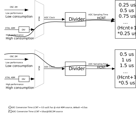
The following figure shows the ADC clock generation tree. Users can configure both the sampling and conversion time of each channel by setting register REG_ADC_CLK_HCNTx and register REG_ADC_CLK_LCNT0_DIV. The ADC supports both OSC and XTAL clock sources; the XTAL clock offers higher performance, while the OSC clock consumes less power.
After the system enters the low-power state, the ADC can execute sampling operations via auto mode or timer-trigger mode, and the system can be woken up by an ADC interrupt.
Auto mode: The ADC hardware automatically and continuously samples the external analog voltage. Users can preset high/low thresholds as well as comparison criteria. The CPU remains completely in sleep mode throughout the entire process, and the system is woken up only when the sampled voltage meets the predefined comparison criteria.
Timer-trigger mode: In the low-power state, the timer periodically sends a signal to trigger the ADC to perform a sampling operation, and the system can be woken up upon the completion of the sampling.
Independent Comparison Event of Each Channel
The voltage monitoring function can be realized by using ADC, and each CH of ADC can be configured with two independent comparison thresholds and different comparison criterion. When the sample value of ADC reaches the configured condition, an interrupt can be detected in REG_ADC_INTR_STS.
The threshold of each channel can be configured in REG_ADC_COMP_TH_CHx, which contains both high threshold and low threshold. The comparison criterion of each channel can be configured in REG_ADC_COMP_CTRL. ADC comparison supports four different comparison criterion:
Vin < bit_adc_comp_th_l_chx
Vin > bit_adc_comp_th_h_chx
Vin >= bit_adc_comp_th_l_chx and Vin <= bit_adc_comp_th_h_chx
Vin < bit_adc_comp_th_l_chx or Vin > bit_adc_comp_th_h_chx.
For example, when configured as Vin < bit_adc_comp_th_l_chx or Vin > bit_adc_comp_th_h_chx, if the ADC conversion data exceeds the higher and lower threshold, an interrupt event will occur.

Two different interrupt generation modes (level detection and edge detection) are used to inform CPU of comparison match events. The level detection mode continuously reports the interrupt, while the edge detection mode reports it only once when the interrupt is generated.
Two different interrupt generation modes (level detection and edge detection) are used to inform CPU of comparison match events. The level detection mode continuously reports the interrupt, while the edge detection mode reports it only once when the interrupt is generated.
Two different interrupt generation modes (level detection and edge detection) are used to inform CPU of comparison match events. The level detection mode continuously reports the interrupt, while the edge detection mode reports it only once when the interrupt is generated.
Two different interrupt generation modes (level detection and edge detection) are used to inform CPU of comparison match events. The level detection mode continuously reports the interrupt, while the edge detection mode reports it only once when the interrupt is generated.
Two different interrupt generation modes (level detection and edge detection) are used to inform CPU of comparison match events. The level detection mode continuously reports the interrupt, while the edge detection mode reports it only once when the interrupt is generated.
Level detection interrupt generation mode is used to inform CPU of comparison match events and it continuously reports the interrupt.
Two different interrupt generation modes (level detection and edge detection) are used to inform CPU of comparison match events. The level detection mode continuously reports the interrupt, while the edge detection mode reports it only once when the interrupt is generated.
Two different interrupt generation modes (level detection and edge detection) are used to inform CPU of comparison match events. The level detection mode continuously reports the interrupt, while the edge detection mode reports it only once when the interrupt is generated.
Acquisition of Sampling Results
FIFO
Users can easily acquire ADC sample results from the ADC FIFO by reading the REG_ADC_DATA_GLOBAL register. The ADC stores all sampled results within this FIFO. The ADC FIFO has 64 entries, and each 20-bit FIFO data entry consists of a 4-bit channel number and 16-bit conversion data, as shown in the following figure.

Because the FIFO acts as a buffer between the data acquisition and data processing systems operating at different speeds, timely data retrieval is crucial to prevent data loss.
During normal operation, the ADC continuously writes data to the FIFO, while the system reads from it. If the system reads data slower than the ADC writes it, a FIFO overflow will occur. In the event of an overflow, any newly sampled data is discarded and will not be written to the FIFO, as shown in the figure above.
Users can easily acquire ADC sample results from the ADC FIFO by reading the REG_ADC_DATA_GLOBAL register. The ADC stores all sampled results within this FIFO. The ADC FIFO has 64 entries, and each 16-bit FIFO data entry consists of a 4-bit channel number and 12-bit conversion data, as shown in the following figure.

Because the FIFO acts as a buffer between the data acquisition and data processing systems operating at different speeds, timely data retrieval is crucial to prevent data loss.
During normal operation, the ADC continuously writes data to the FIFO, while the system reads from it. If the system reads data slower than the ADC writes it, a FIFO overflow will occur. In the event of an overflow, any newly sampled data is discarded and will not be written to the FIFO, as shown in the figure above.
Users can easily acquire ADC sample results from the ADC FIFO by reading the REG_ADC_DATA_GLOBAL register. The ADC stores all sampled results within this FIFO. The ADC FIFO has 64 entries, and each 16-bit FIFO data entry consists of a 4-bit channel number and 12-bit conversion data, as shown in the following figure.
Because the FIFO acts as a buffer between the data acquisition and data processing systems operating at different speeds, timely data retrieval is crucial to prevent data loss.
During normal operation, the ADC continuously writes data to the FIFO, while the system reads from it. If the system reads data slower than the ADC writes it, a FIFO overflow will occur. In the event of an overflow, any newly sampled data is discarded and will not be written to the FIFO, as shown in the figure above.
Users can easily acquire ADC sample results from the ADC FIFO by reading the REG_ADC_DATA_GLOBAL register. The ADC stores all sampled results within this FIFO. The ADC FIFO has 64 entries, and each 16-bit FIFO data entry consists of a 4-bit channel number and 12-bit conversion data, as shown in the following figure.
Because the FIFO acts as a buffer between the data acquisition and data processing systems operating at different speeds, timely data retrieval is crucial to prevent data loss.
During normal operation, the ADC continuously writes data to the FIFO, while the system reads from it. If the system reads data slower than the ADC writes it, a FIFO overflow will occur. In the event of an overflow, any newly sampled data is discarded and will not be written to the FIFO, as shown in the figure above.
Users can easily acquire ADC sample results from the ADC FIFO by reading the REG_ADC_DATA_GLOBAL register. The ADC stores all sampled results within this FIFO. The ADC FIFO has 64 entries, and each 16-bit FIFO data entry consists of a 4-bit channel number and 12-bit conversion data, as shown in the following figure.
Because the FIFO acts as a buffer between the data acquisition and data processing systems operating at different speeds, timely data retrieval is crucial to prevent data loss.
During normal operation, the ADC continuously writes data to the FIFO, while the system reads from it. If the system reads data slower than the ADC writes it, a FIFO overflow will occur. In the event of an overflow, any newly sampled data is discarded and will not be written to the FIFO, as shown in the figure above.
Users can easily acquire ADC sample results from the ADC FIFO by reading the REG_ADC_DATA_GLOBAL register. The ADC stores all sampled results within this FIFO. The ADC FIFO has 64 entries, and each 16-bit FIFO data entry consists of a 4-bit channel number and 12-bit conversion data, as shown in the following figure.
Because the FIFO acts as a buffer between the data acquisition and data processing systems operating at different speeds, timely data retrieval is crucial to prevent data loss.
During normal operation, the ADC continuously writes data to the FIFO, while the system reads from it. If the system reads data slower than the ADC writes it, a FIFO overflow will occur. In the event of an overflow, any newly sampled data is discarded and will not be written to the FIFO, as shown in the figure above.
Users can easily acquire ADC sample results from the ADC FIFO by reading the REG_ADC_DATA_GLOBAL register. The ADC stores all sampled results within this FIFO. The ADC FIFO has 64 entries, and each 20-bit FIFO data entry consists of a 4-bit channel number and 16-bit conversion data, as shown in the following figure.
Because the FIFO acts as a buffer between the data acquisition and data processing systems operating at different speeds, timely data retrieval is crucial to prevent data loss.
During normal operation, the ADC continuously writes data to the FIFO, while the system reads from it. If the system reads data slower than the ADC writes it, a FIFO overflow will occur. In the event of an overflow, any newly sampled data is discarded and will not be written to the FIFO, as shown in the figure above.
Users can easily acquire ADC sample results from the ADC FIFO by reading the REG_ADC_DATA_GLOBAL register. The ADC stores all sampled results within this FIFO. The ADC FIFO has 64 entries, and each 20-bit FIFO data entry consists of a 4-bit channel number and 16-bit conversion data, as shown in the following figure.
Because the FIFO acts as a buffer between the data acquisition and data processing systems operating at different speeds, timely data retrieval is crucial to prevent data loss.
During normal operation, the ADC continuously writes data to the FIFO, while the system reads from it. If the system reads data slower than the ADC writes it, a FIFO overflow will occur. In the event of an overflow, any newly sampled data is discarded and will not be written to the FIFO, as shown in the figure above.
In addition to retrieving data promptly to avoid overflows, it is highly recommended to clear the ADC FIFO by setting REG_ADC_CLR_FIFO[0] before initiating any new data sampling process.
If the FIFO overflow interrupt (ADC_BIT_IT_FIFO_OVER_EN) is enabled, an interrupt signal is sent to the CPU NVIC upon a FIFO overflow. Similarly, if the FIFO empty interrupt (ADC_BIT_IT_FIFO_EMPTY_EN) is enabled, an interrupt is triggered when the FIFO becomes empty.
Additionally, users can set a custom FIFO full threshold by configuring REG_ADC_FULL_LVL[5:0]. When the FIFO full interrupt (ADC_BIT_IT_FIFO_FULL_EN) is enabled, an interrupt is sent to the CPU NVIC once the number of FIFO entries reaches this configured threshold, as shown in the following figure.
REG_ADC_FLR[5:0] indicates the current number of entries in the ADC FIFO.

Individual Channel Register
Each channel has its own data register to store its latest conversion result. These registers are named REG_ADC_DATA_CHx, where x represents the specific channel number (e.g., CH0).
REG_ADC_DATA_CHx[15:0] contains the latest conversion data for CHx.
REG_ADC_DATA_CHx[19:16] indicates the channel number associated with the latest conversion data.
REG_ADC_DATA_CHx[20] is a flag indicating a data overwrite event.
REG_ADC_DATA_CHx[21] is a flag indicating that a conversion is complete.
REG_ADC_DATA_CHx[11:0] contains the latest conversion data for CHx.
REG_ADC_DATA_CHx[15:12] indicates the channel number associated with the latest conversion data.
REG_ADC_DATA_CHx[16] is a flag indicating a data overwrite event.
REG_ADC_DATA_CHx[17] is a flag indicating that a conversion is complete.
REG_ADC_DATA_CHx[11:0] contains the latest conversion data for CHx.
REG_ADC_DATA_CHx[15:12] indicates the channel number associated with the latest conversion data.
REG_ADC_DATA_CHx[16] is a flag indicating a data overwrite event.
REG_ADC_DATA_CHx[17] is a flag indicating that a conversion is complete.
REG_ADC_DATA_CHx[11:0] contains the latest conversion data for CHx.
REG_ADC_DATA_CHx[15:12] indicates the channel number associated with the latest conversion data.
REG_ADC_DATA_CHx[16] is a flag indicating a data overwrite event.
REG_ADC_DATA_CHx[17] is a flag indicating that a conversion is complete.
REG_ADC_DATA_CHx[11:0] contains the latest conversion data for CHx.
REG_ADC_DATA_CHx[15:12] indicates the channel number associated with the latest conversion data.
REG_ADC_DATA_CHx[16] is a flag indicating a data overwrite event.
REG_ADC_DATA_CHx[17] is a flag indicating that a conversion is complete.
REG_ADC_DATA_CHx[11:0] contains the latest conversion data for CHx.
REG_ADC_DATA_CHx[15:12] indicates the channel number associated with the latest conversion data.
REG_ADC_DATA_CHx[16] is a flag indicating a data overwrite event.
REG_ADC_DATA_CHx[17] is a flag indicating that a conversion is complete.
REG_ADC_DATA_CHx[15:0] contains the latest conversion data for CHx.
REG_ADC_DATA_CHx[19:16] indicates the channel number associated with the latest conversion data.
REG_ADC_DATA_CHx[20] is a flag indicating a data overwrite event.
REG_ADC_DATA_CHx[21] is a flag indicating that a conversion is complete.
REG_ADC_DATA_CHx[15:0] contains the latest conversion data for CHx.
REG_ADC_DATA_CHx[19:16] indicates the channel number associated with the latest conversion data.
REG_ADC_DATA_CHx[20] is a flag indicating a data overwrite event.
REG_ADC_DATA_CHx[21] is a flag indicating that a conversion is complete.
PAD Configuration
The ADC analog front-end(AFE) is an analog device and the analog signal enters the chip through the chip pins. Therefore there should be no significant digital signal interference and pull-up/pull-down circuits on this path.
If users want to use a GPIO pin as an ADC input pin, besides configuring the pin function as ADC, the digital circuit function of the selected pin should be disabled and the pin should be set as no pull state (including sleep state) as well.
Calibration
Each IC’s ADC is factory calibrated. The users can directly obtain the exact voltage conversion results that have been calibrated by calling ADC_GetVoltage() with conversion data as parameter.

