Introduction
The Serial Peripheral Interface (SPI) is a synchronous serial bus used for communication with external devices.
The chip implements the Motorola SPI protocol as a four-wire synchronous serial interface. It supports three transfer modes: full-duplex, transmit-only, and receive-only. In master mode, the SPI controller provides the serial clock (SCLK) to synchronize data transfer with external slave devices.
Features
Supports Motorola SPI protocol
Master and slave operation modes
Two SPI ports (SPI0/SPI1), each switchable between master and slave mode
Two SPI ports (SPI0/SPI1), each switchable between master and slave mode
Two SPI ports (SPI0/SPI1), each switchable between master and slave mode
Two SPI ports (SPI0/SPI1), each switchable between master and slave mode
Two SPI ports (SPI0/SPI1), each switchable between master and slave mode
Two SPI ports (SPI0/SPI1), each switchable between master and slave mode
Two SPI ports (SPI0/SPI1), each switchable between master and slave mode
Two SPI ports (SPI0/SPI1), each switchable between master and slave mode
Flexible slave select (CS) management:
Dedicated hardware slave select
Software-controlled slave select
Programmable parameters:
SCLK polarity and phase (SCPOL/SCPH)
Serial clock bit rate (master mode)
RXD sampling delay cycle (master mode)
4 to 16-bit data frame format selection
64 x 16-bit wide transmit/receive FIFO
Transfer modes (master mode):
Transmit and receive
Transmit only
Receive only
Operation modes:
Polling mode
Interrupt mode
DMA mode
SPI bus busy status flag
Block Diagram
The following figure illustrates the functional grouping of the SPI module.
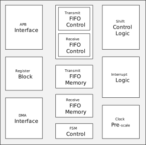
SPI Controller Block Diagram
Bus Interface
APB Interface: The bus interface for control access. The processor reads and writes data, control, and status registers through this interface.
DMA Interface: Generates handshake signals to the central DMA controller, enabling data transfers without CPU intervention. The hardware handshake mechanism prevents data overflow and underflow during high-throughput transfers.
Data Path (Transmit and Receive)
Transmit FIFO Control/Receive FIFO Control: Configures FIFO thresholds and tracks the current fill depth of the transmit and receive paths.
Transmit FIFO Memory/Receive FIFO Memory: Stores data pending transmission or data that has been received.
Shift Control Logic: Serializes data from the transmit FIFO bit by bit onto the SPI bus, and deserializes incoming serial bits into the receive FIFO.
Control and Configuration
Register Block: Contains all configuration registers and serves as the primary software interface for setting operational parameters.
FSM Control: Manages the state transitions of the SPI controller during transmit and receive operations.
Clock and Interrupt
Clock Prescaler: Divides the peripheral clock (pclk) to generate the serial clock (sclk). The sclk frequency can be configured via the BAUDR register.
Interrupt Logic: Generates raw interrupts and interrupt flags that can be individually enabled and cleared by software.