Introduction
The GPIO module is a programmable peripheral that provides flexible control of external I/O pad signals.
The chip integrates multiple independent GPIO controllers, organized as PORT_A, PORT_B, etc. Each port supports the following primary per-pin functions: direction control (input or output), output data control and input state readback via memory-mapped registers, and external interrupt detection for event-driven system response. Within each port, every pin operates independently, allowing fine-grained configuration and monitoring of I/O signals.
Each port contains multiple groups of registers, including basic I/O control registers (GPIO_DR, GPIO_DDR, GPIO_EXT_PORT), interrupt control registers (GPIO_INT_XXX), and debounce control register (GPIO_DB_DIV_CONFIG). The debounce function is controlled at the group level, while all other registers provide bit-level control, with each bit corresponding to an individual GPIO pin.
Features
Up to 64 pins
PortA: PA0 ~ PA31
PortB: PB0 ~ PB31
Up to 52 pins
PortA: PA0 ~ PA31
PortB: PB0 ~ PB19
Up to 52 pins
PortA: PA0 ~ PA31
PortB: PB0 ~ PB19
Up to 52 pins
PortA: PA0 ~ PA31
PortB: PB0 ~ PB19
Up to 52 pins
PortA: PA0 ~ PA31
PortB: PB0 ~ PB19
Up to 96 pins
PortA: PA0 ~ PA31
PortB: PB0 ~ PB31
PortC: PC0 ~ PC31
Up to 94 pins
PortA: PA0 ~ PA31
PortB: PB0 ~ PB31
PortC: PC0 ~ PC29
Output race condition protection
Up to 37 pins
PortA: PA0 ~ PA31
PortB: PB0 ~ PB4
Output race condition protection
Up to 84 pins
AON GPIO: PA0 ~ PA5
SYSON GPIO: PB0 ~ PB4, PF0 ~ PF15, PP0 ~ PP11
CORE GPIO: PC0 ~ PC10, PD0 ~ PD9, PE0 ~ PE16, PS0 ~ PS6
Independent register control
Separate data register and data direction register for each GPIO signal
Flexible interrupt modes
Selectable level-sensitive interrupt detection
Selectable edge-triggered interrupt detection
Debounce capability
Configurable debounce circuitry with slow clock source
Effective noise filtering for interrupt pins
Block Diagram
The block diagram of GPIO is illustrated below.
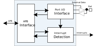
The GPIO block consists of the following main functional interface groups:
APB Interface: Connects to the APB bridge for memory-mapped register access, enabling software configuration and control of GPIO functionality.
External Data Interface: Interfaces directly with physical I/O pads to drive output signals or sample input data from external pins.
Interrupt Interface: Generates interrupt requests to the system interrupt controller when configured GPIO events occur, and receives interrupt acknowledgment signals.