Functional Description
Timer
The timer is primarily used to delay a fixed period after receiving an external stimulus, and then regenerate a stimulus event to the PWM. In the actual circuit, the timer stimulus is not only sent to the PWM but also serves as an input signal for the timer to stop, controlling the timer so that it automatically stops after each timeout overflow.
In practical dimming applications, the timer is often configured at half the mains cycle. For example, under a 50 Hz mains supply, the overflow period of the dimming timer is typically 10 ms.
The following figures show the timer block diagram and the timer timing diagram.
The timer operates as follows:
If the timer detects a high level at the input, the internal counter starts counting up from 0. When a low level is detected, the timer stops operating.
The edg_dtc circuit detects the preceding stimulus signal and triggers the timer to start counting.
If the counter overflows, the of_out overflow signal outputs a high level for one clock cycle. It will be pulled low after one cycle ends.
The edg_dtc circuit detects the of_out pulse signal and triggers the timer to stop counting.
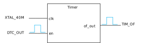
Timer Block Diagram
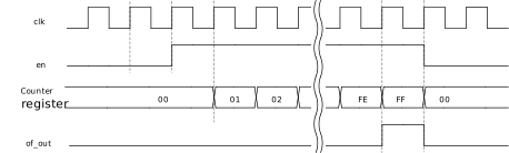
Timer Timing Diagram
In the practical application of UPS, TIM10 is used as the fixed timer.
In the practical application of UPS, TIM10 is used as the fixed timer.
In the practical application of UPS, TIM10 is used as the fixed timer.
In the practical application of UPS, TIM10 is used as the fixed timer.
In the practical application of UPS, TIM10 is used as the fixed timer.
In the practical application of UPS, Basic timer (TIM0~TIM3) is respectively used by PWM timer (TIM4~TIM7) as the fixed timer.
In the practical application of UPS, Basic timer (TIM0~TIM1) is respectively used by PWM timer (TIM4~TIM5) as the fixed timer.
Deglitch Filter and Signal Reverse
To reduce the impact of signal glitches on digital circuits, the deglitch filter uses the XTAL_40MHz sampling clock to debounce the signal. The larger the dbc_cnt value, the wider the glitches that can be filtered, and the longer the delay will be. For different UPS signal sources, adjusting the dbc_cnt value appropriately can filter out glitches while minimizing the delay introduced by digital filtering.
External ZCD signals and CMP outputs can be positive pulse or negative pulse. When the signal is a positive pulse, the system operates normally. When the signal is a negative pulse, configure rvs_en to 1 to reverse the negative pulse signal, ensuring normal system operation.
Edge Detection
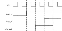
The following figure shows the block diagram of edge detection. The input signals of the edg_dtc module include clk, start_in, and stop_in, and the output is dtc_out.
The edg_dtc module operates as follows:
edg_dtc detects the rising edges of start_in and stop_in.
When a rising edge is detected on start_in, edg_dtc pulls up the dtc_out signal after one clock cycle.
When a rising edge is detected on stop_in, edg_dtc pulls down the dtc_out signal after one clock cycle; otherwise, the dtc_out signal remains high.
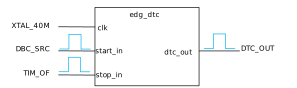
The timing diagram of edge detection is shown in the following figure.
Dimming Signal Types
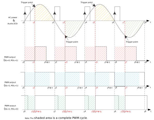
To cooperate with the UPS circuit, the PWM needs to be configured to operate in One Pulse Mode. To meet various demands, parameters such as the default output level of the PWM can be flexibly adjusted during PWM configuration for different control requirements.
OPM_DefaultLevelx = low, CCxPolarity = active_low: Pull down the control signal before the second zero-crossing point.
OPM_DefaultLevelx = high, CCxPolarity = active_low: Pull down the control signal at the second zero-crossing point.
OPM_DefaultLevelx = high, CCxPolarity = active_high: Pull down the control signal after the second zero-crossing point.