串行外设接口 (SPI)
简介
串行外设接口(Serial Peripheral Interface,SPI)是一种用于与外部设备通信的同步串行总线。
芯片实现了 Motorola SPI 协议,作为一种四线同步串行接口,支持全双工、半双工和单工模式。在主机模式下,SPI 控制器提供串行时钟(SCLK),用于与外部从机设备同步数据传输。
特性
支持 Motorola SPI 协议
主机和从机操作模式
两组 SPI 端口
灵活的片选信号 (CS) 管理:
硬件专用片选信号
软件控制片选信号
可编程参数:
SCLK 极性和相位 (SCPOL/SCPH)
串行时钟比特率(主机模式)
RXD 采样延迟周期(主机模式)
4 至 16 位数据帧格式选择
64 个 16 位宽的发送/接收 FIFO
传输模式(主机模式):
发送和接收
仅发送
仅接收
操作模式:
轮询模式
中断模式
DMA 模式
SPI 总线忙碌状态标志
框图
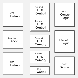
下图展示了 SPI 模块的功能分组。
SPI 控制器框图
总线接口
APB 接口:用于控制访问的总线接口。处理器通过该接口读写数据、控制和状态寄存器。
DMA 接口:向中央 DMA 控制器产生握手信号,无需 CPU 干预即可实现数据传输。硬件握手机制可在高吞吐量传输期间防止数据溢出和下溢。
数据路径(发送与接收)
发送 FIFO 控制 / 接收 FIFO 控制:配置 FIFO 阈值,并跟踪发送和接收路径的当前填充深度。
发送 FIFO 存储器 / 接收 FIFO 存储器:存储等待发送的数据或已接收的数据。
移位控制逻辑:将发送 FIFO 中的数据逐位串行化到 SPI 总线上,并将输入的串行位反序列化到接收 FIFO 中。
控制与配置
寄存器模块:包含所有配置寄存器,作为设置工作参数的主要软件接口。
FSM 控制:管理 SPI 控制器在发送和接收操作期间的状态转换。
时钟与中断
时钟预分频:从外设时钟(pclk)分频得到串行时钟(sclk)。sclk 频率可通过 BAUDR 寄存器进行配置。
中断逻辑:产生原始中断和中断标志,可由软件单独使能和清除。
功能描述
互联拓扑
SPI 可以配置为两种工作模式之一:SPI 主机或 SPI 从机。SPI 可以使用 Motorola 串行外设接口连接任何 SPI 主机或 SPI 从机外设设备。为了通过 SPI 连接到 SPI 主机或 SPI 从机外设设备,该外设必须具备 Motorola 串行外设接口。
SPI 支持的串行协议允许选择 SPI 从机:
单从机:将 SPI 主机的片选引脚连接到 SPI 从机的片选引脚。
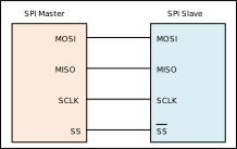
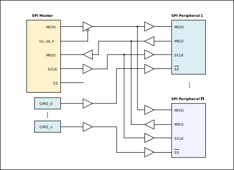
多从机:由于 SPI 主机只有一个片选输出(由 SPI 硬件设计决定),用户应使用 GPIO 来控制多个 SPI 从机。同一时刻只能选择一个从机。
通信格式
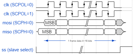
串行时钟相位和时钟极性有四种可能的组合。时钟相位 (SCPH) 决定串行传输是从片选信号的下降沿开始,还是从串行时钟的第一个边沿开始。时钟极性 (SCPOL) 配置参数决定串行时钟的空闲状态是高电平还是低电平。为了正确传输数据,通信双方的 SPI 外设必须具有相同的串行时钟相位 (SCPH) 和时钟极性 (SCPOL) 值。
当配置参数 SCPH = 0 时,数据传输从片选信号的下降沿开始。第一个数据位在串行时钟的第一个边沿被主从外设捕获;因此,在第一个串行时钟边沿到来之前,MOSI 和 MISO 线上必须已经存在有效数据。下图展示了 SCPH = 0 时单次 SPI 数据传输的时序图,分别对应 SCPOL = 0 和 SCPOL = 1 两种配置参数下的串行时钟波形。
SPI 串行格式 (SCPH = 0)
当 SCPH = 0 时,在连续数据传输期间,SPI 主机的片选信号是否在下一个数据帧之前翻转,可以通过 CTRLR0 寄存器中的 SS_T 字段进行配置。无论主机在连续数据传输期间是否翻转片选信号,SPI 从机都能与 SPI 主机正常通信。SS 翻转和 SS 非翻转的时序图如下所示。SS 翻转功能用于兼容不同的 SPI 设备。

SPI 串行格式连续传输 (SCPH = 0,SS 翻转)
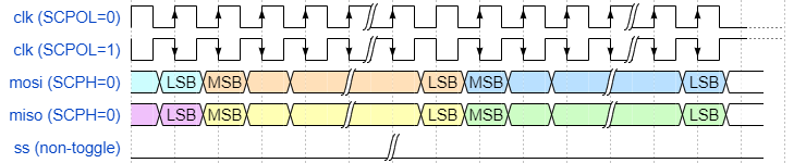
SPI 串行格式连续传输 (SCPH = 0,SS 非翻转)
当配置参数 SCPH = 1 时,主从外设均在片选信号线激活后的第一个串行时钟边沿开始传输数据。第一个数据位在第二个(后沿)串行时钟边沿被捕获。数据由主从外设在串行时钟的前沿上传播。在连续数据帧传输期间,片选信号线可以保持低电平有效状态,直到最后一帧的最后一位被捕获。下图展示了配置参数 SCPH = 1 时 SPI 格式的时序图,分别对应 SCPOL = 0 和 SCPOL = 1 两种配置参数下的串行时钟波形。
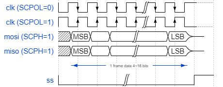
SPI 串行格式 (SCPH = 1)
连续数据帧的传输方式与单帧传输相同,下一帧的最高有效位 (MSB) 紧随当前帧的最低有效位 (LSB) 之后。片选信号在整个传输过程中保持有效。下图展示了配置参数 SCPH = 1 时 SPI 连续传输的时序图。
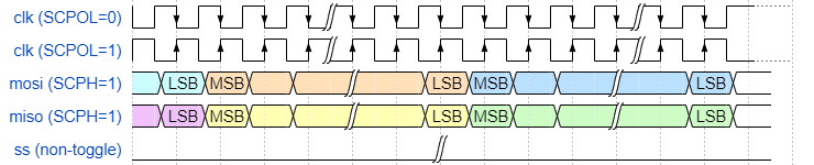
SPI 串行格式连续传输 (SCPH = 1,SS 非翻转)

SPI 串行格式连续传输 (SCPH = 1,SS 翻转)
数据格式
数据帧长度
SPI 控制器支持 4 ~ 16 位可配置的数据帧长度,通过 CTRLR0 寄存器的 DFS 字段设置,复位默认值为 8 位。
无论配置 DFS 为何值,有效数据在 FIFO 中始终右对齐存放,高位自动补零。软件写入数据到寄存器 DR 时,硬件会自动将数据右对齐,发送逻辑仅处理有效位,忽略未使用的高位;接收逻辑则自动将串行输入数据右对齐后存入接收 FIFO,高位补零。
位序交换
SPI 控制器默认以 MSB first(最高有效位优先)的顺序在串行线上传输数据。当需要改为 LSB first(最低有效位优先)时,可通过 CTRLR0 寄存器中的位序交换位对发送或接收通道实现硬件层面的自动交换。交换以 FIFO 条目(16 位)为单位,对高字节 [15:8] 和低字节 [7:0] 各自独立地按位交换,无需软件逐位处理。
发送通道由 TXBITSWAP (CTRLR0[22])控制,接收通道由 RXBITSWAP (CTRLR0[24])控制,两者相互独立,可根据外部设备的要求分别配置。各位置 0 表示不交换(MSB first),置 1 表示交换(LSB first)。
以 DFS = 8 为例,向 DR 写入 0x00B1 (低字节 10110001 ):
配置 |
位序处理 |
输出数据 |
|---|---|---|
TXBITSWAP = 0 |
不交换 (MSB first) |
10110001 (0xB1) |
TXBITSWAP = 1 |
按位交换 (LSB first) |
10001101 (0x8D) |
备注
由于位序交换以完整的 16 位 FIFO 条目为操作对象,建议仅在 DFS = 8 或 DFS = 16 时使能此功能。当 DFS 为其他值时,有效数据位不足 8 或 16 的整数倍,硬件进行高位补零操作,补零位会被卷入交换导致有效数据丢失。
字节序交换
SPI 控制器支持对发送和接收通道分别配置字节序交换,将 FIFO 条目中 16 位数据的高字节 [15:8] 与低字节 [7:0] 互换,默认不交换。当需要修改字节序时,可通过 CTRLR0 寄存器中的字节序交换位实现硬件层面的自动交换,无需软件逐字节处理。
发送通道由 TXBYTESWAP (CTRLR0[21])控制,接收通道由 RXBYTESWAP (CTRLR0[23])控制,两者相互独立,可根据外部设备的要求分别配置。各位置 0 表示不交换(高字节优先),置 1 表示交换(低字节优先)。
以 DFS = 16 为例,向 DR 写入 0xA569 (高字节 0xA5 ,低字节 0x69 ):
配置 |
字节序处理 |
输出数据 |
|---|---|---|
TXBYTESWAP = 0 |
不交换 (高位字节先发) |
0xA5 → 0x69 |
TXBYTESWAP = 1 |
高低字节交换 (低位字节先发) |
0x69 → 0xA5 |
备注
由于字节序交换以完整的 16 位 FIFO 条目为操作对象,建议仅在 DFS = 16 时使能此功能。当 DFS < 16 时,高位区域为补零,字节交换后零字节会被交换到低位,导致有效数据错误。
时钟配置
当 SPI 配置为主机时,串行时钟 (sclk_out) 的最大频率是 SPI 外设时钟 (ssi_clk) 频率的一半。这使得移位控制逻辑能够在 sclk_out 的一个时钟沿捕获数据,并在另一个边沿上传播数据,如下图所示。sclk_out 信号线仅在有效传输进行期间才会翻转。在所有其他时间,它保持非活动状态,由其运行的串行协议所定义。
sclk_out 的频率可由以下公式推导:
Fsclk_out= Fssi_clk/SCKDV
SCKDV 是可编程寄存器 BAUDR 中的一个位字段,取值范围为 0 到 65534 之间的任意偶数值。如果 SCKDV 为 0,则 sclk_out 被禁用。
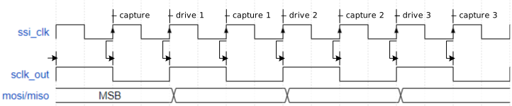
sclk_out/ssi_clk 最大比率
芯片支持高速 SPI 从机。当 SPI 配置为从机时,SPI 主机提供的串行时钟 (sclk_in) 的最大频率可达 ssi_clk 频率的一半。
串行时钟 (sclk_out/sclk_in) 与 SPI 外设时钟 (ssi_clk) 之间的频率比限制总结如下:
主机:Fssi_clk>= 2 x (最大 Fsclk_out)
从机:Fssi_clk>= 2 x (最大 Fsclk_in)
SPI0 和 SPI1 的 Fssi_clk相同,最高可支持 100 MHz。
备注
Fssi_clk受 Bootloader 阶段的 PLL(锁相环)配置影响。
传输模式
在串行总线上传输数据时,SPI 主机可以工作在多种工作模式,具体如下。传输模式(TMOD)通过写入控制寄存器 0(CTRLR0)来设置。
在串行总线上传输数据时,SPI 从机硬件固定工作在全双工模式。也就是说,CTRLR0 寄存器中的 TMOD 字段对 SPI 从机无效,因为从机硬件始终同时进行发送和接收操作。如果不希望该设备返回数据,可以通过 CTRLR0 中的 SLV_OE 位禁用从机输出。
全双工模式
当 TMOD = 2'b00 时,发送和接收逻辑均有效。发送数据从发送 FIFO 中弹出,通过 MOSI 线发送至目标设备,目标设备通过 MISO 线返回数据。来自目标设备的接收数据在每个数据帧结束时,从接收移位寄存器移入接收 FIFO。
半双工-仅发送模式
当 TMOD = 2'b01 时,接收数据无效,不应存入接收 FIFO。发送数据从发送 FIFO 中弹出,通过 MOSI 线发送至目标设备,目标设备通过 MISO 线返回数据。在数据帧结束时,接收移位寄存器不会将新接收的数据加载到接收 FIFO 中。接收移位寄存器中的数据将在下一次传输时被覆盖。进入该模式时,应屏蔽来自接收逻辑的中断。
半双工-仅接收模式
当 TMOD = 2'b10 时,发送数据无效。传输期间 MOSI 输出保持恒定的逻辑电平。来自目标设备的接收数据在每个数据帧结束时,从接收移位寄存器移入接收 FIFO。进入该模式时,应屏蔽来自发送逻辑的中断。
FIFO 管理
发送和接收 FIFO 缓冲区的深度均为 64。由于串行规范规定一次串行传输(数据帧)的长度为 4 到 16 位,因此宽度固定为 16 位。FIFO 中的每个数据条目包含一个数据帧。
备注
当 SPI 被禁用(SSI_EN = 0)或复位时,发送和接收 FIFO 将被清空。
发送 FIFO 通过对 SPI 数据寄存器(DR)的 APB 写操作进行加载。数据由移位控制逻辑从发送 FIFO 中弹出(移除)到发送移位寄存器。当 FIFO 中的条目数小于或等于 FIFO 阈值时,发送 FIFO 会产生 FIFO 空中断请求(ssi_txe_intr)。该阈值通过可编程寄存器 TXFTLR 设置,用于确定产生中断时的 FIFO 条目级别。该阈值可以为处理器提供发送 FIFO 即将为空的早期指示。如果尝试向已满的发送 FIFO 写入数据,将产生发送 FIFO 溢出中断(ssi_txo_intr)。
数据通过对 SPI 数据寄存器(DR)的 APB 读操作从接收 FIFO 中弹出。接收 FIFO 由接收移位寄存器通过移位控制逻辑进行加载。当 FIFO 中的条目数大于或等于 FIFO 阈值加 1 时,接收 FIFO 会产生 FIFO 满中断请求(ssi_rxf_intr)。该阈值通过可编程寄存器 RXFTLR 设置,用于确定产生中断时的 FIFO 条目级别。
该阈值可以为处理器提供接收 FIFO 即将满的早期指示。当接收移位逻辑尝试向已满的接收 FIFO 加载数据时,将产生接收 FIFO 溢出中断(ssi_rxo_intr),而且新接收的数据将会丢失。如果尝试从空的接收 FIFO 读取数据,将产生接收 FIFO 下溢中断(ssi_rxu_intr)。这会提醒处理器读取的数据无效。
中断处理
SPI 支持组合中断请求和独立中断请求,每种中断都可以被屏蔽。组合中断请求是所有其他 SPI 中断经过屏蔽后的或(OR)运算结果。系统设计者可以选择将独立中断请求或仅将组合中断请求路由到中断控制器。
中断描述
各中断的触发条件和清除方式描述如下:
发送 FIFO 空中断(
ssi_txe_intr)——当发送 FIFO 等于或低于其阈值时置位,需要服务以防止下溢。该阈值通过软件可编程寄存器设置,用于确定产生中断时的发送 FIFO 条目级别。当数据写入发送 FIFO 并使其超过阈值级别时,该中断由硬件自动清除。发送 FIFO 溢出中断(
ssi_txo_intr)——当 APB 访问尝试向已满的发送 FIFO 写入数据时置位。置位时,来自 APB 的写入数据将被丢弃。该中断保持置位状态,直到读取发送 FIFO 溢出中断清除寄存器(TXOICR)。接收 FIFO 下溢中断(
ssi_rxu_intr)——当 APB 访问尝试从空的接收 FIFO 读取数据时置位。置位时,从接收 FIFO 读回的数据为零。该中断保持置位状态,直到读取接收 FIFO 下溢中断清除寄存器(RXUICR)。接收 FIFO 溢出中断(
ssi_rxo_intr)——当接收逻辑尝试在接收 FIFO 已满时放入数据时置位。置位时,新接收的数据将被丢弃。该中断保持置位状态,直到读取接收 FIFO 溢出中断清除寄存器(RXOICR)。接收 FIFO 满中断(
ssi_rxf_intr)——当接收 FIFO 等于或高于其阈值加 1 时置位,需要服务以防止溢出。该阈值通过软件可编程寄存器设置,用于确定产生中断时的接收 FIFO 条目级别。当数据从接收 FIFO 中读取并使其降至阈值级别以下时,该中断由硬件自动清除。帧对齐错误中断(
ssi_fae_intr)——仅当 SPI 被配置为 SPI 从机设备时有效。当接收到的数据帧长度与 CTRLR0 中的 DFS (数据帧大小)设置不匹配时,该中断置位。该中断保持置位状态,直到读取帧对齐错误中断清除寄存器( MSTICR_FAEICR )。多主机冲突中断(
ssi_mst_intr)——暂不支持。发送 FIFO 下溢中断(
ssi_txu_intr)——仅当 SPI 被配置为 SPI 从机设备时有效。当发送逻辑尝试从空的发送 FIFO 读取数据时,该中断置位。置位时,从机设备发送的数据无效。该中断保持置位状态,直到读取发送 FIFO 下溢中断清除寄存器(TXUICR)。SS_N 上升沿检测中断(
ssi_ssr_intr)——仅当 SPI 被配置为 SPI 从机设备时有效。当检测到 SS_N 上升沿时,该中断置位。该中断保持置位状态,直到读取 SS_N 上升沿检测中断清除寄存器(SSRICR)。
中断屏蔽
SPI 中断屏蔽寄存器(SPI_IMR)用于控制各中断源是否被屏蔽。每个屏蔽位对应一个中断源,置 1 表示不屏蔽(使能中断),置 0 表示屏蔽(禁用中断)。各屏蔽位定义如下:
发送 FIFO 空中断屏蔽(SPI_BIT_TXEIM)——用于控制
ssi_txe_intr中断。发送 FIFO 溢出中断屏蔽(SPI_BIT_TXOIM)——用于控制
ssi_txo_intr中断。接收 FIFO 下溢中断屏蔽(SPI_BIT_RXUIM)——用于控制
ssi_rxu_intr中断。接收 FIFO 溢出中断屏蔽(SPI_BIT_RXOIM)——用于控制
ssi_rxo_intr中断。接收 FIFO 满中断屏蔽(SPI_BIT_RXFIM)——用于控制
ssi_rxf_intr中断。多主机冲突/帧对齐错误中断屏蔽(SPI_BIT_MSTIM_FAEIM)——当 SPI 配置为主机时,用于控制
ssi_mst_intr中断;当 SPI 配置为从机时,用于控制ssi_fae_intr中断。发送 FIFO 下溢中断屏蔽(SPI_BIT_TXUIM)——仅当 SPI 配置为从机时有效,用于控制
ssi_txu_intr中断。SS_N 上升沿检测中断屏蔽(SPI_BIT_SSRIM)——仅当 SPI 配置为从机时有效,用于控制
ssi_ssr_intr中断。
模式选择
芯片作为 SPI 主机或 SPI 从机工作时使用两组不同的电路,因此用户必须在初始化设备之前设置 SPI 角色,相关寄存器描述如下。
REG_LSYSPLAT_CTRL
Size: 32
Address: 0x41008230
Read/write access: R/W
Bit |
Symbol |
Access |
INI |
Description |
|---|---|---|---|---|
27 |
SPI1_MST |
R/W |
0h |
|
26 |
SPI0_MST |
R/W |
0h |
|
REG_LSYSPLAT_CTRL
Size: 32
Address: 0x4100C230
Read/write access: R/W
Bit |
Symbol |
Access |
INI |
Description |
|---|---|---|---|---|
27 |
SPI1_MST |
R/W |
0h |
|
26 |
SPI0_MST |
R/W |
0h |
|
REG_LSYSPLAT_CTRL
Size: 32
Address: 0x4100C230
Read/write access: R/W
Bit |
Symbol |
Access |
INI |
Description |
|---|---|---|---|---|
27 |
SPI1_MST |
R/W |
0h |
|
26 |
SPI0_MST |
R/W |
0h |
|
REG_LSYSPLAT_CTRL
Size: 32
Address: 0x4100C230
Read/write access: R/W
Bit |
Symbol |
Access |
INI |
Description |
|---|---|---|---|---|
27 |
SPI1_MST |
R/W |
0h |
|
26 |
SPI0_MST |
R/W |
0h |
|
REG_LSYSPLAT_CTRL
Size: 32
Address: 0x4100C230
Read/write access: R/W
Bit |
Symbol |
Access |
INI |
Description |
|---|---|---|---|---|
27 |
SPI1_MST |
R/W |
0h |
|
26 |
SPI0_MST |
R/W |
0h |
|
REG_HSYSHPLAT_CTRL
Size: 32
Address: 0x41000030
Read/write access: R/W
Bit |
Symbol |
Access |
INI |
Description |
|---|---|---|---|---|
26 |
SPI1_MST |
R/W |
0h |
|
25 |
SPI0_MST |
R/W |
0h |
|
REG_LSYSPLAT_CTRL
Size: 32
Address: 0x4080A2A0
Read/write access: R/W
Bit |
Symbol |
Access |
INI |
Description |
|---|---|---|---|---|
27 |
SPI1_MST |
R/W |
0h |
|
26 |
SPI0_MST |
R/W |
0h |
|
REG_LSYSPLAT_CTRL
Size: 32
Address: 0x408012A0
Read/write access: R/W
Bit |
Symbol |
Access |
INI |
Description |
|---|---|---|---|---|
27 |
SPI1_MST |
R/W |
0h |
|
26 |
SPI0_MST |
R/W |
0h |
|
主机模式
该模式实现与 SPI 从机外设的串行通信。当配置为 SPI 主机时,SPI 发起并控制所有串行传输。此 图示 展示了 SPI 配置为 SPI 主机的示例,串行总线上所有其他设备通过 GPIO 进行片选控制。
由 SPI 主机生成并控制的串行时钟通过 sclk_out 线输出。当 SPI 被禁用(SSI_EN = 0)时,不会发生串行传输, sclk_out 保持非活动状态。
传输控制
数据传输由 SPI 主机发起和控制,涉及启动、停止和状态三部分。
启动
传输开始前需拉低片选信号:若使用模块自带的片选信号(硬件 CS),该信号由硬件自动拉低;若使用 GPIO 模拟片选信号(软件 CS),则需要用户手动控制 GPIO 将其拉低。
传输启动需满足三个条件:SPI 被使能(SSI_EN=1)、发送 FIFO 中至少存在一个有效数据条目、且一个 SPI 从机被选中。为确保连续传输的完整性,也可在使能从机之前,预先向发送 FIFO 写入至少两个数据条目,使传输在 FIFO 中积累足够数据帧后才真正开始。
对于仅接收模式(TMOD = 2'b10),启动方式略有不同:需在选择从机时向发送 FIFO 写入哑数据(dummy data)以触发串行时钟。传输期间 MOSI 输出保持恒定逻辑电平,发送 FIFO 仅在起始时弹出一次,之后可保持为空。
发送 FIFO 阈值(TXFTLR)可在 FIFO 条目数降至阈值以下时产生提前中断(ssi_txe_intr),通知处理器发送 FIFO 即将为空。使用 DMA 时,发送数据级别(DMATDLR)可向 DMA 控制器发出提前请求(dma_tx_req),以便及时补充数据、维持连续传输。
接收 FIFO 阈值(RXFTLR)可在 FIFO 条目数达到阈值加 1 时给出即将满的提前指示。使用 DMA 时,接收数据级别(DMARDLR)可向 DMA 控制器发出提前请求(dma_rx_req),以便及时读取数据、防止溢出。
停止
不同传输模式下的停止条件如下:
在双工(收发)模式和单工仅发送模式(TMOD = 2'b00 或 TMOD = 2'b01)下,发送 FIFO 为空时移位控制逻辑终止传输。因此进行连续数据传输时,需确保所有数据传输完毕之前发送 FIFO 不会变空。
在单工仅接收模式(TMOD = 2'b10)下,传输结束由控制寄存器 1(CTRLR1)中的数据帧数量(NDF)字段决定。当接收帧数等于 NDF + 1 时,接收逻辑终止传输。例如需接收 24 帧,应将 NDF 编程为 23。该模式下发送 FIFO 无需在传输期间持续服务,可节省 APB 带宽,但应在每次接收 FIFO 产生满中断时及时读取数据以防止溢出。
传输完成后需拉高片选信号:若使用硬件 CS,该信号由硬件自动拉高;若使用软件 CS,则需要用户手动控制 GPIO 将其拉高。
状态
在 SPI 传输过程中,状态寄存器(SPI_SR)中的忙标志(BUSY)用于指示当前传输状态:
置位(1):表示 SPI 正在进行数据传输
清除(0):表示 SPI 处于空闲状态
在发起下一次串行传输之前,必须先检查并等待 BUSY 标志清除。
片选控制
不支持。
不支持。
不支持。
不支持。
不支持。
不支持。
在某些场景下,中断可能无法及时响应以填充 TX FIFO,从而导致其出现空闲状态。因此,寄存器 CTRLR0 中的 CSF_EN 位允许 SPI 主机强制将片选信号保持为低电平,直到整个传输过程完成。此外,在尚未完成的传输过程中,当 TX FIFO 为空时,SPI 主机会保持 CS 信号为低电平并暂停传输(不发送 sclk 时钟信号)。
当 CSF_EN 位使能时,SPI 主机会计算待发送的数据比特数。计算方式为数据帧大小(CTRLR0 [3:0])乘以数据帧数量(CTRLR1 [15:0])。随后,SPI 主机在传输期间强制将片选信号保持为低电平。仅当已发送的数据比特数达到计算值时,SPI 主机才会释放该强制控制。CSF_EN 的使用示例如下所示。
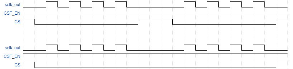
在某些场景下,中断可能无法及时响应以填充 TX FIFO,从而导致其出现空闲状态。因此,寄存器 CTRLR0 中的 CSF_EN 位允许 SPI 主机强制将片选信号保持为低电平,直到整个传输过程完成。此外,在尚未完成的传输过程中,当 TX FIFO 为空时,SPI 主机会保持 CS 信号为低电平并暂停传输(不发送 sclk 时钟信号)。
当 CSF_EN 位使能时,SPI 主机会计算待发送的数据比特数。计算方式为数据帧大小(CTRLR0 [3:0])乘以数据帧数量(CTRLR1 [15:0])。随后,SPI 主机在传输期间强制将片选信号保持为低电平。仅当已发送的数据比特数达到计算值时,SPI 主机才会释放该强制控制。CSF_EN 的使用示例如下所示。
接收延迟采样
从机使用来自主机的时钟信号作为选通信号,将数据驱动到 MISO 线上。由于时钟信号存在往返路由延迟,从机的数据输出在主机看来可能会延迟到达,从而偏离正常的采样时间。当 SPI 配置为主机时,可以包含额外的逻辑来延迟 MISO 信号的默认采样时间,这有助于提高串行总线上的最大可实现频率。
下图展示了 MOSI 信号上的路由延迟如何导致主机在默认采样时刻采样到错误 MISO 值的示例。蓝色箭头表示主机和从机之间的路由延迟;红色线表示从机从接收时钟到在 MISO 线上驱动数据输出的采样延迟。
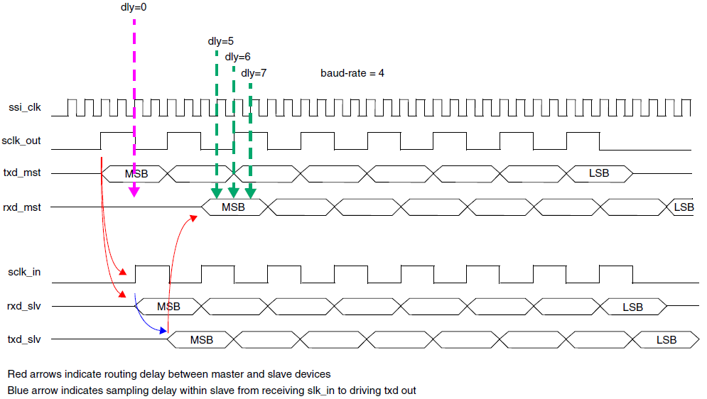
时钟信号往返路由延迟的影响
当包含 RXD 采样延迟逻辑时,可以动态编程延迟值,将 rxd 信号的采样时间从默认值偏移若干个 pclk 周期。
采样延迟逻辑的分辨率为一个 pclk 周期。软件可以通过编写一个持续从从机读取并递增主机 RXD 采样延迟值的循环来"校准"串行总线,直到主机接收到正确的数据。
备注
用于延迟 rxd 输入采样的最大 ssi_clk 周期数为 4。如果编程的延迟值超过此最大值,将对 rxd 采样应用零(0)延迟。
从机模式
该模式实现与 SPI 主机外设的串行通信。当 SPI 配置为从机设备时,所有串行传输均由串行总线主机发起并控制。
SPI 从机只能在发送和接收模式下工作。也就是说,CTRLR0 寄存器中的 TMOD 字段对 SPI 从机无效。如果不希望该设备响应数据,可以通过 CTRLR0 中的 SLV_OE 位禁用从机输出。
当在配置期间选择 SPI 从机时,它会将 MISO 数据输出到串行总线上。进出 SPI 从机的所有数据传输都由串行时钟线(sclk_in)控制,该时钟线由 SPI 主机驱动。数据在串行时钟线的一个边沿上从 SPI 从机传播,并在相对的边沿上进行采样。
当 SPI 从机未被选中时,不得干扰 SPI 主机与其他 SPI 从机设备之间的数据传输。当 SPI 从机未被选中时,其 MISO 输出被缓冲,在 SPI 主机的 MISO 线上呈现高阻抗驱动。
调节数据传输的串行时钟由 SPI 主机产生,并通过 sclk_in 输入到 SPI 从机。从机保持空闲状态,直到被总线主机选中。当不主动传输数据时,从机必须将其 MISO 线保持在高阻抗状态,以避免干扰到其他从机设备的串行传输。只要从机被选中,它就会继续与主机之间进行数据传输。
传输控制
如果 SPI 从机要向主机传输数据,必须确保在 SPI 主机发起传输之前发送 FIFO 中已存在数据。如果主机在发送 FIFO 中没有数据的情况下向 SPI 从机发起传输,则 SPI 状态寄存器中会设置错误标志(TXE),并且之前传输的数据帧会在 MISO 上重新发送。对于连续数据传输,必须确保在所有数据传输完成之前发送 FIFO 不会变空。发送 FIFO 阈值级别寄存器(TXFTLR)可用于向处理器生成提前中断(ssi_txe_intr),指示发送 FIFO 即将变空。当使用 DMA 控制器进行 APB 访问时,DMA 发送数据级别寄存器(DMATDLR)可用于向 DMA 控制器生成提前请求(dma_tx_req),指示发送 FIFO 即将变空。随后可以用数据重新填充 FIFO 以继续串行传输。
每次接收 FIFO 产生 FIFO 满中断请求时,都应读取接收 FIFO,以防止溢出。接收 FIFO 阈值级别寄存器(RXFTLR)可用于提前指示接收 FIFO 即将满。当使用 DMA 控制器进行 APB 访问时,DMA 接收数据级别寄存器(DMARDLR)可用于向 DMA 控制器生成提前请求(dma_rx_req),指示接收 FIFO 即将满。
DMA 支持
SPI 具有可选的内置 DMA 功能,可在配置时选择;它具有与 DMA 控制器的握手接口,用于请求和控制传输。APB 总线用于执行与 DMA 之间的数据传输。
SPI 使用两个 DMA 通道,一个用于发送数据,一个用于接收数据。SPI 具有以下 DMA 寄存器:
DMACR:控制寄存器,用于启用 DMA 操作。
DMATDLR:发送阈值寄存器,用于设置触发 DMA 请求的发送 FIFO 数据量阈值。
DMARDLR:接收阈值寄存器,用于设置触发 DMA 请求的接收 FIFO 数据量阈值。
要在 SPI 上启用 DMA 控制器接口,必须写入 DMA 控制寄存器(DMACR)。在 DMACR 的 TDMAE 位字段中写入 '1' 可启用 SPI 发送握手接口。在 DMACR 的 RDMAE 位字段中写入 '1' 可启用 SPI 接收握手接口。
发送数据阈值与发送 FIFO 下溢
在 SPI 串行传输期间,每当发送 FIFO 中的数据条目数小于或等于 DMA 发送数据级别寄存器(DMATDLR)的值时,就会向 DMA 控制器发起发送 FIFO 请求,该值称为发送数据阈值。DMA 控制器通过向发送 FIFO 写入一批突发数据作为响应。
应足够频繁地从 DMA 获取数据,以确保发送 FIFO 能够持续进行串行传输;也就是说,当 FIFO 快要变空时,应及时触发另一次 DMA 请求。否则,FIFO 将发生数据耗尽(下溢)。为防止此情况,用户必须正确设置阈值。
接收数据阈值与接收 FIFO 溢出
在 SPI 串行传输期间,每当接收 FIFO 中的数据条目数达到或超过 DMA 接收数据级别寄存器的值时,即 DMARDLR+1,就会向 DMA 控制器发起接收 FIFO 请求,该值称为接收数据阈值。DMA 控制器通过从接收 FIFO 获取一批突发数据作为响应。
DMA 应足够频繁地获取数据,以确保接收 FIFO 能够持续接收串行传输的数据;也就是说,当 FIFO 快要填满时,应及时请求另一次 DMA 传输。否则,FIFO 将发生数据溢出。为防止此情况,用户必须正确设置阈值。
寄存器
本节描述了 SPI 的可编程寄存器。下表提供了 SPI 内存映射的详细信息。SPI 中的所有寄存器均以 32 位边界寻址,以保持与 AHB 总线的一致性。当任何寄存器的物理宽度小于 32 位时,32 位边界中未使用的高位为保留位。对这些保留位进行写操作无效;读取这些位返回 0。
Base Address:
SPI0_REG : 0x40124000
SPI1_REG : 0x40125000
Name |
Address offset |
Access |
Description |
|---|---|---|---|
000h |
R/W |
This register controls the serial data transfer. It is impossible to write to this register when the SPI is enabled. The SPI is enabled and disabled by writing to the SSIENR register. |
|
004h |
R/W |
This register exists only when the SPI is configured as a master device. When the SPI is configured as a serial slave, writing to this location has no effect; reading from this location returns 0. Control register 1 controls the end of serial transfers when in receive-only mode. It is impossible to write to this register when the SPI is enabled. The SPI is enabled and disabled by writing to the SSIENR register. |
|
008h |
R/W |
This register enables and disables the SPI. |
|
010h |
R/W |
This register is valid only when the SPI is configured as a master device. When the SPI is configured as a serial slave, writing to this location has no effect; reading from this location returns 0. You cannot write to this register when SPI is busy. |
|
014h |
R/W |
This register is valid only when the SPI is configured as a master device. When the SPI is configured as a serial slave, writing to this location has no effect; reading from this location returns 0. The register derives the frequency of the serial clock that regulates the data transfer. The 16-bit field in this register defines the ssi_clk divider value. It is impossible to write to this register when the SPI is enabled. The SPI is enabled and disabled by writing to the SSIENR register. |
|
018h |
R/W |
This register controls the threshold value for the transmit FIFO memory. It is impossible to write to this register when the SPI is enabled. The SPI is enabled and disabled by writing to the SSIENR register. |
|
01Ch |
R/W |
This register controls the threshold value for the receive FIFO memory. It is impossible to write to this register when the SPI is enabled. The SPI is enabled and disabled by writing to the SSIENR register. |
|
020h |
R |
This register contains the number of valid data entries in the transmit FIFO memory. |
|
024h |
R |
This register contains the number of valid data entries in the receive FIFO memory. This register can be read at any time. |
|
028h |
R |
This is a read-only register used to indicate the current transfer status, FIFO status, and any transmission/reception errors that may have occurred. The status register may be read at any time. None of the bits in this register request an interrupt. |
|
02Ch |
R/W |
This read/write register masks or enables all interrupts generated by the SPI. |
|
030h |
R |
This register reports the status of the SPI interrupts after they have been masked. |
|
034h |
R |
This read-only register reports the status of the SPI interrupts prior to masking. |
|
038h |
R |
||
03Ch |
R |
||
040h |
R |
||
044h |
R |
Serial-master : MSTICR is not used because ss_in_n is tie 1 for Motorola-SPI, ssi_mst_intr is not used. |
|
048h |
R |
||
04Ch |
R/W |
This register is only valid when SPI is configured with a set of DMA Controller interface signals. |
|
050h |
R/W |
This register is only valid when the SPI is configured with a set of DMA interface signals. |
|
054h |
R/W |
This register is only valid when SPI is configured with a set of DMA interface signals. |
|
058h |
R |
This register is present only if SPI is configured as serial-slave. |
|
05Ch |
R |
This register is present only if SPI is configured as serial-slave. |
|
060h |
R/W |
The SPI data register is a 16-bit read/write buffer for the transmit/receive FIFOs. When the register is read, data in the receive FIFO buffer is accessed. When it is written to, data are moved into the transmit FIFO buffer; a write can occur only when SSI_EN = 1. FIFOs are reset when SSI_EN = 0. Note1: If the Data Register (DR) is accessed from an AHB master (such as a DMA controller or a processor), the AHB transfer type may be a burst. During AHB burst transfers, the address increments after each beat of the burst. To facilitate an AHB burst, read, or write operation to the transmit or receive FIFO, the Date Register occupies thirty-six 32-bit address locations of memory map. Each of the 16-bit address locations are aliased to the DR; single accesses to the DR may use any of the 16-bit address locations. Note2: The DR register in the SPI occupies thirty-six 32-bit address locations of the memory map to facilitate AHB burst transfers. Writing to any of these address locations has the same effect as pushing the data from the pwdata bus into the transmit FIFO. Reading from any of these locations has the same effect as popping data from the receive FIFO onto the prdata bus. The FIFO buffers on the SPI are not addressable. |
|
064h |
R/W |
The SPI data register is a 16-bit read/write buffer for the transmit/receive FIFOs. When the register is read, data in the receive FIFO buffer is accessed. When it is written to, data are moved into the transmit FIFO buffer; a write can occur only when SSI_EN = 1. FIFOs are reset when SSI_EN = 0. Note1: If the Data Register (DR) is accessed from an AHB master (such as a DMA controller or a processor), the AHB transfer type may be a burst. During AHB burst transfers, the address increments after each beat of the burst. To facilitate an AHB burst, read, or write operation to the transmit or receive FIFO, the Date Register occupies thirty-six 32-bit address locations of memory map. Each of the 16-bit address locations are aliased to the DR; single accesses to the DR may use any of the 16-bit address locations. Note2: The DR register in the SPI occupies thirty-six 32-bit address locations of the memory map to facilitate AHB burst transfers. Writing to any of these address locations has the same effect as pushing the data from the pwdata bus into the transmit FIFO. Reading from any of these locations has the same effect as popping data from the receive FIFO onto the prdata bus. The FIFO buffers on the SPI are not addressable. |
|
068h |
R/W |
The SPI data register is a 16-bit read/write buffer for the transmit/receive FIFOs. When the register is read, data in the receive FIFO buffer is accessed. When it is written to, data are moved into the transmit FIFO buffer; a write can occur only when SSI_EN = 1. FIFOs are reset when SSI_EN = 0. Note1: If the Data Register (DR) is accessed from an AHB master (such as a DMA controller or a processor), the AHB transfer type may be a burst. During AHB burst transfers, the address increments after each beat of the burst. To facilitate an AHB burst, read, or write operation to the transmit or receive FIFO, the Date Register occupies thirty-six 32-bit address locations of memory map. Each of the 16-bit address locations are aliased to the DR; single accesses to the DR may use any of the 16-bit address locations. Note2: The DR register in the SPI occupies thirty-six 32-bit address locations of the memory map to facilitate AHB burst transfers. Writing to any of these address locations has the same effect as pushing the data from the pwdata bus into the transmit FIFO. Reading from any of these locations has the same effect as popping data from the receive FIFO onto the prdata bus. The FIFO buffers on the SPI are not addressable. |
|
06Ch |
R/W |
The SPI data register is a 16-bit read/write buffer for the transmit/receive FIFOs. When the register is read, data in the receive FIFO buffer is accessed. When it is written to, data are moved into the transmit FIFO buffer; a write can occur only when SSI_EN = 1. FIFOs are reset when SSI_EN = 0. Note1: If the Data Register (DR) is accessed from an AHB master (such as a DMA controller or a processor), the AHB transfer type may be a burst. During AHB burst transfers, the address increments after each beat of the burst. To facilitate an AHB burst, read, or write operation to the transmit or receive FIFO, the Date Register occupies thirty-six 32-bit address locations of memory map. Each of the 16-bit address locations are aliased to the DR; single accesses to the DR may use any of the 16-bit address locations. Note2: The DR register in the SPI occupies thirty-six 32-bit address locations of the memory map to facilitate AHB burst transfers. Writing to any of these address locations has the same effect as pushing the data from the pwdata bus into the transmit FIFO. Reading from any of these locations has the same effect as popping data from the receive FIFO onto the prdata bus. The FIFO buffers on the SPI are not addressable. |
|
070h |
R/W |
The SPI data register is a 16-bit read/write buffer for the transmit/receive FIFOs. When the register is read, data in the receive FIFO buffer is accessed. When it is written to, data are moved into the transmit FIFO buffer; a write can occur only when SSI_EN = 1. FIFOs are reset when SSI_EN = 0. Note1: If the Data Register (DR) is accessed from an AHB master (such as a DMA controller or a processor), the AHB transfer type may be a burst. During AHB burst transfers, the address increments after each beat of the burst. To facilitate an AHB burst, read, or write operation to the transmit or receive FIFO, the Date Register occupies thirty-six 32-bit address locations of memory map. Each of the 16-bit address locations are aliased to the DR; single accesses to the DR may use any of the 16-bit address locations. Note2: The DR register in the SPI occupies thirty-six 32-bit address locations of the memory map to facilitate AHB burst transfers. Writing to any of these address locations has the same effect as pushing the data from the pwdata bus into the transmit FIFO. Reading from any of these locations has the same effect as popping data from the receive FIFO onto the prdata bus. The FIFO buffers on the SPI are not addressable. |
|
074h |
R/W |
The SPI data register is a 16-bit read/write buffer for the transmit/receive FIFOs. When the register is read, data in the receive FIFO buffer is accessed. When it is written to, data are moved into the transmit FIFO buffer; a write can occur only when SSI_EN = 1. FIFOs are reset when SSI_EN = 0. Note1: If the Data Register (DR) is accessed from an AHB master (such as a DMA controller or a processor), the AHB transfer type may be a burst. During AHB burst transfers, the address increments after each beat of the burst. To facilitate an AHB burst, read, or write operation to the transmit or receive FIFO, the Date Register occupies thirty-six 32-bit address locations of memory map. Each of the 16-bit address locations are aliased to the DR; single accesses to the DR may use any of the 16-bit address locations. Note2: The DR register in the SPI occupies thirty-six 32-bit address locations of the memory map to facilitate AHB burst transfers. Writing to any of these address locations has the same effect as pushing the data from the pwdata bus into the transmit FIFO. Reading from any of these locations has the same effect as popping data from the receive FIFO onto the prdata bus. The FIFO buffers on the SPI are not addressable. |
|
078h |
R/W |
The SPI data register is a 16-bit read/write buffer for the transmit/receive FIFOs. When the register is read, data in the receive FIFO buffer is accessed. When it is written to, data are moved into the transmit FIFO buffer; a write can occur only when SSI_EN = 1. FIFOs are reset when SSI_EN = 0. Note1: If the Data Register (DR) is accessed from an AHB master (such as a DMA controller or a processor), the AHB transfer type may be a burst. During AHB burst transfers, the address increments after each beat of the burst. To facilitate an AHB burst, read, or write operation to the transmit or receive FIFO, the Date Register occupies thirty-six 32-bit address locations of memory map. Each of the 16-bit address locations are aliased to the DR; single accesses to the DR may use any of the 16-bit address locations. Note2: The DR register in the SPI occupies thirty-six 32-bit address locations of the memory map to facilitate AHB burst transfers. Writing to any of these address locations has the same effect as pushing the data from the pwdata bus into the transmit FIFO. Reading from any of these locations has the same effect as popping data from the receive FIFO onto the prdata bus. The FIFO buffers on the SPI are not addressable. |
|
07Ch |
R/W |
The SPI data register is a 16-bit read/write buffer for the transmit/receive FIFOs. When the register is read, data in the receive FIFO buffer is accessed. When it is written to, data are moved into the transmit FIFO buffer; a write can occur only when SSI_EN = 1. FIFOs are reset when SSI_EN = 0. Note1: If the Data Register (DR) is accessed from an AHB master (such as a DMA controller or a processor), the AHB transfer type may be a burst. During AHB burst transfers, the address increments after each beat of the burst. To facilitate an AHB burst, read, or write operation to the transmit or receive FIFO, the Date Register occupies thirty-six 32-bit address locations of memory map. Each of the 16-bit address locations are aliased to the DR; single accesses to the DR may use any of the 16-bit address locations. Note2: The DR register in the SPI occupies thirty-six 32-bit address locations of the memory map to facilitate AHB burst transfers. Writing to any of these address locations has the same effect as pushing the data from the pwdata bus into the transmit FIFO. Reading from any of these locations has the same effect as popping data from the receive FIFO onto the prdata bus. The FIFO buffers on the SPI are not addressable. |
|
080h |
R/W |
The SPI data register is a 16-bit read/write buffer for the transmit/receive FIFOs. When the register is read, data in the receive FIFO buffer is accessed. When it is written to, data are moved into the transmit FIFO buffer; a write can occur only when SSI_EN = 1. FIFOs are reset when SSI_EN = 0. Note1: If the Data Register (DR) is accessed from an AHB master (such as a DMA controller or a processor), the AHB transfer type may be a burst. During AHB burst transfers, the address increments after each beat of the burst. To facilitate an AHB burst, read, or write operation to the transmit or receive FIFO, the Date Register occupies thirty-six 32-bit address locations of memory map. Each of the 16-bit address locations are aliased to the DR; single accesses to the DR may use any of the 16-bit address locations. Note2: The DR register in the SPI occupies thirty-six 32-bit address locations of the memory map to facilitate AHB burst transfers. Writing to any of these address locations has the same effect as pushing the data from the pwdata bus into the transmit FIFO. Reading from any of these locations has the same effect as popping data from the receive FIFO onto the prdata bus. The FIFO buffers on the SPI are not addressable. |
|
084h |
R/W |
The SPI data register is a 16-bit read/write buffer for the transmit/receive FIFOs. When the register is read, data in the receive FIFO buffer is accessed. When it is written to, data are moved into the transmit FIFO buffer; a write can occur only when SSI_EN = 1. FIFOs are reset when SSI_EN = 0. Note1: If the Data Register (DR) is accessed from an AHB master (such as a DMA controller or a processor), the AHB transfer type may be a burst. During AHB burst transfers, the address increments after each beat of the burst. To facilitate an AHB burst, read, or write operation to the transmit or receive FIFO, the Date Register occupies thirty-six 32-bit address locations of memory map. Each of the 16-bit address locations are aliased to the DR; single accesses to the DR may use any of the 16-bit address locations. Note2: The DR register in the SPI occupies thirty-six 32-bit address locations of the memory map to facilitate AHB burst transfers. Writing to any of these address locations has the same effect as pushing the data from the pwdata bus into the transmit FIFO. Reading from any of these locations has the same effect as popping data from the receive FIFO onto the prdata bus. The FIFO buffers on the SPI are not addressable. |
|
088h |
R/W |
The SPI data register is a 16-bit read/write buffer for the transmit/receive FIFOs. When the register is read, data in the receive FIFO buffer is accessed. When it is written to, data are moved into the transmit FIFO buffer; a write can occur only when SSI_EN = 1. FIFOs are reset when SSI_EN = 0. Note1: If the Data Register (DR) is accessed from an AHB master (such as a DMA controller or a processor), the AHB transfer type may be a burst. During AHB burst transfers, the address increments after each beat of the burst. To facilitate an AHB burst, read, or write operation to the transmit or receive FIFO, the Date Register occupies thirty-six 32-bit address locations of memory map. Each of the 16-bit address locations are aliased to the DR; single accesses to the DR may use any of the 16-bit address locations. Note2: The DR register in the SPI occupies thirty-six 32-bit address locations of the memory map to facilitate AHB burst transfers. Writing to any of these address locations has the same effect as pushing the data from the pwdata bus into the transmit FIFO. Reading from any of these locations has the same effect as popping data from the receive FIFO onto the prdata bus. The FIFO buffers on the SPI are not addressable. |
|
08Ch |
R/W |
The SPI data register is a 16-bit read/write buffer for the transmit/receive FIFOs. When the register is read, data in the receive FIFO buffer is accessed. When it is written to, data are moved into the transmit FIFO buffer; a write can occur only when SSI_EN = 1. FIFOs are reset when SSI_EN = 0. Note1: If the Data Register (DR) is accessed from an AHB master (such as a DMA controller or a processor), the AHB transfer type may be a burst. During AHB burst transfers, the address increments after each beat of the burst. To facilitate an AHB burst, read, or write operation to the transmit or receive FIFO, the Date Register occupies thirty-six 32-bit address locations of memory map. Each of the 16-bit address locations are aliased to the DR; single accesses to the DR may use any of the 16-bit address locations. Note2: The DR register in the SPI occupies thirty-six 32-bit address locations of the memory map to facilitate AHB burst transfers. Writing to any of these address locations has the same effect as pushing the data from the pwdata bus into the transmit FIFO. Reading from any of these locations has the same effect as popping data from the receive FIFO onto the prdata bus. The FIFO buffers on the SPI are not addressable. |
|
090h |
R/W |
The SPI data register is a 16-bit read/write buffer for the transmit/receive FIFOs. When the register is read, data in the receive FIFO buffer is accessed. When it is written to, data are moved into the transmit FIFO buffer; a write can occur only when SSI_EN = 1. FIFOs are reset when SSI_EN = 0. Note1: If the Data Register (DR) is accessed from an AHB master (such as a DMA controller or a processor), the AHB transfer type may be a burst. During AHB burst transfers, the address increments after each beat of the burst. To facilitate an AHB burst, read, or write operation to the transmit or receive FIFO, the Date Register occupies thirty-six 32-bit address locations of memory map. Each of the 16-bit address locations are aliased to the DR; single accesses to the DR may use any of the 16-bit address locations. Note2: The DR register in the SPI occupies thirty-six 32-bit address locations of the memory map to facilitate AHB burst transfers. Writing to any of these address locations has the same effect as pushing the data from the pwdata bus into the transmit FIFO. Reading from any of these locations has the same effect as popping data from the receive FIFO onto the prdata bus. The FIFO buffers on the SPI are not addressable. |
|
094h |
R/W |
The SPI data register is a 16-bit read/write buffer for the transmit/receive FIFOs. When the register is read, data in the receive FIFO buffer is accessed. When it is written to, data are moved into the transmit FIFO buffer; a write can occur only when SSI_EN = 1. FIFOs are reset when SSI_EN = 0. Note1: If the Data Register (DR) is accessed from an AHB master (such as a DMA controller or a processor), the AHB transfer type may be a burst. During AHB burst transfers, the address increments after each beat of the burst. To facilitate an AHB burst, read, or write operation to the transmit or receive FIFO, the Date Register occupies thirty-six 32-bit address locations of memory map. Each of the 16-bit address locations are aliased to the DR; single accesses to the DR may use any of the 16-bit address locations. Note2: The DR register in the SPI occupies thirty-six 32-bit address locations of the memory map to facilitate AHB burst transfers. Writing to any of these address locations has the same effect as pushing the data from the pwdata bus into the transmit FIFO. Reading from any of these locations has the same effect as popping data from the receive FIFO onto the prdata bus. The FIFO buffers on the SPI are not addressable. |
|
098h |
R/W |
The SPI data register is a 16-bit read/write buffer for the transmit/receive FIFOs. When the register is read, data in the receive FIFO buffer is accessed. When it is written to, data are moved into the transmit FIFO buffer; a write can occur only when SSI_EN = 1. FIFOs are reset when SSI_EN = 0. Note1: If the Data Register (DR) is accessed from an AHB master (such as a DMA controller or a processor), the AHB transfer type may be a burst. During AHB burst transfers, the address increments after each beat of the burst. To facilitate an AHB burst, read, or write operation to the transmit or receive FIFO, the Date Register occupies thirty-six 32-bit address locations of memory map. Each of the 16-bit address locations are aliased to the DR; single accesses to the DR may use any of the 16-bit address locations. Note2: The DR register in the SPI occupies thirty-six 32-bit address locations of the memory map to facilitate AHB burst transfers. Writing to any of these address locations has the same effect as pushing the data from the pwdata bus into the transmit FIFO. Reading from any of these locations has the same effect as popping data from the receive FIFO onto the prdata bus. The FIFO buffers on the SPI are not addressable. |
|
09Ch |
R/W |
The SPI data register is a 16-bit read/write buffer for the transmit/receive FIFOs. When the register is read, data in the receive FIFO buffer is accessed. When it is written to, data are moved into the transmit FIFO buffer; a write can occur only when SSI_EN = 1. FIFOs are reset when SSI_EN = 0. Note1: If the Data Register (DR) is accessed from an AHB master (such as a DMA controller or a processor), the AHB transfer type may be a burst. During AHB burst transfers, the address increments after each beat of the burst. To facilitate an AHB burst, read, or write operation to the transmit or receive FIFO, the Date Register occupies thirty-six 32-bit address locations of memory map. Each of the 16-bit address locations are aliased to the DR; single accesses to the DR may use any of the 16-bit address locations. Note2: The DR register in the SPI occupies thirty-six 32-bit address locations of the memory map to facilitate AHB burst transfers. Writing to any of these address locations has the same effect as pushing the data from the pwdata bus into the transmit FIFO. Reading from any of these locations has the same effect as popping data from the receive FIFO onto the prdata bus. The FIFO buffers on the SPI are not addressable. |
|
0A0h |
R/W |
The SPI data register is a 16-bit read/write buffer for the transmit/receive FIFOs. When the register is read, data in the receive FIFO buffer is accessed. When it is written to, data are moved into the transmit FIFO buffer; a write can occur only when SSI_EN = 1. FIFOs are reset when SSI_EN = 0. Note1: If the Data Register (DR) is accessed from an AHB master (such as a DMA controller or a processor), the AHB transfer type may be a burst. During AHB burst transfers, the address increments after each beat of the burst. To facilitate an AHB burst, read, or write operation to the transmit or receive FIFO, the Date Register occupies thirty-six 32-bit address locations of memory map. Each of the 16-bit address locations are aliased to the DR; single accesses to the DR may use any of the 16-bit address locations. Note2: The DR register in the SPI occupies thirty-six 32-bit address locations of the memory map to facilitate AHB burst transfers. Writing to any of these address locations has the same effect as pushing the data from the pwdata bus into the transmit FIFO. Reading from any of these locations has the same effect as popping data from the receive FIFO onto the prdata bus. The FIFO buffers on the SPI are not addressable. |
|
0A4h |
R/W |
The SPI data register is a 16-bit read/write buffer for the transmit/receive FIFOs. When the register is read, data in the receive FIFO buffer is accessed. When it is written to, data are moved into the transmit FIFO buffer; a write can occur only when SSI_EN = 1. FIFOs are reset when SSI_EN = 0. Note1: If the Data Register (DR) is accessed from an AHB master (such as a DMA controller or a processor), the AHB transfer type may be a burst. During AHB burst transfers, the address increments after each beat of the burst. To facilitate an AHB burst, read, or write operation to the transmit or receive FIFO, the Date Register occupies thirty-six 32-bit address locations of memory map. Each of the 16-bit address locations are aliased to the DR; single accesses to the DR may use any of the 16-bit address locations. Note2: The DR register in the SPI occupies thirty-six 32-bit address locations of the memory map to facilitate AHB burst transfers. Writing to any of these address locations has the same effect as pushing the data from the pwdata bus into the transmit FIFO. Reading from any of these locations has the same effect as popping data from the receive FIFO onto the prdata bus. The FIFO buffers on the SPI are not addressable. |
|
0A8h |
R/W |
The SPI data register is a 16-bit read/write buffer for the transmit/receive FIFOs. When the register is read, data in the receive FIFO buffer is accessed. When it is written to, data are moved into the transmit FIFO buffer; a write can occur only when SSI_EN = 1. FIFOs are reset when SSI_EN = 0. Note1: If the Data Register (DR) is accessed from an AHB master (such as a DMA controller or a processor), the AHB transfer type may be a burst. During AHB burst transfers, the address increments after each beat of the burst. To facilitate an AHB burst, read, or write operation to the transmit or receive FIFO, the Date Register occupies thirty-six 32-bit address locations of memory map. Each of the 16-bit address locations are aliased to the DR; single accesses to the DR may use any of the 16-bit address locations. Note2: The DR register in the SPI occupies thirty-six 32-bit address locations of the memory map to facilitate AHB burst transfers. Writing to any of these address locations has the same effect as pushing the data from the pwdata bus into the transmit FIFO. Reading from any of these locations has the same effect as popping data from the receive FIFO onto the prdata bus. The FIFO buffers on the SPI are not addressable. |
|
0ACh |
R/W |
The SPI data register is a 16-bit read/write buffer for the transmit/receive FIFOs. When the register is read, data in the receive FIFO buffer is accessed. When it is written to, data are moved into the transmit FIFO buffer; a write can occur only when SSI_EN = 1. FIFOs are reset when SSI_EN = 0. Note1: If the Data Register (DR) is accessed from an AHB master (such as a DMA controller or a processor), the AHB transfer type may be a burst. During AHB burst transfers, the address increments after each beat of the burst. To facilitate an AHB burst, read, or write operation to the transmit or receive FIFO, the Date Register occupies thirty-six 32-bit address locations of memory map. Each of the 16-bit address locations are aliased to the DR; single accesses to the DR may use any of the 16-bit address locations. Note2: The DR register in the SPI occupies thirty-six 32-bit address locations of the memory map to facilitate AHB burst transfers. Writing to any of these address locations has the same effect as pushing the data from the pwdata bus into the transmit FIFO. Reading from any of these locations has the same effect as popping data from the receive FIFO onto the prdata bus. The FIFO buffers on the SPI are not addressable. |
|
0B0h |
R/W |
The SPI data register is a 16-bit read/write buffer for the transmit/receive FIFOs. When the register is read, data in the receive FIFO buffer is accessed. When it is written to, data are moved into the transmit FIFO buffer; a write can occur only when SSI_EN = 1. FIFOs are reset when SSI_EN = 0. Note1: If the Data Register (DR) is accessed from an AHB master (such as a DMA controller or a processor), the AHB transfer type may be a burst. During AHB burst transfers, the address increments after each beat of the burst. To facilitate an AHB burst, read, or write operation to the transmit or receive FIFO, the Date Register occupies thirty-six 32-bit address locations of memory map. Each of the 16-bit address locations are aliased to the DR; single accesses to the DR may use any of the 16-bit address locations. Note2: The DR register in the SPI occupies thirty-six 32-bit address locations of the memory map to facilitate AHB burst transfers. Writing to any of these address locations has the same effect as pushing the data from the pwdata bus into the transmit FIFO. Reading from any of these locations has the same effect as popping data from the receive FIFO onto the prdata bus. The FIFO buffers on the SPI are not addressable. |
|
0B4h |
R/W |
The SPI data register is a 16-bit read/write buffer for the transmit/receive FIFOs. When the register is read, data in the receive FIFO buffer is accessed. When it is written to, data are moved into the transmit FIFO buffer; a write can occur only when SSI_EN = 1. FIFOs are reset when SSI_EN = 0. Note1: If the Data Register (DR) is accessed from an AHB master (such as a DMA controller or a processor), the AHB transfer type may be a burst. During AHB burst transfers, the address increments after each beat of the burst. To facilitate an AHB burst, read, or write operation to the transmit or receive FIFO, the Date Register occupies thirty-six 32-bit address locations of memory map. Each of the 16-bit address locations are aliased to the DR; single accesses to the DR may use any of the 16-bit address locations. Note2: The DR register in the SPI occupies thirty-six 32-bit address locations of the memory map to facilitate AHB burst transfers. Writing to any of these address locations has the same effect as pushing the data from the pwdata bus into the transmit FIFO. Reading from any of these locations has the same effect as popping data from the receive FIFO onto the prdata bus. The FIFO buffers on the SPI are not addressable. |
|
0BCh |
R/W |
The SPI data register is a 16-bit read/write buffer for the transmit/receive FIFOs. When the register is read, data in the receive FIFO buffer is accessed. When it is written to, data are moved into the transmit FIFO buffer; a write can occur only when SSI_EN = 1. FIFOs are reset when SSI_EN = 0. Note1: If the Data Register (DR) is accessed from an AHB master (such as a DMA controller or a processor), the AHB transfer type may be a burst. During AHB burst transfers, the address increments after each beat of the burst. To facilitate an AHB burst, read, or write operation to the transmit or receive FIFO, the Date Register occupies thirty-six 32-bit address locations of memory map. Each of the 16-bit address locations are aliased to the DR; single accesses to the DR may use any of the 16-bit address locations. Note2: The DR register in the SPI occupies thirty-six 32-bit address locations of the memory map to facilitate AHB burst transfers. Writing to any of these address locations has the same effect as pushing the data from the pwdata bus into the transmit FIFO. Reading from any of these locations has the same effect as popping data from the receive FIFO onto the prdata bus. The FIFO buffers on the SPI are not addressable. |
|
0C0h |
R/W |
The SPI data register is a 16-bit read/write buffer for the transmit/receive FIFOs. When the register is read, data in the receive FIFO buffer is accessed. When it is written to, data are moved into the transmit FIFO buffer; a write can occur only when SSI_EN = 1. FIFOs are reset when SSI_EN = 0. Note1: If the Data Register (DR) is accessed from an AHB master (such as a DMA controller or a processor), the AHB transfer type may be a burst. During AHB burst transfers, the address increments after each beat of the burst. To facilitate an AHB burst, read, or write operation to the transmit or receive FIFO, the Date Register occupies thirty-six 32-bit address locations of memory map. Each of the 16-bit address locations are aliased to the DR; single accesses to the DR may use any of the 16-bit address locations. Note2: The DR register in the SPI occupies thirty-six 32-bit address locations of the memory map to facilitate AHB burst transfers. Writing to any of these address locations has the same effect as pushing the data from the pwdata bus into the transmit FIFO. Reading from any of these locations has the same effect as popping data from the receive FIFO onto the prdata bus. The FIFO buffers on the SPI are not addressable. |
|
0C4h |
R/W |
The SPI data register is a 16-bit read/write buffer for the transmit/receive FIFOs. When the register is read, data in the receive FIFO buffer is accessed. When it is written to, data are moved into the transmit FIFO buffer; a write can occur only when SSI_EN = 1. FIFOs are reset when SSI_EN = 0. Note1: If the Data Register (DR) is accessed from an AHB master (such as a DMA controller or a processor), the AHB transfer type may be a burst. During AHB burst transfers, the address increments after each beat of the burst. To facilitate an AHB burst, read, or write operation to the transmit or receive FIFO, the Date Register occupies thirty-six 32-bit address locations of memory map. Each of the 16-bit address locations are aliased to the DR; single accesses to the DR may use any of the 16-bit address locations. Note2: The DR register in the SPI occupies thirty-six 32-bit address locations of the memory map to facilitate AHB burst transfers. Writing to any of these address locations has the same effect as pushing the data from the pwdata bus into the transmit FIFO. Reading from any of these locations has the same effect as popping data from the receive FIFO onto the prdata bus. The FIFO buffers on the SPI are not addressable. |
|
0C8h |
R/W |
The SPI data register is a 16-bit read/write buffer for the transmit/receive FIFOs. When the register is read, data in the receive FIFO buffer is accessed. When it is written to, data are moved into the transmit FIFO buffer; a write can occur only when SSI_EN = 1. FIFOs are reset when SSI_EN = 0. Note1: If the Data Register (DR) is accessed from an AHB master (such as a DMA controller or a processor), the AHB transfer type may be a burst. During AHB burst transfers, the address increments after each beat of the burst. To facilitate an AHB burst, read, or write operation to the transmit or receive FIFO, the Date Register occupies thirty-six 32-bit address locations of memory map. Each of the 16-bit address locations are aliased to the DR; single accesses to the DR may use any of the 16-bit address locations. Note2: The DR register in the SPI occupies thirty-six 32-bit address locations of the memory map to facilitate AHB burst transfers. Writing to any of these address locations has the same effect as pushing the data from the pwdata bus into the transmit FIFO. Reading from any of these locations has the same effect as popping data from the receive FIFO onto the prdata bus. The FIFO buffers on the SPI are not addressable. |
|
0CCh |
R/W |
The SPI data register is a 16-bit read/write buffer for the transmit/receive FIFOs. When the register is read, data in the receive FIFO buffer is accessed. When it is written to, data are moved into the transmit FIFO buffer; a write can occur only when SSI_EN = 1. FIFOs are reset when SSI_EN = 0. Note1: If the Data Register (DR) is accessed from an AHB master (such as a DMA controller or a processor), the AHB transfer type may be a burst. During AHB burst transfers, the address increments after each beat of the burst. To facilitate an AHB burst, read, or write operation to the transmit or receive FIFO, the Date Register occupies thirty-six 32-bit address locations of memory map. Each of the 16-bit address locations are aliased to the DR; single accesses to the DR may use any of the 16-bit address locations. Note2: The DR register in the SPI occupies thirty-six 32-bit address locations of the memory map to facilitate AHB burst transfers. Writing to any of these address locations has the same effect as pushing the data from the pwdata bus into the transmit FIFO. Reading from any of these locations has the same effect as popping data from the receive FIFO onto the prdata bus. The FIFO buffers on the SPI are not addressable. |
|
0D0h |
R/W |
The SPI data register is a 16-bit read/write buffer for the transmit/receive FIFOs. When the register is read, data in the receive FIFO buffer is accessed. When it is written to, data are moved into the transmit FIFO buffer; a write can occur only when SSI_EN = 1. FIFOs are reset when SSI_EN = 0. Note1: If the Data Register (DR) is accessed from an AHB master (such as a DMA controller or a processor), the AHB transfer type may be a burst. During AHB burst transfers, the address increments after each beat of the burst. To facilitate an AHB burst, read, or write operation to the transmit or receive FIFO, the Date Register occupies thirty-six 32-bit address locations of memory map. Each of the 16-bit address locations are aliased to the DR; single accesses to the DR may use any of the 16-bit address locations. Note2: The DR register in the SPI occupies thirty-six 32-bit address locations of the memory map to facilitate AHB burst transfers. Writing to any of these address locations has the same effect as pushing the data from the pwdata bus into the transmit FIFO. Reading from any of these locations has the same effect as popping data from the receive FIFO onto the prdata bus. The FIFO buffers on the SPI are not addressable. |
|
0D4h |
R/W |
The SPI data register is a 16-bit read/write buffer for the transmit/receive FIFOs. When the register is read, data in the receive FIFO buffer is accessed. When it is written to, data are moved into the transmit FIFO buffer; a write can occur only when SSI_EN = 1. FIFOs are reset when SSI_EN = 0. Note1: If the Data Register (DR) is accessed from an AHB master (such as a DMA controller or a processor), the AHB transfer type may be a burst. During AHB burst transfers, the address increments after each beat of the burst. To facilitate an AHB burst, read, or write operation to the transmit or receive FIFO, the Date Register occupies thirty-six 32-bit address locations of memory map. Each of the 16-bit address locations are aliased to the DR; single accesses to the DR may use any of the 16-bit address locations. Note2: The DR register in the SPI occupies thirty-six 32-bit address locations of the memory map to facilitate AHB burst transfers. Writing to any of these address locations has the same effect as pushing the data from the pwdata bus into the transmit FIFO. Reading from any of these locations has the same effect as popping data from the receive FIFO onto the prdata bus. The FIFO buffers on the SPI are not addressable. |
|
0D8h |
R/W |
The SPI data register is a 16-bit read/write buffer for the transmit/receive FIFOs. When the register is read, data in the receive FIFO buffer is accessed. When it is written to, data are moved into the transmit FIFO buffer; a write can occur only when SSI_EN = 1. FIFOs are reset when SSI_EN = 0. Note1: If the Data Register (DR) is accessed from an AHB master (such as a DMA controller or a processor), the AHB transfer type may be a burst. During AHB burst transfers, the address increments after each beat of the burst. To facilitate an AHB burst, read, or write operation to the transmit or receive FIFO, the Date Register occupies thirty-six 32-bit address locations of memory map. Each of the 16-bit address locations are aliased to the DR; single accesses to the DR may use any of the 16-bit address locations. Note2: The DR register in the SPI occupies thirty-six 32-bit address locations of the memory map to facilitate AHB burst transfers. Writing to any of these address locations has the same effect as pushing the data from the pwdata bus into the transmit FIFO. Reading from any of these locations has the same effect as popping data from the receive FIFO onto the prdata bus. The FIFO buffers on the SPI are not addressable. |
|
0DCh |
R/W |
The SPI data register is a 16-bit read/write buffer for the transmit/receive FIFOs. When the register is read, data in the receive FIFO buffer is accessed. When it is written to, data are moved into the transmit FIFO buffer; a write can occur only when SSI_EN = 1. FIFOs are reset when SSI_EN = 0. Note1: If the Data Register (DR) is accessed from an AHB master (such as a DMA controller or a processor), the AHB transfer type may be a burst. During AHB burst transfers, the address increments after each beat of the burst. To facilitate an AHB burst, read, or write operation to the transmit or receive FIFO, the Date Register occupies thirty-six 32-bit address locations of memory map. Each of the 16-bit address locations are aliased to the DR; single accesses to the DR may use any of the 16-bit address locations. Note2: The DR register in the SPI occupies thirty-six 32-bit address locations of the memory map to facilitate AHB burst transfers. Writing to any of these address locations has the same effect as pushing the data from the pwdata bus into the transmit FIFO. Reading from any of these locations has the same effect as popping data from the receive FIFO onto the prdata bus. The FIFO buffers on the SPI are not addressable. |
|
0E0h |
R/W |
The SPI data register is a 16-bit read/write buffer for the transmit/receive FIFOs. When the register is read, data in the receive FIFO buffer is accessed. When it is written to, data are moved into the transmit FIFO buffer; a write can occur only when SSI_EN = 1. FIFOs are reset when SSI_EN = 0. Note1: If the Data Register (DR) is accessed from an AHB master (such as a DMA controller or a processor), the AHB transfer type may be a burst. During AHB burst transfers, the address increments after each beat of the burst. To facilitate an AHB burst, read, or write operation to the transmit or receive FIFO, the Date Register occupies thirty-six 32-bit address locations of memory map. Each of the 16-bit address locations are aliased to the DR; single accesses to the DR may use any of the 16-bit address locations. Note2: The DR register in the SPI occupies thirty-six 32-bit address locations of the memory map to facilitate AHB burst transfers. Writing to any of these address locations has the same effect as pushing the data from the pwdata bus into the transmit FIFO. Reading from any of these locations has the same effect as popping data from the receive FIFO onto the prdata bus. The FIFO buffers on the SPI are not addressable. |
|
0E4h |
R/W |
The SPI data register is a 16-bit read/write buffer for the transmit/receive FIFOs. When the register is read, data in the receive FIFO buffer is accessed. When it is written to, data are moved into the transmit FIFO buffer; a write can occur only when SSI_EN = 1. FIFOs are reset when SSI_EN = 0. Note1: If the Data Register (DR) is accessed from an AHB master (such as a DMA controller or a processor), the AHB transfer type may be a burst. During AHB burst transfers, the address increments after each beat of the burst. To facilitate an AHB burst, read, or write operation to the transmit or receive FIFO, the Date Register occupies thirty-six 32-bit address locations of memory map. Each of the 16-bit address locations are aliased to the DR; single accesses to the DR may use any of the 16-bit address locations. Note2: The DR register in the SPI occupies thirty-six 32-bit address locations of the memory map to facilitate AHB burst transfers. Writing to any of these address locations has the same effect as pushing the data from the pwdata bus into the transmit FIFO. Reading from any of these locations has the same effect as popping data from the receive FIFO onto the prdata bus. The FIFO buffers on the SPI are not addressable. |
|
0E8h |
R/W |
The SPI data register is a 16-bit read/write buffer for the transmit/receive FIFOs. When the register is read, data in the receive FIFO buffer is accessed. When it is written to, data are moved into the transmit FIFO buffer; a write can occur only when SSI_EN = 1. FIFOs are reset when SSI_EN = 0. Note1: If the Data Register (DR) is accessed from an AHB master (such as a DMA controller or a processor), the AHB transfer type may be a burst. During AHB burst transfers, the address increments after each beat of the burst. To facilitate an AHB burst, read, or write operation to the transmit or receive FIFO, the Date Register occupies thirty-six 32-bit address locations of memory map. Each of the 16-bit address locations are aliased to the DR; single accesses to the DR may use any of the 16-bit address locations. Note2: The DR register in the SPI occupies thirty-six 32-bit address locations of the memory map to facilitate AHB burst transfers. Writing to any of these address locations has the same effect as pushing the data from the pwdata bus into the transmit FIFO. Reading from any of these locations has the same effect as popping data from the receive FIFO onto the prdata bus. The FIFO buffers on the SPI are not addressable. |
|
0ECh |
R/W |
The SPI data register is a 16-bit read/write buffer for the transmit/receive FIFOs. When the register is read, data in the receive FIFO buffer is accessed. When it is written to, data are moved into the transmit FIFO buffer; a write can occur only when SSI_EN = 1. FIFOs are reset when SSI_EN = 0. Note1: If the Data Register (DR) is accessed from an AHB master (such as a DMA controller or a processor), the AHB transfer type may be a burst. During AHB burst transfers, the address increments after each beat of the burst. To facilitate an AHB burst, read, or write operation to the transmit or receive FIFO, the Date Register occupies thirty-six 32-bit address locations of memory map. Each of the 16-bit address locations are aliased to the DR; single accesses to the DR may use any of the 16-bit address locations. Note2: The DR register in the SPI occupies thirty-six 32-bit address locations of the memory map to facilitate AHB burst transfers. Writing to any of these address locations has the same effect as pushing the data from the pwdata bus into the transmit FIFO. Reading from any of these locations has the same effect as popping data from the receive FIFO onto the prdata bus. The FIFO buffers on the SPI are not addressable. |
|
0F0h |
R/W |
This register is valid only when the SPI is configured as serial-master. This register controls the number of ssi_clk cycles that are delayed—from the default sample time—before the actual sample of the rxd input signal occurs. It is impossible to write to this register when the SPI is enabled; the SPI is enabled and disabled by writing to the SSIENR register. 备注 If this register is programmed with a value that exceeds the depth of the internal shift registers (SSI_RX_DLY_SR_DEPTH), a zero (0) delay will be applied to the rxd sample. |
|
0F4h |
R |
This register is reserved for future use. Write has no effect; read returns value of 0. |
|
0F8h |
R |
This register is reserved for future use. Write has no effect; read returns value of 0. |
|
0FCh |
R |
This register is reserved for future use. Write has no effect; read returns value of 0. |
|
100h |
R |
REG_CTRLR0
Name: Control Register 0
Size: 32
Address offset: 000h
Read/write access: R/W
This register controls the serial data transfer. It is impossible to write to this register when the
SPI is enabled. The SPI is enabled and disabled by writing to the SSIENR register.
Bit |
Symbol |
Access |
INI |
Description |
|---|---|---|---|---|
31 |
SS_T |
R/W |
0 |
When SCPH is 0 (Relevant only when the SPI is configured as a serial-master device)
|
30:25 |
RSVD |
R |
- |
Reserved |
24 |
RXBITSWAP |
R/W |
0 |
|
23 |
RXBYTESWAP |
R/W |
0 |
|
22 |
TXBITSWAP |
R/W |
0 |
|
21 |
TXBYTESWAP |
R/W |
0 |
|
20:11 |
RSVD |
R |
- |
Reserved |
10 |
SLV_OE |
R/W |
0 |
Slave Output Enable. Relevant only when the SPI is configured as a serial-slave device. When configured as a serial master, this bit field has no functionality. This bit enables or disables the setting of the ssi_oe_n output from the SPI serial slave. When SLV_OE = 1, the ssi_oe_n output can never be active. When the ssi_oe_n output controls the tri-state buffer on the txd output from the slave, a high impedance state is always present on the slave txd output when SLV_OE = 1. This is useful when the master transmits in broadcast mode (master transmits data to all slave devices). Only one slave may respond with data on the master rxd line. This bit is enabled after reset and must be disabled by software (when broadcast mode is used), if you do not want this device to respond with data.
|
9:8 |
TMOD |
R/W |
00 |
Transfer Mode. Relevant only when the SPI is configured as a serial-master device. Selects the mode of transfer for serial communication. This field does not affect the transfer duplicity. Only indicates whether the receive or transmit data are valid. In transmit-only mode, data received from the external device is not valid and is not stored in the receive FIFO memory; it is overwritten on the next transfer. In receive-only mode, transmitted data are not valid. After the first write to the transmit FIFO, the same word is retransmitted for the duration of the transfer. In transmit-and-receive mode, both transmit and receive data are valid. The transfer continues until the transmit FIFO is empty. Data received from the external device are stored into the receive FIFO memory, where it can be accessed by the host processor.
|
7 |
SCPOL |
R/W |
0 |
Serial Clock Polarity. Valid when the frame format (FRF) is set to Motorola SPI. Used to select the polarity of the inactive serial clock, which is held inactive when the SPI master is not actively transferring data on the serial bus.
|
6 |
SCPH |
R/W |
0 |
Serial Clock Phase. Valid when the frame format (FRF) is set to Motorola SPI. The serial clock phase selects the relationship of the serial clock with the slave select signal. When SCPH = 0, data are captured on the first edge of the serial clock. When SCPH = 1, the serial clock starts toggling one cycle after the slave select line is activated, and data are captured on the second edge of the serial clock.
|
5:4 |
FRF |
R/W |
00 |
Frame Format. Selects which serial protocol transfers the data.
|
3:0 |
DFS |
R/W |
0111 |
Data Frame Size. Selects the data frame length. When the data frame size is programmed to be less than 16 bits, the receive data are automatically right-justified by the receive logic, with the upper bits of the receive FIFO zero-padded. You must right-justify transmit data before writing into the transmit FIFO. The transmit logic ignores the upper unused bits when transmitting the data. For the DFS decode, refer to the following description:
|
REG_CTRLR1
Name: Control Register 1
Size: 32
Address offset: 004h
Read/write access: R/W
This register exists only when the SPI is configured as a master device. When the SPI is configured
as a serial slave, writing to this location has no effect; reading from this location returns 0.
Control register 1 controls the end of serial transfers when in receive-only mode. It is impossible
to write to this register when the SPI is enabled. The SPI is enabled and disabled by writing to the
SSIENR register.
Bit |
Symbol |
Access |
INI |
Description |
|---|---|---|---|---|
31:16 |
RSVD |
R |
- |
Reserved |
15:0 |
NDF |
R/W |
0x0 |
Number of Data Frames. When TMOD = 10 or TMOD = 11, this register field sets the number of data frames to be continuously received by the SPI. The SPI continues to receive serial data until the number of data frames received is equal to this register value plus 1, which enables you to receive up to 64 KB of data in a continuous transfer. When the SPI is configured as a serial slave, the transfer continues for as long as the slave is selected. Therefore, this register serves no purpose and is not present when the SPI is configured as a serial slave. |
REG_SSIENR
Name: SSI Enable Register
Size: 32
Address offset: 008h
Read/write access: R/W
This register enables and disables the SPI.
Bit |
Symbol |
Access |
INI |
Description |
|---|---|---|---|---|
31:1 |
RSVD |
R |
- |
Reserved |
0 |
SSI_EN |
R/W |
0 |
SPI Enable. Enables and disables all SPI operations. When disabled, all serial transfers are halted immediately. Transmit and receive FIFO buffers are cleared when the device is disabled. It is impossible to program some of the SPI control registers when enabled. When disabled, the ssi_sleep output is set (after delay) to inform the system that it is safe to remove the ssi_clk, thus saving power consumption in the system. |
REG_SER
Name: Slave Enable Register
Size: 32
Address offset: 010h
Read/write access: R/W
This register is valid only when the SPI is configured as a master device. When the SPI is
configured as a serial slave, writing to this location has no effect; reading from this location
returns 0. You cannot write to this register when SPI is busy.
Bit |
Symbol |
Access |
INI |
Description |
|---|---|---|---|---|
31:1 |
RSVD |
R |
- |
Reserved |
0 |
SER |
R/W |
0 |
Slave Select Enable Flag. When this bit is set 1, the corresponding slave select line from the master is activated when a serial transfer begins. It should be noted that setting or clearing bits in this register have no effect on the corresponding slave select outputs until a transfer is started. Before beginning a transfer, you should enable the bit in this register that corresponds to the slave device with which the master wants to communicate.
|
REG_BAUDR
Name: Baud Rate Select Register
Size: 32
Address offset: 014h
Read/write access: R/W
This register is valid only when the SPI is configured as a master device. When the SPI is
configured as a serial slave, writing to this location has no effect; reading from this location
returns 0. The register derives the frequency of the serial clock that regulates the data transfer.
The 16-bit field in this register defines the ssi_clk divider value. It is impossible to write to
this register when the SPI is enabled. The SPI is enabled and disabled by writing to the SSIENR
register.
Bit |
Symbol |
Access |
INI |
Description |
|---|---|---|---|---|
31:16 |
RSVD |
R |
- |
Reserved |
15:0 |
SCKDV |
R/W |
0x0 |
SPI Clock Divider. The LSB for this field is always set to 0 and is unaffected by a write operation, which ensures an even value is held in this register. If the value is 0, the serial output clock (sclk_out) is disabled. The frequency of the sclk_out is derived from the equation: Fsclk_out =Fssi_clk/SCKDV, where SCKDV is any even value between 2 and 65534. |
REG_TXFTLR
Name: Transmit FIFO Threshold Level Register
Size: 32
Address offset: 018h
Read/write access: R/W
This register controls the threshold value for the transmit FIFO memory. It is impossible to write
to this register when the SPI is enabled. The SPI is enabled and disabled by writing to the SSIENR
register.
Bit |
Symbol |
Access |
INI |
Description |
|---|---|---|---|---|
31:6 |
RSVD |
R |
- |
Reserved |
5:0 |
TFT |
R/W |
0x0 |
Transmit FIFO Threshold. Controls the level of entries (or below) at which the transmit FIFO controller triggers an interrupt. The FIFO depth is 64; this register is sized to the number of address bits needed to access the FIFO. If you attempt to set this value greater than or equal to the depth of the FIFO, this field is not written and retains its current value. When the number of transmit FIFO entries is less than or equal to this value, the transmit FIFO empty interrupt is triggered. For TFT decode, refer to the following description:
|
REG_RXFTLR
Name: Receive FIFO Threshold Level Register
Size: 32
Address offset: 01Ch
Read/write access: R/W
This register controls the threshold value for the receive FIFO memory. It is impossible to write to
this register when the SPI is enabled. The SPI is enabled and disabled by writing to the SSIENR
register.
Bit |
Symbol |
Access |
INI |
Description |
|---|---|---|---|---|
31:6 |
RSVD |
R |
- |
Reserved |
5:0 |
RFT |
R/W |
0x0 |
Receive FIFO Threshold. Controls the level of entries (or above) at which the receive FIFO controller triggers an interrupt. The FIFO depth is configurable in the range 2~64. This register is sized to the number of address bits needed to access the FIFO. If you attempt to set this value greater than the depth of the FIFO, this field is not written and retains its current value. When the number of receive FIFO entries is greater than or equal to this value + 1, the receive FIFO full interrupt is triggered. For RFT decode, refer to the following description:
|
REG_TXFLR
Name: Transmit FIFO Level Register
Size: 32
Address offset: 020h
Read/write access: R
This register contains the number of valid data entries in the transmit FIFO memory.
Bit |
Symbol |
Access |
INI |
Description |
|---|---|---|---|---|
31:7 |
RSVD |
R |
- |
Reserved |
6:0 |
TXTFL |
R |
0x0 |
Transmit FIFO Level. Contains the number of valid data entries in the transmit FIFO. |
REG_RXFLR
Name: Receive FIFO Level Register
Size: 32
Address offset: 024h
Read/write access: R
This register contains the number of valid data entries in the receive FIFO memory. This register
can be read at any time.
Bit |
Symbol |
Access |
INI |
Description |
|---|---|---|---|---|
31:7 |
RSVD |
R |
- |
Reserved |
6:0 |
RXTFL |
R |
0x0 |
Receive FIFO Level. Contains the number of valid data entries in the receive FIFO. |
REG_SR
Name: Status Register
Size: 32
Address offset: 028h
Read/write access: R
This is a read-only register used to indicate the current transfer status, FIFO status, and any
transmission/reception errors that may have occurred. The status register may be read at any time.
None of the bits in this register request an interrupt.
Bit |
Symbol |
Access |
INI |
Description |
|---|---|---|---|---|
31:7 |
RSVD |
R |
- |
Reserved |
6 |
DCOL |
R |
0 |
Data Collision Error. Relevant only when the SPI is configured as a master device. This bit is set if the SPI master is actively transmitting when another master selects this device as a slave. This informs the processor that the last data transfer was halted before completion. This bit is cleared when read.
|
5 |
TXE |
R |
0 |
Transmission Error. Set if the transmit FIFO is empty when a transfer is started. This bit can be set only when the SPI is configured as a slave device. Data from the previous transmission is resent on the txd line. This bit is cleared when read.
|
4 |
RFF |
R |
0 |
Receive FIFO Full. When the receive FIFO is completely full, this bit is set. When the receive FIFO contains one or more empty location, this bit is cleared.
|
3 |
RFNE |
R |
0 |
Receive FIFO Not Empty. Set when the receive FIFO contains one or more entries and is cleared when the receive FIFO is empty. This bit can be polled by software to completely empty the receive FIFO.
|
2 |
TFE |
R |
1 |
Transmit FIFO Empty. When the transmit FIFO is completely empty, this bit is set. When the transmit FIFO contains one or more valid entries, this bit is cleared. This bit field does not request an interrupt.
|
1 |
TFNF |
R |
1 |
Transmit FIFO Not Full. Set when the transmit FIFO contains one or more empty locations, and is cleared when the FIFO is full.
|
0 |
BUSY |
R |
0 |
SSI Busy Flag. When set, indicates that a serial transfer is in progress; when cleared indicates that the SPI is idle or disabled.
|
REG_IMR
Name: Interrupt Mask Register
Size: 32
Address offset: 02Ch
Read/write access: R/W
This read/write register masks or enables all interrupts generated by the SPI.
Bit |
Symbol |
Access |
INI |
Description |
|---|---|---|---|---|
31:8 |
RSVD |
R |
- |
Reserved |
7 |
SSRIM |
R/W |
1 |
SS_N Rising Edge Detect Interrupt Mask. This bit field is present only if the SPI is configured as a serial-slave device.
|
6 |
TXUIM |
R/W |
1 |
Transmit FIFO Underflow Interrupt Mask. This bit field is present only if the SPI is configured as a serial-slave device.
|
5 |
MSTIM_FAEIM |
R/W |
1 |
When SPI is configured as serial-master, this bit field is present as Multi-Master Contention Interrupt Mask.
When SPI is configured as serial-slave, this bit field is present as Frame Alignment Interrupt Mask.
|
4 |
RXFIM |
R/W |
1 |
Receive FIFO Full Interrupt Mask.
|
3 |
RXOIM |
R/W |
1 |
Receive FIFO Overflow Interrupt Mask.
|
2 |
RXUIM |
R/W |
1 |
Receive FIFO Underflow Interrupt Mask.
|
1 |
TXOIM |
R/W |
1 |
Transmit FIFO Overflow Interrupt Mask.
|
0 |
TXEIM |
R/W |
1 |
Transmit FIFO Empty Interrupt Mask.
|
REG_ISR
Name: Interrupt Status Register
Size: 32
Address offset: 030h
Read/write access: R
This register reports the status of the SPI interrupts after they have been masked.
Bit |
Symbol |
Access |
INI |
Description |
|---|---|---|---|---|
31:8 |
RSVD |
R |
- |
Reserved |
7 |
SSRIS |
R |
0 |
SS_N Rising Edge Detect Interrupt Status. This bit field is present only if the SPI is configured as a serial-slave device.
|
6 |
TXUIS |
R |
0 |
Transmit FIFO Under Flow Interrupt Status. This bit field is present only if the SPI is configured as a serial-slave device.
|
5 |
MSTIS_FAEIS |
R |
0 |
When SPI is configured as serial-master, this bit field is present as Multi-Master Contention Interrupt Status.
When SPI is configured as serial-slave, this bit field is present as Frame Alignment Interrupt Status.
|
4 |
RXFIS |
R |
0 |
Receive FIFO Full Interrupt Status.
|
3 |
RXOIS |
R |
0 |
Receive FIFO Overflow Interrupt Status.
|
2 |
RXUIS |
R |
0 |
Receive FIFO Underflow Interrupt Status.
|
1 |
TXOIS |
R |
0 |
Transmit FIFO Overflow Interrupt Status.
|
0 |
TXEIS |
R |
0 |
Transmit FIFO Empty Interrupt Status.
|
REG_RISR
Name: Raw Interrupt Status Register
Size: 32
Address offset: 034h
Read/write access: R
This read-only register reports the status of the SPI interrupts prior to masking.
Bit |
Symbol |
Access |
INI |
Description |
|---|---|---|---|---|
31:8 |
RSVD |
R |
- |
Reserved |
7 |
SSRIR |
R |
0 |
SS_N Rising Edge Detect Raw Interrupt Status. This bit field is present only if the SPI is configured as a serial-slave device.
|
6 |
TXUIR |
R |
0 |
Transmit FIFO Under Flow Raw Interrupt Status. This bit field is present only if the SPI is configured as a serial-slave device.
|
5 |
MSTIR_FAEIR |
R |
0 |
When SPI is configured as serial-master, this bit field is present as Multi-Master Contention Raw Interrupt Status.
When SPI is configured as serial-slave, this bit field is present as Frame Alignment Error Raw Interrupt Status.
|
4 |
RXFIR |
R |
0 |
Receive FIFO Full Raw Interrupt Status.
|
3 |
RXOIR |
R |
0 |
Receive FIFO Overflow Raw Interrupt Status.
|
2 |
RXUIR |
R |
0 |
Receive FIFO Underflow Raw Interrupt Status.
|
1 |
TXOIR |
R |
0 |
Transmit FIFO Overflow Raw Interrupt Status.
|
0 |
TXEIR |
R |
0 |
Transmit FIFO Empty Raw Interrupt Status.
|
REG_TXOICR
Name: Transmit FIFO Overflow Interrupt Clear Register
Size: 32
Address offset: 038h
Read/write access: R
Bit |
Symbol |
Access |
INI |
Description |
|---|---|---|---|---|
31:1 |
RSVD |
R |
- |
Reserved |
0 |
TXOICR |
R |
0 |
Clear Transmit FIFO Overflow Interrupt. This register reflects the status of the interrupt. A read from this register clears the ssi_txo_intr interrupt; writing has no effect. |
REG_RXOICR
Name: Receive FIFO Overflow Interrupt Clear Register
Size: 32
Address offset: 03Ch
Read/write access: R
Bit |
Symbol |
Access |
INI |
Description |
|---|---|---|---|---|
31:1 |
RSVD |
R |
- |
Reserved |
0 |
RXOICR |
R |
0 |
Clear Receive FIFO Overflow Interrupt. This register reflects the status of the interrupt. A read from this register clears the ssi_rxo_intr interrupt; writing has no effect. |
REG_RXUICR
Name: Receive FIFO Underflow Interrupt Clear Register
Size: 32
Address offset: 040h
Read/write access: R
Bit |
Symbol |
Access |
INI |
Description |
|---|---|---|---|---|
31:1 |
RSVD |
R |
- |
Reserved |
0 |
RXUICR |
R |
0 |
Clear Receive FIFO Underflow Interrupt. This register reflects the status of the interrupt. A read from this register clears the ssi_rxu_intr interrupt; writing has no effect. |
REG_MSTICR_FAEICR
Name: Multi-Master & Frame Alignment Error Interrupt Clear Register
Size: 32
Address offset: 044h
Read/write access: R
Serial-master : MSTICR is not used because ss_in_n is tie 1 for Motorola-SPI, ssi_mst_intr is not
used.
Bit |
Symbol |
Access |
INI |
Description |
|---|---|---|---|---|
31:1 |
RSVD |
R |
- |
Reserved |
0 |
MSTICR_FAEICR |
R |
0 |
Multi-Master Interrupt Clear Register/Frame Alignment Error Interrupt Clear Register. When SPI is configured as serial-master, this bit field is used to Clear Multi-Master Contention Interrupt. A read from this register clears the ssi_mst_intr interrupt; writing has no effect. When SPI is configured as serial-slave, this bit field is used to Clear Frame Alignment Interrupt. A read from this register clears the ssi_fae_intr interrupt; writing has no effect. |
REG_ICR
Name: Interrupt Clear Register
Size: 32
Address offset: 048h
Read/write access: R
Bit |
Symbol |
Access |
INI |
Description |
|---|---|---|---|---|
31:1 |
RSVD |
R |
- |
Reserved |
0 |
ICR |
R |
0 |
Clear Interrupt. This register is set if any of the interrupts below are active. A read clears the ssi_txo_intr, ssi_rxu_intr, ssi_rxo_intr, and the ssi_mst_intr/ssi_fae_intr interrupts. Writing to this register has no effect. |
REG_DMACR
Name: DMA Control Register
Size: 32
Address offset: 04Ch
Read/write access: R/W
This register is only valid when SPI is configured with a set of DMA Controller interface signals.
Bit |
Symbol |
Access |
INI |
Description |
|---|---|---|---|---|
31:2 |
RSVD |
R |
- |
Reserved |
1 |
TDMAE |
R/W |
0 |
Transmit DMA Enable. This bit enables/disables the transmit FIFO DMA channel.
|
0 |
RDMAE |
R/W |
0 |
Receive DMA Enable. This bit enables/disables the receive FIFO DMA channel
|
REG_DMATDLR
Name: DMA Transmit Data Level
Size: 32
Address offset: 050h
Read/write access: R/W
This register is only valid when the SPI is configured with a set of DMA interface signals.
Bit |
Symbol |
Access |
INI |
Description |
|---|---|---|---|---|
31:6 |
RSVD |
R |
- |
Reserved |
5:0 |
DMATDL |
R/W |
0x0 |
Transmit Data Level. This bit field controls the level at which a DMA request is made by the transmit logic. It is equal to the watermark level; that is, the dma_tx_req signal is generated when the number of valid data entries in the transmit FIFO is equal to or below this field value, and TDMAE = 1. For DMATDL decode, refer to the following description:
|
REG_DMARDLR
Name: DMA Receive Data Level
Size: 32
Address offset: 054h
Read/write access: R/W
This register is only valid when SPI is configured with a set of DMA interface signals.
Bit |
Symbol |
Access |
INI |
Description |
|---|---|---|---|---|
31:6 |
RSVD |
R |
- |
Reserved |
5:0 |
DMARDL |
R/W |
0x0 |
Receive Data Level. This bit field controls the level at which a DMA request is made by the receive logic. The watermark level = DMARDL+1; that is, dma_rx_req is generated when the number of valid data entries in the receive FIFO is equal to or above this field value + 1, and RDMAE=1. For DMARDL decode, refer to the following description:
|
REG_TXUICR
Name: Transmit FIFO Underflow Interrupt Clear Register
Size: 32
Address offset: 058h
Read/write access: R
This register is present only if SPI is configured as serial-slave.
Bit |
Symbol |
Access |
INI |
Description |
|---|---|---|---|---|
31:1 |
RSVD |
R |
- |
Reserved |
0 |
TXUICR |
R |
0 |
When SPI is configured as serial-slave, this register is used to Clear Transmit FIFO Underflow Interrupt. This register reflects the status of the interrupt. A read from this register clears the ssi_txu_intr interrupt; writing has no effect. |
REG_SSRICR
Name: SS_N Rising Edge Detect Interrupt Clear Register
Size: 32
Address offset: 05Ch
Read/write access: R
This register is present only if SPI is configured as serial-slave.
Bit |
Symbol |
Access |
INI |
Description |
|---|---|---|---|---|
31:1 |
RSVD |
R |
- |
Reserved |
0 |
SSRICR |
R |
0 |
When SPI is configured as serial-slave, this register is used to Clear SS_N Rinsing Edge Detect Interrupt. This register reflects the status of the interrupt. A read from this register clears the ssi_ssr_intr interrupt; writing has no effect. |
REG_DRx
Name: Data Register x
Size: 32
Address offset: 060h + 04h * x (x=0, 1, 2, 3, 4, 5, 6, 7, 8, 9, 10, 11, 12, 13, 14, 15, 16, 17, 18, 19, 20, 21, 23, 24, 25, 26, 27, 28, 29, 30, 31, 32, 33, 34, 35)
Read/write access: R/W
The SPI data register is a 16-bit read/write buffer for the transmit/receive FIFOs. When the
register is read, data in the receive FIFO buffer is accessed. When it is written to, data are moved
into the transmit FIFO buffer; a write can occur only when SSI_EN = 1. FIFOs are reset when SSI_EN =
Note1: If the Data Register (DR) is accessed from an AHB master (such as a DMA controller or a
processor), the AHB transfer type may be a burst. During AHB burst transfers, the address increments
after each beat of the burst. To facilitate an AHB burst, read, or write operation to the transmit
or receive FIFO, the Date Register occupies thirty-six 32-bit address locations of memory map.
Each of the 16-bit address locations are aliased to the DR; single accesses to the DR may use any
of the 16-bit address locations.
Note2: The DR register in the SPI occupies thirty-six 32-bit address locations of the memory map
to facilitate AHB burst transfers. Writing to any of these address locations has the same effect as
pushing the data from the pwdata bus into the transmit FIFO. Reading from any of these locations has
the same effect as popping data from the receive FIFO onto the prdata bus. The FIFO buffers on the
SPI are not addressable.
Bit |
Symbol |
Access |
INI |
Description |
|---|---|---|---|---|
31:16 |
RSVD |
R |
- |
Reserved |
15:0 |
DRx |
R/W |
0x0 |
Data Register. When writing to this register, you must right-justify the data. Read data are automatically right-justified. Read: Receive FIFO buffer Write: Transmit FIFO buffer |
REG_RX_SAMPLE_DLY
Name: rxd Sample Delay Register
Size: 32
Address offset: 0F0h
Read/write access: R/W
This register is valid only when the SPI is configured as serial-master.
This register controls the number of ssi_clk cycles that are delayed—from the default sample
time—before the actual sample of the rxd input signal occurs. It is impossible to write to this
register when the SPI is enabled; the SPI is enabled and disabled by writing to the SSIENR register.
备注
If this register is programmed with a value that exceeds the depth of the internal shift
registers (SSI_RX_DLY_SR_DEPTH), a zero (0) delay will be applied to the rxd sample.
Bit |
Symbol |
Access |
INI |
Description |
|---|---|---|---|---|
31:8 |
RSVD |
R |
- |
Reserved |
7:0 |
RSD |
R/W |
0x0 |
Receive Data (rxd) Sample Delay. This register is used to delay the sample of the rxd input signal. Each value represents a single ssi_clk delay on the sample of the rxd signal. |
REG_RSVD_0
Name: Reserved location for future use
Size: 32
Address offset: 0F4h
Read/write access: R
This register is reserved for future use.
Write has no effect; read returns value of 0.
Bit |
Symbol |
Access |
INI |
Description |
|---|---|---|---|---|
31:0 |
RSVD |
R |
- |
Reserved |
REG_RSVD_1
Name: Reserved location for future use
Size: 32
Address offset: 0F8h
Read/write access: R
This register is reserved for future use.
Write has no effect; read returns value of 0.
Bit |
Symbol |
Access |
INI |
Description |
|---|---|---|---|---|
31:0 |
RSVD |
R |
- |
Reserved |
REG_RSVD_2
Name: Reserved location for future use
Size: 32
Address offset: 0FCh
Read/write access: R
This register is reserved for future use.
Write has no effect; read returns value of 0.
Bit |
Symbol |
Access |
INI |
Description |
|---|---|---|---|---|
31:0 |
RSVD |
R |
- |
Reserved |
REG_SPI_DUMMY
Name: SPI Dummy Register
Size: 32
Address offset: 100h
Read/write access: R
Bit |
Symbol |
Access |
INI |
Description |
|---|---|---|---|---|
31:16 |
RSVD |
R |
- |
Reserved |
15:0 |
DUMMY |
R |
0x0 |
Reserved for HW |
Base Address:
SPI0_REG : 0x40118000
SPI1_REG : 0x40119000
Name |
Address offset |
Access |
Description |
|---|---|---|---|
000h |
R/W |
This register controls the serial data transfer. It is impossible to write to this register when the SPI is enabled. The SPI is enabled and disabled by writing to the SSIENR register. |
|
004h |
R/W |
This register exists only when the SPI is configured as a master device. When the SPI is configured as a serial slave, writing to this location has no effect; reading from this location returns 0. Control register 1 controls the end of serial transfers when in receive-only mode. It is impossible to write to this register when the SPI is enabled. The SPI is enabled and disabled by writing to the SSIENR register. |
|
008h |
R/W |
This register enables and disables the SPI. |
|
010h |
R/W |
This register is valid only when the SPI is configured as a master device. When the SPI is configured as a serial slave, writing to this location has no effect; reading from this location returns 0. You cannot write to this register when SPI is busy. |
|
014h |
R/W |
This register is valid only when the SPI is configured as a master device. When the SPI is configured as a serial slave, writing to this location has no effect; reading from this location returns 0. The register derives the frequency of the serial clock that regulates the data transfer. The 16-bit field in this register defines the ssi_clk divider value. It is impossible to write to this register when the SPI is enabled. The SPI is enabled and disabled by writing to the SSIENR register. |
|
018h |
R/W |
This register controls the threshold value for the transmit FIFO memory. It is impossible to write to this register when the SPI is enabled. The SPI is enabled and disabled by writing to the SSIENR register. |
|
01Ch |
R/W |
This register controls the threshold value for the receive FIFO memory. It is impossible to write to this register when the SPI is enabled. The SPI is enabled and disabled by writing to the SSIENR register. |
|
020h |
R |
This register contains the number of valid data entries in the transmit FIFO memory. |
|
024h |
R |
This register contains the number of valid data entries in the receive FIFO memory. This register can be read at any time. |
|
028h |
R |
This is a read-only register used to indicate the current transfer status, FIFO status, and any transmission/reception errors that may have occurred. The status register may be read at any time. None of the bits in this register request an interrupt. |
|
02Ch |
R/W |
This read/write register masks or enables all interrupts generated by the SPI. |
|
030h |
R |
This register reports the status of the SPI interrupts after they have been masked. |
|
034h |
R |
This read-only register reports the status of the SPI interrupts prior to masking. |
|
038h |
R |
||
03Ch |
R |
||
040h |
R |
||
044h |
R |
Serial-master : MSTICR is not used because ss_in_n is tie 1 for Motorola-SPI, ssi_mst_intr is not used. |
|
048h |
R |
||
04Ch |
R/W |
This register is only valid when SPI is configured with a set of DMA Controller interface signals. |
|
050h |
R/W |
This register is only valid when the SPI is configured with a set of DMA interface signals. |
|
054h |
R/W |
This register is only valid when SPI is configured with a set of DMA interface signals. |
|
058h |
R |
This register is present only if SPI is configured as serial-slave. |
|
05Ch |
R |
This register is present only if SPI is configured as serial-slave. |
|
060h |
R/W |
The SPI data register is a 16-bit read/write buffer for the transmit/receive FIFOs. When the register is read, data in the receive FIFO buffer is accessed. When it is written to, data are moved into the transmit FIFO buffer; a write can occur only when SSI_EN = 1. FIFOs are reset when SSI_EN = 0. Note1: If the Data Register (DR) is accessed from an AHB master (such as a DMA controller or a processor), the AHB transfer type may be a burst. During AHB burst transfers, the address increments after each beat of the burst. To facilitate an AHB burst, read, or write operation to the transmit or receive FIFO, the Date Register occupies thirty-six 32-bit address locations of memory map. Each of the 16-bit address locations are aliased to the DR; single accesses to the DR may use any of the 16-bit address locations. Note2: The DR register in the SPI occupies thirty-six 32-bit address locations of the memory map to facilitate AHB burst transfers. Writing to any of these address locations has the same effect as pushing the data from the pwdata bus into the transmit FIFO. Reading from any of these locations has the same effect as popping data from the receive FIFO onto the prdata bus. The FIFO buffers on the SPI are not addressable. |
|
064h |
R/W |
The SPI data register is a 16-bit read/write buffer for the transmit/receive FIFOs. When the register is read, data in the receive FIFO buffer is accessed. When it is written to, data are moved into the transmit FIFO buffer; a write can occur only when SSI_EN = 1. FIFOs are reset when SSI_EN = 0. Note1: If the Data Register (DR) is accessed from an AHB master (such as a DMA controller or a processor), the AHB transfer type may be a burst. During AHB burst transfers, the address increments after each beat of the burst. To facilitate an AHB burst, read, or write operation to the transmit or receive FIFO, the Date Register occupies thirty-six 32-bit address locations of memory map. Each of the 16-bit address locations are aliased to the DR; single accesses to the DR may use any of the 16-bit address locations. Note2: The DR register in the SPI occupies thirty-six 32-bit address locations of the memory map to facilitate AHB burst transfers. Writing to any of these address locations has the same effect as pushing the data from the pwdata bus into the transmit FIFO. Reading from any of these locations has the same effect as popping data from the receive FIFO onto the prdata bus. The FIFO buffers on the SPI are not addressable. |
|
068h |
R/W |
The SPI data register is a 16-bit read/write buffer for the transmit/receive FIFOs. When the register is read, data in the receive FIFO buffer is accessed. When it is written to, data are moved into the transmit FIFO buffer; a write can occur only when SSI_EN = 1. FIFOs are reset when SSI_EN = 0. Note1: If the Data Register (DR) is accessed from an AHB master (such as a DMA controller or a processor), the AHB transfer type may be a burst. During AHB burst transfers, the address increments after each beat of the burst. To facilitate an AHB burst, read, or write operation to the transmit or receive FIFO, the Date Register occupies thirty-six 32-bit address locations of memory map. Each of the 16-bit address locations are aliased to the DR; single accesses to the DR may use any of the 16-bit address locations. Note2: The DR register in the SPI occupies thirty-six 32-bit address locations of the memory map to facilitate AHB burst transfers. Writing to any of these address locations has the same effect as pushing the data from the pwdata bus into the transmit FIFO. Reading from any of these locations has the same effect as popping data from the receive FIFO onto the prdata bus. The FIFO buffers on the SPI are not addressable. |
|
06Ch |
R/W |
The SPI data register is a 16-bit read/write buffer for the transmit/receive FIFOs. When the register is read, data in the receive FIFO buffer is accessed. When it is written to, data are moved into the transmit FIFO buffer; a write can occur only when SSI_EN = 1. FIFOs are reset when SSI_EN = 0. Note1: If the Data Register (DR) is accessed from an AHB master (such as a DMA controller or a processor), the AHB transfer type may be a burst. During AHB burst transfers, the address increments after each beat of the burst. To facilitate an AHB burst, read, or write operation to the transmit or receive FIFO, the Date Register occupies thirty-six 32-bit address locations of memory map. Each of the 16-bit address locations are aliased to the DR; single accesses to the DR may use any of the 16-bit address locations. Note2: The DR register in the SPI occupies thirty-six 32-bit address locations of the memory map to facilitate AHB burst transfers. Writing to any of these address locations has the same effect as pushing the data from the pwdata bus into the transmit FIFO. Reading from any of these locations has the same effect as popping data from the receive FIFO onto the prdata bus. The FIFO buffers on the SPI are not addressable. |
|
070h |
R/W |
The SPI data register is a 16-bit read/write buffer for the transmit/receive FIFOs. When the register is read, data in the receive FIFO buffer is accessed. When it is written to, data are moved into the transmit FIFO buffer; a write can occur only when SSI_EN = 1. FIFOs are reset when SSI_EN = 0. Note1: If the Data Register (DR) is accessed from an AHB master (such as a DMA controller or a processor), the AHB transfer type may be a burst. During AHB burst transfers, the address increments after each beat of the burst. To facilitate an AHB burst, read, or write operation to the transmit or receive FIFO, the Date Register occupies thirty-six 32-bit address locations of memory map. Each of the 16-bit address locations are aliased to the DR; single accesses to the DR may use any of the 16-bit address locations. Note2: The DR register in the SPI occupies thirty-six 32-bit address locations of the memory map to facilitate AHB burst transfers. Writing to any of these address locations has the same effect as pushing the data from the pwdata bus into the transmit FIFO. Reading from any of these locations has the same effect as popping data from the receive FIFO onto the prdata bus. The FIFO buffers on the SPI are not addressable. |
|
074h |
R/W |
The SPI data register is a 16-bit read/write buffer for the transmit/receive FIFOs. When the register is read, data in the receive FIFO buffer is accessed. When it is written to, data are moved into the transmit FIFO buffer; a write can occur only when SSI_EN = 1. FIFOs are reset when SSI_EN = 0. Note1: If the Data Register (DR) is accessed from an AHB master (such as a DMA controller or a processor), the AHB transfer type may be a burst. During AHB burst transfers, the address increments after each beat of the burst. To facilitate an AHB burst, read, or write operation to the transmit or receive FIFO, the Date Register occupies thirty-six 32-bit address locations of memory map. Each of the 16-bit address locations are aliased to the DR; single accesses to the DR may use any of the 16-bit address locations. Note2: The DR register in the SPI occupies thirty-six 32-bit address locations of the memory map to facilitate AHB burst transfers. Writing to any of these address locations has the same effect as pushing the data from the pwdata bus into the transmit FIFO. Reading from any of these locations has the same effect as popping data from the receive FIFO onto the prdata bus. The FIFO buffers on the SPI are not addressable. |
|
078h |
R/W |
The SPI data register is a 16-bit read/write buffer for the transmit/receive FIFOs. When the register is read, data in the receive FIFO buffer is accessed. When it is written to, data are moved into the transmit FIFO buffer; a write can occur only when SSI_EN = 1. FIFOs are reset when SSI_EN = 0. Note1: If the Data Register (DR) is accessed from an AHB master (such as a DMA controller or a processor), the AHB transfer type may be a burst. During AHB burst transfers, the address increments after each beat of the burst. To facilitate an AHB burst, read, or write operation to the transmit or receive FIFO, the Date Register occupies thirty-six 32-bit address locations of memory map. Each of the 16-bit address locations are aliased to the DR; single accesses to the DR may use any of the 16-bit address locations. Note2: The DR register in the SPI occupies thirty-six 32-bit address locations of the memory map to facilitate AHB burst transfers. Writing to any of these address locations has the same effect as pushing the data from the pwdata bus into the transmit FIFO. Reading from any of these locations has the same effect as popping data from the receive FIFO onto the prdata bus. The FIFO buffers on the SPI are not addressable. |
|
07Ch |
R/W |
The SPI data register is a 16-bit read/write buffer for the transmit/receive FIFOs. When the register is read, data in the receive FIFO buffer is accessed. When it is written to, data are moved into the transmit FIFO buffer; a write can occur only when SSI_EN = 1. FIFOs are reset when SSI_EN = 0. Note1: If the Data Register (DR) is accessed from an AHB master (such as a DMA controller or a processor), the AHB transfer type may be a burst. During AHB burst transfers, the address increments after each beat of the burst. To facilitate an AHB burst, read, or write operation to the transmit or receive FIFO, the Date Register occupies thirty-six 32-bit address locations of memory map. Each of the 16-bit address locations are aliased to the DR; single accesses to the DR may use any of the 16-bit address locations. Note2: The DR register in the SPI occupies thirty-six 32-bit address locations of the memory map to facilitate AHB burst transfers. Writing to any of these address locations has the same effect as pushing the data from the pwdata bus into the transmit FIFO. Reading from any of these locations has the same effect as popping data from the receive FIFO onto the prdata bus. The FIFO buffers on the SPI are not addressable. |
|
080h |
R/W |
The SPI data register is a 16-bit read/write buffer for the transmit/receive FIFOs. When the register is read, data in the receive FIFO buffer is accessed. When it is written to, data are moved into the transmit FIFO buffer; a write can occur only when SSI_EN = 1. FIFOs are reset when SSI_EN = 0. Note1: If the Data Register (DR) is accessed from an AHB master (such as a DMA controller or a processor), the AHB transfer type may be a burst. During AHB burst transfers, the address increments after each beat of the burst. To facilitate an AHB burst, read, or write operation to the transmit or receive FIFO, the Date Register occupies thirty-six 32-bit address locations of memory map. Each of the 16-bit address locations are aliased to the DR; single accesses to the DR may use any of the 16-bit address locations. Note2: The DR register in the SPI occupies thirty-six 32-bit address locations of the memory map to facilitate AHB burst transfers. Writing to any of these address locations has the same effect as pushing the data from the pwdata bus into the transmit FIFO. Reading from any of these locations has the same effect as popping data from the receive FIFO onto the prdata bus. The FIFO buffers on the SPI are not addressable. |
|
084h |
R/W |
The SPI data register is a 16-bit read/write buffer for the transmit/receive FIFOs. When the register is read, data in the receive FIFO buffer is accessed. When it is written to, data are moved into the transmit FIFO buffer; a write can occur only when SSI_EN = 1. FIFOs are reset when SSI_EN = 0. Note1: If the Data Register (DR) is accessed from an AHB master (such as a DMA controller or a processor), the AHB transfer type may be a burst. During AHB burst transfers, the address increments after each beat of the burst. To facilitate an AHB burst, read, or write operation to the transmit or receive FIFO, the Date Register occupies thirty-six 32-bit address locations of memory map. Each of the 16-bit address locations are aliased to the DR; single accesses to the DR may use any of the 16-bit address locations. Note2: The DR register in the SPI occupies thirty-six 32-bit address locations of the memory map to facilitate AHB burst transfers. Writing to any of these address locations has the same effect as pushing the data from the pwdata bus into the transmit FIFO. Reading from any of these locations has the same effect as popping data from the receive FIFO onto the prdata bus. The FIFO buffers on the SPI are not addressable. |
|
088h |
R/W |
The SPI data register is a 16-bit read/write buffer for the transmit/receive FIFOs. When the register is read, data in the receive FIFO buffer is accessed. When it is written to, data are moved into the transmit FIFO buffer; a write can occur only when SSI_EN = 1. FIFOs are reset when SSI_EN = 0. Note1: If the Data Register (DR) is accessed from an AHB master (such as a DMA controller or a processor), the AHB transfer type may be a burst. During AHB burst transfers, the address increments after each beat of the burst. To facilitate an AHB burst, read, or write operation to the transmit or receive FIFO, the Date Register occupies thirty-six 32-bit address locations of memory map. Each of the 16-bit address locations are aliased to the DR; single accesses to the DR may use any of the 16-bit address locations. Note2: The DR register in the SPI occupies thirty-six 32-bit address locations of the memory map to facilitate AHB burst transfers. Writing to any of these address locations has the same effect as pushing the data from the pwdata bus into the transmit FIFO. Reading from any of these locations has the same effect as popping data from the receive FIFO onto the prdata bus. The FIFO buffers on the SPI are not addressable. |
|
08Ch |
R/W |
The SPI data register is a 16-bit read/write buffer for the transmit/receive FIFOs. When the register is read, data in the receive FIFO buffer is accessed. When it is written to, data are moved into the transmit FIFO buffer; a write can occur only when SSI_EN = 1. FIFOs are reset when SSI_EN = 0. Note1: If the Data Register (DR) is accessed from an AHB master (such as a DMA controller or a processor), the AHB transfer type may be a burst. During AHB burst transfers, the address increments after each beat of the burst. To facilitate an AHB burst, read, or write operation to the transmit or receive FIFO, the Date Register occupies thirty-six 32-bit address locations of memory map. Each of the 16-bit address locations are aliased to the DR; single accesses to the DR may use any of the 16-bit address locations. Note2: The DR register in the SPI occupies thirty-six 32-bit address locations of the memory map to facilitate AHB burst transfers. Writing to any of these address locations has the same effect as pushing the data from the pwdata bus into the transmit FIFO. Reading from any of these locations has the same effect as popping data from the receive FIFO onto the prdata bus. The FIFO buffers on the SPI are not addressable. |
|
090h |
R/W |
The SPI data register is a 16-bit read/write buffer for the transmit/receive FIFOs. When the register is read, data in the receive FIFO buffer is accessed. When it is written to, data are moved into the transmit FIFO buffer; a write can occur only when SSI_EN = 1. FIFOs are reset when SSI_EN = 0. Note1: If the Data Register (DR) is accessed from an AHB master (such as a DMA controller or a processor), the AHB transfer type may be a burst. During AHB burst transfers, the address increments after each beat of the burst. To facilitate an AHB burst, read, or write operation to the transmit or receive FIFO, the Date Register occupies thirty-six 32-bit address locations of memory map. Each of the 16-bit address locations are aliased to the DR; single accesses to the DR may use any of the 16-bit address locations. Note2: The DR register in the SPI occupies thirty-six 32-bit address locations of the memory map to facilitate AHB burst transfers. Writing to any of these address locations has the same effect as pushing the data from the pwdata bus into the transmit FIFO. Reading from any of these locations has the same effect as popping data from the receive FIFO onto the prdata bus. The FIFO buffers on the SPI are not addressable. |
|
094h |
R/W |
The SPI data register is a 16-bit read/write buffer for the transmit/receive FIFOs. When the register is read, data in the receive FIFO buffer is accessed. When it is written to, data are moved into the transmit FIFO buffer; a write can occur only when SSI_EN = 1. FIFOs are reset when SSI_EN = 0. Note1: If the Data Register (DR) is accessed from an AHB master (such as a DMA controller or a processor), the AHB transfer type may be a burst. During AHB burst transfers, the address increments after each beat of the burst. To facilitate an AHB burst, read, or write operation to the transmit or receive FIFO, the Date Register occupies thirty-six 32-bit address locations of memory map. Each of the 16-bit address locations are aliased to the DR; single accesses to the DR may use any of the 16-bit address locations. Note2: The DR register in the SPI occupies thirty-six 32-bit address locations of the memory map to facilitate AHB burst transfers. Writing to any of these address locations has the same effect as pushing the data from the pwdata bus into the transmit FIFO. Reading from any of these locations has the same effect as popping data from the receive FIFO onto the prdata bus. The FIFO buffers on the SPI are not addressable. |
|
098h |
R/W |
The SPI data register is a 16-bit read/write buffer for the transmit/receive FIFOs. When the register is read, data in the receive FIFO buffer is accessed. When it is written to, data are moved into the transmit FIFO buffer; a write can occur only when SSI_EN = 1. FIFOs are reset when SSI_EN = 0. Note1: If the Data Register (DR) is accessed from an AHB master (such as a DMA controller or a processor), the AHB transfer type may be a burst. During AHB burst transfers, the address increments after each beat of the burst. To facilitate an AHB burst, read, or write operation to the transmit or receive FIFO, the Date Register occupies thirty-six 32-bit address locations of memory map. Each of the 16-bit address locations are aliased to the DR; single accesses to the DR may use any of the 16-bit address locations. Note2: The DR register in the SPI occupies thirty-six 32-bit address locations of the memory map to facilitate AHB burst transfers. Writing to any of these address locations has the same effect as pushing the data from the pwdata bus into the transmit FIFO. Reading from any of these locations has the same effect as popping data from the receive FIFO onto the prdata bus. The FIFO buffers on the SPI are not addressable. |
|
09Ch |
R/W |
The SPI data register is a 16-bit read/write buffer for the transmit/receive FIFOs. When the register is read, data in the receive FIFO buffer is accessed. When it is written to, data are moved into the transmit FIFO buffer; a write can occur only when SSI_EN = 1. FIFOs are reset when SSI_EN = 0. Note1: If the Data Register (DR) is accessed from an AHB master (such as a DMA controller or a processor), the AHB transfer type may be a burst. During AHB burst transfers, the address increments after each beat of the burst. To facilitate an AHB burst, read, or write operation to the transmit or receive FIFO, the Date Register occupies thirty-six 32-bit address locations of memory map. Each of the 16-bit address locations are aliased to the DR; single accesses to the DR may use any of the 16-bit address locations. Note2: The DR register in the SPI occupies thirty-six 32-bit address locations of the memory map to facilitate AHB burst transfers. Writing to any of these address locations has the same effect as pushing the data from the pwdata bus into the transmit FIFO. Reading from any of these locations has the same effect as popping data from the receive FIFO onto the prdata bus. The FIFO buffers on the SPI are not addressable. |
|
0A0h |
R/W |
The SPI data register is a 16-bit read/write buffer for the transmit/receive FIFOs. When the register is read, data in the receive FIFO buffer is accessed. When it is written to, data are moved into the transmit FIFO buffer; a write can occur only when SSI_EN = 1. FIFOs are reset when SSI_EN = 0. Note1: If the Data Register (DR) is accessed from an AHB master (such as a DMA controller or a processor), the AHB transfer type may be a burst. During AHB burst transfers, the address increments after each beat of the burst. To facilitate an AHB burst, read, or write operation to the transmit or receive FIFO, the Date Register occupies thirty-six 32-bit address locations of memory map. Each of the 16-bit address locations are aliased to the DR; single accesses to the DR may use any of the 16-bit address locations. Note2: The DR register in the SPI occupies thirty-six 32-bit address locations of the memory map to facilitate AHB burst transfers. Writing to any of these address locations has the same effect as pushing the data from the pwdata bus into the transmit FIFO. Reading from any of these locations has the same effect as popping data from the receive FIFO onto the prdata bus. The FIFO buffers on the SPI are not addressable. |
|
0A4h |
R/W |
The SPI data register is a 16-bit read/write buffer for the transmit/receive FIFOs. When the register is read, data in the receive FIFO buffer is accessed. When it is written to, data are moved into the transmit FIFO buffer; a write can occur only when SSI_EN = 1. FIFOs are reset when SSI_EN = 0. Note1: If the Data Register (DR) is accessed from an AHB master (such as a DMA controller or a processor), the AHB transfer type may be a burst. During AHB burst transfers, the address increments after each beat of the burst. To facilitate an AHB burst, read, or write operation to the transmit or receive FIFO, the Date Register occupies thirty-six 32-bit address locations of memory map. Each of the 16-bit address locations are aliased to the DR; single accesses to the DR may use any of the 16-bit address locations. Note2: The DR register in the SPI occupies thirty-six 32-bit address locations of the memory map to facilitate AHB burst transfers. Writing to any of these address locations has the same effect as pushing the data from the pwdata bus into the transmit FIFO. Reading from any of these locations has the same effect as popping data from the receive FIFO onto the prdata bus. The FIFO buffers on the SPI are not addressable. |
|
0A8h |
R/W |
The SPI data register is a 16-bit read/write buffer for the transmit/receive FIFOs. When the register is read, data in the receive FIFO buffer is accessed. When it is written to, data are moved into the transmit FIFO buffer; a write can occur only when SSI_EN = 1. FIFOs are reset when SSI_EN = 0. Note1: If the Data Register (DR) is accessed from an AHB master (such as a DMA controller or a processor), the AHB transfer type may be a burst. During AHB burst transfers, the address increments after each beat of the burst. To facilitate an AHB burst, read, or write operation to the transmit or receive FIFO, the Date Register occupies thirty-six 32-bit address locations of memory map. Each of the 16-bit address locations are aliased to the DR; single accesses to the DR may use any of the 16-bit address locations. Note2: The DR register in the SPI occupies thirty-six 32-bit address locations of the memory map to facilitate AHB burst transfers. Writing to any of these address locations has the same effect as pushing the data from the pwdata bus into the transmit FIFO. Reading from any of these locations has the same effect as popping data from the receive FIFO onto the prdata bus. The FIFO buffers on the SPI are not addressable. |
|
0ACh |
R/W |
The SPI data register is a 16-bit read/write buffer for the transmit/receive FIFOs. When the register is read, data in the receive FIFO buffer is accessed. When it is written to, data are moved into the transmit FIFO buffer; a write can occur only when SSI_EN = 1. FIFOs are reset when SSI_EN = 0. Note1: If the Data Register (DR) is accessed from an AHB master (such as a DMA controller or a processor), the AHB transfer type may be a burst. During AHB burst transfers, the address increments after each beat of the burst. To facilitate an AHB burst, read, or write operation to the transmit or receive FIFO, the Date Register occupies thirty-six 32-bit address locations of memory map. Each of the 16-bit address locations are aliased to the DR; single accesses to the DR may use any of the 16-bit address locations. Note2: The DR register in the SPI occupies thirty-six 32-bit address locations of the memory map to facilitate AHB burst transfers. Writing to any of these address locations has the same effect as pushing the data from the pwdata bus into the transmit FIFO. Reading from any of these locations has the same effect as popping data from the receive FIFO onto the prdata bus. The FIFO buffers on the SPI are not addressable. |
|
0B0h |
R/W |
The SPI data register is a 16-bit read/write buffer for the transmit/receive FIFOs. When the register is read, data in the receive FIFO buffer is accessed. When it is written to, data are moved into the transmit FIFO buffer; a write can occur only when SSI_EN = 1. FIFOs are reset when SSI_EN = 0. Note1: If the Data Register (DR) is accessed from an AHB master (such as a DMA controller or a processor), the AHB transfer type may be a burst. During AHB burst transfers, the address increments after each beat of the burst. To facilitate an AHB burst, read, or write operation to the transmit or receive FIFO, the Date Register occupies thirty-six 32-bit address locations of memory map. Each of the 16-bit address locations are aliased to the DR; single accesses to the DR may use any of the 16-bit address locations. Note2: The DR register in the SPI occupies thirty-six 32-bit address locations of the memory map to facilitate AHB burst transfers. Writing to any of these address locations has the same effect as pushing the data from the pwdata bus into the transmit FIFO. Reading from any of these locations has the same effect as popping data from the receive FIFO onto the prdata bus. The FIFO buffers on the SPI are not addressable. |
|
0B4h |
R/W |
The SPI data register is a 16-bit read/write buffer for the transmit/receive FIFOs. When the register is read, data in the receive FIFO buffer is accessed. When it is written to, data are moved into the transmit FIFO buffer; a write can occur only when SSI_EN = 1. FIFOs are reset when SSI_EN = 0. Note1: If the Data Register (DR) is accessed from an AHB master (such as a DMA controller or a processor), the AHB transfer type may be a burst. During AHB burst transfers, the address increments after each beat of the burst. To facilitate an AHB burst, read, or write operation to the transmit or receive FIFO, the Date Register occupies thirty-six 32-bit address locations of memory map. Each of the 16-bit address locations are aliased to the DR; single accesses to the DR may use any of the 16-bit address locations. Note2: The DR register in the SPI occupies thirty-six 32-bit address locations of the memory map to facilitate AHB burst transfers. Writing to any of these address locations has the same effect as pushing the data from the pwdata bus into the transmit FIFO. Reading from any of these locations has the same effect as popping data from the receive FIFO onto the prdata bus. The FIFO buffers on the SPI are not addressable. |
|
0BCh |
R/W |
The SPI data register is a 16-bit read/write buffer for the transmit/receive FIFOs. When the register is read, data in the receive FIFO buffer is accessed. When it is written to, data are moved into the transmit FIFO buffer; a write can occur only when SSI_EN = 1. FIFOs are reset when SSI_EN = 0. Note1: If the Data Register (DR) is accessed from an AHB master (such as a DMA controller or a processor), the AHB transfer type may be a burst. During AHB burst transfers, the address increments after each beat of the burst. To facilitate an AHB burst, read, or write operation to the transmit or receive FIFO, the Date Register occupies thirty-six 32-bit address locations of memory map. Each of the 16-bit address locations are aliased to the DR; single accesses to the DR may use any of the 16-bit address locations. Note2: The DR register in the SPI occupies thirty-six 32-bit address locations of the memory map to facilitate AHB burst transfers. Writing to any of these address locations has the same effect as pushing the data from the pwdata bus into the transmit FIFO. Reading from any of these locations has the same effect as popping data from the receive FIFO onto the prdata bus. The FIFO buffers on the SPI are not addressable. |
|
0C0h |
R/W |
The SPI data register is a 16-bit read/write buffer for the transmit/receive FIFOs. When the register is read, data in the receive FIFO buffer is accessed. When it is written to, data are moved into the transmit FIFO buffer; a write can occur only when SSI_EN = 1. FIFOs are reset when SSI_EN = 0. Note1: If the Data Register (DR) is accessed from an AHB master (such as a DMA controller or a processor), the AHB transfer type may be a burst. During AHB burst transfers, the address increments after each beat of the burst. To facilitate an AHB burst, read, or write operation to the transmit or receive FIFO, the Date Register occupies thirty-six 32-bit address locations of memory map. Each of the 16-bit address locations are aliased to the DR; single accesses to the DR may use any of the 16-bit address locations. Note2: The DR register in the SPI occupies thirty-six 32-bit address locations of the memory map to facilitate AHB burst transfers. Writing to any of these address locations has the same effect as pushing the data from the pwdata bus into the transmit FIFO. Reading from any of these locations has the same effect as popping data from the receive FIFO onto the prdata bus. The FIFO buffers on the SPI are not addressable. |
|
0C4h |
R/W |
The SPI data register is a 16-bit read/write buffer for the transmit/receive FIFOs. When the register is read, data in the receive FIFO buffer is accessed. When it is written to, data are moved into the transmit FIFO buffer; a write can occur only when SSI_EN = 1. FIFOs are reset when SSI_EN = 0. Note1: If the Data Register (DR) is accessed from an AHB master (such as a DMA controller or a processor), the AHB transfer type may be a burst. During AHB burst transfers, the address increments after each beat of the burst. To facilitate an AHB burst, read, or write operation to the transmit or receive FIFO, the Date Register occupies thirty-six 32-bit address locations of memory map. Each of the 16-bit address locations are aliased to the DR; single accesses to the DR may use any of the 16-bit address locations. Note2: The DR register in the SPI occupies thirty-six 32-bit address locations of the memory map to facilitate AHB burst transfers. Writing to any of these address locations has the same effect as pushing the data from the pwdata bus into the transmit FIFO. Reading from any of these locations has the same effect as popping data from the receive FIFO onto the prdata bus. The FIFO buffers on the SPI are not addressable. |
|
0C8h |
R/W |
The SPI data register is a 16-bit read/write buffer for the transmit/receive FIFOs. When the register is read, data in the receive FIFO buffer is accessed. When it is written to, data are moved into the transmit FIFO buffer; a write can occur only when SSI_EN = 1. FIFOs are reset when SSI_EN = 0. Note1: If the Data Register (DR) is accessed from an AHB master (such as a DMA controller or a processor), the AHB transfer type may be a burst. During AHB burst transfers, the address increments after each beat of the burst. To facilitate an AHB burst, read, or write operation to the transmit or receive FIFO, the Date Register occupies thirty-six 32-bit address locations of memory map. Each of the 16-bit address locations are aliased to the DR; single accesses to the DR may use any of the 16-bit address locations. Note2: The DR register in the SPI occupies thirty-six 32-bit address locations of the memory map to facilitate AHB burst transfers. Writing to any of these address locations has the same effect as pushing the data from the pwdata bus into the transmit FIFO. Reading from any of these locations has the same effect as popping data from the receive FIFO onto the prdata bus. The FIFO buffers on the SPI are not addressable. |
|
0CCh |
R/W |
The SPI data register is a 16-bit read/write buffer for the transmit/receive FIFOs. When the register is read, data in the receive FIFO buffer is accessed. When it is written to, data are moved into the transmit FIFO buffer; a write can occur only when SSI_EN = 1. FIFOs are reset when SSI_EN = 0. Note1: If the Data Register (DR) is accessed from an AHB master (such as a DMA controller or a processor), the AHB transfer type may be a burst. During AHB burst transfers, the address increments after each beat of the burst. To facilitate an AHB burst, read, or write operation to the transmit or receive FIFO, the Date Register occupies thirty-six 32-bit address locations of memory map. Each of the 16-bit address locations are aliased to the DR; single accesses to the DR may use any of the 16-bit address locations. Note2: The DR register in the SPI occupies thirty-six 32-bit address locations of the memory map to facilitate AHB burst transfers. Writing to any of these address locations has the same effect as pushing the data from the pwdata bus into the transmit FIFO. Reading from any of these locations has the same effect as popping data from the receive FIFO onto the prdata bus. The FIFO buffers on the SPI are not addressable. |
|
0D0h |
R/W |
The SPI data register is a 16-bit read/write buffer for the transmit/receive FIFOs. When the register is read, data in the receive FIFO buffer is accessed. When it is written to, data are moved into the transmit FIFO buffer; a write can occur only when SSI_EN = 1. FIFOs are reset when SSI_EN = 0. Note1: If the Data Register (DR) is accessed from an AHB master (such as a DMA controller or a processor), the AHB transfer type may be a burst. During AHB burst transfers, the address increments after each beat of the burst. To facilitate an AHB burst, read, or write operation to the transmit or receive FIFO, the Date Register occupies thirty-six 32-bit address locations of memory map. Each of the 16-bit address locations are aliased to the DR; single accesses to the DR may use any of the 16-bit address locations. Note2: The DR register in the SPI occupies thirty-six 32-bit address locations of the memory map to facilitate AHB burst transfers. Writing to any of these address locations has the same effect as pushing the data from the pwdata bus into the transmit FIFO. Reading from any of these locations has the same effect as popping data from the receive FIFO onto the prdata bus. The FIFO buffers on the SPI are not addressable. |
|
0D4h |
R/W |
The SPI data register is a 16-bit read/write buffer for the transmit/receive FIFOs. When the register is read, data in the receive FIFO buffer is accessed. When it is written to, data are moved into the transmit FIFO buffer; a write can occur only when SSI_EN = 1. FIFOs are reset when SSI_EN = 0. Note1: If the Data Register (DR) is accessed from an AHB master (such as a DMA controller or a processor), the AHB transfer type may be a burst. During AHB burst transfers, the address increments after each beat of the burst. To facilitate an AHB burst, read, or write operation to the transmit or receive FIFO, the Date Register occupies thirty-six 32-bit address locations of memory map. Each of the 16-bit address locations are aliased to the DR; single accesses to the DR may use any of the 16-bit address locations. Note2: The DR register in the SPI occupies thirty-six 32-bit address locations of the memory map to facilitate AHB burst transfers. Writing to any of these address locations has the same effect as pushing the data from the pwdata bus into the transmit FIFO. Reading from any of these locations has the same effect as popping data from the receive FIFO onto the prdata bus. The FIFO buffers on the SPI are not addressable. |
|
0D8h |
R/W |
The SPI data register is a 16-bit read/write buffer for the transmit/receive FIFOs. When the register is read, data in the receive FIFO buffer is accessed. When it is written to, data are moved into the transmit FIFO buffer; a write can occur only when SSI_EN = 1. FIFOs are reset when SSI_EN = 0. Note1: If the Data Register (DR) is accessed from an AHB master (such as a DMA controller or a processor), the AHB transfer type may be a burst. During AHB burst transfers, the address increments after each beat of the burst. To facilitate an AHB burst, read, or write operation to the transmit or receive FIFO, the Date Register occupies thirty-six 32-bit address locations of memory map. Each of the 16-bit address locations are aliased to the DR; single accesses to the DR may use any of the 16-bit address locations. Note2: The DR register in the SPI occupies thirty-six 32-bit address locations of the memory map to facilitate AHB burst transfers. Writing to any of these address locations has the same effect as pushing the data from the pwdata bus into the transmit FIFO. Reading from any of these locations has the same effect as popping data from the receive FIFO onto the prdata bus. The FIFO buffers on the SPI are not addressable. |
|
0DCh |
R/W |
The SPI data register is a 16-bit read/write buffer for the transmit/receive FIFOs. When the register is read, data in the receive FIFO buffer is accessed. When it is written to, data are moved into the transmit FIFO buffer; a write can occur only when SSI_EN = 1. FIFOs are reset when SSI_EN = 0. Note1: If the Data Register (DR) is accessed from an AHB master (such as a DMA controller or a processor), the AHB transfer type may be a burst. During AHB burst transfers, the address increments after each beat of the burst. To facilitate an AHB burst, read, or write operation to the transmit or receive FIFO, the Date Register occupies thirty-six 32-bit address locations of memory map. Each of the 16-bit address locations are aliased to the DR; single accesses to the DR may use any of the 16-bit address locations. Note2: The DR register in the SPI occupies thirty-six 32-bit address locations of the memory map to facilitate AHB burst transfers. Writing to any of these address locations has the same effect as pushing the data from the pwdata bus into the transmit FIFO. Reading from any of these locations has the same effect as popping data from the receive FIFO onto the prdata bus. The FIFO buffers on the SPI are not addressable. |
|
0E0h |
R/W |
The SPI data register is a 16-bit read/write buffer for the transmit/receive FIFOs. When the register is read, data in the receive FIFO buffer is accessed. When it is written to, data are moved into the transmit FIFO buffer; a write can occur only when SSI_EN = 1. FIFOs are reset when SSI_EN = 0. Note1: If the Data Register (DR) is accessed from an AHB master (such as a DMA controller or a processor), the AHB transfer type may be a burst. During AHB burst transfers, the address increments after each beat of the burst. To facilitate an AHB burst, read, or write operation to the transmit or receive FIFO, the Date Register occupies thirty-six 32-bit address locations of memory map. Each of the 16-bit address locations are aliased to the DR; single accesses to the DR may use any of the 16-bit address locations. Note2: The DR register in the SPI occupies thirty-six 32-bit address locations of the memory map to facilitate AHB burst transfers. Writing to any of these address locations has the same effect as pushing the data from the pwdata bus into the transmit FIFO. Reading from any of these locations has the same effect as popping data from the receive FIFO onto the prdata bus. The FIFO buffers on the SPI are not addressable. |
|
0E4h |
R/W |
The SPI data register is a 16-bit read/write buffer for the transmit/receive FIFOs. When the register is read, data in the receive FIFO buffer is accessed. When it is written to, data are moved into the transmit FIFO buffer; a write can occur only when SSI_EN = 1. FIFOs are reset when SSI_EN = 0. Note1: If the Data Register (DR) is accessed from an AHB master (such as a DMA controller or a processor), the AHB transfer type may be a burst. During AHB burst transfers, the address increments after each beat of the burst. To facilitate an AHB burst, read, or write operation to the transmit or receive FIFO, the Date Register occupies thirty-six 32-bit address locations of memory map. Each of the 16-bit address locations are aliased to the DR; single accesses to the DR may use any of the 16-bit address locations. Note2: The DR register in the SPI occupies thirty-six 32-bit address locations of the memory map to facilitate AHB burst transfers. Writing to any of these address locations has the same effect as pushing the data from the pwdata bus into the transmit FIFO. Reading from any of these locations has the same effect as popping data from the receive FIFO onto the prdata bus. The FIFO buffers on the SPI are not addressable. |
|
0E8h |
R/W |
The SPI data register is a 16-bit read/write buffer for the transmit/receive FIFOs. When the register is read, data in the receive FIFO buffer is accessed. When it is written to, data are moved into the transmit FIFO buffer; a write can occur only when SSI_EN = 1. FIFOs are reset when SSI_EN = 0. Note1: If the Data Register (DR) is accessed from an AHB master (such as a DMA controller or a processor), the AHB transfer type may be a burst. During AHB burst transfers, the address increments after each beat of the burst. To facilitate an AHB burst, read, or write operation to the transmit or receive FIFO, the Date Register occupies thirty-six 32-bit address locations of memory map. Each of the 16-bit address locations are aliased to the DR; single accesses to the DR may use any of the 16-bit address locations. Note2: The DR register in the SPI occupies thirty-six 32-bit address locations of the memory map to facilitate AHB burst transfers. Writing to any of these address locations has the same effect as pushing the data from the pwdata bus into the transmit FIFO. Reading from any of these locations has the same effect as popping data from the receive FIFO onto the prdata bus. The FIFO buffers on the SPI are not addressable. |
|
0ECh |
R/W |
The SPI data register is a 16-bit read/write buffer for the transmit/receive FIFOs. When the register is read, data in the receive FIFO buffer is accessed. When it is written to, data are moved into the transmit FIFO buffer; a write can occur only when SSI_EN = 1. FIFOs are reset when SSI_EN = 0. Note1: If the Data Register (DR) is accessed from an AHB master (such as a DMA controller or a processor), the AHB transfer type may be a burst. During AHB burst transfers, the address increments after each beat of the burst. To facilitate an AHB burst, read, or write operation to the transmit or receive FIFO, the Date Register occupies thirty-six 32-bit address locations of memory map. Each of the 16-bit address locations are aliased to the DR; single accesses to the DR may use any of the 16-bit address locations. Note2: The DR register in the SPI occupies thirty-six 32-bit address locations of the memory map to facilitate AHB burst transfers. Writing to any of these address locations has the same effect as pushing the data from the pwdata bus into the transmit FIFO. Reading from any of these locations has the same effect as popping data from the receive FIFO onto the prdata bus. The FIFO buffers on the SPI are not addressable. |
|
0F0h |
R/W |
This register is valid only when the SPI is configured as serial-master. This register controls the number of ssi_clk cycles that are delayed—from the default sample time—before the actual sample of the rxd input signal occurs. It is impossible to write to this register when the SPI is enabled; the SPI is enabled and disabled by writing to the SSIENR register. 备注 If this register is programmed with a value that exceeds the depth of the internal shift registers (SSI_RX_DLY_SR_DEPTH), a zero (0) delay will be applied to the rxd sample. 备注 SSI_RX_DLY_SR_DEPTH is 4 (default value). |
|
0F4h |
R |
This register is reserved for future use. Write has no effect; read returns value of 0. |
|
0F8h |
R |
This register is reserved for future use. Write has no effect; read returns value of 0. |
|
0FCh |
R/W |
REG_CTRLR0
Name: Control Register 0
Size: 32
Address offset: 000h
Read/write access: R/W
This register controls the serial data transfer. It is impossible to write to this register when the
SPI is enabled. The SPI is enabled and disabled by writing to the SSIENR register.
Bit |
Symbol |
Access |
INI |
Description |
|---|---|---|---|---|
31 |
SS_T |
R/W |
0 |
When SCPH is 0 (Relevant only when the SPI is configured as a serial-master device)
|
30:25 |
RSVD |
R |
- |
Reserved |
24 |
RXBITSWAP |
R/W |
0 |
|
23 |
RXBYTESWAP |
R/W |
0 |
|
22 |
TXBITSWAP |
R/W |
0 |
|
21 |
TXBYTESWAP |
R/W |
0 |
|
20:11 |
RSVD |
R |
- |
Reserved |
10 |
SLV_OE |
R/W |
0 |
Slave Output Enable. Relevant only when the SPI is configured as a serial-slave device. When configured as a serial master, this bit field has no functionality. This bit enables or disables the setting of the ssi_oe_n output from the SPI serial slave. When SLV_OE = 1, the ssi_oe_n output can never be active. When the ssi_oe_n output controls the tri-state buffer on the txd output from the slave, a high impedance state is always present on the slave txd output when SLV_OE = 1. This is useful when the master transmits in broadcast mode (master transmits data to all slave devices). Only one slave may respond with data on the master rxd line. This bit is enabled after reset and must be disabled by software (when broadcast mode is used), if you do not want this device to respond with data.
|
9:8 |
TMOD |
R/W |
00 |
Transfer Mode. Relevant only when the SPI is configured as a serial-master device. Selects the mode of transfer for serial communication. This field does not affect the transfer duplicity. Only indicates whether the receive or transmit data are valid. In transmit-only mode, data received from the external device is not valid and is not stored in the receive FIFO memory; it is overwritten on the next transfer. In receive-only mode, transmitted data are not valid. After the first write to the transmit FIFO, the same word is retransmitted for the duration of the transfer. In transmit-and-receive mode, both transmit and receive data are valid. The transfer continues until the transmit FIFO is empty. Data received from the external device are stored into the receive FIFO memory, where it can be accessed by the host processor.
|
7 |
SCPOL |
R/W |
0 |
Serial Clock Polarity. Valid when the frame format (FRF) is set to Motorola SPI. Used to select the polarity of the inactive serial clock, which is held inactive when the SPI master is not actively transferring data on the serial bus.
|
6 |
SCPH |
R/W |
0 |
Serial Clock Phase. Valid when the frame format (FRF) is set to Motorola SPI. The serial clock phase selects the relationship of the serial clock with the slave select signal. When SCPH = 0, data are captured on the first edge of the serial clock. When SCPH = 1, the serial clock starts toggling one cycle after the slave select line is activated, and data are captured on the second edge of the serial clock.
|
5:4 |
FRF |
R/W |
00 |
Frame Format. Selects which serial protocol transfers the data.
|
3:0 |
DFS |
R/W |
0111 |
Data Frame Size. Selects the data frame length. When the data frame size is programmed to be less than 16 bits, the receive data are automatically right-justified by the receive logic, with the upper bits of the receive FIFO zero-padded. You must right-justify transmit data before writing into the transmit FIFO. The transmit logic ignores the upper unused bits when transmitting the data. For the DFS decode, refer to the following description:
|
REG_CTRLR1
Name: Control Register 1
Size: 32
Address offset: 004h
Read/write access: R/W
This register exists only when the SPI is configured as a master device. When the SPI is configured
as a serial slave, writing to this location has no effect; reading from this location returns 0.
Control register 1 controls the end of serial transfers when in receive-only mode. It is impossible
to write to this register when the SPI is enabled. The SPI is enabled and disabled by writing to the
SSIENR register.
Bit |
Symbol |
Access |
INI |
Description |
|---|---|---|---|---|
31:16 |
RSVD |
R |
- |
Reserved |
15:0 |
NDF |
R/W |
0x0 |
Number of Data Frames. When TMOD = 10 or TMOD = 11, this register field sets the number of data frames to be continuously received by the SPI. The SPI continues to receive serial data until the number of data frames received is equal to this register value plus 1, which enables you to receive up to 64 KB of data in a continuous transfer. When the SPI is configured as a serial slave, the transfer continues for as long as the slave is selected. Therefore, this register serves no purpose and is not present when the SPI is configured as a serial slave. |
REG_SSIENR
Name: SSI Enable Register
Size: 32
Address offset: 008h
Read/write access: R/W
This register enables and disables the SPI.
Bit |
Symbol |
Access |
INI |
Description |
|---|---|---|---|---|
31:1 |
RSVD |
R |
- |
Reserved |
0 |
SSI_EN |
R/W |
0 |
SPI Enable. Enables and disables all SPI operations. When disabled, all serial transfers are halted immediately. Transmit and receive FIFO buffers are cleared when the device is disabled. It is impossible to program some of the SPI control registers when enabled. When disabled, the ssi_sleep output is set (after delay) to inform the system that it is safe to remove the ssi_clk, thus saving power consumption in the system. |
REG_SER
Name: Slave Enable Register
Size: 32
Address offset: 010h
Read/write access: R/W
This register is valid only when the SPI is configured as a master device. When the SPI is
configured as a serial slave, writing to this location has no effect; reading from this location
returns 0. You cannot write to this register when SPI is busy.
Bit |
Symbol |
Access |
INI |
Description |
|---|---|---|---|---|
31:1 |
RSVD |
R |
- |
Reserved |
0 |
SER |
R/W |
0 |
Slave Select Enable Flag. When this bit is set (1), the corresponding slave select line from the master is activated when a serial transfer begins. It should be noted that setting or clearing bits in this register have no effect on the corresponding slave select outputs until a transfer is started. Before beginning a transfer, you should enable the bit in this register that corresponds to the slave device with which the master wants to communicate.
|
REG_BAUDR
Name: Baud Rate Select
Size: 32
Address offset: 014h
Read/write access: R/W
This register is valid only when the SPI is configured as a master device. When the SPI is
configured as a serial slave, writing to this location has no effect; reading from this location
returns 0. The register derives the frequency of the serial clock that regulates the data transfer.
The 16-bit field in this register defines the ssi_clk divider value. It is impossible to write to
this register when the SPI is enabled. The SPI is enabled and disabled by writing to the SSIENR
register.
Bit |
Symbol |
Access |
INI |
Description |
|---|---|---|---|---|
31:16 |
RSVD |
R |
- |
Reserved |
15:0 |
SCKDV |
R/W |
0x0 |
SPI Clock Divider. The LSB for this field is always set to 0 and is unaffected by a write operation, which ensures an even value is held in this register. If the value is 0, the serial output clock (sclk_out) is disabled. The frequency of the sclk_out is derived from the equation: Fsclk_out =Fssi_clk/SCKDV, where SCKDV is any even value between 2 and 65534. |
REG_TXFTLR
Name: Transmit FIFO Threshold Level
Size: 32
Address offset: 018h
Read/write access: R/W
This register controls the threshold value for the transmit FIFO memory. It is impossible to write
to this register when the SPI is enabled. The SPI is enabled and disabled by writing to the SSIENR
register.
Bit |
Symbol |
Access |
INI |
Description |
|---|---|---|---|---|
31:6 |
RSVD |
R |
- |
Reserved |
5:0 |
TFT |
R/W |
0x0 |
Transmit FIFO Threshold. Controls the level of entries (or below) at which the transmit FIFO controller triggers an interrupt. The FIFO depth is 64; this register is sized to the number of address bits needed to access the FIFO. If you attempt to set this value greater than or equal to the depth of the FIFO, this field is not written and retains its current value. When the number of transmit FIFO entries is less than or equal to this value, the transmit FIFO empty interrupt is triggered. For TFT decode, refer to the following description:
|
REG_RXFTLR
Name: Receive FIFO Threshold Level
Size: 32
Address offset: 01Ch
Read/write access: R/W
This register controls the threshold value for the receive FIFO memory. It is impossible to write to
this register when the SPI is enabled. The SPI is enabled and disabled by writing to the SSIENR
register.
Bit |
Symbol |
Access |
INI |
Description |
|---|---|---|---|---|
31:6 |
RSVD |
R |
- |
Reserved |
5:0 |
RFT |
R/W |
0x0 |
Receive FIFO Threshold. Controls the level of entries (or above) at which the receive FIFO controller triggers an interrupt. The FIFO depth is configurable in the range 2~64. This register is sized to the number of address bits needed to access the FIFO. If you attempt to set this value greater than the depth of the FIFO, this field is not written and retains its current value. When the number of receive FIFO entries is greater than or equal to this value + 1, the receive FIFO full interrupt is triggered. For RFT decode, refer to the following description:
|
REG_TXFLR
Name: Transmit FIFO Level Register
Size: 32
Address offset: 020h
Read/write access: R
This register contains the number of valid data entries in the transmit FIFO memory.
Bit |
Symbol |
Access |
INI |
Description |
|---|---|---|---|---|
31:7 |
RSVD |
R |
- |
Reserved |
6:0 |
TXTFL |
R |
0x0 |
Transmit FIFO Level. Contains the number of valid data entries in the transmit FIFO. |
REG_RXFLR
Name: Receive FIFO Level Register
Size: 32
Address offset: 024h
Read/write access: R
This register contains the number of valid data entries in the receive FIFO memory. This register
can be read at any time.
Bit |
Symbol |
Access |
INI |
Description |
|---|---|---|---|---|
31:7 |
RSVD |
R |
- |
Reserved |
6:0 |
RXTFL |
R |
0x0 |
Receive FIFO Level. Contains the number of valid data entries in the receive FIFO. |
REG_SR
Name: Status Register
Size: 32
Address offset: 028h
Read/write access: R
This is a read-only register used to indicate the current transfer status, FIFO status, and any
transmission/reception errors that may have occurred. The status register may be read at any time.
None of the bits in this register request an interrupt.
Bit |
Symbol |
Access |
INI |
Description |
|---|---|---|---|---|
31:7 |
RSVD |
R |
- |
Reserved |
6 |
DCOL |
R |
0 |
Data Collision Error. Relevant only when the SPI is configured as a master device. This bit is set if the SPI master is actively transmitting when another master selects this device as a slave. This informs the processor that the last data transfer was halted before completion. This bit is cleared when read.
|
5 |
TXE |
R |
0 |
Transmission Error. Set if the transmit FIFO is empty when a transfer is started. This bit can be set only when the SPI is configured as a slave device. Data from the previous transmission is resent on the txd line. This bit is cleared when read.
|
4 |
RFF |
R |
0 |
Receive FIFO Full. When the receive FIFO is completely full, this bit is set. When the receive FIFO contains one or more empty location, this bit is cleared.
|
3 |
RFNE |
R |
0 |
Receive FIFO Not Empty. Set when the receive FIFO contains one or more entries and is cleared when the receive FIFO is empty. This bit can be polled by software to completely empty the receive FIFO.
|
2 |
TFE |
R |
1 |
Transmit FIFO Empty. When the transmit FIFO is completely empty, this bit is set. When the transmit FIFO contains one or more valid entries, this bit is cleared. This bit field does not request an interrupt.
|
1 |
TFNF |
R |
1 |
Transmit FIFO Not Full. Set when the transmit FIFO contains one or more empty locations, and is cleared when the FIFO is full.
|
0 |
BUSY |
R |
0 |
SSI Busy Flag. When set, indicates that a serial transfer is in progress; when cleared indicates that the SPI is idle or disabled.
|
REG_IMR
Name: Interrupt Mask Register
Size: 32
Address offset: 02Ch
Read/write access: R/W
This read/write register masks or enables all interrupts generated by the SPI.
Bit |
Symbol |
Access |
INI |
Description |
|---|---|---|---|---|
31:8 |
RSVD |
R |
- |
Reserved |
7 |
SSRIM |
R/W |
1 |
SS_N Rising Edge Detect Interrupt Mask. This bit field is present only if the SPI is configured as a serial-slave device.
|
6 |
TXUIM |
R/W |
1 |
Transmit FIFO Underflow Interrupt Mask. This bit field is present only if the SPI is configured as a serial-slave device.
|
5 |
MSTIM_FAEIM |
R/W |
1 |
When SPI is configured as serial-master, this bit field is present as Multi-Master Contention Interrupt Mask.
When SPI is configured as serial-slave, this bit field is present as Frame Alignment Interrupt Mask.
|
4 |
RXFIM |
R/W |
1 |
Receive FIFO Full Interrupt Mask.
|
3 |
RXOIM |
R/W |
1 |
Receive FIFO Overflow Interrupt Mask.
|
2 |
RXUIM |
R/W |
1 |
Receive FIFO Underflow Interrupt Mask.
|
1 |
TXOIM |
R/W |
1 |
Transmit FIFO Overflow Interrupt Mask.
|
0 |
TXEIM |
R/W |
1 |
Transmit FIFO Empty Interrupt Mask.
|
REG_ISR
Name: Interrupt Status Register
Size: 32
Address offset: 030h
Read/write access: R
This register reports the status of the SPI interrupts after they have been masked.
Bit |
Symbol |
Access |
INI |
Description |
|---|---|---|---|---|
31:8 |
RSVD |
R |
- |
Reserved |
7 |
SSRIS |
R |
0 |
SS_N Rising Edge Detect Interrupt Status. This bit field is present only if the SPI is configured as a serial-slave device.
|
6 |
TXUIS |
R |
0 |
Transmit FIFO Under Flow Interrupt Status. This bit field is present only if the SPI is configured as a serial-slave device.
|
5 |
MSTIS_FAEIS |
R |
0 |
When SPI is configured as serial-master, this bit field is present as Multi-Master Contention Interrupt Status.
When SPI is configured as serial-slave, this bit field is present as Frame Alignment Interrupt Status.
|
4 |
RXFIS |
R |
0 |
Receive FIFO Full Interrupt Status.
|
3 |
RXOIS |
R |
0 |
Receive FIFO Overflow Interrupt Status.
|
2 |
RXUIS |
R |
0 |
Receive FIFO Underflow Interrupt Status.
|
1 |
TXOIS |
R |
0 |
Transmit FIFO Overflow Interrupt Status.
|
0 |
TXEIS |
R |
0 |
Transmit FIFO Empty Interrupt Status.
|
REG_RISR
Name: Raw Interrupt Status Register
Size: 32
Address offset: 034h
Read/write access: R
This read-only register reports the status of the SPI interrupts prior to masking.
Bit |
Symbol |
Access |
INI |
Description |
|---|---|---|---|---|
31:8 |
RSVD |
R |
- |
Reserved |
7 |
SSRIR |
R |
0 |
SS_N Rising Edge Detect Raw Interrupt Status. This bit field is present only if the SPI is configured as a serial-slave device.
|
6 |
TXUIR |
R |
0 |
Transmit FIFO Under Flow Raw Interrupt Status. This bit field is present only if the SPI is configured as a serial-slave device.
|
5 |
MSTIR_FAEIR |
R |
0 |
When SPI is configured as serial-master, this bit field is present as Multi-Master Contention Raw Interrupt Status.
When SPI is configured as serial-slave, this bit field is present as Frame Alignment Error Raw Interrupt Status.
|
4 |
RXFIR |
R |
0 |
Receive FIFO Full Raw Interrupt Status.
|
3 |
RXOIR |
R |
0 |
Receive FIFO Overflow Raw Interrupt Status.
|
2 |
RXUIR |
R |
0 |
Receive FIFO Underflow Raw Interrupt Status.
|
1 |
TXOIR |
R |
0 |
Transmit FIFO Overflow Raw Interrupt Status.
|
0 |
TXEIR |
R |
0 |
Transmit FIFO Empty Raw Interrupt Status.
|
REG_TXOICR
Name: Transmit FIFO Overflow Interrupt Clear Register
Size: 32
Address offset: 038h
Read/write access: R
Bit |
Symbol |
Access |
INI |
Description |
|---|---|---|---|---|
31:1 |
RSVD |
R |
- |
Reserved |
0 |
TXOICR |
R |
0 |
Clear Transmit FIFO Overflow Interrupt. This register reflects the status of the interrupt. A read from this register clears the ssi_txo_intr interrupt; writing has no effect. |
REG_RXOICR
Name: Receive FIFO Overflow Interrupt Clear Register
Size: 32
Address offset: 03Ch
Read/write access: R
Bit |
Symbol |
Access |
INI |
Description |
|---|---|---|---|---|
31:1 |
RSVD |
R |
- |
Reserved |
0 |
RXOICR |
R |
0 |
Clear Receive FIFO Overflow Interrupt. This register reflects the status of the interrupt. A read from this register clears the ssi_rxo_intr interrupt; writing has no effect. |
REG_RXUICR
Name: Receive FIFO Underflow Interrupt Clear Register
Size: 32
Address offset: 040h
Read/write access: R
Bit |
Symbol |
Access |
INI |
Description |
|---|---|---|---|---|
31:1 |
RSVD |
R |
- |
Reserved |
0 |
RXUICR |
R |
0 |
Clear Receive FIFO Underflow Interrupt. This register reflects the status of the interrupt. A read from this register clears the ssi_rxu_intr interrupt; writing has no effect. |
REG_MSTICR_FAEICR
Name: Multi-Master & Frame Alignment Error Interrupt Clear Register
Size: 32
Address offset: 044h
Read/write access: R
Serial-master : MSTICR is not used because ss_in_n is tie 1 for Motorola-SPI, ssi_mst_intr is not
used.
Bit |
Symbol |
Access |
INI |
Description |
|---|---|---|---|---|
31:1 |
RSVD |
R |
- |
Reserved |
0 |
MSTICR_FAEICR |
R |
0 |
Multi-Master Interrupt Clear Register/Frame Alignment Error Interrupt Clear Register. When SPI is configured as serial-master, this bit field is used to Clear Multi-Master Contention Interrupt. A read from this register clears the ssi_mst_intr interrupt; writing has no effect. When SPI is configured as serial-slave, this bit field is used to Clear Frame Alignment Interrupt. A read from this register clears the ssi_fae_intr interrupt; writing has no effect. |
REG_ICR
Name: Interrupt Clear Register
Size: 32
Address offset: 048h
Read/write access: R
Bit |
Symbol |
Access |
INI |
Description |
|---|---|---|---|---|
31:1 |
RSVD |
R |
- |
Reserved |
0 |
ICR |
R |
0 |
Clear Interrupt. This register is set if any of the interrupts below are active. A read clears the ssi_txo_intr, ssi_rxu_intr, ssi_rxo_intr, and the ssi_mst_intr/ssi_fae_intr interrupts. Writing to this register has no effect. |
REG_DMACR
Name: DMA Control Register
Size: 32
Address offset: 04Ch
Read/write access: R/W
This register is only valid when SPI is configured with a set of DMA Controller interface signals.
Bit |
Symbol |
Access |
INI |
Description |
|---|---|---|---|---|
31:2 |
RSVD |
R |
- |
Reserved |
1 |
TDMAE |
R/W |
0 |
Transmit DMA Enable. This bit enables/disables the transmit FIFO DMA channel.
|
0 |
RDMAE |
R/W |
0 |
Receive DMA Enable. This bit enables/disables the receive FIFO DMA channel
|
REG_DMATDLR
Name: DMA Transmit Data Level
Size: 32
Address offset: 050h
Read/write access: R/W
This register is only valid when the SPI is configured with a set of DMA interface signals.
Bit |
Symbol |
Access |
INI |
Description |
|---|---|---|---|---|
31:6 |
RSVD |
R |
- |
Reserved |
5:0 |
DMATDL |
R/W |
0x0 |
Transmit Data Level. This bit field controls the level at which a DMA request is made by the transmit logic. It is equal to the watermark level; that is, the dma_tx_req signal is generated when the number of valid data entries in the transmit FIFO is equal to or below this field value, and TDMAE = 1. For DMATDL decode, refer to the following description:
|
REG_DMARDLR
Name: DMA Receive Data Level
Size: 32
Address offset: 054h
Read/write access: R/W
This register is only valid when SPI is configured with a set of DMA interface signals.
Bit |
Symbol |
Access |
INI |
Description |
|---|---|---|---|---|
31:6 |
RSVD |
R |
- |
Reserved |
5:0 |
DMARDL |
R/W |
0x0 |
Receive Data Level. This bit field controls the level at which a DMA request is made by the receive logic. The watermark level = DMARDL+1; that is, dma_rx_req is generated when the number of valid data entries in the receive FIFO is equal to or above this field value + 1, and RDMAE=1. For DMARDL decode, refer to the following description:
|
REG_TXUICR
Name: Transmit FIFO Underflow Interrupt Clear Register
Size: 32
Address offset: 058h
Read/write access: R
This register is present only if SPI is configured as serial-slave.
Bit |
Symbol |
Access |
INI |
Description |
|---|---|---|---|---|
31:1 |
RSVD |
R |
- |
Reserved |
0 |
TXUICR |
R |
0 |
When SPI is configured as serial-slave, this register is used to Clear Transmit FIFO Underflow Interrupt. This register reflects the status of the interrupt. A read from this register clears the ssi_txu_intr interrupt; writing has no effect. |
REG_SSRICR
Name: SS_N Rising Edge Detect Interrupt Clear Register
Size: 32
Address offset: 05Ch
Read/write access: R
This register is present only if SPI is configured as serial-slave.
Bit |
Symbol |
Access |
INI |
Description |
|---|---|---|---|---|
31:1 |
RSVD |
R |
- |
Reserved |
0 |
SSRICR |
R |
0 |
When SPI is configured as serial-slave, this register is used to Clear SS_N Rinsing Edge Detect Interrupt. This register reflects the status of the interrupt. A read from this register clears the ssi_ssr_intr interrupt; writing has no effect. |
REG_DRx
Name: Data Register x
Size: 32
Address offset: 060h + 04h * x (x=0, 1, 2, 3, 4, 5, 6, 7, 8, 9, 10, 11, 12, 13, 14, 15, 16, 17, 18, 19, 20, 21, 23, 24, 25, 26, 27, 28, 29, 30, 31, 32, 33, 34, 35)
Read/write access: R/W
The SPI data register is a 16-bit read/write buffer for the transmit/receive FIFOs. When the
register is read, data in the receive FIFO buffer is accessed. When it is written to, data are moved
into the transmit FIFO buffer; a write can occur only when SSI_EN = 1. FIFOs are reset when SSI_EN =
Note1: If the Data Register (DR) is accessed from an AHB master (such as a DMA controller or a
processor), the AHB transfer type may be a burst. During AHB burst transfers, the address increments
after each beat of the burst. To facilitate an AHB burst, read, or write operation to the transmit
or receive FIFO, the Date Register occupies thirty-six 32-bit address locations of memory map.
Each of the 16-bit address locations are aliased to the DR; single accesses to the DR may use any
of the 16-bit address locations.
Note2: The DR register in the SPI occupies thirty-six 32-bit address locations of the memory map
to facilitate AHB burst transfers. Writing to any of these address locations has the same effect as
pushing the data from the pwdata bus into the transmit FIFO. Reading from any of these locations has
the same effect as popping data from the receive FIFO onto the prdata bus. The FIFO buffers on the
SPI are not addressable.
Bit |
Symbol |
Access |
INI |
Description |
|---|---|---|---|---|
31:16 |
RSVD |
R |
- |
Reserved |
15:0 |
DRx |
R/W |
0x0 |
Data Register. When writing to this register, you must right-justify the data. Read data are automatically right-justified. Read: Receive FIFO buffer Write: Transmit FIFO buffer |
REG_RX_SAMPLE_DLY
Name: rxd Sample Delay Register
Size: 32
Address offset: 0F0h
Read/write access: R/W
This register is valid only when the SPI is configured as serial-master.
This register controls the number of ssi_clk cycles that are delayed—from the default sample
time—before the actual sample of the rxd input signal occurs. It is impossible to write to this
register when the SPI is enabled; the SPI is enabled and disabled by writing to the SSIENR register.
备注
If this register is programmed with a value that exceeds the depth of the internal shift
registers (SSI_RX_DLY_SR_DEPTH), a zero (0) delay will be applied to the rxd sample.
备注
SSI_RX_DLY_SR_DEPTH is 4 (default value).
Bit |
Symbol |
Access |
INI |
Description |
|---|---|---|---|---|
31:8 |
RSVD |
R |
- |
Reserved |
7:0 |
RSD |
R/W |
0x0 |
Receive Data (rxd) Sample Delay. This register is used to delay the sample of the rxd input signal. Each value represents a single ssi_clk delay on the sample of the rxd signal. |
REG_RSVD_0
Name: Reserved location for future use
Size: 32
Address offset: 0F4h
Read/write access: R
This register is reserved for future use.
Write has no effect; read returns value of 0.
Bit |
Symbol |
Access |
INI |
Description |
|---|---|---|---|---|
31:0 |
RSVD |
R |
- |
Reserved |
REG_RSVD_1
Name: Reserved location for future use
Size: 32
Address offset: 0F8h
Read/write access: R
This register is reserved for future use.
Write has no effect; read returns value of 0.
Bit |
Symbol |
Access |
INI |
Description |
|---|---|---|---|---|
31:0 |
RSVD |
R |
- |
Reserved |
REG_DUMMY
Size: 32
Address offset: 0FCh
Read/write access: R/W
Bit |
Symbol |
Access |
INI |
Description |
|---|---|---|---|---|
31:0 |
DUMMY |
R/W |
32'hffff0000 |
Reserved |
REGISTER_CONTENTS=RTL8720E
REGISTER_CONTENTS=RTL8720E
REGISTER_CONTENTS=RTL8720E
Base Address:
SPI0_REG : 0x400E8000
SPI1_REG : 0x400E9000
Name |
Address offset |
Access |
Description |
|---|---|---|---|
000h |
R/W |
This register controls the serial data transfer. It is impossible to write to this register when the SPI is enabled. The SPI is enabled and disabled by writing to the SSIENR register. |
|
004h |
R/W |
This register exists only when the SPI is configured as a master device. When the SPI is configured as a serial slave, writing to this location has no effect; reading from this location returns 0. Control register 1 controls the end of serial transfers when in receive-only mode. It is impossible to write to this register when the SPI is enabled. The SPI is enabled and disabled by writing to the SSIENR register. |
|
008h |
R/W |
This register enables and disables the SPI. |
|
010h |
R/W |
This register is valid only when the SPI is configured as a master device. When the SPI is configured as a serial slave, writing to this location has no effect; reading from this location returns 0. You cannot write to this register when SPI is busy. |
|
014h |
R/W |
This register is valid only when the SPI is configured as a master device. When the SPI is configured as a serial slave, writing to this location has no effect; reading from this location returns 0. The register derives the frequency of the serial clock that regulates the data transfer. The 16-bit field in this register defines the ssi_clk divider value. It is impossible to write to this register when the SPI is enabled. The SPI is enabled and disabled by writing to the SSIENR register. |
|
018h |
R/W |
This register controls the threshold value for the transmit FIFO memory. It is impossible to write to this register when the SPI is enabled. The SPI is enabled and disabled by writing to the SSIENR register. |
|
01Ch |
R/W |
This register controls the threshold value for the receive FIFO memory. It is impossible to write to this register when the SPI is enabled. The SPI is enabled and disabled by writing to the SSIENR register. |
|
020h |
R |
This register contains the number of valid data entries in the transmit FIFO memory. |
|
024h |
R |
This register contains the number of valid data entries in the receive FIFO memory. This register can be read at any time. |
|
028h |
R |
This is a read-only register used to indicate the current transfer status, FIFO status, and any transmission/reception errors that may have occurred. The status register may be read at any time. None of the bits in this register request an interrupt. |
|
02Ch |
R/W |
This read/write register masks or enables all interrupts generated by the SPI. |
|
030h |
R |
This register reports the status of the SPI interrupts after they have been masked. |
|
034h |
R |
This read-only register reports the status of the SPI interrupts prior to masking. |
|
038h |
R |
||
03Ch |
R |
||
040h |
R |
||
044h |
R |
Serial-master : MSTICR is not used because ss_in_n is tie 1 for Motorola-SPI, ssi_mst_intr is not used. |
|
048h |
R |
||
04Ch |
R/W |
This register is only valid when SPI is configured with a set of DMA Controller interface signals. |
|
050h |
R/W |
This register is only valid when the SPI is configured with a set of DMA interface signals. |
|
054h |
R/W |
This register is only valid when SPI is configured with a set of DMA interface signals. |
|
058h |
R |
This register is present only if SPI is configured as serial-slave. |
|
05Ch |
R |
This register is present only if SPI is configured as serial-slave. |
|
060h |
R/W |
The SPI data register is a 16-bit read/write buffer for the transmit/receive FIFOs. When the register is read, data in the receive FIFO buffer is accessed. When it is written to, data are moved into the transmit FIFO buffer; a write can occur only when SSI_EN = 1. FIFOs are reset when SSI_EN = 0. Note1: If the Data Register (DR) is accessed from an AHB master (such as a DMA controller or a processor), the AHB transfer type may be a burst. During AHB burst transfers, the address increments after each beat of the burst. To facilitate an AHB burst, read, or write operation to the transmit or receive FIFO, the Date Register occupies thirty-six 32-bit address locations of memory map. Each of the 16-bit address locations are aliased to the DR; single accesses to the DR may use any of the 16-bit address locations. Note2: The DR register in the SPI occupies thirty-six 32-bit address locations of the memory map to facilitate AHB burst transfers. Writing to any of these address locations has the same effect as pushing the data from the pwdata bus into the transmit FIFO. Reading from any of these locations has the same effect as popping data from the receive FIFO onto the prdata bus. The FIFO buffers on the SPI are not addressable. |
|
064h |
R/W |
The SPI data register is a 16-bit read/write buffer for the transmit/receive FIFOs. When the register is read, data in the receive FIFO buffer is accessed. When it is written to, data are moved into the transmit FIFO buffer; a write can occur only when SSI_EN = 1. FIFOs are reset when SSI_EN = 0. Note1: If the Data Register (DR) is accessed from an AHB master (such as a DMA controller or a processor), the AHB transfer type may be a burst. During AHB burst transfers, the address increments after each beat of the burst. To facilitate an AHB burst, read, or write operation to the transmit or receive FIFO, the Date Register occupies thirty-six 32-bit address locations of memory map. Each of the 16-bit address locations are aliased to the DR; single accesses to the DR may use any of the 16-bit address locations. Note2: The DR register in the SPI occupies thirty-six 32-bit address locations of the memory map to facilitate AHB burst transfers. Writing to any of these address locations has the same effect as pushing the data from the pwdata bus into the transmit FIFO. Reading from any of these locations has the same effect as popping data from the receive FIFO onto the prdata bus. The FIFO buffers on the SPI are not addressable. |
|
068h |
R/W |
The SPI data register is a 16-bit read/write buffer for the transmit/receive FIFOs. When the register is read, data in the receive FIFO buffer is accessed. When it is written to, data are moved into the transmit FIFO buffer; a write can occur only when SSI_EN = 1. FIFOs are reset when SSI_EN = 0. Note1: If the Data Register (DR) is accessed from an AHB master (such as a DMA controller or a processor), the AHB transfer type may be a burst. During AHB burst transfers, the address increments after each beat of the burst. To facilitate an AHB burst, read, or write operation to the transmit or receive FIFO, the Date Register occupies thirty-six 32-bit address locations of memory map. Each of the 16-bit address locations are aliased to the DR; single accesses to the DR may use any of the 16-bit address locations. Note2: The DR register in the SPI occupies thirty-six 32-bit address locations of the memory map to facilitate AHB burst transfers. Writing to any of these address locations has the same effect as pushing the data from the pwdata bus into the transmit FIFO. Reading from any of these locations has the same effect as popping data from the receive FIFO onto the prdata bus. The FIFO buffers on the SPI are not addressable. |
|
06Ch |
R/W |
The SPI data register is a 16-bit read/write buffer for the transmit/receive FIFOs. When the register is read, data in the receive FIFO buffer is accessed. When it is written to, data are moved into the transmit FIFO buffer; a write can occur only when SSI_EN = 1. FIFOs are reset when SSI_EN = 0. Note1: If the Data Register (DR) is accessed from an AHB master (such as a DMA controller or a processor), the AHB transfer type may be a burst. During AHB burst transfers, the address increments after each beat of the burst. To facilitate an AHB burst, read, or write operation to the transmit or receive FIFO, the Date Register occupies thirty-six 32-bit address locations of memory map. Each of the 16-bit address locations are aliased to the DR; single accesses to the DR may use any of the 16-bit address locations. Note2: The DR register in the SPI occupies thirty-six 32-bit address locations of the memory map to facilitate AHB burst transfers. Writing to any of these address locations has the same effect as pushing the data from the pwdata bus into the transmit FIFO. Reading from any of these locations has the same effect as popping data from the receive FIFO onto the prdata bus. The FIFO buffers on the SPI are not addressable. |
|
070h |
R/W |
The SPI data register is a 16-bit read/write buffer for the transmit/receive FIFOs. When the register is read, data in the receive FIFO buffer is accessed. When it is written to, data are moved into the transmit FIFO buffer; a write can occur only when SSI_EN = 1. FIFOs are reset when SSI_EN = 0. Note1: If the Data Register (DR) is accessed from an AHB master (such as a DMA controller or a processor), the AHB transfer type may be a burst. During AHB burst transfers, the address increments after each beat of the burst. To facilitate an AHB burst, read, or write operation to the transmit or receive FIFO, the Date Register occupies thirty-six 32-bit address locations of memory map. Each of the 16-bit address locations are aliased to the DR; single accesses to the DR may use any of the 16-bit address locations. Note2: The DR register in the SPI occupies thirty-six 32-bit address locations of the memory map to facilitate AHB burst transfers. Writing to any of these address locations has the same effect as pushing the data from the pwdata bus into the transmit FIFO. Reading from any of these locations has the same effect as popping data from the receive FIFO onto the prdata bus. The FIFO buffers on the SPI are not addressable. |
|
074h |
R/W |
The SPI data register is a 16-bit read/write buffer for the transmit/receive FIFOs. When the register is read, data in the receive FIFO buffer is accessed. When it is written to, data are moved into the transmit FIFO buffer; a write can occur only when SSI_EN = 1. FIFOs are reset when SSI_EN = 0. Note1: If the Data Register (DR) is accessed from an AHB master (such as a DMA controller or a processor), the AHB transfer type may be a burst. During AHB burst transfers, the address increments after each beat of the burst. To facilitate an AHB burst, read, or write operation to the transmit or receive FIFO, the Date Register occupies thirty-six 32-bit address locations of memory map. Each of the 16-bit address locations are aliased to the DR; single accesses to the DR may use any of the 16-bit address locations. Note2: The DR register in the SPI occupies thirty-six 32-bit address locations of the memory map to facilitate AHB burst transfers. Writing to any of these address locations has the same effect as pushing the data from the pwdata bus into the transmit FIFO. Reading from any of these locations has the same effect as popping data from the receive FIFO onto the prdata bus. The FIFO buffers on the SPI are not addressable. |
|
078h |
R/W |
The SPI data register is a 16-bit read/write buffer for the transmit/receive FIFOs. When the register is read, data in the receive FIFO buffer is accessed. When it is written to, data are moved into the transmit FIFO buffer; a write can occur only when SSI_EN = 1. FIFOs are reset when SSI_EN = 0. Note1: If the Data Register (DR) is accessed from an AHB master (such as a DMA controller or a processor), the AHB transfer type may be a burst. During AHB burst transfers, the address increments after each beat of the burst. To facilitate an AHB burst, read, or write operation to the transmit or receive FIFO, the Date Register occupies thirty-six 32-bit address locations of memory map. Each of the 16-bit address locations are aliased to the DR; single accesses to the DR may use any of the 16-bit address locations. Note2: The DR register in the SPI occupies thirty-six 32-bit address locations of the memory map to facilitate AHB burst transfers. Writing to any of these address locations has the same effect as pushing the data from the pwdata bus into the transmit FIFO. Reading from any of these locations has the same effect as popping data from the receive FIFO onto the prdata bus. The FIFO buffers on the SPI are not addressable. |
|
07Ch |
R/W |
The SPI data register is a 16-bit read/write buffer for the transmit/receive FIFOs. When the register is read, data in the receive FIFO buffer is accessed. When it is written to, data are moved into the transmit FIFO buffer; a write can occur only when SSI_EN = 1. FIFOs are reset when SSI_EN = 0. Note1: If the Data Register (DR) is accessed from an AHB master (such as a DMA controller or a processor), the AHB transfer type may be a burst. During AHB burst transfers, the address increments after each beat of the burst. To facilitate an AHB burst, read, or write operation to the transmit or receive FIFO, the Date Register occupies thirty-six 32-bit address locations of memory map. Each of the 16-bit address locations are aliased to the DR; single accesses to the DR may use any of the 16-bit address locations. Note2: The DR register in the SPI occupies thirty-six 32-bit address locations of the memory map to facilitate AHB burst transfers. Writing to any of these address locations has the same effect as pushing the data from the pwdata bus into the transmit FIFO. Reading from any of these locations has the same effect as popping data from the receive FIFO onto the prdata bus. The FIFO buffers on the SPI are not addressable. |
|
080h |
R/W |
The SPI data register is a 16-bit read/write buffer for the transmit/receive FIFOs. When the register is read, data in the receive FIFO buffer is accessed. When it is written to, data are moved into the transmit FIFO buffer; a write can occur only when SSI_EN = 1. FIFOs are reset when SSI_EN = 0. Note1: If the Data Register (DR) is accessed from an AHB master (such as a DMA controller or a processor), the AHB transfer type may be a burst. During AHB burst transfers, the address increments after each beat of the burst. To facilitate an AHB burst, read, or write operation to the transmit or receive FIFO, the Date Register occupies thirty-six 32-bit address locations of memory map. Each of the 16-bit address locations are aliased to the DR; single accesses to the DR may use any of the 16-bit address locations. Note2: The DR register in the SPI occupies thirty-six 32-bit address locations of the memory map to facilitate AHB burst transfers. Writing to any of these address locations has the same effect as pushing the data from the pwdata bus into the transmit FIFO. Reading from any of these locations has the same effect as popping data from the receive FIFO onto the prdata bus. The FIFO buffers on the SPI are not addressable. |
|
084h |
R/W |
The SPI data register is a 16-bit read/write buffer for the transmit/receive FIFOs. When the register is read, data in the receive FIFO buffer is accessed. When it is written to, data are moved into the transmit FIFO buffer; a write can occur only when SSI_EN = 1. FIFOs are reset when SSI_EN = 0. Note1: If the Data Register (DR) is accessed from an AHB master (such as a DMA controller or a processor), the AHB transfer type may be a burst. During AHB burst transfers, the address increments after each beat of the burst. To facilitate an AHB burst, read, or write operation to the transmit or receive FIFO, the Date Register occupies thirty-six 32-bit address locations of memory map. Each of the 16-bit address locations are aliased to the DR; single accesses to the DR may use any of the 16-bit address locations. Note2: The DR register in the SPI occupies thirty-six 32-bit address locations of the memory map to facilitate AHB burst transfers. Writing to any of these address locations has the same effect as pushing the data from the pwdata bus into the transmit FIFO. Reading from any of these locations has the same effect as popping data from the receive FIFO onto the prdata bus. The FIFO buffers on the SPI are not addressable. |
|
088h |
R/W |
The SPI data register is a 16-bit read/write buffer for the transmit/receive FIFOs. When the register is read, data in the receive FIFO buffer is accessed. When it is written to, data are moved into the transmit FIFO buffer; a write can occur only when SSI_EN = 1. FIFOs are reset when SSI_EN = 0. Note1: If the Data Register (DR) is accessed from an AHB master (such as a DMA controller or a processor), the AHB transfer type may be a burst. During AHB burst transfers, the address increments after each beat of the burst. To facilitate an AHB burst, read, or write operation to the transmit or receive FIFO, the Date Register occupies thirty-six 32-bit address locations of memory map. Each of the 16-bit address locations are aliased to the DR; single accesses to the DR may use any of the 16-bit address locations. Note2: The DR register in the SPI occupies thirty-six 32-bit address locations of the memory map to facilitate AHB burst transfers. Writing to any of these address locations has the same effect as pushing the data from the pwdata bus into the transmit FIFO. Reading from any of these locations has the same effect as popping data from the receive FIFO onto the prdata bus. The FIFO buffers on the SPI are not addressable. |
|
08Ch |
R/W |
The SPI data register is a 16-bit read/write buffer for the transmit/receive FIFOs. When the register is read, data in the receive FIFO buffer is accessed. When it is written to, data are moved into the transmit FIFO buffer; a write can occur only when SSI_EN = 1. FIFOs are reset when SSI_EN = 0. Note1: If the Data Register (DR) is accessed from an AHB master (such as a DMA controller or a processor), the AHB transfer type may be a burst. During AHB burst transfers, the address increments after each beat of the burst. To facilitate an AHB burst, read, or write operation to the transmit or receive FIFO, the Date Register occupies thirty-six 32-bit address locations of memory map. Each of the 16-bit address locations are aliased to the DR; single accesses to the DR may use any of the 16-bit address locations. Note2: The DR register in the SPI occupies thirty-six 32-bit address locations of the memory map to facilitate AHB burst transfers. Writing to any of these address locations has the same effect as pushing the data from the pwdata bus into the transmit FIFO. Reading from any of these locations has the same effect as popping data from the receive FIFO onto the prdata bus. The FIFO buffers on the SPI are not addressable. |
|
090h |
R/W |
The SPI data register is a 16-bit read/write buffer for the transmit/receive FIFOs. When the register is read, data in the receive FIFO buffer is accessed. When it is written to, data are moved into the transmit FIFO buffer; a write can occur only when SSI_EN = 1. FIFOs are reset when SSI_EN = 0. Note1: If the Data Register (DR) is accessed from an AHB master (such as a DMA controller or a processor), the AHB transfer type may be a burst. During AHB burst transfers, the address increments after each beat of the burst. To facilitate an AHB burst, read, or write operation to the transmit or receive FIFO, the Date Register occupies thirty-six 32-bit address locations of memory map. Each of the 16-bit address locations are aliased to the DR; single accesses to the DR may use any of the 16-bit address locations. Note2: The DR register in the SPI occupies thirty-six 32-bit address locations of the memory map to facilitate AHB burst transfers. Writing to any of these address locations has the same effect as pushing the data from the pwdata bus into the transmit FIFO. Reading from any of these locations has the same effect as popping data from the receive FIFO onto the prdata bus. The FIFO buffers on the SPI are not addressable. |
|
094h |
R/W |
The SPI data register is a 16-bit read/write buffer for the transmit/receive FIFOs. When the register is read, data in the receive FIFO buffer is accessed. When it is written to, data are moved into the transmit FIFO buffer; a write can occur only when SSI_EN = 1. FIFOs are reset when SSI_EN = 0. Note1: If the Data Register (DR) is accessed from an AHB master (such as a DMA controller or a processor), the AHB transfer type may be a burst. During AHB burst transfers, the address increments after each beat of the burst. To facilitate an AHB burst, read, or write operation to the transmit or receive FIFO, the Date Register occupies thirty-six 32-bit address locations of memory map. Each of the 16-bit address locations are aliased to the DR; single accesses to the DR may use any of the 16-bit address locations. Note2: The DR register in the SPI occupies thirty-six 32-bit address locations of the memory map to facilitate AHB burst transfers. Writing to any of these address locations has the same effect as pushing the data from the pwdata bus into the transmit FIFO. Reading from any of these locations has the same effect as popping data from the receive FIFO onto the prdata bus. The FIFO buffers on the SPI are not addressable. |
|
098h |
R/W |
The SPI data register is a 16-bit read/write buffer for the transmit/receive FIFOs. When the register is read, data in the receive FIFO buffer is accessed. When it is written to, data are moved into the transmit FIFO buffer; a write can occur only when SSI_EN = 1. FIFOs are reset when SSI_EN = 0. Note1: If the Data Register (DR) is accessed from an AHB master (such as a DMA controller or a processor), the AHB transfer type may be a burst. During AHB burst transfers, the address increments after each beat of the burst. To facilitate an AHB burst, read, or write operation to the transmit or receive FIFO, the Date Register occupies thirty-six 32-bit address locations of memory map. Each of the 16-bit address locations are aliased to the DR; single accesses to the DR may use any of the 16-bit address locations. Note2: The DR register in the SPI occupies thirty-six 32-bit address locations of the memory map to facilitate AHB burst transfers. Writing to any of these address locations has the same effect as pushing the data from the pwdata bus into the transmit FIFO. Reading from any of these locations has the same effect as popping data from the receive FIFO onto the prdata bus. The FIFO buffers on the SPI are not addressable. |
|
09Ch |
R/W |
The SPI data register is a 16-bit read/write buffer for the transmit/receive FIFOs. When the register is read, data in the receive FIFO buffer is accessed. When it is written to, data are moved into the transmit FIFO buffer; a write can occur only when SSI_EN = 1. FIFOs are reset when SSI_EN = 0. Note1: If the Data Register (DR) is accessed from an AHB master (such as a DMA controller or a processor), the AHB transfer type may be a burst. During AHB burst transfers, the address increments after each beat of the burst. To facilitate an AHB burst, read, or write operation to the transmit or receive FIFO, the Date Register occupies thirty-six 32-bit address locations of memory map. Each of the 16-bit address locations are aliased to the DR; single accesses to the DR may use any of the 16-bit address locations. Note2: The DR register in the SPI occupies thirty-six 32-bit address locations of the memory map to facilitate AHB burst transfers. Writing to any of these address locations has the same effect as pushing the data from the pwdata bus into the transmit FIFO. Reading from any of these locations has the same effect as popping data from the receive FIFO onto the prdata bus. The FIFO buffers on the SPI are not addressable. |
|
0A0h |
R/W |
The SPI data register is a 16-bit read/write buffer for the transmit/receive FIFOs. When the register is read, data in the receive FIFO buffer is accessed. When it is written to, data are moved into the transmit FIFO buffer; a write can occur only when SSI_EN = 1. FIFOs are reset when SSI_EN = 0. Note1: If the Data Register (DR) is accessed from an AHB master (such as a DMA controller or a processor), the AHB transfer type may be a burst. During AHB burst transfers, the address increments after each beat of the burst. To facilitate an AHB burst, read, or write operation to the transmit or receive FIFO, the Date Register occupies thirty-six 32-bit address locations of memory map. Each of the 16-bit address locations are aliased to the DR; single accesses to the DR may use any of the 16-bit address locations. Note2: The DR register in the SPI occupies thirty-six 32-bit address locations of the memory map to facilitate AHB burst transfers. Writing to any of these address locations has the same effect as pushing the data from the pwdata bus into the transmit FIFO. Reading from any of these locations has the same effect as popping data from the receive FIFO onto the prdata bus. The FIFO buffers on the SPI are not addressable. |
|
0A4h |
R/W |
The SPI data register is a 16-bit read/write buffer for the transmit/receive FIFOs. When the register is read, data in the receive FIFO buffer is accessed. When it is written to, data are moved into the transmit FIFO buffer; a write can occur only when SSI_EN = 1. FIFOs are reset when SSI_EN = 0. Note1: If the Data Register (DR) is accessed from an AHB master (such as a DMA controller or a processor), the AHB transfer type may be a burst. During AHB burst transfers, the address increments after each beat of the burst. To facilitate an AHB burst, read, or write operation to the transmit or receive FIFO, the Date Register occupies thirty-six 32-bit address locations of memory map. Each of the 16-bit address locations are aliased to the DR; single accesses to the DR may use any of the 16-bit address locations. Note2: The DR register in the SPI occupies thirty-six 32-bit address locations of the memory map to facilitate AHB burst transfers. Writing to any of these address locations has the same effect as pushing the data from the pwdata bus into the transmit FIFO. Reading from any of these locations has the same effect as popping data from the receive FIFO onto the prdata bus. The FIFO buffers on the SPI are not addressable. |
|
0A8h |
R/W |
The SPI data register is a 16-bit read/write buffer for the transmit/receive FIFOs. When the register is read, data in the receive FIFO buffer is accessed. When it is written to, data are moved into the transmit FIFO buffer; a write can occur only when SSI_EN = 1. FIFOs are reset when SSI_EN = 0. Note1: If the Data Register (DR) is accessed from an AHB master (such as a DMA controller or a processor), the AHB transfer type may be a burst. During AHB burst transfers, the address increments after each beat of the burst. To facilitate an AHB burst, read, or write operation to the transmit or receive FIFO, the Date Register occupies thirty-six 32-bit address locations of memory map. Each of the 16-bit address locations are aliased to the DR; single accesses to the DR may use any of the 16-bit address locations. Note2: The DR register in the SPI occupies thirty-six 32-bit address locations of the memory map to facilitate AHB burst transfers. Writing to any of these address locations has the same effect as pushing the data from the pwdata bus into the transmit FIFO. Reading from any of these locations has the same effect as popping data from the receive FIFO onto the prdata bus. The FIFO buffers on the SPI are not addressable. |
|
0ACh |
R/W |
The SPI data register is a 16-bit read/write buffer for the transmit/receive FIFOs. When the register is read, data in the receive FIFO buffer is accessed. When it is written to, data are moved into the transmit FIFO buffer; a write can occur only when SSI_EN = 1. FIFOs are reset when SSI_EN = 0. Note1: If the Data Register (DR) is accessed from an AHB master (such as a DMA controller or a processor), the AHB transfer type may be a burst. During AHB burst transfers, the address increments after each beat of the burst. To facilitate an AHB burst, read, or write operation to the transmit or receive FIFO, the Date Register occupies thirty-six 32-bit address locations of memory map. Each of the 16-bit address locations are aliased to the DR; single accesses to the DR may use any of the 16-bit address locations. Note2: The DR register in the SPI occupies thirty-six 32-bit address locations of the memory map to facilitate AHB burst transfers. Writing to any of these address locations has the same effect as pushing the data from the pwdata bus into the transmit FIFO. Reading from any of these locations has the same effect as popping data from the receive FIFO onto the prdata bus. The FIFO buffers on the SPI are not addressable. |
|
0B0h |
R/W |
The SPI data register is a 16-bit read/write buffer for the transmit/receive FIFOs. When the register is read, data in the receive FIFO buffer is accessed. When it is written to, data are moved into the transmit FIFO buffer; a write can occur only when SSI_EN = 1. FIFOs are reset when SSI_EN = 0. Note1: If the Data Register (DR) is accessed from an AHB master (such as a DMA controller or a processor), the AHB transfer type may be a burst. During AHB burst transfers, the address increments after each beat of the burst. To facilitate an AHB burst, read, or write operation to the transmit or receive FIFO, the Date Register occupies thirty-six 32-bit address locations of memory map. Each of the 16-bit address locations are aliased to the DR; single accesses to the DR may use any of the 16-bit address locations. Note2: The DR register in the SPI occupies thirty-six 32-bit address locations of the memory map to facilitate AHB burst transfers. Writing to any of these address locations has the same effect as pushing the data from the pwdata bus into the transmit FIFO. Reading from any of these locations has the same effect as popping data from the receive FIFO onto the prdata bus. The FIFO buffers on the SPI are not addressable. |
|
0B4h |
R/W |
The SPI data register is a 16-bit read/write buffer for the transmit/receive FIFOs. When the register is read, data in the receive FIFO buffer is accessed. When it is written to, data are moved into the transmit FIFO buffer; a write can occur only when SSI_EN = 1. FIFOs are reset when SSI_EN = 0. Note1: If the Data Register (DR) is accessed from an AHB master (such as a DMA controller or a processor), the AHB transfer type may be a burst. During AHB burst transfers, the address increments after each beat of the burst. To facilitate an AHB burst, read, or write operation to the transmit or receive FIFO, the Date Register occupies thirty-six 32-bit address locations of memory map. Each of the 16-bit address locations are aliased to the DR; single accesses to the DR may use any of the 16-bit address locations. Note2: The DR register in the SPI occupies thirty-six 32-bit address locations of the memory map to facilitate AHB burst transfers. Writing to any of these address locations has the same effect as pushing the data from the pwdata bus into the transmit FIFO. Reading from any of these locations has the same effect as popping data from the receive FIFO onto the prdata bus. The FIFO buffers on the SPI are not addressable. |
|
0BCh |
R/W |
The SPI data register is a 16-bit read/write buffer for the transmit/receive FIFOs. When the register is read, data in the receive FIFO buffer is accessed. When it is written to, data are moved into the transmit FIFO buffer; a write can occur only when SSI_EN = 1. FIFOs are reset when SSI_EN = 0. Note1: If the Data Register (DR) is accessed from an AHB master (such as a DMA controller or a processor), the AHB transfer type may be a burst. During AHB burst transfers, the address increments after each beat of the burst. To facilitate an AHB burst, read, or write operation to the transmit or receive FIFO, the Date Register occupies thirty-six 32-bit address locations of memory map. Each of the 16-bit address locations are aliased to the DR; single accesses to the DR may use any of the 16-bit address locations. Note2: The DR register in the SPI occupies thirty-six 32-bit address locations of the memory map to facilitate AHB burst transfers. Writing to any of these address locations has the same effect as pushing the data from the pwdata bus into the transmit FIFO. Reading from any of these locations has the same effect as popping data from the receive FIFO onto the prdata bus. The FIFO buffers on the SPI are not addressable. |
|
0C0h |
R/W |
The SPI data register is a 16-bit read/write buffer for the transmit/receive FIFOs. When the register is read, data in the receive FIFO buffer is accessed. When it is written to, data are moved into the transmit FIFO buffer; a write can occur only when SSI_EN = 1. FIFOs are reset when SSI_EN = 0. Note1: If the Data Register (DR) is accessed from an AHB master (such as a DMA controller or a processor), the AHB transfer type may be a burst. During AHB burst transfers, the address increments after each beat of the burst. To facilitate an AHB burst, read, or write operation to the transmit or receive FIFO, the Date Register occupies thirty-six 32-bit address locations of memory map. Each of the 16-bit address locations are aliased to the DR; single accesses to the DR may use any of the 16-bit address locations. Note2: The DR register in the SPI occupies thirty-six 32-bit address locations of the memory map to facilitate AHB burst transfers. Writing to any of these address locations has the same effect as pushing the data from the pwdata bus into the transmit FIFO. Reading from any of these locations has the same effect as popping data from the receive FIFO onto the prdata bus. The FIFO buffers on the SPI are not addressable. |
|
0C4h |
R/W |
The SPI data register is a 16-bit read/write buffer for the transmit/receive FIFOs. When the register is read, data in the receive FIFO buffer is accessed. When it is written to, data are moved into the transmit FIFO buffer; a write can occur only when SSI_EN = 1. FIFOs are reset when SSI_EN = 0. Note1: If the Data Register (DR) is accessed from an AHB master (such as a DMA controller or a processor), the AHB transfer type may be a burst. During AHB burst transfers, the address increments after each beat of the burst. To facilitate an AHB burst, read, or write operation to the transmit or receive FIFO, the Date Register occupies thirty-six 32-bit address locations of memory map. Each of the 16-bit address locations are aliased to the DR; single accesses to the DR may use any of the 16-bit address locations. Note2: The DR register in the SPI occupies thirty-six 32-bit address locations of the memory map to facilitate AHB burst transfers. Writing to any of these address locations has the same effect as pushing the data from the pwdata bus into the transmit FIFO. Reading from any of these locations has the same effect as popping data from the receive FIFO onto the prdata bus. The FIFO buffers on the SPI are not addressable. |
|
0C8h |
R/W |
The SPI data register is a 16-bit read/write buffer for the transmit/receive FIFOs. When the register is read, data in the receive FIFO buffer is accessed. When it is written to, data are moved into the transmit FIFO buffer; a write can occur only when SSI_EN = 1. FIFOs are reset when SSI_EN = 0. Note1: If the Data Register (DR) is accessed from an AHB master (such as a DMA controller or a processor), the AHB transfer type may be a burst. During AHB burst transfers, the address increments after each beat of the burst. To facilitate an AHB burst, read, or write operation to the transmit or receive FIFO, the Date Register occupies thirty-six 32-bit address locations of memory map. Each of the 16-bit address locations are aliased to the DR; single accesses to the DR may use any of the 16-bit address locations. Note2: The DR register in the SPI occupies thirty-six 32-bit address locations of the memory map to facilitate AHB burst transfers. Writing to any of these address locations has the same effect as pushing the data from the pwdata bus into the transmit FIFO. Reading from any of these locations has the same effect as popping data from the receive FIFO onto the prdata bus. The FIFO buffers on the SPI are not addressable. |
|
0CCh |
R/W |
The SPI data register is a 16-bit read/write buffer for the transmit/receive FIFOs. When the register is read, data in the receive FIFO buffer is accessed. When it is written to, data are moved into the transmit FIFO buffer; a write can occur only when SSI_EN = 1. FIFOs are reset when SSI_EN = 0. Note1: If the Data Register (DR) is accessed from an AHB master (such as a DMA controller or a processor), the AHB transfer type may be a burst. During AHB burst transfers, the address increments after each beat of the burst. To facilitate an AHB burst, read, or write operation to the transmit or receive FIFO, the Date Register occupies thirty-six 32-bit address locations of memory map. Each of the 16-bit address locations are aliased to the DR; single accesses to the DR may use any of the 16-bit address locations. Note2: The DR register in the SPI occupies thirty-six 32-bit address locations of the memory map to facilitate AHB burst transfers. Writing to any of these address locations has the same effect as pushing the data from the pwdata bus into the transmit FIFO. Reading from any of these locations has the same effect as popping data from the receive FIFO onto the prdata bus. The FIFO buffers on the SPI are not addressable. |
|
0D0h |
R/W |
The SPI data register is a 16-bit read/write buffer for the transmit/receive FIFOs. When the register is read, data in the receive FIFO buffer is accessed. When it is written to, data are moved into the transmit FIFO buffer; a write can occur only when SSI_EN = 1. FIFOs are reset when SSI_EN = 0. Note1: If the Data Register (DR) is accessed from an AHB master (such as a DMA controller or a processor), the AHB transfer type may be a burst. During AHB burst transfers, the address increments after each beat of the burst. To facilitate an AHB burst, read, or write operation to the transmit or receive FIFO, the Date Register occupies thirty-six 32-bit address locations of memory map. Each of the 16-bit address locations are aliased to the DR; single accesses to the DR may use any of the 16-bit address locations. Note2: The DR register in the SPI occupies thirty-six 32-bit address locations of the memory map to facilitate AHB burst transfers. Writing to any of these address locations has the same effect as pushing the data from the pwdata bus into the transmit FIFO. Reading from any of these locations has the same effect as popping data from the receive FIFO onto the prdata bus. The FIFO buffers on the SPI are not addressable. |
|
0D4h |
R/W |
The SPI data register is a 16-bit read/write buffer for the transmit/receive FIFOs. When the register is read, data in the receive FIFO buffer is accessed. When it is written to, data are moved into the transmit FIFO buffer; a write can occur only when SSI_EN = 1. FIFOs are reset when SSI_EN = 0. Note1: If the Data Register (DR) is accessed from an AHB master (such as a DMA controller or a processor), the AHB transfer type may be a burst. During AHB burst transfers, the address increments after each beat of the burst. To facilitate an AHB burst, read, or write operation to the transmit or receive FIFO, the Date Register occupies thirty-six 32-bit address locations of memory map. Each of the 16-bit address locations are aliased to the DR; single accesses to the DR may use any of the 16-bit address locations. Note2: The DR register in the SPI occupies thirty-six 32-bit address locations of the memory map to facilitate AHB burst transfers. Writing to any of these address locations has the same effect as pushing the data from the pwdata bus into the transmit FIFO. Reading from any of these locations has the same effect as popping data from the receive FIFO onto the prdata bus. The FIFO buffers on the SPI are not addressable. |
|
0D8h |
R/W |
The SPI data register is a 16-bit read/write buffer for the transmit/receive FIFOs. When the register is read, data in the receive FIFO buffer is accessed. When it is written to, data are moved into the transmit FIFO buffer; a write can occur only when SSI_EN = 1. FIFOs are reset when SSI_EN = 0. Note1: If the Data Register (DR) is accessed from an AHB master (such as a DMA controller or a processor), the AHB transfer type may be a burst. During AHB burst transfers, the address increments after each beat of the burst. To facilitate an AHB burst, read, or write operation to the transmit or receive FIFO, the Date Register occupies thirty-six 32-bit address locations of memory map. Each of the 16-bit address locations are aliased to the DR; single accesses to the DR may use any of the 16-bit address locations. Note2: The DR register in the SPI occupies thirty-six 32-bit address locations of the memory map to facilitate AHB burst transfers. Writing to any of these address locations has the same effect as pushing the data from the pwdata bus into the transmit FIFO. Reading from any of these locations has the same effect as popping data from the receive FIFO onto the prdata bus. The FIFO buffers on the SPI are not addressable. |
|
0DCh |
R/W |
The SPI data register is a 16-bit read/write buffer for the transmit/receive FIFOs. When the register is read, data in the receive FIFO buffer is accessed. When it is written to, data are moved into the transmit FIFO buffer; a write can occur only when SSI_EN = 1. FIFOs are reset when SSI_EN = 0. Note1: If the Data Register (DR) is accessed from an AHB master (such as a DMA controller or a processor), the AHB transfer type may be a burst. During AHB burst transfers, the address increments after each beat of the burst. To facilitate an AHB burst, read, or write operation to the transmit or receive FIFO, the Date Register occupies thirty-six 32-bit address locations of memory map. Each of the 16-bit address locations are aliased to the DR; single accesses to the DR may use any of the 16-bit address locations. Note2: The DR register in the SPI occupies thirty-six 32-bit address locations of the memory map to facilitate AHB burst transfers. Writing to any of these address locations has the same effect as pushing the data from the pwdata bus into the transmit FIFO. Reading from any of these locations has the same effect as popping data from the receive FIFO onto the prdata bus. The FIFO buffers on the SPI are not addressable. |
|
0E0h |
R/W |
The SPI data register is a 16-bit read/write buffer for the transmit/receive FIFOs. When the register is read, data in the receive FIFO buffer is accessed. When it is written to, data are moved into the transmit FIFO buffer; a write can occur only when SSI_EN = 1. FIFOs are reset when SSI_EN = 0. Note1: If the Data Register (DR) is accessed from an AHB master (such as a DMA controller or a processor), the AHB transfer type may be a burst. During AHB burst transfers, the address increments after each beat of the burst. To facilitate an AHB burst, read, or write operation to the transmit or receive FIFO, the Date Register occupies thirty-six 32-bit address locations of memory map. Each of the 16-bit address locations are aliased to the DR; single accesses to the DR may use any of the 16-bit address locations. Note2: The DR register in the SPI occupies thirty-six 32-bit address locations of the memory map to facilitate AHB burst transfers. Writing to any of these address locations has the same effect as pushing the data from the pwdata bus into the transmit FIFO. Reading from any of these locations has the same effect as popping data from the receive FIFO onto the prdata bus. The FIFO buffers on the SPI are not addressable. |
|
0E4h |
R/W |
The SPI data register is a 16-bit read/write buffer for the transmit/receive FIFOs. When the register is read, data in the receive FIFO buffer is accessed. When it is written to, data are moved into the transmit FIFO buffer; a write can occur only when SSI_EN = 1. FIFOs are reset when SSI_EN = 0. Note1: If the Data Register (DR) is accessed from an AHB master (such as a DMA controller or a processor), the AHB transfer type may be a burst. During AHB burst transfers, the address increments after each beat of the burst. To facilitate an AHB burst, read, or write operation to the transmit or receive FIFO, the Date Register occupies thirty-six 32-bit address locations of memory map. Each of the 16-bit address locations are aliased to the DR; single accesses to the DR may use any of the 16-bit address locations. Note2: The DR register in the SPI occupies thirty-six 32-bit address locations of the memory map to facilitate AHB burst transfers. Writing to any of these address locations has the same effect as pushing the data from the pwdata bus into the transmit FIFO. Reading from any of these locations has the same effect as popping data from the receive FIFO onto the prdata bus. The FIFO buffers on the SPI are not addressable. |
|
0E8h |
R/W |
The SPI data register is a 16-bit read/write buffer for the transmit/receive FIFOs. When the register is read, data in the receive FIFO buffer is accessed. When it is written to, data are moved into the transmit FIFO buffer; a write can occur only when SSI_EN = 1. FIFOs are reset when SSI_EN = 0. Note1: If the Data Register (DR) is accessed from an AHB master (such as a DMA controller or a processor), the AHB transfer type may be a burst. During AHB burst transfers, the address increments after each beat of the burst. To facilitate an AHB burst, read, or write operation to the transmit or receive FIFO, the Date Register occupies thirty-six 32-bit address locations of memory map. Each of the 16-bit address locations are aliased to the DR; single accesses to the DR may use any of the 16-bit address locations. Note2: The DR register in the SPI occupies thirty-six 32-bit address locations of the memory map to facilitate AHB burst transfers. Writing to any of these address locations has the same effect as pushing the data from the pwdata bus into the transmit FIFO. Reading from any of these locations has the same effect as popping data from the receive FIFO onto the prdata bus. The FIFO buffers on the SPI are not addressable. |
|
0ECh |
R/W |
The SPI data register is a 16-bit read/write buffer for the transmit/receive FIFOs. When the register is read, data in the receive FIFO buffer is accessed. When it is written to, data are moved into the transmit FIFO buffer; a write can occur only when SSI_EN = 1. FIFOs are reset when SSI_EN = 0. Note1: If the Data Register (DR) is accessed from an AHB master (such as a DMA controller or a processor), the AHB transfer type may be a burst. During AHB burst transfers, the address increments after each beat of the burst. To facilitate an AHB burst, read, or write operation to the transmit or receive FIFO, the Date Register occupies thirty-six 32-bit address locations of memory map. Each of the 16-bit address locations are aliased to the DR; single accesses to the DR may use any of the 16-bit address locations. Note2: The DR register in the SPI occupies thirty-six 32-bit address locations of the memory map to facilitate AHB burst transfers. Writing to any of these address locations has the same effect as pushing the data from the pwdata bus into the transmit FIFO. Reading from any of these locations has the same effect as popping data from the receive FIFO onto the prdata bus. The FIFO buffers on the SPI are not addressable. |
|
0F0h |
R/W |
This register is valid only when the SPI is configured as serial-master. This register controls the number of ssi_clk cycles that are delayed—from the default sample time—before the actual sample of the rxd input signal occurs. It is impossible to write to this register when the SPI is enabled; the SPI is enabled and disabled by writing to the SSIENR register. 备注 If this register is programmed with a value that exceeds the depth of the internal shift registers (SSI_RX_DLY_SR_DEPTH), a zero (0) delay will be applied to the rxd sample. 备注 SSI_RX_DLY_SR_DEPTH is 4 (default value). |
|
0F4h |
R |
This register is reserved for future use. Write has no effect; read returns value of 0. |
|
0F8h |
R |
This register is reserved for future use. Write has no effect; read returns value of 0. |
|
0FCh |
R |
This register is reserved for future use. Write has no effect; read returns value of 0. |
REG_CTRLR0
Name: Control Register 0
Size: 32
Address offset: 000h
Read/write access: R/W
This register controls the serial data transfer. It is impossible to write to this register when the
SPI is enabled. The SPI is enabled and disabled by writing to the SSIENR register.
Bit |
Symbol |
Access |
INI |
Description |
|---|---|---|---|---|
31 |
SS_T |
R/W |
0 |
When SCPH is 0 (Relevant only when the SPI is configured as a serial-master device)
|
30:25 |
RSVD |
R |
- |
Reserved |
24 |
RXBITSWAP |
R/W |
0 |
|
23 |
RXBYTESWAP |
R/W |
0 |
|
22 |
TXBITSWAP |
R/W |
0 |
|
21 |
TXBYTESWAP |
R/W |
0 |
|
20:11 |
RSVD |
R |
- |
Reserved |
10 |
SLV_OE |
R/W |
0 |
Slave Output Enable. Relevant only when the SPI is configured as a serial-slave device. When configured as a serial master, this bit field has no functionality. This bit enables or disables the setting of the ssi_oe_n output from the SPI serial slave. When SLV_OE = 1, the ssi_oe_n output can never be active. When the ssi_oe_n output controls the tri-state buffer on the txd output from the slave, a high impedance state is always present on the slave txd output when SLV_OE = 1. This is useful when the master transmits in broadcast mode (master transmits data to all slave devices). Only one slave may respond with data on the master rxd line. This bit is enabled after reset and must be disabled by software (when broadcast mode is used), if you do not want this device to respond with data.
|
9:8 |
TMOD |
R/W |
00 |
Transfer Mode. Relevant only when the SPI is configured as a serial-master device. Selects the mode of transfer for serial communication. This field does not affect the transfer duplicity. Only indicates whether the receive or transmit data are valid. In transmit-only mode, data received from the external device is not valid and is not stored in the receive FIFO memory; it is overwritten on the next transfer. In receive-only mode, transmitted data are not valid. After the first write to the transmit FIFO, the same word is retransmitted for the duration of the transfer. In transmit-and-receive mode, both transmit and receive data are valid. The transfer continues until the transmit FIFO is empty. Data received from the external device are stored into the receive FIFO memory, where it can be accessed by the host processor.
|
7 |
SCPOL |
R/W |
0 |
Serial Clock Polarity. Valid when the frame format (FRF) is set to Motorola SPI. Used to select the polarity of the inactive serial clock, which is held inactive when the SPI master is not actively transferring data on the serial bus.
|
6 |
SCPH |
R/W |
0 |
Serial Clock Phase. Valid when the frame format (FRF) is set to Motorola SPI. The serial clock phase selects the relationship of the serial clock with the slave select signal. When SCPH = 0, data are captured on the first edge of the serial clock. When SCPH = 1, the serial clock starts toggling one cycle after the slave select line is activated, and data are captured on the second edge of the serial clock.
|
5:4 |
FRF |
R/W |
00 |
Frame Format. Selects which serial protocol transfers the data.
|
3:0 |
DFS |
R/W |
0111 |
Data Frame Size. Selects the data frame length. When the data frame size is programmed to be less than 16 bits, the receive data are automatically right-justified by the receive logic, with the upper bits of the receive FIFO zero-padded. You must right-justify transmit data before writing into the transmit FIFO. The transmit logic ignores the upper unused bits when transmitting the data. For the DFS decode, refer to the following description:
|
REG_CTRLR1
Name: Control Register 1
Size: 32
Address offset: 004h
Read/write access: R/W
This register exists only when the SPI is configured as a master device. When the SPI is configured
as a serial slave, writing to this location has no effect; reading from this location returns 0.
Control register 1 controls the end of serial transfers when in receive-only mode. It is impossible
to write to this register when the SPI is enabled. The SPI is enabled and disabled by writing to the
SSIENR register.
Bit |
Symbol |
Access |
INI |
Description |
|---|---|---|---|---|
31:16 |
RSVD |
R |
- |
Reserved |
15:0 |
NDF |
R/W |
0x0 |
Number of Data Frames. When TMOD = 10 or TMOD = 11, this register field sets the number of data frames to be continuously received by the SPI. The SPI continues to receive serial data until the number of data frames received is equal to this register value plus 1, which enables you to receive up to 64 KB of data in a continuous transfer. When the SPI is configured as a serial slave, the transfer continues for as long as the slave is selected. Therefore, this register serves no purpose and is not present when the SPI is configured as a serial slave. |
REG_SSIENR
Name: SSI Enable Register
Size: 32
Address offset: 008h
Read/write access: R/W
This register enables and disables the SPI.
Bit |
Symbol |
Access |
INI |
Description |
|---|---|---|---|---|
31:1 |
RSVD |
R |
- |
Reserved |
0 |
SSI_EN |
R/W |
0 |
SPI Enable. Enables and disables all SPI operations. When disabled, all serial transfers are halted immediately. Transmit and receive FIFO buffers are cleared when the device is disabled. It is impossible to program some of the SPI control registers when enabled. When disabled, the ssi_sleep output is set (after delay) to inform the system that it is safe to remove the ssi_clk, thus saving power consumption in the system. |
REG_SER
Name: Slave Enable Register
Size: 32
Address offset: 010h
Read/write access: R/W
This register is valid only when the SPI is configured as a master device. When the SPI is
configured as a serial slave, writing to this location has no effect; reading from this location
returns 0. You cannot write to this register when SPI is busy.
Bit |
Symbol |
Access |
INI |
Description |
|---|---|---|---|---|
31:1 |
RSVD |
R |
- |
Reserved |
0 |
SER |
R/W |
0 |
Slave Select Enable Flag. When this bit is set (1), the corresponding slave select line from the master is activated when a serial transfer begins. It should be noted that setting or clearing bits in this register have no effect on the corresponding slave select outputs until a transfer is started. Before beginning a transfer, you should enable the bit in this register that corresponds to the slave device with which the master wants to communicate.
|
REG_BAUDR
Name: Baud Rate Select
Size: 32
Address offset: 014h
Read/write access: R/W
This register is valid only when the SPI is configured as a master device. When the SPI is
configured as a serial slave, writing to this location has no effect; reading from this location
returns 0. The register derives the frequency of the serial clock that regulates the data transfer.
The 16-bit field in this register defines the ssi_clk divider value. It is impossible to write to
this register when the SPI is enabled. The SPI is enabled and disabled by writing to the SSIENR
register.
Bit |
Symbol |
Access |
INI |
Description |
|---|---|---|---|---|
31:16 |
RSVD |
R |
- |
Reserved |
15:0 |
SCKDV |
R/W |
0x0 |
SPI Clock Divider. The LSB for this field is always set to 0 and is unaffected by a write operation, which ensures an even value is held in this register. If the value is 0, the serial output clock (sclk_out) is disabled. The frequency of the sclk_out is derived from the equation: Fsclk_out =Fssi_clk/SCKDV, where SCKDV is any even value between 2 and 65534. |
REG_TXFTLR
Name: Transmit FIFO Threshold Level
Size: 32
Address offset: 018h
Read/write access: R/W
This register controls the threshold value for the transmit FIFO memory. It is impossible to write
to this register when the SPI is enabled. The SPI is enabled and disabled by writing to the SSIENR
register.
Bit |
Symbol |
Access |
INI |
Description |
|---|---|---|---|---|
31:6 |
RSVD |
R |
- |
Reserved |
5:0 |
TFT |
R/W |
0x0 |
Transmit FIFO Threshold. Controls the level of entries (or below) at which the transmit FIFO controller triggers an interrupt. The FIFO depth is 64; this register is sized to the number of address bits needed to access the FIFO. If you attempt to set this value greater than or equal to the depth of the FIFO, this field is not written and retains its current value. When the number of transmit FIFO entries is less than or equal to this value, the transmit FIFO empty interrupt is triggered. For TFT decode, refer to the following description:
|
REG_RXFTLR
Name: Receive FIFO Threshold Level
Size: 32
Address offset: 01Ch
Read/write access: R/W
This register controls the threshold value for the receive FIFO memory. It is impossible to write to
this register when the SPI is enabled. The SPI is enabled and disabled by writing to the SSIENR
register.
Bit |
Symbol |
Access |
INI |
Description |
|---|---|---|---|---|
31:6 |
RSVD |
R |
- |
Reserved |
5:0 |
RFT |
R/W |
0x0 |
Receive FIFO Threshold. Controls the level of entries (or above) at which the receive FIFO controller triggers an interrupt. The FIFO depth is configurable in the range 2~64. This register is sized to the number of address bits needed to access the FIFO. If you attempt to set this value greater than the depth of the FIFO, this field is not written and retains its current value. When the number of receive FIFO entries is greater than or equal to this value + 1, the receive FIFO full interrupt is triggered. For RFT decode, refer to the following description:
|
REG_TXFLR
Name: Transmit FIFO Level Register
Size: 32
Address offset: 020h
Read/write access: R
This register contains the number of valid data entries in the transmit FIFO memory.
Bit |
Symbol |
Access |
INI |
Description |
|---|---|---|---|---|
31:7 |
RSVD |
R |
- |
Reserved |
6:0 |
TXTFL |
R |
0x0 |
Transmit FIFO Level. Contains the number of valid data entries in the transmit FIFO. |
REG_RXFLR
Name: Receive FIFO Level Register
Size: 32
Address offset: 024h
Read/write access: R
This register contains the number of valid data entries in the receive FIFO memory. This register
can be read at any time.
Bit |
Symbol |
Access |
INI |
Description |
|---|---|---|---|---|
31:7 |
RSVD |
R |
- |
Reserved |
6:0 |
RXTFL |
R |
0x0 |
Receive FIFO Level. Contains the number of valid data entries in the receive FIFO. |
REG_SR
Name: Status Register
Size: 32
Address offset: 028h
Read/write access: R
This is a read-only register used to indicate the current transfer status, FIFO status, and any
transmission/reception errors that may have occurred. The status register may be read at any time.
None of the bits in this register request an interrupt.
Bit |
Symbol |
Access |
INI |
Description |
|---|---|---|---|---|
31:7 |
RSVD |
R |
- |
Reserved |
6 |
DCOL |
R |
0 |
Data Collision Error. Relevant only when the SPI is configured as a master device. This bit is set if the SPI master is actively transmitting when another master selects this device as a slave. This informs the processor that the last data transfer was halted before completion. This bit is cleared when read.
|
5 |
TXE |
R |
0 |
Transmission Error. Set if the transmit FIFO is empty when a transfer is started. This bit can be set only when the SPI is configured as a slave device. Data from the previous transmission is resent on the txd line. This bit is cleared when read.
|
4 |
RFF |
R |
0 |
Receive FIFO Full. When the receive FIFO is completely full, this bit is set. When the receive FIFO contains one or more empty location, this bit is cleared.
|
3 |
RFNE |
R |
0 |
Receive FIFO Not Empty. Set when the receive FIFO contains one or more entries and is cleared when the receive FIFO is empty. This bit can be polled by software to completely empty the receive FIFO.
|
2 |
TFE |
R |
1 |
Transmit FIFO Empty. When the transmit FIFO is completely empty, this bit is set. When the transmit FIFO contains one or more valid entries, this bit is cleared. This bit field does not request an interrupt.
|
1 |
TFNF |
R |
1 |
Transmit FIFO Not Full. Set when the transmit FIFO contains one or more empty locations, and is cleared when the FIFO is full.
|
0 |
BUSY |
R |
0 |
SSI Busy Flag. When set, indicates that a serial transfer is in progress; when cleared indicates that the SPI is idle or disabled.
|
REG_IMR
Name: Interrupt Mask Register
Size: 32
Address offset: 02Ch
Read/write access: R/W
This read/write register masks or enables all interrupts generated by the SPI.
Bit |
Symbol |
Access |
INI |
Description |
|---|---|---|---|---|
31:8 |
RSVD |
R |
- |
Reserved |
7 |
SSRIM |
R/W |
1 |
SS_N Rising Edge Detect Interrupt Mask. This bit field is present only if the SPI is configured as a serial-slave device.
|
6 |
TXUIM |
R/W |
1 |
Transmit FIFO Underflow Interrupt Mask. This bit field is present only if the SPI is configured as a serial-slave device.
|
5 |
MSTIM_FAEIM |
R/W |
1 |
When SPI is configured as serial-master, this bit field is present as Multi-Master Contention Interrupt Mask.
When SPI is configured as serial-slave, this bit field is present as Frame Alignment Interrupt Mask.
|
4 |
RXFIM |
R/W |
1 |
Receive FIFO Full Interrupt Mask.
|
3 |
RXOIM |
R/W |
1 |
Receive FIFO Overflow Interrupt Mask.
|
2 |
RXUIM |
R/W |
1 |
Receive FIFO Underflow Interrupt Mask.
|
1 |
TXOIM |
R/W |
1 |
Transmit FIFO Overflow Interrupt Mask.
|
0 |
TXEIM |
R/W |
1 |
Transmit FIFO Empty Interrupt Mask.
|
REG_ISR
Name: Interrupt Status Register
Size: 32
Address offset: 030h
Read/write access: R
This register reports the status of the SPI interrupts after they have been masked.
Bit |
Symbol |
Access |
INI |
Description |
|---|---|---|---|---|
31:8 |
RSVD |
R |
- |
Reserved |
7 |
SSRIS |
R |
0 |
SS_N Rising Edge Detect Interrupt Status. This bit field is present only if the SPI is configured as a serial-slave device.
|
6 |
TXUIS |
R |
0 |
Transmit FIFO Under Flow Interrupt Status. This bit field is present only if the SPI is configured as a serial-slave device.
|
5 |
MSTIS_FAEIS |
R |
0 |
When SPI is configured as serial-master, this bit field is present as Multi-Master Contention Interrupt Status.
When SPI is configured as serial-slave, this bit field is present as Frame Alignment Interrupt Status.
|
4 |
RXFIS |
R |
0 |
Receive FIFO Full Interrupt Status.
|
3 |
RXOIS |
R |
0 |
Receive FIFO Overflow Interrupt Status.
|
2 |
RXUIS |
R |
0 |
Receive FIFO Underflow Interrupt Status.
|
1 |
TXOIS |
R |
0 |
Transmit FIFO Overflow Interrupt Status.
|
0 |
TXEIS |
R |
0 |
Transmit FIFO Empty Interrupt Status.
|
REG_RISR
Name: Raw Interrupt Status Register
Size: 32
Address offset: 034h
Read/write access: R
This read-only register reports the status of the SPI interrupts prior to masking.
Bit |
Symbol |
Access |
INI |
Description |
|---|---|---|---|---|
31:8 |
RSVD |
R |
- |
Reserved |
7 |
SSRIR |
R |
0 |
SS_N Rising Edge Detect Raw Interrupt Status. This bit field is present only if the SPI is configured as a serial-slave device.
|
6 |
TXUIR |
R |
0 |
Transmit FIFO Under Flow Raw Interrupt Status. This bit field is present only if the SPI is configured as a serial-slave device.
|
5 |
MSTIR_FAEIR |
R |
0 |
When SPI is configured as serial-master, this bit field is present as Multi-Master Contention Raw Interrupt Status.
When SPI is configured as serial-slave, this bit field is present as Frame Alignment Error Raw Interrupt Status.
|
4 |
RXFIR |
R |
0 |
Receive FIFO Full Raw Interrupt Status.
|
3 |
RXOIR |
R |
0 |
Receive FIFO Overflow Raw Interrupt Status.
|
2 |
RXUIR |
R |
0 |
Receive FIFO Underflow Raw Interrupt Status.
|
1 |
TXOIR |
R |
0 |
Transmit FIFO Overflow Raw Interrupt Status.
|
0 |
TXEIR |
R |
0 |
Transmit FIFO Empty Raw Interrupt Status.
|
REG_TXOICR
Name: Transmit FIFO Overflow Interrupt Clear Register
Size: 32
Address offset: 038h
Read/write access: R
Bit |
Symbol |
Access |
INI |
Description |
|---|---|---|---|---|
31:1 |
RSVD |
R |
- |
Reserved |
0 |
TXOICR |
R |
0 |
Clear Transmit FIFO Overflow Interrupt. This register reflects the status of the interrupt. A read from this register clears the ssi_txo_intr interrupt; writing has no effect. |
REG_RXOICR
Name: Receive FIFO Overflow Interrupt Clear Register
Size: 32
Address offset: 03Ch
Read/write access: R
Bit |
Symbol |
Access |
INI |
Description |
|---|---|---|---|---|
31:1 |
RSVD |
R |
- |
Reserved |
0 |
RXOICR |
R |
0 |
Clear Receive FIFO Overflow Interrupt. This register reflects the status of the interrupt. A read from this register clears the ssi_rxo_intr interrupt; writing has no effect. |
REG_RXUICR
Name: Receive FIFO Underflow Interrupt Clear Register
Size: 32
Address offset: 040h
Read/write access: R
Bit |
Symbol |
Access |
INI |
Description |
|---|---|---|---|---|
31:1 |
RSVD |
R |
- |
Reserved |
0 |
RXUICR |
R |
0 |
Clear Receive FIFO Underflow Interrupt. This register reflects the status of the interrupt. A read from this register clears the ssi_rxu_intr interrupt; writing has no effect. |
REG_MSTICR_FAEICR
Name: Multi-Master & Frame Alignment Error Interrupt Clear Register
Size: 32
Address offset: 044h
Read/write access: R
Serial-master : MSTICR is not used because ss_in_n is tie 1 for Motorola-SPI, ssi_mst_intr is not
used.
Bit |
Symbol |
Access |
INI |
Description |
|---|---|---|---|---|
31:1 |
RSVD |
R |
- |
Reserved |
0 |
MSTICR_FAEICR |
R |
0 |
Multi-Master Interrupt Clear Register/Frame Alignment Error Interrupt Clear Register. When SPI is configured as serial-master, this bit field is used to Clear Multi-Master Contention Interrupt. A read from this register clears the ssi_mst_intr interrupt; writing has no effect. When SPI is configured as serial-slave, this bit field is used to Clear Frame Alignment Interrupt. A read from this register clears the ssi_fae_intr interrupt; writing has no effect. |
REG_ICR
Name: Interrupt Clear Register
Size: 32
Address offset: 048h
Read/write access: R
Bit |
Symbol |
Access |
INI |
Description |
|---|---|---|---|---|
31:1 |
RSVD |
R |
- |
Reserved |
0 |
ICR |
R |
0 |
Clear Interrupt. This register is set if any of the interrupts below are active. A read clears the ssi_txo_intr, ssi_rxu_intr, ssi_rxo_intr, and the ssi_mst_intr/ssi_fae_intr interrupts. Writing to this register has no effect. |
REG_DMACR
Name: DMA Control Register
Size: 32
Address offset: 04Ch
Read/write access: R/W
This register is only valid when SPI is configured with a set of DMA Controller interface signals.
Bit |
Symbol |
Access |
INI |
Description |
|---|---|---|---|---|
31:2 |
RSVD |
R |
- |
Reserved |
1 |
TDMAE |
R/W |
0 |
Transmit DMA Enable. This bit enables/disables the transmit FIFO DMA channel.
|
0 |
RDMAE |
R/W |
0 |
Receive DMA Enable. This bit enables/disables the receive FIFO DMA channel
|
REG_DMATDLR
Name: DMA Transmit Data Level
Size: 32
Address offset: 050h
Read/write access: R/W
This register is only valid when the SPI is configured with a set of DMA interface signals.
Bit |
Symbol |
Access |
INI |
Description |
|---|---|---|---|---|
31:6 |
RSVD |
R |
- |
Reserved |
5:0 |
DMATDL |
R/W |
0x0 |
Transmit Data Level. This bit field controls the level at which a DMA request is made by the transmit logic. It is equal to the watermark level; that is, the dma_tx_req signal is generated when the number of valid data entries in the transmit FIFO is equal to or below this field value, and TDMAE = 1. For DMATDL decode, refer to the following description:
|
REG_DMARDLR
Name: DMA Receive Data Level
Size: 32
Address offset: 054h
Read/write access: R/W
This register is only valid when SPI is configured with a set of DMA interface signals.
Bit |
Symbol |
Access |
INI |
Description |
|---|---|---|---|---|
31:6 |
RSVD |
R |
- |
Reserved |
5:0 |
DMARDL |
R/W |
0x0 |
Receive Data Level. This bit field controls the level at which a DMA request is made by the receive logic. The watermark level = DMARDL+1; that is, dma_rx_req is generated when the number of valid data entries in the receive FIFO is equal to or above this field value + 1, and RDMAE=1. For DMARDL decode, refer to the following description:
|
REG_TXUICR
Name: Transmit FIFO Underflow Interrupt Clear Register
Size: 32
Address offset: 058h
Read/write access: R
This register is present only if SPI is configured as serial-slave.
Bit |
Symbol |
Access |
INI |
Description |
|---|---|---|---|---|
31:1 |
RSVD |
R |
- |
Reserved |
0 |
TXUICR |
R |
0 |
When SPI is configured as serial-slave, this register is used to Clear Transmit FIFO Underflow Interrupt. This register reflects the status of the interrupt. A read from this register clears the ssi_txu_intr interrupt; writing has no effect. |
REG_SSRICR
Name: SS_N Rising Edge Detect Interrupt Clear Register
Size: 32
Address offset: 05Ch
Read/write access: R
This register is present only if SPI is configured as serial-slave.
Bit |
Symbol |
Access |
INI |
Description |
|---|---|---|---|---|
31:1 |
RSVD |
R |
- |
Reserved |
0 |
SSRICR |
R |
0 |
When SPI is configured as serial-slave, this register is used to Clear SS_N Rinsing Edge Detect Interrupt. This register reflects the status of the interrupt. A read from this register clears the ssi_ssr_intr interrupt; writing has no effect. |
REG_DRx
Name: Data Register x
Size: 32
Address offset: 060h + 04h * x (x=0, 1, 2, 3, 4, 5, 6, 7, 8, 9, 10, 11, 12, 13, 14, 15, 16, 17, 18, 19, 20, 21, 23, 24, 25, 26, 27, 28, 29, 30, 31, 32, 33, 34, 35)
Read/write access: R/W
The SPI data register is a 16-bit read/write buffer for the transmit/receive FIFOs. When the
register is read, data in the receive FIFO buffer is accessed. When it is written to, data are moved
into the transmit FIFO buffer; a write can occur only when SSI_EN = 1. FIFOs are reset when SSI_EN =
Note1: If the Data Register (DR) is accessed from an AHB master (such as a DMA controller or a
processor), the AHB transfer type may be a burst. During AHB burst transfers, the address increments
after each beat of the burst. To facilitate an AHB burst, read, or write operation to the transmit
or receive FIFO, the Date Register occupies thirty-six 32-bit address locations of memory map.
Each of the 16-bit address locations are aliased to the DR; single accesses to the DR may use any
of the 16-bit address locations.
Note2: The DR register in the SPI occupies thirty-six 32-bit address locations of the memory map
to facilitate AHB burst transfers. Writing to any of these address locations has the same effect as
pushing the data from the pwdata bus into the transmit FIFO. Reading from any of these locations has
the same effect as popping data from the receive FIFO onto the prdata bus. The FIFO buffers on the
SPI are not addressable.
Bit |
Symbol |
Access |
INI |
Description |
|---|---|---|---|---|
31:16 |
RSVD |
R |
- |
Reserved |
15:0 |
DRx |
R/W |
0x0 |
Data Register. When writing to this register, you must right-justify the data. Read data are automatically right-justified. Read: Receive FIFO buffer Write: Transmit FIFO buffer |
REG_RX_SAMPLE_DLY
Name: rxd Sample Delay Register
Size: 32
Address offset: 0F0h
Read/write access: R/W
This register is valid only when the SPI is configured as serial-master.
This register controls the number of ssi_clk cycles that are delayed—from the default sample
time—before the actual sample of the rxd input signal occurs. It is impossible to write to this
register when the SPI is enabled; the SPI is enabled and disabled by writing to the SSIENR register.
备注
If this register is programmed with a value that exceeds the depth of the internal shift
registers (SSI_RX_DLY_SR_DEPTH), a zero (0) delay will be applied to the rxd sample.
备注
SSI_RX_DLY_SR_DEPTH is 4 (default value).
Bit |
Symbol |
Access |
INI |
Description |
|---|---|---|---|---|
31:8 |
RSVD |
R |
- |
Reserved |
7:0 |
RSD |
R/W |
0x0 |
Receive Data (rxd) Sample Delay. This register is used to delay the sample of the rxd input signal. Each value represents a single ssi_clk delay on the sample of the rxd signal. |
REG_RSVD_0
Name: Reserved location for future use
Size: 32
Address offset: 0F4h
Read/write access: R
This register is reserved for future use.
Write has no effect; read returns value of 0.
Bit |
Symbol |
Access |
INI |
Description |
|---|---|---|---|---|
31:0 |
RSVD |
R |
- |
Reserved |
REG_RSVD_1
Name: Reserved location for future use
Size: 32
Address offset: 0F8h
Read/write access: R
This register is reserved for future use.
Write has no effect; read returns value of 0.
Bit |
Symbol |
Access |
INI |
Description |
|---|---|---|---|---|
31:0 |
RSVD |
R |
- |
Reserved |
REG_RSVD_2
Name: Reserved location for future use
Size: 32
Address offset: 0FCh
Read/write access: R
This register is reserved for future use.
Write has no effect; read returns value of 0.
Bit |
Symbol |
Access |
INI |
Description |
|---|---|---|---|---|
31:0 |
RSVD |
R |
- |
Reserved |
Base Address:
SPI0_REG : 0x40121000
SPI1_REG : 0x40122000
Name |
Address offset |
Access |
Description |
|---|---|---|---|
000h |
R/W |
This register controls the serial data transfer. It is impossible to write to this register when the SPI is enabled. The SPI is enabled and disabled by writing to the SSIENR register. |
|
004h |
R/W |
This register exists only when the SPI is configured as a master device. When the SPI is configured as a serial slave, writing to this location has no effect; reading from this location returns 0. Control register 1 controls the end of serial transfers when in receive-only mode. It is impossible to write to this register when the SPI is enabled. The SPI is enabled and disabled by writing to the SSIENR register. |
|
008h |
R/W |
This register enables and disables the SPI. |
|
010h |
R/W |
This register is valid only when the SPI is configured as a master device. When the SPI is configured as a serial slave, writing to this location has no effect; reading from this location returns 0. You cannot write to this register when SPI is busy. |
|
014h |
R/W |
This register is valid only when the SPI is configured as a master device. When the SPI is configured as a serial slave, writing to this location has no effect; reading from this location returns 0. The register derives the frequency of the serial clock that regulates the data transfer. The 16-bit field in this register defines the ssi_clk divider value. It is impossible to write to this register when the SPI is enabled. The SPI is enabled and disabled by writing to the SSIENR register. |
|
018h |
R/W |
This register controls the threshold value for the transmit FIFO memory. It is impossible to write to this register when the SPI is enabled. The SPI is enabled and disabled by writing to the SSIENR register. |
|
01Ch |
R/W |
This register controls the threshold value for the receive FIFO memory. It is impossible to write to this register when the SPI is enabled. The SPI is enabled and disabled by writing to the SSIENR register. |
|
020h |
R |
This register contains the number of valid data entries in the transmit FIFO memory. |
|
024h |
R |
This register contains the number of valid data entries in the receive FIFO memory. This register can be read at any time. |
|
028h |
R |
This is a read-only register used to indicate the current transfer status, FIFO status, and any transmission/reception errors that may have occurred. The status register may be read at any time. None of the bits in this register request an interrupt. |
|
02Ch |
R/W |
This read/write register masks or enables all interrupts generated by the SPI. |
|
030h |
R |
This register reports the status of the SPI interrupts after they have been masked. |
|
034h |
R |
This read-only register reports the status of the SPI interrupts prior to masking. |
|
038h |
R |
||
03Ch |
R |
||
040h |
R |
||
044h |
R |
Serial-master : MSTICR is not used because ss_in_n is tie 1 for Motorola-SPI, ssi_mst_intr is not used. |
|
048h |
R |
||
04Ch |
R/W |
This register is only valid when SPI is configured with a set of DMA Controller interface signals. |
|
050h |
R/W |
This register is only valid when the SPI is configured with a set of DMA interface signals. |
|
054h |
R/W |
This register is only valid when SPI is configured with a set of DMA interface signals. |
|
058h |
R |
This register is present only if SPI is configured as serial-slave. |
|
05Ch |
R |
This register is present only if SPI is configured as serial-slave. |
|
060h |
R/W |
The SPI data register is a 16-bit read/write buffer for the transmit/receive FIFOs. When the register is read, data in the receive FIFO buffer is accessed. When it is written to, data are moved into the transmit FIFO buffer; a write can occur only when SSI_EN = 1. FIFOs are reset when SSI_EN = 0. Note1: If the Data Register (DR) is accessed from an AHB master (such as a DMA controller or a processor), the AHB transfer type may be a burst. During AHB burst transfers, the address increments after each beat of the burst. To facilitate an AHB burst, read, or write operation to the transmit or receive FIFO, the Date Register occupies thirty-six 32-bit address locations of memory map. Each of the 16-bit address locations are aliased to the DR; single accesses to the DR may use any of the 16-bit address locations. Note2: The DR register in the SPI occupies thirty-six 32-bit address locations of the memory map to facilitate AHB burst transfers. Writing to any of these address locations has the same effect as pushing the data from the pwdata bus into the transmit FIFO. Reading from any of these locations has the same effect as popping data from the receive FIFO onto the prdata bus. The FIFO buffers on the SPI are not addressable. |
|
064h |
R/W |
The SPI data register is a 16-bit read/write buffer for the transmit/receive FIFOs. When the register is read, data in the receive FIFO buffer is accessed. When it is written to, data are moved into the transmit FIFO buffer; a write can occur only when SSI_EN = 1. FIFOs are reset when SSI_EN = 0. Note1: If the Data Register (DR) is accessed from an AHB master (such as a DMA controller or a processor), the AHB transfer type may be a burst. During AHB burst transfers, the address increments after each beat of the burst. To facilitate an AHB burst, read, or write operation to the transmit or receive FIFO, the Date Register occupies thirty-six 32-bit address locations of memory map. Each of the 16-bit address locations are aliased to the DR; single accesses to the DR may use any of the 16-bit address locations. Note2: The DR register in the SPI occupies thirty-six 32-bit address locations of the memory map to facilitate AHB burst transfers. Writing to any of these address locations has the same effect as pushing the data from the pwdata bus into the transmit FIFO. Reading from any of these locations has the same effect as popping data from the receive FIFO onto the prdata bus. The FIFO buffers on the SPI are not addressable. |
|
068h |
R/W |
The SPI data register is a 16-bit read/write buffer for the transmit/receive FIFOs. When the register is read, data in the receive FIFO buffer is accessed. When it is written to, data are moved into the transmit FIFO buffer; a write can occur only when SSI_EN = 1. FIFOs are reset when SSI_EN = 0. Note1: If the Data Register (DR) is accessed from an AHB master (such as a DMA controller or a processor), the AHB transfer type may be a burst. During AHB burst transfers, the address increments after each beat of the burst. To facilitate an AHB burst, read, or write operation to the transmit or receive FIFO, the Date Register occupies thirty-six 32-bit address locations of memory map. Each of the 16-bit address locations are aliased to the DR; single accesses to the DR may use any of the 16-bit address locations. Note2: The DR register in the SPI occupies thirty-six 32-bit address locations of the memory map to facilitate AHB burst transfers. Writing to any of these address locations has the same effect as pushing the data from the pwdata bus into the transmit FIFO. Reading from any of these locations has the same effect as popping data from the receive FIFO onto the prdata bus. The FIFO buffers on the SPI are not addressable. |
|
06Ch |
R/W |
The SPI data register is a 16-bit read/write buffer for the transmit/receive FIFOs. When the register is read, data in the receive FIFO buffer is accessed. When it is written to, data are moved into the transmit FIFO buffer; a write can occur only when SSI_EN = 1. FIFOs are reset when SSI_EN = 0. Note1: If the Data Register (DR) is accessed from an AHB master (such as a DMA controller or a processor), the AHB transfer type may be a burst. During AHB burst transfers, the address increments after each beat of the burst. To facilitate an AHB burst, read, or write operation to the transmit or receive FIFO, the Date Register occupies thirty-six 32-bit address locations of memory map. Each of the 16-bit address locations are aliased to the DR; single accesses to the DR may use any of the 16-bit address locations. Note2: The DR register in the SPI occupies thirty-six 32-bit address locations of the memory map to facilitate AHB burst transfers. Writing to any of these address locations has the same effect as pushing the data from the pwdata bus into the transmit FIFO. Reading from any of these locations has the same effect as popping data from the receive FIFO onto the prdata bus. The FIFO buffers on the SPI are not addressable. |
|
070h |
R/W |
The SPI data register is a 16-bit read/write buffer for the transmit/receive FIFOs. When the register is read, data in the receive FIFO buffer is accessed. When it is written to, data are moved into the transmit FIFO buffer; a write can occur only when SSI_EN = 1. FIFOs are reset when SSI_EN = 0. Note1: If the Data Register (DR) is accessed from an AHB master (such as a DMA controller or a processor), the AHB transfer type may be a burst. During AHB burst transfers, the address increments after each beat of the burst. To facilitate an AHB burst, read, or write operation to the transmit or receive FIFO, the Date Register occupies thirty-six 32-bit address locations of memory map. Each of the 16-bit address locations are aliased to the DR; single accesses to the DR may use any of the 16-bit address locations. Note2: The DR register in the SPI occupies thirty-six 32-bit address locations of the memory map to facilitate AHB burst transfers. Writing to any of these address locations has the same effect as pushing the data from the pwdata bus into the transmit FIFO. Reading from any of these locations has the same effect as popping data from the receive FIFO onto the prdata bus. The FIFO buffers on the SPI are not addressable. |
|
074h |
R/W |
The SPI data register is a 16-bit read/write buffer for the transmit/receive FIFOs. When the register is read, data in the receive FIFO buffer is accessed. When it is written to, data are moved into the transmit FIFO buffer; a write can occur only when SSI_EN = 1. FIFOs are reset when SSI_EN = 0. Note1: If the Data Register (DR) is accessed from an AHB master (such as a DMA controller or a processor), the AHB transfer type may be a burst. During AHB burst transfers, the address increments after each beat of the burst. To facilitate an AHB burst, read, or write operation to the transmit or receive FIFO, the Date Register occupies thirty-six 32-bit address locations of memory map. Each of the 16-bit address locations are aliased to the DR; single accesses to the DR may use any of the 16-bit address locations. Note2: The DR register in the SPI occupies thirty-six 32-bit address locations of the memory map to facilitate AHB burst transfers. Writing to any of these address locations has the same effect as pushing the data from the pwdata bus into the transmit FIFO. Reading from any of these locations has the same effect as popping data from the receive FIFO onto the prdata bus. The FIFO buffers on the SPI are not addressable. |
|
078h |
R/W |
The SPI data register is a 16-bit read/write buffer for the transmit/receive FIFOs. When the register is read, data in the receive FIFO buffer is accessed. When it is written to, data are moved into the transmit FIFO buffer; a write can occur only when SSI_EN = 1. FIFOs are reset when SSI_EN = 0. Note1: If the Data Register (DR) is accessed from an AHB master (such as a DMA controller or a processor), the AHB transfer type may be a burst. During AHB burst transfers, the address increments after each beat of the burst. To facilitate an AHB burst, read, or write operation to the transmit or receive FIFO, the Date Register occupies thirty-six 32-bit address locations of memory map. Each of the 16-bit address locations are aliased to the DR; single accesses to the DR may use any of the 16-bit address locations. Note2: The DR register in the SPI occupies thirty-six 32-bit address locations of the memory map to facilitate AHB burst transfers. Writing to any of these address locations has the same effect as pushing the data from the pwdata bus into the transmit FIFO. Reading from any of these locations has the same effect as popping data from the receive FIFO onto the prdata bus. The FIFO buffers on the SPI are not addressable. |
|
07Ch |
R/W |
The SPI data register is a 16-bit read/write buffer for the transmit/receive FIFOs. When the register is read, data in the receive FIFO buffer is accessed. When it is written to, data are moved into the transmit FIFO buffer; a write can occur only when SSI_EN = 1. FIFOs are reset when SSI_EN = 0. Note1: If the Data Register (DR) is accessed from an AHB master (such as a DMA controller or a processor), the AHB transfer type may be a burst. During AHB burst transfers, the address increments after each beat of the burst. To facilitate an AHB burst, read, or write operation to the transmit or receive FIFO, the Date Register occupies thirty-six 32-bit address locations of memory map. Each of the 16-bit address locations are aliased to the DR; single accesses to the DR may use any of the 16-bit address locations. Note2: The DR register in the SPI occupies thirty-six 32-bit address locations of the memory map to facilitate AHB burst transfers. Writing to any of these address locations has the same effect as pushing the data from the pwdata bus into the transmit FIFO. Reading from any of these locations has the same effect as popping data from the receive FIFO onto the prdata bus. The FIFO buffers on the SPI are not addressable. |
|
080h |
R/W |
The SPI data register is a 16-bit read/write buffer for the transmit/receive FIFOs. When the register is read, data in the receive FIFO buffer is accessed. When it is written to, data are moved into the transmit FIFO buffer; a write can occur only when SSI_EN = 1. FIFOs are reset when SSI_EN = 0. Note1: If the Data Register (DR) is accessed from an AHB master (such as a DMA controller or a processor), the AHB transfer type may be a burst. During AHB burst transfers, the address increments after each beat of the burst. To facilitate an AHB burst, read, or write operation to the transmit or receive FIFO, the Date Register occupies thirty-six 32-bit address locations of memory map. Each of the 16-bit address locations are aliased to the DR; single accesses to the DR may use any of the 16-bit address locations. Note2: The DR register in the SPI occupies thirty-six 32-bit address locations of the memory map to facilitate AHB burst transfers. Writing to any of these address locations has the same effect as pushing the data from the pwdata bus into the transmit FIFO. Reading from any of these locations has the same effect as popping data from the receive FIFO onto the prdata bus. The FIFO buffers on the SPI are not addressable. |
|
084h |
R/W |
The SPI data register is a 16-bit read/write buffer for the transmit/receive FIFOs. When the register is read, data in the receive FIFO buffer is accessed. When it is written to, data are moved into the transmit FIFO buffer; a write can occur only when SSI_EN = 1. FIFOs are reset when SSI_EN = 0. Note1: If the Data Register (DR) is accessed from an AHB master (such as a DMA controller or a processor), the AHB transfer type may be a burst. During AHB burst transfers, the address increments after each beat of the burst. To facilitate an AHB burst, read, or write operation to the transmit or receive FIFO, the Date Register occupies thirty-six 32-bit address locations of memory map. Each of the 16-bit address locations are aliased to the DR; single accesses to the DR may use any of the 16-bit address locations. Note2: The DR register in the SPI occupies thirty-six 32-bit address locations of the memory map to facilitate AHB burst transfers. Writing to any of these address locations has the same effect as pushing the data from the pwdata bus into the transmit FIFO. Reading from any of these locations has the same effect as popping data from the receive FIFO onto the prdata bus. The FIFO buffers on the SPI are not addressable. |
|
088h |
R/W |
The SPI data register is a 16-bit read/write buffer for the transmit/receive FIFOs. When the register is read, data in the receive FIFO buffer is accessed. When it is written to, data are moved into the transmit FIFO buffer; a write can occur only when SSI_EN = 1. FIFOs are reset when SSI_EN = 0. Note1: If the Data Register (DR) is accessed from an AHB master (such as a DMA controller or a processor), the AHB transfer type may be a burst. During AHB burst transfers, the address increments after each beat of the burst. To facilitate an AHB burst, read, or write operation to the transmit or receive FIFO, the Date Register occupies thirty-six 32-bit address locations of memory map. Each of the 16-bit address locations are aliased to the DR; single accesses to the DR may use any of the 16-bit address locations. Note2: The DR register in the SPI occupies thirty-six 32-bit address locations of the memory map to facilitate AHB burst transfers. Writing to any of these address locations has the same effect as pushing the data from the pwdata bus into the transmit FIFO. Reading from any of these locations has the same effect as popping data from the receive FIFO onto the prdata bus. The FIFO buffers on the SPI are not addressable. |
|
08Ch |
R/W |
The SPI data register is a 16-bit read/write buffer for the transmit/receive FIFOs. When the register is read, data in the receive FIFO buffer is accessed. When it is written to, data are moved into the transmit FIFO buffer; a write can occur only when SSI_EN = 1. FIFOs are reset when SSI_EN = 0. Note1: If the Data Register (DR) is accessed from an AHB master (such as a DMA controller or a processor), the AHB transfer type may be a burst. During AHB burst transfers, the address increments after each beat of the burst. To facilitate an AHB burst, read, or write operation to the transmit or receive FIFO, the Date Register occupies thirty-six 32-bit address locations of memory map. Each of the 16-bit address locations are aliased to the DR; single accesses to the DR may use any of the 16-bit address locations. Note2: The DR register in the SPI occupies thirty-six 32-bit address locations of the memory map to facilitate AHB burst transfers. Writing to any of these address locations has the same effect as pushing the data from the pwdata bus into the transmit FIFO. Reading from any of these locations has the same effect as popping data from the receive FIFO onto the prdata bus. The FIFO buffers on the SPI are not addressable. |
|
090h |
R/W |
The SPI data register is a 16-bit read/write buffer for the transmit/receive FIFOs. When the register is read, data in the receive FIFO buffer is accessed. When it is written to, data are moved into the transmit FIFO buffer; a write can occur only when SSI_EN = 1. FIFOs are reset when SSI_EN = 0. Note1: If the Data Register (DR) is accessed from an AHB master (such as a DMA controller or a processor), the AHB transfer type may be a burst. During AHB burst transfers, the address increments after each beat of the burst. To facilitate an AHB burst, read, or write operation to the transmit or receive FIFO, the Date Register occupies thirty-six 32-bit address locations of memory map. Each of the 16-bit address locations are aliased to the DR; single accesses to the DR may use any of the 16-bit address locations. Note2: The DR register in the SPI occupies thirty-six 32-bit address locations of the memory map to facilitate AHB burst transfers. Writing to any of these address locations has the same effect as pushing the data from the pwdata bus into the transmit FIFO. Reading from any of these locations has the same effect as popping data from the receive FIFO onto the prdata bus. The FIFO buffers on the SPI are not addressable. |
|
094h |
R/W |
The SPI data register is a 16-bit read/write buffer for the transmit/receive FIFOs. When the register is read, data in the receive FIFO buffer is accessed. When it is written to, data are moved into the transmit FIFO buffer; a write can occur only when SSI_EN = 1. FIFOs are reset when SSI_EN = 0. Note1: If the Data Register (DR) is accessed from an AHB master (such as a DMA controller or a processor), the AHB transfer type may be a burst. During AHB burst transfers, the address increments after each beat of the burst. To facilitate an AHB burst, read, or write operation to the transmit or receive FIFO, the Date Register occupies thirty-six 32-bit address locations of memory map. Each of the 16-bit address locations are aliased to the DR; single accesses to the DR may use any of the 16-bit address locations. Note2: The DR register in the SPI occupies thirty-six 32-bit address locations of the memory map to facilitate AHB burst transfers. Writing to any of these address locations has the same effect as pushing the data from the pwdata bus into the transmit FIFO. Reading from any of these locations has the same effect as popping data from the receive FIFO onto the prdata bus. The FIFO buffers on the SPI are not addressable. |
|
098h |
R/W |
The SPI data register is a 16-bit read/write buffer for the transmit/receive FIFOs. When the register is read, data in the receive FIFO buffer is accessed. When it is written to, data are moved into the transmit FIFO buffer; a write can occur only when SSI_EN = 1. FIFOs are reset when SSI_EN = 0. Note1: If the Data Register (DR) is accessed from an AHB master (such as a DMA controller or a processor), the AHB transfer type may be a burst. During AHB burst transfers, the address increments after each beat of the burst. To facilitate an AHB burst, read, or write operation to the transmit or receive FIFO, the Date Register occupies thirty-six 32-bit address locations of memory map. Each of the 16-bit address locations are aliased to the DR; single accesses to the DR may use any of the 16-bit address locations. Note2: The DR register in the SPI occupies thirty-six 32-bit address locations of the memory map to facilitate AHB burst transfers. Writing to any of these address locations has the same effect as pushing the data from the pwdata bus into the transmit FIFO. Reading from any of these locations has the same effect as popping data from the receive FIFO onto the prdata bus. The FIFO buffers on the SPI are not addressable. |
|
09Ch |
R/W |
The SPI data register is a 16-bit read/write buffer for the transmit/receive FIFOs. When the register is read, data in the receive FIFO buffer is accessed. When it is written to, data are moved into the transmit FIFO buffer; a write can occur only when SSI_EN = 1. FIFOs are reset when SSI_EN = 0. Note1: If the Data Register (DR) is accessed from an AHB master (such as a DMA controller or a processor), the AHB transfer type may be a burst. During AHB burst transfers, the address increments after each beat of the burst. To facilitate an AHB burst, read, or write operation to the transmit or receive FIFO, the Date Register occupies thirty-six 32-bit address locations of memory map. Each of the 16-bit address locations are aliased to the DR; single accesses to the DR may use any of the 16-bit address locations. Note2: The DR register in the SPI occupies thirty-six 32-bit address locations of the memory map to facilitate AHB burst transfers. Writing to any of these address locations has the same effect as pushing the data from the pwdata bus into the transmit FIFO. Reading from any of these locations has the same effect as popping data from the receive FIFO onto the prdata bus. The FIFO buffers on the SPI are not addressable. |
|
0A0h |
R/W |
The SPI data register is a 16-bit read/write buffer for the transmit/receive FIFOs. When the register is read, data in the receive FIFO buffer is accessed. When it is written to, data are moved into the transmit FIFO buffer; a write can occur only when SSI_EN = 1. FIFOs are reset when SSI_EN = 0. Note1: If the Data Register (DR) is accessed from an AHB master (such as a DMA controller or a processor), the AHB transfer type may be a burst. During AHB burst transfers, the address increments after each beat of the burst. To facilitate an AHB burst, read, or write operation to the transmit or receive FIFO, the Date Register occupies thirty-six 32-bit address locations of memory map. Each of the 16-bit address locations are aliased to the DR; single accesses to the DR may use any of the 16-bit address locations. Note2: The DR register in the SPI occupies thirty-six 32-bit address locations of the memory map to facilitate AHB burst transfers. Writing to any of these address locations has the same effect as pushing the data from the pwdata bus into the transmit FIFO. Reading from any of these locations has the same effect as popping data from the receive FIFO onto the prdata bus. The FIFO buffers on the SPI are not addressable. |
|
0A4h |
R/W |
The SPI data register is a 16-bit read/write buffer for the transmit/receive FIFOs. When the register is read, data in the receive FIFO buffer is accessed. When it is written to, data are moved into the transmit FIFO buffer; a write can occur only when SSI_EN = 1. FIFOs are reset when SSI_EN = 0. Note1: If the Data Register (DR) is accessed from an AHB master (such as a DMA controller or a processor), the AHB transfer type may be a burst. During AHB burst transfers, the address increments after each beat of the burst. To facilitate an AHB burst, read, or write operation to the transmit or receive FIFO, the Date Register occupies thirty-six 32-bit address locations of memory map. Each of the 16-bit address locations are aliased to the DR; single accesses to the DR may use any of the 16-bit address locations. Note2: The DR register in the SPI occupies thirty-six 32-bit address locations of the memory map to facilitate AHB burst transfers. Writing to any of these address locations has the same effect as pushing the data from the pwdata bus into the transmit FIFO. Reading from any of these locations has the same effect as popping data from the receive FIFO onto the prdata bus. The FIFO buffers on the SPI are not addressable. |
|
0A8h |
R/W |
The SPI data register is a 16-bit read/write buffer for the transmit/receive FIFOs. When the register is read, data in the receive FIFO buffer is accessed. When it is written to, data are moved into the transmit FIFO buffer; a write can occur only when SSI_EN = 1. FIFOs are reset when SSI_EN = 0. Note1: If the Data Register (DR) is accessed from an AHB master (such as a DMA controller or a processor), the AHB transfer type may be a burst. During AHB burst transfers, the address increments after each beat of the burst. To facilitate an AHB burst, read, or write operation to the transmit or receive FIFO, the Date Register occupies thirty-six 32-bit address locations of memory map. Each of the 16-bit address locations are aliased to the DR; single accesses to the DR may use any of the 16-bit address locations. Note2: The DR register in the SPI occupies thirty-six 32-bit address locations of the memory map to facilitate AHB burst transfers. Writing to any of these address locations has the same effect as pushing the data from the pwdata bus into the transmit FIFO. Reading from any of these locations has the same effect as popping data from the receive FIFO onto the prdata bus. The FIFO buffers on the SPI are not addressable. |
|
0ACh |
R/W |
The SPI data register is a 16-bit read/write buffer for the transmit/receive FIFOs. When the register is read, data in the receive FIFO buffer is accessed. When it is written to, data are moved into the transmit FIFO buffer; a write can occur only when SSI_EN = 1. FIFOs are reset when SSI_EN = 0. Note1: If the Data Register (DR) is accessed from an AHB master (such as a DMA controller or a processor), the AHB transfer type may be a burst. During AHB burst transfers, the address increments after each beat of the burst. To facilitate an AHB burst, read, or write operation to the transmit or receive FIFO, the Date Register occupies thirty-six 32-bit address locations of memory map. Each of the 16-bit address locations are aliased to the DR; single accesses to the DR may use any of the 16-bit address locations. Note2: The DR register in the SPI occupies thirty-six 32-bit address locations of the memory map to facilitate AHB burst transfers. Writing to any of these address locations has the same effect as pushing the data from the pwdata bus into the transmit FIFO. Reading from any of these locations has the same effect as popping data from the receive FIFO onto the prdata bus. The FIFO buffers on the SPI are not addressable. |
|
0B0h |
R/W |
The SPI data register is a 16-bit read/write buffer for the transmit/receive FIFOs. When the register is read, data in the receive FIFO buffer is accessed. When it is written to, data are moved into the transmit FIFO buffer; a write can occur only when SSI_EN = 1. FIFOs are reset when SSI_EN = 0. Note1: If the Data Register (DR) is accessed from an AHB master (such as a DMA controller or a processor), the AHB transfer type may be a burst. During AHB burst transfers, the address increments after each beat of the burst. To facilitate an AHB burst, read, or write operation to the transmit or receive FIFO, the Date Register occupies thirty-six 32-bit address locations of memory map. Each of the 16-bit address locations are aliased to the DR; single accesses to the DR may use any of the 16-bit address locations. Note2: The DR register in the SPI occupies thirty-six 32-bit address locations of the memory map to facilitate AHB burst transfers. Writing to any of these address locations has the same effect as pushing the data from the pwdata bus into the transmit FIFO. Reading from any of these locations has the same effect as popping data from the receive FIFO onto the prdata bus. The FIFO buffers on the SPI are not addressable. |
|
0B4h |
R/W |
The SPI data register is a 16-bit read/write buffer for the transmit/receive FIFOs. When the register is read, data in the receive FIFO buffer is accessed. When it is written to, data are moved into the transmit FIFO buffer; a write can occur only when SSI_EN = 1. FIFOs are reset when SSI_EN = 0. Note1: If the Data Register (DR) is accessed from an AHB master (such as a DMA controller or a processor), the AHB transfer type may be a burst. During AHB burst transfers, the address increments after each beat of the burst. To facilitate an AHB burst, read, or write operation to the transmit or receive FIFO, the Date Register occupies thirty-six 32-bit address locations of memory map. Each of the 16-bit address locations are aliased to the DR; single accesses to the DR may use any of the 16-bit address locations. Note2: The DR register in the SPI occupies thirty-six 32-bit address locations of the memory map to facilitate AHB burst transfers. Writing to any of these address locations has the same effect as pushing the data from the pwdata bus into the transmit FIFO. Reading from any of these locations has the same effect as popping data from the receive FIFO onto the prdata bus. The FIFO buffers on the SPI are not addressable. |
|
0BCh |
R/W |
The SPI data register is a 16-bit read/write buffer for the transmit/receive FIFOs. When the register is read, data in the receive FIFO buffer is accessed. When it is written to, data are moved into the transmit FIFO buffer; a write can occur only when SSI_EN = 1. FIFOs are reset when SSI_EN = 0. Note1: If the Data Register (DR) is accessed from an AHB master (such as a DMA controller or a processor), the AHB transfer type may be a burst. During AHB burst transfers, the address increments after each beat of the burst. To facilitate an AHB burst, read, or write operation to the transmit or receive FIFO, the Date Register occupies thirty-six 32-bit address locations of memory map. Each of the 16-bit address locations are aliased to the DR; single accesses to the DR may use any of the 16-bit address locations. Note2: The DR register in the SPI occupies thirty-six 32-bit address locations of the memory map to facilitate AHB burst transfers. Writing to any of these address locations has the same effect as pushing the data from the pwdata bus into the transmit FIFO. Reading from any of these locations has the same effect as popping data from the receive FIFO onto the prdata bus. The FIFO buffers on the SPI are not addressable. |
|
0C0h |
R/W |
The SPI data register is a 16-bit read/write buffer for the transmit/receive FIFOs. When the register is read, data in the receive FIFO buffer is accessed. When it is written to, data are moved into the transmit FIFO buffer; a write can occur only when SSI_EN = 1. FIFOs are reset when SSI_EN = 0. Note1: If the Data Register (DR) is accessed from an AHB master (such as a DMA controller or a processor), the AHB transfer type may be a burst. During AHB burst transfers, the address increments after each beat of the burst. To facilitate an AHB burst, read, or write operation to the transmit or receive FIFO, the Date Register occupies thirty-six 32-bit address locations of memory map. Each of the 16-bit address locations are aliased to the DR; single accesses to the DR may use any of the 16-bit address locations. Note2: The DR register in the SPI occupies thirty-six 32-bit address locations of the memory map to facilitate AHB burst transfers. Writing to any of these address locations has the same effect as pushing the data from the pwdata bus into the transmit FIFO. Reading from any of these locations has the same effect as popping data from the receive FIFO onto the prdata bus. The FIFO buffers on the SPI are not addressable. |
|
0C4h |
R/W |
The SPI data register is a 16-bit read/write buffer for the transmit/receive FIFOs. When the register is read, data in the receive FIFO buffer is accessed. When it is written to, data are moved into the transmit FIFO buffer; a write can occur only when SSI_EN = 1. FIFOs are reset when SSI_EN = 0. Note1: If the Data Register (DR) is accessed from an AHB master (such as a DMA controller or a processor), the AHB transfer type may be a burst. During AHB burst transfers, the address increments after each beat of the burst. To facilitate an AHB burst, read, or write operation to the transmit or receive FIFO, the Date Register occupies thirty-six 32-bit address locations of memory map. Each of the 16-bit address locations are aliased to the DR; single accesses to the DR may use any of the 16-bit address locations. Note2: The DR register in the SPI occupies thirty-six 32-bit address locations of the memory map to facilitate AHB burst transfers. Writing to any of these address locations has the same effect as pushing the data from the pwdata bus into the transmit FIFO. Reading from any of these locations has the same effect as popping data from the receive FIFO onto the prdata bus. The FIFO buffers on the SPI are not addressable. |
|
0C8h |
R/W |
The SPI data register is a 16-bit read/write buffer for the transmit/receive FIFOs. When the register is read, data in the receive FIFO buffer is accessed. When it is written to, data are moved into the transmit FIFO buffer; a write can occur only when SSI_EN = 1. FIFOs are reset when SSI_EN = 0. Note1: If the Data Register (DR) is accessed from an AHB master (such as a DMA controller or a processor), the AHB transfer type may be a burst. During AHB burst transfers, the address increments after each beat of the burst. To facilitate an AHB burst, read, or write operation to the transmit or receive FIFO, the Date Register occupies thirty-six 32-bit address locations of memory map. Each of the 16-bit address locations are aliased to the DR; single accesses to the DR may use any of the 16-bit address locations. Note2: The DR register in the SPI occupies thirty-six 32-bit address locations of the memory map to facilitate AHB burst transfers. Writing to any of these address locations has the same effect as pushing the data from the pwdata bus into the transmit FIFO. Reading from any of these locations has the same effect as popping data from the receive FIFO onto the prdata bus. The FIFO buffers on the SPI are not addressable. |
|
0CCh |
R/W |
The SPI data register is a 16-bit read/write buffer for the transmit/receive FIFOs. When the register is read, data in the receive FIFO buffer is accessed. When it is written to, data are moved into the transmit FIFO buffer; a write can occur only when SSI_EN = 1. FIFOs are reset when SSI_EN = 0. Note1: If the Data Register (DR) is accessed from an AHB master (such as a DMA controller or a processor), the AHB transfer type may be a burst. During AHB burst transfers, the address increments after each beat of the burst. To facilitate an AHB burst, read, or write operation to the transmit or receive FIFO, the Date Register occupies thirty-six 32-bit address locations of memory map. Each of the 16-bit address locations are aliased to the DR; single accesses to the DR may use any of the 16-bit address locations. Note2: The DR register in the SPI occupies thirty-six 32-bit address locations of the memory map to facilitate AHB burst transfers. Writing to any of these address locations has the same effect as pushing the data from the pwdata bus into the transmit FIFO. Reading from any of these locations has the same effect as popping data from the receive FIFO onto the prdata bus. The FIFO buffers on the SPI are not addressable. |
|
0D0h |
R/W |
The SPI data register is a 16-bit read/write buffer for the transmit/receive FIFOs. When the register is read, data in the receive FIFO buffer is accessed. When it is written to, data are moved into the transmit FIFO buffer; a write can occur only when SSI_EN = 1. FIFOs are reset when SSI_EN = 0. Note1: If the Data Register (DR) is accessed from an AHB master (such as a DMA controller or a processor), the AHB transfer type may be a burst. During AHB burst transfers, the address increments after each beat of the burst. To facilitate an AHB burst, read, or write operation to the transmit or receive FIFO, the Date Register occupies thirty-six 32-bit address locations of memory map. Each of the 16-bit address locations are aliased to the DR; single accesses to the DR may use any of the 16-bit address locations. Note2: The DR register in the SPI occupies thirty-six 32-bit address locations of the memory map to facilitate AHB burst transfers. Writing to any of these address locations has the same effect as pushing the data from the pwdata bus into the transmit FIFO. Reading from any of these locations has the same effect as popping data from the receive FIFO onto the prdata bus. The FIFO buffers on the SPI are not addressable. |
|
0D4h |
R/W |
The SPI data register is a 16-bit read/write buffer for the transmit/receive FIFOs. When the register is read, data in the receive FIFO buffer is accessed. When it is written to, data are moved into the transmit FIFO buffer; a write can occur only when SSI_EN = 1. FIFOs are reset when SSI_EN = 0. Note1: If the Data Register (DR) is accessed from an AHB master (such as a DMA controller or a processor), the AHB transfer type may be a burst. During AHB burst transfers, the address increments after each beat of the burst. To facilitate an AHB burst, read, or write operation to the transmit or receive FIFO, the Date Register occupies thirty-six 32-bit address locations of memory map. Each of the 16-bit address locations are aliased to the DR; single accesses to the DR may use any of the 16-bit address locations. Note2: The DR register in the SPI occupies thirty-six 32-bit address locations of the memory map to facilitate AHB burst transfers. Writing to any of these address locations has the same effect as pushing the data from the pwdata bus into the transmit FIFO. Reading from any of these locations has the same effect as popping data from the receive FIFO onto the prdata bus. The FIFO buffers on the SPI are not addressable. |
|
0D8h |
R/W |
The SPI data register is a 16-bit read/write buffer for the transmit/receive FIFOs. When the register is read, data in the receive FIFO buffer is accessed. When it is written to, data are moved into the transmit FIFO buffer; a write can occur only when SSI_EN = 1. FIFOs are reset when SSI_EN = 0. Note1: If the Data Register (DR) is accessed from an AHB master (such as a DMA controller or a processor), the AHB transfer type may be a burst. During AHB burst transfers, the address increments after each beat of the burst. To facilitate an AHB burst, read, or write operation to the transmit or receive FIFO, the Date Register occupies thirty-six 32-bit address locations of memory map. Each of the 16-bit address locations are aliased to the DR; single accesses to the DR may use any of the 16-bit address locations. Note2: The DR register in the SPI occupies thirty-six 32-bit address locations of the memory map to facilitate AHB burst transfers. Writing to any of these address locations has the same effect as pushing the data from the pwdata bus into the transmit FIFO. Reading from any of these locations has the same effect as popping data from the receive FIFO onto the prdata bus. The FIFO buffers on the SPI are not addressable. |
|
0DCh |
R/W |
The SPI data register is a 16-bit read/write buffer for the transmit/receive FIFOs. When the register is read, data in the receive FIFO buffer is accessed. When it is written to, data are moved into the transmit FIFO buffer; a write can occur only when SSI_EN = 1. FIFOs are reset when SSI_EN = 0. Note1: If the Data Register (DR) is accessed from an AHB master (such as a DMA controller or a processor), the AHB transfer type may be a burst. During AHB burst transfers, the address increments after each beat of the burst. To facilitate an AHB burst, read, or write operation to the transmit or receive FIFO, the Date Register occupies thirty-six 32-bit address locations of memory map. Each of the 16-bit address locations are aliased to the DR; single accesses to the DR may use any of the 16-bit address locations. Note2: The DR register in the SPI occupies thirty-six 32-bit address locations of the memory map to facilitate AHB burst transfers. Writing to any of these address locations has the same effect as pushing the data from the pwdata bus into the transmit FIFO. Reading from any of these locations has the same effect as popping data from the receive FIFO onto the prdata bus. The FIFO buffers on the SPI are not addressable. |
|
0E0h |
R/W |
The SPI data register is a 16-bit read/write buffer for the transmit/receive FIFOs. When the register is read, data in the receive FIFO buffer is accessed. When it is written to, data are moved into the transmit FIFO buffer; a write can occur only when SSI_EN = 1. FIFOs are reset when SSI_EN = 0. Note1: If the Data Register (DR) is accessed from an AHB master (such as a DMA controller or a processor), the AHB transfer type may be a burst. During AHB burst transfers, the address increments after each beat of the burst. To facilitate an AHB burst, read, or write operation to the transmit or receive FIFO, the Date Register occupies thirty-six 32-bit address locations of memory map. Each of the 16-bit address locations are aliased to the DR; single accesses to the DR may use any of the 16-bit address locations. Note2: The DR register in the SPI occupies thirty-six 32-bit address locations of the memory map to facilitate AHB burst transfers. Writing to any of these address locations has the same effect as pushing the data from the pwdata bus into the transmit FIFO. Reading from any of these locations has the same effect as popping data from the receive FIFO onto the prdata bus. The FIFO buffers on the SPI are not addressable. |
|
0E4h |
R/W |
The SPI data register is a 16-bit read/write buffer for the transmit/receive FIFOs. When the register is read, data in the receive FIFO buffer is accessed. When it is written to, data are moved into the transmit FIFO buffer; a write can occur only when SSI_EN = 1. FIFOs are reset when SSI_EN = 0. Note1: If the Data Register (DR) is accessed from an AHB master (such as a DMA controller or a processor), the AHB transfer type may be a burst. During AHB burst transfers, the address increments after each beat of the burst. To facilitate an AHB burst, read, or write operation to the transmit or receive FIFO, the Date Register occupies thirty-six 32-bit address locations of memory map. Each of the 16-bit address locations are aliased to the DR; single accesses to the DR may use any of the 16-bit address locations. Note2: The DR register in the SPI occupies thirty-six 32-bit address locations of the memory map to facilitate AHB burst transfers. Writing to any of these address locations has the same effect as pushing the data from the pwdata bus into the transmit FIFO. Reading from any of these locations has the same effect as popping data from the receive FIFO onto the prdata bus. The FIFO buffers on the SPI are not addressable. |
|
0E8h |
R/W |
The SPI data register is a 16-bit read/write buffer for the transmit/receive FIFOs. When the register is read, data in the receive FIFO buffer is accessed. When it is written to, data are moved into the transmit FIFO buffer; a write can occur only when SSI_EN = 1. FIFOs are reset when SSI_EN = 0. Note1: If the Data Register (DR) is accessed from an AHB master (such as a DMA controller or a processor), the AHB transfer type may be a burst. During AHB burst transfers, the address increments after each beat of the burst. To facilitate an AHB burst, read, or write operation to the transmit or receive FIFO, the Date Register occupies thirty-six 32-bit address locations of memory map. Each of the 16-bit address locations are aliased to the DR; single accesses to the DR may use any of the 16-bit address locations. Note2: The DR register in the SPI occupies thirty-six 32-bit address locations of the memory map to facilitate AHB burst transfers. Writing to any of these address locations has the same effect as pushing the data from the pwdata bus into the transmit FIFO. Reading from any of these locations has the same effect as popping data from the receive FIFO onto the prdata bus. The FIFO buffers on the SPI are not addressable. |
|
0ECh |
R/W |
The SPI data register is a 16-bit read/write buffer for the transmit/receive FIFOs. When the register is read, data in the receive FIFO buffer is accessed. When it is written to, data are moved into the transmit FIFO buffer; a write can occur only when SSI_EN = 1. FIFOs are reset when SSI_EN = 0. Note1: If the Data Register (DR) is accessed from an AHB master (such as a DMA controller or a processor), the AHB transfer type may be a burst. During AHB burst transfers, the address increments after each beat of the burst. To facilitate an AHB burst, read, or write operation to the transmit or receive FIFO, the Date Register occupies thirty-six 32-bit address locations of memory map. Each of the 16-bit address locations are aliased to the DR; single accesses to the DR may use any of the 16-bit address locations. Note2: The DR register in the SPI occupies thirty-six 32-bit address locations of the memory map to facilitate AHB burst transfers. Writing to any of these address locations has the same effect as pushing the data from the pwdata bus into the transmit FIFO. Reading from any of these locations has the same effect as popping data from the receive FIFO onto the prdata bus. The FIFO buffers on the SPI are not addressable. |
|
0F0h |
R/W |
This register is valid only when the SPI is configured as serial-master. This register controls the number of ssi_clk cycles that are delayed—from the default sample time—before the actual sample of the rxd input signal occurs. It is impossible to write to this register when the SPI is enabled; the SPI is enabled and disabled by writing to the SSIENR register. 备注 If this register is programmed with a value that exceeds the depth of the internal shift registers (SSI_RX_DLY_SR_DEPTH), a zero (0) delay will be applied to the rxd sample. |
|
0F4h |
R |
This register is reserved for future use. Write has no effect; read returns value of 0. |
|
0F8h |
R |
This register is reserved for future use. Write has no effect; read returns value of 0. |
|
0FCh |
R |
This register is reserved for future use. Write has no effect; read returns value of 0. |
|
100h |
R |
REG_CTRLR0
Name: Control Register 0
Size: 32
Address offset: 000h
Read/write access: R/W
This register controls the serial data transfer. It is impossible to write to this register when the
SPI is enabled. The SPI is enabled and disabled by writing to the SSIENR register.
Bit |
Symbol |
Access |
INI |
Description |
|---|---|---|---|---|
31 |
SS_T |
R/W |
0 |
When SCPH is 0 (Relevant only when the SPI is configured as a serial-master device)
|
30:25 |
RSVD |
R |
- |
Reserved |
24 |
RXBITSWAP |
R/W |
0 |
|
23 |
RXBYTESWAP |
R/W |
0 |
|
22 |
TXBITSWAP |
R/W |
0 |
|
21 |
TXBYTESWAP |
R/W |
0 |
|
20:16 |
RSVD |
R |
- |
Reserved |
15 |
CSF_EN |
R/W |
0 |
CS Force Control Enable. Relevant only when the SPI is configured as a serial-master device. This bit field enable SPI to force CS signal keep low until the amount of data bits (DFS * NDF) had been sent/received. SPI master will force the CS signal low even when the TX FIFO is empty during transmission.
|
14:11 |
RSVD |
R |
- |
Reserved |
10 |
SLV_OE |
R/W |
0 |
Slave Output Enable. Relevant only when the SPI is configured as a serial-slave device. When configured as a serial master, this bit field has no functionality. This bit enables or disables the setting of the ssi_oe_n output from the SPI serial slave. When SLV_OE = 1, the ssi_oe_n output can never be active. When the ssi_oe_n output controls the tri-state buffer on the txd output from the slave, a high impedance state is always present on the slave txd output when SLV_OE = 1. This is useful when the master transmits in broadcast mode (master transmits data to all slave devices). Only one slave may respond with data on the master rxd line. This bit is enabled after reset and must be disabled by software (when broadcast mode is used), if you do not want this device to respond with data.
|
9:8 |
TMOD |
R/W |
00 |
Transfer Mode. Relevant only when the SPI is configured as a serial-master device. Selects the mode of transfer for serial communication. This field does not affect the transfer duplicity. Only indicates whether the receive or transmit data are valid. In transmit-only mode, data received from the external device is not valid and is not stored in the receive FIFO memory; it is overwritten on the next transfer. In receive-only mode, transmitted data are not valid. After the first write to the transmit FIFO, the same word is retransmitted for the duration of the transfer. In transmit-and-receive mode, both transmit and receive data are valid. The transfer continues until the transmit FIFO is empty. Data received from the external device are stored into the receive FIFO memory, where it can be accessed by the host processor.
|
7 |
SCPOL |
R/W |
0 |
Serial Clock Polarity. Valid when the frame format (FRF) is set to Motorola SPI. Used to select the polarity of the inactive serial clock, which is held inactive when the SPI master is not actively transferring data on the serial bus.
|
6 |
SCPH |
R/W |
0 |
Serial Clock Phase. Valid when the frame format (FRF) is set to Motorola SPI. The serial clock phase selects the relationship of the serial clock with the slave select signal. When SCPH = 0, data are captured on the first edge of the serial clock. When SCPH = 1, the serial clock starts toggling one cycle after the slave select line is activated, and data are captured on the second edge of the serial clock.
|
5:4 |
FRF |
R/W |
00 |
Frame Format. Selects which serial protocol transfers the data.
|
3:0 |
DFS |
R/W |
0111 |
Data Frame Size. Selects the data frame length. When the data frame size is programmed to be less than 16 bits, the receive data are automatically right-justified by the receive logic, with the upper bits of the receive FIFO zero-padded. You must right-justify transmit data before writing into the transmit FIFO. The transmit logic ignores the upper unused bits when transmitting the data. For the DFS decode, refer to the following description:
|
REG_CTRLR1
Name: Control Register 1
Size: 32
Address offset: 004h
Read/write access: R/W
This register exists only when the SPI is configured as a master device. When the SPI is configured
as a serial slave, writing to this location has no effect; reading from this location returns 0.
Control register 1 controls the end of serial transfers when in receive-only mode. It is impossible
to write to this register when the SPI is enabled. The SPI is enabled and disabled by writing to the
SSIENR register.
Bit |
Symbol |
Access |
INI |
Description |
|---|---|---|---|---|
31:16 |
RSVD |
R |
- |
Reserved |
15:0 |
NDF |
R/W |
0x0 |
Number of Data Frames. When TMOD = 10 or TMOD = 11, this register field sets the number of data frames to be continuously received by the SPI. The SPI continues to receive serial data until the number of data frames received is equal to this register value plus 1, which enables you to receive up to 64 KB of data in a continuous transfer. When the SPI is configured as a serial slave, the transfer continues for as long as the slave is selected. Therefore, this register serves no purpose and is not present when the SPI is configured as a serial slave. When CFS_EN is enabled, this bit field will be taken by SPI master to calculate the amount of data bits for all TMOD. |
REG_SSIENR
Name: SSI Enable Register
Size: 32
Address offset: 008h
Read/write access: R/W
This register enables and disables the SPI.
Bit |
Symbol |
Access |
INI |
Description |
|---|---|---|---|---|
31:1 |
RSVD |
R |
- |
Reserved |
0 |
SSI_EN |
R/W |
0 |
SPI Enable. Enables and disables all SPI operations. When disabled, all serial transfers are halted immediately. Transmit and receive FIFO buffers are cleared when the device is disabled. It is impossible to program some of the SPI control registers when enabled. When disabled, the ssi_sleep output is set (after delay) to inform the system that it is safe to remove the ssi_clk, thus saving power consumption in the system. |
REG_SER
Name: Slave Enable Register
Size: 32
Address offset: 010h
Read/write access: R/W
This register is valid only when the SPI is configured as a master device. When the SPI is
configured as a serial slave, writing to this location has no effect; reading from this location
returns 0. You cannot write to this register when SPI is busy.
Bit |
Symbol |
Access |
INI |
Description |
|---|---|---|---|---|
31:1 |
RSVD |
R |
- |
Reserved |
0 |
SER |
R/W |
0 |
Slave Select Enable Flag. When this bit is set (1), the corresponding slave select line from the master is activated when a serial transfer begins. It should be noted that setting or clearing bits in this register have no effect on the corresponding slave select outputs until a transfer is started. Before beginning a transfer, you should enable the bit in this register that corresponds to the slave device with which the master wants to communicate.
|
REG_BAUDR
Name: Baud Rate Select
Size: 32
Address offset: 014h
Read/write access: R/W
This register is valid only when the SPI is configured as a master device. When the SPI is
configured as a serial slave, writing to this location has no effect; reading from this location
returns 0. The register derives the frequency of the serial clock that regulates the data transfer.
The 16-bit field in this register defines the ssi_clk divider value. It is impossible to write to
this register when the SPI is enabled. The SPI is enabled and disabled by writing to the SSIENR
register.
Bit |
Symbol |
Access |
INI |
Description |
|---|---|---|---|---|
31:16 |
RSVD |
R |
- |
Reserved |
15:0 |
SCKDV |
R/W |
0x0 |
SPI Clock Divider. The LSB for this field is always set to 0 and is unaffected by a write operation, which ensures an even value is held in this register. If the value is 0, the serial output clock (sclk_out) is disabled. The frequency of the sclk_out is derived from the equation: Fsclk_out =Fssi_clk/SCKDV, where SCKDV is any even value between 2 and 65534. |
REG_TXFTLR
Name: Transmit FIFO Threshold Level
Size: 32
Address offset: 018h
Read/write access: R/W
This register controls the threshold value for the transmit FIFO memory. It is impossible to write
to this register when the SPI is enabled. The SPI is enabled and disabled by writing to the SSIENR
register.
Bit |
Symbol |
Access |
INI |
Description |
|---|---|---|---|---|
31:6 |
RSVD |
R |
- |
Reserved |
5:0 |
TFT |
R/W |
0x0 |
Transmit FIFO Threshold. Controls the level of entries (or below) at which the transmit FIFO controller triggers an interrupt. The FIFO depth is 64; this register is sized to the number of address bits needed to access the FIFO. If you attempt to set this value greater than or equal to the depth of the FIFO, this field is not written and retains its current value. When the number of transmit FIFO entries is less than or equal to this value, the transmit FIFO empty interrupt is triggered. For TFT decode, refer to the following description:
|
REG_RXFTLR
Name: Receive FIFO Threshold Level
Size: 32
Address offset: 01Ch
Read/write access: R/W
This register controls the threshold value for the receive FIFO memory. It is impossible to write to
this register when the SPI is enabled. The SPI is enabled and disabled by writing to the SSIENR
register.
Bit |
Symbol |
Access |
INI |
Description |
|---|---|---|---|---|
31:6 |
RSVD |
R |
- |
Reserved |
5:0 |
RFT |
R/W |
0x0 |
Receive FIFO Threshold. Controls the level of entries (or above) at which the receive FIFO controller triggers an interrupt. The FIFO depth is configurable in the range 2~64. This register is sized to the number of address bits needed to access the FIFO. If you attempt to set this value greater than the depth of the FIFO, this field is not written and retains its current value. When the number of receive FIFO entries is greater than or equal to this value + 1, the receive FIFO full interrupt is triggered. For RFT decode, refer to the following description:
|
REG_TXFLR
Name: Transmit FIFO Level Register
Size: 32
Address offset: 020h
Read/write access: R
This register contains the number of valid data entries in the transmit FIFO memory.
Bit |
Symbol |
Access |
INI |
Description |
|---|---|---|---|---|
31:7 |
RSVD |
R |
- |
Reserved |
6:0 |
TXTFL |
R |
0x0 |
Transmit FIFO Level. Contains the number of valid data entries in the transmit FIFO. |
REG_RXFLR
Name: Receive FIFO Level Register
Size: 32
Address offset: 024h
Read/write access: R
This register contains the number of valid data entries in the receive FIFO memory. This register
can be read at any time.
Bit |
Symbol |
Access |
INI |
Description |
|---|---|---|---|---|
31:7 |
RSVD |
R |
- |
Reserved |
6:0 |
RXTFL |
R |
0x0 |
Receive FIFO Level. Contains the number of valid data entries in the receive FIFO. |
REG_SR
Name: Status Register
Size: 32
Address offset: 028h
Read/write access: R
This is a read-only register used to indicate the current transfer status, FIFO status, and any
transmission/reception errors that may have occurred. The status register may be read at any time.
None of the bits in this register request an interrupt.
Bit |
Symbol |
Access |
INI |
Description |
|---|---|---|---|---|
31:7 |
RSVD |
R |
- |
Reserved |
6 |
DCOL |
R |
0 |
Data Collision Error. Relevant only when the SPI is configured as a master device. This bit is set if the SPI master is actively transmitting when another master selects this device as a slave. This informs the processor that the last data transfer was halted before completion. This bit is cleared when read.
|
5 |
TXE |
R |
0 |
Transmission Error. Set if the transmit FIFO is empty when a transfer is started. This bit can be set only when the SPI is configured as a slave device. Data from the previous transmission is resent on the txd line. This bit is cleared when read.
|
4 |
RFF |
R |
0 |
Receive FIFO Full. When the receive FIFO is completely full, this bit is set. When the receive FIFO contains one or more empty location, this bit is cleared.
|
3 |
RFNE |
R |
0 |
Receive FIFO Not Empty. Set when the receive FIFO contains one or more entries and is cleared when the receive FIFO is empty. This bit can be polled by software to completely empty the receive FIFO.
|
2 |
TFE |
R |
1 |
Transmit FIFO Empty. When the transmit FIFO is completely empty, this bit is set. When the transmit FIFO contains one or more valid entries, this bit is cleared. This bit field does not request an interrupt.
|
1 |
TFNF |
R |
1 |
Transmit FIFO Not Full. Set when the transmit FIFO contains one or more empty locations, and is cleared when the FIFO is full.
|
0 |
BUSY |
R |
0 |
SSI Busy Flag. When set, indicates that a serial transfer is in progress; when cleared indicates that the SPI is idle or disabled.
|
REG_IMR
Name: Interrupt Mask Register
Size: 32
Address offset: 02Ch
Read/write access: R/W
This read/write register masks or enables all interrupts generated by the SPI.
Bit |
Symbol |
Access |
INI |
Description |
|---|---|---|---|---|
31:8 |
RSVD |
R |
- |
Reserved |
7 |
SSRIM |
R/W |
1 |
SS_N Rising Edge Detect Interrupt Mask. This bit field is present only if the SPI is configured as a serial-slave device.
|
6 |
TXUIM |
R/W |
1 |
Transmit FIFO Underflow Interrupt Mask. This bit field is present only if the SPI is configured as a serial-slave device.
|
5 |
MSTIM_FAEIM |
R/W |
1 |
When SPI is configured as serial-master, this bit field is present as Multi-Master Contention Interrupt Mask.
When SPI is configured as serial-slave, this bit field is present as Frame Alignment Interrupt Mask.
|
4 |
RXFIM |
R/W |
1 |
Receive FIFO Full Interrupt Mask.
|
3 |
RXOIM |
R/W |
1 |
Receive FIFO Overflow Interrupt Mask.
|
2 |
RXUIM |
R/W |
1 |
Receive FIFO Underflow Interrupt Mask.
|
1 |
TXOIM |
R/W |
1 |
Transmit FIFO Overflow Interrupt Mask.
|
0 |
TXEIM |
R/W |
1 |
Transmit FIFO Empty Interrupt Mask.
|
REG_ISR
Name: Interrupt Status Register
Size: 32
Address offset: 030h
Read/write access: R
This register reports the status of the SPI interrupts after they have been masked.
Bit |
Symbol |
Access |
INI |
Description |
|---|---|---|---|---|
31:8 |
RSVD |
R |
- |
Reserved |
7 |
SSRIS |
R |
0 |
SS_N Rising Edge Detect Interrupt Status. This bit field is present only if the SPI is configured as a serial-slave device.
|
6 |
TXUIS |
R |
0 |
Transmit FIFO Under Flow Interrupt Status. This bit field is present only if the SPI is configured as a serial-slave device.
|
5 |
MSTIS_FAEIS |
R |
0 |
When SPI is configured as serial-master, this bit field is present as Multi-Master Contention Interrupt Status.
When SPI is configured as serial-slave, this bit field is present as Frame Alignment Interrupt Status.
|
4 |
RXFIS |
R |
0 |
Receive FIFO Full Interrupt Status.
|
3 |
RXOIS |
R |
0 |
Receive FIFO Overflow Interrupt Status.
|
2 |
RXUIS |
R |
0 |
Receive FIFO Underflow Interrupt Status.
|
1 |
TXOIS |
R |
0 |
Transmit FIFO Overflow Interrupt Status.
|
0 |
TXEIS |
R |
0 |
Transmit FIFO Empty Interrupt Status.
|
REG_RISR
Name: Raw Interrupt Status Register
Size: 32
Address offset: 034h
Read/write access: R
This read-only register reports the status of the SPI interrupts prior to masking.
Bit |
Symbol |
Access |
INI |
Description |
|---|---|---|---|---|
31:8 |
RSVD |
R |
- |
Reserved |
7 |
SSRIR |
R |
0 |
SS_N Rising Edge Detect Raw Interrupt Status. This bit field is present only if the SPI is configured as a serial-slave device.
|
6 |
TXUIR |
R |
0 |
Transmit FIFO Under Flow Raw Interrupt Status. This bit field is present only if the SPI is configured as a serial-slave device.
|
5 |
MSTIR_FAEIR |
R |
0 |
When SPI is configured as serial-master, this bit field is present as Multi-Master Contention Raw Interrupt Status.
When SPI is configured as serial-slave, this bit field is present as Frame Alignment Error Raw Interrupt Status.
|
4 |
RXFIR |
R |
0 |
Receive FIFO Full Raw Interrupt Status.
|
3 |
RXOIR |
R |
0 |
Receive FIFO Overflow Raw Interrupt Status.
|
2 |
RXUIR |
R |
0 |
Receive FIFO Underflow Raw Interrupt Status.
|
1 |
TXOIR |
R |
0 |
Transmit FIFO Overflow Raw Interrupt Status.
|
0 |
TXEIR |
R |
0 |
Transmit FIFO Empty Raw Interrupt Status.
|
REG_TXOICR
Name: Transmit FIFO Overflow Interrupt Clear Register
Size: 32
Address offset: 038h
Read/write access: R
Bit |
Symbol |
Access |
INI |
Description |
|---|---|---|---|---|
31:1 |
RSVD |
R |
- |
Reserved |
0 |
TXOICR |
R |
0 |
Clear Transmit FIFO Overflow Interrupt. This register reflects the status of the interrupt. A read from this register clears the ssi_txo_intr interrupt; writing has no effect. |
REG_RXOICR
Name: Receive FIFO Overflow Interrupt Clear Register
Size: 32
Address offset: 03Ch
Read/write access: R
Bit |
Symbol |
Access |
INI |
Description |
|---|---|---|---|---|
31:1 |
RSVD |
R |
- |
Reserved |
0 |
RXOICR |
R |
0 |
Clear Receive FIFO Overflow Interrupt. This register reflects the status of the interrupt. A read from this register clears the ssi_rxo_intr interrupt; writing has no effect. |
REG_RXUICR
Name: Receive FIFO Underflow Interrupt Clear Register
Size: 32
Address offset: 040h
Read/write access: R
Bit |
Symbol |
Access |
INI |
Description |
|---|---|---|---|---|
31:1 |
RSVD |
R |
- |
Reserved |
0 |
RXUICR |
R |
0 |
Clear Receive FIFO Underflow Interrupt. This register reflects the status of the interrupt. A read from this register clears the ssi_rxu_intr interrupt; writing has no effect. |
REG_MSTICR_FAEICR
Name: Multi-Master & Frame Alignment Error Interrupt Clear Register
Size: 32
Address offset: 044h
Read/write access: R
Serial-master : MSTICR is not used because ss_in_n is tie 1 for Motorola-SPI, ssi_mst_intr is not
used.
Bit |
Symbol |
Access |
INI |
Description |
|---|---|---|---|---|
31:1 |
RSVD |
R |
- |
Reserved |
0 |
MSTICR_FAEICR |
R |
0 |
Multi-Master Interrupt Clear Register/Frame Alignment Error Interrupt Clear Register. When SPI is configured as serial-master, this bit field is used to Clear Multi-Master Contention Interrupt. A read from this register clears the ssi_mst_intr interrupt; writing has no effect. When SPI is configured as serial-slave, this bit field is used to Clear Frame Alignment Interrupt. A read from this register clears the ssi_fae_intr interrupt; writing has no effect. |
REG_ICR
Name: Interrupt Clear Register
Size: 32
Address offset: 048h
Read/write access: R
Bit |
Symbol |
Access |
INI |
Description |
|---|---|---|---|---|
31:1 |
RSVD |
R |
- |
Reserved |
0 |
ICR |
R |
0 |
Clear Interrupt. This register is set if any of the interrupts below are active. A read clears the ssi_txo_intr, ssi_rxu_intr, ssi_rxo_intr, and the ssi_mst_intr/ssi_fae_intr interrupts. Writing to this register has no effect. |
REG_DMACR
Name: DMA Control Register
Size: 32
Address offset: 04Ch
Read/write access: R/W
This register is only valid when SPI is configured with a set of DMA Controller interface signals.
Bit |
Symbol |
Access |
INI |
Description |
|---|---|---|---|---|
31:2 |
RSVD |
R |
- |
Reserved |
1 |
TDMAE |
R/W |
0 |
Transmit DMA Enable. This bit enables/disables the transmit FIFO DMA channel.
|
0 |
RDMAE |
R/W |
0 |
Receive DMA Enable. This bit enables/disables the receive FIFO DMA channel
|
REG_DMATDLR
Name: DMA Transmit Data Level
Size: 32
Address offset: 050h
Read/write access: R/W
This register is only valid when the SPI is configured with a set of DMA interface signals.
Bit |
Symbol |
Access |
INI |
Description |
|---|---|---|---|---|
31:6 |
RSVD |
R |
- |
Reserved |
5:0 |
DMATDL |
R/W |
0x0 |
Transmit Data Level. This bit field controls the level at which a DMA request is made by the transmit logic. It is equal to the watermark level; that is, the dma_tx_req signal is generated when the number of valid data entries in the transmit FIFO is equal to or below this field value, and TDMAE = 1. For DMATDL decode, refer to the following description:
|
REG_DMARDLR
Name: DMA Receive Data Level
Size: 32
Address offset: 054h
Read/write access: R/W
This register is only valid when SPI is configured with a set of DMA interface signals.
Bit |
Symbol |
Access |
INI |
Description |
|---|---|---|---|---|
31:6 |
RSVD |
R |
- |
Reserved |
5:0 |
DMARDL |
R/W |
0x0 |
Receive Data Level. This bit field controls the level at which a DMA request is made by the receive logic. The watermark level = DMARDL+1; that is, dma_rx_req is generated when the number of valid data entries in the receive FIFO is equal to or above this field value + 1, and RDMAE=1. For DMARDL decode, refer to the following description:
|
REG_TXUICR
Name: Transmit FIFO Underflow Interrupt Clear Register
Size: 32
Address offset: 058h
Read/write access: R
This register is present only if SPI is configured as serial-slave.
Bit |
Symbol |
Access |
INI |
Description |
|---|---|---|---|---|
31:1 |
RSVD |
R |
- |
Reserved |
0 |
TXUICR |
R |
0 |
When SPI is configured as serial-slave, this register is used to Clear Transmit FIFO Underflow Interrupt. This register reflects the status of the interrupt. A read from this register clears the ssi_txu_intr interrupt; writing has no effect. |
REG_SSRICR
Name: SS_N Rising Edge Detect Interrupt Clear Register
Size: 32
Address offset: 05Ch
Read/write access: R
This register is present only if SPI is configured as serial-slave.
Bit |
Symbol |
Access |
INI |
Description |
|---|---|---|---|---|
31:1 |
RSVD |
R |
- |
Reserved |
0 |
SSRICR |
R |
0 |
When SPI is configured as serial-slave, this register is used to Clear SS_N Rinsing Edge Detect Interrupt. This register reflects the status of the interrupt. A read from this register clears the ssi_ssr_intr interrupt; writing has no effect. |
REG_DRx
Name: Data Register x
Size: 32
Address offset: 060h + 04h * x (x=0, 1, 2, 3, 4, 5, 6, 7, 8, 9, 10, 11, 12, 13, 14, 15, 16, 17, 18, 19, 20, 21, 23, 24, 25, 26, 27, 28, 29, 30, 31, 32, 33, 34, 35)
Read/write access: R/W
The SPI data register is a 16-bit read/write buffer for the transmit/receive FIFOs. When the
register is read, data in the receive FIFO buffer is accessed. When it is written to, data are moved
into the transmit FIFO buffer; a write can occur only when SSI_EN = 1. FIFOs are reset when SSI_EN =
Note1: If the Data Register (DR) is accessed from an AHB master (such as a DMA controller or a
processor), the AHB transfer type may be a burst. During AHB burst transfers, the address increments
after each beat of the burst. To facilitate an AHB burst, read, or write operation to the transmit
or receive FIFO, the Date Register occupies thirty-six 32-bit address locations of memory map.
Each of the 16-bit address locations are aliased to the DR; single accesses to the DR may use any
of the 16-bit address locations.
Note2: The DR register in the SPI occupies thirty-six 32-bit address locations of the memory map
to facilitate AHB burst transfers. Writing to any of these address locations has the same effect as
pushing the data from the pwdata bus into the transmit FIFO. Reading from any of these locations has
the same effect as popping data from the receive FIFO onto the prdata bus. The FIFO buffers on the
SPI are not addressable.
Bit |
Symbol |
Access |
INI |
Description |
|---|---|---|---|---|
31:16 |
RSVD |
R |
- |
Reserved |
15:0 |
DRx |
R/W |
0x0 |
Data Register. When writing to this register, you must right-justify the data. Read data are automatically right-justified. Read: Receive FIFO buffer Write: Transmit FIFO buffer |
REG_RX_SAMPLE_DLY
Name: rxd Sample Delay Register
Size: 32
Address offset: 0F0h
Read/write access: R/W
This register is valid only when the SPI is configured as serial-master.
This register controls the number of ssi_clk cycles that are delayed—from the default sample
time—before the actual sample of the rxd input signal occurs. It is impossible to write to this
register when the SPI is enabled; the SPI is enabled and disabled by writing to the SSIENR register.
备注
If this register is programmed with a value that exceeds the depth of the internal shift
registers (SSI_RX_DLY_SR_DEPTH), a zero (0) delay will be applied to the rxd sample.
Bit |
Symbol |
Access |
INI |
Description |
|---|---|---|---|---|
31:8 |
RSVD |
R |
- |
Reserved |
7:0 |
RSD |
R/W |
0x0 |
Receive Data (rxd) Sample Delay. This register is used to delay the sample of the rxd input signal. Each value represents a single ssi_clk delay on the sample of the rxd signal. |
REG_RSVD_0
Name: Reserved location for future use
Size: 32
Address offset: 0F4h
Read/write access: R
This register is reserved for future use.
Write has no effect; read returns value of 0.
Bit |
Symbol |
Access |
INI |
Description |
|---|---|---|---|---|
31:0 |
RSVD |
R |
- |
Reserved |
REG_RSVD_1
Name: Reserved location for future use
Size: 32
Address offset: 0F8h
Read/write access: R
This register is reserved for future use.
Write has no effect; read returns value of 0.
Bit |
Symbol |
Access |
INI |
Description |
|---|---|---|---|---|
31:0 |
RSVD |
R |
- |
Reserved |
REG_RSVD_2
Name: Reserved location for future use
Size: 32
Address offset: 0FCh
Read/write access: R
This register is reserved for future use.
Write has no effect; read returns value of 0.
Bit |
Symbol |
Access |
INI |
Description |
|---|---|---|---|---|
31:0 |
RSVD |
R |
- |
Reserved |
REG_SPI_DUMMY
Name: SPI Dummy Register
Size: 32
Address offset: 100h
Read/write access: R
Bit |
Symbol |
Access |
INI |
Description |
|---|---|---|---|---|
31:16 |
RSVD |
R |
- |
Reserved |
15:0 |
DUMMY |
R |
0x0 |
Rsvd for hw |
Base Address:
SPI0_REG : 0x401C1000
SPI1_REG : 0x401C2000
Name |
Address offset |
Access |
Description |
|---|---|---|---|
000h |
R/W |
This register controls the serial data transfer. It is impossible to write to this register when the SPI is enabled. The SPI is enabled and disabled by writing to the SSIENR register. |
|
004h |
R/W |
This register exists only when the SPI is configured as a master device. When the SPI is configured as a serial slave, writing to this location has no effect; reading from this location returns 0. Control register 1 controls the end of serial transfers when in receive-only mode. It is impossible to write to this register when the SPI is enabled. The SPI is enabled and disabled by writing to the SSIENR register. |
|
008h |
R/W |
This register enables and disables the SPI. |
|
010h |
R/W |
This register is valid only when the SPI is configured as a master device. When the SPI is configured as a serial slave, writing to this location has no effect; reading from this location returns 0. You cannot write to this register when SPI is busy. |
|
014h |
R/W |
This register is valid only when the SPI is configured as a master device. When the SPI is configured as a serial slave, writing to this location has no effect; reading from this location returns 0. The register derives the frequency of the serial clock that regulates the data transfer. The 16-bit field in this register defines the ssi_clk divider value. It is impossible to write to this register when the SPI is enabled. The SPI is enabled and disabled by writing to the SSIENR register. |
|
018h |
R/W |
This register controls the threshold value for the transmit FIFO memory. It is impossible to write to this register when the SPI is enabled. The SPI is enabled and disabled by writing to the SSIENR register. |
|
01Ch |
R/W |
This register controls the threshold value for the receive FIFO memory. It is impossible to write to this register when the SPI is enabled. The SPI is enabled and disabled by writing to the SSIENR register. |
|
020h |
R |
This register contains the number of valid data entries in the transmit FIFO memory. |
|
024h |
R |
This register contains the number of valid data entries in the receive FIFO memory. This register can be read at any time. |
|
028h |
R |
This is a read-only register used to indicate the current transfer status, FIFO status, and any transmission/reception errors that may have occurred. The status register may be read at any time. None of the bits in this register request an interrupt. |
|
02Ch |
R/W |
This read/write register masks or enables all interrupts generated by the SPI. |
|
030h |
R |
This register reports the status of the SPI interrupts after they have been masked. |
|
034h |
R |
This read-only register reports the status of the SPI interrupts prior to masking. |
|
038h |
R |
||
03Ch |
R |
||
040h |
R |
||
044h |
R |
Serial-master : MSTICR is not used because ss_in_n is tie 1 for Motorola-SPI, ssi_mst_intr is not used. |
|
048h |
R |
||
04Ch |
R/W |
This register is only valid when SPI is configured with a set of DMA Controller interface signals. |
|
050h |
R/W |
This register is only valid when the SPI is configured with a set of DMA interface signals. |
|
054h |
R/W |
This register is only valid when SPI is configured with a set of DMA interface signals. |
|
058h |
R |
This register is present only if SPI is configured as serial-slave. |
|
05Ch |
R |
This register is present only if SPI is configured as serial-slave. |
|
060h |
R/W |
The SPI data register is a 16-bit read/write buffer for the transmit/receive FIFOs. When the register is read, data in the receive FIFO buffer is accessed. When it is written to, data are moved into the transmit FIFO buffer; a write can occur only when SSI_EN = 1. FIFOs are reset when SSI_EN = 0. Note1: If the Data Register (DR) is accessed from an AHB master (such as a DMA controller or a processor), the AHB transfer type may be a burst. During AHB burst transfers, the address increments after each beat of the burst. To facilitate an AHB burst, read, or write operation to the transmit or receive FIFO, the Date Register occupies thirty-six 32-bit address locations of memory map. Each of the 16-bit address locations are aliased to the DR; single accesses to the DR may use any of the 16-bit address locations. Note2: The DR register in the SPI occupies thirty-six 32-bit address locations of the memory map to facilitate AHB burst transfers. Writing to any of these address locations has the same effect as pushing the data from the pwdata bus into the transmit FIFO. Reading from any of these locations has the same effect as popping data from the receive FIFO onto the prdata bus. The FIFO buffers on the SPI are not addressable. |
|
064h |
R/W |
The SPI data register is a 16-bit read/write buffer for the transmit/receive FIFOs. When the register is read, data in the receive FIFO buffer is accessed. When it is written to, data are moved into the transmit FIFO buffer; a write can occur only when SSI_EN = 1. FIFOs are reset when SSI_EN = 0. Note1: If the Data Register (DR) is accessed from an AHB master (such as a DMA controller or a processor), the AHB transfer type may be a burst. During AHB burst transfers, the address increments after each beat of the burst. To facilitate an AHB burst, read, or write operation to the transmit or receive FIFO, the Date Register occupies thirty-six 32-bit address locations of memory map. Each of the 16-bit address locations are aliased to the DR; single accesses to the DR may use any of the 16-bit address locations. Note2: The DR register in the SPI occupies thirty-six 32-bit address locations of the memory map to facilitate AHB burst transfers. Writing to any of these address locations has the same effect as pushing the data from the pwdata bus into the transmit FIFO. Reading from any of these locations has the same effect as popping data from the receive FIFO onto the prdata bus. The FIFO buffers on the SPI are not addressable. |
|
068h |
R/W |
The SPI data register is a 16-bit read/write buffer for the transmit/receive FIFOs. When the register is read, data in the receive FIFO buffer is accessed. When it is written to, data are moved into the transmit FIFO buffer; a write can occur only when SSI_EN = 1. FIFOs are reset when SSI_EN = 0. Note1: If the Data Register (DR) is accessed from an AHB master (such as a DMA controller or a processor), the AHB transfer type may be a burst. During AHB burst transfers, the address increments after each beat of the burst. To facilitate an AHB burst, read, or write operation to the transmit or receive FIFO, the Date Register occupies thirty-six 32-bit address locations of memory map. Each of the 16-bit address locations are aliased to the DR; single accesses to the DR may use any of the 16-bit address locations. Note2: The DR register in the SPI occupies thirty-six 32-bit address locations of the memory map to facilitate AHB burst transfers. Writing to any of these address locations has the same effect as pushing the data from the pwdata bus into the transmit FIFO. Reading from any of these locations has the same effect as popping data from the receive FIFO onto the prdata bus. The FIFO buffers on the SPI are not addressable. |
|
06Ch |
R/W |
The SPI data register is a 16-bit read/write buffer for the transmit/receive FIFOs. When the register is read, data in the receive FIFO buffer is accessed. When it is written to, data are moved into the transmit FIFO buffer; a write can occur only when SSI_EN = 1. FIFOs are reset when SSI_EN = 0. Note1: If the Data Register (DR) is accessed from an AHB master (such as a DMA controller or a processor), the AHB transfer type may be a burst. During AHB burst transfers, the address increments after each beat of the burst. To facilitate an AHB burst, read, or write operation to the transmit or receive FIFO, the Date Register occupies thirty-six 32-bit address locations of memory map. Each of the 16-bit address locations are aliased to the DR; single accesses to the DR may use any of the 16-bit address locations. Note2: The DR register in the SPI occupies thirty-six 32-bit address locations of the memory map to facilitate AHB burst transfers. Writing to any of these address locations has the same effect as pushing the data from the pwdata bus into the transmit FIFO. Reading from any of these locations has the same effect as popping data from the receive FIFO onto the prdata bus. The FIFO buffers on the SPI are not addressable. |
|
070h |
R/W |
The SPI data register is a 16-bit read/write buffer for the transmit/receive FIFOs. When the register is read, data in the receive FIFO buffer is accessed. When it is written to, data are moved into the transmit FIFO buffer; a write can occur only when SSI_EN = 1. FIFOs are reset when SSI_EN = 0. Note1: If the Data Register (DR) is accessed from an AHB master (such as a DMA controller or a processor), the AHB transfer type may be a burst. During AHB burst transfers, the address increments after each beat of the burst. To facilitate an AHB burst, read, or write operation to the transmit or receive FIFO, the Date Register occupies thirty-six 32-bit address locations of memory map. Each of the 16-bit address locations are aliased to the DR; single accesses to the DR may use any of the 16-bit address locations. Note2: The DR register in the SPI occupies thirty-six 32-bit address locations of the memory map to facilitate AHB burst transfers. Writing to any of these address locations has the same effect as pushing the data from the pwdata bus into the transmit FIFO. Reading from any of these locations has the same effect as popping data from the receive FIFO onto the prdata bus. The FIFO buffers on the SPI are not addressable. |
|
074h |
R/W |
The SPI data register is a 16-bit read/write buffer for the transmit/receive FIFOs. When the register is read, data in the receive FIFO buffer is accessed. When it is written to, data are moved into the transmit FIFO buffer; a write can occur only when SSI_EN = 1. FIFOs are reset when SSI_EN = 0. Note1: If the Data Register (DR) is accessed from an AHB master (such as a DMA controller or a processor), the AHB transfer type may be a burst. During AHB burst transfers, the address increments after each beat of the burst. To facilitate an AHB burst, read, or write operation to the transmit or receive FIFO, the Date Register occupies thirty-six 32-bit address locations of memory map. Each of the 16-bit address locations are aliased to the DR; single accesses to the DR may use any of the 16-bit address locations. Note2: The DR register in the SPI occupies thirty-six 32-bit address locations of the memory map to facilitate AHB burst transfers. Writing to any of these address locations has the same effect as pushing the data from the pwdata bus into the transmit FIFO. Reading from any of these locations has the same effect as popping data from the receive FIFO onto the prdata bus. The FIFO buffers on the SPI are not addressable. |
|
078h |
R/W |
The SPI data register is a 16-bit read/write buffer for the transmit/receive FIFOs. When the register is read, data in the receive FIFO buffer is accessed. When it is written to, data are moved into the transmit FIFO buffer; a write can occur only when SSI_EN = 1. FIFOs are reset when SSI_EN = 0. Note1: If the Data Register (DR) is accessed from an AHB master (such as a DMA controller or a processor), the AHB transfer type may be a burst. During AHB burst transfers, the address increments after each beat of the burst. To facilitate an AHB burst, read, or write operation to the transmit or receive FIFO, the Date Register occupies thirty-six 32-bit address locations of memory map. Each of the 16-bit address locations are aliased to the DR; single accesses to the DR may use any of the 16-bit address locations. Note2: The DR register in the SPI occupies thirty-six 32-bit address locations of the memory map to facilitate AHB burst transfers. Writing to any of these address locations has the same effect as pushing the data from the pwdata bus into the transmit FIFO. Reading from any of these locations has the same effect as popping data from the receive FIFO onto the prdata bus. The FIFO buffers on the SPI are not addressable. |
|
07Ch |
R/W |
The SPI data register is a 16-bit read/write buffer for the transmit/receive FIFOs. When the register is read, data in the receive FIFO buffer is accessed. When it is written to, data are moved into the transmit FIFO buffer; a write can occur only when SSI_EN = 1. FIFOs are reset when SSI_EN = 0. Note1: If the Data Register (DR) is accessed from an AHB master (such as a DMA controller or a processor), the AHB transfer type may be a burst. During AHB burst transfers, the address increments after each beat of the burst. To facilitate an AHB burst, read, or write operation to the transmit or receive FIFO, the Date Register occupies thirty-six 32-bit address locations of memory map. Each of the 16-bit address locations are aliased to the DR; single accesses to the DR may use any of the 16-bit address locations. Note2: The DR register in the SPI occupies thirty-six 32-bit address locations of the memory map to facilitate AHB burst transfers. Writing to any of these address locations has the same effect as pushing the data from the pwdata bus into the transmit FIFO. Reading from any of these locations has the same effect as popping data from the receive FIFO onto the prdata bus. The FIFO buffers on the SPI are not addressable. |
|
080h |
R/W |
The SPI data register is a 16-bit read/write buffer for the transmit/receive FIFOs. When the register is read, data in the receive FIFO buffer is accessed. When it is written to, data are moved into the transmit FIFO buffer; a write can occur only when SSI_EN = 1. FIFOs are reset when SSI_EN = 0. Note1: If the Data Register (DR) is accessed from an AHB master (such as a DMA controller or a processor), the AHB transfer type may be a burst. During AHB burst transfers, the address increments after each beat of the burst. To facilitate an AHB burst, read, or write operation to the transmit or receive FIFO, the Date Register occupies thirty-six 32-bit address locations of memory map. Each of the 16-bit address locations are aliased to the DR; single accesses to the DR may use any of the 16-bit address locations. Note2: The DR register in the SPI occupies thirty-six 32-bit address locations of the memory map to facilitate AHB burst transfers. Writing to any of these address locations has the same effect as pushing the data from the pwdata bus into the transmit FIFO. Reading from any of these locations has the same effect as popping data from the receive FIFO onto the prdata bus. The FIFO buffers on the SPI are not addressable. |
|
084h |
R/W |
The SPI data register is a 16-bit read/write buffer for the transmit/receive FIFOs. When the register is read, data in the receive FIFO buffer is accessed. When it is written to, data are moved into the transmit FIFO buffer; a write can occur only when SSI_EN = 1. FIFOs are reset when SSI_EN = 0. Note1: If the Data Register (DR) is accessed from an AHB master (such as a DMA controller or a processor), the AHB transfer type may be a burst. During AHB burst transfers, the address increments after each beat of the burst. To facilitate an AHB burst, read, or write operation to the transmit or receive FIFO, the Date Register occupies thirty-six 32-bit address locations of memory map. Each of the 16-bit address locations are aliased to the DR; single accesses to the DR may use any of the 16-bit address locations. Note2: The DR register in the SPI occupies thirty-six 32-bit address locations of the memory map to facilitate AHB burst transfers. Writing to any of these address locations has the same effect as pushing the data from the pwdata bus into the transmit FIFO. Reading from any of these locations has the same effect as popping data from the receive FIFO onto the prdata bus. The FIFO buffers on the SPI are not addressable. |
|
088h |
R/W |
The SPI data register is a 16-bit read/write buffer for the transmit/receive FIFOs. When the register is read, data in the receive FIFO buffer is accessed. When it is written to, data are moved into the transmit FIFO buffer; a write can occur only when SSI_EN = 1. FIFOs are reset when SSI_EN = 0. Note1: If the Data Register (DR) is accessed from an AHB master (such as a DMA controller or a processor), the AHB transfer type may be a burst. During AHB burst transfers, the address increments after each beat of the burst. To facilitate an AHB burst, read, or write operation to the transmit or receive FIFO, the Date Register occupies thirty-six 32-bit address locations of memory map. Each of the 16-bit address locations are aliased to the DR; single accesses to the DR may use any of the 16-bit address locations. Note2: The DR register in the SPI occupies thirty-six 32-bit address locations of the memory map to facilitate AHB burst transfers. Writing to any of these address locations has the same effect as pushing the data from the pwdata bus into the transmit FIFO. Reading from any of these locations has the same effect as popping data from the receive FIFO onto the prdata bus. The FIFO buffers on the SPI are not addressable. |
|
08Ch |
R/W |
The SPI data register is a 16-bit read/write buffer for the transmit/receive FIFOs. When the register is read, data in the receive FIFO buffer is accessed. When it is written to, data are moved into the transmit FIFO buffer; a write can occur only when SSI_EN = 1. FIFOs are reset when SSI_EN = 0. Note1: If the Data Register (DR) is accessed from an AHB master (such as a DMA controller or a processor), the AHB transfer type may be a burst. During AHB burst transfers, the address increments after each beat of the burst. To facilitate an AHB burst, read, or write operation to the transmit or receive FIFO, the Date Register occupies thirty-six 32-bit address locations of memory map. Each of the 16-bit address locations are aliased to the DR; single accesses to the DR may use any of the 16-bit address locations. Note2: The DR register in the SPI occupies thirty-six 32-bit address locations of the memory map to facilitate AHB burst transfers. Writing to any of these address locations has the same effect as pushing the data from the pwdata bus into the transmit FIFO. Reading from any of these locations has the same effect as popping data from the receive FIFO onto the prdata bus. The FIFO buffers on the SPI are not addressable. |
|
090h |
R/W |
The SPI data register is a 16-bit read/write buffer for the transmit/receive FIFOs. When the register is read, data in the receive FIFO buffer is accessed. When it is written to, data are moved into the transmit FIFO buffer; a write can occur only when SSI_EN = 1. FIFOs are reset when SSI_EN = 0. Note1: If the Data Register (DR) is accessed from an AHB master (such as a DMA controller or a processor), the AHB transfer type may be a burst. During AHB burst transfers, the address increments after each beat of the burst. To facilitate an AHB burst, read, or write operation to the transmit or receive FIFO, the Date Register occupies thirty-six 32-bit address locations of memory map. Each of the 16-bit address locations are aliased to the DR; single accesses to the DR may use any of the 16-bit address locations. Note2: The DR register in the SPI occupies thirty-six 32-bit address locations of the memory map to facilitate AHB burst transfers. Writing to any of these address locations has the same effect as pushing the data from the pwdata bus into the transmit FIFO. Reading from any of these locations has the same effect as popping data from the receive FIFO onto the prdata bus. The FIFO buffers on the SPI are not addressable. |
|
094h |
R/W |
The SPI data register is a 16-bit read/write buffer for the transmit/receive FIFOs. When the register is read, data in the receive FIFO buffer is accessed. When it is written to, data are moved into the transmit FIFO buffer; a write can occur only when SSI_EN = 1. FIFOs are reset when SSI_EN = 0. Note1: If the Data Register (DR) is accessed from an AHB master (such as a DMA controller or a processor), the AHB transfer type may be a burst. During AHB burst transfers, the address increments after each beat of the burst. To facilitate an AHB burst, read, or write operation to the transmit or receive FIFO, the Date Register occupies thirty-six 32-bit address locations of memory map. Each of the 16-bit address locations are aliased to the DR; single accesses to the DR may use any of the 16-bit address locations. Note2: The DR register in the SPI occupies thirty-six 32-bit address locations of the memory map to facilitate AHB burst transfers. Writing to any of these address locations has the same effect as pushing the data from the pwdata bus into the transmit FIFO. Reading from any of these locations has the same effect as popping data from the receive FIFO onto the prdata bus. The FIFO buffers on the SPI are not addressable. |
|
098h |
R/W |
The SPI data register is a 16-bit read/write buffer for the transmit/receive FIFOs. When the register is read, data in the receive FIFO buffer is accessed. When it is written to, data are moved into the transmit FIFO buffer; a write can occur only when SSI_EN = 1. FIFOs are reset when SSI_EN = 0. Note1: If the Data Register (DR) is accessed from an AHB master (such as a DMA controller or a processor), the AHB transfer type may be a burst. During AHB burst transfers, the address increments after each beat of the burst. To facilitate an AHB burst, read, or write operation to the transmit or receive FIFO, the Date Register occupies thirty-six 32-bit address locations of memory map. Each of the 16-bit address locations are aliased to the DR; single accesses to the DR may use any of the 16-bit address locations. Note2: The DR register in the SPI occupies thirty-six 32-bit address locations of the memory map to facilitate AHB burst transfers. Writing to any of these address locations has the same effect as pushing the data from the pwdata bus into the transmit FIFO. Reading from any of these locations has the same effect as popping data from the receive FIFO onto the prdata bus. The FIFO buffers on the SPI are not addressable. |
|
09Ch |
R/W |
The SPI data register is a 16-bit read/write buffer for the transmit/receive FIFOs. When the register is read, data in the receive FIFO buffer is accessed. When it is written to, data are moved into the transmit FIFO buffer; a write can occur only when SSI_EN = 1. FIFOs are reset when SSI_EN = 0. Note1: If the Data Register (DR) is accessed from an AHB master (such as a DMA controller or a processor), the AHB transfer type may be a burst. During AHB burst transfers, the address increments after each beat of the burst. To facilitate an AHB burst, read, or write operation to the transmit or receive FIFO, the Date Register occupies thirty-six 32-bit address locations of memory map. Each of the 16-bit address locations are aliased to the DR; single accesses to the DR may use any of the 16-bit address locations. Note2: The DR register in the SPI occupies thirty-six 32-bit address locations of the memory map to facilitate AHB burst transfers. Writing to any of these address locations has the same effect as pushing the data from the pwdata bus into the transmit FIFO. Reading from any of these locations has the same effect as popping data from the receive FIFO onto the prdata bus. The FIFO buffers on the SPI are not addressable. |
|
0A0h |
R/W |
The SPI data register is a 16-bit read/write buffer for the transmit/receive FIFOs. When the register is read, data in the receive FIFO buffer is accessed. When it is written to, data are moved into the transmit FIFO buffer; a write can occur only when SSI_EN = 1. FIFOs are reset when SSI_EN = 0. Note1: If the Data Register (DR) is accessed from an AHB master (such as a DMA controller or a processor), the AHB transfer type may be a burst. During AHB burst transfers, the address increments after each beat of the burst. To facilitate an AHB burst, read, or write operation to the transmit or receive FIFO, the Date Register occupies thirty-six 32-bit address locations of memory map. Each of the 16-bit address locations are aliased to the DR; single accesses to the DR may use any of the 16-bit address locations. Note2: The DR register in the SPI occupies thirty-six 32-bit address locations of the memory map to facilitate AHB burst transfers. Writing to any of these address locations has the same effect as pushing the data from the pwdata bus into the transmit FIFO. Reading from any of these locations has the same effect as popping data from the receive FIFO onto the prdata bus. The FIFO buffers on the SPI are not addressable. |
|
0A4h |
R/W |
The SPI data register is a 16-bit read/write buffer for the transmit/receive FIFOs. When the register is read, data in the receive FIFO buffer is accessed. When it is written to, data are moved into the transmit FIFO buffer; a write can occur only when SSI_EN = 1. FIFOs are reset when SSI_EN = 0. Note1: If the Data Register (DR) is accessed from an AHB master (such as a DMA controller or a processor), the AHB transfer type may be a burst. During AHB burst transfers, the address increments after each beat of the burst. To facilitate an AHB burst, read, or write operation to the transmit or receive FIFO, the Date Register occupies thirty-six 32-bit address locations of memory map. Each of the 16-bit address locations are aliased to the DR; single accesses to the DR may use any of the 16-bit address locations. Note2: The DR register in the SPI occupies thirty-six 32-bit address locations of the memory map to facilitate AHB burst transfers. Writing to any of these address locations has the same effect as pushing the data from the pwdata bus into the transmit FIFO. Reading from any of these locations has the same effect as popping data from the receive FIFO onto the prdata bus. The FIFO buffers on the SPI are not addressable. |
|
0A8h |
R/W |
The SPI data register is a 16-bit read/write buffer for the transmit/receive FIFOs. When the register is read, data in the receive FIFO buffer is accessed. When it is written to, data are moved into the transmit FIFO buffer; a write can occur only when SSI_EN = 1. FIFOs are reset when SSI_EN = 0. Note1: If the Data Register (DR) is accessed from an AHB master (such as a DMA controller or a processor), the AHB transfer type may be a burst. During AHB burst transfers, the address increments after each beat of the burst. To facilitate an AHB burst, read, or write operation to the transmit or receive FIFO, the Date Register occupies thirty-six 32-bit address locations of memory map. Each of the 16-bit address locations are aliased to the DR; single accesses to the DR may use any of the 16-bit address locations. Note2: The DR register in the SPI occupies thirty-six 32-bit address locations of the memory map to facilitate AHB burst transfers. Writing to any of these address locations has the same effect as pushing the data from the pwdata bus into the transmit FIFO. Reading from any of these locations has the same effect as popping data from the receive FIFO onto the prdata bus. The FIFO buffers on the SPI are not addressable. |
|
0ACh |
R/W |
The SPI data register is a 16-bit read/write buffer for the transmit/receive FIFOs. When the register is read, data in the receive FIFO buffer is accessed. When it is written to, data are moved into the transmit FIFO buffer; a write can occur only when SSI_EN = 1. FIFOs are reset when SSI_EN = 0. Note1: If the Data Register (DR) is accessed from an AHB master (such as a DMA controller or a processor), the AHB transfer type may be a burst. During AHB burst transfers, the address increments after each beat of the burst. To facilitate an AHB burst, read, or write operation to the transmit or receive FIFO, the Date Register occupies thirty-six 32-bit address locations of memory map. Each of the 16-bit address locations are aliased to the DR; single accesses to the DR may use any of the 16-bit address locations. Note2: The DR register in the SPI occupies thirty-six 32-bit address locations of the memory map to facilitate AHB burst transfers. Writing to any of these address locations has the same effect as pushing the data from the pwdata bus into the transmit FIFO. Reading from any of these locations has the same effect as popping data from the receive FIFO onto the prdata bus. The FIFO buffers on the SPI are not addressable. |
|
0B0h |
R/W |
The SPI data register is a 16-bit read/write buffer for the transmit/receive FIFOs. When the register is read, data in the receive FIFO buffer is accessed. When it is written to, data are moved into the transmit FIFO buffer; a write can occur only when SSI_EN = 1. FIFOs are reset when SSI_EN = 0. Note1: If the Data Register (DR) is accessed from an AHB master (such as a DMA controller or a processor), the AHB transfer type may be a burst. During AHB burst transfers, the address increments after each beat of the burst. To facilitate an AHB burst, read, or write operation to the transmit or receive FIFO, the Date Register occupies thirty-six 32-bit address locations of memory map. Each of the 16-bit address locations are aliased to the DR; single accesses to the DR may use any of the 16-bit address locations. Note2: The DR register in the SPI occupies thirty-six 32-bit address locations of the memory map to facilitate AHB burst transfers. Writing to any of these address locations has the same effect as pushing the data from the pwdata bus into the transmit FIFO. Reading from any of these locations has the same effect as popping data from the receive FIFO onto the prdata bus. The FIFO buffers on the SPI are not addressable. |
|
0B4h |
R/W |
The SPI data register is a 16-bit read/write buffer for the transmit/receive FIFOs. When the register is read, data in the receive FIFO buffer is accessed. When it is written to, data are moved into the transmit FIFO buffer; a write can occur only when SSI_EN = 1. FIFOs are reset when SSI_EN = 0. Note1: If the Data Register (DR) is accessed from an AHB master (such as a DMA controller or a processor), the AHB transfer type may be a burst. During AHB burst transfers, the address increments after each beat of the burst. To facilitate an AHB burst, read, or write operation to the transmit or receive FIFO, the Date Register occupies thirty-six 32-bit address locations of memory map. Each of the 16-bit address locations are aliased to the DR; single accesses to the DR may use any of the 16-bit address locations. Note2: The DR register in the SPI occupies thirty-six 32-bit address locations of the memory map to facilitate AHB burst transfers. Writing to any of these address locations has the same effect as pushing the data from the pwdata bus into the transmit FIFO. Reading from any of these locations has the same effect as popping data from the receive FIFO onto the prdata bus. The FIFO buffers on the SPI are not addressable. |
|
0BCh |
R/W |
The SPI data register is a 16-bit read/write buffer for the transmit/receive FIFOs. When the register is read, data in the receive FIFO buffer is accessed. When it is written to, data are moved into the transmit FIFO buffer; a write can occur only when SSI_EN = 1. FIFOs are reset when SSI_EN = 0. Note1: If the Data Register (DR) is accessed from an AHB master (such as a DMA controller or a processor), the AHB transfer type may be a burst. During AHB burst transfers, the address increments after each beat of the burst. To facilitate an AHB burst, read, or write operation to the transmit or receive FIFO, the Date Register occupies thirty-six 32-bit address locations of memory map. Each of the 16-bit address locations are aliased to the DR; single accesses to the DR may use any of the 16-bit address locations. Note2: The DR register in the SPI occupies thirty-six 32-bit address locations of the memory map to facilitate AHB burst transfers. Writing to any of these address locations has the same effect as pushing the data from the pwdata bus into the transmit FIFO. Reading from any of these locations has the same effect as popping data from the receive FIFO onto the prdata bus. The FIFO buffers on the SPI are not addressable. |
|
0C0h |
R/W |
The SPI data register is a 16-bit read/write buffer for the transmit/receive FIFOs. When the register is read, data in the receive FIFO buffer is accessed. When it is written to, data are moved into the transmit FIFO buffer; a write can occur only when SSI_EN = 1. FIFOs are reset when SSI_EN = 0. Note1: If the Data Register (DR) is accessed from an AHB master (such as a DMA controller or a processor), the AHB transfer type may be a burst. During AHB burst transfers, the address increments after each beat of the burst. To facilitate an AHB burst, read, or write operation to the transmit or receive FIFO, the Date Register occupies thirty-six 32-bit address locations of memory map. Each of the 16-bit address locations are aliased to the DR; single accesses to the DR may use any of the 16-bit address locations. Note2: The DR register in the SPI occupies thirty-six 32-bit address locations of the memory map to facilitate AHB burst transfers. Writing to any of these address locations has the same effect as pushing the data from the pwdata bus into the transmit FIFO. Reading from any of these locations has the same effect as popping data from the receive FIFO onto the prdata bus. The FIFO buffers on the SPI are not addressable. |
|
0C4h |
R/W |
The SPI data register is a 16-bit read/write buffer for the transmit/receive FIFOs. When the register is read, data in the receive FIFO buffer is accessed. When it is written to, data are moved into the transmit FIFO buffer; a write can occur only when SSI_EN = 1. FIFOs are reset when SSI_EN = 0. Note1: If the Data Register (DR) is accessed from an AHB master (such as a DMA controller or a processor), the AHB transfer type may be a burst. During AHB burst transfers, the address increments after each beat of the burst. To facilitate an AHB burst, read, or write operation to the transmit or receive FIFO, the Date Register occupies thirty-six 32-bit address locations of memory map. Each of the 16-bit address locations are aliased to the DR; single accesses to the DR may use any of the 16-bit address locations. Note2: The DR register in the SPI occupies thirty-six 32-bit address locations of the memory map to facilitate AHB burst transfers. Writing to any of these address locations has the same effect as pushing the data from the pwdata bus into the transmit FIFO. Reading from any of these locations has the same effect as popping data from the receive FIFO onto the prdata bus. The FIFO buffers on the SPI are not addressable. |
|
0C8h |
R/W |
The SPI data register is a 16-bit read/write buffer for the transmit/receive FIFOs. When the register is read, data in the receive FIFO buffer is accessed. When it is written to, data are moved into the transmit FIFO buffer; a write can occur only when SSI_EN = 1. FIFOs are reset when SSI_EN = 0. Note1: If the Data Register (DR) is accessed from an AHB master (such as a DMA controller or a processor), the AHB transfer type may be a burst. During AHB burst transfers, the address increments after each beat of the burst. To facilitate an AHB burst, read, or write operation to the transmit or receive FIFO, the Date Register occupies thirty-six 32-bit address locations of memory map. Each of the 16-bit address locations are aliased to the DR; single accesses to the DR may use any of the 16-bit address locations. Note2: The DR register in the SPI occupies thirty-six 32-bit address locations of the memory map to facilitate AHB burst transfers. Writing to any of these address locations has the same effect as pushing the data from the pwdata bus into the transmit FIFO. Reading from any of these locations has the same effect as popping data from the receive FIFO onto the prdata bus. The FIFO buffers on the SPI are not addressable. |
|
0CCh |
R/W |
The SPI data register is a 16-bit read/write buffer for the transmit/receive FIFOs. When the register is read, data in the receive FIFO buffer is accessed. When it is written to, data are moved into the transmit FIFO buffer; a write can occur only when SSI_EN = 1. FIFOs are reset when SSI_EN = 0. Note1: If the Data Register (DR) is accessed from an AHB master (such as a DMA controller or a processor), the AHB transfer type may be a burst. During AHB burst transfers, the address increments after each beat of the burst. To facilitate an AHB burst, read, or write operation to the transmit or receive FIFO, the Date Register occupies thirty-six 32-bit address locations of memory map. Each of the 16-bit address locations are aliased to the DR; single accesses to the DR may use any of the 16-bit address locations. Note2: The DR register in the SPI occupies thirty-six 32-bit address locations of the memory map to facilitate AHB burst transfers. Writing to any of these address locations has the same effect as pushing the data from the pwdata bus into the transmit FIFO. Reading from any of these locations has the same effect as popping data from the receive FIFO onto the prdata bus. The FIFO buffers on the SPI are not addressable. |
|
0D0h |
R/W |
The SPI data register is a 16-bit read/write buffer for the transmit/receive FIFOs. When the register is read, data in the receive FIFO buffer is accessed. When it is written to, data are moved into the transmit FIFO buffer; a write can occur only when SSI_EN = 1. FIFOs are reset when SSI_EN = 0. Note1: If the Data Register (DR) is accessed from an AHB master (such as a DMA controller or a processor), the AHB transfer type may be a burst. During AHB burst transfers, the address increments after each beat of the burst. To facilitate an AHB burst, read, or write operation to the transmit or receive FIFO, the Date Register occupies thirty-six 32-bit address locations of memory map. Each of the 16-bit address locations are aliased to the DR; single accesses to the DR may use any of the 16-bit address locations. Note2: The DR register in the SPI occupies thirty-six 32-bit address locations of the memory map to facilitate AHB burst transfers. Writing to any of these address locations has the same effect as pushing the data from the pwdata bus into the transmit FIFO. Reading from any of these locations has the same effect as popping data from the receive FIFO onto the prdata bus. The FIFO buffers on the SPI are not addressable. |
|
0D4h |
R/W |
The SPI data register is a 16-bit read/write buffer for the transmit/receive FIFOs. When the register is read, data in the receive FIFO buffer is accessed. When it is written to, data are moved into the transmit FIFO buffer; a write can occur only when SSI_EN = 1. FIFOs are reset when SSI_EN = 0. Note1: If the Data Register (DR) is accessed from an AHB master (such as a DMA controller or a processor), the AHB transfer type may be a burst. During AHB burst transfers, the address increments after each beat of the burst. To facilitate an AHB burst, read, or write operation to the transmit or receive FIFO, the Date Register occupies thirty-six 32-bit address locations of memory map. Each of the 16-bit address locations are aliased to the DR; single accesses to the DR may use any of the 16-bit address locations. Note2: The DR register in the SPI occupies thirty-six 32-bit address locations of the memory map to facilitate AHB burst transfers. Writing to any of these address locations has the same effect as pushing the data from the pwdata bus into the transmit FIFO. Reading from any of these locations has the same effect as popping data from the receive FIFO onto the prdata bus. The FIFO buffers on the SPI are not addressable. |
|
0D8h |
R/W |
The SPI data register is a 16-bit read/write buffer for the transmit/receive FIFOs. When the register is read, data in the receive FIFO buffer is accessed. When it is written to, data are moved into the transmit FIFO buffer; a write can occur only when SSI_EN = 1. FIFOs are reset when SSI_EN = 0. Note1: If the Data Register (DR) is accessed from an AHB master (such as a DMA controller or a processor), the AHB transfer type may be a burst. During AHB burst transfers, the address increments after each beat of the burst. To facilitate an AHB burst, read, or write operation to the transmit or receive FIFO, the Date Register occupies thirty-six 32-bit address locations of memory map. Each of the 16-bit address locations are aliased to the DR; single accesses to the DR may use any of the 16-bit address locations. Note2: The DR register in the SPI occupies thirty-six 32-bit address locations of the memory map to facilitate AHB burst transfers. Writing to any of these address locations has the same effect as pushing the data from the pwdata bus into the transmit FIFO. Reading from any of these locations has the same effect as popping data from the receive FIFO onto the prdata bus. The FIFO buffers on the SPI are not addressable. |
|
0DCh |
R/W |
The SPI data register is a 16-bit read/write buffer for the transmit/receive FIFOs. When the register is read, data in the receive FIFO buffer is accessed. When it is written to, data are moved into the transmit FIFO buffer; a write can occur only when SSI_EN = 1. FIFOs are reset when SSI_EN = 0. Note1: If the Data Register (DR) is accessed from an AHB master (such as a DMA controller or a processor), the AHB transfer type may be a burst. During AHB burst transfers, the address increments after each beat of the burst. To facilitate an AHB burst, read, or write operation to the transmit or receive FIFO, the Date Register occupies thirty-six 32-bit address locations of memory map. Each of the 16-bit address locations are aliased to the DR; single accesses to the DR may use any of the 16-bit address locations. Note2: The DR register in the SPI occupies thirty-six 32-bit address locations of the memory map to facilitate AHB burst transfers. Writing to any of these address locations has the same effect as pushing the data from the pwdata bus into the transmit FIFO. Reading from any of these locations has the same effect as popping data from the receive FIFO onto the prdata bus. The FIFO buffers on the SPI are not addressable. |
|
0E0h |
R/W |
The SPI data register is a 16-bit read/write buffer for the transmit/receive FIFOs. When the register is read, data in the receive FIFO buffer is accessed. When it is written to, data are moved into the transmit FIFO buffer; a write can occur only when SSI_EN = 1. FIFOs are reset when SSI_EN = 0. Note1: If the Data Register (DR) is accessed from an AHB master (such as a DMA controller or a processor), the AHB transfer type may be a burst. During AHB burst transfers, the address increments after each beat of the burst. To facilitate an AHB burst, read, or write operation to the transmit or receive FIFO, the Date Register occupies thirty-six 32-bit address locations of memory map. Each of the 16-bit address locations are aliased to the DR; single accesses to the DR may use any of the 16-bit address locations. Note2: The DR register in the SPI occupies thirty-six 32-bit address locations of the memory map to facilitate AHB burst transfers. Writing to any of these address locations has the same effect as pushing the data from the pwdata bus into the transmit FIFO. Reading from any of these locations has the same effect as popping data from the receive FIFO onto the prdata bus. The FIFO buffers on the SPI are not addressable. |
|
0E4h |
R/W |
The SPI data register is a 16-bit read/write buffer for the transmit/receive FIFOs. When the register is read, data in the receive FIFO buffer is accessed. When it is written to, data are moved into the transmit FIFO buffer; a write can occur only when SSI_EN = 1. FIFOs are reset when SSI_EN = 0. Note1: If the Data Register (DR) is accessed from an AHB master (such as a DMA controller or a processor), the AHB transfer type may be a burst. During AHB burst transfers, the address increments after each beat of the burst. To facilitate an AHB burst, read, or write operation to the transmit or receive FIFO, the Date Register occupies thirty-six 32-bit address locations of memory map. Each of the 16-bit address locations are aliased to the DR; single accesses to the DR may use any of the 16-bit address locations. Note2: The DR register in the SPI occupies thirty-six 32-bit address locations of the memory map to facilitate AHB burst transfers. Writing to any of these address locations has the same effect as pushing the data from the pwdata bus into the transmit FIFO. Reading from any of these locations has the same effect as popping data from the receive FIFO onto the prdata bus. The FIFO buffers on the SPI are not addressable. |
|
0E8h |
R/W |
The SPI data register is a 16-bit read/write buffer for the transmit/receive FIFOs. When the register is read, data in the receive FIFO buffer is accessed. When it is written to, data are moved into the transmit FIFO buffer; a write can occur only when SSI_EN = 1. FIFOs are reset when SSI_EN = 0. Note1: If the Data Register (DR) is accessed from an AHB master (such as a DMA controller or a processor), the AHB transfer type may be a burst. During AHB burst transfers, the address increments after each beat of the burst. To facilitate an AHB burst, read, or write operation to the transmit or receive FIFO, the Date Register occupies thirty-six 32-bit address locations of memory map. Each of the 16-bit address locations are aliased to the DR; single accesses to the DR may use any of the 16-bit address locations. Note2: The DR register in the SPI occupies thirty-six 32-bit address locations of the memory map to facilitate AHB burst transfers. Writing to any of these address locations has the same effect as pushing the data from the pwdata bus into the transmit FIFO. Reading from any of these locations has the same effect as popping data from the receive FIFO onto the prdata bus. The FIFO buffers on the SPI are not addressable. |
|
0ECh |
R/W |
The SPI data register is a 16-bit read/write buffer for the transmit/receive FIFOs. When the register is read, data in the receive FIFO buffer is accessed. When it is written to, data are moved into the transmit FIFO buffer; a write can occur only when SSI_EN = 1. FIFOs are reset when SSI_EN = 0. Note1: If the Data Register (DR) is accessed from an AHB master (such as a DMA controller or a processor), the AHB transfer type may be a burst. During AHB burst transfers, the address increments after each beat of the burst. To facilitate an AHB burst, read, or write operation to the transmit or receive FIFO, the Date Register occupies thirty-six 32-bit address locations of memory map. Each of the 16-bit address locations are aliased to the DR; single accesses to the DR may use any of the 16-bit address locations. Note2: The DR register in the SPI occupies thirty-six 32-bit address locations of the memory map to facilitate AHB burst transfers. Writing to any of these address locations has the same effect as pushing the data from the pwdata bus into the transmit FIFO. Reading from any of these locations has the same effect as popping data from the receive FIFO onto the prdata bus. The FIFO buffers on the SPI are not addressable. |
|
0F0h |
R/W |
This register is valid only when the SPI is configured as serial-master. This register controls the number of ssi_clk cycles that are delayed—from the default sample time—before the actual sample of the rxd input signal occurs. It is impossible to write to this register when the SPI is enabled; the SPI is enabled and disabled by writing to the SSIENR register. 备注 If this register is programmed with a value that exceeds the depth of the internal shift registers (SSI_RX_DLY_SR_DEPTH), a zero (0) delay will be applied to the rxd sample. |
|
0F4h |
R |
This register is reserved for future use. Write has no effect; read returns value of 0. |
|
0F8h |
R |
This register is reserved for future use. Write has no effect; read returns value of 0. |
|
0FCh |
R |
This register is reserved for future use. Write has no effect; read returns value of 0. |
|
100h |
R |
REG_CTRLR0
Name: Control Register 0
Size: 32
Address offset: 000h
Read/write access: R/W
This register controls the serial data transfer. It is impossible to write to this register when the
SPI is enabled. The SPI is enabled and disabled by writing to the SSIENR register.
Bit |
Symbol |
Access |
INI |
Description |
|---|---|---|---|---|
31 |
SS_T |
R/W |
0 |
When SCPH is 0 (Relevant only when the SPI is configured as a serial-master device)
|
30:25 |
RSVD |
R |
- |
Reserved |
24 |
RXBITSWAP |
R/W |
0 |
|
23 |
RXBYTESWAP |
R/W |
0 |
|
22 |
TXBITSWAP |
R/W |
0 |
|
21 |
TXBYTESWAP |
R/W |
0 |
|
20:16 |
RSVD |
R |
- |
Reserved |
15 |
CSF_EN |
R/W |
0 |
CS Force Control Enable. Relevant only when the SPI is configured as a serial-master device. This bit field enable SPI to force CS signal keep low until the amount of data bits (DFS * NDF) had been sent/received. SPI master will force the CS signal low even when the TX FIFO is empty during transmission.
|
14:11 |
RSVD |
R |
- |
Reserved |
10 |
SLV_OE |
R/W |
0 |
Slave Output Enable. Relevant only when the SPI is configured as a serial-slave device. When configured as a serial master, this bit field has no functionality. This bit enables or disables the setting of the ssi_oe_n output from the SPI serial slave. When SLV_OE = 1, the ssi_oe_n output can never be active. When the ssi_oe_n output controls the tri-state buffer on the txd output from the slave, a high impedance state is always present on the slave txd output when SLV_OE = 1. This is useful when the master transmits in broadcast mode (master transmits data to all slave devices). Only one slave may respond with data on the master rxd line. This bit is enabled after reset and must be disabled by software (when broadcast mode is used), if you do not want this device to respond with data.
|
9:8 |
TMOD |
R/W |
00 |
Transfer Mode. Relevant only when the SPI is configured as a serial-master device. Selects the mode of transfer for serial communication. This field does not affect the transfer duplicity. Only indicates whether the receive or transmit data are valid. In transmit-only mode, data received from the external device is not valid and is not stored in the receive FIFO memory; it is overwritten on the next transfer. In receive-only mode, transmitted data are not valid. After the first write to the transmit FIFO, the same word is retransmitted for the duration of the transfer. In transmit-and-receive mode, both transmit and receive data are valid. The transfer continues until the transmit FIFO is empty. Data received from the external device are stored into the receive FIFO memory, where it can be accessed by the host processor.
|
7 |
SCPOL |
R/W |
0 |
Serial Clock Polarity. Valid when the frame format (FRF) is set to Motorola SPI. Used to select the polarity of the inactive serial clock, which is held inactive when the SPI master is not actively transferring data on the serial bus.
|
6 |
SCPH |
R/W |
0 |
Serial Clock Phase. Valid when the frame format (FRF) is set to Motorola SPI. The serial clock phase selects the relationship of the serial clock with the slave select signal. When SCPH = 0, data are captured on the first edge of the serial clock. When SCPH = 1, the serial clock starts toggling one cycle after the slave select line is activated, and data are captured on the second edge of the serial clock.
|
5:4 |
FRF |
R/W |
00 |
Frame Format. Selects which serial protocol transfers the data.
|
3:0 |
DFS |
R/W |
0111 |
Data Frame Size. Selects the data frame length. When the data frame size is programmed to be less than 16 bits, the receive data are automatically right-justified by the receive logic, with the upper bits of the receive FIFO zero-padded. You must right-justify transmit data before writing into the transmit FIFO. The transmit logic ignores the upper unused bits when transmitting the data. For the DFS decode, refer to the following description:
|
REG_CTRLR1
Name: Control Register 1
Size: 32
Address offset: 004h
Read/write access: R/W
This register exists only when the SPI is configured as a master device. When the SPI is configured
as a serial slave, writing to this location has no effect; reading from this location returns 0.
Control register 1 controls the end of serial transfers when in receive-only mode. It is impossible
to write to this register when the SPI is enabled. The SPI is enabled and disabled by writing to the
SSIENR register.
Bit |
Symbol |
Access |
INI |
Description |
|---|---|---|---|---|
31:16 |
RSVD |
R |
- |
Reserved |
15:0 |
NDF |
R/W |
0x0 |
Number of Data Frames. When TMOD = 10 or TMOD = 11, this register field sets the number of data frames to be continuously received by the SPI. The SPI continues to receive serial data until the number of data frames received is equal to this register value plus 1, which enables you to receive up to 64 KB of data in a continuous transfer. When the SPI is configured as a serial slave, the transfer continues for as long as the slave is selected. Therefore, this register serves no purpose and is not present when the SPI is configured as a serial slave. When CFS_EN is enabled, this bit field will be taken by SPI master to calculate the amount of data bits for all TMOD. |
REG_SSIENR
Name: SSI Enable Register
Size: 32
Address offset: 008h
Read/write access: R/W
This register enables and disables the SPI.
Bit |
Symbol |
Access |
INI |
Description |
|---|---|---|---|---|
31:1 |
RSVD |
R |
- |
Reserved |
0 |
SSI_EN |
R/W |
0 |
SPI Enable. Enables and disables all SPI operations. When disabled, all serial transfers are halted immediately. Transmit and receive FIFO buffers are cleared when the device is disabled. It is impossible to program some of the SPI control registers when enabled. When disabled, the ssi_sleep output is set (after delay) to inform the system that it is safe to remove the ssi_clk, thus saving power consumption in the system. |
REG_SER
Name: Slave Enable Register
Size: 32
Address offset: 010h
Read/write access: R/W
This register is valid only when the SPI is configured as a master device. When the SPI is
configured as a serial slave, writing to this location has no effect; reading from this location
returns 0. You cannot write to this register when SPI is busy.
Bit |
Symbol |
Access |
INI |
Description |
|---|---|---|---|---|
31:1 |
RSVD |
R |
- |
Reserved |
0 |
SER |
R/W |
0 |
Slave Select Enable Flag. When this bit is set (1), the corresponding slave select line from the master is activated when a serial transfer begins. It should be noted that setting or clearing bits in this register have no effect on the corresponding slave select outputs until a transfer is started. Before beginning a transfer, you should enable the bit in this register that corresponds to the slave device with which the master wants to communicate.
|
REG_BAUDR
Name: Baud Rate Select
Size: 32
Address offset: 014h
Read/write access: R/W
This register is valid only when the SPI is configured as a master device. When the SPI is
configured as a serial slave, writing to this location has no effect; reading from this location
returns 0. The register derives the frequency of the serial clock that regulates the data transfer.
The 16-bit field in this register defines the ssi_clk divider value. It is impossible to write to
this register when the SPI is enabled. The SPI is enabled and disabled by writing to the SSIENR
register.
Bit |
Symbol |
Access |
INI |
Description |
|---|---|---|---|---|
31:16 |
RSVD |
R |
- |
Reserved |
15:0 |
SCKDV |
R/W |
0x0 |
SPI Clock Divider. The LSB for this field is always set to 0 and is unaffected by a write operation, which ensures an even value is held in this register. If the value is 0, the serial output clock (sclk_out) is disabled. The frequency of the sclk_out is derived from the equation: Fsclk_out =Fssi_clk/SCKDV, where SCKDV is any even value between 2 and 65534. |
REG_TXFTLR
Name: Transmit FIFO Threshold Level
Size: 32
Address offset: 018h
Read/write access: R/W
This register controls the threshold value for the transmit FIFO memory. It is impossible to write
to this register when the SPI is enabled. The SPI is enabled and disabled by writing to the SSIENR
register.
Bit |
Symbol |
Access |
INI |
Description |
|---|---|---|---|---|
31:6 |
RSVD |
R |
- |
Reserved |
5:0 |
TFT |
R/W |
0x0 |
Transmit FIFO Threshold. Controls the level of entries (or below) at which the transmit FIFO controller triggers an interrupt. The FIFO depth is 64; this register is sized to the number of address bits needed to access the FIFO. If you attempt to set this value greater than or equal to the depth of the FIFO, this field is not written and retains its current value. When the number of transmit FIFO entries is less than or equal to this value, the transmit FIFO empty interrupt is triggered. For TFT decode, refer to the following description:
|
REG_RXFTLR
Name: Receive FIFO Threshold Level
Size: 32
Address offset: 01Ch
Read/write access: R/W
This register controls the threshold value for the receive FIFO memory. It is impossible to write to
this register when the SPI is enabled. The SPI is enabled and disabled by writing to the SSIENR
register.
Bit |
Symbol |
Access |
INI |
Description |
|---|---|---|---|---|
31:6 |
RSVD |
R |
- |
Reserved |
5:0 |
RFT |
R/W |
0x0 |
Receive FIFO Threshold. Controls the level of entries (or above) at which the receive FIFO controller triggers an interrupt. The FIFO depth is configurable in the range 2~64. This register is sized to the number of address bits needed to access the FIFO. If you attempt to set this value greater than the depth of the FIFO, this field is not written and retains its current value. When the number of receive FIFO entries is greater than or equal to this value + 1, the receive FIFO full interrupt is triggered. For RFT decode, refer to the following description:
|
REG_TXFLR
Name: Transmit FIFO Level Register
Size: 32
Address offset: 020h
Read/write access: R
This register contains the number of valid data entries in the transmit FIFO memory.
Bit |
Symbol |
Access |
INI |
Description |
|---|---|---|---|---|
31:7 |
RSVD |
R |
- |
Reserved |
6:0 |
TXTFL |
R |
0x0 |
Transmit FIFO Level. Contains the number of valid data entries in the transmit FIFO. |
REG_RXFLR
Name: Receive FIFO Level Register
Size: 32
Address offset: 024h
Read/write access: R
This register contains the number of valid data entries in the receive FIFO memory. This register
can be read at any time.
Bit |
Symbol |
Access |
INI |
Description |
|---|---|---|---|---|
31:7 |
RSVD |
R |
- |
Reserved |
6:0 |
RXTFL |
R |
0x0 |
Receive FIFO Level. Contains the number of valid data entries in the receive FIFO. |
REG_SR
Name: Status Register
Size: 32
Address offset: 028h
Read/write access: R
This is a read-only register used to indicate the current transfer status, FIFO status, and any
transmission/reception errors that may have occurred. The status register may be read at any time.
None of the bits in this register request an interrupt.
Bit |
Symbol |
Access |
INI |
Description |
|---|---|---|---|---|
31:7 |
RSVD |
R |
- |
Reserved |
6 |
DCOL |
R |
0 |
Data Collision Error. Relevant only when the SPI is configured as a master device. This bit is set if the SPI master is actively transmitting when another master selects this device as a slave. This informs the processor that the last data transfer was halted before completion. This bit is cleared when read.
|
5 |
TXE |
R |
0 |
Transmission Error. Set if the transmit FIFO is empty when a transfer is started. This bit can be set only when the SPI is configured as a slave device. Data from the previous transmission is resent on the txd line. This bit is cleared when read.
|
4 |
RFF |
R |
0 |
Receive FIFO Full. When the receive FIFO is completely full, this bit is set. When the receive FIFO contains one or more empty location, this bit is cleared.
|
3 |
RFNE |
R |
0 |
Receive FIFO Not Empty. Set when the receive FIFO contains one or more entries and is cleared when the receive FIFO is empty. This bit can be polled by software to completely empty the receive FIFO.
|
2 |
TFE |
R |
1 |
Transmit FIFO Empty. When the transmit FIFO is completely empty, this bit is set. When the transmit FIFO contains one or more valid entries, this bit is cleared. This bit field does not request an interrupt.
|
1 |
TFNF |
R |
1 |
Transmit FIFO Not Full. Set when the transmit FIFO contains one or more empty locations, and is cleared when the FIFO is full.
|
0 |
BUSY |
R |
0 |
SSI Busy Flag. When set, indicates that a serial transfer is in progress; when cleared indicates that the SPI is idle or disabled.
|
REG_IMR
Name: Interrupt Mask Register
Size: 32
Address offset: 02Ch
Read/write access: R/W
This read/write register masks or enables all interrupts generated by the SPI.
Bit |
Symbol |
Access |
INI |
Description |
|---|---|---|---|---|
31:8 |
RSVD |
R |
- |
Reserved |
7 |
SSRIM |
R/W |
1 |
SS_N Rising Edge Detect Interrupt Mask. This bit field is present only if the SPI is configured as a serial-slave device.
|
6 |
TXUIM |
R/W |
1 |
Transmit FIFO Underflow Interrupt Mask. This bit field is present only if the SPI is configured as a serial-slave device.
|
5 |
MSTIM_FAEIM |
R/W |
1 |
When SPI is configured as serial-master, this bit field is present as Multi-Master Contention Interrupt Mask.
When SPI is configured as serial-slave, this bit field is present as Frame Alignment Interrupt Mask.
|
4 |
RXFIM |
R/W |
1 |
Receive FIFO Full Interrupt Mask.
|
3 |
RXOIM |
R/W |
1 |
Receive FIFO Overflow Interrupt Mask.
|
2 |
RXUIM |
R/W |
1 |
Receive FIFO Underflow Interrupt Mask.
|
1 |
TXOIM |
R/W |
1 |
Transmit FIFO Overflow Interrupt Mask.
|
0 |
TXEIM |
R/W |
1 |
Transmit FIFO Empty Interrupt Mask.
|
REG_ISR
Name: Interrupt Status Register
Size: 32
Address offset: 030h
Read/write access: R
This register reports the status of the SPI interrupts after they have been masked.
Bit |
Symbol |
Access |
INI |
Description |
|---|---|---|---|---|
31:8 |
RSVD |
R |
- |
Reserved |
7 |
SSRIS |
R |
0 |
SS_N Rising Edge Detect Interrupt Status. This bit field is present only if the SPI is configured as a serial-slave device.
|
6 |
TXUIS |
R |
0 |
Transmit FIFO Under Flow Interrupt Status. This bit field is present only if the SPI is configured as a serial-slave device.
|
5 |
MSTIS_FAEIS |
R |
0 |
When SPI is configured as serial-master, this bit field is present as Multi-Master Contention Interrupt Status.
When SPI is configured as serial-slave, this bit field is present as Frame Alignment Interrupt Status.
|
4 |
RXFIS |
R |
0 |
Receive FIFO Full Interrupt Status.
|
3 |
RXOIS |
R |
0 |
Receive FIFO Overflow Interrupt Status.
|
2 |
RXUIS |
R |
0 |
Receive FIFO Underflow Interrupt Status.
|
1 |
TXOIS |
R |
0 |
Transmit FIFO Overflow Interrupt Status.
|
0 |
TXEIS |
R |
0 |
Transmit FIFO Empty Interrupt Status.
|
REG_RISR
Name: Raw Interrupt Status Register
Size: 32
Address offset: 034h
Read/write access: R
This read-only register reports the status of the SPI interrupts prior to masking.
Bit |
Symbol |
Access |
INI |
Description |
|---|---|---|---|---|
31:8 |
RSVD |
R |
- |
Reserved |
7 |
SSRIR |
R |
0 |
SS_N Rising Edge Detect Raw Interrupt Status. This bit field is present only if the SPI is configured as a serial-slave device.
|
6 |
TXUIR |
R |
0 |
Transmit FIFO Under Flow Raw Interrupt Status. This bit field is present only if the SPI is configured as a serial-slave device.
|
5 |
MSTIR_FAEIR |
R |
0 |
When SPI is configured as serial-master, this bit field is present as Multi-Master Contention Raw Interrupt Status.
When SPI is configured as serial-slave, this bit field is present as Frame Alignment Error Raw Interrupt Status.
|
4 |
RXFIR |
R |
0 |
Receive FIFO Full Raw Interrupt Status.
|
3 |
RXOIR |
R |
0 |
Receive FIFO Overflow Raw Interrupt Status.
|
2 |
RXUIR |
R |
0 |
Receive FIFO Underflow Raw Interrupt Status.
|
1 |
TXOIR |
R |
0 |
Transmit FIFO Overflow Raw Interrupt Status.
|
0 |
TXEIR |
R |
0 |
Transmit FIFO Empty Raw Interrupt Status.
|
REG_TXOICR
Name: Transmit FIFO Overflow Interrupt Clear Register
Size: 32
Address offset: 038h
Read/write access: R
Bit |
Symbol |
Access |
INI |
Description |
|---|---|---|---|---|
31:1 |
RSVD |
R |
- |
Reserved |
0 |
TXOICR |
R |
0 |
Clear Transmit FIFO Overflow Interrupt. This register reflects the status of the interrupt. A read from this register clears the ssi_txo_intr interrupt; writing has no effect. |
REG_RXOICR
Name: Receive FIFO Overflow Interrupt Clear Register
Size: 32
Address offset: 03Ch
Read/write access: R
Bit |
Symbol |
Access |
INI |
Description |
|---|---|---|---|---|
31:1 |
RSVD |
R |
- |
Reserved |
0 |
RXOICR |
R |
0 |
Clear Receive FIFO Overflow Interrupt. This register reflects the status of the interrupt. A read from this register clears the ssi_rxo_intr interrupt; writing has no effect. |
REG_RXUICR
Name: Receive FIFO Underflow Interrupt Clear Register
Size: 32
Address offset: 040h
Read/write access: R
Bit |
Symbol |
Access |
INI |
Description |
|---|---|---|---|---|
31:1 |
RSVD |
R |
- |
Reserved |
0 |
RXUICR |
R |
0 |
Clear Receive FIFO Underflow Interrupt. This register reflects the status of the interrupt. A read from this register clears the ssi_rxu_intr interrupt; writing has no effect. |
REG_MSTICR_FAEICR
Name: Multi-Master & Frame Alignment Error Interrupt Clear Register
Size: 32
Address offset: 044h
Read/write access: R
Serial-master : MSTICR is not used because ss_in_n is tie 1 for Motorola-SPI, ssi_mst_intr is not
used.
Bit |
Symbol |
Access |
INI |
Description |
|---|---|---|---|---|
31:1 |
RSVD |
R |
- |
Reserved |
0 |
MSTICR_FAEICR |
R |
0 |
Multi-Master Interrupt Clear Register/Frame Alignment Error Interrupt Clear Register. When SPI is configured as serial-master, this bit field is used to Clear Multi-Master Contention Interrupt. A read from this register clears the ssi_mst_intr interrupt; writing has no effect. When SPI is configured as serial-slave, this bit field is used to Clear Frame Alignment Interrupt. A read from this register clears the ssi_fae_intr interrupt; writing has no effect. |
REG_ICR
Name: Interrupt Clear Register
Size: 32
Address offset: 048h
Read/write access: R
Bit |
Symbol |
Access |
INI |
Description |
|---|---|---|---|---|
31:1 |
RSVD |
R |
- |
Reserved |
0 |
ICR |
R |
0 |
Clear Interrupt. This register is set if any of the interrupts below are active. A read clears the ssi_txo_intr, ssi_rxu_intr, ssi_rxo_intr, and the ssi_mst_intr/ssi_fae_intr interrupts. Writing to this register has no effect. |
REG_DMACR
Name: DMA Control Register
Size: 32
Address offset: 04Ch
Read/write access: R/W
This register is only valid when SPI is configured with a set of DMA Controller interface signals.
Bit |
Symbol |
Access |
INI |
Description |
|---|---|---|---|---|
31:2 |
RSVD |
R |
- |
Reserved |
1 |
TDMAE |
R/W |
0 |
Transmit DMA Enable. This bit enables/disables the transmit FIFO DMA channel.
|
0 |
RDMAE |
R/W |
0 |
Receive DMA Enable. This bit enables/disables the receive FIFO DMA channel
|
REG_DMATDLR
Name: DMA Transmit Data Level
Size: 32
Address offset: 050h
Read/write access: R/W
This register is only valid when the SPI is configured with a set of DMA interface signals.
Bit |
Symbol |
Access |
INI |
Description |
|---|---|---|---|---|
31:6 |
RSVD |
R |
- |
Reserved |
5:0 |
DMATDL |
R/W |
0x0 |
Transmit Data Level. This bit field controls the level at which a DMA request is made by the transmit logic. It is equal to the watermark level; that is, the dma_tx_req signal is generated when the number of valid data entries in the transmit FIFO is equal to or below this field value, and TDMAE = 1. For DMATDL decode, refer to the following description:
|
REG_DMARDLR
Name: DMA Receive Data Level
Size: 32
Address offset: 054h
Read/write access: R/W
This register is only valid when SPI is configured with a set of DMA interface signals.
Bit |
Symbol |
Access |
INI |
Description |
|---|---|---|---|---|
31:6 |
RSVD |
R |
- |
Reserved |
5:0 |
DMARDL |
R/W |
0x0 |
Receive Data Level. This bit field controls the level at which a DMA request is made by the receive logic. The watermark level = DMARDL+1; that is, dma_rx_req is generated when the number of valid data entries in the receive FIFO is equal to or above this field value + 1, and RDMAE=1. For DMARDL decode, refer to the following description:
|
REG_TXUICR
Name: Transmit FIFO Underflow Interrupt Clear Register
Size: 32
Address offset: 058h
Read/write access: R
This register is present only if SPI is configured as serial-slave.
Bit |
Symbol |
Access |
INI |
Description |
|---|---|---|---|---|
31:1 |
RSVD |
R |
- |
Reserved |
0 |
TXUICR |
R |
0 |
When SPI is configured as serial-slave, this register is used to Clear Transmit FIFO Underflow Interrupt. This register reflects the status of the interrupt. A read from this register clears the ssi_txu_intr interrupt; writing has no effect. |
REG_SSRICR
Name: SS_N Rising Edge Detect Interrupt Clear Register
Size: 32
Address offset: 05Ch
Read/write access: R
This register is present only if SPI is configured as serial-slave.
Bit |
Symbol |
Access |
INI |
Description |
|---|---|---|---|---|
31:1 |
RSVD |
R |
- |
Reserved |
0 |
SSRICR |
R |
0 |
When SPI is configured as serial-slave, this register is used to Clear SS_N Rinsing Edge Detect Interrupt. This register reflects the status of the interrupt. A read from this register clears the ssi_ssr_intr interrupt; writing has no effect. |
REG_DRx
Name: Data Register x
Size: 32
Address offset: 060h + 04h * x (x=0, 1, 2, 3, 4, 5, 6, 7, 8, 9, 10, 11, 12, 13, 14, 15, 16, 17, 18, 19, 20, 21, 23, 24, 25, 26, 27, 28, 29, 30, 31, 32, 33, 34, 35)
Read/write access: R/W
The SPI data register is a 16-bit read/write buffer for the transmit/receive FIFOs. When the
register is read, data in the receive FIFO buffer is accessed. When it is written to, data are moved
into the transmit FIFO buffer; a write can occur only when SSI_EN = 1. FIFOs are reset when SSI_EN =
Note1: If the Data Register (DR) is accessed from an AHB master (such as a DMA controller or a
processor), the AHB transfer type may be a burst. During AHB burst transfers, the address increments
after each beat of the burst. To facilitate an AHB burst, read, or write operation to the transmit
or receive FIFO, the Date Register occupies thirty-six 32-bit address locations of memory map.
Each of the 16-bit address locations are aliased to the DR; single accesses to the DR may use any
of the 16-bit address locations.
Note2: The DR register in the SPI occupies thirty-six 32-bit address locations of the memory map
to facilitate AHB burst transfers. Writing to any of these address locations has the same effect as
pushing the data from the pwdata bus into the transmit FIFO. Reading from any of these locations has
the same effect as popping data from the receive FIFO onto the prdata bus. The FIFO buffers on the
SPI are not addressable.
Bit |
Symbol |
Access |
INI |
Description |
|---|---|---|---|---|
31:16 |
RSVD |
R |
- |
Reserved |
15:0 |
DRx |
R/W |
0x0 |
Data Register. When writing to this register, you must right-justify the data. Read data are automatically right-justified. Read: Receive FIFO buffer Write: Transmit FIFO buffer |
REG_RX_SAMPLE_DLY
Name: rxd Sample Delay Register
Size: 32
Address offset: 0F0h
Read/write access: R/W
This register is valid only when the SPI is configured as serial-master.
This register controls the number of ssi_clk cycles that are delayed—from the default sample
time—before the actual sample of the rxd input signal occurs. It is impossible to write to this
register when the SPI is enabled; the SPI is enabled and disabled by writing to the SSIENR register.
备注
If this register is programmed with a value that exceeds the depth of the internal shift
registers (SSI_RX_DLY_SR_DEPTH), a zero (0) delay will be applied to the rxd sample.
Bit |
Symbol |
Access |
INI |
Description |
|---|---|---|---|---|
31:8 |
RSVD |
R |
- |
Reserved |
7:0 |
RSD |
R/W |
0x0 |
Receive Data (rxd) Sample Delay. This register is used to delay the sample of the rxd input signal. Each value represents a single ssi_clk delay on the sample of the rxd signal. |
REG_RSVD_0
Name: Reserved location for future use
Size: 32
Address offset: 0F4h
Read/write access: R
This register is reserved for future use.
Write has no effect; read returns value of 0.
Bit |
Symbol |
Access |
INI |
Description |
|---|---|---|---|---|
31:0 |
RSVD |
R |
- |
Reserved |
REG_RSVD_1
Name: Reserved location for future use
Size: 32
Address offset: 0F8h
Read/write access: R
This register is reserved for future use.
Write has no effect; read returns value of 0.
Bit |
Symbol |
Access |
INI |
Description |
|---|---|---|---|---|
31:0 |
RSVD |
R |
- |
Reserved |
REG_RSVD_2
Name: Reserved location for future use
Size: 32
Address offset: 0FCh
Read/write access: R
This register is reserved for future use.
Write has no effect; read returns value of 0.
Bit |
Symbol |
Access |
INI |
Description |
|---|---|---|---|---|
31:0 |
RSVD |
R |
- |
Reserved |
REG_SPI_DUMMY
Name: SPI Dummy Register
Size: 32
Address offset: 100h
Read/write access: R
Bit |
Symbol |
Access |
INI |
Description |
|---|---|---|---|---|
31:16 |
RSVD |
R |
- |
Reserved |
15:0 |
DUMMY |
R |
0x0 |
Rsvd for hw |