UART 接口
简介
通用异步收发器(UART, Universal Asynchronous Receiver/Transmitter)提供了一种灵活的全双工数据交换方式,可与外部设备进行通信,该方式采用业界标准的 NRZ 异步串行数据格式。UART 使用分数波特率发生器提供了非常广泛的波特率范围。此外,该模块还实现了多项优化功能:为应对复杂的干扰环境,接收路径中集成了去抖动功能;为支持低功耗场景下的接收器唤醒,引入了专用的接收时钟源,并配备自适应波特率漂移校正电路。
功能特性
本模块共支持 4 个 UART 接口,具体分配如下:
2 个通用 UART 接口:UART0/UART1
1 个内部蓝牙 UART 接口:UART2_BT
1 个专用 UART 接口:LOGUART
本模块共支持 5 个 UART 接口,具体分配如下:
3 个通用 UART 接口:UART0/UART1/UART2
1 个内部蓝牙 UART 接口:UART3_BT
1 个专用 UART 接口:LOGUART
本模块共支持 5 个 UART 接口,具体分配如下:
3 个通用 UART 接口:UART0/UART1/UART2
1 个内部蓝牙 UART 接口:UART3_BT
1 个专用 UART 接口:LOGUART
本模块共支持 5 个 UART 接口,具体分配如下:
3 个通用 UART 接口:UART0/UART1/UART2
1 个内部蓝牙 UART 接口:UART3_BT
1 个专用 UART 接口:LOGUART
本模块共支持 5 个 UART 接口,具体分配如下:
3 个通用 UART 接口:UART0/UART1/UART2
1 个内部蓝牙 UART 接口:UART3_BT
1 个专用 UART 接口:LOGUART
本模块共支持 5 个 UART 接口,具体分配如下:
3 个通用 UART 接口:UART0/UART1/UART2
1 个内部蓝牙 UART 接口:UART3_BT
1 个专用 UART 接口:LOGUART
本模块共支持 5 个 UART 接口,具体分配如下:
3 个通用 UART 接口:UART0/UART1/UART2
1 个内部蓝牙 UART 接口:UART3_BT
1 个专用 UART 接口:LOGUART
本模块共支持 4 个 UART 接口,具体分配如下:
3 个通用 UART 接口:UART0/UART1/UART2
1 个专用 UART 接口:LOGUART
支持多种 UART 数据格式:1 个起始位,7 或 8 个数据位,无或 1 个校验位,1 或 2 个停止位
发送 (Tx) 路径和接收 (Rx) 路径使用独立时钟:
Tx 路径时钟源:XTAL 40MHz
Rx 路径时钟源:XTAL 40MHz,OSC 2MHz
支持分数波特率:
高速模式下(基于 XTAL 40MHz),波特率最高可达 8 Mbps
低功耗模式下(基于 OSC 2MHz),波特率最高可达 115.2 kbps
异步 Tx 与 Rx FIFO
支持可配置的自动流控(Auto Flow Control)
支持中断控制和错误检测
内置 IrDA SIR 模式编码器和解码器模块
支持环回模式(Loopback mode)
Rx 路径低功耗模式
支持 Rx 监控
UART Rx 超时检测机制
提供 DMA 接口,支持 DMA 数据传输:
支持 GDMA 作为 DMA Tx/Rx 流控制器
支持 UART 作为 DMA Rx 流控制器
支持的操作模式
轮询模式(Polling mode)
中断模式(Interrupt mode)
DMA 模式(DMA mode)
框图
UART 的模块框图如下所示。
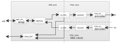
UART 由多个子模块组成,提供以下功能:
dma_intf
DMA 控制单元
与 GDMA 模块的接口
tx_fifo
UART0/1 为 16 × 11 位 entries
UART2_BT 为 32 × 11 位 entries
rx_fifo
UART0/1 为 64 × 11 位 entries
UART2_BT 为 32 × 11 位 entries
tx_fifo
UART0/1/2 为 16 × 11 位 entries
UART3_BT 为 32 × 11 位 entries
rx_fifo
UART0/1/2 为 64 × 11 位 entries
UART3_BT 为 32 × 11 位 entries
tx_fifo
UART0/1/2 为 16 × 11 位 entries
UART3_BT 为 32 × 11 位 entries
rx_fifo
UART0/1/2 为 64 × 11 位 entries
UART3_BT 为 32 × 11 位 entries
tx_fifo
UART0/1/2 为 16 × 11 位 entries
UART3_BT 为 32 × 11 位 entries
rx_fifo
UART0/1/2 为 64 × 11 位 entries
UART3_BT 为 32 × 11 位 entries
tx_fifo
UART0/1/2 为 16 × 11 位 entries
UART3_BT 为 32 × 11 位 entries
rx_fifo
UART0/1/2 为 64 × 11 位 entries
UART3_BT 为 32 × 11 位 entries
tx_fifo
UART0/1/2 为 16 × 11 位 entries
UART3_BT 为 32 × 11 位 entries
rx_fifo
UART0/1/2 为 64 × 11 位 entries
UART3_BT 为 32 × 11 位 entries
tx_fifo
UART0/1 为 16 × 11 位 entries
UART2/UART3_BT 为 32 × 11 位 entries
rx_fifo
UART0/1 为 64 × 11 位 entries
UART2/UART3_BT 为 32 × 11 位 entries
tx_fifo
UART0/1 为 16 × 11 位 entries
UART2 为 32 × 11 位 entries
rx_fifo
UART0/1 为 64 × 11 位 entries
UART2 为 32 × 11 位 entries
xmitckt
移位寄存器
生成 UART 格式数据
支持分数波特率
irda_sir_encoder
UART Tx 数据的 SIR 编码器
recvckt
接收 UART 格式数据
错误检测
中断控制
支持分数波特率
用于低功耗的振荡器时钟
监控和消除 Rx 波特率误差和自身频率漂移
irda_sir_decoder
UART Rx 数据的 SIR 解码器
apb_slv_wrap
APB3 总线接口
regmng
寄存器控制单元
功能描述
本节主要介绍 UART 模块的功能与操作原理。
UART 串行协议
由于 UART 与通信对端之间的串行通信是异步的,因此需要在数据流中添加额外的同步位(起始位和停止位)来指示有效数据的开始和结束。这种由起始位、数据位和停止位组成的串行数据封装结构通常被称为字符帧,如下图所示。

串行数据格式
为了提供基础的接收数据检错能力,还可以在字符帧中添加一个可选的奇偶校验位。该位出现在字符结构中的最后一个数据位之后、停止位之前。
UART 串行字符帧的具体特性由 UART 线控制寄存器(Line Control Register, LCR)统一配置。标准的数据传输顺序如下:
起始位:指示通信开始。
数据位:紧随起始位之后发送(可配置为 7 位或 8 位),并始终从最低有效位 (LSB) 开始传输。
校验位 (可选):紧接数据位之后,支持奇校验、偶校验或粘滞校验 (Sticky parity)。
停止位:指示该帧结束,可配置为 1 位或 2 位。
波特率计算
Tx 路径和 Rx 路径的波特率计算遵循以下公式:

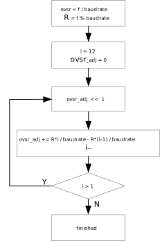
Tx 和 Rx 路径均支持分数波特率生成器。参数 ovsr[19:0] 和 ovsr_adj[10:0] 需根据模块时钟频率和目标波特率进行配置。这两个参数的具体计算过程如下图所示(其中 f 表示模块时钟频率):
为了确保通信的正确性,总波特率误差必须小于 3%。总波特率误差 ∆E 由以下三部分组成:
∆E = E1 + E2 + E3
其中
E1:发送端设备实际波特率与预期通信波特率之间的误差。
E2:接收模块时钟的频率漂移。
E3:接收设备波特率的计算误差(即 ovsr[19:0] 计算值与实际波特率之间的误差)。
对于接收端设备,可以通过监控 Rx 数据的波特率来降低 E1 和 E2,并通过使用分数波特率生成器来降低 E3。
在时钟源的选择上,建议遵循以下原则:
选择 XTAL 40MHz 时钟的 Rx 路径:如果 E1 和 E2 的最大总和较小(< 2%)。此时支持更高的波特率传输。
选择 OSC 2MHz 时钟的 Rx 路径:如果 E1 和 E2 的最大总和较大(2% ~ 4%)。虽然支持的最高波特率受限,但可以利用 OSC 时钟(±3%)实现系统的低功耗设计。
下表列出了 Tx 和 Rx 路径支持的常用波特率。对于采用 2MHz 时钟的 Rx 路径,要求 E3 < 3%。考虑到在启用 Rx 波特率监控功能时会禁用分数部分(导致最大波特率计算偏差为 0.5),因此:
ovsr[19:0] 的最小值为:0.5 / 3% ≈ 16
最大支持波特率为:2MHz / 16 = 125,000 bps
项目 |
Tx/Rx 路径(高速模式) |
Rx 路径(低功耗模式) |
|---|---|---|
时钟选择 |
XTAL 40MHz |
OSC 2MHz(±3%) |
支持的波特率(bps) |
110, 300, 600, 1200, 2400, 4800, 9600, 14400, 19200, 28800, 38400, 57600, 76800, 115200, 128000, 153600, 230400, 380400, 460800, 500000, 921600, 1000000, 1382400, 1444400, 1500000, 1843200, 2000000, 2100000, 2764800, 3000000, 3250000, 3692300, 3750000, 4000000, 6000000, 8000000 |
110, 300, 600, 1200, 2400, 4800, 9600, 14400, 19200, 28800, 38400, 57600, 76800, 115200 |
下表列出了模块时钟为 XTAL 40MHz 时不同波特率的误差率,最大误差率不超过 0.5%。
时钟 |
理论波特率 |
实际波特率 |
误差率(%) |
|---|---|---|---|
XTAL 40MHz |
110 |
110 |
0 |
XTAL 40MHz |
300 |
300 |
0 |
XTAL 40MHz |
600 |
600 |
0 |
XTAL 40MHz |
1200 |
1200 |
0 |
XTAL 40MHz |
2400 |
2400 |
0 |
XTAL 40MHz |
4800 |
4800 |
0 |
XTAL 40MHz |
9600 |
9600 |
0 |
XTAL 40MHz |
14400 |
14400 |
0 |
XTAL 40MHz |
19200 |
19200 |
0 |
XTAL 40MHz |
28800 |
28800 |
0 |
XTAL 40MHz |
38400 |
38399 |
-0.0026 |
XTAL 40MHz |
57600 |
57604 |
0.0069 |
XTAL 40MHz |
76800 |
76805 |
0.0065 |
XTAL 40MHz |
115200 |
115207 |
0.0061 |
XTAL 40MHz |
128000 |
128000 |
0 |
XTAL 40MHz |
153600 |
153610 |
0.0065 |
XTAL 40MHz |
230400 |
230415 |
0.0065 |
XTAL 40MHz |
380400 |
380228 |
-0.0452 |
XTAL 40MHz |
460800 |
460829 |
0.0063 |
XTAL 40MHz |
500000 |
500000 |
0 |
XTAL 40MHz |
921600 |
921659 |
0.0064 |
XTAL 40MHz |
1000000 |
1000000 |
0 |
XTAL 40MHz |
1382400 |
1384083 |
0.1217 |
XTAL 40MHz |
1444400 |
1444043 |
-0.0247 |
XTAL 40MHz |
1500000 |
1498127 |
-0.1249 |
XTAL 40MHz |
1843200 |
1843318 |
0.0064 |
XTAL 40MHz |
2000000 |
2000000 |
0 |
XTAL 40MHz |
2100000 |
2105263 |
0.2506 |
XTAL 40MHz |
2764800 |
2758621 |
-0.2235 |
XTAL 40MHz |
3000000 |
3007519 |
0.2506 |
XTAL 40MHz |
3250000 |
3252033 |
0.0626 |
XTAL 40MHz |
3692300 |
3703704 |
0.3089 |
XTAL 40MHz |
3750000 |
3738318 |
-0.3115 |
XTAL 40MHz |
4000000 |
4000000 |
0 |
XTAL 40MHz |
6000000 |
5970149 |
-0.4975 |
XTAL 40MHz |
8000000 |
备注
误差率的计算保留四位小数。
IrDA SIR 协议
红外数据协会(Infrared Data Association, IrDA)的串行红外(Serial Infrared, SIR)模式支持以红外光为传输媒介,与远程设备进行双向数据通信。IrDA 1.0 SIR 规范定义的最大波特率为 115.2 kbps。
其数据格式与标准通用异步收发器(Universal Asynchronous Receiver/Transmitter, UART)数据格式相似。每个数据字符采用串行传输,以 1 个起始位开始,随后跟随 7 或 8 个数据位,并以 1 或 2 个停止位结束。IrDA 模式不支持奇偶校验;若尝试通过线路控制寄存器(LCR)使能奇偶校验,将导致错误的校验位被插入到串行数据流中。当 UART 被配置为支持 IrDA 后,通过将杂项控制寄存器(MISCR)的第 0 位置 1 即可使能 IrDA 模式。
在 IrDA SIR 格式中,发送单次红外脉冲表示逻辑 0 ,无脉冲输出表示逻辑 1 。因此,每个新字符的传输均以代表起始位的红外脉冲开始。然而,接收数据在逻辑上与发送数据反相。这是因为红外脉冲会导通 IrDA 接收器中光敏三极管的基极,从而将其输出拉低。此反相输出随后被送入 UART 接收(Rx)端口,以恢复正确的 UART 信号极性。此外,通过配置 MISCR 寄存器的第 19 位和第 20 位,可以反转 IrDA 的输入与输出逻辑电平。每个红外脉冲的持续时间标称值为标准串行位时间的 3/16 。通过配置 SIR_TX_PWC0 寄存器,软件可动态调整 IrDA 发送(Tx)的脉冲宽度。下图对比了 IrDA SIR 数据格式与标准 UART 格式的时序关系。
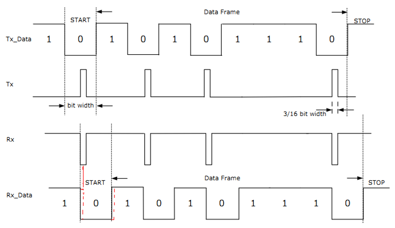
IrDA 信号与 UART 信号的关系
下表列出了本芯片所支持的串行红外(SIR)模式下,各信号速率的脉冲持续时间技术规范,其最高传输速率为 115.2 kbps。
信号速率 |
调制方式 |
速率容限 (%) |
最小脉冲持续时间 |
典型脉冲持续时间 |
最大脉冲持续时间 |
|---|---|---|---|---|---|
2.4 kbps |
RZI |
±0.87 |
1.41 us |
78.13 us |
88.85 us |
9.6 kbps |
RZI |
±0.87 |
1.41 us |
19.53 us |
22.13 us |
19.2 kbps |
RZI |
±0.87 |
1.41 us |
9.77 us |
11.07 us |
38.4 kbps |
RZI |
±0.87 |
1.41 us |
4.88 us |
5.96 us |
57.6 kbps |
RZI |
±0.87 |
1.41 us |
3.26 us |
4.34 us |
115.2 kbps |
RZI |
±0.87 |
1.41 us |
1.63 us |
2.23 us |
中断
UART 支持独立中断和组合中断请求,两者均可被屏蔽。组合中断请求是所有未屏蔽的 UART 中断进行逻辑或运算的结果。系统设计者可以选择将独立中断请求或仅将组合中断请求路由到中断控制器。UART 中断的具体描述如下:
接收数据可用中断(ERBFI) - 当达到 Rx FIFO 触发级别或 Rx FIFO 满时置位。Rx FIFO 触发级别可通过软件在 FIFO 控制寄存器(FCR,Bit [7:6])中配置,用于定义产生中断的接收 FIFO 数据量阈值。当 Rx FIFO 中的条目数减少到触发级别以下时,此中断由硬件自动清除。当此中断发生时,线路状态寄存器(LSR,Bit 8)中的 RXFIFO_INT 位将被置位。
发送器 FIFO 空中断(ETBEI) - 当 Tx FIFO 为空时置位。当数据写入 Tx FIFO 缓冲区时,此中断由硬件清除。当此中断发生时,线路状态寄存器(LSR,Bit 5)中的 TX_EMPTY 位将被置位。
接收器线路状态中断(ELSI) - 当在 Rx 线路上检测到溢出、奇偶校验错误、帧错误或中断(Break)条件时置位。此中断将保持置位状态,直到用户在中断清除寄存器(ICR)中置位接收器线路状态中断清除标志(RLSICF)。当在 Rx 线路上检测到溢出、奇偶校验错误、帧错误或中断条件时,OVR_ERR(LSR,Bit 1)、 PAR_ERR(LSR,Bit 2)、 FRM_ERR(LSR,Bit 3)和 BREAK_INT(LSR,Bit 4)位将分别置位。当上述任一事件发生时,RXFIFO_ERR(LSR,Bit 7)位也将被置位。向 RLSICF 写入
1也会同步清除 RXFIFO_ERR 状态。调制解调器状态中断(EDSSI) - 当启用硬件自动流控功能,且在 CTS 信号线上检测到下降沿时置位。此中断将保持置位状态,直到用户在 ICR 中置位调制解调器中断清除标志(MICF)。当此中断发生时,MODEM_INT(LSR,Bit 11)将被置位。
Rx 路径监控完成中断(EMDI) - 当启用 Rx 路径监控功能且监控过程结束时置位。此中断将保持置位状态,直到用户在 ICR 中置位监控完成中断清除标志(MDICF)位。当此中断发生时,MONITOR_DONE_INT(LSR,Bit 10)将被置位。
Rx 超时中断(ETOI) - 当 Rx FIFO 中至少存在一个字符时,且在设定时间超时前,没有任何字符被写入或读出 RX FIFO 时置位。此中断将保持置位状态,直到用户在 ICR 中置位超时中断清除标志(TOICF)。当此中断发生时,TIMEOUT_INT(LSR,Bit 9)将被置位。
RXFIFO 空超时中断(ERETI) - 当 Rx FIFO 持续保持空状态直至设定的时间超时后置位。此中断将保持置位状态,直到用户在 ICR 中置位 RXFIFO 空超时中断清除标志(RETICF)。当此中断发生时,RE_TIMEOUT_INT 位(LSR,Bit 13)将被置位。
Rx 噪声检测中断(ERXNDI) - 当 Rx 去抖动器(Debouncer)检测到噪声时置位。此中断将保持置位状态,直到用户在 ICR 中置位 Rx 噪声检测中断清除标志(RXNDICF)。当此中断发生时,RXND_INT(LSR,Bit 12)位将被置位。
支持 Rx 超时中断(ETOI),时间可以在 Rx 路径控制寄存器(RX_PATH_CTRL,Bit[31:16])中设置。
不支持 RXFIFO 空超时中断(ERETI)。
支持 Rx 超时中断(ETOI),时间可以在 Rx 路径控制寄存器(RX_PATH_CTRL,Bit[31:16])中设置。
不支持 RXFIFO 空超时中断(ERETI)。
支持 Rx 超时中断(ETOI),时间可以在 Rx 路径控制寄存器(RX_PATH_CTRL,Bit[31:16])中设置。
不支持 RXFIFO 空超时中断(ERETI)。
支持 Rx 超时中断(ETOI),时间可以在 Rx 路径控制寄存器(RX_PATH_CTRL,Bit[31:16])中设置。
不支持 RXFIFO 空超时中断(ERETI)。
支持 Rx 超时中断(ETOI),时间可以在 Rx 路径控制寄存器(RX_PATH_CTRL,Bit[31:16])中设置。
不支持 RXFIFO 空超时中断(ERETI)。
支持 Rx 超时中断(ETOI),时间可以在 Rx 路径控制寄存器(RX_PATH_CTRL,Bit[31:16])中设置。
不支持 RXFIFO 空超时中断(ERETI)。
支持 Rx 超时中断(ETOI),时间可以在 Rx 路径控制寄存器(RX_PATH_CTRL,Bit[31:16])中设置。
支持 RXFIFO 空超时中断(ERETI),时间可以在 RXFIFO 空中断超时阈值寄存器(TH_RETI,Bit[27:0])中设置。
支持 Rx 超时中断(ETOI),时间可以在 Rx 超时阈值寄存器(RXTO_THRS,Bit[27:0])中设置。
支持 RXFIFO 空超时中断(ERETI),时间可以在 Rx 超时阈值寄存器(RXTO_THRS,Bit[27:0])中设置。
自动流控
通过 nCTS 输入和 nRTS 输出,可以控制两台设备之间的串行 UART 数据流。下图显示了如何在自动流控模式下连接这两台设备:
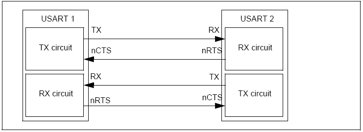
当使能自动流控模式时,如果在 Tx 空闲状态下输入 nCTS 信号被置为无效(de-asserted),则不会发生传输;如果在传输过程中输入 nCTS 信号被置为无效,则发送器会在当前传输完成后才停止发送。当 Rx FIFO 接近满载时,nRTS 信号会被置为无效,以通知对端设备在当前字符传输结束时停止发送。
UART 可配置为工作在硬件数据流控模式下,该模式由自动 RTS 和自动 CTS 两部分组成。通过置位调制解调器控制寄存器(MCR,bit5)中的 AFE 位,即可使能自动流控功能。自动 RTS 和自动 CTS 的说明如下:
自动 RTS (Auto RTS)
当满足以下所有条件时,自动 RTS 将被激活:
已使能自动流控(MCR[5] 被置 1)
已使能 RTS 输出(MCR[1] 被置 1)
已使能 FIFO(FCR[0] 被置 1)
当自动 RTS 被使能(激活)时,一旦接收 FIFO 数据量达到触发阈值(Rx_FIFO_Trigger_Level),RTS 信号将被自动强制切换为非激活状态(高电平)。
可选的接收 FIFO 阈值包括:1、1/4、1/2 以及 满值减 2。由于在 RTS 变为非激活状态后,可能仍有一个额外的字符被发送到本端 UART(这是因为对端 UART 的发送模块在识别到 RTS 取消激活之前,数据已进入发送阶段,详见 Auto RTS 时序),因此将阈值设置为 满值减 2 可以充分利用 FIFO,并保留一个字符的安全缓冲空间。
当通过读取接收缓冲寄存器(RBR_OR_THR)使 Rx FIFO 完全为空时,RTS 信号将再次变为激活状态(低电平),以通知对端 UART 继续发送数据。
当通过读取接收缓冲寄存器(RBR_OR_THR)使 Rx FIFO 完全为空时,RTS 信号将再次变为激活状态(低电平),以通知对端 UART 继续发送数据。
当通过读取接收缓冲寄存器(RBR_OR_THR)使 Rx FIFO 完全为空时,RTS 信号将再次变为激活状态(低电平),以通知对端 UART 继续发送数据。
当通过读取接收缓冲寄存器(RBR_OR_THR)使 Rx FIFO 完全为空时,RTS 信号将再次变为激活状态(低电平),以通知对端 UART 继续发送数据。
当通过读取接收缓冲寄存器(RBR_OR_THR)使 Rx FIFO 完全为空时,RTS 信号将再次变为激活状态(低电平),以通知对端 UART 继续发送数据。
当通过读取接收缓冲寄存器(RBR_OR_THR)使 Rx FIFO 完全为空时,RTS 信号将再次变为激活状态(低电平),以通知对端 UART 继续发送数据。
一旦 Rx FIFO 中的数据量降至 (Rx_FIFO_Trigger_Level - 2) 以下(通过读取接收缓冲寄存器 RBR_OR_THR 完成),RTS 信号将再次变为激活状态(低电平),以通知对端 UART 继续发送数据。
一旦 Rx FIFO 中的数据量降至 (Rx_FIFO_Trigger_Level - 2) 以下(通过读取接收缓冲寄存器 RBR_OR_THR 完成),RTS 信号将再次变为激活状态(低电平),以通知对端 UART 继续发送数据。
备注
即使已选择其他所有选项并正确设置了 MCR 的相关位,如果通过 FCR[0] 禁用了 FIFO,自动流控功能也会随之失效。当自动 RTS 未实现或被禁用时,RTS 信号仅由 MCR[1] 控制。
下图显示了自动 RTS 操作的时序图:

Auto RTS 时序
自动 CTS (Auto CTS)
当满足以下所有条件时,自动 CTS 将被激活:
已使能自动流控(MCR[5] 被置 1)
已使能 FIFO(FCR[0] 被置 1)
已禁用 SIR 模式(MISCR[0] 被清 0)
当自动 CTS 被使能(激活)时,一旦 CTS 输入信号变为非激活状态(高电平),UART 发送器将被自动禁用。这可以防止接收设备(如对端 UART)的 FIFO 发生溢出。如果在发送最后一个停止位过半之前 CTS 输入信号未被禁用,则发送器在被禁用前会额外发送一个字符。当发送器被禁用时,系统仍可向发送器 FIFO 中写入数据,这可能会导致溢出。
通过读取 UART 线路状态寄存器(LSR)来检查发送 FIFO 是否已满(LSR[6] = 0)。
当使用“FIFO 满”状态指示时,软件可以在每次向发送 FIFO 写入数据前轮询该状态。当 CTS 输入信号再次变为激活状态(低电平)时,传输将自动恢复。
备注
即使已使能了所有其他功能,如果通过 FCR[0] 禁用了 FIFO,自动流控也会随之失效。当自动 CTS 未实现或被禁用时,发送器将不受 CTS 信号状态的影响。
下图显示了自动 CTS 操作的时序图:

Auto CTS 时序
备注
受限于 SoC 引脚数量,并非所有的 UART 接口都支持 RTS/CTS 引脚。具体细节请参考相应芯片的数据手册。未引出 RTS/CTS 的串口无法使用其流控功能。
DMA 流控
对于 UART Tx,始终由 GDMA 作为 DMA 流控制器;而对于 UART Rx,GDMA 或 UART 均可作为 DMA 流控制器。注意: 本节仅说明 Rx DMA 模式。
GDMA 作为 DMA 流控制器
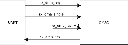
当 GDMA 作为 DMA 流控制器时(如下图所示),需要在数据块传输开始前设置期望的块长度,并在 Rx 接收长度等于该块长度时终止传输。当 Rx FIFO 中的数据量大于或等于突发大小(Burst Size) 时,rx_dma_req 信号被置为有效;当 Rx FIFO 不为空时,rx_dma_single 信号被置为有效。在当前事务中最后一个 AHB 传输(单次或突发)的数据阶段完成后,rx_dma_ack 信号被置为有效。当 GDMA 作为流控制器时,硬件不会对 rx_dma_last 信号进行采样,该信号将被忽略。
GDMA 作为 DMA 流控制器
当 GDMA 作为 DMA 流控制器时(如下图所示),需要在数据块传输开始前设置期望的块长度,并在 Rx 接收长度等于该块长度时终止传输。当 Rx FIFO 中的数据量大于或等于突发大小(Burst Size) 时,rx_dma_req 信号被置为有效;当 Rx FIFO 不为空时,rx_dma_single 信号被置为有效。在当前事务中最后一个 AHB 传输(单次或突发)的数据阶段完成后,rx_dma_ack 信号被置为有效。当 GDMA 作为流控制器时,硬件不会对 rx_dma_last 信号进行采样,该信号将被忽略。
GDMA 作为 DMA 流控制器
当 GDMA 作为 DMA 流控制器时(如下图所示),需要在数据块传输开始前设置期望的块长度,并在 Rx 接收长度等于该块长度时终止传输。当 Rx FIFO 中的数据量大于或等于突发大小(Burst Size) 时,rx_dma_req 信号被置为有效;当 Rx FIFO 不为空时,rx_dma_single 信号被置为有效。在当前事务中最后一个 AHB 传输(单次或突发)的数据阶段完成后,rx_dma_ack 信号被置为有效。当 GDMA 作为流控制器时,硬件不会对 rx_dma_last 信号进行采样,该信号将被忽略。
GDMA 作为 DMA 流控制器
当 GDMA 作为 DMA 流控制器时(如下图所示),需要在数据块传输开始前设置期望的块长度,并在 Rx 接收长度等于该块长度时终止传输。当 Rx FIFO 中的数据量大于或等于突发大小(Burst Size) 时,rx_dma_req 信号被置为有效;当 Rx FIFO 不为空时,rx_dma_single 信号被置为有效。在当前事务中最后一个 AHB 传输(单次或突发)的数据阶段完成后,rx_dma_ack 信号被置为有效。当 GDMA 作为流控制器时,硬件不会对 rx_dma_last 信号进行采样,该信号将被忽略。
GDMA 作为 DMA 流控制器
当 GDMA 作为 DMA 流控制器时(如下图所示),需要在数据块传输开始前设置期望的块长度,并在 Rx 接收长度等于该块长度时终止传输。当 Rx FIFO 中的数据量大于或等于突发大小(Burst Size) 时,rx_dma_req 信号被置为有效;当 Rx FIFO 不为空时,rx_dma_single 信号被置为有效。在当前事务中最后一个 AHB 传输(单次或突发)的数据阶段完成后,rx_dma_ack 信号被置为有效。当 GDMA 作为流控制器时,硬件不会对 rx_dma_last 信号进行采样,该信号将被忽略。
GDMA 作为 DMA 流控制器
当 GDMA 作为 DMA 流控制器时(如下图所示),需要在数据块传输开始前设置期望的块长度,并在 Rx 接收长度等于该块长度时终止传输。当 Rx FIFO 中的数据量大于或等于突发大小(Burst Size) 时,rx_dma_req 信号被置为有效;当 Rx FIFO 不为空时,rx_dma_single 信号被置为有效。在当前事务中最后一个 AHB 传输(单次或突发)的数据阶段完成后,rx_dma_ack 信号被置为有效。当 GDMA 作为流控制器时,硬件不会对 rx_dma_last 信号进行采样,该信号将被忽略。
GDMA 作为 DMA 流控制器
当 GDMA 作为 DMA 流控制器时(如下图所示),需要在数据块传输开始前设置期望的块长度,并在 Rx 接收长度等于该块长度时终止传输。当 Rx FIFO 中的数据量大于或等于突发大小(Burst Size) 时,rx_dma_req 信号被置为有效;当 Rx FIFO 不为空时,rx_dma_single 信号被置为有效。在当前事务中最后一个 AHB 传输(单次或突发)的数据阶段完成后,rx_dma_ack 信号被置为有效。当 GDMA 作为流控制器时,硬件不会对 rx_dma_last 信号进行采样,该信号将被忽略。
GDMA 作为 DMA 流控制器
具体来说,当数据传输不可预测时(例如 Rx 数据量未知),建议将 GDMA 设置为流控制器:
UART Rx 突发大小和 GDMA 突发事务大小均应设置为 1。GDMA 块传输大小应设置为大于预期数据量的值,或直接设置为 65535(最大值)。此外,应启用 RXFIFO 空超时中断(ERETI),以通知事务已暂停一段时间。
一旦 RXFIFO 空超时中断(ERETI)被触发,RXDMA_EN 将被硬件自动清除,即使有新数据进入 RX FIFO,也不会发出 DMA 请求。可以通过寄存器 UART_RX_BYTE_CNT 获取 DMA 从 RX FIFO 读取的字节数。如果中断发生后有新数据到达,用户可以手动读取 RX FIFO 中的剩余数据。用户还应禁用 DMA。
当 GDMA 作为 DMA 流控制器时(如下图所示),需要在数据块传输开始前设置期望的块长度,并在 Rx 接收长度等于该块长度时终止传输。当 Rx FIFO 中的数据量大于或等于突发大小(Burst Size) 时,rx_dma_req 信号被置为有效;当 Rx FIFO 不为空时,rx_dma_single 信号被置为有效。在当前事务中最后一个 AHB 传输(单次或突发)的数据阶段完成后,rx_dma_ack 信号被置为有效。当 GDMA 作为流控制器时,硬件不会对 rx_dma_last 信号进行采样,该信号将被忽略。
GDMA 作为 DMA 流控制器
具体来说,当数据传输不可预测时(例如 Rx 数据量未知),建议将 GDMA 设置为流控制器:
UART Rx 突发大小和 GDMA 突发事务大小均应设置为 1。GDMA 块传输大小应设置为大于预期数据量的值,或直接设置为 65535(最大值)。此外,应启用 RXFIFO 空超时中断(ERETI),以通知事务已暂停一段时间。
一旦 RXFIFO 空超时中断(ERETI)被触发,RXDMA_EN 将被硬件自动清除,即使有新数据进入 RX FIFO,也不会发出 DMA 请求。可以通过寄存器 UART_RX_BYTE_CNT 获取 DMA 从 RX FIFO 读取的字节数。如果中断发生后有新数据到达,用户可以手动读取 RX FIFO 中的剩余数据。用户还应禁用 DMA。
UART 作为 DMA 流控制器
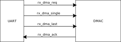
当 UART 作为 DMA 流控制器时(如下图所示),若 UART 已接收完所有数据,它会将 rx_dma_last 信号拉高,以终止块传输。传输结束的触发条件为:在接收到最后一个字符后,经过 UART_RX_PATH_CTRL 寄存器中配置的 UART_RX_BYTE_CNT 时间内,没有新的字符输入。
当 UART 作为 DMA 流控制器时(如下图所示),若 UART 已接收完所有数据,它会将 rx_dma_last 信号拉高,以终止块传输。传输结束的触发条件为:在接收到最后一个字符后,经过 UART_RX_PATH_CTRL 寄存器中配置的 UART_RX_BYTE_CNT 时间内,没有新的字符输入。
当 UART 作为 DMA 流控制器时(如下图所示),若 UART 已接收完所有数据,它会将 rx_dma_last 信号拉高,以终止块传输。传输结束的触发条件为:在接收到最后一个字符后,经过 UART_RX_PATH_CTRL 寄存器中配置的 UART_RX_BYTE_CNT 时间内,没有新的字符输入。
当 UART 作为 DMA 流控制器时(如下图所示),若 UART 已接收完所有数据,它会将 rx_dma_last 信号拉高,以终止块传输。传输结束的触发条件为:在接收到最后一个字符后,经过 UART_RX_PATH_CTRL 寄存器中配置的 UART_RX_BYTE_CNT 时间内,没有新的字符输入。
当 UART 作为 DMA 流控制器时(如下图所示),若 UART 已接收完所有数据,它会将 rx_dma_last 信号拉高,以终止块传输。传输结束的触发条件为:在接收到最后一个字符后,经过 UART_RX_PATH_CTRL 寄存器中配置的 UART_RX_BYTE_CNT 时间内,没有新的字符输入。
当 UART 作为 DMA 流控制器时(如下图所示),若 UART 已接收完所有数据,它会将 rx_dma_last 信号拉高,以终止块传输。传输结束的触发条件为:在接收到最后一个字符后,经过 UART_RX_PATH_CTRL 寄存器中配置的 UART_RX_BYTE_CNT 时间内,没有新的字符输入。
当 UART 作为 DMA 流控制器时(如下图所示),若 UART 已接收完所有数据,它会将 rx_dma_last 信号拉高,以终止块传输。传输结束的触发条件为:在接收到最后一个字符后,经过 UART_RX_PATH_CTRL 寄存器中配置的 UART_RX_BYTE_CNT 时间内,没有新的字符输入。
当 UART 作为 DMA 流控制器时(如下图所示),若 UART 已接收完所有数据,它会将 rx_dma_last 信号拉高,以终止块传输。传输结束的触发条件为:在接收到最后一个字符后,经过 UART_RXTO_THRS 寄存器中配置的 UART_R_RXTO_THRS 时间内,没有新的字符输入;或者通过 UART 接收的总数据量达到了 UART_RXDMA_MAX_LEN 配置的最大字节数限制。
在 rx_dma_req 信号被拉高之前,UART 将计算待传输的数据量,并执行以下操作:
如果待传输的数据量小于 DMA Rx 突发大小,则会通过拉高 rx_dma_single 信号,在单次 DMA 事务中传输所有剩余数据。当只剩一个字节的数据需要传输时,将会拉高 rx_dma_last 信号,最后一个字节将通过 DMA 传输到目标内存。
传输过程中,可以通过 UART_RXDMA_REMAIN_LEN 寄存器检查剩余的可接收字节数。当 DMA 传输完成(rx_dma_last=1)或 rx_dma_en 被禁用时,该寄存器将被重置为 UART_RXDMA_MAX_LEN 的值。
UART 为 DMA 流控制器
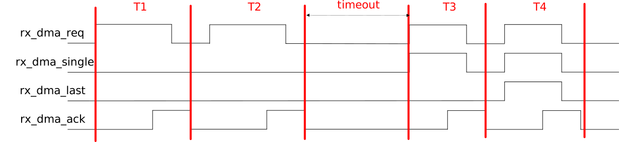
下图展示了在总接收数据长度不是突发事务大小倍数时的 DMA 接口时序。T1 和 T2 为突发传输,T3 和 T4 为单次传输。其中 T2 是该块传输的最后一次突发传输。超时发生后,Rx FIFO 中仅剩两个条目(小于突发事务传输大小)。随后 UART 启动两次单次传输(T3 和 T4)来完成该数据块传输。rx_dma_last 信号伴随最后一个 rx_dma_req 信号一起发送给 GDMA。在这种情况下,超时后可能会触发多次单次传输。
DMA 接口时序图(块大小不是突发事务大小的倍数)
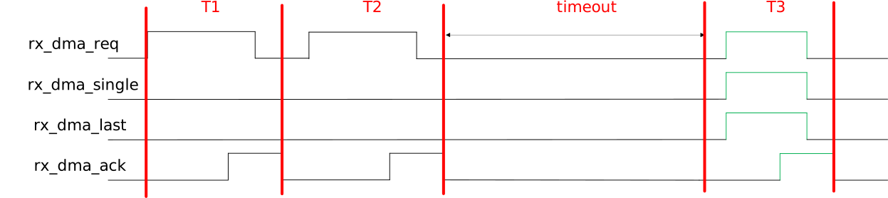
下图展示了在总接收数据长度是突发事务大小倍数时的 DMA 接口时序。此时,数据块传输实际上在 T2 的最后一次突发传输之后就已经完成了。但是,UART 无法立刻判断块传输已结束,直到超时条件发生。在 T3 阶段,UART 会启动一次伪单次传输(Dummy Transfer)以通知 GDMA,同时在 MISCR 寄存器中设置 DUMMY_FLAG 为供软件判断。伪数据可以通过 MISCR 寄存器中的 DUMMY_DATA 字段进行配置。
DMA 接口时序图(块大小是突发事务大小的倍数)
低功耗 Rx 模式
UART0、UART1、UART2_BT 和 LOGUART 的 Rx 路径时钟结构相似。下图展示了 UARTx Rx 的时钟结构(其中 x 取值范围为 0 到 2)。REG_CKSL_GRP0 寄存器中的 cksl_uart 信号决定了 UARTx Rx 路径的时钟。
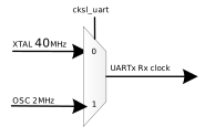
在低功耗状态下:
支持 OSC2M 时钟(由 OSC4M 分频)作为 UART Rx 时钟以唤醒系统;
XTAL40M 被直接门控(gated)。如果使用 XTAL40M 时钟作为 UART Rx 时钟,系统无法被唤醒。
备注
通过 UART 唤醒系统,需将 PMC_BIT_PST_SLEP_ERCK 设置为 1,以确保 sleep 期间 cke_uartx 为 1。
UART0、UART1、UART2、UART3_BT 和 LOGUART 的 Rx 路径时钟结构相似。下图展示了 UARTx Rx 的时钟结构(其中 x 取值范围为 0 到 3)。REG_CKSL_GRP0 寄存器中的 cksl_uart 信号决定 UARTx Rx 路径的时钟。
系统进入低功耗状态后,可以向 UART 发送数据,利用 UART 中断唤醒系统。
低功耗状态下,支持 XTAL40M/OSC2M 时钟作为 UART Rx 时钟,此时系统可以被唤醒。
如果选择 XTAL40M/OSC2M 作为时钟源,PMC_MASK_PST_SLEP_XMD 需要设置为 0x3(normal)。
UART0、UART1、UART2、UART3_BT 和 LOGUART 的 Rx 路径时钟结构相似。下图展示了 UARTx Rx 的时钟结构(其中 x 取值范围为 0 到 3)。REG_CKSL_GRP0 寄存器中的 cksl_uart 信号决定 UARTx Rx 路径的时钟。
系统进入低功耗状态后,可以向 UART 发送数据,利用 UART 中断唤醒系统。
低功耗状态下,支持 XTAL40M/OSC2M 时钟作为 UART Rx 时钟,此时系统可以被唤醒。
如果选择 XTAL40M/OSC2M 作为时钟源,PMC_MASK_PST_SLEP_XMD 需要设置为 0x3(normal)。
UART0、UART1、UART2、UART3_BT 和 LOGUART 的 Rx 路径时钟结构相似。下图展示了 UARTx Rx 的时钟结构(其中 x 取值范围为 0 到 3)。REG_CKSL_GRP0 寄存器中的 cksl_uart 信号决定 UARTx Rx 路径的时钟。
系统进入低功耗状态后,可以向 UART 发送数据,利用 UART 中断唤醒系统。
低功耗状态下,支持 XTAL40M/OSC2M 时钟作为 UART Rx 时钟,此时系统可以被唤醒。
如果选择 XTAL40M/OSC2M 作为时钟源,PMC_MASK_PST_SLEP_XMD 需要设置为 0x3(normal)。
UART0、UART1、UART2、UART3_BT 和 LOGUART 的 Rx 路径时钟结构相似。下图展示了 UARTx Rx 的时钟结构(其中 x 取值范围为 0 到 3)。REG_CKSL_GRP0 寄存器中的 cksl_uart 信号决定 UARTx Rx 路径的时钟。
系统进入低功耗状态后,可以向 UART 发送数据,利用 UART 中断唤醒系统。
低功耗状态下,支持 XTAL40M/OSC2M 时钟作为 UART Rx 时钟,此时系统可以被唤醒。
如果选择 XTAL40M/OSC2M 作为时钟源,PMC_MASK_PST_SLEP_XMD 需要设置为 0x3(normal)。
UART0、UART1、UART2 和 LOGUART 的 Rx 路径时钟结构相似。下图展示了 UARTx Rx 的时钟结构(其中 x 取值范围为 0 到 2)。REG_CKSL_GRP0 寄存器中的 cksl_uart 信号和 cksl_uart2m 信号共同决定 UARTx Rx 路径的时钟。UART3_BT 的 Rx 时钟始终为 XTAL40M。
系统进入低功耗状态后,可以向 UART 发送数据,利用 UART 中断唤醒系统。
低功耗状态下,支持 XTAL40M/OSC2M 时钟作为 UART Rx 时钟,此时系统可以被唤醒。
如果选择 XTAL40M 作为时钟源,PMC_MASK_PST_SLEP_XMD 需要设置为 0x3(normal);
如果选择 OSC2M 作为时钟源,需要设置 PMC_BIT_PST_SLEP_ERCK 为 1。
UART0、UART1、UART2、UART3_BT 和 LOGUART 的 Rx 路径时钟结构相似。下图展示了 UARTx Rx 的时钟结构(其中 x 取值范围为 0 到 3)。REG_CKSL_GRP1 寄存器中的 cksl_uart 信号决定 UARTx Rx 路径的时钟。
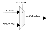
系统进入低功耗状态后,可以向 UART 发送数据,利用 UART 中断唤醒系统。
低功耗状态下,支持 XTAL40M/OSC2M 时钟作为 UART Rx 时钟,此时系统可以被唤醒。
若要使用 XTAL40M 作为 UART Rx 时钟,需在 ameba_sleepcfg.c 中将 ps_config 中的 keep_osc4m_on 和 sleep_to_08V 设置为 TRUE,并将 xtal_mode_in_sleep 设置为合适的值(如 XTAL_LPS_With_40M);
若要使用 OSC2M 作为 UART Rx 时钟,需在 ameba_sleepcfg.c 中将 ps_config 中的 keep_osc4m_on 设置为 TRUE。
UART0、UART1、UART2 和 LOGUART 的 Rx 路径时钟结构相似。下图展示了 UARTx Rx 的时钟结构(其中 x 取值范围为 0 到 2)。REG_CKSL_GRP1 寄存器中的 cksl_uart 信号决定 UARTx Rx 路径的时钟。
系统进入低功耗状态后,可以向 UART 发送数据,利用 UART 中断唤醒系统。
低功耗状态下,支持 XTAL40M/OSC2M 时钟作为 UART Rx 时钟,此时系统可以被唤醒。
若要使用 XTAL40M 作为 UART Rx 时钟,需在 ameba_sleepcfg.c 中将 ps_config 中的 keep_osc4m_on 和 sleep_to_08V 设置为 TRUE,并将 xtal_mode_in_sleep 设置为合适的值(如 XTAL_LPS_With_40M);
若要使用 OSC2M 作为 UART Rx 时钟,需在 ameba_sleepcfg.c 中将 ps_config 中的 keep_osc4m_on 设置为 TRUE。
Rx 路径监控功能
UART Rx 路径支持分数波特率发生器,它可以检测并消除 Rx 波特率误差以及自身的频率漂移。分数波特率和波特率检测控制功能不能同时使用。
当启用检测控制功能时(通过配置寄存器 UART_MON_BAUD_CTRL[0]),软件首先根据默认波特率设置原始周期数。随后, Rx 电路会计算 N 个数据位持续时间对应的总周期数 M(其中 N 的最大值为 127),由此得出每个数据位持续时间的平均周期数 L = M/N。硬件将使用新计算出的值 L 替换每个位的原始周期数,通过这种动态校准机制,可以最大程度地消除来自对端设备的波特率误差以及自身的频率偏差。
备注
当启用 Rx 路径检测控制功能时,波特率不应大于当前 LP 时钟频率的 1/17。
UART Rx 去抖动
UART 支持 Rx 去抖动(Debounce)功能,用于过滤 Rx 信号中的毛刺。将 UART_RXDBCR 寄存器中的 DBNC_FEN 位置 1 即可使能该功能。Rx 去抖动的时钟源与 Rx 时钟源相同,支持配置为 XTAL 40MHz 或 OSC 2MHz。此外,可以通过配置 UART_RXDBCR 寄存器中的 DBNC_CYC 字段来设定去抖动周期,从而过滤不同宽度的毛刺信号。
当 DBNC_FEN 位被置 1 时,持续时间短于 DBNC_CYC 个去抖动时钟周期的毛刺将被自动过滤(如下图所示)。启用该功能后,Rx 信号将引入 (DBNC_CYC + 2) 个去抖动时钟周期的延迟。
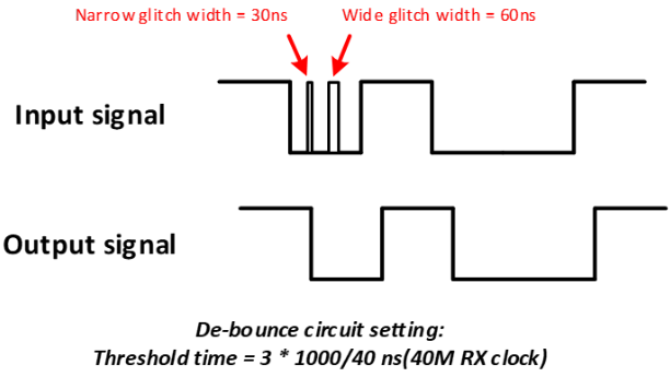
UART Rx 去抖动
UARTx_BT 作为普通 UART 使用
UART 支持通过配置,内部连接至蓝牙(BT)模块进行通信;同时,也可将其配置为普通 UART 接口,与外部设备进行通信。
备注
该功能 随芯片型号而异,并非所有型号均支持 。
标准 UART 模式与蓝牙(BT)功能 互斥 ,仅在不使用蓝牙功能时,方可将相关控制器配置为标准 UART 模式。
UART2_BT 默认被用作内部 BT UART。
如果需要将其作为普通 UART 使用,请参考下文描述,配置相关的寄存器。
名称:REG_LSYS_BT_CTRL0
大小:32 位
基地址:
0x41008000地址偏移:
0x280读/写访问:读/写
Bit |
Name |
Access |
Reset |
Description |
|---|---|---|---|---|
19 |
BT_USE_EXT_UART |
R/W |
0x0 |
|
UART3_BT 默认用于内部 BT UART。
如果需要将其作为普通 UART 使用,请参考下文描述,配置相关的寄存器。
名称:REG_LSYS_BT_CTRL0
大小:32 位
基地址:
0x4100C000地址偏移:
0x280读/写访问:读/写
Bit |
Name |
Access |
Reset |
Description |
|---|---|---|---|---|
19 |
BT_USE_EXT_UART |
R/W |
0x0 |
|
UART3_BT 默认用于内部 BT UART。
如果需要将其作为普通 UART 使用,请参考下文描述,配置相关的寄存器。
名称:REG_LSYS_BT_CTRL0
大小:32 位
基地址:
0x4100C000地址偏移:
0x280读/写访问:读/写
Bit |
Name |
Access |
Reset |
Description |
|---|---|---|---|---|
19 |
BT_USE_EXT_UART |
R/W |
0x0 |
|
UART3_BT 默认用于内部 BT UART。
如果需要将其作为普通 UART 使用,请参考下文描述,配置相关的寄存器。
名称:REG_LSYS_BT_CTRL0
大小:32 位
基地址:
0x4100C000地址偏移:
0x280读/写访问:读/写
Bit |
Name |
Access |
Reset |
Description |
|---|---|---|---|---|
19 |
BT_USE_EXT_UART |
R/W |
0x0 |
|
UART3_BT 默认用于内部 BT UART。
如果需要将其作为普通 UART 使用,请参考下文描述,配置相关的寄存器。
名称:REG_LSYS_BT_CTRL0
大小:32 位
基地址:
0x4100C000地址偏移:
0x280读/写访问:读/写
Bit |
Name |
Access |
Reset |
Description |
|---|---|---|---|---|
19 |
BT_USE_EXT_UART |
R/W |
0x0 |
|
不支持 UARTx_BT。
UART3_BT 默认用于内部 BT UART。
如果需要将其作为普通 UART 使用,请参考下文描述,配置相关的寄存器。
名称:REG_LSYS_BT_CTRL0
大小:32 位
基地址:
0x4080A000地址偏移:
0x2B8读/写访问:读/写
Bit |
Name |
Access |
Reset |
Description |
|---|---|---|---|---|
19 |
BT_USE_EXT_UART |
R/W |
0x0 |
|
不支持 UARTx_BT。
寄存器
Base Address:
UART0_REG : 0x4100C000
UART1_REG : 0x4100D000
UART2_REG : 0x4100E000
Name |
Address offset |
Access |
Description |
|---|---|---|---|
000h |
R/W |
The low 8 bits of divisor coefficient only valid when the DLAB bit of LCR bit[7] = 1. |
|
004h |
R/W |
Generate enable and disable interrupt by the UART, only valid when the DLAB bit of LCR bit[7] = 0. |
|
008h |
R |
Interrupt source indication |
|
00Ch |
R/W |
Set the general communication parameters |
|
010h |
R/W |
It is used to perform handshaking actions with the attached device. |
|
014h |
R |
Indicate the current state of communication and errors |
|
018h |
R |
It contains information about the four incoming modem control lines on the device. |
|
01Ch |
R/W |
It is used to store Tx information. |
|
020h |
R/W |
It is used to indicate the information of Tx baud rate. |
|
024h |
R/W |
The buffers of received data/transmitted data |
|
028h |
R/W |
It is used to provide DMA and IrDA related information. |
|
02Ch |
R/W |
It is used to indicate the shift value of SIR Tx pulse. |
|
030h |
R/W |
It is used to indicate the threshold of SIR Rx pulse. |
|
034h |
R/W |
It is used to monitor the baud rate of Rx pulse. |
|
03Ch |
R |
||
040h |
R/W |
It is used to monitor the Rx baud rate error and Rx baudrate factor setting. |
|
044h |
R/W |
It is used to monitor the baud rate of Rx path. |
|
048h |
R/W |
It is used to monitor the baud rate of Rx path. |
|
04Ch |
R |
It is used to monitor the clock cycle number of Rx path. |
|
050h |
R/W |
It is used to count the number of data read from RXFIFO (byte). |
|
054h |
R/W |
||
058h |
R/W |
||
05Ch |
R/W |
Added in MP version, not exist in test chip version |
|
060h |
R |
REG_UART_DLL
Name: UART divisor length register
Size: 32
Address offset: 000h
Read/write access: R/W
The low 8 bits of divisor coefficient only valid when the DLAB bit of LCR bit[7] = 1.
Bit |
Symbol |
Access |
INI |
Description |
|---|---|---|---|---|
31:8 |
RSVD |
R |
- |
Reserved |
7:0 |
BAUD |
R/W |
0x0 |
The low 8 bits of divisor coefficient (not used) |
REG_UART_IER
Name: UART interrupt enable register
Size: 32
Address offset: 004h
Read/write access: R/W
Generate enable and disable interrupt by the UART, only valid when the DLAB bit of LCR bit[7] = 0.
Bit |
Symbol |
Access |
INI |
Description |
|---|---|---|---|---|
31:7 |
RSVD |
R |
- |
Reserved |
6 |
ERXNDI |
R/W |
0x0 |
Rx noise detected interrupt enable |
5 |
ETOI |
R/W |
0x0 |
Rx timeout interrupt enable |
4 |
EMDI |
R/W |
0x0 |
Rx path monitor done interrupt enable |
3 |
EDSSI |
R/W |
0x0 |
Modem Status Interrupt (EDSSI) (modem status transition) enable |
2 |
ELSI |
R/W |
0x0 |
Receiver Line Status Interrupt (ELSI) (receiver line status) enable |
1 |
ETBEI |
R/W |
0x0 |
Transmitter FIFO Empty interrupt (ETBEI) (Tx FIFO empty) enable |
0 |
ERBI |
R/W |
0x0 |
Received Data Available Interrupt (ERBFI) (Rx trigger) enable |
REG_UART_IIR
Name: UART interrupt identification register
Size: 32
Address offset: 008h
Read/write access: R
Interrupt source indication
Bit |
Symbol |
Access |
INI |
Description |
|---|---|---|---|---|
31:1 |
RSVD |
R |
- |
Reserved |
0 |
INT_PEND |
R |
0x1 |
|
REG_UART_LCR
Name: UART line control register
Size: 32
Address offset: 00Ch
Read/write access: R/W
Set the general communication parameters
Bit |
Symbol |
Access |
INI |
Description |
|---|---|---|---|---|
31:8 |
RSVD |
R |
- |
Reserved |
7 |
DLAB |
R/W |
0x0 |
Divisor Latch Access bit, and control the accessibility of the DLL, DLM and IER registers
备注 THR/RBR don't care the value of this bit. |
6 |
BRCTL |
R/W |
0x0 |
Break Control bit
|
5 |
STKP |
R/W |
0x0 |
Stick Parity bit
|
4 |
EPS |
R/W |
0x0 |
Even Parity selection
|
3 |
PEN |
R/W |
0x0 |
Parity Enable
|
2 |
STB |
R/W |
0x0 |
Stop bits length selection
备注 The receiver always checks the first stop bit only. |
1 |
RSVD |
R |
- |
Reserved |
0 |
WLS0 |
R/W |
0x1 |
Word length selection
|
REG_UART_MCR
Name: UART modem control register
Size: 32
Address offset: 010h
Read/write access: R/W
It is used to perform handshaking actions with the attached device.
Bit |
Symbol |
Access |
INI |
Description |
|---|---|---|---|---|
31:6 |
RSVD |
R |
- |
Reserved |
5 |
AFE |
R/W |
0x0 |
Auto flow control enable |
4 |
LOOP_EN |
R/W |
0x0 |
LoopBack mode
|
3 |
OUT2 |
R/W |
0x0 |
Auxiliary output 2 Bit[3] affects the OUT2_ output in a manner identical to that described above set to 0. In loopback mode, connected to Data Carrier Detect (DCD). |
2 |
OUT1 |
R/W |
0x0 |
Auxiliary output 1 Bit3 affects the OUT1_ output in a manner identical to that described above set to 0. In loopback mode, connected to Ring Indicator (RI). |
1 |
RTS |
R/W |
0x0 |
Request to Send (RTS) signal control
This bit controls the RTS_ output. Bit[1] affects the RTS_ output in a manner identical to that described above set to 0. |
0 |
DTR |
R/W |
0x0 |
This bit controls the DTR output. |
REG_UART_LSR
Name: UART line status register
Size: 32
Address offset: 014h
Read/write access: R
Indicate the current state of communication and errors
Bit |
Symbol |
Access |
INI |
Description |
|---|---|---|---|---|
31:13 |
RSVD |
R |
- |
Reserved |
12 |
RXND_INT |
R |
0 |
This bit is only set when Rx debouncer has detected noise.
|
11 |
MODEM_INT |
R |
0 |
This bit is only set when Modem status is pending.
|
10 |
MONITOR_DONE_INT |
R |
0 |
This bit is only set when Rx Path Monitor Done interrupt is enabled (EMDI is set).
|
9 |
TIMEOUT_INT |
R |
0 |
This bit is only set when Rx Timeout interrupt is enabled (ETOI is set).
|
8 |
RXFIFO_INT |
R |
0 |
This bit is only set when Received Data Available Interrupt interrupt is enabled (ERBI is set).
|
7 |
RXFIFO_ERR |
R |
0 |
Uart_rx_error, depending on the FIFO control register (FCR) bit[0]
|
6 |
TX_NOT_FULL |
R |
1 |
TXFIFO not full indicator |
5 |
TX_EMPTY |
R |
1 |
TXFIFO empty indicator |
4 |
BREAK_INT |
R |
Break Interrupt (BI) indicator
|
|
3 |
FRM_ERR |
R |
Framing Error (FE) indicator
|
|
2 |
PAR_ERR |
R |
Parity Error (PE) indicator
|
|
1 |
OVR_ERR |
R |
Overrun Error (OE) indicator
|
|
0 |
DRDY |
R |
|
REG_UART_MSR
Name: UART modem status register
Size: 32
Address offset: 018h
Read/write access: R
It contains information about the four incoming modem control lines on the device.
Bit |
Symbol |
Access |
INI |
Description |
|---|---|---|---|---|
31:8 |
RSVD |
R |
- |
Reserved |
7 |
R_DCD |
R |
Complement of the DCD input or equals to Out2 in loopback mode. |
|
6 |
R_RI |
R |
Complement of the RI input or equals to Out1 in loopback mode. |
|
5 |
R_DSR |
R |
Complement of the DSR input or equals to DTR in loopback mode. |
|
4 |
R_CTS |
R |
Complement of the CTS input or equals to RTS in loopback mode. |
|
3 |
D_DCD |
R |
|
|
2 |
TERI |
R |
|
|
1 |
D_DSR |
R |
|
|
0 |
D_CTS |
R |
|
REG_UART_SCR
Name: UART scratch pad register
Size: 32
Address offset: 01Ch
Read/write access: R/W
It is used to store Tx information.
Bit |
Symbol |
Access |
INI |
Description |
|---|---|---|---|---|
31:27 |
RSVD |
R |
- |
Reserved |
26:16 |
XFACTOR_ADJ |
R/W |
0x0 |
One factor of baud rate calculation for Tx path |
15:13 |
RSVD |
R |
- |
Reserved |
12:8 |
DBG_SEL |
R/W |
0x0 |
Debug port selection |
7 |
SCRATCH_7 |
R/W |
0x0 |
Clear Rx break signal interrupt status |
6:0 |
SCRATCH_6_0 |
R/W |
0x30 |
|
REG_UART_STS
Name: UART STS register
Size: 32
Address offset: 020h
Read/write access: R/W
It is used to indicate the information of Tx baud rate.
Bit |
Symbol |
Access |
INI |
Description |
|---|---|---|---|---|
31:24 |
RSVD |
R |
- |
Reserved |
23:4 |
XFACTOR |
R/W |
0x1047 |
Factor of baud rate calculation for Tx path |
3:0 |
RSVD |
R |
- |
Reserved |
REG_UART_RBR_OR_UART_THR
Name: UART receiver buffer register/UART transmitter holding register
Size: 32
Address offset: 024h
Read/write access: R/W
The buffers of received data/transmitted data
Bit |
Symbol |
Access |
INI |
Description |
|---|---|---|---|---|
31:8 |
RSVD |
R |
- |
Reserved |
7:0 |
DATABIT |
R/W |
0x0 |
UART_RBR's Rx data bits or UART_THR's Tx data bit[7:0] 备注 Bit[0] is the least significant bit. It is the first bit serially received/transmitted. |
REG_UART_MISCR
Name: UART MISC control register
Size: 32
Address offset: 028h
Read/write access: R/W
It is used to provide DMA and IrDA related information.
Bit |
Symbol |
Access |
INI |
Description |
|---|---|---|---|---|
31 |
RSVD |
R |
- |
Reserved |
30 |
CLR_DUMMY_FLAG |
R/W |
0x0 |
Indicate the clearing of dummy data |
29:22 |
DUMMY_DATA |
R/W |
0x0 |
Store dummy data, when UART is DMA flow controller, dummy data is padded for last RXDMA burst request. |
21 |
RXDMA_OWNER |
R/W |
0x0 |
|
20 |
IRDA_RX_INV |
R/W |
0x0 |
Irda_rx_i reverse input enable |
19 |
IRDA_TX_INV |
R/W |
0x0 |
Irda_tx_o reverse output enable |
18:11 |
RXDMA_BURSTSIZE |
R/W |
0x4 |
RXDMA burstsize, maximum value is half of rxfifo depth. |
10:3 |
TXDMA_BURSTSIZE |
R/W |
0x4 |
TXDMA burstsize, maximum value is 16. |
2 |
RXDMA_EN |
R/W |
0x0 |
RXDMA enable, valid when dma_mode in FCR is 1'b1 |
1 |
TXDMA_EN |
R/W |
0x0 |
TXDMA enable, valid when dma_mode in FCR is 1'b1 |
0 |
IRDA_ENABLE |
R/W |
0x0 |
|
REG_UART_SIR_TX_PWC0
Name: UART IRDA SIR TX pulse width control 0 register
Size: 32
Address offset: 02Ch
Read/write access: R/W
It is used to indicate the shift value of SIR Tx pulse.
Bit |
Symbol |
Access |
INI |
Description |
|---|---|---|---|---|
31 |
UPPERBOUND_SHIFTRIGHT |
R/W |
0x0 |
|
30:16 |
UPPERBOUND_SHIFTVAL |
R/W |
0x0 |
The shift value of SIR TX pulse's right edge |
15 |
LOWBOUND_SHIFTRIGHT |
R/W |
0x0 |
|
14:0 |
LOWBOUND_SHIFTVAL |
R/W |
0x0 |
The shift value of SIR TX pulse's left edge |
REG_UART_SIR_RX_PFC
Name: UART IRDA SIR Rx pulse filter control register
Size: 32
Address offset: 030h
Read/write access: R/W
It is used to indicate the threshold of SIR Rx pulse.
Bit |
Symbol |
Access |
INI |
Description |
|---|---|---|---|---|
31:16 |
RSVD |
R |
- |
Reserved |
15:1 |
R_SIR_RX_FILTER_THRS |
R/W |
0x0 |
The threshold of SIR Rx filter, Rx pulse is valid only when Rx pulse width is larger than the threshold. |
0 |
R_SIR_RX_FILTER_EN |
R/W |
0x0 |
IrDA SIR Rx filter enable |
REG_UART_BAUD_MON
Name: UART baud monitor register
Size: 32
Address offset: 034h
Read/write access: R/W
It is used to monitor the baud rate of Rx pulse.
Bit |
Symbol |
Access |
INI |
Description |
|---|---|---|---|---|
31 |
TOGGLE_MON_EN |
R/W |
0x0 |
Toggle monitor enable |
30 |
MON_DATA_VLD |
R |
Indicate valid monitoring data |
|
29:24 |
FALLING_THRESH |
R/W |
0x7 |
Indicate the threshold of Rx data rising edge |
23:12 |
MIN_LOW_PERIOD |
R |
Minimum space of consecutive logic '0' of Rx data |
|
11:0 |
MIN_FALL_SPACE |
R |
Minimum space of adjacent falling edge of Rx data |
REG_UART_DBGR
Name: UART debug register
Size: 32
Address offset: 03Ch
Read/write access: R
Bit |
Symbol |
Access |
INI |
Description |
|---|---|---|---|---|
31:0 |
DBG_UART |
R |
The output value of debug port, depending on dbg_sel value in SCR[2:0] |
REG_UART_RX_PATH_CTRL
Name: UART Rx path control register
Size: 32
Address offset: 040h
Read/write access: R/W
It is used to monitor the Rx baud rate error and Rx baudrate factor setting.
Bit |
Symbol |
Access |
INI |
Description |
|---|---|---|---|---|
31:16 |
R_RXTO_THRS |
R/W |
0x40 |
Indicate the timeout threshold of Rx path, unit in one-bit time |
15:14 |
RSVD |
R |
- |
Reserved |
13:3 |
RXBAUD_ADJ_10_0 |
R/W |
0x0 |
One factor of Baud rate calculation for Rx path, similar with xfactor_adj |
2 |
R_RST_NEWRX_N |
R/W |
0x0 |
Reset new Rx path, low active |
1:0 |
RSVD |
R |
- |
Reserved |
REG_UART_MON_BAUD_CTRL
Name: UART monitor baud rate control register
Size: 32
Address offset: 044h
Read/write access: R/W
It is used to monitor the baud rate of Rx path.
Bit |
Symbol |
Access |
INI |
Description |
|---|---|---|---|---|
31:30 |
RSVD |
R |
- |
Reserved |
29 |
R_UPD_OSC_IN_XTAL |
R/W |
0x0 |
Update parameter r_cycnum_perbit_osc (during the update of parameter r_cycnum_perbit_xtal) enable |
28:9 |
R_CYCNUM_PERBIT_OSC |
R/W |
0x0 |
Indicate the average OSC clock cycle number of one bit, for Rx path OSC clock 备注 SW sets the initial value, and HW updates it depending on the monitor result. |
8:1 |
R_BIT_NUM_THRES |
R/W |
0x0 |
Indicate the bit number threshold of one monitor period, max value is 127 |
0 |
R_MON_BAUD_EN |
R/W |
0x0 |
Monitor Rx baud enable |
REG_UART_MON_BAUD_STS
Name: UART monitor baud rate status register
Size: 32
Address offset: 048h
Read/write access: R/W
It is used to monitor the baud rate of Rx path.
Bit |
Symbol |
Access |
INI |
Description |
|---|---|---|---|---|
31:29 |
RSVD |
R |
- |
Reserved |
28:21 |
RO_MON_TOTAL_BIT |
R |
0x0 |
Indicate the number of bits actually monitored |
20 |
RO_MON_RDY |
R |
0x0 |
Indicate the finish of calculation of actual cycle number per bit, it's cleared when r_mon_baud_en is 0. |
19:0 |
R_CYCNUM_PERBIT_XTAL |
R/W |
0x0 |
Indicate the fractional xtal clock cycle number of one bit, for Rx path XTAL clock 备注 SW sets the initial value, and HW updates it depending on the monitor result. |
REG_UART_MON_CYC_NUM
Name: UART monitored cycle number register
Size: 32
Address offset: 04Ch
Read/write access: R
It is used to monitor the clock cycle number of Rx path.
Bit |
Symbol |
Access |
INI |
Description |
|---|---|---|---|---|
31:28 |
RSVD |
R |
- |
Reserved |
27:0 |
RO_MON_TOTAL_CYCLE |
R |
Indicate the number of clock cycle actually monitored |
REG_UART_RX_BYTE_CNT
Name: UART Rx data byte count register
Size: 32
Address offset: 050h
Read/write access: R/W
It is used to count the number of data read from RXFIFO (byte).
Bit |
Symbol |
Access |
INI |
Description |
|---|---|---|---|---|
31:17 |
RSVD |
R |
- |
Reserved |
16 |
CLR_RX_BYTE_CNT |
R/W |
Write 1 to clear ro_rx_byte_cnt |
|
15:0 |
RO_RX_BYTE_CNT |
R |
Count the byte number of data read from RXFIFO |
REG_UART_FCR
Name: UART FIFO control register
Size: 32
Address offset: 054h
Read/write access: R/W
Bit |
Symbol |
Access |
INI |
Description |
|---|---|---|---|---|
31:8 |
RSVD |
R |
- |
Reserved |
7:6 |
RECVTRG |
R/W |
0x3 |
Define the 16-entries Receiver FIFO Interrupt trigger level (0~15 bytes)
|
5:4 |
RSVD |
R |
- |
Reserved |
3 |
DMA_MODE |
R/W |
0x0 |
Support DMA mode (co-operate with DW DDMA in the data path) |
2 |
XMIT_CLR |
R/W |
0x0 |
Clear xmitckt |
1 |
RECV_CLR |
R/W |
0x0 |
Clear receiving |
0 |
FIFO_EN |
R/W |
0x1 |
Error report of RCVR FIFO field enable, only valid when the LSR bit[7] is set to 1. |
REG_UART_ICR
Name: UART interrupt clear register
Size: 32
Address offset: 058h
Read/write access: R/W
Bit |
Symbol |
Access |
INI |
Description |
|---|---|---|---|---|
31:5 |
RSVD |
R |
- |
Reserved |
4 |
RXNDICF |
R/W |
0x0 |
Rx noise Detected Interrupt Flag |
3 |
MDICF |
R/W |
0x0 |
Monitor Done Interrupt Flag |
2 |
MICF |
R/W |
0x0 |
Modem Interrupt Clear Flag |
1 |
TOICF |
R/W |
0x0 |
Timeout Interrupt Clear Flag |
0 |
RLSICF |
R/W |
0x0 |
Receiver Line Statue Interrupt Clear Flag Writing 1 to this bit clears PARITY_ERR, OVERRUN_ERR, FRAMING_ERR, BREAK_ERR_INT and RXFIFO_ERR in the USART_LSR register. |
REG_UART_RXDBCR
Name: UART RX debounce control register
Size: 32
Address offset: 05Ch
Read/write access: R/W
Added in MP version, not exist in test chip version
Bit |
Symbol |
Access |
INI |
Description |
|---|---|---|---|---|
31:16 |
RSVD |
R |
- |
Reserved |
15:1 |
DBNC_CYC |
R/W |
0xF |
Debounce cycles in unit of sclk |
0 |
DBNC_FEN |
R/W |
0x0 |
UART Rx debounce enable |
REG_UART_DUMMY
Name: UART Dummy Register
Size: 32
Address offset: 060h
Read/write access: R
Bit |
Symbol |
Access |
INI |
Description |
|---|---|---|---|---|
31:16 |
RSVD |
R |
- |
Reserved |
15:0 |
DUMMY |
R |
0x0 |
Reserved for HW |
Base Address:
UART0_REG : 0x41010000
UART1_REG : 0x41011000
UART2_REG : 0x41012000
UART3_REG : 0x41013000
Name |
Address offset |
Access |
Description |
|---|---|---|---|
000h |
R/W |
The low 8 bits of divisor coefficient only valid when the DLAB bit of LCR bit[7] = 1 |
|
004h |
R/W |
Generate enable and disable interrupt by the UART, only valid when the DLAB bit of LCR bit[7] = 0. |
|
008h |
R |
Interrupt source indication |
|
00Ch |
R/W |
Set the general communication parameters |
|
010h |
R/W |
It is used to perform handshaking actions with the attached device. |
|
014h |
R |
Indicate the current state of communication and errors |
|
018h |
R |
It contains information about the four incoming modem control lines on the device |
|
01Ch |
R/W |
It is used to store information of TX |
|
020h |
R/W |
Indicate the information of Tx baud rate |
|
024h |
R/W |
The buffers of received data / The buffers of transmitted data |
|
028h |
R/W |
Provide DMA and IrDA related information |
|
02Ch |
R/W |
Indicates the shift value of SIR Tx pulse |
|
030h |
R/W |
Indicates the threshold of SIR Rx pulse |
|
034h |
R/W |
Monitor the baud rate of Rx pulse |
|
03Ch |
R |
||
040h |
R/W |
Monitor the Rx baud rate error and Rx baudrate factor setting |
|
044h |
R/W |
Monitor the baud rate of Rx path |
|
048h |
R/W |
Monitor the baud rate of Rx path |
|
04Ch |
R |
Monitored clock cycle number of Rx path |
|
050h |
R/W |
Count the number of data read from rxfifo (byte) |
|
054h |
R/W |
FIFO control |
|
058h |
R/W |
Interrupt clear |
|
05Ch |
R/W |
REG_UART_DLL
Name: UART divisor length register
Size: 32
Address offset: 000h
Read/write access: R/W
The low 8 bits of divisor coefficient only valid when the DLAB bit of LCR bit[7] = 1
Bit |
Symbol |
Access |
INI |
Description |
|---|---|---|---|---|
31:8 |
RSVD |
R |
- |
Reserved |
7:0 |
BAUD |
R/W |
0x0 |
The low 8 bits of divisor coefficient (not used) |
REG_UART_IER
Name: UART interrupt enable register
Size: 32
Address offset: 004h
Read/write access: R/W
Generate enable and disable interrupt by the UART, only valid when the DLAB bit of LCR bit[7] = 0.
Bit |
Symbol |
Access |
INI |
Description |
|---|---|---|---|---|
31:7 |
RSVD |
R |
- |
Reserved |
6 |
ERXNDI |
R/W |
0x0 |
Rx noise detected interrupt enable |
5 |
ETOI |
R/W |
0x0 |
Rx timeout interrupt enable |
4 |
EMDI |
R/W |
0x0 |
Rx path monitor done interrupt enable |
3 |
EDSSI |
R/W |
0x0 |
Modem Status Interrupt (EDSSI) (modem status transition) enable |
2 |
ELSI |
R/W |
0x0 |
Receiver Line Status Interrupt (ELSI) (receiver line status) enable |
1 |
ETBEI |
R/W |
0x0 |
Transmitter FIFO Empty interrupt (ETBEI) (Tx FIFO empty) enable |
0 |
ERBI |
R/W |
0x0 |
Received Data Available Interrupt (ERBFI) (Rx trigger) enable |
REG_UART_IIR
Name: UART interrupt identification register
Size: 32
Address offset: 008h
Read/write access: R
Interrupt source indication
Bit |
Symbol |
Access |
INI |
Description |
|---|---|---|---|---|
31:1 |
RSVD |
R |
- |
Reserved |
0 |
INT_PEND |
R |
0x1 |
|
REG_UART_LCR
Name: UART line control register
Size: 32
Address offset: 00Ch
Read/write access: R/W
Set the general communication parameters
Bit |
Symbol |
Access |
INI |
Description |
|---|---|---|---|---|
31:16 |
DUMMY |
R/W |
0x00FF |
Dummy |
15:8 |
RSVD |
R |
- |
Reserved |
7 |
DLAB |
R/W |
0x0 |
Divisor Latch Access bit, and control the accessibility of the DLL, DLM and IER registers
备注 THR/RBR don't care the value of this bit. |
6 |
BRCTL |
R/W |
0x0 |
Break Control bit
|
5 |
STKP |
R/W |
0x0 |
Stick Parity bit
|
4 |
EPS |
R/W |
0x0 |
Even Parity selection
|
3 |
PEN |
R/W |
0x0 |
Parity Enable
|
2 |
STB |
R/W |
0x0 |
Stop bits length selection
备注 The receiver always checks the first stop bit only. |
1 |
RSVD |
R |
- |
Reserved |
0 |
WLS0 |
R/W |
0x1 |
Word length selection
|
REG_UART_MCR
Name: UART modem control register
Size: 32
Address offset: 010h
Read/write access: R/W
It is used to perform handshaking actions with the attached device.
Bit |
Symbol |
Access |
INI |
Description |
|---|---|---|---|---|
31:6 |
RSVD |
R |
- |
Reserved |
5 |
AFE |
R/W |
0x0 |
Auto flow control enable |
4 |
LOOP_EN |
R/W |
0x0 |
LoopBack mode
|
3 |
OUT2 |
R/W |
0x0 |
Auxiliary output 2 Bit[3] affects the OUT2_ output in a manner identical to that described above set to 0 In loopback mode, connected to Data Carrier Detect (DCD). |
2 |
OUT1 |
R/W |
0x0 |
Auxiliary output 1 Bit[3] affects the OUT1_ output in a manner identical to that described above set to 0 In loopback mode, connected to Ring Indicator (RI) |
1 |
RTS |
R/W |
0x0 |
Request to Send (RTS) signal control
This bit controls the RTS_ output. Bit[1] affects the RTS_ output in a manner identical to that described above set to 0. |
0 |
DTR |
R/W |
0x0 |
This bit controls the DTR output |
REG_UART_LSR
Name: UART line status register
Size: 32
Address offset: 014h
Read/write access: R
Indicate the current state of communication and errors
Bit |
Symbol |
Access |
INI |
Description |
|---|---|---|---|---|
31:13 |
RSVD |
R |
- |
Reserved |
12 |
RXND_INT |
R |
0 |
This bit is only set when RX debouncer has detected noise
|
11 |
MODEM_INT |
R |
0 |
This bit is only set when Modem status pending
|
10 |
MONITOR_DONE_INT |
R |
0 |
This bit is only set when Rx Path Monitor Done interrupt is enabled(EMDI is set)
|
9 |
TIMEOUT_INT |
R |
0 |
This bit is only set when Rx Timeout interrupt is enabled(ETOI is set)
|
8 |
RXFIFO_INT |
R |
0 |
This bit is only set when Received Data Available Interrupt interrupt is enabled(ERBI is set)
|
7 |
RXFIFO_ERR |
R |
0 |
Uart_rx_error, depending on the FIFO control register (FCR) bit[0]
|
6 |
TX_NOT_FULL |
R |
1 |
TXFIFO not full indicator |
5 |
TX_EMPTY |
R |
1 |
TXFIFO empty indicator |
4 |
BREAK_INT |
R |
Break Interrupt (BI) indicator
|
|
3 |
FRM_ERR |
R |
Framing Error (FE) indicator
|
|
2 |
PAR_ERR |
R |
Parity Error (PE) indicator
|
|
1 |
OVR_ERR |
R |
Overrun Error (OE) indicator
|
|
0 |
DRDY |
R |
|
REG_UART_MSR
Name: UART modem status register
Size: 32
Address offset: 018h
Read/write access: R
It contains information about the four incoming modem control lines on the device
Bit |
Symbol |
Access |
INI |
Description |
|---|---|---|---|---|
31:8 |
RSVD |
R |
- |
Reserved |
7 |
R_DCD |
R |
Complement of the DCD input or equals to Out2 in loopback mode. |
|
6 |
R_RI |
R |
Complement of the RI input or equals to Out1 in loopback mode. |
|
5 |
R_DSR |
R |
Complement of the DSR input or equals to DTR in loopback mode. |
|
4 |
R_CTS |
R |
Complement of the CTS input or equals to RTS in loopback mode. |
|
3 |
D_DCD |
R |
|
|
2 |
TERI |
R |
|
|
1 |
D_DSR |
R |
|
|
0 |
D_CTS |
R |
|
REG_UART_SCR
Name: UART scratch pad register
Size: 32
Address offset: 01Ch
Read/write access: R/W
It is used to store information of TX
Bit |
Symbol |
Access |
INI |
Description |
|---|---|---|---|---|
31:27 |
RSVD |
R |
- |
Reserved |
26:16 |
XFACTOR_ADJ |
R/W |
0x0 |
One factor of Baud rate calculation for Tx path |
15:13 |
RSVD |
R |
- |
Reserved |
12:8 |
DBG_SEL |
R/W |
0x0 |
Debug port selection |
7 |
SCRATCH_7 |
R/W |
0x0 |
Clear Rx break signal interrupt status |
6:0 |
SCRATCH_6_0 |
R/W |
0x30 |
|
REG_UART_STS
Name: UART STS register
Size: 32
Address offset: 020h
Read/write access: R/W
Indicate the information of Tx baud rate
Bit |
Symbol |
Access |
INI |
Description |
|---|---|---|---|---|
31:24 |
RSVD |
R |
- |
Reserved |
23:4 |
XFACTOR |
R/W |
0x1047 |
Factor of Baud rate calculation for Tx path |
3:0 |
RSVD |
R |
- |
Reserved |
REG_UART_RBR_OR_UART_THR
Name: UART receiver buffer register/UART transmitter holding register
Size: 32
Address offset: 024h
Read/write access: R/W
The buffers of received data / The buffers of transmitted data
Bit |
Symbol |
Access |
INI |
Description |
|---|---|---|---|---|
31:8 |
RSVD |
R |
- |
Reserved |
7:0 |
DATABIT |
R/W |
0x0 |
UART_RBR's Rx data bits or UART_THR's Tx data bit[7:0] 备注 Bit[0] is the least significant bit. It is the first bit serially received/transmitted. |
REG_UART_MISCR
Name: UART MISC control register
Size: 32
Address offset: 028h
Read/write access: R/W
Provide DMA and IrDA related information
Bit |
Symbol |
Access |
INI |
Description |
|---|---|---|---|---|
31 |
RSVD |
R |
- |
Reserved |
30 |
CLR_DUMMY_FLAG |
R/W |
0x0 |
Indicate the clearing of dummy data |
29:22 |
DUMMY_DATA |
R/W |
0x0 |
Store dummy data, when UART is DMA flow controller, dummy data is padded for last RXDMA burst request. |
21 |
RXDMA_OWNER |
R/W |
0x0 |
|
20 |
IRDA_RX_INV |
R/W |
0x0 |
Irda_rx_i reverse input enable |
19 |
IRDA_TX_INV |
R/W |
0x0 |
Irda_tx_o reverse output enable |
18:11 |
RXDMA_BURSTSIZE |
R/W |
0x4 |
RXDMA burstsize, maximum value is half of rxfifo depth. |
10:3 |
TXDMA_BURSTSIZE |
R/W |
0x4 |
TXDMA burstsize, maximum value is 16. |
2 |
RXDMA_EN |
R/W |
0x0 |
RXDMA enable, valid when dma_mode in FCR is 1'b1 |
1 |
TXDMA_EN |
R/W |
0x0 |
TXDMA enable, valid when dma_mode in FCR is 1'b1 |
0 |
IRDA_ENABLE |
R/W |
0x0 |
|
REG_UART_SIR_TX_PWC0
Name: UART IRDA SIR TX pulse width control 0 register
Size: 32
Address offset: 02Ch
Read/write access: R/W
Indicates the shift value of SIR Tx pulse
Bit |
Symbol |
Access |
INI |
Description |
|---|---|---|---|---|
31 |
UPPERBOUND_SHIFTRIGHT |
R/W |
0x0 |
|
30:16 |
UPPERBOUND_SHIFTVAL |
R/W |
0x0 |
The shift value of SIR Tx pulse's right edge |
15 |
LOWBOUND_SHIFTRIGHT |
R/W |
0x0 |
|
14:0 |
LOWBOUND_SHIFTVAL |
R/W |
0x0 |
The shift value of SIR Tx pulse's left edge |
REG_UART_SIR_RX_PFC
Name: UART IRDA SIR Rx pulse filter control register
Size: 32
Address offset: 030h
Read/write access: R/W
Indicates the threshold of SIR Rx pulse
Bit |
Symbol |
Access |
INI |
Description |
|---|---|---|---|---|
31:16 |
RSVD |
R |
- |
Reserved |
15:1 |
R_SIR_RX_FILTER_THRS |
R/W |
0x0 |
The threshold of SIR Rx filter, Rx pulse is valid only when Rx pulse width is larger than the threshold. |
0 |
R_SIR_RX_FILTER_EN |
R/W |
0x0 |
IrDA SIR Rx filter enable |
REG_UART_BAUD_MON
Name: UART baud monitor register
Size: 32
Address offset: 034h
Read/write access: R/W
Monitor the baud rate of Rx pulse
Bit |
Symbol |
Access |
INI |
Description |
|---|---|---|---|---|
31 |
TOGGLE_MON_EN |
R/W |
0x0 |
Toggle monitor enable |
30 |
MON_DATA_VLD |
R |
Indicate valid monitoring data |
|
29:24 |
FALLING_THRESH |
R/W |
0x7 |
Indicate the threshold of Rx data rising edge |
23:12 |
MIN_LOW_PERIOD |
R |
Minimum space of consecutive logic '0' of Rx data |
|
11:0 |
MIN_FALL_SPACE |
R |
Minimum space of adjacent falling edge of Rx data |
REG_UART_DBGR
Name: UART debug register
Size: 32
Address offset: 03Ch
Read/write access: R
Bit |
Symbol |
Access |
INI |
Description |
|---|---|---|---|---|
31:0 |
DBG_UART |
R |
The output value of debug port, depending on dbg_sel value in SCR[2:0] |
REG_UART_RX_PATH_CTRL
Name: UART Rx path control register
Size: 32
Address offset: 040h
Read/write access: R/W
Monitor the Rx baud rate error and Rx baudrate factor setting
Bit |
Symbol |
Access |
INI |
Description |
|---|---|---|---|---|
31:16 |
R_RXTO_THRS |
R/W |
0x40 |
Indicate the timeout threshold of Rx path, unit in one-bit time |
15:14 |
RSVD |
R |
- |
Reserved |
13:3 |
RXBAUD_ADJ_10_0 |
R/W |
0x0 |
One factor of Baud rate calculation for Rx path, similar with xfactor_adj |
2 |
R_RST_NEWRX_N |
R/W |
0x0 |
Reset new Rx path, low active |
1:0 |
RSVD |
R |
- |
Reserved |
REG_UART_MON_BAUD_CTRL
Name: UART monitor baud rate control register
Size: 32
Address offset: 044h
Read/write access: R/W
Monitor the baud rate of Rx path
Bit |
Symbol |
Access |
INI |
Description |
|---|---|---|---|---|
31:30 |
RSVD |
R |
- |
Reserved |
29 |
R_UPD_OSC_IN_XTAL |
R/W |
0x0 |
Update parameter r_cycnum_perbit_osc (during the update of parameter r_cycnum_perbit_xtal) enable |
28:9 |
R_CYCNUM_PERBIT_OSC |
R/W |
0x0 |
Indicate the average OSC clock cycle number of one bit, for Rx path OSC clk 备注 SW sets the initial value, HW updates it depending on the monitor result. |
8:1 |
R_BIT_NUM_THRES |
R/W |
0x0 |
Indicate the bit number threshold of one monitor period, max value is 127 |
0 |
R_MON_BAUD_EN |
R/W |
0x0 |
Monitor Rx baud enable |
REG_UART_MON_BAUD_STS
Name: UART monitor baud rate status register
Size: 32
Address offset: 048h
Read/write access: R/W
Monitor the baud rate of Rx path
Bit |
Symbol |
Access |
INI |
Description |
|---|---|---|---|---|
31:29 |
RSVD |
R |
- |
Reserved |
28:21 |
RO_MON_TOTAL_BIT |
R |
0x0 |
Indicate the number of bits actually monitored |
20 |
RO_MON_RDY |
R |
0x0 |
Indicate the finish of calculation of actual cycle number per bit, it's cleared when r_mon_baud_en is 0 |
19:0 |
R_CYCNUM_PERBIT_XTAL |
R/W |
0x0 |
Indicate the fractional xtal clock cycle number of one bit, for Rx path xtal clk 备注 SW sets the initial value, HW updates it depending on the monitor result. |
REG_UART_MON_CYC_NUM
Name: UART monitored cycle number register
Size: 32
Address offset: 04Ch
Read/write access: R
Monitored clock cycle number of Rx path
Bit |
Symbol |
Access |
INI |
Description |
|---|---|---|---|---|
31:28 |
RSVD |
R |
- |
Reserved |
27:0 |
RO_MON_TOTAL_CYCLE |
R |
Indicate the number of clock cycle actually monitored |
REG_UART_RX_BYTE_CNT
Name: UART Rx data byte count register
Size: 32
Address offset: 050h
Read/write access: R/W
Count the number of data read from rxfifo (byte)
Bit |
Symbol |
Access |
INI |
Description |
|---|---|---|---|---|
31:17 |
RSVD |
R |
- |
Reserved |
16 |
CLR_RX_BYTE_CNT |
R/W |
Write 1 to clear ro_rx_byte_cnt |
|
15:0 |
RO_RX_BYTE_CNT |
R |
Count the byte number of data read from RXFIFO |
REG_UART_FCR
Name: UART FIFO control register
Size: 32
Address offset: 054h
Read/write access: R/W
FIFO control
Bit |
Symbol |
Access |
INI |
Description |
|---|---|---|---|---|
31:8 |
RSVD |
R |
- |
Reserved |
7:6 |
RECVTRG |
R/W |
0x3 |
Define the 16-entries Receiver FIFO Interrupt trigger level (0~15 bytes)
|
5:4 |
RSVD |
R |
- |
Reserved |
3 |
DMA_MODE |
R/W |
0x0 |
Support dma mode (cooperating with DW DDMA in the data path) |
2 |
XMIT_CLR |
R/W |
0x0 |
Clear xmitckt |
1 |
RECV_CLR |
R/W |
0x0 |
Clear receiving |
0 |
FIFO_EN |
R/W |
0x1 |
Error report of RCVR FIFO field enable, only valid when the LSR bit[7] is set to 1. |
REG_UART_ICR
Name: UART interrupt clear register
Size: 32
Address offset: 058h
Read/write access: R/W
Interrupt clear
Bit |
Symbol |
Access |
INI |
Description |
|---|---|---|---|---|
31:5 |
RSVD |
R |
- |
Reserved |
4 |
RXNDICF |
R/W |
0x0 |
Rx noise Detected Interrupt Flag |
3 |
MDICF |
R/W |
0x0 |
Monitor Done Interrupt Flag |
2 |
MICF |
R/W |
0x0 |
Modem Interrupt Clear Flag |
1 |
TOICF |
R/W |
0x0 |
Timeout Interrupt Clear Flag |
0 |
RLSICF |
R/W |
0x0 |
Receiver Line Statue Interrupt Clear Flag Writing 1 to this bit clears PARITY_ERR, OVERRUN_ERR, FRAMING_ERR, BREAK_ERR_INT and RXFIFO_ERR in the USART_LSR register. |
REG_UART_RXDBCR
Name: UART RX debounce control register
Size: 32
Address offset: 05Ch
Read/write access: R/W
Bit |
Symbol |
Access |
INI |
Description |
|---|---|---|---|---|
31:16 |
RSVD |
R |
- |
Reserved |
15:1 |
DBNC_CYC |
R/W |
0xF |
Debounce cycles in unit of sclk |
0 |
DBNC_FEN |
R/W |
0x0 |
UART RX debounce enable |
REGISTER_CONTENTS=RTL8720E
REGISTER_CONTENTS=RTL8720E
REGISTER_CONTENTS=RTL8720E
Base Address:
UART0_REG : 0x41004000
UART1_REG : 0x41005000
UART2_REG : 0x41006000
UART3_REG : 0x41007000
Name |
Address offset |
Access |
Description |
|---|---|---|---|
000h |
R/W |
The low 8 bits of divisor coefficient only valid when the DLAB bit of LCR bit[7] = 1 |
|
004h |
R/W |
Generate enable and disable interrupt by the UART, only valid when the DLAB bit of LCR bit[7] = 0. |
|
008h |
R |
Interrupt source indication |
|
00Ch |
R/W |
Set the general communication parameters |
|
010h |
R/W |
It is used to perform handshaking actions with the attached device. |
|
014h |
R |
Indicate the current state of communication and errors |
|
018h |
R |
It contains information about the four incoming modem control lines on the device |
|
01Ch |
R/W |
It is used to store information of TX |
|
020h |
R/W |
Indicate the information of TX baud rate |
|
024h |
R/W |
The buffers of received data / The buffers of transmitted data |
|
028h |
R/W |
Provide DMA and IrDA related information |
|
02Ch |
R/W |
Indicates the shift value of SIR TX pulse |
|
030h |
R/W |
Indicates the threshold of SIR Rx pulse |
|
034h |
R/W |
Monitor the baud rate of Rx pulse |
|
03Ch |
R |
Debug |
|
040h |
R/W |
Monitor the Rx baud rate error and Rx baudrate factor setting |
|
044h |
R/W |
Monitor the baud rate of Rx path |
|
048h |
R/W |
Monitor the baud rate of Rx path |
|
04Ch |
R |
Monitored clock cycle number of Rx path |
|
050h |
R/W |
Count the number of data read from rxfifo (byte) |
|
054h |
R/W |
FIFO control |
|
058h |
R/W |
Interrupt clear |
|
05Ch |
R/W |
Added in MP version, not existed in Test chip version |
REG_UART_DLL
Name: UART divisor length register
Size: 32
Address offset: 000h
Read/write access: R/W
The low 8 bits of divisor coefficient only valid when the DLAB bit of LCR bit[7] = 1
Bit |
Symbol |
Access |
INI |
Description |
|---|---|---|---|---|
31:8 |
RSVD |
R |
- |
Reserved |
7:0 |
BAUD |
R/W |
0x0 |
The low 8 bits of divisor coefficient (not used) |
REG_UART_IER
Name: UART interrupt enable register
Size: 32
Address offset: 004h
Read/write access: R/W
Generate enable and disable interrupt by the UART, only valid when the DLAB bit of LCR bit[7] = 0.
Bit |
Symbol |
Access |
INI |
Description |
|---|---|---|---|---|
31:7 |
RSVD |
R |
- |
Reserved |
6 |
ERXNDI |
R/W |
0x0 |
Rx noise detected interrupt enable |
5 |
ETOI |
R/W |
0x0 |
Rx timeout interrupt enable |
4 |
EMDI |
R/W |
0x0 |
Rx path monitor done interrupt enable |
3 |
EDSSI |
R/W |
0x0 |
Modem Status Interrupt (EDSSI) (modem status transition) enable |
2 |
ELSI |
R/W |
0x0 |
Receiver Line Status Interrupt (ELSI) (receiver line status) enable |
1 |
ETBEI |
R/W |
0x0 |
Transmitter FIFO Empty interrupt (ETBEI) (tx fifo empty) enable |
0 |
ERBI |
R/W |
0x0 |
Received Data Available Interrupt (ERBFI) (rx trigger) enable |
REG_UART_IIR
Name: UART interrupt identification register
Size: 32
Address offset: 008h
Read/write access: R
Interrupt source indication
Bit |
Symbol |
Access |
INI |
Description |
|---|---|---|---|---|
31:1 |
RSVD |
R |
- |
Reserved |
0 |
INT_PEND |
R |
0x1 |
|
REG_UART_LCR
Name: UART line control register
Size: 32
Address offset: 00Ch
Read/write access: R/W
Set the general communication parameters
Bit |
Symbol |
Access |
INI |
Description |
|---|---|---|---|---|
31:8 |
RSVD |
R |
- |
Reserved |
7 |
DLAB |
R/W |
0x0 |
Divisor Latch Access bit, and control the accessibility of the DLL, DLM and IER registers
备注 THR/RBR don't care the value of dlab bit. |
6 |
BRCTL |
R/W |
0x0 |
Break Control bit
|
5 |
STKP |
R/W |
0x0 |
Stick Parity bit
|
4 |
EPS |
R/W |
0x0 |
Even Parity selection
|
3 |
PEN |
R/W |
0x0 |
Parity Enable
|
2 |
STB |
R/W |
0x0 |
Stop bits length selection
备注 The receiver always checks the first stop bit only. |
1 |
RSVD |
R |
- |
Reserved |
0 |
WLS0 |
R/W |
0x1 |
Word length selection
|
REG_UART_MCR
Name: UART modem control register
Size: 32
Address offset: 010h
Read/write access: R/W
It is used to perform handshaking actions with the attached device.
Bit |
Symbol |
Access |
INI |
Description |
|---|---|---|---|---|
31:6 |
RSVD |
R |
- |
Reserved |
5 |
AFE |
R/W |
0x0 |
Auto flow control enable |
4 |
LOOP_EN |
R/W |
0x0 |
LoopBack mode
|
3 |
OUT2 |
R/W |
0x0 |
Auxiliary output 2 Bit[3] affects the OUT2_ output in a manner identical to that described above set to 0 In loopback mode, connected to Data Carrier Detect (DCD). |
2 |
OUT1 |
R/W |
0x0 |
Auxiliary output 1 Bit3 affects the OUT1_ output in a manner identical to that described above set to 0 In loopback mode, connected to Ring Indicator (RI) |
1 |
RTS |
R/W |
0x0 |
Request to Send (RTS) signal control
This bit controls the RTS_ output. Bit[1] affects the RTS_ output in a manner identical to that described above set to 0. |
0 |
DTR |
R/W |
0x0 |
This bit controls the DTR output |
REG_UART_LSR
Name: UART line status register
Size: 32
Address offset: 014h
Read/write access: R
Indicate the current state of communication and errors
Bit |
Symbol |
Access |
INI |
Description |
|---|---|---|---|---|
31:13 |
RSVD |
R |
- |
Reserved |
12 |
RXND_INT |
R |
0 |
This bit is only set when RX debouncer has detected noise
|
11 |
MODEM_INT |
R |
0 |
This bit is only set when Modem status pending
|
10 |
MONITOR_DONE_INT |
R |
0 |
This bit is only set when Rx Path Monitor Done interrupt is enabled(EMDI is set)
|
9 |
TIMEOUT_INT |
R |
0 |
This bit is only set when Rx Timeout interrupt is enabled(ETOI is set)
|
8 |
RXFIFO_INT |
R |
0 |
This bit is only set when Received Data Available Interrupt interrupt is enabled(ERBI is set)
|
7 |
RXFIFO_ERR |
R |
0 |
Uart_rx_error, depending on the FIFO control register (FCR) bit[0]
|
6 |
TX_NOT_FULL |
R |
1 |
TXFIFO not full indicator |
5 |
TX_EMPTY |
R |
1 |
TXFIFO empty indicator |
4 |
BREAK_INT |
R |
Break Interrupt (BI) indicator
|
|
3 |
FRM_ERR |
R |
Framing Error (FE) indicator
|
|
2 |
PAR_ERR |
R |
Parity Error (PE) indicator
|
|
1 |
OVR_ERR |
R |
Overrun Error (OE) indicator
|
|
0 |
DRDY |
R |
|
REG_UART_MSR
Name: UART modem status register
Size: 32
Address offset: 018h
Read/write access: R
It contains information about the four incoming modem control lines on the device
Bit |
Symbol |
Access |
INI |
Description |
|---|---|---|---|---|
31:8 |
RSVD |
R |
- |
Reserved |
7 |
R_DCD |
R |
Complement of the DCD input or equals to Out2 in loopback mode. |
|
6 |
R_RI |
R |
Complement of the RI input or equals to Out1 in loopback mode. |
|
5 |
R_DSR |
R |
Complement of the DSR input or equals to DTR in loopback mode. |
|
4 |
R_CTS |
R |
Complement of the CTS input or equals to RTS in loopback mode. |
|
3 |
D_DCD |
R |
|
|
2 |
TERI |
R |
|
|
1 |
D_DSR |
R |
|
|
0 |
D_CTS |
R |
|
REG_UART_SCR
Name: UART scratch pad register
Size: 32
Address offset: 01Ch
Read/write access: R/W
It is used to store information of TX
Bit |
Symbol |
Access |
INI |
Description |
|---|---|---|---|---|
31:27 |
RSVD |
R |
- |
Reserved |
26:16 |
XFACTOR_ADJ |
R/W |
0x0 |
One factor of Baud rate calculation for TX path |
15:13 |
RSVD |
R |
- |
Reserved |
12:8 |
DBG_SEL |
R/W |
0x0 |
Debug port selection |
7 |
SCRATCH_7 |
R/W |
0x0 |
Clear rx break signal interrupt status |
6:0 |
SCRATCH_6_0 |
R/W |
0x30 |
|
REG_UART_STS
Name: UART STS register
Size: 32
Address offset: 020h
Read/write access: R/W
Indicate the information of TX baud rate
Bit |
Symbol |
Access |
INI |
Description |
|---|---|---|---|---|
31:24 |
RSVD |
R |
- |
Reserved |
23:4 |
XFACTOR |
R/W |
0x1047 |
Factor of Baud rate calculation for Tx path |
3:0 |
RSVD |
R |
- |
Reserved |
REG_UART_RBR_OR_UART_THR
Name: UART receiver buffer register/UART transmitter holding register
Size: 32
Address offset: 024h
Read/write access: R/W
The buffers of received data / The buffers of transmitted data
Bit |
Symbol |
Access |
INI |
Description |
|---|---|---|---|---|
31:8 |
RSVD |
R |
- |
Reserved |
7:0 |
DATABIT |
R/W |
0x0 |
UART_RBR's Rx data bits or UART_THR's Tx data bit[7:0] 备注 Bit[0] is the least significant bit. It is the first bit serially received/transmitted. |
REG_UART_MISCR
Name: UART MISC control register
Size: 32
Address offset: 028h
Read/write access: R/W
Provide DMA and IrDA related information
Bit |
Symbol |
Access |
INI |
Description |
|---|---|---|---|---|
31 |
RSVD |
R |
- |
Reserved |
30 |
CLR_DUMMY_FLAG |
R/W |
0x0 |
Indicate the clearing of dummy data |
29:22 |
DUMMY_DATA |
R/W |
0x0 |
Store dummy data, when UART is DMA flow controller, dummy data is padded for last RXDMA burst request. |
21 |
RXDMA_OWNER |
R/W |
0x0 |
|
20 |
IRDA_RX_INV |
R/W |
0x0 |
Irda_rx_i reverse input enable |
19 |
IRDA_TX_INV |
R/W |
0x0 |
Irda_tx_o reverse output enable |
18:11 |
RXDMA_BURSTSIZE |
R/W |
0x4 |
RXDMA burstsize, maximum value is half of rxfifo depth. |
10:3 |
TXDMA_BURSTSIZE |
R/W |
0x4 |
TXDMA burstsize, maximum value is 16. |
2 |
RXDMA_EN |
R/W |
0x0 |
RXDMA enable, valid when dma_mode in FCR is 1'b1 |
1 |
TXDMA_EN |
R/W |
0x0 |
TXDMA enable, valid when dma_mode in FCR is 1'b1 |
0 |
IRDA_ENABLE |
R/W |
0x0 |
|
REG_UART_SIR_TX_PWC0
Name: UART IRDA SIR TX pulse width control 0 register
Size: 32
Address offset: 02Ch
Read/write access: R/W
Indicates the shift value of SIR TX pulse
Bit |
Symbol |
Access |
INI |
Description |
|---|---|---|---|---|
31 |
UPPERBOUND_SHIFTRIGHT |
R/W |
0x0 |
|
30:16 |
UPPERBOUND_SHIFTVAL |
R/W |
0x0 |
The shift value of SIR TX pulse's right edge |
15 |
LOWBOUND_SHIFTRIGHT |
R/W |
0x0 |
|
14:0 |
LOWBOUND_SHIFTVAL |
R/W |
0x0 |
The shift value of SIR TX pulse's left edge |
REG_UART_SIR_RX_PFC
Name: UART IRDA SIR Rx pulse filter control register
Size: 32
Address offset: 030h
Read/write access: R/W
Indicates the threshold of SIR Rx pulse
Bit |
Symbol |
Access |
INI |
Description |
|---|---|---|---|---|
31:16 |
RSVD |
R |
- |
Reserved |
15:1 |
R_SIR_RX_FILTER_THRS |
R/W |
0x0 |
The threshold of SIR Rx filter, Rx pulse is valid only when Rx pulse width is larger than the threshold. |
0 |
R_SIR_RX_FILTER_EN |
R/W |
0x0 |
IrDA SIR Rx filter enable |
REG_UART_BAUD_MON
Name: UART baud monitor register
Size: 32
Address offset: 034h
Read/write access: R/W
Monitor the baud rate of Rx pulse
Bit |
Symbol |
Access |
INI |
Description |
|---|---|---|---|---|
31 |
TOGGLE_MON_EN |
R/W |
0x0 |
Toggle monitor enable |
30 |
MON_DATA_VLD |
R |
Indicate valid monitoring data |
|
29:24 |
FALLING_THRESH |
R/W |
0x7 |
Indicate the threshold of Rx data rising edge |
23:12 |
MIN_LOW_PERIOD |
R |
Minimum space of consecutive logic '0' of Rx data |
|
11:0 |
MIN_FALL_SPACE |
R |
Minimum space of adjacent falling edge of Rx data |
REG_UART_DBGR
Name: UART debug register
Size: 32
Address offset: 03Ch
Read/write access: R
Debug
Bit |
Symbol |
Access |
INI |
Description |
|---|---|---|---|---|
31:0 |
DBG_UART |
R |
The output value of debug port, depending on dbg_sel value in SCR[2:0] |
REG_UART_RX_PATH_CTRL
Name: UART Rx path control register
Size: 32
Address offset: 040h
Read/write access: R/W
Monitor the Rx baud rate error and Rx baudrate factor setting
Bit |
Symbol |
Access |
INI |
Description |
|---|---|---|---|---|
31:16 |
R_RXTO_THRS |
R/W |
0x40 |
Indicate the timeout threshold of Rx path, unit in one-bit time |
15:14 |
RSVD |
R |
- |
Reserved |
13:3 |
RXBAUD_ADJ_10_0 |
R/W |
0x0 |
One factor of Baud rate calculation for Rx path, similar with xfactor_adj |
2 |
R_RST_NEWRX_N |
R/W |
0x0 |
Reset new Rx path, low active |
1:0 |
RSVD |
R |
- |
Reserved |
REG_UART_MON_BAUD_CTRL
Name: UART monitor baud rate control register
Size: 32
Address offset: 044h
Read/write access: R/W
Monitor the baud rate of Rx path
Bit |
Symbol |
Access |
INI |
Description |
|---|---|---|---|---|
31:30 |
RSVD |
R |
- |
Reserved |
29 |
R_UPD_OSC_IN_XTAL |
R/W |
0x0 |
Update parameter r_cycnum_perbit_osc (during the update of parameter r_cycnum_perbit_xtal) enable |
28:9 |
R_CYCNUM_PERBIT_OSC |
R/W |
0x0 |
Indicate the average OSC clock cycle number of one bit, for Rx path OSC clk 备注 SW sets the initial value, HW updates it depending on the monitor result. |
8:1 |
R_BIT_NUM_THRES |
R/W |
0x0 |
Indicate the bit number threshold of one monitor period, max value is 127 |
0 |
R_MON_BAUD_EN |
R/W |
0x0 |
Monitor Rx baud enable |
REG_UART_MON_BAUD_STS
Name: UART monitor baud rate status register
Size: 32
Address offset: 048h
Read/write access: R/W
Monitor the baud rate of Rx path
Bit |
Symbol |
Access |
INI |
Description |
|---|---|---|---|---|
31:29 |
RSVD |
R |
- |
Reserved |
28:21 |
RO_MON_TOTAL_BIT |
R |
0x0 |
Indicate the number of bits actually monitored |
20 |
RO_MON_RDY |
R |
0x0 |
Indicate the finish of calculation of actual cycle number per bit, it's cleared when r_mon_baud_en is 0 |
19:0 |
R_CYCNUM_PERBIT_XTAL |
R/W |
0x0 |
Indicate the fractional xtal clock cycle number of one bit, for Rx path xtal clk 备注 SW sets the initial value, HW updates it depending on the monitor result. |
REG_UART_MON_CYC_NUM
Name: UART monitored cycle number register
Size: 32
Address offset: 04Ch
Read/write access: R
Monitored clock cycle number of Rx path
Bit |
Symbol |
Access |
INI |
Description |
|---|---|---|---|---|
31:28 |
RSVD |
R |
- |
Reserved |
27:0 |
RO_MON_TOTAL_CYCLE |
R |
Indicate the number of clock cycle actually monitored |
REG_UART_RX_BYTE_CNT
Name: UART Rx data byte count register
Size: 32
Address offset: 050h
Read/write access: R/W
Count the number of data read from rxfifo (byte)
Bit |
Symbol |
Access |
INI |
Description |
|---|---|---|---|---|
31:17 |
RSVD |
R |
- |
Reserved |
16 |
CLR_RX_BYTE_CNT |
R/W |
Write 1 to clear ro_rx_byte_cnt |
|
15:0 |
RO_RX_BYTE_CNT |
R |
Count the byte number of data read from rxfifo |
REG_UART_FCR
Name: UART FIFO control register
Size: 32
Address offset: 054h
Read/write access: R/W
FIFO control
Bit |
Symbol |
Access |
INI |
Description |
|---|---|---|---|---|
31:8 |
RSVD |
R |
- |
Reserved |
7:6 |
RECVTRG |
R/W |
0x3 |
Define the 16-entries Receiver FIFO Interrupt trigger level (0~15 bytes)
|
5:4 |
RSVD |
R |
- |
Reserved |
3 |
DMA_MODE |
R/W |
0x0 |
Support dma mode (cooperate with DW DDMA in the data path) |
2 |
XMIT_CLR |
R/W |
0x0 |
Clear xmitckt |
1 |
RECV_CLR |
R/W |
0x0 |
Clear receiving |
0 |
FIFO_EN |
R/W |
0x1 |
Error report of RCVR FIFO field enable, only valid when the LSR bit[7] is set to 1. |
REG_UART_ICR
Name: UART interrupt clear register
Size: 32
Address offset: 058h
Read/write access: R/W
Interrupt clear
Bit |
Symbol |
Access |
INI |
Description |
|---|---|---|---|---|
31:5 |
RSVD |
R |
- |
Reserved |
4 |
RXNDICF |
R/W |
0x0 |
Rx noise Detected Interrupt Flag |
3 |
MDICF |
R/W |
0x0 |
Monitor Done Interrupt Flag |
2 |
MICF |
R/W |
0x0 |
Modem Interrupt Clear Flag |
1 |
TOICF |
R/W |
0x0 |
Timeout Interrupt Clear Flag |
0 |
RLSICF |
R/W |
0x0 |
Receiver Line Statue Interrupt Clear Flag Writing 1 to this bit clears PARITY_ERR, OVERRUN_ERR, FRAMING_ERR, BREAK_ERR_INT and RXFIFO_ERR in the USART_LSR register. |
REG_UART_RXDBCR
Name: UART RX debounce control register
Size: 32
Address offset: 05Ch
Read/write access: R/W
Added in MP version, not existed in Test chip version
Bit |
Symbol |
Access |
INI |
Description |
|---|---|---|---|---|
31:16 |
RSVD |
R |
- |
Reserved |
15:1 |
DBNC_CYC |
R/W |
0xF |
Debounce cycles in unit of sclk |
0 |
DBNC_FEN |
R/W |
0x0 |
UART RX debounce enable |
Base Address:
UART0_REG : 0x4080C000
UART1_REG : 0x4080D000
UART2_REG : 0x4080E000
UART3_REG : 0x4080F000
Name |
Address offset |
Access |
Description |
|---|---|---|---|
000h |
R/W |
The low 8 bits of divisor coefficient only valid when the DLAB bit of LCR bit[7] = 1 |
|
004h |
R/W |
Generate enable and disable interrupt by the UART, only valid when the DLAB bit of LCR bit[7] = 0. |
|
008h |
R |
Interrupt source indication |
|
00Ch |
R/W |
Set the general communication parameters |
|
010h |
R/W |
It is used to perform handshaking actions with the attached device. |
|
014h |
R |
Indicate the current state of communication and errors |
|
018h |
R |
It contains information about the four incoming modem control lines on the device |
|
01Ch |
R/W |
It is used to store information of TX |
|
020h |
R/W |
Indicate the information of TX baud rate |
|
024h |
R/W |
The buffers of received data / The buffers of transmitted data |
|
028h |
R/W |
Provide DMA and IrDA related information |
|
02Ch |
R/W |
Indicates the shift value of SIR TX pulse |
|
030h |
R/W |
Indicates the threshold of SIR Rx pulse |
|
034h |
R/W |
Monitor the baud rate of Rx pulse |
|
03Ch |
R |
Debug |
|
040h |
R/W |
Monitor the Rx baud rate error and Rx baudrate factor setting |
|
044h |
R/W |
Monitor the baud rate of Rx path |
|
048h |
R/W |
Monitor the baud rate of Rx path |
|
04Ch |
R |
Monitored clock cycle number of Rx path |
|
050h |
R/W |
Count the number of data read from rxfifo (byte) |
|
054h |
R/W |
FIFO control |
|
058h |
R/W |
Interrupt clear |
|
05Ch |
R/W |
Added in MP version, not existed in Test chip version |
|
060h |
R/W |
||
064h |
R |
REG_UART_DLL
Name: UART divisor length register
Size: 32
Address offset: 000h
Read/write access: R/W
The low 8 bits of divisor coefficient only valid when the DLAB bit of LCR bit[7] = 1
Bit |
Symbol |
Access |
INI |
Description |
|---|---|---|---|---|
31:8 |
RSVD |
R |
- |
Reserved |
7:0 |
BAUD |
R/W |
0x0 |
The low 8 bits of divisor coefficient (not used) |
REG_UART_IER
Name: UART interrupt enable register
Size: 32
Address offset: 004h
Read/write access: R/W
Generate enable and disable interrupt by the UART, only valid when the DLAB bit of LCR bit[7] = 0.
Bit |
Symbol |
Access |
INI |
Description |
|---|---|---|---|---|
31:8 |
RSVD |
R |
- |
Reserved |
7 |
ERETI |
R/W |
0x0 |
RXFIFO_EMPTY_TIMEOUT interrupt enable |
6 |
ERXNDI |
R/W |
0x0 |
Rx noise detected interrupt enable |
5 |
ETOI |
R/W |
0x0 |
Rx timeout interrupt enable |
4 |
EMDI |
R/W |
0x0 |
Rx path monitor done interrupt enable |
3 |
EDSSI |
R/W |
0x0 |
Modem Status Interrupt (EDSSI) (modem status transition) enable |
2 |
ELSI |
R/W |
0x0 |
Receiver Line Status Interrupt (ELSI) (receiver line status) enable |
1 |
ETBEI |
R/W |
0x0 |
Transmitter FIFO Empty interrupt (ETBEI) (Tx FIFO empty) enable |
0 |
ERBI |
R/W |
0x0 |
Received Data Available Interrupt (ERBFI) (Rx trigger) enable |
REG_UART_IIR
Name: UART interrupt identification register
Size: 32
Address offset: 008h
Read/write access: R
Interrupt source indication
Bit |
Symbol |
Access |
INI |
Description |
|---|---|---|---|---|
31:1 |
RSVD |
R |
- |
Reserved |
0 |
INT_PEND |
R |
0x1 |
|
REG_UART_LCR
Name: UART line control register
Size: 32
Address offset: 00Ch
Read/write access: R/W
Set the general communication parameters
Bit |
Symbol |
Access |
INI |
Description |
|---|---|---|---|---|
31:8 |
RSVD |
R |
- |
Reserved |
7 |
DLAB |
R/W |
0x0 |
Divisor Latch Access bit, and control the accessibility of the DLL, DLM and IER registers
备注 THR/RBR don't care the value of dlab bit. |
6 |
BRCTL |
R/W |
0x0 |
Break Control bit
|
5 |
STKP |
R/W |
0x0 |
Stick Parity bit
|
4 |
EPS |
R/W |
0x0 |
Even Parity selection
|
3 |
PEN |
R/W |
0x0 |
Parity Enable
|
2 |
STB |
R/W |
0x0 |
Stop bits length selection
备注 The receiver always checks the first stop bit only. |
1 |
RSVD |
R |
- |
Reserved |
0 |
WLS0 |
R/W |
0x1 |
Word length selection
|
REG_UART_MCR
Name: UART modem control register
Size: 32
Address offset: 010h
Read/write access: R/W
It is used to perform handshaking actions with the attached device.
Bit |
Symbol |
Access |
INI |
Description |
|---|---|---|---|---|
31:6 |
RSVD |
R |
- |
Reserved |
5 |
AFE |
R/W |
0x0 |
Auto flow control enable |
4 |
LOOP_EN |
R/W |
0x0 |
LoopBack mode
|
3 |
OUT2 |
R/W |
0x0 |
Auxiliary output 2 Bit[3] affects the OUT2_ output in a manner identical to that described above set to 0 In loopback mode, connected to Data Carrier Detect (DCD). |
2 |
OUT1 |
R/W |
0x0 |
Auxiliary output 1 Bit3 affects the OUT1_ output in a manner identical to that described above set to 0 In loopback mode, connected to Ring Indicator (RI) |
1 |
RTS |
R/W |
0x0 |
Request to Send (RTS) signal control
This bit controls the RTS_ output. Bit[1] affects the RTS_ output in a manner identical to that described above set to 0. |
0 |
DTR |
R/W |
0x0 |
This bit controls the DTR output |
REG_UART_LSR
Name: UART line status register
Size: 32
Address offset: 014h
Read/write access: R
Indicate the current state of communication and errors
Bit |
Symbol |
Access |
INI |
Description |
|---|---|---|---|---|
31:14 |
RSVD |
R |
- |
Reserved |
13 |
RE_TIMEOUT_INT |
R |
0 |
This bit is only set when rxfifo empty timeout interrupt is enabled(ERETI is set)
|
12 |
RXND_INT |
R |
0 |
This bit is only set when RX debouncer has detected noise
|
11 |
MODEM_INT |
R |
0 |
This bit is only set when Modem status pending
|
10 |
MONITOR_DONE_INT |
R |
0 |
This bit is only set when Rx Path Monitor Done interrupt is enabled(EMDI is set)
|
9 |
TIMEOUT_INT |
R |
0 |
This bit is only set when Rx Timeout interrupt is enabled(ETOI is set)
|
8 |
RXFIFO_INT |
R |
0 |
This bit is only set when Received Data Available Interrupt interrupt is enabled(ERBI is set)
|
7 |
RXFIFO_ERR |
R |
0 |
Uart_rx_error, depending on the FIFO control register (FCR) bit[0]
|
6 |
TX_NOT_FULL |
R |
1 |
TXFIFO not full indicator |
5 |
TX_EMPTY |
R |
1 |
TXFIFO empty indicator |
4 |
BREAK_INT |
R |
Break Interrupt (BI) indicator
|
|
3 |
FRM_ERR |
R |
Framing Error (FE) indicator
|
|
2 |
PAR_ERR |
R |
Parity Error (PE) indicator
|
|
1 |
OVR_ERR |
R |
Overrun Error (OE) indicator
|
|
0 |
DRDY |
R |
|
REG_UART_MSR
Name: UART modem status register
Size: 32
Address offset: 018h
Read/write access: R
It contains information about the four incoming modem control lines on the device
Bit |
Symbol |
Access |
INI |
Description |
|---|---|---|---|---|
31:8 |
RSVD |
R |
- |
Reserved |
7 |
R_DCD |
R |
Complement of the DCD input or equals to Out2 in loopback mode. |
|
6 |
R_RI |
R |
Complement of the RI input or equals to Out1 in loopback mode. |
|
5 |
R_DSR |
R |
Complement of the DSR input or equals to DTR in loopback mode. |
|
4 |
R_CTS |
R |
Complement of the CTS input or equals to RTS in loopback mode. |
|
3 |
D_DCD |
R |
|
|
2 |
TERI |
R |
|
|
1 |
D_DSR |
R |
|
|
0 |
D_CTS |
R |
|
REG_UART_SCR
Name: UART scratch pad register
Size: 32
Address offset: 01Ch
Read/write access: R/W
It is used to store information of TX
Bit |
Symbol |
Access |
INI |
Description |
|---|---|---|---|---|
31:27 |
RSVD |
R |
- |
Reserved |
26:16 |
XFACTOR_ADJ |
R/W |
0x0 |
One factor of Baud rate calculation for TX path |
15:13 |
RSVD |
R |
- |
Reserved |
12:8 |
DBG_SEL |
R/W |
0x0 |
Debug port selection |
7 |
SCRATCH_7 |
R/W |
0x0 |
Clear rx break signal interrupt status |
6:0 |
SCRATCH_6_0 |
R/W |
0x30 |
|
REG_UART_STS
Name: UART STS register
Size: 32
Address offset: 020h
Read/write access: R/W
Indicate the information of TX baud rate
Bit |
Symbol |
Access |
INI |
Description |
|---|---|---|---|---|
31:24 |
RSVD |
R |
- |
Reserved |
23:4 |
XFACTOR |
R/W |
0x1047 |
Factor of Baud rate calculation for Tx path |
3:0 |
RSVD |
R |
- |
Reserved |
REG_UART_RBR_OR_UART_THR
Name: UART receiver buffer register/UART transmitter holding register
Size: 32
Address offset: 024h
Read/write access: R/W
The buffers of received data / The buffers of transmitted data
Bit |
Symbol |
Access |
INI |
Description |
|---|---|---|---|---|
31:8 |
RSVD |
R |
- |
Reserved |
7:0 |
DATABIT |
R/W |
0x0 |
UART_RBR's Rx data bits or UART_THR's Tx data bit[7:0] 备注 Bit[0] is the least significant bit. It is the first bit serially received/transmitted. |
REG_UART_MISCR
Name: UART MISC control register
Size: 32
Address offset: 028h
Read/write access: R/W
Provide DMA and IrDA related information
Bit |
Symbol |
Access |
INI |
Description |
|---|---|---|---|---|
31 |
RSVD |
R |
- |
Reserved |
30 |
CLR_DUMMY_FLAG |
R/W |
0x0 |
Indicate the clearing of dummy data |
29:22 |
DUMMY_DATA |
R/W |
0x0 |
Store dummy data, when UART is DMA flow controller, dummy data is padded for last RXDMA burst request. |
21 |
RXDMA_OWNER |
R/W |
0x0 |
|
20 |
IRDA_RX_INV |
R/W |
0x0 |
Irda_rx_i reverse input enable |
19 |
IRDA_TX_INV |
R/W |
0x0 |
Irda_tx_o reverse output enable |
18:11 |
RXDMA_BURSTSIZE |
R/W |
0x4 |
RXDMA burstsize, maximum value is half of rxfifo depth. |
10:3 |
TXDMA_BURSTSIZE |
R/W |
0x4 |
TXDMA burstsize, maximum value is 16. |
2 |
RXDMA_EN |
R/W |
0x0 |
RXDMA enable, valid when dma_mode in FCR is 1'b1 |
1 |
TXDMA_EN |
R/W |
0x0 |
TXDMA enable, valid when dma_mode in FCR is 1'b1 |
0 |
IRDA_ENABLE |
R/W |
0x0 |
|
REG_UART_SIR_TX_PWC0
Name: UART IRDA SIR TX pulse width control 0 register
Size: 32
Address offset: 02Ch
Read/write access: R/W
Indicates the shift value of SIR TX pulse
Bit |
Symbol |
Access |
INI |
Description |
|---|---|---|---|---|
31 |
UPPERBOUND_SHIFTRIGHT |
R/W |
0x0 |
|
30:16 |
UPPERBOUND_SHIFTVAL |
R/W |
0x0 |
The shift value of SIR TX pulse's right edge |
15 |
LOWBOUND_SHIFTRIGHT |
R/W |
0x0 |
|
14:0 |
LOWBOUND_SHIFTVAL |
R/W |
0x0 |
The shift value of SIR TX pulse's left edge |
REG_UART_SIR_RX_PFC
Name: UART IRDA SIR Rx pulse filter control register
Size: 32
Address offset: 030h
Read/write access: R/W
Indicates the threshold of SIR Rx pulse
Bit |
Symbol |
Access |
INI |
Description |
|---|---|---|---|---|
31:16 |
RSVD |
R |
- |
Reserved |
15:1 |
R_SIR_RX_FILTER_THRS |
R/W |
0x0 |
The threshold of SIR Rx filter, Rx pulse is valid only when Rx pulse width is larger than the threshold. |
0 |
R_SIR_RX_FILTER_EN |
R/W |
0x0 |
IrDA SIR Rx filter enable |
REG_UART_BAUD_MON
Name: UART baud monitor register
Size: 32
Address offset: 034h
Read/write access: R/W
Monitor the baud rate of Rx pulse
Bit |
Symbol |
Access |
INI |
Description |
|---|---|---|---|---|
31 |
TOGGLE_MON_EN |
R/W |
0x0 |
Toggle monitor enable |
30 |
MON_DATA_VLD |
R |
Indicate valid monitoring data |
|
29:24 |
FALLING_THRESH |
R/W |
0x7 |
Indicate the threshold of Rx data rising edge |
23:12 |
MIN_LOW_PERIOD |
R |
Minimum space of consecutive logic '0' of Rx data |
|
11:0 |
MIN_FALL_SPACE |
R |
Minimum space of adjacent falling edge of Rx data |
REG_UART_DBGR
Name: UART debug register
Size: 32
Address offset: 03Ch
Read/write access: R
Debug
Bit |
Symbol |
Access |
INI |
Description |
|---|---|---|---|---|
31:0 |
DBG_UART |
R |
The output value of debug port, depending on dbg_sel value in SCR[2:0] |
REG_UART_RX_PATH_CTRL
Name: UART Rx path control register
Size: 32
Address offset: 040h
Read/write access: R/W
Monitor the Rx baud rate error and Rx baudrate factor setting
Bit |
Symbol |
Access |
INI |
Description |
|---|---|---|---|---|
31:16 |
R_RXTO_THRS |
R/W |
0x40 |
Indicate the timeout threshold of Rx path, unit in one-bit time |
15:14 |
RSVD |
R |
- |
Reserved |
13:3 |
RXBAUD_ADJ_10_0 |
R/W |
0x0 |
One factor of Baud rate calculation for Rx path, similar with xfactor_adj |
2 |
R_RST_NEWRX_N |
R/W |
0x0 |
Reset new Rx path, low active |
1:0 |
RSVD |
R |
- |
Reserved |
REG_UART_MON_BAUD_CTRL
Name: UART monitor baud rate control register
Size: 32
Address offset: 044h
Read/write access: R/W
Monitor the baud rate of Rx path
Bit |
Symbol |
Access |
INI |
Description |
|---|---|---|---|---|
31:30 |
RSVD |
R |
- |
Reserved |
29 |
R_UPD_OSC_IN_XTAL |
R/W |
0x0 |
Update parameter r_cycnum_perbit_osc (during the update of parameter r_cycnum_perbit_xtal) enable |
28:9 |
R_CYCNUM_PERBIT_OSC |
R/W |
0x0 |
Indicate the average OSC clock cycle number of one bit, for Rx path OSC clk 备注 SW sets the initial value, HW updates it depending on the monitor result. |
8:1 |
R_BIT_NUM_THRES |
R/W |
0x0 |
Indicate the bit number threshold of one monitor period, max value is 127 |
0 |
R_MON_BAUD_EN |
R/W |
0x0 |
Monitor Rx baud enable |
REG_UART_MON_BAUD_STS
Name: UART monitor baud rate status register
Size: 32
Address offset: 048h
Read/write access: R/W
Monitor the baud rate of Rx path
Bit |
Symbol |
Access |
INI |
Description |
|---|---|---|---|---|
31:29 |
RSVD |
R |
- |
Reserved |
28:21 |
RO_MON_TOTAL_BIT |
R |
0x0 |
Indicate the number of bits actually monitored |
20 |
RO_MON_RDY |
R |
0x0 |
Indicate the finish of calculation of actual cycle number per bit, it's cleared when r_mon_baud_en is 0 |
19:0 |
R_CYCNUM_PERBIT_XTAL |
R/W |
0x0 |
Indicate the fractional xtal clock cycle number of one bit, for Rx path xtal clk 备注 SW sets the initial value, HW updates it depending on the monitor result. |
REG_UART_MON_CYC_NUM
Name: UART monitored cycle number register
Size: 32
Address offset: 04Ch
Read/write access: R
Monitored clock cycle number of Rx path
Bit |
Symbol |
Access |
INI |
Description |
|---|---|---|---|---|
31:28 |
RSVD |
R |
- |
Reserved |
27:0 |
RO_MON_TOTAL_CYCLE |
R |
Indicate the number of clock cycle actually monitored |
REG_UART_RX_BYTE_CNT
Name: UART Rx data byte count register
Size: 32
Address offset: 050h
Read/write access: R/W
Count the number of data read from rxfifo (byte)
Bit |
Symbol |
Access |
INI |
Description |
|---|---|---|---|---|
31:17 |
RSVD |
R |
- |
Reserved |
16 |
CLR_RX_BYTE_CNT |
R/W |
Write 1 to clear ro_rx_byte_cnt |
|
15:0 |
RO_RX_BYTE_CNT |
R |
Count the byte number of data read from rxfifo |
REG_UART_FCR
Name: UART FIFO control register
Size: 32
Address offset: 054h
Read/write access: R/W
FIFO control
Bit |
Symbol |
Access |
INI |
Description |
|---|---|---|---|---|
31:8 |
RSVD |
R |
- |
Reserved |
7:6 |
RECVTRG |
R/W |
0x3 |
Define the 16-entries Receiver FIFO Interrupt trigger level (0~15 bytes)
|
5:4 |
RSVD |
R |
- |
Reserved |
3 |
DMA_MODE |
R/W |
0x0 |
Support dma mode (cooperate with DW DDMA in the data path) |
2 |
XMIT_CLR |
R/W |
0x0 |
Clear xmitckt |
1 |
RECV_CLR |
R/W |
0x0 |
Clear receiving |
0 |
FIFO_EN |
R/W |
0x1 |
Error report of RCVR FIFO field enable, only valid when the LSR bit[7] is set to 1. |
REG_UART_ICR
Name: UART interrupt clear register
Size: 32
Address offset: 058h
Read/write access: R/W
Interrupt clear
Bit |
Symbol |
Access |
INI |
Description |
|---|---|---|---|---|
31:6 |
RSVD |
R |
- |
Reserved |
5 |
RETICF |
R/W |
0x0 |
Rxfifo empty timeout Interrupt Clear Flag |
4 |
RXNDICF |
R/W |
0x0 |
Rx noise Detected Interrupt Flag |
3 |
MDICF |
R/W |
0x0 |
Monitor Done Interrupt Flag |
2 |
MICF |
R/W |
0x0 |
Modem Interrupt Clear Flag |
1 |
TOICF |
R/W |
0x0 |
Timeout Interrupt Clear Flag |
0 |
RLSICF |
R/W |
0x0 |
Receiver Line Statue Interrupt Clear Flag Writing 1 to this bit clears PARITY_ERR, OVERRUN_ERR, FRAMING_ERR, BREAK_ERR_INT and RXFIFO_ERR in the USART_LSR register. |
REG_UART_RXDBCR
Name: UART RX debounce control register
Size: 32
Address offset: 05Ch
Read/write access: R/W
Added in MP version, not existed in Test chip version
Bit |
Symbol |
Access |
INI |
Description |
|---|---|---|---|---|
31:16 |
RSVD |
R |
- |
Reserved |
15:1 |
DBNC_CYC |
R/W |
0xF |
Debounce cycles in unit of sclk |
0 |
DBNC_FEN |
R/W |
0x0 |
UART RX debounce enable |
REG_UART_TH_RETI
Name: UART rxfifo empty interrupt timeout threshold
Size: 32
Address offset: 060h
Read/write access: R/W
Bit |
Symbol |
Access |
INI |
Description |
|---|---|---|---|---|
31:28 |
RSVD |
R |
- |
Reserved |
27:0 |
TH_RETI |
R/W |
0x0 |
Set rxfifo empty timeout interrupt, when rxfifo is empty for longer than TH_RETI. Timeout counter works in uart_rclk. |
REG_UART_DUMMY
Name: UART Dummy Register
Size: 32
Address offset: 064h
Read/write access: R
Bit |
Symbol |
Access |
INI |
Description |
|---|---|---|---|---|
31:16 |
RSVD |
R |
- |
Reserved |
15:0 |
DUMMY |
R |
0x0 |
Rsvd for hw |
Base Address:
UART0_REG : 0x401C3000
UART1_REG : 0x401C4000
UART2_REG : 0x401C5000
Name |
Address offset |
Access |
Description |
|---|---|---|---|
000h |
R/W |
The low 8 bits of divisor coefficient only valid when the DLAB bit of LCR bit[7] = 1 |
|
004h |
R/W |
Generate enable and disable interrupt by the UART, only valid when the DLAB bit of LCR bit[7] = 0. |
|
008h |
R |
Interrupt source indication |
|
00Ch |
R/W |
Set the general communication parameters |
|
010h |
R/W |
It is used to perform handshaking actions with the attached device. |
|
014h |
R |
Indicate the current state of communication and errors |
|
018h |
R |
It contains information about the four incoming modem control lines on the device |
|
01Ch |
R/W |
It is used to store information of TX |
|
020h |
R/W |
Indicate the information of TX baud rate |
|
024h |
R/W |
The buffers of received data / The buffers of transmitted data |
|
028h |
R/W |
Provide DMA and IrDA related information |
|
02Ch |
R/W |
Indicates the shift value of SIR TX pulse |
|
030h |
R/W |
Indicates the threshold of SIR Rx pulse |
|
034h |
R/W |
Monitor the baud rate of Rx pulse |
|
03Ch |
R |
Debug |
|
040h |
R/W |
Monitor the Rx baud rate error and Rx baudrate factor setting |
|
044h |
R/W |
Monitor the baud rate of Rx path |
|
048h |
R/W |
Monitor the baud rate of Rx path |
|
04Ch |
R |
Monitored clock cycle number of Rx path |
|
050h |
R/W |
Count the number of data read from rxfifo (byte) |
|
054h |
R/W |
FIFO control |
|
058h |
R/W |
Interrupt clear |
|
05Ch |
R/W |
Added in MP version, not existed in Test chip version |
|
060h |
R/W |
||
064h |
R/W |
||
068h |
R |
||
06Ch |
R/W |
||
0F0h |
R |
REG_UART_DLL
Name: UART divisor length register
Size: 32
Address offset: 000h
Read/write access: R/W
The low 8 bits of divisor coefficient only valid when the DLAB bit of LCR bit[7] = 1
Bit |
Symbol |
Access |
INI |
Description |
|---|---|---|---|---|
31:8 |
RSVD |
R |
- |
Reserved |
7:0 |
BAUD |
R/W |
0x0 |
The low 8 bits of divisor coefficient (not used) |
REG_UART_IER
Name: UART interrupt enable register
Size: 32
Address offset: 004h
Read/write access: R/W
Generate enable and disable interrupt by the UART, only valid when the DLAB bit of LCR bit[7] = 0.
Bit |
Symbol |
Access |
INI |
Description |
|---|---|---|---|---|
31:8 |
RSVD |
R |
- |
Reserved |
7 |
ERETI |
R/W |
0x0 |
RXFIFO_EMPTY_TIMEOUT interrupt enable |
6 |
ERXNDI |
R/W |
0x0 |
Rx noise detected interrupt enable |
5 |
ETOI |
R/W |
0x0 |
Rx timeout interrupt enable |
4 |
EMDI |
R/W |
0x0 |
Rx path monitor done interrupt enable |
3 |
EDSSI |
R/W |
0x0 |
Modem Status Interrupt (EDSSI) (modem status transition) enable |
2 |
ELSI |
R/W |
0x0 |
Receiver Line Status Interrupt (ELSI) (receiver line status) enable |
1 |
ETBEI |
R/W |
0x0 |
Transmitter FIFO Empty interrupt (ETBEI) (Tx FIFO empty) enable |
0 |
ERBI |
R/W |
0x0 |
Received Data Available Interrupt (ERBFI) (Rx trigger) enable |
REG_UART_IIR
Name: UART interrupt identification register
Size: 32
Address offset: 008h
Read/write access: R
Interrupt source indication
Bit |
Symbol |
Access |
INI |
Description |
|---|---|---|---|---|
31:1 |
RSVD |
R |
- |
Reserved |
0 |
INT_PEND |
R |
0x1 |
|
REG_UART_LCR
Name: UART line control register
Size: 32
Address offset: 00Ch
Read/write access: R/W
Set the general communication parameters
Bit |
Symbol |
Access |
INI |
Description |
|---|---|---|---|---|
31:8 |
RSVD |
R |
- |
Reserved |
7 |
DLAB |
R/W |
0x0 |
Divisor Latch Access bit, and control the accessibility of the DLL, DLM and IER registers
备注 THR/RBR don't care the value of dlab bit. |
6 |
BRCTL |
R/W |
0x0 |
Break Control bit
|
5 |
STKP |
R/W |
0x0 |
Stick Parity bit
|
4 |
EPS |
R/W |
0x0 |
Even Parity selection
|
3 |
PEN |
R/W |
0x0 |
Parity Enable
|
2 |
STB |
R/W |
0x0 |
Stop bits length selection
备注 The receiver always checks the first stop bit only. |
1 |
RSVD |
R |
- |
Reserved |
0 |
WLS0 |
R/W |
0x1 |
Word length selection
|
REG_UART_MCR
Name: UART modem control register
Size: 32
Address offset: 010h
Read/write access: R/W
It is used to perform handshaking actions with the attached device.
Bit |
Symbol |
Access |
INI |
Description |
|---|---|---|---|---|
31:6 |
RSVD |
R |
- |
Reserved |
5 |
AFE |
R/W |
0x0 |
Auto flow control enable |
4 |
LOOP_EN |
R/W |
0x0 |
LoopBack mode
|
3 |
OUT2 |
R/W |
0x0 |
Auxiliary output 2 Bit[3] affects the OUT2_ output in a manner identical to that described above set to 0 In loopback mode, connected to Data Carrier Detect (DCD). |
2 |
OUT1 |
R/W |
0x0 |
Auxiliary output 1 Bit3 affects the OUT1_ output in a manner identical to that described above set to 0 In loopback mode, connected to Ring Indicator (RI) |
1 |
RTS |
R/W |
0x0 |
Request to Send (RTS) signal control
This bit controls the RTS_ output. Bit[1] affects the RTS_ output in a manner identical to that described above set to 0. |
0 |
DTR |
R/W |
0x0 |
This bit controls the DTR output |
REG_UART_LSR
Name: UART line status register
Size: 32
Address offset: 014h
Read/write access: R
Indicate the current state of communication and errors
Bit |
Symbol |
Access |
INI |
Description |
|---|---|---|---|---|
31:14 |
RSVD |
R |
- |
Reserved |
13 |
RE_TIMEOUT_INT |
R |
0 |
This bit is only set when rxfifo empty timeout interrupt is enabled(ERETI is set)
|
12 |
RXND_INT |
R |
0 |
This bit is only set when RX debouncer has detected noise
|
11 |
MODEM_INT |
R |
0 |
This bit is only set when Modem status pending
|
10 |
MONITOR_DONE_INT |
R |
0 |
This bit is only set when Rx Path Monitor Done interrupt is enabled(EMDI is set)
|
9 |
TIMEOUT_INT |
R |
0 |
This bit is only set when Rx Timeout interrupt is enabled(ETOI is set)
|
8 |
RXFIFO_INT |
R |
0 |
This bit is only set when Received Data Available Interrupt interrupt is enabled(ERBI is set)
|
7 |
RXFIFO_ERR |
R |
0 |
Uart_rx_error, depending on the FIFO control register (FCR) bit[0]
|
6 |
TX_NOT_FULL |
R |
1 |
TXFIFO not full indicator |
5 |
TX_EMPTY |
R |
1 |
TXFIFO empty indicator |
4 |
BREAK_INT |
R |
Break Interrupt (BI) indicator
|
|
3 |
FRM_ERR |
R |
Framing Error (FE) indicator
|
|
2 |
PAR_ERR |
R |
Parity Error (PE) indicator
|
|
1 |
OVR_ERR |
R |
Overrun Error (OE) indicator
|
|
0 |
DRDY |
R |
|
REG_UART_MSR
Name: UART modem status register
Size: 32
Address offset: 018h
Read/write access: R
It contains information about the four incoming modem control lines on the device
Bit |
Symbol |
Access |
INI |
Description |
|---|---|---|---|---|
31:8 |
RSVD |
R |
- |
Reserved |
7 |
R_DCD |
R |
Complement of the DCD input or equals to Out2 in loopback mode. |
|
6 |
R_RI |
R |
Complement of the RI input or equals to Out1 in loopback mode. |
|
5 |
R_DSR |
R |
Complement of the DSR input or equals to DTR in loopback mode. |
|
4 |
R_CTS |
R |
Complement of the CTS input or equals to RTS in loopback mode. |
|
3 |
D_DCD |
R |
|
|
2 |
TERI |
R |
|
|
1 |
D_DSR |
R |
|
|
0 |
D_CTS |
R |
|
REG_UART_SCR
Name: UART scratch pad register
Size: 32
Address offset: 01Ch
Read/write access: R/W
It is used to store information of TX
Bit |
Symbol |
Access |
INI |
Description |
|---|---|---|---|---|
31:27 |
RSVD |
R |
- |
Reserved |
26:16 |
XFACTOR_ADJ |
R/W |
0x0 |
One factor of Baud rate calculation for TX path |
15:13 |
RSVD |
R |
- |
Reserved |
12:8 |
DBG_SEL |
R/W |
0x0 |
Debug port selection |
7 |
SCRATCH_7 |
R/W |
0x0 |
Clear rx break signal interrupt status |
6:0 |
SCRATCH_6_0 |
R/W |
0x30 |
|
REG_UART_STS
Name: UART STS register
Size: 32
Address offset: 020h
Read/write access: R/W
Indicate the information of TX baud rate
Bit |
Symbol |
Access |
INI |
Description |
|---|---|---|---|---|
31:24 |
RSVD |
R |
- |
Reserved |
23:4 |
XFACTOR |
R/W |
0x1047 |
Factor of Baud rate calculation for Tx path |
3:0 |
RSVD |
R |
- |
Reserved |
REG_UART_RBR_OR_UART_THR
Name: UART receiver buffer register/UART transmitter holding register
Size: 32
Address offset: 024h
Read/write access: R/W
The buffers of received data / The buffers of transmitted data
Bit |
Symbol |
Access |
INI |
Description |
|---|---|---|---|---|
31:8 |
RSVD |
R |
- |
Reserved |
7:0 |
DATABIT |
R/W |
0x0 |
UART_RBR's Rx data bits or UART_THR's Tx data bit[7:0] 备注 Bit[0] is the least significant bit. It is the first bit serially received/transmitted. |
REG_UART_MISCR
Name: UART MISC control register
Size: 32
Address offset: 028h
Read/write access: R/W
Provide DMA and IrDA related information
Bit |
Symbol |
Access |
INI |
Description |
|---|---|---|---|---|
31:30 |
RSVD |
R |
- |
Reserved |
29:22 |
DUMMY_DATA |
R/W |
0x0 |
Store dummy data, when UART is DMA flow controller, dummy data is padded for last RXDMA burst request. |
21 |
RXDMA_OWNER |
R/W |
0x0 |
|
20 |
IRDA_RX_INV |
R/W |
0x0 |
Irda_rx_i reverse input enable |
19 |
IRDA_TX_INV |
R/W |
0x0 |
Irda_tx_o reverse output enable |
18:11 |
RXDMA_BURSTSIZE |
R/W |
0x4 |
RXDMA burstsize, maximum value is half of rxfifo depth. |
10:3 |
TXDMA_BURSTSIZE |
R/W |
0x4 |
TXDMA burstsize, maximum value is 16. |
2 |
RXDMA_EN |
R/W |
0x0 |
RXDMA enable, valid when dma_mode in FCR is 1'b1 |
1 |
TXDMA_EN |
R/W |
0x0 |
TXDMA enable, valid when dma_mode in FCR is 1'b1 |
0 |
IRDA_ENABLE |
R/W |
0x0 |
|
REG_UART_SIR_TX_PWC0
Name: UART IRDA SIR TX pulse width control 0 register
Size: 32
Address offset: 02Ch
Read/write access: R/W
Indicates the shift value of SIR TX pulse
Bit |
Symbol |
Access |
INI |
Description |
|---|---|---|---|---|
31 |
UPPERBOUND_SHIFTRIGHT |
R/W |
0x0 |
|
30:16 |
UPPERBOUND_SHIFTVAL |
R/W |
0x0 |
The shift value of SIR TX pulse's right edge |
15 |
LOWBOUND_SHIFTRIGHT |
R/W |
0x0 |
|
14:0 |
LOWBOUND_SHIFTVAL |
R/W |
0x0 |
The shift value of SIR TX pulse's left edge |
REG_UART_SIR_RX_PFC
Name: UART IRDA SIR Rx pulse filter control register
Size: 32
Address offset: 030h
Read/write access: R/W
Indicates the threshold of SIR Rx pulse
Bit |
Symbol |
Access |
INI |
Description |
|---|---|---|---|---|
31:16 |
RSVD |
R |
- |
Reserved |
15:1 |
R_SIR_RX_FILTER_THRS |
R/W |
0x0 |
The threshold of SIR Rx filter, Rx pulse is valid only when Rx pulse width is larger than the threshold. |
0 |
R_SIR_RX_FILTER_EN |
R/W |
0x0 |
IrDA SIR Rx filter enable |
REG_UART_BAUD_MON
Name: UART baud monitor register
Size: 32
Address offset: 034h
Read/write access: R/W
Monitor the baud rate of Rx pulse
Bit |
Symbol |
Access |
INI |
Description |
|---|---|---|---|---|
31 |
TOGGLE_MON_EN |
R/W |
0x0 |
Toggle monitor enable |
30 |
MON_DATA_VLD |
R |
Indicate valid monitoring data |
|
29:24 |
FALLING_THRESH |
R/W |
0x7 |
Indicate the threshold of Rx data rising edge |
23:12 |
MIN_LOW_PERIOD |
R |
Minimum space of consecutive logic '0' of Rx data |
|
11:0 |
MIN_FALL_SPACE |
R |
Minimum space of adjacent falling edge of Rx data |
REG_UART_DBGR
Name: UART debug register
Size: 32
Address offset: 03Ch
Read/write access: R
Debug
Bit |
Symbol |
Access |
INI |
Description |
|---|---|---|---|---|
31:0 |
DBG_UART |
R |
The output value of debug port, depending on dbg_sel value in SCR[2:0] |
REG_UART_RX_PATH_CTRL
Name: UART Rx path control register
Size: 32
Address offset: 040h
Read/write access: R/W
Monitor the Rx baud rate error and Rx baudrate factor setting
Bit |
Symbol |
Access |
INI |
Description |
|---|---|---|---|---|
31:14 |
RSVD |
R |
- |
Reserved |
13:3 |
RXBAUD_ADJ_10_0 |
R/W |
0x0 |
One factor of Baud rate calculation for Rx path, similar with xfactor_adj |
2 |
R_RST_NEWRX_N |
R/W |
0x0 |
Reset new Rx path, low active |
1:0 |
RSVD |
R |
- |
Reserved |
REG_UART_MON_BAUD_CTRL
Name: UART monitor baud rate control register
Size: 32
Address offset: 044h
Read/write access: R/W
Monitor the baud rate of Rx path
Bit |
Symbol |
Access |
INI |
Description |
|---|---|---|---|---|
31:30 |
RSVD |
R |
- |
Reserved |
29 |
R_UPD_OSC_IN_XTAL |
R/W |
0x0 |
Update parameter r_cycnum_perbit_osc (during the update of parameter r_cycnum_perbit_xtal) enable |
28:9 |
R_CYCNUM_PERBIT_OSC |
R/W |
0x0 |
Indicate the average OSC clock cycle number of one bit, for Rx path OSC clk 备注 SW sets the initial value, HW updates it depending on the monitor result. |
8:1 |
R_BIT_NUM_THRES |
R/W |
0x0 |
Indicate the bit number threshold of one monitor period, max value is 127 |
0 |
R_MON_BAUD_EN |
R/W |
0x0 |
Monitor Rx baud enable |
REG_UART_MON_BAUD_STS
Name: UART monitor baud rate status register
Size: 32
Address offset: 048h
Read/write access: R/W
Monitor the baud rate of Rx path
Bit |
Symbol |
Access |
INI |
Description |
|---|---|---|---|---|
31:29 |
RSVD |
R |
- |
Reserved |
28:21 |
RO_MON_TOTAL_BIT |
R |
0x0 |
Indicate the number of bits actually monitored |
20 |
RO_MON_RDY |
R |
0x0 |
Indicate the finish of calculation of actual cycle number per bit, it's cleared when r_mon_baud_en is 0 |
19:0 |
R_CYCNUM_PERBIT_XTAL |
R/W |
0x0 |
Indicate the fractional xtal clock cycle number of one bit, for Rx path xtal clk 备注 SW sets the initial value, HW updates it depending on the monitor result. |
REG_UART_MON_CYC_NUM
Name: UART monitored cycle number register
Size: 32
Address offset: 04Ch
Read/write access: R
Monitored clock cycle number of Rx path
Bit |
Symbol |
Access |
INI |
Description |
|---|---|---|---|---|
31:28 |
RSVD |
R |
- |
Reserved |
27:0 |
RO_MON_TOTAL_CYCLE |
R |
Indicate the number of clock cycle actually monitored |
REG_UART_RX_BYTE_CNT
Name: UART Rx data byte count register
Size: 32
Address offset: 050h
Read/write access: R/W
Count the number of data read from rxfifo (byte)
Bit |
Symbol |
Access |
INI |
Description |
|---|---|---|---|---|
31:17 |
RSVD |
R |
- |
Reserved |
16 |
CLR_RX_BYTE_CNT |
R/W |
Write 1 to clear ro_rx_byte_cnt |
|
15:0 |
RO_RX_BYTE_CNT |
R |
Count the byte number of data read from rxfifo |
REG_UART_FCR
Name: UART FIFO control register
Size: 32
Address offset: 054h
Read/write access: R/W
FIFO control
Bit |
Symbol |
Access |
INI |
Description |
|---|---|---|---|---|
31:8 |
RSVD |
R |
- |
Reserved |
7:6 |
RECVTRG |
R/W |
0x3 |
Define the Receiver FIFO Interrupt trigger level
|
5:4 |
RSVD |
R |
- |
Reserved |
3 |
DMA_MODE |
R/W |
0x0 |
Support dma mode (cooperate with DW DDMA in the data path) |
2 |
XMIT_CLR |
R/W |
0x0 |
Clear xmitckt |
1 |
RECV_CLR |
R/W |
0x0 |
Clear receiving |
0 |
FIFO_EN |
R/W |
0x1 |
Error report of RCVR FIFO field enable, only valid when the LSR bit[7] is set to 1. |
REG_UART_ICR
Name: UART interrupt clear register
Size: 32
Address offset: 058h
Read/write access: R/W
Interrupt clear
Bit |
Symbol |
Access |
INI |
Description |
|---|---|---|---|---|
31:6 |
RSVD |
R |
- |
Reserved |
5 |
RETICF |
R/W |
0x0 |
Rxfifo empty timeout Interrupt Clear Flag |
4 |
RXNDICF |
R/W |
0x0 |
Rx noise Detected Interrupt Flag |
3 |
MDICF |
R/W |
0x0 |
Monitor Done Interrupt Flag |
2 |
MICF |
R/W |
0x0 |
Modem Interrupt Clear Flag |
1 |
TOICF |
R/W |
0x0 |
Timeout Interrupt Clear Flag |
0 |
RLSICF |
R/W |
0x0 |
Receiver Line Statue Interrupt Clear Flag Writing 1 to this bit clears PARITY_ERR, OVERRUN_ERR, FRAMING_ERR, BREAK_ERR_INT and RXFIFO_ERR in the USART_LSR register. |
REG_UART_RXDBCR
Name: UART RX debounce control register
Size: 32
Address offset: 05Ch
Read/write access: R/W
Added in MP version, not existed in Test chip version
Bit |
Symbol |
Access |
INI |
Description |
|---|---|---|---|---|
31:16 |
RSVD |
R |
- |
Reserved |
15:1 |
DBNC_CYC |
R/W |
0xF |
Debounce cycles in unit of sclk |
0 |
DBNC_FEN |
R/W |
0x0 |
UART RX debounce enable |
REG_UART_RXTO_THRS
Name: UART rx timeout threshold
Size: 32
Address offset: 060h
Read/write access: R/W
Bit |
Symbol |
Access |
INI |
Description |
|---|---|---|---|---|
31:28 |
RSVD |
R |
- |
Reserved |
27:0 |
R_RXTO_THRS |
R/W |
0x40 |
Indicate the timeout threshold of Rx path, unit in one-bit time. Set rxfifo empty timeout interrupt, when ERETI=1 and rxfifo is empty for longer than R_RXTO_THRS, unit in one-bit time |
REG_UART_RXDMA_MAX_LEN
Name: UART rxdma max length register
Size: 32
Address offset: 064h
Read/write access: R/W
Bit |
Symbol |
Access |
INI |
Description |
|---|---|---|---|---|
31:22 |
RSVD |
R |
- |
Reserved |
21:0 |
RXDMA_MAX_LEN |
R/W |
0x0 |
If uart is rxdma flow controller, rxdma_last will be asserted when rxdma transmitted bytes equal RXDMA_MAX_LEN |
REG_UART_RXDMA_REMAIN_LEN
Name: UART rxdma remain length register
Size: 32
Address offset: 068h
Read/write access: R
Bit |
Symbol |
Access |
INI |
Description |
|---|---|---|---|---|
31:22 |
RSVD |
R |
- |
Reserved |
21:0 |
RXDMA_REMAIN_LEN |
R |
0x0 |
Rxdma transmitted remain bytes , RXDMA_REMAIN_LEN will be set value of RXDMA_MAX_LEN when DMA transmission is completed(rxdma_last=1) or rxdma_en is disabled. |
REG_UART_CLR_FLAG
Name: UART clear flag register
Size: 32
Address offset: 06Ch
Read/write access: R/W
Bit |
Symbol |
Access |
INI |
Description |
|---|---|---|---|---|
31:1 |
RSVD |
R |
- |
Reserved |
0 |
CLR_DUMMY_FLAG |
R/W |
0x0 |
Indicate the clearing of dummy data |
REG_UART_DUMMY
Name: UART Dummy Register
Size: 32
Address offset: 0F0h
Read/write access: R
Bit |
Symbol |
Access |
INI |
Description |
|---|---|---|---|---|
31:16 |
RSVD |
R |
- |
Reserved |
15:0 |
DUMMY |
R |
0x0 |
Rsvd for hw |