智能 LED 控制器
支持的 IC[ RTL8721Dx ][ RTL8720E ][ RTL8710E ][ RTL8726E ][ RTL8713E ][ RTL8730E ]
简介
LEDC(Light Emitting Diode Controller)即发光二极管控制器,是面向智能外控 LED 的专用驱动模块,专为 RGB 全彩灯带、像素屏等场景提供稳定高效的控制能力。 模块兼容市场主流智能外控 LED,典型如 WS2812 系列,支持单灯 R/G/B 三通道独立 256 级亮度调节,可实现 256³=16777216 种全真色彩显示,满足高精度色彩渲染需求。同时支持单线级联驱动,最大可带载 1024 颗外控 LED,兼顾长灯带与大屏显示的规模化应用。
特性
可配置的传输数据脉冲时间和非数据周期
可配置的 IDLE 状态输出电平
可配置的 RGB888 显示模式和 LED 刷新时间
最多支持 8095 个数据序列配置
32 * 24 位发送数据 FIFO
DMA 接口,LEDC 作为 DMA 流控制器
操作模式
DMA 模式
CPU 中断模式
框图
LEDC 的框图如下图所示。
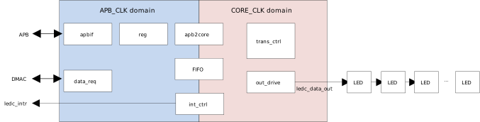
trans_ctrl:配置 LED 时序、数据顺序、数据传输模式、数据长度和 LED 数量
FIFO:32 * 24 位 FIFO,用于发送 LED 数据
Int_ctrl:指示 LED 控制器的 FIFO 状态,包括等待数据超时或数据溢出异常
data_out:根据 trans_ctrl 配置,将输入数据转换为逻辑字符 '0' 和字符 '1'
功能描述
输出时序
逻辑 "1" 码、逻辑 "0" 码和刷新周期的序列因智能 LED 而异。基本序列解码图如图所示。
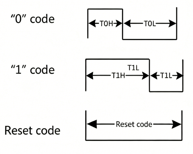
LED 解码数据序列图
为了生成可配置的 LED 序列信号,LEDC 根据 LEDC_LED_T01_TIMING_CTRL_REG 的 LEDC_T1H_CNT / LEDC_T1L_CNT (寄存器 0x004[31:16]) 和 LEDC_T0H_CNT / LEDC_T0L_CNT (寄存器 0x004[15:0]) 对若干个 XTAL40MHz 时钟周期进行计数。LEDC 输出信号如图所示。

IDLE 状态为高电平时的 LEDC 输出数据格式
传输时序
下图展示了 LEDC 的帧输出。在发送一帧数据之前,先发送一个 RESET 以刷新 LED 灯珠。'wait_time1' 用于降低刷新速率,可通过将 LEDC_WAIT_TIME1_CTRL_REG 的 LEDC_BIT_WAIT_TIME1_EN (寄存器 0x014[31]) 设置为 0 来禁用。只有一次扫描的最后一帧可能少于 LED 数量。

LEDC 一次扫描的输出时序图
RESET:一段保持低电平的时间,用于刷新 LED 灯珠。
Pixel:24 位逻辑 '0' 或 '1' 数据被解码为由一个数据包或一个像素组成的波形。LED 灯珠通过内部信号整形放大电路旁路低电平并整形高电平。
wait_time0:两个像素数据之间的一段低电平时间。此项为可选。
wait_time1:除第一帧外,RESET 之后的一段低电平时间。此项为可选。
Frame:LED 灯珠的总数。一帧在 LEDC 向 LED 灯珠发送 RESET 之后开始。
Scan:包含全部数据包。一次扫描可以包含多个帧或少于一个帧。当软件配置 LEDC 并将 LEDC_CTRL_REG 的
LEDC_BIT_EN(寄存器 0x00[0]) 置 1 时,扫描开始。当 LEDC 被禁用时,扫描停止。
LED 级联方式
LEDC 输出的数据模式基于智能 LED 灯珠。LED 灯珠的典型应用电路如图所示。
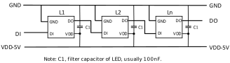
LED 典型应用电路
所支持的 RGB LED 灯珠采用自动整形传输技术。LEDC 按照下图的顺序发送数据,其中 N 代表 LEDC 驱动的 LED 数量,Dn 代表第 N 个 LED 接收到的数据。
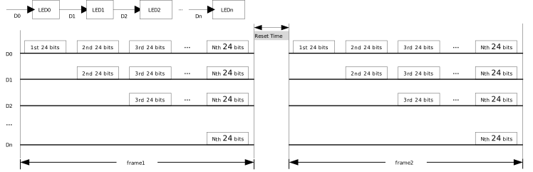
LEDC 数据传输序列
智能 LED 灯珠会从 Din 捕获第一个 24 位数据包,对后续数据进行整形后从 Dout 输出。若要刷新 LED 灯珠的缓冲数据,需要在 DI 输入新数据包之前向该 LED 灯珠发送一个 RESET。
RGB LED 数据结构
对于 LED 灯珠,控制电路和 RGB 芯片集成在一个封装内,形成一个完整的可寻址像素。每个像素的三原色均可实现 256 级亮度显示,可完成 16777216 种颜色的全彩显示。
每个数据输入为 RGB888 格式。LEDC 在输入和输出端口兼容不同的数据模式。默认情况下,24 位数据以 GRB 模式发送,如图所示。高位先传输。

GRB 的 LEDC 数据 MSB 顺序
确定 LEDC 输入和输出数据模式后,软件根据下表设置 LEDC_CTRL_REG 的 LEDC_MASK_LED_RGB_MODE (寄存器 0x00[8:6])。
RGB 输出模式 |
输入 GRB |
输入 GBR |
输入 RGB |
输入 RBG |
输入 BGR |
输入 BRG |
|---|---|---|---|---|---|---|
000 |
GRB |
GBR |
RGB |
RBG |
BGR |
BRG |
001 |
GBR |
GRB |
RBG |
RGB |
BRG |
BGR |
010 |
RGB |
BGR |
GRB |
BRG |
GBR |
RBG |
011 |
BGR |
RGB |
BRG |
GRB |
RBG |
GBR |
100 |
RBG |
BRG |
GBR |
BGR |
GRB |
RGB |
101 |
BRG |
RBG |
BGR |
GBR |
RGB |
GRB |
工作模式
LEDC 数据传输模式支持 DMA 模式和 CPU 中断模式,通过设置 LEDC_DMA_CTRL_REG 的 LEDC_BIT_DMA_EN (寄存器 0x1C[5]) 进行选择。内部 FIFO 深度为 32,数据宽度为 24 位。FIFO 触发阈值通过 LEDC_DMA_CTRL_REG 的 LEDC_FIFO_TRIG_LEVEL (寄存器 0x1C[4:0]) 配置,推荐值为 7 或 15。
DMA 模式
当 LEDC_DMA_CTRL_REG 的 LEDC_BIT_DMA_EN (寄存器 0x1C[5]) 设置为 1 时,LEDC 进入 DMA 模式。在此模式下,LEDC 作为 DMA 传输的流控制器。推荐的突发长度为 8 或 16,最大突发长度为 32。当剩余待传输数据大于或等于突发长度,且内部 FIFO 的有效空间大于 LEDC_FIFO_TRIG_LEVEL 设定的阈值时,LEDC 请求一次 DMA 突发传输。每次 APB 写入数据时,仅低 24 位有效。当剩余待传输数据小于突发长度且内部 FIFO 未满时,LEDC 请求一次 DMA 单次传输。
CPU 中断模式
当 LEDC_DMA_CTRL_REG 的 LEDC_BIT_DMA_EN (寄存器 0x1C[5]) 设置为 0 时,LEDC 进入 CPU 中断模式。当剩余待传输数据大于 0 且内部 FIFO 空闲空间小于 LEDC_FIFO_TRIG_LEVEL 设定的阈值时,LEDC 在 LEDC_LED_INT_STS_REG 中产生 FIFO_CPUREQ_INT 中断。CPU 获取该中断后,可通过 APB 总线将数据从内存传输到 LEDC FIFO。
LEDC 中断
LEDC 共有四种中断:FIFO_OVERFLOW_INT、WAITDATA_TIMEOUT_INT、FIFO_CPUREQ_INT 和 LEDC_TRANS_FINISH_INT。各中断可通过 LEDC_LED_INTERRUPT_CTRL_REG 中对应的中断使能位独立屏蔽,并通过 LEDC_LED_INTERRUPT_CTRL_REG 的 LEDC_BIT_GLOBAL_INT_EN (寄存器 0x020[4]) 全局使能或禁用。当产生 FIFO_OVERFLOW_INT、WAITDATA_TIMEOUT_INT 或 LEDC_TRANS_FINISH_INT 时,LEDC 状态机进入 TRAP 状态,软件应设置 LEDC_CTRL_REG 的 LEDC_BIT_SOFT_RESET (寄存器 0x00[1]) 进行复位。
中断描述
各中断的触发条件和清除方式描述如下:
FIFO 溢出中断(
FIFO_OVERFLOW_INT)——当外部写入的数据超过 LEDC FIFO 的最大存储空间时置位,LEDC 将处于数据丢失状态并进入 TRAP 状态。该中断状态通过设置 LEDC_CTRL_REG 的LEDC_BIT_SOFT_RESET(寄存器 0x00[1]) 清除。在 DMA 模式下,由于 FIFO 阈值设置为所需的 FIFO 深度的 1/4 或 1/2,因此不会发生此情况。LEDC 作为流控制器,会根据 FIFO 阈值发送 dma_req,该阈值与 DMA 源数据宽度和目标数据宽度匹配。而在 CPU 模式下,需注意待发送的数据不超过 FIFO 的剩余空间。等待数据超时中断(
WAITDATA_TIMEOUT_INT)——当已发送数据请求但未及时将数据推送到 LEDC FIFO 时置位。等待数据阶段包括 wait_time0/1 和 wait_data0/1,如下图所示。如果 LEDC 的内部 FIFO 因某些异常情况无法获取数据,LEDC 进入等待数据状态。这可能在两个 24 位数据包之间发生,其中 (Twait_time0 + Twait_data0) >= min(LED_WAIT_DATA_TIME, RESET_TIME);或在两个帧之间发生,其中 Twait_data1 >= LED_WAIT_DATA_TIME。该中断状态通过设置 LEDC_CTRL_REG 的LEDC_BIT_SOFT_RESET(寄存器 0x00[1]) 清除。发生此情况时,请重启 LEDC 并及时发送数据。

传输中 wait_data0 和 wait_data1 状态的位置
FIFO 请求 CPU 数据中断(
FIFO_CPUREQ_INT)——仅在 CPU 模式下使用。当 FIFO 数据可用空间小于 LEDC_DMA_CTRL_REG 的LEDC_FIFO_TRIG_LEVEL(寄存器 0x1C[4:0]) 设定的阈值时置位。CPU 获取该中断后,可通过 APB 总线将数据从内存传输到 LEDC FIFO。该中断状态通过设置 LEDC_CTRL_REG 的LEDC_BIT_SOFT_RESET(寄存器 0x00[1]) 清除。LEDC 传输完成中断(
LEDC_TRANS_FINISH_INT)——当 LEDC 已将所有数据包发送到 LED 灯珠时置位。此时 LEDC_DATA_FINISH_CNT_REG 的LEDC_LED_DATA_FINISH_CNT等于 LEDC_CTRL_REG 中设置的 TOTAL_DATA_LENGTH,硬件将LEDC_BIT_EN(寄存器 0x00[0]) 复位为 0。LEDC 状态机进入 TRAP 状态,然后切换到 IDLE 状态。该中断状态通过设置 LEDC_CTRL_REG 的LEDC_BIT_SOFT_RESET(寄存器 0x00[1]) 清除。
寄存器
Base Address: 0x41105000
Name |
Address offset |
Access |
Description |
|---|---|---|---|
000h |
R/W |
||
004h |
R/W |
||
008h |
R/W |
||
00Ch |
R/W |
||
010h |
R/W |
||
014h |
R/W |
||
018h |
R/W |
||
01Ch |
R/W |
||
020h |
R/W |
||
024h |
R/W |
||
030h |
R/W |
||
0F0h |
R/W |
||
0F4h |
R/W |
REG_LEDC_CTRL_REG
Name: LEDC Control Register
Size: 32
Address offset: 000h
Read/write access: R/W
Bit |
Symbol |
Access |
INI |
Description |
|---|---|---|---|---|
31:29 |
RSVD |
R |
- |
Reserved |
28:16 |
TOTAL_DATA_LENGTH |
R/W |
0x0 |
Total length of transfer data, range from 1 to 8K (unit: 32 bits, only low 24-bit is valid). Actual transfer package is TOTAL_DATA_LENGTH+1. The field is recommended to an integer multiple of (LED_NUM+1). 备注 If TOTAL_DATA_LENGTH is greater than (LED_NUM+1) but not integer multiple, the last frame of data will be transfered less than (LED_NUM+1). |
15:11 |
RSVD |
R |
- |
Reserved |
10 |
RESET_LED_EN |
R/W |
0x0 |
Write operation: When software writes 1 to this bit, LEDC FSM turns to CPU_RESET_LED state, and CPU triggers LEDC to transfer a reset to LED. 备注 Only when LEDC is in IDLE state, FSM can turn to CPU_RESET_LED state.
Read operation:
|
9 |
LED_POLARITY |
R/W |
0x0 |
LED DI level when free.
|
8:6 |
LED_RGB_MODE |
R/W |
0x0 |
LEDC inputs 24 bits data package in order of {byte2, byte1, byte0}.
|
5 |
LED_MSB_TOP |
R/W |
0x1 |
Source RGB data format.
|
4 |
LED_MSB_BYTE2 |
R/W |
0x1 |
LEDC outputs 24 bits data package in order of {byte2, byte1, byte0}.
|
3 |
LED_MSB_BYTE1 |
R/W |
0x1 |
LEDC outputs 24 bits data package in order of {byte2, byte1, byte0}.
|
2 |
LED_MSB_BYTE0 |
R/W |
0x1 |
LEDC outputs 24 bits data package in order of {byte2, byte1, byte0}.
|
1 |
LEDC_SOFT_RESET |
R/W |
0x0 |
LEDC software reset. If software writes 1 to this bit, the next cycle hardware will clear LEDC_SOFT_RESET to 0, which will generate a pulse. LEDC soft reset includes all interrupt status register, the control state machine returns to the IDLE state, LEDC FIFO read and write point is cleared to 0, LEDC interrupt is cleared. The related registers are as below:
Other registers remain unchanged. |
0 |
LEDC_EN |
R/W |
0x0 |
LEDC enable bit.
This bit enable indicates that LEDC can be started when LEDC data has finished transmission, or this bit is cleared to 0 by hardware when software sets LEDC_SOFT_RESET. Software clearing LEDC_EN when LEDC FSM is not IDLE doesn't affect data transfer. |
REG_LED_T01_TIMING_CTRL_REG
Name: LED Timing Control Register
Size: 32
Address offset: 004h
Read/write access: R/W
Bit |
Symbol |
Access |
INI |
Description |
|---|---|---|---|---|
31:24 |
T1H_CNT |
R/W |
0x20 |
LED modulate logical "1" high level time (T1H_TIME). Unit: cycle (40MHz), T1H_TIME = 25ns * T1H_CNT, where T1H_CNT>0 T1H_TIME default value is 800ns. |
23:16 |
T1L_CNT |
R/W |
0xc |
LED modulate logical "1" low level time. Unit: cycle (40MHz), T1L_TIME = 25ns *T1L_CNT, where T1L_CNT>0 T1L_TIME default value is 300ns. |
15:8 |
T0H_CNT |
R/W |
0xc |
LED modulate logical "0" high level time. Unit: cycle (40MHz), T0H_TIME = 25ns * T0H_CNT, where T0H_CNT>0 T0H_TIME default value is 300ns. |
7:0 |
T0L_CNT |
R/W |
0x20 |
LED modulate logical "0" low level time. Unit: cycle (40MHz), T0L_TIME = 25ns *T0L_CNT, where T0L_CNT>0 T0L_TIME default value is 800ns. |
REG_LEDC_DATA_FINISH_CNT_REG
Name: LEDC Data Finish Register
Size: 32
Address offset: 008h
Read/write access: R/W
Bit |
Symbol |
Access |
INI |
Description |
|---|---|---|---|---|
31 |
RSVD |
R |
- |
Reserved |
30:16 |
LED_WAIT_DATA_TIME |
R/W |
0x2edf |
The time that internal FIFO of LEDC is waiting for data. The default value is 300us by default. To avoid to insert LED RESET between two-pixel data, hardware will send WAITDATA_TIMEOUT_INT when wait_time>= min(RESET_TIME, LED_WAIT_DATA_TIME). The adjust range is from 25ns ~ 819us, LED_WAIT_DATA_TIME = 25ns *(N+1) where N is from 0 to 0x7FFF. When the setting time is exceeded, LEDC will send WAITDATA_TIMEOUT_INT interrupt. Under this abnormal situation, software should reset LEDC. |
15:13 |
RSVD |
R |
- |
Reserved |
12:0 |
LED_DATA_FINISH_CNT |
R |
0x0 |
The total LED data have been sent (range: 0 ~ 8K). When LEDC transfer finishes normally, this register is cleared by hardware when generating trans_finish_int. Software knows LED_DATA_FINISH_CNT equal to TOTAL_DATA_LENGTH. When LEDC transfer interrupt abnormally, this register will be cleared to 0 by software by setting LEDC_SOFT_RESET. |
REG_LED_RESET_TIMING_CTRL_REG
Name: LED Reset Timing Control Register
Size: 32
Address offset: 00Ch
Read/write access: R/W
Bit |
Symbol |
Access |
INI |
Description |
|---|---|---|---|---|
31:30 |
RSVD |
R |
- |
Reserved |
29:16 |
RESET_TIME |
R/W |
0x2edf |
Reset time control of LED lamp. The default reset time is 300us. The adjust range is from 25ns to 409.6us. RESET_TIME = 25ns *(N+1) where N is from 0 to 0x3FFF. |
15:10 |
RSVD |
R |
- |
Reserved |
9:0 |
LED_NUM |
R/W |
0x0 |
The number of external LED lamp. Maximum up to 1024. The default value is 0, which indicate that 1 LED lamp is connected. The range is from 0 to 1023. |
REG_LEDC_WAIT_TIME0_CTRL_REG
Name: LED Wait Time 0 Control Register
Size: 32
Address offset: 010h
Read/write access: R/W
Bit |
Symbol |
Access |
INI |
Description |
|---|---|---|---|---|
31:10 |
RSVD |
R |
- |
Reserved |
9 |
WAIT_TIME0_EN |
R/W |
0 |
Wait time0 enable. When setting this bit, the controller automatically inserts waiting time before next LED package data.
|
8:0 |
TOTAL_WAIT_TIME0 |
R/W |
0x1FF |
Waiting time between 2 LED data, and LEDC outputs Low level during waiting time0. The adjust range is from 25ns to 12.5us, WAIT_TIME0 = 25ns*(N+1), where N is from 0 to 0x1FF. |
REG_LEDC_WAIT_TIME1_CTRL_REG
Name: LED Wait Time 1 Control Register
Size: 32
Address offset: 014h
Read/write access: R/W
Bit |
Symbol |
Access |
INI |
Description |
|---|---|---|---|---|
31 |
WAIT_TIME1_EN |
R/W |
0 |
Wait time1 enable. When setting this bit, the controller automatically inserts waiting time before next LED frame data.
|
30:0 |
TOTAL_WAIT_TIME1 |
R/W |
0x1FFFFFF |
Waiting time between 2 frame data, and LEDC outputs Low level during waiting time1. The adjust range is from 25ns to 53s, WAIT_TIME0 = 25ns*(N+1), where N is from 0 to 0x7FFFFFFF. |
REG_LEDC_DATA_REG
Name: LED Data Register
Size: 32
Address offset: 018h
Read/write access: R/W
Bit |
Symbol |
Access |
INI |
Description |
|---|---|---|---|---|
31:24 |
RSVD |
R |
- |
Reserved |
23:0 |
LEDC_DATA |
R/W |
0 |
LEDC display data, the lower 24-bit is valid. Writ this register means push data to LEDC FIFO. Register LEDC_EN toggling from 0 to 1 will clear LEDC FIFO. Thus, only data pushed when LEDC_EN=1 will be send to LED. |
REG_LEDC_DMA_CTRL_REG
Name: LED DMA Control Register
Size: 32
Address offset: 01Ch
Read/write access: R/W
Bit |
Symbol |
Access |
INI |
Description |
|---|---|---|---|---|
31:6 |
RSVD |
R |
- |
Reserved |
5 |
LEDC_DMA_EN |
R/W |
0x1 |
LEDC DMA request enable.
|
4:0 |
LEDC_FIFO_TRIG_LEVEL |
R/W |
0xF |
The remaining space of internal FIFO in LEDC. When the remain space of internal LEDC FIFO is larger than LEDC_FIFO_TRIG_LEVEL, a DMA request or cpu_req_int will generate. 备注 The default value is 15. The adjust range is from 0 to 31, and the recommended configuration is 7 or 15. |
REG_LED_INTERRUPT_CTRL_REG
Name: LED Interrupt Control Register
Size: 32
Address offset: 020h
Read/write access: R/W
Bit |
Symbol |
Access |
INI |
Description |
|---|---|---|---|---|
31:5 |
RSVD |
R |
- |
Reserved |
4 |
GLOBAL_INT_EN |
R/W |
0 |
Global interrupt enable.
|
3 |
FIFO_OVERFLOW_INT_EN |
R/W |
0 |
FIFO overflow interrupt enable. When the data written by software is more than internal FIFO level of LEDC, LEDC is in data loss state.
|
2 |
WAITDATA_TIMEOUT_INT_EN |
R/W |
0 |
The internal FIFO in LEDC can't get data after the LED_WAIT_DATA_TIME, the interrupt will be enable.
|
1 |
FIFO_CPUREQ_INT_EN |
R/W |
0 |
FIFO request CPU data interrupt enable.
|
0 |
LED_TRANS_FINISH_INT_EN |
R/W |
0 |
Data transmission complete interrupt enable.
|
REG_LED_INT_STS_REG
Name: LED FIFO Status Register
Size: 32
Address offset: 024h
Read/write access: R/W
Bit |
Symbol |
Access |
INI |
Description |
|---|---|---|---|---|
31:18 |
RSVD |
R |
- |
Reserved |
17 |
FIFO_EMPTY |
R |
0x1 |
FIFO empty status flag. When LEDC_EN is 0, FIFO_EMPTY equal 1. This flush residual data when LED_NUM is not integer multiples of burst length. |
16 |
FIFO_FULL |
R |
0 |
FIFO full status flag. |
15:4 |
RSVD |
R |
- |
Reserved |
3 |
FIFO_OVERFLOW_INT |
R/W |
0 |
FIFO overflow interrupt Clear 0 when software set LEDC_SOFT_RESET. The data written by external is more than the maximum storage space of LEDC FIFO. At this time, software needs to deal with the abnormal situation. LEDC performs soft_reset operation to refresh all data.
|
2 |
WAITDATA_TIMEOUT_INT |
R/W |
0 |
Before transfer a frame: When the internal FIFO in LEDC can't get data after the LED_WAIT_DATA_TIME, this bit is set. During transfer of a frame (between two pixel of data): to avoid insert LED RESET between two pixel data, hardware will send WAITDATA_TIMEOUT_INT when wait_time>= min(RESET_TIME,LED_WAIT_DATA_TIME). Clear 0 when software sets LEDC_SOFT_RESET. When new data arrives at WAIT_DATA state, LEDC will continue sending data. 备注 Software should note that if the waiting time exceeds the operation of reset time, LEDC may enter refresh state, new data has not been sent.
|
1 |
FIFO_CPUREQ_INT |
R/W |
0 |
When FIFO data available is less than the threshold left, the interrupt is reported to CPU. Clear 0 when software sets LEDC_SOFT_RESET.
备注 When getting FIFO_CPUREQ_INT, CPU writes 1 data to LEDC Buffer. It is inefficiently compared to DMA mode. |
0 |
LED_TRANS_FINISH_INT |
R/W |
0 |
When the data configured as TOTAL_DATA_LENGTH has been transferred complete, this bit is set. Clear 0 when software sets LEDC_SOFT_RESET.
|
REG_LEDC_DEBUG_SEL_REG
Name: LED Debug Select Register
Size: 32
Address offset: 030h
Read/write access: R/W
Bit |
Symbol |
Access |
INI |
Description |
|---|---|---|---|---|
31:9 |
RSVD |
R |
- |
Reserved |
8:7 |
LEDC_DEBUG_SEL_DRIVE |
R/W |
0 |
Drive module debug out select. |
6:3 |
LEDC_DEBUG_SEL_FIFO |
R/W |
0 |
FIFO module debug out select. [6:5]: select debug_data of ledc_txfifo, valid range is 0 or 1. [4:3]: select output data byte when bit[6:5] is 0.
|
2:0 |
LEDC_DEBUG_SEL_TOP |
R/W |
0 |
LEDC top module debug out select. |
REG_DUMMY_F0
Name: Dummy register
Size: 32
Address offset: 0F0h
Read/write access: R/W
Bit |
Symbol |
Access |
INI |
Description |
|---|---|---|---|---|
31:0 |
DUMMY |
R/W |
32'hffffffff |
Dummy register |
REG_DUMMY_F4
Name: Dummy register
Size: 32
Address offset: 0F4h
Read/write access: R/W
Bit |
Symbol |
Access |
INI |
Description |
|---|---|---|---|---|
31:0 |
DUMMY |
R/W |
32'h0 |
Dummy register |
Base Address: 0x41015000
Name |
Address offset |
Access |
Description |
|---|---|---|---|
000h |
R/W |
||
004h |
R/W |
||
008h |
R/W |
||
00Ch |
R/W |
||
010h |
R/W |
||
014h |
R/W |
||
018h |
R/W |
||
01Ch |
R/W |
||
020h |
R/W |
||
024h |
R/W |
||
030h |
R/W |
||
0F0h |
R/W |
||
0F4h |
R/W |
REG_LEDC_CTRL_REG
Name: LEDC Control Register
Size: 32
Address offset: 000h
Read/write access: R/W
Bit |
Symbol |
Access |
INI |
Description |
|---|---|---|---|---|
31:29 |
RSVD |
R |
- |
Reserved |
28:16 |
TOTAL_DATA_LENGTH |
R/W |
0x0 |
Total length of transfer data, range from 1 to 8K (unit: 32 bits, only low 24-bit is valid). Actual transfer package is TOTAL_DATA_LENGTH+1. The field is recommended to an integer multiple of (LED_NUM+1). 备注 If TOTAL_DATA_LENGTH is greater than (LED_NUM+1) but not integer multiple, the last frame of data will be transferred less than (LED_NUM+1). |
15:11 |
RSVD |
R |
- |
Reserved |
10 |
RESET_LED_EN |
R/W |
0x0 |
Write operation: When software writes 1 to this bit, LEDC FSM turns to CPU_RESET_LED state, and CPU triggers LEDC to transfer a reset to LED. 备注 Only when LEDC is in IDLE state, can FSM turn to CPU_RESET_LED state.
Read operation:
|
9 |
LED_POLARITY |
R/W |
0x0 |
LED DI level when free.
|
8:6 |
LED_RGB_MODE |
R/W |
0x0 |
LEDC inputs 24 bits data package in order of {byte2, byte1, byte0}.
|
5 |
LED_MSB_TOP |
R/W |
0x1 |
Source RGB data format.
|
4 |
LED_MSB_BYTE2 |
R/W |
0x1 |
LEDC outputs 24 bits data package in order of {byte2, byte1, byte0};
|
3 |
LED_MSB_BYTE1 |
R/W |
0x1 |
LEDC outputs 24 bits data package in order of {byte2, byte1, byte0};
|
2 |
LED_MSB_BYTE0 |
R/W |
0x1 |
LEDC outputs 24 bits data package in order of {byte2, byte1, byte0};
|
1 |
LEDC_SOFT_RESET |
R/W |
0x0 |
LEDC software reset. If software writes 1 to this bit, the next cycle hardware will clear LEDC_SOFT_RESET to 0, which will generate a pulse. LEDC soft reset includes all interrupt status register, the control state machine returns to the IDLE state, LEDC FIFO read and write point is cleared to 0, LEDC interrupt is cleared. The related registers are as below:
Other registers remain unchanged. |
0 |
LEDC_EN |
R/W |
0x0 |
LEDC enable bit.
This bit enable indicates that LEDC can be started when LEDC data has finished transmission, or this bit is cleared to 0 by hardware when software sets LEDC_SOFT_RESET. Software clearing LEDC_EN when LEDC FSM is not IDLE don't affect data transfer. |
REG_LED_T01_TIMING_CTRL_REG
Name: LED Timing Control Register
Size: 32
Address offset: 004h
Read/write access: R/W
Bit |
Symbol |
Access |
INI |
Description |
|---|---|---|---|---|
31:24 |
T1H_CNT |
R/W |
0x20 |
LED modulate logical "1" high level time (T1H_TIME). Unit: cycle (40MHz), T1H_TIME = 25ns * T1H_CNT, where T1H_CNT>0 T1H_TIME default value is 800ns. |
23:16 |
T1L_CNT |
R/W |
0xc |
LED modulate logical "1" low level time. Unit: cycle (40MHz), T1L_TIME = 25ns *T1L_CNT, where T1L_CNT>0 T1L_TIME default value is 300ns. |
15:8 |
T0H_CNT |
R/W |
0xc |
LED modulate logical "0" high level time. Unit: cycle (40MHz), T0H_TIME = 25ns * T0H_CNT, where T0H_CNT>0 T0H_TIME default value is 300ns. |
7:0 |
T0L_CNT |
R/W |
0x20 |
LED modulate logical "0" low level time. Unit: cycle (40MHz), T0L_TIME = 25ns *T0L_CNT, where T0L_CNT>0 T0L_TIME default value is 800ns. |
REG_LEDC_DATA_FINISH_CNT_REG
Name: LEDC Data Finish Register
Size: 32
Address offset: 008h
Read/write access: R/W
Bit |
Symbol |
Access |
INI |
Description |
|---|---|---|---|---|
31 |
RSVD |
R |
- |
Reserved |
30:16 |
LED_WAIT_DATA_TIME |
R/W |
0x2edf |
The time that internal FIFO of LEDC is waiting for data. The default value is 300us by default. To avoid to insert LED RESET between two-pixel data, hardware will send WAITDATA_TIMEOUT_INT when wait_time>= min (RESET_TIME, LED_WAIT_DATA_TIME). The adjust range is from 25ns ~ 819us, LED_WAIT_DATA_TIME = 25ns *(N+1) where N is from 0 to 0x7FFF. When the setting time is exceeded, LEDC will send WAITDATA_TIMEOUT_INT interrupt. Under this abnormal situation, software should reset LEDC. |
15:13 |
RSVD |
R |
- |
Reserved |
12:0 |
LED_DATA_FINISH_CNT |
R |
0x0 |
The total LED data have been sent. (range: 0 ~ 8K). When LEDC transfer finishes normally, this register is cleared by hardware when generating trans_finish_int. Software knows LED_DATA_FINISH_CNT equal to TOTAL_DATA_LENGTH. When LEDC transfers interrupt abnormally, this register will be cleared to 0 by software by setting LEDC_SOFT_RESET. |
REG_LED_RESET_TIMING_CTRL_REG
Name: LED Reset Timing Control Register
Size: 32
Address offset: 00Ch
Read/write access: R/W
Bit |
Symbol |
Access |
INI |
Description |
|---|---|---|---|---|
31:30 |
RSVD |
R |
- |
Reserved |
29:16 |
RESET_TIME |
R/W |
0x2edf |
Reset time control of LED lamp. The default reset time is 300us. The adjust range is from 25ns to 409.6us. RESET_TIME = 25ns *(N+1) where N is from 0 to 0x3FFF. |
15:10 |
RSVD |
R |
- |
Reserved |
9:0 |
LED_NUM |
R/W |
0x0 |
The number of external LED lamp. Maximum up to 1024. The default value is 0, which indicate that 1 LED lamp is connected. The range is from 0 to 1023. |
REG_LEDC_WAIT_TIME0_CTRL_REG
Name: LED Wait Time 0 Control Register
Size: 32
Address offset: 010h
Read/write access: R/W
Bit |
Symbol |
Access |
INI |
Description |
|---|---|---|---|---|
31:10 |
RSVD |
R |
- |
Reserved |
9 |
WAIT_TIME0_EN |
R/W |
0 |
Wait time0 enable. When set this bit, the controller automatically inserts waiting time before next LED package data.
|
8:0 |
TOTAL_WAIT_TIME0 |
R/W |
0x1FF |
Waiting time between 2 LED data, and LEDC outputs Low level during waiting time0. The adjust range is from 25ns to 12.5us, WAIT_TIME0 = 25ns *(N+1) where N is from 0 to 0x1FF. |
REG_LEDC_WAIT_TIME1_CTRL_REG
Name: LED Wait Time 1 Control Register
Size: 32
Address offset: 014h
Read/write access: R/W
Bit |
Symbol |
Access |
INI |
Description |
|---|---|---|---|---|
31 |
WAIT_TIME1_EN |
R/W |
0 |
Wait time1 enable. When set this bit, the controller automatically inserts waiting time before next LED frame data.
|
30:0 |
TOTAL_WAIT_TIME1 |
R/W |
0x1FFFFFF |
Waiting time between 2 frame data, and LEDC outputs Low level during waiting time1. The adjust range is from 25ns to 53s, WAIT_TIME0 = 25ns *(N+1) where N is from 0 to 0x7FFFFFFF. |
REG_LEDC_DATA_REG
Name: LED Data Register
Size: 32
Address offset: 018h
Read/write access: R/W
Bit |
Symbol |
Access |
INI |
Description |
|---|---|---|---|---|
31:24 |
RSVD |
R |
- |
Reserved |
23:0 |
LEDC_DATA |
R/W |
0 |
LEDC display data, the lower 24-bit is valid. Writ this register means push data to LEDC FIFO. Register LEDC_EN toggles from 0 to 1 will clear LEDC FIFO. Thus, only data pushed when LEDC_EN=1 will be send to LED. |
REG_LEDC_DMA_CTRL_REG
Name: LED DMA Control Register
Size: 32
Address offset: 01Ch
Read/write access: R/W
Bit |
Symbol |
Access |
INI |
Description |
|---|---|---|---|---|
31:6 |
RSVD |
R |
- |
Reserved |
5 |
LEDC_DMA_EN |
R/W |
0x1 |
LEDC DMA request enable.
|
4:0 |
LEDC_FIFO_TRIG_LEVEL |
R/W |
0xF |
The remaining space of internal FIFO in LEDC. When the remain space of internal LEDC FIFO is larger than LEDC_FIFO_TRIG_LEVEL, a DMA request or cpu_req_int will generate. 备注 The default value is 15. The adjust range is from 0 to 31, and the recommended configuration is 7 or 15. |
REG_LED_INTERRUPT_CTRL_REG
Name: LED Interrupt Control Register
Size: 32
Address offset: 020h
Read/write access: R/W
Bit |
Symbol |
Access |
INI |
Description |
|---|---|---|---|---|
31:5 |
RSVD |
R |
- |
Reserved |
4 |
GLOBAL_INT_EN |
R/W |
0 |
Global interrupt enable.
|
3 |
FIFO_OVERFLOW_INT_EN |
R/W |
0 |
FIFO overflow interrupt enable. When the data written by software is more than internal FIFO level of LEDC, LEDC is in data loss state.
|
2 |
WAITDATA_TIMEOUT_INT_EN |
R/W |
0 |
The internal FIFO in LEDC can't get data after the LED_WAIT_DATA_TIME, the interrupt will be enable.
|
1 |
FIFO_CPUREQ_INT_EN |
R/W |
0 |
FIFO request CPU data interrupt enable.
|
0 |
LED_TRANS_FINISH_INT_EN |
R/W |
0 |
Data transmission complete interrupt enable.
|
REG_LED_INT_STS_REG
Name: LED Interrupt Status Register
Size: 32
Address offset: 024h
Read/write access: R/W
Bit |
Symbol |
Access |
INI |
Description |
|---|---|---|---|---|
31:18 |
RSVD |
R |
- |
Reserved |
17 |
FIFO_EMPTY |
R |
0x1 |
FIFO empty status flag. When LEDC_EN is 0, FIFO_EMPTY equal 1. This flush residual data when LED_NUM is not integer multiples of burst length. |
16 |
FIFO_FULL |
R |
0 |
FIFO full status flag. |
15:4 |
RSVD |
R |
- |
Reserved |
3 |
FIFO_OVERFLOW_INT |
R/W |
0 |
FIFO overflow interrupt Clear 0 when software set LEDC_SOFT_RESET. The data written by external is more than the maximum storage space of LEDC FIFO. At this time, software needs to deal with the abnormal situation. LEDC performs soft_reset operation to refresh all data.
|
2 |
WAITDATA_TIMEOUT_INT |
R/W |
0 |
Before transfer a frame: When the internal FIFO in LEDC can't get data after the LED_WAIT_DATA_TIME, this bit is set. During transfer of a frame (between two pixel of data): to avoid insert LED RESET between two pixel data, hardware will send WAITDATA_TIMEOUT_INT when wait_time>= min(RESET_TIME,LED_WAIT_DATA_TIME). Clear 0 when software sets LEDC_SOFT_RESET. When new data arrives at WAIT_DATA state, LEDC will continue sending data. 备注 Software should note that if the waiting time exceeds the operation of reset time, LEDC may enter refresh state, new data has not been sent.
|
1 |
FIFO_CPUREQ_INT |
R/W |
0 |
When FIFO data available is less than the threshold left, the interrupt is reported to CPU. Clear 0 when software sets LEDC_SOFT_RESET.
备注 When getting FIFO_CPUREQ_INT, CPU writes 1 data to LEDC Buffer. It is inefficiently compared to DMA mode. |
0 |
LED_TRANS_FINISH_INT |
R/W |
0 |
When the data configured as TOTAL_DATA_LENGTH has been transferred complete, this bit is set. Clear 0 when software sets LEDC_SOFT_RESET.
|
REG_LEDC_DEBUG_SEL_REG
Name: LED Debug Selection Register
Size: 32
Address offset: 030h
Read/write access: R/W
Bit |
Symbol |
Access |
INI |
Description |
|---|---|---|---|---|
31:9 |
RSVD |
R |
- |
Reserved |
8:7 |
LEDC_DEBUG_SEL_DRIVE |
R/W |
0 |
Drive module debug out selection. |
6:3 |
LEDC_DEBUG_SEL_FIFO |
R/W |
0 |
FIFO module debug out select. [6:5]: select debug_data of ledc_txfifo, valid range is 0 or 1 [4:3]: select output data byte when [6:5] is 0.
|
2:0 |
LEDC_DEBUG_SEL_TOP |
R/W |
0 |
LEDC top module debug out select. |
REG_DUMMY_F0
Name: Dummy Register
Size: 32
Address offset: 0F0h
Read/write access: R/W
Bit |
Symbol |
Access |
INI |
Description |
|---|---|---|---|---|
31:0 |
DUMMY |
R/W |
32'hffffffff |
REG_DUMMY_F4
Name: Dummy Register
Size: 32
Address offset: 0F4h
Read/write access: R/W
Bit |
Symbol |
Access |
INI |
Description |
|---|---|---|---|---|
31:0 |
DUMMY |
R/W |
32'h0 |
REGISTER_CONTENTS=RTL8720E
REGISTER_CONTENTS=RTL8720E
REGISTER_CONTENTS=RTL8720E
Base Address: 0x41008000
Name |
Address offset |
Access |
Description |
|---|---|---|---|
000h |
R/W |
||
004h |
R/W |
||
008h |
R/W |
||
00Ch |
R/W |
||
010h |
R/W |
||
014h |
R/W |
||
018h |
R/W |
||
01Ch |
R/W |
||
020h |
R/W |
||
024h |
R/W |
||
030h |
R/W |
REG_LEDC_CTRL_REG
Size: 32
Address offset: 000h
Read/write access: R/W
Bit |
Symbol |
Access |
INI |
Description |
|---|---|---|---|---|
31:29 |
RSVD |
R |
- |
Reserved |
28:16 |
TOTAL_DATA_LENGTH |
R/W |
0x0 |
Total length of transfer data, range from 1 to 8K (unit:32 bits, only low 24-bit is valid). Actual transfer packages is TOTAL_DATA_LENGTH+1. The field is recommended to an integer multiple of (LED_NUM+1). 备注 If TOTAL_DATA_LENGTH is greater than (LED_NUM+1) but not integer multiple, the last frame of data will transfer data less than (LED_NUM+1). |
15:11 |
RSVD |
R |
- |
Reserved |
10 |
RESET_LED_EN |
R/W |
0x0 |
Write operation: When software writes 1 to this bit, LEDC FSM turns to CPU_RESET_LED state, and CPU triggers LEDC to transfer a reset to LED. 备注 Only when LEDC is in the IDLE state, can FSM turn to CPU_RESET_LED state.
Read operation:
|
9 |
LED_POLARITY |
R/W |
0x0 |
LED DI level when free.
|
8:6 |
LED_RGB_MODE |
R/W |
0x0 |
LEDC inputs 24 bits data pakage in order of {byte2, byte1, byte0}.
|
5 |
LED_MSB_TOP |
R/W |
0x1 |
Source RGB data format.
|
4 |
LED_MSB_BYTE2 |
R/W |
0x1 |
LEDC outputs 24 bits data pakage in order of {byte2, byte1, byte0};
|
3 |
LED_MSB_BYTE1 |
R/W |
0x1 |
LEDC outputs 24 bits data pakage in order of {byte2, byte1, byte0};
|
2 |
LED_MSB_BYTE0 |
R/W |
0x1 |
LEDC outputs 24 bits data pakage in order of {byte2, byte1, byte0};
|
1 |
LEDC_SOFT_RESET |
R/W |
0x0 |
LEDC software reset. If software writes 1 to LEDC_SOFT_RESET, the next cycle hardware will clear LEDC_SOFT_RESET to 0, which will generate a pulse. LEDC soft reset includes all interrupt status register, the control state machine returns to the IDLE state, LEDC FIFO read and write point is cleared to 0, LEDC interrupt is cleared. The related registers are as below:
Other registers remain unchanged. |
0 |
LEDC_EN |
R/W |
0x0 |
LEDC enable bit.
This bit enable indicates that LEDC can be started when LEDC data finished transmission, or this bit is cleared to 0 by hardware when software sets LEDC_SOFT_RESET. Software clears LEDC_EN when LEDC FSM is not IDLE don't affect data transfer. |
REG_LED_T01_TIMING_CTRL_REG
Size: 32
Address offset: 004h
Read/write access: R/W
Bit |
Symbol |
Access |
INI |
Description |
|---|---|---|---|---|
31:24 |
T1H_CNT |
R/W |
0x20 |
LED modulate logical "1" high level time (T1H_TIME). Unit: cycle (40MHz), T1H_TIME = 25ns * T1H_CNT , where T1H_CNT>0 T1H_TIME default value is 800ns. |
23:16 |
T1L_CNT |
R/W |
0xc |
LED modulate logical "1" low level time. Unit: cycle (40MHz), T1L_TIME = 25ns *T1L_CNT, where T1L_CNT>0 T1L_TIME default value is 300ns. |
15:8 |
T0H_CNT |
R/W |
0xc |
LED modulate logical "0" hgh level time. Unit: cycle (40MHz), T0H_TIME = 25ns * T0H_CNT , where T0H_CNT>0 T0H_TIME default value is 300ns. |
7:0 |
T0L_CNT |
R/W |
0x20 |
LED modulate logical "0" low level time. Unit: cycle (40MHz), T0L_TIME = 25ns *T0L_CNT, where T0L_CNT>0 T0L_TIME default value is 800ns. |
REG_LEDC_DATA_FINISH_CNT_REG
Size: 32
Address offset: 008h
Read/write access: R/W
Bit |
Symbol |
Access |
INI |
Description |
|---|---|---|---|---|
31 |
RSVD |
R |
- |
Reserved |
30:16 |
LED_WAIT_DATA_TIME |
R/W |
0x2edf |
The time that internal FIFO of LEDC is waiting for data. The default value is 300us by default. To avoid insert LED RESET between two pixel data, hardware will send WAITDATA_TIMEOUT_INT when wait_time>= min (RESET_TIME, LED_WAIT_DATA_TIME). The adjust range is from 25ns ~ 819us, LED_WAIT_DATA_TIME = 25ns *(N+1) where N is from 0 to 0x7FFF. When the setting time is exceeded, LEDC will send WAITDATA_TIMEOUT_INT interrupt. Under this abnormal situation, software should reset LEDC. |
15:13 |
RSVD |
R |
- |
Reserved |
12:0 |
LED_DATA_FINISH_CNT |
R |
0x0 |
The total LED data have been sent. (range: 0 ~ 8K). When LEDC transfer finishs normally, this register is cleared by hardware when generate trans_finish_int. Software knows LED_DATA_FINISH_CNTequals to TOTAL_DATA_LENGTH. When LEDC transfer interrupt abnormally,this register will clear to 0 by software by setting LEDC_SOFT_RESET. |
REG_LED_RESET_TIMING_CTRL_REG
Size: 32
Address offset: 00Ch
Read/write access: R/W
Bit |
Symbol |
Access |
INI |
Description |
|---|---|---|---|---|
31:30 |
RSVD |
R |
- |
Reserved |
29:16 |
RESET_TIME |
R/W |
0x2edf |
Reset time control of LED lamp. The default reset time is 300us. The adjust range is from 25ns to 409.6us. RESET_TIME = 25ns *(N+1) where N is from 0 to 0x3FFF. |
15:10 |
RSVD |
R |
- |
Reserved |
9:0 |
LED_NUM |
R/W |
0x0 |
The number of external LED lamp. Maximum up to 1024. The default value is 0, which indicate that 1 LED lamp is connected. The range is from 0 to 1023. |
REG_LEDC_WAIT_TIME0_CTRL_REG
Size: 32
Address offset: 010h
Read/write access: R/W
Bit |
Symbol |
Access |
INI |
Description |
|---|---|---|---|---|
31:10 |
RSVD |
R |
- |
Reserved |
9 |
WAIT_TIME0_EN |
R/W |
0 |
Wait time0 enable. When set this bit, the controller automatically insert waiting time before next LED package data.
|
8:0 |
TOTAL_WAIT_TIME0 |
R/W |
0x1FF |
Waiting time between 2 LED data, and LEDC output Low level during waiting time0. The adjust range is from 25ns to 12.5us, WAIT_TIME0 = 25ns *(N+1) where N is from 0 to 0x1FF. |
REG_LEDC_WAIT_TIME1_CTRL_REG
Size: 32
Address offset: 014h
Read/write access: R/W
Bit |
Symbol |
Access |
INI |
Description |
|---|---|---|---|---|
31 |
WAIT_TIME1_EN |
R/W |
0 |
Wait time1 enable. When set this bit, the controller automatically insert waiting time before next LED frame data.
|
30:0 |
TOTAL_WAIT_TIME1 |
R/W |
0x1FFFFFF |
Waiting time between 2 frame data, and LEDC output Low level during waiting time1. The adjust range is from 25ns to 53s, WAIT_TIME0 = 25ns *(N+1) where N is from 0 to 0x7FFFFFFF. |
REG_LEDC_DATA_REG
Size: 32
Address offset: 018h
Read/write access: R/W
Bit |
Symbol |
Access |
INI |
Description |
|---|---|---|---|---|
31:24 |
RSVD |
R |
- |
Reserved |
23:0 |
LEDC_DATA |
R/W |
0 |
LEDC display data, the lower 24-bit is valid. Write this register means push data to LEDC FIFO. Register LEDC_EN toggle from 0->1 will clear LEDC FIFO. Thus, only data pushed when LEDC_EN=1 will be send to LED. |
REG_LEDC_DMA_CTRL_REG
Size: 32
Address offset: 01Ch
Read/write access: R/W
Bit |
Symbol |
Access |
INI |
Description |
|---|---|---|---|---|
31:6 |
RSVD |
R |
- |
Reserved |
5 |
LEDC_DMA_EN |
R/W |
0x1 |
LEDC DMA request enable.
|
4:0 |
LEDC_FIFO_TRIG_LEVEL |
R/W |
0xF |
The remaining space of internal FIFO in LEDC When the remain space of internal LEDC FIFO is larger than LEDC_FIFO_TRIG_LEVEL,will generate dma request or cpu_req_int. 备注 : The default value is 15. The adjust range is from 0 to 31, and the recommended cofiguration is 7 or 15. |
REG_LED_INTERRUPT_CTRL_REG
Size: 32
Address offset: 020h
Read/write access: R/W
Bit |
Symbol |
Access |
INI |
Description |
|---|---|---|---|---|
31:5 |
RSVD |
R |
- |
Reserved |
4 |
GLOBAL_INT_EN |
R/W |
0 |
Global interrupt enable.
|
3 |
FIFO_OVERFLOW_INT_EN |
R/W |
0 |
FIFO overflow interrupt enable. When the data wriiten by software is more than internal FIFO level of LEDC, LEDC is in data loss state.
|
2 |
WAITDATA_TIMEOUT_INT_EN |
R/W |
0 |
The internal FIFO in LEDC can`t get data after the LED_WAIT_DATA_TIME, the interrupt will be enable.
|
1 |
FIFO_CPUREQ_INT_EN |
R/W |
0 |
FIFO request CPU data interrupt enable.
|
0 |
LED_TRANS_FINISH_INT_EN |
R/W |
0 |
Data transmission complete interrupt enable.
|
REG_LED_INT_STS_REG
Size: 32
Address offset: 024h
Read/write access: R/W
Bit |
Symbol |
Access |
INI |
Description |
|---|---|---|---|---|
31:18 |
RSVD |
R |
- |
Reserved |
17 |
FIFO_EMPTY |
R |
0x1 |
FIFO empty status flag. When LEDC_EN is 0, FIFO_EMPTY equal 1. This flush residual data when LED_NUM is not integer multiples of burst length. |
16 |
FIFO_FULL |
R |
0 |
FIFO full status flag. |
15:4 |
RSVD |
R |
- |
Reserved |
3 |
FIFO_OVERFLOW_INT |
R/W |
0 |
FIFO overflow interrupt Clear 0 when software set LEDC_SOFT_RESET. The data written by external is more than the maximum storage space of LEDC FIFO. At this time, software needs to deal with the abnormal situation.LEDC performs soft_reset operation to refresh all data.
|
2 |
WAITDATA_TIMEOUT_INT |
R/W |
0 |
Before transfer a frame: When the internal FIFO in LEDC can`t get data after the LED_WAIT_DATA_TIME,this bit is set. During transfer of a frame (between two pixel of data): To avoid insert LED RESET between two pixel data, hardware will send WAITDATA_TIMEOUT_INT when wait_time>= min(RESET_TIME,LED_WAIT_DATA_TIME). Clear 0 when software set LEDC_SOFT_RESET. When new data arrives at WAIT_DATA state, LEDC will continue sending data. 备注 : software should notice if the waiting time exceeds the operation of reset time, LEDC may enter refresh state, new data has not been sent.
|
1 |
FIFO_CPUREQ_INT |
R/W |
0 |
When FIFO data available is less than the threshold left, the interrupt is reported to CPU. Clear 0 when software set LEDC_SOFT_RESET.
备注 when get FIFO_CPUREQ_INT, CPU write 1 data to LEDC Buffer. It is inefficiently compares to DMA mode. |
0 |
LED_TRANS_FINISH_INT |
R/W |
0 |
When the data configured as TOTAL_DATA_LENGTH has been transferred complete, this bit is set. Clear 0 when software set LEDC_SOFT_RESET.
|
REG_LEDC_DEBUG_SEL_REG
Size: 32
Address offset: 030h
Read/write access: R/W
Bit |
Symbol |
Access |
INI |
Description |
|---|---|---|---|---|
31:9 |
RSVD |
R |
- |
Reserved |
8:7 |
LEDC_DEBUG_SEL_DRIVE |
R/W |
0 |
Drive module debug out select. |
6:3 |
LEDC_DEBUG_SEL_FIFO |
R/W |
0 |
Fifo module debug out select. [6:5] select debug_data of ledc_txfifo, valid range 0,1 [4:3] select output data byte when [6:5] is 0.
|
2:0 |
LEDC_DEBUG_SEL_TOP |
R/W |
0 |
Ledc top module debug out select. |