通用输入输出 (GPIO)
简介
GPIO 模块是一个可编程外设,可灵活控制外部 I/O pad 信号。
芯片集成了多个独立的 GPIO 控制器,按 Port A、Port B 等方式组织。每个端口支持以下主要的逐引脚功能:通过存储器映射寄存器实现方向控制(输入或输出)、输出数据控制和输入状态回读,以及用于事件驱动系统响应的外部中断检测。在每个端口内,每个引脚独立运行,允许对 I/O 信号进行细粒度的配置和监控。
每个端口包含多组寄存器,包括基本 I/O 控制寄存器(GPIO_DR、GPIO_DDR、GPIO_EXT_PORT)、中断控制寄存器(GPIO_INT_XXX)和消抖控制寄存器(GPIO_DB_DIV_CONFIG)。消抖功能按组级别进行控制,而所有其他寄存器提供位级别的控制,每个位对应一个独立的 GPIO 引脚。
特性
最多 64 个引脚
Port A: PA0 ~ PA31
Port B: PB0 ~ PB31
最多 52 个引脚
Port A: PA0 ~ PA31
Port B: PB0 ~ PB19
最多 52 个引脚
Port A: PA0 ~ PA31
Port B: PB0 ~ PB19
最多 52 个引脚
Port A: PA0 ~ PA31
Port B: PB0 ~ PB19
最多 52 个引脚
Port A: PA0 ~ PA31
Port B: PB0 ~ PB19
最多 96 个引脚
Port A: PA0 ~ PA31
Port B: PB0 ~ PB31
Port C: PC0 ~ PC31
最多 94 个引脚
Port A: PA0 ~ PA31
Port B: PB0 ~ PB31
Port C: PC0 ~ PC29
输出竞态条件保护
最多 37 个引脚
Port A: PA0 ~ PA31
Port B: PB0 ~ PB4
输出竞态条件保护
独立的寄存器控制
每个 GPIO 信号拥有独立的数据寄存器和数据方向寄存器
灵活的中断模式
可选择的电平触发中断检测
可选择的边沿触发中断检测
消抖功能
使用慢速时钟源的可配置消抖电路
对中断引脚进行有效的噪声过滤
框图
GPIO 的框图如下所示。
GPIO 模块由以下主要功能接口组组成:
APB 接口:连接到 APB 桥,用于内存映射寄存器访问,使软件能够配置和控制 GPIO 功能。
外部数据接口:直接与物理 I/O pad 连接,用于驱动输出信号或从外部引脚采样输入数据。
中断接口:当配置的 GPIO 事件发生时,向系统中断控制器发送中断请求,并接收中断确认信号。
功能描述
本节描述 GPIO 的功能。
方向控制
每个 I/O 信号的方向通过对应的 Port X 数据方向寄存器 (GPIO_DDR) 进行配置。 GPIO_DDR 中的每一位独立控制其对应信号的方向(输入或输出)。处理器可通过 APB 总线接口访问 GPIO_DDR 寄存器。
数据和控制流的架构如以下框图所示。
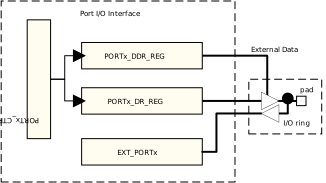
在 GPIO_DDR 中,每一位均可单独控制,因此该寄存器实际上为宽度为 N 的 Port X GPIO 总线提供了 N 个独立的方向控制位(位索引范围为 0 到 N-1)。
对于 GPIO_DDR 中的每一位:
写入
1将对应的 I/O 信号配置为输出。写入
0将对应的 I/O 信号配置为输入。
数据输出
当 GPIO 引脚被配置为输出时,写入 Port X 数据寄存器 (GPIO_DR) 的数据会按位直接驱动对应 I/O 信号的输出缓冲器。
GPIO_DR 中的每一位控制一个输出信号:
写入
1将对应的 I/O 信号输出驱动为高电平。写入
0将对应的 I/O 信号输出驱动为低电平。
竞态条件保护
不支持。
不支持。
不支持。
不支持。
不支持。
不支持。
GPIO 按端口组织,每个端口通常包含多个 GPIO 引脚,这些引脚共享一个输出值寄存器。由于单个引脚的输出状态无法被原子性地修改,因此更新单个 GPIO 输出需要执行读-改-写(read-modify-write)操作序列。这在多任务或多线程环境中会引入潜在的竞态条件,并发访问同一端口可能导致引脚状态异常。
为解决此问题,芯片实现了由寄存器位 0x4080A2C4[31] 控制的硬件级竞态条件保护。当该位 未置位 时,输出由 GPIO_DR 在 普通输出模式 中直接控制。当该位 置位 时,控制逻辑的行为如下:
写入
1翻转位值并反转 I/O 信号输出。写入
0保持位值不变,维持 I/O 信号输出。
GPIO 按端口组织,每个端口通常包含多个 GPIO 引脚,这些引脚共享一个输出值寄存器。由于单个引脚的输出状态无法被原子性地修改,因此更新单个 GPIO 输出需要执行读-改-写(read-modify-write)操作序列。这在多任务或多线程环境中会引入潜在的竞态条件,并发访问同一端口可能导致引脚状态异常。
为解决此问题,芯片实现了由寄存器位 0x408012C4[31] 控制的硬件级竞态条件保护。当该位 未置位 时,输出由 GPIO_DR 在 普通输出模式 中直接控制。当该位 置位 时,控制逻辑的行为如下:
写入
1翻转位值并反转 I/O 信号输出。写入
0保持位值不变,维持 I/O 信号输出。
数据输入
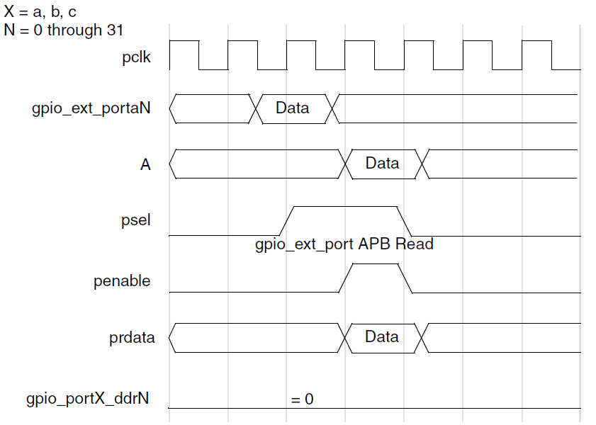
通过 APB 总线读取 GPIO_EXT_PORT 寄存器可获取外部引脚的电平状态。无论引脚配置为输入或输出模式,该寄存器的读回值均为外部引脚实际电平对应的逻辑值。
备注
当 GPIO 配置为输出模式且 GPIO_DR 输出高电平(逻辑值 1)时,若外部引脚连接至低电平(如 GND),读取 GPIO_EXT_PORT 将返回 0,表明外部引脚实际处于低电平状态。
GPIO_EXT_PORT 寄存器是只读的,意味着无法通过 APB 软件接口对其进行写操作。
下图展示了当方向设置为输入且包含亚稳态寄存器时,读取 GPIO_EXT_PORT 内存映射寄存器的时序图,亚稳态寄存器会引入端口线的数据延迟。
备注
从 GPIO_EXT_PORT 连续读取时能够读回的最大数据速率必须小于 PCLK/2 。由于 APB 的非流水线特性,每次读访问需要两个 pclk 周期。前提假设是当 PCLK=HCLK 时,APB 桥在连续访问期间不会失去 AHB 的所有权。
中断
GPIO 外设支持在任何 GPIO 引脚上配置可编程的中断源,中断类型可通过以下设置进行编程:
边沿触发中断:上升沿、下降沿或双边沿
电平触发中断:高电平有效或低电平有效
中断屏蔽通过 GPIO_INT_MASK 寄存器实现,同时提供屏蔽后(GPIO_INT_STATUS)和原始(GPIO_INT_STATUS_RAW)的中断状态信息。配置中断需要将 GPIO 端口的数据方向设置为 Input(输入)。将方向重新编程为 Output(输出)时,待处理的中断会保留,但不会产生新的中断。
下图展示了中断生成和数据流,包含两种可能的输出架构:
独立中断模式:独立的信号(gpio_intr[N] 或 gpio_intr_n[N])
组合中断模式:单一统一信号(gpio_intr_flag 或 gpio_intr_flag_n)
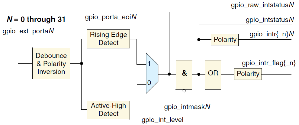
中断 RTL 框图
在组合模式下,中断信号通过对所有独立中断线进行逻辑 OR 运算生成。本芯片采用组合中断架构。每个 GPIO 端口在系统中断控制器中拥有一个专用的 IRQ 编号。由于采用组合中断实现方式,ISR 必须读取 GPIO_INT_STATUS 寄存器以确定是哪些 GPIO 引脚触发了中断。处理器通过软件负责中断优先级排序和处理。
中断同步
中断信号可以在内部同步到专用系统时钟 pclk_intr,同步要求由中断类型决定:
边沿触发中断:必须同步到 pclk_intr。送到处理器的边沿触发中断信号保证与系统总线时钟同步。
电平触发中断:同步到 pclk_intr 是可选的,可通过软件配置 GPIO_INT_LS_SYNC 寄存器来控制。
pclk_intr 信号在电源管理系统中起着关键作用。如果系统要求在 GPIO pclk 被关闭时仍具备中断检测能力,则必须提供 pclk_intr。通常假设 pclk_intr 与 pclk 同步运行。反之,如果仅在 pclk 运行时才需要检测中断,则可以将 pclk_intr 和 pclk 连接到同一个时钟源。
边沿触发中断
边沿触发中断通过向 GPIO_INT_EOI 寄存器写入来清除,该操作会同时清除中断状态寄存器和原始状态寄存器。建议在向 GPIO_INT_EOI 写入之前先清除中断源。此寄存器对电平触发中断无效。在组合中断配置中,可以同时清除多个边沿触发中断。
单边沿检测
下图展示了当 GPIO_INT_BOTH_EDGE = 0 时,gpio_ext_portaN 信号上的中断源同步与边沿检测的 RTL 示意图。
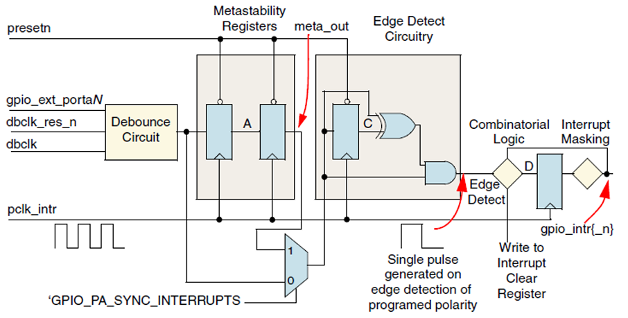
同步与边沿检测中断生成 (GPIO_INT_BOTH_EDGE=0)
备注
亚稳态部分默认包含在内。
图 GPIO 中断亚稳态 展示了一个在 Port A 输入上升沿产生中断的时序图;在该场景中,消抖逻辑被禁用,亚稳态寄存器被包含在内。该图还展示了通过写入中断清除寄存器来清除中断的方式。
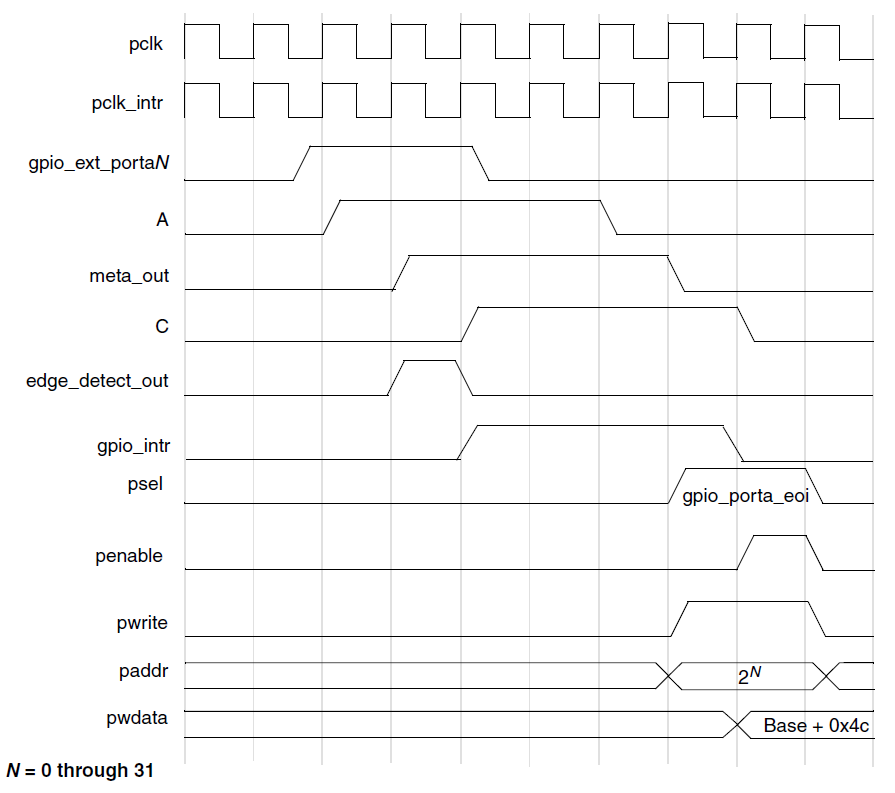
中断边沿检测与中断清除时序 (GPIO_SYNC_PA_INTERRUPTS = 1,包含亚稳态寄存器)
可能会出现以下情况:中断服务程序 (ISR) 在检测到新中断的同一时钟周期内,向中断清除寄存器写入数据以清除已有中断。在这种情况下,写入中断清除寄存器仅清除第一个中断。第二个中断不会丢失,因为设置中断的优先级高于清除中断。
图 GPIO 中断稳定 展示了一个与 图 GPIO 中断亚稳态 类似的时序图,不同之处在于亚稳态寄存器已被移除。该图还展示了通过写入中断清除寄存器来清除中断的方式。
备注
由于亚稳态寄存器已从路径中移除,图 GPIO 中断亚稳态 中所示的 A 和 B 波形不再存在,所有后续信号延迟减少两个时钟周期。
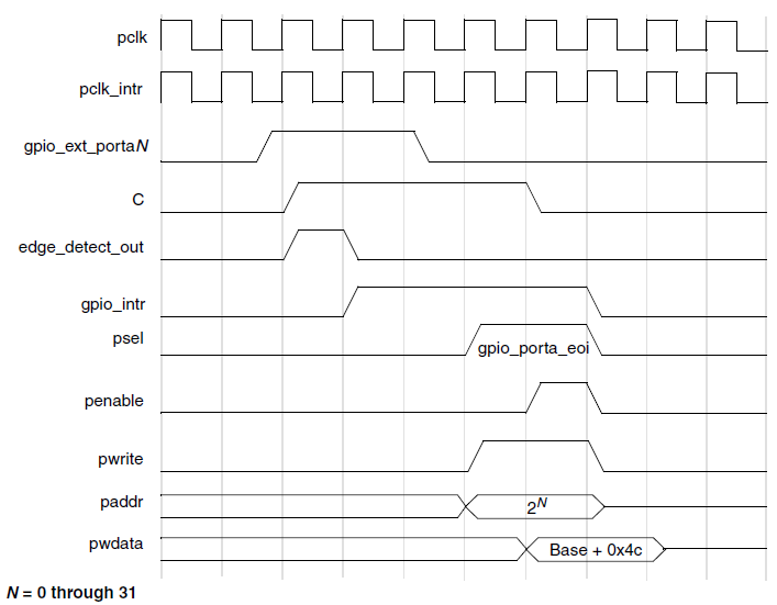
中断边沿检测与中断清除时序 (GPIO_SYNC_PA_INTERRUPTS = 0,移除亚稳态寄存器)
下图展示了消抖逻辑未被使用的场景。在该时序图中,meta_out 和 edge_detect_out 分别是第二个亚稳态寄存器和边沿检测逻辑的输出。第二次边沿检测发生在写入中断清除寄存器的同一周期。在此示例中,写入中断清除寄存器不会清除第二个中断,gpio_intr{_n} 信号不会被撤销。
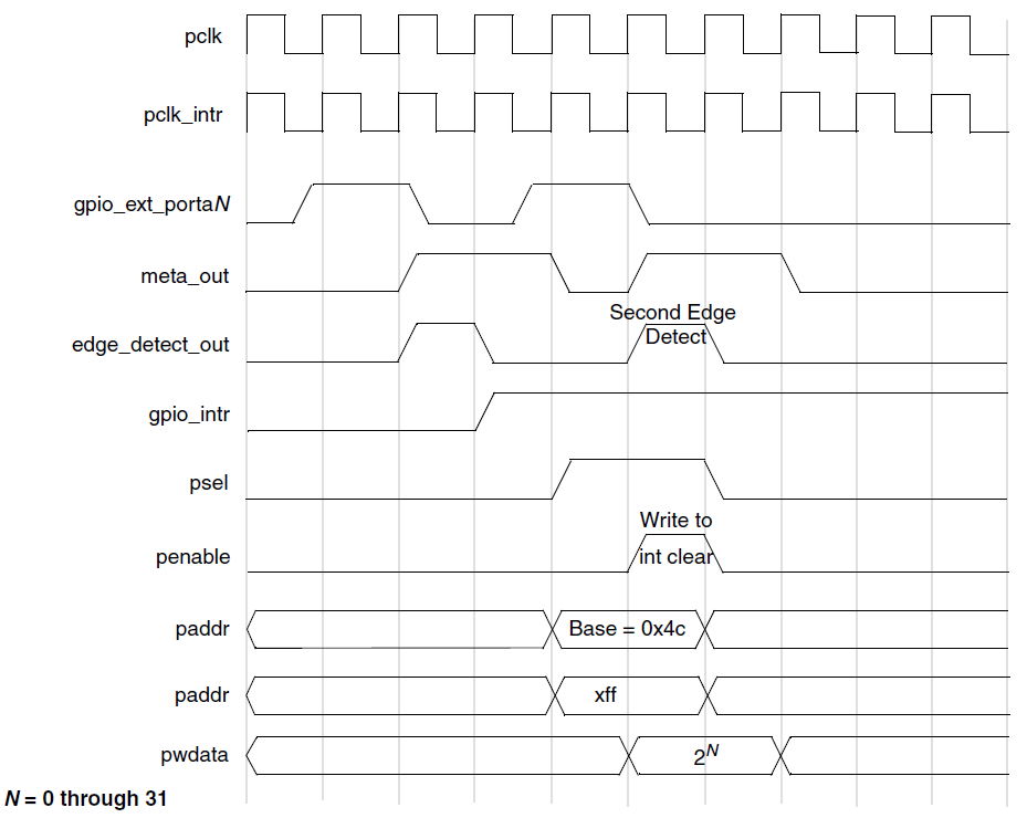
写入中断清除寄存器与新中断检测同时发生
双边沿检测
上升沿和下降沿的双边沿中断检测逻辑仅在 GPIO_INT_BOTHEDGE 寄存器被编程为 1 时才可用,此逻辑会同时检测上升沿和下降沿的中断。
下图展示了 gpio_ext_portaN 信号上中断源的同步和边沿检测中断生成。
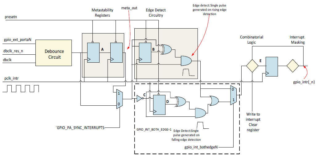
同步和边沿检测中断生成(GPIO_INT_BOTH_EDGE=1)
下图展示了一个时序图,其中在 Port A 输入的上升沿和下降沿均会产生中断,即 GPIO_INT_BOTH_EDGE = 1 且 GPIO_INT_BOTHEDGE 被编程为检测双边沿。
在此场景中,消抖(debounce)逻辑被禁用,并且包含亚稳态(metastability)寄存器。该图还展示了如何通过写中断清除寄存器来清除中断。
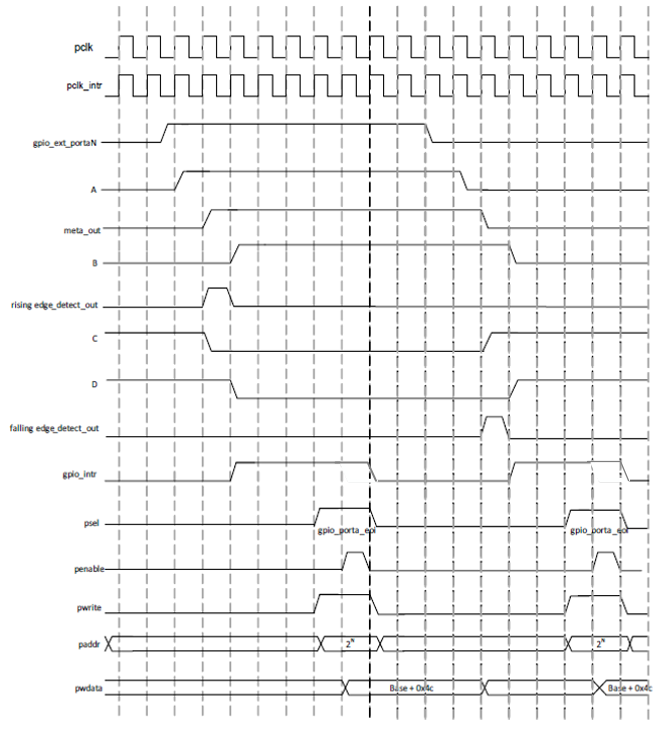
中断边沿检测和中断清除时序(GPIO_SYNC_PA_INTERRUPTS = 1 且 GPIO_INT_BOTH_EDGE =1,包含亚稳态寄存器)
下图展示了与图 interrupt_metastability_included 类似的时序图,不同之处在于此场景中移除了亚稳态寄存器。
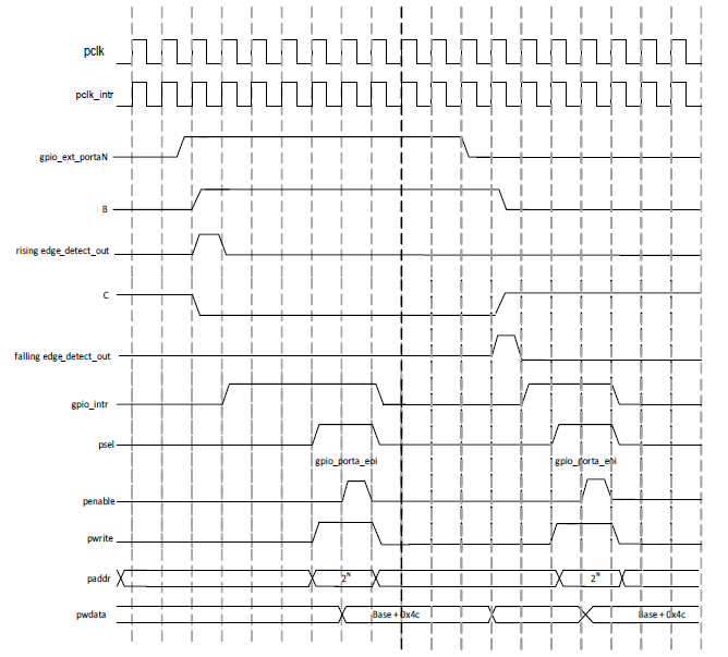
中断边沿检测和中断清除时序(GPIO_SYNC_PA_INTERRUPTS = 0 且 GPIO_INT_BOTH_EDGE =1,移除亚稳态寄存器)
电平触发中断
电平触发中断需要正确的中断服务程序 (ISR) 处理。ISR 可以轮询 GPIO_INT_STATUS_RAW 寄存器直到中断源被清除,或者在退出前通过 GPIO_INT_MASK 寄存器屏蔽中断。
如果 ISR 在退出前没有屏蔽中断,电平触发中断将会反复触发,直到中断源条件被消除。
下图展示了电平触发中断的生成过程。同时,下面的消抖电路是消抖或消除小于 2 个 dbclk 周期的虚假毛刺的示例。
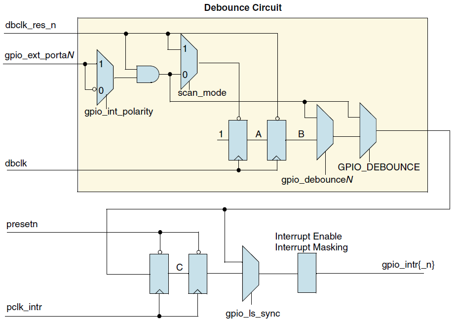
电平触发中断 RTL 原理图
对于电平触发中断,可以选择将其同步到中断时钟 pclk_intr,或者完全采用组合逻辑(消抖电路除外)。
该选择通过编程 GPIO_INT_LS_SYNC (GPIO 电平触发同步)寄存器来完成。
这是一个内存映射位,它会插入两个由 pclk_intr 驱动的亚稳态寄存器,以将电平触发中断同步到 pclk_intr。
当 GPIO_INT_LS_SYNC 未置位时,无法保证中断线与 pclk_intr 同步。可能需要设置处理器状态寄存器以指示异步中断。当 GPIO_INT_LS_SYNC 置位时,pclk_intr 时钟必须存在,才能将中断传递到中断控制器模块。
当选择将电平触发中断同步到 pclk_intr 时,gpio_intrclk_en 输出信号会被置位。gpio_intrclk_en 信号可用于时钟生成模块来开启 pclk_intr。
备注
在正常运行模式下,建议将 pclk_intr 同步到 pclk,以防止电路产生毛刺。
在睡眠模式下,如果需要更快的唤醒速度,可以禁用此同步。
下图展示了禁用消抖电路时低电平有效电平触发中断的生成过程。
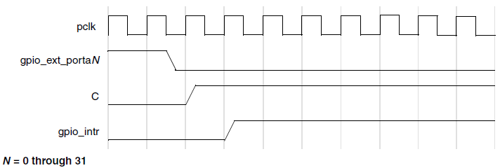
低电平有效电平触发中断生成时序图
消抖功能
如果用户配置了中断功能,可以通过 GPIO_DEBOUNCE 寄存器来配置 GPIO 是否包含消抖功能。外部信号可以进行消抖处理,以消除小于外部消抖时钟一个周期的任何毛刺。
下图展示了消抖电路的 RTL 示意图。时序图显示了 gpio_ext_portxN 上的高电平有效输入信号。输入信号检测的极性由存储器映射信号 gpio_int_polarity 控制。对于下降沿或低电平有效的输入,输入信号会被反相,然后使用与上升沿或高电平有效中断相同的消抖逻辑。
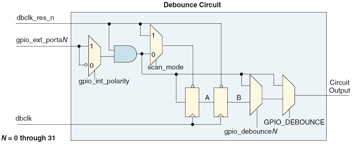
消抖 RTL 示意图
dbclk_res_n 信号相对于消抖时钟 dbclk 异步有效、同步释放。
presetn 为系统复位信号,相对于 pclk 异步有效、同步释放;同步必须在组件外部完成。
假设 pclk 和 dbclk 信号彼此异步。
当使用消抖时钟对输入中断信号进行消抖处理时,信号必须保持至少两个消抖时钟周期的有效状态,才能确保被正确锁存。任何小于消抖时钟周期的输入脉冲宽度都会被滤除。脉冲宽度在一到两个消抖时钟周期之间时,可能会也可能不会传播,具体取决于其与消抖时钟的相位关系。如果输入脉冲跨越消抖时钟的两个上升沿,则会被锁存;如果仅跨越一个上升沿,则不会被锁存。
下面的时序图展示了两种情况:输入信号被滤除,以及随后的输入信号被传播。如果 GPIO 支持消抖功能,则可以在软件控制下启用或禁用 Port A 上输入信号的消抖处理。
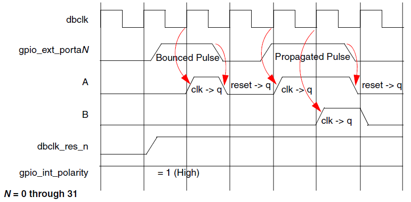
异步复位触发器消抖时序图
备注
使用消抖电路会使中断延迟增加两个消抖时钟周期。
消抖电路仅适用于异步复位触发器。
寄存器
Base Address: 0x41010000
Name |
Address offset |
Access |
Description |
|---|---|---|---|
000h |
R/W |
||
004h |
R/W |
||
008h |
R |
||
030h |
R/W |
||
038h |
R/W |
||
03Ch |
R/W |
||
040h |
R |
||
044h |
R |
||
048h |
R/W |
||
04Ch |
R/W |
||
050h |
R |
||
060h |
R/W |
||
064h |
R |
||
068h |
R/W |
||
06Ch |
R |
||
078h |
R |
REG_GPIO_DR
Name: PortA/B data register
Size: 32
Address offset: 000h
Read/write access: R/W
Bit |
Symbol |
Access |
INI |
Description |
|---|---|---|---|---|
31:0 |
PORT_DATA |
R/W |
0 |
Values written to this register are output on the I/O signals for Portx if the corresponding data direction bits for Portx are set to output mode and the corresponding control bit for Portx is set to software mode. The value read back equals to the last value written to this register. |
REG_GPIO_DDR
Name: PortA/B data direction register
Size: 32
Address offset: 004h
Read/write access: R/W
Bit |
Symbol |
Access |
INI |
Description |
|---|---|---|---|---|
31:0 |
PORT_DATA_DIRECTION |
R/W |
0 |
Values written to this register independently control the direction of the corresponding data bit in Portx. The default direction can be configured as input or output after system reset through the GPIO_DFLT_DIR_x parameter.
|
REG_GPIO_CTL
Name: PortA/B data source register
Size: 32
Address offset: 008h
Read/write access: R
Bit |
Symbol |
Access |
INI |
Description |
|---|---|---|---|---|
31:0 |
RSVD |
R |
- |
Reserved |
REG_GPIO_INT_EN
Name: PortA/B interrupt enable register
Size: 32
Address offset: 030h
Read/write access: R/W
Bit |
Symbol |
Access |
INI |
Description |
|---|---|---|---|---|
31:0 |
GPIO_INT_EN |
R/W |
0 |
Allows each bit of Portx to be configured for interrupts. By default, the generation of interrupts is disabled. Whenever a 1 is written to a bit of this register, it configures the corresponding bit on Portx to become an interrupt; otherwise, Portx operates as a normal GPIO signal. Interrupts are disabled on the corresponding bits of Portx if the corresponding data direction register is set to output or if Portx mode is set to hardware.
|
REG_GPIO_INT_TYPE
Name: PortA/B interrupt trigger type register
Size: 32
Address offset: 038h
Read/write access: R/W
Bit |
Symbol |
Access |
INI |
Description |
|---|---|---|---|---|
31:0 |
GPIO_INT_TYPE |
R/W |
0 |
Controls the type of interrupt that can occur on Portx. Whenever a 0 is written to a bit of this register, it configures the interrupt type to be level-sensitive; otherwise, it is edge-sensitive.
|
REG_GPIO_INT_POLARITY
Name: PortA/B interrupt polarity register
Size: 32
Address offset: 03Ch
Read/write access: R/W
Bit |
Symbol |
Access |
INI |
Description |
|---|---|---|---|---|
31:0 |
GPIO_INT_POLARITY |
R/W |
0 |
Controls the polarity of edge or level sensitivity that can occur on input of Portx. Whenever a 0 is written to a bit of this register, it configures the interrupt type to falling-edge or active-low sensitive; otherwise, it is rising-edge or active-high sensitive.
|
REG_GPIO_INT_STATUS
Name: PortA/B interrupt status register
Size: 32
Address offset: 040h
Read/write access: R
Bit |
Symbol |
Access |
INI |
Description |
|---|---|---|---|---|
31:0 |
GPIO_INT_STATUS |
R |
0 |
Interrupt status of Portx. |
REG_GPIO_INT_STATUS_RAW
Name: PortA/B raw interrupt status register
Size: 32
Address offset: 044h
Read/write access: R
Bit |
Symbol |
Access |
INI |
Description |
|---|---|---|---|---|
31:0 |
GPIO_RAW_INT_STATUS |
R |
0 |
Raw interrupt status of Portx (premasking bits). |
REG_GPIO_DEBOUNCE
Name: PortA/B interrupt debounce register
Size: 32
Address offset: 048h
Read/write access: R/W
Bit |
Symbol |
Access |
INI |
Description |
|---|---|---|---|---|
31:0 |
GPIO_DEBOUNCE_EN |
R/W |
0 |
Controls whether an external signal that is the source of an interrupt needs to be debounced to remove any spurious glitches. Writing a 1 to a bit in this register enables the debouncing circuitry. A signal must be valid for two periods of an external clock before it is internally processed.
This register is available only if Portx is configured to generate interrupts (GPIO_PORTA_INTR = Include(1)) and when the debounce logic is included (GPIO_DEBOUNCE = Include(1)). |
REG_GPIO_INT_EOI
Name: PortA/B edge type interrupt clear register
Size: 32
Address offset: 04Ch
Read/write access: R/W
Bit |
Symbol |
Access |
INI |
Description |
|---|---|---|---|---|
31:0 |
GPIO_INT_EOI |
R/W |
0 |
Controls the clearing of edge type interrupts from Portx. When a 1 is written into a corresponding bit of this register, the interrupt is cleared. All interrupts are cleared when Portx is not configured for interrupts.
|
REG_GPIO_EXT_PORT
Name: External PortA/B data register
Size: 32
Address offset: 050h
Read/write access: R
Bit |
Symbol |
Access |
INI |
Description |
|---|---|---|---|---|
31:0 |
GPIO_EXT_PORTA |
R |
0 |
When Portx is configured as Input, then reading this location reads the values on the signal. When the data direction of Portx is set as output, reading this location reads the data register for Portx. |
REG_GPIO_ITN_LS_SYNC
Name: PortA/B level interrupt synchronization
Size: 32
Address offset: 060h
Read/write access: R/W
Bit |
Symbol |
Access |
INI |
Description |
|---|---|---|---|---|
31:1 |
RSVD |
R |
- |
Reserved |
0 |
GPIO_LEVEL_SYNC |
R/W |
0 |
Writing a 1 to this register results in all level-sensitive interrupts being synchronized to pclk_intr.
|
REG_GPIO_ID_CODE
Name: PortA/B GPIO ID code register
Size: 32
Address offset: 064h
Read/write access: R
Bit |
Symbol |
Access |
INI |
Description |
|---|---|---|---|---|
31:0 |
GPIO_ID_CODE |
R |
32'h1 |
This register is available only if Portx is configured to generate interrupts (GPIO_PORTx_INTR = Include(1)) and interrupt detection is configured to generate on both rising and falling edges of external input signal (GPIO_INT_BOTH_EDGE=Include(1)). |
REG_GPIO_INT_BOTHEDGE
Name: PortA/B both edge interrupt register
Size: 32
Address offset: 068h
Read/write access: R/W
Bit |
Symbol |
Access |
INI |
Description |
|---|---|---|---|---|
31:0 |
GPIO_INT_BOTHEDGE |
R/W |
0 |
Controls the edge types of interrupt that can occur on Portx. Whenever a particular bit is programmed to 1, it enables the generation of interrupt on both the rising edge and falling edge of an external input signal corresponding to that bit on Portx. The values programmed in the registers gpio_intype_level and gpio_int_polarity for this particular bit are not considered when the corresponding bit of this register is set to 1. Whenever a particular bit is programmed to 0, the interrupt type depends on the value of the corresponding bits in the gpio_inttype_level and gpio_int_polarity registers.
|
REG_GPIO_VER_ID_CODE
Name: PortA/B GPIO component version register
Size: 32
Address offset: 06Ch
Read/write access: R
Bit |
Symbol |
Access |
INI |
Description |
|---|---|---|---|---|
31:0 |
GPIO_VER_ID_CODE |
R |
32'h3231302A |
ASCII value for each number in the version, followed by *. For example, 32_30_31_2A represents the version 2.01*. |
REG_GPIO_DB_DIV_CONFIG
Size: 32
Address offset: 078h
Read/write access: R
Bit |
Symbol |
Access |
INI |
Description |
|---|---|---|---|---|
31:0 |
RSVD |
R |
- |
Reserved |
Base Address: 0x4101A000
Name |
Address offset |
Access |
Description |
|---|---|---|---|
000h |
R/W |
||
004h |
R/W |
||
008h |
R |
||
030h |
R/W |
||
034h |
R/W |
||
038h |
R/W |
||
03Ch |
R/W |
||
040h |
R |
||
044h |
R |
||
048h |
R/W |
||
04Ch |
R/W |
||
050h |
R |
||
060h |
R/W |
||
064h |
R |
||
068h |
R/W |
||
06Ch |
R |
REG_GPIO_DR
Name: PortA/B data register
Size: 32
Address offset: 000h
Read/write access: R/W
Bit |
Symbol |
Access |
INI |
Description |
|---|---|---|---|---|
31:0 |
PORT_DATA |
R/W |
0 |
Values written to this register are output on the I/O signals for Portx if the corresponding data direction bits for Portx are set to Output mode and the corresponding control bit for Portx is set to software mode. The value read back is equal to the last value written to this register. Valid bits is: PortA[31:0] and PortB[19:0]. |
REG_GPIO_DDR
Name: PortA/B data direction register
Size: 32
Address offset: 004h
Read/write access: R/W
Bit |
Symbol |
Access |
INI |
Description |
|---|---|---|---|---|
31:0 |
PORT_DATA_DIRECTION |
R/W |
0 |
Values written to this register independently control the direction of the corresponding data bit in Portx. The default direction can be configured as input or output after system reset through the GPIO_DFLT_DIR_x parameter.
Valid bits is: PortA[31:0] and PortB[19:0]. |
REG_GPIO_CTL
Name: PortA/B data source register
Size: 32
Address offset: 008h
Read/write access: R
Bit |
Symbol |
Access |
INI |
Description |
|---|---|---|---|---|
31:0 |
RSVD |
R |
- |
Reserved |
REG_GPIO_INT_EN
Name: PortA/B interrupt enable register
Size: 32
Address offset: 030h
Read/write access: R/W
Bit |
Symbol |
Access |
INI |
Description |
|---|---|---|---|---|
31:0 |
GPIO_INT_EN |
R/W |
0 |
Allows each bit of Portx to be configured for interrupts. By default, the generation of interrupts is disabled. Whenever a 1 is written to a bit of this register, it configures the corresponding bit on Portx to become an interrupt; otherwise, Portx operates as a normal GPIO signal. Interrupts are disabled on the corresponding bits of Portx if the corresponding data direction register is set to Output or if Portx mode is set to Hardware.
|
REG_GPIO_INT_MASK
Name: PortA/B interrupt mask register
Size: 32
Address offset: 034h
Read/write access: R/W
Bit |
Symbol |
Access |
INI |
Description |
|---|---|---|---|---|
31:0 |
GPIO_INT_MASK |
R/W |
0 |
Controls whether an interrupt on Portx can create an interrupt for the interrupt controller by not masking it. By default, all interrupts bits are unmasked. Whenever a 1 is written to a bit in this register, it masks the interrupt generation capability for this signal; otherwise interrupts are allowed through. The unmasked status can be read as well as the resultant status after masking.
|
REG_GPIO_INT_TYPE
Name: PortA interrupt trigger type register
Size: 32
Address offset: 038h
Read/write access: R/W
Bit |
Symbol |
Access |
INI |
Description |
|---|---|---|---|---|
31:0 |
GPIO_INT_TYPE |
R/W |
0 |
Controls the type of interrupt that can occur on Portx. Whenever a 0 is written to a bit of this register, it configures the interrupt type to be level-sensitive; otherwise, it is edge-sensitive.
|
REG_GPIO_INT_POLARITY
Name: PortA interrupt polarity register
Size: 32
Address offset: 03Ch
Read/write access: R/W
Bit |
Symbol |
Access |
INI |
Description |
|---|---|---|---|---|
31:0 |
GPIO_INT_POLARITY |
R/W |
0 |
Controls the polarity of edge or level sensitivity that can occur on input of Portx. Whenever a 0 is written to a bit of this register, it configures the interrupt type to falling-edge or active-low sensitive; otherwise, it is rising-edge or active-high sensitive.
|
REG_GPIO_INT_STATUS
Name: PortA/B interrupt status register
Size: 32
Address offset: 040h
Read/write access: R
Bit |
Symbol |
Access |
INI |
Description |
|---|---|---|---|---|
31:0 |
GPIO_INT_STATUS |
R |
0 |
Interrupt status of Portx. |
REG_GPIO_INT_STATUS_RAW
Name: PortA/B raw interrupt status register
Size: 32
Address offset: 044h
Read/write access: R
Bit |
Symbol |
Access |
INI |
Description |
|---|---|---|---|---|
31:0 |
GPIO_RAW_INT_STATUS |
R |
0 |
Raw interrupt status of Portx (premasking bits). |
REG_GPIO_DEBOUNCE
Name: PortA/B interrupt debounce register
Size: 32
Address offset: 048h
Read/write access: R/W
Bit |
Symbol |
Access |
INI |
Description |
|---|---|---|---|---|
31:0 |
GPIO_DEBOUNCE_EN |
R/W |
0 |
Controls whether an external signal that is the source of an interrupt needs to be debounced to remove any spurious glitches. Writing a 1 to a bit in this register enables the debouncing circuitry. A signal must be valid for two periods of an external clock before it is internally Processed.
This register is available only if Portx is configured to generate interrupts (GPIO_PORTA_INTR = Include (1)) and when the debounce logic is included (GPIO_DEBOUNCE = Include (1)). |
REG_GPIO_INT_EOI
Name: PortA/B edge type interrupt clear register
Size: 32
Address offset: 04Ch
Read/write access: R/W
Bit |
Symbol |
Access |
INI |
Description |
|---|---|---|---|---|
31:0 |
GPIO_INT_EOI |
R/W |
0 |
Controls the clearing of edge type interrupts from Portx. When a 1 is written into a corresponding bit of this register, the interrupt is cleared. All interrupts are cleared when Portx is not configured for interrupts.
|
REG_GPIO_EXT_PORT
Name: External PortA/B data register
Size: 32
Address offset: 050h
Read/write access: R
Bit |
Symbol |
Access |
INI |
Description |
|---|---|---|---|---|
31:0 |
GPIO_EXT_PORTA |
R |
0 |
When Portx is configured as Input, then reading this location reads the values on the signal. When the data direction of Portx is set as Output, reading this location reads the data register for Portx. |
REG_GPIO_ITN_LS_SYNC
Name: PortA/B level interrupt synchronization
Size: 32
Address offset: 060h
Read/write access: R/W
Bit |
Symbol |
Access |
INI |
Description |
|---|---|---|---|---|
31:1 |
RSVD |
R |
- |
Reserved |
0 |
GPIO_LEVEL_SYNC |
R/W |
0 |
Writing a 1 to this register results in all level-sensitive interrupts being synchronized to pclk_intr.
|
REG_GPIO_ID_CODE
Name: PortA/B GPIO ID code register
Size: 32
Address offset: 064h
Read/write access: R
Bit |
Symbol |
Access |
INI |
Description |
|---|---|---|---|---|
31:0 |
GPIO_ID_CODE |
R |
32'h1 |
This register is available only if PortxA/B is configured to generate interrupts (GPIO_PORTx_INTR = Include (1)) and interrupt detection is configured to generate on both rising and falling edges of external input signal (GPIO_INT_BOTH_EDGE=Include (1)). |
REG_GPIO_INT_BOTHEDGE
Name: PortA/B both edge interrupt register
Size: 32
Address offset: 068h
Read/write access: R/W
Bit |
Symbol |
Access |
INI |
Description |
|---|---|---|---|---|
31:0 |
GPIO_INT_BOTHEDGE |
R/W |
0 |
Controls the edge types of interrupt that can occur on Portx. Whenever a particular bit is programmed to 1, it enables the generation of interrupt on both the rising edge and falling edge of an external input signal corresponding to that bit on PortA. The values programmed in the registers gpio_intype_level and gpio_int_polarity for this particular bit are not considered when the corresponding bit of this register is set to 1. Whenever a particular bit is programmed to 0, the interrupt type depends on the value of the corresponding bits in the gpio_inttype_level and gpio_int_polarity registers.
|
REG_GPIO_VER_ID_CODE
Name: PortA/B GPIO component version register
Size: 32
Address offset: 06Ch
Read/write access: R
Bit |
Symbol |
Access |
INI |
Description |
|---|---|---|---|---|
31:0 |
GPIO_VER_ID_CODE |
R |
32'h3231302A |
ASCII value for each number in the version, followed by *. For example 32_30_31_2A represents the version 2.01*. Reset Value: See the releases table in the Release Notes. |
REGISTER_CONTENTS=RTL8720E
REGISTER_CONTENTS=RTL8720E
REGISTER_CONTENTS=RTL8720E
Base Address: 0x4200D000
Name |
Address offset |
Access |
Description |
|---|---|---|---|
000h |
R/W |
||
004h |
R/W |
||
008h |
R |
||
030h |
R/W |
||
034h |
R/W |
||
038h |
R/W |
||
03Ch |
R/W |
||
040h |
R |
||
044h |
R |
||
048h |
R/W |
||
04Ch |
R/W |
||
050h |
R |
||
060h |
R/W |
||
064h |
R |
||
068h |
R/W |
||
06Ch |
R |
||
078h |
R/W |
REG_GPIO_DR
Name: PortA data register
Size: 32
Address offset: 000h
Read/write access: R/W
Bit |
Symbol |
Access |
INI |
Description |
|---|---|---|---|---|
31:0 |
PORTA_DATA |
R/W |
0 |
Values written to this register are output on the I/O signals for Portx if the corresponding data direction bits for Portx are set to Output mode and the corresponding control bit for Portx is set to software mode. The value read back is equal to the last value written to this register. |
REG_GPIO_DDR
Name: PortA data direction register
Size: 32
Address offset: 004h
Read/write access: R/W
Bit |
Symbol |
Access |
INI |
Description |
|---|---|---|---|---|
31:0 |
PORTA_DATA_DIRECTION |
R/W |
0 |
Values written to this register independently control the direction of the corresponding data bit in Portx. The default direction can be configured as input or output after system reset through the GPIO_DFLT_DIR_x parameter.
|
REG_GPIO_CTL
Name: PortA data source register
Size: 32
Address offset: 008h
Read/write access: R
Bit |
Symbol |
Access |
INI |
Description |
|---|---|---|---|---|
31:0 |
RSVD |
R |
- |
Reserved |
REG_GPIO_INT_EN
Name: PortA/B/C interrupt enable register
Size: 32
Address offset: 030h
Read/write access: R/W
Bit |
Symbol |
Access |
INI |
Description |
|---|---|---|---|---|
31:0 |
GPIO_INT_EN |
R/W |
0 |
Allows each bit of Portx to be configured for interrupts. By default, the generation of interrupts is disabled. Whenever a 1 is written to a bit of this register, it configures the corresponding bit on Portx to become an interrupt; otherwise, Portx operates as a normal GPIO signal. Interrupts are disabled on the corresponding bits of Portx if the corresponding data direction register is set to Output or if Portx mode is set to Hardware.
|
REG_GPIO_INT_MASK
Name: PortA/B/C interrupt mask register
Size: 32
Address offset: 034h
Read/write access: R/W
Bit |
Symbol |
Access |
INI |
Description |
|---|---|---|---|---|
31:0 |
GPIO_INT_MASK |
R/W |
0 |
Controls whether an interrupt on Portx can create an interrupt for the interrupt controller by not masking it. By default, all interrupts bits are unmasked. Whenever a 1 is written to a bit in this register, it masks the interrupt generation capability for this signal; otherwise interrupts are allowed through. The unmasked status can be read as well as the resultant status after masking.
|
REG_GPIO_INT_TYPE
Name: PortA interrupt trigger type register
Size: 32
Address offset: 038h
Read/write access: R/W
Bit |
Symbol |
Access |
INI |
Description |
|---|---|---|---|---|
31:0 |
GPIO_INT_TYPE |
R/W |
0 |
Controls the type of interrupt that can occur on Portx. Whenever a 0 is written to a bit of this register, it configures the Interrupt type to be level-sensitive; otherwise, it is edge-sensitive.
|
REG_GPIO_INT_POLARITY
Name: PortA interrupt polarity register
Size: 32
Address offset: 03Ch
Read/write access: R/W
Bit |
Symbol |
Access |
INI |
Description |
|---|---|---|---|---|
31:0 |
GPIO_INT_POLARITY |
R/W |
0 |
Controls the polarity of edge or level sensitivity that can occur on input of Portx. Whenever a 0 is written to a bit of this register, it configures the interrupt type to falling-edge or active-low sensitive; otherwise, it is rising-edge or active-high sensitive.
|
REG_GPIO_INT_STATUS
Name: PortA/B/C interrupt status register
Size: 32
Address offset: 040h
Read/write access: R
Bit |
Symbol |
Access |
INI |
Description |
|---|---|---|---|---|
31:0 |
GPIO_INT_STATUS |
R |
0 |
Interrupt status of Portx. |
REG_GPIO_INT_STATUS_RAW
Name: PortA/B/C raw interrupt status register
Size: 32
Address offset: 044h
Read/write access: R
Bit |
Symbol |
Access |
INI |
Description |
|---|---|---|---|---|
31:0 |
GPIO_RAW_INT_STATUS |
R |
0 |
Raw interrupt status of Portx (premasking bits). |
REG_GPIO_DEBOUNCE
Name: PortA/B/C interrupt debounce register
Size: 32
Address offset: 048h
Read/write access: R/W
Bit |
Symbol |
Access |
INI |
Description |
|---|---|---|---|---|
31:0 |
GPIO_DEBOUNCE_EN |
R/W |
0 |
Controls whether an external signal that is the source of an interrupt needs to be debounced to remove any spurious glitches. Writing a 1 to a bit in this register enables the debouncing circuitry. A signal must be valid for two periods of an external clock before it is internally Processed.
This register is available only if Portx is configured to generate interrupts (GPIO_PORTA_INTR = Include (1)) and when the debounce logic is included (GPIO_DEBOUNCE = Include (1)). |
REG_GPIO_INT_EOI
Name: PortA/B/C edge type interrupt clear register
Size: 32
Address offset: 04Ch
Read/write access: R/W
Bit |
Symbol |
Access |
INI |
Description |
|---|---|---|---|---|
31:0 |
GPIO_INT_EOI |
R/W |
0 |
Controls the clearing of edge type interrupts from Portx. When a 1 is written into a corresponding bit of this register, the interrupt is cleared. All interrupts are cleared when Portx is not configured for interrupts.
|
REG_GPIO_EXT_PORT
Name: External PortA/B/C data register
Size: 32
Address offset: 050h
Read/write access: R
Bit |
Symbol |
Access |
INI |
Description |
|---|---|---|---|---|
31:0 |
GPIO_EXT_PORTA |
R |
0 |
When Portx is configured as Input, then reading this location reads the values on the signal. When the data direction of Portx is set as Output, reading this location reads the data register for Portx. |
REG_GPIO_ITN_LS_SYNC
Name: PortA/B/C level interrupt synchronization
Size: 32
Address offset: 060h
Read/write access: R/W
Bit |
Symbol |
Access |
INI |
Description |
|---|---|---|---|---|
31:1 |
RSVD |
R |
- |
Reserved |
0 |
GPIO_LEVEL_SYNC |
R/W |
0 |
Writing a 1 to this register results in all level-sensitive interrupts being synchronized to pclk_intr.
|
REG_GPIO_ID_CODE
Name: PortA/B/C GPIO ID code register
Size: 32
Address offset: 064h
Read/write access: R
Bit |
Symbol |
Access |
INI |
Description |
|---|---|---|---|---|
31:0 |
GPIO_ID_CODE |
R |
32'h1 |
This register is available only if Portx/B/C is configured to generate interrupts (GPIO_PORTx_INTR = Include (1)) and interrupt detection is configured to generate on both rising and falling edges of external input signal (GPIO_INT_BOTH_EDGE=Include (1)). |
REG_GPIO_INT_BOTHEDGE
Name: PortA/B/C both edge interrupt register
Size: 32
Address offset: 068h
Read/write access: R/W
Bit |
Symbol |
Access |
INI |
Description |
|---|---|---|---|---|
31:0 |
GPIO_INT_BOTHEDGE |
R/W |
0 |
Controls the edge types of interrupt that can occur on Portx. Whenever a particular bit is programmed to 1, it enables the generation of interrupt on both the rising edge and falling edge of an external input signal corresponding to that bit on PortA. The values programmed in the registers gpio_intype_level and gpio_int_polarity for this particular bit are not considered when the corresponding bit of this register is set to 1. Whenever a particular bit is programmed to 0, the interrupt type depends on the value of the corresponding bits in the gpio_inttype_level and gpio_int_polarity registers.
|
REG_GPIO_VER_ID_CODE
Name: PortA/B/C GPIO component version register
Size: 32
Address offset: 06Ch
Read/write access: R
Bit |
Symbol |
Access |
INI |
Description |
|---|---|---|---|---|
31:0 |
GPIO_VER_ID_CODE |
R |
32'h3231302A |
ASCII value for each number in the version, followed by *. For example 32_30_31_2A represents the version 2.01*. Reset Value: See the releases table in the Release Notes. |
REG_GPIO_DB_DIV_CONFIG
Size: 32
Address offset: 078h
Read/write access: R/W
Bit |
Symbol |
Access |
INI |
Description |
|---|---|---|---|---|
31:7 |
RSVD |
R |
- |
Reserved |
6:0 |
EXT_DB_DIV_CNT |
R/W |
0 |
Debounce interrupt prescaler of 32.768KHz. De-bounce time = (EXT_DB_DIV_CNT +1) * 2*32μs. |
Base Address: 0x40811000
Name |
Address offset |
Access |
Description |
|---|---|---|---|
000h |
R/W |
||
004h |
R/W |
||
008h |
R |
||
030h |
R/W |
||
034h |
R/W |
||
038h |
R/W |
||
03Ch |
R/W |
||
040h |
R |
||
044h |
R |
||
048h |
R/W |
||
04Ch |
R/W |
||
050h |
R |
||
060h |
R/W |
||
064h |
R |
||
068h |
R/W |
||
06Ch |
R |
||
078h |
R |
||
0FCh |
R |
REG_GPIO_DR
Name: Port data register
Size: 32
Address offset: 000h
Read/write access: R/W
Bit |
Symbol |
Access |
INI |
Description |
|---|---|---|---|---|
31:0 |
PORT_DATA |
R/W |
0 |
Values written to this register are output on the I/O signals for Portx if the corresponding data direction bits for Portx are set to Output mode and the corresponding control bit for Portx is set to software mode. The value read back is equal to the last value written to this register. |
REG_GPIO_DDR
Name: Port data direction register
Size: 32
Address offset: 004h
Read/write access: R/W
Bit |
Symbol |
Access |
INI |
Description |
|---|---|---|---|---|
31:0 |
PORT_DATA_DIRECTION |
R/W |
0 |
Values written to this register independently control the direction of the corresponding data bit in Portx. The default direction can be configured as input or output after system reset through the GPIO_DFLT_DIR_x parameter.
|
REG_GPIO_CTL
Name: Port data source register
Size: 32
Address offset: 008h
Read/write access: R
Bit |
Symbol |
Access |
INI |
Description |
|---|---|---|---|---|
31:0 |
RSVD |
R |
- |
Reserved |
REG_GPIO_INT_EN
Name: Port interrupt enable register
Size: 32
Address offset: 030h
Read/write access: R/W
Bit |
Symbol |
Access |
INI |
Description |
|---|---|---|---|---|
31:0 |
GPIO_INT_EN |
R/W |
0 |
Allows each bit of Portx to be configured for interrupts. By default, the generation of interrupts is disabled. Whenever a 1 is written to a bit of this register, it configures the corresponding bit on Portx to become an interrupt; otherwise, Portx operates as a normal GPIO signal. Interrupts are disabled on the corresponding bits of Portx if the corresponding data direction register is set to Output or if Portx mode is set to Hardware.
|
REG_GPIO_INT_MASK
Name: Port interrupt mask register
Size: 32
Address offset: 034h
Read/write access: R/W
Bit |
Symbol |
Access |
INI |
Description |
|---|---|---|---|---|
31:0 |
GPIO_INT_MASK |
R/W |
0 |
Controls whether an interrupt on Portx can create an interrupt for the interrupt controller by not masking it. By default, all interrupts bits are unmasked. Whenever a 1 is written to a bit in this register, it masks the interrupt generation capability for this signal; otherwise interrupts are allowed through. The unmasked status can be read as well as the resultant status after masking.
|
REG_GPIO_INT_TYPE
Name: Port interrupt trigger type register
Size: 32
Address offset: 038h
Read/write access: R/W
Bit |
Symbol |
Access |
INI |
Description |
|---|---|---|---|---|
31:0 |
GPIO_INT_TYPE |
R/W |
0 |
Controls the type of interrupt that can occur on Portx. Whenever a 0 is written to a bit of this register, it configures the Interrupt type to be level-sensitive; otherwise, it is edge-sensitive.
|
REG_GPIO_INT_POLARITY
Name: Port interrupt polarity register
Size: 32
Address offset: 03Ch
Read/write access: R/W
Bit |
Symbol |
Access |
INI |
Description |
|---|---|---|---|---|
31:0 |
GPIO_INT_POLARITY |
R/W |
0 |
Controls the polarity of edge or level sensitivity that can occur on input of Portx. Whenever a 0 is written to a bit of this register, it configures the interrupt type to falling-edge or active-low sensitive; otherwise, it is rising-edge or active-high sensitive.
|
REG_GPIO_INT_STATUS
Name: Port interrupt status register
Size: 32
Address offset: 040h
Read/write access: R
Bit |
Symbol |
Access |
INI |
Description |
|---|---|---|---|---|
31:0 |
GPIO_INT_STATUS |
R |
0 |
Interrupt status of Portx. |
REG_GPIO_INT_STATUS_RAW
Name: Port raw interrupt status register
Size: 32
Address offset: 044h
Read/write access: R
Bit |
Symbol |
Access |
INI |
Description |
|---|---|---|---|---|
31:0 |
GPIO_RAW_INT_STATUS |
R |
0 |
Raw interrupt status of Portx (premasking bits). |
REG_GPIO_DEBOUNCE
Name: Port interrupt debounce register
Size: 32
Address offset: 048h
Read/write access: R/W
Bit |
Symbol |
Access |
INI |
Description |
|---|---|---|---|---|
31:0 |
GPIO_DEBOUNCE_EN |
R/W |
0 |
Controls whether an external signal that is the source of an interrupt needs to be debounced to remove any spurious glitches. Writing a 1 to a bit in this register enables the debouncing circuitry. A signal must be valid for two periods of an external clock before it is internally Processed.
This register is available only if Portx is configured to generate interrupts (GPIO_PORTA_INTR = Include (1)) and when the debounce logic is included (GPIO_DEBOUNCE = Include (1)). |
REG_GPIO_INT_EOI
Name: Port edge type interrupt clear register
Size: 32
Address offset: 04Ch
Read/write access: R/W
Bit |
Symbol |
Access |
INI |
Description |
|---|---|---|---|---|
31:0 |
GPIO_INT_EOI |
R/W |
0 |
Controls the clearing of edge type interrupts from Portx. When a 1 is written into a corresponding bit of this register, the interrupt is cleared. All interrupts are cleared when Portx is not configured for interrupts.
|
REG_GPIO_EXT_PORT
Name: External Port data register
Size: 32
Address offset: 050h
Read/write access: R
Bit |
Symbol |
Access |
INI |
Description |
|---|---|---|---|---|
31:0 |
GPIO_EXT_PORTA |
R |
0 |
When Portx is configured as Input, then reading this location reads the values on the signal. When the data direction of Portx is set as Output, reading this location reads the data register for Portx. |
REG_GPIO_ITN_LS_SYNC
Name: Port level interrupt synchronization
Size: 32
Address offset: 060h
Read/write access: R/W
Bit |
Symbol |
Access |
INI |
Description |
|---|---|---|---|---|
31:1 |
RSVD |
R |
- |
Reserved |
0 |
GPIO_LEVEL_SYNC |
R/W |
0 |
Writing a 1 to this register results in all level-sensitive interrupts being synchronized to pclk_intr.
|
REG_GPIO_ID_CODE
Name: Port GPIO ID code register
Size: 32
Address offset: 064h
Read/write access: R
Bit |
Symbol |
Access |
INI |
Description |
|---|---|---|---|---|
31:0 |
GPIO_ID_CODE |
R |
32'h1 |
This register is available only if Portx is configured to generate interrupts (GPIO_PORTx_INTR = Include (1)) and interrupt detection is configured to generate on both rising and falling edges of external input signal (GPIO_INT_BOTH_EDGE=Include (1)). |
REG_GPIO_INT_BOTHEDGE
Name: Port both edge interrupt register
Size: 32
Address offset: 068h
Read/write access: R/W
Bit |
Symbol |
Access |
INI |
Description |
|---|---|---|---|---|
31:0 |
GPIO_INT_BOTHEDGE |
R/W |
0 |
Controls the edge types of interrupt that can occur on Portx. Whenever a particular bit is programmed to 1, it enables the generation of interrupt on both the rising edge and falling edge of an external input signal corresponding to that bit on Port. The values programmed in the registers gpio_intype_level and gpio_int_polarity for this particular bit are not considered when the corresponding bit of this register is set to 1. Whenever a particular bit is programmed to 0, the interrupt type depends on the value of the corresponding bits in the gpio_inttype_level and gpio_int_polarity registers.
|
REG_GPIO_VER_ID_CODE
Name: Port GPIO component version register
Size: 32
Address offset: 06Ch
Read/write access: R
Bit |
Symbol |
Access |
INI |
Description |
|---|---|---|---|---|
31:0 |
GPIO_VER_ID_CODE |
R |
32'h3231302A |
ASCII value for each number in the version, followed by *. For example 32_30_31_2A represents the version 2.01*. Reset Value: See the releases table in the Release Notes. |
REG_GPIO_DB_DIV_CONFIG
Size: 32
Address offset: 078h
Read/write access: R
Bit |
Symbol |
Access |
INI |
Description |
|---|---|---|---|---|
31:0 |
RSVD |
R |
- |
Reserved |
REG_GPIO_DUMMY
Size: 32
Address offset: 0FCh
Read/write access: R
Bit |
Symbol |
Access |
INI |
Description |
|---|---|---|---|---|
31:16 |
RSVD |
R |
- |
Reserved |
15:0 |
DUMMY |
R |
0 |
No real reg, only for run_espec.py |
Base Address: 0x40802000
Name |
Address offset |
Access |
Description |
|---|---|---|---|
000h |
R/W |
||
004h |
R/W |
||
008h |
R |
||
030h |
R/W |
||
034h |
R/W |
||
038h |
R/W |
||
03Ch |
R/W |
||
040h |
R |
||
044h |
R |
||
048h |
R/W |
||
04Ch |
R/W |
||
050h |
R |
||
060h |
R/W |
||
064h |
R |
||
068h |
R/W |
||
06Ch |
R |
||
078h |
R |
||
0FCh |
R |
REG_GPIO_DR
Name: Port data register
Size: 32
Address offset: 000h
Read/write access: R/W
Bit |
Symbol |
Access |
INI |
Description |
|---|---|---|---|---|
31:0 |
PORT_DATA |
R/W |
0 |
Values written to this register are output on the I/O signals for Portx if the corresponding data direction bits for Portx are set to Output mode and the corresponding control bit for Portx is set to software mode. The value read back is equal to the last value written to this register. |
REG_GPIO_DDR
Name: Port data direction register
Size: 32
Address offset: 004h
Read/write access: R/W
Bit |
Symbol |
Access |
INI |
Description |
|---|---|---|---|---|
31:0 |
PORT_DATA_DIRECTION |
R/W |
0 |
Values written to this register independently control the direction of the corresponding data bit in Portx. The default direction can be configured as input or output after system reset through the GPIO_DFLT_DIR_x parameter.
|
REG_GPIO_CTL
Name: Port data source register
Size: 32
Address offset: 008h
Read/write access: R
Bit |
Symbol |
Access |
INI |
Description |
|---|---|---|---|---|
31:0 |
RSVD |
R |
- |
Reserved |
REG_GPIO_INT_EN
Name: Port interrupt enable register
Size: 32
Address offset: 030h
Read/write access: R/W
Bit |
Symbol |
Access |
INI |
Description |
|---|---|---|---|---|
31:0 |
GPIO_INT_EN |
R/W |
0 |
Allows each bit of Portx to be configured for interrupts. By default, the generation of interrupts is disabled. Whenever a 1 is written to a bit of this register, it configures the corresponding bit on Portx to become an interrupt; otherwise, Portx operates as a normal GPIO signal. Interrupts are disabled on the corresponding bits of Portx if the corresponding data direction register is set to Output or if Portx mode is set to Hardware.
|
REG_GPIO_INT_MASK
Name: Port interrupt mask register
Size: 32
Address offset: 034h
Read/write access: R/W
Bit |
Symbol |
Access |
INI |
Description |
|---|---|---|---|---|
31:0 |
GPIO_INT_MASK |
R/W |
0 |
Controls whether an interrupt on Portx can create an interrupt for the interrupt controller by not masking it. By default, all interrupts bits are unmasked. Whenever a 1 is written to a bit in this register, it masks the interrupt generation capability for this signal; otherwise interrupts are allowed through. The unmasked status can be read as well as the resultant status after masking.
|
REG_GPIO_INT_TYPE
Name: Port interrupt trigger type register
Size: 32
Address offset: 038h
Read/write access: R/W
Bit |
Symbol |
Access |
INI |
Description |
|---|---|---|---|---|
31:0 |
GPIO_INT_TYPE |
R/W |
0 |
Controls the type of interrupt that can occur on Portx. Whenever a 0 is written to a bit of this register, it configures the Interrupt type to be level-sensitive; otherwise, it is edge-sensitive.
|
REG_GPIO_INT_POLARITY
Name: Port interrupt polarity register
Size: 32
Address offset: 03Ch
Read/write access: R/W
Bit |
Symbol |
Access |
INI |
Description |
|---|---|---|---|---|
31:0 |
GPIO_INT_POLARITY |
R/W |
0 |
Controls the polarity of edge or level sensitivity that can occur on input of Portx. Whenever a 0 is written to a bit of this register, it configures the interrupt type to falling-edge or active-low sensitive; otherwise, it is rising-edge or active-high sensitive.
|
REG_GPIO_INT_STATUS
Name: Port interrupt status register
Size: 32
Address offset: 040h
Read/write access: R
Bit |
Symbol |
Access |
INI |
Description |
|---|---|---|---|---|
31:0 |
GPIO_INT_STATUS |
R |
0 |
Interrupt status of Portx. |
REG_GPIO_INT_STATUS_RAW
Name: Port raw interrupt status register
Size: 32
Address offset: 044h
Read/write access: R
Bit |
Symbol |
Access |
INI |
Description |
|---|---|---|---|---|
31:0 |
GPIO_RAW_INT_STATUS |
R |
0 |
Raw interrupt status of Portx (premasking bits). |
REG_GPIO_DEBOUNCE
Name: Port interrupt debounce register
Size: 32
Address offset: 048h
Read/write access: R/W
Bit |
Symbol |
Access |
INI |
Description |
|---|---|---|---|---|
31:0 |
GPIO_DEBOUNCE_EN |
R/W |
0 |
Controls whether an external signal that is the source of an interrupt needs to be debounced to remove any spurious glitches. Writing a 1 to a bit in this register enables the debouncing circuitry. A signal must be valid for two periods of an external clock before it is internally Processed.
This register is available only if Portx is configured to generate interrupts (GPIO_PORTA_INTR = Include (1)) and when the debounce logic is included (GPIO_DEBOUNCE = Include (1)). |
REG_GPIO_INT_EOI
Name: Port edge type interrupt clear register
Size: 32
Address offset: 04Ch
Read/write access: R/W
Bit |
Symbol |
Access |
INI |
Description |
|---|---|---|---|---|
31:0 |
GPIO_INT_EOI |
R/W |
0 |
Controls the clearing of edge type interrupts from Portx. When a 1 is written into a corresponding bit of this register, the interrupt is cleared. All interrupts are cleared when Portx is not configured for interrupts.
|
REG_GPIO_EXT_PORT
Name: External Port data register
Size: 32
Address offset: 050h
Read/write access: R
Bit |
Symbol |
Access |
INI |
Description |
|---|---|---|---|---|
31:0 |
GPIO_EXT_PORTA |
R |
0 |
When Portx is configured as Input, then reading this location reads the values on the signal. When the data direction of Portx is set as Output, reading this location reads the data register for Portx. |
REG_GPIO_ITN_LS_SYNC
Name: Port level interrupt synchronization
Size: 32
Address offset: 060h
Read/write access: R/W
Bit |
Symbol |
Access |
INI |
Description |
|---|---|---|---|---|
31:1 |
RSVD |
R |
- |
Reserved |
0 |
GPIO_LEVEL_SYNC |
R/W |
0 |
Writing a 1 to this register results in all level-sensitive interrupts being synchronized to pclk_intr.
|
REG_GPIO_ID_CODE
Name: Port GPIO ID code register
Size: 32
Address offset: 064h
Read/write access: R
Bit |
Symbol |
Access |
INI |
Description |
|---|---|---|---|---|
31:0 |
GPIO_ID_CODE |
R |
32'h1 |
This register is available only if Portx is configured to generate interrupts (GPIO_PORTx_INTR = Include (1)) and interrupt detection is configured to generate on both rising and falling edges of external input signal (GPIO_INT_BOTH_EDGE=Include (1)). |
REG_GPIO_INT_BOTHEDGE
Name: Port both edge interrupt register
Size: 32
Address offset: 068h
Read/write access: R/W
Bit |
Symbol |
Access |
INI |
Description |
|---|---|---|---|---|
31:0 |
GPIO_INT_BOTHEDGE |
R/W |
0 |
Controls the edge types of interrupt that can occur on Portx. Whenever a particular bit is programmed to 1, it enables the generation of interrupt on both the rising edge and falling edge of an external input signal corresponding to that bit on Port. The values programmed in the registers gpio_intype_level and gpio_int_polarity for this particular bit are not considered when the corresponding bit of this register is set to 1. Whenever a particular bit is programmed to 0, the interrupt type depends on the value of the corresponding bits in the gpio_inttype_level and gpio_int_polarity registers.
|
REG_GPIO_VER_ID_CODE
Name: Port GPIO component version register
Size: 32
Address offset: 06Ch
Read/write access: R
Bit |
Symbol |
Access |
INI |
Description |
|---|---|---|---|---|
31:0 |
GPIO_VER_ID_CODE |
R |
32'h3231302A |
ASCII value for each number in the version, followed by *. For example 32_30_31_2A represents the version 2.01*. Reset Value: See the releases table in the Release Notes. |
REG_GPIO_DB_DIV_CONFIG
Size: 32
Address offset: 078h
Read/write access: R
Bit |
Symbol |
Access |
INI |
Description |
|---|---|---|---|---|
31:0 |
RSVD |
R |
- |
Reserved |
REG_GPIO_DUMMY
Size: 32
Address offset: 0FCh
Read/write access: R
Bit |
Symbol |
Access |
INI |
Description |
|---|---|---|---|---|
31:16 |
RSVD |
R |
- |
Reserved |
15:0 |
DUMMY |
R |
0 |
No real reg, only for run_espec.py |
编程注意事项
在启用 Portx 的中断之前,应完成对 GPIO 寄存器的中断能力、边沿触发或电平触发中断以及中断极性的配置,以防止中断控制器的中断线上出现毛刺。
如果使用外部消抖功能来消除毛刺,在启用中断时可能会将非预期的中断引入中断控制器。
为避免在重新配置中断触发模式时因消抖电路产生意外中断,建议在再次启用中断之前等待消抖时间。
写入中断清除寄存器可清除边沿检测中断,但对电平触发中断没有影响。
当读取因配置参数设置而不再存在的寄存器时,读回的值为 0。例如,如果
APB_DATA_WIDTH = 32 bits且GPIO_PWIDTH_A = 8,则高 24 位读回 0。