控制器局域网络 (CAN)
支持的芯片[ RTL8721F ]
简介
控制器局域网络(Controller Area Network,CAN)是一款专为汽车及工业高可靠性应用场景设计的串行通信控制器。该模块实现了 ISO 11898-1 标准定义的 CAN 2.0A/CAN 2.0B 数据链路层协议(不包含 CAN FD),支持多主控通信、非破坏性仲裁及强大的错误检测机制。
特性
完全兼容 CAN 2.0A 和 CAN 2.0B(ISO 11898-1)协议,支持 11 位标准帧和 29 位扩展帧。
提供 16 个独立报文缓冲区,支持独立配置各缓冲区的空间大小与收发方向,其中顶部 4 个缓冲区可灵活配置为 FIFO 模式。
支持硬件时间戳记录,可精准捕获报文发送与接收的时间点。
支持灵活的报文收发机制,包含基于事件或时间触发的报文发送,以及针对远程帧的硬件自动回复功能。
支持可配置的自动重传机制,在报文发送失败或仲裁丢失时自动进行重发。
支持接收数据 DMA 传输,提供可配置的 DMA 接口以提升数据吞吐率并进一步减轻 CPU 负担。
支持低速率下 3 点采样模式,有效滤除总线毛刺,提升系统通信的抗干扰能力与鲁棒性。
具备完善的错误界定与检测机制,提供多种错误中断输出,并支持错误计数器超限警告功能(默认报警阈值为 96)。
支持带数字滤波器的低功耗唤醒功能,可在睡眠模式下通过特定总线活动唤醒系统。
提供回环模式与静默模式,满足节点自测、总线监听及系统离线调试等多样化需求。
框图
下图展示了 CAN 控制器的内部架构,包含协议核心、报文处理器、报文缓冲区、唤醒电路以及寄存器接口等功能模块。
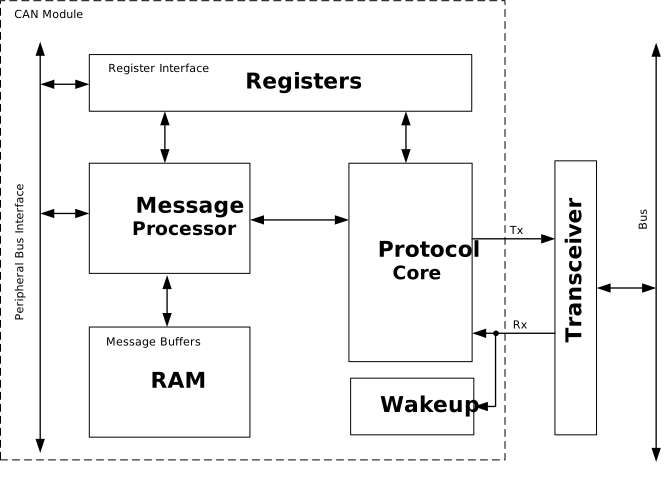
CAN 控制器架构框图
协议核心:负责执行完整的 CAN 底层协议逻辑,包括位时序控制、帧的解析与组装、时钟分频以及采样机制。协议核心通过专用的数据与控制接口,与报文处理器(Message Processor)进行交互,完成报文的实际发送与接收。
报文处理器:负责报文的收发调度与存储管理。当 APB 总线与协议核心同时访问 RAM 时,报文处理器执行仲裁以确保数据一致性;在接收方向,扫描 RAM 空间为接收报文分配存储位置;在发送方向,根据优先级决定下一条待发送报文。此外,报文处理器还支持对远程帧进行硬件自动回复或保存处理。
报文缓冲区:专用的内部 SRAM 空间,由报文处理器统一调度,用于缓冲和存储待发送与已接收的报文。每个 CAN 模块包含 16 个可独立配置的报文缓冲区。
唤醒电路:负责总线唤醒功能。在低功耗模式下,持续监测 Rx 引脚,一旦检测到低电平信号持续时间超过预设阈值,即触发唤醒信号以恢复 CAN 模块及整个系统的工作状态。
寄存器接口:CPU 通过该接口访问 CAN 模块的内部控制与状态寄存器,完成模块配置、状态查询及中断管理等操作。
收发器:通常位于控制器外部,负责将协议核心输出的逻辑电平转换为物理总线所需的差分信号,并将总线差分信号转换为逻辑电平供控制器读取。
功能描述
协议帧格式
根据 ISO 11898-1 标准,CAN 支持四种帧类型:数据帧、远程帧、错误帧和过载帧。此外,帧间空间(Inter-Frame Space)用于分隔连续帧。
数据帧
数据帧用于在节点之间传输数据载荷,是最常用的帧类型。CAN 支持标准数据帧(11 位标识符)和扩展数据帧(29 位标识符)。


数据帧由以下功能段依序组成:
帧起始(SOF):1 位显性电平,标识帧的开始,用于硬同步。
仲裁域:包含标识符(ID)、RTR、IDE 和 SRR 等字段。ID 决定报文优先级,数值越小优先级越高。
控制域:包含数据长度代码(DLC,4 位)和保留位。DLC 指示数据域的字节数(0 ~ 8)。
数据域:有效载荷,0 ~ 8 字节,MSB 先发。
CRC 域:包含 15 位 CRC 序列和 1 位隐性的 CRC 界定符,由硬件自动计算。
ACK 域:发送端输出隐性位,成功接收的节点以显性位应答。
帧结束(EOF):7 位连续隐性电平,标识帧结束。
远程帧
远程帧用于请求某节点发送数据。其结构与数据帧类似,但 RTR 位为隐性且不包含数据域。远程帧同样支持标准格式和扩展格式。

标准远程帧

扩展远程帧
错误帧
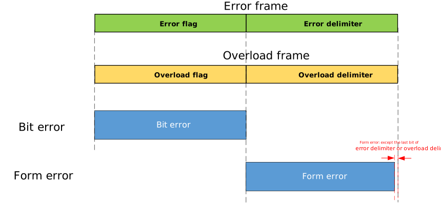
当节点检测到总线错误时发送错误帧,用于破坏当前通信并通知其他节点。错误帧由错误标志(6 位)和错误界定符(8 位隐性)组成,分为两种:
主动错误标志:由处于主动错误状态的节点发送,包含 6 个连续显性位。
被动错误标志:由处于被动错误状态的节点发送,包含 6 个连续隐性位。
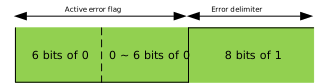
主动错误帧
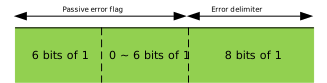
被动错误帧
过载帧
过载帧用于请求额外的帧间延迟。其结构与主动错误帧类似,由过载标志(6 个连续显性位)和过载界定符(8 位隐性)构成。
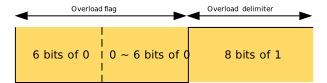
过载帧
帧间空间
ISO 11898-1 标准定义了帧间空间,用于分隔数据帧或远程帧与前面的任何帧。帧间空间由以下阶段组成:
间歇期(Intermission):前一帧的 EOF 或错误/过载界定符结束后,总线必须保持 3 个连续的隐性电平。此期间内任何节点不得发起发送。
挂起(Suspension):处于被动错误状态的节点在作为发送端刚刚发送完一帧报文后,必须在间歇期结束后额外等待 8 个隐性位的时间,才能再次发起下一次发送竞争。主动错误状态的节点无此限制。
总线空闲(Bus Idle):若间歇期和挂起结束后总线上仍无数据传输,总线进入空闲状态,此时任何节点均可发起下一次发送。
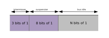
帧间空间
备注
错误帧和过载帧之前不插入帧间空间。
时钟域
每个 CAN 模块有两个时钟域:一个 core_clk 用于处理 CAN 主要功能,另一个低频时钟(OSC4M)用于驱动唤醒电路。 core_clk 时钟域结构如下图所示:
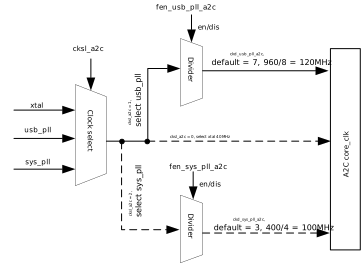
时钟源选择
core_clk 提供三个可选时钟源:
XTAL 40MHz
USB PLL
SYS PLL
时钟源通过 REG_LSYS_CKSL_GRP0 中的 cksl_can 字段选择: cksl_can = 0 选择 XTAL(40 MHz), cksl_can = 1 选择 USB PLL(默认), cksl_can = 3 选择 SYS PLL。
若选择 XTAL(
cksl_can = 0),则直接使用 40 MHz 晶振时钟作为core_clk。若选择 PLL(USB PLL 或 SYS PLL),需额外配置两个参数:
时钟使能(例如 REG_LSYS_CKD_FEN_USB_PLL 中的
fen_usb_pll_can)时钟分频(例如 REG_LSYS_CKD_USB_PLL_GRP0 中的
ckd_usb_pll_can)。
位时序与波特率
当前芯片有两个 CAN 模块,每个 CAN 节点可单独配置位时序参数,最高支持 1 Mbit/s 的通信速率。
位时序分解
根据 ISO 11898-1 标准,一个位时间(Bit Time)分为四段:同步段(Sync_Seg)、传播段(Prop_Seg)、相位缓冲段 1(Phase_Seg1)和相位缓冲段 2(Phase_Seg2):
同步段:固定 1 Tq,期望发生电平跳变的位置,用于同步总线上各节点。
传播段:补偿物理线路上的信号传播延迟及收发器内部硬件延迟。
相位缓冲段 1:采样点前的缓冲段,在重新同步期间可被临时延长。
相位缓冲段 2:采样点后的缓冲段,在重新同步期间可被临时缩短。
时间量子(Time Quantum, Tq)是位时序配置的最小时间单位,所有时间段的长度均以 Tq 为单位配置。Tq 的时长由 core_clk 经波特率预分频器(BRP)分频得到:
Tq = (can_brp + 1) / core_clk
下图展示了一个完整位时间的时序图:
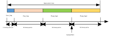
控制器在 Phase_Seg1 与 Phase_Seg2 的交界处对总线电平进行采样(采样点)。通过调整各段长度可控制采样点在位时间中的位置。一个完整的位时间通常由 8 ~ 25 个 Tq 组成。各段的 Tq 分配规则如下:
参数 |
取值范围 |
说明 |
|---|---|---|
预分频器 |
1 ~ 32 |
Tq = (can_brp + 1) / core_clk |
Sync_Seg |
1 Tq(固定) |
同步总线上各节点 |
Prop_Seg |
1 ~ 8 Tq |
补偿网络内的物理延迟 |
Phase_Seg1 |
1 ~ 8 Tq |
补偿边沿相位误差,同步时临时延长 |
Phase_Seg2 |
2 ~ 8 Tq |
补偿边沿相位误差,同步时临时缩短 |
SJW(同步跳转宽度) |
1 ~ 4 Tq |
不得超过 Phase_Seg1 和 Phase_Seg2 中的较小值 |
位时序寄存器配置
位时序参数通过寄存器 CAN_BIT_TIMING 编程。为简化配置,控制器将 Prop_Seg 与 Phase_Seg1 合并为 can_tseg1 ,Phase_Seg2 对应 can_tseg2 。注意 can_brp 、 can_tseg1 和 can_tseg2 为 0 起始的寄存器字段,硬件内部会自动加 1 以获得实际分频值或段长度。字段映射关系如下:
can_brp:预分频器。 实际分频值 =can_brp + 1;Tq = (can_brp + 1) / core_clk。can_tseg1:合并段(Prop_Seg + Phase_Seg1)。实际长度 =can_tseg1 + 1;寄存器值 =Prop_Seg + Phase_Seg1 - 1。can_tseg2:Phase_Seg2。实际长度 =can_tseg2 + 1;寄存器值 =Phase_Seg2 - 1。can_sjw:同步跳转宽度。can_sjw = SJW(直接映射,无偏移)。
波特率计算公式为:
Baud Rate = core_clk / ((can_brp + 1) × (1 + (can_tseg1 + 1) + (can_tseg2 + 1)))
例如, core_clk = 40 MHz、 can_brp = 1 、 can_tseg1 = 14 、 can_tseg2 = 3 时,波特率为 1 Mbit/s:
Baud Rate = 40 / ((1 + 1) × (1 + (14 + 1) + (3 + 1)))
          = 40 / (2 × 20)
          = 1 Mbit/s
采样点位置可通过以下公式计算:
Sample Point = (1 + can_tseg1 + 1) / (1 + (can_tseg1 + 1) + (can_tseg2 + 1))
此配置下采样点位于位时间的 80% 处。
下表列出了 core_clk = 40 MHz 时常用波特率的参考配置:
波特率 |
can_brp |
can_tseg1 |
can_tseg2 |
SJW |
采样点位置 |
|---|---|---|---|---|---|
1 Mbit/s |
1 |
14 |
3 |
1 |
80% |
500 kbit/s |
3 |
14 |
3 |
1 |
80% |
250 kbit/s |
7 |
14 |
3 |
1 |
80% |
125 kbit/s |
15 |
14 |
3 |
1 |
80% |
三点采样模式
将 CAN_CTL 中的 can_tri_sample 设为 1 可启用三点采样模式。在此模式下,控制器在采样点附近对输入信号进行三次采样(各采样点间隔 1 Tq),最终逻辑电平由三次采样值的多数表决结果决定。三点采样模式可有效滤除信号毛刺,提升通信鲁棒性。
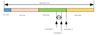
备注
三点采样模式建议在低速率(低于 125 kbit/s)下使用。此时每个 Tq 的时长较长,信号更易受外部干扰产生电平突变,三点采样机制能发挥更好的滤波效果。
工作模式
CAN 模块支持三种工作模式:正常模式、睡眠模式和测试模式。
正常模式
此为默认工作模式。所有子模块(报文处理器、RAM、协议核心和寄存器)协同工作,完成报文收发、错误处理及中断上报。
睡眠模式
在睡眠模式下,大部分子模块被时钟门控,仅唤醒电路保持活动。CAN 无法收发任何帧,模块及系统进入低功耗状态。
睡眠模式通过将 CAN_SLEEP_MODE 中的 can_sleep_en 设为 1 进入。CAN 使用 OSC4M 低频时钟驱动唤醒电路,系统需保持 OSC4M 处于开启状态以支持唤醒监测。
唤醒电路仅在睡眠模式下工作。它通过监测 Rx 引脚上显性电平(低电平)的持续时间,并与预设阈值进行比较:
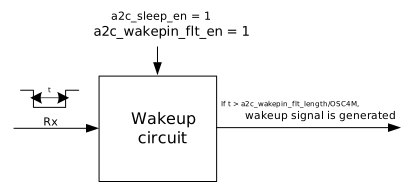
若低电平持续时间超过阈值,触发唤醒信号,重新激活 CAN 模块及整个系统。
若未超过阈值,模块与系统保持睡眠状态。
警告
唤醒操作不关心协议帧的具体内容,触发唤醒的那一帧报文无法被 CAN 接收。后续能否收到数据取决于发送端的重传机制。
唤醒前需确保外部收发器已处于正常工作状态,而非待机或休眠模式。
测试模式
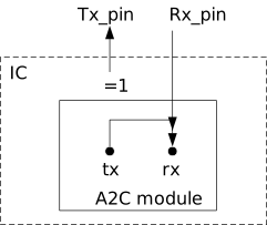
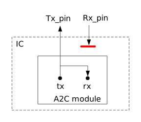
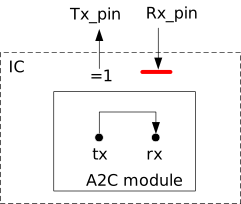
CAN 提供两种测试模式:静默模式和回环模式,主要用于节点自检和总线调试。进入测试模式前,需将 CAN_CTL 中的 test_mode_en 设为 1 启用测试功能,然后通过 CAN_TEST 中的 can_test_cfg 选择具体的测试模式。
报文处理与缓冲区管理
报文处理器(Message Processor)接管报文收发的存储调度以降低 CPU 负载。它在 CPU(APB 总线)和协议核心之间仲裁 RAM 访问,确保数据一致性。
发送方向:根据优先级调度待发送报文。
接收方向:扫描 RAM 并结合过滤与掩码机制为接收报文分配存储空间。
RAM、报文处理器、协议核心和寄存器之间的架构关系如下图所示:
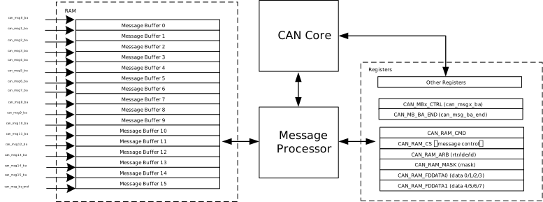
CAN 通过 CAN_RAM_ARB、CAN_RAM_MASK、CAN_RAM_CS、CAN_RAM_DATA 和 CAN_MB_BA_END 等寄存器管理报文缓冲区。
报文缓冲区配置
每个 CAN 模块配备独立的 RAM(352 × 32 位),逻辑上划分为 16 个报文缓冲区(MB0 ~ MB15)。每个缓冲区只能存储一条 CAN 报文,其空间大小可独立配置,默认为 6 × 32 位。
缓冲区基地址通过 CAN_MBx_CTRL 中的 can_msgx_ba 设置(字对齐),RAM 有效地址范围由 CAN_MB_BA_END 中的 can_msg_ba_end 限定。
例如,若 CAN_MB0_CTRL 的 can_msg0_ba 为 0x0,CAN_MB1_CTRL 的 can_msg1_ba 为 0x6,则表示 MB0 分配了 6 × 32 位的存储空间。
接收过滤器
Rx 处理器使用三种接收过滤器对总线上的报文进行硬件级筛选。三种过滤器可灵活组合以满足不同的应用需求。
标识符(ID)过滤器:CAN_RAM_ARB 中的
can_ram_id(29 位)定义期望接收的报文 ID,CAN_RAM_MASK 中的can_ram_id_mask(29 位)为对应掩码:掩码位为 0 表示不比较对应位(即不关心,始终匹配)。
掩码位为 1 表示接收帧中的对应位必须与
can_ram_id严格匹配。
备注
过滤逻辑取决于帧类型:
标准帧(11 位 Base ID):仅比较
can_ram_id的位 [28:18]。扩展帧(29 位 Extended ID):比较
can_ram_id的完整位 [28:0]。
例如,接收标准帧时,若 CAN_RAM_ARB 的位 [28:18] 设为 0x1,CAN_RAM_MASK 的位 [28:18] 设为 0x7FC(低两位掩码为 0),则 Base ID 为 0x00 ~ 0x03 的帧均会被接收。
标识符扩展(IDE)过滤器:CAN_RAM_ARB 中的
can_ram_ide和 CAN_RAM_MASK 中的can_ram_ide_mask控制帧格式过滤:can_ram_ide_mask = 0:不区分帧格式,标准帧和扩展帧均被接收。can_ram_ide_mask = 1:仅接收 IDE 位与can_ram_ide匹配的帧。
can_ram_ide = 0且can_ram_ide_mask = 1:仅接收标准帧。can_ram_ide = 1且can_ram_ide_mask = 1:仅接收扩展帧。
远程传输请求(RTR)过滤器:CAN_RAM_MASK 中的
can_ram_rtr_mask控制帧类型过滤:can_ram_rtr_mask = 0:不区分帧类型,数据帧和远程帧均被接收。can_ram_rtr_mask = 1:仅接收 RTR 位与 CAN_RAM_ARB 中can_ram_rtr匹配的帧。
报文收发流程
发送流程:报文处理器持续扫描 RAM 中所有缓冲区,确定是否有待发送报文,并根据优先级决定发送顺序。当总线处于间歇期、空闲或安全状态时,将选定报文传递至协议核心进行物理发送。CPU 发送报文的配置步骤如下:
在 RAM 接口寄存器中填写发送参数:数据(
can_ram_data)、ID(can_ram_id)和数据长度代码(can_ram_dlc)。设置 RTR 位(
can_ram_rtr)指定帧类型,设置 IDE 位(can_ram_ide)指示帧格式。将 CAN_RAM_CS 中的
can_ram_rxtx设为 1,声明该缓冲区用于发送。向 CAN_RAM_CMD 写入命令以触发传输:设置
can_ram_dir = 1(写操作)、使能can_ram_buffer_en位激活对应缓冲区,然后将can_ram_start设为 1 启动硬件搬运。搬运完成后,can_ram_start由硬件自动清零。此时 CAN_MBx_STS 中对应的
can_msgx_tx_req被置 1,表示报文正在排队等待发送。物理发送成功后该位清零,同时can_msgx_tx_done被置 1。
接收流程:报文通过 CRC 校验后,报文处理器扫描所有接收缓冲区,应用过滤和掩码逻辑寻找匹配的缓冲区。仅在报文无错误接收时,才将其有效载荷存入对应的内部 RAM 位置。CPU 配置接收缓冲区的步骤如下:
在 RAM 接口寄存器中写入期望的 ID(
can_ram_id)和掩码(can_ram_id_mask)。如需精确匹配,CAN_RAM_MASK 中所有相关位应置为 1。根据需求配置 RTR 和 IDE 及其掩码位。
将 CAN_RAM_CS 中的
can_ram_rxtx清零,声明该缓冲区用于接收。向 CAN_RAM_CMD 写入命令完成配置下发。
配置完成后,CAN_MBx_STS 中对应的
can_msgx_rx_rdy被置 1,表示硬件已就绪。当成功匹配并接收到新报文后,can_msgx_rx_vld被置 1,提示 CPU 读取新数据。同时全局状态can_rx_done的对应位也会置起,向 CPU 申请中断(若已使能)。
缓冲区优先级
CAN 控制器提供 16 个报文缓冲区(MB0 ~ MB15),优先级规则如下:
发送优先级(Tx):缓冲区编号升序,编号越小优先级越高。
接收优先级(Rx):缓冲区编号降序,编号越大优先级越高。
此优先级机制完全独立于报文内容,由硬件自动调度。
FIFO 模式
启用 FIFO 功能时,顶部四个报文缓冲区(MB12 ~ MB15)被强制保留用作硬件 FIFO。Rx FIFO 的过滤条件(ID、IDE、RTR 及其掩码)统一继承自 MB12 的配置寄存器,相关的 Rx 中断也基于 MB12 触发。FIFO 在所有 Rx 匹配调度中具有最高优先级。
Rx FIFO 的逻辑框图如下:
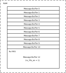
CAN_FIFO_STS 用于监控 FIFO 状态。状态变化过程如下:
默认状态下,FIFO 为空(
fifo_msg_empty = 1)。FIFO 成功接收第一帧时,
fifo_msg_empty变为 0,fifo_msg_lvl递增以指示当前 FIFO 深度。若 FIFO 已存满 4 帧且未被读取,
fifo_msg_full被置 1,此时尚未溢出(fifo_msg_overflow = 0)。若在满载状态下继续接收到匹配的帧,FIFO 执行滚动覆盖策略:最早接收的数据(原 MB12)丢失,原 MB13 的数据移至 MB12,以此类推,新报文存入 MB15。同时触发溢出错误(
fifo_msg_overflow = 1)。
DMA 传输
CAN 模块支持使用 DMA 接收数据,在无需 CPU 干预的情况下,将报文缓冲区的内容(包含仲裁域、控制域及数据域)逐个搬运至目标内存地址。
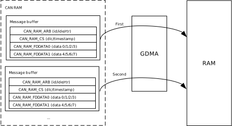
DMA 支持两种流控模式:DMA 作为流控制器,或 CAN 作为流控制器。两种模式的配置步骤完全相同,仅在 CAN_RXDMA_CFG 中的 can_rxdma_owner 字段值不同(0 为 DMA 流控,1 为 CAN 流控)。
DMA 作为流控制器
当 DMA 作为流控制器(Flow Controller)时,传输节拍由 DMA 主导,配置步骤如下:
在 CAN_RXDMA_CFG 中,设置
can_rxdma_owner = 0且can_rxdma_src_msize = 1。在目标报文缓冲区控制寄存器 CAN_MBx_CTRL 中,设置
can_msgx_rxdma_en = 1以使能该缓冲区的 DMA 功能。在 CAN_CTL 中设置
can_rxdma_en = 1,全局使能 CAN 的 DMA 功能。配置 DMA 参数:包括源地址、目的地址、DMA 传输方向、块大小以及源端突发大小(
src_msize)。DMA 中的src_msize必须与 CAN 寄存器中的can_rxdma_src_msize保持一致。
CAN 作为流控制器
当 CAN 充当流控制器主动发起 DMA 请求时,配置步骤如下:
在 CAN_RXDMA_CFG 中,设置
can_rxdma_owner = 1且can_rxdma_src_msize = 1。在目标报文缓冲区控制寄存器 CAN_MBx_CTRL 中,设置
can_msgx_rxdma_en = 1以使能该缓冲区的 DMA 功能。在 CAN_CTL 中设置
can_rxdma_en = 1,全局使能 CAN 的 DMA 功能。配置 DMA 参数。DMA 中的
src_msize必须与 CAN 侧的can_rxdma_src_msize保持一致。
备注
DMA 每次传输仅针对一个报文缓冲区。
DMA 的源端突发大小(
src_msize)必须与 CAN 侧配置的can_rxdma_src_msize保持一致。
错误检测与管理
根据 ISO 11898-1 规范,错误界定(Error Confinement)机制用于实时检测总线通信故障,并通过状态降级限制严重故障节点对总线网络的持续性干扰。
错误界定的整体逻辑框图如下:
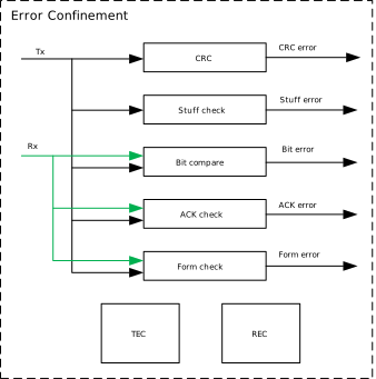
位填充 (Bit Stuffing)
CAN 信号同步依赖于电平跳变沿。若数据流中出现大量连续相同极性的位,接收端将无法维持同步。为此协议引入位填充(Bit Stuffing)机制:
发送端:在 SOF 至 CRC 域之间的字段中,检测到连续 5 个相同极性的位时,自动插入一个极性相反的填充位。
接收端:在 SOF 至 CRC 域之间的字段中,若检测到连续 5 个相同极性的位,则自动剔除随后的相反极性位。若第 6 位的极性与前 5 位相同,则判定为填充错误。
CRC 域之后的界定符、ACK 域和 EOF 等固定格式字段不参与位填充。
错误类型
CAN 支持检测以下五种硬件协议错误:
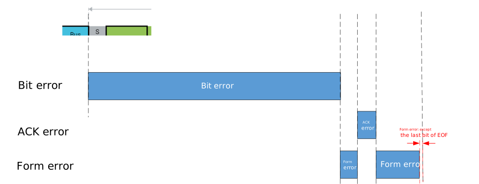
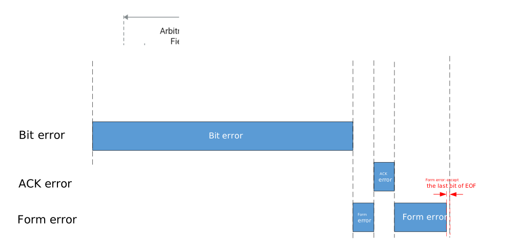
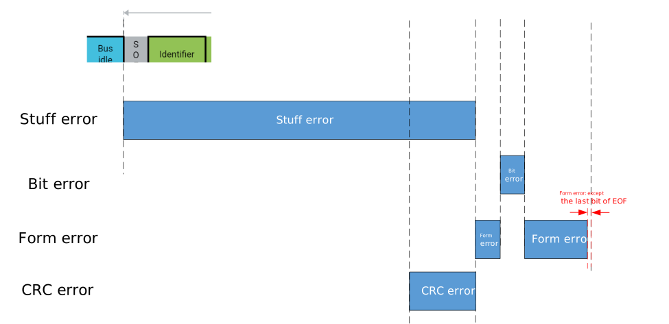
位错误(Bit Error):节点发送位时同步回读总线电平,若回读电平与发送电平不一致(仲裁域或 ACK 域期间受特定规则豁免),则报位错误。
填充错误(Stuff Error):检测到连续 6 个相同极性的位,违反位填充规则。
CRC 错误(CRC Error):接收端计算的 CRC 校验和与报文中 CRC 域的数据不匹配。
格式错误(Form Error):固定格式字段(如 CRC 界定符、ACK 界定符或 EOF)未检测到法定的隐性电平。
ACK 错误(ACK Error):发送节点在 ACK 槽期间未采样到任何接收节点回复的显性 ACK 位。
下表汇总了各类错误的检测范围与错误帧发送时机:
错误种类 |
错误原因 |
检测范围 |
错误帧发送时机 |
检测单元 |
|---|---|---|---|---|
位错误 |
发送电平与回读 电平不一致 |
数据帧/远程帧(SOF ~ CRC), 错误帧/过载帧标志位 |
下一位立即发送 |
发送端 |
填充错误 |
连续 6 个相同 极性的位 |
数据帧/远程帧 (SOF ~ CRC 序列) |
下一位立即发送 |
接收端 |
CRC 错误 |
CRC 校验和 不匹配 |
数据帧/远程帧 (CRC 序列) |
ACK 界定符之后 |
接收端 |
格式错误 |
固定格式字段 未检测到隐性电平 |
数据帧/远程帧(CRC 界定符、 ACK 界定符、EOF 前 6 位), 错误/过载界定符 |
下一位立即发送 (CRC 界定符处视为 CRC 错误,在 ACK 界定符后发送) |
发送端 / 接收端 |
ACK 错误 |
ACK 槽中未检测 到显性电平 |
数据帧/远程帧 (ACK 槽) |
ACK 界定符之后 |
发送端 |
备注
位错误在以下情况下不触发:ID 仲裁阶段发送 1 但回读到 0 时视为仲裁丢失;ACK 槽发送端发出隐性电平且回读仍为隐性时不视为位错误;节点发送被动错误标志期间回读到显性位也不视为位错误。
在 EOF 最后 1 位检测到显性位时,发送过载帧而非错误帧。
错误检测范围
根据 ISO 11898-1 定义,各类错误在报文收发时具有明确的检测区间。
标准数据帧发送时的错误检测范围:
标准远程帧发送时的错误检测范围:
错误帧发送时的错误检测范围:
标准数据帧接收时的错误检测范围:
标准远程帧接收时的错误检测范围:
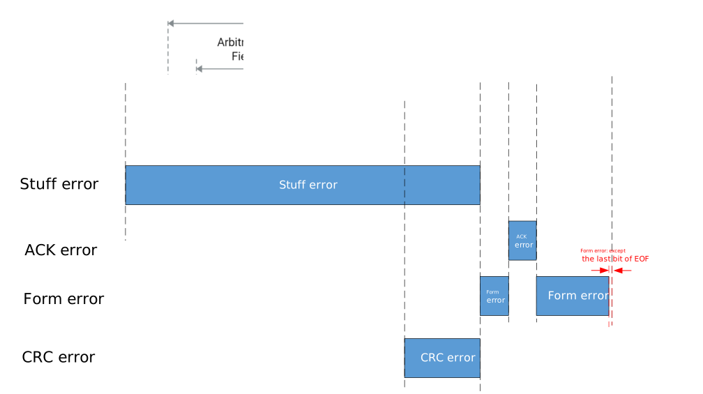
错误帧接收时的错误检测范围:
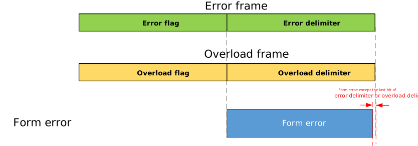
错误状态与计数器
CAN 内部维护两个硬件错误计数器:发送错误计数器(Transmit Error Counter, TEC)和接收错误计数器(Receive Error Counter, REC)。这两个计数器根据协议规则在发生错误或成功收发时动态增减,用于表征当前节点的健康状态。
计数器阈值直接决定节点所处的错误状态,状态转换关系如下图所示:
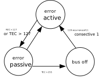
三种错误状态的行为特性如下:
主动错误(error-active):TEC ≤ 127 且 REC ≤ 127。节点正常参与总线通信,检测到错误时立即发送主动错误标志(6 位显性)。
被动错误(error-passive):TEC > 127 或 REC > 127。节点仍可通信,但检测到错误时只发送被动错误标志(6 位隐性),不会干扰其他节点。作为发送端时,连续两帧之间需额外插入 8 个隐性位的挂起时间。
总线关闭(bus-off):TEC > 255。节点被硬件强制从总线断开,无法收发任何数据。
TEC 和 REC 的计数规则如下表所示。计数器变动在检测到错误标志的第一位时触发,一次报文传输可能同时满足多个条件,计数值可能被多次调整。
序号 |
触发条件 |
TEC |
REC |
|---|---|---|---|
1 |
接收端检测到错误(在发送主动错误标志或过载标志期间检测到的位错误除外)。 |
— |
+1 |
2 |
接收端在发送错误标志后,检测到的第一个位为显性位。 |
— |
+8 |
3 |
发送端发送错误标志。 |
+8 |
— |
4 |
发送端在发送主动错误标志或过载标志期间检测到位错误。 |
+8 |
— |
5 |
接收端在发送主动错误标志或过载标志期间检测到位错误。 |
— |
+8 |
6 |
任何节点在发送错误标志或过载标志后,检测到过量的连续显性位:
|
+8 |
+8 |
7 |
发送端成功发送一帧(成功获得 ACK 并且直到 EOF 完成都没有错误)。 |
若 > 0 则 -1; 若 = 0 则不变 |
— |
8 |
接收端成功接收一帧(在 ACK 槽之前无错误,且成功发送显性 ACK 位)。 |
— |
若 1 ≤ REC ≤ 127,则 -1; 若 = 0,则不变; 若 > 127,置为 119 ~ 127 之间 |
9 |
bus-off 恢复(检测到 128 次 × 11 个连续隐性位) |
置 0 |
置 0 |
备注
对于第三项存在例外情况(TEC 保持不变):
发送端处于被动错误状态,因 ACK 槽未检测到显性位产生 ACK 错误,且在发送被动错误标志时未检测到显性位。
发送端因仲裁期间的填充错误发送错误标志(除非该违规位本应是隐性但被监测为显性,此时 TEC 仍增加 8)。
总线关闭与恢复
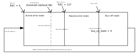
当 TEC 累计超过 255 时,控制器进入 bus-off 状态,节点无法收发任何数据。
恢复条件为:控制器在 bus-off 状态下检测到 128 次 11 个连续隐性位序列(即 128 个总线空闲周期),且软件主动发起恢复请求(写 CAN_CTL 的 CAN_BIT_BUS_ON_REQ 字段)后,硬件执行恢复序列将节点切回主动错误状态。当前状态可通过 CAN_STS 中的 bus_on_state 轮询查询。
总线关闭及恢复机制如下图所示:
错误相关寄存器
CAN 提供以下专用寄存器用于错误诊断与中断管理:
错误状态寄存器 CAN_ERR_STATUS :发生协议错误时,相应位被硬件置 1。若已通过
error_int_en使能对应中断掩码,则向 CPU 产生中断。can_error_rx和can_error_tx字段指示报错瞬间控制器处于接收态还是发送态。错误计数器控制寄存器 CAN_ERR_CNT_CTL :可配置错误警告阈值(
can_error_warn_th)及手动清零计数器(rx_err_cnt_clr和tx_err_cnt_clr)。错误计数器状态寄存器 CAN_ERR_CNT_STS :实时反映
can_rec和can_tec的瞬态值。当
can_rec或can_tec超过 127 时,can_error_passive置 1,模块进入 error-passive 状态。当
can_tec超过 255 时,can_error_busoff置 1,模块进入 bus-off 状态。
寄存器
Base Address:
CAN0_REG : 0x41005000
CAN1_REG : 0x41006000
Name |
Address offset |
Access |
Description |
|---|---|---|---|
000h |
R/W |
Controls the fundamental operations and modes of the CAN bus |
|
004h |
R |
Indicates the overall operational state of the bus |
|
008h |
R |
Monitors the status of the RX FIFO |
|
00Ch |
R/W |
Configures the standard CAN 2.0 bit timing parameters (BRP, SJW, TSEG1, TSEG2) |
|
018h |
R/W |
A global switch to enable or mask various CAN system interrupts |
|
01Ch |
R/W |
Enables or disables receive (RX) interrupts individually for each of the 16 message buffers. |
|
020h |
R/W |
Enables or disables transmit (TX) interrupts individually for each of the 16 message buffers. |
|
024h |
R/W |
Stores the status flags that indicate which specific event (TX, RX, error, etc.) triggered an interrupt. |
|
028h |
R/W |
Provides detailed diagnostics on the type of bus error that occurred |
|
02Ch |
R/W |
Sets the threshold for error warnings and provides a mechanism to clear the internal transmit/receive error counters. |
|
030h |
R |
Displays the current numeric values of the Transmit Error Count (TEC) and Receive Error Count (REC), as well as node states (Warning, Passive, Bus-off) |
|
034h |
R/W |
Flags which specific message buffer encountered an error during its transmission attempt. |
|
038h |
R/W |
Flags which specific message buffer has successfully completed its transmission. |
|
03Ch |
R/W |
Flags which specific message buffer has successfully received a new message. |
|
040h |
R/W |
Manages the internal counter used to apply timestamps to received/transmitted messages, including its prescaler. |
|
044h |
R/W |
Sets up a timer-based trigger mechanism to schedule message transmissions within a specific time window. |
|
048h |
R/W |
Configures how the RX Direct Memory Access (DMA) operates |
|
04Ch |
R |
Acts as the data port from which the DMA controller reads received message payloads. |
|
050h |
R/W |
Manages low-power sleep states, and configures the digital filter for the wakeup pin. |
|
054h |
R/W |
Enables special diagnostic modes, such as silent mode or internal/external loopback testing |
|
100h |
R |
Indicates the individual readiness, validity, and TX/RX status of a specific message buffer. |
|
104h |
R |
Indicates the individual readiness, validity, and TX/RX status of a specific message buffer. |
|
108h |
R |
Indicates the individual readiness, validity, and TX/RX status of a specific message buffer. |
|
10Ch |
R |
Indicates the individual readiness, validity, and TX/RX status of a specific message buffer. |
|
110h |
R |
Indicates the individual readiness, validity, and TX/RX status of a specific message buffer. |
|
114h |
R |
Indicates the individual readiness, validity, and TX/RX status of a specific message buffer. |
|
118h |
R |
Indicates the individual readiness, validity, and TX/RX status of a specific message buffer. |
|
11Ch |
R |
Indicates the individual readiness, validity, and TX/RX status of a specific message buffer. |
|
120h |
R |
Indicates the individual readiness, validity, and TX/RX status of a specific message buffer. |
|
124h |
R |
Indicates the individual readiness, validity, and TX/RX status of a specific message buffer. |
|
128h |
R |
Indicates the individual readiness, validity, and TX/RX status of a specific message buffer. |
|
12Ch |
R |
Indicates the individual readiness, validity, and TX/RX status of a specific message buffer. |
|
130h |
R |
Indicates the individual readiness, validity, and TX/RX status of a specific message buffer. |
|
134h |
R |
Indicates the individual readiness, validity, and TX/RX status of a specific message buffer. |
|
138h |
R |
Indicates the individual readiness, validity, and TX/RX status of a specific message buffer. |
|
13Ch |
R |
Indicates the individual readiness, validity, and TX/RX status of a specific message buffer. |
|
200h |
R/W |
Configures the starting address in RAM and enables DMA functionality for a specific message buffer. |
|
204h |
R/W |
Configures the starting address in RAM and enables DMA functionality for a specific message buffer. |
|
208h |
R/W |
Configures the starting address in RAM and enables DMA functionality for a specific message buffer. |
|
20Ch |
R/W |
Configures the starting address in RAM and enables DMA functionality for a specific message buffer. |
|
210h |
R/W |
Configures the starting address in RAM and enables DMA functionality for a specific message buffer. |
|
214h |
R/W |
Configures the starting address in RAM and enables DMA functionality for a specific message buffer. |
|
218h |
R/W |
Configures the starting address in RAM and enables DMA functionality for a specific message buffer. |
|
21Ch |
R/W |
Configures the starting address in RAM and enables DMA functionality for a specific message buffer. |
|
220h |
R/W |
Configures the starting address in RAM and enables DMA functionality for a specific message buffer. |
|
224h |
R/W |
Configures the starting address in RAM and enables DMA functionality for a specific message buffer. |
|
228h |
R/W |
Configures the starting address in RAM and enables DMA functionality for a specific message buffer. |
|
22Ch |
R/W |
Configures the starting address in RAM and enables DMA functionality for a specific message buffer. |
|
230h |
R/W |
Configures the starting address in RAM and enables DMA functionality for a specific message buffer. |
|
234h |
R/W |
Configures the starting address in RAM and enables DMA functionality for a specific message buffer. |
|
238h |
R/W |
Configures the starting address in RAM and enables DMA functionality for a specific message buffer. |
|
23Ch |
R/W |
Configures the starting address in RAM and enables DMA functionality for a specific message buffer. |
|
2F0h |
R/W |
Defines the ending boundary address in RAM allocated for message buffers. |
|
300h |
R/W |
Serves as the register interface to read or write the actual data payload (up to 64 bytes) into the RAM. |
|
304h |
R/W |
Serves as the register interface to read or write the actual data payload (up to 64 bytes) into the RAM. |
|
308h |
R/W |
Serves as the register interface to read or write the actual data payload (up to 64 bytes) into the RAM. |
|
30Ch |
R/W |
Serves as the register interface to read or write the actual data payload (up to 64 bytes) into the RAM. |
|
310h |
R/W |
Serves as the register interface to read or write the actual data payload (up to 64 bytes) into the RAM. |
|
314h |
R/W |
Serves as the register interface to read or write the actual data payload (up to 64 bytes) into the RAM. |
|
318h |
R/W |
Serves as the register interface to read or write the actual data payload (up to 64 bytes) into the RAM. |
|
31Ch |
R/W |
Serves as the register interface to read or write the actual data payload (up to 64 bytes) into the RAM. |
|
320h |
R/W |
Serves as the register interface to read or write the actual data payload (up to 64 bytes) into the RAM. |
|
324h |
R/W |
Serves as the register interface to read or write the actual data payload (up to 64 bytes) into the RAM. |
|
328h |
R/W |
Serves as the register interface to read or write the actual data payload (up to 64 bytes) into the RAM. |
|
32Ch |
R/W |
Serves as the register interface to read or write the actual data payload (up to 64 bytes) into the RAM. |
|
330h |
R/W |
Serves as the register interface to read or write the actual data payload (up to 64 bytes) into the RAM. |
|
334h |
R/W |
Serves as the register interface to read or write the actual data payload (up to 64 bytes) into the RAM. |
|
338h |
R/W |
Serves as the register interface to read or write the actual data payload (up to 64 bytes) into the RAM. |
|
33Ch |
R/W |
Serves as the register interface to read or write the actual data payload (up to 64 bytes) into the RAM. |
|
340h |
R/W |
Configures the message identifier (ID), format (IDE), and frame type (RTR) for a message buffer being written to or read from RAM. |
|
344h |
R/W |
Configures the acceptance filter masks, defining which bits of an incoming message ID must match to be accepted into the buffer. |
|
348h |
R/W |
Configures control and status attributes of the message, such as Data Length Code (DLC) and direction (TX/RX). |
|
34Ch |
R/W |
Executes the command to transfer data between the CAN_RAM_* registers and the actual internal SRAM for a specified message buffer. |
|
3F8h |
R/W |
Selects and enables internal hardware signals to be routed to debug pins for hardware troubleshooting. |
|
3FCh |
R/W |
A reserved placeholder register used for hardware alignment or future expansion. |
REG_CAN_CTL
Name: CAN bus control register
Size: 32
Address offset: 000h
Read/write access: R/W
Controls the fundamental operations and modes of the CAN bus
Bit |
Symbol |
Access |
INI |
Description |
|---|---|---|---|---|
31:8 |
RSVD |
R |
- |
Reserved |
7 |
CAN_RXDMA_EN |
R/W |
0x0 |
Rx dma enable |
6 |
RSVD |
R |
- |
Reserved |
5 |
RX_FIFO_EN |
R/W |
0x0 |
Rx fifo function enable |
4 |
TEST_MODE_EN |
R/W |
0x0 |
Test mode enable, for lbk or silent mode use |
3 |
AUTO_RE_TX_EN |
R/W |
0x0 |
Auto re-transmission enabled |
2 |
CAN_TRI_SAMPLE |
R/W |
0x0 |
Triple sample mode |
1 |
BUS_ON_REQ |
R/W |
0x0 |
Request to bus_on |
0 |
CAN_EN |
R/W |
0x0 |
Can enable |
REG_CAN_STS
Name: CAN bus status
Size: 32
Address offset: 004h
Read/write access: R
Indicates the overall operational state of the bus
Bit |
Symbol |
Access |
INI |
Description |
|---|---|---|---|---|
31:1 |
RSVD |
R |
- |
Reserved |
0 |
BUS_ON_STATE |
R |
0x0 |
Bus state
|
REG_CAN_FIFO_STS
Name: CAN bus FIFO status
Size: 32
Address offset: 008h
Read/write access: R
Monitors the status of the RX FIFO
Bit |
Symbol |
Access |
INI |
Description |
|---|---|---|---|---|
31:7 |
RSVD |
R |
- |
Reserved |
6:4 |
FIFO_MSG_LVL |
R |
0x0 |
Rx fifo message level |
3 |
RSVD |
R |
- |
Reserved |
2 |
FIFO_MSG_OVERFLOW |
R |
0x0 |
Rx fifo overflow |
1 |
FIFO_MSG_EMPTY |
R |
0x1 |
Rx fifo empty |
0 |
FIFO_MSG_FULL |
R |
0x0 |
Rx fifo full |
REG_CAN_BIT_TIMING
Name: CAN2.0 bit timing
Size: 32
Address offset: 00Ch
Read/write access: R/W
Configures the standard CAN 2.0 bit timing parameters (BRP, SJW, TSEG1, TSEG2)
Bit |
Symbol |
Access |
INI |
Description |
|---|---|---|---|---|
31:24 |
CAN_BRP |
R/W |
0x0 |
CAN bit timing perscaler = <$bit:can_brp>+1 |
23:19 |
RSVD |
R |
- |
Reserved |
18:16 |
CAN_SJW |
R/W |
0x0 |
SJW length = <$bit:can_sjw> |
15:8 |
CAN_TSEG2 |
R/W |
0x0 |
TSEG2 length = <$bit:can_tseg2+1> |
7:0 |
CAN_TSEG1 |
R/W |
0x0 |
TSEG1 length = <$bit:can_tseg1+1> |
REG_CAN_INT_EN
Name: CAN interrupt control
Size: 32
Address offset: 018h
Read/write access: R/W
A global switch to enable or mask various CAN system interrupts
Bit |
Symbol |
Access |
INI |
Description |
|---|---|---|---|---|
31:22 |
RSVD |
R |
- |
Reserved |
21 |
RAM_MOVE_DONE_INT_MASK |
R/W |
0x0 |
Ram move done interrupt mask
|
20 |
BUSOFF_INT_MASK |
R/W |
0x0 |
Wakeup interrupt mask
|
19 |
WAKEUP_INT_MASK |
R/W |
0x0 |
Wakeup interrupt mask
|
18 |
ERROR_INT_MASK |
R/W |
0x0 |
Error interrupt mask
|
17 |
RX_INT_MASK |
R/W |
0x0 |
Rx interrupt mask
|
16 |
TX_INT_MASK |
R/W |
0x0 |
Tx interrupt mask
|
15:6 |
RSVD |
R |
- |
Reserved |
5 |
RAM_MOVE_DONE_INT_EN |
R/W |
0x0 |
Ram move done interrupt enable |
4 |
BUSOFF_INT_EN |
R/W |
0x0 |
Wakeup interrupt enbale |
3 |
WAKEUP_INT_EN |
R/W |
0x0 |
Wakeup interrupt enbale |
2 |
ERROR_INT_EN |
R/W |
0x0 |
Error interrupt enable |
1 |
RX_INT_EN |
R/W |
0x0 |
Rx interrupt enable |
0 |
TX_INT_EN |
R/W |
0x0 |
Tx interrupt enable |
REG_CAN_MB_RXINT_EN
Name: CAN rx interrupt for message buffers
Size: 32
Address offset: 01Ch
Read/write access: R/W
Enables or disables receive (RX) interrupts individually for each of the 16 message buffers.
Bit |
Symbol |
Access |
INI |
Description |
|---|---|---|---|---|
31:16 |
RSVD |
R |
- |
Reserved |
15:0 |
CAN_MB_RXINT_EN |
R/W |
0x0 |
Rx interrupt enable for each message buffer |
REG_CAN_MB_TXINT_EN
Name: CAN tx interrupt for message buffers
Size: 32
Address offset: 020h
Read/write access: R/W
Enables or disables transmit (TX) interrupts individually for each of the 16 message buffers.
Bit |
Symbol |
Access |
INI |
Description |
|---|---|---|---|---|
31:16 |
RSVD |
R |
- |
Reserved |
15:0 |
CAN_MB_TXINT_EN |
R/W |
0x0 |
Tx interrupt enable for each message buffer |
REG_CAN_INT_FLAG
Name: CAN interrupt flags
Size: 32
Address offset: 024h
Read/write access: R/W
Stores the status flags that indicate which specific event (TX, RX, error, etc.) triggered an
interrupt.
Bit |
Symbol |
Access |
INI |
Description |
|---|---|---|---|---|
31:6 |
RSVD |
R |
- |
Reserved |
5 |
RAM_MOVE_DONE_INT_FLAG |
R/W |
0x0 |
Data move from register to CAN IP internal RAM finished interupt, move from RAM to register done will NOT generate interrupt, write one to clear |
4 |
BUSOFF_INT_FLAG |
R/W |
0x0 |
Busoff interrupt flag, write one to clear |
3 |
WAKEUP_INT_FLAG |
R/W |
0x0 |
Wakeup interrupt flag, write one to clear |
2 |
ERROR_INT_FLAG |
R/W |
0x0 |
Error interrupt flag, write to clear |
1 |
RX_INT_FLAG |
R/W |
0x0 |
Rx interrupt flag, write to clear |
0 |
TX_INT_FLAG |
R/W |
0x0 |
Tx interrupt flag, write to clear |
REG_CAN_ERR_STATUS
Name: CAN error status
Size: 32
Address offset: 028h
Read/write access: R/W
Provides detailed diagnostics on the type of bus error that occurred
Bit |
Symbol |
Access |
INI |
Description |
|---|---|---|---|---|
31:10 |
RSVD |
R |
- |
Reserved |
9 |
CAN_ERROR_RX |
R/W |
0x0 |
Can rx error flag |
8 |
CAN_ERROR_TX |
R/W |
0x0 |
Can tx error flag |
7:6 |
RSVD |
R |
- |
Reserved |
5 |
CAN_ERROR_ACK |
R/W |
0x0 |
Latest error is ack error |
4 |
CAN_ERROR_STUFF |
R/W |
0x0 |
Latest error is stuff error |
3 |
CAN_ERROR_CRC |
R/W |
0x0 |
Latest error is ctc error |
2 |
CAN_ERROR_FORM |
R/W |
0x0 |
Latest error is form error |
1 |
CAN_ERROR_BIT1 |
R/W |
0x0 |
Latest error is bit1 error, tx=1 but rx=0 |
0 |
CAN_ERROR_BIT0 |
R/W |
0x0 |
Latest error is bit0 error, tx=0 but rx=1 |
REG_CAN_ERR_CNT_CTL
Name: CAN bus error counter control
Size: 32
Address offset: 02Ch
Read/write access: R/W
Sets the threshold for error warnings and provides a mechanism to clear the internal
transmit/receive error counters.
Bit |
Symbol |
Access |
INI |
Description |
|---|---|---|---|---|
31:17 |
RSVD |
R |
- |
Reserved |
16:8 |
CAN_ERROR_WARN_TH |
R/W |
0x60 |
Error counter warning threshold, programable, default 96. NOTES: 0~127 is availaible to both TEC and REC, 128~255 is only available to TEC |
7:2 |
RSVD |
R |
- |
Reserved |
1 |
RX_ERR_CNT_CLR |
R/W |
0x0 |
Write 1 to clear can_rec |
0 |
TX_ERR_CNT_CLR |
R/W |
0x0 |
Write 1 to clear can_tec |
REG_CAN_ERR_CNT_STS
Name: CAN bus error counter status
Size: 32
Address offset: 030h
Read/write access: R
Displays the current numeric values of the Transmit Error Count (TEC) and Receive Error Count (REC),
as well as node states (Warning, Passive, Bus-off)
Bit |
Symbol |
Access |
INI |
Description |
|---|---|---|---|---|
31 |
RSVD |
R |
- |
Reserved |
30 |
CAN_ERROR_WARNING |
R |
0x0 |
Error counter arrive at warning threshold |
29 |
CAN_ERROR_BUSOFF |
R |
0x0 |
Error counter arrive at bus off level |
28 |
CAN_ERROR_PASSIVE |
R |
0x0 |
Error counter arrive at error passive level |
27:25 |
RSVD |
R |
- |
Reserved |
24:16 |
CAN_REC |
R |
0x0 |
Receive error count |
15:9 |
RSVD |
R |
- |
Reserved |
8:0 |
CAN_TEC |
R |
0x0 |
Transmit error count |
REG_CAN_TX_ERROR_FLAG
Name: CAN tx error flag for each message buffe
Size: 32
Address offset: 034h
Read/write access: R/W
Flags which specific message buffer encountered an error during its transmission attempt.
Bit |
Symbol |
Access |
INI |
Description |
|---|---|---|---|---|
31:16 |
RSVD |
R |
- |
Reserved |
15:0 |
CAN_TX_ERROR_FLAG |
R/W |
0x0 |
Indicate which message tx buffer have error detected, cpu can write 1 to clear |
REG_CAN_TX_DONE
Name: CAN tx done for message buffers
Size: 32
Address offset: 038h
Read/write access: R/W
Flags which specific message buffer has successfully completed its transmission.
Bit |
Symbol |
Access |
INI |
Description |
|---|---|---|---|---|
31:16 |
RSVD |
R |
- |
Reserved |
15:0 |
CAN_TX_DONE |
R/W |
0x0 |
Tx done for each message buffer |
REG_CAN_RX_DONE
Name: CAN rx done for message buffers
Size: 32
Address offset: 03Ch
Read/write access: R/W
Flags which specific message buffer has successfully received a new message.
Bit |
Symbol |
Access |
INI |
Description |
|---|---|---|---|---|
31:16 |
RSVD |
R |
- |
Reserved |
15:0 |
CAN_RX_DONE |
R/W |
0x0 |
Rx done for each message buffer |
REG_CAN_TIME_STAMP
Name: Timestamp function
Size: 32
Address offset: 040h
Read/write access: R/W
Manages the internal counter used to apply timestamps to received/transmitted messages, including
its prescaler.
Bit |
Symbol |
Access |
INI |
Description |
|---|---|---|---|---|
31 |
CAN_TIME_STAMP_EN |
R/W |
0x0 |
Time stamp function enable and time stamp counter start |
30:24 |
RSVD |
R |
- |
Reserved |
23:16 |
CAN_TIME_STAMP_DIV |
R/W |
0x0 |
Timer stamp conter prescalar |
15:0 |
CAN_TIME_STAMP |
R |
0x0 |
Time stamp counter value, up count |
REG_CAN_MB_TRIGGER
Name: CAN tx trigger by timer configuration
Size: 32
Address offset: 044h
Read/write access: R/W
Sets up a timer-based trigger mechanism to schedule message transmissions within a specific time
window.
Bit |
Symbol |
Access |
INI |
Description |
|---|---|---|---|---|
31:25 |
RSVD |
R |
- |
Reserved |
24 |
TX_TRIGGER_EN |
R/W |
0x0 |
End of message buffer base address in RAM |
23:16 |
TX_TRIGGER_CLOSE_OFFSET |
R/W |
0x0 |
End of trigger time = <$bit:tx_trigger_begin> + <$bit:tx_trigger_close_offset> |
15:0 |
TX_TRIGGER_BEGIN |
R/W |
0x0 |
Start of trigger time |
REG_CAN_RXDMA_CFG
Name: RX dma configuration
Size: 32
Address offset: 048h
Read/write access: R/W
Configures how the RX Direct Memory Access (DMA) operates
Bit |
Symbol |
Access |
INI |
Description |
|---|---|---|---|---|
31:25 |
RSVD |
R |
- |
Reserved |
24 |
CAN_RXDMA_OWNER |
R/W |
0x0 |
Can rxdma owner is :
|
23:18 |
RSVD |
R |
- |
Reserved |
17:16 |
CAN_RXDMA_SRC_MSIZE |
R/W |
0x1 |
Rx dma burst size:
|
15:14 |
RSVD |
R |
- |
Reserved |
13:0 |
CAN_RXDMA_FRAME_SIZE |
R |
0x2 |
Can rx dma data frame size = ceil(<rx_dma_data bytes number>/4 ), for example: rx_dma_data is 9~12 bytes, frame size is 3 |
REG_CAN_RX_DMA_DATA
Name: Register for dma access message buffe
Size: 32
Address offset: 04Ch
Read/write access: R
Acts as the data port from which the DMA controller reads received message payloads.
Bit |
Symbol |
Access |
INI |
Description |
|---|---|---|---|---|
31:0 |
CAN_RX_DMA_DATA |
R |
0x0 |
For DMA read received data |
REG_CAN_SLEEP_MODE
Name: sleep mode request and wakeup pin digital filter
Size: 32
Address offset: 050h
Read/write access: R/W
Manages low-power sleep states, and configures the digital filter for the wakeup pin.
Bit |
Symbol |
Access |
INI |
Description |
|---|---|---|---|---|
31:18 |
RSVD |
R |
- |
Reserved |
17 |
CAN_SLEEP_STATE |
R |
0x0 |
Can is sleep or not
|
16 |
CAN_SLEEP_EN |
R/W |
0x0 |
Can sleep enable
|
15:9 |
RSVD |
R |
- |
Reserved |
8 |
CAN_WAKEPIN_FLT_EN |
R/W |
0x0 |
Wakeup pin digital filter enable |
7:0 |
CAN_WAKEPIN_FLT_LENGTH |
R/W |
0x1 |
Wakeup pin digital filter length |
REG_CAN_TEST
Name: test configuration
Size: 32
Address offset: 054h
Read/write access: R/W
Enables special diagnostic modes, such as silent mode or internal/external loopback testing
Bit |
Symbol |
Access |
INI |
Description |
|---|---|---|---|---|
31:2 |
RSVD |
R |
- |
Reserved |
1:0 |
CAN_TEST_CFG |
R/W |
0x0 |
|
REG_CAN_MB0_STS
Size: 32
Address offset: 100h
Read/write access: R
Indicates the individual readiness, validity, and TX/RX status of a specific message buffer.
Bit |
Symbol |
Access |
INI |
Description |
|---|---|---|---|---|
31:4 |
RSVD |
R |
- |
Reserved |
3 |
CAN_MSG0_RX_VLD |
R |
0x0 |
New message have been received in the message buffer |
2 |
CAN_MSG0_RX_RDY |
R |
0x0 |
The message buffer is ready for receiving a new message |
1 |
CAN_MSG0_TX_DONE |
R |
0x0 |
Tx message in the message buffer finish sending |
0 |
CAN_MSG0_TX_REQ |
R |
0x0 |
Tx message is pending for transmit |
REG_CAN_MB1_STS
Size: 32
Address offset: 104h
Read/write access: R
Indicates the individual readiness, validity, and TX/RX status of a specific message buffer.
Bit |
Symbol |
Access |
INI |
Description |
|---|---|---|---|---|
31:4 |
RSVD |
R |
- |
Reserved |
3 |
CAN_MSG1_RX_VLD |
R |
0x0 |
New message have been received in the message buffer |
2 |
CAN_MSG1_RX_RDY |
R |
0x0 |
The message buffer is ready for receiving a new message |
1 |
CAN_MSG1_TX_DONE |
R |
0x0 |
Tx message in the message buffer finish sending |
0 |
CAN_MSG1_TX_REQ |
R |
0x0 |
Tx message is pending for transmit |
REG_CAN_MB2_STS
Size: 32
Address offset: 108h
Read/write access: R
Indicates the individual readiness, validity, and TX/RX status of a specific message buffer.
Bit |
Symbol |
Access |
INI |
Description |
|---|---|---|---|---|
31:4 |
RSVD |
R |
- |
Reserved |
3 |
CAN_MSG2_RX_VLD |
R |
0x0 |
New message have been received in the message buffer |
2 |
CAN_MSG2_RX_RDY |
R |
0x0 |
The message buffer is ready for receiving a new message |
1 |
CAN_MSG2_TX_DONE |
R |
0x0 |
Tx message in the message buffer finish sending |
0 |
CAN_MSG2_TX_REQ |
R |
0x0 |
Tx message is pending for transmit |
REG_CAN_MB3_STS
Size: 32
Address offset: 10Ch
Read/write access: R
Indicates the individual readiness, validity, and TX/RX status of a specific message buffer.
Bit |
Symbol |
Access |
INI |
Description |
|---|---|---|---|---|
31:4 |
RSVD |
R |
- |
Reserved |
3 |
CAN_MSG3_RX_VLD |
R |
0x0 |
New message have been received in the message buffer |
2 |
CAN_MSG3_RX_RDY |
R |
0x0 |
The message buffer is ready for receiving a new message |
1 |
CAN_MSG3_TX_DONE |
R |
0x0 |
Tx message in the message buffer finish sending |
0 |
CAN_MSG3_TX_REQ |
R |
0x0 |
Tx message is pending for transmit |
REG_CAN_MB4_STS
Size: 32
Address offset: 110h
Read/write access: R
Indicates the individual readiness, validity, and TX/RX status of a specific message buffer.
Bit |
Symbol |
Access |
INI |
Description |
|---|---|---|---|---|
31:4 |
RSVD |
R |
- |
Reserved |
3 |
CAN_MSG4_RX_VLD |
R |
0x0 |
New message have been received in the message buffer |
2 |
CAN_MSG4_RX_RDY |
R |
0x0 |
The message buffer is ready for receiving a new message |
1 |
CAN_MSG4_TX_DONE |
R |
0x0 |
Tx message in the message buffer finish sending |
0 |
CAN_MSG4_TX_REQ |
R |
0x0 |
Tx message is pending for transmit |
REG_CAN_MB5_STS
Size: 32
Address offset: 114h
Read/write access: R
Indicates the individual readiness, validity, and TX/RX status of a specific message buffer.
Bit |
Symbol |
Access |
INI |
Description |
|---|---|---|---|---|
31:4 |
RSVD |
R |
- |
Reserved |
3 |
CAN_MSG5_RX_VLD |
R |
0x0 |
New message have been received in the message buffer |
2 |
CAN_MSG5_RX_RDY |
R |
0x0 |
The message buffer is ready for receiving a new message |
1 |
CAN_MSG5_TX_DONE |
R |
0x0 |
Tx message in the message buffer finish sending |
0 |
CAN_MSG5_TX_REQ |
R |
0x0 |
Tx message is pending for transmit |
REG_CAN_MB6_STS
Size: 32
Address offset: 118h
Read/write access: R
Indicates the individual readiness, validity, and TX/RX status of a specific message buffer.
Bit |
Symbol |
Access |
INI |
Description |
|---|---|---|---|---|
31:4 |
RSVD |
R |
- |
Reserved |
3 |
CAN_MSG6_RX_VLD |
R |
0x0 |
New message have been received in the message buffer |
2 |
CAN_MSG6_RX_RDY |
R |
0x0 |
The message buffer is ready for receiving a new message |
1 |
CAN_MSG6_TX_DONE |
R |
0x0 |
Tx message in the message buffer finish sending |
0 |
CAN_MSG6_TX_REQ |
R |
0x0 |
Tx message is pending for transmit |
REG_CAN_MB7_STS
Size: 32
Address offset: 11Ch
Read/write access: R
Indicates the individual readiness, validity, and TX/RX status of a specific message buffer.
Bit |
Symbol |
Access |
INI |
Description |
|---|---|---|---|---|
31:4 |
RSVD |
R |
- |
Reserved |
3 |
CAN_MSG7_RX_VLD |
R |
0x0 |
New message have been received in the message buffer |
2 |
CAN_MSG7_RX_RDY |
R |
0x0 |
The message buffer is ready for receiving a new message |
1 |
CAN_MSG7_TX_DONE |
R |
0x0 |
Tx message in the message buffer finish sending |
0 |
CAN_MSG7_TX_REQ |
R |
0x0 |
Tx message is pending for transmit |
REG_CAN_MB8_STS
Size: 32
Address offset: 120h
Read/write access: R
Indicates the individual readiness, validity, and TX/RX status of a specific message buffer.
Bit |
Symbol |
Access |
INI |
Description |
|---|---|---|---|---|
31:4 |
RSVD |
R |
- |
Reserved |
3 |
CAN_MSG8_RX_VLD |
R |
0x0 |
New message have been received in the message buffer |
2 |
CAN_MSG8_RX_RDY |
R |
0x0 |
The message buffer is ready for receiving a new message |
1 |
CAN_MSG8_TX_DONE |
R |
0x0 |
Tx message in the message buffer finish sending |
0 |
CAN_MSG8_TX_REQ |
R |
0x0 |
Tx message is pending for transmit |
REG_CAN_MB9_STS
Size: 32
Address offset: 124h
Read/write access: R
Indicates the individual readiness, validity, and TX/RX status of a specific message buffer.
Bit |
Symbol |
Access |
INI |
Description |
|---|---|---|---|---|
31:4 |
RSVD |
R |
- |
Reserved |
3 |
CAN_MSG9_RX_VLD |
R |
0x0 |
New message have been received in the message buffer |
2 |
CAN_MSG9_RX_RDY |
R |
0x0 |
The message buffer is ready for receiving a new message |
1 |
CAN_MSG9_TX_DONE |
R |
0x0 |
Tx message in the message buffer finish sending |
0 |
CAN_MSG9_TX_REQ |
R |
0x0 |
Tx message is pending for transmit |
REG_CAN_MB10_STS
Size: 32
Address offset: 128h
Read/write access: R
Indicates the individual readiness, validity, and TX/RX status of a specific message buffer.
Bit |
Symbol |
Access |
INI |
Description |
|---|---|---|---|---|
31:4 |
RSVD |
R |
- |
Reserved |
3 |
CAN_MSG10_RX_VLD |
R |
0x0 |
New message have been received in the message buffer |
2 |
CAN_MSG10_RX_RDY |
R |
0x0 |
The message buffer is ready for receiving a new message |
1 |
CAN_MSG10_TX_DONE |
R |
0x0 |
Tx message in the message buffer finish sending |
0 |
CAN_MSG10_TX_REQ |
R |
0x0 |
Tx message is pending for transmit |
REG_CAN_MB11_STS
Size: 32
Address offset: 12Ch
Read/write access: R
Indicates the individual readiness, validity, and TX/RX status of a specific message buffer.
Bit |
Symbol |
Access |
INI |
Description |
|---|---|---|---|---|
31:4 |
RSVD |
R |
- |
Reserved |
3 |
CAN_MSG11_RX_VLD |
R |
0x0 |
New message have been received in the message buffer |
2 |
CAN_MSG11_RX_RDY |
R |
0x0 |
The message buffer is ready for receiving a new message |
1 |
CAN_MSG11_TX_DONE |
R |
0x0 |
Tx message in the message buffer finish sending |
0 |
CAN_MSG11_TX_REQ |
R |
0x0 |
Tx message is pending for transmit |
REG_CAN_MB12_STS
Size: 32
Address offset: 130h
Read/write access: R
Indicates the individual readiness, validity, and TX/RX status of a specific message buffer.
Bit |
Symbol |
Access |
INI |
Description |
|---|---|---|---|---|
31:4 |
RSVD |
R |
- |
Reserved |
3 |
CAN_MSG12_RX_VLD |
R |
0x0 |
New message have been received in the message buffer |
2 |
CAN_MSG12_RX_RDY |
R |
0x0 |
The message buffer is ready for receiving a new message |
1 |
CAN_MSG12_TX_DONE |
R |
0x0 |
Tx message in the message buffer finish sending |
0 |
CAN_MSG12_TX_REQ |
R |
0x0 |
Tx message is pending for transmit |
REG_CAN_MB13_STS
Size: 32
Address offset: 134h
Read/write access: R
Indicates the individual readiness, validity, and TX/RX status of a specific message buffer.
Bit |
Symbol |
Access |
INI |
Description |
|---|---|---|---|---|
31:4 |
RSVD |
R |
- |
Reserved |
3 |
CAN_MSG13_RX_VLD |
R |
0x0 |
New message have been received in the message buffer |
2 |
CAN_MSG13_RX_RDY |
R |
0x0 |
The message buffer is ready for receiving a new message |
1 |
CAN_MSG13_TX_DONE |
R |
0x0 |
Tx message in the message buffer finish sending |
0 |
CAN_MSG13_TX_REQ |
R |
0x0 |
Tx message is pending for transmit |
REG_CAN_MB14_STS
Size: 32
Address offset: 138h
Read/write access: R
Indicates the individual readiness, validity, and TX/RX status of a specific message buffer.
Bit |
Symbol |
Access |
INI |
Description |
|---|---|---|---|---|
31:4 |
RSVD |
R |
- |
Reserved |
3 |
CAN_MSG14_RX_VLD |
R |
0x0 |
New message have been received in the message buffer |
2 |
CAN_MSG14_RX_RDY |
R |
0x0 |
The message buffer is ready for receiving a new message |
1 |
CAN_MSG14_TX_DONE |
R |
0x0 |
Tx message in the message buffer finish sending |
0 |
CAN_MSG14_TX_REQ |
R |
0x0 |
Tx message is pending for transmit |
REG_CAN_MB15_STS
Size: 32
Address offset: 13Ch
Read/write access: R
Indicates the individual readiness, validity, and TX/RX status of a specific message buffer.
Bit |
Symbol |
Access |
INI |
Description |
|---|---|---|---|---|
31:4 |
RSVD |
R |
- |
Reserved |
3 |
CAN_MSG15_RX_VLD |
R |
0x0 |
New message have been received in the message buffer |
2 |
CAN_MSG15_RX_RDY |
R |
0x0 |
The message buffer is ready for receiving a new message |
1 |
CAN_MSG15_TX_DONE |
R |
0x0 |
Tx message in the message buffer finish sending |
0 |
CAN_MSG15_TX_REQ |
R |
0x0 |
Tx message is pending for transmit |
REG_CAN_MB0_CTRL
Size: 32
Address offset: 200h
Read/write access: R/W
Configures the starting address in RAM and enables DMA functionality for a specific message buffer.
Bit |
Symbol |
Access |
INI |
Description |
|---|---|---|---|---|
31:25 |
RSVD |
R |
- |
Reserved |
24 |
CAN_MSG0_RXDMA_EN |
R/W |
0x0 |
Dma enable when the message buffer used as rx |
23:9 |
RSVD |
R |
- |
Reserved |
8:0 |
CAN_MSG0_BA |
R/W |
9'd0 |
Message buffer base address in RAM |
REG_CAN_MB1_CTRL
Size: 32
Address offset: 204h
Read/write access: R/W
Configures the starting address in RAM and enables DMA functionality for a specific message buffer.
Bit |
Symbol |
Access |
INI |
Description |
|---|---|---|---|---|
31:25 |
RSVD |
R |
- |
Reserved |
24 |
CAN_MSG1_RXDMA_EN |
R/W |
0x0 |
Dma enable when the message buffer used as rx |
23:9 |
RSVD |
R |
- |
Reserved |
8:0 |
CAN_MSG1_BA |
R/W |
9'd6 |
Message buffer base address in RAM |
REG_CAN_MB2_CTRL
Size: 32
Address offset: 208h
Read/write access: R/W
Configures the starting address in RAM and enables DMA functionality for a specific message buffer.
Bit |
Symbol |
Access |
INI |
Description |
|---|---|---|---|---|
31:25 |
RSVD |
R |
- |
Reserved |
24 |
CAN_MSG2_RXDMA_EN |
R/W |
0x0 |
Dma enable when the message buffer used as rx |
23:9 |
RSVD |
R |
- |
Reserved |
8:0 |
CAN_MSG2_BA |
R/W |
9'd12 |
Message buffer base address in RAM |
REG_CAN_MB3_CTRL
Size: 32
Address offset: 20Ch
Read/write access: R/W
Configures the starting address in RAM and enables DMA functionality for a specific message buffer.
Bit |
Symbol |
Access |
INI |
Description |
|---|---|---|---|---|
31:25 |
RSVD |
R |
- |
Reserved |
24 |
CAN_MSG3_RXDMA_EN |
R/W |
0x0 |
Dma enable when the message buffer used as rx |
23:9 |
RSVD |
R |
- |
Reserved |
8:0 |
CAN_MSG3_BA |
R/W |
9'd18 |
Message buffer base address in RAM |
REG_CAN_MB4_CTRL
Size: 32
Address offset: 210h
Read/write access: R/W
Configures the starting address in RAM and enables DMA functionality for a specific message buffer.
Bit |
Symbol |
Access |
INI |
Description |
|---|---|---|---|---|
31:25 |
RSVD |
R |
- |
Reserved |
24 |
CAN_MSG4_RXDMA_EN |
R/W |
0x0 |
Dma enable when the message buffer used as rx |
23:9 |
RSVD |
R |
- |
Reserved |
8:0 |
CAN_MSG4_BA |
R/W |
9'd24 |
Message buffer base address in RAM |
REG_CAN_MB5_CTRL
Size: 32
Address offset: 214h
Read/write access: R/W
Configures the starting address in RAM and enables DMA functionality for a specific message buffer.
Bit |
Symbol |
Access |
INI |
Description |
|---|---|---|---|---|
31:25 |
RSVD |
R |
- |
Reserved |
24 |
CAN_MSG5_RXDMA_EN |
R/W |
0x0 |
Dma enable when the message buffer used as rx |
23:9 |
RSVD |
R |
- |
Reserved |
8:0 |
CAN_MSG5_BA |
R/W |
9'd30 |
Message buffer base address in RAM |
REG_CAN_MB6_CTRL
Size: 32
Address offset: 218h
Read/write access: R/W
Configures the starting address in RAM and enables DMA functionality for a specific message buffer.
Bit |
Symbol |
Access |
INI |
Description |
|---|---|---|---|---|
31:25 |
RSVD |
R |
- |
Reserved |
24 |
CAN_MSG6_RXDMA_EN |
R/W |
0x0 |
Dma enable when the message buffer used as rx |
23:9 |
RSVD |
R |
- |
Reserved |
8:0 |
CAN_MSG6_BA |
R/W |
9'd36 |
Message buffer base address in RAM |
REG_CAN_MB7_CTRL
Size: 32
Address offset: 21Ch
Read/write access: R/W
Configures the starting address in RAM and enables DMA functionality for a specific message buffer.
Bit |
Symbol |
Access |
INI |
Description |
|---|---|---|---|---|
31:25 |
RSVD |
R |
- |
Reserved |
24 |
CAN_MSG7_RXDMA_EN |
R/W |
0x0 |
Dma enable when the message buffer used as rx |
23:9 |
RSVD |
R |
- |
Reserved |
8:0 |
CAN_MSG7_BA |
R/W |
9'd42 |
Message buffer base address in RAM |
REG_CAN_MB8_CTRL
Size: 32
Address offset: 220h
Read/write access: R/W
Configures the starting address in RAM and enables DMA functionality for a specific message buffer.
Bit |
Symbol |
Access |
INI |
Description |
|---|---|---|---|---|
31:25 |
RSVD |
R |
- |
Reserved |
24 |
CAN_MSG8_RXDMA_EN |
R/W |
0x0 |
Dma enable when the message buffer used as rx |
23:9 |
RSVD |
R |
- |
Reserved |
8:0 |
CAN_MSG8_BA |
R/W |
9'd48 |
Message buffer base address in RAM |
REG_CAN_MB9_CTRL
Size: 32
Address offset: 224h
Read/write access: R/W
Configures the starting address in RAM and enables DMA functionality for a specific message buffer.
Bit |
Symbol |
Access |
INI |
Description |
|---|---|---|---|---|
31:25 |
RSVD |
R |
- |
Reserved |
24 |
CAN_MSG9_RXDMA_EN |
R/W |
0x0 |
Dma enable when the message buffer used as rx |
23:9 |
RSVD |
R |
- |
Reserved |
8:0 |
CAN_MSG9_BA |
R/W |
9'd54 |
Message buffer base address in RAM |
REG_CAN_MB10_CTRL
Size: 32
Address offset: 228h
Read/write access: R/W
Configures the starting address in RAM and enables DMA functionality for a specific message buffer.
Bit |
Symbol |
Access |
INI |
Description |
|---|---|---|---|---|
31:25 |
RSVD |
R |
- |
Reserved |
24 |
CAN_MSG10_RXDMA_EN |
R/W |
0x0 |
Dma enable when the message buffer used as rx |
23:9 |
RSVD |
R |
- |
Reserved |
8:0 |
CAN_MSG10_BA |
R/W |
9'd60 |
Message buffer base address in RAM |
REG_CAN_MB11_CTRL
Size: 32
Address offset: 22Ch
Read/write access: R/W
Configures the starting address in RAM and enables DMA functionality for a specific message buffer.
Bit |
Symbol |
Access |
INI |
Description |
|---|---|---|---|---|
31:25 |
RSVD |
R |
- |
Reserved |
24 |
CAN_MSG11_RXDMA_EN |
R/W |
0x0 |
Dma enable when the message buffer used as rx |
23:9 |
RSVD |
R |
- |
Reserved |
8:0 |
CAN_MSG11_BA |
R/W |
9'd66 |
Message buffer base address in RAM |
REG_CAN_MB12_CTRL
Size: 32
Address offset: 230h
Read/write access: R/W
Configures the starting address in RAM and enables DMA functionality for a specific message buffer.
Bit |
Symbol |
Access |
INI |
Description |
|---|---|---|---|---|
31:25 |
RSVD |
R |
- |
Reserved |
24 |
CAN_MSG12_RXDMA_EN |
R/W |
0x0 |
Dma enable when the message buffer used as rx |
23:9 |
RSVD |
R |
- |
Reserved |
8:0 |
CAN_MSG12_BA |
R/W |
9'd72 |
Message buffer base address in RAM |
REG_CAN_MB13_CTRL
Size: 32
Address offset: 234h
Read/write access: R/W
Configures the starting address in RAM and enables DMA functionality for a specific message buffer.
Bit |
Symbol |
Access |
INI |
Description |
|---|---|---|---|---|
31:25 |
RSVD |
R |
- |
Reserved |
24 |
CAN_MSG13_RXDMA_EN |
R/W |
0x0 |
Dma enable when the message buffer used as rx |
23:9 |
RSVD |
R |
- |
Reserved |
8:0 |
CAN_MSG13_BA |
R/W |
9'd78 |
Message buffer base address in RAM |
REG_CAN_MB14_CTRL
Size: 32
Address offset: 238h
Read/write access: R/W
Configures the starting address in RAM and enables DMA functionality for a specific message buffer.
Bit |
Symbol |
Access |
INI |
Description |
|---|---|---|---|---|
31:25 |
RSVD |
R |
- |
Reserved |
24 |
CAN_MSG14_RXDMA_EN |
R/W |
0x0 |
Dma enable when the message buffer used as rx |
23:9 |
RSVD |
R |
- |
Reserved |
8:0 |
CAN_MSG14_BA |
R/W |
9'd84 |
Message buffer base address in RAM |
REG_CAN_MB15_CTRL
Size: 32
Address offset: 23Ch
Read/write access: R/W
Configures the starting address in RAM and enables DMA functionality for a specific message buffer.
Bit |
Symbol |
Access |
INI |
Description |
|---|---|---|---|---|
31:25 |
RSVD |
R |
- |
Reserved |
24 |
CAN_MSG15_RXDMA_EN |
R/W |
0x0 |
Dma enable when the message buffer used as rx |
23:9 |
RSVD |
R |
- |
Reserved |
8:0 |
CAN_MSG15_BA |
R/W |
9'd90 |
Message buffer base address in RAM |
REG_CAN_MB_BA_END
Size: 32
Address offset: 2F0h
Read/write access: R/W
Defines the ending boundary address in RAM allocated for message buffers.
Bit |
Symbol |
Access |
INI |
Description |
|---|---|---|---|---|
31:10 |
RSVD |
R |
- |
Reserved |
9:0 |
CAN_MSG_BA_END |
R/W |
10'd96 |
End of message buffer base address in RAM |
REG_CAN_RAM_DATA_15
Name: CAN data
Size: 32
Address offset: 300h
Read/write access: R/W
Serves as the register interface to read or write the actual data payload (up to 64 bytes) into the
RAM.
Bit |
Symbol |
Access |
INI |
Description |
|---|---|---|---|---|
31:24 |
CAN_RAM_DATA_15_3 |
R/W |
0x0 |
Data_byte 4*15+3 |
23:16 |
CAN_RAM_DATA_15_2 |
R/W |
0x0 |
Data_byte 4*15+2 |
15:8 |
CAN_RAM_DATA_15_1 |
R/W |
0x0 |
Data_byte 4*15+1 |
7:0 |
CAN_RAM_DATA_15_0 |
R/W |
0x0 |
Data_byte 4*15+0 |
REG_CAN_RAM_DATA_14
Name: CAN data
Size: 32
Address offset: 304h
Read/write access: R/W
Serves as the register interface to read or write the actual data payload (up to 64 bytes) into the
RAM.
Bit |
Symbol |
Access |
INI |
Description |
|---|---|---|---|---|
31:24 |
CAN_RAM_DATA_14_3 |
R/W |
0x0 |
Data_byte 4*14+3 |
23:16 |
CAN_RAM_DATA_14_2 |
R/W |
0x0 |
Data_byte 4*14+2 |
15:8 |
CAN_RAM_DATA_14_1 |
R/W |
0x0 |
Data_byte 4*14+1 |
7:0 |
CAN_RAM_DATA_14_0 |
R/W |
0x0 |
Data_byte 4*14+0 |
REG_CAN_RAM_DATA_13
Name: CAN data
Size: 32
Address offset: 308h
Read/write access: R/W
Serves as the register interface to read or write the actual data payload (up to 64 bytes) into the
RAM.
Bit |
Symbol |
Access |
INI |
Description |
|---|---|---|---|---|
31:24 |
CAN_RAM_DATA_13_3 |
R/W |
0x0 |
Data_byte 4*13+3 |
23:16 |
CAN_RAM_DATA_13_2 |
R/W |
0x0 |
Data_byte 4*13+2 |
15:8 |
CAN_RAM_DATA_13_1 |
R/W |
0x0 |
Data_byte 4*13+1 |
7:0 |
CAN_RAM_DATA_13_0 |
R/W |
0x0 |
Data_byte 4*13+0 |
REG_CAN_RAM_DATA_12
Name: CAN data
Size: 32
Address offset: 30Ch
Read/write access: R/W
Serves as the register interface to read or write the actual data payload (up to 64 bytes) into the
RAM.
Bit |
Symbol |
Access |
INI |
Description |
|---|---|---|---|---|
31:24 |
CAN_RAM_DATA_12_3 |
R/W |
0x0 |
Data_byte 4*12+3 |
23:16 |
CAN_RAM_DATA_12_2 |
R/W |
0x0 |
Data_byte 4*12+2 |
15:8 |
CAN_RAM_DATA_12_1 |
R/W |
0x0 |
Data_byte 4*12+1 |
7:0 |
CAN_RAM_DATA_12_0 |
R/W |
0x0 |
Data_byte 4*12+0 |
REG_CAN_RAM_DATA_11
Name: CAN data
Size: 32
Address offset: 310h
Read/write access: R/W
Serves as the register interface to read or write the actual data payload (up to 64 bytes) into the
RAM.
Bit |
Symbol |
Access |
INI |
Description |
|---|---|---|---|---|
31:24 |
CAN_RAM_DATA_11_3 |
R/W |
0x0 |
Data_byte 4*11+3 |
23:16 |
CAN_RAM_DATA_11_2 |
R/W |
0x0 |
Data_byte 4*11+2 |
15:8 |
CAN_RAM_DATA_11_1 |
R/W |
0x0 |
Data_byte 4*11+1 |
7:0 |
CAN_RAM_DATA_11_0 |
R/W |
0x0 |
Data_byte 4*11+0 |
REG_CAN_RAM_DATA_10
Name: CAN data
Size: 32
Address offset: 314h
Read/write access: R/W
Serves as the register interface to read or write the actual data payload (up to 64 bytes) into the
RAM.
Bit |
Symbol |
Access |
INI |
Description |
|---|---|---|---|---|
31:24 |
CAN_RAM_DATA_10_3 |
R/W |
0x0 |
Data_byte 4*10+3 |
23:16 |
CAN_RAM_DATA_10_2 |
R/W |
0x0 |
Data_byte 4*10+2 |
15:8 |
CAN_RAM_DATA_10_1 |
R/W |
0x0 |
Data_byte 4*10+1 |
7:0 |
CAN_RAM_DATA_10_0 |
R/W |
0x0 |
Data_byte 4*10+0 |
REG_CAN_RAM_DATA_9
Name: CAN data
Size: 32
Address offset: 318h
Read/write access: R/W
Serves as the register interface to read or write the actual data payload (up to 64 bytes) into the
RAM.
Bit |
Symbol |
Access |
INI |
Description |
|---|---|---|---|---|
31:24 |
CAN_RAM_DATA_9_3 |
R/W |
0x0 |
Data_byte 4*9+3 |
23:16 |
CAN_RAM_DATA_9_2 |
R/W |
0x0 |
Data_byte 4*9+2 |
15:8 |
CAN_RAM_DATA_9_1 |
R/W |
0x0 |
Data_byte 4*9+1 |
7:0 |
CAN_RAM_DATA_9_0 |
R/W |
0x0 |
Data_byte 4*9+0 |
REG_CAN_RAM_DATA_8
Name: CAN data
Size: 32
Address offset: 31Ch
Read/write access: R/W
Serves as the register interface to read or write the actual data payload (up to 64 bytes) into the
RAM.
Bit |
Symbol |
Access |
INI |
Description |
|---|---|---|---|---|
31:24 |
CAN_RAM_DATA_8_3 |
R/W |
0x0 |
Data_byte 4*8+3 |
23:16 |
CAN_RAM_DATA_8_2 |
R/W |
0x0 |
Data_byte 4*8+2 |
15:8 |
CAN_RAM_DATA_8_1 |
R/W |
0x0 |
Data_byte 4*8+1 |
7:0 |
CAN_RAM_DATA_8_0 |
R/W |
0x0 |
Data_byte 4*8+0 |
REG_CAN_RAM_DATA_7
Name: CAN data
Size: 32
Address offset: 320h
Read/write access: R/W
Serves as the register interface to read or write the actual data payload (up to 64 bytes) into the
RAM.
Bit |
Symbol |
Access |
INI |
Description |
|---|---|---|---|---|
31:24 |
CAN_RAM_DATA_7_3 |
R/W |
0x0 |
Data_byte 4*7+3 |
23:16 |
CAN_RAM_DATA_7_2 |
R/W |
0x0 |
Data_byte 4*7+2 |
15:8 |
CAN_RAM_DATA_7_1 |
R/W |
0x0 |
Data_byte 4*7+1 |
7:0 |
CAN_RAM_DATA_7_0 |
R/W |
0x0 |
Data_byte 4*7+0 |
REG_CAN_RAM_DATA_6
Name: CAN data
Size: 32
Address offset: 324h
Read/write access: R/W
Serves as the register interface to read or write the actual data payload (up to 64 bytes) into the
RAM.
Bit |
Symbol |
Access |
INI |
Description |
|---|---|---|---|---|
31:24 |
CAN_RAM_DATA_6_3 |
R/W |
0x0 |
Data_byte 4*6+3 |
23:16 |
CAN_RAM_DATA_6_2 |
R/W |
0x0 |
Data_byte 4*6+2 |
15:8 |
CAN_RAM_DATA_6_1 |
R/W |
0x0 |
Data_byte 4*6+1 |
7:0 |
CAN_RAM_DATA_6_0 |
R/W |
0x0 |
Data_byte 4*6+0 |
REG_CAN_RAM_DATA_5
Name: CAN data
Size: 32
Address offset: 328h
Read/write access: R/W
Serves as the register interface to read or write the actual data payload (up to 64 bytes) into the
RAM.
Bit |
Symbol |
Access |
INI |
Description |
|---|---|---|---|---|
31:24 |
CAN_RAM_DATA_5_3 |
R/W |
0x0 |
Data_byte 4*5+3 |
23:16 |
CAN_RAM_DATA_5_2 |
R/W |
0x0 |
Data_byte 4*5+2 |
15:8 |
CAN_RAM_DATA_5_1 |
R/W |
0x0 |
Data_byte 4*5+1 |
7:0 |
CAN_RAM_DATA_5_0 |
R/W |
0x0 |
Data_byte 4*5+0 |
REG_CAN_RAM_DATA_4
Name: CAN data
Size: 32
Address offset: 32Ch
Read/write access: R/W
Serves as the register interface to read or write the actual data payload (up to 64 bytes) into the
RAM.
Bit |
Symbol |
Access |
INI |
Description |
|---|---|---|---|---|
31:24 |
CAN_RAM_DATA_4_3 |
R/W |
0x0 |
Data_byte 4*4+3 |
23:16 |
CAN_RAM_DATA_4_2 |
R/W |
0x0 |
Data_byte 4*4+2 |
15:8 |
CAN_RAM_DATA_4_1 |
R/W |
0x0 |
Data_byte 4*4+1 |
7:0 |
CAN_RAM_DATA_4_0 |
R/W |
0x0 |
Data_byte 4*4+0 |
REG_CAN_RAM_DATA_3
Name: CAN data
Size: 32
Address offset: 330h
Read/write access: R/W
Serves as the register interface to read or write the actual data payload (up to 64 bytes) into the
RAM.
Bit |
Symbol |
Access |
INI |
Description |
|---|---|---|---|---|
31:24 |
CAN_RAM_DATA_3_3 |
R/W |
0x0 |
Data_byte 4*3+3 |
23:16 |
CAN_RAM_DATA_3_2 |
R/W |
0x0 |
Data_byte 4*3+2 |
15:8 |
CAN_RAM_DATA_3_1 |
R/W |
0x0 |
Data_byte 4*3+1 |
7:0 |
CAN_RAM_DATA_3_0 |
R/W |
0x0 |
Data_byte 4*3+0 |
REG_CAN_RAM_DATA_2
Name: CAN data
Size: 32
Address offset: 334h
Read/write access: R/W
Serves as the register interface to read or write the actual data payload (up to 64 bytes) into the
RAM.
Bit |
Symbol |
Access |
INI |
Description |
|---|---|---|---|---|
31:24 |
CAN_RAM_DATA_2_3 |
R/W |
0x0 |
Data_byte 4*2+3 |
23:16 |
CAN_RAM_DATA_2_2 |
R/W |
0x0 |
Data_byte 4*2+2 |
15:8 |
CAN_RAM_DATA_2_1 |
R/W |
0x0 |
Data_byte 4*2+1 |
7:0 |
CAN_RAM_DATA_2_0 |
R/W |
0x0 |
Data_byte 4*2+0 |
REG_CAN_RAM_DATA_1
Name: CAN data
Size: 32
Address offset: 338h
Read/write access: R/W
Serves as the register interface to read or write the actual data payload (up to 64 bytes) into the
RAM.
Bit |
Symbol |
Access |
INI |
Description |
|---|---|---|---|---|
31:24 |
CAN_RAM_DATA_1_3 |
R/W |
0x0 |
Data_byte 4*1+3 |
23:16 |
CAN_RAM_DATA_1_2 |
R/W |
0x0 |
Data_byte 4*1+2 |
15:8 |
CAN_RAM_DATA_1_1 |
R/W |
0x0 |
Data_byte 4*1+1 |
7:0 |
CAN_RAM_DATA_1_0 |
R/W |
0x0 |
Data_byte 4*1+0 |
REG_CAN_RAM_DATA_0
Name: CAN data
Size: 32
Address offset: 33Ch
Read/write access: R/W
Serves as the register interface to read or write the actual data payload (up to 64 bytes) into the
RAM.
Bit |
Symbol |
Access |
INI |
Description |
|---|---|---|---|---|
31:24 |
CAN_RAM_DATA_0_3 |
R/W |
0x0 |
Data_byte 4*0+3 |
23:16 |
CAN_RAM_DATA_0_2 |
R/W |
0x0 |
Data_byte 4*0+2 |
15:8 |
CAN_RAM_DATA_0_1 |
R/W |
0x0 |
Data_byte 4*0+1 |
7:0 |
CAN_RAM_DATA_0_0 |
R/W |
0x0 |
Data_byte 4*0+0 |
REG_CAN_RAM_ARB
Name: CAN message buffer arb field configuration
Size: 32
Address offset: 340h
Read/write access: R/W
Configures the message identifier (ID), format (IDE), and frame type (RTR) for a message buffer
being written to or read from RAM.
Bit |
Symbol |
Access |
INI |
Description |
|---|---|---|---|---|
31 |
RSVD |
R |
- |
Reserved |
30 |
CAN_RAM_RTR |
R/W |
0x0 |
Can frame RTR bit, determine DATA or REMOTE frame |
29 |
CAN_RAM_IDE |
R/W |
0x0 |
Can frame IDE bit, determine standard or extend format |
28:0 |
CAN_RAM_ID |
R/W |
0x0 |
Can frame ID, including high 11 bit standard ID and low 18 bit extend ID |
REG_CAN_RAM_MASK
Name: CAN message buffer arb field mask configuration
Size: 32
Address offset: 344h
Read/write access: R/W
Configures the acceptance filter masks, defining which bits of an incoming message ID must match to
be accepted into the buffer.
Bit |
Symbol |
Access |
INI |
Description |
|---|---|---|---|---|
31 |
RSVD |
R |
- |
Reserved |
30 |
CAN_RAM_RTR_MASK |
R/W |
0x0 |
Can frame RTR mask, 0 means don't care, 1 means the bit should match |
29 |
CAN_RAM_IDE_MASK |
R/W |
0x0 |
Can frame IDE mask, 0 means don't care, 1 means the bit should match |
28:0 |
CAN_RAM_ID_MASK |
R/W |
0x0 |
Can frame ID mask, 0 means the ID bit in CAN_RAM_ARB don't care, 1 means the bit should match. |
REG_CAN_RAM_CS
Name: CAN message type control
Size: 32
Address offset: 348h
Read/write access: R/W
Configures control and status attributes of the message, such as Data Length Code (DLC) and
direction (TX/RX).
Bit |
Symbol |
Access |
INI |
Description |
|---|---|---|---|---|
31:16 |
CAN_RAM_TIMESTAMP |
R/W |
0x0 |
The received message time stamp |
15:7 |
RSVD |
R |
- |
Reserved |
6 |
CAN_RAM_AUTOREPLY |
R/W |
0x0 |
Set the message buffer with remote frame auto reply function |
5 |
CAN_RAM_RXTX |
R/W |
0x0 |
Can frame RX or TX, 0 is for RX, 1 is for TX |
4 |
CAN_RAM_LOST |
R/W |
0x0 |
Data have lost in the read buffer, means more than one frame have beed received since last read; only avaliable when rx FIFO is disabled |
3:0 |
CAN_RAM_DLC |
R/W |
0x0 |
Data length |
REG_CAN_RAM_CMD
Name: CAN message buffer access control
Size: 32
Address offset: 34Ch
Read/write access: R/W
Executes the command to transfer data between the CAN_RAM_* registers and the actual internal SRAM
for a specified message buffer.
Bit |
Symbol |
Access |
INI |
Description |
|---|---|---|---|---|
31 |
CAN_RAM_START |
R/W |
0x0 |
Start to exchange data with RAM, the bit will clear automatically after the data change is finshed. |
30 |
CAN_RAM_DIR |
R/W |
0x0 |
0 is for read from RAM to CAN_RAM_* registers, 1 is for write from CAN_RAM_* to RAM |
29 |
CAN_RAM_BUFFER_EN |
R/W |
0x0 |
Enable the can_ram_acc_num specified message buffer for rx/tx |
28:27 |
RSVD |
R |
- |
Reserved |
26 |
CAN_RAM_ACC_DATA15 |
R/W |
0x0 |
Access CAN_RAM_DATA_15 field, the field will exchange with RAM space |
25 |
CAN_RAM_ACC_DATA14 |
R/W |
0x0 |
Access CAN_RAM_DATA_14 field, the field will exchange with RAM space |
24 |
CAN_RAM_ACC_DATA13 |
R/W |
0x0 |
Access CAN_RAM_DATA_13 field, the field will exchange with RAM space |
23 |
CAN_RAM_ACC_DATA12 |
R/W |
0x0 |
Access CAN_RAM_DATA_12 field, the field will exchange with RAM space |
22 |
CAN_RAM_ACC_DATA11 |
R/W |
0x0 |
Access CAN_RAM_DATA_11 field, the field will exchange with RAM space |
21 |
CAN_RAM_ACC_DATA10 |
R/W |
0x0 |
Access CAN_RAM_DATA_10 field, the field will exchange with RAM space |
20 |
CAN_RAM_ACC_DATA9 |
R/W |
0x0 |
Access CAN_RAM_DATA_9 field, the field will exchange with RAM space |
19 |
CAN_RAM_ACC_DATA8 |
R/W |
0x0 |
Access CAN_RAM_DATA_8 field, the field will exchange with RAM space |
18 |
CAN_RAM_ACC_DATA7 |
R/W |
0x0 |
Access CAN_RAM_DATA_7 field, the field will exchange with RAM space |
17 |
CAN_RAM_ACC_DATA6 |
R/W |
0x0 |
Access CAN_RAM_DATA_6 field, the field will exchange with RAM space |
16 |
CAN_RAM_ACC_DATA5 |
R/W |
0x0 |
Access CAN_RAM_DATA_5 field, the field will exchange with RAM space |
15 |
CAN_RAM_ACC_DATA4 |
R/W |
0x0 |
Access CAN_RAM_DATA_4 field, the field will exchange with RAM space |
14 |
CAN_RAM_ACC_DATA3 |
R/W |
0x0 |
Access CAN_RAM_DATA_3 field, the field will exchange with RAM space |
13 |
CAN_RAM_ACC_DATA2 |
R/W |
0x0 |
Access CAN_RAM_DATA_2 field, the field will exchange with RAM space |
12 |
CAN_RAM_ACC_DATA1 |
R/W |
0x0 |
Access CAN_RAM_DATA_1 field, the field will exchange with RAM space |
11 |
CAN_RAM_ACC_DATA0 |
R/W |
0x0 |
Access CAN_RAM_DATA_0 field, the field will exchange with RAM space |
10 |
CAN_RAM_ACC_ARB |
R/W |
0x0 |
Access CAN_RAM_ARB field, the field will exchange with RAM space |
9 |
CAN_RAM_ACC_CS |
R/W |
0x0 |
Access CAN_RAM_CS field, the field will exchange with RAM space |
8 |
CAN_RAM_ACC_MASK |
R/W |
0x0 |
Access CAN_RAM_MASK field, the field will exchange with RAM space |
7:0 |
CAN_RAM_ACC_NUM |
R/W |
0x0 |
Access buffer number |
REG_CAN_DBG_PORT
Name: debug register
Size: 32
Address offset: 3F8h
Read/write access: R/W
Selects and enables internal hardware signals to be routed to debug pins for hardware
troubleshooting.
Bit |
Symbol |
Access |
INI |
Description |
|---|---|---|---|---|
31:9 |
RSVD |
R |
- |
Reserved |
8 |
CAN_DBG_EN |
R/W |
0x0 |
Debug port enable |
7:0 |
CAN_DBG_SEL |
R/W |
0x0 |
Debug port selection |
REG_CAN_DUMMY
Name: dummy register
Size: 32
Address offset: 3FCh
Read/write access: R/W
A reserved placeholder register used for hardware alignment or future expansion.
Bit |
Symbol |
Access |
INI |
Description |
|---|---|---|---|---|
31:0 |
DUMMY |
R/W |
0x0 |
Rsvd for hw |