DMA component ID register high, identifies the DMA controller rtl version
REG_SAR0
Name: Channel 0 Source Address Register
Size: 32
Address offset: 000h
Read/write access: R/W
Source address register for DMA channel x, specifies the source memory address
Bit
Symbol
Access
INI
Description
31:0
SAR0
R/W
Unknown
Source Address of DMA transfer.Updated after each source
transfer. The SINC field in the CTLx register determines
whether the address increments, or is left unchanged on
every source transfer throughout the block transfer.
REG_CURR_SAR0
Name: The read back value is channel 0 source reading address at present
Size: 32
Address offset: 004h
Read/write access: R
Current source address register for DMA channel x, indicates the current source address during
transfer
Bit
Symbol
Access
INI
Description
31:0
CURR_SAR0
R
0x0
The read back value is source reading address at present
REG_DAR0
Name: Channel 0 Destination Address Register
Size: 32
Address offset: 008h
Read/write access: R/W
Destination address register for DMA channel x, specifies the destination memory address
Bit
Symbol
Access
INI
Description
31:0
DAR0
R/W
Unknown
Destination address of DMA transfer.Updated after each
destination transfer. The DINC field in the CTLx register
determines whether the address increments, or is left
unchanged on every destination transfer throughout the block
transfer.
REG_CURR_DAR0
Name: The read back value is channel 0 destination writing address at present
Size: 32
Address offset: 00Ch
Read/write access: R
Current destination address register for DMA channel x, indicates the current destination address
during transfer
Bit
Symbol
Access
INI
Description
31:0
CURR_DAR0
R
0x0
The read back value is destination writing address at
present
REG_LLP0_L
Name: Channel 0 low-32 bits Linked List Pointer Register
Size: 32
Address offset: 010h
Read/write access: R/W
Linked list pointer register low for DMA channel x, points to the starting address of linked list
item
Bit
Symbol
Access
INI
Description
31:2
LLP0_L_LOC
R/W
Unknown
Starting Address In Memory of next LLI if block chaining is
enabled. Note that the two LSBs of the starting address are
not stored because the address is assumed to be aligned to a
32-bit boundary.LLI accesses are always 32-bit accesses
aligned to 32-bit boundaries and cannot be changed or
programmed to anything other than 32-bit.
1:0
RSVD
R
-
Reserved
REG_CTL0_L
Name: Channel 0 low-32 bits Control Register
Size: 32
Address offset: 018h
Read/write access: R/W
Control register low for DMA channel x, configures channel control settings
Bit
Symbol
Access
INI
Description
31:29
RSVD
R
-
Reserved
28
CTL0_L_LLP_SRC_EN
R/W
0x0
Block chanining is enabled on the source side only if the
LLP_SRC_EN field id high and LLPx_L.LOC is non-zero; for
more information,see 7.4.1.1 “Block Chaining Using Linked
Lists”
Dependencies:This field does not exist if the configuration
parameterDMAC_CHx_MULTI_BLK_EN is not selected or if
DMAC_CHx_HC_LLP is selected; in this case, the read-back
value is always 0.
27
CTL0_L_LLP_DST_EN
R/W
0x0
Block chanining is enabled on the destination side only if
the LLP_DST_EN field id high and LLPx_L.LOC is non-zero;
for more information,see 7.4.1.1 “Block Chaining Using
Linked Lists”
Dependencies:This field does not exist if the configuration
parameterDMAC_CHx_MULTI_BLK_EN is not selected or if
DMAC_CHx_HC_LLP is selected; in this case, the read-back
value is always 0.
26:23
RSVD
R
-
Reserved
22:20
CTL0_L_TT_FC
R/W
0x0
Transfer Type and Flow Control.The following transfer types
are supported.
Memory to Memory
Memory to Peripheral
Peripheral to Memory
Peripheral to Peripheral
Flow Control can be assigned to the RTK_DMAC, the source
peripheral, or the destination peripheral. Table 6-4 lists
the decoding for this field. For more information on
transfer types and flow control, refer to “Setup/Operation
of RTK_DMAC Transfers”.
Reset Value: 3’h0
Dependencies: If hardware handshake isn’t support, then
TT_FC can only be set to 3’b0. TT_FC[2] can only be read.
19
RSVD
R
-
Reserved
18
CTL0_L_DST_SCATTER_EN
R/W
0x0
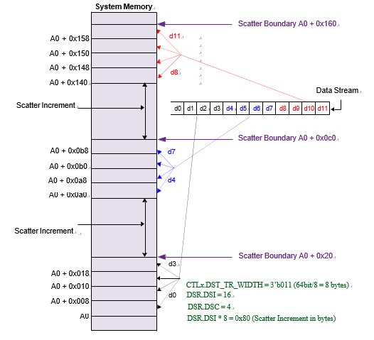
Destination scatter enable bit:0 = Scatter disabled1 =
Scatter enabledScatter on the destination side is applicable
only when the CTLx_L.DINC bit indicates an incrementing
address control and DARx should be aligned with
DST_TR_WIDTH.
Dependencies: This field does not exist if
DMAC_CHx_DST_SCA_EN is not selected.
17
CTL0_L_SRC_GATHER_EN
R/W
0x0
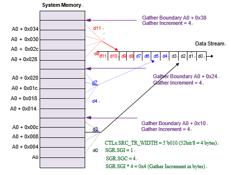
Source gather enable bit:
0 = Gather disabled
1 = Gather enabled
Gather on the source side is applicable only when the
CTLx_L.SINC bit indicates an incrementing address control
and SARx should be aligned with SRC_TR_WIDTH.
Dependencies: This field does not exist if
DMAC_CHx_SRC_GAT_EN is not selected.
16:14
CTL0_L_SRC_MSIZE
R/W
0x1
Source Burst Transaction Length.
Number of data items, each of width CTLx_L.SRC_TR_WIDTH if
source is not memory, otherwise each of width
DMAC_TR_WIDTH_DEFAULT, to be read from the source every time
a source burst transaction request is made from either the
corresponding hardware or software handshaking interface.
Read burst transaction length on bus (ARLen) will not exceed
this value, but may be less than this value. If SINC is
setted to “no change”, this value should not be greater than
16 to conform to the AXI protocol.
If enabled ‘DMAC_CHx_MSIZE_BIGGER_THAN_FIFO_DEPTH’ feature,
to improve performance, can set CTLx_L.SRC_MSIZE to a high
value to make DMAC send longer burst length command. But to
avoid deadlock, if Source slave and Destination slave is the
same slave, should not set CTLx_L.SRC_MSIZE over than
FIFO_depth; Table 6-2-0 lists the decoding for this field.
13:11
CTL0_L_DEST_MSIZE
R/W
0x1
Destination Burst Transaction Length.
Number of data items, each of width DATA_WIDTH, to be
written to the destination every time a destination burst
transaction request is made from either the corresponding
hardware or software handshaking interface.
Write burst transaction length on bus (AWLen) will not
exceed this value, but may be less than this value. If DINC
is setted to “no change”, this value should not be greater
than 16 to conform to the AXI protocol.
If enabled ‘DMAC_CHx_MSIZE_BIGGER_THAN_FIFO_DEPTH’ feature,
to improve performance, can set CTLx_L.SRC_MSIZE to a high
value to make DMAC send longer burst length command. But to
avoid deadlock, if Source slave and Destination slave is the
same slave, should not set CTLx_L.SRC_MSIZE over than
FIFO_depth; Table 6-2-1 lists the decoding for this field.
10:9
CTL0_L_SINC
R/W
0x0
Source Address Increment. Indicates whether to increment the
source address on every source transfer. If the device is
fetching data from a source peripheral FIFO with a fixed
address, then set this field to “No change.”If source is
memory appointed by CTLx_L.TT_FC, and set SINC=No change,
then SRC_TR_WIDTH must be set to BUS width. And DMAC will
read data from the fixed memory address until block transfer
finish, but It is not recommended to read memory like this,
because some memory controller not support fixed burst
transaction and may transform the fixed burst transaction to
incremental burst transaction.
00 = Increment
01 =Not support
1x = No change
备注
Incrementing is done for alignment to the next
CTLx_L.SRC_TR_WIDTH boundary.
8:7
CTL0_L_DINC
R/W
0x0
Destination Address Increment. Indicates whether to
increment destination address on every destination transfer.
If your device is writing data to a destination peripheral
FIFO with a fixed address, then set this field to “No
change.”If destination is memory appointed by CTLx_L.TT_FC,
and set DINC=No change, then DST_TR_WIDTH must be set to BUS
width. And DMAC will write data to the fixed memory address
until block transfer finish, but It is not recommended to
write memory like this, because some memory controller not
support fixed burst transaction and may transform the fixed
burst transaction to incremental burst transaction.
00 = Increment
01=Not Support
1x = No change
备注
Incrementing is done for alignment to the next
CTLx_L.DST_TR_WIDTH boundary.
6:4
CTL0_L_SRC_TR_WIDTH
R/W
0x0
Source Transfer Width.
Table 6-3 lists the decoding for this field.It can’t be
mapped to AXI bus data width directly. Since AXI bus data
width is fixed (such as 32bit/64bit), AXI use byte enable
signal for byte/half word transfer (still burst). So, the
SRC_TR_WIDTH is only used for total block data size
calculation and streaming mode byte/half word transfer (for
FIFO transfer).
备注
SRC_TR_WIDTH must not be bigger than BUS width.
3:1
CTL0_L_DST_TR_WIDTH
R/W
0x0
Destination Transfer Width.Table 6-3 lists the decoding for
this field. It can’t be mapped to AXI bus data width
directly. For a non-memory peripheral, typically the
peripheral (destination) FIFO width.Note: DST_TR_WIDTH must
not be bigger than BUS width
0
CTL0_L_INT_EN
R/W
0x1
Interrupt Enable Bit. If set, then all interrupt-generating
sources are enabled. Functions as a global mask bit for all
interrupts for the channel; raw* interrupt registers still
assert if CTLx_L.INT_EN = 0.
REG_CTL0_H
Name: Channel 0 high-32 bits Control Register
Size: 32
Address offset: 01Ch
Read/write access: R
Control register high for DMA channel x for block size
Bit
Symbol
Access
INI
Description
31:0
CTL0_H_TRANS_DATA_CNT
R
0x0
Data Transfered Count.Once the transfer starts, the
read-back value is the total number of data bytes already
write to destination memory or peripheral.
Configuration register low for DMA channel x, configures transfer parameters
Bit
Symbol
Access
INI
Description
31
CFG0_L_RELOAD_DST
R/W
0x0
Automatic Destination Reload. The DARx register can be
automatically reloaded from its initial value at the end of
every block for multi-block transfers. A new block transfer
is then initiated.This register does not exist if the
configuration parameter DMAC_CHx_MULTI_BLK_EN is not
selected; in this case, the read-back value is always 0.
30
CFG0_L_RELOAD_SRC
R/W
0x0
Automatic Source Reload. The SARx register can be
automatically reloaded from its initial value at the end of
every block for multi-block transfers. A new block transfer
is then initiated.
This field does not exist if the configuration parameter
DMAC_CHx_MULTI_BLK_EN is not selected; in this case, the
read-back value is always 0.
29:20
RSVD
R
-
Reserved
19
CFG0_L_SRC_HS_POL
R/W
0x0
Source Handshaking Interface Polarity.
0 = Active high
1 = Active low
18
CFG0_L_DST_HS_POL
R/W
0x0
Destination Handshaking Interface Polarity.
0 = Active high
1 = Active low
For information on this, refer to “Handshaking Interface” .
17:12
RSVD
R
-
Reserved
11
CFG0_L_HS_SEL_SRC
R/W
0x1
Source Software or Hardware Handshaking Select. This
register selects which of the handshaking interfaces –
hardware or software – is active for source requests on this
channel.
0 = Hardware handshaking interface. Software-initiated
transaction requests are ignored.
1 = Software handshaking interface. Hardware-initiated
transaction requests are ignored. If the source peripheral
is memory, then this bit is ignored.
10
CFG0_L_HS_SEL_DST
R/W
0x1
Destination Software or Hardware Handshaking Select. This
register selects which of the handshaking interfaces –
hardware or software – is active for destination requests on
this channel.
0 = Hardware handshaking interface. Software-initiated
transaction requests are ignored.
1 = Software handshaking interface. Hardware- initiated
transaction requests are ignored. If the destination
peripheral is memory, then this bit is ignored.
9
CFG0_L_FIFO_EMPTY
R
0x1
Indicates if there is data left in the channel FIFO.
1 = Channel FIFO empty
0 = Channel FIFO not empty
8
CFG0_L_CH_SUSP
R/W
0x0
Channel Suspend. Suspends all DMA data transfers from the
source until this bit is cleared. There is no guarantee that
the current transaction will complete. Can also be used in
conjunction with CFGx_l.INACTIVE to cleanly disable a
channel without losing any data.
0 = Not suspended
1 = Suspend DMA transfer from the source.
This field will be reset to 0 after “Disabling a Channel
Prior to Transfer Completion” automatically by hardware.For
more information, refer to “7.7 Disabling a Channel Prior to
Transfer Completion” .
备注
if user not define DMAC_CH*_SUPPORT_SUSPEND, it only
can be readed.
7:4
CFG0_L_CH_PRIOR
R/W
0x0
Channel priority.
RTK DMAC supports three kinds of channel priority now, fixed
priority, round robin priority and programmable priority.
The default way is fixed priority to reduce area, and
channel0 has the highest priority, channel15 has the lowest
priority. Changing the definition of parameter FIX_PRIORITY
or Programmable_PRIORITY can change priority way.
If RTK DMAC is configured to support Programmable priority,
this field will be used to set priority between channels.
CH_PRIOR’s legal value is 0 ~ (DMAC_NUM_CHANNELS-1), and 0
is the highest priority value, (DMAC_NUM_CHANNELS-1) is the
lowest priroty value. If more than one channel are set with
the same priroty value, the channel with small channel
number index has higher priority.
If DMAC is configured to support fix priority or
round-robin priority, this field is not exist.
备注
if user not define ProgrammablePriority, it only can
be readed.
3
RSVD
R
-
Reserved
2
CFG0_L_DST_PCTL_OVER
R
0x1
DMA destination bus protocol finish, indicating the current
write command has finished.
1
CFG0_L_SRC_PCTL_OVER
R
0x1
DMA Source bus protocol finish, indicating the current read
command has finished.
0
CFG0_L_INACTIVE
R
0x1
Indicates if the channel is inactive. Can be used in
conjunction with CFGx_L.CH_SUSP to cleanly disable a channel
when destination is peripheral. For more information, refer
to “Disabling a Channel Prior to Transfer Completion” .
Configuration register high for DMA channel x, configures additional transfer parameters
Bit
Symbol
Access
INI
Description
31:17
RSVD
R
-
Reserved
16
CFG0_H_EXTENDED_DEST_PER1
R/W
0x0
The extened 4th bit of DEST_PER when hardware handshake
interfaces number is configured to 32.
15
CFG0_H_EXTENDED_SRC_PER1
R/W
0x0
The extened 4th bit of SRC_PER when hardware handshake
interfaces number is configured to 32.
14:11
CFG0_H_DEST_PER
R/W
0x0
Assigns a hardware handshaking interface(0 –
DMAC_NUM_HS_INT-1) to the destination of channel x if the
FGx.HS_SEL_DST field is 0; otherwise, this field is ignored.
The channel can then communicate with the
destinationperipheral connected to that interface through
the assignedhardware handshaking interface.
NOTE1: For correct DMA operation, only one peripheral
(sourceor destination) should be assigned to the same
handshaking interface
NOTE2: This field does not exist if the configuration
parameterDMAC_NUM_HS_INT is set to 0.
10:7
CFG0_H_SRC_PER
R/W
0x0
Assigns a hardware handshaking interface(0 –
DMAC_NUM_HS_INT-1) to the source of channel x if the
CFGx.HS_SEL_SRC field is 0; otherwise, this field is
ignored. The channel can then communicate with the source
peripheral connected to that interface through the assigned
hardware handshaking interface.
NOTE1: For correct RTK_DMAC operation, only one peripheral
(source or destination) should be assigned to the same
handshaking interface.
NOTE2: This field does not exist if the configuration
parameter DMAC_NUM_HS_INT is set to 0.
6:4
RSVD
R
-
Reserved
3
CFG0_H_PROTCTL
R/W
0x1
Protection Control.Set the bit 35 to 0 will enable the
channel secure DMA transfer.
Set the bit 35 to 1 will enable the channel non-secure DMAC
transfer.
备注
if user not define DMAC_SECURE_MODE, it only can be
readed.
2:1
RSVD
R
-
Reserved
0
CFG0_H_FCMODE
R/W
0x0
Flow Control Mode. Determines when source transaction
requests are serviced when the Destination Peripheral is the
flow controller.
0 = Source transaction requests are servied when they occur.
Data pre-fetching is enabled.
1 = Source transaction requests are not serviced until a
destination transaction request occurs. Data pre-fetching
is disabled.
备注
Please keep this bit 0 when Transfer Type and Flow
Control is not ”destination peripheral is the flow
controller and transfer type is peripheral to
peripheral” (TT_FC!=7).
REG_SAR1
Name: Channel 1 Source Address Register
Size: 32
Address offset: 058h
Read/write access: R/W
Source address register for DMA channel x, specifies the source memory address
Bit
Symbol
Access
INI
Description
31:0
SAR1
R/W
Unknown
Source Address of DMA transfer.Updated after each source
transfer. The SINC field in the CTLx register determines
whether the address increments, or is left unchanged on
every source transfer throughout the block transfer.
REG_CURR_SAR1
Name: The read back value is channel 1 source reading address at present
Size: 32
Address offset: 05Ch
Read/write access: R
Current source address register for DMA channel x, indicates the current source address during
transfer
Bit
Symbol
Access
INI
Description
31:0
CURR_SAR1
R
0x0
The read back value is source reading address at present
REG_DAR1
Name: Channel 1 Destination Address Register
Size: 32
Address offset: 060h
Read/write access: R/W
Destination address register for DMA channel x, specifies the destination memory address
Bit
Symbol
Access
INI
Description
31:0
DAR1
R/W
Unknown
Destination address of DMA transfer.Updated after each
destination transfer. The DINC field in the CTLx register
determines whether the address increments, or is left
unchanged on every destination transfer throughout the block
transfer.
REG_CURR_DAR1
Name: The read back value is channel 1 destination writing address at present
Size: 32
Address offset: 064h
Read/write access: R
Current destination address register for DMA channel x, indicates the current destination address
during transfer
Bit
Symbol
Access
INI
Description
31:0
CURR_DAR1
R
0x0
The read back value is destination writing address at
present
REG_LLP1_L
Name: Channel 1 low-32 bits Linked List Pointer Register
Size: 32
Address offset: 068h
Read/write access: R/W
Linked list pointer register low for DMA channel x, points to the starting address of linked list
item
Bit
Symbol
Access
INI
Description
31:2
LLP1_L_LOC
R/W
Unknown
Starting Address In Memory of next LLI if block chaining is
enabled. Note that the two LSBs of the starting address are
not stored because the address is assumed to be aligned to a
32-bit boundary.LLI accesses are always 32-bit accesses
aligned to 32-bit boundaries and cannot be changed or
programmed to anything other than 32-bit.
1:0
RSVD
R
-
Reserved
REG_CTL1_L
Name: Channel 1 low-32 bits Control Register
Size: 32
Address offset: 070h
Read/write access: R/W
Control register low for DMA channel x, configures channel control settings
Bit
Symbol
Access
INI
Description
31:29
RSVD
R
-
Reserved
28
CTL1_L_LLP_SRC_EN
R/W
0x0
Block chanining is enabled on the source side only if the
LLP_SRC_EN field id high and LLPx_L.LOC is non-zero; for
more information,see 7.4.1.1 “Block Chaining Using Linked
Lists”
Dependencies:This field does not exist if the configuration
parameterDMAC_CHx_MULTI_BLK_EN is not selected or if
DMAC_CHx_HC_LLP is selected; in this case, the read-back
value is always 0.
27
CTL1_L_LLP_DST_EN
R/W
0x0
Block chanining is enabled on the destination side only if
the LLP_DST_EN field id high and LLPx_L.LOC is non-zero;
for more information,see 7.4.1.1 “Block Chaining Using
Linked Lists”
Dependencies:This field does not exist if the configuration
parameterDMAC_CHx_MULTI_BLK_EN is not selected or if
DMAC_CHx_HC_LLP is selected; in this case, the read-back
value is always 0.
26:23
RSVD
R
-
Reserved
22:20
CTL1_L_TT_FC
R/W
0x0
Transfer Type and Flow Control.The following transfer types
are supported.
Memory to Memory
Memory to Peripheral
Peripheral to Memory
Peripheral to Peripheral
Flow Control can be assigned to the RTK_DMAC, the source
peripheral, or the destination peripheral. Table 6-4 lists
the decoding for this field. For more information on
transfer types and flow control, refer to “Setup/Operation
of RTK_DMAC Transfers”.
Reset Value: 3’h0
Dependencies: If hardware handshake isn’t support, then
TT_FC can only be set to 3’b0. TT_FC[2] can only be read.
19
RSVD
R
-
Reserved
18
CTL1_L_DST_SCATTER_EN
R/W
0x0
Destination scatter enable bit:0 = Scatter disabled1 =
Scatter enabledScatter on the destination side is applicable
only when the CTLx_L.DINC bit indicates an incrementing
address control and DARx should be aligned with
DST_TR_WIDTH.
Dependencies: This field does not exist if
DMAC_CHx_DST_SCA_EN is not selected.
17
CTL1_L_SRC_GATHER_EN
R/W
0x0
Source gather enable bit:
0 = Gather disabled
1 = Gather enabled
Gather on the source side is applicable only when the
CTLx_L.SINC bit indicates an incrementing address control
and SARx should be aligned with SRC_TR_WIDTH.
Dependencies: This field does not exist if
DMAC_CHx_SRC_GAT_EN is not selected.
16:14
CTL1_L_SRC_MSIZE
R/W
0x1
Source Burst Transaction Length.
Number of data items, each of width CTLx_L.SRC_TR_WIDTH if
source is not memory, otherwise each of width
DMAC_TR_WIDTH_DEFAULT, to be read from the source every time
a source burst transaction request is made from either the
corresponding hardware or software handshaking interface.
Read burst transaction length on bus (ARLen) will not exceed
this value, but may be less than this value. If SINC is
setted to “no change”, this value should not be greater than
16 to conform to the AXI protocol.
If enabled ‘DMAC_CHx_MSIZE_BIGGER_THAN_FIFO_DEPTH’ feature,
to improve performance, can set CTLx_L.SRC_MSIZE to a high
value to make DMAC send longer burst length command. But to
avoid deadlock, if Source slave and Destination slave is the
same slave, should not set CTLx_L.SRC_MSIZE over than
FIFO_depth; Table 6-2-0 lists the decoding for this field.
13:11
CTL1_L_DEST_MSIZE
R/W
0x1
Destination Burst Transaction Length.
Number of data items, each of width DATA_WIDTH, to be
written to the destination every time a destination burst
transaction request is made from either the corresponding
hardware or software handshaking interface.
Write burst transaction length on bus (AWLen) will not
exceed this value, but may be less than this value. If DINC
is setted to “no change”, this value should not be greater
than 16 to conform to the AXI protocol.
If enabled ‘DMAC_CHx_MSIZE_BIGGER_THAN_FIFO_DEPTH’ feature,
to improve performance, can set CTLx_L.SRC_MSIZE to a high
value to make DMAC send longer burst length command. But to
avoid deadlock, if Source slave and Destination slave is the
same slave, should not set CTLx_L.SRC_MSIZE over than
FIFO_depth; Table 6-2-1 lists the decoding for this field.
10:9
CTL1_L_SINC
R/W
0x0
Source Address Increment. Indicates whether to increment the
source address on every source transfer. If the device is
fetching data from a source peripheral FIFO with a fixed
address, then set this field to “No change.”If source is
memory appointed by CTLx_L.TT_FC, and set SINC=No change,
then SRC_TR_WIDTH must be set to BUS width. And DMAC will
read data from the fixed memory address until block transfer
finish, but It is not recommended to read memory like this,
because some memory controller not support fixed burst
transaction and may transform the fixed burst transaction to
incremental burst transaction.
00 = Increment
01 =Not support
1x = No change
备注
Incrementing is done for alignment to the next
CTLx_L.SRC_TR_WIDTH boundary.
8:7
CTL1_L_DINC
R/W
0x0
Destination Address Increment. Indicates whether to
increment destination address on every destination transfer.
If your device is writing data to a destination peripheral
FIFO with a fixed address, then set this field to “No
change.”If destination is memory appointed by CTLx_L.TT_FC,
and set DINC=No change, then DST_TR_WIDTH must be set to BUS
width. And DMAC will write data to the fixed memory address
until block transfer finish, but It is not recommended to
write memory like this, because some memory controller not
support fixed burst transaction and may transform the fixed
burst transaction to incremental burst transaction.
00 = Increment
01=Not Support
1x = No change
备注
Incrementing is done for alignment to the next
CTLx_L.DST_TR_WIDTH boundary.
6:4
CTL1_L_SRC_TR_WIDTH
R/W
0x0
Source Transfer Width.
Table 6-3 lists the decoding for this field.It can’t be
mapped to AXI bus data width directly. Since AXI bus data
width is fixed (such as 32bit/64bit), AXI use byte enable
signal for byte/half word transfer (still burst). So, the
SRC_TR_WIDTH is only used for total block data size
calculation and streaming mode byte/half word transfer (for
FIFO transfer).
备注
SRC_TR_WIDTH must not be bigger than BUS width.
3:1
CTL1_L_DST_TR_WIDTH
R/W
0x0
Destination Transfer Width.Table 6-3 lists the decoding for
this field. It can’t be mapped to AXI bus data width
directly. For a non-memory peripheral, typically the
peripheral (destination) FIFO width.Note: DST_TR_WIDTH must
not be bigger than BUS width
0
CTL1_L_INT_EN
R/W
0x1
Interrupt Enable Bit. If set, then all interrupt-generating
sources are enabled. Functions as a global mask bit for all
interrupts for the channel; raw* interrupt registers still
assert if CTLx_L.INT_EN = 0.
REG_CTL1_H
Name: Channel 1 high-32 bits Control Register
Size: 32
Address offset: 074h
Read/write access: R
Control register high for DMA channel x for block size
Bit
Symbol
Access
INI
Description
31:0
CTL1_H_TRANS_DATA_CNT
R
0x0
Data Transfered Count.Once the transfer starts, the
read-back value is the total number of data bytes already
write to destination memory or peripheral.
Configuration register low for DMA channel x, configures transfer parameters
Bit
Symbol
Access
INI
Description
31
CFG1_L_RELOAD_DST
R/W
0x0
Automatic Destination Reload. The DARx register can be
automatically reloaded from its initial value at the end of
every block for multi-block transfers. A new block transfer
is then initiated.This register does not exist if the
configuration parameter DMAC_CHx_MULTI_BLK_EN is not
selected; in this case, the read-back value is always 0.
30
CFG1_L_RELOAD_SRC
R/W
0x0
Automatic Source Reload. The SARx register can be
automatically reloaded from its initial value at the end of
every block for multi-block transfers. A new block transfer
is then initiated.
This field does not exist if the configuration parameter
DMAC_CHx_MULTI_BLK_EN is not selected; in this case, the
read-back value is always 0.
29:20
RSVD
R
-
Reserved
19
CFG1_L_SRC_HS_POL
R/W
0x0
Source Handshaking Interface Polarity.
0 = Active high
1 = Active low
18
CFG1_L_DST_HS_POL
R/W
0x0
Destination Handshaking Interface Polarity.
0 = Active high
1 = Active low
For information on this, refer to “Handshaking Interface” .
17:12
RSVD
R
-
Reserved
11
CFG1_L_HS_SEL_SRC
R/W
0x1
Source Software or Hardware Handshaking Select. This
register selects which of the handshaking interfaces –
hardware or software – is active for source requests on this
channel.
0 = Hardware handshaking interface. Software-initiated
transaction requests are ignored.
1 = Software handshaking interface. Hardware-initiated
transaction requests are ignored. If the source peripheral
is memory, then this bit is ignored.
10
CFG1_L_HS_SEL_DST
R/W
0x1
Destination Software or Hardware Handshaking Select. This
register selects which of the handshaking interfaces –
hardware or software – is active for destination requests on
this channel.
0 = Hardware handshaking interface. Software-initiated
transaction requests are ignored.
1 = Software handshaking interface. Hardware- initiated
transaction requests are ignored. If the destination
peripheral is memory, then this bit is ignored.
9
CFG1_L_FIFO_EMPTY
R
0x1
Indicates if there is data left in the channel FIFO.
1 = Channel FIFO empty
0 = Channel FIFO not empty
8
CFG1_L_CH_SUSP
R/W
0x0
Channel Suspend. Suspends all DMA data transfers from the
source until this bit is cleared. There is no guarantee that
the current transaction will complete. Can also be used in
conjunction with CFGx_l.INACTIVE to cleanly disable a
channel without losing any data.
0 = Not suspended
1 = Suspend DMA transfer from the source.
This field will be reset to 0 after “Disabling a Channel
Prior to Transfer Completion” automatically by hardware.For
more information, refer to “7.7 Disabling a Channel Prior to
Transfer Completion” .
备注
if user not define DMAC_CH*_SUPPORT_SUSPEND, it only
can be readed.
7:4
CFG1_L_CH_PRIOR
R/W
0x0
Channel priority.
RTK DMAC supports three kinds of channel priority now, fixed
priority, round robin priority and programmable priority.
The default way is fixed priority to reduce area, and
channel0 has the highest priority, channel15 has the lowest
priority. Changing the definition of parameter FIX_PRIORITY
or Programmable_PRIORITY can change priority way.
If RTK DMAC is configured to support Programmable priority,
this field will be used to set priority between channels.
CH_PRIOR’s legal value is 0 ~ (DMAC_NUM_CHANNELS-1), and 0
is the highest priority value, (DMAC_NUM_CHANNELS-1) is the
lowest priroty value. If more than one channel are set with
the same priroty value, the channel with small channel
number index has higher priority.
If DMAC is configured to support fix priority or
round-robin priority, this field is not exist.
备注
if user not define ProgrammablePriority, it only can
be readed.
3
RSVD
R
-
Reserved
2
CFG1_L_DST_PCTL_OVER
R
0x1
DMA destination bus protocol finish, indicating the current
write command has finished.
1
CFG1_L_SRC_PCTL_OVER
R
0x1
DMA Source bus protocol finish, indicating the current read
command has finished.
0
CFG1_L_INACTIVE
R
0x1
Indicates if the channel is inactive. Can be used in
conjunction with CFGx_L.CH_SUSP to cleanly disable a channel
when destination is peripheral. For more information, refer
to “Disabling a Channel Prior to Transfer Completion” .
Configuration register high for DMA channel x, configures additional transfer parameters
Bit
Symbol
Access
INI
Description
31:17
RSVD
R
-
Reserved
16
CFG1_H_EXTENDED_DEST_PER1
R/W
0x0
The extened 4th bit of DEST_PER when hardware handshake
interfaces number is configured to 32.
15
CFG1_H_EXTENDED_SRC_PER1
R/W
0x0
The extened 4th bit of SRC_PER when hardware handshake
interfaces number is configured to 32.
14:11
CFG1_H_DEST_PER
R/W
0x0
Assigns a hardware handshaking interface(0 –
DMAC_NUM_HS_INT-1) to the destination of channel x if the
FGx.HS_SEL_DST field is 0; otherwise, this field is ignored.
The channel can then communicate with the
destinationperipheral connected to that interface through
the assignedhardware handshaking interface.
NOTE1: For correct DMA operation, only one peripheral
(sourceor destination) should be assigned to the same
handshaking interface
NOTE2: This field does not exist if the configuration
parameterDMAC_NUM_HS_INT is set to 0.
10:7
CFG1_H_SRC_PER
R/W
0x0
Assigns a hardware handshaking interface(0 –
DMAC_NUM_HS_INT-1) to the source of channel x if the
CFGx.HS_SEL_SRC field is 0; otherwise, this field is
ignored. The channel can then communicate with the source
peripheral connected to that interface through the assigned
hardware handshaking interface.
NOTE1: For correct RTK_DMAC operation, only one peripheral
(source or destination) should be assigned to the same
handshaking interface.
NOTE2: This field does not exist if the configuration
parameter DMAC_NUM_HS_INT is set to 0.
6:4
RSVD
R
-
Reserved
3
CFG1_H_PROTCTL
R/W
0x1
Protection Control.Set the bit 35 to 0 will enable the
channel secure DMA transfer.
Set the bit 35 to 1 will enable the channel non-secure DMAC
transfer.
备注
if user not define DMAC_SECURE_MODE, it only can be
readed.
2:1
RSVD
R
-
Reserved
0
CFG1_H_FCMODE
R/W
0x0
Flow Control Mode. Determines when source transaction
requests are serviced when the Destination Peripheral is the
flow controller.
0 = Source transaction requests are servied when they occur.
Data pre-fetching is enabled.
1 = Source transaction requests are not serviced until a
destination transaction request occurs. Data pre-fetching
is disabled.
备注
Please keep this bit 0 when Transfer Type and Flow
Control is not ”destination peripheral is the flow
controller and transfer type is peripheral to
peripheral” (TT_FC!=7).
REG_SAR2
Name: Channel 2 Source Address Register
Size: 32
Address offset: 0B0h
Read/write access: R/W
Source address register for DMA channel x, specifies the source memory address
Bit
Symbol
Access
INI
Description
31:0
SAR2
R/W
Unknown
Source Address of DMA transfer.Updated after each source
transfer. The SINC field in the CTLx register determines
whether the address increments, or is left unchanged on
every source transfer throughout the block transfer.
REG_CURR_SAR2
Name: The read back value is channel 2 source reading address at present
Size: 32
Address offset: 0B4h
Read/write access: R
Current source address register for DMA channel x, indicates the current source address during
transfer
Bit
Symbol
Access
INI
Description
31:0
CURR_SAR2
R
0x0
The read back value is source reading address at present
REG_DAR2
Name: Channel 2 Destination Address Register
Size: 32
Address offset: 0B8h
Read/write access: R/W
Destination address register for DMA channel x, specifies the destination memory address
Bit
Symbol
Access
INI
Description
31:0
DAR2
R/W
Unknown
Destination address of DMA transfer.Updated after each
destination transfer. The DINC field in the CTLx register
determines whether the address increments, or is left
unchanged on every destination transfer throughout the block
transfer.
REG_CURR_DAR2
Name: The read back value is channel 2 destination writing address at present
Size: 32
Address offset: 0BCh
Read/write access: R
Current destination address register for DMA channel x, indicates the current destination address
during transfer
Bit
Symbol
Access
INI
Description
31:0
CURR_DAR2
R
0x0
The read back value is destination writing address at
present
REG_LLP2_L
Name: Channel 2 low-32 bits Linked List Pointer Register
Size: 32
Address offset: 0C0h
Read/write access: R/W
Linked list pointer register low for DMA channel x, points to the starting address of linked list
item
Bit
Symbol
Access
INI
Description
31:2
LLP2_L_LOC
R/W
Unknown
Starting Address In Memory of next LLI if block chaining is
enabled. Note that the two LSBs of the starting address are
not stored because the address is assumed to be aligned to a
32-bit boundary.LLI accesses are always 32-bit accesses
aligned to 32-bit boundaries and cannot be changed or
programmed to anything other than 32-bit.
1:0
RSVD
R
-
Reserved
REG_CTL2_L
Name: Channel 2 low-32 bits Control Register
Size: 32
Address offset: 0C8h
Read/write access: R/W
Control register low for DMA channel x, configures channel control settings
Bit
Symbol
Access
INI
Description
31:29
RSVD
R
-
Reserved
28
CTL2_L_LLP_SRC_EN
R/W
0x0
Block chanining is enabled on the source side only if the
LLP_SRC_EN field id high and LLPx_L.LOC is non-zero; for
more information,see 7.4.1.1 “Block Chaining Using Linked
Lists”
Dependencies:This field does not exist if the configuration
parameterDMAC_CHx_MULTI_BLK_EN is not selected or if
DMAC_CHx_HC_LLP is selected; in this case, the read-back
value is always 0.
27
CTL2_L_LLP_DST_EN
R/W
0x0
Block chanining is enabled on the destination side only if
the LLP_DST_EN field id high and LLPx_L.LOC is non-zero;
for more information,see 7.4.1.1 “Block Chaining Using
Linked Lists”
Dependencies:This field does not exist if the configuration
parameterDMAC_CHx_MULTI_BLK_EN is not selected or if
DMAC_CHx_HC_LLP is selected; in this case, the read-back
value is always 0.
26:23
RSVD
R
-
Reserved
22:20
CTL2_L_TT_FC
R/W
0x0
Transfer Type and Flow Control.The following transfer types
are supported.
Memory to Memory
Memory to Peripheral
Peripheral to Memory
Peripheral to Peripheral
Flow Control can be assigned to the RTK_DMAC, the source
peripheral, or the destination peripheral. Table 6-4 lists
the decoding for this field. For more information on
transfer types and flow control, refer to “Setup/Operation
of RTK_DMAC Transfers”.
Reset Value: 3’h0
Dependencies: If hardware handshake isn’t support, then
TT_FC can only be set to 3’b0. TT_FC[2] can only be read.
19
RSVD
R
-
Reserved
18
CTL2_L_DST_SCATTER_EN
R/W
0x0
Destination scatter enable bit:0 = Scatter disabled1 =
Scatter enabledScatter on the destination side is applicable
only when the CTLx_L.DINC bit indicates an incrementing
address control and DARx should be aligned with
DST_TR_WIDTH.
Dependencies: This field does not exist if
DMAC_CHx_DST_SCA_EN is not selected.
17
CTL2_L_SRC_GATHER_EN
R/W
0x0
Source gather enable bit:
0 = Gather disabled
1 = Gather enabled
Gather on the source side is applicable only when the
CTLx_L.SINC bit indicates an incrementing address control
and SARx should be aligned with SRC_TR_WIDTH.
Dependencies: This field does not exist if
DMAC_CHx_SRC_GAT_EN is not selected.
16:14
CTL2_L_SRC_MSIZE
R/W
0x1
Source Burst Transaction Length.
Number of data items, each of width CTLx_L.SRC_TR_WIDTH if
source is not memory, otherwise each of width
DMAC_TR_WIDTH_DEFAULT, to be read from the source every time
a source burst transaction request is made from either the
corresponding hardware or software handshaking interface.
Read burst transaction length on bus (ARLen) will not exceed
this value, but may be less than this value. If SINC is
setted to “no change”, this value should not be greater than
16 to conform to the AXI protocol.
If enabled ‘DMAC_CHx_MSIZE_BIGGER_THAN_FIFO_DEPTH’ feature,
to improve performance, can set CTLx_L.SRC_MSIZE to a high
value to make DMAC send longer burst length command. But to
avoid deadlock, if Source slave and Destination slave is the
same slave, should not set CTLx_L.SRC_MSIZE over than
FIFO_depth; Table 6-2-0 lists the decoding for this field.
13:11
CTL2_L_DEST_MSIZE
R/W
0x1
Destination Burst Transaction Length.
Number of data items, each of width DATA_WIDTH, to be
written to the destination every time a destination burst
transaction request is made from either the corresponding
hardware or software handshaking interface.
Write burst transaction length on bus (AWLen) will not
exceed this value, but may be less than this value. If DINC
is setted to “no change”, this value should not be greater
than 16 to conform to the AXI protocol.
If enabled ‘DMAC_CHx_MSIZE_BIGGER_THAN_FIFO_DEPTH’ feature,
to improve performance, can set CTLx_L.SRC_MSIZE to a high
value to make DMAC send longer burst length command. But to
avoid deadlock, if Source slave and Destination slave is the
same slave, should not set CTLx_L.SRC_MSIZE over than
FIFO_depth; Table 6-2-1 lists the decoding for this field.
10:9
CTL2_L_SINC
R/W
0x0
Source Address Increment. Indicates whether to increment the
source address on every source transfer. If the device is
fetching data from a source peripheral FIFO with a fixed
address, then set this field to “No change.”If source is
memory appointed by CTLx_L.TT_FC, and set SINC=No change,
then SRC_TR_WIDTH must be set to BUS width. And DMAC will
read data from the fixed memory address until block transfer
finish, but It is not recommended to read memory like this,
because some memory controller not support fixed burst
transaction and may transform the fixed burst transaction to
incremental burst transaction.
00 = Increment
01 =Not support
1x = No change
备注
Incrementing is done for alignment to the next
CTLx_L.SRC_TR_WIDTH boundary.
8:7
CTL2_L_DINC
R/W
0x0
Destination Address Increment. Indicates whether to
increment destination address on every destination transfer.
If your device is writing data to a destination peripheral
FIFO with a fixed address, then set this field to “No
change.”If destination is memory appointed by CTLx_L.TT_FC,
and set DINC=No change, then DST_TR_WIDTH must be set to BUS
width. And DMAC will write data to the fixed memory address
until block transfer finish, but It is not recommended to
write memory like this, because some memory controller not
support fixed burst transaction and may transform the fixed
burst transaction to incremental burst transaction.
00 = Increment
01=Not Support
1x = No change
备注
Incrementing is done for alignment to the next
CTLx_L.DST_TR_WIDTH boundary.
6:4
CTL2_L_SRC_TR_WIDTH
R/W
0x0
Source Transfer Width.
Table 6-3 lists the decoding for this field.It can’t be
mapped to AXI bus data width directly. Since AXI bus data
width is fixed (such as 32bit/64bit), AXI use byte enable
signal for byte/half word transfer (still burst). So, the
SRC_TR_WIDTH is only used for total block data size
calculation and streaming mode byte/half word transfer (for
FIFO transfer).
备注
SRC_TR_WIDTH must not be bigger than BUS width.
3:1
CTL2_L_DST_TR_WIDTH
R/W
0x0
Destination Transfer Width.Table 6-3 lists the decoding for
this field. It can’t be mapped to AXI bus data width
directly. For a non-memory peripheral, typically the
peripheral (destination) FIFO width.Note: DST_TR_WIDTH must
not be bigger than BUS width
0
CTL2_L_INT_EN
R/W
0x1
Interrupt Enable Bit. If set, then all interrupt-generating
sources are enabled. Functions as a global mask bit for all
interrupts for the channel; raw* interrupt registers still
assert if CTLx_L.INT_EN = 0.
REG_CTL2_H
Name: Channel 2 high-32 bits Control Register
Size: 32
Address offset: 0CCh
Read/write access: R
Control register high for DMA channel x for block size
Bit
Symbol
Access
INI
Description
31:0
CTL2_H_TRANS_DATA_CNT
R
0x0
Data Transfered Count.Once the transfer starts, the
read-back value is the total number of data bytes already
write to destination memory or peripheral.
Configuration register low for DMA channel x, configures transfer parameters
Bit
Symbol
Access
INI
Description
31
CFG2_L_RELOAD_DST
R/W
0x0
Automatic Destination Reload. The DARx register can be
automatically reloaded from its initial value at the end of
every block for multi-block transfers. A new block transfer
is then initiated.This register does not exist if the
configuration parameter DMAC_CHx_MULTI_BLK_EN is not
selected; in this case, the read-back value is always 0.
30
CFG2_L_RELOAD_SRC
R/W
0x0
Automatic Source Reload. The SARx register can be
automatically reloaded from its initial value at the end of
every block for multi-block transfers. A new block transfer
is then initiated.
This field does not exist if the configuration parameter
DMAC_CHx_MULTI_BLK_EN is not selected; in this case, the
read-back value is always 0.
29:20
RSVD
R
-
Reserved
19
CFG2_L_SRC_HS_POL
R/W
0x0
Source Handshaking Interface Polarity.
0 = Active high
1 = Active low
18
CFG2_L_DST_HS_POL
R/W
0x0
Destination Handshaking Interface Polarity.
0 = Active high
1 = Active low
For information on this, refer to “Handshaking Interface” .
17:12
RSVD
R
-
Reserved
11
CFG2_L_HS_SEL_SRC
R/W
0x1
Source Software or Hardware Handshaking Select. This
register selects which of the handshaking interfaces –
hardware or software – is active for source requests on this
channel.
0 = Hardware handshaking interface. Software-initiated
transaction requests are ignored.
1 = Software handshaking interface. Hardware-initiated
transaction requests are ignored. If the source peripheral
is memory, then this bit is ignored.
10
CFG2_L_HS_SEL_DST
R/W
0x1
Destination Software or Hardware Handshaking Select. This
register selects which of the handshaking interfaces –
hardware or software – is active for destination requests on
this channel.
0 = Hardware handshaking interface. Software-initiated
transaction requests are ignored.
1 = Software handshaking interface. Hardware- initiated
transaction requests are ignored. If the destination
peripheral is memory, then this bit is ignored.
9
CFG2_L_FIFO_EMPTY
R
0x1
Indicates if there is data left in the channel FIFO.
1 = Channel FIFO empty
0 = Channel FIFO not empty
8
CFG2_L_CH_SUSP
R/W
0x0
Channel Suspend. Suspends all DMA data transfers from the
source until this bit is cleared. There is no guarantee that
the current transaction will complete. Can also be used in
conjunction with CFGx_l.INACTIVE to cleanly disable a
channel without losing any data.
0 = Not suspended
1 = Suspend DMA transfer from the source.
This field will be reset to 0 after “Disabling a Channel
Prior to Transfer Completion” automatically by hardware.For
more information, refer to “7.7 Disabling a Channel Prior to
Transfer Completion” .
备注
if user not define DMAC_CH*_SUPPORT_SUSPEND, it only
can be readed.
7:4
CFG2_L_CH_PRIOR
R/W
0x0
Channel priority.
RTK DMAC supports three kinds of channel priority now, fixed
priority, round robin priority and programmable priority.
The default way is fixed priority to reduce area, and
channel0 has the highest priority, channel15 has the lowest
priority. Changing the definition of parameter FIX_PRIORITY
or Programmable_PRIORITY can change priority way.
If RTK DMAC is configured to support Programmable priority,
this field will be used to set priority between channels.
CH_PRIOR’s legal value is 0 ~ (DMAC_NUM_CHANNELS-1), and 0
is the highest priority value, (DMAC_NUM_CHANNELS-1) is the
lowest priroty value. If more than one channel are set with
the same priroty value, the channel with small channel
number index has higher priority.
If DMAC is configured to support fix priority or
round-robin priority, this field is not exist.
备注
if user not define ProgrammablePriority, it only can
be readed.
3
RSVD
R
-
Reserved
2
CFG2_L_DST_PCTL_OVER
R
0x1
DMA destination bus protocol finish, indicating the current
write command has finished.
1
CFG2_L_SRC_PCTL_OVER
R
0x1
DMA Source bus protocol finish, indicating the current read
command has finished.
0
CFG2_L_INACTIVE
R
0x1
Indicates if the channel is inactive. Can be used in
conjunction with CFGx_L.CH_SUSP to cleanly disable a channel
when destination is peripheral. For more information, refer
to “Disabling a Channel Prior to Transfer Completion” .
Configuration register high for DMA channel x, configures additional transfer parameters
Bit
Symbol
Access
INI
Description
31:17
RSVD
R
-
Reserved
16
CFG2_H_EXTENDED_DEST_PER1
R/W
0x0
The extened 4th bit of DEST_PER when hardware handshake
interfaces number is configured to 32.
15
CFG2_H_EXTENDED_SRC_PER1
R/W
0x0
The extened 4th bit of SRC_PER when hardware handshake
interfaces number is configured to 32.
14:11
CFG2_H_DEST_PER
R/W
0x0
Assigns a hardware handshaking interface(0 –
DMAC_NUM_HS_INT-1) to the destination of channel x if the
FGx.HS_SEL_DST field is 0; otherwise, this field is ignored.
The channel can then communicate with the
destinationperipheral connected to that interface through
the assignedhardware handshaking interface.
NOTE1: For correct DMA operation, only one peripheral
(sourceor destination) should be assigned to the same
handshaking interface
NOTE2: This field does not exist if the configuration
parameterDMAC_NUM_HS_INT is set to 0.
10:7
CFG2_H_SRC_PER
R/W
0x0
Assigns a hardware handshaking interface(0 –
DMAC_NUM_HS_INT-1) to the source of channel x if the
CFGx.HS_SEL_SRC field is 0; otherwise, this field is
ignored. The channel can then communicate with the source
peripheral connected to that interface through the assigned
hardware handshaking interface.
NOTE1: For correct RTK_DMAC operation, only one peripheral
(source or destination) should be assigned to the same
handshaking interface.
NOTE2: This field does not exist if the configuration
parameter DMAC_NUM_HS_INT is set to 0.
6:4
RSVD
R
-
Reserved
3
CFG2_H_PROTCTL
R/W
0x1
Protection Control.Set the bit 35 to 0 will enable the
channel secure DMA transfer.
Set the bit 35 to 1 will enable the channel non-secure DMAC
transfer.
备注
if user not define DMAC_SECURE_MODE, it only can be
readed.
2:1
RSVD
R
-
Reserved
0
CFG2_H_FCMODE
R/W
0x0
Flow Control Mode. Determines when source transaction
requests are serviced when the Destination Peripheral is the
flow controller.
0 = Source transaction requests are servied when they occur.
Data pre-fetching is enabled.
1 = Source transaction requests are not serviced until a
destination transaction request occurs. Data pre-fetching
is disabled.
备注
Please keep this bit 0 when Transfer Type and Flow
Control is not ”destination peripheral is the flow
controller and transfer type is peripheral to
peripheral” (TT_FC!=7).
REG_SAR3
Name: Channel 3 Source Address Register
Size: 32
Address offset: 108h
Read/write access: R/W
Source address register for DMA channel x, specifies the source memory address
Bit
Symbol
Access
INI
Description
31:0
SAR3
R/W
Unknown
Source Address of DMA transfer.Updated after each source
transfer. The SINC field in the CTLx register determines
whether the address increments, or is left unchanged on
every source transfer throughout the block transfer.
REG_CURR_SAR3
Name: The read back value is channel 3 source reading address at present
Size: 32
Address offset: 10Ch
Read/write access: R
Current source address register for DMA channel x, indicates the current source address during
transfer
Bit
Symbol
Access
INI
Description
31:0
CURR_SAR3
R
0x0
The read back value is source reading address at present
REG_DAR3
Name: Channel 3 Destination Address Register
Size: 32
Address offset: 110h
Read/write access: R/W
Destination address register for DMA channel x, specifies the destination memory address
Bit
Symbol
Access
INI
Description
31:0
DAR3
R/W
Unknown
Destination address of DMA transfer.Updated after each
destination transfer. The DINC field in the CTLx register
determines whether the address increments, or is left
unchanged on every destination transfer throughout the block
transfer.
REG_CURR_DAR3
Name: The read back value is channel 3 destination writing address at present
Size: 32
Address offset: 114h
Read/write access: R
Current destination address register for DMA channel x, indicates the current destination address
during transfer
Bit
Symbol
Access
INI
Description
31:0
CURR_DAR3
R
0x0
The read back value is destination writing address at
present
REG_LLP3_L
Name: Channel 3 low-32 bits Linked List Pointer Register
Size: 32
Address offset: 118h
Read/write access: R/W
Linked list pointer register low for DMA channel x, points to the starting address of linked list
item
Bit
Symbol
Access
INI
Description
31:2
LLP3_L_LOC
R/W
Unknown
Starting Address In Memory of next LLI if block chaining is
enabled. Note that the two LSBs of the starting address are
not stored because the address is assumed to be aligned to a
32-bit boundary.LLI accesses are always 32-bit accesses
aligned to 32-bit boundaries and cannot be changed or
programmed to anything other than 32-bit.
1:0
RSVD
R
-
Reserved
REG_CTL3_L
Name: Channel 3 low-32 bits Control Register
Size: 32
Address offset: 120h
Read/write access: R/W
Control register low for DMA channel x, configures channel control settings
Bit
Symbol
Access
INI
Description
31:29
RSVD
R
-
Reserved
28
CTL3_L_LLP_SRC_EN
R/W
0x0
Block chanining is enabled on the source side only if the
LLP_SRC_EN field id high and LLPx_L.LOC is non-zero; for
more information,see 7.4.1.1 “Block Chaining Using Linked
Lists”
Dependencies:This field does not exist if the configuration
parameterDMAC_CHx_MULTI_BLK_EN is not selected or if
DMAC_CHx_HC_LLP is selected; in this case, the read-back
value is always 0.
27
CTL3_L_LLP_DST_EN
R/W
0x0
Block chanining is enabled on the destination side only if
the LLP_DST_EN field id high and LLPx_L.LOC is non-zero;
for more information,see 7.4.1.1 “Block Chaining Using
Linked Lists”
Dependencies:This field does not exist if the configuration
parameterDMAC_CHx_MULTI_BLK_EN is not selected or if
DMAC_CHx_HC_LLP is selected; in this case, the read-back
value is always 0.
26:23
RSVD
R
-
Reserved
22:20
CTL3_L_TT_FC
R/W
0x0
Transfer Type and Flow Control.The following transfer types
are supported.
Memory to Memory
Memory to Peripheral
Peripheral to Memory
Peripheral to Peripheral
Flow Control can be assigned to the RTK_DMAC, the source
peripheral, or the destination peripheral. Table 6-4 lists
the decoding for this field. For more information on
transfer types and flow control, refer to “Setup/Operation
of RTK_DMAC Transfers”.
Reset Value: 3’h0
Dependencies: If hardware handshake isn’t support, then
TT_FC can only be set to 3’b0. TT_FC[2] can only be read.
19
RSVD
R
-
Reserved
18
CTL3_L_DST_SCATTER_EN
R/W
0x0
Destination scatter enable bit:0 = Scatter disabled1 =
Scatter enabledScatter on the destination side is applicable
only when the CTLx_L.DINC bit indicates an incrementing
address control and DARx should be aligned with
DST_TR_WIDTH.
Dependencies: This field does not exist if
DMAC_CHx_DST_SCA_EN is not selected.
17
CTL3_L_SRC_GATHER_EN
R/W
0x0
Source gather enable bit:
0 = Gather disabled
1 = Gather enabled
Gather on the source side is applicable only when the
CTLx_L.SINC bit indicates an incrementing address control
and SARx should be aligned with SRC_TR_WIDTH.
Dependencies: This field does not exist if
DMAC_CHx_SRC_GAT_EN is not selected.
16:14
CTL3_L_SRC_MSIZE
R/W
0x1
Source Burst Transaction Length.
Number of data items, each of width CTLx_L.SRC_TR_WIDTH if
source is not memory, otherwise each of width
DMAC_TR_WIDTH_DEFAULT, to be read from the source every time
a source burst transaction request is made from either the
corresponding hardware or software handshaking interface.
Read burst transaction length on bus (ARLen) will not exceed
this value, but may be less than this value. If SINC is
setted to “no change”, this value should not be greater than
16 to conform to the AXI protocol.
If enabled ‘DMAC_CHx_MSIZE_BIGGER_THAN_FIFO_DEPTH’ feature,
to improve performance, can set CTLx_L.SRC_MSIZE to a high
value to make DMAC send longer burst length command. But to
avoid deadlock, if Source slave and Destination slave is the
same slave, should not set CTLx_L.SRC_MSIZE over than
FIFO_depth; Table 6-2-0 lists the decoding for this field.
13:11
CTL3_L_DEST_MSIZE
R/W
0x1
Destination Burst Transaction Length.
Number of data items, each of width DATA_WIDTH, to be
written to the destination every time a destination burst
transaction request is made from either the corresponding
hardware or software handshaking interface.
Write burst transaction length on bus (AWLen) will not
exceed this value, but may be less than this value. If DINC
is setted to “no change”, this value should not be greater
than 16 to conform to the AXI protocol.
If enabled ‘DMAC_CHx_MSIZE_BIGGER_THAN_FIFO_DEPTH’ feature,
to improve performance, can set CTLx_L.SRC_MSIZE to a high
value to make DMAC send longer burst length command. But to
avoid deadlock, if Source slave and Destination slave is the
same slave, should not set CTLx_L.SRC_MSIZE over than
FIFO_depth; Table 6-2-1 lists the decoding for this field.
10:9
CTL3_L_SINC
R/W
0x0
Source Address Increment. Indicates whether to increment the
source address on every source transfer. If the device is
fetching data from a source peripheral FIFO with a fixed
address, then set this field to “No change.”If source is
memory appointed by CTLx_L.TT_FC, and set SINC=No change,
then SRC_TR_WIDTH must be set to BUS width. And DMAC will
read data from the fixed memory address until block transfer
finish, but It is not recommended to read memory like this,
because some memory controller not support fixed burst
transaction and may transform the fixed burst transaction to
incremental burst transaction.
00 = Increment
01 =Not support
1x = No change
备注
Incrementing is done for alignment to the next
CTLx_L.SRC_TR_WIDTH boundary.
8:7
CTL3_L_DINC
R/W
0x0
Destination Address Increment. Indicates whether to
increment destination address on every destination transfer.
If your device is writing data to a destination peripheral
FIFO with a fixed address, then set this field to “No
change.”If destination is memory appointed by CTLx_L.TT_FC,
and set DINC=No change, then DST_TR_WIDTH must be set to BUS
width. And DMAC will write data to the fixed memory address
until block transfer finish, but It is not recommended to
write memory like this, because some memory controller not
support fixed burst transaction and may transform the fixed
burst transaction to incremental burst transaction.
00 = Increment
01=Not Support
1x = No change
备注
Incrementing is done for alignment to the next
CTLx_L.DST_TR_WIDTH boundary.
6:4
CTL3_L_SRC_TR_WIDTH
R/W
0x0
Source Transfer Width.
Table 6-3 lists the decoding for this field.It can’t be
mapped to AXI bus data width directly. Since AXI bus data
width is fixed (such as 32bit/64bit), AXI use byte enable
signal for byte/half word transfer (still burst). So, the
SRC_TR_WIDTH is only used for total block data size
calculation and streaming mode byte/half word transfer (for
FIFO transfer).
备注
SRC_TR_WIDTH must not be bigger than BUS width.
3:1
CTL3_L_DST_TR_WIDTH
R/W
0x0
Destination Transfer Width.Table 6-3 lists the decoding for
this field. It can’t be mapped to AXI bus data width
directly. For a non-memory peripheral, typically the
peripheral (destination) FIFO width.Note: DST_TR_WIDTH must
not be bigger than BUS width
0
CTL3_L_INT_EN
R/W
0x1
Interrupt Enable Bit. If set, then all interrupt-generating
sources are enabled. Functions as a global mask bit for all
interrupts for the channel; raw* interrupt registers still
assert if CTLx_L.INT_EN = 0.
REG_CTL3_H
Name: Channel 3 high-32 bits Control Register
Size: 32
Address offset: 124h
Read/write access: R
Control register high for DMA channel x for block size
Bit
Symbol
Access
INI
Description
31:0
CTL3_H_TRANS_DATA_CNT
R
0x0
Data Transfered Count.Once the transfer starts, the
read-back value is the total number of data bytes already
write to destination memory or peripheral.
Configuration register low for DMA channel x, configures transfer parameters
Bit
Symbol
Access
INI
Description
31
CFG3_L_RELOAD_DST
R/W
0x0
Automatic Destination Reload. The DARx register can be
automatically reloaded from its initial value at the end of
every block for multi-block transfers. A new block transfer
is then initiated.This register does not exist if the
configuration parameter DMAC_CHx_MULTI_BLK_EN is not
selected; in this case, the read-back value is always 0.
30
CFG3_L_RELOAD_SRC
R/W
0x0
Automatic Source Reload. The SARx register can be
automatically reloaded from its initial value at the end of
every block for multi-block transfers. A new block transfer
is then initiated.
This field does not exist if the configuration parameter
DMAC_CHx_MULTI_BLK_EN is not selected; in this case, the
read-back value is always 0.
29:20
RSVD
R
-
Reserved
19
CFG3_L_SRC_HS_POL
R/W
0x0
Source Handshaking Interface Polarity.
0 = Active high
1 = Active low
18
CFG3_L_DST_HS_POL
R/W
0x0
Destination Handshaking Interface Polarity.
0 = Active high
1 = Active low
For information on this, refer to “Handshaking Interface” .
17:12
RSVD
R
-
Reserved
11
CFG3_L_HS_SEL_SRC
R/W
0x1
Source Software or Hardware Handshaking Select. This
register selects which of the handshaking interfaces –
hardware or software – is active for source requests on this
channel.
0 = Hardware handshaking interface. Software-initiated
transaction requests are ignored.
1 = Software handshaking interface. Hardware-initiated
transaction requests are ignored. If the source peripheral
is memory, then this bit is ignored.
10
CFG3_L_HS_SEL_DST
R/W
0x1
Destination Software or Hardware Handshaking Select. This
register selects which of the handshaking interfaces –
hardware or software – is active for destination requests on
this channel.
0 = Hardware handshaking interface. Software-initiated
transaction requests are ignored.
1 = Software handshaking interface. Hardware- initiated
transaction requests are ignored. If the destination
peripheral is memory, then this bit is ignored.
9
CFG3_L_FIFO_EMPTY
R
0x1
Indicates if there is data left in the channel FIFO.
1 = Channel FIFO empty
0 = Channel FIFO not empty
8
CFG3_L_CH_SUSP
R/W
0x0
Channel Suspend. Suspends all DMA data transfers from the
source until this bit is cleared. There is no guarantee that
the current transaction will complete. Can also be used in
conjunction with CFGx_l.INACTIVE to cleanly disable a
channel without losing any data.
0 = Not suspended
1 = Suspend DMA transfer from the source.
This field will be reset to 0 after “Disabling a Channel
Prior to Transfer Completion” automatically by hardware.For
more information, refer to “7.7 Disabling a Channel Prior to
Transfer Completion” .
备注
if user not define DMAC_CH*_SUPPORT_SUSPEND, it only
can be readed.
7:4
CFG3_L_CH_PRIOR
R/W
0x0
Channel priority.
RTK DMAC supports three kinds of channel priority now, fixed
priority, round robin priority and programmable priority.
The default way is fixed priority to reduce area, and
channel0 has the highest priority, channel15 has the lowest
priority. Changing the definition of parameter FIX_PRIORITY
or Programmable_PRIORITY can change priority way.
If RTK DMAC is configured to support Programmable priority,
this field will be used to set priority between channels.
CH_PRIOR’s legal value is 0 ~ (DMAC_NUM_CHANNELS-1), and 0
is the highest priority value, (DMAC_NUM_CHANNELS-1) is the
lowest priroty value. If more than one channel are set with
the same priroty value, the channel with small channel
number index has higher priority.
If DMAC is configured to support fix priority or
round-robin priority, this field is not exist.
备注
if user not define ProgrammablePriority, it only can
be readed.
3
RSVD
R
-
Reserved
2
CFG3_L_DST_PCTL_OVER
R
0x1
DMA destination bus protocol finish, indicating the current
write command has finished.
1
CFG3_L_SRC_PCTL_OVER
R
0x1
DMA Source bus protocol finish, indicating the current read
command has finished.
0
CFG3_L_INACTIVE
R
0x1
Indicates if the channel is inactive. Can be used in
conjunction with CFGx_L.CH_SUSP to cleanly disable a channel
when destination is peripheral. For more information, refer
to “Disabling a Channel Prior to Transfer Completion” .
Configuration register high for DMA channel x, configures additional transfer parameters
Bit
Symbol
Access
INI
Description
31:17
RSVD
R
-
Reserved
16
CFG3_H_EXTENDED_DEST_PER1
R/W
0x0
The extened 4th bit of DEST_PER when hardware handshake
interfaces number is configured to 32.
15
CFG3_H_EXTENDED_SRC_PER1
R/W
0x0
The extened 4th bit of SRC_PER when hardware handshake
interfaces number is configured to 32.
14:11
CFG3_H_DEST_PER
R/W
0x0
Assigns a hardware handshaking interface(0 –
DMAC_NUM_HS_INT-1) to the destination of channel x if the
FGx.HS_SEL_DST field is 0; otherwise, this field is ignored.
The channel can then communicate with the
destinationperipheral connected to that interface through
the assignedhardware handshaking interface.
NOTE1: For correct DMA operation, only one peripheral
(sourceor destination) should be assigned to the same
handshaking interface
NOTE2: This field does not exist if the configuration
parameterDMAC_NUM_HS_INT is set to 0.
10:7
CFG3_H_SRC_PER
R/W
0x0
Assigns a hardware handshaking interface(0 –
DMAC_NUM_HS_INT-1) to the source of channel x if the
CFGx.HS_SEL_SRC field is 0; otherwise, this field is
ignored. The channel can then communicate with the source
peripheral connected to that interface through the assigned
hardware handshaking interface.
NOTE1: For correct RTK_DMAC operation, only one peripheral
(source or destination) should be assigned to the same
handshaking interface.
NOTE2: This field does not exist if the configuration
parameter DMAC_NUM_HS_INT is set to 0.
6:4
RSVD
R
-
Reserved
3
CFG3_H_PROTCTL
R/W
0x1
Protection Control.Set the bit 35 to 0 will enable the
channel secure DMA transfer.
Set the bit 35 to 1 will enable the channel non-secure DMAC
transfer.
备注
if user not define DMAC_SECURE_MODE, it only can be
readed.
2:1
RSVD
R
-
Reserved
0
CFG3_H_FCMODE
R/W
0x0
Flow Control Mode. Determines when source transaction
requests are serviced when the Destination Peripheral is the
flow controller.
0 = Source transaction requests are servied when they occur.
Data pre-fetching is enabled.
1 = Source transaction requests are not serviced until a
destination transaction request occurs. Data pre-fetching
is disabled.
备注
Please keep this bit 0 when Transfer Type and Flow
Control is not ”destination peripheral is the flow
controller and transfer type is peripheral to
peripheral” (TT_FC!=7).
REG_SAR4
Name: Channel 4 Source Address Register
Size: 32
Address offset: 160h
Read/write access: R/W
Source address register for DMA channel x, specifies the source memory address
Bit
Symbol
Access
INI
Description
31:0
SAR4
R/W
Unknown
Source Address of DMA transfer.Updated after each source
transfer. The SINC field in the CTLx register determines
whether the address increments, or is left unchanged on
every source transfer throughout the block transfer.
REG_CURR_SAR4
Name: The read back value is channel 4 source reading address at present
Size: 32
Address offset: 164h
Read/write access: R
Current source address register for DMA channel x, indicates the current source address during
transfer
Bit
Symbol
Access
INI
Description
31:0
CURR_SAR4
R
0x0
The read back value is source reading address at present
REG_DAR4
Name: Channel 4 Destination Address Register
Size: 32
Address offset: 168h
Read/write access: R/W
Destination address register for DMA channel x, specifies the destination memory address
Bit
Symbol
Access
INI
Description
31:0
DAR4
R/W
Unknown
Destination address of DMA transfer.Updated after each
destination transfer. The DINC field in the CTLx register
determines whether the address increments, or is left
unchanged on every destination transfer throughout the block
transfer.
REG_CURR_DAR4
Name: The read back value is channel 4 destination writing address at present
Size: 32
Address offset: 16Ch
Read/write access: R
Current destination address register for DMA channel x, indicates the current destination address
during transfer
Bit
Symbol
Access
INI
Description
31:0
CURR_DAR4
R
0x0
The read back value is destination writing address at
present
REG_LLP4_L
Name: Channel 4 low-32 bits Linked List Pointer Register
Size: 32
Address offset: 170h
Read/write access: R/W
Linked list pointer register low for DMA channel x, points to the starting address of linked list
item
Bit
Symbol
Access
INI
Description
31:2
LLP4_L_LOC
R/W
Unknown
Starting Address In Memory of next LLI if block chaining is
enabled. Note that the two LSBs of the starting address are
not stored because the address is assumed to be aligned to a
32-bit boundary.LLI accesses are always 32-bit accesses
aligned to 32-bit boundaries and cannot be changed or
programmed to anything other than 32-bit.
1:0
RSVD
R
-
Reserved
REG_CTL4_L
Name: Channel 4 low-32 bits Control Register
Size: 32
Address offset: 178h
Read/write access: R/W
Control register low for DMA channel x, configures channel control settings
Bit
Symbol
Access
INI
Description
31:29
RSVD
R
-
Reserved
28
CTL4_L_LLP_SRC_EN
R/W
0x0
Block chanining is enabled on the source side only if the
LLP_SRC_EN field id high and LLPx_L.LOC is non-zero; for
more information,see 7.4.1.1 “Block Chaining Using Linked
Lists”
Dependencies:This field does not exist if the configuration
parameterDMAC_CHx_MULTI_BLK_EN is not selected or if
DMAC_CHx_HC_LLP is selected; in this case, the read-back
value is always 0.
27
CTL4_L_LLP_DST_EN
R/W
0x0
Block chanining is enabled on the destination side only if
the LLP_DST_EN field id high and LLPx_L.LOC is non-zero;
for more information,see 7.4.1.1 “Block Chaining Using
Linked Lists”
Dependencies:This field does not exist if the configuration
parameterDMAC_CHx_MULTI_BLK_EN is not selected or if
DMAC_CHx_HC_LLP is selected; in this case, the read-back
value is always 0.
26:23
RSVD
R
-
Reserved
22:20
CTL4_L_TT_FC
R/W
0x0
Transfer Type and Flow Control.The following transfer types
are supported.
Memory to Memory
Memory to Peripheral
Peripheral to Memory
Peripheral to Peripheral
Flow Control can be assigned to the RTK_DMAC, the source
peripheral, or the destination peripheral. Table 6-4 lists
the decoding for this field. For more information on
transfer types and flow control, refer to “Setup/Operation
of RTK_DMAC Transfers”.
Reset Value: 3’h0
Dependencies: If hardware handshake isn’t support, then
TT_FC can only be set to 3’b0. TT_FC[2] can only be read.
19
RSVD
R
-
Reserved
18
CTL4_L_DST_SCATTER_EN
R/W
0x0
Destination scatter enable bit:0 = Scatter disabled1 =
Scatter enabledScatter on the destination side is applicable
only when the CTLx_L.DINC bit indicates an incrementing
address control and DARx should be aligned with
DST_TR_WIDTH.
Dependencies: This field does not exist if
DMAC_CHx_DST_SCA_EN is not selected.
17
CTL4_L_SRC_GATHER_EN
R/W
0x0
Source gather enable bit:
0 = Gather disabled
1 = Gather enabled
Gather on the source side is applicable only when the
CTLx_L.SINC bit indicates an incrementing address control
and SARx should be aligned with SRC_TR_WIDTH.
Dependencies: This field does not exist if
DMAC_CHx_SRC_GAT_EN is not selected.
16:14
CTL4_L_SRC_MSIZE
R/W
0x1
Source Burst Transaction Length.
Number of data items, each of width CTLx_L.SRC_TR_WIDTH if
source is not memory, otherwise each of width
DMAC_TR_WIDTH_DEFAULT, to be read from the source every time
a source burst transaction request is made from either the
corresponding hardware or software handshaking interface.
Read burst transaction length on bus (ARLen) will not exceed
this value, but may be less than this value. If SINC is
setted to “no change”, this value should not be greater than
16 to conform to the AXI protocol.
If enabled ‘DMAC_CHx_MSIZE_BIGGER_THAN_FIFO_DEPTH’ feature,
to improve performance, can set CTLx_L.SRC_MSIZE to a high
value to make DMAC send longer burst length command. But to
avoid deadlock, if Source slave and Destination slave is the
same slave, should not set CTLx_L.SRC_MSIZE over than
FIFO_depth; Table 6-2-0 lists the decoding for this field.
13:11
CTL4_L_DEST_MSIZE
R/W
0x1
Destination Burst Transaction Length.
Number of data items, each of width DATA_WIDTH, to be
written to the destination every time a destination burst
transaction request is made from either the corresponding
hardware or software handshaking interface.
Write burst transaction length on bus (AWLen) will not
exceed this value, but may be less than this value. If DINC
is setted to “no change”, this value should not be greater
than 16 to conform to the AXI protocol.
If enabled ‘DMAC_CHx_MSIZE_BIGGER_THAN_FIFO_DEPTH’ feature,
to improve performance, can set CTLx_L.SRC_MSIZE to a high
value to make DMAC send longer burst length command. But to
avoid deadlock, if Source slave and Destination slave is the
same slave, should not set CTLx_L.SRC_MSIZE over than
FIFO_depth; Table 6-2-1 lists the decoding for this field.
10:9
CTL4_L_SINC
R/W
0x0
Source Address Increment. Indicates whether to increment the
source address on every source transfer. If the device is
fetching data from a source peripheral FIFO with a fixed
address, then set this field to “No change.”If source is
memory appointed by CTLx_L.TT_FC, and set SINC=No change,
then SRC_TR_WIDTH must be set to BUS width. And DMAC will
read data from the fixed memory address until block transfer
finish, but It is not recommended to read memory like this,
because some memory controller not support fixed burst
transaction and may transform the fixed burst transaction to
incremental burst transaction.
00 = Increment
01 =Not support
1x = No change
备注
Incrementing is done for alignment to the next
CTLx_L.SRC_TR_WIDTH boundary.
8:7
CTL4_L_DINC
R/W
0x0
Destination Address Increment. Indicates whether to
increment destination address on every destination transfer.
If your device is writing data to a destination peripheral
FIFO with a fixed address, then set this field to “No
change.”If destination is memory appointed by CTLx_L.TT_FC,
and set DINC=No change, then DST_TR_WIDTH must be set to BUS
width. And DMAC will write data to the fixed memory address
until block transfer finish, but It is not recommended to
write memory like this, because some memory controller not
support fixed burst transaction and may transform the fixed
burst transaction to incremental burst transaction.
00 = Increment
01=Not Support
1x = No change
备注
Incrementing is done for alignment to the next
CTLx_L.DST_TR_WIDTH boundary.
6:4
CTL4_L_SRC_TR_WIDTH
R/W
0x0
Source Transfer Width.
Table 6-3 lists the decoding for this field.It can’t be
mapped to AXI bus data width directly. Since AXI bus data
width is fixed (such as 32bit/64bit), AXI use byte enable
signal for byte/half word transfer (still burst). So, the
SRC_TR_WIDTH is only used for total block data size
calculation and streaming mode byte/half word transfer (for
FIFO transfer).
备注
SRC_TR_WIDTH must not be bigger than BUS width.
3:1
CTL4_L_DST_TR_WIDTH
R/W
0x0
Destination Transfer Width.Table 6-3 lists the decoding for
this field. It can’t be mapped to AXI bus data width
directly. For a non-memory peripheral, typically the
peripheral (destination) FIFO width.Note: DST_TR_WIDTH must
not be bigger than BUS width
0
CTL4_L_INT_EN
R/W
0x1
Interrupt Enable Bit. If set, then all interrupt-generating
sources are enabled. Functions as a global mask bit for all
interrupts for the channel; raw* interrupt registers still
assert if CTLx_L.INT_EN = 0.
REG_CTL4_H
Name: Channel 4 high-32 bits Control Register
Size: 32
Address offset: 17Ch
Read/write access: R
Control register high for DMA channel x for block size
Bit
Symbol
Access
INI
Description
31:0
CTL4_H_TRANS_DATA_CNT
R
0x0
Data Transfered Count.Once the transfer starts, the
read-back value is the total number of data bytes already
write to destination memory or peripheral.
Configuration register low for DMA channel x, configures transfer parameters
Bit
Symbol
Access
INI
Description
31
CFG4_L_RELOAD_DST
R/W
0x0
Automatic Destination Reload. The DARx register can be
automatically reloaded from its initial value at the end of
every block for multi-block transfers. A new block transfer
is then initiated.This register does not exist if the
configuration parameter DMAC_CHx_MULTI_BLK_EN is not
selected; in this case, the read-back value is always 0.
30
CFG4_L_RELOAD_SRC
R/W
0x0
Automatic Source Reload. The SARx register can be
automatically reloaded from its initial value at the end of
every block for multi-block transfers. A new block transfer
is then initiated.
This field does not exist if the configuration parameter
DMAC_CHx_MULTI_BLK_EN is not selected; in this case, the
read-back value is always 0.
29:20
RSVD
R
-
Reserved
19
CFG4_L_SRC_HS_POL
R/W
0x0
Source Handshaking Interface Polarity.
0 = Active high
1 = Active low
18
CFG4_L_DST_HS_POL
R/W
0x0
Destination Handshaking Interface Polarity.
0 = Active high
1 = Active low
For information on this, refer to “Handshaking Interface” .
17:12
RSVD
R
-
Reserved
11
CFG4_L_HS_SEL_SRC
R/W
0x1
Source Software or Hardware Handshaking Select. This
register selects which of the handshaking interfaces –
hardware or software – is active for source requests on this
channel.
0 = Hardware handshaking interface. Software-initiated
transaction requests are ignored.
1 = Software handshaking interface. Hardware-initiated
transaction requests are ignored. If the source peripheral
is memory, then this bit is ignored.
10
CFG4_L_HS_SEL_DST
R/W
0x1
Destination Software or Hardware Handshaking Select. This
register selects which of the handshaking interfaces –
hardware or software – is active for destination requests on
this channel.
0 = Hardware handshaking interface. Software-initiated
transaction requests are ignored.
1 = Software handshaking interface. Hardware- initiated
transaction requests are ignored. If the destination
peripheral is memory, then this bit is ignored.
9
CFG4_L_FIFO_EMPTY
R
0x1
Indicates if there is data left in the channel FIFO.
1 = Channel FIFO empty
0 = Channel FIFO not empty
8
CFG4_L_CH_SUSP
R/W
0x0
Channel Suspend. Suspends all DMA data transfers from the
source until this bit is cleared. There is no guarantee that
the current transaction will complete. Can also be used in
conjunction with CFGx_l.INACTIVE to cleanly disable a
channel without losing any data.
0 = Not suspended
1 = Suspend DMA transfer from the source.
This field will be reset to 0 after “Disabling a Channel
Prior to Transfer Completion” automatically by hardware.For
more information, refer to “7.7 Disabling a Channel Prior to
Transfer Completion” .
备注
if user not define DMAC_CH*_SUPPORT_SUSPEND, it only
can be readed.
7:4
CFG4_L_CH_PRIOR
R/W
0x0
Channel priority.
RTK DMAC supports three kinds of channel priority now, fixed
priority, round robin priority and programmable priority.
The default way is fixed priority to reduce area, and
channel0 has the highest priority, channel15 has the lowest
priority. Changing the definition of parameter FIX_PRIORITY
or Programmable_PRIORITY can change priority way.
If RTK DMAC is configured to support Programmable priority,
this field will be used to set priority between channels.
CH_PRIOR’s legal value is 0 ~ (DMAC_NUM_CHANNELS-1), and 0
is the highest priority value, (DMAC_NUM_CHANNELS-1) is the
lowest priroty value. If more than one channel are set with
the same priroty value, the channel with small channel
number index has higher priority.
If DMAC is configured to support fix priority or
round-robin priority, this field is not exist.
备注
if user not define ProgrammablePriority, it only can
be readed.
3
RSVD
R
-
Reserved
2
CFG4_L_DST_PCTL_OVER
R
0x1
DMA destination bus protocol finish, indicating the current
write command has finished.
1
CFG4_L_SRC_PCTL_OVER
R
0x1
DMA Source bus protocol finish, indicating the current read
command has finished.
0
CFG4_L_INACTIVE
R
0x1
Indicates if the channel is inactive. Can be used in
conjunction with CFGx_L.CH_SUSP to cleanly disable a channel
when destination is peripheral. For more information, refer
to “Disabling a Channel Prior to Transfer Completion” .
Configuration register high for DMA channel x, configures additional transfer parameters
Bit
Symbol
Access
INI
Description
31:17
RSVD
R
-
Reserved
16
CFG4_H_EXTENDED_DEST_PER1
R/W
0x0
The extened 4th bit of DEST_PER when hardware handshake
interfaces number is configured to 32.
15
CFG4_H_EXTENDED_SRC_PER1
R/W
0x0
The extened 4th bit of SRC_PER when hardware handshake
interfaces number is configured to 32.
14:11
CFG4_H_DEST_PER
R/W
0x0
Assigns a hardware handshaking interface(0 –
DMAC_NUM_HS_INT-1) to the destination of channel x if the
FGx.HS_SEL_DST field is 0; otherwise, this field is ignored.
The channel can then communicate with the
destinationperipheral connected to that interface through
the assignedhardware handshaking interface.
NOTE1: For correct DMA operation, only one peripheral
(sourceor destination) should be assigned to the same
handshaking interface
NOTE2: This field does not exist if the configuration
parameterDMAC_NUM_HS_INT is set to 0.
10:7
CFG4_H_SRC_PER
R/W
0x0
Assigns a hardware handshaking interface(0 –
DMAC_NUM_HS_INT-1) to the source of channel x if the
CFGx.HS_SEL_SRC field is 0; otherwise, this field is
ignored. The channel can then communicate with the source
peripheral connected to that interface through the assigned
hardware handshaking interface.
NOTE1: For correct RTK_DMAC operation, only one peripheral
(source or destination) should be assigned to the same
handshaking interface.
NOTE2: This field does not exist if the configuration
parameter DMAC_NUM_HS_INT is set to 0.
6:4
RSVD
R
-
Reserved
3
CFG4_H_PROTCTL
R/W
0x1
Protection Control.Set the bit 35 to 0 will enable the
channel secure DMA transfer.
Set the bit 35 to 1 will enable the channel non-secure DMAC
transfer.
备注
if user not define DMAC_SECURE_MODE, it only can be
readed.
2:1
RSVD
R
-
Reserved
0
CFG4_H_FCMODE
R/W
0x0
Flow Control Mode. Determines when source transaction
requests are serviced when the Destination Peripheral is the
flow controller.
0 = Source transaction requests are servied when they occur.
Data pre-fetching is enabled.
1 = Source transaction requests are not serviced until a
destination transaction request occurs. Data pre-fetching
is disabled.
备注
Please keep this bit 0 when Transfer Type and Flow
Control is not ”destination peripheral is the flow
controller and transfer type is peripheral to
peripheral” (TT_FC!=7).
REG_SAR5
Name: Channel 5 Source Address Register
Size: 32
Address offset: 1B8h
Read/write access: R/W
Source address register for DMA channel x, specifies the source memory address
Bit
Symbol
Access
INI
Description
31:0
SAR5
R/W
Unknown
Source Address of DMA transfer.Updated after each source
transfer. The SINC field in the CTLx register determines
whether the address increments, or is left unchanged on
every source transfer throughout the block transfer.
REG_CURR_SAR5
Name: The read back value is channel 5 source reading address at present
Size: 32
Address offset: 1BCh
Read/write access: R
Current source address register for DMA channel x, indicates the current source address during
transfer
Bit
Symbol
Access
INI
Description
31:0
CURR_SAR5
R
0x0
The read back value is source reading address at present
REG_DAR5
Name: Channel 5 Destination Address Register
Size: 32
Address offset: 1C0h
Read/write access: R/W
Destination address register for DMA channel x, specifies the destination memory address
Bit
Symbol
Access
INI
Description
31:0
DAR5
R/W
Unknown
Destination address of DMA transfer.Updated after each
destination transfer. The DINC field in the CTLx register
determines whether the address increments, or is left
unchanged on every destination transfer throughout the block
transfer.
REG_CURR_DAR5
Name: The read back value is channel 5 destination writing address at present
Size: 32
Address offset: 1C4h
Read/write access: R
Current destination address register for DMA channel x, indicates the current destination address
during transfer
Bit
Symbol
Access
INI
Description
31:0
CURR_DAR5
R
0x0
The read back value is destination writing address at
present
REG_LLP5_L
Name: Channel 5 low-32 bits Linked List Pointer Register
Size: 32
Address offset: 1C8h
Read/write access: R/W
Linked list pointer register low for DMA channel x, points to the starting address of linked list
item
Bit
Symbol
Access
INI
Description
31:2
LLP5_L_LOC
R/W
Unknown
Starting Address In Memory of next LLI if block chaining is
enabled. Note that the two LSBs of the starting address are
not stored because the address is assumed to be aligned to a
32-bit boundary.LLI accesses are always 32-bit accesses
aligned to 32-bit boundaries and cannot be changed or
programmed to anything other than 32-bit.
1:0
RSVD
R
-
Reserved
REG_CTL5_L
Name: Channel 5 low-32 bits Control Register
Size: 32
Address offset: 1D0h
Read/write access: R/W
Control register low for DMA channel x, configures channel control settings
Bit
Symbol
Access
INI
Description
31:29
RSVD
R
-
Reserved
28
CTL5_L_LLP_SRC_EN
R/W
0x0
Block chanining is enabled on the source side only if the
LLP_SRC_EN field id high and LLPx_L.LOC is non-zero; for
more information,see 7.4.1.1 “Block Chaining Using Linked
Lists”
Dependencies:This field does not exist if the configuration
parameterDMAC_CHx_MULTI_BLK_EN is not selected or if
DMAC_CHx_HC_LLP is selected; in this case, the read-back
value is always 0.
27
CTL5_L_LLP_DST_EN
R/W
0x0
Block chanining is enabled on the destination side only if
the LLP_DST_EN field id high and LLPx_L.LOC is non-zero;
for more information,see 7.4.1.1 “Block Chaining Using
Linked Lists”
Dependencies:This field does not exist if the configuration
parameterDMAC_CHx_MULTI_BLK_EN is not selected or if
DMAC_CHx_HC_LLP is selected; in this case, the read-back
value is always 0.
26:23
RSVD
R
-
Reserved
22:20
CTL5_L_TT_FC
R/W
0x0
Transfer Type and Flow Control.The following transfer types
are supported.
Memory to Memory
Memory to Peripheral
Peripheral to Memory
Peripheral to Peripheral
Flow Control can be assigned to the RTK_DMAC, the source
peripheral, or the destination peripheral. Table 6-4 lists
the decoding for this field. For more information on
transfer types and flow control, refer to “Setup/Operation
of RTK_DMAC Transfers”.
Reset Value: 3’h0
Dependencies: If hardware handshake isn’t support, then
TT_FC can only be set to 3’b0. TT_FC[2] can only be read.
19
RSVD
R
-
Reserved
18
CTL5_L_DST_SCATTER_EN
R/W
0x0
Destination scatter enable bit:0 = Scatter disabled1 =
Scatter enabledScatter on the destination side is applicable
only when the CTLx_L.DINC bit indicates an incrementing
address control and DARx should be aligned with
DST_TR_WIDTH.
Dependencies: This field does not exist if
DMAC_CHx_DST_SCA_EN is not selected.
17
CTL5_L_SRC_GATHER_EN
R/W
0x0
Source gather enable bit:
0 = Gather disabled
1 = Gather enabled
Gather on the source side is applicable only when the
CTLx_L.SINC bit indicates an incrementing address control
and SARx should be aligned with SRC_TR_WIDTH.
Dependencies: This field does not exist if
DMAC_CHx_SRC_GAT_EN is not selected.
16:14
CTL5_L_SRC_MSIZE
R/W
0x1
Source Burst Transaction Length.
Number of data items, each of width CTLx_L.SRC_TR_WIDTH if
source is not memory, otherwise each of width
DMAC_TR_WIDTH_DEFAULT, to be read from the source every time
a source burst transaction request is made from either the
corresponding hardware or software handshaking interface.
Read burst transaction length on bus (ARLen) will not exceed
this value, but may be less than this value. If SINC is
setted to “no change”, this value should not be greater than
16 to conform to the AXI protocol.
If enabled ‘DMAC_CHx_MSIZE_BIGGER_THAN_FIFO_DEPTH’ feature,
to improve performance, can set CTLx_L.SRC_MSIZE to a high
value to make DMAC send longer burst length command. But to
avoid deadlock, if Source slave and Destination slave is the
same slave, should not set CTLx_L.SRC_MSIZE over than
FIFO_depth; Table 6-2-0 lists the decoding for this field.
13:11
CTL5_L_DEST_MSIZE
R/W
0x1
Destination Burst Transaction Length.
Number of data items, each of width DATA_WIDTH, to be
written to the destination every time a destination burst
transaction request is made from either the corresponding
hardware or software handshaking interface.
Write burst transaction length on bus (AWLen) will not
exceed this value, but may be less than this value. If DINC
is setted to “no change”, this value should not be greater
than 16 to conform to the AXI protocol.
If enabled ‘DMAC_CHx_MSIZE_BIGGER_THAN_FIFO_DEPTH’ feature,
to improve performance, can set CTLx_L.SRC_MSIZE to a high
value to make DMAC send longer burst length command. But to
avoid deadlock, if Source slave and Destination slave is the
same slave, should not set CTLx_L.SRC_MSIZE over than
FIFO_depth; Table 6-2-1 lists the decoding for this field.
10:9
CTL5_L_SINC
R/W
0x0
Source Address Increment. Indicates whether to increment the
source address on every source transfer. If the device is
fetching data from a source peripheral FIFO with a fixed
address, then set this field to “No change.”If source is
memory appointed by CTLx_L.TT_FC, and set SINC=No change,
then SRC_TR_WIDTH must be set to BUS width. And DMAC will
read data from the fixed memory address until block transfer
finish, but It is not recommended to read memory like this,
because some memory controller not support fixed burst
transaction and may transform the fixed burst transaction to
incremental burst transaction.
00 = Increment
01 =Not support
1x = No change
备注
Incrementing is done for alignment to the next
CTLx_L.SRC_TR_WIDTH boundary.
8:7
CTL5_L_DINC
R/W
0x0
Destination Address Increment. Indicates whether to
increment destination address on every destination transfer.
If your device is writing data to a destination peripheral
FIFO with a fixed address, then set this field to “No
change.”If destination is memory appointed by CTLx_L.TT_FC,
and set DINC=No change, then DST_TR_WIDTH must be set to BUS
width. And DMAC will write data to the fixed memory address
until block transfer finish, but It is not recommended to
write memory like this, because some memory controller not
support fixed burst transaction and may transform the fixed
burst transaction to incremental burst transaction.
00 = Increment
01=Not Support
1x = No change
备注
Incrementing is done for alignment to the next
CTLx_L.DST_TR_WIDTH boundary.
6:4
CTL5_L_SRC_TR_WIDTH
R/W
0x0
Source Transfer Width.
Table 6-3 lists the decoding for this field.It can’t be
mapped to AXI bus data width directly. Since AXI bus data
width is fixed (such as 32bit/64bit), AXI use byte enable
signal for byte/half word transfer (still burst). So, the
SRC_TR_WIDTH is only used for total block data size
calculation and streaming mode byte/half word transfer (for
FIFO transfer).
备注
SRC_TR_WIDTH must not be bigger than BUS width.
3:1
CTL5_L_DST_TR_WIDTH
R/W
0x0
Destination Transfer Width.Table 6-3 lists the decoding for
this field. It can’t be mapped to AXI bus data width
directly. For a non-memory peripheral, typically the
peripheral (destination) FIFO width.Note: DST_TR_WIDTH must
not be bigger than BUS width
0
CTL5_L_INT_EN
R/W
0x1
Interrupt Enable Bit. If set, then all interrupt-generating
sources are enabled. Functions as a global mask bit for all
interrupts for the channel; raw* interrupt registers still
assert if CTLx_L.INT_EN = 0.
REG_CTL5_H
Name: Channel 5 high-32 bits Control Register
Size: 32
Address offset: 1D4h
Read/write access: R
Control register high for DMA channel x for block size
Bit
Symbol
Access
INI
Description
31:0
CTL5_H_TRANS_DATA_CNT
R
0x0
Data Transfered Count.Once the transfer starts, the
read-back value is the total number of data bytes already
write to destination memory or peripheral.
Configuration register low for DMA channel x, configures transfer parameters
Bit
Symbol
Access
INI
Description
31
CFG5_L_RELOAD_DST
R/W
0x0
Automatic Destination Reload. The DARx register can be
automatically reloaded from its initial value at the end of
every block for multi-block transfers. A new block transfer
is then initiated.This register does not exist if the
configuration parameter DMAC_CHx_MULTI_BLK_EN is not
selected; in this case, the read-back value is always 0.
30
CFG5_L_RELOAD_SRC
R/W
0x0
Automatic Source Reload. The SARx register can be
automatically reloaded from its initial value at the end of
every block for multi-block transfers. A new block transfer
is then initiated.
This field does not exist if the configuration parameter
DMAC_CHx_MULTI_BLK_EN is not selected; in this case, the
read-back value is always 0.
29:20
RSVD
R
-
Reserved
19
CFG5_L_SRC_HS_POL
R/W
0x0
Source Handshaking Interface Polarity.
0 = Active high
1 = Active low
18
CFG5_L_DST_HS_POL
R/W
0x0
Destination Handshaking Interface Polarity.
0 = Active high
1 = Active low
For information on this, refer to “Handshaking Interface” .
17:12
RSVD
R
-
Reserved
11
CFG5_L_HS_SEL_SRC
R/W
0x1
Source Software or Hardware Handshaking Select. This
register selects which of the handshaking interfaces –
hardware or software – is active for source requests on this
channel.
0 = Hardware handshaking interface. Software-initiated
transaction requests are ignored.
1 = Software handshaking interface. Hardware-initiated
transaction requests are ignored. If the source peripheral
is memory, then this bit is ignored.
10
CFG5_L_HS_SEL_DST
R/W
0x1
Destination Software or Hardware Handshaking Select. This
register selects which of the handshaking interfaces –
hardware or software – is active for destination requests on
this channel.
0 = Hardware handshaking interface. Software-initiated
transaction requests are ignored.
1 = Software handshaking interface. Hardware- initiated
transaction requests are ignored. If the destination
peripheral is memory, then this bit is ignored.
9
CFG5_L_FIFO_EMPTY
R
0x1
Indicates if there is data left in the channel FIFO.
1 = Channel FIFO empty
0 = Channel FIFO not empty
8
CFG5_L_CH_SUSP
R/W
0x0
Channel Suspend. Suspends all DMA data transfers from the
source until this bit is cleared. There is no guarantee that
the current transaction will complete. Can also be used in
conjunction with CFGx_l.INACTIVE to cleanly disable a
channel without losing any data.
0 = Not suspended
1 = Suspend DMA transfer from the source.
This field will be reset to 0 after “Disabling a Channel
Prior to Transfer Completion” automatically by hardware.For
more information, refer to “7.7 Disabling a Channel Prior to
Transfer Completion” .
备注
if user not define DMAC_CH*_SUPPORT_SUSPEND, it only
can be readed.
7:4
CFG5_L_CH_PRIOR
R/W
0x0
Channel priority.
RTK DMAC supports three kinds of channel priority now, fixed
priority, round robin priority and programmable priority.
The default way is fixed priority to reduce area, and
channel0 has the highest priority, channel15 has the lowest
priority. Changing the definition of parameter FIX_PRIORITY
or Programmable_PRIORITY can change priority way.
If RTK DMAC is configured to support Programmable priority,
this field will be used to set priority between channels.
CH_PRIOR’s legal value is 0 ~ (DMAC_NUM_CHANNELS-1), and 0
is the highest priority value, (DMAC_NUM_CHANNELS-1) is the
lowest priroty value. If more than one channel are set with
the same priroty value, the channel with small channel
number index has higher priority.
If DMAC is configured to support fix priority or
round-robin priority, this field is not exist.
备注
if user not define ProgrammablePriority, it only can
be readed.
3
RSVD
R
-
Reserved
2
CFG5_L_DST_PCTL_OVER
R
0x1
DMA destination bus protocol finish, indicating the current
write command has finished.
1
CFG5_L_SRC_PCTL_OVER
R
0x1
DMA Source bus protocol finish, indicating the current read
command has finished.
0
CFG5_L_INACTIVE
R
0x1
Indicates if the channel is inactive. Can be used in
conjunction with CFGx_L.CH_SUSP to cleanly disable a channel
when destination is peripheral. For more information, refer
to “Disabling a Channel Prior to Transfer Completion” .
Configuration register high for DMA channel x, configures additional transfer parameters
Bit
Symbol
Access
INI
Description
31:17
RSVD
R
-
Reserved
16
CFG5_H_EXTENDED_DEST_PER1
R/W
0x0
The extened 4th bit of DEST_PER when hardware handshake
interfaces number is configured to 32.
15
CFG5_H_EXTENDED_SRC_PER1
R/W
0x0
The extened 4th bit of SRC_PER when hardware handshake
interfaces number is configured to 32.
14:11
CFG5_H_DEST_PER
R/W
0x0
Assigns a hardware handshaking interface(0 –
DMAC_NUM_HS_INT-1) to the destination of channel x if the
FGx.HS_SEL_DST field is 0; otherwise, this field is ignored.
The channel can then communicate with the
destinationperipheral connected to that interface through
the assignedhardware handshaking interface.
NOTE1: For correct DMA operation, only one peripheral
(sourceor destination) should be assigned to the same
handshaking interface
NOTE2: This field does not exist if the configuration
parameterDMAC_NUM_HS_INT is set to 0.
10:7
CFG5_H_SRC_PER
R/W
0x0
Assigns a hardware handshaking interface(0 –
DMAC_NUM_HS_INT-1) to the source of channel x if the
CFGx.HS_SEL_SRC field is 0; otherwise, this field is
ignored. The channel can then communicate with the source
peripheral connected to that interface through the assigned
hardware handshaking interface.
NOTE1: For correct RTK_DMAC operation, only one peripheral
(source or destination) should be assigned to the same
handshaking interface.
NOTE2: This field does not exist if the configuration
parameter DMAC_NUM_HS_INT is set to 0.
6:4
RSVD
R
-
Reserved
3
CFG5_H_PROTCTL
R/W
0x1
Protection Control.Set the bit 35 to 0 will enable the
channel secure DMA transfer.
Set the bit 35 to 1 will enable the channel non-secure DMAC
transfer.
备注
if user not define DMAC_SECURE_MODE, it only can be
readed.
2:1
RSVD
R
-
Reserved
0
CFG5_H_FCMODE
R/W
0x0
Flow Control Mode. Determines when source transaction
requests are serviced when the Destination Peripheral is the
flow controller.
0 = Source transaction requests are servied when they occur.
Data pre-fetching is enabled.
1 = Source transaction requests are not serviced until a
destination transaction request occurs. Data pre-fetching
is disabled.
备注
Please keep this bit 0 when Transfer Type and Flow
Control is not ”destination peripheral is the flow
controller and transfer type is peripheral to
peripheral” (TT_FC!=7).
REG_SAR6
Name: Channel 6 Source Address Register
Size: 32
Address offset: 210h
Read/write access: R/W
Source address register for DMA channel x, specifies the source memory address
Bit
Symbol
Access
INI
Description
31:0
SAR6
R/W
Unknown
Source Address of DMA transfer.Updated after each source
transfer. The SINC field in the CTLx register determines
whether the address increments, or is left unchanged on
every source transfer throughout the block transfer.
REG_CURR_SAR6
Name: The read back value is channel 6 source reading address at present
Size: 32
Address offset: 214h
Read/write access: R
Current source address register for DMA channel x, indicates the current source address during
transfer
Bit
Symbol
Access
INI
Description
31:0
CURR_SAR6
R
0x0
The read back value is source reading address at present
REG_DAR6
Name: Channel 6 Destination Address Register
Size: 32
Address offset: 218h
Read/write access: R/W
Destination address register for DMA channel x, specifies the destination memory address
Bit
Symbol
Access
INI
Description
31:0
DAR6
R/W
Unknown
Destination address of DMA transfer.Updated after each
destination transfer. The DINC field in the CTLx register
determines whether the address increments, or is left
unchanged on every destination transfer throughout the block
transfer.
REG_CURR_DAR6
Name: The read back value is channel 6 destination writing address at present
Size: 32
Address offset: 21Ch
Read/write access: R
Current destination address register for DMA channel x, indicates the current destination address
during transfer
Bit
Symbol
Access
INI
Description
31:0
CURR_DAR6
R
0x0
The read back value is destination writing address at
present
REG_LLP6_L
Name: Channel 6 low-32 bits Linked List Pointer Register
Size: 32
Address offset: 220h
Read/write access: R/W
Linked list pointer register low for DMA channel x, points to the starting address of linked list
item
Bit
Symbol
Access
INI
Description
31:2
LLP6_L_LOC
R/W
Unknown
Starting Address In Memory of next LLI if block chaining is
enabled. Note that the two LSBs of the starting address are
not stored because the address is assumed to be aligned to a
32-bit boundary.LLI accesses are always 32-bit accesses
aligned to 32-bit boundaries and cannot be changed or
programmed to anything other than 32-bit.
1:0
RSVD
R
-
Reserved
REG_CTL6_L
Name: Channel 6 low-32 bits Control Register
Size: 32
Address offset: 228h
Read/write access: R/W
Control register low for DMA channel x, configures channel control settings
Bit
Symbol
Access
INI
Description
31:29
RSVD
R
-
Reserved
28
CTL6_L_LLP_SRC_EN
R/W
0x0
Block chanining is enabled on the source side only if the
LLP_SRC_EN field id high and LLPx_L.LOC is non-zero; for
more information,see 7.4.1.1 “Block Chaining Using Linked
Lists”
Dependencies:This field does not exist if the configuration
parameterDMAC_CHx_MULTI_BLK_EN is not selected or if
DMAC_CHx_HC_LLP is selected; in this case, the read-back
value is always 0.
27
CTL6_L_LLP_DST_EN
R/W
0x0
Block chanining is enabled on the destination side only if
the LLP_DST_EN field id high and LLPx_L.LOC is non-zero;
for more information,see 7.4.1.1 “Block Chaining Using
Linked Lists”
Dependencies:This field does not exist if the configuration
parameterDMAC_CHx_MULTI_BLK_EN is not selected or if
DMAC_CHx_HC_LLP is selected; in this case, the read-back
value is always 0.
26:23
RSVD
R
-
Reserved
22:20
CTL6_L_TT_FC
R/W
0x0
Transfer Type and Flow Control.The following transfer types
are supported.
Memory to Memory
Memory to Peripheral
Peripheral to Memory
Peripheral to Peripheral
Flow Control can be assigned to the RTK_DMAC, the source
peripheral, or the destination peripheral. Table 6-4 lists
the decoding for this field. For more information on
transfer types and flow control, refer to “Setup/Operation
of RTK_DMAC Transfers”.
Reset Value: 3’h0
Dependencies: If hardware handshake isn’t support, then
TT_FC can only be set to 3’b0. TT_FC[2] can only be read.
19
RSVD
R
-
Reserved
18
CTL6_L_DST_SCATTER_EN
R/W
0x0
Destination scatter enable bit:0 = Scatter disabled1 =
Scatter enabledScatter on the destination side is applicable
only when the CTLx_L.DINC bit indicates an incrementing
address control and DARx should be aligned with
DST_TR_WIDTH.
Dependencies: This field does not exist if
DMAC_CHx_DST_SCA_EN is not selected.
17
CTL6_L_SRC_GATHER_EN
R/W
0x0
Source gather enable bit:
0 = Gather disabled
1 = Gather enabled
Gather on the source side is applicable only when the
CTLx_L.SINC bit indicates an incrementing address control
and SARx should be aligned with SRC_TR_WIDTH.
Dependencies: This field does not exist if
DMAC_CHx_SRC_GAT_EN is not selected.
16:14
CTL6_L_SRC_MSIZE
R/W
0x1
Source Burst Transaction Length.
Number of data items, each of width CTLx_L.SRC_TR_WIDTH if
source is not memory, otherwise each of width
DMAC_TR_WIDTH_DEFAULT, to be read from the source every time
a source burst transaction request is made from either the
corresponding hardware or software handshaking interface.
Read burst transaction length on bus (ARLen) will not exceed
this value, but may be less than this value. If SINC is
setted to “no change”, this value should not be greater than
16 to conform to the AXI protocol.
If enabled ‘DMAC_CHx_MSIZE_BIGGER_THAN_FIFO_DEPTH’ feature,
to improve performance, can set CTLx_L.SRC_MSIZE to a high
value to make DMAC send longer burst length command. But to
avoid deadlock, if Source slave and Destination slave is the
same slave, should not set CTLx_L.SRC_MSIZE over than
FIFO_depth; Table 6-2-0 lists the decoding for this field.
13:11
CTL6_L_DEST_MSIZE
R/W
0x1
Destination Burst Transaction Length.
Number of data items, each of width DATA_WIDTH, to be
written to the destination every time a destination burst
transaction request is made from either the corresponding
hardware or software handshaking interface.
Write burst transaction length on bus (AWLen) will not
exceed this value, but may be less than this value. If DINC
is setted to “no change”, this value should not be greater
than 16 to conform to the AXI protocol.
If enabled ‘DMAC_CHx_MSIZE_BIGGER_THAN_FIFO_DEPTH’ feature,
to improve performance, can set CTLx_L.SRC_MSIZE to a high
value to make DMAC send longer burst length command. But to
avoid deadlock, if Source slave and Destination slave is the
same slave, should not set CTLx_L.SRC_MSIZE over than
FIFO_depth; Table 6-2-1 lists the decoding for this field.
10:9
CTL6_L_SINC
R/W
0x0
Source Address Increment. Indicates whether to increment the
source address on every source transfer. If the device is
fetching data from a source peripheral FIFO with a fixed
address, then set this field to “No change.”If source is
memory appointed by CTLx_L.TT_FC, and set SINC=No change,
then SRC_TR_WIDTH must be set to BUS width. And DMAC will
read data from the fixed memory address until block transfer
finish, but It is not recommended to read memory like this,
because some memory controller not support fixed burst
transaction and may transform the fixed burst transaction to
incremental burst transaction.
00 = Increment
01 =Not support
1x = No change
备注
Incrementing is done for alignment to the next
CTLx_L.SRC_TR_WIDTH boundary.
8:7
CTL6_L_DINC
R/W
0x0
Destination Address Increment. Indicates whether to
increment destination address on every destination transfer.
If your device is writing data to a destination peripheral
FIFO with a fixed address, then set this field to “No
change.”If destination is memory appointed by CTLx_L.TT_FC,
and set DINC=No change, then DST_TR_WIDTH must be set to BUS
width. And DMAC will write data to the fixed memory address
until block transfer finish, but It is not recommended to
write memory like this, because some memory controller not
support fixed burst transaction and may transform the fixed
burst transaction to incremental burst transaction.
00 = Increment
01=Not Support
1x = No change
备注
Incrementing is done for alignment to the next
CTLx_L.DST_TR_WIDTH boundary.
6:4
CTL6_L_SRC_TR_WIDTH
R/W
0x0
Source Transfer Width.
Table 6-3 lists the decoding for this field.It can’t be
mapped to AXI bus data width directly. Since AXI bus data
width is fixed (such as 32bit/64bit), AXI use byte enable
signal for byte/half word transfer (still burst). So, the
SRC_TR_WIDTH is only used for total block data size
calculation and streaming mode byte/half word transfer (for
FIFO transfer).
备注
SRC_TR_WIDTH must not be bigger than BUS width.
3:1
CTL6_L_DST_TR_WIDTH
R/W
0x0
Destination Transfer Width.Table 6-3 lists the decoding for
this field. It can’t be mapped to AXI bus data width
directly. For a non-memory peripheral, typically the
peripheral (destination) FIFO width.Note: DST_TR_WIDTH must
not be bigger than BUS width
0
CTL6_L_INT_EN
R/W
0x1
Interrupt Enable Bit. If set, then all interrupt-generating
sources are enabled. Functions as a global mask bit for all
interrupts for the channel; raw* interrupt registers still
assert if CTLx_L.INT_EN = 0.
REG_CTL6_H
Name: Channel 6 high-32 bits Control Register
Size: 32
Address offset: 22Ch
Read/write access: R
Control register high for DMA channel x for block size
Bit
Symbol
Access
INI
Description
31:0
CTL6_H_TRANS_DATA_CNT
R
0x0
Data Transfered Count.Once the transfer starts, the
read-back value is the total number of data bytes already
write to destination memory or peripheral.
Configuration register low for DMA channel x, configures transfer parameters
Bit
Symbol
Access
INI
Description
31
CFG6_L_RELOAD_DST
R/W
0x0
Automatic Destination Reload. The DARx register can be
automatically reloaded from its initial value at the end of
every block for multi-block transfers. A new block transfer
is then initiated.This register does not exist if the
configuration parameter DMAC_CHx_MULTI_BLK_EN is not
selected; in this case, the read-back value is always 0.
30
CFG6_L_RELOAD_SRC
R/W
0x0
Automatic Source Reload. The SARx register can be
automatically reloaded from its initial value at the end of
every block for multi-block transfers. A new block transfer
is then initiated.
This field does not exist if the configuration parameter
DMAC_CHx_MULTI_BLK_EN is not selected; in this case, the
read-back value is always 0.
29:20
RSVD
R
-
Reserved
19
CFG6_L_SRC_HS_POL
R/W
0x0
Source Handshaking Interface Polarity.
0 = Active high
1 = Active low
18
CFG6_L_DST_HS_POL
R/W
0x0
Destination Handshaking Interface Polarity.
0 = Active high
1 = Active low
For information on this, refer to “Handshaking Interface” .
17:12
RSVD
R
-
Reserved
11
CFG6_L_HS_SEL_SRC
R/W
0x1
Source Software or Hardware Handshaking Select. This
register selects which of the handshaking interfaces –
hardware or software – is active for source requests on this
channel.
0 = Hardware handshaking interface. Software-initiated
transaction requests are ignored.
1 = Software handshaking interface. Hardware-initiated
transaction requests are ignored. If the source peripheral
is memory, then this bit is ignored.
10
CFG6_L_HS_SEL_DST
R/W
0x1
Destination Software or Hardware Handshaking Select. This
register selects which of the handshaking interfaces –
hardware or software – is active for destination requests on
this channel.
0 = Hardware handshaking interface. Software-initiated
transaction requests are ignored.
1 = Software handshaking interface. Hardware- initiated
transaction requests are ignored. If the destination
peripheral is memory, then this bit is ignored.
9
CFG6_L_FIFO_EMPTY
R
0x1
Indicates if there is data left in the channel FIFO.
1 = Channel FIFO empty
0 = Channel FIFO not empty
8
CFG6_L_CH_SUSP
R/W
0x0
Channel Suspend. Suspends all DMA data transfers from the
source until this bit is cleared. There is no guarantee that
the current transaction will complete. Can also be used in
conjunction with CFGx_l.INACTIVE to cleanly disable a
channel without losing any data.
0 = Not suspended
1 = Suspend DMA transfer from the source.
This field will be reset to 0 after “Disabling a Channel
Prior to Transfer Completion” automatically by hardware.For
more information, refer to “7.7 Disabling a Channel Prior to
Transfer Completion” .
备注
if user not define DMAC_CH*_SUPPORT_SUSPEND, it only
can be readed.
7:4
CFG6_L_CH_PRIOR
R/W
0x0
Channel priority.
RTK DMAC supports three kinds of channel priority now, fixed
priority, round robin priority and programmable priority.
The default way is fixed priority to reduce area, and
channel0 has the highest priority, channel15 has the lowest
priority. Changing the definition of parameter FIX_PRIORITY
or Programmable_PRIORITY can change priority way.
If RTK DMAC is configured to support Programmable priority,
this field will be used to set priority between channels.
CH_PRIOR’s legal value is 0 ~ (DMAC_NUM_CHANNELS-1), and 0
is the highest priority value, (DMAC_NUM_CHANNELS-1) is the
lowest priroty value. If more than one channel are set with
the same priroty value, the channel with small channel
number index has higher priority.
If DMAC is configured to support fix priority or
round-robin priority, this field is not exist.
备注
if user not define ProgrammablePriority, it only can
be readed.
3
RSVD
R
-
Reserved
2
CFG6_L_DST_PCTL_OVER
R
0x1
DMA destination bus protocol finish, indicating the current
write command has finished.
1
CFG6_L_SRC_PCTL_OVER
R
0x1
DMA Source bus protocol finish, indicating the current read
command has finished.
0
CFG6_L_INACTIVE
R
0x1
Indicates if the channel is inactive. Can be used in
conjunction with CFGx_L.CH_SUSP to cleanly disable a channel
when destination is peripheral. For more information, refer
to “Disabling a Channel Prior to Transfer Completion” .
Configuration register high for DMA channel x, configures additional transfer parameters
Bit
Symbol
Access
INI
Description
31:17
RSVD
R
-
Reserved
16
CFG6_H_EXTENDED_DEST_PER1
R/W
0x0
The extened 4th bit of DEST_PER when hardware handshake
interfaces number is configured to 32.
15
CFG6_H_EXTENDED_SRC_PER1
R/W
0x0
The extened 4th bit of SRC_PER when hardware handshake
interfaces number is configured to 32.
14:11
CFG6_H_DEST_PER
R/W
0x0
Assigns a hardware handshaking interface(0 –
DMAC_NUM_HS_INT-1) to the destination of channel x if the
FGx.HS_SEL_DST field is 0; otherwise, this field is ignored.
The channel can then communicate with the
destinationperipheral connected to that interface through
the assignedhardware handshaking interface.
NOTE1: For correct DMA operation, only one peripheral
(sourceor destination) should be assigned to the same
handshaking interface
NOTE2: This field does not exist if the configuration
parameterDMAC_NUM_HS_INT is set to 0.
10:7
CFG6_H_SRC_PER
R/W
0x0
Assigns a hardware handshaking interface(0 –
DMAC_NUM_HS_INT-1) to the source of channel x if the
CFGx.HS_SEL_SRC field is 0; otherwise, this field is
ignored. The channel can then communicate with the source
peripheral connected to that interface through the assigned
hardware handshaking interface.
NOTE1: For correct RTK_DMAC operation, only one peripheral
(source or destination) should be assigned to the same
handshaking interface.
NOTE2: This field does not exist if the configuration
parameter DMAC_NUM_HS_INT is set to 0.
6:4
RSVD
R
-
Reserved
3
CFG6_H_PROTCTL
R/W
0x1
Protection Control.Set the bit 35 to 0 will enable the
channel secure DMA transfer.
Set the bit 35 to 1 will enable the channel non-secure DMAC
transfer.
备注
if user not define DMAC_SECURE_MODE, it only can be
readed.
2:1
RSVD
R
-
Reserved
0
CFG6_H_FCMODE
R/W
0x0
Flow Control Mode. Determines when source transaction
requests are serviced when the Destination Peripheral is the
flow controller.
0 = Source transaction requests are servied when they occur.
Data pre-fetching is enabled.
1 = Source transaction requests are not serviced until a
destination transaction request occurs. Data pre-fetching
is disabled.
备注
Please keep this bit 0 when Transfer Type and Flow
Control is not ”destination peripheral is the flow
controller and transfer type is peripheral to
peripheral” (TT_FC!=7).
REG_SAR7
Name: Channel 7 Source Address Register
Size: 32
Address offset: 268h
Read/write access: R/W
Source address register for DMA channel x, specifies the source memory address
Bit
Symbol
Access
INI
Description
31:0
SAR7
R/W
Unknown
Source Address of DMA transfer.Updated after each source
transfer. The SINC field in the CTLx register determines
whether the address increments, or is left unchanged on
every source transfer throughout the block transfer.
REG_CURR_SAR7
Name: The read back value is channel 7 source reading address at present
Size: 32
Address offset: 26Ch
Read/write access: R
Current source address register for DMA channel x, indicates the current source address during
transfer
Bit
Symbol
Access
INI
Description
31:0
CURR_SAR7
R
0x0
The read back value is source reading address at present
REG_DAR7
Name: Channel 7 Destination Address Register
Size: 32
Address offset: 270h
Read/write access: R/W
Destination address register for DMA channel x, specifies the destination memory address
Bit
Symbol
Access
INI
Description
31:0
DAR7
R/W
Unknown
Destination address of DMA transfer.Updated after each
destination transfer. The DINC field in the CTLx register
determines whether the address increments, or is left
unchanged on every destination transfer throughout the block
transfer.
REG_CURR_DAR7
Name: The read back value is channel 7 destination writing address at present
Size: 32
Address offset: 274h
Read/write access: R
Current destination address register for DMA channel x, indicates the current destination address
during transfer
Bit
Symbol
Access
INI
Description
31:0
CURR_DAR7
R
0x0
The read back value is destination writing address at
present
REG_LLP7_L
Name: Channel 7 low-32 bits Linked List Pointer Register
Size: 32
Address offset: 278h
Read/write access: R/W
Linked list pointer register low for DMA channel x, points to the starting address of linked list
item
Bit
Symbol
Access
INI
Description
31:2
LLP7_L_LOC
R/W
Unknown
Starting Address In Memory of next LLI if block chaining is
enabled. Note that the two LSBs of the starting address are
not stored because the address is assumed to be aligned to a
32-bit boundary.LLI accesses are always 32-bit accesses
aligned to 32-bit boundaries and cannot be changed or
programmed to anything other than 32-bit.
1:0
RSVD
R
-
Reserved
REG_CTL7_L
Name: Channel 7 low-32 bits Control Register
Size: 32
Address offset: 280h
Read/write access: R/W
Control register low for DMA channel x, configures channel control settings
Bit
Symbol
Access
INI
Description
31:29
RSVD
R
-
Reserved
28
CTL7_L_LLP_SRC_EN
R/W
0x0
Block chanining is enabled on the source side only if the
LLP_SRC_EN field id high and LLPx_L.LOC is non-zero; for
more information,see 7.4.1.1 “Block Chaining Using Linked
Lists”
Dependencies:This field does not exist if the configuration
parameterDMAC_CHx_MULTI_BLK_EN is not selected or if
DMAC_CHx_HC_LLP is selected; in this case, the read-back
value is always 0.
27
CTL7_L_LLP_DST_EN
R/W
0x0
Block chanining is enabled on the destination side only if
the LLP_DST_EN field id high and LLPx_L.LOC is non-zero;
for more information,see 7.4.1.1 “Block Chaining Using
Linked Lists”
Dependencies:This field does not exist if the configuration
parameterDMAC_CHx_MULTI_BLK_EN is not selected or if
DMAC_CHx_HC_LLP is selected; in this case, the read-back
value is always 0.
26:23
RSVD
R
-
Reserved
22:20
CTL7_L_TT_FC
R/W
0x0
Transfer Type and Flow Control.The following transfer types
are supported.
Memory to Memory
Memory to Peripheral
Peripheral to Memory
Peripheral to Peripheral
Flow Control can be assigned to the RTK_DMAC, the source
peripheral, or the destination peripheral. Table 6-4 lists
the decoding for this field. For more information on
transfer types and flow control, refer to “Setup/Operation
of RTK_DMAC Transfers”.
Reset Value: 3’h0
Dependencies: If hardware handshake isn’t support, then
TT_FC can only be set to 3’b0. TT_FC[2] can only be read.
19
RSVD
R
-
Reserved
18
CTL7_L_DST_SCATTER_EN
R/W
0x0
Destination scatter enable bit:0 = Scatter disabled1 =
Scatter enabledScatter on the destination side is applicable
only when the CTLx_L.DINC bit indicates an incrementing
address control and DARx should be aligned with
DST_TR_WIDTH.
Dependencies: This field does not exist if
DMAC_CHx_DST_SCA_EN is not selected.
17
CTL7_L_SRC_GATHER_EN
R/W
0x0
Source gather enable bit:
0 = Gather disabled
1 = Gather enabled
Gather on the source side is applicable only when the
CTLx_L.SINC bit indicates an incrementing address control
and SARx should be aligned with SRC_TR_WIDTH.
Dependencies: This field does not exist if
DMAC_CHx_SRC_GAT_EN is not selected.
16:14
CTL7_L_SRC_MSIZE
R/W
0x1
Source Burst Transaction Length.
Number of data items, each of width CTLx_L.SRC_TR_WIDTH if
source is not memory, otherwise each of width
DMAC_TR_WIDTH_DEFAULT, to be read from the source every time
a source burst transaction request is made from either the
corresponding hardware or software handshaking interface.
Read burst transaction length on bus (ARLen) will not exceed
this value, but may be less than this value. If SINC is
setted to “no change”, this value should not be greater than
16 to conform to the AXI protocol.
If enabled ‘DMAC_CHx_MSIZE_BIGGER_THAN_FIFO_DEPTH’ feature,
to improve performance, can set CTLx_L.SRC_MSIZE to a high
value to make DMAC send longer burst length command. But to
avoid deadlock, if Source slave and Destination slave is the
same slave, should not set CTLx_L.SRC_MSIZE over than
FIFO_depth; Table 6-2-0 lists the decoding for this field.
13:11
CTL7_L_DEST_MSIZE
R/W
0x1
Destination Burst Transaction Length.
Number of data items, each of width DATA_WIDTH, to be
written to the destination every time a destination burst
transaction request is made from either the corresponding
hardware or software handshaking interface.
Write burst transaction length on bus (AWLen) will not
exceed this value, but may be less than this value. If DINC
is setted to “no change”, this value should not be greater
than 16 to conform to the AXI protocol.
If enabled ‘DMAC_CHx_MSIZE_BIGGER_THAN_FIFO_DEPTH’ feature,
to improve performance, can set CTLx_L.SRC_MSIZE to a high
value to make DMAC send longer burst length command. But to
avoid deadlock, if Source slave and Destination slave is the
same slave, should not set CTLx_L.SRC_MSIZE over than
FIFO_depth; Table 6-2-1 lists the decoding for this field.
10:9
CTL7_L_SINC
R/W
0x0
Source Address Increment. Indicates whether to increment the
source address on every source transfer. If the device is
fetching data from a source peripheral FIFO with a fixed
address, then set this field to “No change.”If source is
memory appointed by CTLx_L.TT_FC, and set SINC=No change,
then SRC_TR_WIDTH must be set to BUS width. And DMAC will
read data from the fixed memory address until block transfer
finish, but It is not recommended to read memory like this,
because some memory controller not support fixed burst
transaction and may transform the fixed burst transaction to
incremental burst transaction.
00 = Increment
01 =Not support
1x = No change
备注
Incrementing is done for alignment to the next
CTLx_L.SRC_TR_WIDTH boundary.
8:7
CTL7_L_DINC
R/W
0x0
Destination Address Increment. Indicates whether to
increment destination address on every destination transfer.
If your device is writing data to a destination peripheral
FIFO with a fixed address, then set this field to “No
change.”If destination is memory appointed by CTLx_L.TT_FC,
and set DINC=No change, then DST_TR_WIDTH must be set to BUS
width. And DMAC will write data to the fixed memory address
until block transfer finish, but It is not recommended to
write memory like this, because some memory controller not
support fixed burst transaction and may transform the fixed
burst transaction to incremental burst transaction.
00 = Increment
01=Not Support
1x = No change
备注
Incrementing is done for alignment to the next
CTLx_L.DST_TR_WIDTH boundary.
6:4
CTL7_L_SRC_TR_WIDTH
R/W
0x0
Source Transfer Width.
Table 6-3 lists the decoding for this field.It can’t be
mapped to AXI bus data width directly. Since AXI bus data
width is fixed (such as 32bit/64bit), AXI use byte enable
signal for byte/half word transfer (still burst). So, the
SRC_TR_WIDTH is only used for total block data size
calculation and streaming mode byte/half word transfer (for
FIFO transfer).
备注
SRC_TR_WIDTH must not be bigger than BUS width.
3:1
CTL7_L_DST_TR_WIDTH
R/W
0x0
Destination Transfer Width.Table 6-3 lists the decoding for
this field. It can’t be mapped to AXI bus data width
directly. For a non-memory peripheral, typically the
peripheral (destination) FIFO width.Note: DST_TR_WIDTH must
not be bigger than BUS width
0
CTL7_L_INT_EN
R/W
0x1
Interrupt Enable Bit. If set, then all interrupt-generating
sources are enabled. Functions as a global mask bit for all
interrupts for the channel; raw* interrupt registers still
assert if CTLx_L.INT_EN = 0.
REG_CTL7_H
Name: Channel 7 high-32 bits Control Register
Size: 32
Address offset: 284h
Read/write access: R
Control register high for DMA channel x for block size
Bit
Symbol
Access
INI
Description
31:0
CTL7_H_TRANS_DATA_CNT
R
0x0
Data Transfered Count.Once the transfer starts, the
read-back value is the total number of data bytes already
write to destination memory or peripheral.
Configuration register low for DMA channel x, configures transfer parameters
Bit
Symbol
Access
INI
Description
31
CFG7_L_RELOAD_DST
R/W
0x0
Automatic Destination Reload. The DARx register can be
automatically reloaded from its initial value at the end of
every block for multi-block transfers. A new block transfer
is then initiated.This register does not exist if the
configuration parameter DMAC_CHx_MULTI_BLK_EN is not
selected; in this case, the read-back value is always 0.
30
CFG7_L_RELOAD_SRC
R/W
0x0
Automatic Source Reload. The SARx register can be
automatically reloaded from its initial value at the end of
every block for multi-block transfers. A new block transfer
is then initiated.
This field does not exist if the configuration parameter
DMAC_CHx_MULTI_BLK_EN is not selected; in this case, the
read-back value is always 0.
29:20
RSVD
R
-
Reserved
19
CFG7_L_SRC_HS_POL
R/W
0x0
Source Handshaking Interface Polarity.
0 = Active high
1 = Active low
18
CFG7_L_DST_HS_POL
R/W
0x0
Destination Handshaking Interface Polarity.
0 = Active high
1 = Active low
For information on this, refer to “Handshaking Interface” .
17:12
RSVD
R
-
Reserved
11
CFG7_L_HS_SEL_SRC
R/W
0x1
Source Software or Hardware Handshaking Select. This
register selects which of the handshaking interfaces –
hardware or software – is active for source requests on this
channel.
0 = Hardware handshaking interface. Software-initiated
transaction requests are ignored.
1 = Software handshaking interface. Hardware-initiated
transaction requests are ignored. If the source peripheral
is memory, then this bit is ignored.
10
CFG7_L_HS_SEL_DST
R/W
0x1
Destination Software or Hardware Handshaking Select. This
register selects which of the handshaking interfaces –
hardware or software – is active for destination requests on
this channel.
0 = Hardware handshaking interface. Software-initiated
transaction requests are ignored.
1 = Software handshaking interface. Hardware- initiated
transaction requests are ignored. If the destination
peripheral is memory, then this bit is ignored.
9
CFG7_L_FIFO_EMPTY
R
0x1
Indicates if there is data left in the channel FIFO.
1 = Channel FIFO empty
0 = Channel FIFO not empty
8
CFG7_L_CH_SUSP
R/W
0x0
Channel Suspend. Suspends all DMA data transfers from the
source until this bit is cleared. There is no guarantee that
the current transaction will complete. Can also be used in
conjunction with CFGx_l.INACTIVE to cleanly disable a
channel without losing any data.
0 = Not suspended
1 = Suspend DMA transfer from the source.
This field will be reset to 0 after “Disabling a Channel
Prior to Transfer Completion” automatically by hardware.For
more information, refer to “7.7 Disabling a Channel Prior to
Transfer Completion” .
备注
if user not define DMAC_CH*_SUPPORT_SUSPEND, it only
can be readed.
7:4
CFG7_L_CH_PRIOR
R/W
0x0
Channel priority.
RTK DMAC supports three kinds of channel priority now, fixed
priority, round robin priority and programmable priority.
The default way is fixed priority to reduce area, and
channel0 has the highest priority, channel15 has the lowest
priority. Changing the definition of parameter FIX_PRIORITY
or Programmable_PRIORITY can change priority way.
If RTK DMAC is configured to support Programmable priority,
this field will be used to set priority between channels.
CH_PRIOR’s legal value is 0 ~ (DMAC_NUM_CHANNELS-1), and 0
is the highest priority value, (DMAC_NUM_CHANNELS-1) is the
lowest priroty value. If more than one channel are set with
the same priroty value, the channel with small channel
number index has higher priority.
If DMAC is configured to support fix priority or
round-robin priority, this field is not exist.
备注
if user not define ProgrammablePriority, it only can
be readed.
3
RSVD
R
-
Reserved
2
CFG7_L_DST_PCTL_OVER
R
0x1
DMA destination bus protocol finish, indicating the current
write command has finished.
1
CFG7_L_SRC_PCTL_OVER
R
0x1
DMA Source bus protocol finish, indicating the current read
command has finished.
0
CFG7_L_INACTIVE
R
0x1
Indicates if the channel is inactive. Can be used in
conjunction with CFGx_L.CH_SUSP to cleanly disable a channel
when destination is peripheral. For more information, refer
to “Disabling a Channel Prior to Transfer Completion” .
Configuration register high for DMA channel x, configures additional transfer parameters
Bit
Symbol
Access
INI
Description
31:17
RSVD
R
-
Reserved
16
CFG7_H_EXTENDED_DEST_PER1
R/W
0x0
The extened 4th bit of DEST_PER when hardware handshake
interfaces number is configured to 32.
15
CFG7_H_EXTENDED_SRC_PER1
R/W
0x0
The extened 4th bit of SRC_PER when hardware handshake
interfaces number is configured to 32.
14:11
CFG7_H_DEST_PER
R/W
0x0
Assigns a hardware handshaking interface(0 –
DMAC_NUM_HS_INT-1) to the destination of channel x if the
FGx.HS_SEL_DST field is 0; otherwise, this field is ignored.
The channel can then communicate with the
destinationperipheral connected to that interface through
the assignedhardware handshaking interface.
NOTE1: For correct DMA operation, only one peripheral
(sourceor destination) should be assigned to the same
handshaking interface
NOTE2: This field does not exist if the configuration
parameterDMAC_NUM_HS_INT is set to 0.
10:7
CFG7_H_SRC_PER
R/W
0x0
Assigns a hardware handshaking interface(0 –
DMAC_NUM_HS_INT-1) to the source of channel x if the
CFGx.HS_SEL_SRC field is 0; otherwise, this field is
ignored. The channel can then communicate with the source
peripheral connected to that interface through the assigned
hardware handshaking interface.
NOTE1: For correct RTK_DMAC operation, only one peripheral
(source or destination) should be assigned to the same
handshaking interface.
NOTE2: This field does not exist if the configuration
parameter DMAC_NUM_HS_INT is set to 0.
6:4
RSVD
R
-
Reserved
3
CFG7_H_PROTCTL
R/W
0x1
Protection Control.Set the bit 35 to 0 will enable the
channel secure DMA transfer.
Set the bit 35 to 1 will enable the channel non-secure DMAC
transfer.
备注
if user not define DMAC_SECURE_MODE, it only can be
readed.
2:1
RSVD
R
-
Reserved
0
CFG7_H_FCMODE
R/W
0x0
Flow Control Mode. Determines when source transaction
requests are serviced when the Destination Peripheral is the
flow controller.
0 = Source transaction requests are servied when they occur.
Data pre-fetching is enabled.
1 = Source transaction requests are not serviced until a
destination transaction request occurs. Data pre-fetching
is disabled.
备注
Please keep this bit 0 when Transfer Type and Flow
Control is not ”destination peripheral is the flow
controller and transfer type is peripheral to
peripheral” (TT_FC!=7).
REG_RAWTFR_L
Name: Raw Status for IntTfr Interrupt
Size: 32
Address offset: 2C0h
Read/write access: R
Raw transfer complete interrupt status register, shows unmasked transfer complete interrupts
Bit
Symbol
Access
INI
Description
31:16
RSVD
R
-
Reserved
15:0
RAWTFR_L_RAW_TFR
R
0x0
Raw interrupt status for chn0-chn15
REG_RAWBLOCK_L
Name: Raw Status for IntBlock Interrupt
Size: 32
Address offset: 2C8h
Read/write access: R
Raw block transfer complete interrupt status register, shows unmasked block transfer complete
interrupts
Bit
Symbol
Access
INI
Description
31:16
RSVD
R
-
Reserved
15:0
RAWBLOCK_L_RAW_BLOCK
R
0x0
Raw interrupt status for chn0-chn15
REG_RAWERR_L
Name: Raw Status for IntErr Interrupt(protocol error)
Size: 32
Address offset: 2E0h
Read/write access: R
Raw error interrupt status register low, shows unmasked protocol error interrupts
Bit
Symbol
Access
INI
Description
31:16
RSVD
R
-
Reserved
15:0
RAWERR_L_RAW_ERR
R
0x0
Raw interrupt status for chn0-chn15. (Protocol error)
REG_RAWERR_H
Name: Raw Status for non-secure access secure register error if defined
Size: 32
Address offset: 2E4h
Read/write access: R
Raw error interrupt status register high, shows unmasked secure error interrupts
Bit
Symbol
Access
INI
Description
31:16
RSVD
R
-
Reserved
15:0
RAWERR_H_RAW_ERR
R
0x0
Raw interrupt status. (Non-secure access secure register
error) if DMAC_SECURE_MODE has been defined; else it is
reserved.
REG_STATUSTFR_L
Name: Status for IntTfr Interrupt
Size: 32
Address offset: 2E8h
Read/write access: R
Transfer complete interrupt status register, shows masked transfer complete interrupts
Bit
Symbol
Access
INI
Description
31:16
RSVD
R
-
Reserved
15:0
STATUSTFR_L_STATUS_TFR
R
0x0
Interrupt status for chn0-chn15
REG_STATUSBLOCK_L
Name: Status for IntBlock Interrupt
Size: 32
Address offset: 2F0h
Read/write access: R
Block transfer complete interrupt status register, shows masked block transfer complete interrupts
Bit
Symbol
Access
INI
Description
31:16
RSVD
R
-
Reserved
15:0
STATUSBLOCK_L_STATUS_BLOCK
R
0x0
Interrupt status for chn0-chn15
REG_STATUSERR_L
Name: Status for IntErr Interrupt
Size: 32
Address offset: 308h
Read/write access: R
Error interrupt status register low, shows masked protocol error interrupts
Bit
Symbol
Access
INI
Description
31:16
RSVD
R
-
Reserved
15:0
STATUSERR_L_STATUS_ERR
R
0x0
Interrupt status for chn0-chn15. (Protocol error)
REG_STATUSERR_H
Name: Status for non-secure access secure register error if defined
Size: 32
Address offset: 30Ch
Read/write access: R
Error interrupt status register high, shows masked secure error interrupts
Bit
Symbol
Access
INI
Description
31:16
RSVD
R
-
Reserved
15:0
STATUSERR_H_STATUS_ERR
R
0x0
Interrupt status. (Non-secure access secure register error,
Sec Error) if DMAC_SECURE_MODE has been defined; else it is
reserved.
REG_MASKTFR_L
Name: Mask for IntTfr Interrupt (chn0-7)
Size: 32
Address offset: 310h
Read/write access: R/W
Transfer complete interrupt mask register, enables or disables transfer complete interrupts
Bit
Symbol
Access
INI
Description
31:16
RSVD
R
-
Reserved
15:8
MASKTFR_L_INT_MASK_WE
R/W
0x0
Interrupt Mask Write Enable(chn0-chn7)
0 = write disabled
1 = write enabled
7:0
MASKTFR_L_INT_MASK
R/W
0x0
Interrupt Mask(chn0-chn7)
0 = masked
1 = unmasked
REG_MASKBLOCK_L
Name: Mask for IntBlock Interrupt
Size: 32
Address offset: 318h
Read/write access: R/W
Block transfer complete interrupt mask register, enables or disables block transfer complete
These bits only exist when DMAC_ SECURE_MODE has beed
defined
7:0
MASKERR_H_INT_MASK
R/W
0x0
Interrupt Mask(chn0-chn7)
0 = masked
1 = unmasked
These bits only exist when DMAC_ SECURE_MODE has beed
defined
REG_CLEARTFR_L
Name: Clear for IntTfr Interrupt
Size: 32
Address offset: 338h
Read/write access: R/W
Transfer complete interrupt clear register, clears transfer complete interrupt status
Bit
Symbol
Access
INI
Description
31:16
RSVD
R
-
Reserved
15:0
CLEARTFR_L_CLEAR_TFR
R/W
0x0
Interrupt clear for chn0-chn15
0 = no effect
1= clear interrupt
REG_CLEARBLOCK_L
Name: Clear for IntBlock Interrupt
Size: 32
Address offset: 340h
Read/write access: R/W
Block transfer complete interrupt clear register, clears block transfer complete interrupt status
Bit
Symbol
Access
INI
Description
31:16
RSVD
R
-
Reserved
15:0
CLEARBLOCK_L_CLEAR_BLOCK
R/W
0x0
Interrupt clear for chn0-chn15
REG_CLEARERR_L
Name: Clear for IntErr Interrupt
Size: 32
Address offset: 358h
Read/write access: R/W
Error interrupt clear register low, clears protocol error interrupt status
Bit
Symbol
Access
INI
Description
31:16
RSVD
R
-
Reserved
15:0
CLEARERR_L_CLEAR_PROTOCOL_ERROR
R/W
0x0
Interrupt clear for chn0-chn15. (Protocol error)
REG_CLEARERR_H
Name: Clear for non-secure access secure register error if defined
Size: 32
Address offset: 35Ch
Read/write access: R/W
Error interrupt clear register high, clears secure error interrupt status
Bit
Symbol
Access
INI
Description
31:16
RSVD
R
-
Reserved
15:0
CLEARERR_H_CLEAR_SEC_ERROR
R/W
0x0
Interrupt clear for chn0-chn15 (Non-secure access secure
register error, Sec Error) when DMAC_SECURE_MODE has beed
defined, else it is reserved;
REG_STATUSINT_L
Name: Combined Interrupt Sataus Register
Size: 32
Address offset: 360h
Read/write access: R
Interrupt status register low, shows combined interrupt status
Bit
Symbol
Access
INI
Description
31:5
RSVD
R
-
Reserved
4
STATUSINT_L_ERROR
R
0x0
OR of the contents of StatusErr register.
3:2
RSVD
R
-
Reserved
1
STATUSINT_L_BLOCK
R
0x0
OR of the contents of StatusBlock register.
0
STATUSINT_L_TFR
R
0x0
OR of the contents of StatusTfr register.
REG_STATUSINT_H
Name: Combined Interrupt Sataus Register
Size: 32
Address offset: 364h
Read/write access: R
Interrupt status register high, shows combined interrupt status
Bit
Symbol
Access
INI
Description
31:0
RSVD
R
-
Reserved
REG_DMACFGREG_L
Name: DMA low-32 bits Configuration Register
Size: 32
Address offset: 398h
Read/write access: R/W
DMA configuration register, configures global DMA controller settings
Bit
Symbol
Access
INI
Description
31:1
RSVD
R
-
Reserved
0
DMACFGREG_L_DMA_EN
R/W
0x1
RTK_DMAC Enable bit.
0 = RTK_DMAC Disabled
1 = RTK_DMAC Enabled
REG_CHENREG_L_1
Name: DMA low-32 bits Channel Enable Register if configed chn number is less than or equal to 8
Size: 32
Address offset: 3A0h
Read/write access: R/W
Channel enable register, enables or disables DMA channels
Bit
Symbol
Access
INI
Description
31:16
RSVD
R
-
Reserved
15:8
CHENREG_L_1_CH_EN_WE
R/W
0x0
Channel enable write enable.
7:0
CHENREG_L_1_CH_EN
R/W
0x0
Enables/Disables the channel. Setting this bit enables a
channel; clearing this bit disables the channel.
0 = Disable the Channel
1 = Enable the Channel
The CHENREG_L.CH_EN bit is automatically cleared by hardware
to disable the channel after the last AXI transfer of the
DMA transfer to the destination has completed. Software can
therefore poll this bit to determine when this channel is
free for a new DMA transfer.
REG_DMAIDREG_L
Name: DMA low-32 bits ID Register
Size: 32
Address offset: 3A8h
Read/write access: R
DMA ID register, Hardcoded RTK_DMAC peripheral ID
Bit
Symbol
Access
INI
Description
31:0
DMAIDREG_L_DMA_ID
R
32'h22101416
Hardcoded RTK_DMAC Peripheral ID
REG_DMA_COMP_PARAMS_6_L
Name: Refer to the bit table in the description for it
Size: 32
Address offset: 3C8h
Read/write access: R
DMA component parameters register 6 low, contains component identification information
Bit
Symbol
Access
INI
Description
31:24
CH7_MAX_BLK_SIZE
R
0x10
The value of this register is derived from the
DMAC_CH7_MAX_BLK_SIZE from config_form.vh
Name: Refer to the bit table in the description for it
Size: 32
Address offset: 3F4h
Read/write access: R
DMA component parameters register 1 high, contains component identification information
Bit
Symbol
Access
INI
Description
31
HIGH_BIT_NUM_HS_INT3
R
0x0
Number of hardware handshake interfaces. If it is 128, this
bit read value is 1.
30
HIGH_BIT_NUM_HS_INT2
R
0x0
Number of hardware handshake interfaces. If it is greater
than 63 and less than 128, this bit read value is 1.
29
HIGH_BIT_NUM_HS_INT1
R
0x0
Number of hardware handshake interfaces. If it is greater
than 31 and less than 64, this bit read value is 1.
28
STATIC_ENDIAN_SELECT
R
0
The value of this register is derived from the
DMAC_STATIC_ENDIAN_SELECT parameter.
0 = FALSE (dynamic endian fixed)
1 = TRUE (not supported)
27
ADD_ENCODED_PARAMS
R
1
The value of this register is derived from the
DMAC_ADD_ENCODED_PARAMS parameter.
0 = FALSE
1 = TRUE
26:22
NUM_HS_INT
R
0x1E
Number of hardware handshake interfaces. The value of this
register is derived from the DMAC_NUM_HS_INT parameter.
NUM_HAS_INT = DMAC_NUM_HS_INT[4:0]
0x00 = 0
…
0x10 = 16
21:18
RSVD
R
-
Reserved
17:16
M2_DATA_WIDTH
R
0x0
AXI Master2 data width. The value of this register is
derived from the DMAC_M2_DATA_WIDTH parameter. Master2 data
width should be equal to that of Master 1.
M2_DATA_WIDTH = log2(DMAC_DATA_WIDTH/32)
0x0 = 32 bits
0x1 = 64 bits
0x2 = 128 bits
0x3 = Reserved
15:14
M1_DATA_WIDTH
R
0x0
AXI Master1 data width. The value of this register is
derived from the DMAC_M1_DATA_WIDTH parameter. Master1 data
width should be equal to that of Master 2.
M1_DATA_WIDTH = log2(DMAC_DATA_WIDTH/32)
0x0 = 32 bits
0x1 = 64 bits
0x2 = 128 bits
0x3 = Reserved
13:12
S_DATA_WIDTH
R
0x0
APB slave interface data width.The value of this register is
derived from the DMAC_S_DATA_WIDTH parameter. The width is
fixed to 32 bits for now.
S_DATA_WIDTH = log2(DMAC_DATA_WIDTH/32)
0x0 = 32 bits
0x1 = Reserved
0x2 = Reserved
0x3 = Reserved
11:10
NUM_MASTER_INT
R
0x1
Number of master interface. The value of this register is
derived from the DMAC_NUM_MASTER_INT parameter. This value
is fixed to 1 (only 2 AXI masters supported now.)
0x0 = Reserved
0x1 = 2
0x2 = Reserved
0x3 = Reserved
9:6
NUM_CHANNELS
R
0x7
Number of channels. The value of this register is derived
from the DMAC_NUM_CHASNNELS parameter.
NUM_CHANNELS = DMAC_NUM_CHASNNELS -1
0x0 = 1
…
0xf = 16
5:2
RSVD
R
-
Reserved
1:0
INTR_IO
R
0x0
Interrupt output format.The value of this register is
derived from the DMAC_INTR_IO parameter.
0x0 = ALL
0x1 = TYPE
0x2 = COMBINED
0x3 = reserved
REG_DMA_COMPONENT_ID_REGS_L
Name: DMAC ID
Size: 32
Address offset: 3F8h
Read/write access: R
DMA component ID register low, identifies the DMA controller release date
Bit
Symbol
Access
INI
Description
31:0
DMA_COMPONENT_ID
R
32'h22101416
DMAC ID (release_date_. Configure it in config form.
REG_DMA_COMPONENT_ID_REGS_H
Name: It is obtained from the high 32 bits from git logs in git server.
Size: 32
Address offset: 3FCh
Read/write access: R
DMA component ID register high, identifies the DMA controller rtl version
Bit
Symbol
Access
INI
Description
31:0
RTL_GIT_VER
R
32'h00201028
It is obtained from the high 32 bits from git logs in git
server.
DMA component ID register high, identifies the DMA controller rtl version
REG_SAR0
Name: Channel 0 Source Address Register
Size: 32
Address offset: 000h
Read/write access: R/W
Source address register for DMA channel x, specifies the source memory address
Bit
Symbol
Access
INI
Description
31:0
SAR0
R/W
Unknown
Source Address of DMA transfer.Updated after each source
transfer. The SINC field in the CTLx register determines
whether the address increments, or is left unchanged on
every source transfer throughout the block transfer.
REG_CURR_SAR0
Name: The read back value is channel 0 source reading address at present
Size: 32
Address offset: 004h
Read/write access: R
Current source address register for DMA channel x, indicates the current source address during
transfer
Bit
Symbol
Access
INI
Description
31:0
CURR_SAR0
R
0x0
The read back value is source reading address at present
REG_DAR0
Name: Channel 0 Destination Address Register
Size: 32
Address offset: 008h
Read/write access: R/W
Destination address register for DMA channel x, specifies the destination memory address
Bit
Symbol
Access
INI
Description
31:0
DAR0
R/W
Unknown
Destination address of DMA transfer.Updated after each
destination transfer. The DINC field in the CTLx register
determines whether the address increments, or is left
unchanged on every destination transfer throughout the block
transfer.
REG_CURR_DAR0
Name: The read back value is channel 0 destination writing address at present
Size: 32
Address offset: 00Ch
Read/write access: R
Current destination address register for DMA channel x, indicates the current destination address
during transfer
Bit
Symbol
Access
INI
Description
31:0
CURR_DAR0
R
0x0
The read back value is destination writing address at
present
REG_LLP0_L
Name: Channel 0 low-32 bits Linked List Pointer Register
Size: 32
Address offset: 010h
Read/write access: R/W
Linked list pointer register low for DMA channel x, points to the starting address of linked list
item
Bit
Symbol
Access
INI
Description
31:2
LLP0_L_LOC
R/W
Unknown
Starting Address In Memory of next LLI if block chaining is
enabled. Note that the two LSBs of the starting address are
not stored because the address is assumed to be aligned to a
32-bit boundary.LLI accesses are always 32-bit accesses
aligned to 32-bit boundaries and cannot be changed or
programmed to anything other than 32-bit.
1:0
RSVD
R
-
Reserved
REG_CTL0_L
Name: Channel 0 low-32 bits Control Register
Size: 32
Address offset: 018h
Read/write access: R/W
Control register low for DMA channel x, configures channel control settings
Bit
Symbol
Access
INI
Description
31:29
RSVD
R
-
Reserved
28
CTL0_L_LLP_SRC_EN
R/W
0x0
Block chanining is enabled on the source side only if the
LLP_SRC_EN field id high and LLPx_L.LOC is non-zero; for
more information,see 7.4.1.1 “Block Chaining Using Linked
Lists”
Dependencies:This field does not exist if the configuration
parameterDMAC_CHx_MULTI_BLK_EN is not selected or if
DMAC_CHx_HC_LLP is selected; in this case, the read-back
value is always 0.
27
CTL0_L_LLP_DST_EN
R/W
0x0
Block chanining is enabled on the destination side only if
the LLP_DST_EN field id high and LLPx_L.LOC is non-zero;
for more information,see 7.4.1.1 “Block Chaining Using
Linked Lists”
Dependencies:This field does not exist if the configuration
parameterDMAC_CHx_MULTI_BLK_EN is not selected or if
DMAC_CHx_HC_LLP is selected; in this case, the read-back
value is always 0.
26:23
RSVD
R
-
Reserved
22:20
CTL0_L_TT_FC
R/W
0x0
Transfer Type and Flow Control.The following transfer types
are supported.
Memory to Memory
Memory to Peripheral
Peripheral to Memory
Peripheral to Peripheral
Flow Control can be assigned to the RTK_DMAC, the source
peripheral, or the destination peripheral. Table 6-4 lists
the decoding for this field. For more information on
transfer types and flow control, refer to “Setup/Operation
of RTK_DMAC Transfers”.
Reset Value: 3’h0
Dependencies: If hardware handshake isn’t support, then
TT_FC can only be set to 3’b0. TT_FC[2] can only be read.
19
RSVD
R
-
Reserved
18
CTL0_L_DST_SCATTER_EN
R/W
0x0
Destination scatter enable bit:0 = Scatter disabled1 =
Scatter enabledScatter on the destination side is applicable
only when the CTLx_L.DINC bit indicates an incrementing
address control and DARx should be aligned with
DST_TR_WIDTH.
Dependencies: This field does not exist if
DMAC_CHx_DST_SCA_EN is not selected.
17
CTL0_L_SRC_GATHER_EN
R/W
0x0
Source gather enable bit:
0 = Gather disabled
1 = Gather enabled
Gather on the source side is applicable only when the
CTLx_L.SINC bit indicates an incrementing address control
and SARx should be aligned with SRC_TR_WIDTH.
Dependencies: This field does not exist if
DMAC_CHx_SRC_GAT_EN is not selected.
16:14
CTL0_L_SRC_MSIZE
R/W
0x1
Source Burst Transaction Length.
Number of data items, each of width CTLx_L.SRC_TR_WIDTH if
source is not memory, otherwise each of width
DMAC_TR_WIDTH_DEFAULT, to be read from the source every time
a source burst transaction request is made from either the
corresponding hardware or software handshaking interface.
Read burst transaction length on bus (ARLen) will not exceed
this value, but may be less than this value. If SINC is
setted to “no change”, this value should not be greater than
16 to conform to the AXI protocol.
If enabled ‘DMAC_CHx_MSIZE_BIGGER_THAN_FIFO_DEPTH’ feature,
to improve performance, can set CTLx_L.SRC_MSIZE to a high
value to make DMAC send longer burst length command. But to
avoid deadlock, if Source slave and Destination slave is the
same slave, should not set CTLx_L.SRC_MSIZE over than
FIFO_depth; Table 6-2-0 lists the decoding for this field.
13:11
CTL0_L_DEST_MSIZE
R/W
0x1
Destination Burst Transaction Length.
Number of data items, each of width DATA_WIDTH, to be
written to the destination every time a destination burst
transaction request is made from either the corresponding
hardware or software handshaking interface.
Write burst transaction length on bus (AWLen) will not
exceed this value, but may be less than this value. If DINC
is setted to “no change”, this value should not be greater
than 16 to conform to the AXI protocol.
If enabled ‘DMAC_CHx_MSIZE_BIGGER_THAN_FIFO_DEPTH’ feature,
to improve performance, can set CTLx_L.SRC_MSIZE to a high
value to make DMAC send longer burst length command. But to
avoid deadlock, if Source slave and Destination slave is the
same slave, should not set CTLx_L.SRC_MSIZE over than
FIFO_depth; Table 6-2-1 lists the decoding for this field.
10:9
CTL0_L_SINC
R/W
0x0
Source Address Increment. Indicates whether to increment the
source address on every source transfer. If the device is
fetching data from a source peripheral FIFO with a fixed
address, then set this field to “No change.”If source is
memory appointed by CTLx_L.TT_FC, and set SINC=No change,
then SRC_TR_WIDTH must be set to BUS width. And DMAC will
read data from the fixed memory address until block transfer
finish, but It is not recommended to read memory like this,
because some memory controller not support fixed burst
transaction and may transform the fixed burst transaction to
incremental burst transaction.
00 = Increment
01 =Not support
1x = No change
备注
Incrementing is done for alignment to the next
CTLx_L.SRC_TR_WIDTH boundary.
8:7
CTL0_L_DINC
R/W
0x0
Destination Address Increment. Indicates whether to
increment destination address on every destination transfer.
If your device is writing data to a destination peripheral
FIFO with a fixed address, then set this field to “No
change.”If destination is memory appointed by CTLx_L.TT_FC,
and set DINC=No change, then DST_TR_WIDTH must be set to BUS
width. And DMAC will write data to the fixed memory address
until block transfer finish, but It is not recommended to
write memory like this, because some memory controller not
support fixed burst transaction and may transform the fixed
burst transaction to incremental burst transaction.
00 = Increment
01=Not Support
1x = No change
备注
Incrementing is done for alignment to the next
CTLx_L.DST_TR_WIDTH boundary.
6:4
CTL0_L_SRC_TR_WIDTH
R/W
0x0
Source Transfer Width.
Table 6-3 lists the decoding for this field.It can’t be
mapped to AXI bus data width directly. Since AXI bus data
width is fixed (such as 32bit/64bit), AXI use byte enable
signal for byte/half word transfer (still burst). So, the
SRC_TR_WIDTH is only used for total block data size
calculation and streaming mode byte/half word transfer (for
FIFO transfer).
备注
SRC_TR_WIDTH must not be bigger than BUS width.
3:1
CTL0_L_DST_TR_WIDTH
R/W
0x0
Destination Transfer Width.Table 6-3 lists the decoding for
this field. It can’t be mapped to AXI bus data width
directly. For a non-memory peripheral, typically the
peripheral (destination) FIFO width.Note: DST_TR_WIDTH must
not be bigger than BUS width
0
CTL0_L_INT_EN
R/W
0x1
Interrupt Enable Bit. If set, then all interrupt-generating
sources are enabled. Functions as a global mask bit for all
interrupts for the channel; raw* interrupt registers still
assert if CTLx_L.INT_EN = 0.
REG_CTL0_H
Name: Channel 0 high-32 bits Control Register
Size: 32
Address offset: 01Ch
Read/write access: R
Control register high for DMA channel x for block size
Bit
Symbol
Access
INI
Description
31:0
CTL0_H_TRANS_DATA_CNT
R
0x0
Data Transfered Count.Once the transfer starts, the
read-back value is the total number of data bytes already
write to destination memory or peripheral.
Configuration register low for DMA channel x, configures transfer parameters
Bit
Symbol
Access
INI
Description
31
CFG0_L_RELOAD_DST
R/W
0x0
Automatic Destination Reload. The DARx register can be
automatically reloaded from its initial value at the end of
every block for multi-block transfers. A new block transfer
is then initiated.This register does not exist if the
configuration parameter DMAC_CHx_MULTI_BLK_EN is not
selected; in this case, the read-back value is always 0.
30
CFG0_L_RELOAD_SRC
R/W
0x0
Automatic Source Reload. The SARx register can be
automatically reloaded from its initial value at the end of
every block for multi-block transfers. A new block transfer
is then initiated.
This field does not exist if the configuration parameter
DMAC_CHx_MULTI_BLK_EN is not selected; in this case, the
read-back value is always 0.
29:20
RSVD
R
-
Reserved
19
CFG0_L_SRC_HS_POL
R/W
0x0
Source Handshaking Interface Polarity.
0 = Active high
1 = Active low
18
CFG0_L_DST_HS_POL
R/W
0x0
Destination Handshaking Interface Polarity.
0 = Active high
1 = Active low
For information on this, refer to “Handshaking Interface” .
17:12
RSVD
R
-
Reserved
11
CFG0_L_HS_SEL_SRC
R/W
0x1
Source Software or Hardware Handshaking Select. This
register selects which of the handshaking interfaces –
hardware or software – is active for source requests on this
channel.
0 = Hardware handshaking interface. Software-initiated
transaction requests are ignored.
1 = Software handshaking interface. Hardware-initiated
transaction requests are ignored. If the source peripheral
is memory, then this bit is ignored.
10
CFG0_L_HS_SEL_DST
R/W
0x1
Destination Software or Hardware Handshaking Select. This
register selects which of the handshaking interfaces –
hardware or software – is active for destination requests on
this channel.
0 = Hardware handshaking interface. Software-initiated
transaction requests are ignored.
1 = Software handshaking interface. Hardware- initiated
transaction requests are ignored. If the destination
peripheral is memory, then this bit is ignored.
9
CFG0_L_FIFO_EMPTY
R
0x1
Indicates if there is data left in the channel FIFO.
1 = Channel FIFO empty
0 = Channel FIFO not empty
8
CFG0_L_CH_SUSP
R/W
0x0
Channel Suspend. Suspends all DMA data transfers from the
source until this bit is cleared. There is no guarantee that
the current transaction will complete. Can also be used in
conjunction with CFGx_l.INACTIVE to cleanly disable a
channel without losing any data.
0 = Not suspended
1 = Suspend DMA transfer from the source.
This field will be reset to 0 after “Disabling a Channel
Prior to Transfer Completion” automatically by hardware.For
more information, refer to “7.7 Disabling a Channel Prior to
Transfer Completion” .
备注
if user not define DMAC_CH*_SUPPORT_SUSPEND, it only
can be readed.
7:4
CFG0_L_CH_PRIOR
R/W
0x0
Channel priority.
RTK DMAC supports three kinds of channel priority now, fixed
priority, round robin priority and programmable priority.
The default way is fixed priority to reduce area, and
channel0 has the highest priority, channel15 has the lowest
priority. Changing the definition of parameter FIX_PRIORITY
or Programmable_PRIORITY can change priority way.
If RTK DMAC is configured to support Programmable priority,
this field will be used to set priority between channels.
CH_PRIOR’s legal value is 0 ~ (DMAC_NUM_CHANNELS-1), and 0
is the highest priority value, (DMAC_NUM_CHANNELS-1) is the
lowest priroty value. If more than one channel are set with
the same priroty value, the channel with small channel
number index has higher priority.
If DMAC is configured to support fix priority or
round-robin priority, this field is not exist.
备注
if user not define ProgrammablePriority, it only can
be readed.
3
RSVD
R
-
Reserved
2
CFG0_L_DST_PCTL_OVER
R
0x1
DMA destination bus protocol finish, indicating the current
write command has finished.
1
CFG0_L_SRC_PCTL_OVER
R
0x1
DMA Source bus protocol finish, indicating the current read
command has finished.
0
CFG0_L_INACTIVE
R
0x1
Indicates if the channel is inactive. Can be used in
conjunction with CFGx_L.CH_SUSP to cleanly disable a channel
when destination is peripheral. For more information, refer
to “Disabling a Channel Prior to Transfer Completion” .
Configuration register high for DMA channel x, configures additional transfer parameters
Bit
Symbol
Access
INI
Description
31:17
RSVD
R
-
Reserved
16
CFG0_H_EXTENDED_DEST_PER1
R/W
0x0
The extened 4th bit of DEST_PER when hardware handshake
interfaces number is configured to 32.
15
CFG0_H_EXTENDED_SRC_PER1
R/W
0x0
The extened 4th bit of SRC_PER when hardware handshake
interfaces number is configured to 32.
14:11
CFG0_H_DEST_PER
R/W
0x0
Assigns a hardware handshaking interface(0 –
DMAC_NUM_HS_INT-1) to the destination of channel x if the
FGx.HS_SEL_DST field is 0; otherwise, this field is ignored.
The channel can then communicate with the
destinationperipheral connected to that interface through
the assignedhardware handshaking interface.
NOTE1: For correct DMA operation, only one peripheral
(sourceor destination) should be assigned to the same
handshaking interface
NOTE2: This field does not exist if the configuration
parameterDMAC_NUM_HS_INT is set to 0.
10:7
CFG0_H_SRC_PER
R/W
0x0
Assigns a hardware handshaking interface(0 –
DMAC_NUM_HS_INT-1) to the source of channel x if the
CFGx.HS_SEL_SRC field is 0; otherwise, this field is
ignored. The channel can then communicate with the source
peripheral connected to that interface through the assigned
hardware handshaking interface.
NOTE1: For correct RTK_DMAC operation, only one peripheral
(source or destination) should be assigned to the same
handshaking interface.
NOTE2: This field does not exist if the configuration
parameter DMAC_NUM_HS_INT is set to 0.
6:4
RSVD
R
-
Reserved
3
CFG0_H_PROTCTL
R/W
0x1
Protection Control.Set the bit 35 to 0 will enable the
channel secure DMA transfer.
Set the bit 35 to 1 will enable the channel non-secure DMAC
transfer.
备注
if user not define DMAC_SECURE_MODE, it only can be
readed.
2:1
RSVD
R
-
Reserved
0
CFG0_H_FCMODE
R/W
0x0
Flow Control Mode. Determines when source transaction
requests are serviced when the Destination Peripheral is the
flow controller.
0 = Source transaction requests are servied when they occur.
Data pre-fetching is enabled.
1 = Source transaction requests are not serviced until a
destination transaction request occurs. Data pre-fetching
is disabled.
备注
Please keep this bit 0 when Transfer Type and Flow
Control is not ”destination peripheral is the flow
controller and transfer type is peripheral to
peripheral” (TT_FC!=7).
REG_SAR1
Name: Channel 1 Source Address Register
Size: 32
Address offset: 058h
Read/write access: R/W
Source address register for DMA channel x, specifies the source memory address
Bit
Symbol
Access
INI
Description
31:0
SAR1
R/W
Unknown
Source Address of DMA transfer.Updated after each source
transfer. The SINC field in the CTLx register determines
whether the address increments, or is left unchanged on
every source transfer throughout the block transfer.
REG_CURR_SAR1
Name: The read back value is channel 1 source reading address at present
Size: 32
Address offset: 05Ch
Read/write access: R
Current source address register for DMA channel x, indicates the current source address during
transfer
Bit
Symbol
Access
INI
Description
31:0
CURR_SAR1
R
0x0
The read back value is source reading address at present
REG_DAR1
Name: Channel 1 Destination Address Register
Size: 32
Address offset: 060h
Read/write access: R/W
Destination address register for DMA channel x, specifies the destination memory address
Bit
Symbol
Access
INI
Description
31:0
DAR1
R/W
Unknown
Destination address of DMA transfer.Updated after each
destination transfer. The DINC field in the CTLx register
determines whether the address increments, or is left
unchanged on every destination transfer throughout the block
transfer.
REG_CURR_DAR1
Name: The read back value is channel 1 destination writing address at present
Size: 32
Address offset: 064h
Read/write access: R
Current destination address register for DMA channel x, indicates the current destination address
during transfer
Bit
Symbol
Access
INI
Description
31:0
CURR_DAR1
R
0x0
The read back value is destination writing address at
present
REG_LLP1_L
Name: Channel 1 low-32 bits Linked List Pointer Register
Size: 32
Address offset: 068h
Read/write access: R/W
Linked list pointer register low for DMA channel x, points to the starting address of linked list
item
Bit
Symbol
Access
INI
Description
31:2
LLP1_L_LOC
R/W
Unknown
Starting Address In Memory of next LLI if block chaining is
enabled. Note that the two LSBs of the starting address are
not stored because the address is assumed to be aligned to a
32-bit boundary.LLI accesses are always 32-bit accesses
aligned to 32-bit boundaries and cannot be changed or
programmed to anything other than 32-bit.
1:0
RSVD
R
-
Reserved
REG_CTL1_L
Name: Channel 1 low-32 bits Control Register
Size: 32
Address offset: 070h
Read/write access: R/W
Control register low for DMA channel x, configures channel control settings
Bit
Symbol
Access
INI
Description
31:29
RSVD
R
-
Reserved
28
CTL1_L_LLP_SRC_EN
R/W
0x0
Block chanining is enabled on the source side only if the
LLP_SRC_EN field id high and LLPx_L.LOC is non-zero; for
more information,see 7.4.1.1 “Block Chaining Using Linked
Lists”
Dependencies:This field does not exist if the configuration
parameterDMAC_CHx_MULTI_BLK_EN is not selected or if
DMAC_CHx_HC_LLP is selected; in this case, the read-back
value is always 0.
27
CTL1_L_LLP_DST_EN
R/W
0x0
Block chanining is enabled on the destination side only if
the LLP_DST_EN field id high and LLPx_L.LOC is non-zero;
for more information,see 7.4.1.1 “Block Chaining Using
Linked Lists”
Dependencies:This field does not exist if the configuration
parameterDMAC_CHx_MULTI_BLK_EN is not selected or if
DMAC_CHx_HC_LLP is selected; in this case, the read-back
value is always 0.
26:23
RSVD
R
-
Reserved
22:20
CTL1_L_TT_FC
R/W
0x0
Transfer Type and Flow Control.The following transfer types
are supported.
Memory to Memory
Memory to Peripheral
Peripheral to Memory
Peripheral to Peripheral
Flow Control can be assigned to the RTK_DMAC, the source
peripheral, or the destination peripheral. Table 6-4 lists
the decoding for this field. For more information on
transfer types and flow control, refer to “Setup/Operation
of RTK_DMAC Transfers”.
Reset Value: 3’h0
Dependencies: If hardware handshake isn’t support, then
TT_FC can only be set to 3’b0. TT_FC[2] can only be read.
19
RSVD
R
-
Reserved
18
CTL1_L_DST_SCATTER_EN
R/W
0x0
Destination scatter enable bit:0 = Scatter disabled1 =
Scatter enabledScatter on the destination side is applicable
only when the CTLx_L.DINC bit indicates an incrementing
address control and DARx should be aligned with
DST_TR_WIDTH.
Dependencies: This field does not exist if
DMAC_CHx_DST_SCA_EN is not selected.
17
CTL1_L_SRC_GATHER_EN
R/W
0x0
Source gather enable bit:
0 = Gather disabled
1 = Gather enabled
Gather on the source side is applicable only when the
CTLx_L.SINC bit indicates an incrementing address control
and SARx should be aligned with SRC_TR_WIDTH.
Dependencies: This field does not exist if
DMAC_CHx_SRC_GAT_EN is not selected.
16:14
CTL1_L_SRC_MSIZE
R/W
0x1
Source Burst Transaction Length.
Number of data items, each of width CTLx_L.SRC_TR_WIDTH if
source is not memory, otherwise each of width
DMAC_TR_WIDTH_DEFAULT, to be read from the source every time
a source burst transaction request is made from either the
corresponding hardware or software handshaking interface.
Read burst transaction length on bus (ARLen) will not exceed
this value, but may be less than this value. If SINC is
setted to “no change”, this value should not be greater than
16 to conform to the AXI protocol.
If enabled ‘DMAC_CHx_MSIZE_BIGGER_THAN_FIFO_DEPTH’ feature,
to improve performance, can set CTLx_L.SRC_MSIZE to a high
value to make DMAC send longer burst length command. But to
avoid deadlock, if Source slave and Destination slave is the
same slave, should not set CTLx_L.SRC_MSIZE over than
FIFO_depth; Table 6-2-0 lists the decoding for this field.
13:11
CTL1_L_DEST_MSIZE
R/W
0x1
Destination Burst Transaction Length.
Number of data items, each of width DATA_WIDTH, to be
written to the destination every time a destination burst
transaction request is made from either the corresponding
hardware or software handshaking interface.
Write burst transaction length on bus (AWLen) will not
exceed this value, but may be less than this value. If DINC
is setted to “no change”, this value should not be greater
than 16 to conform to the AXI protocol.
If enabled ‘DMAC_CHx_MSIZE_BIGGER_THAN_FIFO_DEPTH’ feature,
to improve performance, can set CTLx_L.SRC_MSIZE to a high
value to make DMAC send longer burst length command. But to
avoid deadlock, if Source slave and Destination slave is the
same slave, should not set CTLx_L.SRC_MSIZE over than
FIFO_depth; Table 6-2-1 lists the decoding for this field.
10:9
CTL1_L_SINC
R/W
0x0
Source Address Increment. Indicates whether to increment the
source address on every source transfer. If the device is
fetching data from a source peripheral FIFO with a fixed
address, then set this field to “No change.”If source is
memory appointed by CTLx_L.TT_FC, and set SINC=No change,
then SRC_TR_WIDTH must be set to BUS width. And DMAC will
read data from the fixed memory address until block transfer
finish, but It is not recommended to read memory like this,
because some memory controller not support fixed burst
transaction and may transform the fixed burst transaction to
incremental burst transaction.
00 = Increment
01 =Not support
1x = No change
备注
Incrementing is done for alignment to the next
CTLx_L.SRC_TR_WIDTH boundary.
8:7
CTL1_L_DINC
R/W
0x0
Destination Address Increment. Indicates whether to
increment destination address on every destination transfer.
If your device is writing data to a destination peripheral
FIFO with a fixed address, then set this field to “No
change.”If destination is memory appointed by CTLx_L.TT_FC,
and set DINC=No change, then DST_TR_WIDTH must be set to BUS
width. And DMAC will write data to the fixed memory address
until block transfer finish, but It is not recommended to
write memory like this, because some memory controller not
support fixed burst transaction and may transform the fixed
burst transaction to incremental burst transaction.
00 = Increment
01=Not Support
1x = No change
备注
Incrementing is done for alignment to the next
CTLx_L.DST_TR_WIDTH boundary.
6:4
CTL1_L_SRC_TR_WIDTH
R/W
0x0
Source Transfer Width.
Table 6-3 lists the decoding for this field.It can’t be
mapped to AXI bus data width directly. Since AXI bus data
width is fixed (such as 32bit/64bit), AXI use byte enable
signal for byte/half word transfer (still burst). So, the
SRC_TR_WIDTH is only used for total block data size
calculation and streaming mode byte/half word transfer (for
FIFO transfer).
备注
SRC_TR_WIDTH must not be bigger than BUS width.
3:1
CTL1_L_DST_TR_WIDTH
R/W
0x0
Destination Transfer Width.Table 6-3 lists the decoding for
this field. It can’t be mapped to AXI bus data width
directly. For a non-memory peripheral, typically the
peripheral (destination) FIFO width.Note: DST_TR_WIDTH must
not be bigger than BUS width
0
CTL1_L_INT_EN
R/W
0x1
Interrupt Enable Bit. If set, then all interrupt-generating
sources are enabled. Functions as a global mask bit for all
interrupts for the channel; raw* interrupt registers still
assert if CTLx_L.INT_EN = 0.
REG_CTL1_H
Name: Channel 1 high-32 bits Control Register
Size: 32
Address offset: 074h
Read/write access: R
Control register high for DMA channel x for block size
Bit
Symbol
Access
INI
Description
31:0
CTL1_H_TRANS_DATA_CNT
R
0x0
Data Transfered Count.Once the transfer starts, the
read-back value is the total number of data bytes already
write to destination memory or peripheral.
Configuration register low for DMA channel x, configures transfer parameters
Bit
Symbol
Access
INI
Description
31
CFG1_L_RELOAD_DST
R/W
0x0
Automatic Destination Reload. The DARx register can be
automatically reloaded from its initial value at the end of
every block for multi-block transfers. A new block transfer
is then initiated.This register does not exist if the
configuration parameter DMAC_CHx_MULTI_BLK_EN is not
selected; in this case, the read-back value is always 0.
30
CFG1_L_RELOAD_SRC
R/W
0x0
Automatic Source Reload. The SARx register can be
automatically reloaded from its initial value at the end of
every block for multi-block transfers. A new block transfer
is then initiated.
This field does not exist if the configuration parameter
DMAC_CHx_MULTI_BLK_EN is not selected; in this case, the
read-back value is always 0.
29:20
RSVD
R
-
Reserved
19
CFG1_L_SRC_HS_POL
R/W
0x0
Source Handshaking Interface Polarity.
0 = Active high
1 = Active low
18
CFG1_L_DST_HS_POL
R/W
0x0
Destination Handshaking Interface Polarity.
0 = Active high
1 = Active low
For information on this, refer to “Handshaking Interface” .
17:12
RSVD
R
-
Reserved
11
CFG1_L_HS_SEL_SRC
R/W
0x1
Source Software or Hardware Handshaking Select. This
register selects which of the handshaking interfaces –
hardware or software – is active for source requests on this
channel.
0 = Hardware handshaking interface. Software-initiated
transaction requests are ignored.
1 = Software handshaking interface. Hardware-initiated
transaction requests are ignored. If the source peripheral
is memory, then this bit is ignored.
10
CFG1_L_HS_SEL_DST
R/W
0x1
Destination Software or Hardware Handshaking Select. This
register selects which of the handshaking interfaces –
hardware or software – is active for destination requests on
this channel.
0 = Hardware handshaking interface. Software-initiated
transaction requests are ignored.
1 = Software handshaking interface. Hardware- initiated
transaction requests are ignored. If the destination
peripheral is memory, then this bit is ignored.
9
CFG1_L_FIFO_EMPTY
R
0x1
Indicates if there is data left in the channel FIFO.
1 = Channel FIFO empty
0 = Channel FIFO not empty
8
CFG1_L_CH_SUSP
R/W
0x0
Channel Suspend. Suspends all DMA data transfers from the
source until this bit is cleared. There is no guarantee that
the current transaction will complete. Can also be used in
conjunction with CFGx_l.INACTIVE to cleanly disable a
channel without losing any data.
0 = Not suspended
1 = Suspend DMA transfer from the source.
This field will be reset to 0 after “Disabling a Channel
Prior to Transfer Completion” automatically by hardware.For
more information, refer to “7.7 Disabling a Channel Prior to
Transfer Completion” .
备注
if user not define DMAC_CH*_SUPPORT_SUSPEND, it only
can be readed.
7:4
CFG1_L_CH_PRIOR
R/W
0x0
Channel priority.
RTK DMAC supports three kinds of channel priority now, fixed
priority, round robin priority and programmable priority.
The default way is fixed priority to reduce area, and
channel0 has the highest priority, channel15 has the lowest
priority. Changing the definition of parameter FIX_PRIORITY
or Programmable_PRIORITY can change priority way.
If RTK DMAC is configured to support Programmable priority,
this field will be used to set priority between channels.
CH_PRIOR’s legal value is 0 ~ (DMAC_NUM_CHANNELS-1), and 0
is the highest priority value, (DMAC_NUM_CHANNELS-1) is the
lowest priroty value. If more than one channel are set with
the same priroty value, the channel with small channel
number index has higher priority.
If DMAC is configured to support fix priority or
round-robin priority, this field is not exist.
备注
if user not define ProgrammablePriority, it only can
be readed.
3
RSVD
R
-
Reserved
2
CFG1_L_DST_PCTL_OVER
R
0x1
DMA destination bus protocol finish, indicating the current
write command has finished.
1
CFG1_L_SRC_PCTL_OVER
R
0x1
DMA Source bus protocol finish, indicating the current read
command has finished.
0
CFG1_L_INACTIVE
R
0x1
Indicates if the channel is inactive. Can be used in
conjunction with CFGx_L.CH_SUSP to cleanly disable a channel
when destination is peripheral. For more information, refer
to “Disabling a Channel Prior to Transfer Completion” .
Configuration register high for DMA channel x, configures additional transfer parameters
Bit
Symbol
Access
INI
Description
31:17
RSVD
R
-
Reserved
16
CFG1_H_EXTENDED_DEST_PER1
R/W
0x0
The extened 4th bit of DEST_PER when hardware handshake
interfaces number is configured to 32.
15
CFG1_H_EXTENDED_SRC_PER1
R/W
0x0
The extened 4th bit of SRC_PER when hardware handshake
interfaces number is configured to 32.
14:11
CFG1_H_DEST_PER
R/W
0x0
Assigns a hardware handshaking interface(0 –
DMAC_NUM_HS_INT-1) to the destination of channel x if the
FGx.HS_SEL_DST field is 0; otherwise, this field is ignored.
The channel can then communicate with the
destinationperipheral connected to that interface through
the assignedhardware handshaking interface.
NOTE1: For correct DMA operation, only one peripheral
(sourceor destination) should be assigned to the same
handshaking interface
NOTE2: This field does not exist if the configuration
parameterDMAC_NUM_HS_INT is set to 0.
10:7
CFG1_H_SRC_PER
R/W
0x0
Assigns a hardware handshaking interface(0 –
DMAC_NUM_HS_INT-1) to the source of channel x if the
CFGx.HS_SEL_SRC field is 0; otherwise, this field is
ignored. The channel can then communicate with the source
peripheral connected to that interface through the assigned
hardware handshaking interface.
NOTE1: For correct RTK_DMAC operation, only one peripheral
(source or destination) should be assigned to the same
handshaking interface.
NOTE2: This field does not exist if the configuration
parameter DMAC_NUM_HS_INT is set to 0.
6:4
RSVD
R
-
Reserved
3
CFG1_H_PROTCTL
R/W
0x1
Protection Control.Set the bit 35 to 0 will enable the
channel secure DMA transfer.
Set the bit 35 to 1 will enable the channel non-secure DMAC
transfer.
备注
if user not define DMAC_SECURE_MODE, it only can be
readed.
2:1
RSVD
R
-
Reserved
0
CFG1_H_FCMODE
R/W
0x0
Flow Control Mode. Determines when source transaction
requests are serviced when the Destination Peripheral is the
flow controller.
0 = Source transaction requests are servied when they occur.
Data pre-fetching is enabled.
1 = Source transaction requests are not serviced until a
destination transaction request occurs. Data pre-fetching
is disabled.
备注
Please keep this bit 0 when Transfer Type and Flow
Control is not ”destination peripheral is the flow
controller and transfer type is peripheral to
peripheral” (TT_FC!=7).
REG_SAR2
Name: Channel 2 Source Address Register
Size: 32
Address offset: 0B0h
Read/write access: R/W
Source address register for DMA channel x, specifies the source memory address
Bit
Symbol
Access
INI
Description
31:0
SAR2
R/W
Unknown
Source Address of DMA transfer.Updated after each source
transfer. The SINC field in the CTLx register determines
whether the address increments, or is left unchanged on
every source transfer throughout the block transfer.
REG_CURR_SAR2
Name: The read back value is channel 2 source reading address at present
Size: 32
Address offset: 0B4h
Read/write access: R
Current source address register for DMA channel x, indicates the current source address during
transfer
Bit
Symbol
Access
INI
Description
31:0
CURR_SAR2
R
0x0
The read back value is source reading address at present
REG_DAR2
Name: Channel 2 Destination Address Register
Size: 32
Address offset: 0B8h
Read/write access: R/W
Destination address register for DMA channel x, specifies the destination memory address
Bit
Symbol
Access
INI
Description
31:0
DAR2
R/W
Unknown
Destination address of DMA transfer.Updated after each
destination transfer. The DINC field in the CTLx register
determines whether the address increments, or is left
unchanged on every destination transfer throughout the block
transfer.
REG_CURR_DAR2
Name: The read back value is channel 2 destination writing address at present
Size: 32
Address offset: 0BCh
Read/write access: R
Current destination address register for DMA channel x, indicates the current destination address
during transfer
Bit
Symbol
Access
INI
Description
31:0
CURR_DAR2
R
0x0
The read back value is destination writing address at
present
REG_LLP2_L
Name: Channel 2 low-32 bits Linked List Pointer Register
Size: 32
Address offset: 0C0h
Read/write access: R/W
Linked list pointer register low for DMA channel x, points to the starting address of linked list
item
Bit
Symbol
Access
INI
Description
31:2
LLP2_L_LOC
R/W
Unknown
Starting Address In Memory of next LLI if block chaining is
enabled. Note that the two LSBs of the starting address are
not stored because the address is assumed to be aligned to a
32-bit boundary.LLI accesses are always 32-bit accesses
aligned to 32-bit boundaries and cannot be changed or
programmed to anything other than 32-bit.
1:0
RSVD
R
-
Reserved
REG_CTL2_L
Name: Channel 2 low-32 bits Control Register
Size: 32
Address offset: 0C8h
Read/write access: R/W
Control register low for DMA channel x, configures channel control settings
Bit
Symbol
Access
INI
Description
31:29
RSVD
R
-
Reserved
28
CTL2_L_LLP_SRC_EN
R/W
0x0
Block chanining is enabled on the source side only if the
LLP_SRC_EN field id high and LLPx_L.LOC is non-zero; for
more information,see 7.4.1.1 “Block Chaining Using Linked
Lists”
Dependencies:This field does not exist if the configuration
parameterDMAC_CHx_MULTI_BLK_EN is not selected or if
DMAC_CHx_HC_LLP is selected; in this case, the read-back
value is always 0.
27
CTL2_L_LLP_DST_EN
R/W
0x0
Block chanining is enabled on the destination side only if
the LLP_DST_EN field id high and LLPx_L.LOC is non-zero;
for more information,see 7.4.1.1 “Block Chaining Using
Linked Lists”
Dependencies:This field does not exist if the configuration
parameterDMAC_CHx_MULTI_BLK_EN is not selected or if
DMAC_CHx_HC_LLP is selected; in this case, the read-back
value is always 0.
26:23
RSVD
R
-
Reserved
22:20
CTL2_L_TT_FC
R/W
0x0
Transfer Type and Flow Control.The following transfer types
are supported.
Memory to Memory
Memory to Peripheral
Peripheral to Memory
Peripheral to Peripheral
Flow Control can be assigned to the RTK_DMAC, the source
peripheral, or the destination peripheral. Table 6-4 lists
the decoding for this field. For more information on
transfer types and flow control, refer to “Setup/Operation
of RTK_DMAC Transfers”.
Reset Value: 3’h0
Dependencies: If hardware handshake isn’t support, then
TT_FC can only be set to 3’b0. TT_FC[2] can only be read.
19
RSVD
R
-
Reserved
18
CTL2_L_DST_SCATTER_EN
R/W
0x0
Destination scatter enable bit:0 = Scatter disabled1 =
Scatter enabledScatter on the destination side is applicable
only when the CTLx_L.DINC bit indicates an incrementing
address control and DARx should be aligned with
DST_TR_WIDTH.
Dependencies: This field does not exist if
DMAC_CHx_DST_SCA_EN is not selected.
17
CTL2_L_SRC_GATHER_EN
R/W
0x0
Source gather enable bit:
0 = Gather disabled
1 = Gather enabled
Gather on the source side is applicable only when the
CTLx_L.SINC bit indicates an incrementing address control
and SARx should be aligned with SRC_TR_WIDTH.
Dependencies: This field does not exist if
DMAC_CHx_SRC_GAT_EN is not selected.
16:14
CTL2_L_SRC_MSIZE
R/W
0x1
Source Burst Transaction Length.
Number of data items, each of width CTLx_L.SRC_TR_WIDTH if
source is not memory, otherwise each of width
DMAC_TR_WIDTH_DEFAULT, to be read from the source every time
a source burst transaction request is made from either the
corresponding hardware or software handshaking interface.
Read burst transaction length on bus (ARLen) will not exceed
this value, but may be less than this value. If SINC is
setted to “no change”, this value should not be greater than
16 to conform to the AXI protocol.
If enabled ‘DMAC_CHx_MSIZE_BIGGER_THAN_FIFO_DEPTH’ feature,
to improve performance, can set CTLx_L.SRC_MSIZE to a high
value to make DMAC send longer burst length command. But to
avoid deadlock, if Source slave and Destination slave is the
same slave, should not set CTLx_L.SRC_MSIZE over than
FIFO_depth; Table 6-2-0 lists the decoding for this field.
13:11
CTL2_L_DEST_MSIZE
R/W
0x1
Destination Burst Transaction Length.
Number of data items, each of width DATA_WIDTH, to be
written to the destination every time a destination burst
transaction request is made from either the corresponding
hardware or software handshaking interface.
Write burst transaction length on bus (AWLen) will not
exceed this value, but may be less than this value. If DINC
is setted to “no change”, this value should not be greater
than 16 to conform to the AXI protocol.
If enabled ‘DMAC_CHx_MSIZE_BIGGER_THAN_FIFO_DEPTH’ feature,
to improve performance, can set CTLx_L.SRC_MSIZE to a high
value to make DMAC send longer burst length command. But to
avoid deadlock, if Source slave and Destination slave is the
same slave, should not set CTLx_L.SRC_MSIZE over than
FIFO_depth; Table 6-2-1 lists the decoding for this field.
10:9
CTL2_L_SINC
R/W
0x0
Source Address Increment. Indicates whether to increment the
source address on every source transfer. If the device is
fetching data from a source peripheral FIFO with a fixed
address, then set this field to “No change.”If source is
memory appointed by CTLx_L.TT_FC, and set SINC=No change,
then SRC_TR_WIDTH must be set to BUS width. And DMAC will
read data from the fixed memory address until block transfer
finish, but It is not recommended to read memory like this,
because some memory controller not support fixed burst
transaction and may transform the fixed burst transaction to
incremental burst transaction.
00 = Increment
01 =Not support
1x = No change
备注
Incrementing is done for alignment to the next
CTLx_L.SRC_TR_WIDTH boundary.
8:7
CTL2_L_DINC
R/W
0x0
Destination Address Increment. Indicates whether to
increment destination address on every destination transfer.
If your device is writing data to a destination peripheral
FIFO with a fixed address, then set this field to “No
change.”If destination is memory appointed by CTLx_L.TT_FC,
and set DINC=No change, then DST_TR_WIDTH must be set to BUS
width. And DMAC will write data to the fixed memory address
until block transfer finish, but It is not recommended to
write memory like this, because some memory controller not
support fixed burst transaction and may transform the fixed
burst transaction to incremental burst transaction.
00 = Increment
01=Not Support
1x = No change
备注
Incrementing is done for alignment to the next
CTLx_L.DST_TR_WIDTH boundary.
6:4
CTL2_L_SRC_TR_WIDTH
R/W
0x0
Source Transfer Width.
Table 6-3 lists the decoding for this field.It can’t be
mapped to AXI bus data width directly. Since AXI bus data
width is fixed (such as 32bit/64bit), AXI use byte enable
signal for byte/half word transfer (still burst). So, the
SRC_TR_WIDTH is only used for total block data size
calculation and streaming mode byte/half word transfer (for
FIFO transfer).
备注
SRC_TR_WIDTH must not be bigger than BUS width.
3:1
CTL2_L_DST_TR_WIDTH
R/W
0x0
Destination Transfer Width.Table 6-3 lists the decoding for
this field. It can’t be mapped to AXI bus data width
directly. For a non-memory peripheral, typically the
peripheral (destination) FIFO width.Note: DST_TR_WIDTH must
not be bigger than BUS width
0
CTL2_L_INT_EN
R/W
0x1
Interrupt Enable Bit. If set, then all interrupt-generating
sources are enabled. Functions as a global mask bit for all
interrupts for the channel; raw* interrupt registers still
assert if CTLx_L.INT_EN = 0.
REG_CTL2_H
Name: Channel 2 high-32 bits Control Register
Size: 32
Address offset: 0CCh
Read/write access: R
Control register high for DMA channel x for block size
Bit
Symbol
Access
INI
Description
31:0
CTL2_H_TRANS_DATA_CNT
R
0x0
Data Transfered Count.Once the transfer starts, the
read-back value is the total number of data bytes already
write to destination memory or peripheral.
Configuration register low for DMA channel x, configures transfer parameters
Bit
Symbol
Access
INI
Description
31
CFG2_L_RELOAD_DST
R/W
0x0
Automatic Destination Reload. The DARx register can be
automatically reloaded from its initial value at the end of
every block for multi-block transfers. A new block transfer
is then initiated.This register does not exist if the
configuration parameter DMAC_CHx_MULTI_BLK_EN is not
selected; in this case, the read-back value is always 0.
30
CFG2_L_RELOAD_SRC
R/W
0x0
Automatic Source Reload. The SARx register can be
automatically reloaded from its initial value at the end of
every block for multi-block transfers. A new block transfer
is then initiated.
This field does not exist if the configuration parameter
DMAC_CHx_MULTI_BLK_EN is not selected; in this case, the
read-back value is always 0.
29:20
RSVD
R
-
Reserved
19
CFG2_L_SRC_HS_POL
R/W
0x0
Source Handshaking Interface Polarity.
0 = Active high
1 = Active low
18
CFG2_L_DST_HS_POL
R/W
0x0
Destination Handshaking Interface Polarity.
0 = Active high
1 = Active low
For information on this, refer to “Handshaking Interface” .
17:12
RSVD
R
-
Reserved
11
CFG2_L_HS_SEL_SRC
R/W
0x1
Source Software or Hardware Handshaking Select. This
register selects which of the handshaking interfaces –
hardware or software – is active for source requests on this
channel.
0 = Hardware handshaking interface. Software-initiated
transaction requests are ignored.
1 = Software handshaking interface. Hardware-initiated
transaction requests are ignored. If the source peripheral
is memory, then this bit is ignored.
10
CFG2_L_HS_SEL_DST
R/W
0x1
Destination Software or Hardware Handshaking Select. This
register selects which of the handshaking interfaces –
hardware or software – is active for destination requests on
this channel.
0 = Hardware handshaking interface. Software-initiated
transaction requests are ignored.
1 = Software handshaking interface. Hardware- initiated
transaction requests are ignored. If the destination
peripheral is memory, then this bit is ignored.
9
CFG2_L_FIFO_EMPTY
R
0x1
Indicates if there is data left in the channel FIFO.
1 = Channel FIFO empty
0 = Channel FIFO not empty
8
CFG2_L_CH_SUSP
R/W
0x0
Channel Suspend. Suspends all DMA data transfers from the
source until this bit is cleared. There is no guarantee that
the current transaction will complete. Can also be used in
conjunction with CFGx_l.INACTIVE to cleanly disable a
channel without losing any data.
0 = Not suspended
1 = Suspend DMA transfer from the source.
This field will be reset to 0 after “Disabling a Channel
Prior to Transfer Completion” automatically by hardware.For
more information, refer to “7.7 Disabling a Channel Prior to
Transfer Completion” .
备注
if user not define DMAC_CH*_SUPPORT_SUSPEND, it only
can be readed.
7:4
CFG2_L_CH_PRIOR
R/W
0x0
Channel priority.
RTK DMAC supports three kinds of channel priority now, fixed
priority, round robin priority and programmable priority.
The default way is fixed priority to reduce area, and
channel0 has the highest priority, channel15 has the lowest
priority. Changing the definition of parameter FIX_PRIORITY
or Programmable_PRIORITY can change priority way.
If RTK DMAC is configured to support Programmable priority,
this field will be used to set priority between channels.
CH_PRIOR’s legal value is 0 ~ (DMAC_NUM_CHANNELS-1), and 0
is the highest priority value, (DMAC_NUM_CHANNELS-1) is the
lowest priroty value. If more than one channel are set with
the same priroty value, the channel with small channel
number index has higher priority.
If DMAC is configured to support fix priority or
round-robin priority, this field is not exist.
备注
if user not define ProgrammablePriority, it only can
be readed.
3
RSVD
R
-
Reserved
2
CFG2_L_DST_PCTL_OVER
R
0x1
DMA destination bus protocol finish, indicating the current
write command has finished.
1
CFG2_L_SRC_PCTL_OVER
R
0x1
DMA Source bus protocol finish, indicating the current read
command has finished.
0
CFG2_L_INACTIVE
R
0x1
Indicates if the channel is inactive. Can be used in
conjunction with CFGx_L.CH_SUSP to cleanly disable a channel
when destination is peripheral. For more information, refer
to “Disabling a Channel Prior to Transfer Completion” .
Configuration register high for DMA channel x, configures additional transfer parameters
Bit
Symbol
Access
INI
Description
31:17
RSVD
R
-
Reserved
16
CFG2_H_EXTENDED_DEST_PER1
R/W
0x0
The extened 4th bit of DEST_PER when hardware handshake
interfaces number is configured to 32.
15
CFG2_H_EXTENDED_SRC_PER1
R/W
0x0
The extened 4th bit of SRC_PER when hardware handshake
interfaces number is configured to 32.
14:11
CFG2_H_DEST_PER
R/W
0x0
Assigns a hardware handshaking interface(0 –
DMAC_NUM_HS_INT-1) to the destination of channel x if the
FGx.HS_SEL_DST field is 0; otherwise, this field is ignored.
The channel can then communicate with the
destinationperipheral connected to that interface through
the assignedhardware handshaking interface.
NOTE1: For correct DMA operation, only one peripheral
(sourceor destination) should be assigned to the same
handshaking interface
NOTE2: This field does not exist if the configuration
parameterDMAC_NUM_HS_INT is set to 0.
10:7
CFG2_H_SRC_PER
R/W
0x0
Assigns a hardware handshaking interface(0 –
DMAC_NUM_HS_INT-1) to the source of channel x if the
CFGx.HS_SEL_SRC field is 0; otherwise, this field is
ignored. The channel can then communicate with the source
peripheral connected to that interface through the assigned
hardware handshaking interface.
NOTE1: For correct RTK_DMAC operation, only one peripheral
(source or destination) should be assigned to the same
handshaking interface.
NOTE2: This field does not exist if the configuration
parameter DMAC_NUM_HS_INT is set to 0.
6:4
RSVD
R
-
Reserved
3
CFG2_H_PROTCTL
R/W
0x1
Protection Control.Set the bit 35 to 0 will enable the
channel secure DMA transfer.
Set the bit 35 to 1 will enable the channel non-secure DMAC
transfer.
备注
if user not define DMAC_SECURE_MODE, it only can be
readed.
2:1
RSVD
R
-
Reserved
0
CFG2_H_FCMODE
R/W
0x0
Flow Control Mode. Determines when source transaction
requests are serviced when the Destination Peripheral is the
flow controller.
0 = Source transaction requests are servied when they occur.
Data pre-fetching is enabled.
1 = Source transaction requests are not serviced until a
destination transaction request occurs. Data pre-fetching
is disabled.
备注
Please keep this bit 0 when Transfer Type and Flow
Control is not ”destination peripheral is the flow
controller and transfer type is peripheral to
peripheral” (TT_FC!=7).
REG_SAR3
Name: Channel 3 Source Address Register
Size: 32
Address offset: 108h
Read/write access: R/W
Source address register for DMA channel x, specifies the source memory address
Bit
Symbol
Access
INI
Description
31:0
SAR3
R/W
Unknown
Source Address of DMA transfer.Updated after each source
transfer. The SINC field in the CTLx register determines
whether the address increments, or is left unchanged on
every source transfer throughout the block transfer.
REG_CURR_SAR3
Name: The read back value is channel 3 source reading address at present
Size: 32
Address offset: 10Ch
Read/write access: R
Current source address register for DMA channel x, indicates the current source address during
transfer
Bit
Symbol
Access
INI
Description
31:0
CURR_SAR3
R
0x0
The read back value is source reading address at present
REG_DAR3
Name: Channel 3 Destination Address Register
Size: 32
Address offset: 110h
Read/write access: R/W
Destination address register for DMA channel x, specifies the destination memory address
Bit
Symbol
Access
INI
Description
31:0
DAR3
R/W
Unknown
Destination address of DMA transfer.Updated after each
destination transfer. The DINC field in the CTLx register
determines whether the address increments, or is left
unchanged on every destination transfer throughout the block
transfer.
REG_CURR_DAR3
Name: The read back value is channel 3 destination writing address at present
Size: 32
Address offset: 114h
Read/write access: R
Current destination address register for DMA channel x, indicates the current destination address
during transfer
Bit
Symbol
Access
INI
Description
31:0
CURR_DAR3
R
0x0
The read back value is destination writing address at
present
REG_LLP3_L
Name: Channel 3 low-32 bits Linked List Pointer Register
Size: 32
Address offset: 118h
Read/write access: R/W
Linked list pointer register low for DMA channel x, points to the starting address of linked list
item
Bit
Symbol
Access
INI
Description
31:2
LLP3_L_LOC
R/W
Unknown
Starting Address In Memory of next LLI if block chaining is
enabled. Note that the two LSBs of the starting address are
not stored because the address is assumed to be aligned to a
32-bit boundary.LLI accesses are always 32-bit accesses
aligned to 32-bit boundaries and cannot be changed or
programmed to anything other than 32-bit.
1:0
RSVD
R
-
Reserved
REG_CTL3_L
Name: Channel 3 low-32 bits Control Register
Size: 32
Address offset: 120h
Read/write access: R/W
Control register low for DMA channel x, configures channel control settings
Bit
Symbol
Access
INI
Description
31:29
RSVD
R
-
Reserved
28
CTL3_L_LLP_SRC_EN
R/W
0x0
Block chanining is enabled on the source side only if the
LLP_SRC_EN field id high and LLPx_L.LOC is non-zero; for
more information,see 7.4.1.1 “Block Chaining Using Linked
Lists”
Dependencies:This field does not exist if the configuration
parameterDMAC_CHx_MULTI_BLK_EN is not selected or if
DMAC_CHx_HC_LLP is selected; in this case, the read-back
value is always 0.
27
CTL3_L_LLP_DST_EN
R/W
0x0
Block chanining is enabled on the destination side only if
the LLP_DST_EN field id high and LLPx_L.LOC is non-zero;
for more information,see 7.4.1.1 “Block Chaining Using
Linked Lists”
Dependencies:This field does not exist if the configuration
parameterDMAC_CHx_MULTI_BLK_EN is not selected or if
DMAC_CHx_HC_LLP is selected; in this case, the read-back
value is always 0.
26:23
RSVD
R
-
Reserved
22:20
CTL3_L_TT_FC
R/W
0x0
Transfer Type and Flow Control.The following transfer types
are supported.
Memory to Memory
Memory to Peripheral
Peripheral to Memory
Peripheral to Peripheral
Flow Control can be assigned to the RTK_DMAC, the source
peripheral, or the destination peripheral. Table 6-4 lists
the decoding for this field. For more information on
transfer types and flow control, refer to “Setup/Operation
of RTK_DMAC Transfers”.
Reset Value: 3’h0
Dependencies: If hardware handshake isn’t support, then
TT_FC can only be set to 3’b0. TT_FC[2] can only be read.
19
RSVD
R
-
Reserved
18
CTL3_L_DST_SCATTER_EN
R/W
0x0
Destination scatter enable bit:0 = Scatter disabled1 =
Scatter enabledScatter on the destination side is applicable
only when the CTLx_L.DINC bit indicates an incrementing
address control and DARx should be aligned with
DST_TR_WIDTH.
Dependencies: This field does not exist if
DMAC_CHx_DST_SCA_EN is not selected.
17
CTL3_L_SRC_GATHER_EN
R/W
0x0
Source gather enable bit:
0 = Gather disabled
1 = Gather enabled
Gather on the source side is applicable only when the
CTLx_L.SINC bit indicates an incrementing address control
and SARx should be aligned with SRC_TR_WIDTH.
Dependencies: This field does not exist if
DMAC_CHx_SRC_GAT_EN is not selected.
16:14
CTL3_L_SRC_MSIZE
R/W
0x1
Source Burst Transaction Length.
Number of data items, each of width CTLx_L.SRC_TR_WIDTH if
source is not memory, otherwise each of width
DMAC_TR_WIDTH_DEFAULT, to be read from the source every time
a source burst transaction request is made from either the
corresponding hardware or software handshaking interface.
Read burst transaction length on bus (ARLen) will not exceed
this value, but may be less than this value. If SINC is
setted to “no change”, this value should not be greater than
16 to conform to the AXI protocol.
If enabled ‘DMAC_CHx_MSIZE_BIGGER_THAN_FIFO_DEPTH’ feature,
to improve performance, can set CTLx_L.SRC_MSIZE to a high
value to make DMAC send longer burst length command. But to
avoid deadlock, if Source slave and Destination slave is the
same slave, should not set CTLx_L.SRC_MSIZE over than
FIFO_depth; Table 6-2-0 lists the decoding for this field.
13:11
CTL3_L_DEST_MSIZE
R/W
0x1
Destination Burst Transaction Length.
Number of data items, each of width DATA_WIDTH, to be
written to the destination every time a destination burst
transaction request is made from either the corresponding
hardware or software handshaking interface.
Write burst transaction length on bus (AWLen) will not
exceed this value, but may be less than this value. If DINC
is setted to “no change”, this value should not be greater
than 16 to conform to the AXI protocol.
If enabled ‘DMAC_CHx_MSIZE_BIGGER_THAN_FIFO_DEPTH’ feature,
to improve performance, can set CTLx_L.SRC_MSIZE to a high
value to make DMAC send longer burst length command. But to
avoid deadlock, if Source slave and Destination slave is the
same slave, should not set CTLx_L.SRC_MSIZE over than
FIFO_depth; Table 6-2-1 lists the decoding for this field.
10:9
CTL3_L_SINC
R/W
0x0
Source Address Increment. Indicates whether to increment the
source address on every source transfer. If the device is
fetching data from a source peripheral FIFO with a fixed
address, then set this field to “No change.”If source is
memory appointed by CTLx_L.TT_FC, and set SINC=No change,
then SRC_TR_WIDTH must be set to BUS width. And DMAC will
read data from the fixed memory address until block transfer
finish, but It is not recommended to read memory like this,
because some memory controller not support fixed burst
transaction and may transform the fixed burst transaction to
incremental burst transaction.
00 = Increment
01 =Not support
1x = No change
备注
Incrementing is done for alignment to the next
CTLx_L.SRC_TR_WIDTH boundary.
8:7
CTL3_L_DINC
R/W
0x0
Destination Address Increment. Indicates whether to
increment destination address on every destination transfer.
If your device is writing data to a destination peripheral
FIFO with a fixed address, then set this field to “No
change.”If destination is memory appointed by CTLx_L.TT_FC,
and set DINC=No change, then DST_TR_WIDTH must be set to BUS
width. And DMAC will write data to the fixed memory address
until block transfer finish, but It is not recommended to
write memory like this, because some memory controller not
support fixed burst transaction and may transform the fixed
burst transaction to incremental burst transaction.
00 = Increment
01=Not Support
1x = No change
备注
Incrementing is done for alignment to the next
CTLx_L.DST_TR_WIDTH boundary.
6:4
CTL3_L_SRC_TR_WIDTH
R/W
0x0
Source Transfer Width.
Table 6-3 lists the decoding for this field.It can’t be
mapped to AXI bus data width directly. Since AXI bus data
width is fixed (such as 32bit/64bit), AXI use byte enable
signal for byte/half word transfer (still burst). So, the
SRC_TR_WIDTH is only used for total block data size
calculation and streaming mode byte/half word transfer (for
FIFO transfer).
备注
SRC_TR_WIDTH must not be bigger than BUS width.
3:1
CTL3_L_DST_TR_WIDTH
R/W
0x0
Destination Transfer Width.Table 6-3 lists the decoding for
this field. It can’t be mapped to AXI bus data width
directly. For a non-memory peripheral, typically the
peripheral (destination) FIFO width.Note: DST_TR_WIDTH must
not be bigger than BUS width
0
CTL3_L_INT_EN
R/W
0x1
Interrupt Enable Bit. If set, then all interrupt-generating
sources are enabled. Functions as a global mask bit for all
interrupts for the channel; raw* interrupt registers still
assert if CTLx_L.INT_EN = 0.
REG_CTL3_H
Name: Channel 3 high-32 bits Control Register
Size: 32
Address offset: 124h
Read/write access: R
Control register high for DMA channel x for block size
Bit
Symbol
Access
INI
Description
31:0
CTL3_H_TRANS_DATA_CNT
R
0x0
Data Transfered Count.Once the transfer starts, the
read-back value is the total number of data bytes already
write to destination memory or peripheral.
Configuration register low for DMA channel x, configures transfer parameters
Bit
Symbol
Access
INI
Description
31
CFG3_L_RELOAD_DST
R/W
0x0
Automatic Destination Reload. The DARx register can be
automatically reloaded from its initial value at the end of
every block for multi-block transfers. A new block transfer
is then initiated.This register does not exist if the
configuration parameter DMAC_CHx_MULTI_BLK_EN is not
selected; in this case, the read-back value is always 0.
30
CFG3_L_RELOAD_SRC
R/W
0x0
Automatic Source Reload. The SARx register can be
automatically reloaded from its initial value at the end of
every block for multi-block transfers. A new block transfer
is then initiated.
This field does not exist if the configuration parameter
DMAC_CHx_MULTI_BLK_EN is not selected; in this case, the
read-back value is always 0.
29:20
RSVD
R
-
Reserved
19
CFG3_L_SRC_HS_POL
R/W
0x0
Source Handshaking Interface Polarity.
0 = Active high
1 = Active low
18
CFG3_L_DST_HS_POL
R/W
0x0
Destination Handshaking Interface Polarity.
0 = Active high
1 = Active low
For information on this, refer to “Handshaking Interface” .
17:12
RSVD
R
-
Reserved
11
CFG3_L_HS_SEL_SRC
R/W
0x1
Source Software or Hardware Handshaking Select. This
register selects which of the handshaking interfaces –
hardware or software – is active for source requests on this
channel.
0 = Hardware handshaking interface. Software-initiated
transaction requests are ignored.
1 = Software handshaking interface. Hardware-initiated
transaction requests are ignored. If the source peripheral
is memory, then this bit is ignored.
10
CFG3_L_HS_SEL_DST
R/W
0x1
Destination Software or Hardware Handshaking Select. This
register selects which of the handshaking interfaces –
hardware or software – is active for destination requests on
this channel.
0 = Hardware handshaking interface. Software-initiated
transaction requests are ignored.
1 = Software handshaking interface. Hardware- initiated
transaction requests are ignored. If the destination
peripheral is memory, then this bit is ignored.
9
CFG3_L_FIFO_EMPTY
R
0x1
Indicates if there is data left in the channel FIFO.
1 = Channel FIFO empty
0 = Channel FIFO not empty
8
CFG3_L_CH_SUSP
R/W
0x0
Channel Suspend. Suspends all DMA data transfers from the
source until this bit is cleared. There is no guarantee that
the current transaction will complete. Can also be used in
conjunction with CFGx_l.INACTIVE to cleanly disable a
channel without losing any data.
0 = Not suspended
1 = Suspend DMA transfer from the source.
This field will be reset to 0 after “Disabling a Channel
Prior to Transfer Completion” automatically by hardware.For
more information, refer to “7.7 Disabling a Channel Prior to
Transfer Completion” .
备注
if user not define DMAC_CH*_SUPPORT_SUSPEND, it only
can be readed.
7:4
CFG3_L_CH_PRIOR
R/W
0x0
Channel priority.
RTK DMAC supports three kinds of channel priority now, fixed
priority, round robin priority and programmable priority.
The default way is fixed priority to reduce area, and
channel0 has the highest priority, channel15 has the lowest
priority. Changing the definition of parameter FIX_PRIORITY
or Programmable_PRIORITY can change priority way.
If RTK DMAC is configured to support Programmable priority,
this field will be used to set priority between channels.
CH_PRIOR’s legal value is 0 ~ (DMAC_NUM_CHANNELS-1), and 0
is the highest priority value, (DMAC_NUM_CHANNELS-1) is the
lowest priroty value. If more than one channel are set with
the same priroty value, the channel with small channel
number index has higher priority.
If DMAC is configured to support fix priority or
round-robin priority, this field is not exist.
备注
if user not define ProgrammablePriority, it only can
be readed.
3
RSVD
R
-
Reserved
2
CFG3_L_DST_PCTL_OVER
R
0x1
DMA destination bus protocol finish, indicating the current
write command has finished.
1
CFG3_L_SRC_PCTL_OVER
R
0x1
DMA Source bus protocol finish, indicating the current read
command has finished.
0
CFG3_L_INACTIVE
R
0x1
Indicates if the channel is inactive. Can be used in
conjunction with CFGx_L.CH_SUSP to cleanly disable a channel
when destination is peripheral. For more information, refer
to “Disabling a Channel Prior to Transfer Completion” .
Configuration register high for DMA channel x, configures additional transfer parameters
Bit
Symbol
Access
INI
Description
31:17
RSVD
R
-
Reserved
16
CFG3_H_EXTENDED_DEST_PER1
R/W
0x0
The extened 4th bit of DEST_PER when hardware handshake
interfaces number is configured to 32.
15
CFG3_H_EXTENDED_SRC_PER1
R/W
0x0
The extened 4th bit of SRC_PER when hardware handshake
interfaces number is configured to 32.
14:11
CFG3_H_DEST_PER
R/W
0x0
Assigns a hardware handshaking interface(0 –
DMAC_NUM_HS_INT-1) to the destination of channel x if the
FGx.HS_SEL_DST field is 0; otherwise, this field is ignored.
The channel can then communicate with the
destinationperipheral connected to that interface through
the assignedhardware handshaking interface.
NOTE1: For correct DMA operation, only one peripheral
(sourceor destination) should be assigned to the same
handshaking interface
NOTE2: This field does not exist if the configuration
parameterDMAC_NUM_HS_INT is set to 0.
10:7
CFG3_H_SRC_PER
R/W
0x0
Assigns a hardware handshaking interface(0 –
DMAC_NUM_HS_INT-1) to the source of channel x if the
CFGx.HS_SEL_SRC field is 0; otherwise, this field is
ignored. The channel can then communicate with the source
peripheral connected to that interface through the assigned
hardware handshaking interface.
NOTE1: For correct RTK_DMAC operation, only one peripheral
(source or destination) should be assigned to the same
handshaking interface.
NOTE2: This field does not exist if the configuration
parameter DMAC_NUM_HS_INT is set to 0.
6:4
RSVD
R
-
Reserved
3
CFG3_H_PROTCTL
R/W
0x1
Protection Control.Set the bit 35 to 0 will enable the
channel secure DMA transfer.
Set the bit 35 to 1 will enable the channel non-secure DMAC
transfer.
备注
if user not define DMAC_SECURE_MODE, it only can be
readed.
2:1
RSVD
R
-
Reserved
0
CFG3_H_FCMODE
R/W
0x0
Flow Control Mode. Determines when source transaction
requests are serviced when the Destination Peripheral is the
flow controller.
0 = Source transaction requests are servied when they occur.
Data pre-fetching is enabled.
1 = Source transaction requests are not serviced until a
destination transaction request occurs. Data pre-fetching
is disabled.
备注
Please keep this bit 0 when Transfer Type and Flow
Control is not ”destination peripheral is the flow
controller and transfer type is peripheral to
peripheral” (TT_FC!=7).
REG_SAR4
Name: Channel 4 Source Address Register
Size: 32
Address offset: 160h
Read/write access: R/W
Source address register for DMA channel x, specifies the source memory address
Bit
Symbol
Access
INI
Description
31:0
SAR4
R/W
Unknown
Source Address of DMA transfer.Updated after each source
transfer. The SINC field in the CTLx register determines
whether the address increments, or is left unchanged on
every source transfer throughout the block transfer.
REG_CURR_SAR4
Name: The read back value is channel 4 source reading address at present
Size: 32
Address offset: 164h
Read/write access: R
Current source address register for DMA channel x, indicates the current source address during
transfer
Bit
Symbol
Access
INI
Description
31:0
CURR_SAR4
R
0x0
The read back value is source reading address at present
REG_DAR4
Name: Channel 4 Destination Address Register
Size: 32
Address offset: 168h
Read/write access: R/W
Destination address register for DMA channel x, specifies the destination memory address
Bit
Symbol
Access
INI
Description
31:0
DAR4
R/W
Unknown
Destination address of DMA transfer.Updated after each
destination transfer. The DINC field in the CTLx register
determines whether the address increments, or is left
unchanged on every destination transfer throughout the block
transfer.
REG_CURR_DAR4
Name: The read back value is channel 4 destination writing address at present
Size: 32
Address offset: 16Ch
Read/write access: R
Current destination address register for DMA channel x, indicates the current destination address
during transfer
Bit
Symbol
Access
INI
Description
31:0
CURR_DAR4
R
0x0
The read back value is destination writing address at
present
REG_LLP4_L
Name: Channel 4 low-32 bits Linked List Pointer Register
Size: 32
Address offset: 170h
Read/write access: R/W
Linked list pointer register low for DMA channel x, points to the starting address of linked list
item
Bit
Symbol
Access
INI
Description
31:2
LLP4_L_LOC
R/W
Unknown
Starting Address In Memory of next LLI if block chaining is
enabled. Note that the two LSBs of the starting address are
not stored because the address is assumed to be aligned to a
32-bit boundary.LLI accesses are always 32-bit accesses
aligned to 32-bit boundaries and cannot be changed or
programmed to anything other than 32-bit.
1:0
RSVD
R
-
Reserved
REG_CTL4_L
Name: Channel 4 low-32 bits Control Register
Size: 32
Address offset: 178h
Read/write access: R/W
Control register low for DMA channel x, configures channel control settings
Bit
Symbol
Access
INI
Description
31:29
RSVD
R
-
Reserved
28
CTL4_L_LLP_SRC_EN
R/W
0x0
Block chanining is enabled on the source side only if the
LLP_SRC_EN field id high and LLPx_L.LOC is non-zero; for
more information,see 7.4.1.1 “Block Chaining Using Linked
Lists”
Dependencies:This field does not exist if the configuration
parameterDMAC_CHx_MULTI_BLK_EN is not selected or if
DMAC_CHx_HC_LLP is selected; in this case, the read-back
value is always 0.
27
CTL4_L_LLP_DST_EN
R/W
0x0
Block chanining is enabled on the destination side only if
the LLP_DST_EN field id high and LLPx_L.LOC is non-zero;
for more information,see 7.4.1.1 “Block Chaining Using
Linked Lists”
Dependencies:This field does not exist if the configuration
parameterDMAC_CHx_MULTI_BLK_EN is not selected or if
DMAC_CHx_HC_LLP is selected; in this case, the read-back
value is always 0.
26:23
RSVD
R
-
Reserved
22:20
CTL4_L_TT_FC
R/W
0x0
Transfer Type and Flow Control.The following transfer types
are supported.
Memory to Memory
Memory to Peripheral
Peripheral to Memory
Peripheral to Peripheral
Flow Control can be assigned to the RTK_DMAC, the source
peripheral, or the destination peripheral. Table 6-4 lists
the decoding for this field. For more information on
transfer types and flow control, refer to “Setup/Operation
of RTK_DMAC Transfers”.
Reset Value: 3’h0
Dependencies: If hardware handshake isn’t support, then
TT_FC can only be set to 3’b0. TT_FC[2] can only be read.
19
RSVD
R
-
Reserved
18
CTL4_L_DST_SCATTER_EN
R/W
0x0
Destination scatter enable bit:0 = Scatter disabled1 =
Scatter enabledScatter on the destination side is applicable
only when the CTLx_L.DINC bit indicates an incrementing
address control and DARx should be aligned with
DST_TR_WIDTH.
Dependencies: This field does not exist if
DMAC_CHx_DST_SCA_EN is not selected.
17
CTL4_L_SRC_GATHER_EN
R/W
0x0
Source gather enable bit:
0 = Gather disabled
1 = Gather enabled
Gather on the source side is applicable only when the
CTLx_L.SINC bit indicates an incrementing address control
and SARx should be aligned with SRC_TR_WIDTH.
Dependencies: This field does not exist if
DMAC_CHx_SRC_GAT_EN is not selected.
16:14
CTL4_L_SRC_MSIZE
R/W
0x1
Source Burst Transaction Length.
Number of data items, each of width CTLx_L.SRC_TR_WIDTH if
source is not memory, otherwise each of width
DMAC_TR_WIDTH_DEFAULT, to be read from the source every time
a source burst transaction request is made from either the
corresponding hardware or software handshaking interface.
Read burst transaction length on bus (ARLen) will not exceed
this value, but may be less than this value. If SINC is
setted to “no change”, this value should not be greater than
16 to conform to the AXI protocol.
If enabled ‘DMAC_CHx_MSIZE_BIGGER_THAN_FIFO_DEPTH’ feature,
to improve performance, can set CTLx_L.SRC_MSIZE to a high
value to make DMAC send longer burst length command. But to
avoid deadlock, if Source slave and Destination slave is the
same slave, should not set CTLx_L.SRC_MSIZE over than
FIFO_depth; Table 6-2-0 lists the decoding for this field.
13:11
CTL4_L_DEST_MSIZE
R/W
0x1
Destination Burst Transaction Length.
Number of data items, each of width DATA_WIDTH, to be
written to the destination every time a destination burst
transaction request is made from either the corresponding
hardware or software handshaking interface.
Write burst transaction length on bus (AWLen) will not
exceed this value, but may be less than this value. If DINC
is setted to “no change”, this value should not be greater
than 16 to conform to the AXI protocol.
If enabled ‘DMAC_CHx_MSIZE_BIGGER_THAN_FIFO_DEPTH’ feature,
to improve performance, can set CTLx_L.SRC_MSIZE to a high
value to make DMAC send longer burst length command. But to
avoid deadlock, if Source slave and Destination slave is the
same slave, should not set CTLx_L.SRC_MSIZE over than
FIFO_depth; Table 6-2-1 lists the decoding for this field.
10:9
CTL4_L_SINC
R/W
0x0
Source Address Increment. Indicates whether to increment the
source address on every source transfer. If the device is
fetching data from a source peripheral FIFO with a fixed
address, then set this field to “No change.”If source is
memory appointed by CTLx_L.TT_FC, and set SINC=No change,
then SRC_TR_WIDTH must be set to BUS width. And DMAC will
read data from the fixed memory address until block transfer
finish, but It is not recommended to read memory like this,
because some memory controller not support fixed burst
transaction and may transform the fixed burst transaction to
incremental burst transaction.
00 = Increment
01 =Not support
1x = No change
备注
Incrementing is done for alignment to the next
CTLx_L.SRC_TR_WIDTH boundary.
8:7
CTL4_L_DINC
R/W
0x0
Destination Address Increment. Indicates whether to
increment destination address on every destination transfer.
If your device is writing data to a destination peripheral
FIFO with a fixed address, then set this field to “No
change.”If destination is memory appointed by CTLx_L.TT_FC,
and set DINC=No change, then DST_TR_WIDTH must be set to BUS
width. And DMAC will write data to the fixed memory address
until block transfer finish, but It is not recommended to
write memory like this, because some memory controller not
support fixed burst transaction and may transform the fixed
burst transaction to incremental burst transaction.
00 = Increment
01=Not Support
1x = No change
备注
Incrementing is done for alignment to the next
CTLx_L.DST_TR_WIDTH boundary.
6:4
CTL4_L_SRC_TR_WIDTH
R/W
0x0
Source Transfer Width.
Table 6-3 lists the decoding for this field.It can’t be
mapped to AXI bus data width directly. Since AXI bus data
width is fixed (such as 32bit/64bit), AXI use byte enable
signal for byte/half word transfer (still burst). So, the
SRC_TR_WIDTH is only used for total block data size
calculation and streaming mode byte/half word transfer (for
FIFO transfer).
备注
SRC_TR_WIDTH must not be bigger than BUS width.
3:1
CTL4_L_DST_TR_WIDTH
R/W
0x0
Destination Transfer Width.Table 6-3 lists the decoding for
this field. It can’t be mapped to AXI bus data width
directly. For a non-memory peripheral, typically the
peripheral (destination) FIFO width.Note: DST_TR_WIDTH must
not be bigger than BUS width
0
CTL4_L_INT_EN
R/W
0x1
Interrupt Enable Bit. If set, then all interrupt-generating
sources are enabled. Functions as a global mask bit for all
interrupts for the channel; raw* interrupt registers still
assert if CTLx_L.INT_EN = 0.
REG_CTL4_H
Name: Channel 4 high-32 bits Control Register
Size: 32
Address offset: 17Ch
Read/write access: R
Control register high for DMA channel x for block size
Bit
Symbol
Access
INI
Description
31:0
CTL4_H_TRANS_DATA_CNT
R
0x0
Data Transfered Count.Once the transfer starts, the
read-back value is the total number of data bytes already
write to destination memory or peripheral.
Configuration register low for DMA channel x, configures transfer parameters
Bit
Symbol
Access
INI
Description
31
CFG4_L_RELOAD_DST
R/W
0x0
Automatic Destination Reload. The DARx register can be
automatically reloaded from its initial value at the end of
every block for multi-block transfers. A new block transfer
is then initiated.This register does not exist if the
configuration parameter DMAC_CHx_MULTI_BLK_EN is not
selected; in this case, the read-back value is always 0.
30
CFG4_L_RELOAD_SRC
R/W
0x0
Automatic Source Reload. The SARx register can be
automatically reloaded from its initial value at the end of
every block for multi-block transfers. A new block transfer
is then initiated.
This field does not exist if the configuration parameter
DMAC_CHx_MULTI_BLK_EN is not selected; in this case, the
read-back value is always 0.
29:20
RSVD
R
-
Reserved
19
CFG4_L_SRC_HS_POL
R/W
0x0
Source Handshaking Interface Polarity.
0 = Active high
1 = Active low
18
CFG4_L_DST_HS_POL
R/W
0x0
Destination Handshaking Interface Polarity.
0 = Active high
1 = Active low
For information on this, refer to “Handshaking Interface” .
17:12
RSVD
R
-
Reserved
11
CFG4_L_HS_SEL_SRC
R/W
0x1
Source Software or Hardware Handshaking Select. This
register selects which of the handshaking interfaces –
hardware or software – is active for source requests on this
channel.
0 = Hardware handshaking interface. Software-initiated
transaction requests are ignored.
1 = Software handshaking interface. Hardware-initiated
transaction requests are ignored. If the source peripheral
is memory, then this bit is ignored.
10
CFG4_L_HS_SEL_DST
R/W
0x1
Destination Software or Hardware Handshaking Select. This
register selects which of the handshaking interfaces –
hardware or software – is active for destination requests on
this channel.
0 = Hardware handshaking interface. Software-initiated
transaction requests are ignored.
1 = Software handshaking interface. Hardware- initiated
transaction requests are ignored. If the destination
peripheral is memory, then this bit is ignored.
9
CFG4_L_FIFO_EMPTY
R
0x1
Indicates if there is data left in the channel FIFO.
1 = Channel FIFO empty
0 = Channel FIFO not empty
8
CFG4_L_CH_SUSP
R/W
0x0
Channel Suspend. Suspends all DMA data transfers from the
source until this bit is cleared. There is no guarantee that
the current transaction will complete. Can also be used in
conjunction with CFGx_l.INACTIVE to cleanly disable a
channel without losing any data.
0 = Not suspended
1 = Suspend DMA transfer from the source.
This field will be reset to 0 after “Disabling a Channel
Prior to Transfer Completion” automatically by hardware.For
more information, refer to “7.7 Disabling a Channel Prior to
Transfer Completion” .
备注
if user not define DMAC_CH*_SUPPORT_SUSPEND, it only
can be readed.
7:4
CFG4_L_CH_PRIOR
R/W
0x0
Channel priority.
RTK DMAC supports three kinds of channel priority now, fixed
priority, round robin priority and programmable priority.
The default way is fixed priority to reduce area, and
channel0 has the highest priority, channel15 has the lowest
priority. Changing the definition of parameter FIX_PRIORITY
or Programmable_PRIORITY can change priority way.
If RTK DMAC is configured to support Programmable priority,
this field will be used to set priority between channels.
CH_PRIOR’s legal value is 0 ~ (DMAC_NUM_CHANNELS-1), and 0
is the highest priority value, (DMAC_NUM_CHANNELS-1) is the
lowest priroty value. If more than one channel are set with
the same priroty value, the channel with small channel
number index has higher priority.
If DMAC is configured to support fix priority or
round-robin priority, this field is not exist.
备注
if user not define ProgrammablePriority, it only can
be readed.
3
RSVD
R
-
Reserved
2
CFG4_L_DST_PCTL_OVER
R
0x1
DMA destination bus protocol finish, indicating the current
write command has finished.
1
CFG4_L_SRC_PCTL_OVER
R
0x1
DMA Source bus protocol finish, indicating the current read
command has finished.
0
CFG4_L_INACTIVE
R
0x1
Indicates if the channel is inactive. Can be used in
conjunction with CFGx_L.CH_SUSP to cleanly disable a channel
when destination is peripheral. For more information, refer
to “Disabling a Channel Prior to Transfer Completion” .
Configuration register high for DMA channel x, configures additional transfer parameters
Bit
Symbol
Access
INI
Description
31:17
RSVD
R
-
Reserved
16
CFG4_H_EXTENDED_DEST_PER1
R/W
0x0
The extened 4th bit of DEST_PER when hardware handshake
interfaces number is configured to 32.
15
CFG4_H_EXTENDED_SRC_PER1
R/W
0x0
The extened 4th bit of SRC_PER when hardware handshake
interfaces number is configured to 32.
14:11
CFG4_H_DEST_PER
R/W
0x0
Assigns a hardware handshaking interface(0 –
DMAC_NUM_HS_INT-1) to the destination of channel x if the
FGx.HS_SEL_DST field is 0; otherwise, this field is ignored.
The channel can then communicate with the
destinationperipheral connected to that interface through
the assignedhardware handshaking interface.
NOTE1: For correct DMA operation, only one peripheral
(sourceor destination) should be assigned to the same
handshaking interface
NOTE2: This field does not exist if the configuration
parameterDMAC_NUM_HS_INT is set to 0.
10:7
CFG4_H_SRC_PER
R/W
0x0
Assigns a hardware handshaking interface(0 –
DMAC_NUM_HS_INT-1) to the source of channel x if the
CFGx.HS_SEL_SRC field is 0; otherwise, this field is
ignored. The channel can then communicate with the source
peripheral connected to that interface through the assigned
hardware handshaking interface.
NOTE1: For correct RTK_DMAC operation, only one peripheral
(source or destination) should be assigned to the same
handshaking interface.
NOTE2: This field does not exist if the configuration
parameter DMAC_NUM_HS_INT is set to 0.
6:4
RSVD
R
-
Reserved
3
CFG4_H_PROTCTL
R/W
0x1
Protection Control.Set the bit 35 to 0 will enable the
channel secure DMA transfer.
Set the bit 35 to 1 will enable the channel non-secure DMAC
transfer.
备注
if user not define DMAC_SECURE_MODE, it only can be
readed.
2:1
RSVD
R
-
Reserved
0
CFG4_H_FCMODE
R/W
0x0
Flow Control Mode. Determines when source transaction
requests are serviced when the Destination Peripheral is the
flow controller.
0 = Source transaction requests are servied when they occur.
Data pre-fetching is enabled.
1 = Source transaction requests are not serviced until a
destination transaction request occurs. Data pre-fetching
is disabled.
备注
Please keep this bit 0 when Transfer Type and Flow
Control is not ”destination peripheral is the flow
controller and transfer type is peripheral to
peripheral” (TT_FC!=7).
REG_SAR5
Name: Channel 5 Source Address Register
Size: 32
Address offset: 1B8h
Read/write access: R/W
Source address register for DMA channel x, specifies the source memory address
Bit
Symbol
Access
INI
Description
31:0
SAR5
R/W
Unknown
Source Address of DMA transfer.Updated after each source
transfer. The SINC field in the CTLx register determines
whether the address increments, or is left unchanged on
every source transfer throughout the block transfer.
REG_CURR_SAR5
Name: The read back value is channel 5 source reading address at present
Size: 32
Address offset: 1BCh
Read/write access: R
Current source address register for DMA channel x, indicates the current source address during
transfer
Bit
Symbol
Access
INI
Description
31:0
CURR_SAR5
R
0x0
The read back value is source reading address at present
REG_DAR5
Name: Channel 5 Destination Address Register
Size: 32
Address offset: 1C0h
Read/write access: R/W
Destination address register for DMA channel x, specifies the destination memory address
Bit
Symbol
Access
INI
Description
31:0
DAR5
R/W
Unknown
Destination address of DMA transfer.Updated after each
destination transfer. The DINC field in the CTLx register
determines whether the address increments, or is left
unchanged on every destination transfer throughout the block
transfer.
REG_CURR_DAR5
Name: The read back value is channel 5 destination writing address at present
Size: 32
Address offset: 1C4h
Read/write access: R
Current destination address register for DMA channel x, indicates the current destination address
during transfer
Bit
Symbol
Access
INI
Description
31:0
CURR_DAR5
R
0x0
The read back value is destination writing address at
present
REG_LLP5_L
Name: Channel 5 low-32 bits Linked List Pointer Register
Size: 32
Address offset: 1C8h
Read/write access: R/W
Linked list pointer register low for DMA channel x, points to the starting address of linked list
item
Bit
Symbol
Access
INI
Description
31:2
LLP5_L_LOC
R/W
Unknown
Starting Address In Memory of next LLI if block chaining is
enabled. Note that the two LSBs of the starting address are
not stored because the address is assumed to be aligned to a
32-bit boundary.LLI accesses are always 32-bit accesses
aligned to 32-bit boundaries and cannot be changed or
programmed to anything other than 32-bit.
1:0
RSVD
R
-
Reserved
REG_CTL5_L
Name: Channel 5 low-32 bits Control Register
Size: 32
Address offset: 1D0h
Read/write access: R/W
Control register low for DMA channel x, configures channel control settings
Bit
Symbol
Access
INI
Description
31:29
RSVD
R
-
Reserved
28
CTL5_L_LLP_SRC_EN
R/W
0x0
Block chanining is enabled on the source side only if the
LLP_SRC_EN field id high and LLPx_L.LOC is non-zero; for
more information,see 7.4.1.1 “Block Chaining Using Linked
Lists”
Dependencies:This field does not exist if the configuration
parameterDMAC_CHx_MULTI_BLK_EN is not selected or if
DMAC_CHx_HC_LLP is selected; in this case, the read-back
value is always 0.
27
CTL5_L_LLP_DST_EN
R/W
0x0
Block chanining is enabled on the destination side only if
the LLP_DST_EN field id high and LLPx_L.LOC is non-zero;
for more information,see 7.4.1.1 “Block Chaining Using
Linked Lists”
Dependencies:This field does not exist if the configuration
parameterDMAC_CHx_MULTI_BLK_EN is not selected or if
DMAC_CHx_HC_LLP is selected; in this case, the read-back
value is always 0.
26:23
RSVD
R
-
Reserved
22:20
CTL5_L_TT_FC
R/W
0x0
Transfer Type and Flow Control.The following transfer types
are supported.
Memory to Memory
Memory to Peripheral
Peripheral to Memory
Peripheral to Peripheral
Flow Control can be assigned to the RTK_DMAC, the source
peripheral, or the destination peripheral. Table 6-4 lists
the decoding for this field. For more information on
transfer types and flow control, refer to “Setup/Operation
of RTK_DMAC Transfers”.
Reset Value: 3’h0
Dependencies: If hardware handshake isn’t support, then
TT_FC can only be set to 3’b0. TT_FC[2] can only be read.
19
RSVD
R
-
Reserved
18
CTL5_L_DST_SCATTER_EN
R/W
0x0
Destination scatter enable bit:0 = Scatter disabled1 =
Scatter enabledScatter on the destination side is applicable
only when the CTLx_L.DINC bit indicates an incrementing
address control and DARx should be aligned with
DST_TR_WIDTH.
Dependencies: This field does not exist if
DMAC_CHx_DST_SCA_EN is not selected.
17
CTL5_L_SRC_GATHER_EN
R/W
0x0
Source gather enable bit:
0 = Gather disabled
1 = Gather enabled
Gather on the source side is applicable only when the
CTLx_L.SINC bit indicates an incrementing address control
and SARx should be aligned with SRC_TR_WIDTH.
Dependencies: This field does not exist if
DMAC_CHx_SRC_GAT_EN is not selected.
16:14
CTL5_L_SRC_MSIZE
R/W
0x1
Source Burst Transaction Length.
Number of data items, each of width CTLx_L.SRC_TR_WIDTH if
source is not memory, otherwise each of width
DMAC_TR_WIDTH_DEFAULT, to be read from the source every time
a source burst transaction request is made from either the
corresponding hardware or software handshaking interface.
Read burst transaction length on bus (ARLen) will not exceed
this value, but may be less than this value. If SINC is
setted to “no change”, this value should not be greater than
16 to conform to the AXI protocol.
If enabled ‘DMAC_CHx_MSIZE_BIGGER_THAN_FIFO_DEPTH’ feature,
to improve performance, can set CTLx_L.SRC_MSIZE to a high
value to make DMAC send longer burst length command. But to
avoid deadlock, if Source slave and Destination slave is the
same slave, should not set CTLx_L.SRC_MSIZE over than
FIFO_depth; Table 6-2-0 lists the decoding for this field.
13:11
CTL5_L_DEST_MSIZE
R/W
0x1
Destination Burst Transaction Length.
Number of data items, each of width DATA_WIDTH, to be
written to the destination every time a destination burst
transaction request is made from either the corresponding
hardware or software handshaking interface.
Write burst transaction length on bus (AWLen) will not
exceed this value, but may be less than this value. If DINC
is setted to “no change”, this value should not be greater
than 16 to conform to the AXI protocol.
If enabled ‘DMAC_CHx_MSIZE_BIGGER_THAN_FIFO_DEPTH’ feature,
to improve performance, can set CTLx_L.SRC_MSIZE to a high
value to make DMAC send longer burst length command. But to
avoid deadlock, if Source slave and Destination slave is the
same slave, should not set CTLx_L.SRC_MSIZE over than
FIFO_depth; Table 6-2-1 lists the decoding for this field.
10:9
CTL5_L_SINC
R/W
0x0
Source Address Increment. Indicates whether to increment the
source address on every source transfer. If the device is
fetching data from a source peripheral FIFO with a fixed
address, then set this field to “No change.”If source is
memory appointed by CTLx_L.TT_FC, and set SINC=No change,
then SRC_TR_WIDTH must be set to BUS width. And DMAC will
read data from the fixed memory address until block transfer
finish, but It is not recommended to read memory like this,
because some memory controller not support fixed burst
transaction and may transform the fixed burst transaction to
incremental burst transaction.
00 = Increment
01 =Not support
1x = No change
备注
Incrementing is done for alignment to the next
CTLx_L.SRC_TR_WIDTH boundary.
8:7
CTL5_L_DINC
R/W
0x0
Destination Address Increment. Indicates whether to
increment destination address on every destination transfer.
If your device is writing data to a destination peripheral
FIFO with a fixed address, then set this field to “No
change.”If destination is memory appointed by CTLx_L.TT_FC,
and set DINC=No change, then DST_TR_WIDTH must be set to BUS
width. And DMAC will write data to the fixed memory address
until block transfer finish, but It is not recommended to
write memory like this, because some memory controller not
support fixed burst transaction and may transform the fixed
burst transaction to incremental burst transaction.
00 = Increment
01=Not Support
1x = No change
备注
Incrementing is done for alignment to the next
CTLx_L.DST_TR_WIDTH boundary.
6:4
CTL5_L_SRC_TR_WIDTH
R/W
0x0
Source Transfer Width.
Table 6-3 lists the decoding for this field.It can’t be
mapped to AXI bus data width directly. Since AXI bus data
width is fixed (such as 32bit/64bit), AXI use byte enable
signal for byte/half word transfer (still burst). So, the
SRC_TR_WIDTH is only used for total block data size
calculation and streaming mode byte/half word transfer (for
FIFO transfer).
备注
SRC_TR_WIDTH must not be bigger than BUS width.
3:1
CTL5_L_DST_TR_WIDTH
R/W
0x0
Destination Transfer Width.Table 6-3 lists the decoding for
this field. It can’t be mapped to AXI bus data width
directly. For a non-memory peripheral, typically the
peripheral (destination) FIFO width.Note: DST_TR_WIDTH must
not be bigger than BUS width
0
CTL5_L_INT_EN
R/W
0x1
Interrupt Enable Bit. If set, then all interrupt-generating
sources are enabled. Functions as a global mask bit for all
interrupts for the channel; raw* interrupt registers still
assert if CTLx_L.INT_EN = 0.
REG_CTL5_H
Name: Channel 5 high-32 bits Control Register
Size: 32
Address offset: 1D4h
Read/write access: R
Control register high for DMA channel x for block size
Bit
Symbol
Access
INI
Description
31:0
CTL5_H_TRANS_DATA_CNT
R
0x0
Data Transfered Count.Once the transfer starts, the
read-back value is the total number of data bytes already
write to destination memory or peripheral.
Configuration register low for DMA channel x, configures transfer parameters
Bit
Symbol
Access
INI
Description
31
CFG5_L_RELOAD_DST
R/W
0x0
Automatic Destination Reload. The DARx register can be
automatically reloaded from its initial value at the end of
every block for multi-block transfers. A new block transfer
is then initiated.This register does not exist if the
configuration parameter DMAC_CHx_MULTI_BLK_EN is not
selected; in this case, the read-back value is always 0.
30
CFG5_L_RELOAD_SRC
R/W
0x0
Automatic Source Reload. The SARx register can be
automatically reloaded from its initial value at the end of
every block for multi-block transfers. A new block transfer
is then initiated.
This field does not exist if the configuration parameter
DMAC_CHx_MULTI_BLK_EN is not selected; in this case, the
read-back value is always 0.
29:20
RSVD
R
-
Reserved
19
CFG5_L_SRC_HS_POL
R/W
0x0
Source Handshaking Interface Polarity.
0 = Active high
1 = Active low
18
CFG5_L_DST_HS_POL
R/W
0x0
Destination Handshaking Interface Polarity.
0 = Active high
1 = Active low
For information on this, refer to “Handshaking Interface” .
17:12
RSVD
R
-
Reserved
11
CFG5_L_HS_SEL_SRC
R/W
0x1
Source Software or Hardware Handshaking Select. This
register selects which of the handshaking interfaces –
hardware or software – is active for source requests on this
channel.
0 = Hardware handshaking interface. Software-initiated
transaction requests are ignored.
1 = Software handshaking interface. Hardware-initiated
transaction requests are ignored. If the source peripheral
is memory, then this bit is ignored.
10
CFG5_L_HS_SEL_DST
R/W
0x1
Destination Software or Hardware Handshaking Select. This
register selects which of the handshaking interfaces –
hardware or software – is active for destination requests on
this channel.
0 = Hardware handshaking interface. Software-initiated
transaction requests are ignored.
1 = Software handshaking interface. Hardware- initiated
transaction requests are ignored. If the destination
peripheral is memory, then this bit is ignored.
9
CFG5_L_FIFO_EMPTY
R
0x1
Indicates if there is data left in the channel FIFO.
1 = Channel FIFO empty
0 = Channel FIFO not empty
8
CFG5_L_CH_SUSP
R/W
0x0
Channel Suspend. Suspends all DMA data transfers from the
source until this bit is cleared. There is no guarantee that
the current transaction will complete. Can also be used in
conjunction with CFGx_l.INACTIVE to cleanly disable a
channel without losing any data.
0 = Not suspended
1 = Suspend DMA transfer from the source.
This field will be reset to 0 after “Disabling a Channel
Prior to Transfer Completion” automatically by hardware.For
more information, refer to “7.7 Disabling a Channel Prior to
Transfer Completion” .
备注
if user not define DMAC_CH*_SUPPORT_SUSPEND, it only
can be readed.
7:4
CFG5_L_CH_PRIOR
R/W
0x0
Channel priority.
RTK DMAC supports three kinds of channel priority now, fixed
priority, round robin priority and programmable priority.
The default way is fixed priority to reduce area, and
channel0 has the highest priority, channel15 has the lowest
priority. Changing the definition of parameter FIX_PRIORITY
or Programmable_PRIORITY can change priority way.
If RTK DMAC is configured to support Programmable priority,
this field will be used to set priority between channels.
CH_PRIOR’s legal value is 0 ~ (DMAC_NUM_CHANNELS-1), and 0
is the highest priority value, (DMAC_NUM_CHANNELS-1) is the
lowest priroty value. If more than one channel are set with
the same priroty value, the channel with small channel
number index has higher priority.
If DMAC is configured to support fix priority or
round-robin priority, this field is not exist.
备注
if user not define ProgrammablePriority, it only can
be readed.
3
RSVD
R
-
Reserved
2
CFG5_L_DST_PCTL_OVER
R
0x1
DMA destination bus protocol finish, indicating the current
write command has finished.
1
CFG5_L_SRC_PCTL_OVER
R
0x1
DMA Source bus protocol finish, indicating the current read
command has finished.
0
CFG5_L_INACTIVE
R
0x1
Indicates if the channel is inactive. Can be used in
conjunction with CFGx_L.CH_SUSP to cleanly disable a channel
when destination is peripheral. For more information, refer
to “Disabling a Channel Prior to Transfer Completion” .
Configuration register high for DMA channel x, configures additional transfer parameters
Bit
Symbol
Access
INI
Description
31:17
RSVD
R
-
Reserved
16
CFG5_H_EXTENDED_DEST_PER1
R/W
0x0
The extened 4th bit of DEST_PER when hardware handshake
interfaces number is configured to 32.
15
CFG5_H_EXTENDED_SRC_PER1
R/W
0x0
The extened 4th bit of SRC_PER when hardware handshake
interfaces number is configured to 32.
14:11
CFG5_H_DEST_PER
R/W
0x0
Assigns a hardware handshaking interface(0 –
DMAC_NUM_HS_INT-1) to the destination of channel x if the
FGx.HS_SEL_DST field is 0; otherwise, this field is ignored.
The channel can then communicate with the
destinationperipheral connected to that interface through
the assignedhardware handshaking interface.
NOTE1: For correct DMA operation, only one peripheral
(sourceor destination) should be assigned to the same
handshaking interface
NOTE2: This field does not exist if the configuration
parameterDMAC_NUM_HS_INT is set to 0.
10:7
CFG5_H_SRC_PER
R/W
0x0
Assigns a hardware handshaking interface(0 –
DMAC_NUM_HS_INT-1) to the source of channel x if the
CFGx.HS_SEL_SRC field is 0; otherwise, this field is
ignored. The channel can then communicate with the source
peripheral connected to that interface through the assigned
hardware handshaking interface.
NOTE1: For correct RTK_DMAC operation, only one peripheral
(source or destination) should be assigned to the same
handshaking interface.
NOTE2: This field does not exist if the configuration
parameter DMAC_NUM_HS_INT is set to 0.
6:4
RSVD
R
-
Reserved
3
CFG5_H_PROTCTL
R/W
0x1
Protection Control.Set the bit 35 to 0 will enable the
channel secure DMA transfer.
Set the bit 35 to 1 will enable the channel non-secure DMAC
transfer.
备注
if user not define DMAC_SECURE_MODE, it only can be
readed.
2:1
RSVD
R
-
Reserved
0
CFG5_H_FCMODE
R/W
0x0
Flow Control Mode. Determines when source transaction
requests are serviced when the Destination Peripheral is the
flow controller.
0 = Source transaction requests are servied when they occur.
Data pre-fetching is enabled.
1 = Source transaction requests are not serviced until a
destination transaction request occurs. Data pre-fetching
is disabled.
备注
Please keep this bit 0 when Transfer Type and Flow
Control is not ”destination peripheral is the flow
controller and transfer type is peripheral to
peripheral” (TT_FC!=7).
REG_SAR6
Name: Channel 6 Source Address Register
Size: 32
Address offset: 210h
Read/write access: R/W
Source address register for DMA channel x, specifies the source memory address
Bit
Symbol
Access
INI
Description
31:0
SAR6
R/W
Unknown
Source Address of DMA transfer.Updated after each source
transfer. The SINC field in the CTLx register determines
whether the address increments, or is left unchanged on
every source transfer throughout the block transfer.
REG_CURR_SAR6
Name: The read back value is channel 6 source reading address at present
Size: 32
Address offset: 214h
Read/write access: R
Current source address register for DMA channel x, indicates the current source address during
transfer
Bit
Symbol
Access
INI
Description
31:0
CURR_SAR6
R
0x0
The read back value is source reading address at present
REG_DAR6
Name: Channel 6 Destination Address Register
Size: 32
Address offset: 218h
Read/write access: R/W
Destination address register for DMA channel x, specifies the destination memory address
Bit
Symbol
Access
INI
Description
31:0
DAR6
R/W
Unknown
Destination address of DMA transfer.Updated after each
destination transfer. The DINC field in the CTLx register
determines whether the address increments, or is left
unchanged on every destination transfer throughout the block
transfer.
REG_CURR_DAR6
Name: The read back value is channel 6 destination writing address at present
Size: 32
Address offset: 21Ch
Read/write access: R
Current destination address register for DMA channel x, indicates the current destination address
during transfer
Bit
Symbol
Access
INI
Description
31:0
CURR_DAR6
R
0x0
The read back value is destination writing address at
present
REG_LLP6_L
Name: Channel 6 low-32 bits Linked List Pointer Register
Size: 32
Address offset: 220h
Read/write access: R/W
Linked list pointer register low for DMA channel x, points to the starting address of linked list
item
Bit
Symbol
Access
INI
Description
31:2
LLP6_L_LOC
R/W
Unknown
Starting Address In Memory of next LLI if block chaining is
enabled. Note that the two LSBs of the starting address are
not stored because the address is assumed to be aligned to a
32-bit boundary.LLI accesses are always 32-bit accesses
aligned to 32-bit boundaries and cannot be changed or
programmed to anything other than 32-bit.
1:0
RSVD
R
-
Reserved
REG_CTL6_L
Name: Channel 6 low-32 bits Control Register
Size: 32
Address offset: 228h
Read/write access: R/W
Control register low for DMA channel x, configures channel control settings
Bit
Symbol
Access
INI
Description
31:29
RSVD
R
-
Reserved
28
CTL6_L_LLP_SRC_EN
R/W
0x0
Block chanining is enabled on the source side only if the
LLP_SRC_EN field id high and LLPx_L.LOC is non-zero; for
more information,see 7.4.1.1 “Block Chaining Using Linked
Lists”
Dependencies:This field does not exist if the configuration
parameterDMAC_CHx_MULTI_BLK_EN is not selected or if
DMAC_CHx_HC_LLP is selected; in this case, the read-back
value is always 0.
27
CTL6_L_LLP_DST_EN
R/W
0x0
Block chanining is enabled on the destination side only if
the LLP_DST_EN field id high and LLPx_L.LOC is non-zero;
for more information,see 7.4.1.1 “Block Chaining Using
Linked Lists”
Dependencies:This field does not exist if the configuration
parameterDMAC_CHx_MULTI_BLK_EN is not selected or if
DMAC_CHx_HC_LLP is selected; in this case, the read-back
value is always 0.
26:23
RSVD
R
-
Reserved
22:20
CTL6_L_TT_FC
R/W
0x0
Transfer Type and Flow Control.The following transfer types
are supported.
Memory to Memory
Memory to Peripheral
Peripheral to Memory
Peripheral to Peripheral
Flow Control can be assigned to the RTK_DMAC, the source
peripheral, or the destination peripheral. Table 6-4 lists
the decoding for this field. For more information on
transfer types and flow control, refer to “Setup/Operation
of RTK_DMAC Transfers”.
Reset Value: 3’h0
Dependencies: If hardware handshake isn’t support, then
TT_FC can only be set to 3’b0. TT_FC[2] can only be read.
19
RSVD
R
-
Reserved
18
CTL6_L_DST_SCATTER_EN
R/W
0x0
Destination scatter enable bit:0 = Scatter disabled1 =
Scatter enabledScatter on the destination side is applicable
only when the CTLx_L.DINC bit indicates an incrementing
address control and DARx should be aligned with
DST_TR_WIDTH.
Dependencies: This field does not exist if
DMAC_CHx_DST_SCA_EN is not selected.
17
CTL6_L_SRC_GATHER_EN
R/W
0x0
Source gather enable bit:
0 = Gather disabled
1 = Gather enabled
Gather on the source side is applicable only when the
CTLx_L.SINC bit indicates an incrementing address control
and SARx should be aligned with SRC_TR_WIDTH.
Dependencies: This field does not exist if
DMAC_CHx_SRC_GAT_EN is not selected.
16:14
CTL6_L_SRC_MSIZE
R/W
0x1
Source Burst Transaction Length.
Number of data items, each of width CTLx_L.SRC_TR_WIDTH if
source is not memory, otherwise each of width
DMAC_TR_WIDTH_DEFAULT, to be read from the source every time
a source burst transaction request is made from either the
corresponding hardware or software handshaking interface.
Read burst transaction length on bus (ARLen) will not exceed
this value, but may be less than this value. If SINC is
setted to “no change”, this value should not be greater than
16 to conform to the AXI protocol.
If enabled ‘DMAC_CHx_MSIZE_BIGGER_THAN_FIFO_DEPTH’ feature,
to improve performance, can set CTLx_L.SRC_MSIZE to a high
value to make DMAC send longer burst length command. But to
avoid deadlock, if Source slave and Destination slave is the
same slave, should not set CTLx_L.SRC_MSIZE over than
FIFO_depth; Table 6-2-0 lists the decoding for this field.
13:11
CTL6_L_DEST_MSIZE
R/W
0x1
Destination Burst Transaction Length.
Number of data items, each of width DATA_WIDTH, to be
written to the destination every time a destination burst
transaction request is made from either the corresponding
hardware or software handshaking interface.
Write burst transaction length on bus (AWLen) will not
exceed this value, but may be less than this value. If DINC
is setted to “no change”, this value should not be greater
than 16 to conform to the AXI protocol.
If enabled ‘DMAC_CHx_MSIZE_BIGGER_THAN_FIFO_DEPTH’ feature,
to improve performance, can set CTLx_L.SRC_MSIZE to a high
value to make DMAC send longer burst length command. But to
avoid deadlock, if Source slave and Destination slave is the
same slave, should not set CTLx_L.SRC_MSIZE over than
FIFO_depth; Table 6-2-1 lists the decoding for this field.
10:9
CTL6_L_SINC
R/W
0x0
Source Address Increment. Indicates whether to increment the
source address on every source transfer. If the device is
fetching data from a source peripheral FIFO with a fixed
address, then set this field to “No change.”If source is
memory appointed by CTLx_L.TT_FC, and set SINC=No change,
then SRC_TR_WIDTH must be set to BUS width. And DMAC will
read data from the fixed memory address until block transfer
finish, but It is not recommended to read memory like this,
because some memory controller not support fixed burst
transaction and may transform the fixed burst transaction to
incremental burst transaction.
00 = Increment
01 =Not support
1x = No change
备注
Incrementing is done for alignment to the next
CTLx_L.SRC_TR_WIDTH boundary.
8:7
CTL6_L_DINC
R/W
0x0
Destination Address Increment. Indicates whether to
increment destination address on every destination transfer.
If your device is writing data to a destination peripheral
FIFO with a fixed address, then set this field to “No
change.”If destination is memory appointed by CTLx_L.TT_FC,
and set DINC=No change, then DST_TR_WIDTH must be set to BUS
width. And DMAC will write data to the fixed memory address
until block transfer finish, but It is not recommended to
write memory like this, because some memory controller not
support fixed burst transaction and may transform the fixed
burst transaction to incremental burst transaction.
00 = Increment
01=Not Support
1x = No change
备注
Incrementing is done for alignment to the next
CTLx_L.DST_TR_WIDTH boundary.
6:4
CTL6_L_SRC_TR_WIDTH
R/W
0x0
Source Transfer Width.
Table 6-3 lists the decoding for this field.It can’t be
mapped to AXI bus data width directly. Since AXI bus data
width is fixed (such as 32bit/64bit), AXI use byte enable
signal for byte/half word transfer (still burst). So, the
SRC_TR_WIDTH is only used for total block data size
calculation and streaming mode byte/half word transfer (for
FIFO transfer).
备注
SRC_TR_WIDTH must not be bigger than BUS width.
3:1
CTL6_L_DST_TR_WIDTH
R/W
0x0
Destination Transfer Width.Table 6-3 lists the decoding for
this field. It can’t be mapped to AXI bus data width
directly. For a non-memory peripheral, typically the
peripheral (destination) FIFO width.Note: DST_TR_WIDTH must
not be bigger than BUS width
0
CTL6_L_INT_EN
R/W
0x1
Interrupt Enable Bit. If set, then all interrupt-generating
sources are enabled. Functions as a global mask bit for all
interrupts for the channel; raw* interrupt registers still
assert if CTLx_L.INT_EN = 0.
REG_CTL6_H
Name: Channel 6 high-32 bits Control Register
Size: 32
Address offset: 22Ch
Read/write access: R
Control register high for DMA channel x for block size
Bit
Symbol
Access
INI
Description
31:0
CTL6_H_TRANS_DATA_CNT
R
0x0
Data Transfered Count.Once the transfer starts, the
read-back value is the total number of data bytes already
write to destination memory or peripheral.
Configuration register low for DMA channel x, configures transfer parameters
Bit
Symbol
Access
INI
Description
31
CFG6_L_RELOAD_DST
R/W
0x0
Automatic Destination Reload. The DARx register can be
automatically reloaded from its initial value at the end of
every block for multi-block transfers. A new block transfer
is then initiated.This register does not exist if the
configuration parameter DMAC_CHx_MULTI_BLK_EN is not
selected; in this case, the read-back value is always 0.
30
CFG6_L_RELOAD_SRC
R/W
0x0
Automatic Source Reload. The SARx register can be
automatically reloaded from its initial value at the end of
every block for multi-block transfers. A new block transfer
is then initiated.
This field does not exist if the configuration parameter
DMAC_CHx_MULTI_BLK_EN is not selected; in this case, the
read-back value is always 0.
29:20
RSVD
R
-
Reserved
19
CFG6_L_SRC_HS_POL
R/W
0x0
Source Handshaking Interface Polarity.
0 = Active high
1 = Active low
18
CFG6_L_DST_HS_POL
R/W
0x0
Destination Handshaking Interface Polarity.
0 = Active high
1 = Active low
For information on this, refer to “Handshaking Interface” .
17:12
RSVD
R
-
Reserved
11
CFG6_L_HS_SEL_SRC
R/W
0x1
Source Software or Hardware Handshaking Select. This
register selects which of the handshaking interfaces –
hardware or software – is active for source requests on this
channel.
0 = Hardware handshaking interface. Software-initiated
transaction requests are ignored.
1 = Software handshaking interface. Hardware-initiated
transaction requests are ignored. If the source peripheral
is memory, then this bit is ignored.
10
CFG6_L_HS_SEL_DST
R/W
0x1
Destination Software or Hardware Handshaking Select. This
register selects which of the handshaking interfaces –
hardware or software – is active for destination requests on
this channel.
0 = Hardware handshaking interface. Software-initiated
transaction requests are ignored.
1 = Software handshaking interface. Hardware- initiated
transaction requests are ignored. If the destination
peripheral is memory, then this bit is ignored.
9
CFG6_L_FIFO_EMPTY
R
0x1
Indicates if there is data left in the channel FIFO.
1 = Channel FIFO empty
0 = Channel FIFO not empty
8
CFG6_L_CH_SUSP
R/W
0x0
Channel Suspend. Suspends all DMA data transfers from the
source until this bit is cleared. There is no guarantee that
the current transaction will complete. Can also be used in
conjunction with CFGx_l.INACTIVE to cleanly disable a
channel without losing any data.
0 = Not suspended
1 = Suspend DMA transfer from the source.
This field will be reset to 0 after “Disabling a Channel
Prior to Transfer Completion” automatically by hardware.For
more information, refer to “7.7 Disabling a Channel Prior to
Transfer Completion” .
备注
if user not define DMAC_CH*_SUPPORT_SUSPEND, it only
can be readed.
7:4
CFG6_L_CH_PRIOR
R/W
0x0
Channel priority.
RTK DMAC supports three kinds of channel priority now, fixed
priority, round robin priority and programmable priority.
The default way is fixed priority to reduce area, and
channel0 has the highest priority, channel15 has the lowest
priority. Changing the definition of parameter FIX_PRIORITY
or Programmable_PRIORITY can change priority way.
If RTK DMAC is configured to support Programmable priority,
this field will be used to set priority between channels.
CH_PRIOR’s legal value is 0 ~ (DMAC_NUM_CHANNELS-1), and 0
is the highest priority value, (DMAC_NUM_CHANNELS-1) is the
lowest priroty value. If more than one channel are set with
the same priroty value, the channel with small channel
number index has higher priority.
If DMAC is configured to support fix priority or
round-robin priority, this field is not exist.
备注
if user not define ProgrammablePriority, it only can
be readed.
3
RSVD
R
-
Reserved
2
CFG6_L_DST_PCTL_OVER
R
0x1
DMA destination bus protocol finish, indicating the current
write command has finished.
1
CFG6_L_SRC_PCTL_OVER
R
0x1
DMA Source bus protocol finish, indicating the current read
command has finished.
0
CFG6_L_INACTIVE
R
0x1
Indicates if the channel is inactive. Can be used in
conjunction with CFGx_L.CH_SUSP to cleanly disable a channel
when destination is peripheral. For more information, refer
to “Disabling a Channel Prior to Transfer Completion” .
Configuration register high for DMA channel x, configures additional transfer parameters
Bit
Symbol
Access
INI
Description
31:17
RSVD
R
-
Reserved
16
CFG6_H_EXTENDED_DEST_PER1
R/W
0x0
The extened 4th bit of DEST_PER when hardware handshake
interfaces number is configured to 32.
15
CFG6_H_EXTENDED_SRC_PER1
R/W
0x0
The extened 4th bit of SRC_PER when hardware handshake
interfaces number is configured to 32.
14:11
CFG6_H_DEST_PER
R/W
0x0
Assigns a hardware handshaking interface(0 –
DMAC_NUM_HS_INT-1) to the destination of channel x if the
FGx.HS_SEL_DST field is 0; otherwise, this field is ignored.
The channel can then communicate with the
destinationperipheral connected to that interface through
the assignedhardware handshaking interface.
NOTE1: For correct DMA operation, only one peripheral
(sourceor destination) should be assigned to the same
handshaking interface
NOTE2: This field does not exist if the configuration
parameterDMAC_NUM_HS_INT is set to 0.
10:7
CFG6_H_SRC_PER
R/W
0x0
Assigns a hardware handshaking interface(0 –
DMAC_NUM_HS_INT-1) to the source of channel x if the
CFGx.HS_SEL_SRC field is 0; otherwise, this field is
ignored. The channel can then communicate with the source
peripheral connected to that interface through the assigned
hardware handshaking interface.
NOTE1: For correct RTK_DMAC operation, only one peripheral
(source or destination) should be assigned to the same
handshaking interface.
NOTE2: This field does not exist if the configuration
parameter DMAC_NUM_HS_INT is set to 0.
6:4
RSVD
R
-
Reserved
3
CFG6_H_PROTCTL
R/W
0x1
Protection Control.Set the bit 35 to 0 will enable the
channel secure DMA transfer.
Set the bit 35 to 1 will enable the channel non-secure DMAC
transfer.
备注
if user not define DMAC_SECURE_MODE, it only can be
readed.
2:1
RSVD
R
-
Reserved
0
CFG6_H_FCMODE
R/W
0x0
Flow Control Mode. Determines when source transaction
requests are serviced when the Destination Peripheral is the
flow controller.
0 = Source transaction requests are servied when they occur.
Data pre-fetching is enabled.
1 = Source transaction requests are not serviced until a
destination transaction request occurs. Data pre-fetching
is disabled.
备注
Please keep this bit 0 when Transfer Type and Flow
Control is not ”destination peripheral is the flow
controller and transfer type is peripheral to
peripheral” (TT_FC!=7).
REG_SAR7
Name: Channel 7 Source Address Register
Size: 32
Address offset: 268h
Read/write access: R/W
Source address register for DMA channel x, specifies the source memory address
Bit
Symbol
Access
INI
Description
31:0
SAR7
R/W
Unknown
Source Address of DMA transfer.Updated after each source
transfer. The SINC field in the CTLx register determines
whether the address increments, or is left unchanged on
every source transfer throughout the block transfer.
REG_CURR_SAR7
Name: The read back value is channel 7 source reading address at present
Size: 32
Address offset: 26Ch
Read/write access: R
Current source address register for DMA channel x, indicates the current source address during
transfer
Bit
Symbol
Access
INI
Description
31:0
CURR_SAR7
R
0x0
The read back value is source reading address at present
REG_DAR7
Name: Channel 7 Destination Address Register
Size: 32
Address offset: 270h
Read/write access: R/W
Destination address register for DMA channel x, specifies the destination memory address
Bit
Symbol
Access
INI
Description
31:0
DAR7
R/W
Unknown
Destination address of DMA transfer.Updated after each
destination transfer. The DINC field in the CTLx register
determines whether the address increments, or is left
unchanged on every destination transfer throughout the block
transfer.
REG_CURR_DAR7
Name: The read back value is channel 7 destination writing address at present
Size: 32
Address offset: 274h
Read/write access: R
Current destination address register for DMA channel x, indicates the current destination address
during transfer
Bit
Symbol
Access
INI
Description
31:0
CURR_DAR7
R
0x0
The read back value is destination writing address at
present
REG_LLP7_L
Name: Channel 7 low-32 bits Linked List Pointer Register
Size: 32
Address offset: 278h
Read/write access: R/W
Linked list pointer register low for DMA channel x, points to the starting address of linked list
item
Bit
Symbol
Access
INI
Description
31:2
LLP7_L_LOC
R/W
Unknown
Starting Address In Memory of next LLI if block chaining is
enabled. Note that the two LSBs of the starting address are
not stored because the address is assumed to be aligned to a
32-bit boundary.LLI accesses are always 32-bit accesses
aligned to 32-bit boundaries and cannot be changed or
programmed to anything other than 32-bit.
1:0
RSVD
R
-
Reserved
REG_CTL7_L
Name: Channel 7 low-32 bits Control Register
Size: 32
Address offset: 280h
Read/write access: R/W
Control register low for DMA channel x, configures channel control settings
Bit
Symbol
Access
INI
Description
31:29
RSVD
R
-
Reserved
28
CTL7_L_LLP_SRC_EN
R/W
0x0
Block chanining is enabled on the source side only if the
LLP_SRC_EN field id high and LLPx_L.LOC is non-zero; for
more information,see 7.4.1.1 “Block Chaining Using Linked
Lists”
Dependencies:This field does not exist if the configuration
parameterDMAC_CHx_MULTI_BLK_EN is not selected or if
DMAC_CHx_HC_LLP is selected; in this case, the read-back
value is always 0.
27
CTL7_L_LLP_DST_EN
R/W
0x0
Block chanining is enabled on the destination side only if
the LLP_DST_EN field id high and LLPx_L.LOC is non-zero;
for more information,see 7.4.1.1 “Block Chaining Using
Linked Lists”
Dependencies:This field does not exist if the configuration
parameterDMAC_CHx_MULTI_BLK_EN is not selected or if
DMAC_CHx_HC_LLP is selected; in this case, the read-back
value is always 0.
26:23
RSVD
R
-
Reserved
22:20
CTL7_L_TT_FC
R/W
0x0
Transfer Type and Flow Control.The following transfer types
are supported.
Memory to Memory
Memory to Peripheral
Peripheral to Memory
Peripheral to Peripheral
Flow Control can be assigned to the RTK_DMAC, the source
peripheral, or the destination peripheral. Table 6-4 lists
the decoding for this field. For more information on
transfer types and flow control, refer to “Setup/Operation
of RTK_DMAC Transfers”.
Reset Value: 3’h0
Dependencies: If hardware handshake isn’t support, then
TT_FC can only be set to 3’b0. TT_FC[2] can only be read.
19
RSVD
R
-
Reserved
18
CTL7_L_DST_SCATTER_EN
R/W
0x0
Destination scatter enable bit:0 = Scatter disabled1 =
Scatter enabledScatter on the destination side is applicable
only when the CTLx_L.DINC bit indicates an incrementing
address control and DARx should be aligned with
DST_TR_WIDTH.
Dependencies: This field does not exist if
DMAC_CHx_DST_SCA_EN is not selected.
17
CTL7_L_SRC_GATHER_EN
R/W
0x0
Source gather enable bit:
0 = Gather disabled
1 = Gather enabled
Gather on the source side is applicable only when the
CTLx_L.SINC bit indicates an incrementing address control
and SARx should be aligned with SRC_TR_WIDTH.
Dependencies: This field does not exist if
DMAC_CHx_SRC_GAT_EN is not selected.
16:14
CTL7_L_SRC_MSIZE
R/W
0x1
Source Burst Transaction Length.
Number of data items, each of width CTLx_L.SRC_TR_WIDTH if
source is not memory, otherwise each of width
DMAC_TR_WIDTH_DEFAULT, to be read from the source every time
a source burst transaction request is made from either the
corresponding hardware or software handshaking interface.
Read burst transaction length on bus (ARLen) will not exceed
this value, but may be less than this value. If SINC is
setted to “no change”, this value should not be greater than
16 to conform to the AXI protocol.
If enabled ‘DMAC_CHx_MSIZE_BIGGER_THAN_FIFO_DEPTH’ feature,
to improve performance, can set CTLx_L.SRC_MSIZE to a high
value to make DMAC send longer burst length command. But to
avoid deadlock, if Source slave and Destination slave is the
same slave, should not set CTLx_L.SRC_MSIZE over than
FIFO_depth; Table 6-2-0 lists the decoding for this field.
13:11
CTL7_L_DEST_MSIZE
R/W
0x1
Destination Burst Transaction Length.
Number of data items, each of width DATA_WIDTH, to be
written to the destination every time a destination burst
transaction request is made from either the corresponding
hardware or software handshaking interface.
Write burst transaction length on bus (AWLen) will not
exceed this value, but may be less than this value. If DINC
is setted to “no change”, this value should not be greater
than 16 to conform to the AXI protocol.
If enabled ‘DMAC_CHx_MSIZE_BIGGER_THAN_FIFO_DEPTH’ feature,
to improve performance, can set CTLx_L.SRC_MSIZE to a high
value to make DMAC send longer burst length command. But to
avoid deadlock, if Source slave and Destination slave is the
same slave, should not set CTLx_L.SRC_MSIZE over than
FIFO_depth; Table 6-2-1 lists the decoding for this field.
10:9
CTL7_L_SINC
R/W
0x0
Source Address Increment. Indicates whether to increment the
source address on every source transfer. If the device is
fetching data from a source peripheral FIFO with a fixed
address, then set this field to “No change.”If source is
memory appointed by CTLx_L.TT_FC, and set SINC=No change,
then SRC_TR_WIDTH must be set to BUS width. And DMAC will
read data from the fixed memory address until block transfer
finish, but It is not recommended to read memory like this,
because some memory controller not support fixed burst
transaction and may transform the fixed burst transaction to
incremental burst transaction.
00 = Increment
01 =Not support
1x = No change
备注
Incrementing is done for alignment to the next
CTLx_L.SRC_TR_WIDTH boundary.
8:7
CTL7_L_DINC
R/W
0x0
Destination Address Increment. Indicates whether to
increment destination address on every destination transfer.
If your device is writing data to a destination peripheral
FIFO with a fixed address, then set this field to “No
change.”If destination is memory appointed by CTLx_L.TT_FC,
and set DINC=No change, then DST_TR_WIDTH must be set to BUS
width. And DMAC will write data to the fixed memory address
until block transfer finish, but It is not recommended to
write memory like this, because some memory controller not
support fixed burst transaction and may transform the fixed
burst transaction to incremental burst transaction.
00 = Increment
01=Not Support
1x = No change
备注
Incrementing is done for alignment to the next
CTLx_L.DST_TR_WIDTH boundary.
6:4
CTL7_L_SRC_TR_WIDTH
R/W
0x0
Source Transfer Width.
Table 6-3 lists the decoding for this field.It can’t be
mapped to AXI bus data width directly. Since AXI bus data
width is fixed (such as 32bit/64bit), AXI use byte enable
signal for byte/half word transfer (still burst). So, the
SRC_TR_WIDTH is only used for total block data size
calculation and streaming mode byte/half word transfer (for
FIFO transfer).
备注
SRC_TR_WIDTH must not be bigger than BUS width.
3:1
CTL7_L_DST_TR_WIDTH
R/W
0x0
Destination Transfer Width.Table 6-3 lists the decoding for
this field. It can’t be mapped to AXI bus data width
directly. For a non-memory peripheral, typically the
peripheral (destination) FIFO width.Note: DST_TR_WIDTH must
not be bigger than BUS width
0
CTL7_L_INT_EN
R/W
0x1
Interrupt Enable Bit. If set, then all interrupt-generating
sources are enabled. Functions as a global mask bit for all
interrupts for the channel; raw* interrupt registers still
assert if CTLx_L.INT_EN = 0.
REG_CTL7_H
Name: Channel 7 high-32 bits Control Register
Size: 32
Address offset: 284h
Read/write access: R
Control register high for DMA channel x for block size
Bit
Symbol
Access
INI
Description
31:0
CTL7_H_TRANS_DATA_CNT
R
0x0
Data Transfered Count.Once the transfer starts, the
read-back value is the total number of data bytes already
write to destination memory or peripheral.
Configuration register low for DMA channel x, configures transfer parameters
Bit
Symbol
Access
INI
Description
31
CFG7_L_RELOAD_DST
R/W
0x0
Automatic Destination Reload. The DARx register can be
automatically reloaded from its initial value at the end of
every block for multi-block transfers. A new block transfer
is then initiated.This register does not exist if the
configuration parameter DMAC_CHx_MULTI_BLK_EN is not
selected; in this case, the read-back value is always 0.
30
CFG7_L_RELOAD_SRC
R/W
0x0
Automatic Source Reload. The SARx register can be
automatically reloaded from its initial value at the end of
every block for multi-block transfers. A new block transfer
is then initiated.
This field does not exist if the configuration parameter
DMAC_CHx_MULTI_BLK_EN is not selected; in this case, the
read-back value is always 0.
29:20
RSVD
R
-
Reserved
19
CFG7_L_SRC_HS_POL
R/W
0x0
Source Handshaking Interface Polarity.
0 = Active high
1 = Active low
18
CFG7_L_DST_HS_POL
R/W
0x0
Destination Handshaking Interface Polarity.
0 = Active high
1 = Active low
For information on this, refer to “Handshaking Interface” .
17:12
RSVD
R
-
Reserved
11
CFG7_L_HS_SEL_SRC
R/W
0x1
Source Software or Hardware Handshaking Select. This
register selects which of the handshaking interfaces –
hardware or software – is active for source requests on this
channel.
0 = Hardware handshaking interface. Software-initiated
transaction requests are ignored.
1 = Software handshaking interface. Hardware-initiated
transaction requests are ignored. If the source peripheral
is memory, then this bit is ignored.
10
CFG7_L_HS_SEL_DST
R/W
0x1
Destination Software or Hardware Handshaking Select. This
register selects which of the handshaking interfaces –
hardware or software – is active for destination requests on
this channel.
0 = Hardware handshaking interface. Software-initiated
transaction requests are ignored.
1 = Software handshaking interface. Hardware- initiated
transaction requests are ignored. If the destination
peripheral is memory, then this bit is ignored.
9
CFG7_L_FIFO_EMPTY
R
0x1
Indicates if there is data left in the channel FIFO.
1 = Channel FIFO empty
0 = Channel FIFO not empty
8
CFG7_L_CH_SUSP
R/W
0x0
Channel Suspend. Suspends all DMA data transfers from the
source until this bit is cleared. There is no guarantee that
the current transaction will complete. Can also be used in
conjunction with CFGx_l.INACTIVE to cleanly disable a
channel without losing any data.
0 = Not suspended
1 = Suspend DMA transfer from the source.
This field will be reset to 0 after “Disabling a Channel
Prior to Transfer Completion” automatically by hardware.For
more information, refer to “7.7 Disabling a Channel Prior to
Transfer Completion” .
备注
if user not define DMAC_CH*_SUPPORT_SUSPEND, it only
can be readed.
7:4
CFG7_L_CH_PRIOR
R/W
0x0
Channel priority.
RTK DMAC supports three kinds of channel priority now, fixed
priority, round robin priority and programmable priority.
The default way is fixed priority to reduce area, and
channel0 has the highest priority, channel15 has the lowest
priority. Changing the definition of parameter FIX_PRIORITY
or Programmable_PRIORITY can change priority way.
If RTK DMAC is configured to support Programmable priority,
this field will be used to set priority between channels.
CH_PRIOR’s legal value is 0 ~ (DMAC_NUM_CHANNELS-1), and 0
is the highest priority value, (DMAC_NUM_CHANNELS-1) is the
lowest priroty value. If more than one channel are set with
the same priroty value, the channel with small channel
number index has higher priority.
If DMAC is configured to support fix priority or
round-robin priority, this field is not exist.
备注
if user not define ProgrammablePriority, it only can
be readed.
3
RSVD
R
-
Reserved
2
CFG7_L_DST_PCTL_OVER
R
0x1
DMA destination bus protocol finish, indicating the current
write command has finished.
1
CFG7_L_SRC_PCTL_OVER
R
0x1
DMA Source bus protocol finish, indicating the current read
command has finished.
0
CFG7_L_INACTIVE
R
0x1
Indicates if the channel is inactive. Can be used in
conjunction with CFGx_L.CH_SUSP to cleanly disable a channel
when destination is peripheral. For more information, refer
to “Disabling a Channel Prior to Transfer Completion” .
Configuration register high for DMA channel x, configures additional transfer parameters
Bit
Symbol
Access
INI
Description
31:17
RSVD
R
-
Reserved
16
CFG7_H_EXTENDED_DEST_PER1
R/W
0x0
The extened 4th bit of DEST_PER when hardware handshake
interfaces number is configured to 32.
15
CFG7_H_EXTENDED_SRC_PER1
R/W
0x0
The extened 4th bit of SRC_PER when hardware handshake
interfaces number is configured to 32.
14:11
CFG7_H_DEST_PER
R/W
0x0
Assigns a hardware handshaking interface(0 –
DMAC_NUM_HS_INT-1) to the destination of channel x if the
FGx.HS_SEL_DST field is 0; otherwise, this field is ignored.
The channel can then communicate with the
destinationperipheral connected to that interface through
the assignedhardware handshaking interface.
NOTE1: For correct DMA operation, only one peripheral
(sourceor destination) should be assigned to the same
handshaking interface
NOTE2: This field does not exist if the configuration
parameterDMAC_NUM_HS_INT is set to 0.
10:7
CFG7_H_SRC_PER
R/W
0x0
Assigns a hardware handshaking interface(0 –
DMAC_NUM_HS_INT-1) to the source of channel x if the
CFGx.HS_SEL_SRC field is 0; otherwise, this field is
ignored. The channel can then communicate with the source
peripheral connected to that interface through the assigned
hardware handshaking interface.
NOTE1: For correct RTK_DMAC operation, only one peripheral
(source or destination) should be assigned to the same
handshaking interface.
NOTE2: This field does not exist if the configuration
parameter DMAC_NUM_HS_INT is set to 0.
6:4
RSVD
R
-
Reserved
3
CFG7_H_PROTCTL
R/W
0x1
Protection Control.Set the bit 35 to 0 will enable the
channel secure DMA transfer.
Set the bit 35 to 1 will enable the channel non-secure DMAC
transfer.
备注
if user not define DMAC_SECURE_MODE, it only can be
readed.
2:1
RSVD
R
-
Reserved
0
CFG7_H_FCMODE
R/W
0x0
Flow Control Mode. Determines when source transaction
requests are serviced when the Destination Peripheral is the
flow controller.
0 = Source transaction requests are servied when they occur.
Data pre-fetching is enabled.
1 = Source transaction requests are not serviced until a
destination transaction request occurs. Data pre-fetching
is disabled.
备注
Please keep this bit 0 when Transfer Type and Flow
Control is not ”destination peripheral is the flow
controller and transfer type is peripheral to
peripheral” (TT_FC!=7).
REG_RAWTFR_L
Name: Raw Status for IntTfr Interrupt
Size: 32
Address offset: 2C0h
Read/write access: R
Raw transfer complete interrupt status register, shows unmasked transfer complete interrupts
Bit
Symbol
Access
INI
Description
31:16
RSVD
R
-
Reserved
15:0
RAWTFR_L_RAW_TFR
R
0x0
Raw interrupt status for chn0-chn15
REG_RAWBLOCK_L
Name: Raw Status for IntBlock Interrupt
Size: 32
Address offset: 2C8h
Read/write access: R
Raw block transfer complete interrupt status register, shows unmasked block transfer complete
interrupts
Bit
Symbol
Access
INI
Description
31:16
RSVD
R
-
Reserved
15:0
RAWBLOCK_L_RAW_BLOCK
R
0x0
Raw interrupt status for chn0-chn15
REG_RAWERR_L
Name: Raw Status for IntErr Interrupt(protocol error)
Size: 32
Address offset: 2E0h
Read/write access: R
Raw error interrupt status register low, shows unmasked protocol error interrupts
Bit
Symbol
Access
INI
Description
31:16
RSVD
R
-
Reserved
15:0
RAWERR_L_RAW_ERR
R
0x0
Raw interrupt status for chn0-chn15. (Protocol error)
REG_RAWERR_H
Name: Raw Status for non-secure access secure register error if defined
Size: 32
Address offset: 2E4h
Read/write access: R
Raw error interrupt status register high, shows unmasked secure error interrupts
Bit
Symbol
Access
INI
Description
31:16
RSVD
R
-
Reserved
15:0
RAWERR_H_RAW_ERR
R
0x0
Raw interrupt status. (Non-secure access secure register
error) if DMAC_SECURE_MODE has been defined; else it is
reserved.
REG_STATUSTFR_L
Name: Status for IntTfr Interrupt
Size: 32
Address offset: 2E8h
Read/write access: R
Transfer complete interrupt status register, shows masked transfer complete interrupts
Bit
Symbol
Access
INI
Description
31:16
RSVD
R
-
Reserved
15:0
STATUSTFR_L_STATUS_TFR
R
0x0
Interrupt status for chn0-chn15
REG_STATUSBLOCK_L
Name: Status for IntBlock Interrupt
Size: 32
Address offset: 2F0h
Read/write access: R
Block transfer complete interrupt status register, shows masked block transfer complete interrupts
Bit
Symbol
Access
INI
Description
31:16
RSVD
R
-
Reserved
15:0
STATUSBLOCK_L_STATUS_BLOCK
R
0x0
Interrupt status for chn0-chn15
REG_STATUSERR_L
Name: Status for IntErr Interrupt
Size: 32
Address offset: 308h
Read/write access: R
Error interrupt status register low, shows masked protocol error interrupts
Bit
Symbol
Access
INI
Description
31:16
RSVD
R
-
Reserved
15:0
STATUSERR_L_STATUS_ERR
R
0x0
Interrupt status for chn0-chn15. (Protocol error)
REG_STATUSERR_H
Name: Status for non-secure access secure register error if defined
Size: 32
Address offset: 30Ch
Read/write access: R
Error interrupt status register high, shows masked secure error interrupts
Bit
Symbol
Access
INI
Description
31:16
RSVD
R
-
Reserved
15:0
STATUSERR_H_STATUS_ERR
R
0x0
Interrupt status. (Non-secure access secure register error,
Sec Error) if DMAC_SECURE_MODE has been defined; else it is
reserved.
REG_MASKTFR_L
Name: Mask for IntTfr Interrupt (chn0-7)
Size: 32
Address offset: 310h
Read/write access: R/W
Transfer complete interrupt mask register, enables or disables transfer complete interrupts
Bit
Symbol
Access
INI
Description
31:16
RSVD
R
-
Reserved
15:8
MASKTFR_L_INT_MASK_WE
R/W
0x0
Interrupt Mask Write Enable(chn0-chn7)
0 = write disabled
1 = write enabled
7:0
MASKTFR_L_INT_MASK
R/W
0x0
Interrupt Mask(chn0-chn7)
0 = masked
1 = unmasked
REG_MASKBLOCK_L
Name: Mask for IntBlock Interrupt
Size: 32
Address offset: 318h
Read/write access: R/W
Block transfer complete interrupt mask register, enables or disables block transfer complete
These bits only exist when DMAC_ SECURE_MODE has beed
defined
7:0
MASKERR_H_INT_MASK
R/W
0x0
Interrupt Mask(chn0-chn7)
0 = masked
1 = unmasked
These bits only exist when DMAC_ SECURE_MODE has beed
defined
REG_CLEARTFR_L
Name: Clear for IntTfr Interrupt
Size: 32
Address offset: 338h
Read/write access: R/W
Transfer complete interrupt clear register, clears transfer complete interrupt status
Bit
Symbol
Access
INI
Description
31:16
RSVD
R
-
Reserved
15:0
CLEARTFR_L_CLEAR_TFR
R/W
0x0
Interrupt clear for chn0-chn15
0 = no effect
1= clear interrupt
REG_CLEARBLOCK_L
Name: Clear for IntBlock Interrupt
Size: 32
Address offset: 340h
Read/write access: R/W
Block transfer complete interrupt clear register, clears block transfer complete interrupt status
Bit
Symbol
Access
INI
Description
31:16
RSVD
R
-
Reserved
15:0
CLEARBLOCK_L_CLEAR_BLOCK
R/W
0x0
Interrupt clear for chn0-chn15
REG_CLEARERR_L
Name: Clear for IntErr Interrupt
Size: 32
Address offset: 358h
Read/write access: R/W
Error interrupt clear register low, clears protocol error interrupt status
Bit
Symbol
Access
INI
Description
31:16
RSVD
R
-
Reserved
15:0
CLEARERR_L_CLEAR_PROTOCOL_ERROR
R/W
0x0
Interrupt clear for chn0-chn15. (Protocol error)
REG_CLEARERR_H
Name: Clear for non-secure access secure register error if defined
Size: 32
Address offset: 35Ch
Read/write access: R/W
Error interrupt clear register high, clears secure error interrupt status
Bit
Symbol
Access
INI
Description
31:16
RSVD
R
-
Reserved
15:0
CLEARERR_H_CLEAR_SEC_ERROR
R/W
0x0
Interrupt clear for chn0-chn15 (Non-secure access secure
register error, Sec Error) when DMAC_SECURE_MODE has beed
defined, else it is reserved;
REG_STATUSINT_L
Name: Combined Interrupt Sataus Register
Size: 32
Address offset: 360h
Read/write access: R
Interrupt status register low, shows combined interrupt status
Bit
Symbol
Access
INI
Description
31:5
RSVD
R
-
Reserved
4
STATUSINT_L_ERROR
R
0x0
OR of the contents of StatusErr register.
3:2
RSVD
R
-
Reserved
1
STATUSINT_L_BLOCK
R
0x0
OR of the contents of StatusBlock register.
0
STATUSINT_L_TFR
R
0x0
OR of the contents of StatusTfr register.
REG_STATUSINT_H
Name: Combined Interrupt Sataus Register
Size: 32
Address offset: 364h
Read/write access: R
Interrupt status register high, shows combined interrupt status
Bit
Symbol
Access
INI
Description
31:0
RSVD
R
-
Reserved
REG_DMACFGREG_L
Name: DMA low-32 bits Configuration Register
Size: 32
Address offset: 398h
Read/write access: R/W
DMA configuration register, configures global DMA controller settings
Bit
Symbol
Access
INI
Description
31:1
RSVD
R
-
Reserved
0
DMACFGREG_L_DMA_EN
R/W
0x1
RTK_DMAC Enable bit.
0 = RTK_DMAC Disabled
1 = RTK_DMAC Enabled
REG_CHENREG_L_1
Name: DMA low-32 bits Channel Enable Register if configed chn number is less than or equal to 8
Size: 32
Address offset: 3A0h
Read/write access: R/W
Channel enable register, enables or disables DMA channels
Bit
Symbol
Access
INI
Description
31:16
RSVD
R
-
Reserved
15:8
CHENREG_L_1_CH_EN_WE
R/W
0x0
Channel enable write enable.
7:0
CHENREG_L_1_CH_EN
R/W
0x0
Enables/Disables the channel. Setting this bit enables a
channel; clearing this bit disables the channel.
0 = Disable the Channel
1 = Enable the Channel
The CHENREG_L.CH_EN bit is automatically cleared by hardware
to disable the channel after the last AXI transfer of the
DMA transfer to the destination has completed. Software can
therefore poll this bit to determine when this channel is
free for a new DMA transfer.
REG_DMAIDREG_L
Name: DMA low-32 bits ID Register
Size: 32
Address offset: 3A8h
Read/write access: R
DMA ID register, Hardcoded RTK_DMAC peripheral ID
Bit
Symbol
Access
INI
Description
31:0
DMAIDREG_L_DMA_ID
R
32'h21111118
Hardcoded RTK_DMAC Peripheral ID
REG_DMA_COMP_PARAMS_6_L
Name: Refer to the bit table in the description for it
Size: 32
Address offset: 3C8h
Read/write access: R
DMA component parameters register 6 low, contains component identification information
Bit
Symbol
Access
INI
Description
31:24
CH7_MAX_BLK_SIZE
R
0x10
The value of this register is derived from the
DMAC_CH7_MAX_BLK_SIZE from config_form.vh
Name: Refer to the bit table in the description for it
Size: 32
Address offset: 3F4h
Read/write access: R
DMA component parameters register 1 high, contains component identification information
Bit
Symbol
Access
INI
Description
31
HIGH_BIT_NUM_HS_INT3
R
0x0
Number of hardware handshake interfaces. If it is 128, this
bit read value is 1.
30
HIGH_BIT_NUM_HS_INT2
R
0x0
Number of hardware handshake interfaces. If it is greater
than 63 and less than 128, this bit read value is 1.
29
HIGH_BIT_NUM_HS_INT1
R
0x0
Number of hardware handshake interfaces. If it is greater
than 31 and less than 64, this bit read value is 1.
28
STATIC_ENDIAN_SELECT
R
0
The value of this register is derived from the
DMAC_STATIC_ENDIAN_SELECT parameter.
0 = FALSE (dynamic endian fixed)
1 = TRUE (not supported)
27
ADD_ENCODED_PARAMS
R
1
The value of this register is derived from the
DMAC_ADD_ENCODED_PARAMS parameter.
0 = FALSE
1 = TRUE
26:22
NUM_HS_INT
R
0x1E
Number of hardware handshake interfaces. The value of this
register is derived from the DMAC_NUM_HS_INT parameter.
NUM_HAS_INT = DMAC_NUM_HS_INT[4:0]
0x00 = 0
…
0x10 = 16
21:18
RSVD
R
-
Reserved
17:16
M2_DATA_WIDTH
R
0x0
AXI Master2 data width. The value of this register is
derived from the DMAC_M2_DATA_WIDTH parameter. Master2 data
width should be equal to that of Master 1.
M2_DATA_WIDTH = log2(DMAC_DATA_WIDTH/32)
0x0 = 32 bits
0x1 = 64 bits
0x2 = 128 bits
0x3 = Reserved
15:14
M1_DATA_WIDTH
R
0x0
AXI Master1 data width. The value of this register is
derived from the DMAC_M1_DATA_WIDTH parameter. Master1 data
width should be equal to that of Master 2.
M1_DATA_WIDTH = log2(DMAC_DATA_WIDTH/32)
0x0 = 32 bits
0x1 = 64 bits
0x2 = 128 bits
0x3 = Reserved
13:12
S_DATA_WIDTH
R
0x0
APB slave interface data width.The value of this register is
derived from the DMAC_S_DATA_WIDTH parameter. The width is
fixed to 32 bits for now.
S_DATA_WIDTH = log2(DMAC_DATA_WIDTH/32)
0x0 = 32 bits
0x1 = Reserved
0x2 = Reserved
0x3 = Reserved
11:10
NUM_MASTER_INT
R
0x1
Number of master interface. The value of this register is
derived from the DMAC_NUM_MASTER_INT parameter. This value
is fixed to 1 (only 2 AXI masters supported now.)
0x0 = Reserved
0x1 = 2
0x2 = Reserved
0x3 = Reserved
9:6
NUM_CHANNELS
R
0x7
Number of channels. The value of this register is derived
from the DMAC_NUM_CHASNNELS parameter.
NUM_CHANNELS = DMAC_NUM_CHASNNELS -1
0x0 = 1
…
0xf = 16
5:2
RSVD
R
-
Reserved
1:0
INTR_IO
R
0x0
Interrupt output format.The value of this register is
derived from the DMAC_INTR_IO parameter.
0x0 = ALL
0x1 = TYPE
0x2 = COMBINED
0x3 = reserved
REG_DMA_COMPONENT_ID_REGS_L
Name: DMAC ID
Size: 32
Address offset: 3F8h
Read/write access: R
DMA component ID register low, identifies the DMA controller release date
Bit
Symbol
Access
INI
Description
31:0
DMA_COMPONENT_ID
R
32'h21111118
DMAC ID (release_date_. Configure it in config form.
REG_DMA_COMPONENT_ID_REGS_H
Name: It is obtained from the high 32 bits from git logs in git server.
Size: 32
Address offset: 3FCh
Read/write access: R
DMA component ID register high, identifies the DMA controller rtl version
Bit
Symbol
Access
INI
Description
31:0
RTL_GIT_VER
R
32'h00201028
It is obtained from the high 32 bits from git logs in git
server.
DMA component ID register high, identifies the DMA controller rtl version
REG_SAR0
Name: Channel 0 Source Address Register
Size: 32
Address offset: 000h
Read/write access: R/W
Source address register for DMA channel x, specifies the source memory address
Bit
Symbol
Access
INI
Description
31:0
SAR0
R/W
Unknown
Source Address of DMA transfer.Updated after each source
transfer. The SINC field in the CTLx register determines
whether the address increments, or is left unchanged on
every source transfer throughout the block transfer.
REG_CURR_SAR0
Name: The read back value is channel 0 source reading address at present
Size: 32
Address offset: 004h
Read/write access: R
Current source address register for DMA channel x, indicates the current source address during
transfer
Bit
Symbol
Access
INI
Description
31:0
CURR_SAR0
R
0x0
The read back value is source reading address at present
REG_DAR0
Name: Channel 0 Destination Address Register
Size: 32
Address offset: 008h
Read/write access: R/W
Destination address register for DMA channel x, specifies the destination memory address
Bit
Symbol
Access
INI
Description
31:0
DAR0
R/W
Unknown
Destination address of DMA transfer.Updated after each
destination transfer. The DINC field in the CTLx register
determines whether the address increments, or is left
unchanged on every destination transfer throughout the block
transfer.
REG_CURR_DAR0
Name: The read back value is channel 0 destination writing address at present
Size: 32
Address offset: 00Ch
Read/write access: R
Current destination address register for DMA channel x, indicates the current destination address
during transfer
Bit
Symbol
Access
INI
Description
31:0
CURR_DAR0
R
0x0
The read back value is destination writing address at
present
REG_LLP0_L
Name: Channel 0 low-32 bits Linked List Pointer Register
Size: 32
Address offset: 010h
Read/write access: R/W
Linked list pointer register low for DMA channel x, points to the starting address of linked list
item
Bit
Symbol
Access
INI
Description
31:2
LLP0_L_LOC
R/W
Unknown
Starting Address In Memory of next LLI if block chaining is
enabled. Note that the two LSBs of the starting address are
not stored because the address is assumed to be aligned to a
32-bit boundary.LLI accesses are always 32-bit accesses
aligned to 32-bit boundaries and cannot be changed or
programmed to anything other than 32-bit.
1:0
RSVD
R
-
Reserved
REG_CTL0_L
Name: Channel 0 low-32 bits Control Register
Size: 32
Address offset: 018h
Read/write access: R/W
Control register low for DMA channel x, configures channel control settings
Bit
Symbol
Access
INI
Description
31:29
RSVD
R
-
Reserved
28
CTL0_L_LLP_SRC_EN
R/W
0x0
Block chanining is enabled on the source side only if the
LLP_SRC_EN field id high and LLPx_L.LOC is non-zero; for
more information,see 7.4.1.1 “Block Chaining Using Linked
Lists”
Dependencies:This field does not exist if the configuration
parameterDMAC_CHx_MULTI_BLK_EN is not selected or if
DMAC_CHx_HC_LLP is selected; in this case, the read-back
value is always 0.
27
CTL0_L_LLP_DST_EN
R/W
0x0
Block chanining is enabled on the destination side only if
the LLP_DST_EN field id high and LLPx_L.LOC is non-zero;
for more information,see 7.4.1.1 “Block Chaining Using
Linked Lists”
Dependencies:This field does not exist if the configuration
parameterDMAC_CHx_MULTI_BLK_EN is not selected or if
DMAC_CHx_HC_LLP is selected; in this case, the read-back
value is always 0.
26:23
RSVD
R
-
Reserved
22:20
CTL0_L_TT_FC
R/W
0x0
Transfer Type and Flow Control.The following transfer types
are supported.
Memory to Memory
Memory to Peripheral
Peripheral to Memory
Peripheral to Peripheral
Flow Control can be assigned to the RTK_DMAC, the source
peripheral, or the destination peripheral. Table 6-4 lists
the decoding for this field. For more information on
transfer types and flow control, refer to “Setup/Operation
of RTK_DMAC Transfers”.
Reset Value: 3’h0
Dependencies: If hardware handshake isn’t support, then
TT_FC can only be set to 3’b0. TT_FC[2] can only be read.
19
RSVD
R
-
Reserved
18
CTL0_L_DST_SCATTER_EN
R/W
0x0
Destination scatter enable bit:0 = Scatter disabled1 =
Scatter enabledScatter on the destination side is applicable
only when the CTLx_L.DINC bit indicates an incrementing
address control and DARx should be aligned with
DST_TR_WIDTH.
Dependencies: This field does not exist if
DMAC_CHx_DST_SCA_EN is not selected.
17
CTL0_L_SRC_GATHER_EN
R/W
0x0
Source gather enable bit:
0 = Gather disabled
1 = Gather enabled
Gather on the source side is applicable only when the
CTLx_L.SINC bit indicates an incrementing address control
and SARx should be aligned with SRC_TR_WIDTH.
Dependencies: This field does not exist if
DMAC_CHx_SRC_GAT_EN is not selected.
16:14
CTL0_L_SRC_MSIZE
R/W
0x1
Source Burst Transaction Length.
Number of data items, each of width CTLx_L.SRC_TR_WIDTH if
source is not memory, otherwise each of width
DMAC_TR_WIDTH_DEFAULT, to be read from the source every time
a source burst transaction request is made from either the
corresponding hardware or software handshaking interface.
Read burst transaction length on bus (ARLen) will not exceed
this value, but may be less than this value. If SINC is
setted to “no change”, this value should not be greater than
16 to conform to the AXI protocol.
If enabled ‘DMAC_CHx_MSIZE_BIGGER_THAN_FIFO_DEPTH’ feature,
to improve performance, can set CTLx_L.SRC_MSIZE to a high
value to make DMAC send longer burst length command. But to
avoid deadlock, if Source slave and Destination slave is the
same slave, should not set CTLx_L.SRC_MSIZE over than
FIFO_depth; Table 6-2-0 lists the decoding for this field.
13:11
CTL0_L_DEST_MSIZE
R/W
0x1
Destination Burst Transaction Length.
Number of data items, each of width DATA_WIDTH, to be
written to the destination every time a destination burst
transaction request is made from either the corresponding
hardware or software handshaking interface.
Write burst transaction length on bus (AWLen) will not
exceed this value, but may be less than this value. If DINC
is setted to “no change”, this value should not be greater
than 16 to conform to the AXI protocol.
If enabled ‘DMAC_CHx_MSIZE_BIGGER_THAN_FIFO_DEPTH’ feature,
to improve performance, can set CTLx_L.SRC_MSIZE to a high
value to make DMAC send longer burst length command. But to
avoid deadlock, if Source slave and Destination slave is the
same slave, should not set CTLx_L.SRC_MSIZE over than
FIFO_depth; Table 6-2-1 lists the decoding for this field.
10:9
CTL0_L_SINC
R/W
0x0
Source Address Increment. Indicates whether to increment the
source address on every source transfer. If the device is
fetching data from a source peripheral FIFO with a fixed
address, then set this field to “No change.”If source is
memory appointed by CTLx_L.TT_FC, and set SINC=No change,
then SRC_TR_WIDTH must be set to BUS width. And DMAC will
read data from the fixed memory address until block transfer
finish, but It is not recommended to read memory like this,
because some memory controller not support fixed burst
transaction and may transform the fixed burst transaction to
incremental burst transaction.
00 = Increment
01 =Not support
1x = No change
备注
Incrementing is done for alignment to the next
CTLx_L.SRC_TR_WIDTH boundary.
8:7
CTL0_L_DINC
R/W
0x0
Destination Address Increment. Indicates whether to
increment destination address on every destination transfer.
If your device is writing data to a destination peripheral
FIFO with a fixed address, then set this field to “No
change.”If destination is memory appointed by CTLx_L.TT_FC,
and set DINC=No change, then DST_TR_WIDTH must be set to BUS
width. And DMAC will write data to the fixed memory address
until block transfer finish, but It is not recommended to
write memory like this, because some memory controller not
support fixed burst transaction and may transform the fixed
burst transaction to incremental burst transaction.
00 = Increment
01=Not Support
1x = No change
备注
Incrementing is done for alignment to the next
CTLx_L.DST_TR_WIDTH boundary.
6:4
CTL0_L_SRC_TR_WIDTH
R/W
0x0
Source Transfer Width.
Table 6-3 lists the decoding for this field.It can’t be
mapped to AXI bus data width directly. Since AXI bus data
width is fixed (such as 32bit/64bit), AXI use byte enable
signal for byte/half word transfer (still burst). So, the
SRC_TR_WIDTH is only used for total block data size
calculation and streaming mode byte/half word transfer (for
FIFO transfer).
备注
SRC_TR_WIDTH must not be bigger than BUS width.
3:1
CTL0_L_DST_TR_WIDTH
R/W
0x0
Destination Transfer Width.Table 6-3 lists the decoding for
this field. It can’t be mapped to AXI bus data width
directly. For a non-memory peripheral, typically the
peripheral (destination) FIFO width.Note: DST_TR_WIDTH must
not be bigger than BUS width
0
CTL0_L_INT_EN
R/W
0x1
Interrupt Enable Bit. If set, then all interrupt-generating
sources are enabled. Functions as a global mask bit for all
interrupts for the channel; raw* interrupt registers still
assert if CTLx_L.INT_EN = 0.
REG_CTL0_H
Name: Channel 0 high-32 bits Control Register
Size: 32
Address offset: 01Ch
Read/write access: R
Control register high for DMA channel x for block size
Bit
Symbol
Access
INI
Description
31:0
CTL0_H_TRANS_DATA_CNT
R
0x0
Data Transfered Count.Once the transfer starts, the
read-back value is the total number of data bytes already
write to destination memory or peripheral.
Configuration register low for DMA channel x, configures transfer parameters
Bit
Symbol
Access
INI
Description
31
CFG0_L_RELOAD_DST
R/W
0x0
Automatic Destination Reload. The DARx register can be
automatically reloaded from its initial value at the end of
every block for multi-block transfers. A new block transfer
is then initiated.This register does not exist if the
configuration parameter DMAC_CHx_MULTI_BLK_EN is not
selected; in this case, the read-back value is always 0.
30
CFG0_L_RELOAD_SRC
R/W
0x0
Automatic Source Reload. The SARx register can be
automatically reloaded from its initial value at the end of
every block for multi-block transfers. A new block transfer
is then initiated.
This field does not exist if the configuration parameter
DMAC_CHx_MULTI_BLK_EN is not selected; in this case, the
read-back value is always 0.
29:20
RSVD
R
-
Reserved
19
CFG0_L_SRC_HS_POL
R/W
0x0
Source Handshaking Interface Polarity.
0 = Active high
1 = Active low
18
CFG0_L_DST_HS_POL
R/W
0x0
Destination Handshaking Interface Polarity.
0 = Active high
1 = Active low
For information on this, refer to “Handshaking Interface” .
17:12
RSVD
R
-
Reserved
11
CFG0_L_HS_SEL_SRC
R/W
0x1
Source Software or Hardware Handshaking Select. This
register selects which of the handshaking interfaces –
hardware or software – is active for source requests on this
channel.
0 = Hardware handshaking interface. Software-initiated
transaction requests are ignored.
1 = Software handshaking interface. Hardware-initiated
transaction requests are ignored. If the source peripheral
is memory, then this bit is ignored.
10
CFG0_L_HS_SEL_DST
R/W
0x1
Destination Software or Hardware Handshaking Select. This
register selects which of the handshaking interfaces –
hardware or software – is active for destination requests on
this channel.
0 = Hardware handshaking interface. Software-initiated
transaction requests are ignored.
1 = Software handshaking interface. Hardware- initiated
transaction requests are ignored. If the destination
peripheral is memory, then this bit is ignored.
9
CFG0_L_FIFO_EMPTY
R
0x1
Indicates if there is data left in the channel FIFO.
1 = Channel FIFO empty
0 = Channel FIFO not empty
8
CFG0_L_CH_SUSP
R/W
0x0
Channel Suspend. Suspends all DMA data transfers from the
source until this bit is cleared. There is no guarantee that
the current transaction will complete. Can also be used in
conjunction with CFGx_l.INACTIVE to cleanly disable a
channel without losing any data.
0 = Not suspended
1 = Suspend DMA transfer from the source.
This field will be reset to 0 after “Disabling a Channel
Prior to Transfer Completion” automatically by hardware.For
more information, refer to “7.7 Disabling a Channel Prior to
Transfer Completion” .
备注
if user not define DMAC_CH*_SUPPORT_SUSPEND, it only
can be readed.
7:4
CFG0_L_CH_PRIOR
R/W
0x0
Channel priority.
RTK DMAC supports three kinds of channel priority now, fixed
priority, round robin priority and programmable priority.
The default way is fixed priority to reduce area, and
channel0 has the highest priority, channel15 has the lowest
priority. Changing the definition of parameter FIX_PRIORITY
or Programmable_PRIORITY can change priority way.
If RTK DMAC is configured to support Programmable priority,
this field will be used to set priority between channels.
CH_PRIOR’s legal value is 0 ~ (DMAC_NUM_CHANNELS-1), and 0
is the highest priority value, (DMAC_NUM_CHANNELS-1) is the
lowest priroty value. If more than one channel are set with
the same priroty value, the channel with small channel
number index has higher priority.
If DMAC is configured to support fix priority or
round-robin priority, this field is not exist.
备注
if user not define ProgrammablePriority, it only can
be readed.
3
RSVD
R
-
Reserved
2
CFG0_L_DST_PCTL_OVER
R
0x1
DMA destination bus protocol finish, indicating the current
write command has finished.
1
CFG0_L_SRC_PCTL_OVER
R
0x1
DMA Source bus protocol finish, indicating the current read
command has finished.
0
CFG0_L_INACTIVE
R
0x1
Indicates if the channel is inactive. Can be used in
conjunction with CFGx_L.CH_SUSP to cleanly disable a channel
when destination is peripheral. For more information, refer
to “Disabling a Channel Prior to Transfer Completion” .
Configuration register high for DMA channel x, configures additional transfer parameters
Bit
Symbol
Access
INI
Description
31:19
RSVD
R
-
Reserved
18
CFG0_H_EXTENDED_DEST_PER2
R/W
0x1
The extended 5th bit of DEST_PER when hardware handshake
interfaces number is configured to (32, 64], else this bit
can only be read.
17
CFG0_H_EXTENDED_SRC_PER2
R/W
0x2
The extended 5th bit of SRC_PER when hardware handshake
interfaces number is configured to (32, 64], else this bit
can only be read.
16
CFG0_H_EXTENDED_DEST_PER1
R/W
0x0
The extened 4th bit of DEST_PER when hardware handshake
interfaces number is configured to 32.
15
CFG0_H_EXTENDED_SRC_PER1
R/W
0x0
The extened 4th bit of SRC_PER when hardware handshake
interfaces number is configured to 32.
14:11
CFG0_H_DEST_PER
R/W
0x0
Assigns a hardware handshaking interface(0 –
DMAC_NUM_HS_INT-1) to the destination of channel x if the
FGx.HS_SEL_DST field is 0; otherwise, this field is ignored.
The channel can then communicate with the
destinationperipheral connected to that interface through
the assignedhardware handshaking interface.
NOTE1: For correct DMA operation, only one peripheral
(sourceor destination) should be assigned to the same
handshaking interface
NOTE2: This field does not exist if the configuration
parameterDMAC_NUM_HS_INT is set to 0.
10:7
CFG0_H_SRC_PER
R/W
0x0
Assigns a hardware handshaking interface(0 –
DMAC_NUM_HS_INT-1) to the source of channel x if the
CFGx.HS_SEL_SRC field is 0; otherwise, this field is
ignored. The channel can then communicate with the source
peripheral connected to that interface through the assigned
hardware handshaking interface.
NOTE1: For correct RTK_DMAC operation, only one peripheral
(source or destination) should be assigned to the same
handshaking interface.
NOTE2: This field does not exist if the configuration
parameter DMAC_NUM_HS_INT is set to 0.
6:4
RSVD
R
-
Reserved
3
CFG0_H_PROTCTL
R/W
0x1
Protection Control.Set the bit 35 to 0 will enable the
channel secure DMA transfer.
Set the bit 35 to 1 will enable the channel non-secure DMAC
transfer.
备注
if user not define DMAC_SECURE_MODE, it only can be
readed.
2:1
RSVD
R
-
Reserved
0
CFG0_H_FCMODE
R/W
0x0
Flow Control Mode. Determines when source transaction
requests are serviced when the Destination Peripheral is the
flow controller.
0 = Source transaction requests are servied when they occur.
Data pre-fetching is enabled.
1 = Source transaction requests are not serviced until a
destination transaction request occurs. Data pre-fetching
is disabled.
备注
Please keep this bit 0 when Transfer Type and Flow
Control is not ”destination peripheral is the flow
controller and transfer type is peripheral to
peripheral” (TT_FC!=7).
REG_SAR1
Name: Channel 1 Source Address Register
Size: 32
Address offset: 058h
Read/write access: R/W
Source address register for DMA channel x, specifies the source memory address
Bit
Symbol
Access
INI
Description
31:0
SAR1
R/W
Unknown
Source Address of DMA transfer.Updated after each source
transfer. The SINC field in the CTLx register determines
whether the address increments, or is left unchanged on
every source transfer throughout the block transfer.
REG_CURR_SAR1
Name: The read back value is channel 1 source reading address at present
Size: 32
Address offset: 05Ch
Read/write access: R
Current source address register for DMA channel x, indicates the current source address during
transfer
Bit
Symbol
Access
INI
Description
31:0
CURR_SAR1
R
0x0
The read back value is source reading address at present
REG_DAR1
Name: Channel 1 Destination Address Register
Size: 32
Address offset: 060h
Read/write access: R/W
Destination address register for DMA channel x, specifies the destination memory address
Bit
Symbol
Access
INI
Description
31:0
DAR1
R/W
Unknown
Destination address of DMA transfer.Updated after each
destination transfer. The DINC field in the CTLx register
determines whether the address increments, or is left
unchanged on every destination transfer throughout the block
transfer.
REG_CURR_DAR1
Name: The read back value is channel 1 destination writing address at present
Size: 32
Address offset: 064h
Read/write access: R
Current destination address register for DMA channel x, indicates the current destination address
during transfer
Bit
Symbol
Access
INI
Description
31:0
CURR_DAR1
R
0x0
The read back value is destination writing address at
present
REG_LLP1_L
Name: Channel 1 low-32 bits Linked List Pointer Register
Size: 32
Address offset: 068h
Read/write access: R/W
Linked list pointer register low for DMA channel x, points to the starting address of linked list
item
Bit
Symbol
Access
INI
Description
31:2
LLP1_L_LOC
R/W
Unknown
Starting Address In Memory of next LLI if block chaining is
enabled. Note that the two LSBs of the starting address are
not stored because the address is assumed to be aligned to a
32-bit boundary.LLI accesses are always 32-bit accesses
aligned to 32-bit boundaries and cannot be changed or
programmed to anything other than 32-bit.
1:0
RSVD
R
-
Reserved
REG_CTL1_L
Name: Channel 1 low-32 bits Control Register
Size: 32
Address offset: 070h
Read/write access: R/W
Control register low for DMA channel x, configures channel control settings
Bit
Symbol
Access
INI
Description
31:29
RSVD
R
-
Reserved
28
CTL1_L_LLP_SRC_EN
R/W
0x0
Block chanining is enabled on the source side only if the
LLP_SRC_EN field id high and LLPx_L.LOC is non-zero; for
more information,see 7.4.1.1 “Block Chaining Using Linked
Lists”
Dependencies:This field does not exist if the configuration
parameterDMAC_CHx_MULTI_BLK_EN is not selected or if
DMAC_CHx_HC_LLP is selected; in this case, the read-back
value is always 0.
27
CTL1_L_LLP_DST_EN
R/W
0x0
Block chanining is enabled on the destination side only if
the LLP_DST_EN field id high and LLPx_L.LOC is non-zero;
for more information,see 7.4.1.1 “Block Chaining Using
Linked Lists”
Dependencies:This field does not exist if the configuration
parameterDMAC_CHx_MULTI_BLK_EN is not selected or if
DMAC_CHx_HC_LLP is selected; in this case, the read-back
value is always 0.
26:23
RSVD
R
-
Reserved
22:20
CTL1_L_TT_FC
R/W
0x0
Transfer Type and Flow Control.The following transfer types
are supported.
Memory to Memory
Memory to Peripheral
Peripheral to Memory
Peripheral to Peripheral
Flow Control can be assigned to the RTK_DMAC, the source
peripheral, or the destination peripheral. Table 6-4 lists
the decoding for this field. For more information on
transfer types and flow control, refer to “Setup/Operation
of RTK_DMAC Transfers”.
Reset Value: 3’h0
Dependencies: If hardware handshake isn’t support, then
TT_FC can only be set to 3’b0. TT_FC[2] can only be read.
19
RSVD
R
-
Reserved
18
CTL1_L_DST_SCATTER_EN
R/W
0x0
Destination scatter enable bit:0 = Scatter disabled1 =
Scatter enabledScatter on the destination side is applicable
only when the CTLx_L.DINC bit indicates an incrementing
address control and DARx should be aligned with
DST_TR_WIDTH.
Dependencies: This field does not exist if
DMAC_CHx_DST_SCA_EN is not selected.
17
CTL1_L_SRC_GATHER_EN
R/W
0x0
Source gather enable bit:
0 = Gather disabled
1 = Gather enabled
Gather on the source side is applicable only when the
CTLx_L.SINC bit indicates an incrementing address control
and SARx should be aligned with SRC_TR_WIDTH.
Dependencies: This field does not exist if
DMAC_CHx_SRC_GAT_EN is not selected.
16:14
CTL1_L_SRC_MSIZE
R/W
0x1
Source Burst Transaction Length.
Number of data items, each of width CTLx_L.SRC_TR_WIDTH if
source is not memory, otherwise each of width
DMAC_TR_WIDTH_DEFAULT, to be read from the source every time
a source burst transaction request is made from either the
corresponding hardware or software handshaking interface.
Read burst transaction length on bus (ARLen) will not exceed
this value, but may be less than this value. If SINC is
setted to “no change”, this value should not be greater than
16 to conform to the AXI protocol.
If enabled ‘DMAC_CHx_MSIZE_BIGGER_THAN_FIFO_DEPTH’ feature,
to improve performance, can set CTLx_L.SRC_MSIZE to a high
value to make DMAC send longer burst length command. But to
avoid deadlock, if Source slave and Destination slave is the
same slave, should not set CTLx_L.SRC_MSIZE over than
FIFO_depth; Table 6-2-0 lists the decoding for this field.
13:11
CTL1_L_DEST_MSIZE
R/W
0x1
Destination Burst Transaction Length.
Number of data items, each of width DATA_WIDTH, to be
written to the destination every time a destination burst
transaction request is made from either the corresponding
hardware or software handshaking interface.
Write burst transaction length on bus (AWLen) will not
exceed this value, but may be less than this value. If DINC
is setted to “no change”, this value should not be greater
than 16 to conform to the AXI protocol.
If enabled ‘DMAC_CHx_MSIZE_BIGGER_THAN_FIFO_DEPTH’ feature,
to improve performance, can set CTLx_L.SRC_MSIZE to a high
value to make DMAC send longer burst length command. But to
avoid deadlock, if Source slave and Destination slave is the
same slave, should not set CTLx_L.SRC_MSIZE over than
FIFO_depth; Table 6-2-1 lists the decoding for this field.
10:9
CTL1_L_SINC
R/W
0x0
Source Address Increment. Indicates whether to increment the
source address on every source transfer. If the device is
fetching data from a source peripheral FIFO with a fixed
address, then set this field to “No change.”If source is
memory appointed by CTLx_L.TT_FC, and set SINC=No change,
then SRC_TR_WIDTH must be set to BUS width. And DMAC will
read data from the fixed memory address until block transfer
finish, but It is not recommended to read memory like this,
because some memory controller not support fixed burst
transaction and may transform the fixed burst transaction to
incremental burst transaction.
00 = Increment
01 =Not support
1x = No change
备注
Incrementing is done for alignment to the next
CTLx_L.SRC_TR_WIDTH boundary.
8:7
CTL1_L_DINC
R/W
0x0
Destination Address Increment. Indicates whether to
increment destination address on every destination transfer.
If your device is writing data to a destination peripheral
FIFO with a fixed address, then set this field to “No
change.”If destination is memory appointed by CTLx_L.TT_FC,
and set DINC=No change, then DST_TR_WIDTH must be set to BUS
width. And DMAC will write data to the fixed memory address
until block transfer finish, but It is not recommended to
write memory like this, because some memory controller not
support fixed burst transaction and may transform the fixed
burst transaction to incremental burst transaction.
00 = Increment
01=Not Support
1x = No change
备注
Incrementing is done for alignment to the next
CTLx_L.DST_TR_WIDTH boundary.
6:4
CTL1_L_SRC_TR_WIDTH
R/W
0x0
Source Transfer Width.
Table 6-3 lists the decoding for this field.It can’t be
mapped to AXI bus data width directly. Since AXI bus data
width is fixed (such as 32bit/64bit), AXI use byte enable
signal for byte/half word transfer (still burst). So, the
SRC_TR_WIDTH is only used for total block data size
calculation and streaming mode byte/half word transfer (for
FIFO transfer).
备注
SRC_TR_WIDTH must not be bigger than BUS width.
3:1
CTL1_L_DST_TR_WIDTH
R/W
0x0
Destination Transfer Width.Table 6-3 lists the decoding for
this field. It can’t be mapped to AXI bus data width
directly. For a non-memory peripheral, typically the
peripheral (destination) FIFO width.Note: DST_TR_WIDTH must
not be bigger than BUS width
0
CTL1_L_INT_EN
R/W
0x1
Interrupt Enable Bit. If set, then all interrupt-generating
sources are enabled. Functions as a global mask bit for all
interrupts for the channel; raw* interrupt registers still
assert if CTLx_L.INT_EN = 0.
REG_CTL1_H
Name: Channel 1 high-32 bits Control Register
Size: 32
Address offset: 074h
Read/write access: R
Control register high for DMA channel x for block size
Bit
Symbol
Access
INI
Description
31:0
CTL1_H_TRANS_DATA_CNT
R
0x0
Data Transfered Count.Once the transfer starts, the
read-back value is the total number of data bytes already
write to destination memory or peripheral.
Configuration register low for DMA channel x, configures transfer parameters
Bit
Symbol
Access
INI
Description
31
CFG1_L_RELOAD_DST
R/W
0x0
Automatic Destination Reload. The DARx register can be
automatically reloaded from its initial value at the end of
every block for multi-block transfers. A new block transfer
is then initiated.This register does not exist if the
configuration parameter DMAC_CHx_MULTI_BLK_EN is not
selected; in this case, the read-back value is always 0.
30
CFG1_L_RELOAD_SRC
R/W
0x0
Automatic Source Reload. The SARx register can be
automatically reloaded from its initial value at the end of
every block for multi-block transfers. A new block transfer
is then initiated.
This field does not exist if the configuration parameter
DMAC_CHx_MULTI_BLK_EN is not selected; in this case, the
read-back value is always 0.
29:20
RSVD
R
-
Reserved
19
CFG1_L_SRC_HS_POL
R/W
0x0
Source Handshaking Interface Polarity.
0 = Active high
1 = Active low
18
CFG1_L_DST_HS_POL
R/W
0x0
Destination Handshaking Interface Polarity.
0 = Active high
1 = Active low
For information on this, refer to “Handshaking Interface” .
17:12
RSVD
R
-
Reserved
11
CFG1_L_HS_SEL_SRC
R/W
0x1
Source Software or Hardware Handshaking Select. This
register selects which of the handshaking interfaces –
hardware or software – is active for source requests on this
channel.
0 = Hardware handshaking interface. Software-initiated
transaction requests are ignored.
1 = Software handshaking interface. Hardware-initiated
transaction requests are ignored. If the source peripheral
is memory, then this bit is ignored.
10
CFG1_L_HS_SEL_DST
R/W
0x1
Destination Software or Hardware Handshaking Select. This
register selects which of the handshaking interfaces –
hardware or software – is active for destination requests on
this channel.
0 = Hardware handshaking interface. Software-initiated
transaction requests are ignored.
1 = Software handshaking interface. Hardware- initiated
transaction requests are ignored. If the destination
peripheral is memory, then this bit is ignored.
9
CFG1_L_FIFO_EMPTY
R
0x1
Indicates if there is data left in the channel FIFO.
1 = Channel FIFO empty
0 = Channel FIFO not empty
8
CFG1_L_CH_SUSP
R/W
0x0
Channel Suspend. Suspends all DMA data transfers from the
source until this bit is cleared. There is no guarantee that
the current transaction will complete. Can also be used in
conjunction with CFGx_l.INACTIVE to cleanly disable a
channel without losing any data.
0 = Not suspended
1 = Suspend DMA transfer from the source.
This field will be reset to 0 after “Disabling a Channel
Prior to Transfer Completion” automatically by hardware.For
more information, refer to “7.7 Disabling a Channel Prior to
Transfer Completion” .
备注
if user not define DMAC_CH*_SUPPORT_SUSPEND, it only
can be readed.
7:4
CFG1_L_CH_PRIOR
R/W
0x0
Channel priority.
RTK DMAC supports three kinds of channel priority now, fixed
priority, round robin priority and programmable priority.
The default way is fixed priority to reduce area, and
channel0 has the highest priority, channel15 has the lowest
priority. Changing the definition of parameter FIX_PRIORITY
or Programmable_PRIORITY can change priority way.
If RTK DMAC is configured to support Programmable priority,
this field will be used to set priority between channels.
CH_PRIOR’s legal value is 0 ~ (DMAC_NUM_CHANNELS-1), and 0
is the highest priority value, (DMAC_NUM_CHANNELS-1) is the
lowest priroty value. If more than one channel are set with
the same priroty value, the channel with small channel
number index has higher priority.
If DMAC is configured to support fix priority or
round-robin priority, this field is not exist.
备注
if user not define ProgrammablePriority, it only can
be readed.
3
RSVD
R
-
Reserved
2
CFG1_L_DST_PCTL_OVER
R
0x1
DMA destination bus protocol finish, indicating the current
write command has finished.
1
CFG1_L_SRC_PCTL_OVER
R
0x1
DMA Source bus protocol finish, indicating the current read
command has finished.
0
CFG1_L_INACTIVE
R
0x1
Indicates if the channel is inactive. Can be used in
conjunction with CFGx_L.CH_SUSP to cleanly disable a channel
when destination is peripheral. For more information, refer
to “Disabling a Channel Prior to Transfer Completion” .
Configuration register high for DMA channel x, configures additional transfer parameters
Bit
Symbol
Access
INI
Description
31:19
RSVD
R
-
Reserved
18
CFG1_H_EXTENDED_DEST_PER2
R/W
0x1
The extended 5th bit of DEST_PER when hardware handshake
interfaces number is configured to (32, 64], else this bit
can only be read.
17
CFG1_H_EXTENDED_SRC_PER2
R/W
0x2
The extended 5th bit of SRC_PER when hardware handshake
interfaces number is configured to (32, 64], else this bit
can only be read.
16
CFG1_H_EXTENDED_DEST_PER1
R/W
0x0
The extened 4th bit of DEST_PER when hardware handshake
interfaces number is configured to 32.
15
CFG1_H_EXTENDED_SRC_PER1
R/W
0x0
The extened 4th bit of SRC_PER when hardware handshake
interfaces number is configured to 32.
14:11
CFG1_H_DEST_PER
R/W
0x0
Assigns a hardware handshaking interface(0 –
DMAC_NUM_HS_INT-1) to the destination of channel x if the
FGx.HS_SEL_DST field is 0; otherwise, this field is ignored.
The channel can then communicate with the
destinationperipheral connected to that interface through
the assignedhardware handshaking interface.
NOTE1: For correct DMA operation, only one peripheral
(sourceor destination) should be assigned to the same
handshaking interface
NOTE2: This field does not exist if the configuration
parameterDMAC_NUM_HS_INT is set to 0.
10:7
CFG1_H_SRC_PER
R/W
0x0
Assigns a hardware handshaking interface(0 –
DMAC_NUM_HS_INT-1) to the source of channel x if the
CFGx.HS_SEL_SRC field is 0; otherwise, this field is
ignored. The channel can then communicate with the source
peripheral connected to that interface through the assigned
hardware handshaking interface.
NOTE1: For correct RTK_DMAC operation, only one peripheral
(source or destination) should be assigned to the same
handshaking interface.
NOTE2: This field does not exist if the configuration
parameter DMAC_NUM_HS_INT is set to 0.
6:4
RSVD
R
-
Reserved
3
CFG1_H_PROTCTL
R/W
0x1
Protection Control.Set the bit 35 to 0 will enable the
channel secure DMA transfer.
Set the bit 35 to 1 will enable the channel non-secure DMAC
transfer.
备注
if user not define DMAC_SECURE_MODE, it only can be
readed.
2:1
RSVD
R
-
Reserved
0
CFG1_H_FCMODE
R/W
0x0
Flow Control Mode. Determines when source transaction
requests are serviced when the Destination Peripheral is the
flow controller.
0 = Source transaction requests are servied when they occur.
Data pre-fetching is enabled.
1 = Source transaction requests are not serviced until a
destination transaction request occurs. Data pre-fetching
is disabled.
备注
Please keep this bit 0 when Transfer Type and Flow
Control is not ”destination peripheral is the flow
controller and transfer type is peripheral to
peripheral” (TT_FC!=7).
REG_SAR2
Name: Channel 2 Source Address Register
Size: 32
Address offset: 0B0h
Read/write access: R/W
Source address register for DMA channel x, specifies the source memory address
Bit
Symbol
Access
INI
Description
31:0
SAR2
R/W
Unknown
Source Address of DMA transfer.Updated after each source
transfer. The SINC field in the CTLx register determines
whether the address increments, or is left unchanged on
every source transfer throughout the block transfer.
REG_CURR_SAR2
Name: The read back value is channel 2 source reading address at present
Size: 32
Address offset: 0B4h
Read/write access: R
Current source address register for DMA channel x, indicates the current source address during
transfer
Bit
Symbol
Access
INI
Description
31:0
CURR_SAR2
R
0x0
The read back value is source reading address at present
REG_DAR2
Name: Channel 2 Destination Address Register
Size: 32
Address offset: 0B8h
Read/write access: R/W
Destination address register for DMA channel x, specifies the destination memory address
Bit
Symbol
Access
INI
Description
31:0
DAR2
R/W
Unknown
Destination address of DMA transfer.Updated after each
destination transfer. The DINC field in the CTLx register
determines whether the address increments, or is left
unchanged on every destination transfer throughout the block
transfer.
REG_CURR_DAR2
Name: The read back value is channel 2 destination writing address at present
Size: 32
Address offset: 0BCh
Read/write access: R
Current destination address register for DMA channel x, indicates the current destination address
during transfer
Bit
Symbol
Access
INI
Description
31:0
CURR_DAR2
R
0x0
The read back value is destination writing address at
present
REG_LLP2_L
Name: Channel 2 low-32 bits Linked List Pointer Register
Size: 32
Address offset: 0C0h
Read/write access: R/W
Linked list pointer register low for DMA channel x, points to the starting address of linked list
item
Bit
Symbol
Access
INI
Description
31:2
LLP2_L_LOC
R/W
Unknown
Starting Address In Memory of next LLI if block chaining is
enabled. Note that the two LSBs of the starting address are
not stored because the address is assumed to be aligned to a
32-bit boundary.LLI accesses are always 32-bit accesses
aligned to 32-bit boundaries and cannot be changed or
programmed to anything other than 32-bit.
1:0
RSVD
R
-
Reserved
REG_CTL2_L
Name: Channel 2 low-32 bits Control Register
Size: 32
Address offset: 0C8h
Read/write access: R/W
Control register low for DMA channel x, configures channel control settings
Bit
Symbol
Access
INI
Description
31:29
RSVD
R
-
Reserved
28
CTL2_L_LLP_SRC_EN
R/W
0x0
Block chanining is enabled on the source side only if the
LLP_SRC_EN field id high and LLPx_L.LOC is non-zero; for
more information,see 7.4.1.1 “Block Chaining Using Linked
Lists”
Dependencies:This field does not exist if the configuration
parameterDMAC_CHx_MULTI_BLK_EN is not selected or if
DMAC_CHx_HC_LLP is selected; in this case, the read-back
value is always 0.
27
CTL2_L_LLP_DST_EN
R/W
0x0
Block chanining is enabled on the destination side only if
the LLP_DST_EN field id high and LLPx_L.LOC is non-zero;
for more information,see 7.4.1.1 “Block Chaining Using
Linked Lists”
Dependencies:This field does not exist if the configuration
parameterDMAC_CHx_MULTI_BLK_EN is not selected or if
DMAC_CHx_HC_LLP is selected; in this case, the read-back
value is always 0.
26:23
RSVD
R
-
Reserved
22:20
CTL2_L_TT_FC
R/W
0x0
Transfer Type and Flow Control.The following transfer types
are supported.
Memory to Memory
Memory to Peripheral
Peripheral to Memory
Peripheral to Peripheral
Flow Control can be assigned to the RTK_DMAC, the source
peripheral, or the destination peripheral. Table 6-4 lists
the decoding for this field. For more information on
transfer types and flow control, refer to “Setup/Operation
of RTK_DMAC Transfers”.
Reset Value: 3’h0
Dependencies: If hardware handshake isn’t support, then
TT_FC can only be set to 3’b0. TT_FC[2] can only be read.
19
RSVD
R
-
Reserved
18
CTL2_L_DST_SCATTER_EN
R/W
0x0
Destination scatter enable bit:0 = Scatter disabled1 =
Scatter enabledScatter on the destination side is applicable
only when the CTLx_L.DINC bit indicates an incrementing
address control and DARx should be aligned with
DST_TR_WIDTH.
Dependencies: This field does not exist if
DMAC_CHx_DST_SCA_EN is not selected.
17
CTL2_L_SRC_GATHER_EN
R/W
0x0
Source gather enable bit:
0 = Gather disabled
1 = Gather enabled
Gather on the source side is applicable only when the
CTLx_L.SINC bit indicates an incrementing address control
and SARx should be aligned with SRC_TR_WIDTH.
Dependencies: This field does not exist if
DMAC_CHx_SRC_GAT_EN is not selected.
16:14
CTL2_L_SRC_MSIZE
R/W
0x1
Source Burst Transaction Length.
Number of data items, each of width CTLx_L.SRC_TR_WIDTH if
source is not memory, otherwise each of width
DMAC_TR_WIDTH_DEFAULT, to be read from the source every time
a source burst transaction request is made from either the
corresponding hardware or software handshaking interface.
Read burst transaction length on bus (ARLen) will not exceed
this value, but may be less than this value. If SINC is
setted to “no change”, this value should not be greater than
16 to conform to the AXI protocol.
If enabled ‘DMAC_CHx_MSIZE_BIGGER_THAN_FIFO_DEPTH’ feature,
to improve performance, can set CTLx_L.SRC_MSIZE to a high
value to make DMAC send longer burst length command. But to
avoid deadlock, if Source slave and Destination slave is the
same slave, should not set CTLx_L.SRC_MSIZE over than
FIFO_depth; Table 6-2-0 lists the decoding for this field.
13:11
CTL2_L_DEST_MSIZE
R/W
0x1
Destination Burst Transaction Length.
Number of data items, each of width DATA_WIDTH, to be
written to the destination every time a destination burst
transaction request is made from either the corresponding
hardware or software handshaking interface.
Write burst transaction length on bus (AWLen) will not
exceed this value, but may be less than this value. If DINC
is setted to “no change”, this value should not be greater
than 16 to conform to the AXI protocol.
If enabled ‘DMAC_CHx_MSIZE_BIGGER_THAN_FIFO_DEPTH’ feature,
to improve performance, can set CTLx_L.SRC_MSIZE to a high
value to make DMAC send longer burst length command. But to
avoid deadlock, if Source slave and Destination slave is the
same slave, should not set CTLx_L.SRC_MSIZE over than
FIFO_depth; Table 6-2-1 lists the decoding for this field.
10:9
CTL2_L_SINC
R/W
0x0
Source Address Increment. Indicates whether to increment the
source address on every source transfer. If the device is
fetching data from a source peripheral FIFO with a fixed
address, then set this field to “No change.”If source is
memory appointed by CTLx_L.TT_FC, and set SINC=No change,
then SRC_TR_WIDTH must be set to BUS width. And DMAC will
read data from the fixed memory address until block transfer
finish, but It is not recommended to read memory like this,
because some memory controller not support fixed burst
transaction and may transform the fixed burst transaction to
incremental burst transaction.
00 = Increment
01 =Not support
1x = No change
备注
Incrementing is done for alignment to the next
CTLx_L.SRC_TR_WIDTH boundary.
8:7
CTL2_L_DINC
R/W
0x0
Destination Address Increment. Indicates whether to
increment destination address on every destination transfer.
If your device is writing data to a destination peripheral
FIFO with a fixed address, then set this field to “No
change.”If destination is memory appointed by CTLx_L.TT_FC,
and set DINC=No change, then DST_TR_WIDTH must be set to BUS
width. And DMAC will write data to the fixed memory address
until block transfer finish, but It is not recommended to
write memory like this, because some memory controller not
support fixed burst transaction and may transform the fixed
burst transaction to incremental burst transaction.
00 = Increment
01=Not Support
1x = No change
备注
Incrementing is done for alignment to the next
CTLx_L.DST_TR_WIDTH boundary.
6:4
CTL2_L_SRC_TR_WIDTH
R/W
0x0
Source Transfer Width.
Table 6-3 lists the decoding for this field.It can’t be
mapped to AXI bus data width directly. Since AXI bus data
width is fixed (such as 32bit/64bit), AXI use byte enable
signal for byte/half word transfer (still burst). So, the
SRC_TR_WIDTH is only used for total block data size
calculation and streaming mode byte/half word transfer (for
FIFO transfer).
备注
SRC_TR_WIDTH must not be bigger than BUS width.
3:1
CTL2_L_DST_TR_WIDTH
R/W
0x0
Destination Transfer Width.Table 6-3 lists the decoding for
this field. It can’t be mapped to AXI bus data width
directly. For a non-memory peripheral, typically the
peripheral (destination) FIFO width.Note: DST_TR_WIDTH must
not be bigger than BUS width
0
CTL2_L_INT_EN
R/W
0x1
Interrupt Enable Bit. If set, then all interrupt-generating
sources are enabled. Functions as a global mask bit for all
interrupts for the channel; raw* interrupt registers still
assert if CTLx_L.INT_EN = 0.
REG_CTL2_H
Name: Channel 2 high-32 bits Control Register
Size: 32
Address offset: 0CCh
Read/write access: R
Control register high for DMA channel x for block size
Bit
Symbol
Access
INI
Description
31:0
CTL2_H_TRANS_DATA_CNT
R
0x0
Data Transfered Count.Once the transfer starts, the
read-back value is the total number of data bytes already
write to destination memory or peripheral.
Configuration register low for DMA channel x, configures transfer parameters
Bit
Symbol
Access
INI
Description
31
CFG2_L_RELOAD_DST
R/W
0x0
Automatic Destination Reload. The DARx register can be
automatically reloaded from its initial value at the end of
every block for multi-block transfers. A new block transfer
is then initiated.This register does not exist if the
configuration parameter DMAC_CHx_MULTI_BLK_EN is not
selected; in this case, the read-back value is always 0.
30
CFG2_L_RELOAD_SRC
R/W
0x0
Automatic Source Reload. The SARx register can be
automatically reloaded from its initial value at the end of
every block for multi-block transfers. A new block transfer
is then initiated.
This field does not exist if the configuration parameter
DMAC_CHx_MULTI_BLK_EN is not selected; in this case, the
read-back value is always 0.
29:20
RSVD
R
-
Reserved
19
CFG2_L_SRC_HS_POL
R/W
0x0
Source Handshaking Interface Polarity.
0 = Active high
1 = Active low
18
CFG2_L_DST_HS_POL
R/W
0x0
Destination Handshaking Interface Polarity.
0 = Active high
1 = Active low
For information on this, refer to “Handshaking Interface” .
17:12
RSVD
R
-
Reserved
11
CFG2_L_HS_SEL_SRC
R/W
0x1
Source Software or Hardware Handshaking Select. This
register selects which of the handshaking interfaces –
hardware or software – is active for source requests on this
channel.
0 = Hardware handshaking interface. Software-initiated
transaction requests are ignored.
1 = Software handshaking interface. Hardware-initiated
transaction requests are ignored. If the source peripheral
is memory, then this bit is ignored.
10
CFG2_L_HS_SEL_DST
R/W
0x1
Destination Software or Hardware Handshaking Select. This
register selects which of the handshaking interfaces –
hardware or software – is active for destination requests on
this channel.
0 = Hardware handshaking interface. Software-initiated
transaction requests are ignored.
1 = Software handshaking interface. Hardware- initiated
transaction requests are ignored. If the destination
peripheral is memory, then this bit is ignored.
9
CFG2_L_FIFO_EMPTY
R
0x1
Indicates if there is data left in the channel FIFO.
1 = Channel FIFO empty
0 = Channel FIFO not empty
8
CFG2_L_CH_SUSP
R/W
0x0
Channel Suspend. Suspends all DMA data transfers from the
source until this bit is cleared. There is no guarantee that
the current transaction will complete. Can also be used in
conjunction with CFGx_l.INACTIVE to cleanly disable a
channel without losing any data.
0 = Not suspended
1 = Suspend DMA transfer from the source.
This field will be reset to 0 after “Disabling a Channel
Prior to Transfer Completion” automatically by hardware.For
more information, refer to “7.7 Disabling a Channel Prior to
Transfer Completion” .
备注
if user not define DMAC_CH*_SUPPORT_SUSPEND, it only
can be readed.
7:4
CFG2_L_CH_PRIOR
R/W
0x0
Channel priority.
RTK DMAC supports three kinds of channel priority now, fixed
priority, round robin priority and programmable priority.
The default way is fixed priority to reduce area, and
channel0 has the highest priority, channel15 has the lowest
priority. Changing the definition of parameter FIX_PRIORITY
or Programmable_PRIORITY can change priority way.
If RTK DMAC is configured to support Programmable priority,
this field will be used to set priority between channels.
CH_PRIOR’s legal value is 0 ~ (DMAC_NUM_CHANNELS-1), and 0
is the highest priority value, (DMAC_NUM_CHANNELS-1) is the
lowest priroty value. If more than one channel are set with
the same priroty value, the channel with small channel
number index has higher priority.
If DMAC is configured to support fix priority or
round-robin priority, this field is not exist.
备注
if user not define ProgrammablePriority, it only can
be readed.
3
RSVD
R
-
Reserved
2
CFG2_L_DST_PCTL_OVER
R
0x1
DMA destination bus protocol finish, indicating the current
write command has finished.
1
CFG2_L_SRC_PCTL_OVER
R
0x1
DMA Source bus protocol finish, indicating the current read
command has finished.
0
CFG2_L_INACTIVE
R
0x1
Indicates if the channel is inactive. Can be used in
conjunction with CFGx_L.CH_SUSP to cleanly disable a channel
when destination is peripheral. For more information, refer
to “Disabling a Channel Prior to Transfer Completion” .
Configuration register high for DMA channel x, configures additional transfer parameters
Bit
Symbol
Access
INI
Description
31:19
RSVD
R
-
Reserved
18
CFG2_H_EXTENDED_DEST_PER2
R/W
0x1
The extended 5th bit of DEST_PER when hardware handshake
interfaces number is configured to (32, 64], else this bit
can only be read.
17
CFG2_H_EXTENDED_SRC_PER2
R/W
0x2
The extended 5th bit of SRC_PER when hardware handshake
interfaces number is configured to (32, 64], else this bit
can only be read.
16
CFG2_H_EXTENDED_DEST_PER1
R/W
0x0
The extened 4th bit of DEST_PER when hardware handshake
interfaces number is configured to 32.
15
CFG2_H_EXTENDED_SRC_PER1
R/W
0x0
The extened 4th bit of SRC_PER when hardware handshake
interfaces number is configured to 32.
14:11
CFG2_H_DEST_PER
R/W
0x0
Assigns a hardware handshaking interface(0 –
DMAC_NUM_HS_INT-1) to the destination of channel x if the
FGx.HS_SEL_DST field is 0; otherwise, this field is ignored.
The channel can then communicate with the
destinationperipheral connected to that interface through
the assignedhardware handshaking interface.
NOTE1: For correct DMA operation, only one peripheral
(sourceor destination) should be assigned to the same
handshaking interface
NOTE2: This field does not exist if the configuration
parameterDMAC_NUM_HS_INT is set to 0.
10:7
CFG2_H_SRC_PER
R/W
0x0
Assigns a hardware handshaking interface(0 –
DMAC_NUM_HS_INT-1) to the source of channel x if the
CFGx.HS_SEL_SRC field is 0; otherwise, this field is
ignored. The channel can then communicate with the source
peripheral connected to that interface through the assigned
hardware handshaking interface.
NOTE1: For correct RTK_DMAC operation, only one peripheral
(source or destination) should be assigned to the same
handshaking interface.
NOTE2: This field does not exist if the configuration
parameter DMAC_NUM_HS_INT is set to 0.
6:4
RSVD
R
-
Reserved
3
CFG2_H_PROTCTL
R/W
0x1
Protection Control.Set the bit 35 to 0 will enable the
channel secure DMA transfer.
Set the bit 35 to 1 will enable the channel non-secure DMAC
transfer.
备注
if user not define DMAC_SECURE_MODE, it only can be
readed.
2:1
RSVD
R
-
Reserved
0
CFG2_H_FCMODE
R/W
0x0
Flow Control Mode. Determines when source transaction
requests are serviced when the Destination Peripheral is the
flow controller.
0 = Source transaction requests are servied when they occur.
Data pre-fetching is enabled.
1 = Source transaction requests are not serviced until a
destination transaction request occurs. Data pre-fetching
is disabled.
备注
Please keep this bit 0 when Transfer Type and Flow
Control is not ”destination peripheral is the flow
controller and transfer type is peripheral to
peripheral” (TT_FC!=7).
REG_SAR3
Name: Channel 3 Source Address Register
Size: 32
Address offset: 108h
Read/write access: R/W
Source address register for DMA channel x, specifies the source memory address
Bit
Symbol
Access
INI
Description
31:0
SAR3
R/W
Unknown
Source Address of DMA transfer.Updated after each source
transfer. The SINC field in the CTLx register determines
whether the address increments, or is left unchanged on
every source transfer throughout the block transfer.
REG_CURR_SAR3
Name: The read back value is channel 3 source reading address at present
Size: 32
Address offset: 10Ch
Read/write access: R
Current source address register for DMA channel x, indicates the current source address during
transfer
Bit
Symbol
Access
INI
Description
31:0
CURR_SAR3
R
0x0
The read back value is source reading address at present
REG_DAR3
Name: Channel 3 Destination Address Register
Size: 32
Address offset: 110h
Read/write access: R/W
Destination address register for DMA channel x, specifies the destination memory address
Bit
Symbol
Access
INI
Description
31:0
DAR3
R/W
Unknown
Destination address of DMA transfer.Updated after each
destination transfer. The DINC field in the CTLx register
determines whether the address increments, or is left
unchanged on every destination transfer throughout the block
transfer.
REG_CURR_DAR3
Name: The read back value is channel 3 destination writing address at present
Size: 32
Address offset: 114h
Read/write access: R
Current destination address register for DMA channel x, indicates the current destination address
during transfer
Bit
Symbol
Access
INI
Description
31:0
CURR_DAR3
R
0x0
The read back value is destination writing address at
present
REG_LLP3_L
Name: Channel 3 low-32 bits Linked List Pointer Register
Size: 32
Address offset: 118h
Read/write access: R/W
Linked list pointer register low for DMA channel x, points to the starting address of linked list
item
Bit
Symbol
Access
INI
Description
31:2
LLP3_L_LOC
R/W
Unknown
Starting Address In Memory of next LLI if block chaining is
enabled. Note that the two LSBs of the starting address are
not stored because the address is assumed to be aligned to a
32-bit boundary.LLI accesses are always 32-bit accesses
aligned to 32-bit boundaries and cannot be changed or
programmed to anything other than 32-bit.
1:0
RSVD
R
-
Reserved
REG_CTL3_L
Name: Channel 3 low-32 bits Control Register
Size: 32
Address offset: 120h
Read/write access: R/W
Control register low for DMA channel x, configures channel control settings
Bit
Symbol
Access
INI
Description
31:29
RSVD
R
-
Reserved
28
CTL3_L_LLP_SRC_EN
R/W
0x0
Block chanining is enabled on the source side only if the
LLP_SRC_EN field id high and LLPx_L.LOC is non-zero; for
more information,see 7.4.1.1 “Block Chaining Using Linked
Lists”
Dependencies:This field does not exist if the configuration
parameterDMAC_CHx_MULTI_BLK_EN is not selected or if
DMAC_CHx_HC_LLP is selected; in this case, the read-back
value is always 0.
27
CTL3_L_LLP_DST_EN
R/W
0x0
Block chanining is enabled on the destination side only if
the LLP_DST_EN field id high and LLPx_L.LOC is non-zero;
for more information,see 7.4.1.1 “Block Chaining Using
Linked Lists”
Dependencies:This field does not exist if the configuration
parameterDMAC_CHx_MULTI_BLK_EN is not selected or if
DMAC_CHx_HC_LLP is selected; in this case, the read-back
value is always 0.
26:23
RSVD
R
-
Reserved
22:20
CTL3_L_TT_FC
R/W
0x0
Transfer Type and Flow Control.The following transfer types
are supported.
Memory to Memory
Memory to Peripheral
Peripheral to Memory
Peripheral to Peripheral
Flow Control can be assigned to the RTK_DMAC, the source
peripheral, or the destination peripheral. Table 6-4 lists
the decoding for this field. For more information on
transfer types and flow control, refer to “Setup/Operation
of RTK_DMAC Transfers”.
Reset Value: 3’h0
Dependencies: If hardware handshake isn’t support, then
TT_FC can only be set to 3’b0. TT_FC[2] can only be read.
19
RSVD
R
-
Reserved
18
CTL3_L_DST_SCATTER_EN
R/W
0x0
Destination scatter enable bit:0 = Scatter disabled1 =
Scatter enabledScatter on the destination side is applicable
only when the CTLx_L.DINC bit indicates an incrementing
address control and DARx should be aligned with
DST_TR_WIDTH.
Dependencies: This field does not exist if
DMAC_CHx_DST_SCA_EN is not selected.
17
CTL3_L_SRC_GATHER_EN
R/W
0x0
Source gather enable bit:
0 = Gather disabled
1 = Gather enabled
Gather on the source side is applicable only when the
CTLx_L.SINC bit indicates an incrementing address control
and SARx should be aligned with SRC_TR_WIDTH.
Dependencies: This field does not exist if
DMAC_CHx_SRC_GAT_EN is not selected.
16:14
CTL3_L_SRC_MSIZE
R/W
0x1
Source Burst Transaction Length.
Number of data items, each of width CTLx_L.SRC_TR_WIDTH if
source is not memory, otherwise each of width
DMAC_TR_WIDTH_DEFAULT, to be read from the source every time
a source burst transaction request is made from either the
corresponding hardware or software handshaking interface.
Read burst transaction length on bus (ARLen) will not exceed
this value, but may be less than this value. If SINC is
setted to “no change”, this value should not be greater than
16 to conform to the AXI protocol.
If enabled ‘DMAC_CHx_MSIZE_BIGGER_THAN_FIFO_DEPTH’ feature,
to improve performance, can set CTLx_L.SRC_MSIZE to a high
value to make DMAC send longer burst length command. But to
avoid deadlock, if Source slave and Destination slave is the
same slave, should not set CTLx_L.SRC_MSIZE over than
FIFO_depth; Table 6-2-0 lists the decoding for this field.
13:11
CTL3_L_DEST_MSIZE
R/W
0x1
Destination Burst Transaction Length.
Number of data items, each of width DATA_WIDTH, to be
written to the destination every time a destination burst
transaction request is made from either the corresponding
hardware or software handshaking interface.
Write burst transaction length on bus (AWLen) will not
exceed this value, but may be less than this value. If DINC
is setted to “no change”, this value should not be greater
than 16 to conform to the AXI protocol.
If enabled ‘DMAC_CHx_MSIZE_BIGGER_THAN_FIFO_DEPTH’ feature,
to improve performance, can set CTLx_L.SRC_MSIZE to a high
value to make DMAC send longer burst length command. But to
avoid deadlock, if Source slave and Destination slave is the
same slave, should not set CTLx_L.SRC_MSIZE over than
FIFO_depth; Table 6-2-1 lists the decoding for this field.
10:9
CTL3_L_SINC
R/W
0x0
Source Address Increment. Indicates whether to increment the
source address on every source transfer. If the device is
fetching data from a source peripheral FIFO with a fixed
address, then set this field to “No change.”If source is
memory appointed by CTLx_L.TT_FC, and set SINC=No change,
then SRC_TR_WIDTH must be set to BUS width. And DMAC will
read data from the fixed memory address until block transfer
finish, but It is not recommended to read memory like this,
because some memory controller not support fixed burst
transaction and may transform the fixed burst transaction to
incremental burst transaction.
00 = Increment
01 =Not support
1x = No change
备注
Incrementing is done for alignment to the next
CTLx_L.SRC_TR_WIDTH boundary.
8:7
CTL3_L_DINC
R/W
0x0
Destination Address Increment. Indicates whether to
increment destination address on every destination transfer.
If your device is writing data to a destination peripheral
FIFO with a fixed address, then set this field to “No
change.”If destination is memory appointed by CTLx_L.TT_FC,
and set DINC=No change, then DST_TR_WIDTH must be set to BUS
width. And DMAC will write data to the fixed memory address
until block transfer finish, but It is not recommended to
write memory like this, because some memory controller not
support fixed burst transaction and may transform the fixed
burst transaction to incremental burst transaction.
00 = Increment
01=Not Support
1x = No change
备注
Incrementing is done for alignment to the next
CTLx_L.DST_TR_WIDTH boundary.
6:4
CTL3_L_SRC_TR_WIDTH
R/W
0x0
Source Transfer Width.
Table 6-3 lists the decoding for this field.It can’t be
mapped to AXI bus data width directly. Since AXI bus data
width is fixed (such as 32bit/64bit), AXI use byte enable
signal for byte/half word transfer (still burst). So, the
SRC_TR_WIDTH is only used for total block data size
calculation and streaming mode byte/half word transfer (for
FIFO transfer).
备注
SRC_TR_WIDTH must not be bigger than BUS width.
3:1
CTL3_L_DST_TR_WIDTH
R/W
0x0
Destination Transfer Width.Table 6-3 lists the decoding for
this field. It can’t be mapped to AXI bus data width
directly. For a non-memory peripheral, typically the
peripheral (destination) FIFO width.Note: DST_TR_WIDTH must
not be bigger than BUS width
0
CTL3_L_INT_EN
R/W
0x1
Interrupt Enable Bit. If set, then all interrupt-generating
sources are enabled. Functions as a global mask bit for all
interrupts for the channel; raw* interrupt registers still
assert if CTLx_L.INT_EN = 0.
REG_CTL3_H
Name: Channel 3 high-32 bits Control Register
Size: 32
Address offset: 124h
Read/write access: R
Control register high for DMA channel x for block size
Bit
Symbol
Access
INI
Description
31:0
CTL3_H_TRANS_DATA_CNT
R
0x0
Data Transfered Count.Once the transfer starts, the
read-back value is the total number of data bytes already
write to destination memory or peripheral.
Configuration register low for DMA channel x, configures transfer parameters
Bit
Symbol
Access
INI
Description
31
CFG3_L_RELOAD_DST
R/W
0x0
Automatic Destination Reload. The DARx register can be
automatically reloaded from its initial value at the end of
every block for multi-block transfers. A new block transfer
is then initiated.This register does not exist if the
configuration parameter DMAC_CHx_MULTI_BLK_EN is not
selected; in this case, the read-back value is always 0.
30
CFG3_L_RELOAD_SRC
R/W
0x0
Automatic Source Reload. The SARx register can be
automatically reloaded from its initial value at the end of
every block for multi-block transfers. A new block transfer
is then initiated.
This field does not exist if the configuration parameter
DMAC_CHx_MULTI_BLK_EN is not selected; in this case, the
read-back value is always 0.
29:20
RSVD
R
-
Reserved
19
CFG3_L_SRC_HS_POL
R/W
0x0
Source Handshaking Interface Polarity.
0 = Active high
1 = Active low
18
CFG3_L_DST_HS_POL
R/W
0x0
Destination Handshaking Interface Polarity.
0 = Active high
1 = Active low
For information on this, refer to “Handshaking Interface” .
17:12
RSVD
R
-
Reserved
11
CFG3_L_HS_SEL_SRC
R/W
0x1
Source Software or Hardware Handshaking Select. This
register selects which of the handshaking interfaces –
hardware or software – is active for source requests on this
channel.
0 = Hardware handshaking interface. Software-initiated
transaction requests are ignored.
1 = Software handshaking interface. Hardware-initiated
transaction requests are ignored. If the source peripheral
is memory, then this bit is ignored.
10
CFG3_L_HS_SEL_DST
R/W
0x1
Destination Software or Hardware Handshaking Select. This
register selects which of the handshaking interfaces –
hardware or software – is active for destination requests on
this channel.
0 = Hardware handshaking interface. Software-initiated
transaction requests are ignored.
1 = Software handshaking interface. Hardware- initiated
transaction requests are ignored. If the destination
peripheral is memory, then this bit is ignored.
9
CFG3_L_FIFO_EMPTY
R
0x1
Indicates if there is data left in the channel FIFO.
1 = Channel FIFO empty
0 = Channel FIFO not empty
8
CFG3_L_CH_SUSP
R/W
0x0
Channel Suspend. Suspends all DMA data transfers from the
source until this bit is cleared. There is no guarantee that
the current transaction will complete. Can also be used in
conjunction with CFGx_l.INACTIVE to cleanly disable a
channel without losing any data.
0 = Not suspended
1 = Suspend DMA transfer from the source.
This field will be reset to 0 after “Disabling a Channel
Prior to Transfer Completion” automatically by hardware.For
more information, refer to “7.7 Disabling a Channel Prior to
Transfer Completion” .
备注
if user not define DMAC_CH*_SUPPORT_SUSPEND, it only
can be readed.
7:4
CFG3_L_CH_PRIOR
R/W
0x0
Channel priority.
RTK DMAC supports three kinds of channel priority now, fixed
priority, round robin priority and programmable priority.
The default way is fixed priority to reduce area, and
channel0 has the highest priority, channel15 has the lowest
priority. Changing the definition of parameter FIX_PRIORITY
or Programmable_PRIORITY can change priority way.
If RTK DMAC is configured to support Programmable priority,
this field will be used to set priority between channels.
CH_PRIOR’s legal value is 0 ~ (DMAC_NUM_CHANNELS-1), and 0
is the highest priority value, (DMAC_NUM_CHANNELS-1) is the
lowest priroty value. If more than one channel are set with
the same priroty value, the channel with small channel
number index has higher priority.
If DMAC is configured to support fix priority or
round-robin priority, this field is not exist.
备注
if user not define ProgrammablePriority, it only can
be readed.
3
RSVD
R
-
Reserved
2
CFG3_L_DST_PCTL_OVER
R
0x1
DMA destination bus protocol finish, indicating the current
write command has finished.
1
CFG3_L_SRC_PCTL_OVER
R
0x1
DMA Source bus protocol finish, indicating the current read
command has finished.
0
CFG3_L_INACTIVE
R
0x1
Indicates if the channel is inactive. Can be used in
conjunction with CFGx_L.CH_SUSP to cleanly disable a channel
when destination is peripheral. For more information, refer
to “Disabling a Channel Prior to Transfer Completion” .
Configuration register high for DMA channel x, configures additional transfer parameters
Bit
Symbol
Access
INI
Description
31:19
RSVD
R
-
Reserved
18
CFG3_H_EXTENDED_DEST_PER2
R/W
0x1
The extended 5th bit of DEST_PER when hardware handshake
interfaces number is configured to (32, 64], else this bit
can only be read.
17
CFG3_H_EXTENDED_SRC_PER2
R/W
0x2
The extended 5th bit of SRC_PER when hardware handshake
interfaces number is configured to (32, 64], else this bit
can only be read.
16
CFG3_H_EXTENDED_DEST_PER1
R/W
0x0
The extened 4th bit of DEST_PER when hardware handshake
interfaces number is configured to 32.
15
CFG3_H_EXTENDED_SRC_PER1
R/W
0x0
The extened 4th bit of SRC_PER when hardware handshake
interfaces number is configured to 32.
14:11
CFG3_H_DEST_PER
R/W
0x0
Assigns a hardware handshaking interface(0 –
DMAC_NUM_HS_INT-1) to the destination of channel x if the
FGx.HS_SEL_DST field is 0; otherwise, this field is ignored.
The channel can then communicate with the
destinationperipheral connected to that interface through
the assignedhardware handshaking interface.
NOTE1: For correct DMA operation, only one peripheral
(sourceor destination) should be assigned to the same
handshaking interface
NOTE2: This field does not exist if the configuration
parameterDMAC_NUM_HS_INT is set to 0.
10:7
CFG3_H_SRC_PER
R/W
0x0
Assigns a hardware handshaking interface(0 –
DMAC_NUM_HS_INT-1) to the source of channel x if the
CFGx.HS_SEL_SRC field is 0; otherwise, this field is
ignored. The channel can then communicate with the source
peripheral connected to that interface through the assigned
hardware handshaking interface.
NOTE1: For correct RTK_DMAC operation, only one peripheral
(source or destination) should be assigned to the same
handshaking interface.
NOTE2: This field does not exist if the configuration
parameter DMAC_NUM_HS_INT is set to 0.
6:4
RSVD
R
-
Reserved
3
CFG3_H_PROTCTL
R/W
0x1
Protection Control.Set the bit 35 to 0 will enable the
channel secure DMA transfer.
Set the bit 35 to 1 will enable the channel non-secure DMAC
transfer.
备注
if user not define DMAC_SECURE_MODE, it only can be
readed.
2:1
RSVD
R
-
Reserved
0
CFG3_H_FCMODE
R/W
0x0
Flow Control Mode. Determines when source transaction
requests are serviced when the Destination Peripheral is the
flow controller.
0 = Source transaction requests are servied when they occur.
Data pre-fetching is enabled.
1 = Source transaction requests are not serviced until a
destination transaction request occurs. Data pre-fetching
is disabled.
备注
Please keep this bit 0 when Transfer Type and Flow
Control is not ”destination peripheral is the flow
controller and transfer type is peripheral to
peripheral” (TT_FC!=7).
REG_SAR4
Name: Channel 4 Source Address Register
Size: 32
Address offset: 160h
Read/write access: R/W
Source address register for DMA channel x, specifies the source memory address
Bit
Symbol
Access
INI
Description
31:0
SAR4
R/W
Unknown
Source Address of DMA transfer.Updated after each source
transfer. The SINC field in the CTLx register determines
whether the address increments, or is left unchanged on
every source transfer throughout the block transfer.
REG_CURR_SAR4
Name: The read back value is channel 4 source reading address at present
Size: 32
Address offset: 164h
Read/write access: R
Current source address register for DMA channel x, indicates the current source address during
transfer
Bit
Symbol
Access
INI
Description
31:0
CURR_SAR4
R
0x0
The read back value is source reading address at present
REG_DAR4
Name: Channel 4 Destination Address Register
Size: 32
Address offset: 168h
Read/write access: R/W
Destination address register for DMA channel x, specifies the destination memory address
Bit
Symbol
Access
INI
Description
31:0
DAR4
R/W
Unknown
Destination address of DMA transfer.Updated after each
destination transfer. The DINC field in the CTLx register
determines whether the address increments, or is left
unchanged on every destination transfer throughout the block
transfer.
REG_CURR_DAR4
Name: The read back value is channel 4 destination writing address at present
Size: 32
Address offset: 16Ch
Read/write access: R
Current destination address register for DMA channel x, indicates the current destination address
during transfer
Bit
Symbol
Access
INI
Description
31:0
CURR_DAR4
R
0x0
The read back value is destination writing address at
present
REG_LLP4_L
Name: Channel 4 low-32 bits Linked List Pointer Register
Size: 32
Address offset: 170h
Read/write access: R/W
Linked list pointer register low for DMA channel x, points to the starting address of linked list
item
Bit
Symbol
Access
INI
Description
31:2
LLP4_L_LOC
R/W
Unknown
Starting Address In Memory of next LLI if block chaining is
enabled. Note that the two LSBs of the starting address are
not stored because the address is assumed to be aligned to a
32-bit boundary.LLI accesses are always 32-bit accesses
aligned to 32-bit boundaries and cannot be changed or
programmed to anything other than 32-bit.
1:0
RSVD
R
-
Reserved
REG_CTL4_L
Name: Channel 4 low-32 bits Control Register
Size: 32
Address offset: 178h
Read/write access: R/W
Control register low for DMA channel x, configures channel control settings
Bit
Symbol
Access
INI
Description
31:29
RSVD
R
-
Reserved
28
CTL4_L_LLP_SRC_EN
R/W
0x0
Block chanining is enabled on the source side only if the
LLP_SRC_EN field id high and LLPx_L.LOC is non-zero; for
more information,see 7.4.1.1 “Block Chaining Using Linked
Lists”
Dependencies:This field does not exist if the configuration
parameterDMAC_CHx_MULTI_BLK_EN is not selected or if
DMAC_CHx_HC_LLP is selected; in this case, the read-back
value is always 0.
27
CTL4_L_LLP_DST_EN
R/W
0x0
Block chanining is enabled on the destination side only if
the LLP_DST_EN field id high and LLPx_L.LOC is non-zero;
for more information,see 7.4.1.1 “Block Chaining Using
Linked Lists”
Dependencies:This field does not exist if the configuration
parameterDMAC_CHx_MULTI_BLK_EN is not selected or if
DMAC_CHx_HC_LLP is selected; in this case, the read-back
value is always 0.
26:23
RSVD
R
-
Reserved
22:20
CTL4_L_TT_FC
R/W
0x0
Transfer Type and Flow Control.The following transfer types
are supported.
Memory to Memory
Memory to Peripheral
Peripheral to Memory
Peripheral to Peripheral
Flow Control can be assigned to the RTK_DMAC, the source
peripheral, or the destination peripheral. Table 6-4 lists
the decoding for this field. For more information on
transfer types and flow control, refer to “Setup/Operation
of RTK_DMAC Transfers”.
Reset Value: 3’h0
Dependencies: If hardware handshake isn’t support, then
TT_FC can only be set to 3’b0. TT_FC[2] can only be read.
19
RSVD
R
-
Reserved
18
CTL4_L_DST_SCATTER_EN
R/W
0x0
Destination scatter enable bit:0 = Scatter disabled1 =
Scatter enabledScatter on the destination side is applicable
only when the CTLx_L.DINC bit indicates an incrementing
address control and DARx should be aligned with
DST_TR_WIDTH.
Dependencies: This field does not exist if
DMAC_CHx_DST_SCA_EN is not selected.
17
CTL4_L_SRC_GATHER_EN
R/W
0x0
Source gather enable bit:
0 = Gather disabled
1 = Gather enabled
Gather on the source side is applicable only when the
CTLx_L.SINC bit indicates an incrementing address control
and SARx should be aligned with SRC_TR_WIDTH.
Dependencies: This field does not exist if
DMAC_CHx_SRC_GAT_EN is not selected.
16:14
CTL4_L_SRC_MSIZE
R/W
0x1
Source Burst Transaction Length.
Number of data items, each of width CTLx_L.SRC_TR_WIDTH if
source is not memory, otherwise each of width
DMAC_TR_WIDTH_DEFAULT, to be read from the source every time
a source burst transaction request is made from either the
corresponding hardware or software handshaking interface.
Read burst transaction length on bus (ARLen) will not exceed
this value, but may be less than this value. If SINC is
setted to “no change”, this value should not be greater than
16 to conform to the AXI protocol.
If enabled ‘DMAC_CHx_MSIZE_BIGGER_THAN_FIFO_DEPTH’ feature,
to improve performance, can set CTLx_L.SRC_MSIZE to a high
value to make DMAC send longer burst length command. But to
avoid deadlock, if Source slave and Destination slave is the
same slave, should not set CTLx_L.SRC_MSIZE over than
FIFO_depth; Table 6-2-0 lists the decoding for this field.
13:11
CTL4_L_DEST_MSIZE
R/W
0x1
Destination Burst Transaction Length.
Number of data items, each of width DATA_WIDTH, to be
written to the destination every time a destination burst
transaction request is made from either the corresponding
hardware or software handshaking interface.
Write burst transaction length on bus (AWLen) will not
exceed this value, but may be less than this value. If DINC
is setted to “no change”, this value should not be greater
than 16 to conform to the AXI protocol.
If enabled ‘DMAC_CHx_MSIZE_BIGGER_THAN_FIFO_DEPTH’ feature,
to improve performance, can set CTLx_L.SRC_MSIZE to a high
value to make DMAC send longer burst length command. But to
avoid deadlock, if Source slave and Destination slave is the
same slave, should not set CTLx_L.SRC_MSIZE over than
FIFO_depth; Table 6-2-1 lists the decoding for this field.
10:9
CTL4_L_SINC
R/W
0x0
Source Address Increment. Indicates whether to increment the
source address on every source transfer. If the device is
fetching data from a source peripheral FIFO with a fixed
address, then set this field to “No change.”If source is
memory appointed by CTLx_L.TT_FC, and set SINC=No change,
then SRC_TR_WIDTH must be set to BUS width. And DMAC will
read data from the fixed memory address until block transfer
finish, but It is not recommended to read memory like this,
because some memory controller not support fixed burst
transaction and may transform the fixed burst transaction to
incremental burst transaction.
00 = Increment
01 =Not support
1x = No change
备注
Incrementing is done for alignment to the next
CTLx_L.SRC_TR_WIDTH boundary.
8:7
CTL4_L_DINC
R/W
0x0
Destination Address Increment. Indicates whether to
increment destination address on every destination transfer.
If your device is writing data to a destination peripheral
FIFO with a fixed address, then set this field to “No
change.”If destination is memory appointed by CTLx_L.TT_FC,
and set DINC=No change, then DST_TR_WIDTH must be set to BUS
width. And DMAC will write data to the fixed memory address
until block transfer finish, but It is not recommended to
write memory like this, because some memory controller not
support fixed burst transaction and may transform the fixed
burst transaction to incremental burst transaction.
00 = Increment
01=Not Support
1x = No change
备注
Incrementing is done for alignment to the next
CTLx_L.DST_TR_WIDTH boundary.
6:4
CTL4_L_SRC_TR_WIDTH
R/W
0x0
Source Transfer Width.
Table 6-3 lists the decoding for this field.It can’t be
mapped to AXI bus data width directly. Since AXI bus data
width is fixed (such as 32bit/64bit), AXI use byte enable
signal for byte/half word transfer (still burst). So, the
SRC_TR_WIDTH is only used for total block data size
calculation and streaming mode byte/half word transfer (for
FIFO transfer).
备注
SRC_TR_WIDTH must not be bigger than BUS width.
3:1
CTL4_L_DST_TR_WIDTH
R/W
0x0
Destination Transfer Width.Table 6-3 lists the decoding for
this field. It can’t be mapped to AXI bus data width
directly. For a non-memory peripheral, typically the
peripheral (destination) FIFO width.Note: DST_TR_WIDTH must
not be bigger than BUS width
0
CTL4_L_INT_EN
R/W
0x1
Interrupt Enable Bit. If set, then all interrupt-generating
sources are enabled. Functions as a global mask bit for all
interrupts for the channel; raw* interrupt registers still
assert if CTLx_L.INT_EN = 0.
REG_CTL4_H
Name: Channel 4 high-32 bits Control Register
Size: 32
Address offset: 17Ch
Read/write access: R
Control register high for DMA channel x for block size
Bit
Symbol
Access
INI
Description
31:0
CTL4_H_TRANS_DATA_CNT
R
0x0
Data Transfered Count.Once the transfer starts, the
read-back value is the total number of data bytes already
write to destination memory or peripheral.
Configuration register low for DMA channel x, configures transfer parameters
Bit
Symbol
Access
INI
Description
31
CFG4_L_RELOAD_DST
R/W
0x0
Automatic Destination Reload. The DARx register can be
automatically reloaded from its initial value at the end of
every block for multi-block transfers. A new block transfer
is then initiated.This register does not exist if the
configuration parameter DMAC_CHx_MULTI_BLK_EN is not
selected; in this case, the read-back value is always 0.
30
CFG4_L_RELOAD_SRC
R/W
0x0
Automatic Source Reload. The SARx register can be
automatically reloaded from its initial value at the end of
every block for multi-block transfers. A new block transfer
is then initiated.
This field does not exist if the configuration parameter
DMAC_CHx_MULTI_BLK_EN is not selected; in this case, the
read-back value is always 0.
29:20
RSVD
R
-
Reserved
19
CFG4_L_SRC_HS_POL
R/W
0x0
Source Handshaking Interface Polarity.
0 = Active high
1 = Active low
18
CFG4_L_DST_HS_POL
R/W
0x0
Destination Handshaking Interface Polarity.
0 = Active high
1 = Active low
For information on this, refer to “Handshaking Interface” .
17:12
RSVD
R
-
Reserved
11
CFG4_L_HS_SEL_SRC
R/W
0x1
Source Software or Hardware Handshaking Select. This
register selects which of the handshaking interfaces –
hardware or software – is active for source requests on this
channel.
0 = Hardware handshaking interface. Software-initiated
transaction requests are ignored.
1 = Software handshaking interface. Hardware-initiated
transaction requests are ignored. If the source peripheral
is memory, then this bit is ignored.
10
CFG4_L_HS_SEL_DST
R/W
0x1
Destination Software or Hardware Handshaking Select. This
register selects which of the handshaking interfaces –
hardware or software – is active for destination requests on
this channel.
0 = Hardware handshaking interface. Software-initiated
transaction requests are ignored.
1 = Software handshaking interface. Hardware- initiated
transaction requests are ignored. If the destination
peripheral is memory, then this bit is ignored.
9
CFG4_L_FIFO_EMPTY
R
0x1
Indicates if there is data left in the channel FIFO.
1 = Channel FIFO empty
0 = Channel FIFO not empty
8
CFG4_L_CH_SUSP
R/W
0x0
Channel Suspend. Suspends all DMA data transfers from the
source until this bit is cleared. There is no guarantee that
the current transaction will complete. Can also be used in
conjunction with CFGx_l.INACTIVE to cleanly disable a
channel without losing any data.
0 = Not suspended
1 = Suspend DMA transfer from the source.
This field will be reset to 0 after “Disabling a Channel
Prior to Transfer Completion” automatically by hardware.For
more information, refer to “7.7 Disabling a Channel Prior to
Transfer Completion” .
备注
if user not define DMAC_CH*_SUPPORT_SUSPEND, it only
can be readed.
7:4
CFG4_L_CH_PRIOR
R/W
0x0
Channel priority.
RTK DMAC supports three kinds of channel priority now, fixed
priority, round robin priority and programmable priority.
The default way is fixed priority to reduce area, and
channel0 has the highest priority, channel15 has the lowest
priority. Changing the definition of parameter FIX_PRIORITY
or Programmable_PRIORITY can change priority way.
If RTK DMAC is configured to support Programmable priority,
this field will be used to set priority between channels.
CH_PRIOR’s legal value is 0 ~ (DMAC_NUM_CHANNELS-1), and 0
is the highest priority value, (DMAC_NUM_CHANNELS-1) is the
lowest priroty value. If more than one channel are set with
the same priroty value, the channel with small channel
number index has higher priority.
If DMAC is configured to support fix priority or
round-robin priority, this field is not exist.
备注
if user not define ProgrammablePriority, it only can
be readed.
3
RSVD
R
-
Reserved
2
CFG4_L_DST_PCTL_OVER
R
0x1
DMA destination bus protocol finish, indicating the current
write command has finished.
1
CFG4_L_SRC_PCTL_OVER
R
0x1
DMA Source bus protocol finish, indicating the current read
command has finished.
0
CFG4_L_INACTIVE
R
0x1
Indicates if the channel is inactive. Can be used in
conjunction with CFGx_L.CH_SUSP to cleanly disable a channel
when destination is peripheral. For more information, refer
to “Disabling a Channel Prior to Transfer Completion” .
Configuration register high for DMA channel x, configures additional transfer parameters
Bit
Symbol
Access
INI
Description
31:19
RSVD
R
-
Reserved
18
CFG4_H_EXTENDED_DEST_PER2
R/W
0x1
The extended 5th bit of DEST_PER when hardware handshake
interfaces number is configured to (32, 64], else this bit
can only be read.
17
CFG4_H_EXTENDED_SRC_PER2
R/W
0x2
The extended 5th bit of SRC_PER when hardware handshake
interfaces number is configured to (32, 64], else this bit
can only be read.
16
CFG4_H_EXTENDED_DEST_PER1
R/W
0x0
The extened 4th bit of DEST_PER when hardware handshake
interfaces number is configured to 32.
15
CFG4_H_EXTENDED_SRC_PER1
R/W
0x0
The extened 4th bit of SRC_PER when hardware handshake
interfaces number is configured to 32.
14:11
CFG4_H_DEST_PER
R/W
0x0
Assigns a hardware handshaking interface(0 –
DMAC_NUM_HS_INT-1) to the destination of channel x if the
FGx.HS_SEL_DST field is 0; otherwise, this field is ignored.
The channel can then communicate with the
destinationperipheral connected to that interface through
the assignedhardware handshaking interface.
NOTE1: For correct DMA operation, only one peripheral
(sourceor destination) should be assigned to the same
handshaking interface
NOTE2: This field does not exist if the configuration
parameterDMAC_NUM_HS_INT is set to 0.
10:7
CFG4_H_SRC_PER
R/W
0x0
Assigns a hardware handshaking interface(0 –
DMAC_NUM_HS_INT-1) to the source of channel x if the
CFGx.HS_SEL_SRC field is 0; otherwise, this field is
ignored. The channel can then communicate with the source
peripheral connected to that interface through the assigned
hardware handshaking interface.
NOTE1: For correct RTK_DMAC operation, only one peripheral
(source or destination) should be assigned to the same
handshaking interface.
NOTE2: This field does not exist if the configuration
parameter DMAC_NUM_HS_INT is set to 0.
6:4
RSVD
R
-
Reserved
3
CFG4_H_PROTCTL
R/W
0x1
Protection Control.Set the bit 35 to 0 will enable the
channel secure DMA transfer.
Set the bit 35 to 1 will enable the channel non-secure DMAC
transfer.
备注
if user not define DMAC_SECURE_MODE, it only can be
readed.
2:1
RSVD
R
-
Reserved
0
CFG4_H_FCMODE
R/W
0x0
Flow Control Mode. Determines when source transaction
requests are serviced when the Destination Peripheral is the
flow controller.
0 = Source transaction requests are servied when they occur.
Data pre-fetching is enabled.
1 = Source transaction requests are not serviced until a
destination transaction request occurs. Data pre-fetching
is disabled.
备注
Please keep this bit 0 when Transfer Type and Flow
Control is not ”destination peripheral is the flow
controller and transfer type is peripheral to
peripheral” (TT_FC!=7).
REG_SAR5
Name: Channel 5 Source Address Register
Size: 32
Address offset: 1B8h
Read/write access: R/W
Source address register for DMA channel x, specifies the source memory address
Bit
Symbol
Access
INI
Description
31:0
SAR5
R/W
Unknown
Source Address of DMA transfer.Updated after each source
transfer. The SINC field in the CTLx register determines
whether the address increments, or is left unchanged on
every source transfer throughout the block transfer.
REG_CURR_SAR5
Name: The read back value is channel 5 source reading address at present
Size: 32
Address offset: 1BCh
Read/write access: R
Current source address register for DMA channel x, indicates the current source address during
transfer
Bit
Symbol
Access
INI
Description
31:0
CURR_SAR5
R
0x0
The read back value is source reading address at present
REG_DAR5
Name: Channel 5 Destination Address Register
Size: 32
Address offset: 1C0h
Read/write access: R/W
Destination address register for DMA channel x, specifies the destination memory address
Bit
Symbol
Access
INI
Description
31:0
DAR5
R/W
Unknown
Destination address of DMA transfer.Updated after each
destination transfer. The DINC field in the CTLx register
determines whether the address increments, or is left
unchanged on every destination transfer throughout the block
transfer.
REG_CURR_DAR5
Name: The read back value is channel 5 destination writing address at present
Size: 32
Address offset: 1C4h
Read/write access: R
Current destination address register for DMA channel x, indicates the current destination address
during transfer
Bit
Symbol
Access
INI
Description
31:0
CURR_DAR5
R
0x0
The read back value is destination writing address at
present
REG_LLP5_L
Name: Channel 5 low-32 bits Linked List Pointer Register
Size: 32
Address offset: 1C8h
Read/write access: R/W
Linked list pointer register low for DMA channel x, points to the starting address of linked list
item
Bit
Symbol
Access
INI
Description
31:2
LLP5_L_LOC
R/W
Unknown
Starting Address In Memory of next LLI if block chaining is
enabled. Note that the two LSBs of the starting address are
not stored because the address is assumed to be aligned to a
32-bit boundary.LLI accesses are always 32-bit accesses
aligned to 32-bit boundaries and cannot be changed or
programmed to anything other than 32-bit.
1:0
RSVD
R
-
Reserved
REG_CTL5_L
Name: Channel 5 low-32 bits Control Register
Size: 32
Address offset: 1D0h
Read/write access: R/W
Control register low for DMA channel x, configures channel control settings
Bit
Symbol
Access
INI
Description
31:29
RSVD
R
-
Reserved
28
CTL5_L_LLP_SRC_EN
R/W
0x0
Block chanining is enabled on the source side only if the
LLP_SRC_EN field id high and LLPx_L.LOC is non-zero; for
more information,see 7.4.1.1 “Block Chaining Using Linked
Lists”
Dependencies:This field does not exist if the configuration
parameterDMAC_CHx_MULTI_BLK_EN is not selected or if
DMAC_CHx_HC_LLP is selected; in this case, the read-back
value is always 0.
27
CTL5_L_LLP_DST_EN
R/W
0x0
Block chanining is enabled on the destination side only if
the LLP_DST_EN field id high and LLPx_L.LOC is non-zero;
for more information,see 7.4.1.1 “Block Chaining Using
Linked Lists”
Dependencies:This field does not exist if the configuration
parameterDMAC_CHx_MULTI_BLK_EN is not selected or if
DMAC_CHx_HC_LLP is selected; in this case, the read-back
value is always 0.
26:23
RSVD
R
-
Reserved
22:20
CTL5_L_TT_FC
R/W
0x0
Transfer Type and Flow Control.The following transfer types
are supported.
Memory to Memory
Memory to Peripheral
Peripheral to Memory
Peripheral to Peripheral
Flow Control can be assigned to the RTK_DMAC, the source
peripheral, or the destination peripheral. Table 6-4 lists
the decoding for this field. For more information on
transfer types and flow control, refer to “Setup/Operation
of RTK_DMAC Transfers”.
Reset Value: 3’h0
Dependencies: If hardware handshake isn’t support, then
TT_FC can only be set to 3’b0. TT_FC[2] can only be read.
19
RSVD
R
-
Reserved
18
CTL5_L_DST_SCATTER_EN
R/W
0x0
Destination scatter enable bit:0 = Scatter disabled1 =
Scatter enabledScatter on the destination side is applicable
only when the CTLx_L.DINC bit indicates an incrementing
address control and DARx should be aligned with
DST_TR_WIDTH.
Dependencies: This field does not exist if
DMAC_CHx_DST_SCA_EN is not selected.
17
CTL5_L_SRC_GATHER_EN
R/W
0x0
Source gather enable bit:
0 = Gather disabled
1 = Gather enabled
Gather on the source side is applicable only when the
CTLx_L.SINC bit indicates an incrementing address control
and SARx should be aligned with SRC_TR_WIDTH.
Dependencies: This field does not exist if
DMAC_CHx_SRC_GAT_EN is not selected.
16:14
CTL5_L_SRC_MSIZE
R/W
0x1
Source Burst Transaction Length.
Number of data items, each of width CTLx_L.SRC_TR_WIDTH if
source is not memory, otherwise each of width
DMAC_TR_WIDTH_DEFAULT, to be read from the source every time
a source burst transaction request is made from either the
corresponding hardware or software handshaking interface.
Read burst transaction length on bus (ARLen) will not exceed
this value, but may be less than this value. If SINC is
setted to “no change”, this value should not be greater than
16 to conform to the AXI protocol.
If enabled ‘DMAC_CHx_MSIZE_BIGGER_THAN_FIFO_DEPTH’ feature,
to improve performance, can set CTLx_L.SRC_MSIZE to a high
value to make DMAC send longer burst length command. But to
avoid deadlock, if Source slave and Destination slave is the
same slave, should not set CTLx_L.SRC_MSIZE over than
FIFO_depth; Table 6-2-0 lists the decoding for this field.
13:11
CTL5_L_DEST_MSIZE
R/W
0x1
Destination Burst Transaction Length.
Number of data items, each of width DATA_WIDTH, to be
written to the destination every time a destination burst
transaction request is made from either the corresponding
hardware or software handshaking interface.
Write burst transaction length on bus (AWLen) will not
exceed this value, but may be less than this value. If DINC
is setted to “no change”, this value should not be greater
than 16 to conform to the AXI protocol.
If enabled ‘DMAC_CHx_MSIZE_BIGGER_THAN_FIFO_DEPTH’ feature,
to improve performance, can set CTLx_L.SRC_MSIZE to a high
value to make DMAC send longer burst length command. But to
avoid deadlock, if Source slave and Destination slave is the
same slave, should not set CTLx_L.SRC_MSIZE over than
FIFO_depth; Table 6-2-1 lists the decoding for this field.
10:9
CTL5_L_SINC
R/W
0x0
Source Address Increment. Indicates whether to increment the
source address on every source transfer. If the device is
fetching data from a source peripheral FIFO with a fixed
address, then set this field to “No change.”If source is
memory appointed by CTLx_L.TT_FC, and set SINC=No change,
then SRC_TR_WIDTH must be set to BUS width. And DMAC will
read data from the fixed memory address until block transfer
finish, but It is not recommended to read memory like this,
because some memory controller not support fixed burst
transaction and may transform the fixed burst transaction to
incremental burst transaction.
00 = Increment
01 =Not support
1x = No change
备注
Incrementing is done for alignment to the next
CTLx_L.SRC_TR_WIDTH boundary.
8:7
CTL5_L_DINC
R/W
0x0
Destination Address Increment. Indicates whether to
increment destination address on every destination transfer.
If your device is writing data to a destination peripheral
FIFO with a fixed address, then set this field to “No
change.”If destination is memory appointed by CTLx_L.TT_FC,
and set DINC=No change, then DST_TR_WIDTH must be set to BUS
width. And DMAC will write data to the fixed memory address
until block transfer finish, but It is not recommended to
write memory like this, because some memory controller not
support fixed burst transaction and may transform the fixed
burst transaction to incremental burst transaction.
00 = Increment
01=Not Support
1x = No change
备注
Incrementing is done for alignment to the next
CTLx_L.DST_TR_WIDTH boundary.
6:4
CTL5_L_SRC_TR_WIDTH
R/W
0x0
Source Transfer Width.
Table 6-3 lists the decoding for this field.It can’t be
mapped to AXI bus data width directly. Since AXI bus data
width is fixed (such as 32bit/64bit), AXI use byte enable
signal for byte/half word transfer (still burst). So, the
SRC_TR_WIDTH is only used for total block data size
calculation and streaming mode byte/half word transfer (for
FIFO transfer).
备注
SRC_TR_WIDTH must not be bigger than BUS width.
3:1
CTL5_L_DST_TR_WIDTH
R/W
0x0
Destination Transfer Width.Table 6-3 lists the decoding for
this field. It can’t be mapped to AXI bus data width
directly. For a non-memory peripheral, typically the
peripheral (destination) FIFO width.Note: DST_TR_WIDTH must
not be bigger than BUS width
0
CTL5_L_INT_EN
R/W
0x1
Interrupt Enable Bit. If set, then all interrupt-generating
sources are enabled. Functions as a global mask bit for all
interrupts for the channel; raw* interrupt registers still
assert if CTLx_L.INT_EN = 0.
REG_CTL5_H
Name: Channel 5 high-32 bits Control Register
Size: 32
Address offset: 1D4h
Read/write access: R
Control register high for DMA channel x for block size
Bit
Symbol
Access
INI
Description
31:0
CTL5_H_TRANS_DATA_CNT
R
0x0
Data Transfered Count.Once the transfer starts, the
read-back value is the total number of data bytes already
write to destination memory or peripheral.
Configuration register low for DMA channel x, configures transfer parameters
Bit
Symbol
Access
INI
Description
31
CFG5_L_RELOAD_DST
R/W
0x0
Automatic Destination Reload. The DARx register can be
automatically reloaded from its initial value at the end of
every block for multi-block transfers. A new block transfer
is then initiated.This register does not exist if the
configuration parameter DMAC_CHx_MULTI_BLK_EN is not
selected; in this case, the read-back value is always 0.
30
CFG5_L_RELOAD_SRC
R/W
0x0
Automatic Source Reload. The SARx register can be
automatically reloaded from its initial value at the end of
every block for multi-block transfers. A new block transfer
is then initiated.
This field does not exist if the configuration parameter
DMAC_CHx_MULTI_BLK_EN is not selected; in this case, the
read-back value is always 0.
29:20
RSVD
R
-
Reserved
19
CFG5_L_SRC_HS_POL
R/W
0x0
Source Handshaking Interface Polarity.
0 = Active high
1 = Active low
18
CFG5_L_DST_HS_POL
R/W
0x0
Destination Handshaking Interface Polarity.
0 = Active high
1 = Active low
For information on this, refer to “Handshaking Interface” .
17:12
RSVD
R
-
Reserved
11
CFG5_L_HS_SEL_SRC
R/W
0x1
Source Software or Hardware Handshaking Select. This
register selects which of the handshaking interfaces –
hardware or software – is active for source requests on this
channel.
0 = Hardware handshaking interface. Software-initiated
transaction requests are ignored.
1 = Software handshaking interface. Hardware-initiated
transaction requests are ignored. If the source peripheral
is memory, then this bit is ignored.
10
CFG5_L_HS_SEL_DST
R/W
0x1
Destination Software or Hardware Handshaking Select. This
register selects which of the handshaking interfaces –
hardware or software – is active for destination requests on
this channel.
0 = Hardware handshaking interface. Software-initiated
transaction requests are ignored.
1 = Software handshaking interface. Hardware- initiated
transaction requests are ignored. If the destination
peripheral is memory, then this bit is ignored.
9
CFG5_L_FIFO_EMPTY
R
0x1
Indicates if there is data left in the channel FIFO.
1 = Channel FIFO empty
0 = Channel FIFO not empty
8
CFG5_L_CH_SUSP
R/W
0x0
Channel Suspend. Suspends all DMA data transfers from the
source until this bit is cleared. There is no guarantee that
the current transaction will complete. Can also be used in
conjunction with CFGx_l.INACTIVE to cleanly disable a
channel without losing any data.
0 = Not suspended
1 = Suspend DMA transfer from the source.
This field will be reset to 0 after “Disabling a Channel
Prior to Transfer Completion” automatically by hardware.For
more information, refer to “7.7 Disabling a Channel Prior to
Transfer Completion” .
备注
if user not define DMAC_CH*_SUPPORT_SUSPEND, it only
can be readed.
7:4
CFG5_L_CH_PRIOR
R/W
0x0
Channel priority.
RTK DMAC supports three kinds of channel priority now, fixed
priority, round robin priority and programmable priority.
The default way is fixed priority to reduce area, and
channel0 has the highest priority, channel15 has the lowest
priority. Changing the definition of parameter FIX_PRIORITY
or Programmable_PRIORITY can change priority way.
If RTK DMAC is configured to support Programmable priority,
this field will be used to set priority between channels.
CH_PRIOR’s legal value is 0 ~ (DMAC_NUM_CHANNELS-1), and 0
is the highest priority value, (DMAC_NUM_CHANNELS-1) is the
lowest priroty value. If more than one channel are set with
the same priroty value, the channel with small channel
number index has higher priority.
If DMAC is configured to support fix priority or
round-robin priority, this field is not exist.
备注
if user not define ProgrammablePriority, it only can
be readed.
3
RSVD
R
-
Reserved
2
CFG5_L_DST_PCTL_OVER
R
0x1
DMA destination bus protocol finish, indicating the current
write command has finished.
1
CFG5_L_SRC_PCTL_OVER
R
0x1
DMA Source bus protocol finish, indicating the current read
command has finished.
0
CFG5_L_INACTIVE
R
0x1
Indicates if the channel is inactive. Can be used in
conjunction with CFGx_L.CH_SUSP to cleanly disable a channel
when destination is peripheral. For more information, refer
to “Disabling a Channel Prior to Transfer Completion” .
Configuration register high for DMA channel x, configures additional transfer parameters
Bit
Symbol
Access
INI
Description
31:19
RSVD
R
-
Reserved
18
CFG5_H_EXTENDED_DEST_PER2
R/W
0x1
The extended 5th bit of DEST_PER when hardware handshake
interfaces number is configured to (32, 64], else this bit
can only be read.
17
CFG5_H_EXTENDED_SRC_PER2
R/W
0x2
The extended 5th bit of SRC_PER when hardware handshake
interfaces number is configured to (32, 64], else this bit
can only be read.
16
CFG5_H_EXTENDED_DEST_PER1
R/W
0x0
The extened 4th bit of DEST_PER when hardware handshake
interfaces number is configured to 32.
15
CFG5_H_EXTENDED_SRC_PER1
R/W
0x0
The extened 4th bit of SRC_PER when hardware handshake
interfaces number is configured to 32.
14:11
CFG5_H_DEST_PER
R/W
0x0
Assigns a hardware handshaking interface(0 –
DMAC_NUM_HS_INT-1) to the destination of channel x if the
FGx.HS_SEL_DST field is 0; otherwise, this field is ignored.
The channel can then communicate with the
destinationperipheral connected to that interface through
the assignedhardware handshaking interface.
NOTE1: For correct DMA operation, only one peripheral
(sourceor destination) should be assigned to the same
handshaking interface
NOTE2: This field does not exist if the configuration
parameterDMAC_NUM_HS_INT is set to 0.
10:7
CFG5_H_SRC_PER
R/W
0x0
Assigns a hardware handshaking interface(0 –
DMAC_NUM_HS_INT-1) to the source of channel x if the
CFGx.HS_SEL_SRC field is 0; otherwise, this field is
ignored. The channel can then communicate with the source
peripheral connected to that interface through the assigned
hardware handshaking interface.
NOTE1: For correct RTK_DMAC operation, only one peripheral
(source or destination) should be assigned to the same
handshaking interface.
NOTE2: This field does not exist if the configuration
parameter DMAC_NUM_HS_INT is set to 0.
6:4
RSVD
R
-
Reserved
3
CFG5_H_PROTCTL
R/W
0x1
Protection Control.Set the bit 35 to 0 will enable the
channel secure DMA transfer.
Set the bit 35 to 1 will enable the channel non-secure DMAC
transfer.
备注
if user not define DMAC_SECURE_MODE, it only can be
readed.
2:1
RSVD
R
-
Reserved
0
CFG5_H_FCMODE
R/W
0x0
Flow Control Mode. Determines when source transaction
requests are serviced when the Destination Peripheral is the
flow controller.
0 = Source transaction requests are servied when they occur.
Data pre-fetching is enabled.
1 = Source transaction requests are not serviced until a
destination transaction request occurs. Data pre-fetching
is disabled.
备注
Please keep this bit 0 when Transfer Type and Flow
Control is not ”destination peripheral is the flow
controller and transfer type is peripheral to
peripheral” (TT_FC!=7).
REG_SAR6
Name: Channel 6 Source Address Register
Size: 32
Address offset: 210h
Read/write access: R/W
Source address register for DMA channel x, specifies the source memory address
Bit
Symbol
Access
INI
Description
31:0
SAR6
R/W
Unknown
Source Address of DMA transfer.Updated after each source
transfer. The SINC field in the CTLx register determines
whether the address increments, or is left unchanged on
every source transfer throughout the block transfer.
REG_CURR_SAR6
Name: The read back value is channel 6 source reading address at present
Size: 32
Address offset: 214h
Read/write access: R
Current source address register for DMA channel x, indicates the current source address during
transfer
Bit
Symbol
Access
INI
Description
31:0
CURR_SAR6
R
0x0
The read back value is source reading address at present
REG_DAR6
Name: Channel 6 Destination Address Register
Size: 32
Address offset: 218h
Read/write access: R/W
Destination address register for DMA channel x, specifies the destination memory address
Bit
Symbol
Access
INI
Description
31:0
DAR6
R/W
Unknown
Destination address of DMA transfer.Updated after each
destination transfer. The DINC field in the CTLx register
determines whether the address increments, or is left
unchanged on every destination transfer throughout the block
transfer.
REG_CURR_DAR6
Name: The read back value is channel 6 destination writing address at present
Size: 32
Address offset: 21Ch
Read/write access: R
Current destination address register for DMA channel x, indicates the current destination address
during transfer
Bit
Symbol
Access
INI
Description
31:0
CURR_DAR6
R
0x0
The read back value is destination writing address at
present
REG_LLP6_L
Name: Channel 6 low-32 bits Linked List Pointer Register
Size: 32
Address offset: 220h
Read/write access: R/W
Linked list pointer register low for DMA channel x, points to the starting address of linked list
item
Bit
Symbol
Access
INI
Description
31:2
LLP6_L_LOC
R/W
Unknown
Starting Address In Memory of next LLI if block chaining is
enabled. Note that the two LSBs of the starting address are
not stored because the address is assumed to be aligned to a
32-bit boundary.LLI accesses are always 32-bit accesses
aligned to 32-bit boundaries and cannot be changed or
programmed to anything other than 32-bit.
1:0
RSVD
R
-
Reserved
REG_CTL6_L
Name: Channel 6 low-32 bits Control Register
Size: 32
Address offset: 228h
Read/write access: R/W
Control register low for DMA channel x, configures channel control settings
Bit
Symbol
Access
INI
Description
31:29
RSVD
R
-
Reserved
28
CTL6_L_LLP_SRC_EN
R/W
0x0
Block chanining is enabled on the source side only if the
LLP_SRC_EN field id high and LLPx_L.LOC is non-zero; for
more information,see 7.4.1.1 “Block Chaining Using Linked
Lists”
Dependencies:This field does not exist if the configuration
parameterDMAC_CHx_MULTI_BLK_EN is not selected or if
DMAC_CHx_HC_LLP is selected; in this case, the read-back
value is always 0.
27
CTL6_L_LLP_DST_EN
R/W
0x0
Block chanining is enabled on the destination side only if
the LLP_DST_EN field id high and LLPx_L.LOC is non-zero;
for more information,see 7.4.1.1 “Block Chaining Using
Linked Lists”
Dependencies:This field does not exist if the configuration
parameterDMAC_CHx_MULTI_BLK_EN is not selected or if
DMAC_CHx_HC_LLP is selected; in this case, the read-back
value is always 0.
26:23
RSVD
R
-
Reserved
22:20
CTL6_L_TT_FC
R/W
0x0
Transfer Type and Flow Control.The following transfer types
are supported.
Memory to Memory
Memory to Peripheral
Peripheral to Memory
Peripheral to Peripheral
Flow Control can be assigned to the RTK_DMAC, the source
peripheral, or the destination peripheral. Table 6-4 lists
the decoding for this field. For more information on
transfer types and flow control, refer to “Setup/Operation
of RTK_DMAC Transfers”.
Reset Value: 3’h0
Dependencies: If hardware handshake isn’t support, then
TT_FC can only be set to 3’b0. TT_FC[2] can only be read.
19
RSVD
R
-
Reserved
18
CTL6_L_DST_SCATTER_EN
R/W
0x0
Destination scatter enable bit:0 = Scatter disabled1 =
Scatter enabledScatter on the destination side is applicable
only when the CTLx_L.DINC bit indicates an incrementing
address control and DARx should be aligned with
DST_TR_WIDTH.
Dependencies: This field does not exist if
DMAC_CHx_DST_SCA_EN is not selected.
17
CTL6_L_SRC_GATHER_EN
R/W
0x0
Source gather enable bit:
0 = Gather disabled
1 = Gather enabled
Gather on the source side is applicable only when the
CTLx_L.SINC bit indicates an incrementing address control
and SARx should be aligned with SRC_TR_WIDTH.
Dependencies: This field does not exist if
DMAC_CHx_SRC_GAT_EN is not selected.
16:14
CTL6_L_SRC_MSIZE
R/W
0x1
Source Burst Transaction Length.
Number of data items, each of width CTLx_L.SRC_TR_WIDTH if
source is not memory, otherwise each of width
DMAC_TR_WIDTH_DEFAULT, to be read from the source every time
a source burst transaction request is made from either the
corresponding hardware or software handshaking interface.
Read burst transaction length on bus (ARLen) will not exceed
this value, but may be less than this value. If SINC is
setted to “no change”, this value should not be greater than
16 to conform to the AXI protocol.
If enabled ‘DMAC_CHx_MSIZE_BIGGER_THAN_FIFO_DEPTH’ feature,
to improve performance, can set CTLx_L.SRC_MSIZE to a high
value to make DMAC send longer burst length command. But to
avoid deadlock, if Source slave and Destination slave is the
same slave, should not set CTLx_L.SRC_MSIZE over than
FIFO_depth; Table 6-2-0 lists the decoding for this field.
13:11
CTL6_L_DEST_MSIZE
R/W
0x1
Destination Burst Transaction Length.
Number of data items, each of width DATA_WIDTH, to be
written to the destination every time a destination burst
transaction request is made from either the corresponding
hardware or software handshaking interface.
Write burst transaction length on bus (AWLen) will not
exceed this value, but may be less than this value. If DINC
is setted to “no change”, this value should not be greater
than 16 to conform to the AXI protocol.
If enabled ‘DMAC_CHx_MSIZE_BIGGER_THAN_FIFO_DEPTH’ feature,
to improve performance, can set CTLx_L.SRC_MSIZE to a high
value to make DMAC send longer burst length command. But to
avoid deadlock, if Source slave and Destination slave is the
same slave, should not set CTLx_L.SRC_MSIZE over than
FIFO_depth; Table 6-2-1 lists the decoding for this field.
10:9
CTL6_L_SINC
R/W
0x0
Source Address Increment. Indicates whether to increment the
source address on every source transfer. If the device is
fetching data from a source peripheral FIFO with a fixed
address, then set this field to “No change.”If source is
memory appointed by CTLx_L.TT_FC, and set SINC=No change,
then SRC_TR_WIDTH must be set to BUS width. And DMAC will
read data from the fixed memory address until block transfer
finish, but It is not recommended to read memory like this,
because some memory controller not support fixed burst
transaction and may transform the fixed burst transaction to
incremental burst transaction.
00 = Increment
01 =Not support
1x = No change
备注
Incrementing is done for alignment to the next
CTLx_L.SRC_TR_WIDTH boundary.
8:7
CTL6_L_DINC
R/W
0x0
Destination Address Increment. Indicates whether to
increment destination address on every destination transfer.
If your device is writing data to a destination peripheral
FIFO with a fixed address, then set this field to “No
change.”If destination is memory appointed by CTLx_L.TT_FC,
and set DINC=No change, then DST_TR_WIDTH must be set to BUS
width. And DMAC will write data to the fixed memory address
until block transfer finish, but It is not recommended to
write memory like this, because some memory controller not
support fixed burst transaction and may transform the fixed
burst transaction to incremental burst transaction.
00 = Increment
01=Not Support
1x = No change
备注
Incrementing is done for alignment to the next
CTLx_L.DST_TR_WIDTH boundary.
6:4
CTL6_L_SRC_TR_WIDTH
R/W
0x0
Source Transfer Width.
Table 6-3 lists the decoding for this field.It can’t be
mapped to AXI bus data width directly. Since AXI bus data
width is fixed (such as 32bit/64bit), AXI use byte enable
signal for byte/half word transfer (still burst). So, the
SRC_TR_WIDTH is only used for total block data size
calculation and streaming mode byte/half word transfer (for
FIFO transfer).
备注
SRC_TR_WIDTH must not be bigger than BUS width.
3:1
CTL6_L_DST_TR_WIDTH
R/W
0x0
Destination Transfer Width.Table 6-3 lists the decoding for
this field. It can’t be mapped to AXI bus data width
directly. For a non-memory peripheral, typically the
peripheral (destination) FIFO width.Note: DST_TR_WIDTH must
not be bigger than BUS width
0
CTL6_L_INT_EN
R/W
0x1
Interrupt Enable Bit. If set, then all interrupt-generating
sources are enabled. Functions as a global mask bit for all
interrupts for the channel; raw* interrupt registers still
assert if CTLx_L.INT_EN = 0.
REG_CTL6_H
Name: Channel 6 high-32 bits Control Register
Size: 32
Address offset: 22Ch
Read/write access: R
Control register high for DMA channel x for block size
Bit
Symbol
Access
INI
Description
31:0
CTL6_H_TRANS_DATA_CNT
R
0x0
Data Transfered Count.Once the transfer starts, the
read-back value is the total number of data bytes already
write to destination memory or peripheral.
Configuration register low for DMA channel x, configures transfer parameters
Bit
Symbol
Access
INI
Description
31
CFG6_L_RELOAD_DST
R/W
0x0
Automatic Destination Reload. The DARx register can be
automatically reloaded from its initial value at the end of
every block for multi-block transfers. A new block transfer
is then initiated.This register does not exist if the
configuration parameter DMAC_CHx_MULTI_BLK_EN is not
selected; in this case, the read-back value is always 0.
30
CFG6_L_RELOAD_SRC
R/W
0x0
Automatic Source Reload. The SARx register can be
automatically reloaded from its initial value at the end of
every block for multi-block transfers. A new block transfer
is then initiated.
This field does not exist if the configuration parameter
DMAC_CHx_MULTI_BLK_EN is not selected; in this case, the
read-back value is always 0.
29:20
RSVD
R
-
Reserved
19
CFG6_L_SRC_HS_POL
R/W
0x0
Source Handshaking Interface Polarity.
0 = Active high
1 = Active low
18
CFG6_L_DST_HS_POL
R/W
0x0
Destination Handshaking Interface Polarity.
0 = Active high
1 = Active low
For information on this, refer to “Handshaking Interface” .
17:12
RSVD
R
-
Reserved
11
CFG6_L_HS_SEL_SRC
R/W
0x1
Source Software or Hardware Handshaking Select. This
register selects which of the handshaking interfaces –
hardware or software – is active for source requests on this
channel.
0 = Hardware handshaking interface. Software-initiated
transaction requests are ignored.
1 = Software handshaking interface. Hardware-initiated
transaction requests are ignored. If the source peripheral
is memory, then this bit is ignored.
10
CFG6_L_HS_SEL_DST
R/W
0x1
Destination Software or Hardware Handshaking Select. This
register selects which of the handshaking interfaces –
hardware or software – is active for destination requests on
this channel.
0 = Hardware handshaking interface. Software-initiated
transaction requests are ignored.
1 = Software handshaking interface. Hardware- initiated
transaction requests are ignored. If the destination
peripheral is memory, then this bit is ignored.
9
CFG6_L_FIFO_EMPTY
R
0x1
Indicates if there is data left in the channel FIFO.
1 = Channel FIFO empty
0 = Channel FIFO not empty
8
CFG6_L_CH_SUSP
R/W
0x0
Channel Suspend. Suspends all DMA data transfers from the
source until this bit is cleared. There is no guarantee that
the current transaction will complete. Can also be used in
conjunction with CFGx_l.INACTIVE to cleanly disable a
channel without losing any data.
0 = Not suspended
1 = Suspend DMA transfer from the source.
This field will be reset to 0 after “Disabling a Channel
Prior to Transfer Completion” automatically by hardware.For
more information, refer to “7.7 Disabling a Channel Prior to
Transfer Completion” .
备注
if user not define DMAC_CH*_SUPPORT_SUSPEND, it only
can be readed.
7:4
CFG6_L_CH_PRIOR
R/W
0x0
Channel priority.
RTK DMAC supports three kinds of channel priority now, fixed
priority, round robin priority and programmable priority.
The default way is fixed priority to reduce area, and
channel0 has the highest priority, channel15 has the lowest
priority. Changing the definition of parameter FIX_PRIORITY
or Programmable_PRIORITY can change priority way.
If RTK DMAC is configured to support Programmable priority,
this field will be used to set priority between channels.
CH_PRIOR’s legal value is 0 ~ (DMAC_NUM_CHANNELS-1), and 0
is the highest priority value, (DMAC_NUM_CHANNELS-1) is the
lowest priroty value. If more than one channel are set with
the same priroty value, the channel with small channel
number index has higher priority.
If DMAC is configured to support fix priority or
round-robin priority, this field is not exist.
备注
if user not define ProgrammablePriority, it only can
be readed.
3
RSVD
R
-
Reserved
2
CFG6_L_DST_PCTL_OVER
R
0x1
DMA destination bus protocol finish, indicating the current
write command has finished.
1
CFG6_L_SRC_PCTL_OVER
R
0x1
DMA Source bus protocol finish, indicating the current read
command has finished.
0
CFG6_L_INACTIVE
R
0x1
Indicates if the channel is inactive. Can be used in
conjunction with CFGx_L.CH_SUSP to cleanly disable a channel
when destination is peripheral. For more information, refer
to “Disabling a Channel Prior to Transfer Completion” .
Configuration register high for DMA channel x, configures additional transfer parameters
Bit
Symbol
Access
INI
Description
31:19
RSVD
R
-
Reserved
18
CFG6_H_EXTENDED_DEST_PER2
R/W
0x1
The extended 5th bit of DEST_PER when hardware handshake
interfaces number is configured to (32, 64], else this bit
can only be read.
17
CFG6_H_EXTENDED_SRC_PER2
R/W
0x2
The extended 5th bit of SRC_PER when hardware handshake
interfaces number is configured to (32, 64], else this bit
can only be read.
16
CFG6_H_EXTENDED_DEST_PER1
R/W
0x0
The extened 4th bit of DEST_PER when hardware handshake
interfaces number is configured to 32.
15
CFG6_H_EXTENDED_SRC_PER1
R/W
0x0
The extened 4th bit of SRC_PER when hardware handshake
interfaces number is configured to 32.
14:11
CFG6_H_DEST_PER
R/W
0x0
Assigns a hardware handshaking interface(0 –
DMAC_NUM_HS_INT-1) to the destination of channel x if the
FGx.HS_SEL_DST field is 0; otherwise, this field is ignored.
The channel can then communicate with the
destinationperipheral connected to that interface through
the assignedhardware handshaking interface.
NOTE1: For correct DMA operation, only one peripheral
(sourceor destination) should be assigned to the same
handshaking interface
NOTE2: This field does not exist if the configuration
parameterDMAC_NUM_HS_INT is set to 0.
10:7
CFG6_H_SRC_PER
R/W
0x0
Assigns a hardware handshaking interface(0 –
DMAC_NUM_HS_INT-1) to the source of channel x if the
CFGx.HS_SEL_SRC field is 0; otherwise, this field is
ignored. The channel can then communicate with the source
peripheral connected to that interface through the assigned
hardware handshaking interface.
NOTE1: For correct RTK_DMAC operation, only one peripheral
(source or destination) should be assigned to the same
handshaking interface.
NOTE2: This field does not exist if the configuration
parameter DMAC_NUM_HS_INT is set to 0.
6:4
RSVD
R
-
Reserved
3
CFG6_H_PROTCTL
R/W
0x1
Protection Control.Set the bit 35 to 0 will enable the
channel secure DMA transfer.
Set the bit 35 to 1 will enable the channel non-secure DMAC
transfer.
备注
if user not define DMAC_SECURE_MODE, it only can be
readed.
2:1
RSVD
R
-
Reserved
0
CFG6_H_FCMODE
R/W
0x0
Flow Control Mode. Determines when source transaction
requests are serviced when the Destination Peripheral is the
flow controller.
0 = Source transaction requests are servied when they occur.
Data pre-fetching is enabled.
1 = Source transaction requests are not serviced until a
destination transaction request occurs. Data pre-fetching
is disabled.
备注
Please keep this bit 0 when Transfer Type and Flow
Control is not ”destination peripheral is the flow
controller and transfer type is peripheral to
peripheral” (TT_FC!=7).
REG_SAR7
Name: Channel 7 Source Address Register
Size: 32
Address offset: 268h
Read/write access: R/W
Source address register for DMA channel x, specifies the source memory address
Bit
Symbol
Access
INI
Description
31:0
SAR7
R/W
Unknown
Source Address of DMA transfer.Updated after each source
transfer. The SINC field in the CTLx register determines
whether the address increments, or is left unchanged on
every source transfer throughout the block transfer.
REG_CURR_SAR7
Name: The read back value is channel 7 source reading address at present
Size: 32
Address offset: 26Ch
Read/write access: R
Current source address register for DMA channel x, indicates the current source address during
transfer
Bit
Symbol
Access
INI
Description
31:0
CURR_SAR7
R
0x0
The read back value is source reading address at present
REG_DAR7
Name: Channel 7 Destination Address Register
Size: 32
Address offset: 270h
Read/write access: R/W
Destination address register for DMA channel x, specifies the destination memory address
Bit
Symbol
Access
INI
Description
31:0
DAR7
R/W
Unknown
Destination address of DMA transfer.Updated after each
destination transfer. The DINC field in the CTLx register
determines whether the address increments, or is left
unchanged on every destination transfer throughout the block
transfer.
REG_CURR_DAR7
Name: The read back value is channel 7 destination writing address at present
Size: 32
Address offset: 274h
Read/write access: R
Current destination address register for DMA channel x, indicates the current destination address
during transfer
Bit
Symbol
Access
INI
Description
31:0
CURR_DAR7
R
0x0
The read back value is destination writing address at
present
REG_LLP7_L
Name: Channel 7 low-32 bits Linked List Pointer Register
Size: 32
Address offset: 278h
Read/write access: R/W
Linked list pointer register low for DMA channel x, points to the starting address of linked list
item
Bit
Symbol
Access
INI
Description
31:2
LLP7_L_LOC
R/W
Unknown
Starting Address In Memory of next LLI if block chaining is
enabled. Note that the two LSBs of the starting address are
not stored because the address is assumed to be aligned to a
32-bit boundary.LLI accesses are always 32-bit accesses
aligned to 32-bit boundaries and cannot be changed or
programmed to anything other than 32-bit.
1:0
RSVD
R
-
Reserved
REG_CTL7_L
Name: Channel 7 low-32 bits Control Register
Size: 32
Address offset: 280h
Read/write access: R/W
Control register low for DMA channel x, configures channel control settings
Bit
Symbol
Access
INI
Description
31:29
RSVD
R
-
Reserved
28
CTL7_L_LLP_SRC_EN
R/W
0x0
Block chanining is enabled on the source side only if the
LLP_SRC_EN field id high and LLPx_L.LOC is non-zero; for
more information,see 7.4.1.1 “Block Chaining Using Linked
Lists”
Dependencies:This field does not exist if the configuration
parameterDMAC_CHx_MULTI_BLK_EN is not selected or if
DMAC_CHx_HC_LLP is selected; in this case, the read-back
value is always 0.
27
CTL7_L_LLP_DST_EN
R/W
0x0
Block chanining is enabled on the destination side only if
the LLP_DST_EN field id high and LLPx_L.LOC is non-zero;
for more information,see 7.4.1.1 “Block Chaining Using
Linked Lists”
Dependencies:This field does not exist if the configuration
parameterDMAC_CHx_MULTI_BLK_EN is not selected or if
DMAC_CHx_HC_LLP is selected; in this case, the read-back
value is always 0.
26:23
RSVD
R
-
Reserved
22:20
CTL7_L_TT_FC
R/W
0x0
Transfer Type and Flow Control.The following transfer types
are supported.
Memory to Memory
Memory to Peripheral
Peripheral to Memory
Peripheral to Peripheral
Flow Control can be assigned to the RTK_DMAC, the source
peripheral, or the destination peripheral. Table 6-4 lists
the decoding for this field. For more information on
transfer types and flow control, refer to “Setup/Operation
of RTK_DMAC Transfers”.
Reset Value: 3’h0
Dependencies: If hardware handshake isn’t support, then
TT_FC can only be set to 3’b0. TT_FC[2] can only be read.
19
RSVD
R
-
Reserved
18
CTL7_L_DST_SCATTER_EN
R/W
0x0
Destination scatter enable bit:0 = Scatter disabled1 =
Scatter enabledScatter on the destination side is applicable
only when the CTLx_L.DINC bit indicates an incrementing
address control and DARx should be aligned with
DST_TR_WIDTH.
Dependencies: This field does not exist if
DMAC_CHx_DST_SCA_EN is not selected.
17
CTL7_L_SRC_GATHER_EN
R/W
0x0
Source gather enable bit:
0 = Gather disabled
1 = Gather enabled
Gather on the source side is applicable only when the
CTLx_L.SINC bit indicates an incrementing address control
and SARx should be aligned with SRC_TR_WIDTH.
Dependencies: This field does not exist if
DMAC_CHx_SRC_GAT_EN is not selected.
16:14
CTL7_L_SRC_MSIZE
R/W
0x1
Source Burst Transaction Length.
Number of data items, each of width CTLx_L.SRC_TR_WIDTH if
source is not memory, otherwise each of width
DMAC_TR_WIDTH_DEFAULT, to be read from the source every time
a source burst transaction request is made from either the
corresponding hardware or software handshaking interface.
Read burst transaction length on bus (ARLen) will not exceed
this value, but may be less than this value. If SINC is
setted to “no change”, this value should not be greater than
16 to conform to the AXI protocol.
If enabled ‘DMAC_CHx_MSIZE_BIGGER_THAN_FIFO_DEPTH’ feature,
to improve performance, can set CTLx_L.SRC_MSIZE to a high
value to make DMAC send longer burst length command. But to
avoid deadlock, if Source slave and Destination slave is the
same slave, should not set CTLx_L.SRC_MSIZE over than
FIFO_depth; Table 6-2-0 lists the decoding for this field.
13:11
CTL7_L_DEST_MSIZE
R/W
0x1
Destination Burst Transaction Length.
Number of data items, each of width DATA_WIDTH, to be
written to the destination every time a destination burst
transaction request is made from either the corresponding
hardware or software handshaking interface.
Write burst transaction length on bus (AWLen) will not
exceed this value, but may be less than this value. If DINC
is setted to “no change”, this value should not be greater
than 16 to conform to the AXI protocol.
If enabled ‘DMAC_CHx_MSIZE_BIGGER_THAN_FIFO_DEPTH’ feature,
to improve performance, can set CTLx_L.SRC_MSIZE to a high
value to make DMAC send longer burst length command. But to
avoid deadlock, if Source slave and Destination slave is the
same slave, should not set CTLx_L.SRC_MSIZE over than
FIFO_depth; Table 6-2-1 lists the decoding for this field.
10:9
CTL7_L_SINC
R/W
0x0
Source Address Increment. Indicates whether to increment the
source address on every source transfer. If the device is
fetching data from a source peripheral FIFO with a fixed
address, then set this field to “No change.”If source is
memory appointed by CTLx_L.TT_FC, and set SINC=No change,
then SRC_TR_WIDTH must be set to BUS width. And DMAC will
read data from the fixed memory address until block transfer
finish, but It is not recommended to read memory like this,
because some memory controller not support fixed burst
transaction and may transform the fixed burst transaction to
incremental burst transaction.
00 = Increment
01 =Not support
1x = No change
备注
Incrementing is done for alignment to the next
CTLx_L.SRC_TR_WIDTH boundary.
8:7
CTL7_L_DINC
R/W
0x0
Destination Address Increment. Indicates whether to
increment destination address on every destination transfer.
If your device is writing data to a destination peripheral
FIFO with a fixed address, then set this field to “No
change.”If destination is memory appointed by CTLx_L.TT_FC,
and set DINC=No change, then DST_TR_WIDTH must be set to BUS
width. And DMAC will write data to the fixed memory address
until block transfer finish, but It is not recommended to
write memory like this, because some memory controller not
support fixed burst transaction and may transform the fixed
burst transaction to incremental burst transaction.
00 = Increment
01=Not Support
1x = No change
备注
Incrementing is done for alignment to the next
CTLx_L.DST_TR_WIDTH boundary.
6:4
CTL7_L_SRC_TR_WIDTH
R/W
0x0
Source Transfer Width.
Table 6-3 lists the decoding for this field.It can’t be
mapped to AXI bus data width directly. Since AXI bus data
width is fixed (such as 32bit/64bit), AXI use byte enable
signal for byte/half word transfer (still burst). So, the
SRC_TR_WIDTH is only used for total block data size
calculation and streaming mode byte/half word transfer (for
FIFO transfer).
备注
SRC_TR_WIDTH must not be bigger than BUS width.
3:1
CTL7_L_DST_TR_WIDTH
R/W
0x0
Destination Transfer Width.Table 6-3 lists the decoding for
this field. It can’t be mapped to AXI bus data width
directly. For a non-memory peripheral, typically the
peripheral (destination) FIFO width.Note: DST_TR_WIDTH must
not be bigger than BUS width
0
CTL7_L_INT_EN
R/W
0x1
Interrupt Enable Bit. If set, then all interrupt-generating
sources are enabled. Functions as a global mask bit for all
interrupts for the channel; raw* interrupt registers still
assert if CTLx_L.INT_EN = 0.
REG_CTL7_H
Name: Channel 7 high-32 bits Control Register
Size: 32
Address offset: 284h
Read/write access: R
Control register high for DMA channel x for block size
Bit
Symbol
Access
INI
Description
31:0
CTL7_H_TRANS_DATA_CNT
R
0x0
Data Transfered Count.Once the transfer starts, the
read-back value is the total number of data bytes already
write to destination memory or peripheral.
Configuration register low for DMA channel x, configures transfer parameters
Bit
Symbol
Access
INI
Description
31
CFG7_L_RELOAD_DST
R/W
0x0
Automatic Destination Reload. The DARx register can be
automatically reloaded from its initial value at the end of
every block for multi-block transfers. A new block transfer
is then initiated.This register does not exist if the
configuration parameter DMAC_CHx_MULTI_BLK_EN is not
selected; in this case, the read-back value is always 0.
30
CFG7_L_RELOAD_SRC
R/W
0x0
Automatic Source Reload. The SARx register can be
automatically reloaded from its initial value at the end of
every block for multi-block transfers. A new block transfer
is then initiated.
This field does not exist if the configuration parameter
DMAC_CHx_MULTI_BLK_EN is not selected; in this case, the
read-back value is always 0.
29:20
RSVD
R
-
Reserved
19
CFG7_L_SRC_HS_POL
R/W
0x0
Source Handshaking Interface Polarity.
0 = Active high
1 = Active low
18
CFG7_L_DST_HS_POL
R/W
0x0
Destination Handshaking Interface Polarity.
0 = Active high
1 = Active low
For information on this, refer to “Handshaking Interface” .
17:12
RSVD
R
-
Reserved
11
CFG7_L_HS_SEL_SRC
R/W
0x1
Source Software or Hardware Handshaking Select. This
register selects which of the handshaking interfaces –
hardware or software – is active for source requests on this
channel.
0 = Hardware handshaking interface. Software-initiated
transaction requests are ignored.
1 = Software handshaking interface. Hardware-initiated
transaction requests are ignored. If the source peripheral
is memory, then this bit is ignored.
10
CFG7_L_HS_SEL_DST
R/W
0x1
Destination Software or Hardware Handshaking Select. This
register selects which of the handshaking interfaces –
hardware or software – is active for destination requests on
this channel.
0 = Hardware handshaking interface. Software-initiated
transaction requests are ignored.
1 = Software handshaking interface. Hardware- initiated
transaction requests are ignored. If the destination
peripheral is memory, then this bit is ignored.
9
CFG7_L_FIFO_EMPTY
R
0x1
Indicates if there is data left in the channel FIFO.
1 = Channel FIFO empty
0 = Channel FIFO not empty
8
CFG7_L_CH_SUSP
R/W
0x0
Channel Suspend. Suspends all DMA data transfers from the
source until this bit is cleared. There is no guarantee that
the current transaction will complete. Can also be used in
conjunction with CFGx_l.INACTIVE to cleanly disable a
channel without losing any data.
0 = Not suspended
1 = Suspend DMA transfer from the source.
This field will be reset to 0 after “Disabling a Channel
Prior to Transfer Completion” automatically by hardware.For
more information, refer to “7.7 Disabling a Channel Prior to
Transfer Completion” .
备注
if user not define DMAC_CH*_SUPPORT_SUSPEND, it only
can be readed.
7:4
CFG7_L_CH_PRIOR
R/W
0x0
Channel priority.
RTK DMAC supports three kinds of channel priority now, fixed
priority, round robin priority and programmable priority.
The default way is fixed priority to reduce area, and
channel0 has the highest priority, channel15 has the lowest
priority. Changing the definition of parameter FIX_PRIORITY
or Programmable_PRIORITY can change priority way.
If RTK DMAC is configured to support Programmable priority,
this field will be used to set priority between channels.
CH_PRIOR’s legal value is 0 ~ (DMAC_NUM_CHANNELS-1), and 0
is the highest priority value, (DMAC_NUM_CHANNELS-1) is the
lowest priroty value. If more than one channel are set with
the same priroty value, the channel with small channel
number index has higher priority.
If DMAC is configured to support fix priority or
round-robin priority, this field is not exist.
备注
if user not define ProgrammablePriority, it only can
be readed.
3
RSVD
R
-
Reserved
2
CFG7_L_DST_PCTL_OVER
R
0x1
DMA destination bus protocol finish, indicating the current
write command has finished.
1
CFG7_L_SRC_PCTL_OVER
R
0x1
DMA Source bus protocol finish, indicating the current read
command has finished.
0
CFG7_L_INACTIVE
R
0x1
Indicates if the channel is inactive. Can be used in
conjunction with CFGx_L.CH_SUSP to cleanly disable a channel
when destination is peripheral. For more information, refer
to “Disabling a Channel Prior to Transfer Completion” .
Configuration register high for DMA channel x, configures additional transfer parameters
Bit
Symbol
Access
INI
Description
31:19
RSVD
R
-
Reserved
18
CFG7_H_EXTENDED_DEST_PER2
R/W
0x1
The extended 5th bit of DEST_PER when hardware handshake
interfaces number is configured to (32, 64], else this bit
can only be read.
17
CFG7_H_EXTENDED_SRC_PER2
R/W
0x2
The extended 5th bit of SRC_PER when hardware handshake
interfaces number is configured to (32, 64], else this bit
can only be read.
16
CFG7_H_EXTENDED_DEST_PER1
R/W
0x0
The extened 4th bit of DEST_PER when hardware handshake
interfaces number is configured to 32.
15
CFG7_H_EXTENDED_SRC_PER1
R/W
0x0
The extened 4th bit of SRC_PER when hardware handshake
interfaces number is configured to 32.
14:11
CFG7_H_DEST_PER
R/W
0x0
Assigns a hardware handshaking interface(0 –
DMAC_NUM_HS_INT-1) to the destination of channel x if the
FGx.HS_SEL_DST field is 0; otherwise, this field is ignored.
The channel can then communicate with the
destinationperipheral connected to that interface through
the assignedhardware handshaking interface.
NOTE1: For correct DMA operation, only one peripheral
(sourceor destination) should be assigned to the same
handshaking interface
NOTE2: This field does not exist if the configuration
parameterDMAC_NUM_HS_INT is set to 0.
10:7
CFG7_H_SRC_PER
R/W
0x0
Assigns a hardware handshaking interface(0 –
DMAC_NUM_HS_INT-1) to the source of channel x if the
CFGx.HS_SEL_SRC field is 0; otherwise, this field is
ignored. The channel can then communicate with the source
peripheral connected to that interface through the assigned
hardware handshaking interface.
NOTE1: For correct RTK_DMAC operation, only one peripheral
(source or destination) should be assigned to the same
handshaking interface.
NOTE2: This field does not exist if the configuration
parameter DMAC_NUM_HS_INT is set to 0.
6:4
RSVD
R
-
Reserved
3
CFG7_H_PROTCTL
R/W
0x1
Protection Control.Set the bit 35 to 0 will enable the
channel secure DMA transfer.
Set the bit 35 to 1 will enable the channel non-secure DMAC
transfer.
备注
if user not define DMAC_SECURE_MODE, it only can be
readed.
2:1
RSVD
R
-
Reserved
0
CFG7_H_FCMODE
R/W
0x0
Flow Control Mode. Determines when source transaction
requests are serviced when the Destination Peripheral is the
flow controller.
0 = Source transaction requests are servied when they occur.
Data pre-fetching is enabled.
1 = Source transaction requests are not serviced until a
destination transaction request occurs. Data pre-fetching
is disabled.
备注
Please keep this bit 0 when Transfer Type and Flow
Control is not ”destination peripheral is the flow
controller and transfer type is peripheral to
peripheral” (TT_FC!=7).
REG_RAWTFR_L
Name: Raw Status for IntTfr Interrupt
Size: 32
Address offset: 2C0h
Read/write access: R
Raw transfer complete interrupt status register, shows unmasked transfer complete interrupts
Bit
Symbol
Access
INI
Description
31:16
RSVD
R
-
Reserved
15:0
RAWTFR_L_RAW_TFR
R
0x0
Raw interrupt status for chn0-chn15
REG_RAWBLOCK_L
Name: Raw Status for IntBlock Interrupt
Size: 32
Address offset: 2C8h
Read/write access: R
Raw block transfer complete interrupt status register, shows unmasked block transfer complete
interrupts
Bit
Symbol
Access
INI
Description
31:16
RSVD
R
-
Reserved
15:0
RAWBLOCK_L_RAW_BLOCK
R
0x0
Raw interrupt status for chn0-chn15
REG_RAWERR_L
Name: Raw Status for IntErr Interrupt(protocol error)
Size: 32
Address offset: 2E0h
Read/write access: R
Raw error interrupt status register low, shows unmasked protocol error interrupts
Bit
Symbol
Access
INI
Description
31:16
RSVD
R
-
Reserved
15:0
RAWERR_L_RAW_ERR
R
0x0
Raw interrupt status for chn0-chn15. (Protocol error)
REG_RAWERR_H
Name: Raw Status for non-secure access secure register error if defined
Size: 32
Address offset: 2E4h
Read/write access: R
Raw error interrupt status register high, shows unmasked secure error interrupts
Bit
Symbol
Access
INI
Description
31:16
RSVD
R
-
Reserved
15:0
RAWERR_H_RAW_ERR
R
0x0
Raw interrupt status. (Non-secure access secure register
error) if DMAC_SECURE_MODE has been defined; else it is
reserved.
REG_STATUSTFR_L
Name: Status for IntTfr Interrupt
Size: 32
Address offset: 2E8h
Read/write access: R
Transfer complete interrupt status register, shows masked transfer complete interrupts
Bit
Symbol
Access
INI
Description
31:16
RSVD
R
-
Reserved
15:0
STATUSTFR_L_STATUS_TFR
R
0x0
Interrupt status for chn0-chn15
REG_STATUSBLOCK_L
Name: Status for IntBlock Interrupt
Size: 32
Address offset: 2F0h
Read/write access: R
Block transfer complete interrupt status register, shows masked block transfer complete interrupts
Bit
Symbol
Access
INI
Description
31:16
RSVD
R
-
Reserved
15:0
STATUSBLOCK_L_STATUS_BLOCK
R
0x0
Interrupt status for chn0-chn15
REG_STATUSERR_L
Name: Status for IntErr Interrupt
Size: 32
Address offset: 308h
Read/write access: R
Error interrupt status register low, shows masked protocol error interrupts
Bit
Symbol
Access
INI
Description
31:16
RSVD
R
-
Reserved
15:0
STATUSERR_L_STATUS_ERR
R
0x0
Interrupt status for chn0-chn15. (Protocol error)
REG_STATUSERR_H
Name: Status for non-secure access secure register error if defined
Size: 32
Address offset: 30Ch
Read/write access: R
Error interrupt status register high, shows masked secure error interrupts
Bit
Symbol
Access
INI
Description
31:16
RSVD
R
-
Reserved
15:0
STATUSERR_H_STATUS_ERR
R
0x0
Interrupt status. (Non-secure access secure register error,
Sec Error) if DMAC_SECURE_MODE has been defined; else it is
reserved.
REG_MASKTFR_L
Name: Mask for IntTfr Interrupt (chn0-7)
Size: 32
Address offset: 310h
Read/write access: R/W
Transfer complete interrupt mask register, enables or disables transfer complete interrupts
Bit
Symbol
Access
INI
Description
31:16
RSVD
R
-
Reserved
15:8
MASKTFR_L_INT_MASK_WE
R/W
0x0
Interrupt Mask Write Enable(chn0-chn7)
0 = write disabled
1 = write enabled
7:0
MASKTFR_L_INT_MASK
R/W
0x0
Interrupt Mask(chn0-chn7)
0 = masked
1 = unmasked
REG_MASKBLOCK_L
Name: Mask for IntBlock Interrupt
Size: 32
Address offset: 318h
Read/write access: R/W
Block transfer complete interrupt mask register, enables or disables block transfer complete
These bits only exist when DMAC_ SECURE_MODE has beed
defined
7:0
MASKERR_H_INT_MASK
R/W
0x0
Interrupt Mask(chn0-chn7)
0 = masked
1 = unmasked
These bits only exist when DMAC_ SECURE_MODE has beed
defined
REG_CLEARTFR_L
Name: Clear for IntTfr Interrupt
Size: 32
Address offset: 338h
Read/write access: R/W
Transfer complete interrupt clear register, clears transfer complete interrupt status
Bit
Symbol
Access
INI
Description
31:16
RSVD
R
-
Reserved
15:0
CLEARTFR_L_CLEAR_TFR
R/W
0x0
Interrupt clear for chn0-chn15
0 = no effect
1= clear interrupt
REG_CLEARBLOCK_L
Name: Clear for IntBlock Interrupt
Size: 32
Address offset: 340h
Read/write access: R/W
Block transfer complete interrupt clear register, clears block transfer complete interrupt status
Bit
Symbol
Access
INI
Description
31:16
RSVD
R
-
Reserved
15:0
CLEARBLOCK_L_CLEAR_BLOCK
R/W
0x0
Interrupt clear for chn0-chn15
REG_CLEARERR_L
Name: Clear for IntErr Interrupt
Size: 32
Address offset: 358h
Read/write access: R/W
Error interrupt clear register low, clears protocol error interrupt status
Bit
Symbol
Access
INI
Description
31:16
RSVD
R
-
Reserved
15:0
CLEARERR_L_CLEAR_PROTOCOL_ERROR
R/W
0x0
Interrupt clear for chn0-chn15. (Protocol error)
REG_CLEARERR_H
Name: Clear for non-secure access secure register error if defined
Size: 32
Address offset: 35Ch
Read/write access: R/W
Error interrupt clear register high, clears secure error interrupt status
Bit
Symbol
Access
INI
Description
31:16
RSVD
R
-
Reserved
15:0
CLEARERR_H_CLEAR_SEC_ERROR
R/W
0x0
Interrupt clear for chn0-chn15 (Non-secure access secure
register error, Sec Error) when DMAC_SECURE_MODE has beed
defined, else it is reserved;
REG_STATUSINT_L
Name: Combined Interrupt Sataus Register
Size: 32
Address offset: 360h
Read/write access: R
Interrupt status register low, shows combined interrupt status
Bit
Symbol
Access
INI
Description
31:5
RSVD
R
-
Reserved
4
STATUSINT_L_ERROR
R
0x0
OR of the contents of StatusErr register.
3:2
RSVD
R
-
Reserved
1
STATUSINT_L_BLOCK
R
0x0
OR of the contents of StatusBlock register.
0
STATUSINT_L_TFR
R
0x0
OR of the contents of StatusTfr register.
REG_STATUSINT_H
Name: Combined Interrupt Sataus Register
Size: 32
Address offset: 364h
Read/write access: R
Interrupt status register high, shows combined interrupt status
Bit
Symbol
Access
INI
Description
31:0
RSVD
R
-
Reserved
REG_DMACFGREG_L
Name: DMA low-32 bits Configuration Register
Size: 32
Address offset: 398h
Read/write access: R/W
DMA configuration register, configures global DMA controller settings
Bit
Symbol
Access
INI
Description
31:1
RSVD
R
-
Reserved
0
DMACFGREG_L_DMA_EN
R/W
0x1
RTK_DMAC Enable bit.
0 = RTK_DMAC Disabled
1 = RTK_DMAC Enabled
REG_CHENREG_L_1
Name: DMA low-32 bits Channel Enable Register if configed chn number is less than or equal to 8
Size: 32
Address offset: 3A0h
Read/write access: R/W
Channel enable register, enables or disables DMA channels
Bit
Symbol
Access
INI
Description
31:16
RSVD
R
-
Reserved
15:8
CHENREG_L_1_CH_EN_WE
R/W
0x0
Channel enable write enable.
7:0
CHENREG_L_1_CH_EN
R/W
0x0
Enables/Disables the channel. Setting this bit enables a
channel; clearing this bit disables the channel.
0 = Disable the Channel
1 = Enable the Channel
The CHENREG_L.CH_EN bit is automatically cleared by hardware
to disable the channel after the last AXI transfer of the
DMA transfer to the destination has completed. Software can
therefore poll this bit to determine when this channel is
free for a new DMA transfer.
REG_DMAIDREG_L
Name: DMA low-32 bits ID Register
Size: 32
Address offset: 3A8h
Read/write access: R
DMA ID register, Hardcoded RTK_DMAC peripheral ID
Bit
Symbol
Access
INI
Description
31:0
DMAIDREG_L_DMA_ID
R
32'h21071318
Hardcoded RTK_DMAC Peripheral ID
REG_DMA_COMP_PARAMS_6_L
Name: Refer to the bit table in the description for it
Size: 32
Address offset: 3C8h
Read/write access: R
DMA component parameters register 6 low, contains component identification information
Bit
Symbol
Access
INI
Description
31:24
CH7_MAX_BLK_SIZE
R
0x10
The value of this register is derived from the
DMAC_CH7_MAX_BLK_SIZE from config_form.vh
Name: Refer to the bit table in the description for it
Size: 32
Address offset: 3F4h
Read/write access: R
DMA component parameters register 1 high, contains component identification information
Bit
Symbol
Access
INI
Description
31
HIGH_BIT_NUM_HS_INT3
R
0x0
Number of hardware handshake interfaces. If it is 128, this
bit read value is 1.
30
HIGH_BIT_NUM_HS_INT2
R
0x0
Number of hardware handshake interfaces. If it is greater
than 63 and less than 128, this bit read value is 1.
29
HIGH_BIT_NUM_HS_INT1
R
0x1
Number of hardware handshake interfaces. If it is greater
than 31 and less than 64, this bit read value is 1.
28
STATIC_ENDIAN_SELECT
R
0
The value of this register is derived from the
DMAC_STATIC_ENDIAN_SELECT parameter.
0 = FALSE (dynamic endian fixed)
1 = TRUE (not supported)
27
ADD_ENCODED_PARAMS
R
1
The value of this register is derived from the
DMAC_ADD_ENCODED_PARAMS parameter.
0 = FALSE
1 = TRUE
26:22
NUM_HS_INT
R
0x22
Number of hardware handshake interfaces. The value of this
register is derived from the DMAC_NUM_HS_INT parameter.
NUM_HAS_INT = DMAC_NUM_HS_INT[4:0]
0x00 = 0
…
0x10 = 16
21:18
RSVD
R
-
Reserved
17:16
M2_DATA_WIDTH
R
0x0
AXI Master2 data width. The value of this register is
derived from the DMAC_M2_DATA_WIDTH parameter. Master2 data
width should be equal to that of Master 1.
M2_DATA_WIDTH = log2(DMAC_DATA_WIDTH/32)
0x0 = 32 bits
0x1 = 64 bits
0x2 = 128 bits
0x3 = Reserved
15:14
M1_DATA_WIDTH
R
0x0
AXI Master1 data width. The value of this register is
derived from the DMAC_M1_DATA_WIDTH parameter. Master1 data
width should be equal to that of Master 2.
M1_DATA_WIDTH = log2(DMAC_DATA_WIDTH/32)
0x0 = 32 bits
0x1 = 64 bits
0x2 = 128 bits
0x3 = Reserved
13:12
S_DATA_WIDTH
R
0x0
APB slave interface data width.The value of this register is
derived from the DMAC_S_DATA_WIDTH parameter. The width is
fixed to 32 bits for now.
S_DATA_WIDTH = log2(DMAC_DATA_WIDTH/32)
0x0 = 32 bits
0x1 = Reserved
0x2 = Reserved
0x3 = Reserved
11:10
NUM_MASTER_INT
R
0x1
Number of master interface. The value of this register is
derived from the DMAC_NUM_MASTER_INT parameter. This value
is fixed to 1 (only 2 AXI masters supported now.)
0x0 = Reserved
0x1 = 2
0x2 = Reserved
0x3 = Reserved
9:6
NUM_CHANNELS
R
0x7
Number of channels. The value of this register is derived
from the DMAC_NUM_CHASNNELS parameter.
NUM_CHANNELS = DMAC_NUM_CHASNNELS -1
0x0 = 1
…
0xf = 16
5:2
RSVD
R
-
Reserved
1:0
INTR_IO
R
0x0
Interrupt output format.The value of this register is
derived from the DMAC_INTR_IO parameter.
0x0 = ALL
0x1 = TYPE
0x2 = COMBINED
0x3 = reserved
REG_DMA_COMPONENT_ID_REGS_L
Name: DMAC ID
Size: 32
Address offset: 3F8h
Read/write access: R
DMA component ID register low, identifies the DMA controller release date
Bit
Symbol
Access
INI
Description
31:0
DMA_COMPONENT_ID
R
32'h21071318
DMAC ID (release_date_. Configure it in config form.
REG_DMA_COMPONENT_ID_REGS_H
Name: It is obtained from the high 32 bits from git logs in git server.
Size: 32
Address offset: 3FCh
Read/write access: R
DMA component ID register high, identifies the DMA controller rtl version
Bit
Symbol
Access
INI
Description
31:0
RTL_GIT_VER
R
32'h00201028
It is obtained from the high 32 bits from git logs in git
server.
DMA component ID register high, identifies the DMA controller rtl version
REG_SAR0
Name: Channel 0 Source Address Register
Size: 32
Address offset: 000h
Read/write access: R/W
Source address register for DMA channel x, specifies the source memory address
Bit
Symbol
Access
INI
Description
31:0
SAR0
R/W
Unknown
Source Address of DMA transfer.Updated after each source
transfer. The SINC field in the CTLx register determines
whether the address increments, or is left unchanged on
every source transfer throughout the block transfer.
REG_CURR_SAR0
Name: The read back value is channel 0 source reading address at present
Size: 32
Address offset: 004h
Read/write access: R
Current source address register for DMA channel x, indicates the current source address during
transfer
Bit
Symbol
Access
INI
Description
31:0
CURR_SAR0
R
0x0
The read back value is source reading address at present
REG_DAR0
Name: Channel 0 Destination Address Register
Size: 32
Address offset: 008h
Read/write access: R/W
Destination address register for DMA channel x, specifies the destination memory address
Bit
Symbol
Access
INI
Description
31:0
DAR0
R/W
Unknown
Destination address of DMA transfer.Updated after each
destination transfer. The DINC field in the CTLx register
determines whether the address increments, or is left
unchanged on every destination transfer throughout the block
transfer.
REG_CURR_DAR0
Name: The read back value is channel 0 destination writing address at present
Size: 32
Address offset: 00Ch
Read/write access: R
Current destination address register for DMA channel x, indicates the current destination address
during transfer
Bit
Symbol
Access
INI
Description
31:0
CURR_DAR0
R
0x0
The read back value is destination writing address at
present
REG_LLP0_L
Name: Channel 0 low-32 bits Linked List Pointer Register
Size: 32
Address offset: 010h
Read/write access: R/W
Linked list pointer register low for DMA channel x, points to the starting address of linked list
item
Bit
Symbol
Access
INI
Description
31:2
LLP0_L_LOC
R/W
Unknown
Starting Address In Memory of next LLI if block chaining is
enabled. Note that the two LSBs of the starting address are
not stored because the address is assumed to be aligned to a
32-bit boundary.LLI accesses are always 32-bit accesses
aligned to 32-bit boundaries and cannot be changed or
programmed to anything other than 32-bit.
1:0
RSVD
R
-
Reserved
REG_CTL0_L
Name: Channel 0 low-32 bits Control Register
Size: 32
Address offset: 018h
Read/write access: R/W
Control register low for DMA channel x, configures channel control settings
Bit
Symbol
Access
INI
Description
31:29
RSVD
R
-
Reserved
28
CTL0_L_LLP_SRC_EN
R/W
0x0
Block chanining is enabled on the source side only if the
LLP_SRC_EN field id high and LLPx_L.LOC is non-zero; for
more information,see 7.4.1.1 “Block Chaining Using Linked
Lists”
Dependencies:This field does not exist if the configuration
parameterDMAC_CHx_MULTI_BLK_EN is not selected or if
DMAC_CHx_HC_LLP is selected; in this case, the read-back
value is always 0.
27
CTL0_L_LLP_DST_EN
R/W
0x0
Block chanining is enabled on the destination side only if
the LLP_DST_EN field id high and LLPx_L.LOC is non-zero;
for more information,see 7.4.1.1 “Block Chaining Using
Linked Lists”
Dependencies:This field does not exist if the configuration
parameterDMAC_CHx_MULTI_BLK_EN is not selected or if
DMAC_CHx_HC_LLP is selected; in this case, the read-back
value is always 0.
26:23
RSVD
R
-
Reserved
22:20
CTL0_L_TT_FC
R/W
0x0
Transfer Type and Flow Control.The following transfer types
are supported.
Memory to Memory
Memory to Peripheral
Peripheral to Memory
Peripheral to Peripheral
Flow Control can be assigned to the RTK_DMAC, the source
peripheral, or the destination peripheral. Table 6-4 lists
the decoding for this field. For more information on
transfer types and flow control, refer to “Setup/Operation
of RTK_DMAC Transfers”.
Reset Value: 3’h0
Dependencies: If hardware handshake isn’t support, then
TT_FC can only be set to 3’b0. TT_FC[2] can only be read.
19
RSVD
R
-
Reserved
18
CTL0_L_DST_SCATTER_EN
R/W
0x0
Destination scatter enable bit:0 = Scatter disabled1 =
Scatter enabledScatter on the destination side is applicable
only when the CTLx_L.DINC bit indicates an incrementing
address control and DARx should be aligned with
DST_TR_WIDTH.
Dependencies: This field does not exist if
DMAC_CHx_DST_SCA_EN is not selected.
17
CTL0_L_SRC_GATHER_EN
R/W
0x0
Source gather enable bit:
0 = Gather disabled
1 = Gather enabled
Gather on the source side is applicable only when the
CTLx_L.SINC bit indicates an incrementing address control
and SARx should be aligned with SRC_TR_WIDTH.
Dependencies: This field does not exist if
DMAC_CHx_SRC_GAT_EN is not selected.
16:14
CTL0_L_SRC_MSIZE
R/W
0x1
Source Burst Transaction Length.
Number of data items, each of width CTLx_L.SRC_TR_WIDTH if
source is not memory, otherwise each of width
DMAC_TR_WIDTH_DEFAULT, to be read from the source every time
a source burst transaction request is made from either the
corresponding hardware or software handshaking interface.
Read burst transaction length on bus (ARLen) will not exceed
this value, but may be less than this value. If SINC is
setted to “no change”, this value should not be greater than
16 to conform to the AXI protocol.
If enabled ‘DMAC_CHx_MSIZE_BIGGER_THAN_FIFO_DEPTH’ feature,
to improve performance, can set CTLx_L.SRC_MSIZE to a high
value to make DMAC send longer burst length command. But to
avoid deadlock, if Source slave and Destination slave is the
same slave, should not set CTLx_L.SRC_MSIZE over than
FIFO_depth; Table 6-2-0 lists the decoding for this field.
13:11
CTL0_L_DEST_MSIZE
R/W
0x1
Destination Burst Transaction Length.
Number of data items, each of width DATA_WIDTH, to be
written to the destination every time a destination burst
transaction request is made from either the corresponding
hardware or software handshaking interface.
Write burst transaction length on bus (AWLen) will not
exceed this value, but may be less than this value. If DINC
is setted to “no change”, this value should not be greater
than 16 to conform to the AXI protocol.
If enabled ‘DMAC_CHx_MSIZE_BIGGER_THAN_FIFO_DEPTH’ feature,
to improve performance, can set CTLx_L.SRC_MSIZE to a high
value to make DMAC send longer burst length command. But to
avoid deadlock, if Source slave and Destination slave is the
same slave, should not set CTLx_L.SRC_MSIZE over than
FIFO_depth; Table 6-2-1 lists the decoding for this field.
10:9
CTL0_L_SINC
R/W
0x0
Source Address Increment. Indicates whether to increment the
source address on every source transfer. If the device is
fetching data from a source peripheral FIFO with a fixed
address, then set this field to “No change.”If source is
memory appointed by CTLx_L.TT_FC, and set SINC=No change,
then SRC_TR_WIDTH must be set to BUS width. And DMAC will
read data from the fixed memory address until block transfer
finish, but It is not recommended to read memory like this,
because some memory controller not support fixed burst
transaction and may transform the fixed burst transaction to
incremental burst transaction.
00 = Increment
01 =Not support
1x = No change
备注
Incrementing is done for alignment to the next
CTLx_L.SRC_TR_WIDTH boundary.
8:7
CTL0_L_DINC
R/W
0x0
Destination Address Increment. Indicates whether to
increment destination address on every destination transfer.
If your device is writing data to a destination peripheral
FIFO with a fixed address, then set this field to “No
change.”If destination is memory appointed by CTLx_L.TT_FC,
and set DINC=No change, then DST_TR_WIDTH must be set to BUS
width. And DMAC will write data to the fixed memory address
until block transfer finish, but It is not recommended to
write memory like this, because some memory controller not
support fixed burst transaction and may transform the fixed
burst transaction to incremental burst transaction.
00 = Increment
01=Not Support
1x = No change
备注
Incrementing is done for alignment to the next
CTLx_L.DST_TR_WIDTH boundary.
6:4
CTL0_L_SRC_TR_WIDTH
R/W
0x0
Source Transfer Width.
Table 6-3 lists the decoding for this field.It can’t be
mapped to AXI bus data width directly. Since AXI bus data
width is fixed (such as 32bit/64bit), AXI use byte enable
signal for byte/half word transfer (still burst). So, the
SRC_TR_WIDTH is only used for total block data size
calculation and streaming mode byte/half word transfer (for
FIFO transfer).
备注
SRC_TR_WIDTH must not be bigger than BUS width.
3:1
CTL0_L_DST_TR_WIDTH
R/W
0x0
Destination Transfer Width.Table 6-3 lists the decoding for
this field. It can’t be mapped to AXI bus data width
directly. For a non-memory peripheral, typically the
peripheral (destination) FIFO width.Note: DST_TR_WIDTH must
not be bigger than BUS width
0
CTL0_L_INT_EN
R/W
0x1
Interrupt Enable Bit. If set, then all interrupt-generating
sources are enabled. Functions as a global mask bit for all
interrupts for the channel; raw* interrupt registers still
assert if CTLx_L.INT_EN = 0.
REG_CTL0_H
Name: Channel 0 high-32 bits Control Register
Size: 32
Address offset: 01Ch
Read/write access: R
Control register high for DMA channel x for block size
Bit
Symbol
Access
INI
Description
31:0
CTL0_H_TRANS_DATA_CNT
R
0x0
Data Transfered Count.Once the transfer starts, the
read-back value is the total number of data bytes already
write to destination memory or peripheral.
Configuration register low for DMA channel x, configures transfer parameters
Bit
Symbol
Access
INI
Description
31
CFG0_L_RELOAD_DST
R/W
0x0
Automatic Destination Reload. The DARx register can be
automatically reloaded from its initial value at the end of
every block for multi-block transfers. A new block transfer
is then initiated.This register does not exist if the
configuration parameter DMAC_CHx_MULTI_BLK_EN is not
selected; in this case, the read-back value is always 0.
30
CFG0_L_RELOAD_SRC
R/W
0x0
Automatic Source Reload. The SARx register can be
automatically reloaded from its initial value at the end of
every block for multi-block transfers. A new block transfer
is then initiated.
This field does not exist if the configuration parameter
DMAC_CHx_MULTI_BLK_EN is not selected; in this case, the
read-back value is always 0.
29:20
RSVD
R
-
Reserved
19
CFG0_L_SRC_HS_POL
R/W
0x0
Source Handshaking Interface Polarity.
0 = Active high
1 = Active low
18
CFG0_L_DST_HS_POL
R/W
0x0
Destination Handshaking Interface Polarity.
0 = Active high
1 = Active low
For information on this, refer to “Handshaking Interface” .
17:12
RSVD
R
-
Reserved
11
CFG0_L_HS_SEL_SRC
R/W
0x1
Source Software or Hardware Handshaking Select. This
register selects which of the handshaking interfaces –
hardware or software – is active for source requests on this
channel.
0 = Hardware handshaking interface. Software-initiated
transaction requests are ignored.
1 = Software handshaking interface. Hardware-initiated
transaction requests are ignored. If the source peripheral
is memory, then this bit is ignored.
10
CFG0_L_HS_SEL_DST
R/W
0x1
Destination Software or Hardware Handshaking Select. This
register selects which of the handshaking interfaces –
hardware or software – is active for destination requests on
this channel.
0 = Hardware handshaking interface. Software-initiated
transaction requests are ignored.
1 = Software handshaking interface. Hardware- initiated
transaction requests are ignored. If the destination
peripheral is memory, then this bit is ignored.
9
CFG0_L_FIFO_EMPTY
R
0x1
Indicates if there is data left in the channel FIFO.
1 = Channel FIFO empty
0 = Channel FIFO not empty
8
CFG0_L_CH_SUSP
R/W
0x0
Channel Suspend. Suspends all DMA data transfers from the
source until this bit is cleared. There is no guarantee that
the current transaction will complete. Can also be used in
conjunction with CFGx_l.INACTIVE to cleanly disable a
channel without losing any data.
0 = Not suspended
1 = Suspend DMA transfer from the source.
This field will be reset to 0 after “Disabling a Channel
Prior to Transfer Completion” automatically by hardware.For
more information, refer to “7.7 Disabling a Channel Prior to
Transfer Completion” .
备注
if user not define DMAC_CH*_SUPPORT_SUSPEND, it only
can be readed.
7:4
CFG0_L_CH_PRIOR
R/W
0x0
Channel priority.
RTK DMAC supports three kinds of channel priority now, fixed
priority, round robin priority and programmable priority.
The default way is fixed priority to reduce area, and
channel0 has the highest priority, channel15 has the lowest
priority. Changing the definition of parameter FIX_PRIORITY
or Programmable_PRIORITY can change priority way.
If RTK DMAC is configured to support Programmable priority,
this field will be used to set priority between channels.
CH_PRIOR’s legal value is 0 ~ (DMAC_NUM_CHANNELS-1), and 0
is the highest priority value, (DMAC_NUM_CHANNELS-1) is the
lowest priroty value. If more than one channel are set with
the same priroty value, the channel with small channel
number index has higher priority.
If DMAC is configured to support fix priority or
round-robin priority, this field is not exist.
备注
if user not define ProgrammablePriority, it only can
be readed.
3
RSVD
R
-
Reserved
2
CFG0_L_DST_PCTL_OVER
R
0x1
DMA destination bus protocol finish, indicating the current
write command has finished.
1
CFG0_L_SRC_PCTL_OVER
R
0x1
DMA Source bus protocol finish, indicating the current read
command has finished.
0
CFG0_L_INACTIVE
R
0x1
Indicates if the channel is inactive. Can be used in
conjunction with CFGx_L.CH_SUSP to cleanly disable a channel
when destination is peripheral. For more information, refer
to “Disabling a Channel Prior to Transfer Completion” .
Configuration register high for DMA channel x, configures additional transfer parameters
Bit
Symbol
Access
INI
Description
31:17
RSVD
R
-
Reserved
16
CFG0_H_EXTENDED_DEST_PER1
R/W
0x0
The extened 4th bit of DEST_PER when hardware handshake
interfaces number is configured to 32.
15
CFG0_H_EXTENDED_SRC_PER1
R/W
0x0
The extened 4th bit of SRC_PER when hardware handshake
interfaces number is configured to 32.
14:11
CFG0_H_DEST_PER
R/W
0x0
Assigns a hardware handshaking interface(0 –
DMAC_NUM_HS_INT-1) to the destination of channel x if the
FGx.HS_SEL_DST field is 0; otherwise, this field is ignored.
The channel can then communicate with the
destinationperipheral connected to that interface through
the assignedhardware handshaking interface.
NOTE1: For correct DMA operation, only one peripheral
(sourceor destination) should be assigned to the same
handshaking interface
NOTE2: This field does not exist if the configuration
parameterDMAC_NUM_HS_INT is set to 0.
10:7
CFG0_H_SRC_PER
R/W
0x0
Assigns a hardware handshaking interface(0 –
DMAC_NUM_HS_INT-1) to the source of channel x if the
CFGx.HS_SEL_SRC field is 0; otherwise, this field is
ignored. The channel can then communicate with the source
peripheral connected to that interface through the assigned
hardware handshaking interface.
NOTE1: For correct RTK_DMAC operation, only one peripheral
(source or destination) should be assigned to the same
handshaking interface.
NOTE2: This field does not exist if the configuration
parameter DMAC_NUM_HS_INT is set to 0.
6:4
RSVD
R
-
Reserved
3
CFG0_H_PROTCTL
R/W
0x1
Protection Control.Set the bit 35 to 0 will enable the
channel secure DMA transfer.
Set the bit 35 to 1 will enable the channel non-secure DMAC
transfer.
备注
if user not define DMAC_SECURE_MODE, it only can be
readed.
2:1
RSVD
R
-
Reserved
0
CFG0_H_FCMODE
R/W
0x0
Flow Control Mode. Determines when source transaction
requests are serviced when the Destination Peripheral is the
flow controller.
0 = Source transaction requests are servied when they occur.
Data pre-fetching is enabled.
1 = Source transaction requests are not serviced until a
destination transaction request occurs. Data pre-fetching
is disabled.
备注
Please keep this bit 0 when Transfer Type and Flow
Control is not ”destination peripheral is the flow
controller and transfer type is peripheral to
peripheral” (TT_FC!=7).
Source gather register high for DMA channel x, read-only status of source gather settings
Bit
Symbol
Access
INI
Description
31:16
SGR0_H_BLOCK_TS_L
R
0x2
Low 16-bits of Block Transfer Size.The number programmed
into CTLX.BLOCK_TS, which indicates the total number of
single transactions to perform for every block transfer, is
separated into low 16 bits and high part. The low 16 bits is
stored into SGRx.BLOCK_TS_L while the high part is stored
into DSRx.BLOCK_TS_H
Width: The width of the single transaction is determined by
CTLx.SRC_TR_WIDTH.
Destination scatter register high for DMA channel x, read-only status of destination scatter
settings
Bit
Symbol
Access
INI
Description
31:21
RSVD
R
-
Reserved
20:16
DSR0_H_BLOCK_TS_H
R
0x0
High part of Block Transfer SizeThe number programmed into
CTLx_H.BLOCK_TS, which indicates the total number of single
transactions to perform for every block transfer, is
separated into low 16 bits and high 16 bits. The low
16-bits is stored into SGRx_H.BLOCK_TS_LOW while the high
16-bits is stored into DSRx_H.BLOCK_TS_HIGH
Width: The width of the single transaction is determined by
CTLx_L.SRC_TR_WIDTH.b = log2 (DMAC_CHx_MAX_BLK_SIZE).
Dependencies: The maximum value of DMAC_CHx_MAX_BLK_SIZE is
2 ^ (31-log2 (DMAC_DATA_WIDTH/8)) – 1.
15:0
RSVD
R
-
Reserved
REG_SAR1
Name: Channel 1 Source Address Register
Size: 32
Address offset: 058h
Read/write access: R/W
Source address register for DMA channel x, specifies the source memory address
Bit
Symbol
Access
INI
Description
31:0
SAR1
R/W
Unknown
Source Address of DMA transfer.Updated after each source
transfer. The SINC field in the CTLx register determines
whether the address increments, or is left unchanged on
every source transfer throughout the block transfer.
REG_CURR_SAR1
Name: The read back value is channel 1 source reading address at present
Size: 32
Address offset: 05Ch
Read/write access: R
Current source address register for DMA channel x, indicates the current source address during
transfer
Bit
Symbol
Access
INI
Description
31:0
CURR_SAR1
R
0x0
The read back value is source reading address at present
REG_DAR1
Name: Channel 1 Destination Address Register
Size: 32
Address offset: 060h
Read/write access: R/W
Destination address register for DMA channel x, specifies the destination memory address
Bit
Symbol
Access
INI
Description
31:0
DAR1
R/W
Unknown
Destination address of DMA transfer.Updated after each
destination transfer. The DINC field in the CTLx register
determines whether the address increments, or is left
unchanged on every destination transfer throughout the block
transfer.
REG_CURR_DAR1
Name: The read back value is channel 1 destination writing address at present
Size: 32
Address offset: 064h
Read/write access: R
Current destination address register for DMA channel x, indicates the current destination address
during transfer
Bit
Symbol
Access
INI
Description
31:0
CURR_DAR1
R
0x0
The read back value is destination writing address at
present
REG_LLP1_L
Name: Channel 1 low-32 bits Linked List Pointer Register
Size: 32
Address offset: 068h
Read/write access: R/W
Linked list pointer register low for DMA channel x, points to the starting address of linked list
item
Bit
Symbol
Access
INI
Description
31:2
LLP1_L_LOC
R/W
Unknown
Starting Address In Memory of next LLI if block chaining is
enabled. Note that the two LSBs of the starting address are
not stored because the address is assumed to be aligned to a
32-bit boundary.LLI accesses are always 32-bit accesses
aligned to 32-bit boundaries and cannot be changed or
programmed to anything other than 32-bit.
1:0
RSVD
R
-
Reserved
REG_CTL1_L
Name: Channel 1 low-32 bits Control Register
Size: 32
Address offset: 070h
Read/write access: R/W
Control register low for DMA channel x, configures channel control settings
Bit
Symbol
Access
INI
Description
31:29
RSVD
R
-
Reserved
28
CTL1_L_LLP_SRC_EN
R/W
0x0
Block chanining is enabled on the source side only if the
LLP_SRC_EN field id high and LLPx_L.LOC is non-zero; for
more information,see 7.4.1.1 “Block Chaining Using Linked
Lists”
Dependencies:This field does not exist if the configuration
parameterDMAC_CHx_MULTI_BLK_EN is not selected or if
DMAC_CHx_HC_LLP is selected; in this case, the read-back
value is always 0.
27
CTL1_L_LLP_DST_EN
R/W
0x0
Block chanining is enabled on the destination side only if
the LLP_DST_EN field id high and LLPx_L.LOC is non-zero;
for more information,see 7.4.1.1 “Block Chaining Using
Linked Lists”
Dependencies:This field does not exist if the configuration
parameterDMAC_CHx_MULTI_BLK_EN is not selected or if
DMAC_CHx_HC_LLP is selected; in this case, the read-back
value is always 0.
26:23
RSVD
R
-
Reserved
22:20
CTL1_L_TT_FC
R/W
0x0
Transfer Type and Flow Control.The following transfer types
are supported.
Memory to Memory
Memory to Peripheral
Peripheral to Memory
Peripheral to Peripheral
Flow Control can be assigned to the RTK_DMAC, the source
peripheral, or the destination peripheral. Table 6-4 lists
the decoding for this field. For more information on
transfer types and flow control, refer to “Setup/Operation
of RTK_DMAC Transfers”.
Reset Value: 3’h0
Dependencies: If hardware handshake isn’t support, then
TT_FC can only be set to 3’b0. TT_FC[2] can only be read.
19
RSVD
R
-
Reserved
18
CTL1_L_DST_SCATTER_EN
R/W
0x0
Destination scatter enable bit:0 = Scatter disabled1 =
Scatter enabledScatter on the destination side is applicable
only when the CTLx_L.DINC bit indicates an incrementing
address control and DARx should be aligned with
DST_TR_WIDTH.
Dependencies: This field does not exist if
DMAC_CHx_DST_SCA_EN is not selected.
17
CTL1_L_SRC_GATHER_EN
R/W
0x0
Source gather enable bit:
0 = Gather disabled
1 = Gather enabled
Gather on the source side is applicable only when the
CTLx_L.SINC bit indicates an incrementing address control
and SARx should be aligned with SRC_TR_WIDTH.
Dependencies: This field does not exist if
DMAC_CHx_SRC_GAT_EN is not selected.
16:14
CTL1_L_SRC_MSIZE
R/W
0x1
Source Burst Transaction Length.
Number of data items, each of width CTLx_L.SRC_TR_WIDTH if
source is not memory, otherwise each of width
DMAC_TR_WIDTH_DEFAULT, to be read from the source every time
a source burst transaction request is made from either the
corresponding hardware or software handshaking interface.
Read burst transaction length on bus (ARLen) will not exceed
this value, but may be less than this value. If SINC is
setted to “no change”, this value should not be greater than
16 to conform to the AXI protocol.
If enabled ‘DMAC_CHx_MSIZE_BIGGER_THAN_FIFO_DEPTH’ feature,
to improve performance, can set CTLx_L.SRC_MSIZE to a high
value to make DMAC send longer burst length command. But to
avoid deadlock, if Source slave and Destination slave is the
same slave, should not set CTLx_L.SRC_MSIZE over than
FIFO_depth; Table 6-2-0 lists the decoding for this field.
13:11
CTL1_L_DEST_MSIZE
R/W
0x1
Destination Burst Transaction Length.
Number of data items, each of width DATA_WIDTH, to be
written to the destination every time a destination burst
transaction request is made from either the corresponding
hardware or software handshaking interface.
Write burst transaction length on bus (AWLen) will not
exceed this value, but may be less than this value. If DINC
is setted to “no change”, this value should not be greater
than 16 to conform to the AXI protocol.
If enabled ‘DMAC_CHx_MSIZE_BIGGER_THAN_FIFO_DEPTH’ feature,
to improve performance, can set CTLx_L.SRC_MSIZE to a high
value to make DMAC send longer burst length command. But to
avoid deadlock, if Source slave and Destination slave is the
same slave, should not set CTLx_L.SRC_MSIZE over than
FIFO_depth; Table 6-2-1 lists the decoding for this field.
10:9
CTL1_L_SINC
R/W
0x0
Source Address Increment. Indicates whether to increment the
source address on every source transfer. If the device is
fetching data from a source peripheral FIFO with a fixed
address, then set this field to “No change.”If source is
memory appointed by CTLx_L.TT_FC, and set SINC=No change,
then SRC_TR_WIDTH must be set to BUS width. And DMAC will
read data from the fixed memory address until block transfer
finish, but It is not recommended to read memory like this,
because some memory controller not support fixed burst
transaction and may transform the fixed burst transaction to
incremental burst transaction.
00 = Increment
01 =Not support
1x = No change
备注
Incrementing is done for alignment to the next
CTLx_L.SRC_TR_WIDTH boundary.
8:7
CTL1_L_DINC
R/W
0x0
Destination Address Increment. Indicates whether to
increment destination address on every destination transfer.
If your device is writing data to a destination peripheral
FIFO with a fixed address, then set this field to “No
change.”If destination is memory appointed by CTLx_L.TT_FC,
and set DINC=No change, then DST_TR_WIDTH must be set to BUS
width. And DMAC will write data to the fixed memory address
until block transfer finish, but It is not recommended to
write memory like this, because some memory controller not
support fixed burst transaction and may transform the fixed
burst transaction to incremental burst transaction.
00 = Increment
01=Not Support
1x = No change
备注
Incrementing is done for alignment to the next
CTLx_L.DST_TR_WIDTH boundary.
6:4
CTL1_L_SRC_TR_WIDTH
R/W
0x0
Source Transfer Width.
Table 6-3 lists the decoding for this field.It can’t be
mapped to AXI bus data width directly. Since AXI bus data
width is fixed (such as 32bit/64bit), AXI use byte enable
signal for byte/half word transfer (still burst). So, the
SRC_TR_WIDTH is only used for total block data size
calculation and streaming mode byte/half word transfer (for
FIFO transfer).
备注
SRC_TR_WIDTH must not be bigger than BUS width.
3:1
CTL1_L_DST_TR_WIDTH
R/W
0x0
Destination Transfer Width.Table 6-3 lists the decoding for
this field. It can’t be mapped to AXI bus data width
directly. For a non-memory peripheral, typically the
peripheral (destination) FIFO width.Note: DST_TR_WIDTH must
not be bigger than BUS width
0
CTL1_L_INT_EN
R/W
0x1
Interrupt Enable Bit. If set, then all interrupt-generating
sources are enabled. Functions as a global mask bit for all
interrupts for the channel; raw* interrupt registers still
assert if CTLx_L.INT_EN = 0.
REG_CTL1_H
Name: Channel 1 high-32 bits Control Register
Size: 32
Address offset: 074h
Read/write access: R
Control register high for DMA channel x for block size
Bit
Symbol
Access
INI
Description
31:0
CTL1_H_TRANS_DATA_CNT
R
0x0
Data Transfered Count.Once the transfer starts, the
read-back value is the total number of data bytes already
write to destination memory or peripheral.
Configuration register low for DMA channel x, configures transfer parameters
Bit
Symbol
Access
INI
Description
31
CFG1_L_RELOAD_DST
R/W
0x0
Automatic Destination Reload. The DARx register can be
automatically reloaded from its initial value at the end of
every block for multi-block transfers. A new block transfer
is then initiated.This register does not exist if the
configuration parameter DMAC_CHx_MULTI_BLK_EN is not
selected; in this case, the read-back value is always 0.
30
CFG1_L_RELOAD_SRC
R/W
0x0
Automatic Source Reload. The SARx register can be
automatically reloaded from its initial value at the end of
every block for multi-block transfers. A new block transfer
is then initiated.
This field does not exist if the configuration parameter
DMAC_CHx_MULTI_BLK_EN is not selected; in this case, the
read-back value is always 0.
29:20
RSVD
R
-
Reserved
19
CFG1_L_SRC_HS_POL
R/W
0x0
Source Handshaking Interface Polarity.
0 = Active high
1 = Active low
18
CFG1_L_DST_HS_POL
R/W
0x0
Destination Handshaking Interface Polarity.
0 = Active high
1 = Active low
For information on this, refer to “Handshaking Interface” .
17:12
RSVD
R
-
Reserved
11
CFG1_L_HS_SEL_SRC
R/W
0x1
Source Software or Hardware Handshaking Select. This
register selects which of the handshaking interfaces –
hardware or software – is active for source requests on this
channel.
0 = Hardware handshaking interface. Software-initiated
transaction requests are ignored.
1 = Software handshaking interface. Hardware-initiated
transaction requests are ignored. If the source peripheral
is memory, then this bit is ignored.
10
CFG1_L_HS_SEL_DST
R/W
0x1
Destination Software or Hardware Handshaking Select. This
register selects which of the handshaking interfaces –
hardware or software – is active for destination requests on
this channel.
0 = Hardware handshaking interface. Software-initiated
transaction requests are ignored.
1 = Software handshaking interface. Hardware- initiated
transaction requests are ignored. If the destination
peripheral is memory, then this bit is ignored.
9
CFG1_L_FIFO_EMPTY
R
0x1
Indicates if there is data left in the channel FIFO.
1 = Channel FIFO empty
0 = Channel FIFO not empty
8
CFG1_L_CH_SUSP
R/W
0x0
Channel Suspend. Suspends all DMA data transfers from the
source until this bit is cleared. There is no guarantee that
the current transaction will complete. Can also be used in
conjunction with CFGx_l.INACTIVE to cleanly disable a
channel without losing any data.
0 = Not suspended
1 = Suspend DMA transfer from the source.
This field will be reset to 0 after “Disabling a Channel
Prior to Transfer Completion” automatically by hardware.For
more information, refer to “7.7 Disabling a Channel Prior to
Transfer Completion” .
备注
if user not define DMAC_CH*_SUPPORT_SUSPEND, it only
can be readed.
7:4
CFG1_L_CH_PRIOR
R/W
0x0
Channel priority.
RTK DMAC supports three kinds of channel priority now, fixed
priority, round robin priority and programmable priority.
The default way is fixed priority to reduce area, and
channel0 has the highest priority, channel15 has the lowest
priority. Changing the definition of parameter FIX_PRIORITY
or Programmable_PRIORITY can change priority way.
If RTK DMAC is configured to support Programmable priority,
this field will be used to set priority between channels.
CH_PRIOR’s legal value is 0 ~ (DMAC_NUM_CHANNELS-1), and 0
is the highest priority value, (DMAC_NUM_CHANNELS-1) is the
lowest priroty value. If more than one channel are set with
the same priroty value, the channel with small channel
number index has higher priority.
If DMAC is configured to support fix priority or
round-robin priority, this field is not exist.
备注
if user not define ProgrammablePriority, it only can
be readed.
3
RSVD
R
-
Reserved
2
CFG1_L_DST_PCTL_OVER
R
0x1
DMA destination bus protocol finish, indicating the current
write command has finished.
1
CFG1_L_SRC_PCTL_OVER
R
0x1
DMA Source bus protocol finish, indicating the current read
command has finished.
0
CFG1_L_INACTIVE
R
0x1
Indicates if the channel is inactive. Can be used in
conjunction with CFGx_L.CH_SUSP to cleanly disable a channel
when destination is peripheral. For more information, refer
to “Disabling a Channel Prior to Transfer Completion” .
Configuration register high for DMA channel x, configures additional transfer parameters
Bit
Symbol
Access
INI
Description
31:17
RSVD
R
-
Reserved
16
CFG1_H_EXTENDED_DEST_PER1
R/W
0x0
The extened 4th bit of DEST_PER when hardware handshake
interfaces number is configured to 32.
15
CFG1_H_EXTENDED_SRC_PER1
R/W
0x0
The extened 4th bit of SRC_PER when hardware handshake
interfaces number is configured to 32.
14:11
CFG1_H_DEST_PER
R/W
0x0
Assigns a hardware handshaking interface(0 –
DMAC_NUM_HS_INT-1) to the destination of channel x if the
FGx.HS_SEL_DST field is 0; otherwise, this field is ignored.
The channel can then communicate with the
destinationperipheral connected to that interface through
the assignedhardware handshaking interface.
NOTE1: For correct DMA operation, only one peripheral
(sourceor destination) should be assigned to the same
handshaking interface
NOTE2: This field does not exist if the configuration
parameterDMAC_NUM_HS_INT is set to 0.
10:7
CFG1_H_SRC_PER
R/W
0x0
Assigns a hardware handshaking interface(0 –
DMAC_NUM_HS_INT-1) to the source of channel x if the
CFGx.HS_SEL_SRC field is 0; otherwise, this field is
ignored. The channel can then communicate with the source
peripheral connected to that interface through the assigned
hardware handshaking interface.
NOTE1: For correct RTK_DMAC operation, only one peripheral
(source or destination) should be assigned to the same
handshaking interface.
NOTE2: This field does not exist if the configuration
parameter DMAC_NUM_HS_INT is set to 0.
6:4
RSVD
R
-
Reserved
3
CFG1_H_PROTCTL
R/W
0x1
Protection Control.Set the bit 35 to 0 will enable the
channel secure DMA transfer.
Set the bit 35 to 1 will enable the channel non-secure DMAC
transfer.
备注
if user not define DMAC_SECURE_MODE, it only can be
readed.
2:1
RSVD
R
-
Reserved
0
CFG1_H_FCMODE
R/W
0x0
Flow Control Mode. Determines when source transaction
requests are serviced when the Destination Peripheral is the
flow controller.
0 = Source transaction requests are servied when they occur.
Data pre-fetching is enabled.
1 = Source transaction requests are not serviced until a
destination transaction request occurs. Data pre-fetching
is disabled.
备注
Please keep this bit 0 when Transfer Type and Flow
Control is not ”destination peripheral is the flow
controller and transfer type is peripheral to
peripheral” (TT_FC!=7).
Source gather register high for DMA channel x, read-only status of source gather settings
Bit
Symbol
Access
INI
Description
31:16
SGR1_H_BLOCK_TS_L
R
0x2
Low 16-bits of Block Transfer Size.The number programmed
into CTLX.BLOCK_TS, which indicates the total number of
single transactions to perform for every block transfer, is
separated into low 16 bits and high part. The low 16 bits is
stored into SGRx.BLOCK_TS_L while the high part is stored
into DSRx.BLOCK_TS_H
Width: The width of the single transaction is determined by
CTLx.SRC_TR_WIDTH.
Destination scatter register high for DMA channel x, read-only status of destination scatter
settings
Bit
Symbol
Access
INI
Description
31:21
RSVD
R
-
Reserved
20:16
DSR1_H_BLOCK_TS_H
R
0x0
High part of Block Transfer SizeThe number programmed into
CTLx_H.BLOCK_TS, which indicates the total number of single
transactions to perform for every block transfer, is
separated into low 16 bits and high 16 bits. The low
16-bits is stored into SGRx_H.BLOCK_TS_LOW while the high
16-bits is stored into DSRx_H.BLOCK_TS_HIGH
Width: The width of the single transaction is determined by
CTLx_L.SRC_TR_WIDTH.b = log2 (DMAC_CHx_MAX_BLK_SIZE).
Dependencies: The maximum value of DMAC_CHx_MAX_BLK_SIZE is
2 ^ (31-log2 (DMAC_DATA_WIDTH/8)) – 1.
15:0
RSVD
R
-
Reserved
REG_SAR2
Name: Channel 2 Source Address Register
Size: 32
Address offset: 0B0h
Read/write access: R/W
Source address register for DMA channel x, specifies the source memory address
Bit
Symbol
Access
INI
Description
31:0
SAR2
R/W
Unknown
Source Address of DMA transfer.Updated after each source
transfer. The SINC field in the CTLx register determines
whether the address increments, or is left unchanged on
every source transfer throughout the block transfer.
REG_CURR_SAR2
Name: The read back value is channel 2 source reading address at present
Size: 32
Address offset: 0B4h
Read/write access: R
Current source address register for DMA channel x, indicates the current source address during
transfer
Bit
Symbol
Access
INI
Description
31:0
CURR_SAR2
R
0x0
The read back value is source reading address at present
REG_DAR2
Name: Channel 2 Destination Address Register
Size: 32
Address offset: 0B8h
Read/write access: R/W
Destination address register for DMA channel x, specifies the destination memory address
Bit
Symbol
Access
INI
Description
31:0
DAR2
R/W
Unknown
Destination address of DMA transfer.Updated after each
destination transfer. The DINC field in the CTLx register
determines whether the address increments, or is left
unchanged on every destination transfer throughout the block
transfer.
REG_CURR_DAR2
Name: The read back value is channel 2 destination writing address at present
Size: 32
Address offset: 0BCh
Read/write access: R
Current destination address register for DMA channel x, indicates the current destination address
during transfer
Bit
Symbol
Access
INI
Description
31:0
CURR_DAR2
R
0x0
The read back value is destination writing address at
present
REG_LLP2_L
Name: Channel 2 low-32 bits Linked List Pointer Register
Size: 32
Address offset: 0C0h
Read/write access: R/W
Linked list pointer register low for DMA channel x, points to the starting address of linked list
item
Bit
Symbol
Access
INI
Description
31:2
LLP2_L_LOC
R/W
Unknown
Starting Address In Memory of next LLI if block chaining is
enabled. Note that the two LSBs of the starting address are
not stored because the address is assumed to be aligned to a
32-bit boundary.LLI accesses are always 32-bit accesses
aligned to 32-bit boundaries and cannot be changed or
programmed to anything other than 32-bit.
1:0
RSVD
R
-
Reserved
REG_CTL2_L
Name: Channel 2 low-32 bits Control Register
Size: 32
Address offset: 0C8h
Read/write access: R/W
Control register low for DMA channel x, configures channel control settings
Bit
Symbol
Access
INI
Description
31:29
RSVD
R
-
Reserved
28
CTL2_L_LLP_SRC_EN
R/W
0x0
Block chanining is enabled on the source side only if the
LLP_SRC_EN field id high and LLPx_L.LOC is non-zero; for
more information,see 7.4.1.1 “Block Chaining Using Linked
Lists”
Dependencies:This field does not exist if the configuration
parameterDMAC_CHx_MULTI_BLK_EN is not selected or if
DMAC_CHx_HC_LLP is selected; in this case, the read-back
value is always 0.
27
CTL2_L_LLP_DST_EN
R/W
0x0
Block chanining is enabled on the destination side only if
the LLP_DST_EN field id high and LLPx_L.LOC is non-zero;
for more information,see 7.4.1.1 “Block Chaining Using
Linked Lists”
Dependencies:This field does not exist if the configuration
parameterDMAC_CHx_MULTI_BLK_EN is not selected or if
DMAC_CHx_HC_LLP is selected; in this case, the read-back
value is always 0.
26:23
RSVD
R
-
Reserved
22:20
CTL2_L_TT_FC
R/W
0x0
Transfer Type and Flow Control.The following transfer types
are supported.
Memory to Memory
Memory to Peripheral
Peripheral to Memory
Peripheral to Peripheral
Flow Control can be assigned to the RTK_DMAC, the source
peripheral, or the destination peripheral. Table 6-4 lists
the decoding for this field. For more information on
transfer types and flow control, refer to “Setup/Operation
of RTK_DMAC Transfers”.
Reset Value: 3’h0
Dependencies: If hardware handshake isn’t support, then
TT_FC can only be set to 3’b0. TT_FC[2] can only be read.
19
RSVD
R
-
Reserved
18
CTL2_L_DST_SCATTER_EN
R/W
0x0
Destination scatter enable bit:0 = Scatter disabled1 =
Scatter enabledScatter on the destination side is applicable
only when the CTLx_L.DINC bit indicates an incrementing
address control and DARx should be aligned with
DST_TR_WIDTH.
Dependencies: This field does not exist if
DMAC_CHx_DST_SCA_EN is not selected.
17
CTL2_L_SRC_GATHER_EN
R/W
0x0
Source gather enable bit:
0 = Gather disabled
1 = Gather enabled
Gather on the source side is applicable only when the
CTLx_L.SINC bit indicates an incrementing address control
and SARx should be aligned with SRC_TR_WIDTH.
Dependencies: This field does not exist if
DMAC_CHx_SRC_GAT_EN is not selected.
16:14
CTL2_L_SRC_MSIZE
R/W
0x1
Source Burst Transaction Length.
Number of data items, each of width CTLx_L.SRC_TR_WIDTH if
source is not memory, otherwise each of width
DMAC_TR_WIDTH_DEFAULT, to be read from the source every time
a source burst transaction request is made from either the
corresponding hardware or software handshaking interface.
Read burst transaction length on bus (ARLen) will not exceed
this value, but may be less than this value. If SINC is
setted to “no change”, this value should not be greater than
16 to conform to the AXI protocol.
If enabled ‘DMAC_CHx_MSIZE_BIGGER_THAN_FIFO_DEPTH’ feature,
to improve performance, can set CTLx_L.SRC_MSIZE to a high
value to make DMAC send longer burst length command. But to
avoid deadlock, if Source slave and Destination slave is the
same slave, should not set CTLx_L.SRC_MSIZE over than
FIFO_depth; Table 6-2-0 lists the decoding for this field.
13:11
CTL2_L_DEST_MSIZE
R/W
0x1
Destination Burst Transaction Length.
Number of data items, each of width DATA_WIDTH, to be
written to the destination every time a destination burst
transaction request is made from either the corresponding
hardware or software handshaking interface.
Write burst transaction length on bus (AWLen) will not
exceed this value, but may be less than this value. If DINC
is setted to “no change”, this value should not be greater
than 16 to conform to the AXI protocol.
If enabled ‘DMAC_CHx_MSIZE_BIGGER_THAN_FIFO_DEPTH’ feature,
to improve performance, can set CTLx_L.SRC_MSIZE to a high
value to make DMAC send longer burst length command. But to
avoid deadlock, if Source slave and Destination slave is the
same slave, should not set CTLx_L.SRC_MSIZE over than
FIFO_depth; Table 6-2-1 lists the decoding for this field.
10:9
CTL2_L_SINC
R/W
0x0
Source Address Increment. Indicates whether to increment the
source address on every source transfer. If the device is
fetching data from a source peripheral FIFO with a fixed
address, then set this field to “No change.”If source is
memory appointed by CTLx_L.TT_FC, and set SINC=No change,
then SRC_TR_WIDTH must be set to BUS width. And DMAC will
read data from the fixed memory address until block transfer
finish, but It is not recommended to read memory like this,
because some memory controller not support fixed burst
transaction and may transform the fixed burst transaction to
incremental burst transaction.
00 = Increment
01 =Not support
1x = No change
备注
Incrementing is done for alignment to the next
CTLx_L.SRC_TR_WIDTH boundary.
8:7
CTL2_L_DINC
R/W
0x0
Destination Address Increment. Indicates whether to
increment destination address on every destination transfer.
If your device is writing data to a destination peripheral
FIFO with a fixed address, then set this field to “No
change.”If destination is memory appointed by CTLx_L.TT_FC,
and set DINC=No change, then DST_TR_WIDTH must be set to BUS
width. And DMAC will write data to the fixed memory address
until block transfer finish, but It is not recommended to
write memory like this, because some memory controller not
support fixed burst transaction and may transform the fixed
burst transaction to incremental burst transaction.
00 = Increment
01=Not Support
1x = No change
备注
Incrementing is done for alignment to the next
CTLx_L.DST_TR_WIDTH boundary.
6:4
CTL2_L_SRC_TR_WIDTH
R/W
0x0
Source Transfer Width.
Table 6-3 lists the decoding for this field.It can’t be
mapped to AXI bus data width directly. Since AXI bus data
width is fixed (such as 32bit/64bit), AXI use byte enable
signal for byte/half word transfer (still burst). So, the
SRC_TR_WIDTH is only used for total block data size
calculation and streaming mode byte/half word transfer (for
FIFO transfer).
备注
SRC_TR_WIDTH must not be bigger than BUS width.
3:1
CTL2_L_DST_TR_WIDTH
R/W
0x0
Destination Transfer Width.Table 6-3 lists the decoding for
this field. It can’t be mapped to AXI bus data width
directly. For a non-memory peripheral, typically the
peripheral (destination) FIFO width.Note: DST_TR_WIDTH must
not be bigger than BUS width
0
CTL2_L_INT_EN
R/W
0x1
Interrupt Enable Bit. If set, then all interrupt-generating
sources are enabled. Functions as a global mask bit for all
interrupts for the channel; raw* interrupt registers still
assert if CTLx_L.INT_EN = 0.
REG_CTL2_H
Name: Channel 2 high-32 bits Control Register
Size: 32
Address offset: 0CCh
Read/write access: R
Control register high for DMA channel x for block size
Bit
Symbol
Access
INI
Description
31:0
CTL2_H_TRANS_DATA_CNT
R
0x0
Data Transfered Count.Once the transfer starts, the
read-back value is the total number of data bytes already
write to destination memory or peripheral.
Configuration register low for DMA channel x, configures transfer parameters
Bit
Symbol
Access
INI
Description
31
CFG2_L_RELOAD_DST
R/W
0x0
Automatic Destination Reload. The DARx register can be
automatically reloaded from its initial value at the end of
every block for multi-block transfers. A new block transfer
is then initiated.This register does not exist if the
configuration parameter DMAC_CHx_MULTI_BLK_EN is not
selected; in this case, the read-back value is always 0.
30
CFG2_L_RELOAD_SRC
R/W
0x0
Automatic Source Reload. The SARx register can be
automatically reloaded from its initial value at the end of
every block for multi-block transfers. A new block transfer
is then initiated.
This field does not exist if the configuration parameter
DMAC_CHx_MULTI_BLK_EN is not selected; in this case, the
read-back value is always 0.
29:20
RSVD
R
-
Reserved
19
CFG2_L_SRC_HS_POL
R/W
0x0
Source Handshaking Interface Polarity.
0 = Active high
1 = Active low
18
CFG2_L_DST_HS_POL
R/W
0x0
Destination Handshaking Interface Polarity.
0 = Active high
1 = Active low
For information on this, refer to “Handshaking Interface” .
17:12
RSVD
R
-
Reserved
11
CFG2_L_HS_SEL_SRC
R/W
0x1
Source Software or Hardware Handshaking Select. This
register selects which of the handshaking interfaces –
hardware or software – is active for source requests on this
channel.
0 = Hardware handshaking interface. Software-initiated
transaction requests are ignored.
1 = Software handshaking interface. Hardware-initiated
transaction requests are ignored. If the source peripheral
is memory, then this bit is ignored.
10
CFG2_L_HS_SEL_DST
R/W
0x1
Destination Software or Hardware Handshaking Select. This
register selects which of the handshaking interfaces –
hardware or software – is active for destination requests on
this channel.
0 = Hardware handshaking interface. Software-initiated
transaction requests are ignored.
1 = Software handshaking interface. Hardware- initiated
transaction requests are ignored. If the destination
peripheral is memory, then this bit is ignored.
9
CFG2_L_FIFO_EMPTY
R
0x1
Indicates if there is data left in the channel FIFO.
1 = Channel FIFO empty
0 = Channel FIFO not empty
8
CFG2_L_CH_SUSP
R/W
0x0
Channel Suspend. Suspends all DMA data transfers from the
source until this bit is cleared. There is no guarantee that
the current transaction will complete. Can also be used in
conjunction with CFGx_l.INACTIVE to cleanly disable a
channel without losing any data.
0 = Not suspended
1 = Suspend DMA transfer from the source.
This field will be reset to 0 after “Disabling a Channel
Prior to Transfer Completion” automatically by hardware.For
more information, refer to “7.7 Disabling a Channel Prior to
Transfer Completion” .
备注
if user not define DMAC_CH*_SUPPORT_SUSPEND, it only
can be readed.
7:4
CFG2_L_CH_PRIOR
R/W
0x0
Channel priority.
RTK DMAC supports three kinds of channel priority now, fixed
priority, round robin priority and programmable priority.
The default way is fixed priority to reduce area, and
channel0 has the highest priority, channel15 has the lowest
priority. Changing the definition of parameter FIX_PRIORITY
or Programmable_PRIORITY can change priority way.
If RTK DMAC is configured to support Programmable priority,
this field will be used to set priority between channels.
CH_PRIOR’s legal value is 0 ~ (DMAC_NUM_CHANNELS-1), and 0
is the highest priority value, (DMAC_NUM_CHANNELS-1) is the
lowest priroty value. If more than one channel are set with
the same priroty value, the channel with small channel
number index has higher priority.
If DMAC is configured to support fix priority or
round-robin priority, this field is not exist.
备注
if user not define ProgrammablePriority, it only can
be readed.
3
RSVD
R
-
Reserved
2
CFG2_L_DST_PCTL_OVER
R
0x1
DMA destination bus protocol finish, indicating the current
write command has finished.
1
CFG2_L_SRC_PCTL_OVER
R
0x1
DMA Source bus protocol finish, indicating the current read
command has finished.
0
CFG2_L_INACTIVE
R
0x1
Indicates if the channel is inactive. Can be used in
conjunction with CFGx_L.CH_SUSP to cleanly disable a channel
when destination is peripheral. For more information, refer
to “Disabling a Channel Prior to Transfer Completion” .
Configuration register high for DMA channel x, configures additional transfer parameters
Bit
Symbol
Access
INI
Description
31:17
RSVD
R
-
Reserved
16
CFG2_H_EXTENDED_DEST_PER1
R/W
0x0
The extened 4th bit of DEST_PER when hardware handshake
interfaces number is configured to 32.
15
CFG2_H_EXTENDED_SRC_PER1
R/W
0x0
The extened 4th bit of SRC_PER when hardware handshake
interfaces number is configured to 32.
14:11
CFG2_H_DEST_PER
R/W
0x0
Assigns a hardware handshaking interface(0 –
DMAC_NUM_HS_INT-1) to the destination of channel x if the
FGx.HS_SEL_DST field is 0; otherwise, this field is ignored.
The channel can then communicate with the
destinationperipheral connected to that interface through
the assignedhardware handshaking interface.
NOTE1: For correct DMA operation, only one peripheral
(sourceor destination) should be assigned to the same
handshaking interface
NOTE2: This field does not exist if the configuration
parameterDMAC_NUM_HS_INT is set to 0.
10:7
CFG2_H_SRC_PER
R/W
0x0
Assigns a hardware handshaking interface(0 –
DMAC_NUM_HS_INT-1) to the source of channel x if the
CFGx.HS_SEL_SRC field is 0; otherwise, this field is
ignored. The channel can then communicate with the source
peripheral connected to that interface through the assigned
hardware handshaking interface.
NOTE1: For correct RTK_DMAC operation, only one peripheral
(source or destination) should be assigned to the same
handshaking interface.
NOTE2: This field does not exist if the configuration
parameter DMAC_NUM_HS_INT is set to 0.
6:4
RSVD
R
-
Reserved
3
CFG2_H_PROTCTL
R/W
0x1
Protection Control.Set the bit 35 to 0 will enable the
channel secure DMA transfer.
Set the bit 35 to 1 will enable the channel non-secure DMAC
transfer.
备注
if user not define DMAC_SECURE_MODE, it only can be
readed.
2:1
RSVD
R
-
Reserved
0
CFG2_H_FCMODE
R/W
0x0
Flow Control Mode. Determines when source transaction
requests are serviced when the Destination Peripheral is the
flow controller.
0 = Source transaction requests are servied when they occur.
Data pre-fetching is enabled.
1 = Source transaction requests are not serviced until a
destination transaction request occurs. Data pre-fetching
is disabled.
备注
Please keep this bit 0 when Transfer Type and Flow
Control is not ”destination peripheral is the flow
controller and transfer type is peripheral to
peripheral” (TT_FC!=7).
Source gather register high for DMA channel x, read-only status of source gather settings
Bit
Symbol
Access
INI
Description
31:16
SGR2_H_BLOCK_TS_L
R
0x2
Low 16-bits of Block Transfer Size.The number programmed
into CTLX.BLOCK_TS, which indicates the total number of
single transactions to perform for every block transfer, is
separated into low 16 bits and high part. The low 16 bits is
stored into SGRx.BLOCK_TS_L while the high part is stored
into DSRx.BLOCK_TS_H
Width: The width of the single transaction is determined by
CTLx.SRC_TR_WIDTH.
Destination scatter register high for DMA channel x, read-only status of destination scatter
settings
Bit
Symbol
Access
INI
Description
31:21
RSVD
R
-
Reserved
20:16
DSR2_H_BLOCK_TS_H
R
0x0
High part of Block Transfer SizeThe number programmed into
CTLx_H.BLOCK_TS, which indicates the total number of single
transactions to perform for every block transfer, is
separated into low 16 bits and high 16 bits. The low
16-bits is stored into SGRx_H.BLOCK_TS_LOW while the high
16-bits is stored into DSRx_H.BLOCK_TS_HIGH
Width: The width of the single transaction is determined by
CTLx_L.SRC_TR_WIDTH.b = log2 (DMAC_CHx_MAX_BLK_SIZE).
Dependencies: The maximum value of DMAC_CHx_MAX_BLK_SIZE is
2 ^ (31-log2 (DMAC_DATA_WIDTH/8)) – 1.
15:0
RSVD
R
-
Reserved
REG_SAR3
Name: Channel 3 Source Address Register
Size: 32
Address offset: 108h
Read/write access: R/W
Source address register for DMA channel x, specifies the source memory address
Bit
Symbol
Access
INI
Description
31:0
SAR3
R/W
Unknown
Source Address of DMA transfer.Updated after each source
transfer. The SINC field in the CTLx register determines
whether the address increments, or is left unchanged on
every source transfer throughout the block transfer.
REG_CURR_SAR3
Name: The read back value is channel 3 source reading address at present
Size: 32
Address offset: 10Ch
Read/write access: R
Current source address register for DMA channel x, indicates the current source address during
transfer
Bit
Symbol
Access
INI
Description
31:0
CURR_SAR3
R
0x0
The read back value is source reading address at present
REG_DAR3
Name: Channel 3 Destination Address Register
Size: 32
Address offset: 110h
Read/write access: R/W
Destination address register for DMA channel x, specifies the destination memory address
Bit
Symbol
Access
INI
Description
31:0
DAR3
R/W
Unknown
Destination address of DMA transfer.Updated after each
destination transfer. The DINC field in the CTLx register
determines whether the address increments, or is left
unchanged on every destination transfer throughout the block
transfer.
REG_CURR_DAR3
Name: The read back value is channel 3 destination writing address at present
Size: 32
Address offset: 114h
Read/write access: R
Current destination address register for DMA channel x, indicates the current destination address
during transfer
Bit
Symbol
Access
INI
Description
31:0
CURR_DAR3
R
0x0
The read back value is destination writing address at
present
REG_LLP3_L
Name: Channel 3 low-32 bits Linked List Pointer Register
Size: 32
Address offset: 118h
Read/write access: R/W
Linked list pointer register low for DMA channel x, points to the starting address of linked list
item
Bit
Symbol
Access
INI
Description
31:2
LLP3_L_LOC
R/W
Unknown
Starting Address In Memory of next LLI if block chaining is
enabled. Note that the two LSBs of the starting address are
not stored because the address is assumed to be aligned to a
32-bit boundary.LLI accesses are always 32-bit accesses
aligned to 32-bit boundaries and cannot be changed or
programmed to anything other than 32-bit.
1:0
RSVD
R
-
Reserved
REG_CTL3_L
Name: Channel 3 low-32 bits Control Register
Size: 32
Address offset: 120h
Read/write access: R/W
Control register low for DMA channel x, configures channel control settings
Bit
Symbol
Access
INI
Description
31:29
RSVD
R
-
Reserved
28
CTL3_L_LLP_SRC_EN
R/W
0x0
Block chanining is enabled on the source side only if the
LLP_SRC_EN field id high and LLPx_L.LOC is non-zero; for
more information,see 7.4.1.1 “Block Chaining Using Linked
Lists”
Dependencies:This field does not exist if the configuration
parameterDMAC_CHx_MULTI_BLK_EN is not selected or if
DMAC_CHx_HC_LLP is selected; in this case, the read-back
value is always 0.
27
CTL3_L_LLP_DST_EN
R/W
0x0
Block chanining is enabled on the destination side only if
the LLP_DST_EN field id high and LLPx_L.LOC is non-zero;
for more information,see 7.4.1.1 “Block Chaining Using
Linked Lists”
Dependencies:This field does not exist if the configuration
parameterDMAC_CHx_MULTI_BLK_EN is not selected or if
DMAC_CHx_HC_LLP is selected; in this case, the read-back
value is always 0.
26:23
RSVD
R
-
Reserved
22:20
CTL3_L_TT_FC
R/W
0x0
Transfer Type and Flow Control.The following transfer types
are supported.
Memory to Memory
Memory to Peripheral
Peripheral to Memory
Peripheral to Peripheral
Flow Control can be assigned to the RTK_DMAC, the source
peripheral, or the destination peripheral. Table 6-4 lists
the decoding for this field. For more information on
transfer types and flow control, refer to “Setup/Operation
of RTK_DMAC Transfers”.
Reset Value: 3’h0
Dependencies: If hardware handshake isn’t support, then
TT_FC can only be set to 3’b0. TT_FC[2] can only be read.
19
RSVD
R
-
Reserved
18
CTL3_L_DST_SCATTER_EN
R/W
0x0
Destination scatter enable bit:0 = Scatter disabled1 =
Scatter enabledScatter on the destination side is applicable
only when the CTLx_L.DINC bit indicates an incrementing
address control and DARx should be aligned with
DST_TR_WIDTH.
Dependencies: This field does not exist if
DMAC_CHx_DST_SCA_EN is not selected.
17
CTL3_L_SRC_GATHER_EN
R/W
0x0
Source gather enable bit:
0 = Gather disabled
1 = Gather enabled
Gather on the source side is applicable only when the
CTLx_L.SINC bit indicates an incrementing address control
and SARx should be aligned with SRC_TR_WIDTH.
Dependencies: This field does not exist if
DMAC_CHx_SRC_GAT_EN is not selected.
16:14
CTL3_L_SRC_MSIZE
R/W
0x1
Source Burst Transaction Length.
Number of data items, each of width CTLx_L.SRC_TR_WIDTH if
source is not memory, otherwise each of width
DMAC_TR_WIDTH_DEFAULT, to be read from the source every time
a source burst transaction request is made from either the
corresponding hardware or software handshaking interface.
Read burst transaction length on bus (ARLen) will not exceed
this value, but may be less than this value. If SINC is
setted to “no change”, this value should not be greater than
16 to conform to the AXI protocol.
If enabled ‘DMAC_CHx_MSIZE_BIGGER_THAN_FIFO_DEPTH’ feature,
to improve performance, can set CTLx_L.SRC_MSIZE to a high
value to make DMAC send longer burst length command. But to
avoid deadlock, if Source slave and Destination slave is the
same slave, should not set CTLx_L.SRC_MSIZE over than
FIFO_depth; Table 6-2-0 lists the decoding for this field.
13:11
CTL3_L_DEST_MSIZE
R/W
0x1
Destination Burst Transaction Length.
Number of data items, each of width DATA_WIDTH, to be
written to the destination every time a destination burst
transaction request is made from either the corresponding
hardware or software handshaking interface.
Write burst transaction length on bus (AWLen) will not
exceed this value, but may be less than this value. If DINC
is setted to “no change”, this value should not be greater
than 16 to conform to the AXI protocol.
If enabled ‘DMAC_CHx_MSIZE_BIGGER_THAN_FIFO_DEPTH’ feature,
to improve performance, can set CTLx_L.SRC_MSIZE to a high
value to make DMAC send longer burst length command. But to
avoid deadlock, if Source slave and Destination slave is the
same slave, should not set CTLx_L.SRC_MSIZE over than
FIFO_depth; Table 6-2-1 lists the decoding for this field.
10:9
CTL3_L_SINC
R/W
0x0
Source Address Increment. Indicates whether to increment the
source address on every source transfer. If the device is
fetching data from a source peripheral FIFO with a fixed
address, then set this field to “No change.”If source is
memory appointed by CTLx_L.TT_FC, and set SINC=No change,
then SRC_TR_WIDTH must be set to BUS width. And DMAC will
read data from the fixed memory address until block transfer
finish, but It is not recommended to read memory like this,
because some memory controller not support fixed burst
transaction and may transform the fixed burst transaction to
incremental burst transaction.
00 = Increment
01 =Not support
1x = No change
备注
Incrementing is done for alignment to the next
CTLx_L.SRC_TR_WIDTH boundary.
8:7
CTL3_L_DINC
R/W
0x0
Destination Address Increment. Indicates whether to
increment destination address on every destination transfer.
If your device is writing data to a destination peripheral
FIFO with a fixed address, then set this field to “No
change.”If destination is memory appointed by CTLx_L.TT_FC,
and set DINC=No change, then DST_TR_WIDTH must be set to BUS
width. And DMAC will write data to the fixed memory address
until block transfer finish, but It is not recommended to
write memory like this, because some memory controller not
support fixed burst transaction and may transform the fixed
burst transaction to incremental burst transaction.
00 = Increment
01=Not Support
1x = No change
备注
Incrementing is done for alignment to the next
CTLx_L.DST_TR_WIDTH boundary.
6:4
CTL3_L_SRC_TR_WIDTH
R/W
0x0
Source Transfer Width.
Table 6-3 lists the decoding for this field.It can’t be
mapped to AXI bus data width directly. Since AXI bus data
width is fixed (such as 32bit/64bit), AXI use byte enable
signal for byte/half word transfer (still burst). So, the
SRC_TR_WIDTH is only used for total block data size
calculation and streaming mode byte/half word transfer (for
FIFO transfer).
备注
SRC_TR_WIDTH must not be bigger than BUS width.
3:1
CTL3_L_DST_TR_WIDTH
R/W
0x0
Destination Transfer Width.Table 6-3 lists the decoding for
this field. It can’t be mapped to AXI bus data width
directly. For a non-memory peripheral, typically the
peripheral (destination) FIFO width.Note: DST_TR_WIDTH must
not be bigger than BUS width
0
CTL3_L_INT_EN
R/W
0x1
Interrupt Enable Bit. If set, then all interrupt-generating
sources are enabled. Functions as a global mask bit for all
interrupts for the channel; raw* interrupt registers still
assert if CTLx_L.INT_EN = 0.
REG_CTL3_H
Name: Channel 3 high-32 bits Control Register
Size: 32
Address offset: 124h
Read/write access: R
Control register high for DMA channel x for block size
Bit
Symbol
Access
INI
Description
31:0
CTL3_H_TRANS_DATA_CNT
R
0x0
Data Transfered Count.Once the transfer starts, the
read-back value is the total number of data bytes already
write to destination memory or peripheral.
Configuration register low for DMA channel x, configures transfer parameters
Bit
Symbol
Access
INI
Description
31
CFG3_L_RELOAD_DST
R/W
0x0
Automatic Destination Reload. The DARx register can be
automatically reloaded from its initial value at the end of
every block for multi-block transfers. A new block transfer
is then initiated.This register does not exist if the
configuration parameter DMAC_CHx_MULTI_BLK_EN is not
selected; in this case, the read-back value is always 0.
30
CFG3_L_RELOAD_SRC
R/W
0x0
Automatic Source Reload. The SARx register can be
automatically reloaded from its initial value at the end of
every block for multi-block transfers. A new block transfer
is then initiated.
This field does not exist if the configuration parameter
DMAC_CHx_MULTI_BLK_EN is not selected; in this case, the
read-back value is always 0.
29:20
RSVD
R
-
Reserved
19
CFG3_L_SRC_HS_POL
R/W
0x0
Source Handshaking Interface Polarity.
0 = Active high
1 = Active low
18
CFG3_L_DST_HS_POL
R/W
0x0
Destination Handshaking Interface Polarity.
0 = Active high
1 = Active low
For information on this, refer to “Handshaking Interface” .
17:12
RSVD
R
-
Reserved
11
CFG3_L_HS_SEL_SRC
R/W
0x1
Source Software or Hardware Handshaking Select. This
register selects which of the handshaking interfaces –
hardware or software – is active for source requests on this
channel.
0 = Hardware handshaking interface. Software-initiated
transaction requests are ignored.
1 = Software handshaking interface. Hardware-initiated
transaction requests are ignored. If the source peripheral
is memory, then this bit is ignored.
10
CFG3_L_HS_SEL_DST
R/W
0x1
Destination Software or Hardware Handshaking Select. This
register selects which of the handshaking interfaces –
hardware or software – is active for destination requests on
this channel.
0 = Hardware handshaking interface. Software-initiated
transaction requests are ignored.
1 = Software handshaking interface. Hardware- initiated
transaction requests are ignored. If the destination
peripheral is memory, then this bit is ignored.
9
CFG3_L_FIFO_EMPTY
R
0x1
Indicates if there is data left in the channel FIFO.
1 = Channel FIFO empty
0 = Channel FIFO not empty
8
CFG3_L_CH_SUSP
R/W
0x0
Channel Suspend. Suspends all DMA data transfers from the
source until this bit is cleared. There is no guarantee that
the current transaction will complete. Can also be used in
conjunction with CFGx_l.INACTIVE to cleanly disable a
channel without losing any data.
0 = Not suspended
1 = Suspend DMA transfer from the source.
This field will be reset to 0 after “Disabling a Channel
Prior to Transfer Completion” automatically by hardware.For
more information, refer to “7.7 Disabling a Channel Prior to
Transfer Completion” .
备注
if user not define DMAC_CH*_SUPPORT_SUSPEND, it only
can be readed.
7:4
CFG3_L_CH_PRIOR
R/W
0x0
Channel priority.
RTK DMAC supports three kinds of channel priority now, fixed
priority, round robin priority and programmable priority.
The default way is fixed priority to reduce area, and
channel0 has the highest priority, channel15 has the lowest
priority. Changing the definition of parameter FIX_PRIORITY
or Programmable_PRIORITY can change priority way.
If RTK DMAC is configured to support Programmable priority,
this field will be used to set priority between channels.
CH_PRIOR’s legal value is 0 ~ (DMAC_NUM_CHANNELS-1), and 0
is the highest priority value, (DMAC_NUM_CHANNELS-1) is the
lowest priroty value. If more than one channel are set with
the same priroty value, the channel with small channel
number index has higher priority.
If DMAC is configured to support fix priority or
round-robin priority, this field is not exist.
备注
if user not define ProgrammablePriority, it only can
be readed.
3
RSVD
R
-
Reserved
2
CFG3_L_DST_PCTL_OVER
R
0x1
DMA destination bus protocol finish, indicating the current
write command has finished.
1
CFG3_L_SRC_PCTL_OVER
R
0x1
DMA Source bus protocol finish, indicating the current read
command has finished.
0
CFG3_L_INACTIVE
R
0x1
Indicates if the channel is inactive. Can be used in
conjunction with CFGx_L.CH_SUSP to cleanly disable a channel
when destination is peripheral. For more information, refer
to “Disabling a Channel Prior to Transfer Completion” .
Configuration register high for DMA channel x, configures additional transfer parameters
Bit
Symbol
Access
INI
Description
31:17
RSVD
R
-
Reserved
16
CFG3_H_EXTENDED_DEST_PER1
R/W
0x0
The extened 4th bit of DEST_PER when hardware handshake
interfaces number is configured to 32.
15
CFG3_H_EXTENDED_SRC_PER1
R/W
0x0
The extened 4th bit of SRC_PER when hardware handshake
interfaces number is configured to 32.
14:11
CFG3_H_DEST_PER
R/W
0x0
Assigns a hardware handshaking interface(0 –
DMAC_NUM_HS_INT-1) to the destination of channel x if the
FGx.HS_SEL_DST field is 0; otherwise, this field is ignored.
The channel can then communicate with the
destinationperipheral connected to that interface through
the assignedhardware handshaking interface.
NOTE1: For correct DMA operation, only one peripheral
(sourceor destination) should be assigned to the same
handshaking interface
NOTE2: This field does not exist if the configuration
parameterDMAC_NUM_HS_INT is set to 0.
10:7
CFG3_H_SRC_PER
R/W
0x0
Assigns a hardware handshaking interface(0 –
DMAC_NUM_HS_INT-1) to the source of channel x if the
CFGx.HS_SEL_SRC field is 0; otherwise, this field is
ignored. The channel can then communicate with the source
peripheral connected to that interface through the assigned
hardware handshaking interface.
NOTE1: For correct RTK_DMAC operation, only one peripheral
(source or destination) should be assigned to the same
handshaking interface.
NOTE2: This field does not exist if the configuration
parameter DMAC_NUM_HS_INT is set to 0.
6:4
RSVD
R
-
Reserved
3
CFG3_H_PROTCTL
R/W
0x1
Protection Control.Set the bit 35 to 0 will enable the
channel secure DMA transfer.
Set the bit 35 to 1 will enable the channel non-secure DMAC
transfer.
备注
if user not define DMAC_SECURE_MODE, it only can be
readed.
2:1
RSVD
R
-
Reserved
0
CFG3_H_FCMODE
R/W
0x0
Flow Control Mode. Determines when source transaction
requests are serviced when the Destination Peripheral is the
flow controller.
0 = Source transaction requests are servied when they occur.
Data pre-fetching is enabled.
1 = Source transaction requests are not serviced until a
destination transaction request occurs. Data pre-fetching
is disabled.
备注
Please keep this bit 0 when Transfer Type and Flow
Control is not ”destination peripheral is the flow
controller and transfer type is peripheral to
peripheral” (TT_FC!=7).
Source gather register high for DMA channel x, read-only status of source gather settings
Bit
Symbol
Access
INI
Description
31:16
SGR3_H_BLOCK_TS_L
R
0x2
Low 16-bits of Block Transfer Size.The number programmed
into CTLX.BLOCK_TS, which indicates the total number of
single transactions to perform for every block transfer, is
separated into low 16 bits and high part. The low 16 bits is
stored into SGRx.BLOCK_TS_L while the high part is stored
into DSRx.BLOCK_TS_H
Width: The width of the single transaction is determined by
CTLx.SRC_TR_WIDTH.
Destination scatter register high for DMA channel x, read-only status of destination scatter
settings
Bit
Symbol
Access
INI
Description
31:21
RSVD
R
-
Reserved
20:16
DSR3_H_BLOCK_TS_H
R
0x0
High part of Block Transfer SizeThe number programmed into
CTLx_H.BLOCK_TS, which indicates the total number of single
transactions to perform for every block transfer, is
separated into low 16 bits and high 16 bits. The low
16-bits is stored into SGRx_H.BLOCK_TS_LOW while the high
16-bits is stored into DSRx_H.BLOCK_TS_HIGH
Width: The width of the single transaction is determined by
CTLx_L.SRC_TR_WIDTH.b = log2 (DMAC_CHx_MAX_BLK_SIZE).
Dependencies: The maximum value of DMAC_CHx_MAX_BLK_SIZE is
2 ^ (31-log2 (DMAC_DATA_WIDTH/8)) – 1.
15:0
RSVD
R
-
Reserved
REG_SAR4
Name: Channel 4 Source Address Register
Size: 32
Address offset: 160h
Read/write access: R/W
Source address register for DMA channel x, specifies the source memory address
Bit
Symbol
Access
INI
Description
31:0
SAR4
R/W
Unknown
Source Address of DMA transfer.Updated after each source
transfer. The SINC field in the CTLx register determines
whether the address increments, or is left unchanged on
every source transfer throughout the block transfer.
REG_CURR_SAR4
Name: The read back value is channel 4 source reading address at present
Size: 32
Address offset: 164h
Read/write access: R
Current source address register for DMA channel x, indicates the current source address during
transfer
Bit
Symbol
Access
INI
Description
31:0
CURR_SAR4
R
0x0
The read back value is source reading address at present
REG_DAR4
Name: Channel 4 Destination Address Register
Size: 32
Address offset: 168h
Read/write access: R/W
Destination address register for DMA channel x, specifies the destination memory address
Bit
Symbol
Access
INI
Description
31:0
DAR4
R/W
Unknown
Destination address of DMA transfer.Updated after each
destination transfer. The DINC field in the CTLx register
determines whether the address increments, or is left
unchanged on every destination transfer throughout the block
transfer.
REG_CURR_DAR4
Name: The read back value is channel 4 destination writing address at present
Size: 32
Address offset: 16Ch
Read/write access: R
Current destination address register for DMA channel x, indicates the current destination address
during transfer
Bit
Symbol
Access
INI
Description
31:0
CURR_DAR4
R
0x0
The read back value is destination writing address at
present
REG_LLP4_L
Name: Channel 4 low-32 bits Linked List Pointer Register
Size: 32
Address offset: 170h
Read/write access: R/W
Linked list pointer register low for DMA channel x, points to the starting address of linked list
item
Bit
Symbol
Access
INI
Description
31:2
LLP4_L_LOC
R/W
Unknown
Starting Address In Memory of next LLI if block chaining is
enabled. Note that the two LSBs of the starting address are
not stored because the address is assumed to be aligned to a
32-bit boundary.LLI accesses are always 32-bit accesses
aligned to 32-bit boundaries and cannot be changed or
programmed to anything other than 32-bit.
1:0
RSVD
R
-
Reserved
REG_CTL4_L
Name: Channel 4 low-32 bits Control Register
Size: 32
Address offset: 178h
Read/write access: R/W
Control register low for DMA channel x, configures channel control settings
Bit
Symbol
Access
INI
Description
31:29
RSVD
R
-
Reserved
28
CTL4_L_LLP_SRC_EN
R/W
0x0
Block chanining is enabled on the source side only if the
LLP_SRC_EN field id high and LLPx_L.LOC is non-zero; for
more information,see 7.4.1.1 “Block Chaining Using Linked
Lists”
Dependencies:This field does not exist if the configuration
parameterDMAC_CHx_MULTI_BLK_EN is not selected or if
DMAC_CHx_HC_LLP is selected; in this case, the read-back
value is always 0.
27
CTL4_L_LLP_DST_EN
R/W
0x0
Block chanining is enabled on the destination side only if
the LLP_DST_EN field id high and LLPx_L.LOC is non-zero;
for more information,see 7.4.1.1 “Block Chaining Using
Linked Lists”
Dependencies:This field does not exist if the configuration
parameterDMAC_CHx_MULTI_BLK_EN is not selected or if
DMAC_CHx_HC_LLP is selected; in this case, the read-back
value is always 0.
26:23
RSVD
R
-
Reserved
22:20
CTL4_L_TT_FC
R/W
0x0
Transfer Type and Flow Control.The following transfer types
are supported.
Memory to Memory
Memory to Peripheral
Peripheral to Memory
Peripheral to Peripheral
Flow Control can be assigned to the RTK_DMAC, the source
peripheral, or the destination peripheral. Table 6-4 lists
the decoding for this field. For more information on
transfer types and flow control, refer to “Setup/Operation
of RTK_DMAC Transfers”.
Reset Value: 3’h0
Dependencies: If hardware handshake isn’t support, then
TT_FC can only be set to 3’b0. TT_FC[2] can only be read.
19
RSVD
R
-
Reserved
18
CTL4_L_DST_SCATTER_EN
R/W
0x0
Destination scatter enable bit:0 = Scatter disabled1 =
Scatter enabledScatter on the destination side is applicable
only when the CTLx_L.DINC bit indicates an incrementing
address control and DARx should be aligned with
DST_TR_WIDTH.
Dependencies: This field does not exist if
DMAC_CHx_DST_SCA_EN is not selected.
17
CTL4_L_SRC_GATHER_EN
R/W
0x0
Source gather enable bit:
0 = Gather disabled
1 = Gather enabled
Gather on the source side is applicable only when the
CTLx_L.SINC bit indicates an incrementing address control
and SARx should be aligned with SRC_TR_WIDTH.
Dependencies: This field does not exist if
DMAC_CHx_SRC_GAT_EN is not selected.
16:14
CTL4_L_SRC_MSIZE
R/W
0x1
Source Burst Transaction Length.
Number of data items, each of width CTLx_L.SRC_TR_WIDTH if
source is not memory, otherwise each of width
DMAC_TR_WIDTH_DEFAULT, to be read from the source every time
a source burst transaction request is made from either the
corresponding hardware or software handshaking interface.
Read burst transaction length on bus (ARLen) will not exceed
this value, but may be less than this value. If SINC is
setted to “no change”, this value should not be greater than
16 to conform to the AXI protocol.
If enabled ‘DMAC_CHx_MSIZE_BIGGER_THAN_FIFO_DEPTH’ feature,
to improve performance, can set CTLx_L.SRC_MSIZE to a high
value to make DMAC send longer burst length command. But to
avoid deadlock, if Source slave and Destination slave is the
same slave, should not set CTLx_L.SRC_MSIZE over than
FIFO_depth; Table 6-2-0 lists the decoding for this field.
13:11
CTL4_L_DEST_MSIZE
R/W
0x1
Destination Burst Transaction Length.
Number of data items, each of width DATA_WIDTH, to be
written to the destination every time a destination burst
transaction request is made from either the corresponding
hardware or software handshaking interface.
Write burst transaction length on bus (AWLen) will not
exceed this value, but may be less than this value. If DINC
is setted to “no change”, this value should not be greater
than 16 to conform to the AXI protocol.
If enabled ‘DMAC_CHx_MSIZE_BIGGER_THAN_FIFO_DEPTH’ feature,
to improve performance, can set CTLx_L.SRC_MSIZE to a high
value to make DMAC send longer burst length command. But to
avoid deadlock, if Source slave and Destination slave is the
same slave, should not set CTLx_L.SRC_MSIZE over than
FIFO_depth; Table 6-2-1 lists the decoding for this field.
10:9
CTL4_L_SINC
R/W
0x0
Source Address Increment. Indicates whether to increment the
source address on every source transfer. If the device is
fetching data from a source peripheral FIFO with a fixed
address, then set this field to “No change.”If source is
memory appointed by CTLx_L.TT_FC, and set SINC=No change,
then SRC_TR_WIDTH must be set to BUS width. And DMAC will
read data from the fixed memory address until block transfer
finish, but It is not recommended to read memory like this,
because some memory controller not support fixed burst
transaction and may transform the fixed burst transaction to
incremental burst transaction.
00 = Increment
01 =Not support
1x = No change
备注
Incrementing is done for alignment to the next
CTLx_L.SRC_TR_WIDTH boundary.
8:7
CTL4_L_DINC
R/W
0x0
Destination Address Increment. Indicates whether to
increment destination address on every destination transfer.
If your device is writing data to a destination peripheral
FIFO with a fixed address, then set this field to “No
change.”If destination is memory appointed by CTLx_L.TT_FC,
and set DINC=No change, then DST_TR_WIDTH must be set to BUS
width. And DMAC will write data to the fixed memory address
until block transfer finish, but It is not recommended to
write memory like this, because some memory controller not
support fixed burst transaction and may transform the fixed
burst transaction to incremental burst transaction.
00 = Increment
01=Not Support
1x = No change
备注
Incrementing is done for alignment to the next
CTLx_L.DST_TR_WIDTH boundary.
6:4
CTL4_L_SRC_TR_WIDTH
R/W
0x0
Source Transfer Width.
Table 6-3 lists the decoding for this field.It can’t be
mapped to AXI bus data width directly. Since AXI bus data
width is fixed (such as 32bit/64bit), AXI use byte enable
signal for byte/half word transfer (still burst). So, the
SRC_TR_WIDTH is only used for total block data size
calculation and streaming mode byte/half word transfer (for
FIFO transfer).
备注
SRC_TR_WIDTH must not be bigger than BUS width.
3:1
CTL4_L_DST_TR_WIDTH
R/W
0x0
Destination Transfer Width.Table 6-3 lists the decoding for
this field. It can’t be mapped to AXI bus data width
directly. For a non-memory peripheral, typically the
peripheral (destination) FIFO width.Note: DST_TR_WIDTH must
not be bigger than BUS width
0
CTL4_L_INT_EN
R/W
0x1
Interrupt Enable Bit. If set, then all interrupt-generating
sources are enabled. Functions as a global mask bit for all
interrupts for the channel; raw* interrupt registers still
assert if CTLx_L.INT_EN = 0.
REG_CTL4_H
Name: Channel 4 high-32 bits Control Register
Size: 32
Address offset: 17Ch
Read/write access: R
Control register high for DMA channel x for block size
Bit
Symbol
Access
INI
Description
31:0
CTL4_H_TRANS_DATA_CNT
R
0x0
Data Transfered Count.Once the transfer starts, the
read-back value is the total number of data bytes already
write to destination memory or peripheral.
Configuration register low for DMA channel x, configures transfer parameters
Bit
Symbol
Access
INI
Description
31
CFG4_L_RELOAD_DST
R/W
0x0
Automatic Destination Reload. The DARx register can be
automatically reloaded from its initial value at the end of
every block for multi-block transfers. A new block transfer
is then initiated.This register does not exist if the
configuration parameter DMAC_CHx_MULTI_BLK_EN is not
selected; in this case, the read-back value is always 0.
30
CFG4_L_RELOAD_SRC
R/W
0x0
Automatic Source Reload. The SARx register can be
automatically reloaded from its initial value at the end of
every block for multi-block transfers. A new block transfer
is then initiated.
This field does not exist if the configuration parameter
DMAC_CHx_MULTI_BLK_EN is not selected; in this case, the
read-back value is always 0.
29:20
RSVD
R
-
Reserved
19
CFG4_L_SRC_HS_POL
R/W
0x0
Source Handshaking Interface Polarity.
0 = Active high
1 = Active low
18
CFG4_L_DST_HS_POL
R/W
0x0
Destination Handshaking Interface Polarity.
0 = Active high
1 = Active low
For information on this, refer to “Handshaking Interface” .
17:12
RSVD
R
-
Reserved
11
CFG4_L_HS_SEL_SRC
R/W
0x1
Source Software or Hardware Handshaking Select. This
register selects which of the handshaking interfaces –
hardware or software – is active for source requests on this
channel.
0 = Hardware handshaking interface. Software-initiated
transaction requests are ignored.
1 = Software handshaking interface. Hardware-initiated
transaction requests are ignored. If the source peripheral
is memory, then this bit is ignored.
10
CFG4_L_HS_SEL_DST
R/W
0x1
Destination Software or Hardware Handshaking Select. This
register selects which of the handshaking interfaces –
hardware or software – is active for destination requests on
this channel.
0 = Hardware handshaking interface. Software-initiated
transaction requests are ignored.
1 = Software handshaking interface. Hardware- initiated
transaction requests are ignored. If the destination
peripheral is memory, then this bit is ignored.
9
CFG4_L_FIFO_EMPTY
R
0x1
Indicates if there is data left in the channel FIFO.
1 = Channel FIFO empty
0 = Channel FIFO not empty
8
CFG4_L_CH_SUSP
R/W
0x0
Channel Suspend. Suspends all DMA data transfers from the
source until this bit is cleared. There is no guarantee that
the current transaction will complete. Can also be used in
conjunction with CFGx_l.INACTIVE to cleanly disable a
channel without losing any data.
0 = Not suspended
1 = Suspend DMA transfer from the source.
This field will be reset to 0 after “Disabling a Channel
Prior to Transfer Completion” automatically by hardware.For
more information, refer to “7.7 Disabling a Channel Prior to
Transfer Completion” .
备注
if user not define DMAC_CH*_SUPPORT_SUSPEND, it only
can be readed.
7:4
CFG4_L_CH_PRIOR
R/W
0x0
Channel priority.
RTK DMAC supports three kinds of channel priority now, fixed
priority, round robin priority and programmable priority.
The default way is fixed priority to reduce area, and
channel0 has the highest priority, channel15 has the lowest
priority. Changing the definition of parameter FIX_PRIORITY
or Programmable_PRIORITY can change priority way.
If RTK DMAC is configured to support Programmable priority,
this field will be used to set priority between channels.
CH_PRIOR’s legal value is 0 ~ (DMAC_NUM_CHANNELS-1), and 0
is the highest priority value, (DMAC_NUM_CHANNELS-1) is the
lowest priroty value. If more than one channel are set with
the same priroty value, the channel with small channel
number index has higher priority.
If DMAC is configured to support fix priority or
round-robin priority, this field is not exist.
备注
if user not define ProgrammablePriority, it only can
be readed.
3
RSVD
R
-
Reserved
2
CFG4_L_DST_PCTL_OVER
R
0x1
DMA destination bus protocol finish, indicating the current
write command has finished.
1
CFG4_L_SRC_PCTL_OVER
R
0x1
DMA Source bus protocol finish, indicating the current read
command has finished.
0
CFG4_L_INACTIVE
R
0x1
Indicates if the channel is inactive. Can be used in
conjunction with CFGx_L.CH_SUSP to cleanly disable a channel
when destination is peripheral. For more information, refer
to “Disabling a Channel Prior to Transfer Completion” .
Configuration register high for DMA channel x, configures additional transfer parameters
Bit
Symbol
Access
INI
Description
31:17
RSVD
R
-
Reserved
16
CFG4_H_EXTENDED_DEST_PER1
R/W
0x0
The extened 4th bit of DEST_PER when hardware handshake
interfaces number is configured to 32.
15
CFG4_H_EXTENDED_SRC_PER1
R/W
0x0
The extened 4th bit of SRC_PER when hardware handshake
interfaces number is configured to 32.
14:11
CFG4_H_DEST_PER
R/W
0x0
Assigns a hardware handshaking interface(0 –
DMAC_NUM_HS_INT-1) to the destination of channel x if the
FGx.HS_SEL_DST field is 0; otherwise, this field is ignored.
The channel can then communicate with the
destinationperipheral connected to that interface through
the assignedhardware handshaking interface.
NOTE1: For correct DMA operation, only one peripheral
(sourceor destination) should be assigned to the same
handshaking interface
NOTE2: This field does not exist if the configuration
parameterDMAC_NUM_HS_INT is set to 0.
10:7
CFG4_H_SRC_PER
R/W
0x0
Assigns a hardware handshaking interface(0 –
DMAC_NUM_HS_INT-1) to the source of channel x if the
CFGx.HS_SEL_SRC field is 0; otherwise, this field is
ignored. The channel can then communicate with the source
peripheral connected to that interface through the assigned
hardware handshaking interface.
NOTE1: For correct RTK_DMAC operation, only one peripheral
(source or destination) should be assigned to the same
handshaking interface.
NOTE2: This field does not exist if the configuration
parameter DMAC_NUM_HS_INT is set to 0.
6:4
RSVD
R
-
Reserved
3
CFG4_H_PROTCTL
R/W
0x1
Protection Control.Set the bit 35 to 0 will enable the
channel secure DMA transfer.
Set the bit 35 to 1 will enable the channel non-secure DMAC
transfer.
备注
if user not define DMAC_SECURE_MODE, it only can be
readed.
2:1
RSVD
R
-
Reserved
0
CFG4_H_FCMODE
R/W
0x0
Flow Control Mode. Determines when source transaction
requests are serviced when the Destination Peripheral is the
flow controller.
0 = Source transaction requests are servied when they occur.
Data pre-fetching is enabled.
1 = Source transaction requests are not serviced until a
destination transaction request occurs. Data pre-fetching
is disabled.
备注
Please keep this bit 0 when Transfer Type and Flow
Control is not ”destination peripheral is the flow
controller and transfer type is peripheral to
peripheral” (TT_FC!=7).
Source gather register high for DMA channel x, read-only status of source gather settings
Bit
Symbol
Access
INI
Description
31:16
SGR4_H_BLOCK_TS_L
R
0x2
Low 16-bits of Block Transfer Size.The number programmed
into CTLX.BLOCK_TS, which indicates the total number of
single transactions to perform for every block transfer, is
separated into low 16 bits and high part. The low 16 bits is
stored into SGRx.BLOCK_TS_L while the high part is stored
into DSRx.BLOCK_TS_H
Width: The width of the single transaction is determined by
CTLx.SRC_TR_WIDTH.
Destination scatter register high for DMA channel x, read-only status of destination scatter
settings
Bit
Symbol
Access
INI
Description
31:21
RSVD
R
-
Reserved
20:16
DSR4_H_BLOCK_TS_H
R
0x0
High part of Block Transfer SizeThe number programmed into
CTLx_H.BLOCK_TS, which indicates the total number of single
transactions to perform for every block transfer, is
separated into low 16 bits and high 16 bits. The low
16-bits is stored into SGRx_H.BLOCK_TS_LOW while the high
16-bits is stored into DSRx_H.BLOCK_TS_HIGH
Width: The width of the single transaction is determined by
CTLx_L.SRC_TR_WIDTH.b = log2 (DMAC_CHx_MAX_BLK_SIZE).
Dependencies: The maximum value of DMAC_CHx_MAX_BLK_SIZE is
2 ^ (31-log2 (DMAC_DATA_WIDTH/8)) – 1.
15:0
RSVD
R
-
Reserved
REG_SAR5
Name: Channel 5 Source Address Register
Size: 32
Address offset: 1B8h
Read/write access: R/W
Source address register for DMA channel x, specifies the source memory address
Bit
Symbol
Access
INI
Description
31:0
SAR5
R/W
Unknown
Source Address of DMA transfer.Updated after each source
transfer. The SINC field in the CTLx register determines
whether the address increments, or is left unchanged on
every source transfer throughout the block transfer.
REG_CURR_SAR5
Name: The read back value is channel 5 source reading address at present
Size: 32
Address offset: 1BCh
Read/write access: R
Current source address register for DMA channel x, indicates the current source address during
transfer
Bit
Symbol
Access
INI
Description
31:0
CURR_SAR5
R
0x0
The read back value is source reading address at present
REG_DAR5
Name: Channel 5 Destination Address Register
Size: 32
Address offset: 1C0h
Read/write access: R/W
Destination address register for DMA channel x, specifies the destination memory address
Bit
Symbol
Access
INI
Description
31:0
DAR5
R/W
Unknown
Destination address of DMA transfer.Updated after each
destination transfer. The DINC field in the CTLx register
determines whether the address increments, or is left
unchanged on every destination transfer throughout the block
transfer.
REG_CURR_DAR5
Name: The read back value is channel 5 destination writing address at present
Size: 32
Address offset: 1C4h
Read/write access: R
Current destination address register for DMA channel x, indicates the current destination address
during transfer
Bit
Symbol
Access
INI
Description
31:0
CURR_DAR5
R
0x0
The read back value is destination writing address at
present
REG_LLP5_L
Name: Channel 5 low-32 bits Linked List Pointer Register
Size: 32
Address offset: 1C8h
Read/write access: R/W
Linked list pointer register low for DMA channel x, points to the starting address of linked list
item
Bit
Symbol
Access
INI
Description
31:2
LLP5_L_LOC
R/W
Unknown
Starting Address In Memory of next LLI if block chaining is
enabled. Note that the two LSBs of the starting address are
not stored because the address is assumed to be aligned to a
32-bit boundary.LLI accesses are always 32-bit accesses
aligned to 32-bit boundaries and cannot be changed or
programmed to anything other than 32-bit.
1:0
RSVD
R
-
Reserved
REG_CTL5_L
Name: Channel 5 low-32 bits Control Register
Size: 32
Address offset: 1D0h
Read/write access: R/W
Control register low for DMA channel x, configures channel control settings
Bit
Symbol
Access
INI
Description
31:29
RSVD
R
-
Reserved
28
CTL5_L_LLP_SRC_EN
R/W
0x0
Block chanining is enabled on the source side only if the
LLP_SRC_EN field id high and LLPx_L.LOC is non-zero; for
more information,see 7.4.1.1 “Block Chaining Using Linked
Lists”
Dependencies:This field does not exist if the configuration
parameterDMAC_CHx_MULTI_BLK_EN is not selected or if
DMAC_CHx_HC_LLP is selected; in this case, the read-back
value is always 0.
27
CTL5_L_LLP_DST_EN
R/W
0x0
Block chanining is enabled on the destination side only if
the LLP_DST_EN field id high and LLPx_L.LOC is non-zero;
for more information,see 7.4.1.1 “Block Chaining Using
Linked Lists”
Dependencies:This field does not exist if the configuration
parameterDMAC_CHx_MULTI_BLK_EN is not selected or if
DMAC_CHx_HC_LLP is selected; in this case, the read-back
value is always 0.
26:23
RSVD
R
-
Reserved
22:20
CTL5_L_TT_FC
R/W
0x0
Transfer Type and Flow Control.The following transfer types
are supported.
Memory to Memory
Memory to Peripheral
Peripheral to Memory
Peripheral to Peripheral
Flow Control can be assigned to the RTK_DMAC, the source
peripheral, or the destination peripheral. Table 6-4 lists
the decoding for this field. For more information on
transfer types and flow control, refer to “Setup/Operation
of RTK_DMAC Transfers”.
Reset Value: 3’h0
Dependencies: If hardware handshake isn’t support, then
TT_FC can only be set to 3’b0. TT_FC[2] can only be read.
19
RSVD
R
-
Reserved
18
CTL5_L_DST_SCATTER_EN
R/W
0x0
Destination scatter enable bit:0 = Scatter disabled1 =
Scatter enabledScatter on the destination side is applicable
only when the CTLx_L.DINC bit indicates an incrementing
address control and DARx should be aligned with
DST_TR_WIDTH.
Dependencies: This field does not exist if
DMAC_CHx_DST_SCA_EN is not selected.
17
CTL5_L_SRC_GATHER_EN
R/W
0x0
Source gather enable bit:
0 = Gather disabled
1 = Gather enabled
Gather on the source side is applicable only when the
CTLx_L.SINC bit indicates an incrementing address control
and SARx should be aligned with SRC_TR_WIDTH.
Dependencies: This field does not exist if
DMAC_CHx_SRC_GAT_EN is not selected.
16:14
CTL5_L_SRC_MSIZE
R/W
0x1
Source Burst Transaction Length.
Number of data items, each of width CTLx_L.SRC_TR_WIDTH if
source is not memory, otherwise each of width
DMAC_TR_WIDTH_DEFAULT, to be read from the source every time
a source burst transaction request is made from either the
corresponding hardware or software handshaking interface.
Read burst transaction length on bus (ARLen) will not exceed
this value, but may be less than this value. If SINC is
setted to “no change”, this value should not be greater than
16 to conform to the AXI protocol.
If enabled ‘DMAC_CHx_MSIZE_BIGGER_THAN_FIFO_DEPTH’ feature,
to improve performance, can set CTLx_L.SRC_MSIZE to a high
value to make DMAC send longer burst length command. But to
avoid deadlock, if Source slave and Destination slave is the
same slave, should not set CTLx_L.SRC_MSIZE over than
FIFO_depth; Table 6-2-0 lists the decoding for this field.
13:11
CTL5_L_DEST_MSIZE
R/W
0x1
Destination Burst Transaction Length.
Number of data items, each of width DATA_WIDTH, to be
written to the destination every time a destination burst
transaction request is made from either the corresponding
hardware or software handshaking interface.
Write burst transaction length on bus (AWLen) will not
exceed this value, but may be less than this value. If DINC
is setted to “no change”, this value should not be greater
than 16 to conform to the AXI protocol.
If enabled ‘DMAC_CHx_MSIZE_BIGGER_THAN_FIFO_DEPTH’ feature,
to improve performance, can set CTLx_L.SRC_MSIZE to a high
value to make DMAC send longer burst length command. But to
avoid deadlock, if Source slave and Destination slave is the
same slave, should not set CTLx_L.SRC_MSIZE over than
FIFO_depth; Table 6-2-1 lists the decoding for this field.
10:9
CTL5_L_SINC
R/W
0x0
Source Address Increment. Indicates whether to increment the
source address on every source transfer. If the device is
fetching data from a source peripheral FIFO with a fixed
address, then set this field to “No change.”If source is
memory appointed by CTLx_L.TT_FC, and set SINC=No change,
then SRC_TR_WIDTH must be set to BUS width. And DMAC will
read data from the fixed memory address until block transfer
finish, but It is not recommended to read memory like this,
because some memory controller not support fixed burst
transaction and may transform the fixed burst transaction to
incremental burst transaction.
00 = Increment
01 =Not support
1x = No change
备注
Incrementing is done for alignment to the next
CTLx_L.SRC_TR_WIDTH boundary.
8:7
CTL5_L_DINC
R/W
0x0
Destination Address Increment. Indicates whether to
increment destination address on every destination transfer.
If your device is writing data to a destination peripheral
FIFO with a fixed address, then set this field to “No
change.”If destination is memory appointed by CTLx_L.TT_FC,
and set DINC=No change, then DST_TR_WIDTH must be set to BUS
width. And DMAC will write data to the fixed memory address
until block transfer finish, but It is not recommended to
write memory like this, because some memory controller not
support fixed burst transaction and may transform the fixed
burst transaction to incremental burst transaction.
00 = Increment
01=Not Support
1x = No change
备注
Incrementing is done for alignment to the next
CTLx_L.DST_TR_WIDTH boundary.
6:4
CTL5_L_SRC_TR_WIDTH
R/W
0x0
Source Transfer Width.
Table 6-3 lists the decoding for this field.It can’t be
mapped to AXI bus data width directly. Since AXI bus data
width is fixed (such as 32bit/64bit), AXI use byte enable
signal for byte/half word transfer (still burst). So, the
SRC_TR_WIDTH is only used for total block data size
calculation and streaming mode byte/half word transfer (for
FIFO transfer).
备注
SRC_TR_WIDTH must not be bigger than BUS width.
3:1
CTL5_L_DST_TR_WIDTH
R/W
0x0
Destination Transfer Width.Table 6-3 lists the decoding for
this field. It can’t be mapped to AXI bus data width
directly. For a non-memory peripheral, typically the
peripheral (destination) FIFO width.Note: DST_TR_WIDTH must
not be bigger than BUS width
0
CTL5_L_INT_EN
R/W
0x1
Interrupt Enable Bit. If set, then all interrupt-generating
sources are enabled. Functions as a global mask bit for all
interrupts for the channel; raw* interrupt registers still
assert if CTLx_L.INT_EN = 0.
REG_CTL5_H
Name: Channel 5 high-32 bits Control Register
Size: 32
Address offset: 1D4h
Read/write access: R
Control register high for DMA channel x for block size
Bit
Symbol
Access
INI
Description
31:0
CTL5_H_TRANS_DATA_CNT
R
0x0
Data Transfered Count.Once the transfer starts, the
read-back value is the total number of data bytes already
write to destination memory or peripheral.
Configuration register low for DMA channel x, configures transfer parameters
Bit
Symbol
Access
INI
Description
31
CFG5_L_RELOAD_DST
R/W
0x0
Automatic Destination Reload. The DARx register can be
automatically reloaded from its initial value at the end of
every block for multi-block transfers. A new block transfer
is then initiated.This register does not exist if the
configuration parameter DMAC_CHx_MULTI_BLK_EN is not
selected; in this case, the read-back value is always 0.
30
CFG5_L_RELOAD_SRC
R/W
0x0
Automatic Source Reload. The SARx register can be
automatically reloaded from its initial value at the end of
every block for multi-block transfers. A new block transfer
is then initiated.
This field does not exist if the configuration parameter
DMAC_CHx_MULTI_BLK_EN is not selected; in this case, the
read-back value is always 0.
29:20
RSVD
R
-
Reserved
19
CFG5_L_SRC_HS_POL
R/W
0x0
Source Handshaking Interface Polarity.
0 = Active high
1 = Active low
18
CFG5_L_DST_HS_POL
R/W
0x0
Destination Handshaking Interface Polarity.
0 = Active high
1 = Active low
For information on this, refer to “Handshaking Interface” .
17:12
RSVD
R
-
Reserved
11
CFG5_L_HS_SEL_SRC
R/W
0x1
Source Software or Hardware Handshaking Select. This
register selects which of the handshaking interfaces –
hardware or software – is active for source requests on this
channel.
0 = Hardware handshaking interface. Software-initiated
transaction requests are ignored.
1 = Software handshaking interface. Hardware-initiated
transaction requests are ignored. If the source peripheral
is memory, then this bit is ignored.
10
CFG5_L_HS_SEL_DST
R/W
0x1
Destination Software or Hardware Handshaking Select. This
register selects which of the handshaking interfaces –
hardware or software – is active for destination requests on
this channel.
0 = Hardware handshaking interface. Software-initiated
transaction requests are ignored.
1 = Software handshaking interface. Hardware- initiated
transaction requests are ignored. If the destination
peripheral is memory, then this bit is ignored.
9
CFG5_L_FIFO_EMPTY
R
0x1
Indicates if there is data left in the channel FIFO.
1 = Channel FIFO empty
0 = Channel FIFO not empty
8
CFG5_L_CH_SUSP
R/W
0x0
Channel Suspend. Suspends all DMA data transfers from the
source until this bit is cleared. There is no guarantee that
the current transaction will complete. Can also be used in
conjunction with CFGx_l.INACTIVE to cleanly disable a
channel without losing any data.
0 = Not suspended
1 = Suspend DMA transfer from the source.
This field will be reset to 0 after “Disabling a Channel
Prior to Transfer Completion” automatically by hardware.For
more information, refer to “7.7 Disabling a Channel Prior to
Transfer Completion” .
备注
if user not define DMAC_CH*_SUPPORT_SUSPEND, it only
can be readed.
7:4
CFG5_L_CH_PRIOR
R/W
0x0
Channel priority.
RTK DMAC supports three kinds of channel priority now, fixed
priority, round robin priority and programmable priority.
The default way is fixed priority to reduce area, and
channel0 has the highest priority, channel15 has the lowest
priority. Changing the definition of parameter FIX_PRIORITY
or Programmable_PRIORITY can change priority way.
If RTK DMAC is configured to support Programmable priority,
this field will be used to set priority between channels.
CH_PRIOR’s legal value is 0 ~ (DMAC_NUM_CHANNELS-1), and 0
is the highest priority value, (DMAC_NUM_CHANNELS-1) is the
lowest priroty value. If more than one channel are set with
the same priroty value, the channel with small channel
number index has higher priority.
If DMAC is configured to support fix priority or
round-robin priority, this field is not exist.
备注
if user not define ProgrammablePriority, it only can
be readed.
3
RSVD
R
-
Reserved
2
CFG5_L_DST_PCTL_OVER
R
0x1
DMA destination bus protocol finish, indicating the current
write command has finished.
1
CFG5_L_SRC_PCTL_OVER
R
0x1
DMA Source bus protocol finish, indicating the current read
command has finished.
0
CFG5_L_INACTIVE
R
0x1
Indicates if the channel is inactive. Can be used in
conjunction with CFGx_L.CH_SUSP to cleanly disable a channel
when destination is peripheral. For more information, refer
to “Disabling a Channel Prior to Transfer Completion” .
Configuration register high for DMA channel x, configures additional transfer parameters
Bit
Symbol
Access
INI
Description
31:17
RSVD
R
-
Reserved
16
CFG5_H_EXTENDED_DEST_PER1
R/W
0x0
The extened 4th bit of DEST_PER when hardware handshake
interfaces number is configured to 32.
15
CFG5_H_EXTENDED_SRC_PER1
R/W
0x0
The extened 4th bit of SRC_PER when hardware handshake
interfaces number is configured to 32.
14:11
CFG5_H_DEST_PER
R/W
0x0
Assigns a hardware handshaking interface(0 –
DMAC_NUM_HS_INT-1) to the destination of channel x if the
FGx.HS_SEL_DST field is 0; otherwise, this field is ignored.
The channel can then communicate with the
destinationperipheral connected to that interface through
the assignedhardware handshaking interface.
NOTE1: For correct DMA operation, only one peripheral
(sourceor destination) should be assigned to the same
handshaking interface
NOTE2: This field does not exist if the configuration
parameterDMAC_NUM_HS_INT is set to 0.
10:7
CFG5_H_SRC_PER
R/W
0x0
Assigns a hardware handshaking interface(0 –
DMAC_NUM_HS_INT-1) to the source of channel x if the
CFGx.HS_SEL_SRC field is 0; otherwise, this field is
ignored. The channel can then communicate with the source
peripheral connected to that interface through the assigned
hardware handshaking interface.
NOTE1: For correct RTK_DMAC operation, only one peripheral
(source or destination) should be assigned to the same
handshaking interface.
NOTE2: This field does not exist if the configuration
parameter DMAC_NUM_HS_INT is set to 0.
6:4
RSVD
R
-
Reserved
3
CFG5_H_PROTCTL
R/W
0x1
Protection Control.Set the bit 35 to 0 will enable the
channel secure DMA transfer.
Set the bit 35 to 1 will enable the channel non-secure DMAC
transfer.
备注
if user not define DMAC_SECURE_MODE, it only can be
readed.
2:1
RSVD
R
-
Reserved
0
CFG5_H_FCMODE
R/W
0x0
Flow Control Mode. Determines when source transaction
requests are serviced when the Destination Peripheral is the
flow controller.
0 = Source transaction requests are servied when they occur.
Data pre-fetching is enabled.
1 = Source transaction requests are not serviced until a
destination transaction request occurs. Data pre-fetching
is disabled.
备注
Please keep this bit 0 when Transfer Type and Flow
Control is not ”destination peripheral is the flow
controller and transfer type is peripheral to
peripheral” (TT_FC!=7).
Source gather register high for DMA channel x, read-only status of source gather settings
Bit
Symbol
Access
INI
Description
31:16
SGR5_H_BLOCK_TS_L
R
0x2
Low 16-bits of Block Transfer Size.The number programmed
into CTLX.BLOCK_TS, which indicates the total number of
single transactions to perform for every block transfer, is
separated into low 16 bits and high part. The low 16 bits is
stored into SGRx.BLOCK_TS_L while the high part is stored
into DSRx.BLOCK_TS_H
Width: The width of the single transaction is determined by
CTLx.SRC_TR_WIDTH.
Destination scatter register high for DMA channel x, read-only status of destination scatter
settings
Bit
Symbol
Access
INI
Description
31:21
RSVD
R
-
Reserved
20:16
DSR5_H_BLOCK_TS_H
R
0x0
High part of Block Transfer SizeThe number programmed into
CTLx_H.BLOCK_TS, which indicates the total number of single
transactions to perform for every block transfer, is
separated into low 16 bits and high 16 bits. The low
16-bits is stored into SGRx_H.BLOCK_TS_LOW while the high
16-bits is stored into DSRx_H.BLOCK_TS_HIGH
Width: The width of the single transaction is determined by
CTLx_L.SRC_TR_WIDTH.b = log2 (DMAC_CHx_MAX_BLK_SIZE).
Dependencies: The maximum value of DMAC_CHx_MAX_BLK_SIZE is
2 ^ (31-log2 (DMAC_DATA_WIDTH/8)) – 1.
15:0
RSVD
R
-
Reserved
REG_SAR6
Name: Channel 6 Source Address Register
Size: 32
Address offset: 210h
Read/write access: R/W
Source address register for DMA channel x, specifies the source memory address
Bit
Symbol
Access
INI
Description
31:0
SAR6
R/W
Unknown
Source Address of DMA transfer.Updated after each source
transfer. The SINC field in the CTLx register determines
whether the address increments, or is left unchanged on
every source transfer throughout the block transfer.
REG_CURR_SAR6
Name: The read back value is channel 6 source reading address at present
Size: 32
Address offset: 214h
Read/write access: R
Current source address register for DMA channel x, indicates the current source address during
transfer
Bit
Symbol
Access
INI
Description
31:0
CURR_SAR6
R
0x0
The read back value is source reading address at present
REG_DAR6
Name: Channel 6 Destination Address Register
Size: 32
Address offset: 218h
Read/write access: R/W
Destination address register for DMA channel x, specifies the destination memory address
Bit
Symbol
Access
INI
Description
31:0
DAR6
R/W
Unknown
Destination address of DMA transfer.Updated after each
destination transfer. The DINC field in the CTLx register
determines whether the address increments, or is left
unchanged on every destination transfer throughout the block
transfer.
REG_CURR_DAR6
Name: The read back value is channel 6 destination writing address at present
Size: 32
Address offset: 21Ch
Read/write access: R
Current destination address register for DMA channel x, indicates the current destination address
during transfer
Bit
Symbol
Access
INI
Description
31:0
CURR_DAR6
R
0x0
The read back value is destination writing address at
present
REG_LLP6_L
Name: Channel 6 low-32 bits Linked List Pointer Register
Size: 32
Address offset: 220h
Read/write access: R/W
Linked list pointer register low for DMA channel x, points to the starting address of linked list
item
Bit
Symbol
Access
INI
Description
31:2
LLP6_L_LOC
R/W
Unknown
Starting Address In Memory of next LLI if block chaining is
enabled. Note that the two LSBs of the starting address are
not stored because the address is assumed to be aligned to a
32-bit boundary.LLI accesses are always 32-bit accesses
aligned to 32-bit boundaries and cannot be changed or
programmed to anything other than 32-bit.
1:0
RSVD
R
-
Reserved
REG_CTL6_L
Name: Channel 6 low-32 bits Control Register
Size: 32
Address offset: 228h
Read/write access: R/W
Control register low for DMA channel x, configures channel control settings
Bit
Symbol
Access
INI
Description
31:29
RSVD
R
-
Reserved
28
CTL6_L_LLP_SRC_EN
R/W
0x0
Block chanining is enabled on the source side only if the
LLP_SRC_EN field id high and LLPx_L.LOC is non-zero; for
more information,see 7.4.1.1 “Block Chaining Using Linked
Lists”
Dependencies:This field does not exist if the configuration
parameterDMAC_CHx_MULTI_BLK_EN is not selected or if
DMAC_CHx_HC_LLP is selected; in this case, the read-back
value is always 0.
27
CTL6_L_LLP_DST_EN
R/W
0x0
Block chanining is enabled on the destination side only if
the LLP_DST_EN field id high and LLPx_L.LOC is non-zero;
for more information,see 7.4.1.1 “Block Chaining Using
Linked Lists”
Dependencies:This field does not exist if the configuration
parameterDMAC_CHx_MULTI_BLK_EN is not selected or if
DMAC_CHx_HC_LLP is selected; in this case, the read-back
value is always 0.
26:23
RSVD
R
-
Reserved
22:20
CTL6_L_TT_FC
R/W
0x0
Transfer Type and Flow Control.The following transfer types
are supported.
Memory to Memory
Memory to Peripheral
Peripheral to Memory
Peripheral to Peripheral
Flow Control can be assigned to the RTK_DMAC, the source
peripheral, or the destination peripheral. Table 6-4 lists
the decoding for this field. For more information on
transfer types and flow control, refer to “Setup/Operation
of RTK_DMAC Transfers”.
Reset Value: 3’h0
Dependencies: If hardware handshake isn’t support, then
TT_FC can only be set to 3’b0. TT_FC[2] can only be read.
19
RSVD
R
-
Reserved
18
CTL6_L_DST_SCATTER_EN
R/W
0x0
Destination scatter enable bit:0 = Scatter disabled1 =
Scatter enabledScatter on the destination side is applicable
only when the CTLx_L.DINC bit indicates an incrementing
address control and DARx should be aligned with
DST_TR_WIDTH.
Dependencies: This field does not exist if
DMAC_CHx_DST_SCA_EN is not selected.
17
CTL6_L_SRC_GATHER_EN
R/W
0x0
Source gather enable bit:
0 = Gather disabled
1 = Gather enabled
Gather on the source side is applicable only when the
CTLx_L.SINC bit indicates an incrementing address control
and SARx should be aligned with SRC_TR_WIDTH.
Dependencies: This field does not exist if
DMAC_CHx_SRC_GAT_EN is not selected.
16:14
CTL6_L_SRC_MSIZE
R/W
0x1
Source Burst Transaction Length.
Number of data items, each of width CTLx_L.SRC_TR_WIDTH if
source is not memory, otherwise each of width
DMAC_TR_WIDTH_DEFAULT, to be read from the source every time
a source burst transaction request is made from either the
corresponding hardware or software handshaking interface.
Read burst transaction length on bus (ARLen) will not exceed
this value, but may be less than this value. If SINC is
setted to “no change”, this value should not be greater than
16 to conform to the AXI protocol.
If enabled ‘DMAC_CHx_MSIZE_BIGGER_THAN_FIFO_DEPTH’ feature,
to improve performance, can set CTLx_L.SRC_MSIZE to a high
value to make DMAC send longer burst length command. But to
avoid deadlock, if Source slave and Destination slave is the
same slave, should not set CTLx_L.SRC_MSIZE over than
FIFO_depth; Table 6-2-0 lists the decoding for this field.
13:11
CTL6_L_DEST_MSIZE
R/W
0x1
Destination Burst Transaction Length.
Number of data items, each of width DATA_WIDTH, to be
written to the destination every time a destination burst
transaction request is made from either the corresponding
hardware or software handshaking interface.
Write burst transaction length on bus (AWLen) will not
exceed this value, but may be less than this value. If DINC
is setted to “no change”, this value should not be greater
than 16 to conform to the AXI protocol.
If enabled ‘DMAC_CHx_MSIZE_BIGGER_THAN_FIFO_DEPTH’ feature,
to improve performance, can set CTLx_L.SRC_MSIZE to a high
value to make DMAC send longer burst length command. But to
avoid deadlock, if Source slave and Destination slave is the
same slave, should not set CTLx_L.SRC_MSIZE over than
FIFO_depth; Table 6-2-1 lists the decoding for this field.
10:9
CTL6_L_SINC
R/W
0x0
Source Address Increment. Indicates whether to increment the
source address on every source transfer. If the device is
fetching data from a source peripheral FIFO with a fixed
address, then set this field to “No change.”If source is
memory appointed by CTLx_L.TT_FC, and set SINC=No change,
then SRC_TR_WIDTH must be set to BUS width. And DMAC will
read data from the fixed memory address until block transfer
finish, but It is not recommended to read memory like this,
because some memory controller not support fixed burst
transaction and may transform the fixed burst transaction to
incremental burst transaction.
00 = Increment
01 =Not support
1x = No change
备注
Incrementing is done for alignment to the next
CTLx_L.SRC_TR_WIDTH boundary.
8:7
CTL6_L_DINC
R/W
0x0
Destination Address Increment. Indicates whether to
increment destination address on every destination transfer.
If your device is writing data to a destination peripheral
FIFO with a fixed address, then set this field to “No
change.”If destination is memory appointed by CTLx_L.TT_FC,
and set DINC=No change, then DST_TR_WIDTH must be set to BUS
width. And DMAC will write data to the fixed memory address
until block transfer finish, but It is not recommended to
write memory like this, because some memory controller not
support fixed burst transaction and may transform the fixed
burst transaction to incremental burst transaction.
00 = Increment
01=Not Support
1x = No change
备注
Incrementing is done for alignment to the next
CTLx_L.DST_TR_WIDTH boundary.
6:4
CTL6_L_SRC_TR_WIDTH
R/W
0x0
Source Transfer Width.
Table 6-3 lists the decoding for this field.It can’t be
mapped to AXI bus data width directly. Since AXI bus data
width is fixed (such as 32bit/64bit), AXI use byte enable
signal for byte/half word transfer (still burst). So, the
SRC_TR_WIDTH is only used for total block data size
calculation and streaming mode byte/half word transfer (for
FIFO transfer).
备注
SRC_TR_WIDTH must not be bigger than BUS width.
3:1
CTL6_L_DST_TR_WIDTH
R/W
0x0
Destination Transfer Width.Table 6-3 lists the decoding for
this field. It can’t be mapped to AXI bus data width
directly. For a non-memory peripheral, typically the
peripheral (destination) FIFO width.Note: DST_TR_WIDTH must
not be bigger than BUS width
0
CTL6_L_INT_EN
R/W
0x1
Interrupt Enable Bit. If set, then all interrupt-generating
sources are enabled. Functions as a global mask bit for all
interrupts for the channel; raw* interrupt registers still
assert if CTLx_L.INT_EN = 0.
REG_CTL6_H
Name: Channel 6 high-32 bits Control Register
Size: 32
Address offset: 22Ch
Read/write access: R
Control register high for DMA channel x for block size
Bit
Symbol
Access
INI
Description
31:0
CTL6_H_TRANS_DATA_CNT
R
0x0
Data Transfered Count.Once the transfer starts, the
read-back value is the total number of data bytes already
write to destination memory or peripheral.
Configuration register low for DMA channel x, configures transfer parameters
Bit
Symbol
Access
INI
Description
31
CFG6_L_RELOAD_DST
R/W
0x0
Automatic Destination Reload. The DARx register can be
automatically reloaded from its initial value at the end of
every block for multi-block transfers. A new block transfer
is then initiated.This register does not exist if the
configuration parameter DMAC_CHx_MULTI_BLK_EN is not
selected; in this case, the read-back value is always 0.
30
CFG6_L_RELOAD_SRC
R/W
0x0
Automatic Source Reload. The SARx register can be
automatically reloaded from its initial value at the end of
every block for multi-block transfers. A new block transfer
is then initiated.
This field does not exist if the configuration parameter
DMAC_CHx_MULTI_BLK_EN is not selected; in this case, the
read-back value is always 0.
29:20
RSVD
R
-
Reserved
19
CFG6_L_SRC_HS_POL
R/W
0x0
Source Handshaking Interface Polarity.
0 = Active high
1 = Active low
18
CFG6_L_DST_HS_POL
R/W
0x0
Destination Handshaking Interface Polarity.
0 = Active high
1 = Active low
For information on this, refer to “Handshaking Interface” .
17:12
RSVD
R
-
Reserved
11
CFG6_L_HS_SEL_SRC
R/W
0x1
Source Software or Hardware Handshaking Select. This
register selects which of the handshaking interfaces –
hardware or software – is active for source requests on this
channel.
0 = Hardware handshaking interface. Software-initiated
transaction requests are ignored.
1 = Software handshaking interface. Hardware-initiated
transaction requests are ignored. If the source peripheral
is memory, then this bit is ignored.
10
CFG6_L_HS_SEL_DST
R/W
0x1
Destination Software or Hardware Handshaking Select. This
register selects which of the handshaking interfaces –
hardware or software – is active for destination requests on
this channel.
0 = Hardware handshaking interface. Software-initiated
transaction requests are ignored.
1 = Software handshaking interface. Hardware- initiated
transaction requests are ignored. If the destination
peripheral is memory, then this bit is ignored.
9
CFG6_L_FIFO_EMPTY
R
0x1
Indicates if there is data left in the channel FIFO.
1 = Channel FIFO empty
0 = Channel FIFO not empty
8
CFG6_L_CH_SUSP
R/W
0x0
Channel Suspend. Suspends all DMA data transfers from the
source until this bit is cleared. There is no guarantee that
the current transaction will complete. Can also be used in
conjunction with CFGx_l.INACTIVE to cleanly disable a
channel without losing any data.
0 = Not suspended
1 = Suspend DMA transfer from the source.
This field will be reset to 0 after “Disabling a Channel
Prior to Transfer Completion” automatically by hardware.For
more information, refer to “7.7 Disabling a Channel Prior to
Transfer Completion” .
备注
if user not define DMAC_CH*_SUPPORT_SUSPEND, it only
can be readed.
7:4
CFG6_L_CH_PRIOR
R/W
0x0
Channel priority.
RTK DMAC supports three kinds of channel priority now, fixed
priority, round robin priority and programmable priority.
The default way is fixed priority to reduce area, and
channel0 has the highest priority, channel15 has the lowest
priority. Changing the definition of parameter FIX_PRIORITY
or Programmable_PRIORITY can change priority way.
If RTK DMAC is configured to support Programmable priority,
this field will be used to set priority between channels.
CH_PRIOR’s legal value is 0 ~ (DMAC_NUM_CHANNELS-1), and 0
is the highest priority value, (DMAC_NUM_CHANNELS-1) is the
lowest priroty value. If more than one channel are set with
the same priroty value, the channel with small channel
number index has higher priority.
If DMAC is configured to support fix priority or
round-robin priority, this field is not exist.
备注
if user not define ProgrammablePriority, it only can
be readed.
3
RSVD
R
-
Reserved
2
CFG6_L_DST_PCTL_OVER
R
0x1
DMA destination bus protocol finish, indicating the current
write command has finished.
1
CFG6_L_SRC_PCTL_OVER
R
0x1
DMA Source bus protocol finish, indicating the current read
command has finished.
0
CFG6_L_INACTIVE
R
0x1
Indicates if the channel is inactive. Can be used in
conjunction with CFGx_L.CH_SUSP to cleanly disable a channel
when destination is peripheral. For more information, refer
to “Disabling a Channel Prior to Transfer Completion” .
Configuration register high for DMA channel x, configures additional transfer parameters
Bit
Symbol
Access
INI
Description
31:17
RSVD
R
-
Reserved
16
CFG6_H_EXTENDED_DEST_PER1
R/W
0x0
The extened 4th bit of DEST_PER when hardware handshake
interfaces number is configured to 32.
15
CFG6_H_EXTENDED_SRC_PER1
R/W
0x0
The extened 4th bit of SRC_PER when hardware handshake
interfaces number is configured to 32.
14:11
CFG6_H_DEST_PER
R/W
0x0
Assigns a hardware handshaking interface(0 –
DMAC_NUM_HS_INT-1) to the destination of channel x if the
FGx.HS_SEL_DST field is 0; otherwise, this field is ignored.
The channel can then communicate with the
destinationperipheral connected to that interface through
the assignedhardware handshaking interface.
NOTE1: For correct DMA operation, only one peripheral
(sourceor destination) should be assigned to the same
handshaking interface
NOTE2: This field does not exist if the configuration
parameterDMAC_NUM_HS_INT is set to 0.
10:7
CFG6_H_SRC_PER
R/W
0x0
Assigns a hardware handshaking interface(0 –
DMAC_NUM_HS_INT-1) to the source of channel x if the
CFGx.HS_SEL_SRC field is 0; otherwise, this field is
ignored. The channel can then communicate with the source
peripheral connected to that interface through the assigned
hardware handshaking interface.
NOTE1: For correct RTK_DMAC operation, only one peripheral
(source or destination) should be assigned to the same
handshaking interface.
NOTE2: This field does not exist if the configuration
parameter DMAC_NUM_HS_INT is set to 0.
6:4
RSVD
R
-
Reserved
3
CFG6_H_PROTCTL
R/W
0x1
Protection Control.Set the bit 35 to 0 will enable the
channel secure DMA transfer.
Set the bit 35 to 1 will enable the channel non-secure DMAC
transfer.
备注
if user not define DMAC_SECURE_MODE, it only can be
readed.
2:1
RSVD
R
-
Reserved
0
CFG6_H_FCMODE
R/W
0x0
Flow Control Mode. Determines when source transaction
requests are serviced when the Destination Peripheral is the
flow controller.
0 = Source transaction requests are servied when they occur.
Data pre-fetching is enabled.
1 = Source transaction requests are not serviced until a
destination transaction request occurs. Data pre-fetching
is disabled.
备注
Please keep this bit 0 when Transfer Type and Flow
Control is not ”destination peripheral is the flow
controller and transfer type is peripheral to
peripheral” (TT_FC!=7).
Source gather register high for DMA channel x, read-only status of source gather settings
Bit
Symbol
Access
INI
Description
31:16
SGR6_H_BLOCK_TS_L
R
0x2
Low 16-bits of Block Transfer Size.The number programmed
into CTLX.BLOCK_TS, which indicates the total number of
single transactions to perform for every block transfer, is
separated into low 16 bits and high part. The low 16 bits is
stored into SGRx.BLOCK_TS_L while the high part is stored
into DSRx.BLOCK_TS_H
Width: The width of the single transaction is determined by
CTLx.SRC_TR_WIDTH.
Destination scatter register high for DMA channel x, read-only status of destination scatter
settings
Bit
Symbol
Access
INI
Description
31:21
RSVD
R
-
Reserved
20:16
DSR6_H_BLOCK_TS_H
R
0x0
High part of Block Transfer SizeThe number programmed into
CTLx_H.BLOCK_TS, which indicates the total number of single
transactions to perform for every block transfer, is
separated into low 16 bits and high 16 bits. The low
16-bits is stored into SGRx_H.BLOCK_TS_LOW while the high
16-bits is stored into DSRx_H.BLOCK_TS_HIGH
Width: The width of the single transaction is determined by
CTLx_L.SRC_TR_WIDTH.b = log2 (DMAC_CHx_MAX_BLK_SIZE).
Dependencies: The maximum value of DMAC_CHx_MAX_BLK_SIZE is
2 ^ (31-log2 (DMAC_DATA_WIDTH/8)) – 1.
15:0
RSVD
R
-
Reserved
REG_SAR7
Name: Channel 7 Source Address Register
Size: 32
Address offset: 268h
Read/write access: R/W
Source address register for DMA channel x, specifies the source memory address
Bit
Symbol
Access
INI
Description
31:0
SAR7
R/W
Unknown
Source Address of DMA transfer.Updated after each source
transfer. The SINC field in the CTLx register determines
whether the address increments, or is left unchanged on
every source transfer throughout the block transfer.
REG_CURR_SAR7
Name: The read back value is channel 7 source reading address at present
Size: 32
Address offset: 26Ch
Read/write access: R
Current source address register for DMA channel x, indicates the current source address during
transfer
Bit
Symbol
Access
INI
Description
31:0
CURR_SAR7
R
0x0
The read back value is source reading address at present
REG_DAR7
Name: Channel 7 Destination Address Register
Size: 32
Address offset: 270h
Read/write access: R/W
Destination address register for DMA channel x, specifies the destination memory address
Bit
Symbol
Access
INI
Description
31:0
DAR7
R/W
Unknown
Destination address of DMA transfer.Updated after each
destination transfer. The DINC field in the CTLx register
determines whether the address increments, or is left
unchanged on every destination transfer throughout the block
transfer.
REG_CURR_DAR7
Name: The read back value is channel 7 destination writing address at present
Size: 32
Address offset: 274h
Read/write access: R
Current destination address register for DMA channel x, indicates the current destination address
during transfer
Bit
Symbol
Access
INI
Description
31:0
CURR_DAR7
R
0x0
The read back value is destination writing address at
present
REG_LLP7_L
Name: Channel 7 low-32 bits Linked List Pointer Register
Size: 32
Address offset: 278h
Read/write access: R/W
Linked list pointer register low for DMA channel x, points to the starting address of linked list
item
Bit
Symbol
Access
INI
Description
31:2
LLP7_L_LOC
R/W
Unknown
Starting Address In Memory of next LLI if block chaining is
enabled. Note that the two LSBs of the starting address are
not stored because the address is assumed to be aligned to a
32-bit boundary.LLI accesses are always 32-bit accesses
aligned to 32-bit boundaries and cannot be changed or
programmed to anything other than 32-bit.
1:0
RSVD
R
-
Reserved
REG_CTL7_L
Name: Channel 7 low-32 bits Control Register
Size: 32
Address offset: 280h
Read/write access: R/W
Control register low for DMA channel x, configures channel control settings
Bit
Symbol
Access
INI
Description
31:29
RSVD
R
-
Reserved
28
CTL7_L_LLP_SRC_EN
R/W
0x0
Block chanining is enabled on the source side only if the
LLP_SRC_EN field id high and LLPx_L.LOC is non-zero; for
more information,see 7.4.1.1 “Block Chaining Using Linked
Lists”
Dependencies:This field does not exist if the configuration
parameterDMAC_CHx_MULTI_BLK_EN is not selected or if
DMAC_CHx_HC_LLP is selected; in this case, the read-back
value is always 0.
27
CTL7_L_LLP_DST_EN
R/W
0x0
Block chanining is enabled on the destination side only if
the LLP_DST_EN field id high and LLPx_L.LOC is non-zero;
for more information,see 7.4.1.1 “Block Chaining Using
Linked Lists”
Dependencies:This field does not exist if the configuration
parameterDMAC_CHx_MULTI_BLK_EN is not selected or if
DMAC_CHx_HC_LLP is selected; in this case, the read-back
value is always 0.
26:23
RSVD
R
-
Reserved
22:20
CTL7_L_TT_FC
R/W
0x0
Transfer Type and Flow Control.The following transfer types
are supported.
Memory to Memory
Memory to Peripheral
Peripheral to Memory
Peripheral to Peripheral
Flow Control can be assigned to the RTK_DMAC, the source
peripheral, or the destination peripheral. Table 6-4 lists
the decoding for this field. For more information on
transfer types and flow control, refer to “Setup/Operation
of RTK_DMAC Transfers”.
Reset Value: 3’h0
Dependencies: If hardware handshake isn’t support, then
TT_FC can only be set to 3’b0. TT_FC[2] can only be read.
19
RSVD
R
-
Reserved
18
CTL7_L_DST_SCATTER_EN
R/W
0x0
Destination scatter enable bit:0 = Scatter disabled1 =
Scatter enabledScatter on the destination side is applicable
only when the CTLx_L.DINC bit indicates an incrementing
address control and DARx should be aligned with
DST_TR_WIDTH.
Dependencies: This field does not exist if
DMAC_CHx_DST_SCA_EN is not selected.
17
CTL7_L_SRC_GATHER_EN
R/W
0x0
Source gather enable bit:
0 = Gather disabled
1 = Gather enabled
Gather on the source side is applicable only when the
CTLx_L.SINC bit indicates an incrementing address control
and SARx should be aligned with SRC_TR_WIDTH.
Dependencies: This field does not exist if
DMAC_CHx_SRC_GAT_EN is not selected.
16:14
CTL7_L_SRC_MSIZE
R/W
0x1
Source Burst Transaction Length.
Number of data items, each of width CTLx_L.SRC_TR_WIDTH if
source is not memory, otherwise each of width
DMAC_TR_WIDTH_DEFAULT, to be read from the source every time
a source burst transaction request is made from either the
corresponding hardware or software handshaking interface.
Read burst transaction length on bus (ARLen) will not exceed
this value, but may be less than this value. If SINC is
setted to “no change”, this value should not be greater than
16 to conform to the AXI protocol.
If enabled ‘DMAC_CHx_MSIZE_BIGGER_THAN_FIFO_DEPTH’ feature,
to improve performance, can set CTLx_L.SRC_MSIZE to a high
value to make DMAC send longer burst length command. But to
avoid deadlock, if Source slave and Destination slave is the
same slave, should not set CTLx_L.SRC_MSIZE over than
FIFO_depth; Table 6-2-0 lists the decoding for this field.
13:11
CTL7_L_DEST_MSIZE
R/W
0x1
Destination Burst Transaction Length.
Number of data items, each of width DATA_WIDTH, to be
written to the destination every time a destination burst
transaction request is made from either the corresponding
hardware or software handshaking interface.
Write burst transaction length on bus (AWLen) will not
exceed this value, but may be less than this value. If DINC
is setted to “no change”, this value should not be greater
than 16 to conform to the AXI protocol.
If enabled ‘DMAC_CHx_MSIZE_BIGGER_THAN_FIFO_DEPTH’ feature,
to improve performance, can set CTLx_L.SRC_MSIZE to a high
value to make DMAC send longer burst length command. But to
avoid deadlock, if Source slave and Destination slave is the
same slave, should not set CTLx_L.SRC_MSIZE over than
FIFO_depth; Table 6-2-1 lists the decoding for this field.
10:9
CTL7_L_SINC
R/W
0x0
Source Address Increment. Indicates whether to increment the
source address on every source transfer. If the device is
fetching data from a source peripheral FIFO with a fixed
address, then set this field to “No change.”If source is
memory appointed by CTLx_L.TT_FC, and set SINC=No change,
then SRC_TR_WIDTH must be set to BUS width. And DMAC will
read data from the fixed memory address until block transfer
finish, but It is not recommended to read memory like this,
because some memory controller not support fixed burst
transaction and may transform the fixed burst transaction to
incremental burst transaction.
00 = Increment
01 =Not support
1x = No change
备注
Incrementing is done for alignment to the next
CTLx_L.SRC_TR_WIDTH boundary.
8:7
CTL7_L_DINC
R/W
0x0
Destination Address Increment. Indicates whether to
increment destination address on every destination transfer.
If your device is writing data to a destination peripheral
FIFO with a fixed address, then set this field to “No
change.”If destination is memory appointed by CTLx_L.TT_FC,
and set DINC=No change, then DST_TR_WIDTH must be set to BUS
width. And DMAC will write data to the fixed memory address
until block transfer finish, but It is not recommended to
write memory like this, because some memory controller not
support fixed burst transaction and may transform the fixed
burst transaction to incremental burst transaction.
00 = Increment
01=Not Support
1x = No change
备注
Incrementing is done for alignment to the next
CTLx_L.DST_TR_WIDTH boundary.
6:4
CTL7_L_SRC_TR_WIDTH
R/W
0x0
Source Transfer Width.
Table 6-3 lists the decoding for this field.It can’t be
mapped to AXI bus data width directly. Since AXI bus data
width is fixed (such as 32bit/64bit), AXI use byte enable
signal for byte/half word transfer (still burst). So, the
SRC_TR_WIDTH is only used for total block data size
calculation and streaming mode byte/half word transfer (for
FIFO transfer).
备注
SRC_TR_WIDTH must not be bigger than BUS width.
3:1
CTL7_L_DST_TR_WIDTH
R/W
0x0
Destination Transfer Width.Table 6-3 lists the decoding for
this field. It can’t be mapped to AXI bus data width
directly. For a non-memory peripheral, typically the
peripheral (destination) FIFO width.Note: DST_TR_WIDTH must
not be bigger than BUS width
0
CTL7_L_INT_EN
R/W
0x1
Interrupt Enable Bit. If set, then all interrupt-generating
sources are enabled. Functions as a global mask bit for all
interrupts for the channel; raw* interrupt registers still
assert if CTLx_L.INT_EN = 0.
REG_CTL7_H
Name: Channel 7 high-32 bits Control Register
Size: 32
Address offset: 284h
Read/write access: R
Control register high for DMA channel x for block size
Bit
Symbol
Access
INI
Description
31:0
CTL7_H_TRANS_DATA_CNT
R
0x0
Data Transfered Count.Once the transfer starts, the
read-back value is the total number of data bytes already
write to destination memory or peripheral.
Configuration register low for DMA channel x, configures transfer parameters
Bit
Symbol
Access
INI
Description
31
CFG7_L_RELOAD_DST
R/W
0x0
Automatic Destination Reload. The DARx register can be
automatically reloaded from its initial value at the end of
every block for multi-block transfers. A new block transfer
is then initiated.This register does not exist if the
configuration parameter DMAC_CHx_MULTI_BLK_EN is not
selected; in this case, the read-back value is always 0.
30
CFG7_L_RELOAD_SRC
R/W
0x0
Automatic Source Reload. The SARx register can be
automatically reloaded from its initial value at the end of
every block for multi-block transfers. A new block transfer
is then initiated.
This field does not exist if the configuration parameter
DMAC_CHx_MULTI_BLK_EN is not selected; in this case, the
read-back value is always 0.
29:20
RSVD
R
-
Reserved
19
CFG7_L_SRC_HS_POL
R/W
0x0
Source Handshaking Interface Polarity.
0 = Active high
1 = Active low
18
CFG7_L_DST_HS_POL
R/W
0x0
Destination Handshaking Interface Polarity.
0 = Active high
1 = Active low
For information on this, refer to “Handshaking Interface” .
17:12
RSVD
R
-
Reserved
11
CFG7_L_HS_SEL_SRC
R/W
0x1
Source Software or Hardware Handshaking Select. This
register selects which of the handshaking interfaces –
hardware or software – is active for source requests on this
channel.
0 = Hardware handshaking interface. Software-initiated
transaction requests are ignored.
1 = Software handshaking interface. Hardware-initiated
transaction requests are ignored. If the source peripheral
is memory, then this bit is ignored.
10
CFG7_L_HS_SEL_DST
R/W
0x1
Destination Software or Hardware Handshaking Select. This
register selects which of the handshaking interfaces –
hardware or software – is active for destination requests on
this channel.
0 = Hardware handshaking interface. Software-initiated
transaction requests are ignored.
1 = Software handshaking interface. Hardware- initiated
transaction requests are ignored. If the destination
peripheral is memory, then this bit is ignored.
9
CFG7_L_FIFO_EMPTY
R
0x1
Indicates if there is data left in the channel FIFO.
1 = Channel FIFO empty
0 = Channel FIFO not empty
8
CFG7_L_CH_SUSP
R/W
0x0
Channel Suspend. Suspends all DMA data transfers from the
source until this bit is cleared. There is no guarantee that
the current transaction will complete. Can also be used in
conjunction with CFGx_l.INACTIVE to cleanly disable a
channel without losing any data.
0 = Not suspended
1 = Suspend DMA transfer from the source.
This field will be reset to 0 after “Disabling a Channel
Prior to Transfer Completion” automatically by hardware.For
more information, refer to “7.7 Disabling a Channel Prior to
Transfer Completion” .
备注
if user not define DMAC_CH*_SUPPORT_SUSPEND, it only
can be readed.
7:4
CFG7_L_CH_PRIOR
R/W
0x0
Channel priority.
RTK DMAC supports three kinds of channel priority now, fixed
priority, round robin priority and programmable priority.
The default way is fixed priority to reduce area, and
channel0 has the highest priority, channel15 has the lowest
priority. Changing the definition of parameter FIX_PRIORITY
or Programmable_PRIORITY can change priority way.
If RTK DMAC is configured to support Programmable priority,
this field will be used to set priority between channels.
CH_PRIOR’s legal value is 0 ~ (DMAC_NUM_CHANNELS-1), and 0
is the highest priority value, (DMAC_NUM_CHANNELS-1) is the
lowest priroty value. If more than one channel are set with
the same priroty value, the channel with small channel
number index has higher priority.
If DMAC is configured to support fix priority or
round-robin priority, this field is not exist.
备注
if user not define ProgrammablePriority, it only can
be readed.
3
RSVD
R
-
Reserved
2
CFG7_L_DST_PCTL_OVER
R
0x1
DMA destination bus protocol finish, indicating the current
write command has finished.
1
CFG7_L_SRC_PCTL_OVER
R
0x1
DMA Source bus protocol finish, indicating the current read
command has finished.
0
CFG7_L_INACTIVE
R
0x1
Indicates if the channel is inactive. Can be used in
conjunction with CFGx_L.CH_SUSP to cleanly disable a channel
when destination is peripheral. For more information, refer
to “Disabling a Channel Prior to Transfer Completion” .
Configuration register high for DMA channel x, configures additional transfer parameters
Bit
Symbol
Access
INI
Description
31:17
RSVD
R
-
Reserved
16
CFG7_H_EXTENDED_DEST_PER1
R/W
0x0
The extened 4th bit of DEST_PER when hardware handshake
interfaces number is configured to 32.
15
CFG7_H_EXTENDED_SRC_PER1
R/W
0x0
The extened 4th bit of SRC_PER when hardware handshake
interfaces number is configured to 32.
14:11
CFG7_H_DEST_PER
R/W
0x0
Assigns a hardware handshaking interface(0 –
DMAC_NUM_HS_INT-1) to the destination of channel x if the
FGx.HS_SEL_DST field is 0; otherwise, this field is ignored.
The channel can then communicate with the
destinationperipheral connected to that interface through
the assignedhardware handshaking interface.
NOTE1: For correct DMA operation, only one peripheral
(sourceor destination) should be assigned to the same
handshaking interface
NOTE2: This field does not exist if the configuration
parameterDMAC_NUM_HS_INT is set to 0.
10:7
CFG7_H_SRC_PER
R/W
0x0
Assigns a hardware handshaking interface(0 –
DMAC_NUM_HS_INT-1) to the source of channel x if the
CFGx.HS_SEL_SRC field is 0; otherwise, this field is
ignored. The channel can then communicate with the source
peripheral connected to that interface through the assigned
hardware handshaking interface.
NOTE1: For correct RTK_DMAC operation, only one peripheral
(source or destination) should be assigned to the same
handshaking interface.
NOTE2: This field does not exist if the configuration
parameter DMAC_NUM_HS_INT is set to 0.
6:4
RSVD
R
-
Reserved
3
CFG7_H_PROTCTL
R/W
0x1
Protection Control.Set the bit 35 to 0 will enable the
channel secure DMA transfer.
Set the bit 35 to 1 will enable the channel non-secure DMAC
transfer.
备注
if user not define DMAC_SECURE_MODE, it only can be
readed.
2:1
RSVD
R
-
Reserved
0
CFG7_H_FCMODE
R/W
0x0
Flow Control Mode. Determines when source transaction
requests are serviced when the Destination Peripheral is the
flow controller.
0 = Source transaction requests are servied when they occur.
Data pre-fetching is enabled.
1 = Source transaction requests are not serviced until a
destination transaction request occurs. Data pre-fetching
is disabled.
备注
Please keep this bit 0 when Transfer Type and Flow
Control is not ”destination peripheral is the flow
controller and transfer type is peripheral to
peripheral” (TT_FC!=7).
Source gather register high for DMA channel x, read-only status of source gather settings
Bit
Symbol
Access
INI
Description
31:16
SGR7_H_BLOCK_TS_L
R
0x2
Low 16-bits of Block Transfer Size.The number programmed
into CTLX.BLOCK_TS, which indicates the total number of
single transactions to perform for every block transfer, is
separated into low 16 bits and high part. The low 16 bits is
stored into SGRx.BLOCK_TS_L while the high part is stored
into DSRx.BLOCK_TS_H
Width: The width of the single transaction is determined by
CTLx.SRC_TR_WIDTH.
Destination scatter register high for DMA channel x, read-only status of destination scatter
settings
Bit
Symbol
Access
INI
Description
31:21
RSVD
R
-
Reserved
20:16
DSR7_H_BLOCK_TS_H
R
0x0
High part of Block Transfer SizeThe number programmed into
CTLx_H.BLOCK_TS, which indicates the total number of single
transactions to perform for every block transfer, is
separated into low 16 bits and high 16 bits. The low
16-bits is stored into SGRx_H.BLOCK_TS_LOW while the high
16-bits is stored into DSRx_H.BLOCK_TS_HIGH
Width: The width of the single transaction is determined by
CTLx_L.SRC_TR_WIDTH.b = log2 (DMAC_CHx_MAX_BLK_SIZE).
Dependencies: The maximum value of DMAC_CHx_MAX_BLK_SIZE is
2 ^ (31-log2 (DMAC_DATA_WIDTH/8)) – 1.
15:0
RSVD
R
-
Reserved
REG_RAWTFR_L
Name: Raw Status for IntTfr Interrupt
Size: 32
Address offset: 2C0h
Read/write access: R
Raw transfer complete interrupt status register, shows unmasked transfer complete interrupts
Bit
Symbol
Access
INI
Description
31:16
RSVD
R
-
Reserved
15:0
RAWTFR_L_RAW_TFR
R
0x0
Raw interrupt status for chn0-chn15
REG_RAWBLOCK_L
Name: Raw Status for IntBlock Interrupt
Size: 32
Address offset: 2C8h
Read/write access: R
Raw block transfer complete interrupt status register, shows unmasked block transfer complete
interrupts
Bit
Symbol
Access
INI
Description
31:16
RSVD
R
-
Reserved
15:0
RAWBLOCK_L_RAW_BLOCK
R
0x0
Raw interrupt status for chn0-chn15
REG_RAWERR_L
Name: Raw Status for IntErr Interrupt(protocol error)
Size: 32
Address offset: 2E0h
Read/write access: R
Raw error interrupt status register low, shows unmasked protocol error interrupts
Bit
Symbol
Access
INI
Description
31:16
RSVD
R
-
Reserved
15:0
RAWERR_L_RAW_ERR
R
0x0
Raw interrupt status for chn0-chn15. (Protocol error)
REG_RAWERR_H
Name: Raw Status for non-secure access secure register error if defined
Size: 32
Address offset: 2E4h
Read/write access: R
Raw error interrupt status register high, shows unmasked secure error interrupts
Bit
Symbol
Access
INI
Description
31:16
RSVD
R
-
Reserved
15:0
RAWERR_H_RAW_ERR
R
0x0
Raw interrupt status. (Non-secure access secure register
error) if DMAC_SECURE_MODE has been defined; else it is
reserved.
REG_STATUSTFR_L
Name: Status for IntTfr Interrupt
Size: 32
Address offset: 2E8h
Read/write access: R
Transfer complete interrupt status register, shows masked transfer complete interrupts
Bit
Symbol
Access
INI
Description
31:16
RSVD
R
-
Reserved
15:0
STATUSTFR_L_STATUS_TFR
R
0x0
Interrupt status for chn0-chn15
REG_STATUSBLOCK_L
Name: Status for IntBlock Interrupt
Size: 32
Address offset: 2F0h
Read/write access: R
Block transfer complete interrupt status register, shows masked block transfer complete interrupts
Bit
Symbol
Access
INI
Description
31:16
RSVD
R
-
Reserved
15:0
STATUSBLOCK_L_STATUS_BLOCK
R
0x0
Interrupt status for chn0-chn15
REG_STATUSERR_L
Name: Status for IntErr Interrupt
Size: 32
Address offset: 308h
Read/write access: R
Error interrupt status register low, shows masked protocol error interrupts
Bit
Symbol
Access
INI
Description
31:16
RSVD
R
-
Reserved
15:0
STATUSERR_L_STATUS_ERR
R
0x0
Interrupt status for chn0-chn15. (Protocol error)
REG_STATUSERR_H
Name: Status for non-secure access secure register error if defined
Size: 32
Address offset: 30Ch
Read/write access: R
Error interrupt status register high, shows masked secure error interrupts
Bit
Symbol
Access
INI
Description
31:16
RSVD
R
-
Reserved
15:0
STATUSERR_H_STATUS_ERR
R
0x0
Interrupt status. (Non-secure access secure register error,
Sec Error) if DMAC_SECURE_MODE has been defined; else it is
reserved.
REG_MASKTFR_L
Name: Mask for IntTfr Interrupt (chn0-7)
Size: 32
Address offset: 310h
Read/write access: R/W
Transfer complete interrupt mask register, enables or disables transfer complete interrupts
Bit
Symbol
Access
INI
Description
31:16
RSVD
R
-
Reserved
15:8
MASKTFR_L_INT_MASK_WE
R/W
0x0
Interrupt Mask Write Enable(chn0-chn7)
0 = write disabled
1 = write enabled
7:0
MASKTFR_L_INT_MASK
R/W
0x0
Interrupt Mask(chn0-chn7)
0 = masked
1 = unmasked
REG_MASKBLOCK_L
Name: Mask for IntBlock Interrupt
Size: 32
Address offset: 318h
Read/write access: R/W
Block transfer complete interrupt mask register, enables or disables block transfer complete
These bits only exist when DMAC_ SECURE_MODE has beed
defined
7:0
MASKERR_H_INT_MASK
R/W
0x0
Interrupt Mask(chn0-chn7)
0 = masked
1 = unmasked
These bits only exist when DMAC_ SECURE_MODE has beed
defined
REG_CLEARTFR_L
Name: Clear for IntTfr Interrupt
Size: 32
Address offset: 338h
Read/write access: R/W
Transfer complete interrupt clear register, clears transfer complete interrupt status
Bit
Symbol
Access
INI
Description
31:16
RSVD
R
-
Reserved
15:0
CLEARTFR_L_CLEAR_TFR
R/W
0x0
Interrupt clear for chn0-chn15
0 = no effect
1= clear interrupt
REG_CLEARBLOCK_L
Name: Clear for IntBlock Interrupt
Size: 32
Address offset: 340h
Read/write access: R/W
Block transfer complete interrupt clear register, clears block transfer complete interrupt status
Bit
Symbol
Access
INI
Description
31:16
RSVD
R
-
Reserved
15:0
CLEARBLOCK_L_CLEAR_BLOCK
R/W
0x0
Interrupt clear for chn0-chn15
REG_CLEARERR_L
Name: Clear for IntErr Interrupt
Size: 32
Address offset: 358h
Read/write access: R/W
Error interrupt clear register low, clears protocol error interrupt status
Bit
Symbol
Access
INI
Description
31:16
RSVD
R
-
Reserved
15:0
CLEARERR_L_CLEAR_PROTOCOL_ERROR
R/W
0x0
Interrupt clear for chn0-chn15. (Protocol error)
REG_CLEARERR_H
Name: Clear for non-secure access secure register error if defined
Size: 32
Address offset: 35Ch
Read/write access: R/W
Error interrupt clear register high, clears secure error interrupt status
Bit
Symbol
Access
INI
Description
31:16
RSVD
R
-
Reserved
15:0
CLEARERR_H_CLEAR_SEC_ERROR
R/W
0x0
Interrupt clear for chn0-chn15 (Non-secure access secure
register error, Sec Error) when DMAC_SECURE_MODE has beed
defined, else it is reserved;
REG_STATUSINT_L
Name: Combined Interrupt Sataus Register
Size: 32
Address offset: 360h
Read/write access: R
Interrupt status register low, shows combined interrupt status
Bit
Symbol
Access
INI
Description
31:5
RSVD
R
-
Reserved
4
STATUSINT_L_ERROR
R
0x0
OR of the contents of StatusErr register.
3:2
RSVD
R
-
Reserved
1
STATUSINT_L_BLOCK
R
0x0
OR of the contents of StatusBlock register.
0
STATUSINT_L_TFR
R
0x0
OR of the contents of StatusTfr register.
REG_STATUSINT_H
Name: Combined Interrupt Sataus Register
Size: 32
Address offset: 364h
Read/write access: R
Interrupt status register high, shows combined interrupt status
Bit
Symbol
Access
INI
Description
31:0
RSVD
R
-
Reserved
REG_DMACFGREG_L
Name: DMA low-32 bits Configuration Register
Size: 32
Address offset: 398h
Read/write access: R/W
DMA configuration register, configures global DMA controller settings
Bit
Symbol
Access
INI
Description
31:1
RSVD
R
-
Reserved
0
DMACFGREG_L_DMA_EN
R/W
0x1
RTK_DMAC Enable bit.
0 = RTK_DMAC Disabled
1 = RTK_DMAC Enabled
REG_CHENREG_L_1
Name: DMA low-32 bits Channel Enable Register if configed chn number is less than or equal to 8
Size: 32
Address offset: 3A0h
Read/write access: R/W
Channel enable register, enables or disables DMA channels
Bit
Symbol
Access
INI
Description
31:16
RSVD
R
-
Reserved
15:8
CHENREG_L_1_CH_EN_WE
R/W
0x0
Channel enable write enable.
7:0
CHENREG_L_1_CH_EN
R/W
0x0
Enables/Disables the channel. Setting this bit enables a
channel; clearing this bit disables the channel.
0 = Disable the Channel
1 = Enable the Channel
The CHENREG_L.CH_EN bit is automatically cleared by hardware
to disable the channel after the last AXI transfer of the
DMA transfer to the destination has completed. Software can
therefore poll this bit to determine when this channel is
free for a new DMA transfer.
REG_DMAIDREG_L
Name: DMA low-32 bits ID Register
Size: 32
Address offset: 3A8h
Read/write access: R
DMA ID register, Hardcoded RTK_DMAC peripheral ID
Bit
Symbol
Access
INI
Description
31:0
DMAIDREG_L_DMA_ID
R
32'h20240513
Hardcoded RTK_DMAC Peripheral ID
REG_DMA_COMP_PARAMS_6_L
Name: Refer to the bit table in the description for it
Size: 32
Address offset: 3C8h
Read/write access: R
DMA component parameters register 6 low, contains component identification information
Bit
Symbol
Access
INI
Description
31:24
CH7_MAX_BLK_SIZE
R
0x15
The value of this register is derived from the
DMAC_CH7_MAX_BLK_SIZE from config_form.vh
Name: Refer to the bit table in the description for it
Size: 32
Address offset: 3F4h
Read/write access: R
DMA component parameters register 1 high, contains component identification information
Bit
Symbol
Access
INI
Description
31
HIGH_BIT_NUM_HS_INT3
R
0x0
Number of hardware handshake interfaces. If it is 128, this
bit read value is 1.
30
HIGH_BIT_NUM_HS_INT2
R
0x0
Number of hardware handshake interfaces. If it is greater
than 63 and less than 128, this bit read value is 1.
29
HIGH_BIT_NUM_HS_INT1
R
0x0
Number of hardware handshake interfaces. If it is greater
than 31 and less than 64, this bit read value is 1.
28
STATIC_ENDIAN_SELECT
R
0
The value of this register is derived from the
DMAC_STATIC_ENDIAN_SELECT parameter.
0 = FALSE (dynamic endian fixed)
1 = TRUE (not supported)
27
ADD_ENCODED_PARAMS
R
1
The value of this register is derived from the
DMAC_ADD_ENCODED_PARAMS parameter.
0 = FALSE
1 = TRUE
26:22
NUM_HS_INT
R
0x1E
Number of hardware handshake interfaces. The value of this
register is derived from the DMAC_NUM_HS_INT parameter.
NUM_HAS_INT = DMAC_NUM_HS_INT[4:0]
0x00 = 0
…
0x10 = 16
21:18
RSVD
R
-
Reserved
17:16
M2_DATA_WIDTH
R
0x0
AXI Master2 data width. The value of this register is
derived from the DMAC_M2_DATA_WIDTH parameter. Master2 data
width should be equal to that of Master 1.
M2_DATA_WIDTH = log2(DMAC_DATA_WIDTH/32)
0x0 = 32 bits
0x1 = 64 bits
0x2 = 128 bits
0x3 = Reserved
15:14
M1_DATA_WIDTH
R
0x0
AXI Master1 data width. The value of this register is
derived from the DMAC_M1_DATA_WIDTH parameter. Master1 data
width should be equal to that of Master 2.
M1_DATA_WIDTH = log2(DMAC_DATA_WIDTH/32)
0x0 = 32 bits
0x1 = 64 bits
0x2 = 128 bits
0x3 = Reserved
13:12
S_DATA_WIDTH
R
0x0
APB slave interface data width.The value of this register is
derived from the DMAC_S_DATA_WIDTH parameter. The width is
fixed to 32 bits for now.
S_DATA_WIDTH = log2(DMAC_DATA_WIDTH/32)
0x0 = 32 bits
0x1 = Reserved
0x2 = Reserved
0x3 = Reserved
11:10
NUM_MASTER_INT
R
0x1
Number of master interface. The value of this register is
derived from the DMAC_NUM_MASTER_INT parameter. This value
is fixed to 1 (only 2 AXI masters supported now.)
0x0 = Reserved
0x1 = 2
0x2 = Reserved
0x3 = Reserved
9:6
NUM_CHANNELS
R
0x7
Number of channels. The value of this register is derived
from the DMAC_NUM_CHASNNELS parameter.
NUM_CHANNELS = DMAC_NUM_CHASNNELS -1
0x0 = 1
…
0xf = 16
5:2
RSVD
R
-
Reserved
1:0
INTR_IO
R
0x0
Interrupt output format.The value of this register is
derived from the DMAC_INTR_IO parameter.
0x0 = ALL
0x1 = TYPE
0x2 = COMBINED
0x3 = reserved
REG_DMA_COMPONENT_ID_REGS_L
Name: DMAC ID
Size: 32
Address offset: 3F8h
Read/write access: R
DMA component ID register low, identifies the DMA controller release date
Bit
Symbol
Access
INI
Description
31:0
DMA_COMPONENT_ID
R
32'h20240513
DMAC ID (release_date_. Configure it in config form.
REG_DMA_COMPONENT_ID_REGS_H
Name: It is obtained from the high 32 bits from git logs in git server.
Size: 32
Address offset: 3FCh
Read/write access: R
DMA component ID register high, identifies the DMA controller rtl version
Bit
Symbol
Access
INI
Description
31:0
RTL_GIT_VER
R
32'h482f5d83
It is obtained from the high 32 bits from git logs in git
server.
DMA component ID register high, identifies the DMA controller rtl version
REG_SAR0
Name: Channel 0 Source Address Register
Size: 32
Address offset: 000h
Read/write access: R/W
Source address register for DMA channel x, specifies the source memory address
Bit
Symbol
Access
INI
Description
31:0
SAR0
R/W
Unknown
Source Address of DMA transfer.Updated after each source
transfer. The SINC field in the CTLx register determines
whether the address increments, or is left unchanged on
every source transfer throughout the block transfer.
REG_CURR_SAR0
Name: The read back value is channel 0 source reading address at present
Size: 32
Address offset: 004h
Read/write access: R
Current source address register for DMA channel x, indicates the current source address during
transfer
Bit
Symbol
Access
INI
Description
31:0
CURR_SAR0
R
0x0
The read back value is source reading address at present
REG_DAR0
Name: Channel 0 Destination Address Register
Size: 32
Address offset: 008h
Read/write access: R/W
Destination address register for DMA channel x, specifies the destination memory address
Bit
Symbol
Access
INI
Description
31:0
DAR0
R/W
Unknown
Destination address of DMA transfer.Updated after each
destination transfer. The DINC field in the CTLx register
determines whether the address increments, or is left
unchanged on every destination transfer throughout the block
transfer.
REG_CURR_DAR0
Name: The read back value is channel 0 destination writing address at present
Size: 32
Address offset: 00Ch
Read/write access: R
Current destination address register for DMA channel x, indicates the current destination address
during transfer
Bit
Symbol
Access
INI
Description
31:0
CURR_DAR0
R
0x0
The read back value is destination writing address at
present
REG_LLP0_L
Name: Channel 0 low-32 bits Linked List Pointer Register
Size: 32
Address offset: 010h
Read/write access: R/W
Linked list pointer register low for DMA channel x, points to the starting address of linked list
item
Bit
Symbol
Access
INI
Description
31:2
LLP0_L_LOC
R/W
Unknown
Starting Address In Memory of next LLI if block chaining is
enabled. Note that the two LSBs of the starting address are
not stored because the address is assumed to be aligned to a
32-bit boundary.LLI accesses are always 32-bit accesses
aligned to 32-bit boundaries and cannot be changed or
programmed to anything other than 32-bit.
1:0
RSVD
R
-
Reserved
REG_CTL0_L
Name: Channel 0 low-32 bits Control Register
Size: 32
Address offset: 018h
Read/write access: R/W
Control register low for DMA channel x, configures channel control settings
Bit
Symbol
Access
INI
Description
31:29
RSVD
R
-
Reserved
28
CTL0_L_LLP_SRC_EN
R/W
0x0
Block chanining is enabled on the source side only if the
LLP_SRC_EN field id high and LLPx_L.LOC is non-zero; for
more information,see 7.4.1.1 “Block Chaining Using Linked
Lists”
Dependencies:This field does not exist if the configuration
parameterDMAC_CHx_MULTI_BLK_EN is not selected or if
DMAC_CHx_HC_LLP is selected; in this case, the read-back
value is always 0.
27
CTL0_L_LLP_DST_EN
R/W
0x0
Block chanining is enabled on the destination side only if
the LLP_DST_EN field id high and LLPx_L.LOC is non-zero;
for more information,see 7.4.1.1 “Block Chaining Using
Linked Lists”
Dependencies:This field does not exist if the configuration
parameterDMAC_CHx_MULTI_BLK_EN is not selected or if
DMAC_CHx_HC_LLP is selected; in this case, the read-back
value is always 0.
26:23
RSVD
R
-
Reserved
22:20
CTL0_L_TT_FC
R/W
0x0
Transfer Type and Flow Control.The following transfer types
are supported.
Memory to Memory
Memory to Peripheral
Peripheral to Memory
Peripheral to Peripheral
Flow Control can be assigned to the RTK_DMAC, the source
peripheral, or the destination peripheral. Table 6-4 lists
the decoding for this field. For more information on
transfer types and flow control, refer to “Setup/Operation
of RTK_DMAC Transfers”.
Reset Value: 3’h0
Dependencies: If hardware handshake isn’t support, then
TT_FC can only be set to 3’b0. TT_FC[2] can only be read.
19
RSVD
R
-
Reserved
18
CTL0_L_DST_SCATTER_EN
R/W
0x0
Destination scatter enable bit:0 = Scatter disabled1 =
Scatter enabledScatter on the destination side is applicable
only when the CTLx_L.DINC bit indicates an incrementing
address control and DARx should be aligned with
DST_TR_WIDTH.
Dependencies: This field does not exist if
DMAC_CHx_DST_SCA_EN is not selected.
17
CTL0_L_SRC_GATHER_EN
R/W
0x0
Source gather enable bit:
0 = Gather disabled
1 = Gather enabled
Gather on the source side is applicable only when the
CTLx_L.SINC bit indicates an incrementing address control
and SARx should be aligned with SRC_TR_WIDTH.
Dependencies: This field does not exist if
DMAC_CHx_SRC_GAT_EN is not selected.
16:14
CTL0_L_SRC_MSIZE
R/W
0x1
Source Burst Transaction Length.
Number of data items, each of width CTLx_L.SRC_TR_WIDTH if
source is not memory, otherwise each of width
DMAC_TR_WIDTH_DEFAULT, to be read from the source every time
a source burst transaction request is made from either the
corresponding hardware or software handshaking interface.
Read burst transaction length on bus (ARLen) will not exceed
this value, but may be less than this value. If SINC is
setted to “no change”, this value should not be greater than
16 to conform to the AXI protocol.
If enabled ‘DMAC_CHx_MSIZE_BIGGER_THAN_FIFO_DEPTH’ feature,
to improve performance, can set CTLx_L.SRC_MSIZE to a high
value to make DMAC send longer burst length command. But to
avoid deadlock, if Source slave and Destination slave is the
same slave, should not set CTLx_L.SRC_MSIZE over than
FIFO_depth; Table 6-2-0 lists the decoding for this field.
13:11
CTL0_L_DEST_MSIZE
R/W
0x1
Destination Burst Transaction Length.
Number of data items, each of width DATA_WIDTH, to be
written to the destination every time a destination burst
transaction request is made from either the corresponding
hardware or software handshaking interface.
Write burst transaction length on bus (AWLen) will not
exceed this value, but may be less than this value. If DINC
is setted to “no change”, this value should not be greater
than 16 to conform to the AXI protocol.
If enabled ‘DMAC_CHx_MSIZE_BIGGER_THAN_FIFO_DEPTH’ feature,
to improve performance, can set CTLx_L.SRC_MSIZE to a high
value to make DMAC send longer burst length command. But to
avoid deadlock, if Source slave and Destination slave is the
same slave, should not set CTLx_L.SRC_MSIZE over than
FIFO_depth; Table 6-2-1 lists the decoding for this field.
10:9
CTL0_L_SINC
R/W
0x0
Source Address Increment. Indicates whether to increment the
source address on every source transfer. If the device is
fetching data from a source peripheral FIFO with a fixed
address, then set this field to “No change.”If source is
memory appointed by CTLx_L.TT_FC, and set SINC=No change,
then SRC_TR_WIDTH must be set to BUS width. And DMAC will
read data from the fixed memory address until block transfer
finish, but It is not recommended to read memory like this,
because some memory controller not support fixed burst
transaction and may transform the fixed burst transaction to
incremental burst transaction.
00 = Increment
01 =Not support
1x = No change
备注
Incrementing is done for alignment to the next
CTLx_L.SRC_TR_WIDTH boundary.
8:7
CTL0_L_DINC
R/W
0x0
Destination Address Increment. Indicates whether to
increment destination address on every destination transfer.
If your device is writing data to a destination peripheral
FIFO with a fixed address, then set this field to “No
change.”If destination is memory appointed by CTLx_L.TT_FC,
and set DINC=No change, then DST_TR_WIDTH must be set to BUS
width. And DMAC will write data to the fixed memory address
until block transfer finish, but It is not recommended to
write memory like this, because some memory controller not
support fixed burst transaction and may transform the fixed
burst transaction to incremental burst transaction.
00 = Increment
01=Not Support
1x = No change
备注
Incrementing is done for alignment to the next
CTLx_L.DST_TR_WIDTH boundary.
6:4
CTL0_L_SRC_TR_WIDTH
R/W
0x0
Source Transfer Width.
Table 6-3 lists the decoding for this field.It can’t be
mapped to AXI bus data width directly. Since AXI bus data
width is fixed (such as 32bit/64bit), AXI use byte enable
signal for byte/half word transfer (still burst). So, the
SRC_TR_WIDTH is only used for total block data size
calculation and streaming mode byte/half word transfer (for
FIFO transfer).
备注
SRC_TR_WIDTH must not be bigger than BUS width.
3:1
CTL0_L_DST_TR_WIDTH
R/W
0x0
Destination Transfer Width.Table 6-3 lists the decoding for
this field. It can’t be mapped to AXI bus data width
directly. For a non-memory peripheral, typically the
peripheral (destination) FIFO width.Note: DST_TR_WIDTH must
not be bigger than BUS width
0
CTL0_L_INT_EN
R/W
0x1
Interrupt Enable Bit. If set, then all interrupt-generating
sources are enabled. Functions as a global mask bit for all
interrupts for the channel; raw* interrupt registers still
assert if CTLx_L.INT_EN = 0.
REG_CTL0_H
Name: Channel 0 high-32 bits Control Register
Size: 32
Address offset: 01Ch
Read/write access: R
Control register high for DMA channel x for block size
Bit
Symbol
Access
INI
Description
31:0
CTL0_H_TRANS_DATA_CNT
R
0x0
Data Transfered Count.Once the transfer starts, the
read-back value is the total number of data bytes already
write to destination memory or peripheral.
Configuration register low for DMA channel x, configures transfer parameters
Bit
Symbol
Access
INI
Description
31
CFG0_L_RELOAD_DST
R/W
0x0
Automatic Destination Reload. The DARx register can be
automatically reloaded from its initial value at the end of
every block for multi-block transfers. A new block transfer
is then initiated.This register does not exist if the
configuration parameter DMAC_CHx_MULTI_BLK_EN is not
selected; in this case, the read-back value is always 0.
30
CFG0_L_RELOAD_SRC
R/W
0x0
Automatic Source Reload. The SARx register can be
automatically reloaded from its initial value at the end of
every block for multi-block transfers. A new block transfer
is then initiated.
This field does not exist if the configuration parameter
DMAC_CHx_MULTI_BLK_EN is not selected; in this case, the
read-back value is always 0.
29:20
RSVD
R
-
Reserved
19
CFG0_L_SRC_HS_POL
R/W
0x0
Source Handshaking Interface Polarity.
0 = Active high
1 = Active low
18
CFG0_L_DST_HS_POL
R/W
0x0
Destination Handshaking Interface Polarity.
0 = Active high
1 = Active low
For information on this, refer to “Handshaking Interface” .
17:12
RSVD
R
-
Reserved
11
CFG0_L_HS_SEL_SRC
R/W
0x1
Source Software or Hardware Handshaking Select. This
register selects which of the handshaking interfaces –
hardware or software – is active for source requests on this
channel.
0 = Hardware handshaking interface. Software-initiated
transaction requests are ignored.
1 = Software handshaking interface. Hardware-initiated
transaction requests are ignored. If the source peripheral
is memory, then this bit is ignored.
10
CFG0_L_HS_SEL_DST
R/W
0x1
Destination Software or Hardware Handshaking Select. This
register selects which of the handshaking interfaces –
hardware or software – is active for destination requests on
this channel.
0 = Hardware handshaking interface. Software-initiated
transaction requests are ignored.
1 = Software handshaking interface. Hardware- initiated
transaction requests are ignored. If the destination
peripheral is memory, then this bit is ignored.
9
CFG0_L_FIFO_EMPTY
R
0x1
Indicates if there is data left in the channel FIFO.
1 = Channel FIFO empty
0 = Channel FIFO not empty
8
CFG0_L_CH_SUSP
R/W
0x0
Channel Suspend. Suspends all DMA data transfers from the
source until this bit is cleared. There is no guarantee that
the current transaction will complete. Can also be used in
conjunction with CFGx_l.INACTIVE to cleanly disable a
channel without losing any data.
0 = Not suspended
1 = Suspend DMA transfer from the source.
This field will be reset to 0 after “Disabling a Channel
Prior to Transfer Completion” automatically by hardware.For
more information, refer to “7.7 Disabling a Channel Prior to
Transfer Completion” .
备注
if user not define DMAC_CH*_SUPPORT_SUSPEND, it only
can be readed.
7:4
CFG0_L_CH_PRIOR
R/W
0x0
Channel priority.
RTK DMAC supports three kinds of channel priority now, fixed
priority, round robin priority and programmable priority.
The default way is fixed priority to reduce area, and
channel0 has the highest priority, channel15 has the lowest
priority. Changing the definition of parameter FIX_PRIORITY
or Programmable_PRIORITY can change priority way.
If RTK DMAC is configured to support Programmable priority,
this field will be used to set priority between channels.
CH_PRIOR’s legal value is 0 ~ (DMAC_NUM_CHANNELS-1), and 0
is the highest priority value, (DMAC_NUM_CHANNELS-1) is the
lowest priroty value. If more than one channel are set with
the same priroty value, the channel with small channel
number index has higher priority.
If DMAC is configured to support fix priority or
round-robin priority, this field is not exist.
备注
if user not define ProgrammablePriority, it only can
be readed.
3
RSVD
R
-
Reserved
2
CFG0_L_DST_PCTL_OVER
R
0x1
DMA destination bus protocol finish, indicating the current
write command has finished.
1
CFG0_L_SRC_PCTL_OVER
R
0x1
DMA Source bus protocol finish, indicating the current read
command has finished.
0
CFG0_L_INACTIVE
R
0x1
Indicates if the channel is inactive. Can be used in
conjunction with CFGx_L.CH_SUSP to cleanly disable a channel
when destination is peripheral. For more information, refer
to “Disabling a Channel Prior to Transfer Completion” .
Configuration register high for DMA channel x, configures additional transfer parameters
Bit
Symbol
Access
INI
Description
31:17
RSVD
R
-
Reserved
16
CFG0_H_EXTENDED_DEST_PER1
R/W
0x0
The extened 4th bit of DEST_PER when hardware handshake
interfaces number is configured to 32.
15
CFG0_H_EXTENDED_SRC_PER1
R/W
0x0
The extened 4th bit of SRC_PER when hardware handshake
interfaces number is configured to 32.
14:11
CFG0_H_DEST_PER
R/W
0x0
Assigns a hardware handshaking interface(0 –
DMAC_NUM_HS_INT-1) to the destination of channel x if the
FGx.HS_SEL_DST field is 0; otherwise, this field is ignored.
The channel can then communicate with the
destinationperipheral connected to that interface through
the assignedhardware handshaking interface.
NOTE1: For correct DMA operation, only one peripheral
(sourceor destination) should be assigned to the same
handshaking interface
NOTE2: This field does not exist if the configuration
parameterDMAC_NUM_HS_INT is set to 0.
10:7
CFG0_H_SRC_PER
R/W
0x0
Assigns a hardware handshaking interface(0 –
DMAC_NUM_HS_INT-1) to the source of channel x if the
CFGx.HS_SEL_SRC field is 0; otherwise, this field is
ignored. The channel can then communicate with the source
peripheral connected to that interface through the assigned
hardware handshaking interface.
NOTE1: For correct RTK_DMAC operation, only one peripheral
(source or destination) should be assigned to the same
handshaking interface.
NOTE2: This field does not exist if the configuration
parameter DMAC_NUM_HS_INT is set to 0.
6:4
RSVD
R
-
Reserved
3
CFG0_H_PROTCTL
R/W
0x1
Protection Control.Set the bit 35 to 0 will enable the
channel secure DMA transfer.
Set the bit 35 to 1 will enable the channel non-secure DMAC
transfer.
备注
if user not define DMAC_SECURE_MODE, it only can be
readed.
2:1
RSVD
R
-
Reserved
0
CFG0_H_FCMODE
R/W
0x0
Flow Control Mode. Determines when source transaction
requests are serviced when the Destination Peripheral is the
flow controller.
0 = Source transaction requests are servied when they occur.
Data pre-fetching is enabled.
1 = Source transaction requests are not serviced until a
destination transaction request occurs. Data pre-fetching
is disabled.
备注
Please keep this bit 0 when Transfer Type and Flow
Control is not ”destination peripheral is the flow
controller and transfer type is peripheral to
peripheral” (TT_FC!=7).
Source gather register high for DMA channel x, read-only status of source gather settings
Bit
Symbol
Access
INI
Description
31:16
SGR0_H_BLOCK_TS_L
R
0x2
Low 16-bits of Block Transfer Size.The number programmed
into CTLX.BLOCK_TS, which indicates the total number of
single transactions to perform for every block transfer, is
separated into low 16 bits and high part. The low 16 bits is
stored into SGRx.BLOCK_TS_L while the high part is stored
into DSRx.BLOCK_TS_H
Width: The width of the single transaction is determined by
CTLx.SRC_TR_WIDTH.
Destination scatter register high for DMA channel x, read-only status of destination scatter
settings
Bit
Symbol
Access
INI
Description
31:21
RSVD
R
-
Reserved
20:16
DSR0_H_BLOCK_TS_H
R
0x0
High part of Block Transfer SizeThe number programmed into
CTLx_H.BLOCK_TS, which indicates the total number of single
transactions to perform for every block transfer, is
separated into low 16 bits and high 16 bits. The low
16-bits is stored into SGRx_H.BLOCK_TS_LOW while the high
16-bits is stored into DSRx_H.BLOCK_TS_HIGH
Width: The width of the single transaction is determined by
CTLx_L.SRC_TR_WIDTH.b = log2 (DMAC_CHx_MAX_BLK_SIZE).
Dependencies: The maximum value of DMAC_CHx_MAX_BLK_SIZE is
2 ^ (31-log2 (DMAC_DATA_WIDTH/8)) – 1.
15:0
RSVD
R
-
Reserved
REG_SAR1
Name: Channel 1 Source Address Register
Size: 32
Address offset: 058h
Read/write access: R/W
Source address register for DMA channel x, specifies the source memory address
Bit
Symbol
Access
INI
Description
31:0
SAR1
R/W
Unknown
Source Address of DMA transfer.Updated after each source
transfer. The SINC field in the CTLx register determines
whether the address increments, or is left unchanged on
every source transfer throughout the block transfer.
REG_CURR_SAR1
Name: The read back value is channel 1 source reading address at present
Size: 32
Address offset: 05Ch
Read/write access: R
Current source address register for DMA channel x, indicates the current source address during
transfer
Bit
Symbol
Access
INI
Description
31:0
CURR_SAR1
R
0x0
The read back value is source reading address at present
REG_DAR1
Name: Channel 1 Destination Address Register
Size: 32
Address offset: 060h
Read/write access: R/W
Destination address register for DMA channel x, specifies the destination memory address
Bit
Symbol
Access
INI
Description
31:0
DAR1
R/W
Unknown
Destination address of DMA transfer.Updated after each
destination transfer. The DINC field in the CTLx register
determines whether the address increments, or is left
unchanged on every destination transfer throughout the block
transfer.
REG_CURR_DAR1
Name: The read back value is channel 1 destination writing address at present
Size: 32
Address offset: 064h
Read/write access: R
Current destination address register for DMA channel x, indicates the current destination address
during transfer
Bit
Symbol
Access
INI
Description
31:0
CURR_DAR1
R
0x0
The read back value is destination writing address at
present
REG_LLP1_L
Name: Channel 1 low-32 bits Linked List Pointer Register
Size: 32
Address offset: 068h
Read/write access: R/W
Linked list pointer register low for DMA channel x, points to the starting address of linked list
item
Bit
Symbol
Access
INI
Description
31:2
LLP1_L_LOC
R/W
Unknown
Starting Address In Memory of next LLI if block chaining is
enabled. Note that the two LSBs of the starting address are
not stored because the address is assumed to be aligned to a
32-bit boundary.LLI accesses are always 32-bit accesses
aligned to 32-bit boundaries and cannot be changed or
programmed to anything other than 32-bit.
1:0
RSVD
R
-
Reserved
REG_CTL1_L
Name: Channel 1 low-32 bits Control Register
Size: 32
Address offset: 070h
Read/write access: R/W
Control register low for DMA channel x, configures channel control settings
Bit
Symbol
Access
INI
Description
31:29
RSVD
R
-
Reserved
28
CTL1_L_LLP_SRC_EN
R/W
0x0
Block chanining is enabled on the source side only if the
LLP_SRC_EN field id high and LLPx_L.LOC is non-zero; for
more information,see 7.4.1.1 “Block Chaining Using Linked
Lists”
Dependencies:This field does not exist if the configuration
parameterDMAC_CHx_MULTI_BLK_EN is not selected or if
DMAC_CHx_HC_LLP is selected; in this case, the read-back
value is always 0.
27
CTL1_L_LLP_DST_EN
R/W
0x0
Block chanining is enabled on the destination side only if
the LLP_DST_EN field id high and LLPx_L.LOC is non-zero;
for more information,see 7.4.1.1 “Block Chaining Using
Linked Lists”
Dependencies:This field does not exist if the configuration
parameterDMAC_CHx_MULTI_BLK_EN is not selected or if
DMAC_CHx_HC_LLP is selected; in this case, the read-back
value is always 0.
26:23
RSVD
R
-
Reserved
22:20
CTL1_L_TT_FC
R/W
0x0
Transfer Type and Flow Control.The following transfer types
are supported.
Memory to Memory
Memory to Peripheral
Peripheral to Memory
Peripheral to Peripheral
Flow Control can be assigned to the RTK_DMAC, the source
peripheral, or the destination peripheral. Table 6-4 lists
the decoding for this field. For more information on
transfer types and flow control, refer to “Setup/Operation
of RTK_DMAC Transfers”.
Reset Value: 3’h0
Dependencies: If hardware handshake isn’t support, then
TT_FC can only be set to 3’b0. TT_FC[2] can only be read.
19
RSVD
R
-
Reserved
18
CTL1_L_DST_SCATTER_EN
R/W
0x0
Destination scatter enable bit:0 = Scatter disabled1 =
Scatter enabledScatter on the destination side is applicable
only when the CTLx_L.DINC bit indicates an incrementing
address control and DARx should be aligned with
DST_TR_WIDTH.
Dependencies: This field does not exist if
DMAC_CHx_DST_SCA_EN is not selected.
17
CTL1_L_SRC_GATHER_EN
R/W
0x0
Source gather enable bit:
0 = Gather disabled
1 = Gather enabled
Gather on the source side is applicable only when the
CTLx_L.SINC bit indicates an incrementing address control
and SARx should be aligned with SRC_TR_WIDTH.
Dependencies: This field does not exist if
DMAC_CHx_SRC_GAT_EN is not selected.
16:14
CTL1_L_SRC_MSIZE
R/W
0x1
Source Burst Transaction Length.
Number of data items, each of width CTLx_L.SRC_TR_WIDTH if
source is not memory, otherwise each of width
DMAC_TR_WIDTH_DEFAULT, to be read from the source every time
a source burst transaction request is made from either the
corresponding hardware or software handshaking interface.
Read burst transaction length on bus (ARLen) will not exceed
this value, but may be less than this value. If SINC is
setted to “no change”, this value should not be greater than
16 to conform to the AXI protocol.
If enabled ‘DMAC_CHx_MSIZE_BIGGER_THAN_FIFO_DEPTH’ feature,
to improve performance, can set CTLx_L.SRC_MSIZE to a high
value to make DMAC send longer burst length command. But to
avoid deadlock, if Source slave and Destination slave is the
same slave, should not set CTLx_L.SRC_MSIZE over than
FIFO_depth; Table 6-2-0 lists the decoding for this field.
13:11
CTL1_L_DEST_MSIZE
R/W
0x1
Destination Burst Transaction Length.
Number of data items, each of width DATA_WIDTH, to be
written to the destination every time a destination burst
transaction request is made from either the corresponding
hardware or software handshaking interface.
Write burst transaction length on bus (AWLen) will not
exceed this value, but may be less than this value. If DINC
is setted to “no change”, this value should not be greater
than 16 to conform to the AXI protocol.
If enabled ‘DMAC_CHx_MSIZE_BIGGER_THAN_FIFO_DEPTH’ feature,
to improve performance, can set CTLx_L.SRC_MSIZE to a high
value to make DMAC send longer burst length command. But to
avoid deadlock, if Source slave and Destination slave is the
same slave, should not set CTLx_L.SRC_MSIZE over than
FIFO_depth; Table 6-2-1 lists the decoding for this field.
10:9
CTL1_L_SINC
R/W
0x0
Source Address Increment. Indicates whether to increment the
source address on every source transfer. If the device is
fetching data from a source peripheral FIFO with a fixed
address, then set this field to “No change.”If source is
memory appointed by CTLx_L.TT_FC, and set SINC=No change,
then SRC_TR_WIDTH must be set to BUS width. And DMAC will
read data from the fixed memory address until block transfer
finish, but It is not recommended to read memory like this,
because some memory controller not support fixed burst
transaction and may transform the fixed burst transaction to
incremental burst transaction.
00 = Increment
01 =Not support
1x = No change
备注
Incrementing is done for alignment to the next
CTLx_L.SRC_TR_WIDTH boundary.
8:7
CTL1_L_DINC
R/W
0x0
Destination Address Increment. Indicates whether to
increment destination address on every destination transfer.
If your device is writing data to a destination peripheral
FIFO with a fixed address, then set this field to “No
change.”If destination is memory appointed by CTLx_L.TT_FC,
and set DINC=No change, then DST_TR_WIDTH must be set to BUS
width. And DMAC will write data to the fixed memory address
until block transfer finish, but It is not recommended to
write memory like this, because some memory controller not
support fixed burst transaction and may transform the fixed
burst transaction to incremental burst transaction.
00 = Increment
01=Not Support
1x = No change
备注
Incrementing is done for alignment to the next
CTLx_L.DST_TR_WIDTH boundary.
6:4
CTL1_L_SRC_TR_WIDTH
R/W
0x0
Source Transfer Width.
Table 6-3 lists the decoding for this field.It can’t be
mapped to AXI bus data width directly. Since AXI bus data
width is fixed (such as 32bit/64bit), AXI use byte enable
signal for byte/half word transfer (still burst). So, the
SRC_TR_WIDTH is only used for total block data size
calculation and streaming mode byte/half word transfer (for
FIFO transfer).
备注
SRC_TR_WIDTH must not be bigger than BUS width.
3:1
CTL1_L_DST_TR_WIDTH
R/W
0x0
Destination Transfer Width.Table 6-3 lists the decoding for
this field. It can’t be mapped to AXI bus data width
directly. For a non-memory peripheral, typically the
peripheral (destination) FIFO width.Note: DST_TR_WIDTH must
not be bigger than BUS width
0
CTL1_L_INT_EN
R/W
0x1
Interrupt Enable Bit. If set, then all interrupt-generating
sources are enabled. Functions as a global mask bit for all
interrupts for the channel; raw* interrupt registers still
assert if CTLx_L.INT_EN = 0.
REG_CTL1_H
Name: Channel 1 high-32 bits Control Register
Size: 32
Address offset: 074h
Read/write access: R
Control register high for DMA channel x for block size
Bit
Symbol
Access
INI
Description
31:0
CTL1_H_TRANS_DATA_CNT
R
0x0
Data Transfered Count.Once the transfer starts, the
read-back value is the total number of data bytes already
write to destination memory or peripheral.
Configuration register low for DMA channel x, configures transfer parameters
Bit
Symbol
Access
INI
Description
31
CFG1_L_RELOAD_DST
R/W
0x0
Automatic Destination Reload. The DARx register can be
automatically reloaded from its initial value at the end of
every block for multi-block transfers. A new block transfer
is then initiated.This register does not exist if the
configuration parameter DMAC_CHx_MULTI_BLK_EN is not
selected; in this case, the read-back value is always 0.
30
CFG1_L_RELOAD_SRC
R/W
0x0
Automatic Source Reload. The SARx register can be
automatically reloaded from its initial value at the end of
every block for multi-block transfers. A new block transfer
is then initiated.
This field does not exist if the configuration parameter
DMAC_CHx_MULTI_BLK_EN is not selected; in this case, the
read-back value is always 0.
29:20
RSVD
R
-
Reserved
19
CFG1_L_SRC_HS_POL
R/W
0x0
Source Handshaking Interface Polarity.
0 = Active high
1 = Active low
18
CFG1_L_DST_HS_POL
R/W
0x0
Destination Handshaking Interface Polarity.
0 = Active high
1 = Active low
For information on this, refer to “Handshaking Interface” .
17:12
RSVD
R
-
Reserved
11
CFG1_L_HS_SEL_SRC
R/W
0x1
Source Software or Hardware Handshaking Select. This
register selects which of the handshaking interfaces –
hardware or software – is active for source requests on this
channel.
0 = Hardware handshaking interface. Software-initiated
transaction requests are ignored.
1 = Software handshaking interface. Hardware-initiated
transaction requests are ignored. If the source peripheral
is memory, then this bit is ignored.
10
CFG1_L_HS_SEL_DST
R/W
0x1
Destination Software or Hardware Handshaking Select. This
register selects which of the handshaking interfaces –
hardware or software – is active for destination requests on
this channel.
0 = Hardware handshaking interface. Software-initiated
transaction requests are ignored.
1 = Software handshaking interface. Hardware- initiated
transaction requests are ignored. If the destination
peripheral is memory, then this bit is ignored.
9
CFG1_L_FIFO_EMPTY
R
0x1
Indicates if there is data left in the channel FIFO.
1 = Channel FIFO empty
0 = Channel FIFO not empty
8
CFG1_L_CH_SUSP
R/W
0x0
Channel Suspend. Suspends all DMA data transfers from the
source until this bit is cleared. There is no guarantee that
the current transaction will complete. Can also be used in
conjunction with CFGx_l.INACTIVE to cleanly disable a
channel without losing any data.
0 = Not suspended
1 = Suspend DMA transfer from the source.
This field will be reset to 0 after “Disabling a Channel
Prior to Transfer Completion” automatically by hardware.For
more information, refer to “7.7 Disabling a Channel Prior to
Transfer Completion” .
备注
if user not define DMAC_CH*_SUPPORT_SUSPEND, it only
can be readed.
7:4
CFG1_L_CH_PRIOR
R/W
0x0
Channel priority.
RTK DMAC supports three kinds of channel priority now, fixed
priority, round robin priority and programmable priority.
The default way is fixed priority to reduce area, and
channel0 has the highest priority, channel15 has the lowest
priority. Changing the definition of parameter FIX_PRIORITY
or Programmable_PRIORITY can change priority way.
If RTK DMAC is configured to support Programmable priority,
this field will be used to set priority between channels.
CH_PRIOR’s legal value is 0 ~ (DMAC_NUM_CHANNELS-1), and 0
is the highest priority value, (DMAC_NUM_CHANNELS-1) is the
lowest priroty value. If more than one channel are set with
the same priroty value, the channel with small channel
number index has higher priority.
If DMAC is configured to support fix priority or
round-robin priority, this field is not exist.
备注
if user not define ProgrammablePriority, it only can
be readed.
3
RSVD
R
-
Reserved
2
CFG1_L_DST_PCTL_OVER
R
0x1
DMA destination bus protocol finish, indicating the current
write command has finished.
1
CFG1_L_SRC_PCTL_OVER
R
0x1
DMA Source bus protocol finish, indicating the current read
command has finished.
0
CFG1_L_INACTIVE
R
0x1
Indicates if the channel is inactive. Can be used in
conjunction with CFGx_L.CH_SUSP to cleanly disable a channel
when destination is peripheral. For more information, refer
to “Disabling a Channel Prior to Transfer Completion” .
Configuration register high for DMA channel x, configures additional transfer parameters
Bit
Symbol
Access
INI
Description
31:17
RSVD
R
-
Reserved
16
CFG1_H_EXTENDED_DEST_PER1
R/W
0x0
The extened 4th bit of DEST_PER when hardware handshake
interfaces number is configured to 32.
15
CFG1_H_EXTENDED_SRC_PER1
R/W
0x0
The extened 4th bit of SRC_PER when hardware handshake
interfaces number is configured to 32.
14:11
CFG1_H_DEST_PER
R/W
0x0
Assigns a hardware handshaking interface(0 –
DMAC_NUM_HS_INT-1) to the destination of channel x if the
FGx.HS_SEL_DST field is 0; otherwise, this field is ignored.
The channel can then communicate with the
destinationperipheral connected to that interface through
the assignedhardware handshaking interface.
NOTE1: For correct DMA operation, only one peripheral
(sourceor destination) should be assigned to the same
handshaking interface
NOTE2: This field does not exist if the configuration
parameterDMAC_NUM_HS_INT is set to 0.
10:7
CFG1_H_SRC_PER
R/W
0x0
Assigns a hardware handshaking interface(0 –
DMAC_NUM_HS_INT-1) to the source of channel x if the
CFGx.HS_SEL_SRC field is 0; otherwise, this field is
ignored. The channel can then communicate with the source
peripheral connected to that interface through the assigned
hardware handshaking interface.
NOTE1: For correct RTK_DMAC operation, only one peripheral
(source or destination) should be assigned to the same
handshaking interface.
NOTE2: This field does not exist if the configuration
parameter DMAC_NUM_HS_INT is set to 0.
6:4
RSVD
R
-
Reserved
3
CFG1_H_PROTCTL
R/W
0x1
Protection Control.Set the bit 35 to 0 will enable the
channel secure DMA transfer.
Set the bit 35 to 1 will enable the channel non-secure DMAC
transfer.
备注
if user not define DMAC_SECURE_MODE, it only can be
readed.
2:1
RSVD
R
-
Reserved
0
CFG1_H_FCMODE
R/W
0x0
Flow Control Mode. Determines when source transaction
requests are serviced when the Destination Peripheral is the
flow controller.
0 = Source transaction requests are servied when they occur.
Data pre-fetching is enabled.
1 = Source transaction requests are not serviced until a
destination transaction request occurs. Data pre-fetching
is disabled.
备注
Please keep this bit 0 when Transfer Type and Flow
Control is not ”destination peripheral is the flow
controller and transfer type is peripheral to
peripheral” (TT_FC!=7).
Source gather register high for DMA channel x, read-only status of source gather settings
Bit
Symbol
Access
INI
Description
31:16
SGR1_H_BLOCK_TS_L
R
0x2
Low 16-bits of Block Transfer Size.The number programmed
into CTLX.BLOCK_TS, which indicates the total number of
single transactions to perform for every block transfer, is
separated into low 16 bits and high part. The low 16 bits is
stored into SGRx.BLOCK_TS_L while the high part is stored
into DSRx.BLOCK_TS_H
Width: The width of the single transaction is determined by
CTLx.SRC_TR_WIDTH.
Destination scatter register high for DMA channel x, read-only status of destination scatter
settings
Bit
Symbol
Access
INI
Description
31:21
RSVD
R
-
Reserved
20:16
DSR1_H_BLOCK_TS_H
R
0x0
High part of Block Transfer SizeThe number programmed into
CTLx_H.BLOCK_TS, which indicates the total number of single
transactions to perform for every block transfer, is
separated into low 16 bits and high 16 bits. The low
16-bits is stored into SGRx_H.BLOCK_TS_LOW while the high
16-bits is stored into DSRx_H.BLOCK_TS_HIGH
Width: The width of the single transaction is determined by
CTLx_L.SRC_TR_WIDTH.b = log2 (DMAC_CHx_MAX_BLK_SIZE).
Dependencies: The maximum value of DMAC_CHx_MAX_BLK_SIZE is
2 ^ (31-log2 (DMAC_DATA_WIDTH/8)) – 1.
15:0
RSVD
R
-
Reserved
REG_SAR2
Name: Channel 2 Source Address Register
Size: 32
Address offset: 0B0h
Read/write access: R/W
Source address register for DMA channel x, specifies the source memory address
Bit
Symbol
Access
INI
Description
31:0
SAR2
R/W
Unknown
Source Address of DMA transfer.Updated after each source
transfer. The SINC field in the CTLx register determines
whether the address increments, or is left unchanged on
every source transfer throughout the block transfer.
REG_CURR_SAR2
Name: The read back value is channel 2 source reading address at present
Size: 32
Address offset: 0B4h
Read/write access: R
Current source address register for DMA channel x, indicates the current source address during
transfer
Bit
Symbol
Access
INI
Description
31:0
CURR_SAR2
R
0x0
The read back value is source reading address at present
REG_DAR2
Name: Channel 2 Destination Address Register
Size: 32
Address offset: 0B8h
Read/write access: R/W
Destination address register for DMA channel x, specifies the destination memory address
Bit
Symbol
Access
INI
Description
31:0
DAR2
R/W
Unknown
Destination address of DMA transfer.Updated after each
destination transfer. The DINC field in the CTLx register
determines whether the address increments, or is left
unchanged on every destination transfer throughout the block
transfer.
REG_CURR_DAR2
Name: The read back value is channel 2 destination writing address at present
Size: 32
Address offset: 0BCh
Read/write access: R
Current destination address register for DMA channel x, indicates the current destination address
during transfer
Bit
Symbol
Access
INI
Description
31:0
CURR_DAR2
R
0x0
The read back value is destination writing address at
present
REG_LLP2_L
Name: Channel 2 low-32 bits Linked List Pointer Register
Size: 32
Address offset: 0C0h
Read/write access: R/W
Linked list pointer register low for DMA channel x, points to the starting address of linked list
item
Bit
Symbol
Access
INI
Description
31:2
LLP2_L_LOC
R/W
Unknown
Starting Address In Memory of next LLI if block chaining is
enabled. Note that the two LSBs of the starting address are
not stored because the address is assumed to be aligned to a
32-bit boundary.LLI accesses are always 32-bit accesses
aligned to 32-bit boundaries and cannot be changed or
programmed to anything other than 32-bit.
1:0
RSVD
R
-
Reserved
REG_CTL2_L
Name: Channel 2 low-32 bits Control Register
Size: 32
Address offset: 0C8h
Read/write access: R/W
Control register low for DMA channel x, configures channel control settings
Bit
Symbol
Access
INI
Description
31:29
RSVD
R
-
Reserved
28
CTL2_L_LLP_SRC_EN
R/W
0x0
Block chanining is enabled on the source side only if the
LLP_SRC_EN field id high and LLPx_L.LOC is non-zero; for
more information,see 7.4.1.1 “Block Chaining Using Linked
Lists”
Dependencies:This field does not exist if the configuration
parameterDMAC_CHx_MULTI_BLK_EN is not selected or if
DMAC_CHx_HC_LLP is selected; in this case, the read-back
value is always 0.
27
CTL2_L_LLP_DST_EN
R/W
0x0
Block chanining is enabled on the destination side only if
the LLP_DST_EN field id high and LLPx_L.LOC is non-zero;
for more information,see 7.4.1.1 “Block Chaining Using
Linked Lists”
Dependencies:This field does not exist if the configuration
parameterDMAC_CHx_MULTI_BLK_EN is not selected or if
DMAC_CHx_HC_LLP is selected; in this case, the read-back
value is always 0.
26:23
RSVD
R
-
Reserved
22:20
CTL2_L_TT_FC
R/W
0x0
Transfer Type and Flow Control.The following transfer types
are supported.
Memory to Memory
Memory to Peripheral
Peripheral to Memory
Peripheral to Peripheral
Flow Control can be assigned to the RTK_DMAC, the source
peripheral, or the destination peripheral. Table 6-4 lists
the decoding for this field. For more information on
transfer types and flow control, refer to “Setup/Operation
of RTK_DMAC Transfers”.
Reset Value: 3’h0
Dependencies: If hardware handshake isn’t support, then
TT_FC can only be set to 3’b0. TT_FC[2] can only be read.
19
RSVD
R
-
Reserved
18
CTL2_L_DST_SCATTER_EN
R/W
0x0
Destination scatter enable bit:0 = Scatter disabled1 =
Scatter enabledScatter on the destination side is applicable
only when the CTLx_L.DINC bit indicates an incrementing
address control and DARx should be aligned with
DST_TR_WIDTH.
Dependencies: This field does not exist if
DMAC_CHx_DST_SCA_EN is not selected.
17
CTL2_L_SRC_GATHER_EN
R/W
0x0
Source gather enable bit:
0 = Gather disabled
1 = Gather enabled
Gather on the source side is applicable only when the
CTLx_L.SINC bit indicates an incrementing address control
and SARx should be aligned with SRC_TR_WIDTH.
Dependencies: This field does not exist if
DMAC_CHx_SRC_GAT_EN is not selected.
16:14
CTL2_L_SRC_MSIZE
R/W
0x1
Source Burst Transaction Length.
Number of data items, each of width CTLx_L.SRC_TR_WIDTH if
source is not memory, otherwise each of width
DMAC_TR_WIDTH_DEFAULT, to be read from the source every time
a source burst transaction request is made from either the
corresponding hardware or software handshaking interface.
Read burst transaction length on bus (ARLen) will not exceed
this value, but may be less than this value. If SINC is
setted to “no change”, this value should not be greater than
16 to conform to the AXI protocol.
If enabled ‘DMAC_CHx_MSIZE_BIGGER_THAN_FIFO_DEPTH’ feature,
to improve performance, can set CTLx_L.SRC_MSIZE to a high
value to make DMAC send longer burst length command. But to
avoid deadlock, if Source slave and Destination slave is the
same slave, should not set CTLx_L.SRC_MSIZE over than
FIFO_depth; Table 6-2-0 lists the decoding for this field.
13:11
CTL2_L_DEST_MSIZE
R/W
0x1
Destination Burst Transaction Length.
Number of data items, each of width DATA_WIDTH, to be
written to the destination every time a destination burst
transaction request is made from either the corresponding
hardware or software handshaking interface.
Write burst transaction length on bus (AWLen) will not
exceed this value, but may be less than this value. If DINC
is setted to “no change”, this value should not be greater
than 16 to conform to the AXI protocol.
If enabled ‘DMAC_CHx_MSIZE_BIGGER_THAN_FIFO_DEPTH’ feature,
to improve performance, can set CTLx_L.SRC_MSIZE to a high
value to make DMAC send longer burst length command. But to
avoid deadlock, if Source slave and Destination slave is the
same slave, should not set CTLx_L.SRC_MSIZE over than
FIFO_depth; Table 6-2-1 lists the decoding for this field.
10:9
CTL2_L_SINC
R/W
0x0
Source Address Increment. Indicates whether to increment the
source address on every source transfer. If the device is
fetching data from a source peripheral FIFO with a fixed
address, then set this field to “No change.”If source is
memory appointed by CTLx_L.TT_FC, and set SINC=No change,
then SRC_TR_WIDTH must be set to BUS width. And DMAC will
read data from the fixed memory address until block transfer
finish, but It is not recommended to read memory like this,
because some memory controller not support fixed burst
transaction and may transform the fixed burst transaction to
incremental burst transaction.
00 = Increment
01 =Not support
1x = No change
备注
Incrementing is done for alignment to the next
CTLx_L.SRC_TR_WIDTH boundary.
8:7
CTL2_L_DINC
R/W
0x0
Destination Address Increment. Indicates whether to
increment destination address on every destination transfer.
If your device is writing data to a destination peripheral
FIFO with a fixed address, then set this field to “No
change.”If destination is memory appointed by CTLx_L.TT_FC,
and set DINC=No change, then DST_TR_WIDTH must be set to BUS
width. And DMAC will write data to the fixed memory address
until block transfer finish, but It is not recommended to
write memory like this, because some memory controller not
support fixed burst transaction and may transform the fixed
burst transaction to incremental burst transaction.
00 = Increment
01=Not Support
1x = No change
备注
Incrementing is done for alignment to the next
CTLx_L.DST_TR_WIDTH boundary.
6:4
CTL2_L_SRC_TR_WIDTH
R/W
0x0
Source Transfer Width.
Table 6-3 lists the decoding for this field.It can’t be
mapped to AXI bus data width directly. Since AXI bus data
width is fixed (such as 32bit/64bit), AXI use byte enable
signal for byte/half word transfer (still burst). So, the
SRC_TR_WIDTH is only used for total block data size
calculation and streaming mode byte/half word transfer (for
FIFO transfer).
备注
SRC_TR_WIDTH must not be bigger than BUS width.
3:1
CTL2_L_DST_TR_WIDTH
R/W
0x0
Destination Transfer Width.Table 6-3 lists the decoding for
this field. It can’t be mapped to AXI bus data width
directly. For a non-memory peripheral, typically the
peripheral (destination) FIFO width.Note: DST_TR_WIDTH must
not be bigger than BUS width
0
CTL2_L_INT_EN
R/W
0x1
Interrupt Enable Bit. If set, then all interrupt-generating
sources are enabled. Functions as a global mask bit for all
interrupts for the channel; raw* interrupt registers still
assert if CTLx_L.INT_EN = 0.
REG_CTL2_H
Name: Channel 2 high-32 bits Control Register
Size: 32
Address offset: 0CCh
Read/write access: R
Control register high for DMA channel x for block size
Bit
Symbol
Access
INI
Description
31:0
CTL2_H_TRANS_DATA_CNT
R
0x0
Data Transfered Count.Once the transfer starts, the
read-back value is the total number of data bytes already
write to destination memory or peripheral.
Configuration register low for DMA channel x, configures transfer parameters
Bit
Symbol
Access
INI
Description
31
CFG2_L_RELOAD_DST
R/W
0x0
Automatic Destination Reload. The DARx register can be
automatically reloaded from its initial value at the end of
every block for multi-block transfers. A new block transfer
is then initiated.This register does not exist if the
configuration parameter DMAC_CHx_MULTI_BLK_EN is not
selected; in this case, the read-back value is always 0.
30
CFG2_L_RELOAD_SRC
R/W
0x0
Automatic Source Reload. The SARx register can be
automatically reloaded from its initial value at the end of
every block for multi-block transfers. A new block transfer
is then initiated.
This field does not exist if the configuration parameter
DMAC_CHx_MULTI_BLK_EN is not selected; in this case, the
read-back value is always 0.
29:20
RSVD
R
-
Reserved
19
CFG2_L_SRC_HS_POL
R/W
0x0
Source Handshaking Interface Polarity.
0 = Active high
1 = Active low
18
CFG2_L_DST_HS_POL
R/W
0x0
Destination Handshaking Interface Polarity.
0 = Active high
1 = Active low
For information on this, refer to “Handshaking Interface” .
17:12
RSVD
R
-
Reserved
11
CFG2_L_HS_SEL_SRC
R/W
0x1
Source Software or Hardware Handshaking Select. This
register selects which of the handshaking interfaces –
hardware or software – is active for source requests on this
channel.
0 = Hardware handshaking interface. Software-initiated
transaction requests are ignored.
1 = Software handshaking interface. Hardware-initiated
transaction requests are ignored. If the source peripheral
is memory, then this bit is ignored.
10
CFG2_L_HS_SEL_DST
R/W
0x1
Destination Software or Hardware Handshaking Select. This
register selects which of the handshaking interfaces –
hardware or software – is active for destination requests on
this channel.
0 = Hardware handshaking interface. Software-initiated
transaction requests are ignored.
1 = Software handshaking interface. Hardware- initiated
transaction requests are ignored. If the destination
peripheral is memory, then this bit is ignored.
9
CFG2_L_FIFO_EMPTY
R
0x1
Indicates if there is data left in the channel FIFO.
1 = Channel FIFO empty
0 = Channel FIFO not empty
8
CFG2_L_CH_SUSP
R/W
0x0
Channel Suspend. Suspends all DMA data transfers from the
source until this bit is cleared. There is no guarantee that
the current transaction will complete. Can also be used in
conjunction with CFGx_l.INACTIVE to cleanly disable a
channel without losing any data.
0 = Not suspended
1 = Suspend DMA transfer from the source.
This field will be reset to 0 after “Disabling a Channel
Prior to Transfer Completion” automatically by hardware.For
more information, refer to “7.7 Disabling a Channel Prior to
Transfer Completion” .
备注
if user not define DMAC_CH*_SUPPORT_SUSPEND, it only
can be readed.
7:4
CFG2_L_CH_PRIOR
R/W
0x0
Channel priority.
RTK DMAC supports three kinds of channel priority now, fixed
priority, round robin priority and programmable priority.
The default way is fixed priority to reduce area, and
channel0 has the highest priority, channel15 has the lowest
priority. Changing the definition of parameter FIX_PRIORITY
or Programmable_PRIORITY can change priority way.
If RTK DMAC is configured to support Programmable priority,
this field will be used to set priority between channels.
CH_PRIOR’s legal value is 0 ~ (DMAC_NUM_CHANNELS-1), and 0
is the highest priority value, (DMAC_NUM_CHANNELS-1) is the
lowest priroty value. If more than one channel are set with
the same priroty value, the channel with small channel
number index has higher priority.
If DMAC is configured to support fix priority or
round-robin priority, this field is not exist.
备注
if user not define ProgrammablePriority, it only can
be readed.
3
RSVD
R
-
Reserved
2
CFG2_L_DST_PCTL_OVER
R
0x1
DMA destination bus protocol finish, indicating the current
write command has finished.
1
CFG2_L_SRC_PCTL_OVER
R
0x1
DMA Source bus protocol finish, indicating the current read
command has finished.
0
CFG2_L_INACTIVE
R
0x1
Indicates if the channel is inactive. Can be used in
conjunction with CFGx_L.CH_SUSP to cleanly disable a channel
when destination is peripheral. For more information, refer
to “Disabling a Channel Prior to Transfer Completion” .
Configuration register high for DMA channel x, configures additional transfer parameters
Bit
Symbol
Access
INI
Description
31:17
RSVD
R
-
Reserved
16
CFG2_H_EXTENDED_DEST_PER1
R/W
0x0
The extened 4th bit of DEST_PER when hardware handshake
interfaces number is configured to 32.
15
CFG2_H_EXTENDED_SRC_PER1
R/W
0x0
The extened 4th bit of SRC_PER when hardware handshake
interfaces number is configured to 32.
14:11
CFG2_H_DEST_PER
R/W
0x0
Assigns a hardware handshaking interface(0 –
DMAC_NUM_HS_INT-1) to the destination of channel x if the
FGx.HS_SEL_DST field is 0; otherwise, this field is ignored.
The channel can then communicate with the
destinationperipheral connected to that interface through
the assignedhardware handshaking interface.
NOTE1: For correct DMA operation, only one peripheral
(sourceor destination) should be assigned to the same
handshaking interface
NOTE2: This field does not exist if the configuration
parameterDMAC_NUM_HS_INT is set to 0.
10:7
CFG2_H_SRC_PER
R/W
0x0
Assigns a hardware handshaking interface(0 –
DMAC_NUM_HS_INT-1) to the source of channel x if the
CFGx.HS_SEL_SRC field is 0; otherwise, this field is
ignored. The channel can then communicate with the source
peripheral connected to that interface through the assigned
hardware handshaking interface.
NOTE1: For correct RTK_DMAC operation, only one peripheral
(source or destination) should be assigned to the same
handshaking interface.
NOTE2: This field does not exist if the configuration
parameter DMAC_NUM_HS_INT is set to 0.
6:4
RSVD
R
-
Reserved
3
CFG2_H_PROTCTL
R/W
0x1
Protection Control.Set the bit 35 to 0 will enable the
channel secure DMA transfer.
Set the bit 35 to 1 will enable the channel non-secure DMAC
transfer.
备注
if user not define DMAC_SECURE_MODE, it only can be
readed.
2:1
RSVD
R
-
Reserved
0
CFG2_H_FCMODE
R/W
0x0
Flow Control Mode. Determines when source transaction
requests are serviced when the Destination Peripheral is the
flow controller.
0 = Source transaction requests are servied when they occur.
Data pre-fetching is enabled.
1 = Source transaction requests are not serviced until a
destination transaction request occurs. Data pre-fetching
is disabled.
备注
Please keep this bit 0 when Transfer Type and Flow
Control is not ”destination peripheral is the flow
controller and transfer type is peripheral to
peripheral” (TT_FC!=7).
Source gather register high for DMA channel x, read-only status of source gather settings
Bit
Symbol
Access
INI
Description
31:16
SGR2_H_BLOCK_TS_L
R
0x2
Low 16-bits of Block Transfer Size.The number programmed
into CTLX.BLOCK_TS, which indicates the total number of
single transactions to perform for every block transfer, is
separated into low 16 bits and high part. The low 16 bits is
stored into SGRx.BLOCK_TS_L while the high part is stored
into DSRx.BLOCK_TS_H
Width: The width of the single transaction is determined by
CTLx.SRC_TR_WIDTH.
Destination scatter register high for DMA channel x, read-only status of destination scatter
settings
Bit
Symbol
Access
INI
Description
31:21
RSVD
R
-
Reserved
20:16
DSR2_H_BLOCK_TS_H
R
0x0
High part of Block Transfer SizeThe number programmed into
CTLx_H.BLOCK_TS, which indicates the total number of single
transactions to perform for every block transfer, is
separated into low 16 bits and high 16 bits. The low
16-bits is stored into SGRx_H.BLOCK_TS_LOW while the high
16-bits is stored into DSRx_H.BLOCK_TS_HIGH
Width: The width of the single transaction is determined by
CTLx_L.SRC_TR_WIDTH.b = log2 (DMAC_CHx_MAX_BLK_SIZE).
Dependencies: The maximum value of DMAC_CHx_MAX_BLK_SIZE is
2 ^ (31-log2 (DMAC_DATA_WIDTH/8)) – 1.
15:0
RSVD
R
-
Reserved
REG_SAR3
Name: Channel 3 Source Address Register
Size: 32
Address offset: 108h
Read/write access: R/W
Source address register for DMA channel x, specifies the source memory address
Bit
Symbol
Access
INI
Description
31:0
SAR3
R/W
Unknown
Source Address of DMA transfer.Updated after each source
transfer. The SINC field in the CTLx register determines
whether the address increments, or is left unchanged on
every source transfer throughout the block transfer.
REG_CURR_SAR3
Name: The read back value is channel 3 source reading address at present
Size: 32
Address offset: 10Ch
Read/write access: R
Current source address register for DMA channel x, indicates the current source address during
transfer
Bit
Symbol
Access
INI
Description
31:0
CURR_SAR3
R
0x0
The read back value is source reading address at present
REG_DAR3
Name: Channel 3 Destination Address Register
Size: 32
Address offset: 110h
Read/write access: R/W
Destination address register for DMA channel x, specifies the destination memory address
Bit
Symbol
Access
INI
Description
31:0
DAR3
R/W
Unknown
Destination address of DMA transfer.Updated after each
destination transfer. The DINC field in the CTLx register
determines whether the address increments, or is left
unchanged on every destination transfer throughout the block
transfer.
REG_CURR_DAR3
Name: The read back value is channel 3 destination writing address at present
Size: 32
Address offset: 114h
Read/write access: R
Current destination address register for DMA channel x, indicates the current destination address
during transfer
Bit
Symbol
Access
INI
Description
31:0
CURR_DAR3
R
0x0
The read back value is destination writing address at
present
REG_LLP3_L
Name: Channel 3 low-32 bits Linked List Pointer Register
Size: 32
Address offset: 118h
Read/write access: R/W
Linked list pointer register low for DMA channel x, points to the starting address of linked list
item
Bit
Symbol
Access
INI
Description
31:2
LLP3_L_LOC
R/W
Unknown
Starting Address In Memory of next LLI if block chaining is
enabled. Note that the two LSBs of the starting address are
not stored because the address is assumed to be aligned to a
32-bit boundary.LLI accesses are always 32-bit accesses
aligned to 32-bit boundaries and cannot be changed or
programmed to anything other than 32-bit.
1:0
RSVD
R
-
Reserved
REG_CTL3_L
Name: Channel 3 low-32 bits Control Register
Size: 32
Address offset: 120h
Read/write access: R/W
Control register low for DMA channel x, configures channel control settings
Bit
Symbol
Access
INI
Description
31:29
RSVD
R
-
Reserved
28
CTL3_L_LLP_SRC_EN
R/W
0x0
Block chanining is enabled on the source side only if the
LLP_SRC_EN field id high and LLPx_L.LOC is non-zero; for
more information,see 7.4.1.1 “Block Chaining Using Linked
Lists”
Dependencies:This field does not exist if the configuration
parameterDMAC_CHx_MULTI_BLK_EN is not selected or if
DMAC_CHx_HC_LLP is selected; in this case, the read-back
value is always 0.
27
CTL3_L_LLP_DST_EN
R/W
0x0
Block chanining is enabled on the destination side only if
the LLP_DST_EN field id high and LLPx_L.LOC is non-zero;
for more information,see 7.4.1.1 “Block Chaining Using
Linked Lists”
Dependencies:This field does not exist if the configuration
parameterDMAC_CHx_MULTI_BLK_EN is not selected or if
DMAC_CHx_HC_LLP is selected; in this case, the read-back
value is always 0.
26:23
RSVD
R
-
Reserved
22:20
CTL3_L_TT_FC
R/W
0x0
Transfer Type and Flow Control.The following transfer types
are supported.
Memory to Memory
Memory to Peripheral
Peripheral to Memory
Peripheral to Peripheral
Flow Control can be assigned to the RTK_DMAC, the source
peripheral, or the destination peripheral. Table 6-4 lists
the decoding for this field. For more information on
transfer types and flow control, refer to “Setup/Operation
of RTK_DMAC Transfers”.
Reset Value: 3’h0
Dependencies: If hardware handshake isn’t support, then
TT_FC can only be set to 3’b0. TT_FC[2] can only be read.
19
RSVD
R
-
Reserved
18
CTL3_L_DST_SCATTER_EN
R/W
0x0
Destination scatter enable bit:0 = Scatter disabled1 =
Scatter enabledScatter on the destination side is applicable
only when the CTLx_L.DINC bit indicates an incrementing
address control and DARx should be aligned with
DST_TR_WIDTH.
Dependencies: This field does not exist if
DMAC_CHx_DST_SCA_EN is not selected.
17
CTL3_L_SRC_GATHER_EN
R/W
0x0
Source gather enable bit:
0 = Gather disabled
1 = Gather enabled
Gather on the source side is applicable only when the
CTLx_L.SINC bit indicates an incrementing address control
and SARx should be aligned with SRC_TR_WIDTH.
Dependencies: This field does not exist if
DMAC_CHx_SRC_GAT_EN is not selected.
16:14
CTL3_L_SRC_MSIZE
R/W
0x1
Source Burst Transaction Length.
Number of data items, each of width CTLx_L.SRC_TR_WIDTH if
source is not memory, otherwise each of width
DMAC_TR_WIDTH_DEFAULT, to be read from the source every time
a source burst transaction request is made from either the
corresponding hardware or software handshaking interface.
Read burst transaction length on bus (ARLen) will not exceed
this value, but may be less than this value. If SINC is
setted to “no change”, this value should not be greater than
16 to conform to the AXI protocol.
If enabled ‘DMAC_CHx_MSIZE_BIGGER_THAN_FIFO_DEPTH’ feature,
to improve performance, can set CTLx_L.SRC_MSIZE to a high
value to make DMAC send longer burst length command. But to
avoid deadlock, if Source slave and Destination slave is the
same slave, should not set CTLx_L.SRC_MSIZE over than
FIFO_depth; Table 6-2-0 lists the decoding for this field.
13:11
CTL3_L_DEST_MSIZE
R/W
0x1
Destination Burst Transaction Length.
Number of data items, each of width DATA_WIDTH, to be
written to the destination every time a destination burst
transaction request is made from either the corresponding
hardware or software handshaking interface.
Write burst transaction length on bus (AWLen) will not
exceed this value, but may be less than this value. If DINC
is setted to “no change”, this value should not be greater
than 16 to conform to the AXI protocol.
If enabled ‘DMAC_CHx_MSIZE_BIGGER_THAN_FIFO_DEPTH’ feature,
to improve performance, can set CTLx_L.SRC_MSIZE to a high
value to make DMAC send longer burst length command. But to
avoid deadlock, if Source slave and Destination slave is the
same slave, should not set CTLx_L.SRC_MSIZE over than
FIFO_depth; Table 6-2-1 lists the decoding for this field.
10:9
CTL3_L_SINC
R/W
0x0
Source Address Increment. Indicates whether to increment the
source address on every source transfer. If the device is
fetching data from a source peripheral FIFO with a fixed
address, then set this field to “No change.”If source is
memory appointed by CTLx_L.TT_FC, and set SINC=No change,
then SRC_TR_WIDTH must be set to BUS width. And DMAC will
read data from the fixed memory address until block transfer
finish, but It is not recommended to read memory like this,
because some memory controller not support fixed burst
transaction and may transform the fixed burst transaction to
incremental burst transaction.
00 = Increment
01 =Not support
1x = No change
备注
Incrementing is done for alignment to the next
CTLx_L.SRC_TR_WIDTH boundary.
8:7
CTL3_L_DINC
R/W
0x0
Destination Address Increment. Indicates whether to
increment destination address on every destination transfer.
If your device is writing data to a destination peripheral
FIFO with a fixed address, then set this field to “No
change.”If destination is memory appointed by CTLx_L.TT_FC,
and set DINC=No change, then DST_TR_WIDTH must be set to BUS
width. And DMAC will write data to the fixed memory address
until block transfer finish, but It is not recommended to
write memory like this, because some memory controller not
support fixed burst transaction and may transform the fixed
burst transaction to incremental burst transaction.
00 = Increment
01=Not Support
1x = No change
备注
Incrementing is done for alignment to the next
CTLx_L.DST_TR_WIDTH boundary.
6:4
CTL3_L_SRC_TR_WIDTH
R/W
0x0
Source Transfer Width.
Table 6-3 lists the decoding for this field.It can’t be
mapped to AXI bus data width directly. Since AXI bus data
width is fixed (such as 32bit/64bit), AXI use byte enable
signal for byte/half word transfer (still burst). So, the
SRC_TR_WIDTH is only used for total block data size
calculation and streaming mode byte/half word transfer (for
FIFO transfer).
备注
SRC_TR_WIDTH must not be bigger than BUS width.
3:1
CTL3_L_DST_TR_WIDTH
R/W
0x0
Destination Transfer Width.Table 6-3 lists the decoding for
this field. It can’t be mapped to AXI bus data width
directly. For a non-memory peripheral, typically the
peripheral (destination) FIFO width.Note: DST_TR_WIDTH must
not be bigger than BUS width
0
CTL3_L_INT_EN
R/W
0x1
Interrupt Enable Bit. If set, then all interrupt-generating
sources are enabled. Functions as a global mask bit for all
interrupts for the channel; raw* interrupt registers still
assert if CTLx_L.INT_EN = 0.
REG_CTL3_H
Name: Channel 3 high-32 bits Control Register
Size: 32
Address offset: 124h
Read/write access: R
Control register high for DMA channel x for block size
Bit
Symbol
Access
INI
Description
31:0
CTL3_H_TRANS_DATA_CNT
R
0x0
Data Transfered Count.Once the transfer starts, the
read-back value is the total number of data bytes already
write to destination memory or peripheral.
Configuration register low for DMA channel x, configures transfer parameters
Bit
Symbol
Access
INI
Description
31
CFG3_L_RELOAD_DST
R/W
0x0
Automatic Destination Reload. The DARx register can be
automatically reloaded from its initial value at the end of
every block for multi-block transfers. A new block transfer
is then initiated.This register does not exist if the
configuration parameter DMAC_CHx_MULTI_BLK_EN is not
selected; in this case, the read-back value is always 0.
30
CFG3_L_RELOAD_SRC
R/W
0x0
Automatic Source Reload. The SARx register can be
automatically reloaded from its initial value at the end of
every block for multi-block transfers. A new block transfer
is then initiated.
This field does not exist if the configuration parameter
DMAC_CHx_MULTI_BLK_EN is not selected; in this case, the
read-back value is always 0.
29:20
RSVD
R
-
Reserved
19
CFG3_L_SRC_HS_POL
R/W
0x0
Source Handshaking Interface Polarity.
0 = Active high
1 = Active low
18
CFG3_L_DST_HS_POL
R/W
0x0
Destination Handshaking Interface Polarity.
0 = Active high
1 = Active low
For information on this, refer to “Handshaking Interface” .
17:12
RSVD
R
-
Reserved
11
CFG3_L_HS_SEL_SRC
R/W
0x1
Source Software or Hardware Handshaking Select. This
register selects which of the handshaking interfaces –
hardware or software – is active for source requests on this
channel.
0 = Hardware handshaking interface. Software-initiated
transaction requests are ignored.
1 = Software handshaking interface. Hardware-initiated
transaction requests are ignored. If the source peripheral
is memory, then this bit is ignored.
10
CFG3_L_HS_SEL_DST
R/W
0x1
Destination Software or Hardware Handshaking Select. This
register selects which of the handshaking interfaces –
hardware or software – is active for destination requests on
this channel.
0 = Hardware handshaking interface. Software-initiated
transaction requests are ignored.
1 = Software handshaking interface. Hardware- initiated
transaction requests are ignored. If the destination
peripheral is memory, then this bit is ignored.
9
CFG3_L_FIFO_EMPTY
R
0x1
Indicates if there is data left in the channel FIFO.
1 = Channel FIFO empty
0 = Channel FIFO not empty
8
CFG3_L_CH_SUSP
R/W
0x0
Channel Suspend. Suspends all DMA data transfers from the
source until this bit is cleared. There is no guarantee that
the current transaction will complete. Can also be used in
conjunction with CFGx_l.INACTIVE to cleanly disable a
channel without losing any data.
0 = Not suspended
1 = Suspend DMA transfer from the source.
This field will be reset to 0 after “Disabling a Channel
Prior to Transfer Completion” automatically by hardware.For
more information, refer to “7.7 Disabling a Channel Prior to
Transfer Completion” .
备注
if user not define DMAC_CH*_SUPPORT_SUSPEND, it only
can be readed.
7:4
CFG3_L_CH_PRIOR
R/W
0x0
Channel priority.
RTK DMAC supports three kinds of channel priority now, fixed
priority, round robin priority and programmable priority.
The default way is fixed priority to reduce area, and
channel0 has the highest priority, channel15 has the lowest
priority. Changing the definition of parameter FIX_PRIORITY
or Programmable_PRIORITY can change priority way.
If RTK DMAC is configured to support Programmable priority,
this field will be used to set priority between channels.
CH_PRIOR’s legal value is 0 ~ (DMAC_NUM_CHANNELS-1), and 0
is the highest priority value, (DMAC_NUM_CHANNELS-1) is the
lowest priroty value. If more than one channel are set with
the same priroty value, the channel with small channel
number index has higher priority.
If DMAC is configured to support fix priority or
round-robin priority, this field is not exist.
备注
if user not define ProgrammablePriority, it only can
be readed.
3
RSVD
R
-
Reserved
2
CFG3_L_DST_PCTL_OVER
R
0x1
DMA destination bus protocol finish, indicating the current
write command has finished.
1
CFG3_L_SRC_PCTL_OVER
R
0x1
DMA Source bus protocol finish, indicating the current read
command has finished.
0
CFG3_L_INACTIVE
R
0x1
Indicates if the channel is inactive. Can be used in
conjunction with CFGx_L.CH_SUSP to cleanly disable a channel
when destination is peripheral. For more information, refer
to “Disabling a Channel Prior to Transfer Completion” .
Configuration register high for DMA channel x, configures additional transfer parameters
Bit
Symbol
Access
INI
Description
31:17
RSVD
R
-
Reserved
16
CFG3_H_EXTENDED_DEST_PER1
R/W
0x0
The extened 4th bit of DEST_PER when hardware handshake
interfaces number is configured to 32.
15
CFG3_H_EXTENDED_SRC_PER1
R/W
0x0
The extened 4th bit of SRC_PER when hardware handshake
interfaces number is configured to 32.
14:11
CFG3_H_DEST_PER
R/W
0x0
Assigns a hardware handshaking interface(0 –
DMAC_NUM_HS_INT-1) to the destination of channel x if the
FGx.HS_SEL_DST field is 0; otherwise, this field is ignored.
The channel can then communicate with the
destinationperipheral connected to that interface through
the assignedhardware handshaking interface.
NOTE1: For correct DMA operation, only one peripheral
(sourceor destination) should be assigned to the same
handshaking interface
NOTE2: This field does not exist if the configuration
parameterDMAC_NUM_HS_INT is set to 0.
10:7
CFG3_H_SRC_PER
R/W
0x0
Assigns a hardware handshaking interface(0 –
DMAC_NUM_HS_INT-1) to the source of channel x if the
CFGx.HS_SEL_SRC field is 0; otherwise, this field is
ignored. The channel can then communicate with the source
peripheral connected to that interface through the assigned
hardware handshaking interface.
NOTE1: For correct RTK_DMAC operation, only one peripheral
(source or destination) should be assigned to the same
handshaking interface.
NOTE2: This field does not exist if the configuration
parameter DMAC_NUM_HS_INT is set to 0.
6:4
RSVD
R
-
Reserved
3
CFG3_H_PROTCTL
R/W
0x1
Protection Control.Set the bit 35 to 0 will enable the
channel secure DMA transfer.
Set the bit 35 to 1 will enable the channel non-secure DMAC
transfer.
备注
if user not define DMAC_SECURE_MODE, it only can be
readed.
2:1
RSVD
R
-
Reserved
0
CFG3_H_FCMODE
R/W
0x0
Flow Control Mode. Determines when source transaction
requests are serviced when the Destination Peripheral is the
flow controller.
0 = Source transaction requests are servied when they occur.
Data pre-fetching is enabled.
1 = Source transaction requests are not serviced until a
destination transaction request occurs. Data pre-fetching
is disabled.
备注
Please keep this bit 0 when Transfer Type and Flow
Control is not ”destination peripheral is the flow
controller and transfer type is peripheral to
peripheral” (TT_FC!=7).
Source gather register high for DMA channel x, read-only status of source gather settings
Bit
Symbol
Access
INI
Description
31:16
SGR3_H_BLOCK_TS_L
R
0x2
Low 16-bits of Block Transfer Size.The number programmed
into CTLX.BLOCK_TS, which indicates the total number of
single transactions to perform for every block transfer, is
separated into low 16 bits and high part. The low 16 bits is
stored into SGRx.BLOCK_TS_L while the high part is stored
into DSRx.BLOCK_TS_H
Width: The width of the single transaction is determined by
CTLx.SRC_TR_WIDTH.
Destination scatter register high for DMA channel x, read-only status of destination scatter
settings
Bit
Symbol
Access
INI
Description
31:21
RSVD
R
-
Reserved
20:16
DSR3_H_BLOCK_TS_H
R
0x0
High part of Block Transfer SizeThe number programmed into
CTLx_H.BLOCK_TS, which indicates the total number of single
transactions to perform for every block transfer, is
separated into low 16 bits and high 16 bits. The low
16-bits is stored into SGRx_H.BLOCK_TS_LOW while the high
16-bits is stored into DSRx_H.BLOCK_TS_HIGH
Width: The width of the single transaction is determined by
CTLx_L.SRC_TR_WIDTH.b = log2 (DMAC_CHx_MAX_BLK_SIZE).
Dependencies: The maximum value of DMAC_CHx_MAX_BLK_SIZE is
2 ^ (31-log2 (DMAC_DATA_WIDTH/8)) – 1.
15:0
RSVD
R
-
Reserved
REG_SAR4
Name: Channel 4 Source Address Register
Size: 32
Address offset: 160h
Read/write access: R/W
Source address register for DMA channel x, specifies the source memory address
Bit
Symbol
Access
INI
Description
31:0
SAR4
R/W
Unknown
Source Address of DMA transfer.Updated after each source
transfer. The SINC field in the CTLx register determines
whether the address increments, or is left unchanged on
every source transfer throughout the block transfer.
REG_CURR_SAR4
Name: The read back value is channel 4 source reading address at present
Size: 32
Address offset: 164h
Read/write access: R
Current source address register for DMA channel x, indicates the current source address during
transfer
Bit
Symbol
Access
INI
Description
31:0
CURR_SAR4
R
0x0
The read back value is source reading address at present
REG_DAR4
Name: Channel 4 Destination Address Register
Size: 32
Address offset: 168h
Read/write access: R/W
Destination address register for DMA channel x, specifies the destination memory address
Bit
Symbol
Access
INI
Description
31:0
DAR4
R/W
Unknown
Destination address of DMA transfer.Updated after each
destination transfer. The DINC field in the CTLx register
determines whether the address increments, or is left
unchanged on every destination transfer throughout the block
transfer.
REG_CURR_DAR4
Name: The read back value is channel 4 destination writing address at present
Size: 32
Address offset: 16Ch
Read/write access: R
Current destination address register for DMA channel x, indicates the current destination address
during transfer
Bit
Symbol
Access
INI
Description
31:0
CURR_DAR4
R
0x0
The read back value is destination writing address at
present
REG_LLP4_L
Name: Channel 4 low-32 bits Linked List Pointer Register
Size: 32
Address offset: 170h
Read/write access: R/W
Linked list pointer register low for DMA channel x, points to the starting address of linked list
item
Bit
Symbol
Access
INI
Description
31:2
LLP4_L_LOC
R/W
Unknown
Starting Address In Memory of next LLI if block chaining is
enabled. Note that the two LSBs of the starting address are
not stored because the address is assumed to be aligned to a
32-bit boundary.LLI accesses are always 32-bit accesses
aligned to 32-bit boundaries and cannot be changed or
programmed to anything other than 32-bit.
1:0
RSVD
R
-
Reserved
REG_CTL4_L
Name: Channel 4 low-32 bits Control Register
Size: 32
Address offset: 178h
Read/write access: R/W
Control register low for DMA channel x, configures channel control settings
Bit
Symbol
Access
INI
Description
31:29
RSVD
R
-
Reserved
28
CTL4_L_LLP_SRC_EN
R/W
0x0
Block chanining is enabled on the source side only if the
LLP_SRC_EN field id high and LLPx_L.LOC is non-zero; for
more information,see 7.4.1.1 “Block Chaining Using Linked
Lists”
Dependencies:This field does not exist if the configuration
parameterDMAC_CHx_MULTI_BLK_EN is not selected or if
DMAC_CHx_HC_LLP is selected; in this case, the read-back
value is always 0.
27
CTL4_L_LLP_DST_EN
R/W
0x0
Block chanining is enabled on the destination side only if
the LLP_DST_EN field id high and LLPx_L.LOC is non-zero;
for more information,see 7.4.1.1 “Block Chaining Using
Linked Lists”
Dependencies:This field does not exist if the configuration
parameterDMAC_CHx_MULTI_BLK_EN is not selected or if
DMAC_CHx_HC_LLP is selected; in this case, the read-back
value is always 0.
26:23
RSVD
R
-
Reserved
22:20
CTL4_L_TT_FC
R/W
0x0
Transfer Type and Flow Control.The following transfer types
are supported.
Memory to Memory
Memory to Peripheral
Peripheral to Memory
Peripheral to Peripheral
Flow Control can be assigned to the RTK_DMAC, the source
peripheral, or the destination peripheral. Table 6-4 lists
the decoding for this field. For more information on
transfer types and flow control, refer to “Setup/Operation
of RTK_DMAC Transfers”.
Reset Value: 3’h0
Dependencies: If hardware handshake isn’t support, then
TT_FC can only be set to 3’b0. TT_FC[2] can only be read.
19
RSVD
R
-
Reserved
18
CTL4_L_DST_SCATTER_EN
R/W
0x0
Destination scatter enable bit:0 = Scatter disabled1 =
Scatter enabledScatter on the destination side is applicable
only when the CTLx_L.DINC bit indicates an incrementing
address control and DARx should be aligned with
DST_TR_WIDTH.
Dependencies: This field does not exist if
DMAC_CHx_DST_SCA_EN is not selected.
17
CTL4_L_SRC_GATHER_EN
R/W
0x0
Source gather enable bit:
0 = Gather disabled
1 = Gather enabled
Gather on the source side is applicable only when the
CTLx_L.SINC bit indicates an incrementing address control
and SARx should be aligned with SRC_TR_WIDTH.
Dependencies: This field does not exist if
DMAC_CHx_SRC_GAT_EN is not selected.
16:14
CTL4_L_SRC_MSIZE
R/W
0x1
Source Burst Transaction Length.
Number of data items, each of width CTLx_L.SRC_TR_WIDTH if
source is not memory, otherwise each of width
DMAC_TR_WIDTH_DEFAULT, to be read from the source every time
a source burst transaction request is made from either the
corresponding hardware or software handshaking interface.
Read burst transaction length on bus (ARLen) will not exceed
this value, but may be less than this value. If SINC is
setted to “no change”, this value should not be greater than
16 to conform to the AXI protocol.
If enabled ‘DMAC_CHx_MSIZE_BIGGER_THAN_FIFO_DEPTH’ feature,
to improve performance, can set CTLx_L.SRC_MSIZE to a high
value to make DMAC send longer burst length command. But to
avoid deadlock, if Source slave and Destination slave is the
same slave, should not set CTLx_L.SRC_MSIZE over than
FIFO_depth; Table 6-2-0 lists the decoding for this field.
13:11
CTL4_L_DEST_MSIZE
R/W
0x1
Destination Burst Transaction Length.
Number of data items, each of width DATA_WIDTH, to be
written to the destination every time a destination burst
transaction request is made from either the corresponding
hardware or software handshaking interface.
Write burst transaction length on bus (AWLen) will not
exceed this value, but may be less than this value. If DINC
is setted to “no change”, this value should not be greater
than 16 to conform to the AXI protocol.
If enabled ‘DMAC_CHx_MSIZE_BIGGER_THAN_FIFO_DEPTH’ feature,
to improve performance, can set CTLx_L.SRC_MSIZE to a high
value to make DMAC send longer burst length command. But to
avoid deadlock, if Source slave and Destination slave is the
same slave, should not set CTLx_L.SRC_MSIZE over than
FIFO_depth; Table 6-2-1 lists the decoding for this field.
10:9
CTL4_L_SINC
R/W
0x0
Source Address Increment. Indicates whether to increment the
source address on every source transfer. If the device is
fetching data from a source peripheral FIFO with a fixed
address, then set this field to “No change.”If source is
memory appointed by CTLx_L.TT_FC, and set SINC=No change,
then SRC_TR_WIDTH must be set to BUS width. And DMAC will
read data from the fixed memory address until block transfer
finish, but It is not recommended to read memory like this,
because some memory controller not support fixed burst
transaction and may transform the fixed burst transaction to
incremental burst transaction.
00 = Increment
01 =Not support
1x = No change
备注
Incrementing is done for alignment to the next
CTLx_L.SRC_TR_WIDTH boundary.
8:7
CTL4_L_DINC
R/W
0x0
Destination Address Increment. Indicates whether to
increment destination address on every destination transfer.
If your device is writing data to a destination peripheral
FIFO with a fixed address, then set this field to “No
change.”If destination is memory appointed by CTLx_L.TT_FC,
and set DINC=No change, then DST_TR_WIDTH must be set to BUS
width. And DMAC will write data to the fixed memory address
until block transfer finish, but It is not recommended to
write memory like this, because some memory controller not
support fixed burst transaction and may transform the fixed
burst transaction to incremental burst transaction.
00 = Increment
01=Not Support
1x = No change
备注
Incrementing is done for alignment to the next
CTLx_L.DST_TR_WIDTH boundary.
6:4
CTL4_L_SRC_TR_WIDTH
R/W
0x0
Source Transfer Width.
Table 6-3 lists the decoding for this field.It can’t be
mapped to AXI bus data width directly. Since AXI bus data
width is fixed (such as 32bit/64bit), AXI use byte enable
signal for byte/half word transfer (still burst). So, the
SRC_TR_WIDTH is only used for total block data size
calculation and streaming mode byte/half word transfer (for
FIFO transfer).
备注
SRC_TR_WIDTH must not be bigger than BUS width.
3:1
CTL4_L_DST_TR_WIDTH
R/W
0x0
Destination Transfer Width.Table 6-3 lists the decoding for
this field. It can’t be mapped to AXI bus data width
directly. For a non-memory peripheral, typically the
peripheral (destination) FIFO width.Note: DST_TR_WIDTH must
not be bigger than BUS width
0
CTL4_L_INT_EN
R/W
0x1
Interrupt Enable Bit. If set, then all interrupt-generating
sources are enabled. Functions as a global mask bit for all
interrupts for the channel; raw* interrupt registers still
assert if CTLx_L.INT_EN = 0.
REG_CTL4_H
Name: Channel 4 high-32 bits Control Register
Size: 32
Address offset: 17Ch
Read/write access: R
Control register high for DMA channel x for block size
Bit
Symbol
Access
INI
Description
31:0
CTL4_H_TRANS_DATA_CNT
R
0x0
Data Transfered Count.Once the transfer starts, the
read-back value is the total number of data bytes already
write to destination memory or peripheral.
Configuration register low for DMA channel x, configures transfer parameters
Bit
Symbol
Access
INI
Description
31
CFG4_L_RELOAD_DST
R/W
0x0
Automatic Destination Reload. The DARx register can be
automatically reloaded from its initial value at the end of
every block for multi-block transfers. A new block transfer
is then initiated.This register does not exist if the
configuration parameter DMAC_CHx_MULTI_BLK_EN is not
selected; in this case, the read-back value is always 0.
30
CFG4_L_RELOAD_SRC
R/W
0x0
Automatic Source Reload. The SARx register can be
automatically reloaded from its initial value at the end of
every block for multi-block transfers. A new block transfer
is then initiated.
This field does not exist if the configuration parameter
DMAC_CHx_MULTI_BLK_EN is not selected; in this case, the
read-back value is always 0.
29:20
RSVD
R
-
Reserved
19
CFG4_L_SRC_HS_POL
R/W
0x0
Source Handshaking Interface Polarity.
0 = Active high
1 = Active low
18
CFG4_L_DST_HS_POL
R/W
0x0
Destination Handshaking Interface Polarity.
0 = Active high
1 = Active low
For information on this, refer to “Handshaking Interface” .
17:12
RSVD
R
-
Reserved
11
CFG4_L_HS_SEL_SRC
R/W
0x1
Source Software or Hardware Handshaking Select. This
register selects which of the handshaking interfaces –
hardware or software – is active for source requests on this
channel.
0 = Hardware handshaking interface. Software-initiated
transaction requests are ignored.
1 = Software handshaking interface. Hardware-initiated
transaction requests are ignored. If the source peripheral
is memory, then this bit is ignored.
10
CFG4_L_HS_SEL_DST
R/W
0x1
Destination Software or Hardware Handshaking Select. This
register selects which of the handshaking interfaces –
hardware or software – is active for destination requests on
this channel.
0 = Hardware handshaking interface. Software-initiated
transaction requests are ignored.
1 = Software handshaking interface. Hardware- initiated
transaction requests are ignored. If the destination
peripheral is memory, then this bit is ignored.
9
CFG4_L_FIFO_EMPTY
R
0x1
Indicates if there is data left in the channel FIFO.
1 = Channel FIFO empty
0 = Channel FIFO not empty
8
CFG4_L_CH_SUSP
R/W
0x0
Channel Suspend. Suspends all DMA data transfers from the
source until this bit is cleared. There is no guarantee that
the current transaction will complete. Can also be used in
conjunction with CFGx_l.INACTIVE to cleanly disable a
channel without losing any data.
0 = Not suspended
1 = Suspend DMA transfer from the source.
This field will be reset to 0 after “Disabling a Channel
Prior to Transfer Completion” automatically by hardware.For
more information, refer to “7.7 Disabling a Channel Prior to
Transfer Completion” .
备注
if user not define DMAC_CH*_SUPPORT_SUSPEND, it only
can be readed.
7:4
CFG4_L_CH_PRIOR
R/W
0x0
Channel priority.
RTK DMAC supports three kinds of channel priority now, fixed
priority, round robin priority and programmable priority.
The default way is fixed priority to reduce area, and
channel0 has the highest priority, channel15 has the lowest
priority. Changing the definition of parameter FIX_PRIORITY
or Programmable_PRIORITY can change priority way.
If RTK DMAC is configured to support Programmable priority,
this field will be used to set priority between channels.
CH_PRIOR’s legal value is 0 ~ (DMAC_NUM_CHANNELS-1), and 0
is the highest priority value, (DMAC_NUM_CHANNELS-1) is the
lowest priroty value. If more than one channel are set with
the same priroty value, the channel with small channel
number index has higher priority.
If DMAC is configured to support fix priority or
round-robin priority, this field is not exist.
备注
if user not define ProgrammablePriority, it only can
be readed.
3
RSVD
R
-
Reserved
2
CFG4_L_DST_PCTL_OVER
R
0x1
DMA destination bus protocol finish, indicating the current
write command has finished.
1
CFG4_L_SRC_PCTL_OVER
R
0x1
DMA Source bus protocol finish, indicating the current read
command has finished.
0
CFG4_L_INACTIVE
R
0x1
Indicates if the channel is inactive. Can be used in
conjunction with CFGx_L.CH_SUSP to cleanly disable a channel
when destination is peripheral. For more information, refer
to “Disabling a Channel Prior to Transfer Completion” .
Configuration register high for DMA channel x, configures additional transfer parameters
Bit
Symbol
Access
INI
Description
31:17
RSVD
R
-
Reserved
16
CFG4_H_EXTENDED_DEST_PER1
R/W
0x0
The extened 4th bit of DEST_PER when hardware handshake
interfaces number is configured to 32.
15
CFG4_H_EXTENDED_SRC_PER1
R/W
0x0
The extened 4th bit of SRC_PER when hardware handshake
interfaces number is configured to 32.
14:11
CFG4_H_DEST_PER
R/W
0x0
Assigns a hardware handshaking interface(0 –
DMAC_NUM_HS_INT-1) to the destination of channel x if the
FGx.HS_SEL_DST field is 0; otherwise, this field is ignored.
The channel can then communicate with the
destinationperipheral connected to that interface through
the assignedhardware handshaking interface.
NOTE1: For correct DMA operation, only one peripheral
(sourceor destination) should be assigned to the same
handshaking interface
NOTE2: This field does not exist if the configuration
parameterDMAC_NUM_HS_INT is set to 0.
10:7
CFG4_H_SRC_PER
R/W
0x0
Assigns a hardware handshaking interface(0 –
DMAC_NUM_HS_INT-1) to the source of channel x if the
CFGx.HS_SEL_SRC field is 0; otherwise, this field is
ignored. The channel can then communicate with the source
peripheral connected to that interface through the assigned
hardware handshaking interface.
NOTE1: For correct RTK_DMAC operation, only one peripheral
(source or destination) should be assigned to the same
handshaking interface.
NOTE2: This field does not exist if the configuration
parameter DMAC_NUM_HS_INT is set to 0.
6:4
RSVD
R
-
Reserved
3
CFG4_H_PROTCTL
R/W
0x1
Protection Control.Set the bit 35 to 0 will enable the
channel secure DMA transfer.
Set the bit 35 to 1 will enable the channel non-secure DMAC
transfer.
备注
if user not define DMAC_SECURE_MODE, it only can be
readed.
2:1
RSVD
R
-
Reserved
0
CFG4_H_FCMODE
R/W
0x0
Flow Control Mode. Determines when source transaction
requests are serviced when the Destination Peripheral is the
flow controller.
0 = Source transaction requests are servied when they occur.
Data pre-fetching is enabled.
1 = Source transaction requests are not serviced until a
destination transaction request occurs. Data pre-fetching
is disabled.
备注
Please keep this bit 0 when Transfer Type and Flow
Control is not ”destination peripheral is the flow
controller and transfer type is peripheral to
peripheral” (TT_FC!=7).
Source gather register high for DMA channel x, read-only status of source gather settings
Bit
Symbol
Access
INI
Description
31:16
SGR4_H_BLOCK_TS_L
R
0x2
Low 16-bits of Block Transfer Size.The number programmed
into CTLX.BLOCK_TS, which indicates the total number of
single transactions to perform for every block transfer, is
separated into low 16 bits and high part. The low 16 bits is
stored into SGRx.BLOCK_TS_L while the high part is stored
into DSRx.BLOCK_TS_H
Width: The width of the single transaction is determined by
CTLx.SRC_TR_WIDTH.
Destination scatter register high for DMA channel x, read-only status of destination scatter
settings
Bit
Symbol
Access
INI
Description
31:21
RSVD
R
-
Reserved
20:16
DSR4_H_BLOCK_TS_H
R
0x0
High part of Block Transfer SizeThe number programmed into
CTLx_H.BLOCK_TS, which indicates the total number of single
transactions to perform for every block transfer, is
separated into low 16 bits and high 16 bits. The low
16-bits is stored into SGRx_H.BLOCK_TS_LOW while the high
16-bits is stored into DSRx_H.BLOCK_TS_HIGH
Width: The width of the single transaction is determined by
CTLx_L.SRC_TR_WIDTH.b = log2 (DMAC_CHx_MAX_BLK_SIZE).
Dependencies: The maximum value of DMAC_CHx_MAX_BLK_SIZE is
2 ^ (31-log2 (DMAC_DATA_WIDTH/8)) – 1.
15:0
RSVD
R
-
Reserved
REG_SAR5
Name: Channel 5 Source Address Register
Size: 32
Address offset: 1B8h
Read/write access: R/W
Source address register for DMA channel x, specifies the source memory address
Bit
Symbol
Access
INI
Description
31:0
SAR5
R/W
Unknown
Source Address of DMA transfer.Updated after each source
transfer. The SINC field in the CTLx register determines
whether the address increments, or is left unchanged on
every source transfer throughout the block transfer.
REG_CURR_SAR5
Name: The read back value is channel 5 source reading address at present
Size: 32
Address offset: 1BCh
Read/write access: R
Current source address register for DMA channel x, indicates the current source address during
transfer
Bit
Symbol
Access
INI
Description
31:0
CURR_SAR5
R
0x0
The read back value is source reading address at present
REG_DAR5
Name: Channel 5 Destination Address Register
Size: 32
Address offset: 1C0h
Read/write access: R/W
Destination address register for DMA channel x, specifies the destination memory address
Bit
Symbol
Access
INI
Description
31:0
DAR5
R/W
Unknown
Destination address of DMA transfer.Updated after each
destination transfer. The DINC field in the CTLx register
determines whether the address increments, or is left
unchanged on every destination transfer throughout the block
transfer.
REG_CURR_DAR5
Name: The read back value is channel 5 destination writing address at present
Size: 32
Address offset: 1C4h
Read/write access: R
Current destination address register for DMA channel x, indicates the current destination address
during transfer
Bit
Symbol
Access
INI
Description
31:0
CURR_DAR5
R
0x0
The read back value is destination writing address at
present
REG_LLP5_L
Name: Channel 5 low-32 bits Linked List Pointer Register
Size: 32
Address offset: 1C8h
Read/write access: R/W
Linked list pointer register low for DMA channel x, points to the starting address of linked list
item
Bit
Symbol
Access
INI
Description
31:2
LLP5_L_LOC
R/W
Unknown
Starting Address In Memory of next LLI if block chaining is
enabled. Note that the two LSBs of the starting address are
not stored because the address is assumed to be aligned to a
32-bit boundary.LLI accesses are always 32-bit accesses
aligned to 32-bit boundaries and cannot be changed or
programmed to anything other than 32-bit.
1:0
RSVD
R
-
Reserved
REG_CTL5_L
Name: Channel 5 low-32 bits Control Register
Size: 32
Address offset: 1D0h
Read/write access: R/W
Control register low for DMA channel x, configures channel control settings
Bit
Symbol
Access
INI
Description
31:29
RSVD
R
-
Reserved
28
CTL5_L_LLP_SRC_EN
R/W
0x0
Block chanining is enabled on the source side only if the
LLP_SRC_EN field id high and LLPx_L.LOC is non-zero; for
more information,see 7.4.1.1 “Block Chaining Using Linked
Lists”
Dependencies:This field does not exist if the configuration
parameterDMAC_CHx_MULTI_BLK_EN is not selected or if
DMAC_CHx_HC_LLP is selected; in this case, the read-back
value is always 0.
27
CTL5_L_LLP_DST_EN
R/W
0x0
Block chanining is enabled on the destination side only if
the LLP_DST_EN field id high and LLPx_L.LOC is non-zero;
for more information,see 7.4.1.1 “Block Chaining Using
Linked Lists”
Dependencies:This field does not exist if the configuration
parameterDMAC_CHx_MULTI_BLK_EN is not selected or if
DMAC_CHx_HC_LLP is selected; in this case, the read-back
value is always 0.
26:23
RSVD
R
-
Reserved
22:20
CTL5_L_TT_FC
R/W
0x0
Transfer Type and Flow Control.The following transfer types
are supported.
Memory to Memory
Memory to Peripheral
Peripheral to Memory
Peripheral to Peripheral
Flow Control can be assigned to the RTK_DMAC, the source
peripheral, or the destination peripheral. Table 6-4 lists
the decoding for this field. For more information on
transfer types and flow control, refer to “Setup/Operation
of RTK_DMAC Transfers”.
Reset Value: 3’h0
Dependencies: If hardware handshake isn’t support, then
TT_FC can only be set to 3’b0. TT_FC[2] can only be read.
19
RSVD
R
-
Reserved
18
CTL5_L_DST_SCATTER_EN
R/W
0x0
Destination scatter enable bit:0 = Scatter disabled1 =
Scatter enabledScatter on the destination side is applicable
only when the CTLx_L.DINC bit indicates an incrementing
address control and DARx should be aligned with
DST_TR_WIDTH.
Dependencies: This field does not exist if
DMAC_CHx_DST_SCA_EN is not selected.
17
CTL5_L_SRC_GATHER_EN
R/W
0x0
Source gather enable bit:
0 = Gather disabled
1 = Gather enabled
Gather on the source side is applicable only when the
CTLx_L.SINC bit indicates an incrementing address control
and SARx should be aligned with SRC_TR_WIDTH.
Dependencies: This field does not exist if
DMAC_CHx_SRC_GAT_EN is not selected.
16:14
CTL5_L_SRC_MSIZE
R/W
0x1
Source Burst Transaction Length.
Number of data items, each of width CTLx_L.SRC_TR_WIDTH if
source is not memory, otherwise each of width
DMAC_TR_WIDTH_DEFAULT, to be read from the source every time
a source burst transaction request is made from either the
corresponding hardware or software handshaking interface.
Read burst transaction length on bus (ARLen) will not exceed
this value, but may be less than this value. If SINC is
setted to “no change”, this value should not be greater than
16 to conform to the AXI protocol.
If enabled ‘DMAC_CHx_MSIZE_BIGGER_THAN_FIFO_DEPTH’ feature,
to improve performance, can set CTLx_L.SRC_MSIZE to a high
value to make DMAC send longer burst length command. But to
avoid deadlock, if Source slave and Destination slave is the
same slave, should not set CTLx_L.SRC_MSIZE over than
FIFO_depth; Table 6-2-0 lists the decoding for this field.
13:11
CTL5_L_DEST_MSIZE
R/W
0x1
Destination Burst Transaction Length.
Number of data items, each of width DATA_WIDTH, to be
written to the destination every time a destination burst
transaction request is made from either the corresponding
hardware or software handshaking interface.
Write burst transaction length on bus (AWLen) will not
exceed this value, but may be less than this value. If DINC
is setted to “no change”, this value should not be greater
than 16 to conform to the AXI protocol.
If enabled ‘DMAC_CHx_MSIZE_BIGGER_THAN_FIFO_DEPTH’ feature,
to improve performance, can set CTLx_L.SRC_MSIZE to a high
value to make DMAC send longer burst length command. But to
avoid deadlock, if Source slave and Destination slave is the
same slave, should not set CTLx_L.SRC_MSIZE over than
FIFO_depth; Table 6-2-1 lists the decoding for this field.
10:9
CTL5_L_SINC
R/W
0x0
Source Address Increment. Indicates whether to increment the
source address on every source transfer. If the device is
fetching data from a source peripheral FIFO with a fixed
address, then set this field to “No change.”If source is
memory appointed by CTLx_L.TT_FC, and set SINC=No change,
then SRC_TR_WIDTH must be set to BUS width. And DMAC will
read data from the fixed memory address until block transfer
finish, but It is not recommended to read memory like this,
because some memory controller not support fixed burst
transaction and may transform the fixed burst transaction to
incremental burst transaction.
00 = Increment
01 =Not support
1x = No change
备注
Incrementing is done for alignment to the next
CTLx_L.SRC_TR_WIDTH boundary.
8:7
CTL5_L_DINC
R/W
0x0
Destination Address Increment. Indicates whether to
increment destination address on every destination transfer.
If your device is writing data to a destination peripheral
FIFO with a fixed address, then set this field to “No
change.”If destination is memory appointed by CTLx_L.TT_FC,
and set DINC=No change, then DST_TR_WIDTH must be set to BUS
width. And DMAC will write data to the fixed memory address
until block transfer finish, but It is not recommended to
write memory like this, because some memory controller not
support fixed burst transaction and may transform the fixed
burst transaction to incremental burst transaction.
00 = Increment
01=Not Support
1x = No change
备注
Incrementing is done for alignment to the next
CTLx_L.DST_TR_WIDTH boundary.
6:4
CTL5_L_SRC_TR_WIDTH
R/W
0x0
Source Transfer Width.
Table 6-3 lists the decoding for this field.It can’t be
mapped to AXI bus data width directly. Since AXI bus data
width is fixed (such as 32bit/64bit), AXI use byte enable
signal for byte/half word transfer (still burst). So, the
SRC_TR_WIDTH is only used for total block data size
calculation and streaming mode byte/half word transfer (for
FIFO transfer).
备注
SRC_TR_WIDTH must not be bigger than BUS width.
3:1
CTL5_L_DST_TR_WIDTH
R/W
0x0
Destination Transfer Width.Table 6-3 lists the decoding for
this field. It can’t be mapped to AXI bus data width
directly. For a non-memory peripheral, typically the
peripheral (destination) FIFO width.Note: DST_TR_WIDTH must
not be bigger than BUS width
0
CTL5_L_INT_EN
R/W
0x1
Interrupt Enable Bit. If set, then all interrupt-generating
sources are enabled. Functions as a global mask bit for all
interrupts for the channel; raw* interrupt registers still
assert if CTLx_L.INT_EN = 0.
REG_CTL5_H
Name: Channel 5 high-32 bits Control Register
Size: 32
Address offset: 1D4h
Read/write access: R
Control register high for DMA channel x for block size
Bit
Symbol
Access
INI
Description
31:0
CTL5_H_TRANS_DATA_CNT
R
0x0
Data Transfered Count.Once the transfer starts, the
read-back value is the total number of data bytes already
write to destination memory or peripheral.
Configuration register low for DMA channel x, configures transfer parameters
Bit
Symbol
Access
INI
Description
31
CFG5_L_RELOAD_DST
R/W
0x0
Automatic Destination Reload. The DARx register can be
automatically reloaded from its initial value at the end of
every block for multi-block transfers. A new block transfer
is then initiated.This register does not exist if the
configuration parameter DMAC_CHx_MULTI_BLK_EN is not
selected; in this case, the read-back value is always 0.
30
CFG5_L_RELOAD_SRC
R/W
0x0
Automatic Source Reload. The SARx register can be
automatically reloaded from its initial value at the end of
every block for multi-block transfers. A new block transfer
is then initiated.
This field does not exist if the configuration parameter
DMAC_CHx_MULTI_BLK_EN is not selected; in this case, the
read-back value is always 0.
29:20
RSVD
R
-
Reserved
19
CFG5_L_SRC_HS_POL
R/W
0x0
Source Handshaking Interface Polarity.
0 = Active high
1 = Active low
18
CFG5_L_DST_HS_POL
R/W
0x0
Destination Handshaking Interface Polarity.
0 = Active high
1 = Active low
For information on this, refer to “Handshaking Interface” .
17:12
RSVD
R
-
Reserved
11
CFG5_L_HS_SEL_SRC
R/W
0x1
Source Software or Hardware Handshaking Select. This
register selects which of the handshaking interfaces –
hardware or software – is active for source requests on this
channel.
0 = Hardware handshaking interface. Software-initiated
transaction requests are ignored.
1 = Software handshaking interface. Hardware-initiated
transaction requests are ignored. If the source peripheral
is memory, then this bit is ignored.
10
CFG5_L_HS_SEL_DST
R/W
0x1
Destination Software or Hardware Handshaking Select. This
register selects which of the handshaking interfaces –
hardware or software – is active for destination requests on
this channel.
0 = Hardware handshaking interface. Software-initiated
transaction requests are ignored.
1 = Software handshaking interface. Hardware- initiated
transaction requests are ignored. If the destination
peripheral is memory, then this bit is ignored.
9
CFG5_L_FIFO_EMPTY
R
0x1
Indicates if there is data left in the channel FIFO.
1 = Channel FIFO empty
0 = Channel FIFO not empty
8
CFG5_L_CH_SUSP
R/W
0x0
Channel Suspend. Suspends all DMA data transfers from the
source until this bit is cleared. There is no guarantee that
the current transaction will complete. Can also be used in
conjunction with CFGx_l.INACTIVE to cleanly disable a
channel without losing any data.
0 = Not suspended
1 = Suspend DMA transfer from the source.
This field will be reset to 0 after “Disabling a Channel
Prior to Transfer Completion” automatically by hardware.For
more information, refer to “7.7 Disabling a Channel Prior to
Transfer Completion” .
备注
if user not define DMAC_CH*_SUPPORT_SUSPEND, it only
can be readed.
7:4
CFG5_L_CH_PRIOR
R/W
0x0
Channel priority.
RTK DMAC supports three kinds of channel priority now, fixed
priority, round robin priority and programmable priority.
The default way is fixed priority to reduce area, and
channel0 has the highest priority, channel15 has the lowest
priority. Changing the definition of parameter FIX_PRIORITY
or Programmable_PRIORITY can change priority way.
If RTK DMAC is configured to support Programmable priority,
this field will be used to set priority between channels.
CH_PRIOR’s legal value is 0 ~ (DMAC_NUM_CHANNELS-1), and 0
is the highest priority value, (DMAC_NUM_CHANNELS-1) is the
lowest priroty value. If more than one channel are set with
the same priroty value, the channel with small channel
number index has higher priority.
If DMAC is configured to support fix priority or
round-robin priority, this field is not exist.
备注
if user not define ProgrammablePriority, it only can
be readed.
3
RSVD
R
-
Reserved
2
CFG5_L_DST_PCTL_OVER
R
0x1
DMA destination bus protocol finish, indicating the current
write command has finished.
1
CFG5_L_SRC_PCTL_OVER
R
0x1
DMA Source bus protocol finish, indicating the current read
command has finished.
0
CFG5_L_INACTIVE
R
0x1
Indicates if the channel is inactive. Can be used in
conjunction with CFGx_L.CH_SUSP to cleanly disable a channel
when destination is peripheral. For more information, refer
to “Disabling a Channel Prior to Transfer Completion” .
Configuration register high for DMA channel x, configures additional transfer parameters
Bit
Symbol
Access
INI
Description
31:17
RSVD
R
-
Reserved
16
CFG5_H_EXTENDED_DEST_PER1
R/W
0x0
The extened 4th bit of DEST_PER when hardware handshake
interfaces number is configured to 32.
15
CFG5_H_EXTENDED_SRC_PER1
R/W
0x0
The extened 4th bit of SRC_PER when hardware handshake
interfaces number is configured to 32.
14:11
CFG5_H_DEST_PER
R/W
0x0
Assigns a hardware handshaking interface(0 –
DMAC_NUM_HS_INT-1) to the destination of channel x if the
FGx.HS_SEL_DST field is 0; otherwise, this field is ignored.
The channel can then communicate with the
destinationperipheral connected to that interface through
the assignedhardware handshaking interface.
NOTE1: For correct DMA operation, only one peripheral
(sourceor destination) should be assigned to the same
handshaking interface
NOTE2: This field does not exist if the configuration
parameterDMAC_NUM_HS_INT is set to 0.
10:7
CFG5_H_SRC_PER
R/W
0x0
Assigns a hardware handshaking interface(0 –
DMAC_NUM_HS_INT-1) to the source of channel x if the
CFGx.HS_SEL_SRC field is 0; otherwise, this field is
ignored. The channel can then communicate with the source
peripheral connected to that interface through the assigned
hardware handshaking interface.
NOTE1: For correct RTK_DMAC operation, only one peripheral
(source or destination) should be assigned to the same
handshaking interface.
NOTE2: This field does not exist if the configuration
parameter DMAC_NUM_HS_INT is set to 0.
6:4
RSVD
R
-
Reserved
3
CFG5_H_PROTCTL
R/W
0x1
Protection Control.Set the bit 35 to 0 will enable the
channel secure DMA transfer.
Set the bit 35 to 1 will enable the channel non-secure DMAC
transfer.
备注
if user not define DMAC_SECURE_MODE, it only can be
readed.
2:1
RSVD
R
-
Reserved
0
CFG5_H_FCMODE
R/W
0x0
Flow Control Mode. Determines when source transaction
requests are serviced when the Destination Peripheral is the
flow controller.
0 = Source transaction requests are servied when they occur.
Data pre-fetching is enabled.
1 = Source transaction requests are not serviced until a
destination transaction request occurs. Data pre-fetching
is disabled.
备注
Please keep this bit 0 when Transfer Type and Flow
Control is not ”destination peripheral is the flow
controller and transfer type is peripheral to
peripheral” (TT_FC!=7).
Source gather register high for DMA channel x, read-only status of source gather settings
Bit
Symbol
Access
INI
Description
31:16
SGR5_H_BLOCK_TS_L
R
0x2
Low 16-bits of Block Transfer Size.The number programmed
into CTLX.BLOCK_TS, which indicates the total number of
single transactions to perform for every block transfer, is
separated into low 16 bits and high part. The low 16 bits is
stored into SGRx.BLOCK_TS_L while the high part is stored
into DSRx.BLOCK_TS_H
Width: The width of the single transaction is determined by
CTLx.SRC_TR_WIDTH.
Destination scatter register high for DMA channel x, read-only status of destination scatter
settings
Bit
Symbol
Access
INI
Description
31:21
RSVD
R
-
Reserved
20:16
DSR5_H_BLOCK_TS_H
R
0x0
High part of Block Transfer SizeThe number programmed into
CTLx_H.BLOCK_TS, which indicates the total number of single
transactions to perform for every block transfer, is
separated into low 16 bits and high 16 bits. The low
16-bits is stored into SGRx_H.BLOCK_TS_LOW while the high
16-bits is stored into DSRx_H.BLOCK_TS_HIGH
Width: The width of the single transaction is determined by
CTLx_L.SRC_TR_WIDTH.b = log2 (DMAC_CHx_MAX_BLK_SIZE).
Dependencies: The maximum value of DMAC_CHx_MAX_BLK_SIZE is
2 ^ (31-log2 (DMAC_DATA_WIDTH/8)) – 1.
15:0
RSVD
R
-
Reserved
REG_SAR6
Name: Channel 6 Source Address Register
Size: 32
Address offset: 210h
Read/write access: R/W
Source address register for DMA channel x, specifies the source memory address
Bit
Symbol
Access
INI
Description
31:0
SAR6
R/W
Unknown
Source Address of DMA transfer.Updated after each source
transfer. The SINC field in the CTLx register determines
whether the address increments, or is left unchanged on
every source transfer throughout the block transfer.
REG_CURR_SAR6
Name: The read back value is channel 6 source reading address at present
Size: 32
Address offset: 214h
Read/write access: R
Current source address register for DMA channel x, indicates the current source address during
transfer
Bit
Symbol
Access
INI
Description
31:0
CURR_SAR6
R
0x0
The read back value is source reading address at present
REG_DAR6
Name: Channel 6 Destination Address Register
Size: 32
Address offset: 218h
Read/write access: R/W
Destination address register for DMA channel x, specifies the destination memory address
Bit
Symbol
Access
INI
Description
31:0
DAR6
R/W
Unknown
Destination address of DMA transfer.Updated after each
destination transfer. The DINC field in the CTLx register
determines whether the address increments, or is left
unchanged on every destination transfer throughout the block
transfer.
REG_CURR_DAR6
Name: The read back value is channel 6 destination writing address at present
Size: 32
Address offset: 21Ch
Read/write access: R
Current destination address register for DMA channel x, indicates the current destination address
during transfer
Bit
Symbol
Access
INI
Description
31:0
CURR_DAR6
R
0x0
The read back value is destination writing address at
present
REG_LLP6_L
Name: Channel 6 low-32 bits Linked List Pointer Register
Size: 32
Address offset: 220h
Read/write access: R/W
Linked list pointer register low for DMA channel x, points to the starting address of linked list
item
Bit
Symbol
Access
INI
Description
31:2
LLP6_L_LOC
R/W
Unknown
Starting Address In Memory of next LLI if block chaining is
enabled. Note that the two LSBs of the starting address are
not stored because the address is assumed to be aligned to a
32-bit boundary.LLI accesses are always 32-bit accesses
aligned to 32-bit boundaries and cannot be changed or
programmed to anything other than 32-bit.
1:0
RSVD
R
-
Reserved
REG_CTL6_L
Name: Channel 6 low-32 bits Control Register
Size: 32
Address offset: 228h
Read/write access: R/W
Control register low for DMA channel x, configures channel control settings
Bit
Symbol
Access
INI
Description
31:29
RSVD
R
-
Reserved
28
CTL6_L_LLP_SRC_EN
R/W
0x0
Block chanining is enabled on the source side only if the
LLP_SRC_EN field id high and LLPx_L.LOC is non-zero; for
more information,see 7.4.1.1 “Block Chaining Using Linked
Lists”
Dependencies:This field does not exist if the configuration
parameterDMAC_CHx_MULTI_BLK_EN is not selected or if
DMAC_CHx_HC_LLP is selected; in this case, the read-back
value is always 0.
27
CTL6_L_LLP_DST_EN
R/W
0x0
Block chanining is enabled on the destination side only if
the LLP_DST_EN field id high and LLPx_L.LOC is non-zero;
for more information,see 7.4.1.1 “Block Chaining Using
Linked Lists”
Dependencies:This field does not exist if the configuration
parameterDMAC_CHx_MULTI_BLK_EN is not selected or if
DMAC_CHx_HC_LLP is selected; in this case, the read-back
value is always 0.
26:23
RSVD
R
-
Reserved
22:20
CTL6_L_TT_FC
R/W
0x0
Transfer Type and Flow Control.The following transfer types
are supported.
Memory to Memory
Memory to Peripheral
Peripheral to Memory
Peripheral to Peripheral
Flow Control can be assigned to the RTK_DMAC, the source
peripheral, or the destination peripheral. Table 6-4 lists
the decoding for this field. For more information on
transfer types and flow control, refer to “Setup/Operation
of RTK_DMAC Transfers”.
Reset Value: 3’h0
Dependencies: If hardware handshake isn’t support, then
TT_FC can only be set to 3’b0. TT_FC[2] can only be read.
19
RSVD
R
-
Reserved
18
CTL6_L_DST_SCATTER_EN
R/W
0x0
Destination scatter enable bit:0 = Scatter disabled1 =
Scatter enabledScatter on the destination side is applicable
only when the CTLx_L.DINC bit indicates an incrementing
address control and DARx should be aligned with
DST_TR_WIDTH.
Dependencies: This field does not exist if
DMAC_CHx_DST_SCA_EN is not selected.
17
CTL6_L_SRC_GATHER_EN
R/W
0x0
Source gather enable bit:
0 = Gather disabled
1 = Gather enabled
Gather on the source side is applicable only when the
CTLx_L.SINC bit indicates an incrementing address control
and SARx should be aligned with SRC_TR_WIDTH.
Dependencies: This field does not exist if
DMAC_CHx_SRC_GAT_EN is not selected.
16:14
CTL6_L_SRC_MSIZE
R/W
0x1
Source Burst Transaction Length.
Number of data items, each of width CTLx_L.SRC_TR_WIDTH if
source is not memory, otherwise each of width
DMAC_TR_WIDTH_DEFAULT, to be read from the source every time
a source burst transaction request is made from either the
corresponding hardware or software handshaking interface.
Read burst transaction length on bus (ARLen) will not exceed
this value, but may be less than this value. If SINC is
setted to “no change”, this value should not be greater than
16 to conform to the AXI protocol.
If enabled ‘DMAC_CHx_MSIZE_BIGGER_THAN_FIFO_DEPTH’ feature,
to improve performance, can set CTLx_L.SRC_MSIZE to a high
value to make DMAC send longer burst length command. But to
avoid deadlock, if Source slave and Destination slave is the
same slave, should not set CTLx_L.SRC_MSIZE over than
FIFO_depth; Table 6-2-0 lists the decoding for this field.
13:11
CTL6_L_DEST_MSIZE
R/W
0x1
Destination Burst Transaction Length.
Number of data items, each of width DATA_WIDTH, to be
written to the destination every time a destination burst
transaction request is made from either the corresponding
hardware or software handshaking interface.
Write burst transaction length on bus (AWLen) will not
exceed this value, but may be less than this value. If DINC
is setted to “no change”, this value should not be greater
than 16 to conform to the AXI protocol.
If enabled ‘DMAC_CHx_MSIZE_BIGGER_THAN_FIFO_DEPTH’ feature,
to improve performance, can set CTLx_L.SRC_MSIZE to a high
value to make DMAC send longer burst length command. But to
avoid deadlock, if Source slave and Destination slave is the
same slave, should not set CTLx_L.SRC_MSIZE over than
FIFO_depth; Table 6-2-1 lists the decoding for this field.
10:9
CTL6_L_SINC
R/W
0x0
Source Address Increment. Indicates whether to increment the
source address on every source transfer. If the device is
fetching data from a source peripheral FIFO with a fixed
address, then set this field to “No change.”If source is
memory appointed by CTLx_L.TT_FC, and set SINC=No change,
then SRC_TR_WIDTH must be set to BUS width. And DMAC will
read data from the fixed memory address until block transfer
finish, but It is not recommended to read memory like this,
because some memory controller not support fixed burst
transaction and may transform the fixed burst transaction to
incremental burst transaction.
00 = Increment
01 =Not support
1x = No change
备注
Incrementing is done for alignment to the next
CTLx_L.SRC_TR_WIDTH boundary.
8:7
CTL6_L_DINC
R/W
0x0
Destination Address Increment. Indicates whether to
increment destination address on every destination transfer.
If your device is writing data to a destination peripheral
FIFO with a fixed address, then set this field to “No
change.”If destination is memory appointed by CTLx_L.TT_FC,
and set DINC=No change, then DST_TR_WIDTH must be set to BUS
width. And DMAC will write data to the fixed memory address
until block transfer finish, but It is not recommended to
write memory like this, because some memory controller not
support fixed burst transaction and may transform the fixed
burst transaction to incremental burst transaction.
00 = Increment
01=Not Support
1x = No change
备注
Incrementing is done for alignment to the next
CTLx_L.DST_TR_WIDTH boundary.
6:4
CTL6_L_SRC_TR_WIDTH
R/W
0x0
Source Transfer Width.
Table 6-3 lists the decoding for this field.It can’t be
mapped to AXI bus data width directly. Since AXI bus data
width is fixed (such as 32bit/64bit), AXI use byte enable
signal for byte/half word transfer (still burst). So, the
SRC_TR_WIDTH is only used for total block data size
calculation and streaming mode byte/half word transfer (for
FIFO transfer).
备注
SRC_TR_WIDTH must not be bigger than BUS width.
3:1
CTL6_L_DST_TR_WIDTH
R/W
0x0
Destination Transfer Width.Table 6-3 lists the decoding for
this field. It can’t be mapped to AXI bus data width
directly. For a non-memory peripheral, typically the
peripheral (destination) FIFO width.Note: DST_TR_WIDTH must
not be bigger than BUS width
0
CTL6_L_INT_EN
R/W
0x1
Interrupt Enable Bit. If set, then all interrupt-generating
sources are enabled. Functions as a global mask bit for all
interrupts for the channel; raw* interrupt registers still
assert if CTLx_L.INT_EN = 0.
REG_CTL6_H
Name: Channel 6 high-32 bits Control Register
Size: 32
Address offset: 22Ch
Read/write access: R
Control register high for DMA channel x for block size
Bit
Symbol
Access
INI
Description
31:0
CTL6_H_TRANS_DATA_CNT
R
0x0
Data Transfered Count.Once the transfer starts, the
read-back value is the total number of data bytes already
write to destination memory or peripheral.
Configuration register low for DMA channel x, configures transfer parameters
Bit
Symbol
Access
INI
Description
31
CFG6_L_RELOAD_DST
R/W
0x0
Automatic Destination Reload. The DARx register can be
automatically reloaded from its initial value at the end of
every block for multi-block transfers. A new block transfer
is then initiated.This register does not exist if the
configuration parameter DMAC_CHx_MULTI_BLK_EN is not
selected; in this case, the read-back value is always 0.
30
CFG6_L_RELOAD_SRC
R/W
0x0
Automatic Source Reload. The SARx register can be
automatically reloaded from its initial value at the end of
every block for multi-block transfers. A new block transfer
is then initiated.
This field does not exist if the configuration parameter
DMAC_CHx_MULTI_BLK_EN is not selected; in this case, the
read-back value is always 0.
29:20
RSVD
R
-
Reserved
19
CFG6_L_SRC_HS_POL
R/W
0x0
Source Handshaking Interface Polarity.
0 = Active high
1 = Active low
18
CFG6_L_DST_HS_POL
R/W
0x0
Destination Handshaking Interface Polarity.
0 = Active high
1 = Active low
For information on this, refer to “Handshaking Interface” .
17:12
RSVD
R
-
Reserved
11
CFG6_L_HS_SEL_SRC
R/W
0x1
Source Software or Hardware Handshaking Select. This
register selects which of the handshaking interfaces –
hardware or software – is active for source requests on this
channel.
0 = Hardware handshaking interface. Software-initiated
transaction requests are ignored.
1 = Software handshaking interface. Hardware-initiated
transaction requests are ignored. If the source peripheral
is memory, then this bit is ignored.
10
CFG6_L_HS_SEL_DST
R/W
0x1
Destination Software or Hardware Handshaking Select. This
register selects which of the handshaking interfaces –
hardware or software – is active for destination requests on
this channel.
0 = Hardware handshaking interface. Software-initiated
transaction requests are ignored.
1 = Software handshaking interface. Hardware- initiated
transaction requests are ignored. If the destination
peripheral is memory, then this bit is ignored.
9
CFG6_L_FIFO_EMPTY
R
0x1
Indicates if there is data left in the channel FIFO.
1 = Channel FIFO empty
0 = Channel FIFO not empty
8
CFG6_L_CH_SUSP
R/W
0x0
Channel Suspend. Suspends all DMA data transfers from the
source until this bit is cleared. There is no guarantee that
the current transaction will complete. Can also be used in
conjunction with CFGx_l.INACTIVE to cleanly disable a
channel without losing any data.
0 = Not suspended
1 = Suspend DMA transfer from the source.
This field will be reset to 0 after “Disabling a Channel
Prior to Transfer Completion” automatically by hardware.For
more information, refer to “7.7 Disabling a Channel Prior to
Transfer Completion” .
备注
if user not define DMAC_CH*_SUPPORT_SUSPEND, it only
can be readed.
7:4
CFG6_L_CH_PRIOR
R/W
0x0
Channel priority.
RTK DMAC supports three kinds of channel priority now, fixed
priority, round robin priority and programmable priority.
The default way is fixed priority to reduce area, and
channel0 has the highest priority, channel15 has the lowest
priority. Changing the definition of parameter FIX_PRIORITY
or Programmable_PRIORITY can change priority way.
If RTK DMAC is configured to support Programmable priority,
this field will be used to set priority between channels.
CH_PRIOR’s legal value is 0 ~ (DMAC_NUM_CHANNELS-1), and 0
is the highest priority value, (DMAC_NUM_CHANNELS-1) is the
lowest priroty value. If more than one channel are set with
the same priroty value, the channel with small channel
number index has higher priority.
If DMAC is configured to support fix priority or
round-robin priority, this field is not exist.
备注
if user not define ProgrammablePriority, it only can
be readed.
3
RSVD
R
-
Reserved
2
CFG6_L_DST_PCTL_OVER
R
0x1
DMA destination bus protocol finish, indicating the current
write command has finished.
1
CFG6_L_SRC_PCTL_OVER
R
0x1
DMA Source bus protocol finish, indicating the current read
command has finished.
0
CFG6_L_INACTIVE
R
0x1
Indicates if the channel is inactive. Can be used in
conjunction with CFGx_L.CH_SUSP to cleanly disable a channel
when destination is peripheral. For more information, refer
to “Disabling a Channel Prior to Transfer Completion” .
Configuration register high for DMA channel x, configures additional transfer parameters
Bit
Symbol
Access
INI
Description
31:17
RSVD
R
-
Reserved
16
CFG6_H_EXTENDED_DEST_PER1
R/W
0x0
The extened 4th bit of DEST_PER when hardware handshake
interfaces number is configured to 32.
15
CFG6_H_EXTENDED_SRC_PER1
R/W
0x0
The extened 4th bit of SRC_PER when hardware handshake
interfaces number is configured to 32.
14:11
CFG6_H_DEST_PER
R/W
0x0
Assigns a hardware handshaking interface(0 –
DMAC_NUM_HS_INT-1) to the destination of channel x if the
FGx.HS_SEL_DST field is 0; otherwise, this field is ignored.
The channel can then communicate with the
destinationperipheral connected to that interface through
the assignedhardware handshaking interface.
NOTE1: For correct DMA operation, only one peripheral
(sourceor destination) should be assigned to the same
handshaking interface
NOTE2: This field does not exist if the configuration
parameterDMAC_NUM_HS_INT is set to 0.
10:7
CFG6_H_SRC_PER
R/W
0x0
Assigns a hardware handshaking interface(0 –
DMAC_NUM_HS_INT-1) to the source of channel x if the
CFGx.HS_SEL_SRC field is 0; otherwise, this field is
ignored. The channel can then communicate with the source
peripheral connected to that interface through the assigned
hardware handshaking interface.
NOTE1: For correct RTK_DMAC operation, only one peripheral
(source or destination) should be assigned to the same
handshaking interface.
NOTE2: This field does not exist if the configuration
parameter DMAC_NUM_HS_INT is set to 0.
6:4
RSVD
R
-
Reserved
3
CFG6_H_PROTCTL
R/W
0x1
Protection Control.Set the bit 35 to 0 will enable the
channel secure DMA transfer.
Set the bit 35 to 1 will enable the channel non-secure DMAC
transfer.
备注
if user not define DMAC_SECURE_MODE, it only can be
readed.
2:1
RSVD
R
-
Reserved
0
CFG6_H_FCMODE
R/W
0x0
Flow Control Mode. Determines when source transaction
requests are serviced when the Destination Peripheral is the
flow controller.
0 = Source transaction requests are servied when they occur.
Data pre-fetching is enabled.
1 = Source transaction requests are not serviced until a
destination transaction request occurs. Data pre-fetching
is disabled.
备注
Please keep this bit 0 when Transfer Type and Flow
Control is not ”destination peripheral is the flow
controller and transfer type is peripheral to
peripheral” (TT_FC!=7).
Source gather register high for DMA channel x, read-only status of source gather settings
Bit
Symbol
Access
INI
Description
31:16
SGR6_H_BLOCK_TS_L
R
0x2
Low 16-bits of Block Transfer Size.The number programmed
into CTLX.BLOCK_TS, which indicates the total number of
single transactions to perform for every block transfer, is
separated into low 16 bits and high part. The low 16 bits is
stored into SGRx.BLOCK_TS_L while the high part is stored
into DSRx.BLOCK_TS_H
Width: The width of the single transaction is determined by
CTLx.SRC_TR_WIDTH.
Destination scatter register high for DMA channel x, read-only status of destination scatter
settings
Bit
Symbol
Access
INI
Description
31:21
RSVD
R
-
Reserved
20:16
DSR6_H_BLOCK_TS_H
R
0x0
High part of Block Transfer SizeThe number programmed into
CTLx_H.BLOCK_TS, which indicates the total number of single
transactions to perform for every block transfer, is
separated into low 16 bits and high 16 bits. The low
16-bits is stored into SGRx_H.BLOCK_TS_LOW while the high
16-bits is stored into DSRx_H.BLOCK_TS_HIGH
Width: The width of the single transaction is determined by
CTLx_L.SRC_TR_WIDTH.b = log2 (DMAC_CHx_MAX_BLK_SIZE).
Dependencies: The maximum value of DMAC_CHx_MAX_BLK_SIZE is
2 ^ (31-log2 (DMAC_DATA_WIDTH/8)) – 1.
15:0
RSVD
R
-
Reserved
REG_SAR7
Name: Channel 7 Source Address Register
Size: 32
Address offset: 268h
Read/write access: R/W
Source address register for DMA channel x, specifies the source memory address
Bit
Symbol
Access
INI
Description
31:0
SAR7
R/W
Unknown
Source Address of DMA transfer.Updated after each source
transfer. The SINC field in the CTLx register determines
whether the address increments, or is left unchanged on
every source transfer throughout the block transfer.
REG_CURR_SAR7
Name: The read back value is channel 7 source reading address at present
Size: 32
Address offset: 26Ch
Read/write access: R
Current source address register for DMA channel x, indicates the current source address during
transfer
Bit
Symbol
Access
INI
Description
31:0
CURR_SAR7
R
0x0
The read back value is source reading address at present
REG_DAR7
Name: Channel 7 Destination Address Register
Size: 32
Address offset: 270h
Read/write access: R/W
Destination address register for DMA channel x, specifies the destination memory address
Bit
Symbol
Access
INI
Description
31:0
DAR7
R/W
Unknown
Destination address of DMA transfer.Updated after each
destination transfer. The DINC field in the CTLx register
determines whether the address increments, or is left
unchanged on every destination transfer throughout the block
transfer.
REG_CURR_DAR7
Name: The read back value is channel 7 destination writing address at present
Size: 32
Address offset: 274h
Read/write access: R
Current destination address register for DMA channel x, indicates the current destination address
during transfer
Bit
Symbol
Access
INI
Description
31:0
CURR_DAR7
R
0x0
The read back value is destination writing address at
present
REG_LLP7_L
Name: Channel 7 low-32 bits Linked List Pointer Register
Size: 32
Address offset: 278h
Read/write access: R/W
Linked list pointer register low for DMA channel x, points to the starting address of linked list
item
Bit
Symbol
Access
INI
Description
31:2
LLP7_L_LOC
R/W
Unknown
Starting Address In Memory of next LLI if block chaining is
enabled. Note that the two LSBs of the starting address are
not stored because the address is assumed to be aligned to a
32-bit boundary.LLI accesses are always 32-bit accesses
aligned to 32-bit boundaries and cannot be changed or
programmed to anything other than 32-bit.
1:0
RSVD
R
-
Reserved
REG_CTL7_L
Name: Channel 7 low-32 bits Control Register
Size: 32
Address offset: 280h
Read/write access: R/W
Control register low for DMA channel x, configures channel control settings
Bit
Symbol
Access
INI
Description
31:29
RSVD
R
-
Reserved
28
CTL7_L_LLP_SRC_EN
R/W
0x0
Block chanining is enabled on the source side only if the
LLP_SRC_EN field id high and LLPx_L.LOC is non-zero; for
more information,see 7.4.1.1 “Block Chaining Using Linked
Lists”
Dependencies:This field does not exist if the configuration
parameterDMAC_CHx_MULTI_BLK_EN is not selected or if
DMAC_CHx_HC_LLP is selected; in this case, the read-back
value is always 0.
27
CTL7_L_LLP_DST_EN
R/W
0x0
Block chanining is enabled on the destination side only if
the LLP_DST_EN field id high and LLPx_L.LOC is non-zero;
for more information,see 7.4.1.1 “Block Chaining Using
Linked Lists”
Dependencies:This field does not exist if the configuration
parameterDMAC_CHx_MULTI_BLK_EN is not selected or if
DMAC_CHx_HC_LLP is selected; in this case, the read-back
value is always 0.
26:23
RSVD
R
-
Reserved
22:20
CTL7_L_TT_FC
R/W
0x0
Transfer Type and Flow Control.The following transfer types
are supported.
Memory to Memory
Memory to Peripheral
Peripheral to Memory
Peripheral to Peripheral
Flow Control can be assigned to the RTK_DMAC, the source
peripheral, or the destination peripheral. Table 6-4 lists
the decoding for this field. For more information on
transfer types and flow control, refer to “Setup/Operation
of RTK_DMAC Transfers”.
Reset Value: 3’h0
Dependencies: If hardware handshake isn’t support, then
TT_FC can only be set to 3’b0. TT_FC[2] can only be read.
19
RSVD
R
-
Reserved
18
CTL7_L_DST_SCATTER_EN
R/W
0x0
Destination scatter enable bit:0 = Scatter disabled1 =
Scatter enabledScatter on the destination side is applicable
only when the CTLx_L.DINC bit indicates an incrementing
address control and DARx should be aligned with
DST_TR_WIDTH.
Dependencies: This field does not exist if
DMAC_CHx_DST_SCA_EN is not selected.
17
CTL7_L_SRC_GATHER_EN
R/W
0x0
Source gather enable bit:
0 = Gather disabled
1 = Gather enabled
Gather on the source side is applicable only when the
CTLx_L.SINC bit indicates an incrementing address control
and SARx should be aligned with SRC_TR_WIDTH.
Dependencies: This field does not exist if
DMAC_CHx_SRC_GAT_EN is not selected.
16:14
CTL7_L_SRC_MSIZE
R/W
0x1
Source Burst Transaction Length.
Number of data items, each of width CTLx_L.SRC_TR_WIDTH if
source is not memory, otherwise each of width
DMAC_TR_WIDTH_DEFAULT, to be read from the source every time
a source burst transaction request is made from either the
corresponding hardware or software handshaking interface.
Read burst transaction length on bus (ARLen) will not exceed
this value, but may be less than this value. If SINC is
setted to “no change”, this value should not be greater than
16 to conform to the AXI protocol.
If enabled ‘DMAC_CHx_MSIZE_BIGGER_THAN_FIFO_DEPTH’ feature,
to improve performance, can set CTLx_L.SRC_MSIZE to a high
value to make DMAC send longer burst length command. But to
avoid deadlock, if Source slave and Destination slave is the
same slave, should not set CTLx_L.SRC_MSIZE over than
FIFO_depth; Table 6-2-0 lists the decoding for this field.
13:11
CTL7_L_DEST_MSIZE
R/W
0x1
Destination Burst Transaction Length.
Number of data items, each of width DATA_WIDTH, to be
written to the destination every time a destination burst
transaction request is made from either the corresponding
hardware or software handshaking interface.
Write burst transaction length on bus (AWLen) will not
exceed this value, but may be less than this value. If DINC
is setted to “no change”, this value should not be greater
than 16 to conform to the AXI protocol.
If enabled ‘DMAC_CHx_MSIZE_BIGGER_THAN_FIFO_DEPTH’ feature,
to improve performance, can set CTLx_L.SRC_MSIZE to a high
value to make DMAC send longer burst length command. But to
avoid deadlock, if Source slave and Destination slave is the
same slave, should not set CTLx_L.SRC_MSIZE over than
FIFO_depth; Table 6-2-1 lists the decoding for this field.
10:9
CTL7_L_SINC
R/W
0x0
Source Address Increment. Indicates whether to increment the
source address on every source transfer. If the device is
fetching data from a source peripheral FIFO with a fixed
address, then set this field to “No change.”If source is
memory appointed by CTLx_L.TT_FC, and set SINC=No change,
then SRC_TR_WIDTH must be set to BUS width. And DMAC will
read data from the fixed memory address until block transfer
finish, but It is not recommended to read memory like this,
because some memory controller not support fixed burst
transaction and may transform the fixed burst transaction to
incremental burst transaction.
00 = Increment
01 =Not support
1x = No change
备注
Incrementing is done for alignment to the next
CTLx_L.SRC_TR_WIDTH boundary.
8:7
CTL7_L_DINC
R/W
0x0
Destination Address Increment. Indicates whether to
increment destination address on every destination transfer.
If your device is writing data to a destination peripheral
FIFO with a fixed address, then set this field to “No
change.”If destination is memory appointed by CTLx_L.TT_FC,
and set DINC=No change, then DST_TR_WIDTH must be set to BUS
width. And DMAC will write data to the fixed memory address
until block transfer finish, but It is not recommended to
write memory like this, because some memory controller not
support fixed burst transaction and may transform the fixed
burst transaction to incremental burst transaction.
00 = Increment
01=Not Support
1x = No change
备注
Incrementing is done for alignment to the next
CTLx_L.DST_TR_WIDTH boundary.
6:4
CTL7_L_SRC_TR_WIDTH
R/W
0x0
Source Transfer Width.
Table 6-3 lists the decoding for this field.It can’t be
mapped to AXI bus data width directly. Since AXI bus data
width is fixed (such as 32bit/64bit), AXI use byte enable
signal for byte/half word transfer (still burst). So, the
SRC_TR_WIDTH is only used for total block data size
calculation and streaming mode byte/half word transfer (for
FIFO transfer).
备注
SRC_TR_WIDTH must not be bigger than BUS width.
3:1
CTL7_L_DST_TR_WIDTH
R/W
0x0
Destination Transfer Width.Table 6-3 lists the decoding for
this field. It can’t be mapped to AXI bus data width
directly. For a non-memory peripheral, typically the
peripheral (destination) FIFO width.Note: DST_TR_WIDTH must
not be bigger than BUS width
0
CTL7_L_INT_EN
R/W
0x1
Interrupt Enable Bit. If set, then all interrupt-generating
sources are enabled. Functions as a global mask bit for all
interrupts for the channel; raw* interrupt registers still
assert if CTLx_L.INT_EN = 0.
REG_CTL7_H
Name: Channel 7 high-32 bits Control Register
Size: 32
Address offset: 284h
Read/write access: R
Control register high for DMA channel x for block size
Bit
Symbol
Access
INI
Description
31:0
CTL7_H_TRANS_DATA_CNT
R
0x0
Data Transfered Count.Once the transfer starts, the
read-back value is the total number of data bytes already
write to destination memory or peripheral.
Configuration register low for DMA channel x, configures transfer parameters
Bit
Symbol
Access
INI
Description
31
CFG7_L_RELOAD_DST
R/W
0x0
Automatic Destination Reload. The DARx register can be
automatically reloaded from its initial value at the end of
every block for multi-block transfers. A new block transfer
is then initiated.This register does not exist if the
configuration parameter DMAC_CHx_MULTI_BLK_EN is not
selected; in this case, the read-back value is always 0.
30
CFG7_L_RELOAD_SRC
R/W
0x0
Automatic Source Reload. The SARx register can be
automatically reloaded from its initial value at the end of
every block for multi-block transfers. A new block transfer
is then initiated.
This field does not exist if the configuration parameter
DMAC_CHx_MULTI_BLK_EN is not selected; in this case, the
read-back value is always 0.
29:20
RSVD
R
-
Reserved
19
CFG7_L_SRC_HS_POL
R/W
0x0
Source Handshaking Interface Polarity.
0 = Active high
1 = Active low
18
CFG7_L_DST_HS_POL
R/W
0x0
Destination Handshaking Interface Polarity.
0 = Active high
1 = Active low
For information on this, refer to “Handshaking Interface” .
17:12
RSVD
R
-
Reserved
11
CFG7_L_HS_SEL_SRC
R/W
0x1
Source Software or Hardware Handshaking Select. This
register selects which of the handshaking interfaces –
hardware or software – is active for source requests on this
channel.
0 = Hardware handshaking interface. Software-initiated
transaction requests are ignored.
1 = Software handshaking interface. Hardware-initiated
transaction requests are ignored. If the source peripheral
is memory, then this bit is ignored.
10
CFG7_L_HS_SEL_DST
R/W
0x1
Destination Software or Hardware Handshaking Select. This
register selects which of the handshaking interfaces –
hardware or software – is active for destination requests on
this channel.
0 = Hardware handshaking interface. Software-initiated
transaction requests are ignored.
1 = Software handshaking interface. Hardware- initiated
transaction requests are ignored. If the destination
peripheral is memory, then this bit is ignored.
9
CFG7_L_FIFO_EMPTY
R
0x1
Indicates if there is data left in the channel FIFO.
1 = Channel FIFO empty
0 = Channel FIFO not empty
8
CFG7_L_CH_SUSP
R/W
0x0
Channel Suspend. Suspends all DMA data transfers from the
source until this bit is cleared. There is no guarantee that
the current transaction will complete. Can also be used in
conjunction with CFGx_l.INACTIVE to cleanly disable a
channel without losing any data.
0 = Not suspended
1 = Suspend DMA transfer from the source.
This field will be reset to 0 after “Disabling a Channel
Prior to Transfer Completion” automatically by hardware.For
more information, refer to “7.7 Disabling a Channel Prior to
Transfer Completion” .
备注
if user not define DMAC_CH*_SUPPORT_SUSPEND, it only
can be readed.
7:4
CFG7_L_CH_PRIOR
R/W
0x0
Channel priority.
RTK DMAC supports three kinds of channel priority now, fixed
priority, round robin priority and programmable priority.
The default way is fixed priority to reduce area, and
channel0 has the highest priority, channel15 has the lowest
priority. Changing the definition of parameter FIX_PRIORITY
or Programmable_PRIORITY can change priority way.
If RTK DMAC is configured to support Programmable priority,
this field will be used to set priority between channels.
CH_PRIOR’s legal value is 0 ~ (DMAC_NUM_CHANNELS-1), and 0
is the highest priority value, (DMAC_NUM_CHANNELS-1) is the
lowest priroty value. If more than one channel are set with
the same priroty value, the channel with small channel
number index has higher priority.
If DMAC is configured to support fix priority or
round-robin priority, this field is not exist.
备注
if user not define ProgrammablePriority, it only can
be readed.
3
RSVD
R
-
Reserved
2
CFG7_L_DST_PCTL_OVER
R
0x1
DMA destination bus protocol finish, indicating the current
write command has finished.
1
CFG7_L_SRC_PCTL_OVER
R
0x1
DMA Source bus protocol finish, indicating the current read
command has finished.
0
CFG7_L_INACTIVE
R
0x1
Indicates if the channel is inactive. Can be used in
conjunction with CFGx_L.CH_SUSP to cleanly disable a channel
when destination is peripheral. For more information, refer
to “Disabling a Channel Prior to Transfer Completion” .
Configuration register high for DMA channel x, configures additional transfer parameters
Bit
Symbol
Access
INI
Description
31:17
RSVD
R
-
Reserved
16
CFG7_H_EXTENDED_DEST_PER1
R/W
0x0
The extened 4th bit of DEST_PER when hardware handshake
interfaces number is configured to 32.
15
CFG7_H_EXTENDED_SRC_PER1
R/W
0x0
The extened 4th bit of SRC_PER when hardware handshake
interfaces number is configured to 32.
14:11
CFG7_H_DEST_PER
R/W
0x0
Assigns a hardware handshaking interface(0 –
DMAC_NUM_HS_INT-1) to the destination of channel x if the
FGx.HS_SEL_DST field is 0; otherwise, this field is ignored.
The channel can then communicate with the
destinationperipheral connected to that interface through
the assignedhardware handshaking interface.
NOTE1: For correct DMA operation, only one peripheral
(sourceor destination) should be assigned to the same
handshaking interface
NOTE2: This field does not exist if the configuration
parameterDMAC_NUM_HS_INT is set to 0.
10:7
CFG7_H_SRC_PER
R/W
0x0
Assigns a hardware handshaking interface(0 –
DMAC_NUM_HS_INT-1) to the source of channel x if the
CFGx.HS_SEL_SRC field is 0; otherwise, this field is
ignored. The channel can then communicate with the source
peripheral connected to that interface through the assigned
hardware handshaking interface.
NOTE1: For correct RTK_DMAC operation, only one peripheral
(source or destination) should be assigned to the same
handshaking interface.
NOTE2: This field does not exist if the configuration
parameter DMAC_NUM_HS_INT is set to 0.
6:4
RSVD
R
-
Reserved
3
CFG7_H_PROTCTL
R/W
0x1
Protection Control.Set the bit 35 to 0 will enable the
channel secure DMA transfer.
Set the bit 35 to 1 will enable the channel non-secure DMAC
transfer.
备注
if user not define DMAC_SECURE_MODE, it only can be
readed.
2:1
RSVD
R
-
Reserved
0
CFG7_H_FCMODE
R/W
0x0
Flow Control Mode. Determines when source transaction
requests are serviced when the Destination Peripheral is the
flow controller.
0 = Source transaction requests are servied when they occur.
Data pre-fetching is enabled.
1 = Source transaction requests are not serviced until a
destination transaction request occurs. Data pre-fetching
is disabled.
备注
Please keep this bit 0 when Transfer Type and Flow
Control is not ”destination peripheral is the flow
controller and transfer type is peripheral to
peripheral” (TT_FC!=7).
Source gather register high for DMA channel x, read-only status of source gather settings
Bit
Symbol
Access
INI
Description
31:16
SGR7_H_BLOCK_TS_L
R
0x2
Low 16-bits of Block Transfer Size.The number programmed
into CTLX.BLOCK_TS, which indicates the total number of
single transactions to perform for every block transfer, is
separated into low 16 bits and high part. The low 16 bits is
stored into SGRx.BLOCK_TS_L while the high part is stored
into DSRx.BLOCK_TS_H
Width: The width of the single transaction is determined by
CTLx.SRC_TR_WIDTH.
Destination scatter register high for DMA channel x, read-only status of destination scatter
settings
Bit
Symbol
Access
INI
Description
31:21
RSVD
R
-
Reserved
20:16
DSR7_H_BLOCK_TS_H
R
0x0
High part of Block Transfer SizeThe number programmed into
CTLx_H.BLOCK_TS, which indicates the total number of single
transactions to perform for every block transfer, is
separated into low 16 bits and high 16 bits. The low
16-bits is stored into SGRx_H.BLOCK_TS_LOW while the high
16-bits is stored into DSRx_H.BLOCK_TS_HIGH
Width: The width of the single transaction is determined by
CTLx_L.SRC_TR_WIDTH.b = log2 (DMAC_CHx_MAX_BLK_SIZE).
Dependencies: The maximum value of DMAC_CHx_MAX_BLK_SIZE is
2 ^ (31-log2 (DMAC_DATA_WIDTH/8)) – 1.
15:0
RSVD
R
-
Reserved
REG_RAWTFR_L
Name: Raw Status for IntTfr Interrupt
Size: 32
Address offset: 2C0h
Read/write access: R
Raw transfer complete interrupt status register, shows unmasked transfer complete interrupts
Bit
Symbol
Access
INI
Description
31:16
RSVD
R
-
Reserved
15:0
RAWTFR_L_RAW_TFR
R
0x0
Raw interrupt status for chn0-chn15
REG_RAWBLOCK_L
Name: Raw Status for IntBlock Interrupt
Size: 32
Address offset: 2C8h
Read/write access: R
Raw block transfer complete interrupt status register, shows unmasked block transfer complete
interrupts
Bit
Symbol
Access
INI
Description
31:16
RSVD
R
-
Reserved
15:0
RAWBLOCK_L_RAW_BLOCK
R
0x0
Raw interrupt status for chn0-chn15
REG_RAWERR_L
Name: Raw Status for IntErr Interrupt(protocol error)
Size: 32
Address offset: 2E0h
Read/write access: R
Raw error interrupt status register low, shows unmasked protocol error interrupts
Bit
Symbol
Access
INI
Description
31:16
RSVD
R
-
Reserved
15:0
RAWERR_L_RAW_ERR
R
0x0
Raw interrupt status for chn0-chn15. (Protocol error)
REG_RAWERR_H
Name: Raw Status for non-secure access secure register error if defined
Size: 32
Address offset: 2E4h
Read/write access: R
Raw error interrupt status register high, shows unmasked secure error interrupts
Bit
Symbol
Access
INI
Description
31:16
RSVD
R
-
Reserved
15:0
RAWERR_H_RAW_ERR
R
0x0
Raw interrupt status. (Non-secure access secure register
error) if DMAC_SECURE_MODE has been defined; else it is
reserved.
REG_STATUSTFR_L
Name: Status for IntTfr Interrupt
Size: 32
Address offset: 2E8h
Read/write access: R
Transfer complete interrupt status register, shows masked transfer complete interrupts
Bit
Symbol
Access
INI
Description
31:16
RSVD
R
-
Reserved
15:0
STATUSTFR_L_STATUS_TFR
R
0x0
Interrupt status for chn0-chn15
REG_STATUSBLOCK_L
Name: Status for IntBlock Interrupt
Size: 32
Address offset: 2F0h
Read/write access: R
Block transfer complete interrupt status register, shows masked block transfer complete interrupts
Bit
Symbol
Access
INI
Description
31:16
RSVD
R
-
Reserved
15:0
STATUSBLOCK_L_STATUS_BLOCK
R
0x0
Interrupt status for chn0-chn15
REG_STATUSERR_L
Name: Status for IntErr Interrupt
Size: 32
Address offset: 308h
Read/write access: R
Error interrupt status register low, shows masked protocol error interrupts
Bit
Symbol
Access
INI
Description
31:16
RSVD
R
-
Reserved
15:0
STATUSERR_L_STATUS_ERR
R
0x0
Interrupt status for chn0-chn15. (Protocol error)
REG_STATUSERR_H
Name: Status for non-secure access secure register error if defined
Size: 32
Address offset: 30Ch
Read/write access: R
Error interrupt status register high, shows masked secure error interrupts
Bit
Symbol
Access
INI
Description
31:16
RSVD
R
-
Reserved
15:0
STATUSERR_H_STATUS_ERR
R
0x0
Interrupt status. (Non-secure access secure register error,
Sec Error) if DMAC_SECURE_MODE has been defined; else it is
reserved.
REG_MASKTFR_L
Name: Mask for IntTfr Interrupt (chn0-7)
Size: 32
Address offset: 310h
Read/write access: R/W
Transfer complete interrupt mask register, enables or disables transfer complete interrupts
Bit
Symbol
Access
INI
Description
31:16
RSVD
R
-
Reserved
15:8
MASKTFR_L_INT_MASK_WE
R/W
0x0
Interrupt Mask Write Enable(chn0-chn7)
0 = write disabled
1 = write enabled
7:0
MASKTFR_L_INT_MASK
R/W
0x0
Interrupt Mask(chn0-chn7)
0 = masked
1 = unmasked
REG_MASKBLOCK_L
Name: Mask for IntBlock Interrupt
Size: 32
Address offset: 318h
Read/write access: R/W
Block transfer complete interrupt mask register, enables or disables block transfer complete
These bits only exist when DMAC_ SECURE_MODE has beed
defined
7:0
MASKERR_H_INT_MASK
R/W
0x0
Interrupt Mask(chn0-chn7)
0 = masked
1 = unmasked
These bits only exist when DMAC_ SECURE_MODE has beed
defined
REG_CLEARTFR_L
Name: Clear for IntTfr Interrupt
Size: 32
Address offset: 338h
Read/write access: R/W
Transfer complete interrupt clear register, clears transfer complete interrupt status
Bit
Symbol
Access
INI
Description
31:16
RSVD
R
-
Reserved
15:0
CLEARTFR_L_CLEAR_TFR
R/W
0x0
Interrupt clear for chn0-chn15
0 = no effect
1= clear interrupt
REG_CLEARBLOCK_L
Name: Clear for IntBlock Interrupt
Size: 32
Address offset: 340h
Read/write access: R/W
Block transfer complete interrupt clear register, clears block transfer complete interrupt status
Bit
Symbol
Access
INI
Description
31:16
RSVD
R
-
Reserved
15:0
CLEARBLOCK_L_CLEAR_BLOCK
R/W
0x0
Interrupt clear for chn0-chn15
REG_CLEARERR_L
Name: Clear for IntErr Interrupt
Size: 32
Address offset: 358h
Read/write access: R/W
Error interrupt clear register low, clears protocol error interrupt status
Bit
Symbol
Access
INI
Description
31:16
RSVD
R
-
Reserved
15:0
CLEARERR_L_CLEAR_PROTOCOL_ERROR
R/W
0x0
Interrupt clear for chn0-chn15. (Protocol error)
REG_CLEARERR_H
Name: Clear for non-secure access secure register error if defined
Size: 32
Address offset: 35Ch
Read/write access: R/W
Error interrupt clear register high, clears secure error interrupt status
Bit
Symbol
Access
INI
Description
31:16
RSVD
R
-
Reserved
15:0
CLEARERR_H_CLEAR_SEC_ERROR
R/W
0x0
Interrupt clear for chn0-chn15 (Non-secure access secure
register error, Sec Error) when DMAC_SECURE_MODE has beed
defined, else it is reserved;
REG_STATUSINT_L
Name: Combined Interrupt Sataus Register
Size: 32
Address offset: 360h
Read/write access: R
Interrupt status register low, shows combined interrupt status
Bit
Symbol
Access
INI
Description
31:5
RSVD
R
-
Reserved
4
STATUSINT_L_ERROR
R
0x0
OR of the contents of StatusErr register.
3:2
RSVD
R
-
Reserved
1
STATUSINT_L_BLOCK
R
0x0
OR of the contents of StatusBlock register.
0
STATUSINT_L_TFR
R
0x0
OR of the contents of StatusTfr register.
REG_STATUSINT_H
Name: Combined Interrupt Sataus Register
Size: 32
Address offset: 364h
Read/write access: R
Interrupt status register high, shows combined interrupt status
Bit
Symbol
Access
INI
Description
31:0
RSVD
R
-
Reserved
REG_DMACFGREG_L
Name: DMA low-32 bits Configuration Register
Size: 32
Address offset: 398h
Read/write access: R/W
DMA configuration register, configures global DMA controller settings
Bit
Symbol
Access
INI
Description
31:1
RSVD
R
-
Reserved
0
DMACFGREG_L_DMA_EN
R/W
0x1
RTK_DMAC Enable bit.
0 = RTK_DMAC Disabled
1 = RTK_DMAC Enabled
REG_CHENREG_L_1
Name: DMA low-32 bits Channel Enable Register if configed chn number is less than or equal to 8
Size: 32
Address offset: 3A0h
Read/write access: R/W
Channel enable register, enables or disables DMA channels
Bit
Symbol
Access
INI
Description
31:16
RSVD
R
-
Reserved
15:8
CHENREG_L_1_CH_EN_WE
R/W
0x0
Channel enable write enable.
7:0
CHENREG_L_1_CH_EN
R/W
0x0
Enables/Disables the channel. Setting this bit enables a
channel; clearing this bit disables the channel.
0 = Disable the Channel
1 = Enable the Channel
The CHENREG_L.CH_EN bit is automatically cleared by hardware
to disable the channel after the last AXI transfer of the
DMA transfer to the destination has completed. Software can
therefore poll this bit to determine when this channel is
free for a new DMA transfer.
REG_DMAIDREG_L
Name: DMA low-32 bits ID Register
Size: 32
Address offset: 3A8h
Read/write access: R
DMA ID register, Hardcoded RTK_DMAC peripheral ID
Bit
Symbol
Access
INI
Description
31:0
DMAIDREG_L_DMA_ID
R
32'h20250311
Hardcoded RTK_DMAC Peripheral ID
REG_DMA_COMP_PARAMS_6_L
Name: Refer to the bit table in the description for it
Size: 32
Address offset: 3C8h
Read/write access: R
DMA component parameters register 6 low, contains component identification information
Bit
Symbol
Access
INI
Description
31:24
CH7_MAX_BLK_SIZE
R
0x15
The value of this register is derived from the
DMAC_CH7_MAX_BLK_SIZE from config_form.vh
Name: Refer to the bit table in the description for it
Size: 32
Address offset: 3F4h
Read/write access: R
DMA component parameters register 1 high, contains component identification information
Bit
Symbol
Access
INI
Description
31
HIGH_BIT_NUM_HS_INT3
R
0x0
Number of hardware handshake interfaces. If it is 128, this
bit read value is 1.
30
HIGH_BIT_NUM_HS_INT2
R
0x0
Number of hardware handshake interfaces. If it is greater
than 63 and less than 128, this bit read value is 1.
29
HIGH_BIT_NUM_HS_INT1
R
0x1
Number of hardware handshake interfaces. If it is greater
than 31 and less than 64, this bit read value is 1.
28
STATIC_ENDIAN_SELECT
R
0
The value of this register is derived from the
DMAC_STATIC_ENDIAN_SELECT parameter.
0 = FALSE (dynamic endian fixed)
1 = TRUE (not supported)
27
ADD_ENCODED_PARAMS
R
1
The value of this register is derived from the
DMAC_ADD_ENCODED_PARAMS parameter.
0 = FALSE
1 = TRUE
26:22
NUM_HS_INT
R
0x10
Number of hardware handshake interfaces. The value of this
register is derived from the DMAC_NUM_HS_INT parameter.
NUM_HAS_INT = DMAC_NUM_HS_INT[4:0]
0x00 = 0
…
0x10 = 16
21:18
RSVD
R
-
Reserved
17:16
M2_DATA_WIDTH
R
0x0
AXI Master2 data width. The value of this register is
derived from the DMAC_M2_DATA_WIDTH parameter. Master2 data
width should be equal to that of Master 1.
M2_DATA_WIDTH = log2(DMAC_DATA_WIDTH/32)
0x0 = 32 bits
0x1 = 64 bits
0x2 = 128 bits
0x3 = Reserved
15:14
M1_DATA_WIDTH
R
0x0
AXI Master1 data width. The value of this register is
derived from the DMAC_M1_DATA_WIDTH parameter. Master1 data
width should be equal to that of Master 2.
M1_DATA_WIDTH = log2(DMAC_DATA_WIDTH/32)
0x0 = 32 bits
0x1 = 64 bits
0x2 = 128 bits
0x3 = Reserved
13:12
S_DATA_WIDTH
R
0x0
APB slave interface data width.The value of this register is
derived from the DMAC_S_DATA_WIDTH parameter. The width is
fixed to 32 bits for now.
S_DATA_WIDTH = log2(DMAC_DATA_WIDTH/32)
0x0 = 32 bits
0x1 = Reserved
0x2 = Reserved
0x3 = Reserved
11:10
NUM_MASTER_INT
R
0x1
Number of master interface. The value of this register is
derived from the DMAC_NUM_MASTER_INT parameter. This value
is fixed to 1 (only 2 AXI masters supported now.)
0x0 = Reserved
0x1 = 2
0x2 = Reserved
0x3 = Reserved
9:6
NUM_CHANNELS
R
0x7
Number of channels. The value of this register is derived
from the DMAC_NUM_CHASNNELS parameter.
NUM_CHANNELS = DMAC_NUM_CHASNNELS -1
0x0 = 1
…
0xf = 16
5:2
RSVD
R
-
Reserved
1:0
INTR_IO
R
0x0
Interrupt output format.The value of this register is
derived from the DMAC_INTR_IO parameter.
0x0 = ALL
0x1 = TYPE
0x2 = COMBINED
0x3 = reserved
REG_DMA_COMPONENT_ID_REGS_L
Name: DMAC ID
Size: 32
Address offset: 3F8h
Read/write access: R
DMA component ID register low, identifies the DMA controller release date
Bit
Symbol
Access
INI
Description
31:0
DMA_COMPONENT_ID
R
32'h20250311
DMAC ID (release_date_. Configure it in config form.
REG_DMA_COMPONENT_ID_REGS_H
Name: It is obtained from the high 32 bits from git logs in git server.
Size: 32
Address offset: 3FCh
Read/write access: R
DMA component ID register high, identifies the DMA controller rtl version
Bit
Symbol
Access
INI
Description
31:0
RTL_GIT_VER
R
32'ha89a8bb5
It is obtained from the high 32 bits from git logs in git
server.