红外遥控接口 (IR)
支持的 IC[ RTL8721Dx ][ RTL8730E ][ RTL8721F ][ RTL8720F ]
简介
IR 模块用于处理载波频率低于 500kHz 的红外信号,支持发送(Tx)与接收(Rx)两种工作模式,以半双工方式运行。
在发送方向上,IR IP 内置硬件调制功能,可直接完成载波调制并驱动 IR Tx 发送。在接收方向上,IR IP 能够测量连续高、低电平信号的脉宽周期,并将测量结果依次写入 Rx FIFO,供软件解析红外波形序列并作后续处理。此外,接收前端支持两种硬件接入类型:红外二极管(IR Diode)与红外接收器模块(IR Receiver Module),用户可根据应用场景自行选择。
特性
支持自定义发送载波频率,可配置范围:25 kHz ~ 500 kHz
支持自定义发送载波占空比
接收前端支持两种硬件输入形态:红外二极管与红外接收器模块
32 × 4 字节 Tx FIFO
32 × 4 字节 Rx FIFO
支持半双工工作模式
框图
IR 模块框图如下所示:
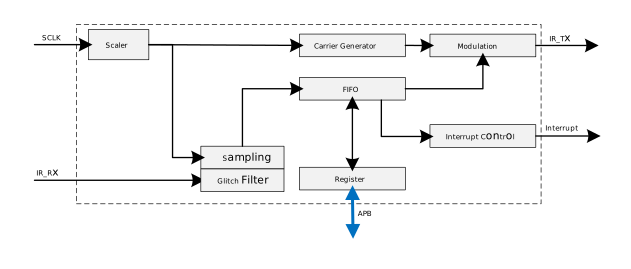
分频器(Scaler):基于 SCLK 分频,产生 Tx 载波频率或 Rx 采样频率。
载波发生器(Carrier Generator):生成 Tx 载波符号,支持灵活配置占空比。
调制器(Modulation):将空间符号调制为载波符号。
毛刺滤波器(Glitch Filter):在接收端滤除总线信号中的毛刺干扰。
FIFO
Tx FIFO:存储 Tx 载波符号计数值与数据状态。
Rx FIFO:缓存从总线接收的数据,供软件读取处理。
中断控制(Interrupt Control):向处理器产生中断事件。
寄存器(Register):用于配置 IR 模块参数。
工作原理
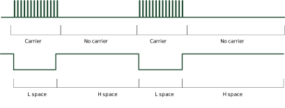
为简化 IR 信号模型,将一段 IR 信号划分为若干符号(Symbol)。符号的定义分为两类:一是在特定周期内包含若干载波时钟周期的信号,称为 载波符号 (Carrier Symbol);二是在特定周期内持续保持高电平或低电平的信号,称为 空间符号 (Space Symbol)。载波符号对应实际在空间中传播的信号,空间符号则对应调制前或解调后的基带信号。
发送模式
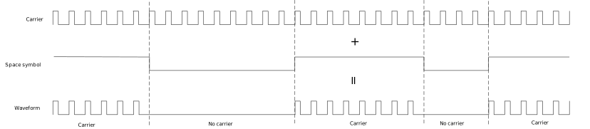
在 Tx 模式下,软件首先配置调制参数以生成固定频率的载波,然后将空间符号写入 Tx FIFO。Tx 模块自动完成调制并发送 IR 信号。IR Tx 流程如下图所示。
接收模式
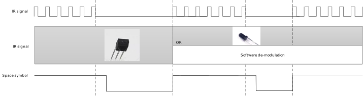
在 Rx 模式下,IR IP 以采样时钟为基准,测量输入信号连续高、低电平的脉宽周期,并将测量结果依次写入 Rx FIFO,供软件解析波形。IR IP 支持两种 Rx 前端:
红外接收器模块:载波已被前端模块滤除,输入信号为纯净的基带信号,IR IP 直接捕获空间符号,软件仅需解码。
红外二极管:输入信号仍携带载波,IR IP 捕获载波符号,软件需先解调再解码,会增加一定的 CPU 开销。
IR Rx 流程如下图所示。
功能描述
分频器
分频器是 IR 模块的时钟处理核心单元。分频器接收系统时钟 SCLK 作为输入,经过可编程分频后产生 IR 模块内部所需的各路时钟。通过配置 IR_CLK_DIV 寄存器的 IR_CLK_DIV 位域(12 位,寄存器 0x00[11:0]),可灵活设定分频系数:分频后时钟频率 = SCLK / (IR_CLK_DIV + 1)。
Tx 模式
在 Tx 模式下,分频器输出的时钟即为载波频率。载波发生器(Carrier Generator)基于该时钟生成占空比可调的载波符号,用于驱动 IR 发送。
例如,当 SCLK = 100 MHz、目标载波频率为 455 kHz 时,IR_CLK_DIV = (100M / 455k) - 1。
Rx 模式
在 Rx 模式下,分频器输出的时钟即为采样时钟。Rx 计数器以采样时钟为基准,对输入信号的高、低电平持续时间进行计数,测量结果写入 Rx FIFO,供软件解析波形。
例如,当 Rx 采样时钟为 10 MHz、Rx 计数值为 0x800000FF 时,表示高电平持续时间为 255μs(其中 bit[31] 表示输入电平:1 = 高电平,0 = 低电平)。
IR IP 的输入时钟(SCLK)频率因芯片而异:
默认时钟频率为 40 MHz。
默认时钟频率为 100 MHz。
默认时钟频率为 40 MHz。
默认时钟频率为 40 MHz。
发送模式
FIFO 格式
发送 IR 数据时,需要将数据写入 IR Tx FIFO 寄存器,因此了解其数据格式至关重要。发送前,应先将数据转换为 Tx FIFO 寄存器所定义的格式。Tx FIFO 寄存器为 32 位宽,各位定义如下:
- Bit[31]:
数据电平标志。1 = 高电平,0 = 低电平。
- Bit[30]:
数据结束标志。1 = 当前传输的最后一个包,0 = 普通包。
- Bit[29:28]:
Tx 补偿模式。00 = 使用 Tsample,11 = 使用 Tcomp_clk。
- Bit[27:0]:
载波周期数。
设 fcarrier表示载波频率(单位 Hz),Tduration表示载波符号或空间符号的持续时间(单位 μs)。则:
bit[27:0] = fcarrier× Tduration
FIFO 填充
以 NEC 协议为例,载波频率为 38 kHz。NEC 格式如下图所示,由 2 个起始符号、64 个数据符号和 1 个停止符号组成。
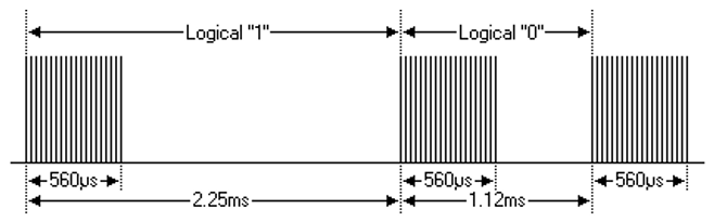
发送逻辑 '1',需向 Tx FIFO 寄存器写入两个字:
第一个字,bit[31] = 1,bit[30] = 0,bit[27:0] = 38 × 560 / 1000 = 21。
第二个字,bit[31] = 0,bit[30] = 0,bit[27:0] = 38 × (2250 - 560) / 1000 = 64。
发送逻辑 '0',需向 Tx FIFO 寄存器写入两个字:
第一个字,bit[31] = 1,bit[30] = 0,bit[27:0] = 38 × 560 / 1000 = 21。
第二个字,bit[31] = 0,bit[30] = 0,bit[27:0] = 38 × (1120 - 560) / 1000 = 21。
最后需要发送停止符号,此时应置 bit[30] = 1,表示当前传输结束。
补偿机制
大多数应用场景下无需启用补偿机制,若不涉及精度需求可跳过本节。
Tx 波形由若干载波符号和空间符号组成。软件依据协议规范(如 NEC)计算各符号的持续时间,但空间符号的持续时间通常无法被载波周期精确整除。若不加以补偿,误差将随符号累积。为此,IR Tx 引入了补偿机制以减小误差。
以 NEC 应用为例,下图展示了 Tx NEC 波形,其中 fcarrier= 38 kHz,duty = 1/3,系统时钟为 100 MHz。
对于 38kHz 载波频率:
Tcarrier= 1 / fcarrier= 1 / 38 k = 26.31μs
Tcarrier_duty= Tcarrier× duty = 8.77μs
补偿频率 fcomp 为独立时钟源,可自行设定所需频率。本例中设置 fcomp = 1MHz,因此:
Tcomp= 1 / fcomp= 1μs

Tx NEC 波形
将该波形划分为四个符号:560μs 载波符号、1690μs 空间符号(2250μs - 560μs)、560μs 载波符号和 560μs 空间符号(1120μs - 560μs)。对比以下两种计算方式可以看出,使用补偿机制后精度明显提升。
项目 |
普通 Tx (IR_TX_COMPENSATION = 0) |
Tx 补偿 (IR_TX_COMPENSATION = 3) |
|---|---|---|
第 1 周期 |
560μs ≈ 21 × 26.31 + 8.77 = 561.26μs |
560μs ≈ 21 × 26.31 + 8.77 = 561.26μs |
第 2 周期 |
1690μs ≈ 64 × 26.31 + (26.31 - 8.77) = 1701.38μs |
1690μs ≈ (26.31 - 8.77) + 1673 × 1 = 1690.54μs |
第 3 周期 |
560μs ≈ 21 × 26.31 + 8.77 = 561.26μs |
560μs ≈ 21 × 26.31 + 8.77 = 561.26μs |
第 4 周期 |
560μs ≈ 21 × 26.31 + (26.31 - 8.77) = 570.05μs |
560μs ≈ (26.31 - 8.77) + 543 × 1 = 560.54μs |
Tx FIFO 数据值 |
0x80000015, 0x00000040; 0x80000015, 0x00000015 |
0x80000015, 0x30000689; 0x80000015, 0x3000021F |
备注
补偿机制仅适用于空间符号。
不建议使用补偿模式中的 IR_TX_COMPENSATION = 1 和 IR_TX_COMPENSATION = 2。如需启用补偿,请使用 IR_TX_COMPENSATION = 3 模式。
若启用了
IR_TX_DE_INVERSE,请确保 Tx 补偿分频器 IR_TX_COMPE_DIV 的IR_TX_COMPE_DIV(寄存器 0xC[11:0]) 不小于 Tx 占空比计数值 IR_TX_CONFIG 的IR_TX_DUTY_NUM(寄存器 0x4[27:16])。
接收模式
FIFO 格式
接收 IR 数据时,需从 Rx FIFO 寄存器中读取数据,因此了解其数据格式至关重要。Rx FIFO 寄存器为 32 位宽,各位定义如下:
Bit[31] 表示数据电平。1 = 高电平,0 = 低电平。
Bit[30:0] 存储接收到的数据,以采样周期数表示电平持续时间。
设 fsampling 表示采样频率(单位 kHz),Tlevel 表示对应高/低电平的持续时间(单位 μs)。则:
Tlevel= bit[30:0] / fsampling× 1000
软件可根据 Tlevel 进一步解析红外协议并提取所需信息。
接收启动
支持自动启动和手动启动两种方式,由 IR_RX_CONFIG 的 IR_RX_START_MODE (寄存器 0x18[27]) 控制。
自动启动
设置 IR_RX_START_MODE = 1 进入自动接收模式。在该模式下,当 Rx 输入信号满足预设的触发条件时,硬件自动开始接收。触发类型通过 IR_RX_TRIGGER_MODE 配置:
值 |
触发类型 |
说明 |
|---|---|---|
00 |
IR_RX_FALL_EDGE |
检测到下降沿(高电平→低电平)时触发 |
01 |
IR_RX_RISING_EDGE |
检测到上升沿(低电平→高电平)时触发 |
10 |
IR_RX_DOUBLE_EDGE |
检测到任意电平跳变(上升沿或下降沿)时触发 |
使能 Rx 模块后,硬件自动等待触发条件,无需软件干预。
手动启动
设置 IR_RX_START_MODE = 0 进入手动接收模式。在该模式下,软件通过向 IR_RX_CONFIG 的 IR_RX_MAN_START (寄存器 0x18[28]) 写 1 来启动接收,适用于需要精确控制接收起点的场景。
接收终止
Rx 模块通过计数器阈值中断判定接收终止。当输入信号中某一电平的持续时间超过预设阈值时,触发 IR_RX_CNT_THR_INT_STATUS 中断,表示一次完整的 IR 接收结束。
终止条件由以下寄存器设置共同决定:
终止电平类型 (
IR_RX_CNT_THR_TRIGGER_LV):0:当低电平持续时间 ≥ 阈值时触发中断
1:当高电平持续时间 ≥ 阈值时触发中断
计数阈值 (
IR_RX_CNT_THR):31 位阈值,持续时间 = 阈值 / 采样频率。使能中断:必须使能
IR_RX_CNT_THR_INT_EN,方可在条件满足时收到中断通知。
备注
阈值应根据应用场景中 IR 信号的特点进行配置。两个 IR 数据帧之间的间隔时间通常大于单次传输中任意电平的持续时间,因此将该间隔时间设为阈值,可靠地区分数据帧。
接收滤波器
IR Rx 输入端内置毛刺滤波器,可在采样前滤除窄脉冲干扰。滤波宽度通过 IR_RX_CONFIG 的 IR_RX_FILTER_STAGETX (寄存器 0x18[23:21]) 进行配置。各芯片的滤波宽度映射如下:
滤波宽度可选:50ns、75ns、100ns、125ns、150ns、175ns、200ns、225ns。
滤波宽度可选:20ns、30ns、40ns、50ns、60ns、70ns、80ns、90ns。
滤波宽度可选:50ns、75ns、100ns、125ns、150ns、175ns、200ns、225ns。
滤波宽度可选:50ns、75ns、100ns、125ns、150ns、175ns、200ns、225ns。
中断
每种模式下支持的中断标志如下所列,各中断源均可单独使能、屏蔽或清除。
模式 |
中断标志 |
描述 |
|---|---|---|
Tx 模式 |
IR_TX_FIFO_OVER_INT |
Tx FIFO 已满时,再次写入数据触发此中断。 |
IR_TX_FIFO_LEVEL_INT |
Tx FIFO 使用量从阈值降至阈值 - 1 时触发此中断。 |
|
IR_TX_FIFO_EMPTY_INT |
Tx FIFO 使用量从 1 降至 0(即 FIFO 为空)时触发此中断。 |
|
Rx 模式 |
IR_RX_FIFO_ERROR_INT |
Rx FIFO 为空时,尝试读取数据触发此中断。 |
IR_RX_CNT_THR_INT |
输入电平持续时间超过 Rx 计数器阈值时触发此中断。 |
|
IR_RX_CNT_OF_INT |
Rx 计数器溢出且未触发 IR_RX_CNT_THR_INT 时触发此中断。 |
|
IR_RX_FIFO_OF_INT |
Rx FIFO 已满时,仍从 IR 输入引脚接收到新数据触发此中断。 |
|
IR_RX_FIFO_LEVEL_INT |
Rx FIFO 使用量从阈值升至阈值 + 1 时触发此中断。 |
|
IR_RX_FIFO_FULL_INT |
Rx FIFO 写满时触发此中断。 |
寄存器
Base Address: 0x41107000
Name |
Address offset |
Access |
Description |
|---|---|---|---|
000h |
R/W |
||
004h |
R/W |
||
008h |
R |
||
00Ch |
R/W |
||
010h |
R/W |
||
014h |
R/W |
||
018h |
R/W |
||
01Ch |
R |
||
020h |
R/W |
||
024h |
R/W |
||
028h |
R |
||
02Ch |
R |
||
030h |
R |
REG_IR_CLK_DIV
Name: IR clock division register
Size: 32
Address offset: 000h
Read/write access: R/W
Bit |
Symbol |
Access |
INI |
Description |
|---|---|---|---|---|
31:12 |
RSVD |
R |
- |
Reserved |
11:0 |
IR_CLK_DIV |
R/W |
0x0 |
IR_CLK = IO_CLK/(1 + IR_CLK_DIV)
For example: sys_clk = 100MHz, modulation_freq = 455kHz, IR_DIV_NUM = (sys_clk/modulation_freq) - 1
IR_DIV_NUM = (sys_clk/sample clock) - 1 For example: sample clock = 100MHz, IR_DIV_NUM = 0; sample clock = 50MHz, IR_DIV_NUM = 1 |
REG_IR_TX_CONFIG
Name: IR Tx configuration register
Size: 32
Address offset: 004h
Read/write access: R/W
Bit |
Symbol |
Access |
INI |
Description |
|---|---|---|---|---|
31 |
IR_MODE_SEL |
R/W |
0x0 |
|
30 |
IR_TX_START |
R/W |
0x0 |
|
29:28 |
RSVD |
R |
- |
Reserved |
27:16 |
IR_TX_DUTY_NUM |
R/W |
0x0 |
Duty cycle setting for modulation frequency For example: for 1/3 duty cycle, IR_DUTY_NUM = (IR_DIV_NUM+1)/3 备注 Set this value equal to IR_DIV_NUM to generate 100% duty waveform. |
15 |
RSVD |
R |
- |
Reserved |
14 |
IR_TX_OUTPUT_INVERSE |
R/W |
0x0 |
|
13 |
IR_TX_DE_INVERSE |
R/W |
0x0 |
|
12:8 |
IR_TX_FIFO_LEVEL_TH |
R/W |
0x0 |
Tx FIFO interrupt threshold. When Tx FIFO depth = < threshold value, interrupt is triggered. |
7 |
RSVD |
R |
- |
Reserved |
6 |
IR_TX_IDLE_STATE |
R/W |
0x0 |
Tx output state in idle
|
5 |
IR_TX_FIFO_OVER_INT_MASK |
R/W |
0x0 |
Tx FIFO overflow interrupt
|
4 |
IR_TX_FIFO_OVER_INT_EN |
R/W |
0x0 |
Tx FIFO overflow interrupt
|
3 |
IR_TX_FIFO_LEVEL_INT_MASK |
R/W |
0x0 |
Tx FIFO level interrupt
|
2 |
IR_TX_FIFO_EMPTY_INT_MASK |
R/W |
0x0 |
Tx FIFO empty interrupt
|
1 |
IR_TX_FIFO_LEVEL_INT_EN |
R/W |
0x0 |
Tx FIFO level interrupt When Tx FIFO offset <= threshold value, interrupt is triggered.
|
0 |
IR_TX_FIFO_EMPTY_INT_EN |
R/W |
0x0 |
Tx FIFO empty interrupt
|
REG_IR_TX_SR
Name: IR Tx FIFO and interrupt status register
Size: 32
Address offset: 008h
Read/write access: R
Bit |
Symbol |
Access |
INI |
Description |
|---|---|---|---|---|
31:16 |
RSVD |
R |
- |
Reserved |
15 |
IR_TX_FIFO_EMPTY |
R |
0x0 |
|
14 |
IR_TX_FIFO_FULL |
R |
0x0 |
|
13:8 |
IR_TX_FIFO_OFFSET |
R |
0x0 |
Tx FIFO offset is from 0 to 32. 备注 After Tx last packet, hardware can't clear Tx FIFO offset. |
7:5 |
RSVD |
R |
- |
Reserved |
4 |
IR_TX_STATUS |
R |
0x0 |
|
3 |
RSVD |
R |
- |
Reserved |
2 |
IR_TX_FIFO_OVER_INT_STATUS |
R |
0x0 |
Tx FIFO overflow interrupt
|
1 |
IR_TX_FIFO_LEVEL_INT_STATUS |
R |
0x0 |
When Tx FIFO offset <= threshold value, interrupt is triggered.
|
0 |
IR_TX_FIFO_EMPTY_INT_STATUS |
R |
0x0 |
Tx FIFO empty interrupt
|
REG_IR_TX_COMPE_DIV
Name: IR Tx compensation division register
Size: 32
Address offset: 00Ch
Read/write access: R/W
Bit |
Symbol |
Access |
INI |
Description |
|---|---|---|---|---|
31:12 |
RSVD |
R |
- |
Reserved |
11:0 |
TX_COMPE_DIV |
R/W |
0x0 |
IR_TX_CLK_Period = SCLK/(TX_COMPE_DIV + 1) |
REG_IR_TX_INT_CLR
Name: IR Tx FIFO and interrupt clear register
Size: 32
Address offset: 010h
Read/write access: R/W
Bit |
Symbol |
Access |
INI |
Description |
|---|---|---|---|---|
31:4 |
RSVD |
R |
- |
Reserved |
3 |
IR_TX_FIFO_OVER_INT_CLR |
R/W |
Tx FIFO overflow interrupt Write 1 to clear |
|
2 |
IR_TX_FIFO_LEVEL_INT_CLR |
R/W |
When Tx FIFO offset <= threshold value, interrupt is triggered. Write 1 to clear |
|
1 |
IR_TX_FIFO_EMPTY_INT_CLR |
R/W |
Tx FIFO empty interrupt Write 1 to clear |
|
0 |
IR_TX_FIFO_CLR |
R/W |
Write 1 to clear Tx FIFO |
REG_IR_TX_FIFO
Name: IR Tx FIFO register
Size: 32
Address offset: 014h
Read/write access: R/W
Bit |
Symbol |
Access |
INI |
Description |
|---|---|---|---|---|
31 |
IR_TX_DATA_TYPE |
R/W |
0 |
Data type
|
30 |
IR_TX_DATA_END_FLAG |
R/W |
0 |
|
29:28 |
IR_TX_COMPENSATION |
R/W |
0 |
|
27:0 |
IR_TX_DATA_TIME |
R/W |
0 |
Real active time = (IR_TX_DATA_TIME + 1) * IR_TX_CLK_Period |
REG_IR_RX_CONFIG
Name: IR Rx configuration register
Size: 32
Address offset: 018h
Read/write access: R/W
Bit |
Symbol |
Access |
INI |
Description |
|---|---|---|---|---|
31:29 |
RSVD |
R |
- |
Reserved |
28 |
IR_RX_START |
R/W |
0x0 |
|
27 |
IR_RX_START_MODE |
R/W |
0x0 |
|
26 |
IR_RX_MAN_START |
R/W |
0x0 |
If IR_RX_TRIGGER_MODE =0, writing 1 means starting to check the waveform. |
25:24 |
IR_RX_TRIGGER_MODE |
R/W |
0x0 |
|
23:21 |
IR_RX_FILTER_STAGETX |
R/W |
0x0 |
… |
20 |
RSVD |
R |
- |
Reserved |
19 |
IR_RX_FIFO_ERROR_INT_MASK |
R/W |
0x0 |
Rx FIFO error read interrupt When Rx FIFO is empty, read Rx FIFO and trigger interrupt.
|
18 |
IR_RX_CNT_THR_INT_MASK |
R/W |
0x0 |
Rx count threshold interrupt
|
17 |
IR_RX_FIFO_OF_INT_MASK |
R/W |
0x0 |
Rx FIFO overflow
|
16 |
IR_RX_CNT_OF_INT_MASK |
R/W |
0x0 |
RX counter overflow
|
15 |
IR_RX_FIFO_LEVEL_INT_MASK |
R/W |
0x0 |
Rx FIFO level interrupt
When Rx FIFO offset >= threshold value, this interrupt is triggered. |
14 |
IR_RX_FIFO_FULL_INT_MASK |
R/W |
0x0 |
Rx FIFO full interrupt
|
13 |
IR_RX_FIFO_DISCARD_SET |
R/W |
0x0 |
When FIFO is full, new data is send to FIFO.
|
12:8 |
IR_RX_FIFO_LEVEL_TH |
R/W |
0x0 |
Rx FIFO interrupt threshold When Rx FIFO depth > threshold value, this interrupt is triggered. |
7:6 |
RSVD |
R |
- |
Reserved |
5 |
IR_RX_FIFO_ERROR_INT_EN |
R/W |
0x0 |
Rx FIFO error read interrupt When Rx FIFO is empty, reading the Rx FIFO triggers this interrupt.
|
4 |
IR_RX_CNT_THR_INT_EN |
R/W |
0x0 |
Rx count threshold interrupt
|
3 |
IR_RX_FIFO_OF_INT_EN |
R/W |
0x0 |
RX FIFO overflow
|
2 |
IR_RX_CNT_OF_INT_EN |
R/W |
0x0 |
RX counter overflow
|
1 |
IR_RX_FIFO_LEVEL_INT_EN |
R/W |
0x0 |
Rx FIFO level interrupt When Rx FIFO offset >= threshold value, this interrupt is triggered.
|
0 |
IR_RX_FIFO_FULL_INT_EN |
R/W |
0x0 |
Rx FIFO full interrupt
|
REG_IR_RX_SR
Name: IR Rx FIFO and interrupt status register
Size: 32
Address offset: 01Ch
Read/write access: R
Bit |
Symbol |
Access |
INI |
Description |
|---|---|---|---|---|
31:18 |
RSVD |
R |
- |
Reserved |
17 |
IR_RX_FIFO_EMPTY |
R |
0x0 |
|
16 |
IR_RX_FIFO_FULL |
R |
0x0 |
|
15:14 |
RSVD |
R |
- |
Reserved |
13:8 |
IR_RX_FIFO_OFFSET |
R |
0x0 |
Rx FIFO offset |
7 |
IR_RX_STATE |
R |
0x0 |
|
6 |
RSVD |
R |
- |
Reserved |
5 |
IR_RX_FIFO_ERROR_INT_STATUS |
R |
0x0 |
Rx FIFO error read interrupt status When Rx FIFO is empty, reading the Rx FIFO triggers this interrupt.
|
4 |
IR_RX_CNT_THR_INT_STATUS |
R |
0x0 |
Rx count threshold interrupt status
|
3 |
IR_RX_FIFO_OF_INT_STATUS |
R |
0x0 |
Rx FIFO overflow interrupt status
|
2 |
IR_RX_CNT_OF_INT_STATUS |
R |
0x0 |
Rx counter overflow interrupt status
|
1 |
IR_RX_FIFO_LEVEL_INT_STATUS |
R |
0x0 |
Rx FIFO level interrupt status
|
0 |
IR_RX_FIFO_FULL_INT_STATUS |
R |
0x0 |
Rx FIFO full interrupt status
|
REG_IR_RX_INT_CLR
Name: IR Rx FIFO and interrupt clear register
Size: 32
Address offset: 020h
Read/write access: R/W
Bit |
Symbol |
Access |
INI |
Description |
|---|---|---|---|---|
31:9 |
RSVD |
R |
- |
Reserved |
8 |
IR_RX_FIFO_CLR |
R/W |
Write 1 to clear Rx FIFO |
|
7:6 |
RSVD |
R |
- |
Reserved |
5 |
IR_RX_FIFO_ERROR_INT_CLR |
R/W |
Rx FIFO error read interrupt Write 1 to clear |
|
4 |
IR_RX_CNT_THR_INT_CLR |
R/W |
Rx count threshold interrupt Write 1 to clear |
|
3 |
IR_RX_FIFO_OF_INT_CLR |
R/W |
Rx FIFO overflow interrupt Write 1 to clear |
|
2 |
IR_RX_CNT_OF_INT_CLR |
R/W |
Rx counter overflow interrupt Write 1 to clear |
|
1 |
IR_RX_FIFO_LEVEL_INT_CLR |
R/W |
Rx FIFO level interrupt Write 1 to clear |
|
0 |
IR_RX_FIFO_FULL_INT_CLR |
R/W |
Rx FIFO full interrupt Write 1 to clear |
REG_IR_RX_CNT_INT_SEL
Name: IR Rx count threshold configure register
Size: 32
Address offset: 024h
Read/write access: R/W
Bit |
Symbol |
Access |
INI |
Description |
|---|---|---|---|---|
31 |
IR_RX_CNT_THR_TRIGGER_LV |
R/W |
0x0 |
Trigger level
|
30:0 |
IR_RX_CNT_THR |
R/W |
0x0 |
31-bits threshold |
REG_IR_RX_FIFO
Name: IR Rx FIFO register
Size: 32
Address offset: 028h
Read/write access: R
Bit |
Symbol |
Access |
INI |
Description |
|---|---|---|---|---|
31 |
IR_RX_LEVEL |
R |
0x0 |
Rx Level
|
30:0 |
IR_RX_CNT |
R |
0x0 |
31 bits cycle duration |
REG_IR_VERSION
Name: IR version register
Size: 32
Address offset: 02Ch
Read/write access: R
Bit |
Symbol |
Access |
INI |
Description |
|---|---|---|---|---|
31:0 |
IR_VERSION |
R |
0x1410150A |
IR IP version |
REG_IR_DUMMY
Name: IR Dummy Register
Size: 32
Address offset: 030h
Read/write access: R
Bit |
Symbol |
Access |
INI |
Description |
|---|---|---|---|---|
31:16 |
RSVD |
R |
- |
Reserved |
15:0 |
DUMMY |
R |
0x0 |
Reserved for HW |
Base Address: 0x400EE000
Name |
Address offset |
Access |
Description |
|---|---|---|---|
000h |
R/W |
||
004h |
R/W |
||
008h |
R |
||
00Ch |
R/W |
||
010h |
R/W |
||
014h |
R/W |
||
018h |
R/W |
||
01Ch |
R |
||
020h |
R/W |
||
024h |
R/W |
||
028h |
R |
||
02Ch |
R |
REG_IR_CLK_DIV
Name: IR clock division register
Size: 32
Address offset: 000h
Read/write access: R/W
Bit |
Symbol |
Access |
INI |
Description |
|---|---|---|---|---|
31:12 |
RSVD |
R |
- |
Reserved |
11:0 |
IR_CLK_DIV |
R/W |
0x0 |
IR_CLK = IO_CLK/(1 + IR_CLK_DIV)
For example: sys_clk = 100MHz, modulation_freq = 455kHz, IR_DIV_NUM = (sys_clk/modulation_freq) - 1
IR_DIV_NUM = (sys_clk/sample clock) - 1 For example: sample clock = 100MHz, IR_DIV_NUM = 0; sample clock = 50MHz, IR_DIV_NUM = 1 |
REG_IR_TX_CONFIG
Name: IR Tx configuration register
Size: 32
Address offset: 004h
Read/write access: R/W
Bit |
Symbol |
Access |
INI |
Description |
|---|---|---|---|---|
31 |
IR_MODE_SEL |
R/W |
0x0 |
|
30 |
IR_TX_START |
R/W |
0x0 |
|
29:28 |
RSVD |
R |
- |
Reserved |
27:16 |
IR_TX_DUTY_NUM |
R/W |
0x0 |
Duty cycle setting for modulation frequency For example: for 1/3 duty cycle, IR_DUTY_NUM = (IR_DIV_NUM+1)/3 备注 Set this value equals to IR_DIV_NUM to generate 100% duty waveform. |
15 |
RSVD |
R |
- |
Reserved |
14 |
IR_TX_OUTPUT_INVERSE |
R/W |
0x0 |
|
13 |
IR_TX_DE_INVERSE |
R/W |
0x0 |
|
12:8 |
IR_TX_FIFO_LEVEL_TH |
R/W |
0x0 |
Tx FIFO interrupt threshold. When Tx FIFO depth = < threshold value, interrupt is triggered. |
7 |
RSVD |
R |
- |
Reserved |
6 |
IR_TX_IDLE_STATE |
R/W |
0x0 |
Tx output state in idle
|
5 |
IR_TX_FIFO_OVER_INT_MASK |
R/W |
0x0 |
Tx FIFO overflow interrupt
|
4 |
IR_TX_FIFO_OVER_INT_EN |
R/W |
0x0 |
Tx FIFO overflow interrupt
|
3 |
IR_TX_FIFO_LEVEL_INT_MASK |
R/W |
0x0 |
Tx FIFO level interrupt
|
2 |
IR_TX_FIFO_EMPTY_INT_MASK |
R/W |
0x0 |
Tx FIFO empty interrupt
|
1 |
IR_TX_FIFO_LEVEL_INT_EN |
R/W |
0x0 |
Tx FIFO level interrupt When Tx FIFO offset <= threshold value, interrupt is triggered.
|
0 |
IR_TX_FIFO_EMPTY_INT_EN |
R/W |
0x0 |
Tx FIFO empty interrupt
|
REG_IR_TX_SR
Name: IR Tx FIFO and interrupt status register
Size: 32
Address offset: 008h
Read/write access: R
Bit |
Symbol |
Access |
INI |
Description |
|---|---|---|---|---|
31:16 |
RSVD |
R |
- |
Reserved |
15 |
IR_TX_FIFO_EMPTY |
R |
0x0 |
|
14 |
IR_TX_FIFO_FULL |
R |
0x0 |
|
13:8 |
IR_TX_FIFO_OFFSET |
R |
0x0 |
Tx FIFO offset is from 0 to 32. 备注 After Tx last packet, hardware can't clear Tx FIFO offset. |
7:5 |
RSVD |
R |
- |
Reserved |
4 |
IR_TX_STATUS |
R |
0x0 |
|
3 |
RSVD |
R |
- |
Reserved |
2 |
IR_TX_FIFO_OVER_INT_STATUS |
R |
0x0 |
Tx FIFO overflow interrupt
|
1 |
IR_TX_FIFO_LEVEL_INT_STATUS |
R |
0x0 |
When Tx FIFO offset <= threshold value, interrupt is triggered.
|
0 |
IR_TX_FIFO_EMPTY_INT_STATUS |
R |
0x0 |
Tx FIFO empty interrupt
|
REG_IR_TX_COMPE_DIV
Name: IR Tx compensation division register
Size: 32
Address offset: 00Ch
Read/write access: R/W
Bit |
Symbol |
Access |
INI |
Description |
|---|---|---|---|---|
31:12 |
RSVD |
R |
- |
Reserved |
11:0 |
TX_COMPE_DIV |
R/W |
0x0 |
IR_TX_CLK_Period = SCLK/(TX_COMPE_DIV + 1) |
REG_IR_TX_INT_CLR
Name: IR Tx FIFO and interrupt clear register
Size: 32
Address offset: 010h
Read/write access: R/W
Bit |
Symbol |
Access |
INI |
Description |
|---|---|---|---|---|
31:4 |
RSVD |
R |
- |
Reserved |
3 |
IR_TX_FIFO_OVER_INT_CLR |
R/W |
Tx FIFO overflow interrupt Write 1 to clear |
|
2 |
IR_TX_FIFO_LEVEL_INT_CLR |
R/W |
When Tx FIFO offset <= threshold value, interrupt is triggered. Write 1 to clear |
|
1 |
IR_TX_FIFO_EMPTY_INT_CLR |
R/W |
Tx FIFO empty interrupt Write 1 to clear |
|
0 |
IR_TX_FIFO_CLR |
R/W |
Write 1 to clear Tx FIFO |
REG_IR_TX_FIFO
Name: IR Tx FIFO register
Size: 32
Address offset: 014h
Read/write access: R/W
Bit |
Symbol |
Access |
INI |
Description |
|---|---|---|---|---|
31 |
IR_TX_DATA_TYPE |
R/W |
0 |
Data type
|
30 |
IR_TX_DATA_END_FLAG |
R/W |
0 |
|
29:28 |
IR_TX_COMPENSATION |
R/W |
0 |
|
27:0 |
IR_TX_DATA_TIME |
R/W |
0 |
Real active time = (IR_TX_DATA_TIME + 1) * IR_TX_CLK_Period |
REG_IR_RX_CONFIG
Name: IR Rx configuration register
Size: 32
Address offset: 018h
Read/write access: R/W
Bit |
Symbol |
Access |
INI |
Description |
|---|---|---|---|---|
31:29 |
RSVD |
R |
- |
Reserved |
28 |
IR_RX_START |
R/W |
0x0 |
|
27 |
IR_RX_START_MODE |
R/W |
0x0 |
|
26 |
IR_RX_MAN_START |
R/W |
0x0 |
If IR_RX_TRIGGER_MODE =0, writing 1 means starting to check the waveform. |
25:24 |
IR_RX_TRIGGER_MODE |
R/W |
0x0 |
|
23:21 |
IR_RX_FILTER_STAGETX |
R/W |
0x0 |
… |
20 |
RSVD |
R |
- |
Reserved |
19 |
IR_RX_FIFO_ERROR_INT_MASK |
R/W |
0x0 |
Rx FIFO error read interrupt When Rx FIFO is empty, read Rx FIFO and trigger interrupt.
|
18 |
IR_RX_CNT_THR_INT_MASK |
R/W |
0x0 |
Rx count threshold interrupt
|
17 |
IR_RX_FIFO_OF_INT_MASK |
R/W |
0x0 |
Rx FIFO overflow
|
16 |
IR_RX_CNT_OF_INT_MASK |
R/W |
0x0 |
RX counter overflow
|
15 |
IR_RX_FIFO_LEVEL_INT_MASK |
R/W |
0x0 |
Rx FIFO level interrupt
When Rx FIFO offset >= threshold value, this interrupt is triggered. |
14 |
IR_RX_FIFO_FULL_INT_MASK |
R/W |
0x0 |
Rx FIFO full interrupt
|
13 |
IR_RX_FIFO_DISCARD_SET |
R/W |
0x0 |
When FIFO is full, new data is send to FIFO.
|
12:8 |
IR_RX_FIFO_LEVEL_TH |
R/W |
0x0 |
Rx FIFO interrupt threshold When Rx FIFO depth > threshold value, this interrupt is triggered. |
7:6 |
RSVD |
R |
- |
Reserved |
5 |
IR_RX_FIFO_ERROR_INT_EN |
R/W |
0x0 |
Rx FIFO error read interrupt When Rx FIFO is empty, reading the Rx FIFO triggers this interrupt.
|
4 |
IR_RX_CNT_THR_INT_EN |
R/W |
0x0 |
Rx count threshold interrupt
|
3 |
IR_RX_FIFO_OF_INT_EN |
R/W |
0x0 |
RX FIFO overflow
|
2 |
IR_RX_CNT_OF_INT_EN |
R/W |
0x0 |
RX counter overflow
|
1 |
IR_RX_FIFO_LEVEL_INT_EN |
R/W |
0x0 |
Rx FIFO level interrupt When Rx FIFO offset >= threshold value, this interrupt is triggered.
|
0 |
IR_RX_FIFO_FULL_INT_EN |
R/W |
0x0 |
Rx FIFO full interrupt
|
REG_IR_RX_SR
Name: IR Rx FIFO and interrupt status register
Size: 32
Address offset: 01Ch
Read/write access: R
Bit |
Symbol |
Access |
INI |
Description |
|---|---|---|---|---|
31:18 |
RSVD |
R |
- |
Reserved |
17 |
IR_RX_FIFO_EMPTY |
R |
0x0 |
|
16 |
IR_RX_FIFO_FULL |
R |
0x0 |
|
15:14 |
RSVD |
R |
- |
Reserved |
13:8 |
IR_RX_FIFO_OFFSET |
R |
0x0 |
Rx FIFO offset |
7 |
IR_RX_STATE |
R |
0x0 |
|
6 |
RSVD |
R |
- |
Reserved |
5 |
IR_RX_FIFO_ERROR_INT_STATUS |
R |
0x0 |
Rx FIFO error read interrupt status When Rx FIFO is empty, reading the Rx FIFO triggers this interrupt.
|
4 |
IR_RX_CNT_THR_INT_STATUS |
R |
0x0 |
Rx count threshold interrupt status
|
3 |
IR_RX_FIFO_OF_INT_STATUS |
R |
0x0 |
Rx FIFO overflow interrupt status
|
2 |
IR_RX_CNT_OF_INT_STATUS |
R |
0x0 |
Rx counter overflow interrupt status
|
1 |
IR_RX_FIFO_LEVEL_INT_STATUS |
R |
0x0 |
Rx FIFO level interrupt status
|
0 |
IR_RX_FIFO_FULL_INT_STATUS |
R |
0x0 |
Rx FIFO full interrupt status
|
REG_IR_RX_INT_CLR
Name: IR Rx FIFO and interrupt clear register
Size: 32
Address offset: 020h
Read/write access: R/W
Bit |
Symbol |
Access |
INI |
Description |
|---|---|---|---|---|
31:9 |
RSVD |
R |
- |
Reserved |
8 |
IR_RX_FIFO_CLR |
R/W |
Write 1 to clear Rx FIFO |
|
7:6 |
RSVD |
R |
- |
Reserved |
5 |
IR_RX_FIFO_ERROR_INT_CLR |
R/W |
Rx FIFO error read interrupt Write 1 to clear |
|
4 |
IR_RX_CNT_THR_INT_CLR |
R/W |
Rx count threshold interrupt Write 1 to clear |
|
3 |
IR_RX_FIFO_OF_INT_CLR |
R/W |
Rx FIFO overflow interrupt Write 1 to clear |
|
2 |
IR_RX_CNT_OF_INT_CLR |
R/W |
Rx counter overflow interrupt Write 1 to clear |
|
1 |
IR_RX_FIFO_LEVEL_INT_CLR |
R/W |
Rx FIFO level interrupt Write 1 to clear |
|
0 |
IR_RX_FIFO_FULL_INT_CLR |
R/W |
Rx FIFO full interrupt Write 1 to clear |
REG_IR_RX_CNT_INT_SEL
Name: IR Rx count threshold configure register
Size: 32
Address offset: 024h
Read/write access: R/W
Bit |
Symbol |
Access |
INI |
Description |
|---|---|---|---|---|
31 |
IR_RX_CNT_THR_TRIGGER_LV |
R/W |
0x0 |
Trigger level
|
30:0 |
IR_RX_CNT_THR |
R/W |
0x0 |
31-bits threshold |
REG_IR_RX_FIFO
Name: IR Rx FIFO register
Size: 32
Address offset: 028h
Read/write access: R
Bit |
Symbol |
Access |
INI |
Description |
|---|---|---|---|---|
31 |
IR_RX_LEVEL |
R |
0x0 |
Rx Level
|
30:0 |
IR_RX_CNT |
R |
0x0 |
31-bits cycle duration |
REG_IR_VERSION
Name: IR IP version register
Size: 32
Address offset: 02Ch
Read/write access: R
Bit |
Symbol |
Access |
INI |
Description |
|---|---|---|---|---|
31:0 |
IR_VERSION |
R |
0x1410150A |
IR IP version |
Base Address: 0x41007000
Name |
Address offset |
Access |
Description |
|---|---|---|---|
000h |
R/W |
||
004h |
R/W |
||
008h |
R |
||
00Ch |
R/W |
||
010h |
R/W |
||
014h |
R/W |
||
018h |
R/W |
||
01Ch |
R |
||
020h |
R/W |
||
024h |
R/W |
||
028h |
R |
||
02Ch |
R |
||
030h |
R |
REG_IR_CLK_DIV
Name: IR clock division register
Size: 32
Address offset: 000h
Read/write access: R/W
Bit |
Symbol |
Access |
INI |
Description |
|---|---|---|---|---|
31:12 |
RSVD |
R |
- |
Reserved |
11:0 |
IR_CLK_DIV |
R/W |
0x0 |
IR_CLK = IO_CLK/(1 + IR_CLK_DIV)
For example: sys_clk = 40MHz, modulation_freq = 455kHz, IR_DIV_NUM = (sys_clk/modulation_freq) - 1
IR_DIV_NUM = (sys_clk/sample clock) - 1 For example: sample clock = 40MHz, IR_DIV_NUM = 0; sample clock = 20MHz, IR_DIV_NUM = 1 |
REG_IR_TX_CONFIG
Name: IR Tx configuration register
Size: 32
Address offset: 004h
Read/write access: R/W
Bit |
Symbol |
Access |
INI |
Description |
|---|---|---|---|---|
31 |
IR_MODE_SEL |
R/W |
0x0 |
|
30 |
IR_TX_START |
R/W |
0x0 |
|
29:28 |
RSVD |
R |
- |
Reserved |
27:16 |
IR_TX_DUTY_NUM |
R/W |
0x0 |
Duty cycle setting for modulation frequency For example: for 1/3 duty cycle, IR_DUTY_NUM = (IR_DIV_NUM+1)/3 备注 Set this value equals to IR_DIV_NUM to generate 100% duty waveform. |
15 |
RSVD |
R |
- |
Reserved |
14 |
IR_TX_OUTPUT_INVERSE |
R/W |
0x0 |
|
13 |
IR_TX_DE_INVERSE |
R/W |
0x0 |
|
12:8 |
IR_TX_FIFO_LEVEL_TH |
R/W |
0x0 |
Tx FIFO interrupt threshold. When Tx FIFO depth = < threshold value, interrupt is triggered. |
7 |
RSVD |
R |
- |
Reserved |
6 |
IR_TX_IDLE_STATE |
R/W |
0x0 |
Tx output state in idle
|
5 |
IR_TX_FIFO_OVER_INT_MASK |
R/W |
0x0 |
Tx FIFO overflow interrupt
|
4 |
IR_TX_FIFO_OVER_INT_EN |
R/W |
0x0 |
Tx FIFO overflow interrupt
|
3 |
IR_TX_FIFO_LEVEL_INT_MASK |
R/W |
0x0 |
Tx FIFO level interrupt
|
2 |
IR_TX_FIFO_EMPTY_INT_MASK |
R/W |
0x0 |
Tx FIFO empty interrupt
|
1 |
IR_TX_FIFO_LEVEL_INT_EN |
R/W |
0x0 |
Tx FIFO level interrupt When Tx FIFO offset <= threshold value, interrupt is triggered.
|
0 |
IR_TX_FIFO_EMPTY_INT_EN |
R/W |
0x0 |
Tx FIFO empty interrupt
|
REG_IR_TX_SR
Name: IR Tx FIFO and interrupt status register
Size: 32
Address offset: 008h
Read/write access: R
Bit |
Symbol |
Access |
INI |
Description |
|---|---|---|---|---|
31:16 |
RSVD |
R |
- |
Reserved |
15 |
IR_TX_FIFO_EMPTY |
R |
0x0 |
|
14 |
IR_TX_FIFO_FULL |
R |
0x0 |
|
13:8 |
IR_TX_FIFO_OFFSET |
R |
0x0 |
Tx FIFO offset is from 0 to 32. 备注 After Tx last packet, hardware can't clear Tx FIFO offset. |
7:5 |
RSVD |
R |
- |
Reserved |
4 |
IR_TX_STATUS |
R |
0x0 |
|
3 |
RSVD |
R |
- |
Reserved |
2 |
IR_TX_FIFO_OVER_INT_STATUS |
R |
0x0 |
Tx FIFO overflow interrupt
|
1 |
IR_TX_FIFO_LEVEL_INT_STATUS |
R |
0x0 |
When Tx FIFO offset <= threshold value, interrupt is triggered.
|
0 |
IR_TX_FIFO_EMPTY_INT_STATUS |
R |
0x0 |
Tx FIFO empty interrupt
|
REG_IR_TX_COMPE_DIV
Name: IR Tx compensation division register
Size: 32
Address offset: 00Ch
Read/write access: R/W
Bit |
Symbol |
Access |
INI |
Description |
|---|---|---|---|---|
31:12 |
RSVD |
R |
- |
Reserved |
11:0 |
TX_COMPE_DIV |
R/W |
0x0 |
IR_TX_CLK_Period = SCLK/(TX_COMPE_DIV + 1) |
REG_IR_TX_INT_CLR
Name: IR Tx FIFO and interrupt clear register
Size: 32
Address offset: 010h
Read/write access: R/W
Bit |
Symbol |
Access |
INI |
Description |
|---|---|---|---|---|
31:4 |
RSVD |
R |
- |
Reserved |
3 |
IR_TX_FIFO_OVER_INT_CLR |
R/W |
Tx FIFO overflow interrupt Write 1 to clear |
|
2 |
IR_TX_FIFO_LEVEL_INT_CLR |
R/W |
When Tx FIFO offset <= threshold value, interrupt is triggered. Write 1 to clear |
|
1 |
IR_TX_FIFO_EMPTY_INT_CLR |
R/W |
Tx FIFO empty interrupt Write 1 to clear |
|
0 |
IR_TX_FIFO_CLR |
R/W |
Write 1 to clear Tx FIFO |
REG_IR_TX_FIFO
Name: IR Tx FIFO register
Size: 32
Address offset: 014h
Read/write access: R/W
Bit |
Symbol |
Access |
INI |
Description |
|---|---|---|---|---|
31 |
IR_TX_DATA_TYPE |
R/W |
0 |
Data type
|
30 |
IR_TX_DATA_END_FLAG |
R/W |
0 |
|
29:28 |
IR_TX_COMPENSATION |
R/W |
0 |
|
27:0 |
IR_TX_DATA_TIME |
R/W |
0 |
Real active time = (IR_TX_DATA_TIME + 1) * IR_TX_CLK_Period |
REG_IR_RX_CONFIG
Name: IR Rx configuration register
Size: 32
Address offset: 018h
Read/write access: R/W
Bit |
Symbol |
Access |
INI |
Description |
|---|---|---|---|---|
31:29 |
RSVD |
R |
- |
Reserved |
28 |
IR_RX_START |
R/W |
0x0 |
|
27 |
IR_RX_START_MODE |
R/W |
0x0 |
|
26 |
IR_RX_MAN_START |
R/W |
0x0 |
If IR_RX_TRIGGER_MODE =0, writing 1 means starting to check the waveform. |
25:24 |
IR_RX_TRIGGER_MODE |
R/W |
0x0 |
|
23:21 |
IR_RX_FILTER_STAGETX |
R/W |
0x0 |
… |
20 |
RSVD |
R |
- |
Reserved |
19 |
IR_RX_FIFO_ERROR_INT_MASK |
R/W |
0x0 |
Rx FIFO error read interrupt When Rx FIFO is empty, read Rx FIFO and trigger interrupt.
|
18 |
IR_RX_CNT_THR_INT_MASK |
R/W |
0x0 |
Rx count threshold interrupt
|
17 |
IR_RX_FIFO_OF_INT_MASK |
R/W |
0x0 |
Rx FIFO overflow
|
16 |
IR_RX_CNT_OF_INT_MASK |
R/W |
0x0 |
RX counter overflow
|
15 |
IR_RX_FIFO_LEVEL_INT_MASK |
R/W |
0x0 |
Rx FIFO level interrupt
When Rx FIFO offset >= threshold value, this interrupt is triggered. |
14 |
IR_RX_FIFO_FULL_INT_MASK |
R/W |
0x0 |
Rx FIFO full interrupt
|
13 |
IR_RX_FIFO_DISCARD_SET |
R/W |
0x0 |
When FIFO is full, new data is send to FIFO.
|
12:8 |
IR_RX_FIFO_LEVEL_TH |
R/W |
0x0 |
Rx FIFO interrupt threshold When Rx FIFO depth > threshold value, this interrupt is triggered. |
7:6 |
RSVD |
R |
- |
Reserved |
5 |
IR_RX_FIFO_ERROR_INT_EN |
R/W |
0x0 |
Rx FIFO error read interrupt When Rx FIFO is empty, reading the Rx FIFO triggers this interrupt.
|
4 |
IR_RX_CNT_THR_INT_EN |
R/W |
0x0 |
Rx count threshold interrupt
|
3 |
IR_RX_FIFO_OF_INT_EN |
R/W |
0x0 |
RX FIFO overflow
|
2 |
IR_RX_CNT_OF_INT_EN |
R/W |
0x0 |
RX counter overflow
|
1 |
IR_RX_FIFO_LEVEL_INT_EN |
R/W |
0x0 |
Rx FIFO level interrupt When Rx FIFO offset >= threshold value, this interrupt is triggered.
|
0 |
IR_RX_FIFO_FULL_INT_EN |
R/W |
0x0 |
Rx FIFO full interrupt
|
REG_IR_RX_SR
Name: IR Rx FIFO and interrupt status register
Size: 32
Address offset: 01Ch
Read/write access: R
Bit |
Symbol |
Access |
INI |
Description |
|---|---|---|---|---|
31:18 |
RSVD |
R |
- |
Reserved |
17 |
IR_RX_FIFO_EMPTY |
R |
0x0 |
|
16 |
IR_RX_FIFO_FULL |
R |
0x0 |
|
15:14 |
RSVD |
R |
- |
Reserved |
13:8 |
IR_RX_FIFO_OFFSET |
R |
0x0 |
Rx FIFO offset |
7 |
IR_RX_STATE |
R |
0x0 |
|
6 |
RSVD |
R |
- |
Reserved |
5 |
IR_RX_FIFO_ERROR_INT_STATUS |
R |
0x0 |
Rx FIFO error read interrupt status When Rx FIFO is empty, reading the Rx FIFO triggers this interrupt.
|
4 |
IR_RX_CNT_THR_INT_STATUS |
R |
0x0 |
Rx count threshold interrupt status
|
3 |
IR_RX_FIFO_OF_INT_STATUS |
R |
0x0 |
Rx FIFO overflow interrupt status
|
2 |
IR_RX_CNT_OF_INT_STATUS |
R |
0x0 |
Rx counter overflow interrupt status
|
1 |
IR_RX_FIFO_LEVEL_INT_STATUS |
R |
0x0 |
Rx FIFO level interrupt status
|
0 |
IR_RX_FIFO_FULL_INT_STATUS |
R |
0x0 |
Rx FIFO full interrupt status
|
REG_IR_RX_INT_CLR
Name: IR Rx FIFO and interrupt clear register
Size: 32
Address offset: 020h
Read/write access: R/W
Bit |
Symbol |
Access |
INI |
Description |
|---|---|---|---|---|
31:9 |
RSVD |
R |
- |
Reserved |
8 |
IR_RX_FIFO_CLR |
R/W |
Write 1 to clear Rx FIFO |
|
7:6 |
RSVD |
R |
- |
Reserved |
5 |
IR_RX_FIFO_ERROR_INT_CLR |
R/W |
Rx FIFO error read interrupt Write 1 to clear |
|
4 |
IR_RX_CNT_THR_INT_CLR |
R/W |
Rx count threshold interrupt Write 1 to clear |
|
3 |
IR_RX_FIFO_OF_INT_CLR |
R/W |
Rx FIFO overflow interrupt Write 1 to clear |
|
2 |
IR_RX_CNT_OF_INT_CLR |
R/W |
Rx counter overflow interrupt Write 1 to clear |
|
1 |
IR_RX_FIFO_LEVEL_INT_CLR |
R/W |
Rx FIFO level interrupt Write 1 to clear |
|
0 |
IR_RX_FIFO_FULL_INT_CLR |
R/W |
Rx FIFO full interrupt Write 1 to clear |
REG_IR_RX_CNT_INT_SEL
Name: IR Rx count threshold configure register
Size: 32
Address offset: 024h
Read/write access: R/W
Bit |
Symbol |
Access |
INI |
Description |
|---|---|---|---|---|
31 |
IR_RX_CNT_THR_TRIGGER_LV |
R/W |
0x0 |
Trigger level
|
30:0 |
IR_RX_CNT_THR |
R/W |
0x0 |
31-bits threshold |
REG_IR_RX_FIFO
Name: IR Rx FIFO register
Size: 32
Address offset: 028h
Read/write access: R
Bit |
Symbol |
Access |
INI |
Description |
|---|---|---|---|---|
31 |
IR_RX_LEVEL |
R |
0x0 |
Rx Level
|
30:0 |
IR_RX_CNT |
R |
0x0 |
31-bits cycle duration |
REG_IR_VERSION
Name: IR IP version register
Size: 32
Address offset: 02Ch
Read/write access: R
Bit |
Symbol |
Access |
INI |
Description |
|---|---|---|---|---|
31:0 |
IR_VERSION |
R |
0x1410150A |
IR IP version |
REG_IR_DUMMY
Name: Ir Dummy Register
Size: 32
Address offset: 030h
Read/write access: R
Bit |
Symbol |
Access |
INI |
Description |
|---|---|---|---|---|
31:16 |
RSVD |
R |
- |
Reserved |
15:0 |
DUMMY |
R |
0x0 |
Rsvd for hw |
Base Address: 0x4080C000
Name |
Address offset |
Access |
Description |
|---|---|---|---|
000h |
R/W |
||
004h |
R/W |
||
008h |
R |
||
00Ch |
R/W |
||
010h |
R/W |
||
014h |
R/W |
||
018h |
R/W |
||
01Ch |
R |
||
020h |
R/W |
||
024h |
R/W |
||
028h |
R |
||
02Ch |
R |
||
030h |
R |
REG_IR_CLK_DIV
Name: IR clock division register
Size: 32
Address offset: 000h
Read/write access: R/W
Bit |
Symbol |
Access |
INI |
Description |
|---|---|---|---|---|
31:12 |
RSVD |
R |
- |
Reserved |
11:0 |
IR_CLK_DIV |
R/W |
0x0 |
IR_CLK = IO_CLK/(1 + IR_CLK_DIV)
For example: sys_clk = 40MHz, modulation_freq = 455kHz, IR_DIV_NUM = (sys_clk/modulation_freq) - 1
IR_DIV_NUM = (sys_clk/sample clock) - 1 For example: sample clock = 40MHz, IR_DIV_NUM = 0; sample clock = 20MHz, IR_DIV_NUM = 1 |
REG_IR_TX_CONFIG
Name: IR Tx configuration register
Size: 32
Address offset: 004h
Read/write access: R/W
Bit |
Symbol |
Access |
INI |
Description |
|---|---|---|---|---|
31 |
IR_MODE_SEL |
R/W |
0x0 |
|
30 |
IR_TX_START |
R/W |
0x0 |
|
29:28 |
RSVD |
R |
- |
Reserved |
27:16 |
IR_TX_DUTY_NUM |
R/W |
0x0 |
Duty cycle setting for modulation frequency For example: for 1/3 duty cycle, IR_DUTY_NUM = (IR_DIV_NUM+1)/3 备注 Set this value equals to IR_DIV_NUM to generate 100% duty waveform. |
15 |
RSVD |
R |
- |
Reserved |
14 |
IR_TX_OUTPUT_INVERSE |
R/W |
0x0 |
|
13 |
IR_TX_DE_INVERSE |
R/W |
0x0 |
|
12:8 |
IR_TX_FIFO_LEVEL_TH |
R/W |
0x0 |
Tx FIFO interrupt threshold. When Tx FIFO depth = < threshold value, interrupt is triggered. |
7 |
RSVD |
R |
- |
Reserved |
6 |
IR_TX_IDLE_STATE |
R/W |
0x0 |
Tx output state in idle
|
5 |
IR_TX_FIFO_OVER_INT_MASK |
R/W |
0x0 |
Tx FIFO overflow interrupt
|
4 |
IR_TX_FIFO_OVER_INT_EN |
R/W |
0x0 |
Tx FIFO overflow interrupt
|
3 |
IR_TX_FIFO_LEVEL_INT_MASK |
R/W |
0x0 |
Tx FIFO level interrupt
|
2 |
IR_TX_FIFO_EMPTY_INT_MASK |
R/W |
0x0 |
Tx FIFO empty interrupt
|
1 |
IR_TX_FIFO_LEVEL_INT_EN |
R/W |
0x0 |
Tx FIFO level interrupt When Tx FIFO offset <= threshold value, interrupt is triggered.
|
0 |
IR_TX_FIFO_EMPTY_INT_EN |
R/W |
0x0 |
Tx FIFO empty interrupt
|
REG_IR_TX_SR
Name: IR Tx FIFO and interrupt status register
Size: 32
Address offset: 008h
Read/write access: R
Bit |
Symbol |
Access |
INI |
Description |
|---|---|---|---|---|
31:16 |
RSVD |
R |
- |
Reserved |
15 |
IR_TX_FIFO_EMPTY |
R |
0x0 |
|
14 |
IR_TX_FIFO_FULL |
R |
0x0 |
|
13:8 |
IR_TX_FIFO_OFFSET |
R |
0x0 |
Tx FIFO offset is from 0 to 32. 备注 After Tx last packet, hardware can't clear Tx FIFO offset. |
7:5 |
RSVD |
R |
- |
Reserved |
4 |
IR_TX_STATUS |
R |
0x0 |
|
3 |
RSVD |
R |
- |
Reserved |
2 |
IR_TX_FIFO_OVER_INT_STATUS |
R |
0x0 |
Tx FIFO overflow interrupt
|
1 |
IR_TX_FIFO_LEVEL_INT_STATUS |
R |
0x0 |
When Tx FIFO offset <= threshold value, interrupt is triggered.
|
0 |
IR_TX_FIFO_EMPTY_INT_STATUS |
R |
0x0 |
Tx FIFO empty interrupt
|
REG_IR_TX_COMPE_DIV
Name: IR Tx compensation division register
Size: 32
Address offset: 00Ch
Read/write access: R/W
Bit |
Symbol |
Access |
INI |
Description |
|---|---|---|---|---|
31:12 |
RSVD |
R |
- |
Reserved |
11:0 |
TX_COMPE_DIV |
R/W |
0x0 |
IR_TX_CLK_Period = SCLK/(TX_COMPE_DIV + 1) |
REG_IR_TX_INT_CLR
Name: IR Tx FIFO and interrupt clear register
Size: 32
Address offset: 010h
Read/write access: R/W
Bit |
Symbol |
Access |
INI |
Description |
|---|---|---|---|---|
31:4 |
RSVD |
R |
- |
Reserved |
3 |
IR_TX_FIFO_OVER_INT_CLR |
R/W |
Tx FIFO overflow interrupt Write 1 to clear |
|
2 |
IR_TX_FIFO_LEVEL_INT_CLR |
R/W |
When Tx FIFO offset <= threshold value, interrupt is triggered. Write 1 to clear |
|
1 |
IR_TX_FIFO_EMPTY_INT_CLR |
R/W |
Tx FIFO empty interrupt Write 1 to clear |
|
0 |
IR_TX_FIFO_CLR |
R/W |
Write 1 to clear Tx FIFO |
REG_IR_TX_FIFO
Name: IR Tx FIFO register
Size: 32
Address offset: 014h
Read/write access: R/W
Bit |
Symbol |
Access |
INI |
Description |
|---|---|---|---|---|
31 |
IR_TX_DATA_TYPE |
R/W |
0 |
Data type
|
30 |
IR_TX_DATA_END_FLAG |
R/W |
0 |
|
29:28 |
IR_TX_COMPENSATION |
R/W |
0 |
|
27:0 |
IR_TX_DATA_TIME |
R/W |
0 |
Real active time = (IR_TX_DATA_TIME + 1) * IR_TX_CLK_Period |
REG_IR_RX_CONFIG
Name: IR Rx configuration register
Size: 32
Address offset: 018h
Read/write access: R/W
Bit |
Symbol |
Access |
INI |
Description |
|---|---|---|---|---|
31:29 |
RSVD |
R |
- |
Reserved |
28 |
IR_RX_START |
R/W |
0x0 |
|
27 |
IR_RX_START_MODE |
R/W |
0x0 |
|
26 |
IR_RX_MAN_START |
R/W |
0x0 |
If IR_RX_TRIGGER_MODE =0, writing 1 means starting to check the waveform. |
25:24 |
IR_RX_TRIGGER_MODE |
R/W |
0x0 |
|
23:21 |
IR_RX_FILTER_STAGETX |
R/W |
0x0 |
… |
20 |
RSVD |
R |
- |
Reserved |
19 |
IR_RX_FIFO_ERROR_INT_MASK |
R/W |
0x0 |
Rx FIFO error read interrupt When Rx FIFO is empty, read Rx FIFO and trigger interrupt.
|
18 |
IR_RX_CNT_THR_INT_MASK |
R/W |
0x0 |
Rx count threshold interrupt
|
17 |
IR_RX_FIFO_OF_INT_MASK |
R/W |
0x0 |
Rx FIFO overflow
|
16 |
IR_RX_CNT_OF_INT_MASK |
R/W |
0x0 |
RX counter overflow
|
15 |
IR_RX_FIFO_LEVEL_INT_MASK |
R/W |
0x0 |
Rx FIFO level interrupt
When Rx FIFO offset >= threshold value, this interrupt is triggered. |
14 |
IR_RX_FIFO_FULL_INT_MASK |
R/W |
0x0 |
Rx FIFO full interrupt
|
13 |
IR_RX_FIFO_DISCARD_SET |
R/W |
0x0 |
When FIFO is full, new data is send to FIFO.
|
12:8 |
IR_RX_FIFO_LEVEL_TH |
R/W |
0x0 |
Rx FIFO interrupt threshold When Rx FIFO depth > threshold value, this interrupt is triggered. |
7:6 |
RSVD |
R |
- |
Reserved |
5 |
IR_RX_FIFO_ERROR_INT_EN |
R/W |
0x0 |
Rx FIFO error read interrupt When Rx FIFO is empty, reading the Rx FIFO triggers this interrupt.
|
4 |
IR_RX_CNT_THR_INT_EN |
R/W |
0x0 |
Rx count threshold interrupt
|
3 |
IR_RX_FIFO_OF_INT_EN |
R/W |
0x0 |
RX FIFO overflow
|
2 |
IR_RX_CNT_OF_INT_EN |
R/W |
0x0 |
RX counter overflow
|
1 |
IR_RX_FIFO_LEVEL_INT_EN |
R/W |
0x0 |
Rx FIFO level interrupt When Rx FIFO offset >= threshold value, this interrupt is triggered.
|
0 |
IR_RX_FIFO_FULL_INT_EN |
R/W |
0x0 |
Rx FIFO full interrupt
|
REG_IR_RX_SR
Name: IR Rx FIFO and interrupt status register
Size: 32
Address offset: 01Ch
Read/write access: R
Bit |
Symbol |
Access |
INI |
Description |
|---|---|---|---|---|
31:18 |
RSVD |
R |
- |
Reserved |
17 |
IR_RX_FIFO_EMPTY |
R |
0x0 |
|
16 |
IR_RX_FIFO_FULL |
R |
0x0 |
|
15:14 |
RSVD |
R |
- |
Reserved |
13:8 |
IR_RX_FIFO_OFFSET |
R |
0x0 |
Rx FIFO offset |
7 |
IR_RX_STATE |
R |
0x0 |
|
6 |
RSVD |
R |
- |
Reserved |
5 |
IR_RX_FIFO_ERROR_INT_STATUS |
R |
0x0 |
Rx FIFO error read interrupt status When Rx FIFO is empty, reading the Rx FIFO triggers this interrupt.
|
4 |
IR_RX_CNT_THR_INT_STATUS |
R |
0x0 |
Rx count threshold interrupt status
|
3 |
IR_RX_FIFO_OF_INT_STATUS |
R |
0x0 |
Rx FIFO overflow interrupt status
|
2 |
IR_RX_CNT_OF_INT_STATUS |
R |
0x0 |
Rx counter overflow interrupt status
|
1 |
IR_RX_FIFO_LEVEL_INT_STATUS |
R |
0x0 |
Rx FIFO level interrupt status
|
0 |
IR_RX_FIFO_FULL_INT_STATUS |
R |
0x0 |
Rx FIFO full interrupt status
|
REG_IR_RX_INT_CLR
Name: IR Rx FIFO and interrupt clear register
Size: 32
Address offset: 020h
Read/write access: R/W
Bit |
Symbol |
Access |
INI |
Description |
|---|---|---|---|---|
31:9 |
RSVD |
R |
- |
Reserved |
8 |
IR_RX_FIFO_CLR |
R/W |
Write 1 to clear Rx FIFO |
|
7:6 |
RSVD |
R |
- |
Reserved |
5 |
IR_RX_FIFO_ERROR_INT_CLR |
R/W |
Rx FIFO error read interrupt Write 1 to clear |
|
4 |
IR_RX_CNT_THR_INT_CLR |
R/W |
Rx count threshold interrupt Write 1 to clear |
|
3 |
IR_RX_FIFO_OF_INT_CLR |
R/W |
Rx FIFO overflow interrupt Write 1 to clear |
|
2 |
IR_RX_CNT_OF_INT_CLR |
R/W |
Rx counter overflow interrupt Write 1 to clear |
|
1 |
IR_RX_FIFO_LEVEL_INT_CLR |
R/W |
Rx FIFO level interrupt Write 1 to clear |
|
0 |
IR_RX_FIFO_FULL_INT_CLR |
R/W |
Rx FIFO full interrupt Write 1 to clear |
REG_IR_RX_CNT_INT_SEL
Name: IR Rx count threshold configure register
Size: 32
Address offset: 024h
Read/write access: R/W
Bit |
Symbol |
Access |
INI |
Description |
|---|---|---|---|---|
31 |
IR_RX_CNT_THR_TRIGGER_LV |
R/W |
0x0 |
Trigger level
|
30:0 |
IR_RX_CNT_THR |
R/W |
0x0 |
31-bits threshold |
REG_IR_RX_FIFO
Name: IR Rx FIFO register
Size: 32
Address offset: 028h
Read/write access: R
Bit |
Symbol |
Access |
INI |
Description |
|---|---|---|---|---|
31 |
IR_RX_LEVEL |
R |
0x0 |
Rx Level
|
30:0 |
IR_RX_CNT |
R |
0x0 |
31-bits cycle duration |
REG_IR_VERSION
Name: IR IP version register
Size: 32
Address offset: 02Ch
Read/write access: R
Bit |
Symbol |
Access |
INI |
Description |
|---|---|---|---|---|
31:0 |
IR_VERSION |
R |
0x1410150A |
IR IP version |
REG_IR_DUMMY
Name: Ir Dummy Register
Size: 32
Address offset: 030h
Read/write access: R
Bit |
Symbol |
Access |
INI |
Description |
|---|---|---|---|---|
31:16 |
RSVD |
R |
- |
Reserved |
15:0 |
DUMMY |
R |
0x0 |
Rsvd for hw |