I2C 接口
简介
I2C 总线接口处理芯片与串行 I2C 总线之间的通信。它控制所有 I2C 总线特定的操作序列、通信协议、仲裁机制和时序特性。I2C 模块的设计针对低功耗或电池供电产品中的传感器中枢(Sensor Hub)应用。它提供了 I2C 总线协议的核心功能,以满足采集或控制外部传感器数据的需求。
功能特性
I2C 具有以下主要特性:
双线 I2C 串行接口 - 串行数据线 (SDA) 和串行时钟线 (SCL)
三种速度模式:
标准模式 (SS),最高 100kbps
快速模式 (FS),最高 400kbps
高速模式 (HS),最高 3.4Mbps
I2C 接口:x2
工作模式:
轮询模式
中断模式
DMA 模式
I2C 接口:x2
工作模式:
轮询模式
中断模式
I2C 接口:x2
工作模式:
轮询模式
中断模式
I2C 接口:x2
工作模式:
轮询模式
中断模式
I2C 接口:x2
工作模式:
轮询模式
中断模式
I2C 接口:x3
工作模式:
轮询模式
中断模式
I2C 接口:x2
工作模式:
轮询模式
中断模式
DMA 模式
I2C 接口:x2
工作模式:
轮询模式
中断模式
DMA 模式
支持作为 I2C 主机或从机运行
支持作为发送器或接收器运行
内置发送和接收 FIFO,深度为 16,位宽为 12 位
支持多主机功能,包含总线仲裁机制
支持主/从模式下的时钟延展 (Clock Stretching)
支持 7 位或 10 位寻址模式,以及 7 位/10 位混合格式传输
支持手动控制 START、RESTART 和 STOP 位
支持广播呼叫 (General Call)、空数据 (NULL DATA) 及起始字节 (START BYTE) 传输协议
提供可配置参数以支持软件驱动(如可编程 SDA 保持时间、从机地址、SCL 占空比等)
集成滤波器以消除 SDA 和 SCL 信号毛刺,可编程数字噪声滤波器
提供状态标志位(总线忙、活动标志、FIFO 状态等)和错误标志位(仲裁丢失、应答失败等)
从机模式下支持双本机地址 (Dual Own Address)
地址 1 (Slave 1):支持 7 位或 10 位寻址模式
地址 2 (Slave 2):仅支持 7 位寻址模式
框图
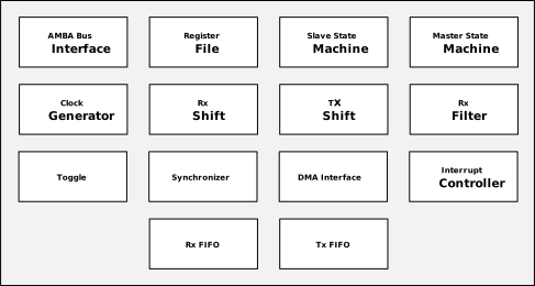
I2C 的功能框图如下图所示。下文定义了各模块的名称和功能:
AMBA 总线接口:接收来自片上 APB 总线的访问信号,并将其映射到内部通用寄存器接口,使寄存器堆与总线协议解耦,增强模块的可移植性。
寄存器堆:包含所有软件可访问的配置寄存器和状态寄存器,是处理器控制 I2C 硬件的核心接口,用于完成参数配置、数据收发命令写入、中断使能及状态查询等操作。
从机状态机:持续监听总线上的 START 条件,将接收到的 7 位或 10 位地址与 IC_SAR 寄存器中的本机地址比对,匹配成功后自动回应 ACK 并完成数据收发;支持广播呼叫地址的识别。
主机状态机:根据软件写入 IC_DATA_CMD 寄存器的命令,自动依次生成 START 条件、地址帧、数据帧及 STOP/RESTART 条件,并管理 ACK/NACK 的接收判断;在多主机场景下自动参与总线仲裁,仲裁失败时触发仲裁丢失中断并退出传输。
时钟发生器:根据 IC_SS_SCL_HCNT/LCNT、IC_FS_SCL_HCNT/LCNT 等寄存器配置,产生符合 I2C 规范的 SCL 时序,具体职责包括:
配置为主机时,生成 SCL 时钟
检查总线是否空闲
生成起始和停止信号
控制数据建立时间和数据保持时间,确保 SDA 在 SCL 边沿前后的电平稳定时窗满足规范要求
Rx 移位器:以 MSB 优先顺序串行接收 SDA 线上的数据,每凑满 8 位推送一个完整字节至 Rx FIFO,并在每字节末自动驱动 ACK 或 NACK 位到 SDA。
Tx 移位器:从 Tx FIFO 取出待发送字节,以 MSB 优先顺序逐位驱动 SDA 线;若采样到 NACK,则触发 TX_ABRT 中断,中止传输并强制清空 Tx FIFO。
Rx 滤波器:对输入的 SDA 和 SCL 信号进行数字去毛刺滤波,抑制总线噪声,并准确检测 START 条件、STOP 条件及仲裁丢失等关键总线事件,为主/从机状态机提供可靠的触发源。
Toggle:将源时钟域产生的单次脉冲转换为电平翻转信号,由目标侧的同步器检测翻转后还原为脉冲,实现跨异步时钟域的单次事件通知。
同步器:采用两级触发器结构对跨异步时钟域的电平信号进行同步化处理,消除亚稳态风险;与 Toggle 模块配合使用,共同完成电平信号和单次脉冲事件的安全跨域传输。
DMA 接口:根据 Tx FIFO 和 Rx FIFO 的数据量,适时向 DMAC 发出请求信号,由 DMAC 自动完成内存与 I2C FIFO 之间的数据搬运,无需 CPU 介入;适合主机模式下长报文数据的高效传输。
中断控制器:汇总各内部事件产生的原始中断,经 IC_INTR_MASK 寄存器屏蔽后生成中断请求;支持通过读取 IC_RAW_INTR_STAT 查询原始事件状态,并通过 IC_CLR_* 寄存器单独清除各中断标志。常见中断源包括:RX_FULL、TX_EMPTY、TX_ABRT、RD_REQ、STOP_DET 等。
Rx FIFO / Tx FIFO:包含相互独立的接收 FIFO 和发送 FIFO,各自配备读写指针及满/空状态控制器。Rx FIFO 缓存从总线接收的数据直至软件读取,Tx FIFO 缓存待发送数据供移位器逐字节取用;可分别通过 IC_RX_TL 和 IC_TX_TL 寄存器配置中断触发阈值。
功能描述
互联拓扑
I2C 总线是一种双线串行接口,由一根串行数据线 (SDA) 和一根串行时钟线 (SCL) 组成。这两条信号线在连接到总线的设备之间传输信息。数据以字节包的形式传输。
SCL 和 SDA 引脚上的输出驱动器为开漏 (Open-drain) 或集电极开路 (Open-collector) 结构,需外接上拉电阻。这使得总线上能够执行线与 (Wire-AND) 功能。总线上的最大设备数量仅受 400pF 的最大电容规格限制。
每个设备通过一个唯一的地址来识别,并且可以根据设备的功能作为 "发送器" 或 "接收器" 工作。
在执行数据传输时,设备可被划分为主机或从机。主机是发起总线上的数据传输并产生时钟信号以控制该传输的设备。此时,任何被寻址的设备都被视为从机。
备注
I2C 必须配置为仅在主机模式或仅在从机模式下工作。不支持同时作为主机和从机运行。
任何 I2C 设备都可以连接到 I2C 总线,每个设备都可以与任一主机通信,实现信息的双向传递。
总线上至少需要有一个主机(如微控制器或 DSP),允许存在多个主机。当存在多个主机时,它们需要通过仲裁 (Arbitration) 来竞争总线的控制权。关于多主机和仲裁机制,将在本节后续部分详细说明。
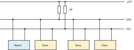
下图展示了一个主机和三个从机节点的连接示例:
I2C 通信协议
本节介绍 I2C 协议基础,包括以下内容:
I2C 设备角色定义
START 和 STOP 条件
寻址模式
数据传输协议
I2C 设备角色定义
主机 —— 负责初始化传输(START 命令)、生成时钟 (SCL) 信号并终止传输(STOP 命令)。主机可以是发送器或接收器。
从机 —— 被主机寻址的设备。从机既可以是接收器,也可以是发送器。
发送器 —— 向总线发送数据的设备。发送器既可以是发起数据传输的设备(主机发送器,Master-Transmitter),也可以是响应主机请求向总线发送数据的设备(从机发送器,Slave-Transmitter)。
接收器 —— 从总线接收数据的设备。接收器既可以是发起接收数据的设备(主机接收器,Master-Receiver),也可以是响应主机请求接收数据的设备(从机接收器,Slave-Receiver)。
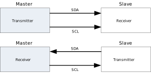
下图展示了主机、从机以及发送器和接收器之间的关系:
I2C 支持多主机功能,即允许多个主机同时存在于总线上,而不会发生冲突或数据丢失。此功能涉及以下硬件机制:
仲裁 —— 用于决定总线所有权,确保一次只有一个主机控制总线。
同步 —— 用于同步多个主机提供的时钟信号。
START 和 STOP 条件
START 和 STOP 条件的定义如下:
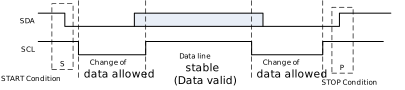
START/RESTART —— 数据传输以 START 或 RESTART 条件开始。当 SCL 时钟线保持高电平时,SDA 数据线的电平从高变为低。当这种信号产生时,总线变为忙状态。
STOP —— 数据传输由 STOP 条件终止。当 SCL 时钟线保持高电平时,SDA 数据线的电平从低变为高。当数据传输终止后,总线恢复空闲状态。如果生成的是 RESTART 而不是 STOP 条件,则总线保持忙状态。
备注
START 和 RESTART 条件在功能上是相同的。
当总线空闲时,SCL 和 SDA 信号都通过总线上的外部上拉电阻被拉高。
当主机想要在总线上启动传输时,主机发出 START 条件。定义为:当 SCL 为高电平时,SDA 信号从高变低。
当主机想要终止传输时,主机发出 STOP 条件。定义为:当 SCL 为高电平时,SDA 信号从低变高。
下图显示了 START 和 STOP 条件的时序。当数据在总线上传输时,当 SCL 为高电平时,SDA 线必须保持稳定。
寻址模式
I2C 支持两种地址格式:7 位和 10 位。
7 位地址格式
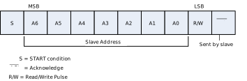
在 7 位地址格式中,第一个字节的前七位(bit[7:1])设置从机地址,最低位 LSB(bit[0])是 R/W (读/写) 位,如下图所示。当 bit[0] 设置为 0 时,主机向从机写入数据。当 bit[0] 设置为 1 时,主机从从机读取数据。
10 位地址格式
在 10 位寻址期间,传输两个字节以设置 10 位地址:
第一个字节:前五位(bit[7:3])固定为 5'b11110,通知从机这是 10 位地址传输;随后两位(bit[2:1])是从机地址的高 2 位(bit[9:8]),最低位 LSB(bit[0])是 R/W 位。
第二个字节:从机地址的低 8 位(bit[7:0])。
下图显示了 10 位地址格式,表格中 定义了特殊用途和保留的第一字节地址。

从机地址 |
R/W 位 |
描述 |
|---|---|---|
0000 000 |
0 |
通用呼叫地址。I2C 将数据放入接收缓冲区,并发出通用呼叫中断。 |
0000 000 |
1 |
START 字节 |
0000 001 |
x |
CBUS 地址。I2C 忽略这些访问。 |
0000 010 |
x |
保留 |
0000 011 |
x |
保留 |
0000 1XX |
x |
高速主机代码 |
1111 1XX |
x |
保留 |
1111 0XX |
x |
10 位从机寻址 |
I2C 不限制使用这些保留地址。但是,如果使用了保留地址,可能会遇到与其他 I2C 组件不兼容的问题。
数据传输协议
I2C 可以通过软件配置为以下任一模式:
仅作为 I2C 主机,与其他 I2C 从机通信;
仅作为 I2C 从机,与一个或多个 I2C 主机通信。
主机负责产生时钟并控制数据传输。从机负责向主机发送或接收来自主机的数据。数据的应答 (ACK) 由接收数据的设备发送,该设备可以是主机或从机。
每个从机都有一个唯一的地址,该地址由系统设计者确定。当主机想要与从机通信时,主机首先发送 START/RESTART 条件,然后发送从机地址和一个控制位(R/W),R/W 位表示主机想要发送数据还是接收数据。随后,该地址对应的从机将发送一个 ACK 脉冲。
主机可以启动写数据或读数据传输,分别作为主机发送器或主机接收器。从机响应主机的请求,向总线发送或从总线接收数据,分别作为从机发送器或从机接收器:
主机写:从机作为接收器,以字节为单位接收数据,持续传输,直到主机通过 STOP 条件终止传输。
主机读:从机向主机发送一个字节的数据,主机随即发送 ACK 脉冲进行应答。此过程持续进行,直到主机在收到最后一个字节后不发送应答(NACK)来终止传输,随后主机发出 STOP 条件,或者发出 RESTART 条件以寻址另一个从机。
此行为如下图所示:
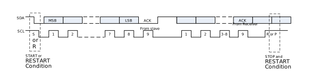
I2C 是一种同步串行接口。SDA 线是双向信号。在数据传输过程中,SDA 线上的信号必须在 SCL 为高电平期间保持稳定;只有在 SCL 线为低电平期间发生改变,除了 STOP、START 和 RESTART 条件。
START 字节传输协议
微控制器可以通过两种方式连接到 I2C 总线:
通过 START 字节请求中断:具有片上硬件 I2C 总线接口的微控制器可以被编程为仅被总线的请求中断。
轮询总线:当设备没有此类接口时,它必须不断监听总线。显然,微控制器轮询总线的次数越多,执行其预定功能的时间就越少。由此,快速外设和微控制器之间将产生速度差异,因为后者依赖软件轮询,相对较慢。
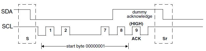
如上图所示,START 字节过程如下:
主机生成 START 条件。
主机发送 START 字节 (0000 0001)。
主机发送 ACK 时钟(SCL)脉冲。(存在仅为了符合总线的字节处理格式)
没有从机会响应 START 字节,SDA 线不会被拉低。
主机生成 RESTART (Sr) 条件。
在需要总线访问的主机传输 START 条件 S 后,传输 START 字节 (0000 0001)。因此,另一个微控制器可以以低采样率对 SDA 线进行采样,直到检测到 START 字节中的七个零之一。在检测到 SDA 线上的低电平后,微控制器可以切换到更高的采样率以找到 RESTART 条件(Sr),该条件随后用于同步。
硬件接收器将在接收到 Sr 条件时复位,因此将忽略 START 字节。
在 START 字节之后生成一个与应答相关的时钟脉冲。它的存在仅仅是为了符合总线上使用的字节处理格式。不允许任何设备应答 START 字节。
硬件接收器不响应 START 字节,因为它是保留地址,并且在生成 RESTART 条件后复位。
广播呼叫传输协议
广播呼叫 (General Call) 用于主机向连接到 I2C 总线的所有设备发送相同的指令或数据。
当主机发出广播地址(首字节为 0x00,且 R/W 位为 0)时,如果从机不需要处理广播信息,直接忽略(不回复 ACK)即可;如果从机支持并需要该指令,则回复 ACK 并开始接收后面的数据字节。
下图给出了广播呼叫地址格式。第二个字节可以是:
'h06:通知总线上的从机执行硬件复位,并重新载入它们的可编程地址。
'h04:通知从机更新其可编程地址(不执行复位)。
发送主机自己的 7 位地址,用于向从机广播主机地址。

当 I2C 作为从机时,若需响应主机的广播呼叫,用户需配置 IC_ACK_GENERAL_CALL (0x98) bit[0] 为 1。使能后,I2C 收到广播地址时会自动回复 ACK,并产生一个广播中断通知软件处理。若置为 0,则直接无视总线上的所有广播信号。
空数据传输协议
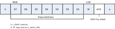
空数据(NULL DATA)传输用于某些传感器。只需要接收到主机的 START 条件和从机地址,传感器就会触发状态切换、开始测量等操作,而不需要附加任何数据。
在常规发送模式中,目标从机地址是由 IC_TAR 寄存器配置,而 TXFIFO 用于存放数据。当 IC_DATA_CMD [11] 和 IC_DATA_CMD [9] 同时设置为 1 时,I2C 将忽略 IC_TAR 寄存器,而是将 TXFIFO 中的数据作为从机地址,在地址阶段发送到总线,随后发出 STOP 条件终止通信,不会有任何后续数据被发送。
下图给出了空数据传输格式:
主机模式
本节介绍 I2C 主机模式的协议和操作流程。I2C 主机模式是指 I2C 设备作为主机运行,控制总线并与一个或多个从机通信。在主机模式下,I2C 负责生成时钟,生成 START 和 STOP 条件,并根据协议发送和接收数据。
START 和 STOP 的生成
请参考 寄存器结构 了解 IC_DATA_CMD 结构。
当作为 I2C 主机运行时:
将数据放入发送 FIFO 会导致 I2C 在总线上生成 START 条件。
向 IC_DATA_CMD [9] 写入 1 会导致硬件在 I2C 总线上生成 STOP 条件;如果未将此位置位,即使发送 FIFO 为空,也不会发出 STOP 条件。
向 IC_DATA_CMD [10] 写入 1 会导致硬件在当前数据传输完成后保持对总线的占用,并在 FIFO 中的下一个数据准备好在总线上传输时生成 RESTART 条件。
当作为从机运行时,根据协议,I2C 不会生成 START 和 STOP 条件。但是,如果向该 I2C 发出了读请求,它将保持 SCL 线为低电平,直到向其提供数据。这将阻塞 I2C 总线,直到待读取数据被提供给从机 I2C,或者通过向 IC_ENABLE 寄存器的 bit0 写入 0 来禁用 I2C 从机。
速度与时钟配置
I2C 接口的总线时钟频率和速度模式如下:
2 个 I2C 接口,I2C0 和 I2C1 的总线时钟为 40MHz,支持所有速度模式。
2 个 I2C 接口,I2C0 和 I2C1 的总线时钟为 100MHz,支持所有速度模式。
2 个 I2C 接口,I2C0 和 I2C1 的总线时钟为 100MHz,支持所有速度模式。
2 个 I2C 接口,I2C0 和 I2C1 的总线时钟为 100MHz,支持所有速度模式。
2 个 I2C 接口,I2C0 和 I2C1 的总线时钟为 100MHz,支持所有速度模式。
3 个 I2C 接口:
I2C0 的总线时钟为 20MHz,仅支持标准模式和快速模式。
I2C1 和 I2C2 的总线时钟为 100MHz,支持所有速度模式。
2 个 I2C 接口,I2C0 和 I2C1 的总线时钟为 40MHz,支持所有速度模式。
2 个 I2C 接口,I2C0 和 I2C1 的总线时钟为 100MHz,支持所有速度模式。
当 I2C 配置为主机时,在开始 I2C 传输之前,必须设置 *CNT 寄存器,以确保正确的 I/O 时序。*CNT 寄存器包括:
IC_SS_SCL_HCNT
IC_SS_SCL_LCNT
IC_FS_SCL_HCNT
IC_FS_SCL_LCNT
IC_HS_SCL_HCNT
IC_HS_SCL_LCNT
其中, SS、 FS 和 HS 分别代表标准模式、快速模式和高速模式。*HCNT 寄存器用于设置 SCL 高电平持续的时钟周期数,*LCNT 寄存器用于设置 SCL 低电平持续的时钟周期数。
备注
如果 I2C 配置为从机,则不需要设置任何 *CNT 寄存器,因为这些寄存器仅用于确定作为 I2C 主机时的 SCL 时序要求。
高电平和低电平周期数计算
下面展示了如何计算 I2C 每种速度模式的 SCL 高电平和低电平周期数。
应提供以下条件:
ic_clk 频率:fic_clk → Tic_clk = 1 / fic_clk
HIGH_TIME:SCL 的高电平时长
LOW_TIME:SCL 的低电平时长
SCL 频率:fSCL → SCLPERIOD = 1 / fSCL
要求取 HIGH_COUNT 和 LOW_COUNT ,我们可以进行以下推导:
SCL_PERIOD / (HIGH_COUNT + LOW_COUNT) = T_ic_clk
HIGH_COUNT / HIGH_TIME = LOW_COUNT / LOW_TIME
HIGH_TIME + LOW_TIME = SCL_PERIOD
然后可以得到:
HIGH_COUNT = HIGH_TIME / T_ic_clk
LOW_COUNT = LOW_TIME / T_ic_clk
标准速度模式和快速模式示例
对于 I2C0/I2C1,fic_clk = 40MHz
ic_clk 频率:fic_clk = 40MHz → Tic_clk = 25ns
根据 I2C-Bus specification version2.1 的表 5,FS 模式和 SS 模式的 SCL 时序参数规定如下:
标准模式:SCL 最小高电平时间为 4.0us(最小 IC_SS_SCL_HCNT = 4.0us/25ns = 160)
标准模式:SCL 最小低电平时间为 4.7us(最小 IC_SS_SCL_LCNT = 4.7us/25ns = 188)
快速模式:SCL 最小高电平时间为 0.6us(最小 IC_FS_SCL_HCNT = 0.6us/25ns = 24)
快速模式:SCL 最小低电平时间为 1.3us(最小 IC_FS_SCL_LCNT = 1.3us/25ns = 52)
SCL 频率:
100kHz → SCLPERIOD = 10000ns
400kHz → SCLPERIOD = 2500ns
SS 模式 (100kHz):
IC_SS_SCL_HCNT = (10000ns/25ns)*(40/(40+47)) = 183.91 = 184(向上取整)
IC_SS_SCL_LCNT = (10000ns/25ns)*(47/(40+47)) = 216.09 = 216(向下取整)
FS 模式 (400kHz):
IC_FS_SCL_HCNT = (2500ns/25ns)*(6/(6+13)) = 31.58 = 32(向上取整)
IC_FS_SCL_LCNT = (2500ns/25ns)*(13/(6+13)) = 68.42 = 68(向下取整)
对于 I2C0/I2C1,fic_clk = 100MHz
ic_clk 频率:fic_clk = 100MHz → Tic_clk = 10ns
根据 I2C-Bus specification version2.1 的表 5,FS 模式和 SS 模式的 SCL 时序参数规定如下:
标准模式:SCL 最小高电平时间为 4.0us(最小 IC_SS_SCL_HCNT = 4.0us/10ns = 400)
标准模式:SCL 最小低电平时间为 4.7us(最小 IC_SS_SCL_LCNT = 4.7us/10ns = 470)
快速模式:SCL 最小高电平时间为 0.6us(最小 IC_FS_SCL_HCNT = 0.6us/10ns = 60)
快速模式:SCL 最小低电平时间为 1.3us(最小 IC_FS_SCL_LCNT = 1.3us/10ns = 130)
SCL 频率:
100kHz → SCLPERIOD = 10000ns
400kHz → SCLPERIOD = 2500ns
SS 模式(100kHz):
IC_SS_SCL_HCNT = (10000ns/10ns)*(40/(40+47)) = 459.77 = 460(向上取整)
IC_SS_SCL_LCNT = (10000ns/10ns)*(47/(40+47)) = 540.23 = 540(向下取整)
FS 模式(400kHz):
IC_FS_SCL_HCNT = (2500ns/10ns)*(6/(6+13)) = 78.95 = 79(向上取整)
IC_FS_SCL_LCNT = (2500ns/10ns)*(13/(6+13)) = 171.05 = 171(向下取整)
对于 I2C0/I2C1,fic_clk = 100MHz
ic_clk 频率:fic_clk = 100MHz → Tic_clk = 10ns
根据 I2C-Bus specification version2.1 的表 5,FS 模式和 SS 模式的 SCL 时序参数规定如下:
标准模式:SCL 最小高电平时间为 4.0us(最小 IC_SS_SCL_HCNT = 4.0us/10ns = 400)
标准模式:SCL 最小低电平时间为 4.7us(最小 IC_SS_SCL_LCNT = 4.7us/10ns = 470)
快速模式:SCL 最小高电平时间为 0.6us(最小 IC_FS_SCL_HCNT = 0.6us/10ns = 60)
快速模式:SCL 最小低电平时间为 1.3us(最小 IC_FS_SCL_LCNT = 1.3us/10ns = 130)
SCL 频率:
100kHz → SCLPERIOD = 10000ns
400kHz → SCLPERIOD = 2500ns
SS 模式(100kHz):
IC_SS_SCL_HCNT = (10000ns/10ns)*(40/(40+47)) = 459.77 = 460(向上取整)
IC_SS_SCL_LCNT = (10000ns/10ns)*(47/(40+47)) = 540.23 = 540(向下取整)
FS 模式(400kHz):
IC_FS_SCL_HCNT = (2500ns/10ns)*(6/(6+13)) = 78.95 = 79(向上取整)
IC_FS_SCL_LCNT = (2500ns/10ns)*(13/(6+13)) = 171.05 = 171(向下取整)
对于 I2C0/I2C1,fic_clk = 100MHz
ic_clk 频率:fic_clk = 100MHz → Tic_clk = 10ns
根据 I2C-Bus specification version2.1 的表 5,FS 模式和 SS 模式的 SCL 时序参数规定如下:
标准模式:SCL 最小高电平时间为 4.0us(最小 IC_SS_SCL_HCNT = 4.0us/10ns = 400)
标准模式:SCL 最小低电平时间为 4.7us(最小 IC_SS_SCL_LCNT = 4.7us/10ns = 470)
快速模式:SCL 最小高电平时间为 0.6us(最小 IC_FS_SCL_HCNT = 0.6us/10ns = 60)
快速模式:SCL 最小低电平时间为 1.3us(最小 IC_FS_SCL_LCNT = 1.3us/10ns = 130)
SCL 频率:
100kHz → SCLPERIOD = 10000ns
400kHz → SCLPERIOD = 2500ns
SS 模式(100kHz):
IC_SS_SCL_HCNT = (10000ns/10ns)*(40/(40+47)) = 459.77 = 460(向上取整)
IC_SS_SCL_LCNT = (10000ns/10ns)*(47/(40+47)) = 540.23 = 540(向下取整)
FS 模式(400kHz):
IC_FS_SCL_HCNT = (2500ns/10ns)*(6/(6+13)) = 78.95 = 79(向上取整)
IC_FS_SCL_LCNT = (2500ns/10ns)*(13/(6+13)) = 171.05 = 171(向下取整)
对于 I2C0/I2C1,fic_clk = 100MHz
ic_clk 频率:fic_clk = 100MHz → Tic_clk = 10ns
根据 I2C-Bus specification version2.1 的表 5,FS 模式和 SS 模式的 SCL 时序参数规定如下:
标准模式:SCL 最小高电平时间为 4.0us(最小 IC_SS_SCL_HCNT = 4.0us/10ns = 400)
标准模式:SCL 最小低电平时间为 4.7us(最小 IC_SS_SCL_LCNT = 4.7us/10ns = 470)
快速模式:SCL 最小高电平时间为 0.6us(最小 IC_FS_SCL_HCNT = 0.6us/10ns = 60)
快速模式:SCL 最小低电平时间为 1.3us(最小 IC_FS_SCL_LCNT = 1.3us/10ns = 130)
SCL 频率:
100kHz → SCLPERIOD = 10000ns
400kHz → SCLPERIOD = 2500ns
SS 模式(100kHz):
IC_SS_SCL_HCNT = (10000ns/10ns)*(40/(40+47)) = 459.77 = 460(向上取整)
IC_SS_SCL_LCNT = (10000ns/10ns)*(47/(40+47)) = 540.23 = 540(向下取整)
FS 模式(400kHz):
IC_FS_SCL_HCNT = (2500ns/10ns)*(6/(6+13)) = 78.95 = 79(向上取整)
IC_FS_SCL_LCNT = (2500ns/10ns)*(13/(6+13)) = 171.05 = 171(向下取整)
对于 I2C0,fic_clk = 20MHz;对于 I2C1/I2C2,fic_clk = 100MHz
ic_clk 频率:fic_clk = 20MHz → Tic_clk = 50ns
根据 I2C-Bus 规范 version2.1 的表 5,SCL 的 FS 模式和 SS 模式时序参数规定如下:
标准模式:SCL 最小高电平时间为 4.0us(最小 IC_SS_SCL_HCNT = 4.0us/50ns = 80)
标准模式:SCL 最小低电平时间为 4.7us(最小 IC_SS_SCL_LCNT = 4.7us/50ns = 94)
快速模式:SCL 最小高电平时间为 0.6us(最小 IC_FS_SCL_HCNT = 0.6us/50ns = 12)
快速模式:SCL 最小低电平时间为 1.3us(最小 IC_FS_SCL_LCNT = 1.3us/50ns = 26)
SCL 频率:
100kHz → SCLPERIOD = 10000ns
400kHz → SCLPERIOD = 2500ns
SS 模式 (100kHz):
IC_SS_SCL_HCNT = (10000ns/50ns)*(40/(40+47)) = 91.95 = 92 (向上取整)
IC_SS_SCL_LCNT = (10000ns/50ns)*(47/(40+47)) = 108.05 = 108 (向下取整)
FS 模式 (400kHz):
IC_FS_SCL_HCNT = (2500ns/50ns)*(6/(6+13)) = 15.79 = 16 (向上取整)
IC_FS_SCL_LCNT = (2500ns/50ns)*(13/(6+13)) = 34.21 = 34 (向下取整)
对于 I2C0/I2C1,fic_clk = 40MHz
ic_clk 频率:fic_clk = 40MHz → Tic_clk = 25ns
根据 I2C-Bus specification version2.1 的表 5,FS 模式和 SS 模式的 SCL 时序参数规定如下:
标准模式:SCL 最小高电平时间为 4.0us(最小 IC_SS_SCL_HCNT = 4.0us/25ns = 160)
标准模式:SCL 最小低电平时间为 4.7us(最小 IC_SS_SCL_LCNT = 4.7us/25ns = 188)
快速模式:SCL 最小高电平时间为 0.6us(最小 IC_FS_SCL_HCNT = 0.6us/25ns = 24)
快速模式:SCL 最小低电平时间为 1.3us(最小 IC_FS_SCL_LCNT = 1.3us/25ns = 52)
SCL 频率:
100kHz → SCLPERIOD = 10000ns
400kHz → SCLPERIOD = 2500ns
SS 模式 (100kHz):
IC_SS_SCL_HCNT = (10000ns/25ns)*(40/(40+47)) = 183.91 = 184(向上取整)
IC_SS_SCL_LCNT = (10000ns/25ns)*(47/(40+47)) = 216.09 = 216(向下取整)
FS 模式 (400kHz):
IC_FS_SCL_HCNT = (2500ns/25ns)*(6/(6+13)) = 31.58 = 32(向上取整)
IC_FS_SCL_LCNT = (2500ns/25ns)*(13/(6+13)) = 68.42 = 68(向下取整)
对于 I2C0/I2C1,fic_clk = 100MHz
ic_clk 频率:fic_clk = 100MHz → Tic_clk = 10ns
根据 I2C-Bus specification version2.1 的表 5,FS 模式和 SS 模式的 SCL 时序参数规定如下:
标准模式:SCL 最小高电平时间为 4.0us(最小 IC_SS_SCL_HCNT = 4.0us/10ns = 400)
标准模式:SCL 最小低电平时间为 4.7us(最小 IC_SS_SCL_LCNT = 4.7us/10ns = 470)
快速模式:SCL 最小高电平时间为 0.6us(最小 IC_FS_SCL_HCNT = 0.6us/10ns = 60)
快速模式:SCL 最小低电平时间为 1.3us(最小 IC_FS_SCL_LCNT = 1.3us/10ns = 130)
SCL 频率:
100kHz → SCLPERIOD = 10000ns
400kHz → SCLPERIOD = 2500ns
SS 模式(100kHz):
IC_SS_SCL_HCNT = (10000ns/10ns)*(40/(40+47)) = 459.77 = 460(向上取整)
IC_SS_SCL_LCNT = (10000ns/10ns)*(47/(40+47)) = 540.23 = 540(向下取整)
FS 模式(400kHz):
IC_FS_SCL_HCNT = (2500ns/10ns)*(6/(6+13)) = 78.95 = 79(向上取整)
IC_FS_SCL_LCNT = (2500ns/10ns)*(13/(6+13)) = 171.05 = 171(向下取整)
高速模式示例
I2C0 和 I2C1 都支持 HS 模式,fic_clk = 40MHz
ic_clk 频率:fic_clk = 40MHz → Tic_clk = 25ns
根据 I2C 总线规范版本 2.1 的表 7,HS 模式 SCL 的时序参数指定为:
3.4MHz,总线负载=100pf:SCL 的最小高电平期间为 60ns(最小 IC_HS_SCL_HCNT = 60ns/25ns = 2.4 → 3)
3.4MHz,总线负载=100pf:SCL 的最小低电平期间为 120ns(最小 IC_HS_SCL_LCNT = 120ns/25ns = 4.8 → 5)
1.7MHz,总线负载=400pf:SCL 的最小高电平期间为 160ns(最小 IC_HS_SCL_HCNT = 160ns/25ns = 6.4 → 7)
1.7MHz,总线负载=400pf:SCL 的最小低电平期间为 320ns(最小 IC_HS_SCL_LCNT = 320ns/25ns = 12.8 → 13)
SCL 频率:
3.4MHz → SCLPERIOD = 294ns
1.7MHz → SCLPERIOD = 588ns
HS 模式 (3.4MHz,总线负载=100pf):
IC_HS_SCL_HCNT = (294ns/25ns)*(6/(6+12)) = 3.9 = 4(向上取整)
IC_HS_SCL_LCNT = (294ns/25ns)*(12/(6+12)) = 7.8 = 8(向上取整)
HS 模式 (1.7MHz,总线负载=400pf):
IC_HS_SCL_HCNT = (588ns/25ns)*(16/(16+32)) = 7.8 = 8(向上取整)
IC_HS_SCL_LCNT = (588ns/25ns)*(32/(16+32)) = 15.7 = 16(向上取整)
I2C0 和 I2C1 都支持 HS 模式,fic_clk = 100MHz
ic_clk 频率:fic_clk = 100MHz → Tic_clk = 10ns
根据 I2C 总线规范版本 2.1 的表 7,HS 模式 SCL 的时序参数指定为:
3.4MHz,总线负载=100pf:SCL 的最小高电平期间为 60ns(最小 IC_HS_SCL_HCNT = 60ns/10ns= 6)
3.4MHz,总线负载=100pf:SCL 的最小低电平期间为 120ns(最小 IC_HS_SCL_LCNT = 120ns/10ns= 12)
1.7MHz,总线负载=400pf:SCL 的最小高电平期间为 160ns(最小 IC_HS_SCL_HCNT = 160ns/10ns= 16)
1.7MHz,总线负载=400pf:SCL 的最小低电平期间为 320ns(最小 IC_HS_SCL_LCNT = 320ns/10ns= 32)
SCL 频率:
3.4MHz → SCLPERIOD = 294ns
1.7MHz → SCLPERIOD = 588ns
HS 模式 (3.4MHz,总线负载=100pf):
IC_HS_SCL_HCNT = (294ns/10ns)*(6/(6+12)) = 9.8 = 10(向上取整)
IC_HS_SCL_LCNT = (294ns/10ns)*(12/(6+12)) = 19.6 = 20(向上取整)
HS 模式 (1.7MHz,总线负载=400pf):
IC_HS_SCL_HCNT = (588ns/10ns)*(16/(16+32)) = 19.6 = 20(向上取整)
IC_HS_SCL_LCNT = (588ns/10ns)*(32/(16+32)) = 39.2 = 39(向下取整)
I2C0 和 I2C1 都支持 HS 模式,fic_clk = 100MHz
ic_clk 频率:fic_clk = 100MHz → Tic_clk = 10ns
根据 I2C 总线规范版本 2.1 的表 7,HS 模式 SCL 的时序参数指定为:
3.4MHz,总线负载=100pf:SCL 的最小高电平期间为 60ns(最小 IC_HS_SCL_HCNT = 60ns/10ns= 6)
3.4MHz,总线负载=100pf:SCL 的最小低电平期间为 120ns(最小 IC_HS_SCL_LCNT = 120ns/10ns= 12)
1.7MHz,总线负载=400pf:SCL 的最小高电平期间为 160ns(最小 IC_HS_SCL_HCNT = 160ns/10ns= 16)
1.7MHz,总线负载=400pf:SCL 的最小低电平期间为 320ns(最小 IC_HS_SCL_LCNT = 320ns/10ns= 32)
SCL 频率:
3.4MHz → SCLPERIOD = 294ns
1.7MHz → SCLPERIOD = 588ns
HS 模式 (3.4MHz,总线负载=100pf):
IC_HS_SCL_HCNT = (294ns/10ns)*(6/(6+12)) = 9.8 = 10(向上取整)
IC_HS_SCL_LCNT = (294ns/10ns)*(12/(6+12)) = 19.6 = 20(向上取整)
HS 模式 (1.7MHz,总线负载=400pf):
IC_HS_SCL_HCNT = (588ns/10ns)*(16/(16+32)) = 19.6 = 20(向上取整)
IC_HS_SCL_LCNT = (588ns/10ns)*(32/(16+32)) = 39.2 = 39(向下取整)
I2C0 和 I2C1 都支持 HS 模式,fic_clk = 100MHz
ic_clk 频率:fic_clk = 100MHz → Tic_clk = 10ns
根据 I2C 总线规范版本 2.1 的表 7,HS 模式 SCL 的时序参数指定为:
3.4MHz,总线负载=100pf:SCL 的最小高电平期间为 60ns(最小 IC_HS_SCL_HCNT = 60ns/10ns= 6)
3.4MHz,总线负载=100pf:SCL 的最小低电平期间为 120ns(最小 IC_HS_SCL_LCNT = 120ns/10ns= 12)
1.7MHz,总线负载=400pf:SCL 的最小高电平期间为 160ns(最小 IC_HS_SCL_HCNT = 160ns/10ns= 16)
1.7MHz,总线负载=400pf:SCL 的最小低电平期间为 320ns(最小 IC_HS_SCL_LCNT = 320ns/10ns= 32)
SCL 频率:
3.4MHz → SCLPERIOD = 294ns
1.7MHz → SCLPERIOD = 588ns
HS 模式 (3.4MHz,总线负载=100pf):
IC_HS_SCL_HCNT = (294ns/10ns)*(6/(6+12)) = 9.8 = 10(向上取整)
IC_HS_SCL_LCNT = (294ns/10ns)*(12/(6+12)) = 19.6 = 20(向上取整)
HS 模式 (1.7MHz,总线负载=400pf):
IC_HS_SCL_HCNT = (588ns/10ns)*(16/(16+32)) = 19.6 = 20(向上取整)
IC_HS_SCL_LCNT = (588ns/10ns)*(32/(16+32)) = 39.2 = 39(向下取整)
I2C0 和 I2C1 都支持 HS 模式,fic_clk = 100MHz
ic_clk 频率:fic_clk = 100MHz → Tic_clk = 10ns
根据 I2C 总线规范版本 2.1 的表 7,HS 模式 SCL 的时序参数指定为:
3.4MHz,总线负载=100pf:SCL 的最小高电平期间为 60ns(最小 IC_HS_SCL_HCNT = 60ns/10ns= 6)
3.4MHz,总线负载=100pf:SCL 的最小低电平期间为 120ns(最小 IC_HS_SCL_LCNT = 120ns/10ns= 12)
1.7MHz,总线负载=400pf:SCL 的最小高电平期间为 160ns(最小 IC_HS_SCL_HCNT = 160ns/10ns= 16)
1.7MHz,总线负载=400pf:SCL 的最小低电平期间为 320ns(最小 IC_HS_SCL_LCNT = 320ns/10ns= 32)
SCL 频率:
3.4MHz → SCLPERIOD = 294ns
1.7MHz → SCLPERIOD = 588ns
HS 模式 (3.4MHz,总线负载=100pf):
IC_HS_SCL_HCNT = (294ns/10ns)*(6/(6+12)) = 9.8 = 10(向上取整)
IC_HS_SCL_LCNT = (294ns/10ns)*(12/(6+12)) = 19.6 = 20(向上取整)
HS 模式 (1.7MHz,总线负载=400pf):
IC_HS_SCL_HCNT = (588ns/10ns)*(16/(16+32)) = 19.6 = 20(向上取整)
IC_HS_SCL_LCNT = (588ns/10ns)*(32/(16+32)) = 39.2 = 39(向下取整)
I2C0 不支持 HS 模式;对于 I2C1/2,fic_clk = 100MHz,支持 HS 模式。
ic_clk 频率:fic_clk = 100MHz → Tic_clk = 10ns
根据 I2C 总线规范版本 2.1 的表 7,HS 模式 SCL 的时序参数指定为:
3.4MHz,总线负载=100pf:SCL 的最小高电平期间为 60ns(最小 IC_HS_SCL_HCNT = 60ns/10ns= 6)
3.4MHz,总线负载=100pf:SCL 的最小低电平期间为 120ns(最小 IC_HS_SCL_LCNT = 120ns/10ns= 12)
1.7MHz,总线负载=400pf:SCL 的最小高电平期间为 160ns(最小 IC_HS_SCL_HCNT = 160ns/10ns= 16)
1.7MHz,总线负载=400pf:SCL 的最小低电平期间为 320ns(最小 IC_HS_SCL_LCNT = 320ns/10ns= 32)
SCL 频率:
3.4MHz → SCLPERIOD = 294ns
1.7MHz → SCLPERIOD = 588ns
HS 模式 (3.4MHz,总线负载=100pf):
IC_HS_SCL_HCNT = (294ns/10ns)*(6/(6+12)) = 9.8 = 10 (向上取整)
IC_HS_SCL_LCNT = (294ns/10ns)*(12/(6+12)) = 19.6 = 20 (向上取整)
HS 模式 (1.7MHz,总线负载=400pf):
IC_HS_SCL_HCNT = (588ns/10ns)*(16/(16+32)) = 19.6 = 20 (向上取整)
IC_HS_SCL_LCNT = (588ns/10ns)*(32/(16+32)) = 39.2 = 39 (向下取整)
I2C0 和 I2C1 都支持 HS 模式,fic_clk = 40MHz
ic_clk 频率:fic_clk = 40MHz → Tic_clk = 25ns
根据 I2C 总线规范版本 2.1 的表 7,HS 模式 SCL 的时序参数指定为:
3.4MHz,总线负载=100pf:SCL 的最小高电平期间为 60ns(最小 IC_HS_SCL_HCNT = 60ns/25ns = 2.4 → 3)
3.4MHz,总线负载=100pf:SCL 的最小低电平期间为 120ns(最小 IC_HS_SCL_LCNT = 120ns/25ns = 4.8 → 5)
1.7MHz,总线负载=400pf:SCL 的最小高电平期间为 160ns(最小 IC_HS_SCL_HCNT = 160ns/25ns = 6.4 → 7)
1.7MHz,总线负载=400pf:SCL 的最小低电平期间为 320ns(最小 IC_HS_SCL_LCNT = 320ns/25ns = 12.8 → 13)
SCL 频率:
3.4MHz → SCLPERIOD = 294ns
1.7MHz → SCLPERIOD = 588ns
HS 模式 (3.4MHz,总线负载=100pf):
IC_HS_SCL_HCNT = (294ns/25ns)*(6/(6+12)) = 3.9 = 4(向上取整)
IC_HS_SCL_LCNT = (294ns/25ns)*(12/(6+12)) = 7.8 = 8(向上取整)
HS 模式 (1.7MHz,总线负载=400pf):
IC_HS_SCL_HCNT = (588ns/25ns)*(16/(16+32)) = 7.8 = 8(向上取整)
IC_HS_SCL_LCNT = (588ns/25ns)*(32/(16+32)) = 15.7 = 16(向上取整)
I2C0 和 I2C1 都支持 HS 模式,fic_clk = 100MHz
ic_clk 频率:fic_clk = 100MHz → Tic_clk = 10ns
根据 I2C 总线规范版本 2.1 的表 7,HS 模式 SCL 的时序参数指定为:
3.4MHz,总线负载=100pf:SCL 的最小高电平期间为 60ns(最小 IC_HS_SCL_HCNT = 60ns/10ns= 6)
3.4MHz,总线负载=100pf:SCL 的最小低电平期间为 120ns(最小 IC_HS_SCL_LCNT = 120ns/10ns= 12)
1.7MHz,总线负载=400pf:SCL 的最小高电平期间为 160ns(最小 IC_HS_SCL_HCNT = 160ns/10ns= 16)
1.7MHz,总线负载=400pf:SCL 的最小低电平期间为 320ns(最小 IC_HS_SCL_LCNT = 320ns/10ns= 32)
SCL 频率:
3.4MHz → SCLPERIOD = 294ns
1.7MHz → SCLPERIOD = 588ns
HS 模式 (3.4MHz,总线负载=100pf):
IC_HS_SCL_HCNT = (294ns/10ns)*(6/(6+12)) = 9.8 = 10(向上取整)
IC_HS_SCL_LCNT = (294ns/10ns)*(12/(6+12)) = 19.6 = 20(向上取整)
HS 模式 (1.7MHz,总线负载=400pf):
IC_HS_SCL_HCNT = (588ns/10ns)*(16/(16+32)) = 19.6 = 20(向上取整)
IC_HS_SCL_LCNT = (588ns/10ns)*(32/(16+32)) = 39.2 = 39(向下取整)
备注
在实际应用中,由于从机可能触发时钟延展(Clock Stretching)等因素,实际传输速度通常会低于 100kbps/400kbps/3.4Mbps 的目标值。为了达到准确的通信速度,建议根据实际测试结果适当减小计算出的 *CNT 寄存器的值。
主机发送
所有数据均以字节格式传输,每次传输的字节数没有限制。
在主机发送地址和 R/W 位后,或者主机向从机发送一个字节的数据后,从机必须用应答信号 (ACK) 进行响应。
当从机没有用 ACK 脉冲响应时,主机通过发出 STOP 条件中止传输。从机必须保持 SDA 线为高电平,以便主机可以中止传输。
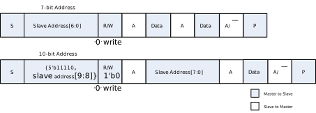
如下图所示,主机发送数据时,从机在每接收一个字节的数据后,都会向主机发送一个应答脉冲。
主机接收
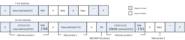
如下图所示,主机接收数据时,每接收到一个字节的数据后,发送应答脉冲响应从机。
最后一个字节接收完成后,主机不发送 ACK,以此来通知从机传输结束。从机在检测到 NACK 后释放 SDA 线,随后主机发出 STOP 条件。
对于 10 位地址,传输过程如下:
地址阶段 1:主机发送 {5'b11110, 从机地址 [9:8], 1'b0};R/W=1'b0 表示主机将发送数据。
数据阶段 1:主机发送从机地址 [7:0]。
发送 RESTART 条件,以切换数据传输方向。
地址阶段 2:主机发送 {5'b11110, 从机地址 [9:8], 1'b1};R/W=1'b1 表示主机将接收数据。
数据阶段 2:主机从从机接收数据。
当主机不想用 STOP 条件释放总线时,可以发出 RESTART 条件。这与 START 条件等效,只是 RESTART 出现在 ACK 脉冲后。在主机模式下运行时,I2C 可以使用不同方向的传输与同一从机进行通信。
复合格式传输
I2C 支持复合格式传输。是指在一次传输过程中,数据发送方向可能改变。例如,主机可能先发送数据然后接收数据,而不释放 I2C 总线,反之亦然。如下图所示:
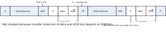
I2C 的复合格式传输支持 7 位或 10 位地址。但不支持混合地址,即在 7 位地址模式的传输后再进行 10 位地址模式的传输,反之亦然。
要启动复合格式传输, IC_CON.IC_RESTART_EN 应设置为 1。此位被置位并作为主机运行时:
当 I2C 完成一次传输时,它会检查发送 FIFO 并执行下一次传输。
如果此传输的方向与前一次传输不同,则使用复合格式来发起传输。
如果当前 I2C 传输完成时发送 FIFO 为空,则检查 IC_DATA_CMD [9]:
如果设置为 1,则发出 STOP 条件。
如果设置为 0,则 SCL 保持为低电平,直到下一个命令写入发送 FIFO。
多主机
I2C 支持多主机功能,允许多个主机在总线上共存而不会发生冲突或数据丢失。
SCL 时钟同步
当两个或多个主机尝试同时在总线上传输信息时,它们必须进行仲裁并同步 SCL 时钟。
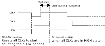
所有主机都生成自己的时钟来传输消息。数据仅在 SCL 时钟的高电平期间有效。时钟同步是利用 SCL 信号的“线与”来实现的。
当某个主机将 SCL 线拉低时,它开始计算自身的低电平时间,准备在低电平时间结束后释放 SCL 以使其变为高电平。然而,由于“线与”逻辑的存在,如果此时另一个主机仍在将 SCL 保持为低电平,那么 SCL 线并不会被拉高;最先结束低电平计数的主机此时将进入“高电平等待状态”,直到总线上所有主机都结束低电平周期,SCL 线真正变为高电平为止。
随后,所有主机开始累计自己的高电平时间,高电平时间最短的主机会将 SCL 线切换为低电平。接着,各主机对各自的低电平时间进行计数,而低电平时间最长的主机会迫使其他主机进入“高电平等待状态”。因此,生成了一个同步的 SCL 时钟,如下图所示。
其中,CLKA 是主机 A 生成的 I2C 总线时钟,CLKB 是主机 B 生成的 I2C 总线时钟。图中的 SCL 是 CLKA 和 CLKB 的线与结果。
SDA 仲裁机制
I2C 总线协议允许多个主机连接在同一总线上。I2C 主机只有在总线空闲时才能启动传输。多个 I2C 主机可能在极短的时间间隔内生成 START 条件来启动传输。
如果两个主机在最小保持时间 (tHD, STA) 内在总线上发送 START,那么当 SCL 线为高电平(1)时,仲裁将在 SDA 线上进行。当一个主机发送高电平(1)而另一个主机发送低电平(0)时,发送高电平(1)的主机将输掉仲裁,并停止输出数据和时钟。
其中,SCL 信号是所有主机的 SCL 信号的线与结果。
下图说明了两个主机在总线上进行仲裁时的时序。
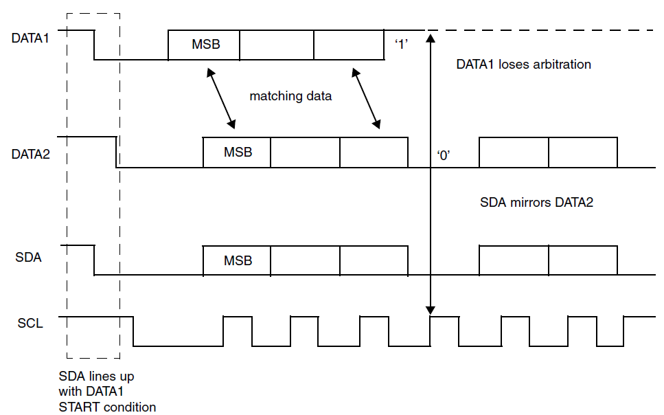
对于 SS 模式或 FS 模式的主机,仲裁可能会持续到地址、地址 ACK、数据和数据 ACK 位。在串行传输期间,如果在向 I2C 总线传输 RESTART 条件或 STOP 条件时,仲裁程序仍在进行中,则需要特别注意。如果可能出现这种情况,相关的主机必须在数据帧的相同位置发送此 RESTART 条件或 STOP 条件。换句话说,以下情况之间不允许进行仲裁:
RESTART 条件和数据位
STOP 条件和数据位
RESTART 条件和 STOP 条件。
由于 HS 模式主机具有唯一的 8 位主机代码,它总是会在第一个字节(发送 HS 主机代码)期间完成仲裁。这个 8 位代码由系统设计者定义,并通过写入 IC_HS_MAR 寄存器来设置。由于代码是唯一的,所以只有一个主机能赢得仲裁,仲裁结果会在高速主机码传输结束时确定。总线的控制权由竞争主机发送的地址或主机代码及数据决定,因此总线上既没有中央主机,也没有任何预设的优先级顺序。
如果一个主机同时也集成了从机功能,并且它在寻址阶段输掉了仲裁,那么赢得仲裁的主机可能正试图对它(输掉仲裁的主机)进行寻址。因此,输掉仲裁的主机必须立即切换到其从机模式。
从机不参与仲裁过程。
操作流程
本节讨论主机模式下的操作流程。
初始配置
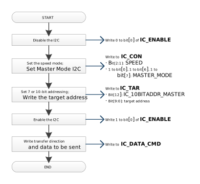
配置流程如下:
禁用 I2C:向 IC_ENABLE 寄存器写入 0。
向 IC_CON 寄存器写入,设置本次传输的速度模式(bit[2:1])。向 bit[0]、bit[6]、bit[7] 分别写入 1,以启用主机模块并禁用从机模块。
向 IC_TAR 寄存器写入要寻址的 I2C 设备地址。此寄存器还控制 I2C 是否发送 General Call 或 START BYTE 命令。寻址模式由 IC_10BITADDR_MASTER 位(bit[12])控制,无论是 7 位还是 10 位。
启用 I2C:向 IC_ENABLE 寄存器写入 1。
向 IC_DATA_CMD 寄存器写入传输方向和要发送的数据。在启用 I2C 之前写入 IC_DATA_CMD 寄存器的内容将会丢失,因为在 I2C 禁用时 FIFO 保持清空状态。
下面说明了主机模式下的 I2C 初始化配置。
动态更新 IC_TAR
I2C 作为主机时,目标地址(IC_TAR bit[9:0])和地址格式(IC_TAR.IC_10BITADDR_MASTER bit[12])可以动态更改,而无需禁用 I2C。从机模式则必须在更改地址之前禁用 I2C。
如需动态更新 IC_TAR 寄存器,需要满足以下条件:
I2C 未启用(IC_ENABLE =0);或
I2C 已启用(IC_ENABLE =1);并且
I2C 配置为主机模式(IC_CON [0]=1);并且
没有正在进行的传输(IC_STATUS [5]=0);并且
Tx FIFO 为空(IC_STATUS [2]=1)
主机发送和主机接收
要发送数据,请将数据写入 IC_DATA_CMD 寄存器的低 8 位(bit[7:0],即 Rx/Tx 数据缓冲区),将 bit[8](R/W 位)设为 0 表示写操作。
要发起读数据操作,请向 IC_DATA_CMD 寄存器的 R/W 位写入 1 表示读操作,向 bit[7:0] 写入“任意值”。
只要 Tx FIFO 中存在命令,I2C 主机就会不断发起传输。
如果在命令中将 STOP 位(IC_DATA_CMD 寄存器的 bit[9])置 1,I2C 在完成当前传输后会发送 STOP 条件。
I2C 支持在读、写之间动态切换。对于读、写复合格式传输,在改变数据传输方向的前一个命令中,必须将其 RESTART 位(IC_DATA_CMD 寄存器的 bit[10])设为 1。
从机模式
本节介绍 I2C 从机模式的功能描述,包括从机地址和软件操作流程。
双从机地址
I2C 作为从机时,具有双地址:
从机 1 支持 7 位或 10 位地址模式。
从机 2 仅支持 7 位地址模式。
设置 IC_CON [7:6] (
0x10) 来启用从机 1 或从机 2。从机 1 地址在 IC_SAR (
0x08) 中设置,支持 7 位或 10 位。从机 2 地址在 IC_SAR2 (
0xF4) 中设置,仅支持 7 位。IC_CON [3] (
0x10) IC_10BITADDR_SLAVE 控制 I2C 是响应 7 位还是 10 位地址。如果从机 1 和从机 2 都被启用,匹配地址的那个将响应 ACK。
操作流程
本节讨论从机模式的操作流程。
初始化配置
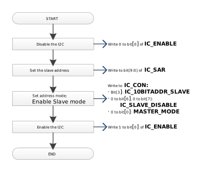
要将 I2C 用作从机,请执行以下步骤:
禁用 I2C:向 IC_ENABLE 寄存器的 bit[0] 写入 0。
设置从机地址:写入 IC_SAR 寄存器(bit[9:0])。这是 I2C 响应的地址。
配置 IC_CON 寄存器:设置 bit[3] 选择 7 位或 10 位地址模式。向 bit[6] 和 bit[7] (IC_SLAVE_DISABLE) 分别写入 0,向 bit[0] (MASTER_MODE) 写入 0,使能仅从机模式下的 I2C。
使能 I2C:向 IC_ENABLE 寄存器的 bit[0] 写入 1。
备注
从机和主机不必配置为相同的地址类型(即不要求双方同为 7 位或 10 位)。例如,从机可以配置为 7 位寻址,主机配置为 10 位寻址,反之亦然。
下图说明了从机模式下的 I2C 初始化配置。
从机发送单个字节的流程
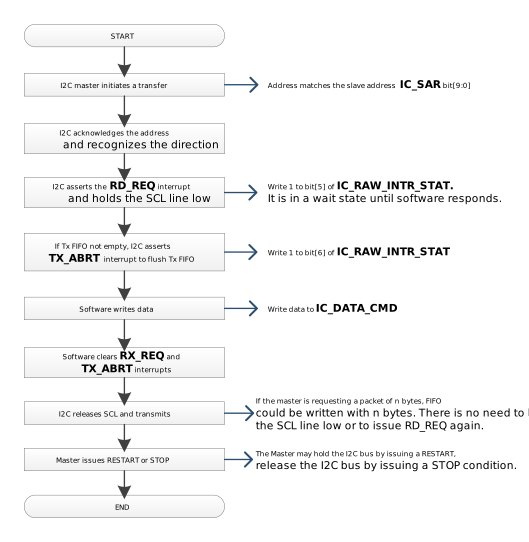
当 I2C 主机设备寻址此 I2C 设备并请求读取数据时,此 I2C 设备工作在从机发送模式,执行以下步骤:
主机发起 I2C 传输,其地址与 I2C 的 IC_SAR 寄存器中的从机地址匹配。
I2C 对地址进行应答,并识别传输方向。
I2C 触发 RD_REQ 中断(IC_RAW_INTR_STAT 寄存器的 bit[5])并将 SCL 线拉低。它处于等待状态,直到软件响应。
读取 IC_RAW_INTR_STAT [5] (RD_REQ 位) 值为 1 ,等效于 RD_REQ 中断被触发。
软件必须采取行动以满足 I2C 传输。
如果在接收到读取请求之前 Tx FIFO 中有任何剩余数据,则 I2C 触发 TX_ABRT 中断(IC_RAW_INTR_STAT 寄存器的 bit[6])以清空 Tx FIFO 中的旧数据。
备注
由于每当触发 TX_ABRT 中断时,I2C 的 Tx FIFO 就会被强制进入清空/复位状态,因此软件必须通过读 IC_CLR_TX_ABRT 寄存器来释放 I2C 的这种状态,然后才能尝试写入 Tx FIFO。有关更多详细信息,请参阅寄存器 IC_RAW_INTR_STAT。
读 IC_RAW_INTR_STAT [6] (TX_ABRT 位) 值为 1 ,表示 TX_ABRT 中断被触发。
软件无需采取进一步行动。
软件向 IC_DATA_CMD 寄存器写入数据(向 bit[8] 写入 0 以表示写操作)。
软件清除 IC_RAW_INTR_STAT 寄存器的 RD_REQ 和 TX_ABRT 中断。
I2C 释放 SCL 并发送该字节。
主机可以通过发出 RESTART 条件来保持 I2C 总线,或者通过发出 STOP 条件来释放总线。
下图说明了从机模式下的 I2C 数据传输。
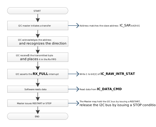
从机接收单个字节的流程
当总线上的另一个 I2C 主机设备寻址 I2C 并发送数据时,I2C 工作在从机接收模式,执行以下步骤:
另一个 I2C 主机设备发起 I2C 传输,其地址与 I2C 的 IC_SAR 寄存器中的从机地址匹配。
I2C 应答发送的地址并识别传输方向,表示 I2C 工作在从机接收模式。
I2C 接收发送的字节并将其放入 RX FIFO。
备注
当接收一个字节时,如果 RX FIFO 已满则会溢出,而 I2C 硬件将继续进行后续的传输。由于没有生成 NACK,需要通过软件检测 I2C FIFO 溢出(通过 IC_INTR_STAT 寄存器中的 RX_OVER 位)并尽快采取适当操作避免丢数据。
I2C 触发 RX_FULL 中断(IC_RAW_INTR_STAT [2] 寄存器)。
如果 RX_FULL 中断被屏蔽,由于将 IC_INTR_MASK [2] 寄存器设置为 0 或将 IC_TX_TL 设置为大于 0 的值,则建议软件轮询 IC_STATUS 寄存器。如果读到 IC_STATUS bit[3] (RFNE) 为 1,软件必须将其视为 RX_FULL 中断被触发。
软件从 IC_DATA_CMD 寄存器读取该字节(bit[7:0])。
主机设备可以通过发出 RESTART 条件来继续占用 I2C 总线,或者通过发出 STOP 条件来释放总线。
下图说明了从机模式下的 I2C 数据接收。
从机的批量传输操作
I2C 从机支持利用硬件 Tx FIFO 进行多字节批量传输。相比于每发一个字节就触发一次中断的传统做法,批量传输可以利用 FIFO 深度连续提供数据,从而显著降低总线延迟。此特性仅在从机工作于发送模式时有效。
批量传输的核心机制如下:
读请求:当主机发起读请求,若此时从机的 Tx FIFO 为空,硬件会自动将 SCL 线拉低(时钟延展)并触发读请求中断(RD_REQ),死等软件写入数据。
软件批量填入 FIFO:在处理 RD_REQ 中断时,软件需清除该中断,并可以一次性向 Tx FIFO 写入多个字节。
硬件连续发送:只要 Tx FIFO 中有可用数据,且主机持续回复 ACK,I2C 硬件就会在后台将数据连续发送出去,不再拉低 SCL,也不会产生额外的 RD_REQ 中断。
传输边界处理:
数据不足:如果 FIFO 数据已经发完,但主机回复 ACK 要求继续读取数据,从机会再次拉低 SCL 并触发 RD_REQ 中断。
数据过剩:如果软件写入 Tx FIFO 的字节数大于主机的实际需求量,当主机提早结束读取(回复 NACK 并 STOP)时,I2C 硬件会自动清空 Tx FIFO,无视并丢弃里面多余的残留字节。
备注
如果软件在设计上屏蔽了 RD_REQ 中断(IC_INTR_MASK 寄存器的 bit[5] 设置为 0),建议通过轮询 IC_RAW_INTR_STAT 寄存器的 bit[5] (RD_REQ) 来等效捕获主机的读取请求。
FIFO 管理
FIFO 状态与总线行为
如果 Tx FIFO 变空,I2C 不会生成 STOP;在这种情况下,该模块会将 SCL 线拉低,使总线暂停,直到 Tx FIFO 中有新的数据可用。只有在用户通过向 IC_DATA_CMD 寄存器的 bit[9] (STOP 位)写入 1 来明确请求时,才会生成 STOP 条件。下图显示了 IC_DATA_CMD 中的字段。有关更多详细信息,请参阅寄存器描述。

下图分别说明了 I2C 在分别作为主机发送器和主机接收器时 Tx FIFO 变空时的行为,以及 STOP 条件的生成。
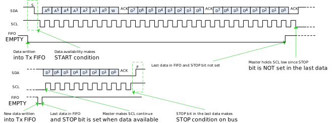
主机发送器 — Tx FIFO 空/STOP 生成
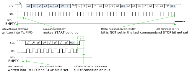
主机接收器 — Tx FIFO 空/STOP 生成
下图说明了用户可以控制 I2C 总线上 RESTART 条件生成的配置,分为主机写传输和读传输的场景。如果 IC_DATA_CMD 寄存器的 bit[10] (RESTART) 被置位,并且使能了重启功能(IC_RESTART_EN =1),则在向从机写入或读取数据字节之前会生成 RESTART。如果未使能重启功能,则会生成 STOP 后跟 START 来代替 RESTART。

主机发送器 — IC_DATA_CMD 的 RESTART 位被置位

主机接收器 — IC_DATA_CMD 的 RESTART 位被置位
当 IC_DATA_CMD 寄存器的 STOP 位被置位,并且 Tx FIFO 不为空时,如下图所示,分为主机写传输和读传输的场景。

主机发送器 — IC_DATA_CMD 的 STOP 位被置位/Tx FIFO 不为空

主机接收器 — IC_DATA_CMD 的 STOP 位被置位/Tx FIFO 不为空
SDA/SCL 数字滤波器
I2C 模块在 SDA 和 SCL 输入端提供了数字滤波功能,用于抑制总线上的高频噪声和信号毛刺,提高通信稳定性。
通过将 IC_FILTER 寄存器的 IC_DIG_FLTR_SEL 置为 1 来开启滤波器。
通过配置 IC_FILTER 寄存器的 IC_DIG_FLTR_DEG 来调整可被抑制的噪声或毛刺的宽度。该值越大,可抑制的毛刺持续时间越长,但滤波后的信号延迟也会更长。
持续时间小于
(IC_DIG_FLTR_DEG >> 1) + 1个时钟频率 (ic_clk) 周期的毛刺或噪声会被滤除。信号总延迟为
(IC_DIG_FLTR_DEG >> 1) + 3个 ic_clk 周期(其中包含了 2 个 ic_clk 周期的硬件固定开销)。
备注
在 I2C 滤波器的底层电路中,判定有效信号的阈值条件是“电平持续宽度是否大于配置宽度的一半”。 硬件逻辑通过对寄存器值除以 2 来获得该阈值,而数字电路中的“除以 2”操作等效于直接将数据右移一位。因此寄存器的最低位 (bit[0]) 会被直接丢弃,bit[0] 的值不会对滤波行为产生任何影响。
可编程 SDA 保持时间
在 I2C 通信中,为了确保接收方能正确读取数据,发送方必须在 SCL 下降沿之后,将 SDA 上的电平保持一段时间(即 SDA 保持时间)。
在配置 I2C 的 SDA 保持时间时,实际生效的时钟周期数会根据 I2C 当前所处的角色以及传输阶段有所不同。主要取决于 IC_SDA_HOLD 寄存器配置值与 数字滤波器的延迟。具体规则如下表所示:
角色 |
通信阶段 |
时钟来源 |
实际 SDA 保持时间 (ic_clk 周期数) |
|---|---|---|---|
主机 |
发送地址 |
外部总线 SCL (需经过数字滤波,应对仲裁) |
MAX ( IC_DIG_FLTR_DEG >> 1 + 5, IC_SDA_HOLD ) |
主机 |
发送数据 |
内部生成 SCL (直接驱动总线,无滤波延迟) |
IC_SDA_HOLD |
从机 |
发送数据 |
外部总线 SCL (需经过数字滤波,被动跟随) |
MAX ( IC_DIG_FLTR_DEG >> 1 + 5, IC_SDA_HOLD ) |
备注
数据的第 8 位不受 IC_SDA_HOLD 控制,因为在第 8 个 SCL 时钟下降沿之后,接收器控制 SDA 线来响应 ACK 或 NACK。
IC_SDA_HOLD 寄存器只能在 I2C 被禁用时 (IC_ENABLE = 0) 修改。
根据 I2C-Bus specification version2.1 的表 5,保持时间的最大值在 SS 模式下为 3.45us,在 FS 模式下为 0.9us。根据表 7,HS 模式下,保持时间的最大值在总线负载为 100pf 时为 70ns,总线负载为 400pf 时为 150ns。
DMA 控制器接口
I2C 具有可选的内置 DMA 功能,具备一个与 DMA 控制器连接的握手接口,用于请求和控制传输。
通过 DMA 接口进行内存和 IC_DATA_CMD 寄存器之间的数据传输,I2C 可以在不占用 CPU 资源的情况下高效地处理数据传输。
启用 DMA 控制器接口
要启用 I2C 的 DMA 控制器接口,需配置 DMA 控制寄存器 (IC_DMA_CR):
向 IC_DMA_CR 寄存器的 TDMAE 位写入 1,启用 I2C Tx DMA 握手接口。
向 IC_DMA_CR 寄存器的 RDMAE 位写入 1,启用 I2C Rx DMA 握手接口。
Tx FIFO 阈值
在 I2C 串行传输期间,只要 Tx FIFO 中的数据条目数小于或等于 DMA 发送数据量寄存器 (IC_DMA_TDLR) 的值,就会向 DMA 控制器发出 Tx FIFO 写入请求。DMA 即以突发(Burst)方式向 Tx FIFO 补充数据。
备注
防下溢(Underflow)机制:必须确保 DMA 搬运数据的频率足够高,防止 Tx FIFO 提前耗尽。一旦发生 FIFO 下溢,硬件会在 I2C 总线上错误地插入一个 STOP 信号,导致通信意外中断。因此用户必须为应用分配一个合理的发送阈值。
为了实现最佳的总线操作效率,尽量减少每块传输次数的同时避免下溢,DMA 的目标端突发传输大小 (DMA.CTLx.DEST_MSIZE) 必须等于触发请求时的 Tx FIFO 剩余可用空间;计算公式如下:
DMA.CTLx.DEST_MSIZE = I2C.FIFO_DEPTH - I2C.IC_DMA_TDLR
Rx FIFO 阈值
在 I2C 串行接收期间,只要 Rx FIFO 中的数据条目数 等于或高于 接收阈值(即 IC_DMA_RDLR + 1),就会向 DMA 控制器发出 Rx FIFO 读取请求。DMA 会以突发方式从 Rx FIFO 获取长度为 CTLx.SRC_MSIZE 的数据。
备注
防溢出(Overflow)机制:DMA 必须足够及时地将数据从 Rx FIFO 取走,以防 Rx FIFO 被后续到达的数据填满,从而导致新数据溢出和丢失。
与发送阈值策略类似,为了最大限度降低溢出概率并达到最佳性能,DMA 的源端突发读取大小 (DMA.CTLx.SRC_MSIZE) 应精确等于接收阈值的触发量;计算公式如下:
DMA.CTLx.SRC_MSIZE = I2C.IC_DMA_RDLR + 1
DMA 传输控制寄存器
I2C 模块提供了用于控制 DMA 传输过程的寄存器:IC_DMA_CMD 和 IC_DMA_DATA_LEN 寄存器。其中 IC_DMA_DATA_LEN 用于配置传输的数据长度。IC_DMA_CMD 寄存器包含几个字段:
ENABLE用于使能 I2C DMA 模式。CMD用于控制主机的传输方向。RESTART用于在最后一个数据传输后是否驱动 RESTART 信号。STOP用于在最后一个数据传输后是否驱动 STOP 信号。
下面介绍主机和从机模式下的使用方法。
主机模式
I2C DMA Tx 配置步骤如下:
初始化 GDMA Tx 通道:配置源地址(内存)、目标地址(I2C Tx FIFO)及传输完成中断 ISR;
配置 I2C DMA 控制寄存器:向 IC_DMA_DATA_LEN 寄存器中写入待发送总字节数;将 IC_DMA_CMD 寄存器的 DMODE_ENABLE 和 DMODE_STOP 位设置为 1,使 I2C 在最后一字节后自动产生 STOP 条件;
使能 Tx DMA(IC_DMA_CR 寄存器 TDMAE 位),开始发送,将在 FIFO 数据量低于 IC_DMA_TDLR 时触发 DMA Tx。
在 GDMA Tx 中断 ISR 中应执行以下操作:
轮询 IC_STATUS.TFE 等待 Tx FIFO 清空,以确保所有数据都已发送到总线;
若仍有剩余数据未发送完成,重新启动 DMA 传输
全部完成后释放 GDMA 通道,结束传输
I2C DMA Rx 配置步骤与 Tx 类似:
初始化 GDMA Rx 通道:配置源地址(I2C Rx FIFO)、目标地址(内存)及传输完成中断 ISR;
配置 I2C DMA 控制寄存器:向 IC_DMA_DATA_LEN 寄存器中写入待接收字节数;将 IC_DMA_CMD 寄存器的 DMODE_ENABLE、DMODE_STOP 与 DMODE_CMD 位设置为 1,使 I2C 自动向总线循环发出读命令;
使能 Rx DMA(IC_DMA_CR 寄存器 RDMAE 位),开始接收,将在 FIFO 数据量超过 IC_DMA_RDLR 时触发 DMA Rx。
在 GDMA Rx 中断 ISR 中:
若仍有剩余数据,更新 GDMA 目标地址和块大小后重新启动传输
全部完成后释放 GDMA 通道,结束传输
从机模式
步骤与主机模式类似,存在以下差异:
在使能 Rx DMA 之前,要轮询 IC_RAW_INTR_STAT.RX_FULL,等待 Rx FIFO 已满,再开始接收。
在使能 Tx DMA 之前,要轮询 IC_RAW_INTR_STAT.RD_REQ,等待主机发出读请求,再开始发送。
无需配置 DMODE_STOP 位 和 DMODE_CMD 位。
不支持。
不支持。
不支持。
不支持。
不支持。
I2C 具有可选的内置 DMA 功能,具备一个与 DMA 控制器连接的握手接口,用于请求和控制传输。
通过 DMA 接口进行内存和 IC_DATA_CMD 寄存器之间的数据传输,I2C 可以在不占用 CPU 资源的情况下高效地处理数据传输。
启用 DMA 控制器接口
要启用 I2C 的 DMA 控制器接口,需配置 DMA 控制寄存器 (IC_DMA_CR):
向 IC_DMA_CR 寄存器的 TDMAE 位写入 1,启用 I2C Tx DMA 握手接口。
向 IC_DMA_CR 寄存器的 RDMAE 位写入 1,启用 I2C Rx DMA 握手接口。
Tx FIFO 阈值
在 I2C 串行传输期间,只要 Tx FIFO 中的数据条目数小于或等于 DMA 发送数据量寄存器 (IC_DMA_TDLR) 的值,就会向 DMA 控制器发出 Tx FIFO 写入请求。DMA 即以突发(Burst)方式向 Tx FIFO 补充数据。
备注
防下溢(Underflow)机制:必须确保 DMA 搬运数据的频率足够高,防止 Tx FIFO 提前耗尽。一旦发生 FIFO 下溢,硬件会在 I2C 总线上错误地插入一个 STOP 信号,导致通信意外中断。因此用户必须为应用分配一个合理的发送阈值。
为了实现最佳的总线操作效率,尽量减少每块传输次数的同时避免下溢,DMA 的目标端突发传输大小 (DMA.CTLx.DEST_MSIZE) 必须等于触发请求时的 Tx FIFO 剩余可用空间;计算公式如下:
DMA.CTLx.DEST_MSIZE = I2C.FIFO_DEPTH - I2C.IC_DMA_TDLR
Rx FIFO 阈值
在 I2C 串行接收期间,只要 Rx FIFO 中的数据条目数 等于或高于 接收阈值(即 IC_DMA_RDLR + 1),就会向 DMA 控制器发出 Rx FIFO 读取请求。DMA 会以突发方式从 Rx FIFO 获取长度为 CTLx.SRC_MSIZE 的数据。
备注
防溢出(Overflow)机制:DMA 必须足够及时地将数据从 Rx FIFO 取走,以防 Rx FIFO 被后续到达的数据填满,从而导致新数据溢出和丢失。
与发送阈值策略类似,为了最大限度降低溢出概率并达到最佳性能,DMA 的源端突发读取大小 (DMA.CTLx.SRC_MSIZE) 应精确等于接收阈值的触发量;计算公式如下:
DMA.CTLx.SRC_MSIZE = I2C.IC_DMA_RDLR + 1
DMA 传输控制寄存器
I2C 模块提供了用于控制 DMA 传输过程的寄存器:IC_DMA_CMD 和 IC_DMA_DATA_LEN 寄存器。其中 IC_DMA_DATA_LEN 用于配置传输的数据长度。IC_DMA_CMD 寄存器包含几个字段:
ENABLE用于使能 I2C DMA 模式。CMD用于控制主机的传输方向。RESTART用于在最后一个数据传输后是否驱动 RESTART 信号。STOP用于在最后一个数据传输后是否驱动 STOP 信号。
下面介绍主机和从机模式下的使用方法。
主机模式
I2C DMA Tx 配置步骤如下:
初始化 GDMA Tx 通道:配置源地址(内存)、目标地址(I2C Tx FIFO)及传输完成中断 ISR;
配置 I2C DMA 控制寄存器:向 IC_DMA_DATA_LEN 寄存器中写入待发送总字节数;将 IC_DMA_CMD 寄存器的 DMODE_ENABLE 和 DMODE_STOP 位设置为 1,使 I2C 在最后一字节后自动产生 STOP 条件;
使能 Tx DMA(IC_DMA_CR 寄存器 TDMAE 位),开始发送,将在 FIFO 数据量低于 IC_DMA_TDLR 时触发 DMA Tx。
在 GDMA Tx 中断 ISR 中应执行以下操作:
轮询 IC_STATUS.TFE 等待 Tx FIFO 清空,以确保所有数据都已发送到总线;
若仍有剩余数据未发送完成,重新启动 DMA 传输
全部完成后释放 GDMA 通道,结束传输
I2C DMA Rx 配置步骤与 Tx 类似:
初始化 GDMA Rx 通道:配置源地址(I2C Rx FIFO)、目标地址(内存)及传输完成中断 ISR;
配置 I2C DMA 控制寄存器:向 IC_DMA_DATA_LEN 寄存器中写入待接收字节数;将 IC_DMA_CMD 寄存器的 DMODE_ENABLE、DMODE_STOP 与 DMODE_CMD 位设置为 1,使 I2C 自动向总线循环发出读命令;
使能 Rx DMA(IC_DMA_CR 寄存器 RDMAE 位),开始接收,将在 FIFO 数据量超过 IC_DMA_RDLR 时触发 DMA Rx。
在 GDMA Rx 中断 ISR 中:
若仍有剩余数据,更新 GDMA 目标地址和块大小后重新启动传输
全部完成后释放 GDMA 通道,结束传输
从机模式
步骤与主机模式类似,存在以下差异:
在使能 Rx DMA 之前,要轮询 IC_RAW_INTR_STAT.RX_FULL,等待 Rx FIFO 已满,再开始接收。
在使能 Tx DMA 之前,要轮询 IC_RAW_INTR_STAT.RD_REQ,等待主机发出读请求,再开始发送。
无需配置 DMODE_STOP 位 和 DMODE_CMD 位。
I2C 具有可选的内置 DMA 功能,具备一个与 DMA 控制器连接的握手接口,用于请求和控制传输。
通过 DMA 接口进行内存和 IC_DATA_CMD 寄存器之间的数据传输,I2C 可以在不占用 CPU 资源的情况下高效地处理数据传输。
启用 DMA 控制器接口
要启用 I2C 的 DMA 控制器接口,需配置 DMA 控制寄存器 (IC_DMA_CR):
向 IC_DMA_CR 寄存器的 TDMAE 位写入 1,启用 I2C Tx DMA 握手接口。
向 IC_DMA_CR 寄存器的 RDMAE 位写入 1,启用 I2C Rx DMA 握手接口。
Tx FIFO 阈值
在 I2C 串行传输期间,只要 Tx FIFO 中的数据条目数小于或等于 DMA 发送数据量寄存器 (IC_DMA_TDLR) 的值,就会向 DMA 控制器发出 Tx FIFO 写入请求。DMA 即以突发(Burst)方式向 Tx FIFO 补充数据。
备注
防下溢(Underflow)机制:必须确保 DMA 搬运数据的频率足够高,防止 Tx FIFO 提前耗尽。一旦发生 FIFO 下溢,硬件会在 I2C 总线上错误地插入一个 STOP 信号,导致通信意外中断。因此用户必须为应用分配一个合理的发送阈值。
为了实现最佳的总线操作效率,尽量减少每块传输次数的同时避免下溢,DMA 的目标端突发传输大小 (DMA.CTLx.DEST_MSIZE) 必须等于触发请求时的 Tx FIFO 剩余可用空间;计算公式如下:
DMA.CTLx.DEST_MSIZE = I2C.FIFO_DEPTH - I2C.IC_DMA_TDLR
Rx FIFO 阈值
在 I2C 串行接收期间,只要 Rx FIFO 中的数据条目数 等于或高于 接收阈值(即 IC_DMA_RDLR + 1),就会向 DMA 控制器发出 Rx FIFO 读取请求。DMA 会以突发方式从 Rx FIFO 获取长度为 CTLx.SRC_MSIZE 的数据。
备注
防溢出(Overflow)机制:DMA 必须足够及时地将数据从 Rx FIFO 取走,以防 Rx FIFO 被后续到达的数据填满,从而导致新数据溢出和丢失。
与发送阈值策略类似,为了最大限度降低溢出概率并达到最佳性能,DMA 的源端突发读取大小 (DMA.CTLx.SRC_MSIZE) 应精确等于接收阈值的触发量;计算公式如下:
DMA.CTLx.SRC_MSIZE = I2C.IC_DMA_RDLR + 1
DMA 传输控制寄存器
I2C 模块提供了用于控制 DMA 传输过程的寄存器:IC_DMA_CMD 和 IC_DMA_DATA_LEN 寄存器。其中 IC_DMA_DATA_LEN 用于配置传输的数据长度。IC_DMA_CMD 寄存器包含几个字段:
ENABLE用于使能 I2C DMA 模式。CMD用于控制主机的传输方向。RESTART用于在最后一个数据传输后是否驱动 RESTART 信号。STOP用于在最后一个数据传输后是否驱动 STOP 信号。
下面介绍主机和从机模式下的使用方法。
主机模式
I2C DMA Tx 配置步骤如下:
初始化 GDMA Tx 通道:配置源地址(内存)、目标地址(I2C Tx FIFO)及传输完成中断 ISR;
配置 I2C DMA 控制寄存器:向 IC_DMA_DATA_LEN 寄存器中写入待发送总字节数;将 IC_DMA_CMD 寄存器的 DMODE_ENABLE 和 DMODE_STOP 位设置为 1,使 I2C 在最后一字节后自动产生 STOP 条件;
使能 Tx DMA(IC_DMA_CR 寄存器 TDMAE 位),开始发送,将在 FIFO 数据量低于 IC_DMA_TDLR 时触发 DMA Tx。
在 GDMA Tx 中断 ISR 中应执行以下操作:
轮询 IC_STATUS.TFE 等待 Tx FIFO 清空,以确保所有数据都已发送到总线;
若仍有剩余数据未发送完成,重新启动 DMA 传输
全部完成后释放 GDMA 通道,结束传输
I2C DMA Rx 配置步骤与 Tx 类似:
初始化 GDMA Rx 通道:配置源地址(I2C Rx FIFO)、目标地址(内存)及传输完成中断 ISR;
配置 I2C DMA 控制寄存器:向 IC_DMA_DATA_LEN 寄存器中写入待接收字节数;将 IC_DMA_CMD 寄存器的 DMODE_ENABLE、DMODE_STOP 与 DMODE_CMD 位设置为 1,使 I2C 自动向总线循环发出读命令;
使能 Rx DMA(IC_DMA_CR 寄存器 RDMAE 位),开始接收,将在 FIFO 数据量超过 IC_DMA_RDLR 时触发 DMA Rx。
在 GDMA Rx 中断 ISR 中:
若仍有剩余数据,更新 GDMA 目标地址和块大小后重新启动传输
全部完成后释放 GDMA 通道,结束传输
从机模式
步骤与主机模式类似,存在以下差异:
在使能 Rx DMA 之前,要轮询 IC_RAW_INTR_STAT.RX_FULL,等待 Rx FIFO 已满,再开始接收。
在使能 Tx DMA 之前,要轮询 IC_RAW_INTR_STAT.RD_REQ,等待主机发出读请求,再开始发送。
无需配置 DMODE_STOP 位 和 DMODE_CMD 位。
DMA 流控制器
I2C 模块支持使用 DMA 控制器(DMAC)或 I2C 硬件作为 DMA 的流控制器(Flow Controller),以应对数据长度已知/未知的不同应用场景:
使用 DMAC 作为流控制器(针对定长数据):需由软件提前将固定长度
block_size写入 DMAC。当 DMA 搬运的数据量达到设定值时,硬件自动结束本次 block 传输。使用 I2C 作为流控制器(针对变长数据):由 I2C 硬件判断何时终止传输。当 I2C 识别到接收末尾时,会主动拉高
rx_dma_last握手信号,强制通知 DMA 结束本次 block 传输。
针对不同的工作模式对上述两种流控制器的选择策略如下:
主机发送/接收
数据长度已知,使用 DMAC 作为流控制器。
从机发送
如果每次已知主机必然读取固定长度的数据,使用 DMAC。
主机可能在传输完预定长度之前提前发送 STOP 结束传输,这意味着从机视角的发送数据长度不固定。为应对这种情况,可以使用 I2C 作为流控制器。并开启 RX_DONE 中断,当主机提前终止通信时,可在此中断的 ISR 中执行软件重置和状态复位,避免后续传输错乱。
从机接收
如果数据长度未知,可使用 I2C 作为流控制器。
传输开始前,用户需配置 IC_RDMA_DAT_LEN 寄存器。I2C 在接收到该位数的最后一个有效字节前将会拉高 rx_dma_last 安全停止 DMA。
需开启 RXFIFO_TIMEOUT 中断,将在 RX FIFO empty 计时器超过阈值 I2C_RXFIFO_TIMEOUT_TH 时触发。中断触发后,硬件自动清除 IC_DMA_CR.RDMAE 以关闭 RX DMA 通道。如果随后有数据进入 RX FIFO,不会发起 dma_req。随后,用户应通过软件禁用 DMA。
寄存器
Base Address:
I2C0_REG : 0x41108000
I2C1_REG : 0x4110A000
Name |
Address offset |
Access |
Description |
|---|---|---|---|
000h |
R/W |
||
004h |
R/W |
||
008h |
R/W |
||
00Ch |
R/W |
||
010h |
R/W |
||
014h |
R/W |
||
018h |
R/W |
||
01Ch |
R/W |
||
020h |
R/W |
||
024h |
R/W |
||
028h |
R/W |
||
02Ch |
R |
||
030h |
R/W |
||
034h |
R |
||
038h |
R/W |
||
03Ch |
R/W |
||
040h |
R |
||
044h |
R |
||
048h |
R |
||
04Ch |
R |
||
050h |
R |
||
054h |
R |
||
058h |
R |
||
05Ch |
R |
||
060h |
R |
||
064h |
R |
||
068h |
R |
||
06Ch |
R/W |
||
070h |
R |
||
074h |
R |
||
078h |
R |
||
07Ch |
R/W |
||
080h |
R |
||
084h |
R/W |
||
088h |
R/W |
||
08Ch |
R/W |
||
090h |
R/W |
||
094h |
R/W |
||
098h |
R/W |
||
09Ch |
R |
||
0A0h |
R/W |
||
0A4h |
R/W |
||
0A8h |
R/W |
||
0ACh |
R |
||
0B0h |
R/W |
||
0B4h |
R/W |
||
0E4h |
R |
||
0E8h |
R |
||
0ECh |
R/W |
||
0F4h |
R/W |
||
0FCh |
R |
||
100h |
R |
REG_IC_CON
Name: I2C Control Register
Size: 32
Address offset: 000h
Read/write access: R/W
Bit |
Symbol |
Access |
INI |
Description |
|---|---|---|---|---|
31:8 |
RSVD |
R |
- |
Reserved |
7 |
IC_SLAVE_DISABLE_1 |
R/W |
0x0 |
This bit controls whether I2C has its slave2 (7-bit address) disabled.
|
6 |
IC_SLAVE_DISABLE_0 |
R/W |
0x0 |
This bit controls whether I2C has its slave1 (7-bit or 10-bit address) disabled.
|
5 |
IC_RESTATRT_EN |
R/W |
0x0 |
Determine whether RESTART conditions may be sent when acting as a master.
|
4 |
RSVD |
R |
- |
Reserved |
3 |
IC_10BITADDR_SLAVE |
R/W |
0x0 |
When acting as a slave, this bit controls whether the I2C responds to 7- or 10-bit addresses.
|
2:1 |
SPEED |
R/W |
0x0 |
These bits control at which speed the I2C operates; its setting is relevant only if one is operating the I2C in master mode.
|
0 |
MASTER_MODE |
R/W |
0x0 |
This bit controls whether the I2C master is enabled.
|
REG_IC_TAR
Name: I2C Target Address Register
Size: 32
Address offset: 004h
Read/write access: R/W
Bit |
Symbol |
Access |
INI |
Description |
|---|---|---|---|---|
31:13 |
RSVD |
R |
- |
Reserved |
12 |
IC_10BITADDR_MASTER |
R/W |
0x0 |
Control whether I2C starts its transfers in 7- or 10-bit addressing mode when acting as a master.
|
11 |
SPECIAL |
R/W |
0x0 |
This bit indicates whether software performs a General Call or START BYTE command.
|
10 |
GC_OR_START |
R/W |
0x0 |
If SPECIAL is set to 1, then this bit indicates whether a General Call or START BYTE command is to be performed by I2C. (ic_clk domain)
|
9:0 |
IC_TAR |
R/W |
0x10 |
This is the target address for any master transaction. When transmitting a General Call, these bits are ignored. To generate a START BYTE, the CPU needs to write only once into these bits. |
REG_IC_SAR
Name: I2C Slave Address Register
Size: 32
Address offset: 008h
Read/write access: R/W
Bit |
Symbol |
Access |
INI |
Description |
|---|---|---|---|---|
31:10 |
RSVD |
R |
- |
Reserved |
9:0 |
IC_SAR |
R/W |
0x11 |
The IC_SAR holds the slave address when the I2C is operating as slave1. For 7-bit addressing, only IC_SAR[6:0] is used. The register can be written only when the I2C interface is disabled, which corresponds to the IC_ENABLE register being set to 0. Writes at other times have no effect. |
REG_IC_HS_MAR
Name: I2C High Speed Master Mode Code Address Register
Size: 32
Address offset: 00Ch
Read/write access: R/W
Bit |
Symbol |
Access |
INI |
Description |
|---|---|---|---|---|
31:3 |
RSVD |
R |
- |
Reserved |
2:0 |
IC_HS_MAR |
R/W |
0x0 |
This bit field holds the value of the I2C HS mode master code. HS-mode master codes are reserved 8-bit codes (00001xxx) that are not used for slave addressing or other purposes. This register can be written only when the I2C interface is disabled, which corresponds to the IC_ENABLE register being set to 0. Write at other times have no effect. |
REG_IC_DATA_CMD
Name: I2C Rx/Tx Data Buffer and Command Register
Size: 32
Address offset: 010h
Read/write access: R/W
Bit |
Symbol |
Access |
INI |
Description |
|---|---|---|---|---|
31:12 |
RSVD |
R |
- |
Reserved |
11 |
NULL_DATA |
R/W |
0x0 |
|
10 |
CMD_RESTART |
R/W |
0x0 |
This bit controls whether a RESTART is issued after the byte is sent or received.
|
9 |
CMD_STOP |
R/W |
0x0 |
This bit controls whether a STOP is issued after the byte is sent or received.
|
8 |
CMD_RW |
R/W |
0x0 |
This bit controls whether a read or write is performed. This bit does not control the direction when the I2C acts as a slave. It controls only the direction when it acts as a master.
|
7:0 |
IC_DATA |
R/W |
0x0 |
This register contains the data to be transmitted or received on the I2C bus. If you are writing to this register and want to perform a read, these bits are ignored by the I2C. However, when you read this register, these bits return the value of data received on the I2C interface. |
REG_IC_SS_SCL_HCNT
Name: Standard Speed I2C Clock SCL High Count Register
Size: 32
Address offset: 014h
Read/write access: R/W
Bit |
Symbol |
Access |
INI |
Description |
|---|---|---|---|---|
31:16 |
RSVD |
R |
- |
Reserved |
15:0 |
IC_SS_SCL_HCNT |
R/W |
0x0190 |
This register sets the SCL clock high-period count for standard speed. This register must be set before any I2C bus transaction can take place to ensure proper I/O timing. This register can be written only when the I2C interface is disabled which corresponds to the IC_ENABLE register being set to 0. Writes at other times have no effect. |
REG_IC_SS_SCL_LCNT
Name: Standard Speed I2C Clock SCL Low Count Register
Size: 32
Address offset: 018h
Read/write access: R/W
Bit |
Symbol |
Access |
INI |
Description |
|---|---|---|---|---|
31:16 |
RSVD |
R |
- |
Reserved |
15:0 |
IC_SS_SCL_LCNT |
R/W |
0x01D6 |
This register sets the SCL clock low-period count for standard speed. This register must be set before any I2C bus transaction can take place to ensure proper I/O timing. This register can be written only when the I2C interface is disabled which corresponds to the IC_ENABLE register being set to 0. Writes at other times have no effect. |
REG_IC_FS_SCL_HCNT
Name: Fast Speed I2C Clock SCL High Count Register
Size: 32
Address offset: 01Ch
Read/write access: R/W
Bit |
Symbol |
Access |
INI |
Description |
|---|---|---|---|---|
31:16 |
RSVD |
R |
- |
Reserved |
15:0 |
IC_FS_SCL_HCNT |
R/W |
0x003C |
This register sets the SCL clock high-period count for fast speed. This register must be set before any I2C bus transaction can take place to ensure proper I/O timing. This register can be written only when the I2C interface is disabled which corresponds to the IC_ENABLE register being set to 0. Writes at other times have no effect. |
REG_IC_FS_SCL_LCNT
Name: Fast Speed I2C Clock SCL Low Count Register
Size: 32
Address offset: 020h
Read/write access: R/W
Bit |
Symbol |
Access |
INI |
Description |
|---|---|---|---|---|
31:16 |
RSVD |
R |
- |
Reserved |
15:0 |
IC_FS_SCL_LCNT |
R/W |
0x0082 |
This register sets the SCL clock low-period count for fast speed. This register must be set before any I2C bus transaction can take place to ensure proper I/O timing. This register can be written only when the I2C interface is disabled which corresponds to the IC_ENABLE register being set to 0. Writes at other times have no effect. |
REG_IC_HS_SCL_HCNT
Name: High Speed I2C Clock SCL High Count Register
Size: 32
Address offset: 024h
Read/write access: R/W
Bit |
Symbol |
Access |
INI |
Description |
|---|---|---|---|---|
31:16 |
RSVD |
R |
- |
Reserved |
15:0 |
IC_HS_SCL_HCNT |
R/W |
0x0006 |
This register sets the SCL clock high-period count for high speed. This register must be set before any I2C bus transaction can take place to ensure proper I/O timing. This register can be written only when the I2C interface is disabled which corresponds to the IC_ENABLE register being set to 0. Writes at other times have no effect. The SCL High time depends on the loading of the bus. For 100pF loading, the SCL High time is 60ns; for 400pF loading, the SCL High time is 120ns. |
REG_IC_HS_SCL_LCNT
Name: High Speed I2C Clock SCL Low Count Register
Size: 32
Address offset: 028h
Read/write access: R/W
Bit |
Symbol |
Access |
INI |
Description |
|---|---|---|---|---|
31:16 |
RSVD |
R |
- |
Reserved |
15:0 |
IC_HS_SCL_LCNT |
R/W |
0x0010 |
This register sets the SCL clock low-period count for high speed. This register must be set before any I2C bus transaction can take place to ensure proper I/O timing. This register can be written only when the I2C interface is disabled which corresponds to the IC_ENABLE register being set to 0. Writes at other times have no effect. The SCL Low time depends on the loading of the bus. For 100pF loading, the SCL High time is 160ns; for 400pF loading, the SCL High time is 320ns. |
REG_IC_INTR_STAT
Name: I2C Interrupt Status Register
Size: 32
Address offset: 02Ch
Read/write access: R
Bit |
Symbol |
Access |
INI |
Description |
|---|---|---|---|---|
31:14 |
RSVD |
R |
- |
Reserved |
13 |
R_LP_WAKE_2 |
R |
0x0 |
Refer to I2C Raw Interrupt Status Register (IC_RAW_INTR_STAT) for a detailed description of this bit. |
12 |
R_LP_WAKE_1 |
R |
0x0 |
Refer to I2C Raw Interrupt Status Register (IC_RAW_INTR_STAT) for a detailed description of this bit. |
11 |
R_GEN_CALL |
R |
0x0 |
Refer to I2C Raw Interrupt Status Register (IC_RAW_INTR_STAT) for a detailed description of this bit. |
10 |
R_START_DET |
R |
0x0 |
Refer to I2C Raw Interrupt Status Register (IC_RAW_INTR_STAT) for a detailed description of this bit. |
9 |
R_STOP_DET |
R |
0x0 |
Refer to I2C Raw Interrupt Status Register (IC_RAW_INTR_STAT) for a detailed description of this bit. |
8 |
R_ACTIVITY |
R |
0x0 |
Refer to I2C Raw Interrupt Status Register (IC_RAW_INTR_STAT) for a detailed description of this bit. |
7 |
R_RX_DONE |
R |
0x0 |
Refer to I2C Raw Interrupt Status Register (IC_RAW_INTR_STAT) for a detailed description of this bit. |
6 |
R_TX_ABRT |
R |
0x0 |
Refer to I2C Raw Interrupt Status Register (IC_RAW_INTR_STAT) for a detailed description of this bit. |
5 |
R_RD_REQ |
R |
0x0 |
Refer to I2C Raw Interrupt Status Register (IC_RAW_INTR_STAT) for a detailed description of this bit. |
4 |
R_TX_EMPTY |
R |
0x0 |
Refer to I2C Raw Interrupt Status Register (IC_RAW_INTR_STAT) for a detailed description of this bit. |
3 |
R_TX_OVER |
R |
0x0 |
Refer to I2C Raw Interrupt Status Register (IC_RAW_INTR_STAT) for a detailed description of this bit. |
2 |
R_RX_FULL |
R |
0x0 |
Refer to I2C Raw Interrupt Status Register (IC_RAW_INTR_STAT) for a detailed description of this bit. |
1 |
R_RX_OVER |
R |
0x0 |
Refer to I2C Raw Interrupt Status Register (IC_RAW_INTR_STAT) for a detailed description of this bit. |
0 |
R_RX_UNDER |
R |
0x0 |
Refer to I2C Raw Interrupt Status Register (IC_RAW_INTR_STAT) for a detailed description of this bit. |
REG_IC_INTR_MASK
Name: I2C Interrupt Mask Register
Size: 32
Address offset: 030h
Read/write access: R/W
Bit |
Symbol |
Access |
INI |
Description |
|---|---|---|---|---|
31:14 |
RSVD |
R |
- |
Reserved |
13 |
M_LP_WAKE_2 |
R/W |
0x0 |
This bit masks the corresponding interrupt status bit in the IC_INTR_STAT register. |
12 |
M_LP_WAKE_1 |
R/W |
0x0 |
This bit masks the corresponding interrupt status bit in the IC_INTR_STAT register. |
11 |
M_GEN_CALL |
R/W |
0x0 |
This bit masks the corresponding interrupt status bit in the IC_INTR_STAT register. |
10 |
M_START_DET |
R/W |
0x0 |
This bit masks the corresponding interrupt status bit in the IC_INTR_STAT register. |
9 |
M_STOP_DET |
R/W |
0x0 |
This bit masks the corresponding interrupt status bit in the IC_INTR_STAT register. |
8 |
M_ACTIVITY |
R/W |
0x0 |
This bit masks the corresponding interrupt status bit in the IC_INTR_STAT register. |
7 |
M_RX_DONE |
R/W |
0x0 |
This bit masks the corresponding interrupt status bit in the IC_INTR_STAT register. |
6 |
M_TX_ABRT |
R/W |
0x0 |
This bit masks the corresponding interrupt status bit in the IC_INTR_STAT register. |
5 |
M_RD_REQ |
R/W |
0x0 |
This bit masks the corresponding interrupt status bit in the IC_INTR_STAT register. |
4 |
M_TX_EMPTY |
R/W |
0x0 |
This bit masks the corresponding interrupt status bit in the IC_INTR_STAT register. |
3 |
M_TX_OVER |
R/W |
0x0 |
This bit masks the corresponding interrupt status bit in the IC_INTR_STAT register. |
2 |
M_RX_FULL |
R/W |
0x0 |
This bit masks the corresponding interrupt status bit in the IC_INTR_STAT register. |
1 |
M_RX_OVER |
R/W |
0x0 |
This bit masks the corresponding interrupt status bit in the IC_INTR_STAT register. |
0 |
M_RX_UNDER |
R/W |
0x0 |
This bit masks the corresponding interrupt status bit in the IC_INTR_STAT register. |
REG_IC_RAW_INTR_STAT
Name: I2C Raw Interrupt Status Register
Size: 32
Address offset: 034h
Read/write access: R
Bit |
Symbol |
Access |
INI |
Description |
|---|---|---|---|---|
31:14 |
RSVD |
R |
- |
Reserved |
13 |
LP_WAKE_2 |
R |
0x0 |
Set when address SAR_2 matches with address sending on I2C BUS. |
12 |
LP_WAKE_1 |
R |
0x0 |
Set when address SAR matches with address sending on I2C BUS. |
11 |
GEN_CALL |
R |
0x0 |
Set only when a General Call address is received and it is acknowledged. |
10 |
START_DET |
R |
0x0 |
Indicate whether a START or RESTART condition has occurred on the I2C interface regardless of whether I2C is operating in slave or master mode. |
9 |
STOP_DET |
R |
0x0 |
Indicate whether a STOP condition has occurred on the I2C interface regardless of whether I2C is operating in slave or master mode. |
8 |
ACTIVITY |
R |
0x0 |
This bit captures I2C activity. |
7 |
RX_DONE |
R |
0x0 |
When the I2C is acting as a slave-transmitter, this bit is set to 1 if the master does not acknowledge a transmitted byte. This occurs on the last byte of the transmission, indicating that the transmission is done. |
6 |
TX_ABRT |
R |
0x0 |
This bit indicates if I2C as a transmitter, is unable to complete the intended actions on the contents of the transmit FIFO. This situation can occur both as an I2C master or an I2C slave, and is referred to as a 'transmit abort'.
|
5 |
RD_REQ |
R |
0x0 |
This bit is set to 1 when I2C is acting as a slave and another I2C master is attempting to read data from I2C. The I2C holds the I2C bus in a wait state (SCL=0) until this interrupt is serviced, which means that the slave has been addressed by a remote master that is asking for data to be transferred. The processor must respond to this interrupt and then write the requested data to the IC_DATA_CMD register. |
4 |
TX_EMPTY |
R |
0x0 |
This bit is set to 1 when the transmit buffer is at or below the threshold value set in the IC_TX_TL register. It is automatically cleared by hardware when the buffer level goes above the threshold. |
3 |
TX_OVER |
R |
0x0 |
Set during transmit if the transmit buffer is filled to IC_TX_BUFFER_DEPTH and the processor attempts to issue another I2C command by writing to the IC_DATA_CMD register. |
2 |
RX_FULL |
R |
0x0 |
Set when the receive buffer goes above the RX_TL threshold in the IC_RX_TL register. It is automatically cleared by hardware when buffer level is equal to or less than the threshold. |
1 |
RX_OVER |
R |
0x0 |
Not used. Set if the receive buffer is completely filled to IC_RX_BUFFER_DEPTH and an additional byte is received from an external I2C device. |
0 |
RX_UNDER |
R |
0x0 |
Set if the processor attempts to read the receive buffer when it is empty by reading from the IC_DATA_CMD register. |
REG_IC_RX_TL
Name: I2C Receive FIFO Threshold Register
Size: 32
Address offset: 038h
Read/write access: R/W
Bit |
Symbol |
Access |
INI |
Description |
|---|---|---|---|---|
31:8 |
RSVD |
R |
- |
Reserved |
7:0 |
IC_RX_0_TL |
R/W |
0x0 |
Receive FIFO Threshold Level. Control the level of entries (or above) that triggers the RX_FULL interrupt (bit[2] in IC_RAW_INTR_STAT register). |
REG_IC_TX_TL
Name: I2C Transmit FIFO Threshold Register
Size: 32
Address offset: 03Ch
Read/write access: R/W
Bit |
Symbol |
Access |
INI |
Description |
|---|---|---|---|---|
31:8 |
RSVD |
R |
- |
Reserved |
7:0 |
IC_TX_0_TL |
R/W |
0x0 |
Transmit FIFO Threshold Level. Control the level of entries (or below) that triggers the TX_EMPTY interrupt (bit[4] in IC_RAW_INTR_STAT register). |
REG_IC_CLR_INTR
Name: Clear Combined and Individual Interrupt Register
Size: 32
Address offset: 040h
Read/write access: R
Bit |
Symbol |
Access |
INI |
Description |
|---|---|---|---|---|
31:1 |
RSVD |
R |
- |
Reserved |
0 |
CLR_INRT |
R |
0x0 |
Read this register to clear the combined interrupt, all individual interrupts, and the IC_TX_ABRT_SOURCE register. This bit does not clear hardware clearable interrupts but software clearable interrupts. |
REG_IC_CLR_RX_UNDER
Name: Clear RX_UNDER Interrupt Register
Size: 32
Address offset: 044h
Read/write access: R
Bit |
Symbol |
Access |
INI |
Description |
|---|---|---|---|---|
31:1 |
RSVD |
R |
- |
Reserved |
0 |
CLR_RX_UNDER |
R |
0x0 |
Read this register to clear the RX_UNDER interrupt (bit[0]) of IC_RAW_INTR_STAT register. |
REG_IC_CLR_RX_OVER
Name: Clear RX_OVER Interrupt Register
Size: 32
Address offset: 048h
Read/write access: R
Bit |
Symbol |
Access |
INI |
Description |
|---|---|---|---|---|
31:1 |
RSVD |
R |
- |
Reserved |
0 |
CLR_RX_OVER |
R |
0x0 |
Read this register to clear the RX_OVER interrupt (bit[1]) of IC_RAW_INTR_STAT register. |
REG_IC_CLR_TX_OVER
Name: Clear TX_OVER Interrupt Register
Size: 32
Address offset: 04Ch
Read/write access: R
Bit |
Symbol |
Access |
INI |
Description |
|---|---|---|---|---|
31:1 |
RSVD |
R |
- |
Reserved |
0 |
CLR_TX_OVER |
R |
0x0 |
Read this register to clear the TX_OVER interrupt (bit[3]) of IC_RAW_INTR_STAT register. |
REG_IC_CLR_RD_REQ
Name: Clear RD_REQ Interrupt Register
Size: 32
Address offset: 050h
Read/write access: R
Bit |
Symbol |
Access |
INI |
Description |
|---|---|---|---|---|
31:1 |
RSVD |
R |
- |
Reserved |
0 |
CLR_RD_REQ |
R |
0x0 |
Read this register to clear the RD_REQ interrupt (bit[5]) of IC_RAW_INTR_STAT register. |
REG_IC_CLR_TX_ABRT
Name: Clear TX_ABRT Interrupt Register
Size: 32
Address offset: 054h
Read/write access: R
Bit |
Symbol |
Access |
INI |
Description |
|---|---|---|---|---|
31:1 |
RSVD |
R |
- |
Reserved |
0 |
CLR_TX_ABRT |
R |
0x0 |
Read this register to clear the TX_ABRT interrupt (bit[6]) of IC_RAW_INTR_STAT register and the IC_TX_ABRT_SOURCE register. This also releases the TxFIFO from the flushed/reset state, allowing more writes to the Tx FIFO. |
REG_IC_CLR_RX_DONE
Name: Clear RX_DONE Interrupt Register
Size: 32
Address offset: 058h
Read/write access: R
Bit |
Symbol |
Access |
INI |
Description |
|---|---|---|---|---|
31:1 |
RSVD |
R |
- |
Reserved |
0 |
CLR_RX_DONE |
R |
0x0 |
Read this register to clear the RX_DONE interrupt (bit[7]) of IC_RAW_INTR_STAT register. |
REG_IC_CLR_ACTIVITY
Name: Clear ACTIVITY Interrupt Register
Size: 32
Address offset: 05Ch
Read/write access: R
Bit |
Symbol |
Access |
INI |
Description |
|---|---|---|---|---|
31:1 |
RSVD |
R |
- |
Reserved |
0 |
CLR_ACTIVITY |
R |
0x0 |
Read this register to clear the ACTIVITY interrupt if the I2C is not active anymore. If the I2C module is still active on the bus, the ACTIVITY interrupt bit continues to be set. It is automatically cleared by hardware if the module is disabled and if there is no further activity on the bus. The value read from this register to get status of the ACTIVITY interrupt (bit[8]) of the IC_RAW_INTR_STAT register. |
REG_IC_CLR_STOP_DET
Name: Clear STOP_DET Interrupt Register
Size: 32
Address offset: 060h
Read/write access: R
Bit |
Symbol |
Access |
INI |
Description |
|---|---|---|---|---|
31:1 |
RSVD |
R |
- |
Reserved |
0 |
CLR_STOP_DET |
R |
0x0 |
Read this register to clear the STOP_DET interrupt (bit[9]) of IC_RAW_INTR_STAT register. |
REG_IC_CLR_START_DET
Name: Clear START_DET Interrupt Register
Size: 32
Address offset: 064h
Read/write access: R
Bit |
Symbol |
Access |
INI |
Description |
|---|---|---|---|---|
31:1 |
RSVD |
R |
- |
Reserved |
0 |
CLR_START_DET |
R |
0x0 |
Read this register to clear the START_DET interrupt (bit[10]) of IC_RAW_INTR_STAT register. |
REG_IC_CLR_GEN_CALL
Name: Clear GEN_ALL Interrupt Register
Size: 32
Address offset: 068h
Read/write access: R
Bit |
Symbol |
Access |
INI |
Description |
|---|---|---|---|---|
31:1 |
RSVD |
R |
- |
Reserved |
0 |
CLR_GEN_CALL |
R |
0x0 |
Read this register to clear the GEN_CALL interrupt (bit[11]) of IC_RAW_INTR_STAT register. |
REG_IC_ENABLE
Name: I2C Enable Register
Size: 32
Address offset: 06Ch
Read/write access: R/W
Bit |
Symbol |
Access |
INI |
Description |
|---|---|---|---|---|
31:2 |
RSVD |
R |
- |
Reserved |
1 |
FORCE |
R/W |
0x0 |
Force master I2C stop transfer immediately after IC_ENABLE set 0.
|
0 |
ENABLE |
R/W |
0x0 |
Control whether the I2C is enabled.
|
REG_IC_STATUS
Name: I2C Status Register
Size: 32
Address offset: 070h
Read/write access: R
Bit |
Symbol |
Access |
INI |
Description |
|---|---|---|---|---|
31:7 |
RSVD |
R |
- |
Reserved |
6 |
SLV_ACTIVITY |
R |
0x0 |
Slave FSM Activity Status. When the Slave FSM is not in the IDLE state, this bit is set.
|
5 |
MST_ACTIVITY |
R |
0x0 |
Master FSM Activity Status. When the Master FSM is not in the IDLE state, this bit is set.
|
4 |
RFF |
R |
0x0 |
Receive FIFO Completely Full. When the receive FIFO is completely full, this bit is set. When the receive FIFO contains one or more empty location, this bit is cleared.
|
3 |
RFNE |
R |
0x0 |
Receive FIFO Not Empty. This bit is set when the receive FIFO contains one or more entries; it is cleared when the receive FIFO is empty.
|
2 |
TFE |
R |
0x1 |
Transmit FIFO Completely Empty. When the transmit FIFO is completely empty, this bit is set. When it contains one or more valid entries, this bit is cleared. This bit field does not request an interrupt.
|
1 |
TFNF |
R |
0x1 |
Transmit FIFO Not Full. Set when the transmit FIFO contains one or more empty locations, and is cleared when the FIFO is full.
|
0 |
IC_ACTIVITY |
R |
0x0 |
I2C Activity Status. |
REG_IC_TXFLR
Name: I2C Transmit FIFO Level Register
Size: 32
Address offset: 074h
Read/write access: R
Bit |
Symbol |
Access |
INI |
Description |
|---|---|---|---|---|
31:6 |
RSVD |
R |
- |
Reserved |
5:0 |
TXFLR |
R |
0x0 |
Transmit FIFO Level. Contains the number of valid data entries in the transmit FIFO. |
REG_IC_RXFLR
Name: I2C Receive FIFO Level Register
Size: 32
Address offset: 078h
Read/write access: R
Bit |
Symbol |
Access |
INI |
Description |
|---|---|---|---|---|
31:6 |
RSVD |
R |
- |
Reserved |
5:0 |
RXFLR |
R |
0x0 |
Receive FIFO Level. Contains the number of valid data entries in the receive FIFO. |
REG_IC_SDA_HOLD
Name: I2C SDA Hold Time Length Register
Size: 32
Address offset: 07Ch
Read/write access: R/W
Bit |
Symbol |
Access |
INI |
Description |
|---|---|---|---|---|
31:16 |
RSVD |
R |
- |
Reserved |
15:0 |
IC_SDA_HOLD |
R/W |
0x1 |
Set the required SDA hold time in units of ic_clk period. |
REG_IC_TX_ABRT_SOURCE
Name: I2C Transmit Abort Source Register
Size: 32
Address offset: 080h
Read/write access: R
Bit |
Symbol |
Access |
INI |
Description |
|---|---|---|---|---|
31:15 |
RSVD |
R |
- |
Reserved |
14 |
ABRT_SLV_ARBLOST |
R |
0x0 |
|
13 |
ABRT_SLVFLUSH_TXFIFO |
R |
0x0 |
|
12 |
ARBT_LOST |
R |
0x0 |
|
11 |
ABRT_MASTER_DIS |
R |
0x0 |
|
10 |
ABRT_10B_RD_NORSTRT |
R |
0x0 |
|
9 |
ABRT_SBYTE_NORSTRT |
R |
0x0 |
|
8 |
ABRT_HS_NORSTRT |
R |
0x0 |
|
7 |
ABRT_SBYTE_ACKDET |
R |
0x0 |
|
6 |
ABRT_HS_ACKDET |
R |
0x0 |
|
5 |
ABRT_GCALL_READ |
R |
0x0 |
|
4 |
ABRT_GCALL_NOACK |
R |
0x0 |
|
3 |
ABRT_TXDATA_NOACK |
R |
0x0 |
|
2 |
ABRT_10ADDR2_NOACK |
R |
0x0 |
|
1 |
ABRT_10ADDR1_NOACK |
R |
0x0 |
|
0 |
ABRT_7B_ADDR_NOACK |
R |
0x0 |
|
REG_IC_SLV_DATA_NACK_ONLY
Name: Generate Slave Data NACK Register
Size: 32
Address offset: 084h
Read/write access: R/W
Bit |
Symbol |
Access |
INI |
Description |
|---|---|---|---|---|
31:1 |
RSVD |
R |
- |
Reserved |
0 |
NACK |
R/W |
0x0 |
Generate NACK. This NACK generation only occurs when I2C is a slave-receiver. If this register is set to a value of 1, it can only generate a NACK after a data byte is received; hence, the data transfer is aborted and the data received is not pushed to the receive buffer. When the register is set to a value of 0, it generates NACK/ACK, depending on normal criteria.
|
REG_IC_DMA_CR
Name: DMA Control Register
Size: 32
Address offset: 088h
Read/write access: R/W
Bit |
Symbol |
Access |
INI |
Description |
|---|---|---|---|---|
31:2 |
RSVD |
R |
- |
Reserved |
1 |
TDMAE |
R/W |
0x0 |
Transmit DMA Enable. This bit enables/disables the transmit FIFO DMA channel.
|
0 |
RDMAE |
R/W |
0x0 |
Receive DMA Enable. This bit enables/disables the receive FIFO DMA channel.
|
REG_IC_DMA_TDLR
Name: DMA Transmit Data Level Register
Size: 32
Address offset: 08Ch
Read/write access: R/W
Bit |
Symbol |
Access |
INI |
Description |
|---|---|---|---|---|
31:4 |
RSVD |
R |
- |
Reserved |
3:0 |
DMATDL |
R/W |
0x0 |
Transmit Data Level. This bit field controls the level at which a DMA request is made by the transmit logic. It is equal to the watermark level; that is, the dma_tx_req signal is generated when the number of valid data entries in the transmit FIFO is equal to or below this field value, and TDMAE=1. |
REG_IC_DMA_RDLR
Name: I2C Receive Data Level Register
Size: 32
Address offset: 090h
Read/write access: R/W
Bit |
Symbol |
Access |
INI |
Description |
|---|---|---|---|---|
31:4 |
RSVD |
R |
- |
Reserved |
3:0 |
DMARDL |
R/W |
0x0 |
Receive Data Level. This bit field controls the level at which a DMA request is made by the receive logic. The watermark level=DMARDL+1; that is, the dma_tx_req signal is generated when the number of valid data entries in the receive FIFO is equal to or more than this field value+1, and RDMAE=1. For instance, when DMARDL is 0, the dma_rx_req is asserted when 1 or more data entries are present in the receive FIFO. |
REG_IC_SDA_SETUP
Name: I2C SDA Setup Register
Size: 32
Address offset: 094h
Read/write access: R/W
Bit |
Symbol |
Access |
INI |
Description |
|---|---|---|---|---|
31:8 |
RSVD |
R |
- |
Reserved |
7:0 |
IC_SDA_SETUP |
R/W |
0x5 |
Set the required SDA setup time in units of ic_clk period. |
REG_IC_ACK_GENERAL_CALL
Name: I2C ACK General Call Register
Size: 32
Address offset: 098h
Read/write access: R/W
Bit |
Symbol |
Access |
INI |
Description |
|---|---|---|---|---|
31:1 |
RSVD |
R |
- |
Reserved |
0 |
ACK_GEN_CALL |
R/W |
0x1 |
|
REG_IC_ENABLE_STATUS
Name: I2C Enable Status Register
Size: 32
Address offset: 09Ch
Read/write access: R
Bit |
Symbol |
Access |
INI |
Description |
|---|---|---|---|---|
31:5 |
RSVD |
R |
- |
Reserved |
4:3 |
BUSY_IN_MODE |
R |
0x0 |
|
2 |
SLV_DISABLE_WHILE_BUSY |
R |
0x0 |
Slave Disabled While Busy (Transmit, Receive). This bit indicates if a potential or active Slave operation has been aborted due to the setting of the IC_SLAVE_DISBALE register from 1 to 0. |
1 |
RSVD |
R |
- |
Reserved |
0 |
IC_EN |
R |
0x0 |
IC_EN Status. This bit always reflects the value driven on the output port IC_EN.
|
REG_IC_DMA_CMD
Name: I2C DMA Command Register
Size: 32
Address offset: 0A0h
Read/write access: R/W
Bit |
Symbol |
Access |
INI |
Description |
|---|---|---|---|---|
31:8 |
RSVD |
R |
- |
Reserved |
7 |
DMODE_RESTART |
R/W |
0x0 |
This bit controls whether a RESTART is issued after the byte is sent or received in DMA mode.
|
6 |
DMODE_STOP |
R/W |
0x0 |
This bit controls whether a STOP is issued after the byte is sent or received in DMA mode.
|
5 |
DMODE_CMD |
R/W |
0x0 |
This bit controls whether a read or write is performed in DMA mode. This bit does not control the direction when the I2C acts as a slave. It controls only the direction when it acts as a master.
|
4:1 |
RSVD |
R |
- |
Reserved |
0 |
DMODE_ENABLE |
R/W |
0x0 |
|
REG_IC_DMA_DATA_LEN
Name: I2C DMA Mode Transfer Data Length Register
Size: 32
Address offset: 0A4h
Read/write access: R/W
Bit |
Symbol |
Access |
INI |
Description |
|---|---|---|---|---|
31:16 |
RSVD |
R |
- |
Reserved |
15:0 |
DMA_DAT_LEN |
R/W |
0x0 |
DMA transfer data length |
REG_IC_DMA_MODE
Name: I2C DMA Mode Register
Size: 32
Address offset: 0A8h
Read/write access: R/W
Bit |
Symbol |
Access |
INI |
Description |
|---|---|---|---|---|
31:2 |
RSVD |
R |
- |
Reserved |
1:0 |
DMA_MODE |
R/W |
0x0 |
|
REG_IC_SLEEP
Name: I2C Sleep Mode Register
Size: 32
Address offset: 0ACh
Read/write access: R
Bit |
Symbol |
Access |
INI |
Description |
|---|---|---|---|---|
31:0 |
RSVD |
R |
- |
Reserved |
REG_IC_DEBUG_SEL
Name: I2C Debug SEL Register
Size: 32
Address offset: 0B0h
Read/write access: R/W
Bit |
Symbol |
Access |
INI |
Description |
|---|---|---|---|---|
31:4 |
RSVD |
R |
- |
Reserved |
3:0 |
IC_DEBUG_SEL |
R/W |
0x0 |
|
REG_IC_OUT_SMP_DLY
Name: Sample Delay Register
Size: 32
Address offset: 0B4h
Read/write access: R/W
Bit |
Symbol |
Access |
INI |
Description |
|---|---|---|---|---|
31:3 |
RSVD |
R |
- |
Reserved |
2:0 |
IC_OUT_SMP_DLY |
R/W |
0x2 |
Delay cycles for sample of master derived SCL value. The sample of master derived SCL is used for slave stretch. Slave stretch is valid when master drive SCL High, but slave drive SCL low. Valid value of IC_OUT_SMP_DLY is 0-7. Inicate a delay of 1 to 8 cycles. |
REG_IC_CLR_ADDR_MATCH
Name: Clear Slave Mode Address Match Interrupt Register
Size: 32
Address offset: 0E4h
Read/write access: R
Bit |
Symbol |
Access |
INI |
Description |
|---|---|---|---|---|
31:1 |
RSVD |
R |
- |
Reserved |
0 |
IC_CLR_ADDR_MATCH |
R |
0x0 |
Read this register to clear the slave mode address match interrupt (bit[13:12]) of IC_RAW_INTR_STAT register. |
REG_IC_CLR_DMA_DONE
Name: Clear DMA DONE Interrupt Register
Size: 32
Address offset: 0E8h
Read/write access: R
Bit |
Symbol |
Access |
INI |
Description |
|---|---|---|---|---|
31:1 |
RSVD |
R |
- |
Reserved |
0 |
IC_CLR_RAW_INTR_STAT |
R |
0x0 |
Read this register to clear the DMA_DONE interrupt (bit[15]) of IC_RAW_INTR_STAT register. |
REG_IC_FILTER
Name: I2C Filter Register
Size: 32
Address offset: 0ECh
Read/write access: R/W
Bit |
Symbol |
Access |
INI |
Description |
|---|---|---|---|---|
31:9 |
RSVD |
R |
- |
Reserved |
8 |
IC_DIG_FLTR_SEL |
R/W |
0x0 |
|
7:4 |
RSVD |
R |
- |
Reserved |
3:0 |
IC_DIG_FLTR_DEG |
R/W |
0x0 |
DIG_FLTR_DEG is to define frequency range of filter. A greater value of DIG_FLTR_DEG results in a slower transfer speed and hardware would be able to filter a lower frequency. |
REG_IC_SAR2
Name: I2C Slave2 Address Register
Size: 32
Address offset: 0F4h
Read/write access: R/W
Bit |
Symbol |
Access |
INI |
Description |
|---|---|---|---|---|
31:7 |
RSVD |
R |
- |
Reserved |
6:0 |
IC_SAR2 |
R/W |
0x12 |
The IC_SAR2 holds the slave address when the I2C is operating as slave2. Slave2 only supports 7-bit address. The register can be written only when the I2C interface is disabled, which corresponds to the IC_ENABLE register being set to 0. Writes at other times have no effect. |
REG_IC_COMP_VERSION
Name: I2C Component Version Register
Size: 32
Address offset: 0FCh
Read/write access: R
Bit |
Symbol |
Access |
INI |
Description |
|---|---|---|---|---|
31:0 |
IC_COMP_VERSION |
R |
0x20200702 |
I2C version number |
REG_IC_DUMMY
Name: IC Dummy Register
Size: 32
Address offset: 100h
Read/write access: R
Bit |
Symbol |
Access |
INI |
Description |
|---|---|---|---|---|
31:16 |
RSVD |
R |
- |
Reserved |
15:0 |
DUMMY |
R |
0x0 |
Reserved for HW |
Base Address:
I2C0_REG : 0x4011A000
I2C1_REG : 0x4011B000
Name |
Address offset |
Access |
Description |
|---|---|---|---|
000h |
R/W |
||
004h |
R/W |
||
008h |
R/W |
||
00Ch |
R/W |
||
010h |
R/W |
||
014h |
R/W |
||
018h |
R/W |
||
01Ch |
R/W |
||
020h |
R/W |
||
024h |
R/W |
||
028h |
R/W |
||
02Ch |
R |
Refer to I2C Raw Interrupt Status Register (IC_RAW_INTR_STAT) for a detailed description of each bit. |
|
030h |
R/W |
These bits mask their corresponding interrupt status bits in the IC_INTR_STAT register. |
|
034h |
R |
||
038h |
R/W |
||
03Ch |
R/W |
||
040h |
R |
||
044h |
R |
||
048h |
R |
||
04Ch |
R |
||
050h |
R |
||
054h |
R |
||
058h |
R |
||
05Ch |
R |
||
060h |
R |
||
064h |
R |
||
068h |
R |
||
06Ch |
R/W |
||
070h |
R |
||
074h |
R |
||
078h |
R |
||
07Ch |
R/W |
||
080h |
R |
||
084h |
R/W |
||
088h |
R |
||
08Ch |
R |
||
090h |
R |
||
094h |
R/W |
||
098h |
R/W |
||
09Ch |
R |
||
0A0h |
R |
||
0A4h |
R |
||
0A8h |
R |
||
0ACh |
R |
||
0B0h |
R/W |
||
0B4h |
R/W |
||
0E4h |
R |
||
0E8h |
R |
||
0ECh |
R/W |
||
0F4h |
R/W |
||
0FCh |
R |
REG_IC_CON
Name: I2C Control Register
Size: 32
Address offset: 000h
Read/write access: R/W
Bit |
Symbol |
Access |
INI |
Description |
|---|---|---|---|---|
31:8 |
RSVD |
R |
- |
Reserved |
7 |
IC_SLAVE_DISABLE_1 |
R/W |
0x0 |
This bit controls whether I2C has its slave2 (7-bit address) disabled.
|
6 |
IC_SLAVE_DISABLE_0 |
R/W |
0x0 |
This bit controls whether I2C has its slave1 (7-bit or 10-bit address) disabled.
|
5 |
IC_RESTATRT_EN |
R/W |
0x0 |
Determine whether RESTART conditions may be sent when acting as a master.
|
4 |
RSVD |
R |
- |
Reserved |
3 |
IC_10BITADDR_SLAVE |
R/W |
0x0 |
When acting as a slave, this bit controls whether the I2C responds to 7- or 10-bit addresses.
|
2:1 |
SPEED |
R/W |
0x0 |
These bits control at which speed the I2C operates; its setting is relevant only if one is operating the I2C in master mode.
|
0 |
MASTER_MODE |
R/W |
0x0 |
This bit controls whether the I2C master is enabled.
|
REG_IC_TAR
Name: I2C Target Address Register
Size: 32
Address offset: 004h
Read/write access: R/W
Bit |
Symbol |
Access |
INI |
Description |
|---|---|---|---|---|
31:13 |
RSVD |
R |
- |
Reserved |
12 |
IC_10BITADDR_MASTER |
R/W |
0x0 |
Control whether I2C starts its transfers in 7- or 10-bit addressing mode when acting as a master.
|
11 |
SPECIAL |
R/W |
0x0 |
This bit indicates whether software performs a General Call or START BYTE command.
|
10 |
GC_OR_START |
R/W |
0x0 |
If SPECIAL is set to 1, then this bit indicates whether a General Call or START BYTE command is to be performed by I2C. (ic_clk domain)
|
9:0 |
IC_TAR |
R/W |
0x10 |
This is the target address for any master transaction. When transmitting a General Call, these bits are ignored. To generate a START BYTE, the CPU needs to write only once into these bits. |
REG_IC_SAR
Name: I2C Slave Address Register
Size: 32
Address offset: 008h
Read/write access: R/W
Bit |
Symbol |
Access |
INI |
Description |
|---|---|---|---|---|
31:10 |
RSVD |
R |
- |
Reserved |
9:0 |
IC_SAR |
R/W |
0x11 |
The IC_SAR holds the slave address when the I2C is operating as slave1. For 7-bit addressing, only IC_SAR[6:0] is used. The register can be written only when the I2C interface is disabled, which corresponds to the IC_ENABLE register being set to 0. Writing at other times has no effect. |
REG_IC_HS_MAR
Name: I2C High Speed Master Mode Code Address Register
Size: 32
Address offset: 00Ch
Read/write access: R/W
Bit |
Symbol |
Access |
INI |
Description |
|---|---|---|---|---|
31:3 |
RSVD |
R |
- |
Reserved |
2:0 |
IC_HS_MAR |
R/W |
0x0 |
This bit field holds the value of the I2C HS mode master code. HS-mode master codes are reserved 8-bit codes (00001xxx) that are not used for slave addressing or other purposes. This register can be written only when the I2C interface is disabled, which corresponds to the IC_ENABLE register being set to 0. Writing at other times has no effect. |
REG_IC_DATA_CMD
Name: I2C Rx/Tx Data Buffer and Command Register
Size: 32
Address offset: 010h
Read/write access: R/W
Bit |
Symbol |
Access |
INI |
Description |
|---|---|---|---|---|
31:12 |
RSVD |
R |
- |
Reserved |
11 |
NULL_DATA |
R/W |
0x0 |
|
10 |
CMD_RESTART |
R/W |
0x0 |
This bit controls whether a RESTART is issued after the byte is sent or received.
|
9 |
CMD_STOP |
R/W |
0x0 |
This bit controls whether a STOP is issued after the byte is sent or received.
|
8 |
CMD_RW |
R/W |
0x0 |
This bit controls whether a read or write is performed. This bit does not control the direction when the I2C acts as a slave. It controls only the direction when it acts as a master.
|
7:0 |
IC_DATA |
R/W |
0x0 |
This register contains the data to be transmitted or received on the I2C bus. If you are writing to this register and want to perform a read, these bits are ignored by the I2C. However, when you read this register, these bits return the value of data received on the I2C interface. |
REG_IC_SS_SCL_HCNT
Name: Standard Speed I2C Clock SCL High Count Register
Size: 32
Address offset: 014h
Read/write access: R/W
Bit |
Symbol |
Access |
INI |
Description |
|---|---|---|---|---|
31:16 |
RSVD |
R |
- |
Reserved |
15:0 |
IC_SS_SCL_HCNT |
R/W |
0x0190 |
This register sets the SCL clock high-period count for standard speed. This register must be set before any I2C bus transaction can take place to ensure proper I/O timing. This register can be written only when the I2C interface is disabled which corresponds to the IC_ENABLE register being set to 0. Writing at other times has no effect. |
REG_IC_SS_SCL_LCNT
Name: Standard Speed I2C Clock SCL Low Count Register
Size: 32
Address offset: 018h
Read/write access: R/W
Bit |
Symbol |
Access |
INI |
Description |
|---|---|---|---|---|
31:16 |
RSVD |
R |
- |
Reserved |
15:0 |
IC_SS_SCL_LCNT |
R/W |
0x01D6 |
This register sets the SCL clock low-period count for standard speed. This register must be set before any I2C bus transaction can take place to ensure proper I/O timing. This register can be written only when the I2C interface is disabled which corresponds to the IC_ENABLE register being set to 0. Writing at other times has no effect. |
REG_IC_FS_SCL_HCNT
Name: Fast Speed I2C Clock SCL High Count Register
Size: 32
Address offset: 01Ch
Read/write access: R/W
Bit |
Symbol |
Access |
INI |
Description |
|---|---|---|---|---|
31:16 |
RSVD |
R |
- |
Reserved |
15:0 |
IC_FS_SCL_HCNT |
R/W |
0x003C |
This register sets the SCL clock high-period count for fast speed. This register must be set before any I2C bus transaction can take place to ensure proper I/O timing. This register can be written only when the I2C interface is disabled which corresponds to the IC_ENABLE register being set to 0. Writing at other times has no effect. |
REG_IC_FS_SCL_LCNT
Name: Fast Speed I2C Clock SCL Low Count Register
Size: 32
Address offset: 020h
Read/write access: R/W
Bit |
Symbol |
Access |
INI |
Description |
|---|---|---|---|---|
31:16 |
RSVD |
R |
- |
Reserved |
15:0 |
IC_FS_SCL_LCNT |
R/W |
0x0082 |
This register sets the SCL clock low-period count for fast speed. This register must be set before any I2C bus transaction can take place to ensure proper I/O timing. This register can be written only when the I2C interface is disabled which corresponds to the IC_ENABLE register being set to 0. Writing at other times has no effect. |
REG_IC_HS_SCL_HCNT
Name: High Speed I2C Clock SCL High Count Register
Size: 32
Address offset: 024h
Read/write access: R/W
Bit |
Symbol |
Access |
INI |
Description |
|---|---|---|---|---|
31:16 |
RSVD |
R |
- |
Reserved |
15:0 |
IC_HS_SCL_HCNT |
R/W |
0x0006 |
This register sets the SCL clock high-period count for high speed. This register must be set before any I2C bus transaction can take place to ensure proper I/O timing. This register can be written only when the I2C interface is disabled which corresponds to the IC_ENABLE register being set to 0. Writing at other times has no effect. The SCL High time depends on the loading of the bus. For 100pF loading, the SCL High time is 60ns; for 400pF loading, the SCL High time is 120ns. |
REG_IC_HS_SCL_LCNT
Name: High Speed I2C Clock SCL Low Count Register
Size: 32
Address offset: 028h
Read/write access: R/W
Bit |
Symbol |
Access |
INI |
Description |
|---|---|---|---|---|
31:16 |
RSVD |
R |
- |
Reserved |
15:0 |
IC_HS_SCL_LCNT |
R/W |
0x0010 |
This register sets the SCL clock low-period count for high speed. This register must be set before any I2C bus transaction can take place to ensure proper I/O timing. This register can be written only when the I2C interface is disabled which corresponds to the IC_ENABLE register being set to 0. Writing at other times has no effect. The SCL Low time depends on the loading of the bus. For 100pF loading, the SCL High time is 160ns; for 400pF loading, the SCL High time is 320ns. |
REG_IC_INTR_STAT
Name: I2C Interrupt Status Register
Size: 32
Address offset: 02Ch
Read/write access: R
Refer to I2C Raw Interrupt Status Register (IC_RAW_INTR_STAT) for a detailed description of each
bit.
Bit |
Symbol |
Access |
INI |
Description |
|---|---|---|---|---|
31:14 |
RSVD |
R |
- |
Reserved |
13 |
R_LP_WAKE_2 |
R |
0x0 |
|
12 |
R_LP_WAKE_1 |
R |
0x0 |
|
11 |
R_GEN_CALL |
R |
0x0 |
|
10 |
R_START_DET |
R |
0x0 |
|
9 |
R_STOP_DET |
R |
0x0 |
|
8 |
R_ACTIVITY |
R |
0x0 |
|
7 |
R_RX_DONE |
R |
0x0 |
|
6 |
R_TX_ABRT |
R |
0x0 |
|
5 |
R_RD_REQ |
R |
0x0 |
|
4 |
R_TX_EMPTY |
R |
0x0 |
|
3 |
R_TX_OVER |
R |
0x0 |
|
2 |
R_RX_FULL |
R |
0x0 |
|
1 |
R_RX_OVER |
R |
0x0 |
|
0 |
R_RX_UNDER |
R |
0x0 |
REG_IC_INTR_MASK
Name: I2C Interrupt Mask Register
Size: 32
Address offset: 030h
Read/write access: R/W
These bits mask their corresponding interrupt status bits in the IC_INTR_STAT register.
Bit |
Symbol |
Access |
INI |
Description |
|---|---|---|---|---|
31:14 |
RSVD |
R |
- |
Reserved |
13 |
M_LP_WAKE_2 |
R/W |
0x0 |
|
12 |
M_LP_WAKE_1 |
R/W |
0x0 |
|
11 |
M_GEN_CALL |
R/W |
0x0 |
|
10 |
M_START_DET |
R/W |
0x0 |
|
9 |
M_STOP_DET |
R/W |
0x0 |
|
8 |
M_ACTIVITY |
R/W |
0x0 |
|
7 |
M_RX_DONE |
R/W |
0x0 |
|
6 |
M_TX_ABRT |
R/W |
0x0 |
|
5 |
M_RD_REQ |
R/W |
0x0 |
|
4 |
M_TX_EMPTY |
R/W |
0x0 |
|
3 |
M_TX_OVER |
R/W |
0x0 |
|
2 |
M_RX_FULL |
R/W |
0x0 |
|
1 |
M_RX_OVER |
R/W |
0x0 |
|
0 |
M_RX_UNDER |
R/W |
0x0 |
REG_IC_RAW_INTR_STAT
Name: I2C Raw Interrupt Status Register
Size: 32
Address offset: 034h
Read/write access: R
Bit |
Symbol |
Access |
INI |
Description |
|---|---|---|---|---|
31:14 |
RSVD |
R |
- |
Reserved |
13 |
LP_WAKE_2 |
R |
0x0 |
Set when address SAR_2 match with address sending on I2C BUS. |
12 |
LP_WAKE_1 |
R |
0x0 |
Set when address SAR match with address sending on I2C BUS. |
11 |
GEN_CALL |
R |
0x0 |
Set only when a General Call address is received and it is acknowledged. |
10 |
START_DET |
R |
0x0 |
Indicates whether a START or RESTART condition has occurred on the I2C interface regardless of whether I2C is operating in slave or master mode. |
9 |
STOP_DET |
R |
0x0 |
Indicates whether a STOP condition has occurred on the I2C interface regardless of whether I2C is operating in slave or master mode. |
8 |
ACTIVITY |
R |
0x0 |
This bit captures I2C activity. |
7 |
RX_DONE |
R |
0x0 |
When the I2C is acting as a slave-transmitter, this bit is set to 1 if the master does not acknowledge a transmitted byte. This occurs on the last byte of the transmission, indicating that the transmission is done. |
6 |
TX_ABRT |
R |
0x0 |
This bit indicates if I2C as a transmitter, is unable to complete the intended actions on the contents of the transmit FIFO. This situation can occur both as an I2C master or an I2C slave, and is referred to as a 'transmit abort'.
|
5 |
RD_REQ |
R |
0x0 |
This bit is set to 1 when I2C is acting as a slave and another I2C master is attempting to read data from I2C. The I2C holds the I2C bus in a wait state (SCL=0) until this interrupt is serviced, which means that the slave has been addressed by a remote master that is asking for data to be transferred. The processor must respond to this interrupt and then write the requested data to the IC_DATA_CMD register. |
4 |
TX_EMPTY |
R |
0x0 |
This bit is set to 1 when the transmit buffer is at or below the threshold value set in the IC_TX_TL register. It is automatically cleared by hardware when the buffer level goes above the threshold. |
3 |
TX_OVER |
R |
0x0 |
Set during transmit if the transmit buffer is filled to IC_TX_BUFFER_DEPTH and the processor attempts to issue another I2C command by writing to the IC_DATA_CMD register. |
2 |
RX_FULL |
R |
0x0 |
Set when the receive buffer reaches or goes above the RX_TL threshold in the IC_RX_TL register. It is automatically cleared by hardware when buffer level goes below the threshold. |
1 |
RX_OVER |
R |
0x0 |
Not used. Set if the receive buffer is completely filled to IC_RX_BUFFER_DEPTH and an additional byte is received from an external I2C device. |
0 |
RX_UNDER |
R |
0x0 |
Set if the processor attempts to read the receive buffer when it is empty by reading from the IC_DATA_CMD register. |
REG_IC_RX_TL
Name: I2C Receive FIFO Threshold Register
Size: 32
Address offset: 038h
Read/write access: R/W
Bit |
Symbol |
Access |
INI |
Description |
|---|---|---|---|---|
31:8 |
RSVD |
R |
- |
Reserved |
7:0 |
IC_RX_0_TL |
R/W |
0x0 |
Receive FIFO Threshold Level. Control the level of entries (or above) that triggers the RX_FULL interrupt (bit[2] in IC_RAW_INTR_STAT register). |
REG_IC_TX_TL
Name: I2C Transmit FIFO Threshold Register
Size: 32
Address offset: 03Ch
Read/write access: R/W
Bit |
Symbol |
Access |
INI |
Description |
|---|---|---|---|---|
31:8 |
RSVD |
R |
- |
Reserved |
7:0 |
IC_TX_0_TL |
R/W |
0x0 |
Transmit FIFO Threshold Level. Control the level of entries (or below) that triggers the TX_EMPTY interrupt (bit[4] in IC_RAW_INTR_STAT register). |
REG_IC_CLR_INTR
Name: Clear Combined and Individual Interrupt Register
Size: 32
Address offset: 040h
Read/write access: R
Bit |
Symbol |
Access |
INI |
Description |
|---|---|---|---|---|
31:1 |
RSVD |
R |
- |
Reserved |
0 |
CLR_INRT |
R |
0x0 |
Read this register to clear the combined interrupt, all individual interrupts, and the IC_TX_ABRT_SOURCE register. This bit does not clear hardware clearable interrupts but software clearable interrupts. |
REG_IC_CLR_RX_UNDER
Name: Clear RX_UNDER Interrupt Register
Size: 32
Address offset: 044h
Read/write access: R
Bit |
Symbol |
Access |
INI |
Description |
|---|---|---|---|---|
31:1 |
RSVD |
R |
- |
Reserved |
0 |
CLR_RX_UNDER |
R |
0x0 |
Read this register to clear the RX_UNDER interrupt (bit[0]) of IC_RAW_INTR_STAT register. |
REG_IC_CLR_RX_OVER
Name: Clear RX_OVER Interrupt Register
Size: 32
Address offset: 048h
Read/write access: R
Bit |
Symbol |
Access |
INI |
Description |
|---|---|---|---|---|
31:1 |
RSVD |
R |
- |
Reserved |
0 |
CLR_RX_OVER |
R |
0x0 |
Read this register to clear the RX_OVER interrupt (bit[1]) of IC_RAW_INTR_STAT register. |
REG_IC_CLR_TX_OVER
Name: Clear TX_OVER Interrupt Register
Size: 32
Address offset: 04Ch
Read/write access: R
Bit |
Symbol |
Access |
INI |
Description |
|---|---|---|---|---|
31:1 |
RSVD |
R |
- |
Reserved |
0 |
CLR_TX_OVER |
R |
0x0 |
Read this register to clear the TX_OVER interrupt (bit[3]) of IC_RAW_INTR_STAT register. |
REG_IC_CLR_RD_REQ
Name: Clear RD_REQ Interrupt Register
Size: 32
Address offset: 050h
Read/write access: R
Bit |
Symbol |
Access |
INI |
Description |
|---|---|---|---|---|
31:1 |
RSVD |
R |
- |
Reserved |
0 |
CLR_RD_REQ |
R |
0x0 |
Read this register to clear the RD_REQ interrupt (bit[5]) of IC_RAW_INTR_STAT register. |
REG_IC_CLR_TX_ABRT
Name: Clear TX_ABRT Interrupt Register
Size: 32
Address offset: 054h
Read/write access: R
Bit |
Symbol |
Access |
INI |
Description |
|---|---|---|---|---|
31:1 |
RSVD |
R |
- |
Reserved |
0 |
CLR_TX_ABRT |
R |
0x0 |
Read this register to clear the TX_ABRT interrupt (bit[6]) of IC_RAW_INTR_STAT register, and the IC_TX_ABRT_SOURCE register. This is also releases the TX FIFO from the flushed/reset state, allowing more writes to the TX FIFO. |
REG_IC_CLR_RX_DONE
Name: Clear RX_DONE Interrupt Register
Size: 32
Address offset: 058h
Read/write access: R
Bit |
Symbol |
Access |
INI |
Description |
|---|---|---|---|---|
31:1 |
RSVD |
R |
- |
Reserved |
0 |
CLR_RX_DONE |
R |
0x0 |
Read this register to clear the RX_DONE interrupt (bit[7]) of IC_RAW_INTR_STAT register. |
REG_IC_CLR_ACTIVITY
Name: Clear ACTIVITY Interrupt Register
Size: 32
Address offset: 05Ch
Read/write access: R
Bit |
Symbol |
Access |
INI |
Description |
|---|---|---|---|---|
31:1 |
RSVD |
R |
- |
Reserved |
0 |
CLR_ACTIVITY |
R |
0x0 |
Read this register to clear the ACTIVITY interrupt if the I2C is not active anymore. If the I2C module is still active on the bus, the ACTIVITY interrupt bit continues to be set. It is automatically cleared by hardware if the module is disabled and if there is no further activity on the bus. The value read from this register to get status of the ACTIVITY interrupt (bit[8]) of the IC_RAW_INTR_STAT register. |
REG_IC_CLR_STOP_DET
Name: Clear STOP_DET Interrupt Register
Size: 32
Address offset: 060h
Read/write access: R
Bit |
Symbol |
Access |
INI |
Description |
|---|---|---|---|---|
31:1 |
RSVD |
R |
- |
Reserved |
0 |
CLR_STOP_DET |
R |
0x0 |
Read this register to clear the STOP_DET interrupt (bit[9]) of IC_RAW_INTR_STAT register. |
REG_IC_CLR_START_DET
Name: Clear START_DET Interrupt Register
Size: 32
Address offset: 064h
Read/write access: R
Bit |
Symbol |
Access |
INI |
Description |
|---|---|---|---|---|
31:1 |
RSVD |
R |
- |
Reserved |
0 |
CLR_START_DET |
R |
0x0 |
Read this register to clear the START_DET interrupt (bit[10]) of IC_RAW_INTR_STAT register. |
REG_IC_CLR_GEN_CALL
Name: Clear GEN_ALL Interrupt Register
Size: 32
Address offset: 068h
Read/write access: R
Bit |
Symbol |
Access |
INI |
Description |
|---|---|---|---|---|
31:1 |
RSVD |
R |
- |
Reserved |
0 |
CLR_GEN_CALL |
R |
0x0 |
Read this register to clear the GEN_CALL interrupt (bit[11]) of IC_RAW_INTR_STAT register. |
REG_IC_ENABLE
Name: I2C Enable Register
Size: 32
Address offset: 06Ch
Read/write access: R/W
Bit |
Symbol |
Access |
INI |
Description |
|---|---|---|---|---|
31:2 |
RSVD |
R |
- |
Reserved |
1 |
FORCE |
R/W |
0x0 |
Force master I2C stop transfer immediately after IC_ENABLE set 0.
|
0 |
ENABLE |
R/W |
0x0 |
Control whether the I2C is enabled.
|
REG_IC_STATUS
Name: I2C Status Register
Size: 32
Address offset: 070h
Read/write access: R
Bit |
Symbol |
Access |
INI |
Description |
|---|---|---|---|---|
31:7 |
RSVD |
R |
- |
Reserved |
6 |
SLV_ACTIVITY |
R |
0x0 |
Slave FSM Activity Status. When the Slave FSM is not in the IDLE state, this bit is set.
|
5 |
MST_ACTIVITY |
R |
0x0 |
Master FSM Activity Status. When the Master FSM is not in the IDLE state, this bit is set.
|
4 |
RFF |
R |
0x0 |
Receive FIFO Completely Full. When the receive FIFO is completely full, this bit is set. When the receive FIFO contains one or more empty location, this bit is cleared.
|
3 |
RFNE |
R |
0x0 |
Receive FIFO Not Empty. This bit is set when the receive FIFO contains one or more entries; it is cleared when the receive FIFO is empty.
|
2 |
TFE |
R |
0x1 |
Transmit FIFO Completely Empty. When the transmit FIFO is completely empty, this bit is set. When it contains one or more valid entries, this bit is cleared. This bit field does not request an interrupt.
|
1 |
TFNF |
R |
0x1 |
Transmit FIFO Not Full. Set when the transmit FIFO contains one or more empty locations, and is cleared when the FIFO is full.
|
0 |
IC_ACTIVITY |
R |
0x0 |
I2C activity status |
REG_IC_TXFLR
Name: I2C Transmit FIFO Level Register
Size: 32
Address offset: 074h
Read/write access: R
Bit |
Symbol |
Access |
INI |
Description |
|---|---|---|---|---|
31:6 |
RSVD |
R |
- |
Reserved |
5:0 |
TXFLR |
R |
0x0 |
Transmit FIFO Level. Contains the number of valid data entries in the transmit FIFO. |
REG_IC_RXFLR
Name: I2C Receive FIFO Level Register
Size: 32
Address offset: 078h
Read/write access: R
Bit |
Symbol |
Access |
INI |
Description |
|---|---|---|---|---|
31:6 |
RSVD |
R |
- |
Reserved |
5:0 |
RXFLR |
R |
0x0 |
Receive FIFO Level. Contains the number of valid data entries in the receive FIFO. |
REG_IC_SDA_HOLD
Name: I2C SDA Hold Time Length Register
Size: 32
Address offset: 07Ch
Read/write access: R/W
Bit |
Symbol |
Access |
INI |
Description |
|---|---|---|---|---|
31:16 |
RSVD |
R |
- |
Reserved |
15:0 |
IC_SDA_HOLD |
R/W |
0x1 |
Set the required SDA hold time in units of ic_clk period. |
REG_IC_TX_ABRT_SOURCE
Name: I2C Transmit Abort Source Register
Size: 32
Address offset: 080h
Read/write access: R
Bit |
Symbol |
Access |
INI |
Description |
|---|---|---|---|---|
31:15 |
RSVD |
R |
- |
Reserved |
14 |
ABRT_SLV_ARBLOST |
R |
0x0 |
|
13 |
ABRT_SLVFLUSH_TXFIFO |
R |
0x0 |
|
12 |
ARBT_LOST |
R |
0x0 |
|
11 |
ABRT_MASTER_DIS |
R |
0x0 |
|
10 |
ABRT_10B_RD_NORSTRT |
R |
0x0 |
|
9 |
ABRT_SBYTE_NORSTRT |
R |
0x0 |
|
8 |
ABRT_HS_NORSTRT |
R |
0x0 |
|
7 |
ABRT_SBYTE_ACKDET |
R |
0x0 |
|
6 |
ABRT_HS_ACKDET |
R |
0x0 |
|
5 |
ABRT_GCALL_READ |
R |
0x0 |
|
4 |
ABRT_GCALL_NOACK |
R |
0x0 |
|
3 |
ABRT_TXDATA_NOACK |
R |
0x0 |
|
2 |
ABRT_10ADDR2_NOACK |
R |
0x0 |
|
1 |
ABRT_10ADDR1_NOACK |
R |
0x0 |
|
0 |
ABRT_7B_ADDR_NOACK |
R |
0x0 |
|
REG_IC_SLV_DATA_NACK_ONLY
Name: Generate Slave Data NACK Register
Size: 32
Address offset: 084h
Read/write access: R/W
Bit |
Symbol |
Access |
INI |
Description |
|---|---|---|---|---|
31:1 |
RSVD |
R |
- |
Reserved |
0 |
NACK |
R/W |
0x0 |
Generate NACK. This NACK generation only occurs when I2C is a slave-receiver. If this register is set to a value of 1, it can only generate a NACK after a data byte is received; hence, the data transfer is aborted and the data received is not pushed to the receive buffer. When the register is set to a value of 0, it generates NACK/ACK, depending on normal criteria.
|
REG_IC_DMA_CR
Name: DMA Control Register
Size: 32
Address offset: 088h
Read/write access: R
Bit |
Symbol |
Access |
INI |
Description |
|---|---|---|---|---|
31:0 |
RSVD |
R |
- |
Reserved |
REG_IC_DMA_TDLR
Name: DMA Transmit Data Level Register
Size: 32
Address offset: 08Ch
Read/write access: R
Bit |
Symbol |
Access |
INI |
Description |
|---|---|---|---|---|
31:0 |
RSVD |
R |
- |
Reserved |
REG_IC_DMA_RDLR
Name: I2C Reveive Data Level Register
Size: 32
Address offset: 090h
Read/write access: R
Bit |
Symbol |
Access |
INI |
Description |
|---|---|---|---|---|
31:0 |
RSVD |
R |
- |
Reserved |
REG_IC_SDA_SETUP
Name: I2C SDA Setup Register
Size: 32
Address offset: 094h
Read/write access: R/W
Bit |
Symbol |
Access |
INI |
Description |
|---|---|---|---|---|
31:8 |
RSVD |
R |
- |
Reserved |
7:0 |
IC_SDA_SETUP |
R/W |
0x5 |
Set the required SDA setup time in units of ic_clk period. |
REG_IC_ACK_GENERAL_CALL
Name: I2C ACK General Call Register
Size: 32
Address offset: 098h
Read/write access: R/W
Bit |
Symbol |
Access |
INI |
Description |
|---|---|---|---|---|
31:1 |
RSVD |
R |
- |
Reserved |
0 |
ACK_GEN_CALL |
R/W |
0x1 |
|
REG_IC_ENABLE_STATUS
Name: I2C Enable Status Register
Size: 32
Address offset: 09Ch
Read/write access: R
Bit |
Symbol |
Access |
INI |
Description |
|---|---|---|---|---|
31:3 |
RSVD |
R |
- |
Reserved |
2 |
SLV_DISABLE_WHILE_BUSY |
R |
0x0 |
Slave Disabled While Busy (Transmit, Receive). This bit indicates if a potential or active Slave operation has been aborted due to the setting of the IC_SLAVE_DISBALE register from 1 to 0. |
1 |
RSVD |
R |
- |
Reserved |
0 |
IC_EN |
R |
0x0 |
Ic_en Status. This bit always reflects the value driven on the output port ic_en.
|
REG_IC_DMA_CMD
Name: I2C DMA Command Register
Size: 32
Address offset: 0A0h
Read/write access: R
Bit |
Symbol |
Access |
INI |
Description |
|---|---|---|---|---|
31:0 |
RSVD |
R |
- |
Reserved |
REG_IC_DMA_DATA_LEN
Name: I2C DMA Mode Transfer Data Length Register
Size: 32
Address offset: 0A4h
Read/write access: R
Bit |
Symbol |
Access |
INI |
Description |
|---|---|---|---|---|
31:0 |
RSVD |
R |
- |
Reserved |
REG_IC_DMA_MODE
Name: I2C DMA Mode Register
Size: 32
Address offset: 0A8h
Read/write access: R
Bit |
Symbol |
Access |
INI |
Description |
|---|---|---|---|---|
31:0 |
RSVD |
R |
- |
Reserved |
REG_IC_SLEEP
Name: I2C Sleep Mode Register
Size: 32
Address offset: 0ACh
Read/write access: R
Bit |
Symbol |
Access |
INI |
Description |
|---|---|---|---|---|
31:0 |
RSVD |
R |
- |
Reserved |
REG_IC_DEBUG_SEL
Name: I2C Debug SEL Register
Size: 32
Address offset: 0B0h
Read/write access: R/W
Bit |
Symbol |
Access |
INI |
Description |
|---|---|---|---|---|
31:4 |
RSVD |
R |
- |
Reserved |
3:0 |
IC_DEBUG_SEL |
R/W |
0x0 |
|
REG_IC_OUT_SMP_DLY
Name: I2C Sample Delay Register
Size: 32
Address offset: 0B4h
Read/write access: R/W
Bit |
Symbol |
Access |
INI |
Description |
|---|---|---|---|---|
31:3 |
RSVD |
R |
- |
Reserved |
2:0 |
IC_OUT_SMP_DLY |
R/W |
0x2 |
Delay cycles for sample of master drived SCL value. The sample of master drived SCL is used for slave stretch. Slave stretch is valid when master drive SCL High, but slave drives SCL low. Valid value of IC_OUT_SMP_DLY is 0-7. Indicate a delay of 1-8 cycles. |
REG_IC_CLR_ADDR_MATCH
Name: Clear Slave Mode Address Match Interrupt Register
Size: 32
Address offset: 0E4h
Read/write access: R
Bit |
Symbol |
Access |
INI |
Description |
|---|---|---|---|---|
31:1 |
RSVD |
R |
- |
Reserved |
0 |
IC_CLR_ADDR_MATCH |
R |
0x0 |
Read this register to clear the slave mode address match interrupt (bit[12:13]) of IC_RAW_INTR_STAT register. |
REG_IC_CLR_DMA_DONE
Name: Clear DMA DONE Interrupt Register
Size: 32
Address offset: 0E8h
Read/write access: R
Bit |
Symbol |
Access |
INI |
Description |
|---|---|---|---|---|
31:0 |
RSVD |
R |
- |
Reserved |
REG_IC_FILTER
Name: I2C Filter Register
Size: 32
Address offset: 0ECh
Read/write access: R/W
Bit |
Symbol |
Access |
INI |
Description |
|---|---|---|---|---|
31:9 |
RSVD |
R |
- |
Reserved |
8 |
IC_DIG_FLTR_SEL |
R/W |
0x0 |
|
7:4 |
RSVD |
R |
- |
Reserved |
3:0 |
IC_DIG_FLTR_DEG |
R/W |
0x0 |
DIG_FLTR_DEG is to define frequency range of filter. A greater value of DIG_FLTR_DEG results in a slower transfer speed and hardware would be able to filter a lower frequency. |
REG_IC_SAR2
Name: I2C Slave2 Address Register
Size: 32
Address offset: 0F4h
Read/write access: R/W
Bit |
Symbol |
Access |
INI |
Description |
|---|---|---|---|---|
31:7 |
RSVD |
R |
- |
Reserved |
6:0 |
IC_SAR2 |
R/W |
0x12 |
The IC_SAR2 holds the slave address when the I2C is operating as slave2. Slave2 only supports 7 bit address. The register can be written only when the I2C interface is disabled, which corresponds to the IC_ENABLE register being set to 0. Writing at other times has no effect. |
REG_IC_COMP_VERSION
Name: I2C Component Version Register
Size: 32
Address offset: 0FCh
Read/write access: R
Bit |
Symbol |
Access |
INI |
Description |
|---|---|---|---|---|
31:0 |
IC_COMP_VERSION |
R |
0x20200911 |
I2C version number |
REGISTER_CONTENTS=RTL8720E
REGISTER_CONTENTS=RTL8720E
REGISTER_CONTENTS=RTL8720E
Base Address:
I2C0_REG : 0x4200F000
I2C1_REG : 0x400EF000
I2C2_REG : 0x400F0000
Name |
Address offset |
Access |
Description |
|---|---|---|---|
000h |
R/W |
||
004h |
R/W |
||
008h |
R/W |
||
00Ch |
R/W |
||
010h |
R/W |
||
014h |
R/W |
||
018h |
R/W |
||
01Ch |
R/W |
||
020h |
R/W |
||
024h |
R/W |
||
028h |
R/W |
||
02Ch |
R |
||
030h |
R/W |
||
034h |
R |
||
038h |
R/W |
||
03Ch |
R/W |
||
040h |
R |
||
044h |
R |
||
048h |
R |
||
04Ch |
R |
||
050h |
R |
||
054h |
R |
||
058h |
R |
||
05Ch |
R |
||
060h |
R |
||
064h |
R |
||
068h |
R |
||
06Ch |
R/W |
||
070h |
R |
||
074h |
R |
||
078h |
R |
||
07Ch |
R/W |
||
080h |
R |
||
084h |
R/W |
||
088h |
R |
||
08Ch |
R |
||
090h |
R |
||
094h |
R/W |
||
098h |
R/W |
||
09Ch |
R |
||
0A0h |
R |
||
0A4h |
R |
||
0A8h |
R |
||
0ACh |
R |
||
0B0h |
R/W |
||
0B4h |
R/W |
||
0E4h |
R |
||
0E8h |
R |
||
0ECh |
R/W |
||
0F4h |
R/W |
||
0FCh |
R |
REG_IC_CON
Name: I2C Control Register
Size: 32
Address offset: 000h
Read/write access: R/W
Bit |
Symbol |
Access |
INI |
Description |
|---|---|---|---|---|
31:8 |
RSVD |
R |
- |
Reserved |
7 |
IC_SLAVE_DISABLE_1 |
R/W |
0x0 |
This bit controls whether I2C has its slave2 (7-bit address) disabled.
|
6 |
IC_SLAVE_DISABLE_0 |
R/W |
0x0 |
This bit controls whether I2C has its slave1 (7-bit or 10-bit address) disabled.
|
5 |
IC_RESTATRT_EN |
R/W |
0x0 |
Determine whether RESTART conditions may be sent when acting as a master.
|
4 |
RSVD |
R |
- |
Reserved |
3 |
IC_10BITADDR_SLAVE |
R/W |
0x0 |
When acting as a slave, this bit controls whether the I2C responds to 7- or 10-bit addresses.
|
2:1 |
SPEED |
R/W |
0x0 |
These bits control at which speed the I2C operates; its setting is relevant only if one is operating the I2C in master mode.
|
0 |
MASTER_MODE |
R/W |
0x0 |
This bit controls whether the I2C master is enabled.
|
REG_IC_TAR
Name: I2C Target Address Register
Size: 32
Address offset: 004h
Read/write access: R/W
Bit |
Symbol |
Access |
INI |
Description |
|---|---|---|---|---|
31:13 |
RSVD |
R |
- |
Reserved |
12 |
IC_10BITADDR_MASTER |
R/W |
0x0 |
Control whether I2C starts its transfers in 7- or 10-bit addressing mode when acting as a master.
|
11 |
SPECIAL |
R/W |
0x0 |
This bit indicates whether software performs a General Call or START BYTE command.
|
10 |
GC_OR_START |
R/W |
0x0 |
If SPECIAL is set to 1, then this bit indicates whether a General Call or START BYTE command is to be performed by I2C. (ic_clk domain)
|
9:0 |
IC_TAR |
R/W |
0x10 |
This is the target address for any master transaction. When transmitting a General Call, these bits are ignored. To generate a START BYTE, the CPU needs to write only once into these bits. |
REG_IC_SAR
Name: I2C Slave Address Register
Size: 32
Address offset: 008h
Read/write access: R/W
Bit |
Symbol |
Access |
INI |
Description |
|---|---|---|---|---|
31:10 |
RSVD |
R |
- |
Reserved |
9:0 |
IC_SAR |
R/W |
0x11 |
The IC_SAR holds the slave address when the I2C is operating as slave1. For 7-bit addressing, only IC_SAR[6:0] is used. The register can be written only when the I2C interface is disabled, which corresponds to the IC_ENABLE register being set to 0. Writes at other times have no effect. |
REG_IC_HS_MAR
Name: I2C High Speed Master Mode Code Address Register
Size: 32
Address offset: 00Ch
Read/write access: R/W
Bit |
Symbol |
Access |
INI |
Description |
|---|---|---|---|---|
31:3 |
RSVD |
R |
- |
Reserved |
2:0 |
IC_HS_MAR |
R/W |
0x0 |
This bit field holds the value of the I2C HS mode master code. HS-mode master codes are reserved 8-bit codes (00001xxx) that are not used for slave addressing or other purposes. This register can be written only when the I2C interface is disabled, which corresponds to the IC_ENABLE register being set to 0. Write at other times have no effect. |
REG_IC_DATA_CMD
Name: I2C Rx/Tx Data Buffer and Command Register
Size: 32
Address offset: 010h
Read/write access: R/W
Bit |
Symbol |
Access |
INI |
Description |
|---|---|---|---|---|
31:12 |
RSVD |
R |
- |
Reserved |
11 |
NULL_DATA |
R/W |
0x0 |
|
10 |
CMD_RESTART |
R/W |
0x0 |
This bit controls whether a RESTART is issued after the byte is sent or received.
|
9 |
CMD_STOP |
R/W |
0x0 |
This bit controls whether a STOP is issued after the byte is sent or received.
|
8 |
CMD_RW |
R/W |
0x0 |
This bit controls whether a read or write is performed. This bit does not control the direction when the I2C acts as a slave. It controls only the direction when it acts as a master.
|
7:0 |
IC_DATA |
R/W |
0x0 |
This register contains the data to be transmitted or received on the I2C bus. If you are writing to this register and want to perform a read, these bits are ignored by the I2C. However, when you read this register, these bits return the value of data received on the I2C interface. |
REG_IC_SS_SCL_HCNT
Name: Standard Speed I2C Clock SCL High Count Register
Size: 32
Address offset: 014h
Read/write access: R/W
Bit |
Symbol |
Access |
INI |
Description |
|---|---|---|---|---|
31:16 |
RSVD |
R |
- |
Reserved |
15:0 |
IC_SS_SCL_HCNT |
R/W |
0x0190 |
This register sets the SCL clock high-period count for standard speed. This register must be set before any I2C bus transaction can take place to ensure proper I/O timing. This register can be written only when the I2C interface is disabled which corresponds to the IC_ENABLE register being set to 0. Writes at other times have no effect. |
REG_IC_SS_SCL_LCNT
Name: Standard Speed I2C Clock SCL Low Count Register
Size: 32
Address offset: 018h
Read/write access: R/W
Bit |
Symbol |
Access |
INI |
Description |
|---|---|---|---|---|
31:16 |
RSVD |
R |
- |
Reserved |
15:0 |
IC_SS_SCL_LCNT |
R/W |
0x01D6 |
This register sets the SCL clock low-period count for standard speed. This register must be set before any I2C bus transaction can take place to ensure proper I/O timing. This register can be written only when the I2C interface is disabled which corresponds to the IC_ENABLE register being set to 0. Writes at other times have no effect. |
REG_IC_FS_SCL_HCNT
Name: Fast Speed I2C Clock SCL High Count Register
Size: 32
Address offset: 01Ch
Read/write access: R/W
Bit |
Symbol |
Access |
INI |
Description |
|---|---|---|---|---|
31:16 |
RSVD |
R |
- |
Reserved |
15:0 |
IC_FS_SCL_HCNT |
R/W |
0x003C |
This register sets the SCL clock high-period count for fast speed. This register must be set before any I2C bus transaction can take place to ensure proper I/O timing. This register can be written only when the I2C interface is disabled which corresponds to the IC_ENABLE register being set to 0. Writes at other times have no effect. |
REG_IC_FS_SCL_LCNT
Name: Fast Speed I2C Clock SCL Low Count Register
Size: 32
Address offset: 020h
Read/write access: R/W
Bit |
Symbol |
Access |
INI |
Description |
|---|---|---|---|---|
31:16 |
RSVD |
R |
- |
Reserved |
15:0 |
IC_FS_SCL_LCNT |
R/W |
0x0082 |
This register sets the SCL clock low-period count for fast speed. This register must be set before any I2C bus transaction can take place to ensure proper I/O timing. This register can be written only when the I2C interface is disabled which corresponds to the IC_ENABLE register being set to 0. Writes at other times have no effect. |
REG_IC_HS_SCL_HCNT
Name: High Speed I2C Clock SCL High Count Register
Size: 32
Address offset: 024h
Read/write access: R/W
Bit |
Symbol |
Access |
INI |
Description |
|---|---|---|---|---|
31:16 |
RSVD |
R |
- |
Reserved |
15:0 |
IC_HS_SCL_HCNT |
R/W |
0x0006 |
This register sets the SCL clock high-period count for high speed. This register must be set before any I2C bus transaction can take place to ensure proper I/O timing. This register can be written only when the I2C interface is disabled which corresponds to the IC_ENABLE register being set to 0. Writes at other times have no effect. The SCL High time depends on the loading of the bus. For 100pF loading, the SCL High time is 60ns; for 400pF loading, the SCL High time is 120ns. |
REG_IC_HS_SCL_LCNT
Name: High Speed I2C Clock SCL Low Count Register
Size: 32
Address offset: 028h
Read/write access: R/W
Bit |
Symbol |
Access |
INI |
Description |
|---|---|---|---|---|
31:16 |
RSVD |
R |
- |
Reserved |
15:0 |
IC_HS_SCL_LCNT |
R/W |
0x0010 |
This register sets the SCL clock low-period count for high speed. This register must be set before any I2C bus transaction can take place to ensure proper I/O timing. This register can be written only when the I2C interface is disabled which corresponds to the IC_ENABLE register being set to 0. Writes at other times have no effect. The SCL Low time depends on the loading of the bus. For 100pF loading, the SCL High time is 160ns; for 400pF loading, the SCL High time is 320ns. |
REG_IC_INTR_STAT
Name: I2C Interrupt Status Register
Size: 32
Address offset: 02Ch
Read/write access: R
Bit |
Symbol |
Access |
INI |
Description |
|---|---|---|---|---|
31:14 |
RSVD |
R |
- |
Reserved |
13 |
R_LP_WAKE_2 |
R |
0x0 |
|
12 |
R_LP_WAKE_1 |
R |
0x0 |
|
11 |
R_GEN_CALL |
R |
0x0 |
|
10 |
R_START_DET |
R |
0x0 |
|
9 |
R_STOP_DET |
R |
0x0 |
|
8 |
R_ACTIVITY |
R |
0x0 |
|
7 |
R_RX_DONE |
R |
0x0 |
|
6 |
R_TX_ABRT |
R |
0x0 |
|
5 |
R_RD_REQ |
R |
0x0 |
|
4 |
R_TX_EMPTY |
R |
0x0 |
|
3 |
R_TX_OVER |
R |
0x0 |
|
2 |
R_RX_FULL |
R |
0x0 |
|
1 |
R_RX_OVER |
R |
0x0 |
|
0 |
R_RX_UNDER |
R |
0x0 |
REG_IC_INTR_MASK
Name: I2C Interrupt Mask Register
Size: 32
Address offset: 030h
Read/write access: R/W
Bit |
Symbol |
Access |
INI |
Description |
|---|---|---|---|---|
31:14 |
RSVD |
R |
- |
Reserved |
13 |
M_LP_WAKE_2 |
R/W |
0x0 |
|
12 |
M_LP_WAKE_1 |
R/W |
0x0 |
|
11 |
M_GEN_CALL |
R/W |
0x0 |
|
10 |
M_START_DET |
R/W |
0x0 |
|
9 |
M_STOP_DET |
R/W |
0x0 |
|
8 |
M_ACTIVITY |
R/W |
0x0 |
|
7 |
M_RX_DONE |
R/W |
0x0 |
|
6 |
M_TX_ABRT |
R/W |
0x0 |
|
5 |
M_RD_REQ |
R/W |
0x0 |
|
4 |
M_TX_EMPTY |
R/W |
0x0 |
|
3 |
M_TX_OVER |
R/W |
0x0 |
|
2 |
M_RX_FULL |
R/W |
0x0 |
|
1 |
M_RX_OVER |
R/W |
0x0 |
|
0 |
M_RX_UNDER |
R/W |
0x0 |
REG_IC_RAW_INTR_STAT
Name: I2C Raw Interrupt Status Register
Size: 32
Address offset: 034h
Read/write access: R
Bit |
Symbol |
Access |
INI |
Description |
|---|---|---|---|---|
31:14 |
RSVD |
R |
- |
Reserved |
13 |
LP_WAKE_2 |
R |
0x0 |
Set when address SAR_2 match with address sending on I2C BUS. |
12 |
LP_WAKE_1 |
R |
0x0 |
Set when address SAR match with address sending on I2C BUS. |
11 |
GEN_CALL |
R |
0x0 |
Set only when a General Call address is received and it is acknowledged. |
10 |
START_DET |
R |
0x0 |
Indicates whether a START or RESTART condition has occurred on the I2C interface regardless of whether I2C is operating in slave or master mode. |
9 |
STOP_DET |
R |
0x0 |
Indicates whether a STOP condition has occurred on the I2C interface regardless of whether I2C is operating in slave or master mode. |
8 |
ACTIVITY |
R |
0x0 |
This bit captures I2C activity. |
7 |
RX_DONE |
R |
0x0 |
When the I2C is acting as a slave-transmitter, this bit is set to 1 if the master does not acknowledge a transmitted byte. This occurs on the last byte of the transmission, indicating that the transmission is done. |
6 |
TX_ABRT |
R |
0x0 |
This bit indicates if I2C as a transmitter, is unable to complete the intended actions on the contents of the transmit FIFO. This situation can occur both as an I2C master or an I2C slave, and is referred to as a 'transmit abort'.
|
5 |
RD_REQ |
R |
0x0 |
This bit is set to 1 when I2C is acting as a slave and another I2C master is attempting to read data from I2C. The I2C holds the I2C bus in a wait state(SCL=0) until this interrupt is serviced, which means that the slave has been addressed by a remote master that is asking for data to be transferred. The processor must respond to this interrupt and then write the requested data to the IC_DATA_CMD register. |
4 |
TX_EMPTY |
R |
0x0 |
This bit is set to 1 when the transmit buffer is at or below the threshold value set in the IC_TX_TL register. It is automatically cleared by hardware when the buffer level goes above the threshold. |
3 |
TX_OVER |
R |
0x0 |
Set during transmit if the transmit buffer is filled to IC_TX_BUFFER_DEPTH and the processor attempts to issue another I2C command by writing to the IC_DATA_CMD register. |
2 |
RX_FULL |
R |
0x0 |
Set when the receive buffer reaches or goes above the RX_TL threshold in the IC_RX_TL register. It is automatically cleared by hardware when buffer level goes below the threshold. |
1 |
RX_OVER |
R |
0x0 |
Not used. Set if the receive buffer is completely filled to IC_RX_BUFFER_DEPTH and an additional byte is received from an external I2C device. |
0 |
RX_UNDER |
R |
0x0 |
Set if the processor attempts to read the receive buffer when it is empty by reading from the IC_DATA_CMD register. |
REG_IC_RX_TL
Name: I2C Receive FIFO Threshold Register
Size: 32
Address offset: 038h
Read/write access: R/W
Bit |
Symbol |
Access |
INI |
Description |
|---|---|---|---|---|
31:8 |
RSVD |
R |
- |
Reserved |
7:0 |
IC_RX_0_TL |
R/W |
0x0 |
Receive FIFO Threshold Level. Control the level of entries (or above) that triggers the RX_FULL interrupt (bit 2 in IC_RAW_INTR_STAT register). |
REG_IC_TX_TL
Name: I2C Transmit FIFO Threshold Register
Size: 32
Address offset: 03Ch
Read/write access: R/W
Bit |
Symbol |
Access |
INI |
Description |
|---|---|---|---|---|
31:8 |
RSVD |
R |
- |
Reserved |
7:0 |
IC_TX_0_TL |
R/W |
0x0 |
Transmit FIFO Threshold Level. Control the level of entries (or below) that triggers the TX_EMPTY interrupt (bit 4 in IC_RAW_INTR_STAT register). |
REG_IC_CLR_INTR
Name: Clear Combined and Individual Interrupt Register
Size: 32
Address offset: 040h
Read/write access: R
Bit |
Symbol |
Access |
INI |
Description |
|---|---|---|---|---|
31:1 |
RSVD |
R |
- |
Reserved |
0 |
CLR_INRT |
R |
0x0 |
Read this register to clear the combined interrupt, all individual interrupts, and the IC_TX_ABRT_SOURCE register. This bit does not clear hardware clearable interrupts but software clearable interrupts. |
REG_IC_CLR_RX_UNDER
Name: Clear RX_UNDER Interrpt Register
Size: 32
Address offset: 044h
Read/write access: R
Bit |
Symbol |
Access |
INI |
Description |
|---|---|---|---|---|
31:1 |
RSVD |
R |
- |
Reserved |
0 |
CLR_RX_UNDER |
R |
0x0 |
Read this register to clear the RX_UNDER interrupt (bit 0) of IC_RAW_INTR_STAT register. |
REG_IC_CLR_RX_OVER
Name: Clear RX_OVER Interrpt Register
Size: 32
Address offset: 048h
Read/write access: R
Bit |
Symbol |
Access |
INI |
Description |
|---|---|---|---|---|
31:1 |
RSVD |
R |
- |
Reserved |
0 |
CLR_RX_OVER |
R |
0x0 |
Read this register to clear the RX_OVER interrupt (bit 1) of IC_RAW_INTR_STAT register. |
REG_IC_CLR_TX_OVER
Name: Clear TX_OVER Interrpt Register
Size: 32
Address offset: 04Ch
Read/write access: R
Bit |
Symbol |
Access |
INI |
Description |
|---|---|---|---|---|
31:1 |
RSVD |
R |
- |
Reserved |
0 |
CLR_TX_OVER |
R |
0x0 |
Read this register to clear the TX_OVER interrupt (bit 3) of IC_RAW_INTR_STAT register. |
REG_IC_CLR_RD_REQ
Name: Clear RD_REQ Interrpt Register
Size: 32
Address offset: 050h
Read/write access: R
Bit |
Symbol |
Access |
INI |
Description |
|---|---|---|---|---|
31:1 |
RSVD |
R |
- |
Reserved |
0 |
CLR_RD_REQ |
R |
0x0 |
Read this register to clear the RD_REQ interrupt (bit 5) of IC_RAW_INTR_STAT register. |
REG_IC_CLR_TX_ABRT
Name: Clear TX_ABRT Interrpt Register
Size: 32
Address offset: 054h
Read/write access: R
Bit |
Symbol |
Access |
INI |
Description |
|---|---|---|---|---|
31:1 |
RSVD |
R |
- |
Reserved |
0 |
CLR_TX_ABRT |
R |
0x0 |
Read this register to clear the TX_ABRT interrupt (bit 6) of IC_RAW_INTR_STAT register, and the IC_TX_ABRT_SOURCE register. This is also releases the TX FIFO from the flushed/reset state, allowing more writes to the TX FIFO. |
REG_IC_CLR_RX_DONE
Name: Clear RX_DONE Interrpt Register
Size: 32
Address offset: 058h
Read/write access: R
Bit |
Symbol |
Access |
INI |
Description |
|---|---|---|---|---|
31:1 |
RSVD |
R |
- |
Reserved |
0 |
CLR_RX_DONE |
R |
0x0 |
Read this register to clear the RX_DONE interrupt (bit 7) of IC_RAW_INTR_STAT register. |
REG_IC_CLR_ACTIVITY
Name: Clear ACTIVITY Interrpt Register
Size: 32
Address offset: 05Ch
Read/write access: R
Bit |
Symbol |
Access |
INI |
Description |
|---|---|---|---|---|
31:1 |
RSVD |
R |
- |
Reserved |
0 |
CLR_ACTIVITY |
R |
0x0 |
Read this register to clear the ACTIVITY interrupt if the I2C is not active anymore. If the I2C module is still active on the bus, the ACTIVITY interrupt bit continues to be set. It is automatically cleared by hardware if the module is disabled and if there is no further activity on the bus. The value read from this register to get status of the ACTIVITY interrupt (bit 8) of the IC_RAW_INTR_STAT register. |
REG_IC_CLR_STOP_DET
Name: Clear STOP_DET Interrpt Register
Size: 32
Address offset: 060h
Read/write access: R
Bit |
Symbol |
Access |
INI |
Description |
|---|---|---|---|---|
31:1 |
RSVD |
R |
- |
Reserved |
0 |
CLR_STOP_DET |
R |
0x0 |
Ead this register to clear the STOP_DET interrupt (bit 9) of IC_RAW_INTR_STAT register. |
REG_IC_CLR_START_DET
Name: Clear START_DET Interrpt Register
Size: 32
Address offset: 064h
Read/write access: R
Bit |
Symbol |
Access |
INI |
Description |
|---|---|---|---|---|
31:1 |
RSVD |
R |
- |
Reserved |
0 |
CLR_START_DET |
R |
0x0 |
Ead this register to clear the START_DET interrupt (bit 10) of IC_RAW_INTR_STAT register. |
REG_IC_CLR_GEN_CALL
Name: Clear GEN_ALL Interrpt Register
Size: 32
Address offset: 068h
Read/write access: R
Bit |
Symbol |
Access |
INI |
Description |
|---|---|---|---|---|
31:1 |
RSVD |
R |
- |
Reserved |
0 |
CLR_GEN_CALL |
R |
0x0 |
Ead this register to clear the GEN_CALL interrupt (bit 11) of IC_RAW_INTR_STAT register. |
REG_IC_ENABLE
Name: I2C Enable Register
Size: 32
Address offset: 06Ch
Read/write access: R/W
Bit |
Symbol |
Access |
INI |
Description |
|---|---|---|---|---|
31:2 |
RSVD |
R |
- |
Reserved |
1 |
FORCE |
R/W |
0x0 |
Force master I2C stop transfer immediately after IC_ENABLE set 0.
|
0 |
ENABLE |
R/W |
0x0 |
Control whether the I2C is enabled.
|
REG_IC_STATUS
Name: I2C Status Register
Size: 32
Address offset: 070h
Read/write access: R
Bit |
Symbol |
Access |
INI |
Description |
|---|---|---|---|---|
31:7 |
RSVD |
R |
- |
Reserved |
6 |
SLV_ACTIVITY |
R |
0x0 |
Slave FSM Activity Status. When the Slave FSM is not in the IDLE state, this bit is set.
|
5 |
MST_ACTIVITY |
R |
0x0 |
Master FSM Activity Status. When the Master FSM is not in the IDLE state, this bit is set.
|
4 |
RFF |
R |
0x0 |
Receive FIFO Completely Full. When the receive FIFO is completely full, this bit is set. When the receive FIFO contains one or more empty location, this bit is cleared.
|
3 |
RFNE |
R |
0x0 |
Receive FIFO Not Empty. This bit is set when the receive FIFO contains one or more entries; it is cleared when the receive FIFO is empty.
|
2 |
TFE |
R |
0x1 |
Transmit FIFO Completely Empty. When the transmit FIFO is completely empty, this bit is set. When it contains one or more valid entries, this bit is cleared. This bit field does not request an interrupt.
|
1 |
TFNF |
R |
0x1 |
Transmit FIFO Not Full. Set when the transmit FIFO contains one or more empty locations, and is cleared when the FIFO is full.
|
0 |
IC_ACTIVITY |
R |
0x0 |
I2C Activity Status. |
REG_IC_TXFLR
Name: I2C Transmit FIFO Level Register
Size: 32
Address offset: 074h
Read/write access: R
Bit |
Symbol |
Access |
INI |
Description |
|---|---|---|---|---|
31:6 |
RSVD |
R |
- |
Reserved |
5:0 |
TXFLR |
R |
0x0 |
Transmit FIFO Level. Contains the number of valid data entries in the transmit FIFO. |
REG_IC_RXFLR
Name: I2C Receive FIFO Level Register
Size: 32
Address offset: 078h
Read/write access: R
Bit |
Symbol |
Access |
INI |
Description |
|---|---|---|---|---|
31:6 |
RSVD |
R |
- |
Reserved |
5:0 |
RXFLR |
R |
0x0 |
Receive FIFO Level. Contains the number of valid data entries in the receive FIFO. |
REG_IC_SDA_HOLD
Name: I2C SDA Hold Time Length Register
Size: 32
Address offset: 07Ch
Read/write access: R/W
Bit |
Symbol |
Access |
INI |
Description |
|---|---|---|---|---|
31:16 |
RSVD |
R |
- |
Reserved |
15:0 |
IC_SDA_HOLD |
R/W |
0x1 |
Set the required SDA hold time in units of ic_clk period. |
REG_IC_TX_ABRT_SOURCE
Name: I2C Transmit Abort Source Register
Size: 32
Address offset: 080h
Read/write access: R
Bit |
Symbol |
Access |
INI |
Description |
|---|---|---|---|---|
31:15 |
RSVD |
R |
- |
Reserved |
14 |
ABRT_SLV_ARBLOST |
R |
0x0 |
|
13 |
ABRT_SLVFLUSH_TXFIFO |
R |
0x0 |
|
12 |
ARBT_LOST |
R |
0x0 |
|
11 |
ABRT_MASTER_DIS |
R |
0x0 |
|
10 |
ABRT_10B_RD_NORSTRT |
R |
0x0 |
|
9 |
ABRT_SBYTE_NORSTRT |
R |
0x0 |
|
8 |
ABRT_HS_NORSTRT |
R |
0x0 |
|
7 |
ABRT_SBYTE_ACKDET |
R |
0x0 |
|
6 |
ABRT_HS_ACKDET |
R |
0x0 |
|
5 |
ABRT_GCALL_READ |
R |
0x0 |
|
4 |
ABRT_GCALL_NOACK |
R |
0x0 |
|
3 |
ABRT_TXDATA_NOACK |
R |
0x0 |
|
2 |
ABRT_10ADDR2_NOACK |
R |
0x0 |
|
1 |
ABRT_10ADDR1_NOACK |
R |
0x0 |
|
0 |
ABRT_7B_ADDR_NOACK |
R |
0x0 |
|
REG_IC_SLV_DATA_NACK_ONLY
Name: Generate Slave Data NACK Register
Size: 32
Address offset: 084h
Read/write access: R/W
Bit |
Symbol |
Access |
INI |
Description |
|---|---|---|---|---|
31:1 |
RSVD |
R |
- |
Reserved |
0 |
NACK |
R/W |
0x0 |
Generate NACK. This NACK generation only occurs when I2C is a slave-receiver. If this register is set to a value of 1, it can only generate a NACK after a data byte is received; hence, the data transfer is aborted and the data received is not pushed to the receive buffer. When the register is set to a value of 0, it generates NACK/ACK, depending on normal criteria.
|
REG_IC_DMA_CR
Name: DMA Control Register
Size: 32
Address offset: 088h
Read/write access: R
Bit |
Symbol |
Access |
INI |
Description |
|---|---|---|---|---|
31:0 |
RSVD |
R |
- |
Reserved |
REG_IC_DMA_TDLR
Name: DMA Transmit Data Level Register
Size: 32
Address offset: 08Ch
Read/write access: R
Bit |
Symbol |
Access |
INI |
Description |
|---|---|---|---|---|
31:0 |
RSVD |
R |
- |
Reserved |
REG_IC_DMA_RDLR
Name: I2C Reveive Data Level Register
Size: 32
Address offset: 090h
Read/write access: R
Bit |
Symbol |
Access |
INI |
Description |
|---|---|---|---|---|
31:0 |
RSVD |
R |
- |
Reserved |
REG_IC_SDA_SETUP
Name: I2C SDA Setup Register
Size: 32
Address offset: 094h
Read/write access: R/W
Bit |
Symbol |
Access |
INI |
Description |
|---|---|---|---|---|
31:8 |
RSVD |
R |
- |
Reserved |
7:0 |
IC_SDA_SETUP |
R/W |
0x5 |
Set the required SDA setup time in units of ic_clk period. |
REG_IC_ACK_GENERAL_CALL
Name: I2C ACK General Call Register
Size: 32
Address offset: 098h
Read/write access: R/W
Bit |
Symbol |
Access |
INI |
Description |
|---|---|---|---|---|
31:1 |
RSVD |
R |
- |
Reserved |
0 |
ACK_GEN_CALL |
R/W |
0x1 |
|
REG_IC_ENABLE_STATUS
Name: I2C Enable Status Register
Size: 32
Address offset: 09Ch
Read/write access: R
Bit |
Symbol |
Access |
INI |
Description |
|---|---|---|---|---|
31:3 |
RSVD |
R |
- |
Reserved |
2 |
SLV_DISABLE_WHILE_BUSY |
R |
0x0 |
Slave Disabled While Busy (Transmit, Receive). This bit indicates if a potential or active Slave operation has been aborted due to the setting of the IC_SLAVE_DISBALE register from 1 to 0. |
1 |
RSVD |
R |
- |
Reserved |
0 |
IC_EN |
R |
0x0 |
Ic_en Status. This bit always reflects the value driven on the output port ic_en.
|
REG_IC_DMA_CMD
Name: I2C DMA Command Register
Size: 32
Address offset: 0A0h
Read/write access: R
Bit |
Symbol |
Access |
INI |
Description |
|---|---|---|---|---|
31:0 |
RSVD |
R |
- |
Reserved |
REG_IC_DMA_DATA_LEN
Name: I2C DMA Mode Transfer Data Length Register
Size: 32
Address offset: 0A4h
Read/write access: R
Bit |
Symbol |
Access |
INI |
Description |
|---|---|---|---|---|
31:0 |
RSVD |
R |
- |
Reserved |
REG_IC_DMA_MODE
Name: I2C DMA Mode Register
Size: 32
Address offset: 0A8h
Read/write access: R
Bit |
Symbol |
Access |
INI |
Description |
|---|---|---|---|---|
31:0 |
RSVD |
R |
- |
Reserved |
REG_IC_SLEEP
Name: I2C Sleep Mode Register
Size: 32
Address offset: 0ACh
Read/write access: R
Bit |
Symbol |
Access |
INI |
Description |
|---|---|---|---|---|
31:0 |
RSVD |
R |
- |
Reserved |
REG_IC_DEBUG_SEL
Name: I2C Debug SEL Register
Size: 32
Address offset: 0B0h
Read/write access: R/W
Bit |
Symbol |
Access |
INI |
Description |
|---|---|---|---|---|
31:4 |
RSVD |
R |
- |
Reserved |
3:0 |
IC_DEBUG_SEL |
R/W |
0x0 |
|
REG_IC_OUT_SMP_DLY
Size: 32
Address offset: 0B4h
Read/write access: R/W
Bit |
Symbol |
Access |
INI |
Description |
|---|---|---|---|---|
31:3 |
RSVD |
R |
- |
Reserved |
2:0 |
IC_OUT_SMP_DLY |
R/W |
0x2 |
Delay cycles for sample of master drived SCL value. The sample of master drived SCL is used for slave stretch. Slave stretch is valid when master drive SCL High, but slave drive SCL low. Valid value of IC_OUT_SMP_DLY is 0-7. Inicate a delay of 1-8 cycles. |
REG_IC_CLR_ADDR_MATCH
Name: Clear Slave Mode Address Match Interrupt Register
Size: 32
Address offset: 0E4h
Read/write access: R
Bit |
Symbol |
Access |
INI |
Description |
|---|---|---|---|---|
31:1 |
RSVD |
R |
- |
Reserved |
0 |
IC_CLR_ADDR_MATCH |
R |
0x0 |
Read this register to clear the slave mode address match interrupt (bit 12&13) of IC_RAW_INTR_STAT register. |
REG_IC_CLR_DMA_DONE
Name: Clear DMA DONE Interrupt Register
Size: 32
Address offset: 0E8h
Read/write access: R
Bit |
Symbol |
Access |
INI |
Description |
|---|---|---|---|---|
31:0 |
RSVD |
R |
- |
Reserved |
REG_IC_FILTER
Name: I2C Filter Register
Size: 32
Address offset: 0ECh
Read/write access: R/W
Bit |
Symbol |
Access |
INI |
Description |
|---|---|---|---|---|
31:9 |
RSVD |
R |
- |
Reserved |
8 |
IC_DIG_FLTR_SEL |
R/W |
0x0 |
|
7:4 |
RSVD |
R |
- |
Reserved |
3:0 |
IC_DIG_FLTR_DEG |
R/W |
0x0 |
DIG_FLTR_DEG is to define frequency range of filter. A greater value of DIG_FLTR_DEG results in a slower transfer speed and hardware would be able to filter a lower frequency. |
REG_IC_SAR2
Name: I2C Slave2 Address Register
Size: 32
Address offset: 0F4h
Read/write access: R/W
Bit |
Symbol |
Access |
INI |
Description |
|---|---|---|---|---|
31:7 |
RSVD |
R |
- |
Reserved |
6:0 |
IC_SAR2 |
R/W |
0x12 |
The IC_SAR2 holds the slave address when the I2C is operating as slave2. Slave2 only supports 7 bit address. The register can be written only when the I2C interface is disabled, which corresponds to the IC_ENABLE register being set to 0. Writes at other times have no effect. |
REG_IC_COMP_VERSION
Name: I2C Component Version Register
Size: 32
Address offset: 0FCh
Read/write access: R
Bit |
Symbol |
Access |
INI |
Description |
|---|---|---|---|---|
31:0 |
IC_COMP_VERSION |
R |
0x20200911 |
I2C version number |
Base Address:
I2C0_REG : 0x41008000
I2C1_REG : 0x41009000
Name |
Address offset |
Access |
Description |
|---|---|---|---|
000h |
R/W |
||
004h |
R/W |
||
008h |
R/W |
||
00Ch |
R/W |
||
010h |
R/W |
||
014h |
R/W |
||
018h |
R/W |
||
01Ch |
R/W |
||
020h |
R/W |
||
024h |
R/W |
||
028h |
R/W |
||
02Ch |
R |
||
030h |
R/W |
||
034h |
R |
||
038h |
R/W |
||
03Ch |
R/W |
||
040h |
R |
||
044h |
R |
||
048h |
R |
||
04Ch |
R |
||
050h |
R |
||
054h |
R |
||
058h |
R |
||
05Ch |
R |
||
060h |
R |
||
064h |
R |
||
068h |
R |
||
06Ch |
R/W |
||
070h |
R |
||
074h |
R |
||
078h |
R |
||
07Ch |
R/W |
||
080h |
R |
||
084h |
R/W |
||
088h |
R/W |
||
08Ch |
R/W |
||
090h |
R/W |
||
094h |
R/W |
||
098h |
R/W |
||
09Ch |
R |
||
0A0h |
R/W |
||
0A4h |
R/W |
||
0A8h |
R/W |
||
0ACh |
R |
||
0B0h |
R/W |
||
0B4h |
R/W |
||
0E4h |
R |
||
0E8h |
R |
||
0ECh |
R/W |
||
0F4h |
R/W |
||
0FCh |
R |
||
100h |
R |
REG_IC_CON
Name: I2C Control Register
Size: 32
Address offset: 000h
Read/write access: R/W
Bit |
Symbol |
Access |
INI |
Description |
|---|---|---|---|---|
31:8 |
RSVD |
R |
- |
Reserved |
7 |
IC_SLAVE_DISABLE_1 |
R/W |
0x0 |
This bit controls whether I2C has its slave2 (7-bit address) disabled.
|
6 |
IC_SLAVE_DISABLE_0 |
R/W |
0x0 |
This bit controls whether I2C has its slave1 (7-bit or 10-bit address) disabled.
|
5 |
IC_RESTATRT_EN |
R/W |
0x0 |
Determine whether RESTART conditions may be sent when acting as a master.
|
4 |
RSVD |
R |
- |
Reserved |
3 |
IC_10BITADDR_SLAVE |
R/W |
0x0 |
When acting as a slave, this bit controls whether the I2C responds to 7- or 10-bit addresses.
|
2:1 |
SPEED |
R/W |
0x0 |
These bits control at which speed the I2C operates; its setting is relevant only if one is operating the I2C in master mode.
|
0 |
MASTER_MODE |
R/W |
0x0 |
This bit controls whether the I2C master is enabled.
|
REG_IC_TAR
Name: I2C Target Address Register
Size: 32
Address offset: 004h
Read/write access: R/W
Bit |
Symbol |
Access |
INI |
Description |
|---|---|---|---|---|
31:13 |
RSVD |
R |
- |
Reserved |
12 |
IC_10BITADDR_MASTER |
R/W |
0x0 |
Control whether I2C starts its transfers in 7- or 10-bit addressing mode when acting as a master.
|
11 |
SPECIAL |
R/W |
0x0 |
This bit indicates whether software performs a General Call or START BYTE command.
|
10 |
GC_OR_START |
R/W |
0x0 |
If SPECIAL is set to 1, then this bit indicates whether a General Call or START BYTE command is to be performed by I2C. (ic_clk domain)
|
9:0 |
IC_TAR |
R/W |
0x10 |
This is the target address for any master transaction. When transmitting a General Call, these bits are ignored. To generate a START BYTE, the CPU needs to write only once into these bits. |
REG_IC_SAR
Name: I2C Slave Address Register
Size: 32
Address offset: 008h
Read/write access: R/W
Bit |
Symbol |
Access |
INI |
Description |
|---|---|---|---|---|
31:10 |
RSVD |
R |
- |
Reserved |
9:0 |
IC_SAR |
R/W |
0x11 |
The IC_SAR holds the slave address when the I2C is operating as slave1. For 7-bit addressing, only IC_SAR[6:0] is used. The register can be written only when the I2C interface is disabled, which corresponds to the IC_ENABLE register being set to 0. Writes at other times have no effect. |
REG_IC_HS_MAR
Name: I2C High Speed Master Mode Code Address Register
Size: 32
Address offset: 00Ch
Read/write access: R/W
Bit |
Symbol |
Access |
INI |
Description |
|---|---|---|---|---|
31:3 |
RSVD |
R |
- |
Reserved |
2:0 |
IC_HS_MAR |
R/W |
0x0 |
This bit field holds the value of the I2C HS mode master code. HS-mode master codes are reserved 8-bit codes (00001xxx) that are not used for slave addressing or other purposes. This register can be written only when the I2C interface is disabled, which corresponds to the IC_ENABLE register being set to 0. Write at other times have no effect. |
REG_IC_DATA_CMD
Name: I2C Rx/Tx Data Buffer and Command Register
Size: 32
Address offset: 010h
Read/write access: R/W
Bit |
Symbol |
Access |
INI |
Description |
|---|---|---|---|---|
31:12 |
RSVD |
R |
- |
Reserved |
11 |
NULL_DATA |
R/W |
0x0 |
|
10 |
CMD_RESTART |
R/W |
0x0 |
This bit controls whether a RESTART is issued after the byte is sent or received.
|
9 |
CMD_STOP |
R/W |
0x0 |
This bit controls whether a STOP is issued after the byte is sent or received.
|
8 |
CMD_RW |
R/W |
0x0 |
This bit controls whether a read or write is performed. This bit does not control the direction when the I2C acts as a slave. It controls only the direction when it acts as a master.
|
7:0 |
IC_DATA |
R/W |
0x0 |
This register contains the data to be transmitted or received on the I2C bus. If you are writing to this register and want to perform a read, these bits are ignored by the I2C. However, when you read this register, these bits return the value of data received on the I2C interface. |
REG_IC_SS_SCL_HCNT
Name: Standard Speed I2C Clock SCL High Count Register
Size: 32
Address offset: 014h
Read/write access: R/W
Bit |
Symbol |
Access |
INI |
Description |
|---|---|---|---|---|
31:16 |
RSVD |
R |
- |
Reserved |
15:0 |
IC_SS_SCL_HCNT |
R/W |
0x0190 |
This register sets the SCL clock high-period count for standard speed. This register must be set before any I2C bus transaction can take place to ensure proper I/O timing. This register can be written only when the I2C interface is disabled which corresponds to the IC_ENABLE register being set to 0. Writes at other times have no effect. |
REG_IC_SS_SCL_LCNT
Name: Standard Speed I2C Clock SCL Low Count Register
Size: 32
Address offset: 018h
Read/write access: R/W
Bit |
Symbol |
Access |
INI |
Description |
|---|---|---|---|---|
31:16 |
RSVD |
R |
- |
Reserved |
15:0 |
IC_SS_SCL_LCNT |
R/W |
0x01D6 |
This register sets the SCL clock low-period count for standard speed. This register must be set before any I2C bus transaction can take place to ensure proper I/O timing. This register can be written only when the I2C interface is disabled which corresponds to the IC_ENABLE register being set to 0. Writes at other times have no effect. |
REG_IC_FS_SCL_HCNT
Name: Fast Speed I2C Clock SCL High Count Register
Size: 32
Address offset: 01Ch
Read/write access: R/W
Bit |
Symbol |
Access |
INI |
Description |
|---|---|---|---|---|
31:16 |
RSVD |
R |
- |
Reserved |
15:0 |
IC_FS_SCL_HCNT |
R/W |
0x003C |
This register sets the SCL clock high-period count for fast speed. This register must be set before any I2C bus transaction can take place to ensure proper I/O timing. This register can be written only when the I2C interface is disabled which corresponds to the IC_ENABLE register being set to 0. Writes at other times have no effect. |
REG_IC_FS_SCL_LCNT
Name: Fast Speed I2C Clock SCL Low Count Register
Size: 32
Address offset: 020h
Read/write access: R/W
Bit |
Symbol |
Access |
INI |
Description |
|---|---|---|---|---|
31:16 |
RSVD |
R |
- |
Reserved |
15:0 |
IC_FS_SCL_LCNT |
R/W |
0x0082 |
This register sets the SCL clock low-period count for fast speed. This register must be set before any I2C bus transaction can take place to ensure proper I/O timing. This register can be written only when the I2C interface is disabled which corresponds to the IC_ENABLE register being set to 0. Writes at other times have no effect. |
REG_IC_HS_SCL_HCNT
Name: High Speed I2C Clock SCL High Count Register
Size: 32
Address offset: 024h
Read/write access: R/W
Bit |
Symbol |
Access |
INI |
Description |
|---|---|---|---|---|
31:16 |
RSVD |
R |
- |
Reserved |
15:0 |
IC_HS_SCL_HCNT |
R/W |
0x0006 |
This register sets the SCL clock high-period count for high speed. This register must be set before any I2C bus transaction can take place to ensure proper I/O timing. This register can be written only when the I2C interface is disabled which corresponds to the IC_ENABLE register being set to 0. Writes at other times have no effect. The SCL High time depends on the loading of the bus. For 100pF loading, the SCL High time is 60ns; for 400pF loading, the SCL High time is 120ns. |
REG_IC_HS_SCL_LCNT
Name: High Speed I2C Clock SCL Low Count Register
Size: 32
Address offset: 028h
Read/write access: R/W
Bit |
Symbol |
Access |
INI |
Description |
|---|---|---|---|---|
31:16 |
RSVD |
R |
- |
Reserved |
15:0 |
IC_HS_SCL_LCNT |
R/W |
0x0010 |
This register sets the SCL clock low-period count for high speed. This register must be set before any I2C bus transaction can take place to ensure proper I/O timing. This register can be written only when the I2C interface is disabled which corresponds to the IC_ENABLE register being set to 0. Writes at other times have no effect. The SCL Low time depends on the loading of the bus. For 100pF loading, the SCL High time is 160ns; for 400pF loading, the SCL High time is 320ns. |
REG_IC_INTR_STAT
Name: I2C Interrupt Status Register
Size: 32
Address offset: 02Ch
Read/write access: R
Bit |
Symbol |
Access |
INI |
Description |
|---|---|---|---|---|
31:14 |
RSVD |
R |
- |
Reserved |
13 |
R_LP_WAKE_2 |
R |
0x0 |
|
12 |
R_LP_WAKE_1 |
R |
0x0 |
|
11 |
R_GEN_CALL |
R |
0x0 |
|
10 |
R_START_DET |
R |
0x0 |
|
9 |
R_STOP_DET |
R |
0x0 |
|
8 |
R_ACTIVITY |
R |
0x0 |
|
7 |
R_RX_DONE |
R |
0x0 |
|
6 |
R_TX_ABRT |
R |
0x0 |
|
5 |
R_RD_REQ |
R |
0x0 |
|
4 |
R_TX_EMPTY |
R |
0x0 |
|
3 |
R_TX_OVER |
R |
0x0 |
|
2 |
R_RX_FULL |
R |
0x0 |
|
1 |
R_RX_OVER |
R |
0x0 |
|
0 |
R_RX_UNDER |
R |
0x0 |
REG_IC_INTR_MASK
Name: I2C Interrupt Mask Register
Size: 32
Address offset: 030h
Read/write access: R/W
Bit |
Symbol |
Access |
INI |
Description |
|---|---|---|---|---|
31:14 |
RSVD |
R |
- |
Reserved |
13 |
M_LP_WAKE_2 |
R/W |
0x0 |
|
12 |
M_LP_WAKE_1 |
R/W |
0x0 |
|
11 |
M_GEN_CALL |
R/W |
0x0 |
|
10 |
M_START_DET |
R/W |
0x0 |
|
9 |
M_STOP_DET |
R/W |
0x0 |
|
8 |
M_ACTIVITY |
R/W |
0x0 |
|
7 |
M_RX_DONE |
R/W |
0x0 |
|
6 |
M_TX_ABRT |
R/W |
0x0 |
|
5 |
M_RD_REQ |
R/W |
0x0 |
|
4 |
M_TX_EMPTY |
R/W |
0x0 |
|
3 |
M_TX_OVER |
R/W |
0x0 |
|
2 |
M_RX_FULL |
R/W |
0x0 |
|
1 |
M_RX_OVER |
R/W |
0x0 |
|
0 |
M_RX_UNDER |
R/W |
0x0 |
REG_IC_RAW_INTR_STAT
Name: I2C Raw Interrupt Status Register
Size: 32
Address offset: 034h
Read/write access: R
Bit |
Symbol |
Access |
INI |
Description |
|---|---|---|---|---|
31:14 |
RSVD |
R |
- |
Reserved |
13 |
LP_WAKE_2 |
R |
0x0 |
Set when address SAR_2 match with address sending on I2C BUS. |
12 |
LP_WAKE_1 |
R |
0x0 |
Set when address SAR match with address sending on I2C BUS. |
11 |
GEN_CALL |
R |
0x0 |
Set only when a General Call address is received and it is acknowledged. |
10 |
START_DET |
R |
0x0 |
Indicates whether a START or RESTART condition has occurred on the I2C interface regardless of whether I2C is operating in slave or master mode. |
9 |
STOP_DET |
R |
0x0 |
Indicates whether a STOP condition has occurred on the I2C interface regardless of whether I2C is operating in slave or master mode. |
8 |
ACTIVITY |
R |
0x0 |
This bit captures I2C activity. |
7 |
RX_DONE |
R |
0x0 |
When the I2C is acting as a slave-transmitter, this bit is set to 1 if the master does not acknowledge a transmitted byte. This occurs on the last byte of the transmission, indicating that the transmission is done. |
6 |
TX_ABRT |
R |
0x0 |
This bit indicates if I2C as a transmitter, is unable to complete the intended actions on the contents of the transmit FIFO. This situation can occur both as an I2C master or an I2C slave, and is referred to as a 'transmit abort'.
|
5 |
RD_REQ |
R |
0x0 |
This bit is set to 1 when I2C is acting as a slave and another I2C master is attempting to read data from I2C. The I2C holds the I2C bus in a wait state(SCL=0) until this interrupt is serviced, which means that the slave has been addressed by a remote master that is asking for data to be transferred. The processor must respond to this interrupt and then write the requested data to the IC_DATA_CMD register. |
4 |
TX_EMPTY |
R |
0x0 |
This bit is set to 1 when the transmit buffer is at or below the threshold value set in the IC_TX_TL register. It is automatically cleared by hardware when the buffer level goes above the threshold. |
3 |
TX_OVER |
R |
0x0 |
Set during transmit if the transmit buffer is filled to IC_TX_BUFFER_DEPTH and the processor attempts to issue another I2C command by writing to the IC_DATA_CMD register. |
2 |
RX_FULL |
R |
0x0 |
Set when the receive buffer goes above the RX_TL threshold in the IC_RX_TL register. It is automatically cleared by hardware when buffer level is equal to or less than the threshold. |
1 |
RX_OVER |
R |
0x0 |
Not used. Set if the receive buffer is completely filled to IC_RX_BUFFER_DEPTH and an additional byte is received from an external I2C device. |
0 |
RX_UNDER |
R |
0x0 |
Set if the processor attempts to read the receive buffer when it is empty by reading from the IC_DATA_CMD register. |
REG_IC_RX_TL
Name: I2C Receive FIFO Threshold Register
Size: 32
Address offset: 038h
Read/write access: R/W
Bit |
Symbol |
Access |
INI |
Description |
|---|---|---|---|---|
31:8 |
RSVD |
R |
- |
Reserved |
7:0 |
IC_RX_0_TL |
R/W |
0x0 |
Receive FIFO Threshold Level. Control the level of entries (or above) that triggers the RX_FULL interrupt (bit 2 in IC_RAW_INTR_STAT register). |
REG_IC_TX_TL
Name: I2C Transmit FIFO Threshold Register
Size: 32
Address offset: 03Ch
Read/write access: R/W
Bit |
Symbol |
Access |
INI |
Description |
|---|---|---|---|---|
31:8 |
RSVD |
R |
- |
Reserved |
7:0 |
IC_TX_0_TL |
R/W |
0x0 |
Transmit FIFO Threshold Level. Control the level of entries (or below) that triggers the TX_EMPTY interrupt (bit 4 in IC_RAW_INTR_STAT register). |
REG_IC_CLR_INTR
Name: Clear Combined and Individual Interrupt Register
Size: 32
Address offset: 040h
Read/write access: R
Bit |
Symbol |
Access |
INI |
Description |
|---|---|---|---|---|
31:1 |
RSVD |
R |
- |
Reserved |
0 |
CLR_INRT |
R |
0x0 |
Read this register to clear the combined interrupt, all individual interrupts, and the IC_TX_ABRT_SOURCE register. This bit does not clear hardware clearable interrupts but software clearable interrupts. |
REG_IC_CLR_RX_UNDER
Name: Clear RX_UNDER Interrupt Register
Size: 32
Address offset: 044h
Read/write access: R
Bit |
Symbol |
Access |
INI |
Description |
|---|---|---|---|---|
31:1 |
RSVD |
R |
- |
Reserved |
0 |
CLR_RX_UNDER |
R |
0x0 |
Read this register to clear the RX_UNDER interrupt (bit 0) of IC_RAW_INTR_STAT register. |
REG_IC_CLR_RX_OVER
Name: Clear RX_OVER Interrupt Register
Size: 32
Address offset: 048h
Read/write access: R
Bit |
Symbol |
Access |
INI |
Description |
|---|---|---|---|---|
31:1 |
RSVD |
R |
- |
Reserved |
0 |
CLR_RX_OVER |
R |
0x0 |
Read this register to clear the RX_OVER interrupt (bit 1) of IC_RAW_INTR_STAT register. |
REG_IC_CLR_TX_OVER
Name: Clear TX_OVER Interrupt Register
Size: 32
Address offset: 04Ch
Read/write access: R
Bit |
Symbol |
Access |
INI |
Description |
|---|---|---|---|---|
31:1 |
RSVD |
R |
- |
Reserved |
0 |
CLR_TX_OVER |
R |
0x0 |
Read this register to clear the TX_OVER interrupt (bit 3) of IC_RAW_INTR_STAT register. |
REG_IC_CLR_RD_REQ
Name: Clear RD_REQ Interrupt Register
Size: 32
Address offset: 050h
Read/write access: R
Bit |
Symbol |
Access |
INI |
Description |
|---|---|---|---|---|
31:1 |
RSVD |
R |
- |
Reserved |
0 |
CLR_RD_REQ |
R |
0x0 |
Read this register to clear the RD_REQ interrupt (bit 5) of IC_RAW_INTR_STAT register. |
REG_IC_CLR_TX_ABRT
Name: Clear TX_ABRT Interrupt Register
Size: 32
Address offset: 054h
Read/write access: R
Bit |
Symbol |
Access |
INI |
Description |
|---|---|---|---|---|
31:1 |
RSVD |
R |
- |
Reserved |
0 |
CLR_TX_ABRT |
R |
0x0 |
Read this register to clear the TX_ABRT interrupt (bit 6) of IC_RAW_INTR_STAT register, and the IC_TX_ABRT_SOURCE register. This is also releases the TX FIFO from the flushed/reset state, allowing more writes to the TX FIFO. |
REG_IC_CLR_RX_DONE
Name: Clear RX_DONE Interrupt Register
Size: 32
Address offset: 058h
Read/write access: R
Bit |
Symbol |
Access |
INI |
Description |
|---|---|---|---|---|
31:1 |
RSVD |
R |
- |
Reserved |
0 |
CLR_RX_DONE |
R |
0x0 |
Read this register to clear the RX_DONE interrupt (bit 7) of IC_RAW_INTR_STAT register. |
REG_IC_CLR_ACTIVITY
Name: Clear ACTIVITY Interrupt Register
Size: 32
Address offset: 05Ch
Read/write access: R
Bit |
Symbol |
Access |
INI |
Description |
|---|---|---|---|---|
31:1 |
RSVD |
R |
- |
Reserved |
0 |
CLR_ACTIVITY |
R |
0x0 |
Read this register to clear the ACTIVITY interrupt if the I2C is not active anymore. If the I2C module is still active on the bus, the ACTIVITY interrupt bit continues to be set. It is automatically cleared by hardware if the module is disabled and if there is no further activity on the bus. The value read from this register to get status of the ACTIVITY interrupt (bit 8) of the IC_RAW_INTR_STAT register. |
REG_IC_CLR_STOP_DET
Name: Clear STOP_DET Interrupt Register
Size: 32
Address offset: 060h
Read/write access: R
Bit |
Symbol |
Access |
INI |
Description |
|---|---|---|---|---|
31:1 |
RSVD |
R |
- |
Reserved |
0 |
CLR_STOP_DET |
R |
0x0 |
Ead this register to clear the STOP_DET interrupt (bit 9) of IC_RAW_INTR_STAT register. |
REG_IC_CLR_START_DET
Name: Clear START_DET Interrupt Register
Size: 32
Address offset: 064h
Read/write access: R
Bit |
Symbol |
Access |
INI |
Description |
|---|---|---|---|---|
31:1 |
RSVD |
R |
- |
Reserved |
0 |
CLR_START_DET |
R |
0x0 |
Ead this register to clear the START_DET interrupt (bit 10) of IC_RAW_INTR_STAT register. |
REG_IC_CLR_GEN_CALL
Name: Clear GEN_ALL Interrupt Register
Size: 32
Address offset: 068h
Read/write access: R
Bit |
Symbol |
Access |
INI |
Description |
|---|---|---|---|---|
31:1 |
RSVD |
R |
- |
Reserved |
0 |
CLR_GEN_CALL |
R |
0x0 |
Ead this register to clear the GEN_CALL interrupt (bit 11) of IC_RAW_INTR_STAT register. |
REG_IC_ENABLE
Name: I2C Enable Register
Size: 32
Address offset: 06Ch
Read/write access: R/W
Bit |
Symbol |
Access |
INI |
Description |
|---|---|---|---|---|
31:2 |
RSVD |
R |
- |
Reserved |
1 |
FORCE |
R/W |
0x0 |
Force master I2C stop transfer immediately after IC_ENABLE set 0.
|
0 |
ENABLE |
R/W |
0x0 |
Control whether the I2C is enabled.
|
REG_IC_STATUS
Name: I2C Status Register
Size: 32
Address offset: 070h
Read/write access: R
Bit |
Symbol |
Access |
INI |
Description |
|---|---|---|---|---|
31:10 |
RSVD |
R |
- |
Reserved |
9:8 |
BUS_MONITOR_STATUS |
R |
0x0 |
BUS monitor status:
|
7 |
RSVD |
R |
- |
Reserved |
6 |
SLV_ACTIVITY |
R |
0x0 |
Slave FSM Activity Status. When the Slave FSM is not in the IDLE state, this bit is set.
|
5 |
MST_ACTIVITY |
R |
0x0 |
Master FSM Activity Status. When the Master FSM is not in the IDLE state, this bit is set.
|
4 |
RFF |
R |
0x0 |
Receive FIFO Completely Full. When the receive FIFO is completely full, this bit is set. When the receive FIFO contains one or more empty location, this bit is cleared.
|
3 |
RFNE |
R |
0x0 |
Receive FIFO Not Empty. This bit is set when the receive FIFO contains one or more entries; it is cleared when the receive FIFO is empty.
|
2 |
TFE |
R |
0x1 |
Transmit FIFO Completely Empty. When the transmit FIFO is completely empty, this bit is set. When it contains one or more valid entries, this bit is cleared. This bit field does not request an interrupt.
|
1 |
TFNF |
R |
0x1 |
Transmit FIFO Not Full. Set when the transmit FIFO contains one or more empty locations, and is cleared when the FIFO is full.
|
0 |
IC_ACTIVITY |
R |
0x0 |
I2C Activity Status. |
REG_IC_TXFLR
Name: I2C Transmit FIFO Level Register
Size: 32
Address offset: 074h
Read/write access: R
Bit |
Symbol |
Access |
INI |
Description |
|---|---|---|---|---|
31:6 |
RSVD |
R |
- |
Reserved |
5:0 |
TXFLR |
R |
0x0 |
Transmit FIFO Level. Contains the number of valid data entries in the transmit FIFO. |
REG_IC_RXFLR
Name: I2C Receive FIFO Level Register
Size: 32
Address offset: 078h
Read/write access: R
Bit |
Symbol |
Access |
INI |
Description |
|---|---|---|---|---|
31:6 |
RSVD |
R |
- |
Reserved |
5:0 |
RXFLR |
R |
0x0 |
Receive FIFO Level. Contains the number of valid data entries in the receive FIFO. |
REG_IC_SDA_HOLD
Name: I2C SDA Hold Time Length Register
Size: 32
Address offset: 07Ch
Read/write access: R/W
Bit |
Symbol |
Access |
INI |
Description |
|---|---|---|---|---|
31:16 |
RSVD |
R |
- |
Reserved |
15:0 |
IC_SDA_HOLD |
R/W |
0x1 |
Set the required SDA hold time in units of ic_clk period. |
REG_IC_TX_ABRT_SOURCE
Name: I2C Transmit Abort Source Register
Size: 32
Address offset: 080h
Read/write access: R
Bit |
Symbol |
Access |
INI |
Description |
|---|---|---|---|---|
31:15 |
RSVD |
R |
- |
Reserved |
14 |
ABRT_SLV_ARBLOST |
R |
0x0 |
|
13 |
ABRT_SLVFLUSH_TXFIFO |
R |
0x0 |
|
12 |
ARBT_LOST |
R |
0x0 |
|
11 |
ABRT_MASTER_DIS |
R |
0x0 |
|
10 |
ABRT_10B_RD_NORSTRT |
R |
0x0 |
|
9 |
ABRT_SBYTE_NORSTRT |
R |
0x0 |
|
8 |
ABRT_HS_NORSTRT |
R |
0x0 |
|
7 |
ABRT_SBYTE_ACKDET |
R |
0x0 |
|
6 |
ABRT_HS_ACKDET |
R |
0x0 |
|
5 |
ABRT_GCALL_READ |
R |
0x0 |
|
4 |
ABRT_GCALL_NOACK |
R |
0x0 |
|
3 |
ABRT_TXDATA_NOACK |
R |
0x0 |
|
2 |
ABRT_10ADDR2_NOACK |
R |
0x0 |
|
1 |
ABRT_10ADDR1_NOACK |
R |
0x0 |
|
0 |
ABRT_7B_ADDR_NOACK |
R |
0x0 |
|
REG_IC_SLV_DATA_NACK_ONLY
Name: Generate Slave Data NACK Register
Size: 32
Address offset: 084h
Read/write access: R/W
Bit |
Symbol |
Access |
INI |
Description |
|---|---|---|---|---|
31:1 |
RSVD |
R |
- |
Reserved |
0 |
NACK |
R/W |
0x0 |
Generate NACK. This NACK generation only occurs when I2C is a slave-receiver. If this register is set to a value of 1, it can only generate a NACK after a data byte is received; hence, the data transfer is aborted and the data received is not pushed to the receive buffer. When the register is set to a value of 0, it generates NACK/ACK, depending on normal criteria.
|
REG_IC_DMA_CR
Name: DMA Control Register
Size: 32
Address offset: 088h
Read/write access: R/W
Bit |
Symbol |
Access |
INI |
Description |
|---|---|---|---|---|
31:2 |
RSVD |
R |
- |
Reserved |
1 |
TDMAE |
R/W |
0x0 |
Transmit DMA Enable. This bit enables/disables the transmit FIFO DMA channel.
|
0 |
RDMAE |
R/W |
0x0 |
Receive DMA Enable. This bit enables/disables the receive FIFO DMA channel.
|
REG_IC_DMA_TDLR
Name: DMA Transmit Data Level Register
Size: 32
Address offset: 08Ch
Read/write access: R/W
Bit |
Symbol |
Access |
INI |
Description |
|---|---|---|---|---|
31:4 |
RSVD |
R |
- |
Reserved |
3:0 |
DMATDL |
R/W |
0x0 |
Transmit Data Level. This bit field controls the level at which a DMA request is made by the transmit logic. It is equal to the watermark level; that is, the dma_tx_req signal is generated when the number of valid data entries in the transmit FIFO is equal to or below this field value, and TDMAE=1. |
REG_IC_DMA_RDLR
Name: I2C Reveive Data Level Register
Size: 32
Address offset: 090h
Read/write access: R/W
Bit |
Symbol |
Access |
INI |
Description |
|---|---|---|---|---|
31:4 |
RSVD |
R |
- |
Reserved |
3:0 |
DMARDL |
R/W |
0x0 |
Receive Data Level. This bit field controls the level at which a DMA request is made by the receive logic. The watermark level=DMARDL+1; that is, the dma_tx_req signal is generated when the number of valid data entries in the receive FIFO is equal to or more than this field value+1, and RDMAE=1. For instance, when DMARDL is 0, the dma_rx_req is asserted when 1 or more data entries are present in the receive FIFO. |
REG_IC_SDA_SETUP
Name: I2C SDA Setup Register
Size: 32
Address offset: 094h
Read/write access: R/W
Bit |
Symbol |
Access |
INI |
Description |
|---|---|---|---|---|
31:8 |
RSVD |
R |
- |
Reserved |
7:0 |
IC_SDA_SETUP |
R/W |
0x5 |
Set the required SDA setup time in units of ic_clk period. |
REG_IC_ACK_GENERAL_CALL
Name: I2C ACK General Call Register
Size: 32
Address offset: 098h
Read/write access: R/W
Bit |
Symbol |
Access |
INI |
Description |
|---|---|---|---|---|
31:1 |
RSVD |
R |
- |
Reserved |
0 |
ACK_GEN_CALL |
R/W |
0x1 |
|
REG_IC_ENABLE_STATUS
Name: I2C Enable Status Register
Size: 32
Address offset: 09Ch
Read/write access: R
Bit |
Symbol |
Access |
INI |
Description |
|---|---|---|---|---|
31:5 |
RSVD |
R |
- |
Reserved |
4:3 |
BUSY_IN_MODE |
R |
0x0 |
|
2 |
SLV_DISABLE_WHILE_BUSY |
R |
0x0 |
Slave Disabled While Busy (Transmit, Receive). This bit indicates if a potential or active Slave operation has been aborted due to the setting of the IC_SLAVE_DISBALE register from 1 to 0. |
1 |
RSVD |
R |
- |
Reserved |
0 |
IC_EN |
R |
0x0 |
Ic_en Status. This bit always reflects the value driven on the output port ic_en.
|
REG_IC_DMA_CMD
Name: I2C DMA Command Register
Size: 32
Address offset: 0A0h
Read/write access: R/W
Bit |
Symbol |
Access |
INI |
Description |
|---|---|---|---|---|
31:8 |
RSVD |
R |
- |
Reserved |
7 |
DMODE_RESTART |
R/W |
0x0 |
This bit controls whether a RESTART is issued after the byte is sent or received in DMA mode.
|
6 |
DMODE_STOP |
R/W |
0x0 |
This bit controls whether a STOP is issued after the byte is sent or received in DMA mode.
|
5 |
DMODE_CMD |
R/W |
0x0 |
This bit controls whether a read or write is performed in DMA mode. This bit does not control the direction when the I2C acts as a slave. It controls only the direction when it acts as a master.
|
4:1 |
RSVD |
R |
- |
Reserved |
0 |
DMODE_ENABLE |
R/W |
0x0 |
|
REG_IC_DMA_DATA_LEN
Name: I2C DMA Mode Transfer Data Length Register
Size: 32
Address offset: 0A4h
Read/write access: R/W
Bit |
Symbol |
Access |
INI |
Description |
|---|---|---|---|---|
31:16 |
RSVD |
R |
- |
Reserved |
15:0 |
DMA_DAT_LEN |
R/W |
0x0 |
DMA transfer data length |
REG_IC_DMA_MODE
Name: I2C DMA Mode Register
Size: 32
Address offset: 0A8h
Read/write access: R/W
Bit |
Symbol |
Access |
INI |
Description |
|---|---|---|---|---|
31:2 |
RSVD |
R |
- |
Reserved |
1:0 |
DMA_MODE |
R/W |
0x0 |
|
REG_IC_SLEEP
Name: I2C Sleep Mode Register
Size: 32
Address offset: 0ACh
Read/write access: R
Bit |
Symbol |
Access |
INI |
Description |
|---|---|---|---|---|
31:0 |
RSVD |
R |
- |
Reserved |
REG_IC_DEBUG_SEL
Name: I2C Debug SEL Register
Size: 32
Address offset: 0B0h
Read/write access: R/W
Bit |
Symbol |
Access |
INI |
Description |
|---|---|---|---|---|
31:4 |
RSVD |
R |
- |
Reserved |
3:0 |
IC_DEBUG_SEL |
R/W |
0x0 |
|
REG_IC_OUT_SMP_DLY
Size: 32
Address offset: 0B4h
Read/write access: R/W
Bit |
Symbol |
Access |
INI |
Description |
|---|---|---|---|---|
31:3 |
RSVD |
R |
- |
Reserved |
2:0 |
IC_OUT_SMP_DLY |
R/W |
0x2 |
Delay cycles for sample of master drived SCL value. The sample of master drived SCL is used for slave stretch. Slave stretch is valid when master drive SCL High, but slave drive SCL low. Valid value of IC_OUT_SMP_DLY is 0-7. Inicate a delay of 1-8 cycles. |
REG_IC_CLR_ADDR_MATCH
Name: Clear Slave Mode Address Match Interrupt Register
Size: 32
Address offset: 0E4h
Read/write access: R
Bit |
Symbol |
Access |
INI |
Description |
|---|---|---|---|---|
31:1 |
RSVD |
R |
- |
Reserved |
0 |
IC_CLR_ADDR_MATCH |
R |
0x0 |
Read this register to clear the slave mode address match interrupt (bit 12&13) of IC_RAW_INTR_STAT register. |
REG_IC_CLR_DMA_DONE
Name: Clear DMA DONE Interrupt Register
Size: 32
Address offset: 0E8h
Read/write access: R
Bit |
Symbol |
Access |
INI |
Description |
|---|---|---|---|---|
31:1 |
RSVD |
R |
- |
Reserved |
0 |
IC_CLR_RAW_INTR_STAT |
R |
0x0 |
Read this register to clear the DMA_DONE interrupt (bit 15) of IC_RAW_INTR_STAT register. |
REG_IC_FILTER
Name: I2C Filter Register
Size: 32
Address offset: 0ECh
Read/write access: R/W
Bit |
Symbol |
Access |
INI |
Description |
|---|---|---|---|---|
31:9 |
RSVD |
R |
- |
Reserved |
8 |
IC_DIG_FLTR_SEL |
R/W |
0x0 |
|
7:6 |
RSVD |
R |
- |
Reserved |
5:0 |
IC_DIG_FLTR_DEG |
R/W |
0x0 |
DIG_FLTR_DEG is to define frequency range of filter. A greater value of DIG_FLTR_DEG results in a slower transfer speed and hardware would be able to filter a lower frequency. Valid value of IC_DIG_FLTR_DEG is 6'd0~6'd62.(RL7005 CUTB) |
REG_IC_SAR2
Name: I2C Slave2 Address Register
Size: 32
Address offset: 0F4h
Read/write access: R/W
Bit |
Symbol |
Access |
INI |
Description |
|---|---|---|---|---|
31:7 |
RSVD |
R |
- |
Reserved |
6:0 |
IC_SAR2 |
R/W |
0x12 |
The IC_SAR2 holds the slave address when the I2C is operating as slave2. Slave2 only supports 7 bit address. The register can be written only when the I2C interface is disabled, which corresponds to the IC_ENABLE register being set to 0. Writes at other times have no effect. |
REG_IC_COMP_VERSION
Name: I2C Component Version Register
Size: 32
Address offset: 0FCh
Read/write access: R
Bit |
Symbol |
Access |
INI |
Description |
|---|---|---|---|---|
31:0 |
IC_COMP_VERSION |
R |
0x20200702 |
I2C version number |
REG_IC_DUMMY
Name: IC Dummy Register
Size: 32
Address offset: 100h
Read/write access: R
Bit |
Symbol |
Access |
INI |
Description |
|---|---|---|---|---|
31:16 |
RSVD |
R |
- |
Reserved |
15:0 |
DUMMY |
R |
0x0 |
Rsvd for hw |
Base Address:
I2C0_REG : 0x401C8000
I2C1_REG : 0x401C9000
Name |
Address offset |
Access |
Description |
|---|---|---|---|
000h |
R/W |
||
004h |
R/W |
||
008h |
R/W |
||
00Ch |
R/W |
||
010h |
R/W |
||
014h |
R/W |
||
018h |
R/W |
||
01Ch |
R/W |
||
020h |
R/W |
||
024h |
R/W |
||
028h |
R/W |
||
02Ch |
R |
||
030h |
R/W |
||
034h |
R |
||
038h |
R/W |
||
03Ch |
R/W |
||
040h |
R |
||
044h |
R |
||
048h |
R |
||
04Ch |
R |
||
050h |
R |
||
054h |
R |
||
058h |
R |
||
05Ch |
R |
||
060h |
R |
||
064h |
R |
||
068h |
R |
||
06Ch |
R/W |
||
070h |
R |
||
074h |
R |
||
078h |
R |
||
07Ch |
R/W |
||
080h |
R |
||
084h |
R/W |
||
088h |
R/W |
||
08Ch |
R/W |
||
090h |
R/W |
||
094h |
R/W |
||
098h |
R/W |
||
09Ch |
R |
||
0A0h |
R/W |
||
0A4h |
R/W |
||
0A8h |
R/W |
||
0ACh |
R |
||
0B0h |
R/W |
||
0B4h |
R/W |
||
0B8h |
R/W |
||
0BCh |
R |
||
0C0h |
R/W |
||
0E4h |
R |
||
0E8h |
R |
||
0ECh |
R/W |
||
0F4h |
R/W |
||
0FCh |
R |
||
100h |
R |
REG_IC_CON
Name: I2C Control Register
Size: 32
Address offset: 000h
Read/write access: R/W
Bit |
Symbol |
Access |
INI |
Description |
|---|---|---|---|---|
31:8 |
RSVD |
R |
- |
Reserved |
7 |
IC_SLAVE_DISABLE_1 |
R/W |
0x0 |
This bit controls whether I2C has its slave2 (7-bit address) disabled.
|
6 |
IC_SLAVE_DISABLE_0 |
R/W |
0x0 |
This bit controls whether I2C has its slave1 (7-bit or 10-bit address) disabled.
|
5 |
IC_RESTATRT_EN |
R/W |
0x0 |
Determine whether RESTART conditions may be sent when acting as a master.
|
4 |
RSVD |
R |
- |
Reserved |
3 |
IC_10BITADDR_SLAVE |
R/W |
0x0 |
When acting as a slave, this bit controls whether the I2C responds to 7- or 10-bit addresses.
|
2:1 |
SPEED |
R/W |
0x0 |
These bits control at which speed the I2C operates; its setting is relevant only if one is operating the I2C in master mode.
|
0 |
MASTER_MODE |
R/W |
0x0 |
This bit controls whether the I2C master is enabled.
|
REG_IC_TAR
Name: I2C Target Address Register
Size: 32
Address offset: 004h
Read/write access: R/W
Bit |
Symbol |
Access |
INI |
Description |
|---|---|---|---|---|
31:13 |
RSVD |
R |
- |
Reserved |
12 |
IC_10BITADDR_MASTER |
R/W |
0x0 |
Control whether I2C starts its transfers in 7- or 10-bit addressing mode when acting as a master.
|
11 |
SPECIAL |
R/W |
0x0 |
This bit indicates whether software performs a General Call or START BYTE command.
|
10 |
GC_OR_START |
R/W |
0x0 |
If SPECIAL is set to 1, then this bit indicates whether a General Call or START BYTE command is to be performed by I2C. (ic_clk domain)
|
9:0 |
IC_TAR |
R/W |
0x10 |
This is the target address for any master transaction. When transmitting a General Call, these bits are ignored. To generate a START BYTE, the CPU needs to write only once into these bits. |
REG_IC_SAR
Name: I2C Slave Address Register
Size: 32
Address offset: 008h
Read/write access: R/W
Bit |
Symbol |
Access |
INI |
Description |
|---|---|---|---|---|
31:10 |
RSVD |
R |
- |
Reserved |
9:0 |
IC_SAR |
R/W |
0x11 |
The IC_SAR holds the slave address when the I2C is operating as slave1. For 7-bit addressing, only IC_SAR[6:0] is used. The register can be written only when the I2C interface is disabled, which corresponds to the IC_ENABLE register being set to 0. Writes at other times have no effect. |
REG_IC_HS_MAR
Name: I2C High Speed Master Mode Code Address Register
Size: 32
Address offset: 00Ch
Read/write access: R/W
Bit |
Symbol |
Access |
INI |
Description |
|---|---|---|---|---|
31:3 |
RSVD |
R |
- |
Reserved |
2:0 |
IC_HS_MAR |
R/W |
0x0 |
This bit field holds the value of the I2C HS mode master code. HS-mode master codes are reserved 8-bit codes (00001xxx) that are not used for slave addressing or other purposes. This register can be written only when the I2C interface is disabled, which corresponds to the IC_ENABLE register being set to 0. Write at other times have no effect. |
REG_IC_DATA_CMD
Name: I2C Rx/Tx Data Buffer and Command Register
Size: 32
Address offset: 010h
Read/write access: R/W
Bit |
Symbol |
Access |
INI |
Description |
|---|---|---|---|---|
31:12 |
RSVD |
R |
- |
Reserved |
11 |
NULL_DATA |
R/W |
0x0 |
|
10 |
CMD_RESTART |
R/W |
0x0 |
This bit controls whether a RESTART is issued after the byte is sent or received.
|
9 |
CMD_STOP |
R/W |
0x0 |
This bit controls whether a STOP is issued after the byte is sent or received.
|
8 |
CMD_RW |
R/W |
0x0 |
This bit controls whether a read or write is performed. This bit does not control the direction when the I2C acts as a slave. It controls only the direction when it acts as a master.
|
7:0 |
IC_DATA |
R/W |
0x0 |
This register contains the data to be transmitted or received on the I2C bus. If you are writing to this register and want to perform a read, these bits are ignored by the I2C. However, when you read this register, these bits return the value of data received on the I2C interface. |
REG_IC_SS_SCL_HCNT
Name: Standard Speed I2C Clock SCL High Count Register
Size: 32
Address offset: 014h
Read/write access: R/W
Bit |
Symbol |
Access |
INI |
Description |
|---|---|---|---|---|
31:16 |
RSVD |
R |
- |
Reserved |
15:0 |
IC_SS_SCL_HCNT |
R/W |
0x0190 |
This register sets the SCL clock high-period count for standard speed. This register must be set before any I2C bus transaction can take place to ensure proper I/O timing. This register can be written only when the I2C interface is disabled which corresponds to the IC_ENABLE register being set to 0. Writes at other times have no effect. |
REG_IC_SS_SCL_LCNT
Name: Standard Speed I2C Clock SCL Low Count Register
Size: 32
Address offset: 018h
Read/write access: R/W
Bit |
Symbol |
Access |
INI |
Description |
|---|---|---|---|---|
31:16 |
RSVD |
R |
- |
Reserved |
15:0 |
IC_SS_SCL_LCNT |
R/W |
0x01D6 |
This register sets the SCL clock low-period count for standard speed. This register must be set before any I2C bus transaction can take place to ensure proper I/O timing. This register can be written only when the I2C interface is disabled which corresponds to the IC_ENABLE register being set to 0. Writes at other times have no effect. |
REG_IC_FS_SCL_HCNT
Name: Fast Speed I2C Clock SCL High Count Register
Size: 32
Address offset: 01Ch
Read/write access: R/W
Bit |
Symbol |
Access |
INI |
Description |
|---|---|---|---|---|
31:16 |
RSVD |
R |
- |
Reserved |
15:0 |
IC_FS_SCL_HCNT |
R/W |
0x003C |
This register sets the SCL clock high-period count for fast speed. This register must be set before any I2C bus transaction can take place to ensure proper I/O timing. This register can be written only when the I2C interface is disabled which corresponds to the IC_ENABLE register being set to 0. Writes at other times have no effect. |
REG_IC_FS_SCL_LCNT
Name: Fast Speed I2C Clock SCL Low Count Register
Size: 32
Address offset: 020h
Read/write access: R/W
Bit |
Symbol |
Access |
INI |
Description |
|---|---|---|---|---|
31:16 |
RSVD |
R |
- |
Reserved |
15:0 |
IC_FS_SCL_LCNT |
R/W |
0x0082 |
This register sets the SCL clock low-period count for fast speed. This register must be set before any I2C bus transaction can take place to ensure proper I/O timing. This register can be written only when the I2C interface is disabled which corresponds to the IC_ENABLE register being set to 0. Writes at other times have no effect. |
REG_IC_HS_SCL_HCNT
Name: High Speed I2C Clock SCL High Count Register
Size: 32
Address offset: 024h
Read/write access: R/W
Bit |
Symbol |
Access |
INI |
Description |
|---|---|---|---|---|
31:16 |
RSVD |
R |
- |
Reserved |
15:0 |
IC_HS_SCL_HCNT |
R/W |
0x0006 |
This register sets the SCL clock high-period count for high speed. This register must be set before any I2C bus transaction can take place to ensure proper I/O timing. This register can be written only when the I2C interface is disabled which corresponds to the IC_ENABLE register being set to 0. Writes at other times have no effect. The SCL High time depends on the loading of the bus. For 100pF loading, the SCL High time is 60ns; for 400pF loading, the SCL High time is 120ns. |
REG_IC_HS_SCL_LCNT
Name: High Speed I2C Clock SCL Low Count Register
Size: 32
Address offset: 028h
Read/write access: R/W
Bit |
Symbol |
Access |
INI |
Description |
|---|---|---|---|---|
31:16 |
RSVD |
R |
- |
Reserved |
15:0 |
IC_HS_SCL_LCNT |
R/W |
0x0010 |
This register sets the SCL clock low-period count for high speed. This register must be set before any I2C bus transaction can take place to ensure proper I/O timing. This register can be written only when the I2C interface is disabled which corresponds to the IC_ENABLE register being set to 0. Writes at other times have no effect. The SCL Low time depends on the loading of the bus. For 100pF loading, the SCL High time is 160ns; for 400pF loading, the SCL High time is 320ns. |
REG_IC_INTR_STAT
Name: I2C Interrupt Status Register
Size: 32
Address offset: 02Ch
Read/write access: R
Bit |
Symbol |
Access |
INI |
Description |
|---|---|---|---|---|
31:15 |
RSVD |
R |
- |
Reserved |
14 |
R_RXFIFO_TIMEOUT |
R |
0x0 |
|
13 |
R_LP_WAKE_2 |
R |
0x0 |
|
12 |
R_LP_WAKE_1 |
R |
0x0 |
|
11 |
R_GEN_CALL |
R |
0x0 |
|
10 |
R_START_DET |
R |
0x0 |
|
9 |
R_STOP_DET |
R |
0x0 |
|
8 |
R_ACTIVITY |
R |
0x0 |
|
7 |
R_RX_DONE |
R |
0x0 |
|
6 |
R_TX_ABRT |
R |
0x0 |
|
5 |
R_RD_REQ |
R |
0x0 |
|
4 |
R_TX_EMPTY |
R |
0x0 |
|
3 |
R_TX_OVER |
R |
0x0 |
|
2 |
R_RX_FULL |
R |
0x0 |
|
1 |
R_RX_OVER |
R |
0x0 |
|
0 |
R_RX_UNDER |
R |
0x0 |
REG_IC_INTR_MASK
Name: I2C Interrupt Mask Register
Size: 32
Address offset: 030h
Read/write access: R/W
Bit |
Symbol |
Access |
INI |
Description |
|---|---|---|---|---|
31:15 |
RSVD |
R |
- |
Reserved |
14 |
M_RXFIFO_TIMEOUT |
R/W |
0x0 |
|
13 |
M_LP_WAKE_2 |
R/W |
0x0 |
|
12 |
M_LP_WAKE_1 |
R/W |
0x0 |
|
11 |
M_GEN_CALL |
R/W |
0x0 |
|
10 |
M_START_DET |
R/W |
0x0 |
|
9 |
M_STOP_DET |
R/W |
0x0 |
|
8 |
M_ACTIVITY |
R/W |
0x0 |
|
7 |
M_RX_DONE |
R/W |
0x0 |
|
6 |
M_TX_ABRT |
R/W |
0x0 |
|
5 |
M_RD_REQ |
R/W |
0x0 |
|
4 |
M_TX_EMPTY |
R/W |
0x0 |
|
3 |
M_TX_OVER |
R/W |
0x0 |
|
2 |
M_RX_FULL |
R/W |
0x0 |
|
1 |
M_RX_OVER |
R/W |
0x0 |
|
0 |
M_RX_UNDER |
R/W |
0x0 |
REG_IC_RAW_INTR_STAT
Name: I2C Raw Interrupt Status Register
Size: 32
Address offset: 034h
Read/write access: R
Bit |
Symbol |
Access |
INI |
Description |
|---|---|---|---|---|
31:15 |
RSVD |
R |
- |
Reserved |
14 |
RXFIFO_TIMEOUT |
R |
0x0 |
This intr occurs when rxdma owner is I2C and I2C rx idle time counter greater than RXFIFO_TIMEOUT_TH. |
13 |
LP_WAKE_2 |
R |
0x0 |
Set when address SAR_2 match with address sending on I2C BUS. |
12 |
LP_WAKE_1 |
R |
0x0 |
Set when address SAR match with address sending on I2C BUS. |
11 |
GEN_CALL |
R |
0x0 |
Set only when a General Call address is received and it is acknowledged. |
10 |
START_DET |
R |
0x0 |
Indicates whether a START or RESTART condition has occurred on the I2C interface regardless of whether I2C is operating in slave or master mode. |
9 |
STOP_DET |
R |
0x0 |
Indicates whether a STOP condition has occurred on the I2C interface regardless of whether I2C is operating in slave or master mode. |
8 |
ACTIVITY |
R |
0x0 |
This bit captures I2C activity. |
7 |
RX_DONE |
R |
0x0 |
When the I2C is acting as a slave-transmitter, this bit is set to 1 if the master does not acknowledge a transmitted byte. This occurs on the last byte of the transmission, indicating that the transmission is done. |
6 |
TX_ABRT |
R |
0x0 |
This bit indicates if I2C as a transmitter, is unable to complete the intended actions on the contents of the transmit FIFO. This situation can occur both as an I2C master or an I2C slave, and is referred to as a 'transmit abort'.
|
5 |
RD_REQ |
R |
0x0 |
This bit is set to 1 when I2C is acting as a slave and another I2C master is attempting to read data from I2C. The I2C holds the I2C bus in a wait state(SCL=0) until this interrupt is serviced, which means that the slave has been addressed by a remote master that is asking for data to be transferred. The processor must respond to this interrupt and then write the requested data to the IC_DATA_CMD register. |
4 |
TX_EMPTY |
R |
0x0 |
This bit is set to 1 when the transmit buffer is at or below the threshold value set in the IC_TX_TL register. It is automatically cleared by hardware when the buffer level goes above the threshold. |
3 |
TX_OVER |
R |
0x0 |
Set during transmit if the transmit buffer is filled to IC_TX_BUFFER_DEPTH and the processor attempts to issue another I2C command by writing to the IC_DATA_CMD register. |
2 |
RX_FULL |
R |
0x0 |
Set when the receive buffer goes above the RX_TL threshold in the IC_RX_TL register. It is automatically cleared by hardware when buffer level is equal to or less than the threshold. |
1 |
RX_OVER |
R |
0x0 |
Not used. Set if the receive buffer is completely filled to IC_RX_BUFFER_DEPTH and an additional byte is received from an external I2C device. |
0 |
RX_UNDER |
R |
0x0 |
Set if the processor attempts to read the receive buffer when it is empty by reading from the IC_DATA_CMD register. |
REG_IC_RX_TL
Name: I2C Receive FIFO Threshold Register
Size: 32
Address offset: 038h
Read/write access: R/W
Bit |
Symbol |
Access |
INI |
Description |
|---|---|---|---|---|
31:8 |
RSVD |
R |
- |
Reserved |
7:0 |
IC_RX_0_TL |
R/W |
0x0 |
Receive FIFO Threshold Level. Control the level of entries (or above) that triggers the RX_FULL interrupt (bit 2 in IC_RAW_INTR_STAT register). |
REG_IC_TX_TL
Name: I2C Transmit FIFO Threshold Register
Size: 32
Address offset: 03Ch
Read/write access: R/W
Bit |
Symbol |
Access |
INI |
Description |
|---|---|---|---|---|
31:8 |
RSVD |
R |
- |
Reserved |
7:0 |
IC_TX_0_TL |
R/W |
0x0 |
Transmit FIFO Threshold Level. Control the level of entries (or below) that triggers the TX_EMPTY interrupt (bit 4 in IC_RAW_INTR_STAT register). |
REG_IC_CLR_INTR
Name: Clear Combined and Individual Interrupt Register
Size: 32
Address offset: 040h
Read/write access: R
Bit |
Symbol |
Access |
INI |
Description |
|---|---|---|---|---|
31:1 |
RSVD |
R |
- |
Reserved |
0 |
CLR_INRT |
R |
0x0 |
Read this register to clear the combined interrupt, all individual interrupts, and the IC_TX_ABRT_SOURCE register. This bit does not clear hardware clearable interrupts but software clearable interrupts. |
REG_IC_CLR_RX_UNDER
Name: Clear RX_UNDER Interrupt Register
Size: 32
Address offset: 044h
Read/write access: R
Bit |
Symbol |
Access |
INI |
Description |
|---|---|---|---|---|
31:1 |
RSVD |
R |
- |
Reserved |
0 |
CLR_RX_UNDER |
R |
0x0 |
Read this register to clear the RX_UNDER interrupt (bit 0) of IC_RAW_INTR_STAT register. |
REG_IC_CLR_RX_OVER
Name: Clear RX_OVER Interrupt Register
Size: 32
Address offset: 048h
Read/write access: R
Bit |
Symbol |
Access |
INI |
Description |
|---|---|---|---|---|
31:1 |
RSVD |
R |
- |
Reserved |
0 |
CLR_RX_OVER |
R |
0x0 |
Read this register to clear the RX_OVER interrupt (bit 1) of IC_RAW_INTR_STAT register. |
REG_IC_CLR_TX_OVER
Name: Clear TX_OVER Interrupt Register
Size: 32
Address offset: 04Ch
Read/write access: R
Bit |
Symbol |
Access |
INI |
Description |
|---|---|---|---|---|
31:1 |
RSVD |
R |
- |
Reserved |
0 |
CLR_TX_OVER |
R |
0x0 |
Read this register to clear the TX_OVER interrupt (bit 3) of IC_RAW_INTR_STAT register. |
REG_IC_CLR_RD_REQ
Name: Clear RD_REQ Interrupt Register
Size: 32
Address offset: 050h
Read/write access: R
Bit |
Symbol |
Access |
INI |
Description |
|---|---|---|---|---|
31:1 |
RSVD |
R |
- |
Reserved |
0 |
CLR_RD_REQ |
R |
0x0 |
Read this register to clear the RD_REQ interrupt (bit 5) of IC_RAW_INTR_STAT register. |
REG_IC_CLR_TX_ABRT
Name: Clear TX_ABRT Interrupt Register
Size: 32
Address offset: 054h
Read/write access: R
Bit |
Symbol |
Access |
INI |
Description |
|---|---|---|---|---|
31:1 |
RSVD |
R |
- |
Reserved |
0 |
CLR_TX_ABRT |
R |
0x0 |
Read this register to clear the TX_ABRT interrupt (bit 6) of IC_RAW_INTR_STAT register, and the IC_TX_ABRT_SOURCE register. This is also releases the TX FIFO from the flushed/reset state, allowing more writes to the TX FIFO. |
REG_IC_CLR_RX_DONE
Name: Clear RX_DONE Interrupt Register
Size: 32
Address offset: 058h
Read/write access: R
Bit |
Symbol |
Access |
INI |
Description |
|---|---|---|---|---|
31:1 |
RSVD |
R |
- |
Reserved |
0 |
CLR_RX_DONE |
R |
0x0 |
Read this register to clear the RX_DONE interrupt (bit 7) of IC_RAW_INTR_STAT register. |
REG_IC_CLR_ACTIVITY
Name: Clear ACTIVITY Interrupt Register
Size: 32
Address offset: 05Ch
Read/write access: R
Bit |
Symbol |
Access |
INI |
Description |
|---|---|---|---|---|
31:1 |
RSVD |
R |
- |
Reserved |
0 |
CLR_ACTIVITY |
R |
0x0 |
Read this register to clear the ACTIVITY interrupt if the I2C is not active anymore. If the I2C module is still active on the bus, the ACTIVITY interrupt bit continues to be set. It is automatically cleared by hardware if the module is disabled and if there is no further activity on the bus. The value read from this register to get status of the ACTIVITY interrupt (bit 8) of the IC_RAW_INTR_STAT register. |
REG_IC_CLR_STOP_DET
Name: Clear STOP_DET Interrupt Register
Size: 32
Address offset: 060h
Read/write access: R
Bit |
Symbol |
Access |
INI |
Description |
|---|---|---|---|---|
31:1 |
RSVD |
R |
- |
Reserved |
0 |
CLR_STOP_DET |
R |
0x0 |
Read this register to clear the STOP_DET interrupt (bit 9) of IC_RAW_INTR_STAT register. |
REG_IC_CLR_START_DET
Name: Clear START_DET Interrupt Register
Size: 32
Address offset: 064h
Read/write access: R
Bit |
Symbol |
Access |
INI |
Description |
|---|---|---|---|---|
31:1 |
RSVD |
R |
- |
Reserved |
0 |
CLR_START_DET |
R |
0x0 |
Read this register to clear the START_DET interrupt (bit 10) of IC_RAW_INTR_STAT register. |
REG_IC_CLR_GEN_CALL
Name: Clear GEN_ALL Interrupt Register
Size: 32
Address offset: 068h
Read/write access: R
Bit |
Symbol |
Access |
INI |
Description |
|---|---|---|---|---|
31:1 |
RSVD |
R |
- |
Reserved |
0 |
CLR_GEN_CALL |
R |
0x0 |
Read this register to clear the GEN_CALL interrupt (bit 11) of IC_RAW_INTR_STAT register. |
REG_IC_ENABLE
Name: I2C Enable Register
Size: 32
Address offset: 06Ch
Read/write access: R/W
Bit |
Symbol |
Access |
INI |
Description |
|---|---|---|---|---|
31:2 |
RSVD |
R |
- |
Reserved |
1 |
FORCE |
R/W |
0x0 |
Force master I2C stop transfer immediately after IC_ENABLE set 0.
|
0 |
ENABLE |
R/W |
0x0 |
Control whether the I2C is enabled.
|
REG_IC_STATUS
Name: I2C Status Register
Size: 32
Address offset: 070h
Read/write access: R
Bit |
Symbol |
Access |
INI |
Description |
|---|---|---|---|---|
31:10 |
RSVD |
R |
- |
Reserved |
9:8 |
BUS_MONITOR_STATUS |
R |
0x0 |
BUS monitor status:
|
7 |
RSVD |
R |
- |
Reserved |
6 |
SLV_ACTIVITY |
R |
0x0 |
Slave FSM Activity Status. When the Slave FSM is not in the IDLE state, this bit is set.
|
5 |
MST_ACTIVITY |
R |
0x0 |
Master FSM Activity Status. When the Master FSM is not in the IDLE state, this bit is set.
|
4 |
RFF |
R |
0x0 |
Receive FIFO Completely Full. When the receive FIFO is completely full, this bit is set. When the receive FIFO contains one or more empty location, this bit is cleared.
|
3 |
RFNE |
R |
0x0 |
Receive FIFO Not Empty. This bit is set when the receive FIFO contains one or more entries; it is cleared when the receive FIFO is empty.
|
2 |
TFE |
R |
0x1 |
Transmit FIFO Completely Empty. When the transmit FIFO is completely empty, this bit is set. When it contains one or more valid entries, this bit is cleared. This bit field does not request an interrupt.
|
1 |
TFNF |
R |
0x1 |
Transmit FIFO Not Full. Set when the transmit FIFO contains one or more empty locations, and is cleared when the FIFO is full.
|
0 |
IC_ACTIVITY |
R |
0x0 |
I2C Activity Status. |
REG_IC_TXFLR
Name: I2C Transmit FIFO Level Register
Size: 32
Address offset: 074h
Read/write access: R
Bit |
Symbol |
Access |
INI |
Description |
|---|---|---|---|---|
31:6 |
RSVD |
R |
- |
Reserved |
5:0 |
TXFLR |
R |
0x0 |
Transmit FIFO Level. Contains the number of valid data entries in the transmit FIFO. |
REG_IC_RXFLR
Name: I2C Receive FIFO Level Register
Size: 32
Address offset: 078h
Read/write access: R
Bit |
Symbol |
Access |
INI |
Description |
|---|---|---|---|---|
31:6 |
RSVD |
R |
- |
Reserved |
5:0 |
RXFLR |
R |
0x0 |
Receive FIFO Level. Contains the number of valid data entries in the receive FIFO. |
REG_IC_SDA_HOLD
Name: I2C SDA Hold Time Length Register
Size: 32
Address offset: 07Ch
Read/write access: R/W
Bit |
Symbol |
Access |
INI |
Description |
|---|---|---|---|---|
31:16 |
RSVD |
R |
- |
Reserved |
15:0 |
IC_SDA_HOLD |
R/W |
0x1 |
Set the required SDA hold time in units of ic_clk period. |
REG_IC_TX_ABRT_SOURCE
Name: I2C Transmit Abort Source Register
Size: 32
Address offset: 080h
Read/write access: R
Bit |
Symbol |
Access |
INI |
Description |
|---|---|---|---|---|
31:15 |
RSVD |
R |
- |
Reserved |
14 |
ABRT_SLV_ARBLOST |
R |
0x0 |
|
13 |
ABRT_SLVFLUSH_TXFIFO |
R |
0x0 |
|
12 |
ARBT_LOST |
R |
0x0 |
|
11 |
ABRT_MASTER_DIS |
R |
0x0 |
|
10 |
ABRT_10B_RD_NORSTRT |
R |
0x0 |
|
9 |
ABRT_SBYTE_NORSTRT |
R |
0x0 |
|
8 |
ABRT_HS_NORSTRT |
R |
0x0 |
|
7 |
ABRT_SBYTE_ACKDET |
R |
0x0 |
|
6 |
ABRT_HS_ACKDET |
R |
0x0 |
|
5 |
ABRT_GCALL_READ |
R |
0x0 |
|
4 |
ABRT_GCALL_NOACK |
R |
0x0 |
|
3 |
ABRT_TXDATA_NOACK |
R |
0x0 |
|
2 |
ABRT_10ADDR2_NOACK |
R |
0x0 |
|
1 |
ABRT_10ADDR1_NOACK |
R |
0x0 |
|
0 |
ABRT_7B_ADDR_NOACK |
R |
0x0 |
|
REG_IC_SLV_DATA_NACK_ONLY
Name: Generate Slave Data NACK Register
Size: 32
Address offset: 084h
Read/write access: R/W
Bit |
Symbol |
Access |
INI |
Description |
|---|---|---|---|---|
31:1 |
RSVD |
R |
- |
Reserved |
0 |
NACK |
R/W |
0x0 |
Generate NACK. This NACK generation only occurs when I2C is a slave-receiver. If this register is set to a value of 1, it can only generate a NACK after a data byte is received; hence, the data transfer is aborted and the data received is not pushed to the receive buffer. When the register is set to a value of 0, it generates NACK/ACK, depending on normal criteria.
|
REG_IC_DMA_CR
Name: DMA Control Register
Size: 32
Address offset: 088h
Read/write access: R/W
Bit |
Symbol |
Access |
INI |
Description |
|---|---|---|---|---|
31:4 |
RSVD |
R |
- |
Reserved |
3 |
TDMA_OWNER |
R/W |
0x0 |
Tx DMA flow controller:
|
2 |
RDMA_OWNER |
R/W |
0x0 |
Rx DMA flow controller:
|
1 |
TDMAE |
R/W |
0x0 |
Transmit DMA Enable. This bit enables/disables the transmit FIFO DMA channel.
|
0 |
RDMAE |
R/W |
0x0 |
Receive DMA Enable. This bit enables/disables the receive FIFO DMA channel.
|
REG_IC_DMA_TDLR
Name: DMA Transmit Data Level Register
Size: 32
Address offset: 08Ch
Read/write access: R/W
Bit |
Symbol |
Access |
INI |
Description |
|---|---|---|---|---|
31:4 |
RSVD |
R |
- |
Reserved |
3:0 |
DMATDL |
R/W |
0x0 |
Transmit Data Level. This bit field controls the level at which a DMA request is made by the transmit logic. It is equal to the watermark level; that is, the dma_tx_req signal is generated when the number of valid data entries in the transmit FIFO is equal to or below this field value, and TDMAE=1. |
REG_IC_DMA_RDLR
Name: I2C Reveive Data Level Register
Size: 32
Address offset: 090h
Read/write access: R/W
Bit |
Symbol |
Access |
INI |
Description |
|---|---|---|---|---|
31:4 |
RSVD |
R |
- |
Reserved |
3:0 |
DMARDL |
R/W |
0x0 |
Receive Data Level. This bit field controls the level at which a DMA request is made by the receive logic. The watermark level=DMARDL+1; that is, the dma_tx_req signal is generated when the number of valid data entries in the receive FIFO is equal to or more than this field value+1, and RDMAE=1. For instance, when DMARDL is 0, the dma_rx_req is asserted when 1 or more data entries are present in the receive FIFO. |
REG_IC_SDA_SETUP
Name: I2C SDA Setup Register
Size: 32
Address offset: 094h
Read/write access: R/W
Bit |
Symbol |
Access |
INI |
Description |
|---|---|---|---|---|
31:8 |
RSVD |
R |
- |
Reserved |
7:0 |
IC_SDA_SETUP |
R/W |
0x5 |
Set the required SDA setup time in units of ic_clk period. |
REG_IC_ACK_GENERAL_CALL
Name: I2C ACK General Call Register
Size: 32
Address offset: 098h
Read/write access: R/W
Bit |
Symbol |
Access |
INI |
Description |
|---|---|---|---|---|
31:1 |
RSVD |
R |
- |
Reserved |
0 |
ACK_GEN_CALL |
R/W |
0x1 |
|
REG_IC_ENABLE_STATUS
Name: I2C Enable Status Register
Size: 32
Address offset: 09Ch
Read/write access: R
Bit |
Symbol |
Access |
INI |
Description |
|---|---|---|---|---|
31:5 |
RSVD |
R |
- |
Reserved |
4:3 |
BUSY_IN_MODE |
R |
0x0 |
|
2 |
SLV_DISABLE_WHILE_BUSY |
R |
0x0 |
Slave Disabled While Busy (Transmit, Receive). This bit indicates if a potential or active Slave operation has been aborted due to the setting of the IC_SLAVE_DISBALE register from 1 to 0. |
1 |
RSVD |
R |
- |
Reserved |
0 |
IC_EN |
R |
0x0 |
Ic_en Status. This bit always reflects the value driven on the output port ic_en.
|
REG_IC_DMA_CMD
Name: I2C DMA Command Register
Size: 32
Address offset: 0A0h
Read/write access: R/W
Bit |
Symbol |
Access |
INI |
Description |
|---|---|---|---|---|
31:8 |
RSVD |
R |
- |
Reserved |
7 |
DMODE_RESTART |
R/W |
0x0 |
This bit controls whether a RESTART is issued after the byte is sent or received in DMA mode.
|
6 |
DMODE_STOP |
R/W |
0x0 |
This bit controls whether a STOP is issued after the byte is sent or received in DMA mode.
|
5 |
DMODE_CMD |
R/W |
0x0 |
This bit controls whether a read or write is performed in DMA mode. This bit does not control the direction when the I2C acts as a slave. It controls only the direction when it acts as a master.
|
4:1 |
RSVD |
R |
- |
Reserved |
0 |
DMODE_ENABLE |
R/W |
0x0 |
|
REG_IC_DMA_DATA_LEN
Name: I2C DMA Mode Transfer Data Length Register
Size: 32
Address offset: 0A4h
Read/write access: R/W
Bit |
Symbol |
Access |
INI |
Description |
|---|---|---|---|---|
31:16 |
RSVD |
R |
- |
Reserved |
15:0 |
DMA_DAT_LEN |
R/W |
0x0 |
Tx DMA transfer data length |
REG_IC_DMA_MODE
Name: I2C DMA Mode Register
Size: 32
Address offset: 0A8h
Read/write access: R/W
Bit |
Symbol |
Access |
INI |
Description |
|---|---|---|---|---|
31:2 |
RSVD |
R |
- |
Reserved |
1:0 |
DMA_MODE |
R/W |
0x0 |
|
REG_LL
Size: 32
Address offset: 0ACh
Read/write access: R
Bit |
Symbol |
Access |
INI |
Description |
|---|---|---|---|---|
31:0 |
RSVD |
R |
- |
Reserved |
REG_IC_DEBUG_SEL
Name: I2C Debug SEL Register
Size: 32
Address offset: 0B0h
Read/write access: R/W
Bit |
Symbol |
Access |
INI |
Description |
|---|---|---|---|---|
31:4 |
RSVD |
R |
- |
Reserved |
3:0 |
IC_DEBUG_SEL |
R/W |
0x0 |
|
REG_IC_OUT_SMP_DLY
Size: 32
Address offset: 0B4h
Read/write access: R/W
Bit |
Symbol |
Access |
INI |
Description |
|---|---|---|---|---|
31:3 |
RSVD |
R |
- |
Reserved |
2:0 |
IC_OUT_SMP_DLY |
R/W |
0x2 |
Delay cycles for sample of master drived SCL value. The sample of master drived SCL is used for slave stretch. Slave stretch is valid when master drive SCL High, but slave drive SCL low. Valid value of IC_OUT_SMP_DLY is 0-7. Inicate a delay of 1-8 cycles. |
REG_IC_RDMA_DAT_LEN
Name: I2C RDMA Mode Transfer Data Length Register
Size: 32
Address offset: 0B8h
Read/write access: R/W
Bit |
Symbol |
Access |
INI |
Description |
|---|---|---|---|---|
31:16 |
RDMA_REMAIN_LEN |
R |
0x0 |
Rx DMA transfer remain data counter |
15:0 |
RDMA_DAT_LEN |
R/W |
0x0 |
Rx DMA transfer data max length |
REG_IC_CLR_RXFIFO_TIMEOUT
Name: Clear RXFIFO TIMEOUT Interrupt Register
Size: 32
Address offset: 0BCh
Read/write access: R
Bit |
Symbol |
Access |
INI |
Description |
|---|---|---|---|---|
31:1 |
RSVD |
R |
- |
Reserved |
0 |
CLR_RXFIFO_TIMEOUT |
R |
0x0 |
Read this register to clear the RXFIFO_TIMEOUT interrupt (bit 14) of IC_RAW_INTR_STAT register. |
REG_IC_RXFIFO_TIMEOUT_CTRL
Name: RXFIFO TIMEOUT control Register
Size: 32
Address offset: 0C0h
Read/write access: R/W
Bit |
Symbol |
Access |
INI |
Description |
|---|---|---|---|---|
31 |
RXFIFO_TIMEOUT_EN |
R/W |
0x0 |
Enable rxfifo timeout counter |
30 |
RSVD |
R |
- |
Reserved |
29:0 |
RXFIFO_TIMEOUT_TH |
R/W |
0x0 |
When rxfifo timeout counter is greater than RXFIFO_TIMEOUT_TH, rxfifo timeout intr occurs |
REG_IC_CLR_ADDR_MATCH
Name: Clear Slave Mode Address Match Interrupt Register
Size: 32
Address offset: 0E4h
Read/write access: R
Bit |
Symbol |
Access |
INI |
Description |
|---|---|---|---|---|
31:1 |
RSVD |
R |
- |
Reserved |
0 |
IC_CLR_ADDR_MATCH |
R |
0x0 |
Read this register to clear the slave mode address match interrupt (bit 12&13) of IC_RAW_INTR_STAT register. |
REG_IC_CLR_DMA_DONE
Name: Clear DMA DONE Interrupt Register
Size: 32
Address offset: 0E8h
Read/write access: R
Bit |
Symbol |
Access |
INI |
Description |
|---|---|---|---|---|
31:1 |
RSVD |
R |
- |
Reserved |
0 |
IC_CLR_RAW_INTR_STAT |
R |
0x0 |
Read this register to clear the DMA_DONE interrupt (bit 15) of IC_RAW_INTR_STAT register. |
REG_IC_FILTER
Name: I2C Filter Register
Size: 32
Address offset: 0ECh
Read/write access: R/W
Bit |
Symbol |
Access |
INI |
Description |
|---|---|---|---|---|
31:9 |
RSVD |
R |
- |
Reserved |
8 |
IC_DIG_FLTR_SEL |
R/W |
0x0 |
|
7:6 |
RSVD |
R |
- |
Reserved |
5:0 |
IC_DIG_FLTR_DEG |
R/W |
0x0 |
DIG_FLTR_DEG is to define frequency range of filter. A greater value of DIG_FLTR_DEG results in a slower transfer speed and hardware would be able to filter a lower frequency. Valid value of IC_DIG_FLTR_DEG is 6'd0~6'd62. |
REG_IC_SAR2
Name: I2C Slave2 Address Register
Size: 32
Address offset: 0F4h
Read/write access: R/W
Bit |
Symbol |
Access |
INI |
Description |
|---|---|---|---|---|
31:7 |
RSVD |
R |
- |
Reserved |
6:0 |
IC_SAR2 |
R/W |
0x12 |
The IC_SAR2 holds the slave address when the I2C is operating as slave2. Slave2 only supports 7 bit address. The register can be written only when the I2C interface is disabled, which corresponds to the IC_ENABLE register being set to 0. Writes at other times have no effect. |
REG_IC_COMP_VERSION
Name: I2C Component Version Register
Size: 32
Address offset: 0FCh
Read/write access: R
Bit |
Symbol |
Access |
INI |
Description |
|---|---|---|---|---|
31:0 |
IC_COMP_VERSION |
R |
0x20200702 |
I2C version number |
REG_IC_DUMMY
Name: IC Dummy Register
Size: 32
Address offset: 100h
Read/write access: R
Bit |
Symbol |
Access |
INI |
Description |
|---|---|---|---|---|
31:16 |
RSVD |
R |
- |
Reserved |
15:0 |
DUMMY |
R |
0x0 |
Rsvd for hw |