高级控制定时器
高级控制定时器由通过可编程预分频器驱动的 16 位自动重载计数器构成。 它适用于多种场合,包括测量输入信号的脉冲长度(输入捕获)或者产生输出波形(输出比较和 PWM)。 脉冲长度和波形周期可以在 25ns 到 107s 间调整。 每个定时器都是完全独立的,没有互相共享任何资源;同一定时器的不同通道共用同一个计数器。
捕获定时器
简介
捕获定时器由一个 16 位自动重载计数器和一个 16 位可编程预分频器驱动。它可用于多种用途,包括测量输入信号的脉冲长度或数量。
特性
捕获定时器的特性如下所列。
时钟源为 XTAL40MHz
分辨率为 16-bit
数量:1 个
预分频器的位宽是 16-bit
计数器的计数模式为向上计数
支持统计脉冲宽度
支持统计脉冲数量
支持中断
框图
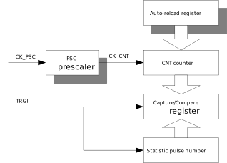
捕获定时器主要由计数器、预装载寄存器、预分频器以及捕获寄存器组成,框图如下所示。
功能描述
向上计数模式
该 Timer 是一个 16 位计数器,具有相关的自动重载寄存器。计数器以及自动重载寄存器都可以被软件读写。即使计数器正在运行,也可以进行读写操作。
时基单元包括:
计数器寄存器( TIMx_CNT )
自动重载寄存器( TIMx_ARR )
预分频器寄存器( TIMx_PSC )
Timer 工作在向上计数模式,计数器从 0 计数到自动重载值( TIMx_ARR 寄存器的内容)。当计数器达到自动重载值时,会产生计数器溢出事件。
统计脉冲宽度
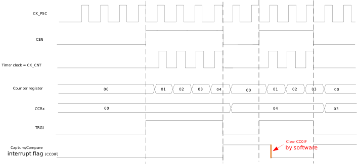
当 TIMx_CCR0 寄存器的 CC0PM 位设置为 0 时,捕获定时器则工作在捕获模式 0,该模式下可以统计 TRGI 有效电平的宽度。当 TRGI 从非有效电平转换到有效电平时,计数器自动使能。当 TRGI 从有效电平转换到非有效电平时,计数器自动禁用,CC0IF 被设置,并且当前计数值被复制到 TIMx_CCR0 寄存器的 CCR0 字段。
下图给出了统计脉冲宽度模式的一个示例,其中预分频器分频为 1,且 TRGI 的上升沿用于捕获。
统计脉冲数量
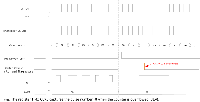
当 TIMx_CCR0 寄存器的 CC0PM 位设置为 1 时,捕获定时器则工作在捕获模式 1,该模式下可以统计给定周期内 TRGI 有效沿的数量。当计数器溢出时, CC0IF 被设置,并且该数量被复制到 TIMx_CCR0 寄存器的 CCR0 字段。
下图给出了统计脉冲数量模式的一个示例,其中预分频器分频为 1, TRGI 的上升沿用于捕获,且 ARR 字段等于 E6。
中断事件
捕获定时器的中断事件有两种类型:
向上计数模式下的中断事件可通过 TIMx_DIER 寄存器的 UIE 位配置使能。当 UIE 位为 1 时,若有中断事件发生,会触发系统中断。硬件溢出和软件触发更新,都会产生中断。对应中断状态可以通过 TIMx_SR 中的 UIF 查看,并可以通过写 UIF 清除对应中断。
捕获模式下的中断事件可通过 TIMx_DIER 寄存器的 CC0IE 位配置使能。捕获模式 0:当 TRGI 从有效电平转换到非有效电平时触发中断事件,并且当前计数值被复制到 TIMx_CCR0 寄存器的 CCR0 字段;捕获模式 1:当计数器溢出时触发中断事件,并且统计的脉冲数量的值被复制到 TIMx_CCR0 寄存器的 CCR0 字段。
PWM 定时器
简介
PWM 定时器由一个 16 位自动重载计数器和一个 16 位可编程预分频器驱动。它可用于多种目的,包括测量输入信号的脉冲频率(输入捕获)、单脉冲模式以及输出波形生成(PWM)。
特性
时钟源:XTAL40M
分辨率:16-bit
预分频器:16-bit
计数模式:向上计数
支持单脉冲模式
支持带极性选择的 PWM 模式
中断生成
睡眠模式
占空比范围:0 ~ 100%
支持移相功能
数量:
{{IC_PARAM_PWMTIMER_QUANTITY}}通道数:
{{IC_PARAM_PWMTIMER_CHANNEL_NUM}}
数量:
{{IC_PARAM_PWMTIMER_QUANTITY}}通道数:
{{IC_PARAM_PWMTIMER_CHANNEL_NUM}}
数量:
{{IC_PARAM_PWMTIMER_QUANTITY}}通道数:
{{IC_PARAM_PWMTIMER_CHANNEL_NUM}}
数量:
{{IC_PARAM_PWMTIMER_QUANTITY}}通道数:
{{IC_PARAM_PWMTIMER_CHANNEL_NUM}}
数量:
{{IC_PARAM_PWMTIMER_QUANTITY}}通道数:
{{IC_PARAM_PWMTIMER_CHANNEL_NUM}}
数量:
{{IC_PARAM_PWMTIMER_QUANTITY}}通道数:
{{IC_PARAM_PWMTIMER_CHANNEL_NUM}}
数量:
{{IC_PARAM_PWMTIMER_QUANTITY}}通道数:
{{IC_PARAM_PWMTIMER_CHANNEL_NUM}}
数量:
{{IC_PARAM_PWMTIMER_QUANTITY}}通道数:
{{IC_PARAM_PWMTIMER_CHANNEL_NUM}}
框图
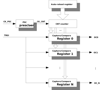
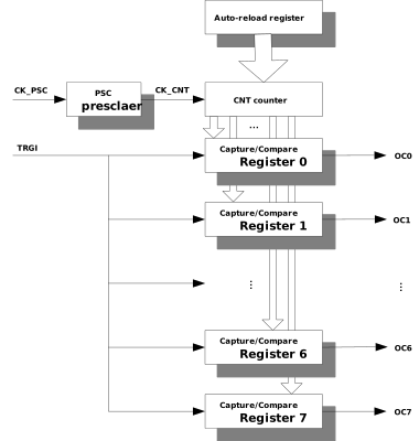
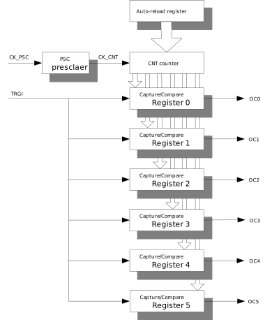
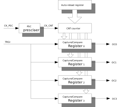
PWM 定时器主要由计数器、预装载寄存器、预分频器以及捕获/比较寄存器组成,同一 PWM 定时器的不同通道共用同一个计数器,不同通道可以输出不同的占空比和相位的波形,框图如下所示。
功能描述
向上计数模式
该 Timer 是一个 16 位计数器,具有相关的自动重载寄存器。计数器以及自动重载寄存器都可以被软件读写。即使计数器正在运行,也可以进行读写操作。
时基单元包括:
计数器寄存器( TIMx_CNT )
自动重载寄存器( TIMx_ARR )
预分频器寄存器( TIMx_PSC )
Timer 工作在向上计数模式,计数器从 0 计数到自动重载值( TIMx_ARR 寄存器的内容)。当计数器达到自动重载值时,会产生计数器溢出事件。
输入捕获模式
输入捕获模式允许定时器在外部触发信号的特定边沿到来时,自动锁存当前计数器的值。该功能可以应用于脉冲宽度测量、频率计算、信号周期检测等应用场景。
通过在 TIMx_CCRx 寄存器的 CCxM 位中写入 1 来使能输入捕获模式。使能后,捕获/比较寄存器 TIMx_CCRx 的 CCRx 字段将被用作捕获寄存器,用于锁存计数器的值,每个通道都有自己的捕获寄存器。
当检测到 TRGI 信号有效跳变沿时,定时器自动将当前计数器的值锁存到 TIMx_CCRx 寄存器中,不同通道可以配置成不同的极性,用于捕获 TRGI 信号不同边沿。同时,对应通道的 CCxIF 标志位在 TIMx_SR 状态寄存器中被置位。如果使能了相应的中断,系统将产生中断请求。
软件可以通过向 CCxIF 位写入 1 来清除该中断标志位。
单脉冲模式
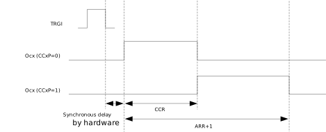
单脉冲模式 (OPM) 是 PWM 模式的一种特殊情况。它允许计数器响应刺激而启动,并在可编程延迟后产生一个可编程长度的脉冲。
启动计数器可以通过 TRGI 的有效边沿来控制,可以是上升沿、下降沿或双边沿。空闲状态下的默认输出电平可以配置成高或者低。产生波形可以在 PWM 模式下完成。您可以通过设置 TIMx_CR 寄存器中的 OPM 位来选择单脉冲模式。这将使计数器在下次更新时自动停止。
单脉冲模式的时序如下图所示。
备注
由于各个通道之间彼此独立,当 TRGI 用于触发一个或多个通道输出 PWM 信号时,它也可以在其他通道的输入捕获模式中用作捕获源。
PWM 模式
脉冲宽度调制模式允许您生成一个频率由寄存器的值确定、占空比由 TIMx_CCRx 寄存器中的 CCRx 字段的值确定的信号。
周期:TPWM = (ARR + 1) × TCNT
占空比:DPWM = (CCRx × TCNT) / TPWM
其中:TCNT = TXTAL × (PSC + 1)
通过在 TIMx_CCRx 寄存器中设置 OCxM 位为 0,可以在每个通道上独立选择 PWM 模式(每个 OCx 输出一个 PWM)。您必须通过设置 TIMx_CCRx 寄存器中的 OCxPE 位来启用相应的预装载寄存器,并最终通过设置 TIMx_CR 寄存器中的 ARPE 位来启用自动重载预装载寄存器。
由于预装载寄存器仅在更新事件发生时才传输到影子寄存器,因此在启动计数器之前,您必须通过设置 TIMx_EGR 寄存器中的 UG 位来初始化所有寄存器。
OCx 极性可以通过 TIMx_CCRx 寄存器中的 CCxP 位进行软件编程。它可以被编程为高电平有效或低电平有效。
在 PWM 模式下,TIMx_CNT 和 CCRx (在 TIMx_CCRx 中)总是被比较以确定是否 TIMx_CNT < CCRx。只要 TIMx_CNT < CCRx,PWM 信号 OCx 就保持有效,否则变为无效。如果 TIMx_CCRx 中的比较值大于 TIMx_ARR 中的自动重载值,则 PWM 信号 OCx 输出在整个周期内都有效。如果比较值为 0,则 PWM 信号 OCx 输出在整个周期内都无效。
该定时器仅能够在边对齐模式下生成 PWM。下图展示了一些边对齐 PWM 波形的示例,其中 TIMx_ARR = 8。
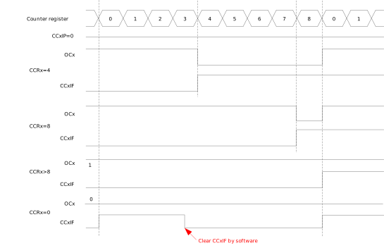
边对齐 PWM 波形(ARR = 8,CCxP = 0)
移相功能
此功能用于用户配置通道之间的特定相移。它仅适用于 PWM 模式和单脉冲模式,输入捕获模式不受影响。
备注
PWM 通道数量因芯片而异(参见特性章节)。本节以 6 个通道(通道 0 至 5)为例进行说明。
除 TIMx_CNT 寄存器中的 CNT 外,PWM 定时器为每个通道提供一个通道 Counter。通道 Counter 的值可以通过读取其 TIMx_PHASECNTx 寄存器获取(其中 x 为通道索引)。每个通道 Counter 的值是根据 TIMx_CNT 寄存器中的 CNT 值计算得出的。当 TIMx_CNT 中的 Counter 值发生变化时,通道值会立即更新。每个通道的波形以其自己的通道 Counter 作为基准。
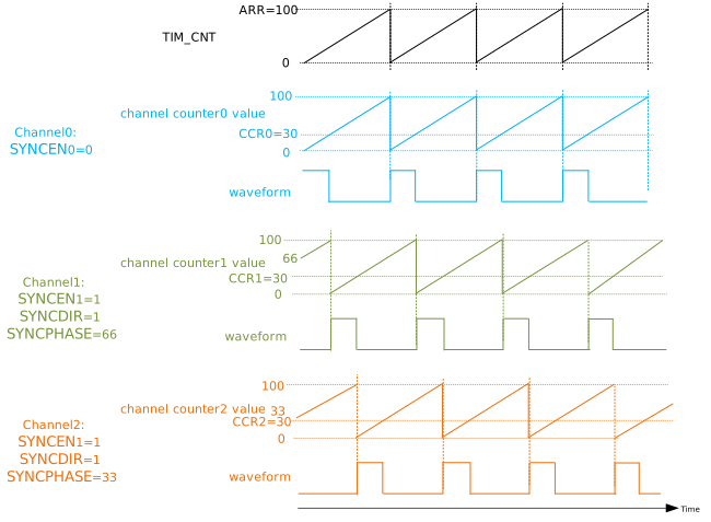
通道之间的相移是通过设置通道 Counter 相对于 TIMx_CNT 寄存器中的 CNT 值的相移来实现的。相移功能可以通过 TIMx_PSYNCx 寄存器进行配置(其中 x 为通道索引)。当通过设置 TIMx_PSYNCx 寄存器中的 SYNCENx 位来使能相移功能时,用户可以配置该通道 Counter 与 TIMx_CNT 中的 CNT 值之间的相移,相移值由 TIMx_PSYNCx 中的 SYNCDIR 和 SYNCPHASE 设置。当相移功能被禁用时,该通道的通道 Counter 值与 CNT 完全相同。通道 Counter 值为:
通道 Counter 值 = CNT - (-1)SYNCDIR* (SYNCPHASE)
硬件始终确保通道值在 0-ARR 范围内。当通道 Counter 值高于 ARR 时,它会立即变为 旧值 - ARR 以保持在 0-ARR 范围内;当通道 Counter 值低于零时,它会立即变为 旧值 + ARR。
相移功能 展示了通道 Counter 值相对于 Counter 的变化曲线,以及从通道 0、1、2 的通道 Counter 生成的相应波形。在以下配置中,每两个通道之间的相移为 1/3。
在上述示例中,对于通道 0,通道 0 的 SYNCEN0 为 0,因此通道 counter0 始终等于 CNT。当通道 counter0 低于 CCR0*(即 30)时,通道 0 输出高电平;当通道 *counter0 高于 CCR0 时,通道 0 输出低电平。对于通道 1,SYNCEN1 被设置为 1,因此通道 counter1 与 TIMx_CNT 存在相移。通道 Counter 1 的值为 CNT + 66,其中 CNT 是 TIMx_CNT 的值。当通道 counter1 低于 CCR1 时,通道 1 输出高电平,反之亦然。对于通道 2,通道 counter2 为 CNT + 33。在上述设置下,每两个通道之间存在 1/3 的相移。
软件确保 SYNCPHASEx 始终小于 ARR 值。否则,将生成并输出低电平。
PWM 定时器使能并生成波形后,用户可能需要更新一些参数,如周期、占空比和相移值。由于 ARR、PSC、CCRx 和 PSYNCx 寄存器可以配置为预装载或非预装载,用户有三种方式可以在运行时更改配置。
将寄存器设置为非预装载,然后设置新值,新值将在寄存器值更改后立即生效。
将寄存器设置为预装载,然后设置新值,新值将在 CNT 的下一次 UEV 后更新。
将寄存器设置为预装载,设置新值,然后写入 UG 位,之后 CNT 将清零并从 0 开始重新计数,新值将立即生效。这有助于在需要立即更新多个参数时使用。
相移功能
以下小节说明了一些情况。
立即更新
修改周期
增加 ARR 值
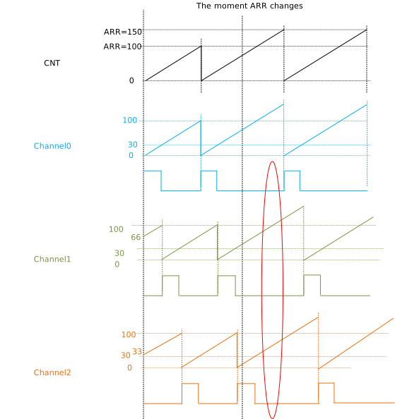
ARR 从 100 改变为 150 时的波形 说明了当 ARR 值从 100 改变为 150 时的情况。由于 ARR 值增加了,红色周期中的波形显示所有三个通道都处于低电平状态。
减小 ARR 值
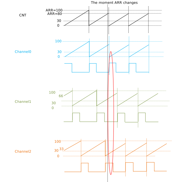
ARR 从 100 改变为 80 时的波形 展示了当 ARR 值从 100 改变为 80 时的情况。在 ARR 值减小之前,同一时间只有一个通道处于高电平状态。当 ARR 被设置为 80 后,红色周期中的波形显示在这种情况下通道 0 和通道 2 都处于高电平状态。
ARR 从 100 改变为 150 时的波形
ARR 从 100 改变为 80 时的波形
修改占空比
每个通道的占空比取决于其 CCRx 值,该值在各自的 TIMx_CCRx 寄存器中单独配置。由于 CPU 执行指令时存在时间间隔,它们无法完全在同一时刻更新。该时间间隔的长度是不可预测的。以下示例忽略了这个时间间隔。
增加 CCRx 值
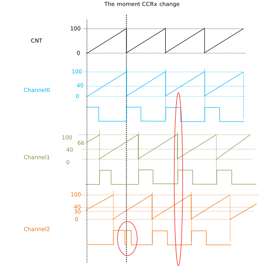
下图展示了当 CCRx 从 30 改变为 40 时的情况。对于通道 2,CCR2 在通道 counter2 值为 35 时被改变,并且
30 < 35 < 40,因此通道 2 的波形在 CCRx 更新时同时变为高电平。这会导致毛刺产生。此外,在这种情况下,通道 0 和通道 1 由于其 CCRx 值增加而都处于高电平状态。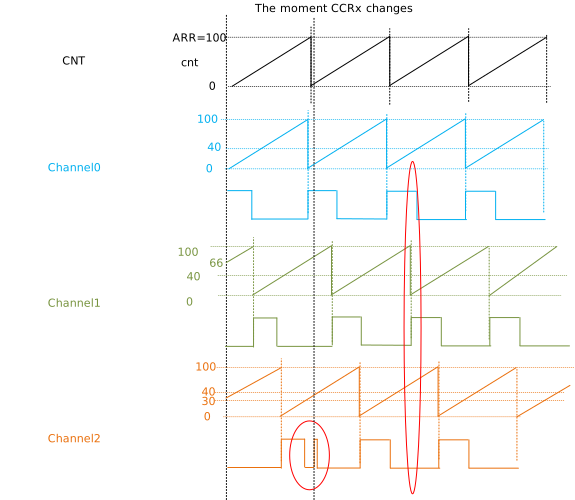
减小 CCRx 值
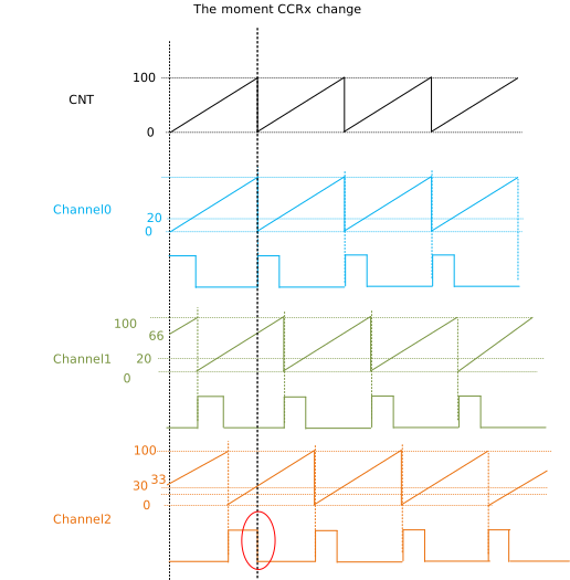
下图展示了当 CCRx 从 30 改变为 20 时的情况。对于通道 2,CCR2 在通道 counter2 值为 25 时被改变,并且
20 < 25 < 30,因此通道 2 的波形在 CCRx 更新时同时变为低电平。在这个周期中,通道 2 的占空比既不是 20% 也不是 30%,而是 25%。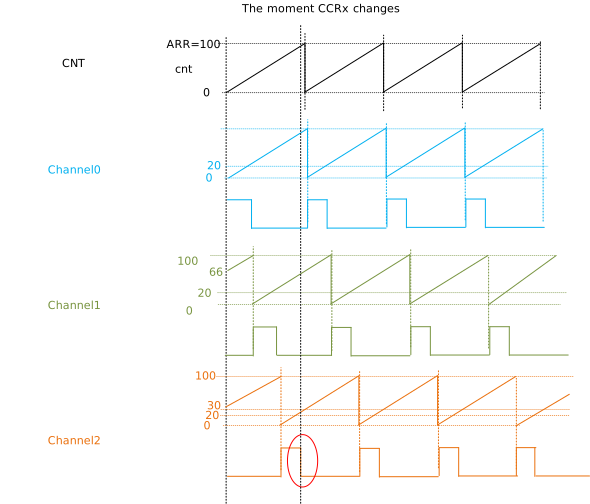
修改相移值
每个通道的相移在 TIMx_PSYNCx 寄存器中单独配置。它们无法完全在同一时刻更新,以下示例忽略了这个时间间隔。此外,相移的改变总是会导致各通道计数器和波形的不连续。下图是一个示例,通道 1 的相移从 66 改变为 36,通道 2 从 33 改变为 63。对于通道 1,通道 counter1 在改变前后分别高于和低于 CCR1。对于通道 2,通道 counter2 在改变前后分别低于和高于 CCR2。
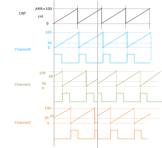
相移改变时的波形
在 CNT 的下一次 UEV 后更新
更改周期
增加 ARR 值
ARR 从 100 变更为 150 时的波形 说明了当 ARR 值从 100 变更为 150 时的情况。由于 ARR 增大,红色周期中的波形显示在此情况下所有三个通道都处于低电平状态。
减小 ARR 值
ARR 从 100 变更为 80 时的波形 展示了当 ARR 值从 100 变更为 80 时的情况。在 ARR 减小之前,同一时间只有一个通道处于高电平状态;在 ARR 设置为 80 后,红色周期中的波形显示在此情况下通道 0 和 2 都处于高电平状态。
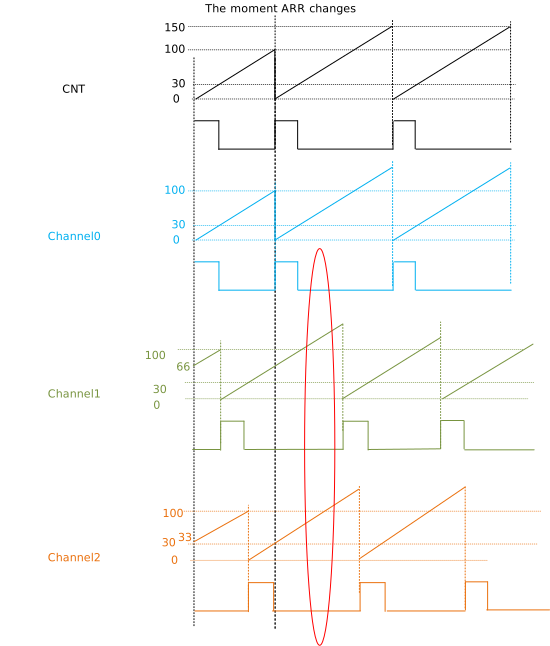
ARR 从 100 变更为 150 时的波形
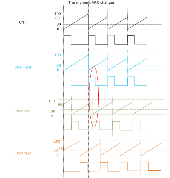
ARR 从 100 变更为 80 时的波形
更改占空比
以下示例忽略配置的时间间隔。波形与 CCRx 立即更新的情况类似。
增加 CCRx 值
下图展示了 CCRx 从 30 变更为 40 时的情况。
减小 CCRx 值
下图展示了 CCRx 从 30 变更为 20 时的情况。
更改相移值
以下示例忽略配置的时间间隔;波形与相移立即更新的情况类似。
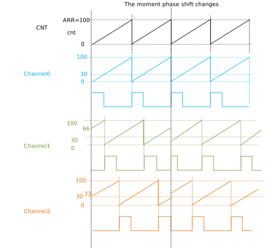
相移变化时的波形
在写入 UG 位后更新
在写入 UG 位之前,波形是根据旧配置生成的。新配置在写入 UG 位后生效,同时 CNT 和通道计数器被清零。在下面的例子中,ARR 从 100 变为 150,CCRx 保持不变,通道 0 的相移功能被禁用,通道 1 的相移从 66 变为 33,通道 2 的相移从 33 变为 66。
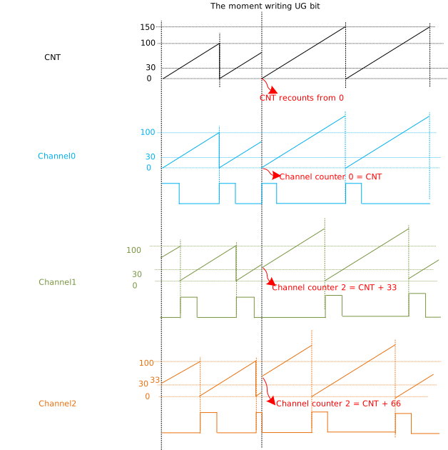
写入 UG 位时的波形
寄存器
捕获定时器寄存器
Base Address: 0x41100200
Name |
Address offset |
Access |
Description |
|---|---|---|---|
000h |
R/W |
Users can configure and observe the counter operation. |
|
004h |
R/W |
This register is about the update operation. |
|
008h |
R/W |
||
00Ch |
R/W |
||
010h |
R/W |
This register is about the update operation, and is user-defined. |
|
014h |
R |
This is timer count register. |
|
018h |
R/W |
This is prescaler value register. |
|
01Ch |
R/W |
This is auto-reload value register. |
|
024h |
R/W |
This is the register about input capture configuration and the data of capture. |
|
028h |
R/W |
||
02Ch |
R/W |
REG_TIM_EN
Name: TIM enable register
Size: 32
Address offset: 000h
Read/write access: R/W
Users can configure and observe the counter operation.
Bit |
Symbol |
Access |
INI |
Description |
|---|---|---|---|---|
31:17 |
RSVD |
R |
- |
Reserved |
16 |
CNT_EN |
R |
0x0 |
Counter working status
|
15:9 |
RSVD |
R |
- |
Reserved |
8 |
CEN |
R |
0x0 |
Counter run status
|
7:2 |
RSVD |
R |
- |
Reserved |
1 |
CNT_STOP |
R/W |
0x0 |
Disable the counter Poll CNT_RUN to see the counter status. If CNT_RUN is 0, it means that the counter has been disabled internally. |
0 |
CNT_START |
R/W |
0x0 |
Enable the counter Poll CNT_RUN to see the counter status. If CNT_RUN is 1, it means that the counter has been enabled internally. |
REG_TIM_CR
Name: TIM control register
Size: 32
Address offset: 004h
Read/write access: R/W
This register is about the update operation.
Bit |
Symbol |
Access |
INI |
Description |
|---|---|---|---|---|
31:5 |
RSVD |
R |
- |
Reserved |
4 |
ARPE |
R/W |
0x0 |
Enable auto-reload preloading
|
3 |
RSVD |
R |
- |
Reserved |
2 |
URS |
R/W |
0x0 |
Update request source
|
1 |
UDIS |
R/W |
0x0 |
Disable UEV Shadow registers keep their values. Otherwise, buffered registers are then loaded with their preload values when UEV happens. |
0 |
RSVD |
R |
- |
Reserved |
REG_TIM_DIER
Name: TIM interrupt enable register
Size: 32
Address offset: 008h
Read/write access: R/W
Bit |
Symbol |
Access |
INI |
Description |
|---|---|---|---|---|
31:2 |
RSVD |
R |
- |
Reserved |
1 |
CC0IE |
R/W |
0x0 |
Enable Capture/Compare 0 interrupt |
0 |
UIE |
R/W |
0x0 |
Enable update interrupt |
REG_TIM_SR
Name: TIM status register
Size: 32
Address offset: 00Ch
Read/write access: R/W
Bit |
Symbol |
Access |
INI |
Description |
|---|---|---|---|---|
31 |
UG_DONE |
R |
0x1 |
UG operation status This bit is cleared by hardware when the UG bit in the TIMx_EGR register is set. When the UG operation is done, hardware set this bit to '1'. So, software can poll this bit to see the UG operation status. |
30:2 |
RSVD |
R |
- |
Reserved |
1 |
CC0IF |
R/W |
0x0 |
Capture/Compare 0 interrupt flag CC0 channel configured as pulse mode 0: This bit is set when TRGI is transferred to inactive level from active level. CC0 channel configured as pulse mode 1: This bit is set by hardware when the counter overflows. It is cleared by software. |
0 |
UIF |
R/W |
0x0 |
Update interrupt flag |
REG_TIM_EGR
Name: TIM event generation register
Size: 32
Address offset: 010h
Read/write access: R/W
This register is about the update operation, and is user-defined.
Bit |
Symbol |
Access |
INI |
Description |
|---|---|---|---|---|
31:2 |
RSVD |
R |
- |
Reserved |
1 |
CC0G |
R/W |
0x0 |
Capture/Compare 0 generation This bit is set by software and is automatically cleared by hardware. A Capture/Compare event is generated on channel 0: the current value of the counter is captured in TIM_CCR0 register. The CC0IF flag is set, the corresponding interrupt or request is sent if enabled. |
0 |
UG |
R/W |
0x0 |
Update generation Re-initialize the counter and generate an update of registers. Note that the prescaler counter is cleared too. (anyway the prescaler ratio is not affected) |
REG_TIM_CNT
Name: TIM counter
Size: 32
Address offset: 014h
Read/write access: R
This is timer count register.
Bit |
Symbol |
Access |
INI |
Description |
|---|---|---|---|---|
31:16 |
RSVD |
R |
- |
Reserved |
15:0 |
CNT |
R |
0x0 |
Counter value |
REG_TIM_PSC
Name: TIM prescaler register
Size: 32
Address offset: 018h
Read/write access: R/W
This is prescaler value register.
Bit |
Symbol |
Access |
INI |
Description |
|---|---|---|---|---|
31:16 |
RSVD |
R |
- |
Reserved |
15:0 |
PSC |
R/W |
0x0 |
Prescaler value PSC contains the value to be loaded in the actual prescaler register at each UEV (including when the counter is cleared through UG bit of TIM_EGR register). |
REG_TIM_ARR
Name: TIM auto-reload register
Size: 32
Address offset: 01Ch
Read/write access: R/W
This is auto-reload value register.
Bit |
Symbol |
Access |
INI |
Description |
|---|---|---|---|---|
31:16 |
RSVD |
R |
- |
Reserved |
15:0 |
ARR |
R/W |
0xFFFF |
The value to be loaded in the actual auto-reload register. It can be preloaded by setting ARPE bit in TIM_CR. |
REG_TIM_CCR0
Name: TIM Capture register
Size: 32
Address offset: 024h
Read/write access: R/W
This is the register about input capture configuration and the data of capture.
Bit |
Symbol |
Access |
INI |
Description |
|---|---|---|---|---|
31:29 |
RSVD |
R |
- |
Reserved |
28 |
CC0PM |
R/W |
0x0 |
CC0 pulse mode
|
27 |
RSVD |
R |
- |
Reserved |
26 |
CC0P |
R/W |
0x0 |
CC0 channel configured as output:
CC0 channel configured as input:
|
25 |
RSVD |
R |
- |
Reserved |
24 |
CC0E |
R/W |
0x0 |
Enable CC0 |
23:16 |
RSVD |
R |
- |
Reserved |
15:0 |
CCR0 |
R/W |
0x0 |
Capture/Compare 0 value CC0 channel configured as pulse mode 0: the pulse width of TRGI CC0 channel configured as pulse mode 1: the pulse number of TRGI when the counter counts from 0 to ARR |
REG_TIM_PULSE_DBC
Name: Timer Pulse DBC Register
Size: 32
Address offset: 028h
Read/write access: R/W
Bit |
Symbol |
Access |
INI |
Description |
|---|---|---|---|---|
31:16 |
RSVD |
R |
- |
Reserved |
15:1 |
R_DBC_CYC |
R/W |
0x0 |
DBC cycle |
0 |
R_DBC_FEN |
R/W |
0x0 |
Enable debounce for pulse
|
REG_TIM_PULSE_DUMMY
Name: Timer Pulse Dummy Register
Size: 32
Address offset: 02Ch
Read/write access: R/W
Bit |
Symbol |
Access |
INI |
Description |
|---|---|---|---|---|
31:0 |
DUMMY |
R/W |
ffffh |
Dummy register |
Base Address: 0x41019200
Name |
Address offset |
Access |
Description |
|---|---|---|---|
000h |
R/W |
User can configure and observe the counter operation. |
|
004h |
R/W |
This is the register about the update operation. |
|
008h |
R/W |
||
00Ch |
R/W |
This is the register about timer status. |
|
010h |
R/W |
Update generation, user defined |
|
014h |
R |
||
018h |
R/W |
||
01Ch |
R/W |
||
024h |
R/W |
This is the register about input capture configuration and the data of capture. |
|
028h |
R/W |
REG_TIM_EN
Name: TIM enable register
Size: 32
Address offset: 000h
Read/write access: R/W
User can configure and observe the counter operation.
Bit |
Symbol |
Access |
INI |
Description |
|---|---|---|---|---|
31:17 |
RSVD |
R |
- |
Reserved |
16 |
CNT_EN |
R |
0x0 |
Counter working status
|
15:9 |
RSVD |
R |
- |
Reserved |
8 |
CEN |
R |
0x0 |
Counter run status
|
7:2 |
RSVD |
R |
- |
Reserved |
1 |
CNT_STOP |
R/W |
0x0 |
Disable the counter. Poll CNT_RUN to see the counter status. If CNT_RUN is 0, it means that the counter has been disabled internally. |
0 |
CNT_START |
R/W |
0x0 |
Enable the counter. Poll CNT_RUN to see the counter status. If CNT_RUN is 1, it means that the counter has been enabled internally. |
REG_TIM_CR
Name: TIM control register
Size: 32
Address offset: 004h
Read/write access: R/W
This is the register about the update operation.
Bit |
Symbol |
Access |
INI |
Description |
|---|---|---|---|---|
31:5 |
RSVD |
R |
- |
Reserved |
4 |
ARPE |
R/W |
0x0 |
Enable auto-reload preloading
|
3 |
RSVD |
R |
- |
Reserved |
2 |
URS |
R/W |
0x0 |
Update request source
|
1 |
UDIS |
R/W |
0x0 |
Disable UEV Shadow registers keep their values. Otherwise, buffered registers are then loaded with their preload values when UEV happens. |
0 |
RSVD |
R |
- |
Reserved |
REG_TIM_DIER
Name: TIM interupt enable register
Size: 32
Address offset: 008h
Read/write access: R/W
Bit |
Symbol |
Access |
INI |
Description |
|---|---|---|---|---|
31:2 |
RSVD |
R |
- |
Reserved |
1 |
CC0IE |
R/W |
0x0 |
Enable Capture/Compare 0 interrupt |
0 |
UIE |
R/W |
0x0 |
Enable update interrupt |
REG_TIM_SR
Name: TIM status register
Size: 32
Address offset: 00Ch
Read/write access: R/W
This is the register about timer status.
Bit |
Symbol |
Access |
INI |
Description |
|---|---|---|---|---|
31 |
UG_DONE |
R |
0x1 |
UG operation status This bit is cleared by hardware when the UG bit in the TIMx_EGR register is set. When the UG operation is done, hardware sets this bit to '1'. So, software can poll this bit to see the UG operation status. |
30:2 |
RSVD |
R |
- |
Reserved |
1 |
CC0IF |
R/W |
0x0 |
Capture/Compare 0 interrupt flag
|
0 |
UIF |
R/W |
0x0 |
Update interrupt flag |
REG_TIM_EGR
Name: TIM event generation register
Size: 32
Address offset: 010h
Read/write access: R/W
Update generation, user defined
Bit |
Symbol |
Access |
INI |
Description |
|---|---|---|---|---|
31:2 |
RSVD |
R |
- |
Reserved |
1 |
CC0G |
R/W |
0x0 |
Capture/Compare 0 generation This bit is set by software and is automatically cleared by hardware. A Capture/Compare event is generated on channel 0: the current value of the counter is captured in TIM_CCR0 register. The CC0IF flag is set, the corresponding interrupt or request is sent if enabled. |
0 |
UG |
R/W |
0x0 |
Update generation. Re-initialize the counter and generate an update of registers. Note that the prescaler counter is cleared too. (Anyway the prescaler ratio is not affected) |
REG_TIM_CNT
Name: TIM counter register
Size: 32
Address offset: 014h
Read/write access: R
Bit |
Symbol |
Access |
INI |
Description |
|---|---|---|---|---|
31:16 |
RSVD |
R |
- |
Reserved |
15:0 |
CNT |
R |
0x0 |
Counter value |
REG_TIM_PSC
Name: TIM prescaler register
Size: 32
Address offset: 018h
Read/write access: R/W
Bit |
Symbol |
Access |
INI |
Description |
|---|---|---|---|---|
31:16 |
RSVD |
R |
- |
Reserved |
15:0 |
PSC |
R/W |
0x0 |
Prescaler value PSC contains the value to be loaded in the actual prescaler register at each UEV (including when the counter is cleared through UG bit of TIM_EGR register). |
REG_TIM_ARR
Name: TIM auto-reload register
Size: 32
Address offset: 01Ch
Read/write access: R/W
Bit |
Symbol |
Access |
INI |
Description |
|---|---|---|---|---|
31:16 |
RSVD |
R |
- |
Reserved |
15:0 |
ARR |
R/W |
0xFFFF |
The value to be loaded in the actual auto-reload register. It can be preloaded by setting ARPE bit in TIM_CR. |
REG_TIM_CCR0
Name: TIM Capture register
Size: 32
Address offset: 024h
Read/write access: R/W
This is the register about input capture configuration and the data of capture.
Bit |
Symbol |
Access |
INI |
Description |
|---|---|---|---|---|
31:29 |
RSVD |
R |
- |
Reserved |
28 |
CC0PM |
R/W |
0x0 |
CC0 pulse mode
|
27 |
RSVD |
R |
- |
Reserved |
26 |
CC0P |
R/W |
0x0 |
CC0 channel configured as output:
CC0 channel configured as input:
|
25 |
RSVD |
R |
- |
Reserved |
24 |
CC0E |
R/W |
0x0 |
Enable CC0 |
23:16 |
RSVD |
R |
- |
Reserved |
15:0 |
CCR0 |
R/W |
0x0 |
Capture/Compare 0 value CC0 channel configured as pulse mode 0: the pulse width of TRGI CC0 channel configured as pulse mode 1: the pulse number of TRGI when the counter counts from 0 to ARR |
REG_TIM_PULSE_DUMMY
Name: Timer Pulse Dummy Register
Size: 32
Address offset: 028h
Read/write access: R/W
Bit |
Symbol |
Access |
INI |
Description |
|---|---|---|---|---|
31:0 |
DUMMY |
R/W |
ffffh |
Dummy register |
REGISTER_CONTENTS=RTL8720E
REGISTER_CONTENTS=RTL8720E
REGISTER_CONTENTS=RTL8720E
Base Address: 0x4100A200
Name |
Address offset |
Access |
Description |
|---|---|---|---|
000h |
R/W |
||
004h |
R/W |
||
008h |
R/W |
||
00Ch |
R/W |
||
010h |
R/W |
||
014h |
R |
||
018h |
R/W |
||
01Ch |
R/W |
||
024h |
R/W |
REG_TIM_EN
Name: TIM enable register
Size: 32
Address offset: 000h
Read/write access: R/W
Bit |
Symbol |
Access |
INI |
Description |
|---|---|---|---|---|
31:17 |
RSVD |
R |
- |
Reserved |
16 |
CNT_EN |
R |
0x0 |
Counter working status
|
15:9 |
RSVD |
R |
- |
Reserved |
8 |
CEN |
R |
0x0 |
Counter run status
|
7:2 |
RSVD |
R |
- |
Reserved |
1 |
CNT_STOP |
R/W |
0x0 |
Disable the counter. Poll CNT_RUN to see the counter status. If CNT_RUN is 0, it means that the counter has been disabled internally. |
0 |
CNT_START |
R/W |
0x0 |
Enable the counter. Poll CNT_RUN to see the counter status. If CNT_RUN is 1, it means that the counter has been enabled internally. |
REG_TIM_CR
Name: TIM control register
Size: 32
Address offset: 004h
Read/write access: R/W
Bit |
Symbol |
Access |
INI |
Description |
|---|---|---|---|---|
31:5 |
RSVD |
R |
- |
Reserved |
4 |
ARPE |
R/W |
0x0 |
Enable auto-reload preloading
|
3 |
RSVD |
R |
- |
Reserved |
2 |
URS |
R/W |
0x0 |
Update request source
|
1 |
UDIS |
R/W |
0x0 |
Disable UEV. Shadow registers keep their values. Otherwise, buffered registers are then loaded with their preload values when UEV happen. |
0 |
RSVD |
R |
- |
Reserved |
REG_TIM_DIER
Name: TIM interupt enable register
Size: 32
Address offset: 008h
Read/write access: R/W
Bit |
Symbol |
Access |
INI |
Description |
|---|---|---|---|---|
31:2 |
RSVD |
R |
- |
Reserved |
1 |
CC0IE |
R/W |
0x0 |
Enable capture/compare 0 interrupt |
0 |
UIE |
R/W |
0x0 |
Enable update interrupt |
REG_TIM_SR
Name: TIM status register
Size: 32
Address offset: 00Ch
Read/write access: R/W
Bit |
Symbol |
Access |
INI |
Description |
|---|---|---|---|---|
31 |
UG_DONE |
R |
0x1 |
UG operation status.This bit is cleared by hardware when the UG bit in the timx_EGR register is set. When the UG operation is done, hardware set this bit to '1'. So, software can poll this bit to see the UG operation status. |
30:2 |
RSVD |
R |
- |
Reserved |
1 |
CC0IF |
R/W |
0x0 |
Capture/compare 0 interrupt flag Cc0 channel configured as pulse mode 0: This bit is set when trgi is transferred to inactive level from active level. Cc0 channel configured as pulse mode 1: This bit is set by hardware when the counter overflows. it is cleared by software. |
0 |
UIF |
R/W |
0x0 |
Update interrupt flag |
REG_TIM_EGR
Name: TIM event generation register
Size: 32
Address offset: 010h
Read/write access: R/W
Bit |
Symbol |
Access |
INI |
Description |
|---|---|---|---|---|
31:2 |
RSVD |
R |
- |
Reserved |
1 |
CC0G |
R/W |
0x0 |
Capture/Compare 0 generation. This bit is set by software and is automatically cleared by hardware. A Capture/Compare event is generated on channel 0: the current value of the counter is captured in TIM_CCR0 register. The CC0IF flag is set, the corresponding interrupt or request is sent if enabled. |
0 |
UG |
R/W |
0x0 |
Update generation. Re-initialize the counter and generate an update of registers. Note that the prescaler counter is cleared too.(anyway the prescaler ratio is not affected) |
REG_TIM_CNT
Name: TIM counter
Size: 32
Address offset: 014h
Read/write access: R
Bit |
Symbol |
Access |
INI |
Description |
|---|---|---|---|---|
31:16 |
RSVD |
R |
- |
Reserved |
15:0 |
CNT |
R |
0x0 |
Counter value |
REG_TIM_PSC
Name: TIM prescaler register
Size: 32
Address offset: 018h
Read/write access: R/W
Bit |
Symbol |
Access |
INI |
Description |
|---|---|---|---|---|
31:16 |
RSVD |
R |
- |
Reserved |
15:0 |
PSC |
R/W |
0x0 |
Prescaler value. psc contains the value to be loaded in the actual prescaler register at each uev(including when the counter is cleared through ug bit of tim_egr register). |
REG_TIM_ARR
Name: TIM auto-reload register
Size: 32
Address offset: 01Ch
Read/write access: R/W
Bit |
Symbol |
Access |
INI |
Description |
|---|---|---|---|---|
31:16 |
RSVD |
R |
- |
Reserved |
15:0 |
ARR |
R/W |
0xFFFF |
The value to be loaded in the actual auto-reload register. it can be preloaded by setting arpe bit in tim_cr. |
REG_TIM_CCR0
Name: TIM Capture register
Size: 32
Address offset: 024h
Read/write access: R/W
Bit |
Symbol |
Access |
INI |
Description |
|---|---|---|---|---|
31:29 |
RSVD |
R |
- |
Reserved |
28 |
CC0PM |
R/W |
0x0 |
CC0 pulse mode
|
27 |
RSVD |
R |
- |
Reserved |
26 |
CC0P |
R/W |
0x0 |
CC0 channel configured as output:
CC0 channel configured as input:
|
25 |
RSVD |
R |
- |
Reserved |
24 |
CC0E |
R/W |
0x0 |
Enable cc0 |
23:16 |
RSVD |
R |
- |
Reserved |
15:0 |
CCR0 |
R/W |
0x0 |
Capture/compare 0 value Cc0 channel configured as pulse mode 0: the pulse width of trgi Cc0 channel configured as pulse mode 1: the pulse number of trgi when the counter counts from 0 to arr |
Base Address: 0x41000800
Name |
Address offset |
Access |
Description |
|---|---|---|---|
000h |
R/W |
User can configure and observe the counter operation |
|
004h |
R/W |
Registers about the update operation |
|
008h |
R/W |
Interrupt enable |
|
00Ch |
R/W |
Registers about timer status |
|
010h |
R/W |
Update generation user defined |
|
014h |
R |
Timer count |
|
018h |
R/W |
Prescaler value |
|
01Ch |
R/W |
Auto-reload value |
|
024h |
R/W |
Input capture configuration and the data of capture |
|
028h |
R/W |
||
02Ch |
R/W |
Dummy register |
REG_TIM_EN
Name: TIM enable register
Size: 32
Address offset: 000h
Read/write access: R/W
User can configure and observe the counter operation
Bit |
Symbol |
Access |
INI |
Description |
|---|---|---|---|---|
31:17 |
RSVD |
R |
- |
Reserved |
16 |
CNT_EN |
R |
0x0 |
Counter working status
|
15:9 |
RSVD |
R |
- |
Reserved |
8 |
CEN |
R |
0x0 |
Counter run status
|
7:2 |
RSVD |
R |
- |
Reserved |
1 |
CNT_STOP |
R/W |
0x0 |
Disable the counter. Poll CNT_RUN to see the counter status. If CNT_RUN is 0, it means that the counter has been disabled internally. |
0 |
CNT_START |
R/W |
0x0 |
Enable the counter. Poll CNT_RUN to see the counter status. If CNT_RUN is 1, it means that the counter has been enabled internally. |
REG_TIM_CR
Name: TIM control register
Size: 32
Address offset: 004h
Read/write access: R/W
Registers about the update operation
Bit |
Symbol |
Access |
INI |
Description |
|---|---|---|---|---|
31:5 |
RSVD |
R |
- |
Reserved |
4 |
ARPE |
R/W |
0x0 |
Enable auto-reload preloading
|
3 |
RSVD |
R |
- |
Reserved |
2 |
URS |
R/W |
0x0 |
Update request source
|
1 |
UDIS |
R/W |
0x0 |
Disable UEV. Shadow registers keep their values. Otherwise, buffered registers are then loaded with their preload values when UEV happen. |
0 |
RSVD |
R |
- |
Reserved |
REG_TIM_DIER
Name: TIM interupt enable register
Size: 32
Address offset: 008h
Read/write access: R/W
Interrupt enable
Bit |
Symbol |
Access |
INI |
Description |
|---|---|---|---|---|
31:2 |
RSVD |
R |
- |
Reserved |
1 |
CC0IE |
R/W |
0x0 |
Enable Capture/Compare 0 interrupt |
0 |
UIE |
R/W |
0x0 |
Enable update interrupt |
REG_TIM_SR
Name: TIM status register
Size: 32
Address offset: 00Ch
Read/write access: R/W
Registers about timer status
Bit |
Symbol |
Access |
INI |
Description |
|---|---|---|---|---|
31 |
UG_DONE |
R |
0x1 |
UG operation status This bit is cleared by hardware when the UG bit in the TIMx_EGR register is set. When the UG operation is done, hardware set this bit to '1'. So, software can poll this bit to see the UG operation status. |
30:2 |
RSVD |
R |
- |
Reserved |
1 |
CC0IF |
R/W |
0x0 |
Capture/Compare 0 interrupt flag CC0 channel configured as pulse mode 0: This bit is set when TRGI is transferred to inactive level from active level. CC0 channel configured as pulse mode 1: This bit is set by hardware when the counter overflows. It is cleared by software. |
0 |
UIF |
R/W |
0x0 |
Update interrupt flag |
REG_TIM_EGR
Name: TIM event generation register
Size: 32
Address offset: 010h
Read/write access: R/W
Update generation user defined
Bit |
Symbol |
Access |
INI |
Description |
|---|---|---|---|---|
31:2 |
RSVD |
R |
- |
Reserved |
1 |
CC0G |
R/W |
0x0 |
Capture/Compare 0 generation. This bit is set by software and is automatically cleared by hardware. A Capture/Compare event is generated on channel 0: the current value of the counter is captured in TIM_CCR0 register. The CC0IF flag is set, the corresponding interrupt or request is sent if enabled. |
0 |
UG |
R/W |
0x0 |
Update generation. Re-initialize the counter and generate an update of registers. Note that the prescaler counter is cleared too.(anyway the prescaler ratio is not affected) |
REG_TIM_CNT
Name: TIM counter
Size: 32
Address offset: 014h
Read/write access: R
Timer count
Bit |
Symbol |
Access |
INI |
Description |
|---|---|---|---|---|
31:16 |
RSVD |
R |
- |
Reserved |
15:0 |
CNT |
R |
0x0 |
Counter value |
REG_TIM_PSC
Name: TIM prescaler register
Size: 32
Address offset: 018h
Read/write access: R/W
Prescaler value
Bit |
Symbol |
Access |
INI |
Description |
|---|---|---|---|---|
31:16 |
RSVD |
R |
- |
Reserved |
15:0 |
PSC |
R/W |
0x0 |
Prescaler value. PSC contains the value to be loaded in the actual prescaler register at each UEV(including when the counter is cleared through UG bit of TIM_EGR register). |
REG_TIM_ARR
Name: TIM auto-reload register
Size: 32
Address offset: 01Ch
Read/write access: R/W
Auto-reload value
Bit |
Symbol |
Access |
INI |
Description |
|---|---|---|---|---|
31:16 |
RSVD |
R |
- |
Reserved |
15:0 |
ARR |
R/W |
0xFFFF |
The value to be loaded in the actual auto-reload register. It can be preloaded by setting ARPE bit in TIM_CR. |
REG_TIM_CCR0
Name: TIM Capture register
Size: 32
Address offset: 024h
Read/write access: R/W
Input capture configuration and the data of capture
Bit |
Symbol |
Access |
INI |
Description |
|---|---|---|---|---|
31:29 |
RSVD |
R |
- |
Reserved |
28 |
CC0PM |
R/W |
0x0 |
CC0 pulse mode
|
27 |
RSVD |
R |
- |
Reserved |
26 |
CC0P |
R/W |
0x0 |
CC0 channel configured as output:
CC0 channel configured as input:
|
25 |
RSVD |
R |
- |
Reserved |
24 |
CC0E |
R/W |
0x0 |
Enable CC0 |
23:16 |
RSVD |
R |
- |
Reserved |
15:0 |
CCR0 |
R/W |
0x0 |
Capture/Compare 0 value CC0 channel configured as pulse mode 0: the pulse width of TRGI CC0 channel configured as pulse mode 1: the pulse number of TRGI when the counter counts from 0 to ARR |
REG_TIM_PULSE_DBC
Name: Timer Pulse dbc Register
Size: 32
Address offset: 028h
Read/write access: R/W
Bit |
Symbol |
Access |
INI |
Description |
|---|---|---|---|---|
31:16 |
RSVD |
R |
- |
Reserved |
15:1 |
R_DBC_CYC |
R/W |
0x0 |
Dbc cycle |
0 |
R_DBC_FEN |
R/W |
0x0 |
Enable debounce for pluse
|
REG_TIM_PULSE_DUMMY
Name: Timer Pulse Dummy Register
Size: 32
Address offset: 02Ch
Read/write access: R/W
Dummy register
Bit |
Symbol |
Access |
INI |
Description |
|---|---|---|---|---|
31:0 |
DUMMY |
R/W |
ffffh |
Dummy register |
Base Address: 0x401C7400
Name |
Address offset |
Access |
Description |
|---|---|---|---|
000h |
R/W |
User can configure and observe the counter operation |
|
004h |
R/W |
Registers about the update operation |
|
008h |
R/W |
Interrupt enable |
|
00Ch |
R/W |
Registers about timer status |
|
010h |
R/W |
Update generation user defined |
|
014h |
R |
Timer count |
|
018h |
R/W |
Prescaler value |
|
01Ch |
R/W |
Auto-reload value |
|
024h |
R/W |
Input capture configuration and the data of capture |
|
028h |
R/W |
||
02Ch |
R/W |
Dummy register |
REG_TIM_EN
Name: TIM enable register
Size: 32
Address offset: 000h
Read/write access: R/W
User can configure and observe the counter operation
Bit |
Symbol |
Access |
INI |
Description |
|---|---|---|---|---|
31:17 |
RSVD |
R |
- |
Reserved |
16 |
CNT_EN |
R |
0x0 |
Counter working status
|
15:9 |
RSVD |
R |
- |
Reserved |
8 |
CEN |
R |
0x0 |
Counter run status
|
7:2 |
RSVD |
R |
- |
Reserved |
1 |
CNT_STOP |
R/W |
0x0 |
Disable the counter. Poll CNT_RUN to see the counter status. If CNT_RUN is 0, it means that the counter has been disabled internally. |
0 |
CNT_START |
R/W |
0x0 |
Enable the counter. Poll CNT_RUN to see the counter status. If CNT_RUN is 1, it means that the counter has been enabled internally. |
REG_TIM_CR
Name: TIM control register
Size: 32
Address offset: 004h
Read/write access: R/W
Registers about the update operation
Bit |
Symbol |
Access |
INI |
Description |
|---|---|---|---|---|
31:5 |
RSVD |
R |
- |
Reserved |
4 |
ARPE |
R/W |
0x0 |
Enable auto-reload preloading
|
3 |
RSVD |
R |
- |
Reserved |
2 |
URS |
R/W |
0x0 |
Update request source
|
1 |
UDIS |
R/W |
0x0 |
Disable UEV. Shadow registers keep their values. Otherwise, buffered registers are then loaded with their preload values when UEV happen. |
0 |
RSVD |
R |
- |
Reserved |
REG_TIM_DIER
Name: TIM interupt enable register
Size: 32
Address offset: 008h
Read/write access: R/W
Interrupt enable
Bit |
Symbol |
Access |
INI |
Description |
|---|---|---|---|---|
31:10 |
RSVD |
R |
- |
Reserved |
9 |
CC0DE |
R/W |
0x0 |
Rsvd |
8 |
UDE |
R/W |
0x0 |
Rsvd |
7:2 |
RSVD |
R |
- |
Reserved |
1 |
CC0IE |
R/W |
0x0 |
Enable Capture/Compare 0 interrupt |
0 |
UIE |
R/W |
0x0 |
Enable update interrupt |
REG_TIM_SR
Name: TIM status register
Size: 32
Address offset: 00Ch
Read/write access: R/W
Registers about timer status
Bit |
Symbol |
Access |
INI |
Description |
|---|---|---|---|---|
31 |
UG_DONE |
R |
0x1 |
UG operation status This bit is cleared by hardware when the UG bit in the TIMx_EGR register is set. When the UG operation is done, hardware set this bit to '1'. So, software can poll this bit to see the UG operation status. |
30:2 |
RSVD |
R |
- |
Reserved |
1 |
CC0IF |
R/W |
0x0 |
Capture/Compare 0 interrupt flag CC0 channel configured as pulse mode 0: This bit is set when TRGI is transferred to inactive level from active level. CC0 channel configured as pulse mode 1: This bit is set by hardware when the counter overflows. It is cleared by software. |
0 |
UIF |
R/W |
0x0 |
Update interrupt flag |
REG_TIM_EGR
Name: TIM event generation register
Size: 32
Address offset: 010h
Read/write access: R/W
Update generation user defined
Bit |
Symbol |
Access |
INI |
Description |
|---|---|---|---|---|
31:2 |
RSVD |
R |
- |
Reserved |
1 |
CC0G |
R/W |
0x0 |
Capture/Compare 0 generation. This bit is set by software and is automatically cleared by hardware. A Capture/Compare event is generated on channel 0: the current value of the counter is captured in TIM_CCR0 register. The CC0IF flag is set, the corresponding interrupt or request is sent if enabled. |
0 |
UG |
R/W |
0x0 |
Update generation. Re-initialize the counter and generate an update of registers. Note that the prescaler counter is cleared too.(anyway the prescaler ratio is not affected) |
REG_TIM_CNT
Name: TIM counter
Size: 32
Address offset: 014h
Read/write access: R
Timer count
Bit |
Symbol |
Access |
INI |
Description |
|---|---|---|---|---|
31:16 |
RSVD |
R |
- |
Reserved |
15:0 |
CNT |
R |
0x0 |
Counter value |
REG_TIM_PSC
Name: TIM prescaler register
Size: 32
Address offset: 018h
Read/write access: R/W
Prescaler value
Bit |
Symbol |
Access |
INI |
Description |
|---|---|---|---|---|
31:16 |
RSVD |
R |
- |
Reserved |
15:0 |
PSC |
R/W |
0x0 |
Prescaler value. PSC contains the value to be loaded in the actual prescaler register at each UEV(including when the counter is cleared through UG bit of TIM_EGR register). |
REG_TIM_ARR
Name: TIM auto-reload register
Size: 32
Address offset: 01Ch
Read/write access: R/W
Auto-reload value
Bit |
Symbol |
Access |
INI |
Description |
|---|---|---|---|---|
31:16 |
RSVD |
R |
- |
Reserved |
15:0 |
ARR |
R/W |
0xFFFF |
The value to be loaded in the actual auto-reload register. It can be preloaded by setting ARPE bit in TIM_CR. |
REG_TIM_CCR0
Name: TIM Capture register
Size: 32
Address offset: 024h
Read/write access: R/W
Input capture configuration and the data of capture
Bit |
Symbol |
Access |
INI |
Description |
|---|---|---|---|---|
31:29 |
RSVD |
R |
- |
Reserved |
28 |
CC0PM |
R/W |
0x0 |
CC0 pulse mode
|
27 |
RSVD |
R |
- |
Reserved |
26 |
CC0P |
R/W |
0x0 |
CC0 channel configured as output:
CC0 channel configured as input:
|
25 |
RSVD |
R |
- |
Reserved |
24 |
CC0E |
R/W |
0x0 |
Enable CC0 |
23:16 |
RSVD |
R |
- |
Reserved |
15:0 |
CCR0 |
R |
0x0 |
Capture/Compare 0 value CC0 channel configured as pulse mode 0: the pulse width of TRGI CC0 channel configured as pulse mode 1: the pulse number of TRGI when the counter counts from 0 to ARR |
REG_TIM_PULSE_DBC
Name: Timer Pulse dbc Register
Size: 32
Address offset: 028h
Read/write access: R/W
Bit |
Symbol |
Access |
INI |
Description |
|---|---|---|---|---|
31:16 |
RSVD |
R |
- |
Reserved |
15:1 |
R_DBC_CYC |
R/W |
0x0 |
Dbc cycle |
0 |
R_DBC_FEN |
R/W |
0x0 |
Enable debounce for pluse
|
REG_TIM_PULSE_DUMMY
Name: Timer Pulse Dummy Register
Size: 32
Address offset: 02Ch
Read/write access: R/W
Dummy register
Bit |
Symbol |
Access |
INI |
Description |
|---|---|---|---|---|
31:0 |
DUMMY |
R/W |
ffffh |
Dummy register |
PWM 定时器寄存器
Base Address: 0x41100000
Name |
Address offset |
Access |
Description |
|---|---|---|---|
000h |
R/W |
Users can configure and observe the counter operation. |
|
004h |
R/W |
This is the register about the update operation and the work mode configuration. |
|
008h |
R/W |
This is the interrupt Enable register. |
|
00Ch |
R/W |
This is the register about timer interrupt and update status. |
|
010h |
R/W |
This is the register about update generation, and is user-defined. |
|
014h |
R |
This is the register about timer count. |
|
018h |
R/W |
This is the register about prescaler value. |
|
01Ch |
R/W |
This is the register about auto-reload value. |
|
020h |
R |
This is a security register for TIM 0~7. |
|
024h |
R/W |
Refer to register 24h |
|
028h |
R/W |
Refer to register 24h |
|
02Ch |
R/W |
Refer to register 24h |
|
030h |
R/W |
Refer to register 24h |
|
034h |
R/W |
Refer to register 24h |
|
038h |
R/W |
Refer to register 24h |
|
03Ch |
R/W |
Refer to register 24h |
|
040h |
R/W |
Refer to register 24h |
|
044h |
R/W |
Refer to register 44h |
|
048h |
R/W |
Refer to register 44h |
|
04Ch |
R/W |
Refer to register 44h |
|
050h |
R/W |
Refer to register 44h |
|
054h |
R/W |
Refer to register 44h |
|
058h |
R/W |
Refer to register 44h |
|
05Ch |
R/W |
Refer to register 44h |
|
060h |
R/W |
Refer to register 44h |
|
064h |
R |
Refer to register 64h |
|
068h |
R |
Refer to register 64h |
|
06Ch |
R |
Refer to register 64h |
|
070h |
R |
Refer to register 64h |
|
074h |
R |
Refer to register 64h |
|
078h |
R |
Refer to register 64h |
|
07Ch |
R |
Refer to register 64h |
|
080h |
R |
Refer to register 64h |
|
084h |
R/W |
REG_TIM_EN
Name: TIM enable register
Size: 32
Address offset: 000h
Read/write access: R/W
Users can configure and observe the counter operation.
Bit |
Symbol |
Access |
INI |
Description |
|---|---|---|---|---|
31:17 |
RSVD |
R |
- |
Reserved |
16 |
CNT_EN |
R |
0x0 |
Counter working status
|
15:9 |
RSVD |
R |
- |
Reserved |
8 |
CEN |
R |
0x0 |
Counter run status
|
7:2 |
RSVD |
R |
- |
Reserved |
1 |
CNT_STOP |
R/W |
0x0 |
Disable the counter. Poll CNT_RUN to see the counter status. If CNT_RUN is 0, it means that the counter has been disabled internally. |
0 |
CNT_START |
R/W |
0x0 |
Enable the counter. Poll CNT_RUN to see the counter status. If CNT_RUN is 1, it means that the counter has been enabled internally. |
REG_TIM_CR
Name: TIM control register
Size: 32
Address offset: 004h
Read/write access: R/W
This is the register about the update operation and the work mode configuration.
Bit |
Symbol |
Access |
INI |
Description |
|---|---|---|---|---|
31:10 |
RSVD |
R |
- |
Reserved |
9:8 |
ETP |
R/W |
0x0 |
External trigger polarity (TRGI)
备注 These bits are only valid in one-pulse mode. |
7:5 |
RSVD |
R |
- |
Reserved |
4 |
ARPE |
R/W |
0x0 |
Enable auto-reload preloading
|
3 |
OPM |
R/W |
0x0 |
One-pulse mode
|
2 |
URS |
R/W |
0x0 |
Update request source
|
1 |
UDIS |
R/W |
0x0 |
Disable UEV Shadow registers keep their values. Otherwise, buffered registers are then loaded with their preload values when UEV happens. |
0 |
RSVD |
R |
- |
Reserved |
REG_TIM_DIER
Name: TIM interrupt enable register
Size: 32
Address offset: 008h
Read/write access: R/W
This is the interrupt Enable register.
Bit |
Symbol |
Access |
INI |
Description |
|---|---|---|---|---|
31:24 |
RSVD |
R |
- |
Reserved |
23 |
UIE7 |
R/W |
0x0 |
Enable channel 7 update interrupt |
22 |
UIE6 |
R/W |
0x0 |
Enable channel 6 update interrupt |
21 |
UIE5 |
R/W |
0x0 |
Enable channel 5 update interrupt |
20 |
UIE4 |
R/W |
0x0 |
Enable channel 4 update interrupt |
19 |
UIE3 |
R/W |
0x0 |
Enable channel 3 update interrupt |
18 |
UIE2 |
R/W |
0x0 |
Enable channel 2 update interrupt |
17 |
UIE1 |
R/W |
0x0 |
Enable channel 1 update interrupt |
16 |
UIE0 |
R/W |
0x0 |
Enable channel 0 update interrupt |
15:9 |
RSVD |
R |
- |
Reserved |
8 |
CC7IE |
R/W |
0x0 |
Enable Capture/Compare 7 interrupt |
7 |
CC6IE |
R/W |
0x0 |
Enable Capture/Compare 6 interrupt |
6 |
CC5IE |
R/W |
0x0 |
Enable Capture/Compare 5 interrupt |
5 |
CC4IE |
R/W |
0x0 |
Enable Capture/Compare 4 interrupt |
4 |
CC3IE |
R/W |
0x0 |
Enable Capture/Compare 3 interrupt |
3 |
CC2IE |
R/W |
0x0 |
Enable Capture/Compare 2 interrupt |
2 |
CC1IE |
R/W |
0x0 |
Enable Capture/Compare 1 interrupt |
1 |
CC0IE |
R/W |
0x0 |
Enable Capture/Compare 0 interrupt |
0 |
UIE |
R/W |
0x0 |
Enable counter update interrupt |
REG_TIM_SR
Name: TIM status register
Size: 32
Address offset: 00Ch
Read/write access: R/W
This is the register about timer interrupt and update status.
Bit |
Symbol |
Access |
INI |
Description |
|---|---|---|---|---|
31 |
UG_DONE |
R |
0x1 |
UG operation status This bit is cleared by hardware when the UG bit in the TIMx_EGR register is set. When the UG operation is done, hardware sets this bit to '1'. So, software can poll this bit to see the UG operation status. |
30:24 |
RSVD |
R |
- |
Reserved |
23 |
UIF7 |
R/W |
0x0 |
Refer to UIF0 description |
22 |
UIF6 |
R/W |
0x0 |
Refer to UIF0 description |
21 |
UIF5 |
R/W |
0x0 |
Refer to UIF0 description |
20 |
UIF4 |
R/W |
0x0 |
Refer to UIF0 description |
19 |
UIF3 |
R/W |
0x0 |
Refer to UIF0 description |
18 |
UIF2 |
R/W |
0x0 |
Refer to UIF0 description |
17 |
UIF1 |
R/W |
0x0 |
Refer to UIF0 description |
16 |
UIF0 |
R/W |
0x0 |
Update interrupt flag of channel 0 This flag is set by hardware when the UIE0 bit in the TIMx_EGR register is set, and update interrupt of channel 0 happens. |
15:9 |
RSVD |
R |
- |
Reserved |
8 |
CC7IF |
R/W |
0x0 |
Refer to CC0IF description |
7 |
CC6IF |
R/W |
0x0 |
Refer to CC0IF description |
6 |
CC5IF |
R/W |
0x0 |
Refer to CC0IF description |
5 |
CC4IF |
R/W |
0x0 |
Refer to CC0IF description |
4 |
CC3IF |
R/W |
0x0 |
Refer to CC0IF description |
3 |
CC2IF |
R/W |
0x0 |
Refer to CC0IF description |
2 |
CC1IF |
R/W |
0x0 |
Refer to CC0IF description |
1 |
CC0IF |
R/W |
0x0 |
Capture/Compare 0 interrupt flag Channel CC0 configured as output: This flag is set by hardware when the counter TIM_CNT value matches the value of TIM_CCR0 register. It is cleared by software. Channel CC0 configured as input: This flag is set by hardware and the counter value has been captured in CCR0 field of TIM_CCR0 register when an active edge has been detected. It is cleared by software. |
0 |
UIF |
R/W |
0x0 |
Update interrupt flag |
REG_TIM_EGR
Name: TIM event generation register
Size: 32
Address offset: 010h
Read/write access: R/W
This is the register about update generation, and is user-defined.
Bit |
Symbol |
Access |
INI |
Description |
|---|---|---|---|---|
31:9 |
RSVD |
R |
- |
Reserved |
8 |
CC7G |
R/W |
0x0 |
Refer to CC0G description |
7 |
CC6G |
R/W |
0x0 |
Refer to CC0G description |
6 |
CC5G |
R/W |
0x0 |
Refer to CC0G description |
5 |
CC4G |
R/W |
0x0 |
Refer to CC0G description |
4 |
CC3G |
R/W |
0x0 |
Refer to CC0G description |
3 |
CC2G |
R/W |
0x0 |
Refer to CC0G description |
2 |
CC1G |
R/W |
0x0 |
Refer to CC0G description |
1 |
CC0G |
R/W |
0x0 |
Capture/Compare 0 generation This bit is set by software and is automatically cleared by hardware. Channel CC0 configured as output: The CC0IF flag is set, the corresponding interrupt or request is sent if enabled. Channel CC0 configured as input: The current value of counter is capture in CCR0 field of TIM_CCR0 register. The CC0IF flag is set, the corresponding interrupt or request is sent if enabled. |
0 |
UG |
R/W |
0x0 |
Update generation Re-initialize the counter and generate an update of registers. Note that the prescaler counter is cleared too. (anyway the prescaler ratio is not affected) |
REG_TIM_CNT
Name: TIM counter
Size: 32
Address offset: 014h
Read/write access: R
This is the register about timer count.
Bit |
Symbol |
Access |
INI |
Description |
|---|---|---|---|---|
31:16 |
RSVD |
R |
- |
Reserved |
15:0 |
CNT |
R |
0x0 |
Counter value |
REG_TIM_PSC
Name: TIM prescaler register
Size: 32
Address offset: 018h
Read/write access: R/W
This is the register about prescaler value.
Bit |
Symbol |
Access |
INI |
Description |
|---|---|---|---|---|
31:16 |
RSVD |
R |
- |
Reserved |
15:0 |
PSC |
R/W |
0x0 |
Prescaler value PSC contains the value to be loaded in the actual prescaler register at each UEV (including when the counter is cleared through UG bit of TIM_EGR register). |
REG_TIM_ARR
Name: TIM auto-reload register
Size: 32
Address offset: 01Ch
Read/write access: R/W
This is the register about auto-reload value.
Bit |
Symbol |
Access |
INI |
Description |
|---|---|---|---|---|
31:16 |
RSVD |
R |
- |
Reserved |
15:0 |
ARR |
R/W |
0xFFFF |
The value to be loaded in the actual auto-reload register. It can be preloaded by setting ARPE bit in the TIM_CR register. |
REG_RSVD
Name: Reserved register
Size: 32
Address offset: 020h
Read/write access: R
This is a security register for TIM 0~7.
Bit |
Symbol |
Access |
INI |
Description |
|---|---|---|---|---|
31:0 |
RSVD |
R |
- |
Reserved |
REG_TIM_CCRx
Name: TIM Capture/Compare register x
Size: 32
Address offset: 024h + 04h * x (x=0, 1, 2, 3, 4, 5, 6, 7)
Read/write access: R/W
This is the register about the configuration of input capture and output compare work mode.
Bit |
Symbol |
Access |
INI |
Description |
|---|---|---|---|---|
31:30 |
RSVD |
R |
- |
Reserved |
29 |
OPM_DLx |
R/W |
0x0 |
One-pulse mode default level
This bit takes effect only in PWM output one-pulse mode. |
28 |
RSVD |
R |
- |
Reserved |
27 |
CCxM |
R/W |
0x0 |
CCx working mode
|
26 |
CCxP |
R/W |
0x0 |
CCx channel configured as output:
CCx channel configured as input:
|
25 |
OCxPE |
R/W |
0x0 |
Enable output capture x preload
|
24 |
CCxE |
R/W |
0x0 |
Enable CCx |
23:16 |
RSVD |
R |
- |
Reserved |
15:0 |
CCRx |
R/W |
0x0 |
Capture/Compare x value CCx channel configured as output: CCRx is the value to be loaded in the actual capture/compare x register (preload value). It is loaded permanently if the preload feature is not selected in the OCxPE bit. Else the preload value is copied in the active capture/compare x register when an UEV occurs. The active capture/compare x register contains the value to be compared to the counter TIM_CNT and signalled on OCx output. CCx channel configured as pulse mode 1: CCRx is the counter value transferred by the last input capture event (TRGI) |
REG_TIM_PSYNCx
Name: TIM Phase Synchronization register x
Size: 32
Address offset: 044h + 04h * x (x=0, 1, 2, 3, 4, 5, 6, 7)
Read/write access: R/W
This is the register about the configuration of phase deviation for PWM output.
Bit |
Symbol |
Access |
INI |
Description |
|---|---|---|---|---|
31:28 |
RSVD |
R |
- |
Reserved |
27 |
SYNCENx |
R/W |
0x0 |
Enable phase sync function in channel x. Phase sync takes effect only in output PWM mode. |
26 |
SYNCDIRx |
R/W |
0x0 |
Phase sync direction to the reference counter
|
25 |
SYNCPEx |
R/W |
0x0 |
Enable sync phase parameter preload
Register at each UEV. |
24:16 |
RSVD |
R |
- |
Reserved |
15:0 |
SYNCPHASEx |
R/W |
0x0 |
The deviation value of channel x to the reference counter |
REG_TIM_PHASECNTx
Name: TIM phase counter register x
Size: 32
Address offset: 064h + 04h * x (x=0, 1, 2, 3, 4, 5, 6, 7)
Read/write access: R
This is the register about phase counter.
Bit |
Symbol |
Access |
INI |
Description |
|---|---|---|---|---|
31:16 |
RSVD |
R |
- |
Reserved |
15:0 |
CNTx |
R |
0x0 |
Phase counter value of channel x |
REG_TIM_PWM_DUMMY
Name: Timer PWM Dummy Register
Size: 32
Address offset: 084h
Read/write access: R/W
Bit |
Symbol |
Access |
INI |
Description |
|---|---|---|---|---|
31:0 |
DUMMY |
R/W |
ffffh |
Dummy register |
Base Address: 0x41019000
Name |
Address offset |
Access |
Description |
|---|---|---|---|
000h |
R/W |
User can configure and observe the counter operation. |
|
004h |
R/W |
This is the register about the update operation and the work mode configuration. |
|
008h |
R/W |
||
00Ch |
R/W |
This is the register about timer interrupt and update status. |
|
010h |
R/W |
Update generation, user defined |
|
014h |
R |
||
018h |
R/W |
||
01Ch |
R/W |
||
020h |
R |
This is a security register for TIM0-7. |
|
024h |
R/W |
Refer to register 24h |
|
028h |
R/W |
Refer to register 24h |
|
02Ch |
R/W |
Refer to register 24h |
|
030h |
R/W |
Refer to register 24h |
|
034h |
R/W |
Refer to register 24h |
|
038h |
R/W |
Refer to register 24h |
|
044h |
R/W |
Refer to register 44h |
|
048h |
R/W |
Refer to register 44h |
|
04Ch |
R/W |
Refer to register 44h |
|
050h |
R/W |
Refer to register 44h |
|
054h |
R/W |
Refer to register 44h |
|
058h |
R/W |
Refer to register 44h |
|
064h |
R |
Refer to register 64h |
|
068h |
R |
Refer to register 64h |
|
06Ch |
R |
Refer to register 64h |
|
070h |
R |
Refer to register 64h |
|
074h |
R |
Refer to register 64h |
|
078h |
R |
Refer to register 64h |
|
084h |
R/W |
REG_TIM_EN
Name: TIM enable register
Size: 32
Address offset: 000h
Read/write access: R/W
User can configure and observe the counter operation.
Bit |
Symbol |
Access |
INI |
Description |
|---|---|---|---|---|
31:17 |
RSVD |
R |
- |
Reserved |
16 |
CNT_EN |
R |
0x0 |
Counter working status
|
15:9 |
RSVD |
R |
- |
Reserved |
8 |
CEN |
R |
0x0 |
Counter run status
|
7:2 |
RSVD |
R |
- |
Reserved |
1 |
CNT_STOP |
R/W |
0x0 |
Disable the counter. Poll CNT_RUN to see the counter status. If CNT_RUN is 0, it means that the counter has been disabled internally. |
0 |
CNT_START |
R/W |
0x0 |
Enable the counter. Poll CNT_RUN to see the counter status. If CNT_RUN is 1, it means that the counter has been enabled internally. |
REG_TIM_CR
Name: TIM control register
Size: 32
Address offset: 004h
Read/write access: R/W
This is the register about the update operation and the work mode configuration.
Bit |
Symbol |
Access |
INI |
Description |
|---|---|---|---|---|
31:10 |
RSVD |
R |
- |
Reserved |
9:8 |
ETP |
R/W |
0x0 |
External trigger polarity (TRGI)
备注 These bits are only valid in one-pulse mode. |
7:5 |
RSVD |
R |
- |
Reserved |
4 |
ARPE |
R/W |
0x0 |
Enable auto-reload preloading
|
3 |
OPM |
R/W |
0x0 |
One-pulse mode
|
2 |
URS |
R/W |
0x0 |
Update request source
|
1 |
UDIS |
R/W |
0x0 |
Disable UEV Shadow registers keep their values. Otherwise, buffered registers are then loaded with their preload values when UEV happens. |
0 |
RSVD |
R |
- |
Reserved |
REG_TIM_DIER
Name: TIM interupt enable register
Size: 32
Address offset: 008h
Read/write access: R/W
Bit |
Symbol |
Access |
INI |
Description |
|---|---|---|---|---|
31:24 |
RSVD |
R |
- |
Reserved |
23 |
UIE7 |
R/W |
0x0 |
Enable channel 7 update interrupt |
22 |
UIE6 |
R/W |
0x0 |
Enable channel 6 update interrupt |
21 |
UIE5 |
R/W |
0x0 |
Enable channel 5 update interrupt |
20 |
UIE4 |
R/W |
0x0 |
Enable channel 4 update interrupt |
19 |
UIE3 |
R/W |
0x0 |
Enable channel 3 update interrupt |
18 |
UIE2 |
R/W |
0x0 |
Enable channel 2 update interrupt |
17 |
UIE1 |
R/W |
0x0 |
Enable channel 1 update interrupt |
16 |
UIE0 |
R/W |
0x0 |
Enable channel 0 update interrupt |
15:9 |
RSVD |
R |
- |
Reserved |
8 |
CC7IE |
R/W |
0x0 |
Enable Capture/Compare 7 interrupt |
7 |
CC6IE |
R/W |
0x0 |
Enable Capture/Compare 6 interrupt |
6 |
CC5IE |
R/W |
0x0 |
Enable Capture/Compare 5 interrupt |
5 |
CC4IE |
R/W |
0x0 |
Enable Capture/Compare 4 interrupt |
4 |
CC3IE |
R/W |
0x0 |
Enable Capture/Compare 3 interrupt |
3 |
CC2IE |
R/W |
0x0 |
Enable Capture/Compare 2 interrupt |
2 |
CC1IE |
R/W |
0x0 |
Enable Capture/Compare 1 interrupt |
1 |
CC0IE |
R/W |
0x0 |
Enable Capture/Compare 0 interrupt |
0 |
UIE |
R/W |
0x0 |
Enable counter update interrupt |
REG_TIM_SR
Name: TIM status register
Size: 32
Address offset: 00Ch
Read/write access: R/W
This is the register about timer interrupt and update status.
Bit |
Symbol |
Access |
INI |
Description |
|---|---|---|---|---|
31 |
UG_DONE |
R |
0x1 |
UG operation status This bit is cleared by hardware when the UG bit in the TIMx_EGR register is set. When the UG operation is done, hardware sets this bit to '1'. So, software can poll this bit to see the UG operation status. |
30:24 |
RSVD |
R |
- |
Reserved |
23 |
UIF7 |
R/W |
0x0 |
Refer to UIF0 description |
22 |
UIF6 |
R/W |
0x0 |
Refer to UIF0 description |
21 |
UIF5 |
R/W |
0x0 |
Refer to UIF0 description |
20 |
UIF4 |
R/W |
0x0 |
Refer to UIF0 description |
19 |
UIF3 |
R/W |
0x0 |
Refer to UIF0 description |
18 |
UIF2 |
R/W |
0x0 |
Refer to UIF0 description |
17 |
UIF1 |
R/W |
0x0 |
Refer to UIF0 description |
16 |
UIF0 |
R/W |
0x0 |
Update interrupt flag of channel0 This flag is set by hardware when the UIE0 bit in the TIMx_EGR register is set, and update interrupt of channel0 happens. |
15:9 |
RSVD |
R |
- |
Reserved |
8 |
CC7IF |
R/W |
0x0 |
Refer to CC0IF description |
7 |
CC6IF |
R/W |
0x0 |
Refer to CC0IF description |
6 |
CC5IF |
R/W |
0x0 |
Refer to CC0IF description |
5 |
CC4IF |
R/W |
0x0 |
Refer to CC0IF description |
4 |
CC3IF |
R/W |
0x0 |
Refer to CC0IF description |
3 |
CC2IF |
R/W |
0x0 |
Refer to CC0IF description |
2 |
CC1IF |
R/W |
0x0 |
Refer to CC0IF description |
1 |
CC0IF |
R/W |
0x0 |
Capture/Compare 0 interrupt flag
|
0 |
UIF |
R/W |
0x0 |
Update interrupt flag |
REG_TIM_EGR
Name: TIM event generation register
Size: 32
Address offset: 010h
Read/write access: R/W
Update generation, user defined
Bit |
Symbol |
Access |
INI |
Description |
|---|---|---|---|---|
31:9 |
RSVD |
R |
- |
Reserved |
8 |
CC7G |
R/W |
0x0 |
Refer to CC0G description |
7 |
CC6G |
R/W |
0x0 |
Refer to CC0G description |
6 |
CC5G |
R/W |
0x0 |
Refer to CC0G description |
5 |
CC4G |
R/W |
0x0 |
Refer to CC0G description |
4 |
CC3G |
R/W |
0x0 |
Refer to CC0G description |
3 |
CC2G |
R/W |
0x0 |
Refer to CC0G description |
2 |
CC1G |
R/W |
0x0 |
Refer to CC0G description |
1 |
CC0G |
R/W |
0x0 |
Capture/Compare 0 generation This bit is set by software and is automatically cleared by hardware.
|
0 |
UG |
R/W |
0x0 |
Update generation. Re-initialize the counter and generate an Update of registers. Note that the prescaler counter is cleared too. (Anyway the prescaler ratio is not affected) |
REG_TIM_CNT
Name: TIM counter register
Size: 32
Address offset: 014h
Read/write access: R
Bit |
Symbol |
Access |
INI |
Description |
|---|---|---|---|---|
31:16 |
RSVD |
R |
- |
Reserved |
15:0 |
CNT |
R |
0x0 |
Counter value |
REG_TIM_PSC
Name: TIM prescaler register
Size: 32
Address offset: 018h
Read/write access: R/W
Bit |
Symbol |
Access |
INI |
Description |
|---|---|---|---|---|
31:16 |
RSVD |
R |
- |
Reserved |
15:0 |
PSC |
R/W |
0x0 |
Prescaler value. PSC contains the value to be loaded in the actual prescaler register at each UEV (including when the counter is cleared through UG bit of TIM_EGR register). |
REG_TIM_ARR
Name: TIM auto-reload register
Size: 32
Address offset: 01Ch
Read/write access: R/W
Bit |
Symbol |
Access |
INI |
Description |
|---|---|---|---|---|
31:16 |
RSVD |
R |
- |
Reserved |
15:0 |
ARR |
R/W |
0xFFFF |
The value to be loaded in the actual auto-reload register. It can be preloaded by setting ARPE bit in TIM_CR. |
REG_RSVD
Name: Reserved register
Size: 32
Address offset: 020h
Read/write access: R
This is a security register for TIM0-7.
Bit |
Symbol |
Access |
INI |
Description |
|---|---|---|---|---|
31:0 |
RSVD |
R |
- |
Reserved |
REG_TIM_CCRx
Name: TIM Capture/Compare register x
Size: 32
Address offset: 024h + 04h * x (x=0, 1, 2, 3, 4, 5)
Read/write access: R/W
The configuration of input capture and output compare work mode
Bit |
Symbol |
Access |
INI |
Description |
|---|---|---|---|---|
31:30 |
RSVD |
R |
- |
Reserved |
29 |
OPM_DLx |
R/W |
0x0 |
One-pulse mode default level
This bit takes effect only in PWM output one-pulse mode. |
28 |
RSVD |
R |
- |
Reserved |
27 |
CCxM |
R/W |
0x0 |
CCx working mode
|
26 |
CCxP |
R/W |
0x0 |
CCx channel configured as output:
CCx channel configured as input:
|
25 |
OCxPE |
R/W |
0x0 |
Enable output capture x preload
|
24 |
CCxE |
R/W |
0x0 |
Enable CCx |
23:16 |
RSVD |
R |
- |
Reserved |
15:0 |
CCRx |
R/W |
0x0 |
Capture/Compare x value
|
REG_TIM_PSYNCx
Name: TIM Phase Synchronization register x
Size: 32
Address offset: 044h + 04h * x (x=0, 1, 2, 3, 4, 5)
Read/write access: R/W
The configuration of phase dievation for PWM output
Bit |
Symbol |
Access |
INI |
Description |
|---|---|---|---|---|
31:28 |
RSVD |
R |
- |
Reserved |
27 |
SYNCENx |
R/W |
0x0 |
Enable phase sync function in channel x. Phase sync takes effect only in output PWM mode. |
26 |
SYNCDIRx |
R/W |
0x0 |
Phase sync direction to the reference counter
|
25 |
SYNCPEx |
R/W |
0x0 |
Enable sync phase parameter preload
|
24:16 |
RSVD |
R |
- |
Reserved |
15:0 |
SYNCPHASEx |
R/W |
0x0 |
The deviation value of channelx to the reference counter |
REG_TIM_PHASECNTx
Name: TIM phase counter register x
Size: 32
Address offset: 064h + 04h * x (x=0, 1, 2, 3, 4, 5)
Read/write access: R
Bit |
Symbol |
Access |
INI |
Description |
|---|---|---|---|---|
31:16 |
RSVD |
R |
- |
Reserved |
15:0 |
CNTx |
R |
0x0 |
Phase counter value of channelx |
REG_TIM_PWM_DUMMY
Name: Timer PWM Dummy Register
Size: 32
Address offset: 084h
Read/write access: R/W
Bit |
Symbol |
Access |
INI |
Description |
|---|---|---|---|---|
31:0 |
DUMMY |
R/W |
ffffh |
Dummy register |
REGISTER_CONTENTS=RTL8720E
REGISTER_CONTENTS=RTL8720E
REGISTER_CONTENTS=RTL8720E
Base Address: 0x4100A000
Name |
Address offset |
Access |
Description |
|---|---|---|---|
000h |
R/W |
||
004h |
R/W |
||
008h |
R/W |
||
00Ch |
R/W |
||
010h |
R/W |
||
014h |
R |
||
018h |
R/W |
||
01Ch |
R/W |
||
020h |
R |
||
024h |
R/W |
||
028h |
R/W |
||
02Ch |
R/W |
||
030h |
R/W |
||
034h |
R/W |
||
038h |
R/W |
||
03Ch |
R/W |
||
040h |
R/W |
||
044h |
R/W |
||
048h |
R/W |
||
04Ch |
R/W |
||
050h |
R/W |
||
054h |
R |
||
058h |
R |
||
05Ch |
R |
||
060h |
R |
||
064h |
R |
||
068h |
R |
REG_TIM_EN
Name: TIM enable register
Size: 32
Address offset: 000h
Read/write access: R/W
Bit |
Symbol |
Access |
INI |
Description |
|---|---|---|---|---|
31:17 |
RSVD |
R |
- |
Reserved |
16 |
CNT_EN |
R |
0x0 |
Counter working status
|
15:9 |
RSVD |
R |
- |
Reserved |
8 |
CEN |
R |
0x0 |
Counter run status
|
7:2 |
RSVD |
R |
- |
Reserved |
1 |
CNT_STOP |
R/W |
0x0 |
Disable the counter. Poll cnt_run to see the counter status. If cnt_run is 0, it means that the counter has been disabled internally. |
0 |
CNT_START |
R/W |
0x0 |
Enable the counter. Poll cnt_run to see the counter status. If cnt_run is 1, it means that the counter has been enabled internally. |
REG_TIM_CR
Name: TIM control register
Size: 32
Address offset: 004h
Read/write access: R/W
Bit |
Symbol |
Access |
INI |
Description |
|---|---|---|---|---|
31:10 |
RSVD |
R |
- |
Reserved |
9:8 |
ETP |
R/W |
0x0 |
External trigger polarity (TRGI)
备注 these bits are only valid in one-pulse mode. |
7:5 |
RSVD |
R |
- |
Reserved |
4 |
ARPE |
R/W |
0x0 |
Enable auto-reload preloading
|
3 |
OPM |
R/W |
0x0 |
One-pulse mode
|
2 |
URS |
R/W |
0x0 |
Update request source
|
1 |
UDIS |
R/W |
0x0 |
Disable uev. Shadow registers keep their values. Otherwise, buffered registers are then loaded with their preload values when uev happens. |
0 |
RSVD |
R |
- |
Reserved |
REG_TIM_DIER
Name: TIM interupt enable register
Size: 32
Address offset: 008h
Read/write access: R/W
Bit |
Symbol |
Access |
INI |
Description |
|---|---|---|---|---|
31:22 |
RSVD |
R |
- |
Reserved |
21 |
UIE5 |
R/W |
0x0 |
Enable channel 5 update interrupt |
20 |
UIE4 |
R/W |
0x0 |
Enable channel 4 update interrupt |
19 |
UIE3 |
R/W |
0x0 |
Enable channel 3 update interrupt |
18 |
UIE2 |
R/W |
0x0 |
Enable channel 2 update interrupt |
17 |
UIE1 |
R/W |
0x0 |
Enable channel 1 update interrupt |
16 |
UIE0 |
R/W |
0x0 |
Enable channel 0 update interrupt |
15:7 |
RSVD |
R |
- |
Reserved |
6 |
CC5IE |
R/W |
0x0 |
Enable capture/compare 5 interrupt |
5 |
CC4IE |
R/W |
0x0 |
Enable capture/compare 4 interrupt |
4 |
CC3IE |
R/W |
0x0 |
Enable capture/compare 3 interrupt |
3 |
CC2IE |
R/W |
0x0 |
Enable capture/compare 2 interrupt |
2 |
CC1IE |
R/W |
0x0 |
Enable capture/compare 1 interrupt |
1 |
CC0IE |
R/W |
0x0 |
Enable capture/compare 0 interrupt |
0 |
UIE |
R/W |
0x0 |
Enable counter update interrupt |
REG_TIM_SR
Name: TIM status register
Size: 32
Address offset: 00Ch
Read/write access: R/W
Bit |
Symbol |
Access |
INI |
Description |
|---|---|---|---|---|
31 |
UG_DONE |
R |
0x1 |
UG operation status.This bit is cleared by hardware when the ug bit in the timx_egr register is set. When the ug operation is done, hardware set this bit to '1'. So, software can poll this bit to see the ug operation status. |
30:22 |
RSVD |
R |
- |
Reserved |
21 |
UIF5 |
R/W |
0x0 |
Refer to uif0 description |
20 |
UIF4 |
R/W |
0x0 |
Refer to uif0 description |
19 |
UIF3 |
R/W |
0x0 |
Refer to uif0 description |
18 |
UIF2 |
R/W |
0x0 |
Refer to uif0 description |
17 |
UIF1 |
R/W |
0x0 |
Refer to uif0 description |
16 |
UIF0 |
R/W |
0x0 |
Update interrupt flag of channel0.this flag is set by hardware when the uie0 bit in the timx_egr register is set, and update interrupt of channel 0 happens. |
15:7 |
RSVD |
R |
- |
Reserved |
6 |
CC5IF |
R/W |
0x0 |
Refer to cc0if description |
5 |
CC4IF |
R/W |
0x0 |
Refer to cc0if description |
4 |
CC3IF |
R/W |
0x0 |
Refer to cc0if description |
3 |
CC2IF |
R/W |
0x0 |
Refer to cc0if description |
2 |
CC1IF |
R/W |
0x0 |
Refer to cc0if description |
1 |
CC0IF |
R/W |
0x0 |
Capture/compare 0 interrupt flag. Channel cc0 configured as output,this flag is set by hardware when the counter tim_cnt value matches the value of tim_ccr0 register. It is cleared by software. Channel cc0 configured as input,this flag is set by hardware and the counter value has been captured in ccr0 field of tim_ccr0 register when an active edge has been detected. It is cleared by software. |
0 |
UIF |
R/W |
0x0 |
Update interrupt flag |
REG_TIM_EGR
Name: TIM event generation register
Size: 32
Address offset: 010h
Read/write access: R/W
Bit |
Symbol |
Access |
INI |
Description |
|---|---|---|---|---|
31:7 |
RSVD |
R |
- |
Reserved |
6 |
CC5G |
R/W |
0x0 |
Refer to cc0g description |
5 |
CC4G |
R/W |
0x0 |
Refer to cc0g description |
4 |
CC3G |
R/W |
0x0 |
Refer to cc0g description |
3 |
CC2G |
R/W |
0x0 |
Refer to cc0g description |
2 |
CC1G |
R/W |
0x0 |
Refer to cc0g description |
1 |
CC0G |
R/W |
0x0 |
Capture/compare 0 generation.this bit is set by software and is automatically cleared by hardware. Channel cc0 configured as output,the cc0if flag is set, the corresponding interrupt or request is sent if enabled. Channel cc0 configured as input,the current value of counter is capture in ccr0 field of tim_ccr0 register. The cc0if flag is set, the corresponding interrupt or request is sent if enabled. |
0 |
UG |
R/W |
0x0 |
Update generation. Re-initialize the counter and generate an update of registers. Note that the prescaler counter is cleared too (anyway the prescaler ratio is not affected). |
REG_TIM_CNT
Name: TIM counter
Size: 32
Address offset: 014h
Read/write access: R
Bit |
Symbol |
Access |
INI |
Description |
|---|---|---|---|---|
31:16 |
RSVD |
R |
- |
Reserved |
15:0 |
CNT |
R |
0x0 |
Counter value |
REG_TIM_PSC
Name: TIM prescaler register
Size: 32
Address offset: 018h
Read/write access: R/W
Bit |
Symbol |
Access |
INI |
Description |
|---|---|---|---|---|
31:16 |
RSVD |
R |
- |
Reserved |
15:0 |
PSC |
R/W |
0x0 |
Prescaler value. Psc contains the value to be loaded in the actual prescaler register at each uev (including when the counter is cleared through ug bit of tim_egr register). |
REG_TIM_ARR
Name: TIM auto-reload register
Size: 32
Address offset: 01Ch
Read/write access: R/W
Bit |
Symbol |
Access |
INI |
Description |
|---|---|---|---|---|
31:16 |
RSVD |
R |
- |
Reserved |
15:0 |
ARR |
R/W |
0xFFFF |
The value to be loaded in the actual auto-reload register. It can be preloaded by setting arpe bit in tim_cr. |
REG_RSVD
Name: Reserved register
Size: 32
Address offset: 020h
Read/write access: R
Bit |
Symbol |
Access |
INI |
Description |
|---|---|---|---|---|
31:0 |
RSVD |
R |
- |
Reserved |
REG_TIM_CCRx
Name: TIM Capture/Compare register x
Size: 32
Address offset: 024h + 04h * x (x=0, 1, 2, 3, 4, 5)
Read/write access: R/W
Bit |
Symbol |
Access |
INI |
Description |
|---|---|---|---|---|
31:30 |
RSVD |
R |
- |
Reserved |
29 |
OPM_DLx |
R/W |
0x0 |
One Pulse Mode default level
This bit takes effect only in PWM output mode's One-Pulse-Mode. |
28 |
RSVD |
R |
- |
Reserved |
27 |
CCxM |
R/W |
0x0 |
CCx working mode
|
26 |
CCxP |
R/W |
0x0 |
CCx channel configured as output:
CCx channel configured as input:
|
25 |
OCxPE |
R/W |
0x0 |
Enable output capture x preload
|
24 |
CCxE |
R/W |
0x0 |
Enable CCx |
23:16 |
RSVD |
R |
- |
Reserved |
15:0 |
CCRx |
R/W |
0x0 |
Capture/Compare x value CCx channel configured as output: CCRx is the value to be loaded in the actual capture/compare x register (preload value). It is loaded permanently if the preload feature is not selected in the OCxPE bit. Else the preload value is copied in the active capture/compare x register when an UEV occurs. The active Capture/compare x register contains the value to be compared to the counter TIM_CNT and signalled on OCx output. CCx channel configured as pulse mode 1: CCRx is the counter value transferred by the last input capture event (TRGI) |
REG_TIM_PSYNCx
Name: TIM Phase Synchronization register x
Size: 32
Address offset: 03Ch + 04h * x (x=0, 1, 2, 3, 4, 5)
Read/write access: R/W
Bit |
Symbol |
Access |
INI |
Description |
|---|---|---|---|---|
31:28 |
RSVD |
R |
- |
Reserved |
27 |
SYNCENx |
R/W |
0x0 |
Enable phase sync function in channel x. Phase sync takes effect only in output PWM mode. |
26 |
SYNCDIRx |
R/W |
0x0 |
Phase sync direction to the reference counter:
|
25 |
SYNCPEx |
R/W |
0x0 |
Enable sync phase parameter preload
|
24:16 |
RSVD |
R |
- |
Reserved |
15:0 |
SYNCPHASEx |
R/W |
0x0 |
The deviation value of channelx to the reference counter |
REG_TIM_PHASECNTx
Name: TIM phase counter register x
Size: 32
Address offset: 054h + 04h * x (x=0, 1, 2, 3, 4, 5)
Read/write access: R
Bit |
Symbol |
Access |
INI |
Description |
|---|---|---|---|---|
31:16 |
RSVD |
R |
- |
Reserved |
15:0 |
CNTx |
R |
0x0 |
Phase counter value of channelx |
Base Address:
TIMER4_REG : 0x41000000
TIMER5_REG : 0x41000200
TIMER6_REG : 0x41000400
TIMER7_REG : 0x41000600
Name |
Address offset |
Access |
Description |
|---|---|---|---|
000h |
R/W |
User can configure and observe the counter operation |
|
004h |
R/W |
Registers about the update operation and the work mode configuration |
|
008h |
R/W |
Interrupt enable |
|
00Ch |
R/W |
Registers about timer interrupt and update status |
|
010h |
R/W |
Update generation user defined |
|
014h |
R |
Timer count |
|
018h |
R/W |
Prescaler value |
|
01Ch |
R/W |
Auto-reload value |
|
020h |
R |
This is a security register for TIM0-7. |
|
024h |
R/W |
Refer to register 24h |
|
028h |
R/W |
Refer to register 24h |
|
02Ch |
R/W |
Refer to register 24h |
|
030h |
R/W |
Refer to register 24h |
|
034h |
R/W |
Refer to register 44h |
|
038h |
R/W |
Refer to register 44h |
|
03Ch |
R/W |
Refer to register 44h |
|
040h |
R/W |
Refer to register 44h |
|
044h |
R |
Refer to register 64h |
|
048h |
R |
Refer to register 64h |
|
04Ch |
R |
Refer to register 64h |
|
050h |
R |
Refer to register 64h |
|
054h |
R/W |
Dummy register |
REG_TIM_EN
Name: TIM enable register
Size: 32
Address offset: 000h
Read/write access: R/W
User can configure and observe the counter operation
Bit |
Symbol |
Access |
INI |
Description |
|---|---|---|---|---|
31:17 |
RSVD |
R |
- |
Reserved |
16 |
CNT_EN |
R |
0x0 |
Counter working status
|
15:9 |
RSVD |
R |
- |
Reserved |
8 |
CEN |
R |
0x0 |
Counter run status
|
7:2 |
RSVD |
R |
- |
Reserved |
1 |
CNT_STOP |
R/W |
0x0 |
Disable the counter. Poll CNT_RUN to see the counter status. If CNT_RUN is 0, it means that the counter has been disabled internally. |
0 |
CNT_START |
R/W |
0x0 |
Enable the counter. Poll CNT_RUN to see the counter status. If CNT_RUN is 1, it means that the counter has been enabled internally. |
REG_TIM_CR
Name: TIM control register
Size: 32
Address offset: 004h
Read/write access: R/W
Registers about the update operation and the work mode configuration
Bit |
Symbol |
Access |
INI |
Description |
|---|---|---|---|---|
31:10 |
RSVD |
R |
- |
Reserved |
9:8 |
ETP |
R/W |
0x0 |
External trigger polarity(TRGI)
备注 these bits are only valid in one-pulse mode. |
7:5 |
RSVD |
R |
- |
Reserved |
4 |
ARPE |
R/W |
0x0 |
Enable auto-reload preloading
|
3 |
OPM |
R/W |
0x0 |
One-pulse mode
|
2 |
URS |
R/W |
0x0 |
Update request source
|
1 |
UDIS |
R/W |
0x0 |
Disable UEV. Shadow registers keep their values. Otherwise, buffered registers are then loaded with their preload values when UEV happen. |
0 |
RSVD |
R |
- |
Reserved |
REG_TIM_DIER
Name: TIM interupt enable register
Size: 32
Address offset: 008h
Read/write access: R/W
Interrupt enable
Bit |
Symbol |
Access |
INI |
Description |
|---|---|---|---|---|
31:20 |
RSVD |
R |
- |
Reserved |
19 |
UIE3 |
R/W |
0x0 |
Enable channel 3 update interrupt |
18 |
UIE2 |
R/W |
0x0 |
Enable channel 2 update interrupt |
17 |
UIE1 |
R/W |
0x0 |
Enable channel 1 update interrupt |
16 |
UIE0 |
R/W |
0x0 |
Enable channel 0 update interrupt |
15:5 |
RSVD |
R |
- |
Reserved |
4 |
CC3IE |
R/W |
0x0 |
Enable Capture/Compare 3 interrupt |
3 |
CC2IE |
R/W |
0x0 |
Enable Capture/Compare 2 interrupt |
2 |
CC1IE |
R/W |
0x0 |
Enable Capture/Compare 1 interrupt |
1 |
CC0IE |
R/W |
0x0 |
Enable Capture/Compare 0 interrupt |
0 |
UIE |
R/W |
0x0 |
Enable counter update interrupt |
REG_TIM_SR
Name: TIM status register
Size: 32
Address offset: 00Ch
Read/write access: R/W
Registers about timer interrupt and update status
Bit |
Symbol |
Access |
INI |
Description |
|---|---|---|---|---|
31 |
UG_DONE |
R |
0x1 |
UG operation status This bit is cleared by hardware when the UG bit in the TIMx_EGR register is set. When the UG operation is done, hardware set this bit to '1'. So, software can poll this bit to see the UG operation status. |
30:20 |
RSVD |
R |
- |
Reserved |
19 |
UIF3 |
R/W |
0x0 |
Refer to UIF0 description |
18 |
UIF2 |
R/W |
0x0 |
Refer to UIF0 description |
17 |
UIF1 |
R/W |
0x0 |
Refer to UIF0 description |
16 |
UIF0 |
R/W |
0x0 |
Update interrupt flag of channel0 This flag is set by hardware when the UIE0 bit in the TIMx_EGR register is set, and update interrupt of channel0 happens. |
15:5 |
RSVD |
R |
- |
Reserved |
4 |
CC3IF |
R/W |
0x0 |
Refer to CC0IF description |
3 |
CC2IF |
R/W |
0x0 |
Refer to CC0IF description |
2 |
CC1IF |
R/W |
0x0 |
Refer to CC0IF description |
1 |
CC0IF |
R/W |
0x0 |
Capture/Compare 0 interrupt flag Channel CC0 configured as output: This flag is set by hardware when the counter TIM_CNT value matches the value of TIM_CCR0 register. It is cleared by software. Channel CC0 configured as input: This flag is set by hardware and the counter value has been captured in CCR0 field of TIM_CCR0 register when an active edge has been Detected. It is cleared by software. |
0 |
UIF |
R/W |
0x0 |
Update interrupt flag |
REG_TIM_EGR
Name: TIM event generation register
Size: 32
Address offset: 010h
Read/write access: R/W
Update generation user defined
Bit |
Symbol |
Access |
INI |
Description |
|---|---|---|---|---|
31:5 |
RSVD |
R |
- |
Reserved |
4 |
CC3G |
R/W |
0x0 |
Refer to CC0G description |
3 |
CC2G |
R/W |
0x0 |
Refer to CC0G description |
2 |
CC1G |
R/W |
0x0 |
Refer to CC0G description |
1 |
CC0G |
R/W |
0x0 |
Capture/Compare 0 generation This bit is set by software and is automatically cleared by hardware. Channel CC0 configured as output: The CC0IF flag is set, the corresponding interrupt or request is sent if enabled. Channel CC0 configured as input: The current value of counter is capture in CCR0 field of TIM_CCR0 register. The CC0IF flag is set, the corresponding interrupt or request is sent if enabled. |
0 |
UG |
R/W |
0x0 |
Update generation. Re-initialize the counter and generate an update of registers. Note that the prescaler counter is cleared too.(anyway the prescaler ratio is not affected) |
REG_TIM_CNT
Name: TIM counter
Size: 32
Address offset: 014h
Read/write access: R
Timer count
Bit |
Symbol |
Access |
INI |
Description |
|---|---|---|---|---|
31:16 |
RSVD |
R |
- |
Reserved |
15:0 |
CNT |
R |
0x0 |
Counter value |
REG_TIM_PSC
Name: TIM prescaler register
Size: 32
Address offset: 018h
Read/write access: R/W
Prescaler value
Bit |
Symbol |
Access |
INI |
Description |
|---|---|---|---|---|
31:16 |
RSVD |
R |
- |
Reserved |
15:0 |
PSC |
R/W |
0x0 |
Prescaler value. PSC contains the value to be loaded in the actual prescaler register at each UEV(including when the counter is cleared through UG bit of TIM_EGR register). |
REG_TIM_ARR
Name: TIM auto-reload register
Size: 32
Address offset: 01Ch
Read/write access: R/W
Auto-reload value
Bit |
Symbol |
Access |
INI |
Description |
|---|---|---|---|---|
31:16 |
RSVD |
R |
- |
Reserved |
15:0 |
ARR |
R/W |
0xFFFF |
The value to be loaded in the actual auto-reload register. It can be preloaded by setting ARPE bit in TIM_CR. |
REG_RSVD
Name: Reserved register
Size: 32
Address offset: 020h
Read/write access: R
This is a security register for TIM0-7.
Bit |
Symbol |
Access |
INI |
Description |
|---|---|---|---|---|
31:0 |
RSVD |
R |
- |
Reserved |
REG_TIM_CCR0
Name: TIM Capture/Compare register 0
Size: 32
Address offset: 024h
Read/write access: R/W
Refer to register 24h
Bit |
Symbol |
Access |
INI |
Description |
|---|---|---|---|---|
31:30 |
RSVD |
R |
- |
Reserved |
29 |
OPM_DL0 |
R/W |
0x0 |
One Pulse Mode default level
This bit takes effect only in PWM output mode's One-Pulse-Mode |
28 |
RSVD |
R |
- |
Reserved |
27 |
CC0M |
R/W |
0x0 |
CC0 working mode
|
26 |
CC0P |
R/W |
0x0 |
CC0 channel configured as output:
CC0 channel configured as input:
|
25 |
OC0PE |
R/W |
0x0 |
Enable output capture 0 preload
Register at each UEV. |
24 |
CC0E |
R/W |
0x0 |
Enable CC0 |
23:16 |
RSVD |
R |
- |
Reserved |
15:0 |
CCR0 |
R/W |
0x0 |
Capture/Compare 0 value CC0 channel configured as output: CCR0 is the value to be loaded in the actual capture/compare 0 register(preload value). It is loaded permanently if the preload feature Is not selected in the OC0PE bit.Else the preload value is copied in the active capture/compare 0 register when an UEV occurs.The active Capture/compare 0 register contains the value to be compared to the counter TIM_CNT and signalled on OC0 output. CC0 channel configured as pulse mode 1: CCR0 is the counter value transferred by the last input capture event(TRGI) |
REG_TIM_CCR1
Name: TIM Capture/Compare register 1
Size: 32
Address offset: 028h
Read/write access: R/W
Refer to register 24h
Bit |
Symbol |
Access |
INI |
Description |
|---|---|---|---|---|
31:30 |
RSVD |
R |
- |
Reserved |
29 |
OPM_DL1 |
R/W |
0x0 |
One Pulse Mode default level
This bit takes effect only in PWM output mode's One-Pulse-Mode |
28 |
RSVD |
R |
- |
Reserved |
27 |
CC1M |
R/W |
0x0 |
CC1 working mode
|
26 |
CC1P |
R/W |
0x0 |
CC1 channel configured as output:
CC1 channel configured as input:
|
25 |
OC1PE |
R/W |
0x0 |
Enable output capture 1 preload
Register at each UEV. |
24 |
CC1E |
R/W |
0x0 |
Enable CC1 |
23:16 |
RSVD |
R |
- |
Reserved |
15:0 |
CCR1 |
R/W |
0x0 |
Capture/Compare 1 value CC1 channel configured as output: CCR1 is the value to be loaded in the actual capture/compare 1 register(preload value). It is loaded permanently if the preload feature Is not selected in the OC1PE bit.Else the preload value is copied in the active capture/compare 1 register when an UEV occurs.The active Capture/compare 1 register contains the value to be compared to the counter TIM_CNT and signalled on OC1 output. CC1 channel configured as pulse mode 1: CCR1 is the counter value transferred by the last input capture event(TRGI) |
REG_TIM_CCR2
Name: TIM Capture/Compare register 2
Size: 32
Address offset: 02Ch
Read/write access: R/W
Refer to register 24h
Bit |
Symbol |
Access |
INI |
Description |
|---|---|---|---|---|
31:30 |
RSVD |
R |
- |
Reserved |
29 |
OPM_DL2 |
R/W |
0x0 |
One Pulse Mode default level
This bit takes effect only in PWM output mode's One-Pulse-Mode |
28 |
RSVD |
R |
- |
Reserved |
27 |
CC2M |
R/W |
0x0 |
CC2 working mode
|
26 |
CC2P |
R/W |
0x0 |
CC2 channel configured as output:
CC2 channel configured as input:
|
25 |
OC2PE |
R/W |
0x0 |
Enable output capture 2 preload
Register at each UEV. |
24 |
CC2E |
R/W |
0x0 |
Enable CC2 |
23:16 |
RSVD |
R |
- |
Reserved |
15:0 |
CCR2 |
R/W |
0x0 |
Capture/Compare 2 value CC2 channel configured as output: CCR2 is the value to be loaded in the actual capture/compare 2 register(preload value). It is loaded permanently if the preload feature Is not selected in the OC2PE bit.Else the preload value is copied in the active capture/compare 2 register when an UEV occurs.The active Capture/compare 2 register contains the value to be compared to the counter TIM_CNT and signalled on OC2 output. CC2 channel configured as pulse mode 1: CCR2 is the counter value transferred by the last input capture event(TRGI) |
REG_TIM_CCR3
Name: TIM Capture/Compare register 3
Size: 32
Address offset: 030h
Read/write access: R/W
Refer to register 24h
Bit |
Symbol |
Access |
INI |
Description |
|---|---|---|---|---|
31:30 |
RSVD |
R |
- |
Reserved |
29 |
OPM_DL3 |
R/W |
0x0 |
One Pulse Mode default level
This bit takes effect only in PWM output mode's One-Pulse-Mode |
28 |
RSVD |
R |
- |
Reserved |
27 |
CC3M |
R/W |
0x0 |
CC3 working mode
|
26 |
CC3P |
R/W |
0x0 |
CC3 channel configured as output:
CC3 channel configured as input:
|
25 |
OC3PE |
R/W |
0x0 |
Enable output capture 3 preload
Register at each UEV. |
24 |
CC3E |
R/W |
0x0 |
Enable CC3 |
23:16 |
RSVD |
R |
- |
Reserved |
15:0 |
CCR3 |
R/W |
0x0 |
Capture/Compare 3 value CC3 channel configured as output: CCR3 is the value to be loaded in the actual capture/compare 3 register(preload value). It is loaded permanently if the preload feature Is not selected in the OC3PE bit.Else the preload value is copied in the active capture/compare 3 register when an UEV occurs.The active Capture/compare 3 register contains the value to be compared to the counter TIM_CNT and signalled on OC3 output. CC3 channel configured as pulse mode 1: CCR3 is the counter value transferred by the last input capture event(TRGI) |
REG_TIM_PSYNC0
Name: TIM Phase Synchronization register 0
Size: 32
Address offset: 034h
Read/write access: R/W
Refer to register 44h
Bit |
Symbol |
Access |
INI |
Description |
|---|---|---|---|---|
31:28 |
RSVD |
R |
- |
Reserved |
27 |
SYNCEN0 |
R/W |
0x0 |
Enable phase sync function in channel 0. Phase sync takes effect only in output PWM mode. |
26 |
SYNCDIR0 |
R/W |
0x0 |
Phase sync direction to the reference counter:
|
25 |
SYNCPE0 |
R/W |
0x0 |
Enable sync phase parameter preload
Register at each UEV. |
24:16 |
RSVD |
R |
- |
Reserved |
15:0 |
SYNCPHASE0 |
R/W |
0x0 |
The deviation value of channel0 to the reference counter |
REG_TIM_PSYNC1
Name: TIM Phase Synchronization register 1
Size: 32
Address offset: 038h
Read/write access: R/W
Refer to register 44h
Bit |
Symbol |
Access |
INI |
Description |
|---|---|---|---|---|
31:28 |
RSVD |
R |
- |
Reserved |
27 |
SYNCEN1 |
R/W |
0x0 |
Enable phase sync function in channel 1. Phase sync takes effect only in output PWM mode. |
26 |
SYNCDIR1 |
R/W |
0x0 |
Phase sync direction to the reference counter:
|
25 |
SYNCPE1 |
R/W |
0x0 |
Enable sync phase parameter preload
Register at each UEV. |
24:16 |
RSVD |
R |
- |
Reserved |
15:0 |
SYNCPHASE1 |
R/W |
0x0 |
The deviation value of channel1 to the reference counter |
REG_TIM_PSYNC2
Name: TIM Phase Synchronization register 2
Size: 32
Address offset: 03Ch
Read/write access: R/W
Refer to register 44h
Bit |
Symbol |
Access |
INI |
Description |
|---|---|---|---|---|
31:28 |
RSVD |
R |
- |
Reserved |
27 |
SYNCEN2 |
R/W |
0x0 |
Enable phase sync function in channel 2. Phase sync takes effect only in output PWM mode. |
26 |
SYNCDIR2 |
R/W |
0x0 |
Phase sync direction to the reference counter:
|
25 |
SYNCPE2 |
R/W |
0x0 |
Enable sync phase parameter preload
Register at each UEV. |
24:16 |
RSVD |
R |
- |
Reserved |
15:0 |
SYNCPHASE2 |
R/W |
0x0 |
The deviation value of channel2 to the reference counter |
REG_TIM_PSYNC3
Name: TIM Phase Synchronization register 3
Size: 32
Address offset: 040h
Read/write access: R/W
Refer to register 44h
Bit |
Symbol |
Access |
INI |
Description |
|---|---|---|---|---|
31:28 |
RSVD |
R |
- |
Reserved |
27 |
SYNCEN3 |
R/W |
0x0 |
Enable phase sync function in channel 3. Phase sync takes effect only in output PWM mode. |
26 |
SYNCDIR3 |
R/W |
0x0 |
Phase sync direction to the reference counter:
|
25 |
SYNCPE3 |
R/W |
0x0 |
Enable sync phase parameter preload
Register at each UEV. |
24:16 |
RSVD |
R |
- |
Reserved |
15:0 |
SYNCPHASE3 |
R/W |
0x0 |
The deviation value of channel3 to the reference counter |
REG_TIM_PHASECNT0
Name: TIM phase counter register 0
Size: 32
Address offset: 044h
Read/write access: R
Refer to register 64h
Bit |
Symbol |
Access |
INI |
Description |
|---|---|---|---|---|
31:16 |
RSVD |
R |
- |
Reserved |
15:0 |
CNT0 |
R |
0x0 |
Phase counter value of channel0 |
REG_TIM_PHASECNT1
Name: TIM phase counter register 1
Size: 32
Address offset: 048h
Read/write access: R
Refer to register 64h
Bit |
Symbol |
Access |
INI |
Description |
|---|---|---|---|---|
31:16 |
RSVD |
R |
- |
Reserved |
15:0 |
CNT1 |
R |
0x0 |
Phase counter value of channel1 |
REG_TIM_PHASECNT2
Name: TIM phase counter register 2
Size: 32
Address offset: 04Ch
Read/write access: R
Refer to register 64h
Bit |
Symbol |
Access |
INI |
Description |
|---|---|---|---|---|
31:16 |
RSVD |
R |
- |
Reserved |
15:0 |
CNT2 |
R |
0x0 |
Phase counter value of channel2 |
REG_TIM_PHASECNT3
Name: TIM phase counter register 3
Size: 32
Address offset: 050h
Read/write access: R
Refer to register 64h
Bit |
Symbol |
Access |
INI |
Description |
|---|---|---|---|---|
31:16 |
RSVD |
R |
- |
Reserved |
15:0 |
CNT3 |
R |
0x0 |
Phase counter value of channel3 |
REG_TIM_PWM_DUMMY
Name: Timer PWM Dummy Register
Size: 32
Address offset: 054h
Read/write access: R/W
Dummy register
Bit |
Symbol |
Access |
INI |
Description |
|---|---|---|---|---|
31:0 |
DUMMY |
R/W |
ffffh |
Dummy register |
Base Address:
TIMER4_REG : 0x401C7000
TIMER5_REG : 0x401C7200
Name |
Address offset |
Access |
Description |
|---|---|---|---|
000h |
R/W |
User can configure and observe the counter operation |
|
004h |
R/W |
Registers about the update operation and the work mode configuration |
|
008h |
R/W |
Interrupt enable |
|
00Ch |
R/W |
Registers about timer interrupt and update status |
|
010h |
R/W |
Update generation user defined |
|
014h |
R |
Timer count |
|
018h |
R/W |
Prescaler value |
|
01Ch |
R/W |
Auto-reload value |
|
020h |
R |
This is a security register for TIM0-7. |
|
024h |
R/W |
Refer to register 24h |
|
028h |
R/W |
Refer to register 24h |
|
02Ch |
R/W |
Refer to register 24h |
|
030h |
R/W |
Refer to register 24h |
|
034h |
R/W |
The configuration of input capture and output compare work mode |
|
038h |
R/W |
The configuration of input capture and output compare work mode |
|
03Ch |
R/W |
Refer to register 44h |
|
040h |
R/W |
Refer to register 44h |
|
044h |
R/W |
Refer to register 44h |
|
048h |
R/W |
Refer to register 44h |
|
04Ch |
R/W |
The configuration of phase dievation for pwm output |
|
050h |
R/W |
The configuration of phase dievation for pwm output |
|
054h |
R |
Refer to register 64h |
|
058h |
R |
Refer to register 64h |
|
05Ch |
R |
Refer to register 64h |
|
060h |
R |
Refer to register 64h |
|
064h |
R |
Phase counter |
|
068h |
R |
Phase counter |
|
06Ch |
R/W |
Dummy register |
|
070h |
R/W |
Dummy register |
|
074h |
R/W |
Dummy register |
|
078h |
R/W |
Dummy register |
|
07Ch |
R/W |
Dummy register |
|
080h |
R/W |
Dummy register |
|
084h |
R/W |
||
088h |
R/W |
||
08Ch |
R/W |
||
090h |
R/W |
||
094h |
R/W |
||
098h |
R/W |
REG_TIM_EN
Name: TIM enable register
Size: 32
Address offset: 000h
Read/write access: R/W
User can configure and observe the counter operation
Bit |
Symbol |
Access |
INI |
Description |
|---|---|---|---|---|
31:17 |
RSVD |
R |
- |
Reserved |
16 |
CNT_EN |
R |
0x0 |
Counter working status
|
15:9 |
RSVD |
R |
- |
Reserved |
8 |
CEN |
R |
0x0 |
Counter run status
|
7:2 |
RSVD |
R |
- |
Reserved |
1 |
CNT_STOP |
R/W |
0x0 |
Disable the counter. Poll CNT_RUN to see the counter status. If CNT_RUN is 0, it means that the counter has been disabled internally. |
0 |
CNT_START |
R/W |
0x0 |
Enable the counter. Poll CNT_RUN to see the counter status. If CNT_RUN is 1, it means that the counter has been enabled internally. |
REG_TIM_CR
Name: TIM control register
Size: 32
Address offset: 004h
Read/write access: R/W
Registers about the update operation and the work mode configuration
Bit |
Symbol |
Access |
INI |
Description |
|---|---|---|---|---|
31:10 |
RSVD |
R |
- |
Reserved |
9:8 |
ETP |
R/W |
0x0 |
External trigger polarity(TRGI)
备注 these bits are only valid in one-pulse mode. |
7:5 |
RSVD |
R |
- |
Reserved |
4 |
ARPE |
R/W |
0x0 |
Enable auto-reload preloading
|
3 |
OPM |
R/W |
0x0 |
One-pulse mode
|
2 |
URS |
R/W |
0x0 |
Update request source
|
1 |
UDIS |
R/W |
0x0 |
Disable UEV. Shadow registers keep their values. Otherwise, buffered registers are then loaded with their preload values when UEV happen. |
0 |
RSVD |
R |
- |
Reserved |
REG_TIM_DIER
Name: TIM interupt enable register
Size: 32
Address offset: 008h
Read/write access: R/W
Interrupt enable
Bit |
Symbol |
Access |
INI |
Description |
|---|---|---|---|---|
31:22 |
RSVD |
R |
- |
Reserved |
21 |
UIE5 |
R/W |
0x0 |
Enable channel 5 update interrupt |
20 |
UIE4 |
R/W |
0x0 |
Enable channel 4 update interrupt |
19 |
UIE3 |
R/W |
0x0 |
Enable channel 3 update interrupt |
18 |
UIE2 |
R/W |
0x0 |
Enable channel 2 update interrupt |
17 |
UIE1 |
R/W |
0x0 |
Enable channel 1 update interrupt |
16 |
UIE0 |
R/W |
0x0 |
Enable channel 0 update interrupt |
15:7 |
RSVD |
R |
- |
Reserved |
6 |
CC5IE |
R/W |
0x0 |
Enable Capture/Compare 5 interrupt |
5 |
CC4IE |
R/W |
0x0 |
Enable Capture/Compare 4 interrupt |
4 |
CC3IE |
R/W |
0x0 |
Enable Capture/Compare 3 interrupt |
3 |
CC2IE |
R/W |
0x0 |
Enable Capture/Compare 2 interrupt |
2 |
CC1IE |
R/W |
0x0 |
Enable Capture/Compare 1 interrupt |
1 |
CC0IE |
R/W |
0x0 |
Enable Capture/Compare 0 interrupt |
0 |
UIE |
R/W |
0x0 |
Enable counter update interrupt |
REG_TIM_SR
Name: TIM status register
Size: 32
Address offset: 00Ch
Read/write access: R/W
Registers about timer interrupt and update status
Bit |
Symbol |
Access |
INI |
Description |
|---|---|---|---|---|
31 |
UG_DONE |
R |
0x1 |
UG operation status This bit is cleared by hardware when the UG bit in the TIMx_EGR register is set. When the UG operation is done, hardware set this bit to '1'. So, software can poll this bit to see the UG operation status. |
30:22 |
RSVD |
R |
- |
Reserved |
21 |
UIF5 |
R/W |
0x0 |
Refer to UIF0 description |
20 |
UIF4 |
R/W |
0x0 |
Refer to UIF0 description |
19 |
UIF3 |
R/W |
0x0 |
Refer to UIF0 description |
18 |
UIF2 |
R/W |
0x0 |
Refer to UIF0 description |
17 |
UIF1 |
R/W |
0x0 |
Refer to UIF0 description |
16 |
UIF0 |
R/W |
0x0 |
Update interrupt flag of channel0 This flag is set by hardware when the UIE0 bit in the TIMx_EGR register is set, and update interrupt of channel0 happens. |
15:7 |
RSVD |
R |
- |
Reserved |
6 |
CC5IF |
R/W |
0x0 |
Refer to CC0IF description |
5 |
CC4IF |
R/W |
0x0 |
Refer to CC0IF description |
4 |
CC3IF |
R/W |
0x0 |
Refer to CC0IF description |
3 |
CC2IF |
R/W |
0x0 |
Refer to CC0IF description |
2 |
CC1IF |
R/W |
0x0 |
Refer to CC0IF description |
1 |
CC0IF |
R/W |
0x0 |
Capture/Compare 0 interrupt flag Channel CC0 configured as output: This flag is set by hardware when the counter TIM_CNT value matches the value of TIM_CCR0 register. It is cleared by software. Channel CC0 configured as input: This flag is set by hardware and the counter value has been captured in CCR0 field of TIM_CCR0 register when an active edge has been Detected. It is cleared by software. |
0 |
UIF |
R/W |
0x0 |
Update interrupt flag |
REG_TIM_EGR
Name: TIM event generation register
Size: 32
Address offset: 010h
Read/write access: R/W
Update generation user defined
Bit |
Symbol |
Access |
INI |
Description |
|---|---|---|---|---|
31:7 |
RSVD |
R |
- |
Reserved |
6 |
CC5G |
R/W |
0x0 |
Refer to CC0G description |
5 |
CC4G |
R/W |
0x0 |
Refer to CC0G description |
4 |
CC3G |
R/W |
0x0 |
Refer to CC0G description |
3 |
CC2G |
R/W |
0x0 |
Refer to CC0G description |
2 |
CC1G |
R/W |
0x0 |
Refer to CC0G description |
1 |
CC0G |
R/W |
0x0 |
Capture/Compare 0 generation This bit is set by software and is automatically cleared by hardware. Channel CC0 configured as output: The CC0IF flag is set, the corresponding interrupt or request is sent if enabled. Channel CC0 configured as input: The current value of counter is capture in CCR0 field of TIM_CCR0 register. The CC0IF flag is set, the corresponding interrupt or request is sent if enabled. |
0 |
UG |
R/W |
0x0 |
Update generation. Re-initialize the counter and generate an update of registers. Note that the prescaler counter is cleared too.(anyway the prescaler ratio is not affected) |
REG_TIM_CNT
Name: TIM counter
Size: 32
Address offset: 014h
Read/write access: R
Timer count
Bit |
Symbol |
Access |
INI |
Description |
|---|---|---|---|---|
31:16 |
RSVD |
R |
- |
Reserved |
15:0 |
CNT |
R |
0x0 |
Counter value |
REG_TIM_PSC
Name: TIM prescaler register
Size: 32
Address offset: 018h
Read/write access: R/W
Prescaler value
Bit |
Symbol |
Access |
INI |
Description |
|---|---|---|---|---|
31:16 |
RSVD |
R |
- |
Reserved |
15:0 |
PSC |
R/W |
0x0 |
Prescaler value. PSC contains the value to be loaded in the actual prescaler register at each UEV(including when the counter is cleared through UG bit of TIM_EGR register). |
REG_TIM_ARR
Name: TIM auto-reload register
Size: 32
Address offset: 01Ch
Read/write access: R/W
Auto-reload value
Bit |
Symbol |
Access |
INI |
Description |
|---|---|---|---|---|
31:16 |
RSVD |
R |
- |
Reserved |
15:0 |
ARR |
R/W |
0xFFFF |
The value to be loaded in the actual auto-reload register. It can be preloaded by setting ARPE bit in TIM_CR. |
REG_RSVD
Name: Reserved register
Size: 32
Address offset: 020h
Read/write access: R
This is a security register for TIM0-7.
Bit |
Symbol |
Access |
INI |
Description |
|---|---|---|---|---|
31:0 |
RSVD |
R |
- |
Reserved |
REG_TIM_CCR0
Name: TIM Capture/Compare register 0
Size: 32
Address offset: 024h
Read/write access: R/W
Refer to register 24h
Bit |
Symbol |
Access |
INI |
Description |
|---|---|---|---|---|
31:30 |
RSVD |
R |
- |
Reserved |
29 |
OPM_DL0 |
R/W |
0x0 |
One Pulse Mode default level
This bit takes effect only in PWM output mode's One-Pulse-Mode |
28 |
RSVD |
R |
- |
Reserved |
27 |
CC0M |
R/W |
0x0 |
CC0 working mode
|
26 |
CC0P |
R/W |
0x0 |
CC0 channel configured as output:
CC0 channel configured as input:
|
25 |
OC0PE |
R/W |
0x0 |
Enable output capture 0 preload
Register at each UEV. |
24 |
CC0E |
R/W |
0x0 |
Enable CC0 |
23:16 |
RSVD |
R |
- |
Reserved |
15:0 |
CCR0 |
R/W |
0x0 |
Capture/Compare 0 value CC0 channel configured as output: CCR0 is the value to be loaded in the actual capture/compare 0 register(preload value). It is loaded permanently if the preload feature Is not selected in the OC0PE bit.Else the preload value is copied in the active capture/compare 0 register when an UEV occurs.The active Capture/compare 0 register contains the value to be compared to the counter TIM_CNT and signalled on OC0 output. CC0 channel configured as pulse mode 1: CCR0 is the counter value transferred by the last input capture event(TRGI) |
REG_TIM_CCR1
Name: TIM Capture/Compare register 1
Size: 32
Address offset: 028h
Read/write access: R/W
Refer to register 24h
Bit |
Symbol |
Access |
INI |
Description |
|---|---|---|---|---|
31:30 |
RSVD |
R |
- |
Reserved |
29 |
OPM_DL1 |
R/W |
0x0 |
One Pulse Mode default level
This bit takes effect only in PWM output mode's One-Pulse-Mode |
28 |
RSVD |
R |
- |
Reserved |
27 |
CC1M |
R/W |
0x0 |
CC1 working mode
|
26 |
CC1P |
R/W |
0x0 |
CC1 channel configured as output:
CC1 channel configured as input:
|
25 |
OC1PE |
R/W |
0x0 |
Enable output capture 1 preload
Register at each UEV. |
24 |
CC1E |
R/W |
0x0 |
Enable CC1 |
23:16 |
RSVD |
R |
- |
Reserved |
15:0 |
CCR1 |
R/W |
0x0 |
Capture/Compare 1 value CC1 channel configured as output: CCR1 is the value to be loaded in the actual capture/compare 1 register(preload value). It is loaded permanently if the preload feature Is not selected in the OC1PE bit.Else the preload value is copied in the active capture/compare 1 register when an UEV occurs.The active Capture/compare 1 register contains the value to be compared to the counter TIM_CNT and signalled on OC1 output. CC1 channel configured as pulse mode 1: CCR1 is the counter value transferred by the last input capture event(TRGI) |
REG_TIM_CCR2
Name: TIM Capture/Compare register 2
Size: 32
Address offset: 02Ch
Read/write access: R/W
Refer to register 24h
Bit |
Symbol |
Access |
INI |
Description |
|---|---|---|---|---|
31:30 |
RSVD |
R |
- |
Reserved |
29 |
OPM_DL2 |
R/W |
0x0 |
One Pulse Mode default level
This bit takes effect only in PWM output mode's One-Pulse-Mode |
28 |
RSVD |
R |
- |
Reserved |
27 |
CC2M |
R/W |
0x0 |
CC2 working mode
|
26 |
CC2P |
R/W |
0x0 |
CC2 channel configured as output:
CC2 channel configured as input:
|
25 |
OC2PE |
R/W |
0x0 |
Enable output capture 2 preload
Register at each UEV. |
24 |
CC2E |
R/W |
0x0 |
Enable CC2 |
23:16 |
RSVD |
R |
- |
Reserved |
15:0 |
CCR2 |
R/W |
0x0 |
Capture/Compare 2 value CC2 channel configured as output: CCR2 is the value to be loaded in the actual capture/compare 2 register(preload value). It is loaded permanently if the preload feature Is not selected in the OC2PE bit.Else the preload value is copied in the active capture/compare 2 register when an UEV occurs.The active Capture/compare 2 register contains the value to be compared to the counter TIM_CNT and signalled on OC2 output. CC2 channel configured as pulse mode 1: CCR2 is the counter value transferred by the last input capture event(TRGI) |
REG_TIM_CCR3
Name: TIM Capture/Compare register 3
Size: 32
Address offset: 030h
Read/write access: R/W
Refer to register 24h
Bit |
Symbol |
Access |
INI |
Description |
|---|---|---|---|---|
31:30 |
RSVD |
R |
- |
Reserved |
29 |
OPM_DL3 |
R/W |
0x0 |
One Pulse Mode default level
This bit takes effect only in PWM output mode's One-Pulse-Mode |
28 |
RSVD |
R |
- |
Reserved |
27 |
CC3M |
R/W |
0x0 |
CC3 working mode
|
26 |
CC3P |
R/W |
0x0 |
CC3 channel configured as output:
CC3 channel configured as input:
|
25 |
OC3PE |
R/W |
0x0 |
Enable output capture 3 preload
Register at each UEV. |
24 |
CC3E |
R/W |
0x0 |
Enable CC3 |
23:16 |
RSVD |
R |
- |
Reserved |
15:0 |
CCR3 |
R/W |
0x0 |
Capture/Compare 3 value CC3 channel configured as output: CCR3 is the value to be loaded in the actual capture/compare 3 register(preload value). It is loaded permanently if the preload feature Is not selected in the OC3PE bit.Else the preload value is copied in the active capture/compare 3 register when an UEV occurs.The active Capture/compare 3 register contains the value to be compared to the counter TIM_CNT and signalled on OC3 output. CC3 channel configured as pulse mode 1: CCR3 is the counter value transferred by the last input capture event(TRGI) |
REG_TIM_CCR4
Name: TIM Capture/Compare register 4
Size: 32
Address offset: 034h
Read/write access: R/W
The configuration of input capture and output compare work mode
Bit |
Symbol |
Access |
INI |
Description |
|---|---|---|---|---|
31:30 |
RSVD |
R |
- |
Reserved |
29 |
OPM_DL4 |
R/W |
0x0 |
One Pulse Mode default level
This bit takes effect only in PWM output mode's One-Pulse-Mode |
28 |
RSVD |
R |
- |
Reserved |
27 |
CC4M |
R/W |
0x0 |
CC4 working mode
|
26 |
CC4P |
R/W |
0x0 |
CC4 channel configured as output:
CC4 channel configured as input:
|
25 |
OC4PE |
R/W |
0x0 |
Enable output capture 4 preload
Register at each UEV. |
24 |
CC4E |
R/W |
0x0 |
Enable CC4 |
23:16 |
RSVD |
R |
- |
Reserved |
15:0 |
CCR4 |
R/W |
0x0 |
Capture/Compare 4 value CC4 channel configured as output: CCR4 is the value to be loaded in the actual capture/compare 4 register(preload value). It is loaded permanently if the preload feature Is not selected in the OC4PE bit.Else the preload value is copied in the active capture/compare 4 register when an UEV occurs.The active Capture/compare 4 register contains the value to be compared to the counter TIM_CNT and signalled on OC4 output. CC4 channel configured as pulse mode 1: CCR4 is the counter value transferred by the last input capture event(TRGI) |
REG_TIM_CCR5
Name: TIM Capture/Compare register 5
Size: 32
Address offset: 038h
Read/write access: R/W
The configuration of input capture and output compare work mode
Bit |
Symbol |
Access |
INI |
Description |
|---|---|---|---|---|
31:30 |
RSVD |
R |
- |
Reserved |
29 |
OPM_DL5 |
R/W |
0x0 |
One Pulse Mode default level
This bit takes effect only in PWM output mode's One-Pulse-Mode |
28 |
RSVD |
R |
- |
Reserved |
27 |
CC5M |
R/W |
0x0 |
CC5 working mode
|
26 |
CC5P |
R/W |
0x0 |
CC5 channel configured as output:
CC5 channel configured as input:
|
25 |
OC5PE |
R/W |
0x0 |
Enable output capture 5 preload
Register at each UEV. |
24 |
CC5E |
R/W |
0x0 |
Enable CC5 |
23:16 |
RSVD |
R |
- |
Reserved |
15:0 |
CCR5 |
R/W |
0x0 |
Capture/Compare 5 value CC5 channel configured as output: CCR5 is the value to be loaded in the actual capture/compare 5 register(preload value). It is loaded permanently if the preload feature Is not selected in the OC5PE bit.Else the preload value is copied in the active capture/compare 5 register when an UEV occurs.The active Capture/compare 5 register contains the value to be compared to the counter TIM_CNT and signalled on OC5 output. CC5 channel configured as pulse mode 1: CCR5 is the counter value transferred by the last input capture event(TRGI) |
REG_TIM_PSYNC0
Name: TIM Phase Synchronization register 0
Size: 32
Address offset: 03Ch
Read/write access: R/W
Refer to register 44h
Bit |
Symbol |
Access |
INI |
Description |
|---|---|---|---|---|
31:28 |
RSVD |
R |
- |
Reserved |
27 |
SYNCEN0 |
R/W |
0x0 |
Enable phase sync function in channel 0. Phase sync takes effect only in output PWM mode. |
26 |
SYNCDIR0 |
R/W |
0x0 |
Phase sync direction to the reference counter:
|
25 |
SYNCPE0 |
R/W |
0x0 |
Enable sync phase parameter preload
Register at each UEV. |
24:16 |
RSVD |
R |
- |
Reserved |
15:0 |
SYNCPHASE0 |
R/W |
0x0 |
The deviation value of channel0 to the reference counter |
REG_TIM_PSYNC1
Name: TIM Phase Synchronization register 1
Size: 32
Address offset: 040h
Read/write access: R/W
Refer to register 44h
Bit |
Symbol |
Access |
INI |
Description |
|---|---|---|---|---|
31:28 |
RSVD |
R |
- |
Reserved |
27 |
SYNCEN1 |
R/W |
0x0 |
Enable phase sync function in channel 1. Phase sync takes effect only in output PWM mode. |
26 |
SYNCDIR1 |
R/W |
0x0 |
Phase sync direction to the reference counter:
|
25 |
SYNCPE1 |
R/W |
0x0 |
Enable sync phase parameter preload
Register at each UEV. |
24:16 |
RSVD |
R |
- |
Reserved |
15:0 |
SYNCPHASE1 |
R/W |
0x0 |
The deviation value of channel1 to the reference counter |
REG_TIM_PSYNC2
Name: TIM Phase Synchronization register 2
Size: 32
Address offset: 044h
Read/write access: R/W
Refer to register 44h
Bit |
Symbol |
Access |
INI |
Description |
|---|---|---|---|---|
31:28 |
RSVD |
R |
- |
Reserved |
27 |
SYNCEN2 |
R/W |
0x0 |
Enable phase sync function in channel 2. Phase sync takes effect only in output PWM mode. |
26 |
SYNCDIR2 |
R/W |
0x0 |
Phase sync direction to the reference counter:
|
25 |
SYNCPE2 |
R/W |
0x0 |
Enable sync phase parameter preload
Register at each UEV. |
24:16 |
RSVD |
R |
- |
Reserved |
15:0 |
SYNCPHASE2 |
R/W |
0x0 |
The deviation value of channel2 to the reference counter |
REG_TIM_PSYNC3
Name: TIM Phase Synchronization register 3
Size: 32
Address offset: 048h
Read/write access: R/W
Refer to register 44h
Bit |
Symbol |
Access |
INI |
Description |
|---|---|---|---|---|
31:28 |
RSVD |
R |
- |
Reserved |
27 |
SYNCEN3 |
R/W |
0x0 |
Enable phase sync function in channel 3. Phase sync takes effect only in output PWM mode. |
26 |
SYNCDIR3 |
R/W |
0x0 |
Phase sync direction to the reference counter:
|
25 |
SYNCPE3 |
R/W |
0x0 |
Enable sync phase parameter preload
Register at each UEV. |
24:16 |
RSVD |
R |
- |
Reserved |
15:0 |
SYNCPHASE3 |
R/W |
0x0 |
The deviation value of channel3 to the reference counter |
REG_TIM_PSYNC4
Name: TIM Phase Synchronization register 4
Size: 32
Address offset: 04Ch
Read/write access: R/W
The configuration of phase dievation for pwm output
Bit |
Symbol |
Access |
INI |
Description |
|---|---|---|---|---|
31:28 |
RSVD |
R |
- |
Reserved |
27 |
SYNCEN4 |
R/W |
0x0 |
Enable phase sync function in channel 4. Phase sync takes effect only in output PWM mode. |
26 |
SYNCDIR4 |
R/W |
0x0 |
Phase sync direction to the reference counter:
|
25 |
SYNCPE4 |
R/W |
0x0 |
Enable sync phase parameter preload
Register at each UEV. |
24:16 |
RSVD |
R |
- |
Reserved |
15:0 |
SYNCPHASE4 |
R/W |
0x0 |
The deviation value of channel4 to the reference counter |
REG_TIM_PSYNC5
Name: TIM Phase Synchronization register 5
Size: 32
Address offset: 050h
Read/write access: R/W
The configuration of phase dievation for pwm output
Bit |
Symbol |
Access |
INI |
Description |
|---|---|---|---|---|
31:28 |
RSVD |
R |
- |
Reserved |
27 |
SYNCEN5 |
R/W |
0x0 |
Enable phase sync function in channel 5. Phase sync takes effect only in output PWM mode. |
26 |
SYNCDIR5 |
R/W |
0x0 |
Phase sync direction to the reference counter:
|
25 |
SYNCPE5 |
R/W |
0x0 |
Enable sync phase parameter preload
Register at each UEV. |
24:16 |
RSVD |
R |
- |
Reserved |
15:0 |
SYNCPHASE5 |
R/W |
0x0 |
The deviation value of channel5 to the reference counter |
REG_TIM_PHASECNT0
Name: TIM phase counter register 0
Size: 32
Address offset: 054h
Read/write access: R
Refer to register 64h
Bit |
Symbol |
Access |
INI |
Description |
|---|---|---|---|---|
31:16 |
RSVD |
R |
- |
Reserved |
15:0 |
CNT0 |
R |
0x0 |
Phase counter value of channel0 |
REG_TIM_PHASECNT1
Name: TIM phase counter register 1
Size: 32
Address offset: 058h
Read/write access: R
Refer to register 64h
Bit |
Symbol |
Access |
INI |
Description |
|---|---|---|---|---|
31:16 |
RSVD |
R |
- |
Reserved |
15:0 |
CNT1 |
R |
0x0 |
Phase counter value of channel1 |
REG_TIM_PHASECNT2
Name: TIM phase counter register 2
Size: 32
Address offset: 05Ch
Read/write access: R
Refer to register 64h
Bit |
Symbol |
Access |
INI |
Description |
|---|---|---|---|---|
31:16 |
RSVD |
R |
- |
Reserved |
15:0 |
CNT2 |
R |
0x0 |
Phase counter value of channel2 |
REG_TIM_PHASECNT3
Name: TIM phase counter register 3
Size: 32
Address offset: 060h
Read/write access: R
Refer to register 64h
Bit |
Symbol |
Access |
INI |
Description |
|---|---|---|---|---|
31:16 |
RSVD |
R |
- |
Reserved |
15:0 |
CNT3 |
R |
0x0 |
Phase counter value of channel3 |
REG_TIM_PHASECNT4
Name: TIM phase counter register 4
Size: 32
Address offset: 064h
Read/write access: R
Phase counter
Bit |
Symbol |
Access |
INI |
Description |
|---|---|---|---|---|
31:16 |
RSVD |
R |
- |
Reserved |
15:0 |
CNT4 |
R |
0x0 |
Phase counter value of channel4 |
REG_TIM_PHASECNT5
Name: TIM phase counter register 5
Size: 32
Address offset: 068h
Read/write access: R
Phase counter
Bit |
Symbol |
Access |
INI |
Description |
|---|---|---|---|---|
31:16 |
RSVD |
R |
- |
Reserved |
15:0 |
CNT5 |
R |
0x0 |
Phase counter value of channel5 |
REG_TIM_AUD0
Size: 32
Address offset: 06Ch
Read/write access: R/W
Dummy register
Bit |
Symbol |
Access |
INI |
Description |
|---|---|---|---|---|
31:20 |
RSVD |
R |
- |
Reserved |
19:9 |
CH0_DEADZONE_TIM |
R/W |
11'd0 |
Deadzone time. The count cycle is same as the ARR count clock. |
8 |
CH0_FIFO_EMPTY_MODE_SEL |
R/W |
0x0 |
When the counter is working and FIFO is empty, two working states can be selected
|
7 |
CH0_DEADZONE_EN |
R/W |
0x0 |
Enable dead zone control function |
6 |
CH0_PAD_OUT_MODE_SEL |
R/W |
0x0 |
Used to select the correspondence between ch and output pad.
|
5 |
CH0_PHASE_SEL |
R/W |
0x0 |
Select output phase in audio/motor scenario
|
4 |
CH0_CCR_DATA_SEL |
R/W |
0x0 |
Select CCR data source
|
3 |
CH0_EMG_BRK_EN |
R/W |
0x0 |
Enable ch emergency braking function |
2 |
CH0_EMG_BRK_ST |
R/W |
0x0 |
Emergency braking state |
1 |
RSVD |
R |
- |
Reserved |
0 |
CH0_BRK_ST |
R/W |
0x0 |
Ini and braking state |
REG_TIM_AUD1
Size: 32
Address offset: 070h
Read/write access: R/W
Dummy register
Bit |
Symbol |
Access |
INI |
Description |
|---|---|---|---|---|
31:20 |
RSVD |
R |
- |
Reserved |
19:9 |
CH1_DEADZONE_TIM |
R/W |
11'd0 |
Deadzone time. The count cycle is same as the ARR count clock. |
8 |
CH1_FIFO_EMPTY_MODE_SEL |
R/W |
0x0 |
When the counter is working and FIFO is empty, two working states can be selected
|
7 |
CH1_DEADZONE_EN |
R/W |
0x0 |
Enable dead zone control function |
6 |
CH1_PAD_OUT_MODE_SEL |
R/W |
0x0 |
Used to select the correspondence between ch and output pad.
|
5 |
CH1_PHASE_SEL |
R/W |
0x0 |
Select output phase in audio/motor scenario
|
4 |
CH1_CCR_DATA_SEL |
R/W |
0x0 |
Select CCR data source
|
3 |
CH1_EMG_BRK_EN |
R/W |
0x0 |
Enable ch emergency braking function |
2 |
CH1_EMG_BRK_ST |
R/W |
0x0 |
Emergency braking state |
1 |
RSVD |
R |
- |
Reserved |
0 |
CH1_BRK_ST |
R/W |
0x0 |
Ini and braking state |
REG_TIM_AUD2
Size: 32
Address offset: 074h
Read/write access: R/W
Dummy register
Bit |
Symbol |
Access |
INI |
Description |
|---|---|---|---|---|
31:20 |
RSVD |
R |
- |
Reserved |
19:9 |
CH2_DEADZONE_TIM |
R/W |
11'd0 |
Deadzone time. The count cycle is same as the ARR count clock. |
8 |
CH2_FIFO_EMPTY_MODE_SEL |
R/W |
0x0 |
When the counter is working and FIFO is empty, two working states can be selected
|
7 |
CH2_DEADZONE_EN |
R/W |
0x0 |
Enable dead zone control function |
6 |
CH2_PAD_OUT_MODE_SEL |
R/W |
0x0 |
Used to select the correspondence between ch and output pad.
|
5 |
CH2_PHASE_SEL |
R/W |
0x0 |
Select output phase in audio/motor scenario
|
4 |
CH2_CCR_DATA_SEL |
R/W |
0x0 |
Select CCR data source
|
3 |
CH2_EMG_BRK_EN |
R/W |
0x0 |
Enable ch emergency braking function |
2 |
CH2_EMG_BRK_ST |
R/W |
0x0 |
Emergency braking state |
1 |
RSVD |
R |
- |
Reserved |
0 |
CH2_BRK_ST |
R/W |
0x0 |
Ini and braking state |
REG_TIM_AUD3
Size: 32
Address offset: 078h
Read/write access: R/W
Dummy register
Bit |
Symbol |
Access |
INI |
Description |
|---|---|---|---|---|
31:20 |
RSVD |
R |
- |
Reserved |
19:9 |
CH3_DEADZONE_TIM |
R/W |
11'd0 |
Deadzone time. The count cycle is same as the ARR count clock. |
8 |
CH3_FIFO_EMPTY_MODE_SEL |
R/W |
0x0 |
When the counter is working and FIFO is empty, two working states can be selected
|
7 |
CH3_DEADZONE_EN |
R/W |
0x0 |
Enable dead zone control function |
6 |
CH3_PAD_OUT_MODE_SEL |
R/W |
0x0 |
Used to select the correspondence between ch and output pad.
|
5 |
CH3_PHASE_SEL |
R/W |
0x0 |
Select output phase in audio/motor scenario
|
4 |
CH3_CCR_DATA_SEL |
R/W |
0x0 |
Select CCR data source
|
3 |
CH3_EMG_BRK_EN |
R/W |
0x0 |
Enable ch emergency braking function |
2 |
CH3_EMG_BRK_ST |
R/W |
0x0 |
Emergency braking state |
1 |
RSVD |
R |
- |
Reserved |
0 |
CH3_BRK_ST |
R/W |
0x0 |
Ini and braking state |
REG_TIM_AUD4
Size: 32
Address offset: 07Ch
Read/write access: R/W
Dummy register
Bit |
Symbol |
Access |
INI |
Description |
|---|---|---|---|---|
31:20 |
RSVD |
R |
- |
Reserved |
19:9 |
CH4_DEADZONE_TIM |
R/W |
11'd0 |
Deadzone time. The count cycle is same as the ARR count clock. |
8 |
CH4_FIFO_EMPTY_MODE_SEL |
R/W |
0x0 |
When the counter is working and FIFO is empty, two working states can be selected
|
7 |
CH4_DEADZONE_EN |
R/W |
0x0 |
Enable dead zone control function |
6 |
CH4_PAD_OUT_MODE_SEL |
R/W |
0x0 |
Used to select the correspondence between ch and output pad.
|
5 |
CH4_PHASE_SEL |
R/W |
0x0 |
Select output phase in audio/motor scenario
|
4 |
CH4_CCR_DATA_SEL |
R/W |
0x0 |
Select CCR data source
|
3 |
CH4_EMG_BRK_EN |
R/W |
0x0 |
Enable ch emergency braking function |
2 |
CH4_EMG_BRK_ST |
R/W |
0x0 |
Emergency braking state |
1 |
RSVD |
R |
- |
Reserved |
0 |
CH4_BRK_ST |
R/W |
0x0 |
Ini and braking state |
REG_TIM_AUD5
Size: 32
Address offset: 080h
Read/write access: R/W
Dummy register
Bit |
Symbol |
Access |
INI |
Description |
|---|---|---|---|---|
31:20 |
RSVD |
R |
- |
Reserved |
19:9 |
CH5_DEADZONE_TIM |
R/W |
11'd0 |
Deadzone time. The count cycle is same as the ARR count clock. |
8 |
CH5_FIFO_EMPTY_MODE_SEL |
R/W |
0x0 |
When the counter is working and FIFO is empty, two working states can be selected
|
7 |
CH5_DEADZONE_EN |
R/W |
0x0 |
Enable dead zone control function |
6 |
CH5_PAD_OUT_MODE_SEL |
R/W |
0x0 |
Used to select the correspondence between ch and output pad.
|
5 |
CH5_PHASE_SEL |
R/W |
0x0 |
Select output phase in audio/motor scenario
|
4 |
CH5_CCR_DATA_SEL |
R/W |
0x0 |
Select CCR data source
|
3 |
CH5_EMG_BRK_EN |
R/W |
0x0 |
Enable ch emergency braking function |
2 |
CH5_EMG_BRK_ST |
R/W |
0x0 |
Emergency braking state |
1 |
RSVD |
R |
- |
Reserved |
0 |
CH5_BRK_ST |
R/W |
0x0 |
Ini and braking state |
REG_TIM_ISR
Size: 32
Address offset: 084h
Read/write access: R/W
Bit |
Symbol |
Access |
INI |
Description |
|---|---|---|---|---|
31:4 |
RSVD |
R |
- |
Reserved |
3 |
IMR_EMG_BRK_RELEASE |
R/W |
0x0 |
|
2 |
IMR_WORK_FIFO_EMPTY |
R/W |
0x0 |
|
1 |
ISR_EMG_BRK_RELEASE |
R/W |
0x0 |
Emergency brake release event triggers the int this interrupt. |
0 |
ISR_WORK_FIFO_EMPTY |
R/W |
0x0 |
When the counter is working and encounters an empty FIFO, it will trigger this interrupt |
REG_TIM_CFG
Size: 32
Address offset: 088h
Read/write access: R/W
Bit |
Symbol |
Access |
INI |
Description |
|---|---|---|---|---|
31 |
CH_BRK_UP |
R/W |
0 |
After configuring the braking status of all CHs, the software needs to raise this signal, and the hardware update will lower this signal. |
30:28 |
CH_ID_DEADZONE_MAX |
R/W |
0 |
Reserved |
27 |
EMG_BRK_TRIG_POLARITY |
R/W |
0 |
|
26:17 |
RSVD |
R |
- |
Reserved |
16:1 |
EMG_BRK_DBC_CNT |
R/W |
0 |
Debounce count for UPS funciton |
0 |
EMG_BRK_DBC_FEN |
R/W |
0 |
Debounce count for UPS funciton |
REG_TIM_DMA
Size: 32
Address offset: 08Ch
Read/write access: R/W
Bit |
Symbol |
Access |
INI |
Description |
|---|---|---|---|---|
31:7 |
RSVD |
R |
- |
Reserved |
6:4 |
TXDMA_MSIZE |
R/W |
0 |
Txdma burst size. When fifo reach certain entry depth , controller will req dma operation.
N: 2**(N+1) 备注 this setting must be same with GDMA burst len , or fifo will underflow or overflow. |
3:1 |
RSVD |
R |
- |
Reserved |
0 |
TXDMA_EN |
R/W |
0 |
备注 dma interface must used GDMA as flow control , IP flow control is not support . |
REG_TIM_FIFO
Size: 32
Address offset: 090h
Read/write access: R/W
Bit |
Symbol |
Access |
INI |
Description |
|---|---|---|---|---|
31:9 |
RSVD |
R |
- |
Reserved |
8:3 |
FIFO_AF_LEVEL |
R/W |
6'd1 |
When writing a FIFO for the first time, you can configure this reg to allow the FIFO to reach a certain number before starting to read. Generally greater than the number of ch working in FIFO. The calculation method is 32-fifo_af_level. |
2 |
FIFO_WFULL |
R |
0x0 |
Fifo full |
1 |
FIFO_EMPTY |
R |
0x0 |
Fifo empty |
0 |
FIFO_CLR |
R/W |
0x0 |
Clean fifo |
REG_TIM_FIFO_DATA
Size: 32
Address offset: 094h
Read/write access: R/W
Bit |
Symbol |
Access |
INI |
Description |
|---|---|---|---|---|
31:16 |
RSVD |
R |
- |
Reserved |
15:0 |
FIFO_DATA |
R/W |
0x0 |
Fifo wdata |
REG_TIM_DUMMY
Size: 32
Address offset: 098h
Read/write access: R/W
Bit |
Symbol |
Access |
INI |
Description |
|---|---|---|---|---|
31:0 |
DUMMY |
R/W |
ffffh |
Dummy register |