模数转换器
简介
本模块采用逐次逼近寄存器(SAR)型 ADC,支持外部模拟通道与内部通道采集,可满足不同信号检测需求。ADC 提供软件触发、定时器触发及连续采样多种工作模式,适配多样化采样场景。实现模拟信号到数字信号的可靠、高效转换。
特性
ADC 的主要特性如下:
分辨率:12 位 SAR
可用通道数量
7 个外部通道和 1 个 VBAT 通道
3 个内部通道
输入电压范围
外部通道:0 V ~ min(VAH_ADC, 3.3 V)
VBAT 通道:0 V ~ 5 V(用于电池)
ADC 供电要求 (VAH_ADC):1.8 V 至 3.63 V
包含 64 个 20 位宽的 FIFO 条目,用于存储转换结果
支持多种采样模式:
自动连续采样
硬件过采样以提升信噪比
可用通道数量
6 个外部通道
3 个内部通道
输入电压范围:0 V ~ min(VAH_AUX, 3.3 V)
ADC 供电要求 (VAH_AUX):2.97 V 至 3.63 V
包含 64 个 16 位宽的 FIFO 条目,用于存储转换结果
支持多种采样模式:
自动连续采样
软件触发采样
定时器触发采样
可用通道数量
6 个外部通道
3 个内部通道
输入电压范围:0 V ~ min(VAH_AUX, 3.3 V)
ADC 供电要求 (VAH_AUX):2.97 V 至 3.63 V
包含 64 个 16 位宽的 FIFO 条目,用于存储转换结果
支持多种采样模式:
自动连续采样
软件触发采样
定时器触发采样
可用通道数量
6 个外部通道
3 个内部通道
输入电压范围:0 V ~ min(VAH_AUX, 3.3 V)
ADC 供电要求 (VAH_AUX):2.97 V 至 3.63 V
包含 64 个 16 位宽的 FIFO 条目,用于存储转换结果
支持多种采样模式:
自动连续采样
软件触发采样
定时器触发采样
可用通道数量
6 个外部通道
3 个内部通道
输入电压范围:0 V ~ min(VAH_AUX, 3.3 V)
ADC 供电要求 (VAH_AUX):2.97 V 至 3.63 V
包含 64 个 16 位宽的 FIFO 条目,用于存储转换结果
支持多种采样模式:
自动连续采样
软件触发采样
定时器触发采样
可用通道数量
6 个外部通道和 1 个 VBAT 通道
3 个内部通道
输入电压范围
外部通道:0 V ~ 1.8 V
VBAT 通道:0 V ~ 5 V(用于电池)
ADC 供电要求 (VAH_PLL):2.97 V 至 3.63 V
包含 64 个 16 位宽的 FIFO 条目,用于存储转换结果
支持多种采样模式:
自动连续采样
软件触发采样
定时器触发采样
可用通道数量
8 个外部通道
4 个内部通道
输入电压范围:0 V ~ min(VAH_ADC, 3.3 V)
ADC 供电要求 (VAH_ADC):2.97 V 至 3.63 V
包含 64 个 20 位宽的 FIFO 条目,用于存储转换结果
支持多种采样模式:
自动连续采样
软件触发采样
定时器触发采样
硬件过采样以提升信噪比
可用通道数量
6 个外部通道
4 个内部通道
输入电压范围:0 V ~ min(VAH_ADC, 3.3 V)
ADC 供电要求 (VAH_ADC):2.97 V 至 3.63 V
包含 64 个 20 位宽的 FIFO 条目,用于存储转换结果
支持多种采样模式:
自动连续采样
软件触发采样
定时器触发采样
硬件过采样以提升信噪比
可配置的 ADC 时钟源与采样率
支持通过通道列表配置通道切换顺序与通道数量
每个通道具备独立的寄存器,用于存储转换结果与状态
支持内置校准
支持多种中断事件:
通道列表扫描完成
特定通道扫描完成
每个通道独立的比较事件
数据覆盖
FIFO 空、FIFO 溢出与 FIFO 满状态
框图
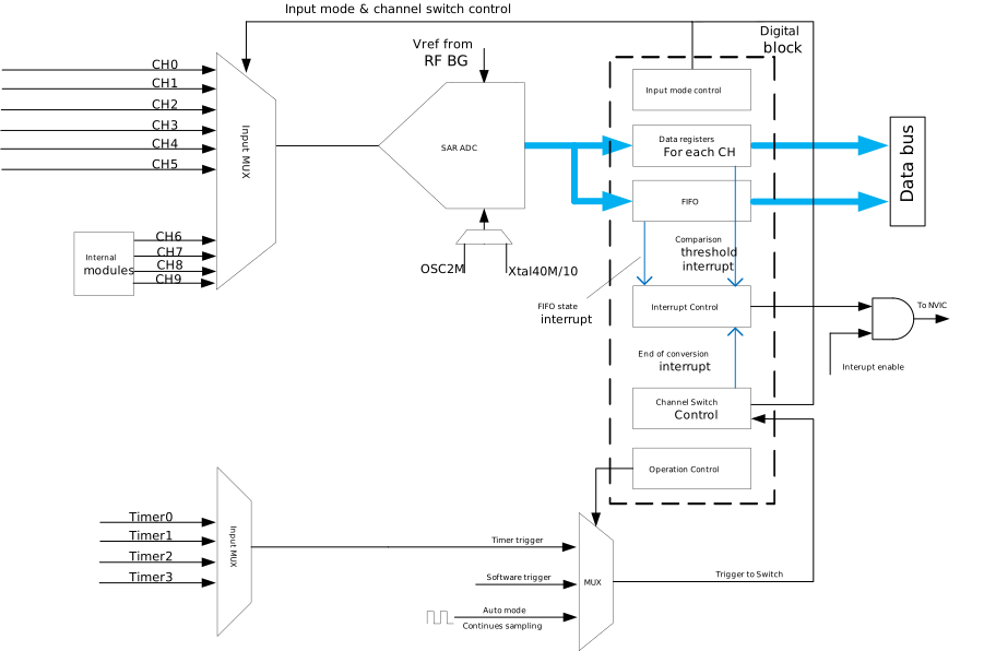
12 位 ADC 框图如下图所示。
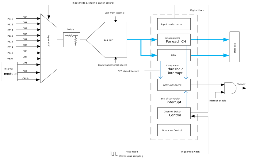
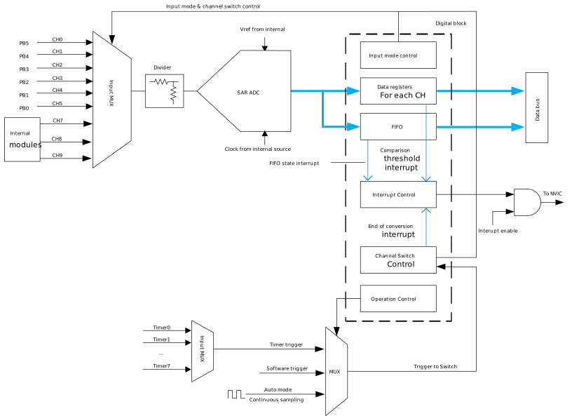
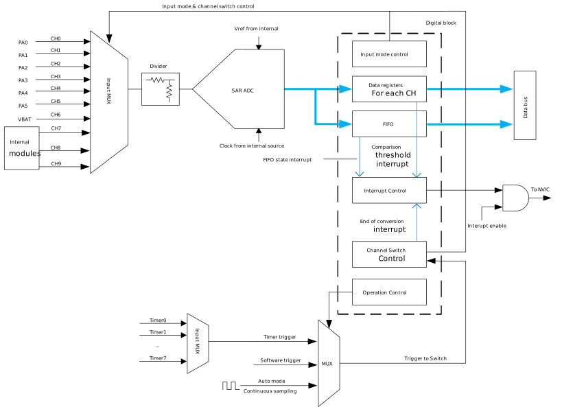
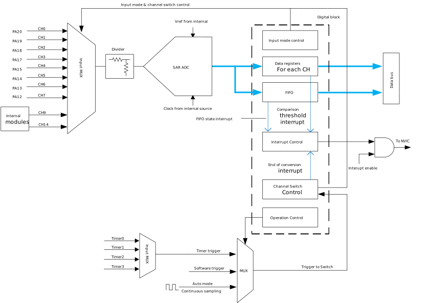
功能描述
通道切换列表
ADC 支持软件通过通道切换列表来配置完整的转换序列。软件可通过 REG_ADC_CHSW_LIST_0 和 REG_ADC_CHSW_LIST_1 两个寄存器指定待转换的目标通道编号,并通过配置寄存器 REG_ADC_CONF[7:4] 中的列表长度字段来设置序列中的通道总数。
例如,假设 REG_ADC_CHSW_LIST_0 与 REG_ADC_CHSW_LIST_1 的配置值如下表所示:
寄存器 |
[3:0] |
[7:4] |
[11:8] |
[15:12] |
[19:16] |
[23:20] |
[27:24] |
[31:28] |
|---|---|---|---|---|---|---|---|---|
REG_ADC_CHSW_LIST_0 |
0 |
1 |
2 |
3 |
4 |
5 |
9 |
0 |
REG_ADC_CHSW_LIST_1 |
1 |
9 |
5 |
4 |
3 |
2 |
1 |
0 |
若 REG_ADC_CONF[7:4] 设为 9,则 ADC 仅转换列表中的前 10 个(即 REG_ADC_CONF[7:4] + 1)通道。在自动模式下,ADC 将按顺序从列表中的首个通道依次转换至最后一个指定通道。当完成转换的通道数达到 REG_ADC_CONF[7:4] 设定的值后,ADC 将回到首个通道并重新开始下一轮转换序列(如下图所示)。
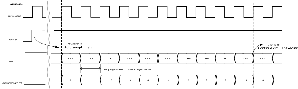
自动模式波形
REG_ADC_LAST_CH[3:0] 字段用于指示最近一次完成转换的通道,便于追踪转换序列的当前进度。此外,REG_ADC_BUSY_STS[0] 位用于指示 ADC 的忙碌状态;当 ADC 正在执行通道转换时,该位保持为 1。
工作模式
Ameba 仅支持一种工作模式:自动模式。
自动模式
在自动模式下,配置自动通道切换寄存器(REG_ADC_AUTO_CSW_CTRL[0])后,ADC 无需任何外部触发源即可连续执行转换。该模式会持续运行,直至自动通道切换寄存器被清除(REG_ADC_AUTO_CSW_CTRL[0])或自动通道切换功能被禁用(REG_ADC_CONF[3:1])。
自动模式下,ADC 由硬件自动完成采样,无需内核或其他模块介入。该模式适用于内核资源有限且需要实时检测的应用场景。自动模式的波形请参考 自动模式波形。
ADC 将按顺序扫描列表中的通道。相邻通道采样之间无时间间隔,扫描速度完全取决于 ADC 的采样率。在采样周期结束时,ADC 会立即将数据输出至寄存器和 FIFO,因此无需设置通道切换时间和建立时间。
当 REG_ADC_AUTO_CSW_CTRL[0] 置位时,采样数据会被连续填充到寄存器和 FIFO。若未被及时读取,数据将会丢失,且溢出的数据不会被继续写入 FIFO。对于需要间歇性从 FIFO 获取数据的场景,建议在读取前先清空 FIFO。
此外,有一种情况需特别注意:若 ADC 采样的信号源内阻较大,输入信号将极易受到干扰。
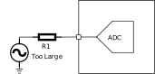
解决方案如下:
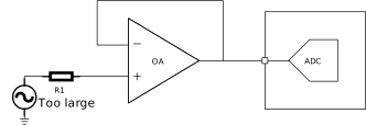
降低阻抗
如下图所示,可通过运算放大器(OA)提供极低的输出阻抗。
在通道列表中插入接地隔离通道
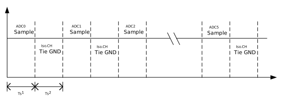
如下图所示,利用 GND 通道(内部 GND 通道或接地的外部通道),将 ADC 的通道列表配置为:CH0, CH_GND, CH1, CH_GND, CH2 ... CH5, CH_GND。此举可有效避免通道间的串扰,由此产生的通道间延迟取决于 ADC 的采样率及通道列表的配置。
Ameba 支持三种不同的工作模式:自动模式、定时器触发模式和软件触发模式。
尽管系统提供了多种模式以满足不同的应用需求,但同一时刻仅能激活一种工作模式。所有模式均基于通道切换列表来执行转换。这三种工作模式的主要区别在于驱动 ADC 模块执行转换的触发源不同。
自动模式
在自动模式下,配置自动通道切换寄存器(REG_ADC_AUTO_CSW_CTRL[0])后,ADC 无需任何外部触发源即可连续执行转换。该模式会持续运行,直至自动通道切换寄存器被清除(REG_ADC_AUTO_CSW_CTRL[0])或自动通道切换功能被禁用(REG_ADC_CONF[3:1])。
自动模式下,ADC 由硬件自动完成采样,无需内核或其他模块介入。该模式适用于内核资源有限且需要实时检测的应用场景。自动模式的波形请参考 自动模式波形。
ADC 将按顺序扫描列表中的通道。相邻通道采样之间无时间间隔,扫描速度完全取决于 ADC 的采样率。在采样周期结束时,ADC 会立即将数据输出至寄存器和 FIFO,因此无需设置通道切换时间和建立时间。
当 REG_ADC_AUTO_CSW_CTRL[0] 置位时,采样数据会被连续填充到寄存器和 FIFO。若未被及时读取,数据将会丢失,且溢出的数据不会被继续写入 FIFO。对于需要间歇性从 FIFO 获取数据的场景,建议在读取前先清空 FIFO。
此外,有一种情况需特别注意:若 ADC 采样的信号源内阻较大,输入信号将极易受到干扰。
解决方案如下:
降低阻抗
如下图所示,可通过运算放大器(OA)提供极低的输出阻抗。
在通道列表中插入接地隔离通道
如下图所示,利用 GND 通道(内部 GND 通道或接地的外部通道),将 ADC 的通道列表配置为:CH0, CH_GND, CH1, CH_GND, CH2 ... CH5, CH_GND。此举可有效避免通道间的串扰,由此产生的通道间延迟取决于 ADC 的采样率及通道列表的配置。
定时器触发模式
在定时器触发模式下,ADC 可结合定时器模块进行转换。软件通过设置定时器触发控制寄存器来启用定时器模块,并配置合适的定时器周期。此后,ADC 将根据系统设计,在每次定时器事件发生时执行转换。
与自动模式类似,定时器触发模式也可独立运行而无需软件干预,从而节省内核资源。此外,ADC 可以在两次定时器触发事件之间自动进入掉电(Power-down)模式,大幅降低 ADC 本身的功耗。定时器触发模式的波形请参考下图。
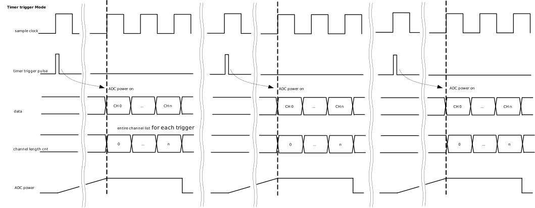
每次触发后,ADC 将上电并对通道列表中的通道执行采样转换,立即将转换结果存储至寄存器和 FIFO 中,随后 ADC 掉电。直到下一个触发信号到达,ADC 才会重新上电并执行采样转换。
因此,相邻两次触发之间的间隔时间受限于 ADC 的上电时间,建议该间隔不小于 1ms。若在 ADC 上电未完全时进行采样,可能会导致数据错误。上电完成后,ADC 会立即开始采样,采样周期由采样率决定。
与自动模式类似,在采样周期结束时,ADC 会立即将数据输出至寄存器和 FIFO。
备注
当前芯片最多支持 8 个定时器源(定时器 0~7)。
每次触发事件发生时,ADC 仅对通道列表中的一个通道进行采样。
软件触发模式
软件触发模式与定时器触发模式类似,主要区别在于触发源不同。在常规应用中,通常由软件来控制 ADC 的转换时序。每次置位软件触发寄存器(REG_ADC_SW_TRIG[0])时,ADC 模块会对列表中的通道执行采样转换。软件在读取转换数据寄存器(REG_ADC_DATA_GLOBAL)之前,需先检查就绪/忙碌状态寄存器(REG_ADC_BUSY_STS[0])。
相较于定时器触发模式,此模式更加灵活。软件可根据实际运行情况手动触发 ADC 采样,触发时间不固定。软件触发模式的波形请参考下图。
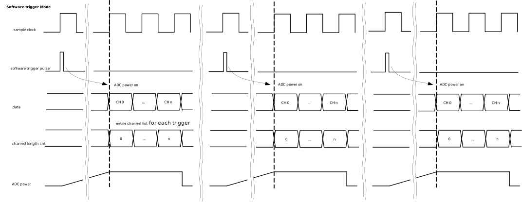
与定时器触发模式类似,在两次触发间隔期间,ADC 将进入睡眠状态,再次触发前需要重新上电。因此,触发间隔不宜过短,建议不小于 1ms。
备注
每次触发事件发生时,ADC 仅对通道列表中的一个通道进行采样。
总结
下表列出了不同工作模式的差异与应用场景。
工作模式 |
配置 |
区别 |
应用 |
|---|---|---|---|
自动模式 |
REG_ADC_CONF[3:1] = 1 |
|
适用于需实时检测且对功耗要求不高的场景。 |
定时器触发模式 |
REG_ADC_CONF[3:1] = 2 |
|
适用于需周期性检测且追求低功耗的场景。 |
软件触发模式 |
REG_ADC_CONF[3:1] = 0 REG_ADC_SW_TRIG[0] = 1 |
依赖软件触发但灵活性更高 |
适用于需根据当前环境灵活触发 ADC 采样的场景。 |
Ameba 支持三种不同的工作模式:自动模式、定时器触发模式和软件触发模式。
尽管系统提供了多种模式以满足不同的应用需求,但同一时刻仅能激活一种工作模式。所有模式均基于通道切换列表来执行转换。这三种工作模式的主要区别在于驱动 ADC 模块执行转换的触发源不同。
自动模式
在自动模式下,配置自动通道切换寄存器(REG_ADC_AUTO_CSW_CTRL[0])后,ADC 无需任何外部触发源即可连续执行转换。该模式会持续运行,直至自动通道切换寄存器被清除(REG_ADC_AUTO_CSW_CTRL[0])或自动通道切换功能被禁用(REG_ADC_CONF[3:1])。
自动模式下,ADC 由硬件自动完成采样,无需内核或其他模块介入。该模式适用于内核资源有限且需要实时检测的应用场景。自动模式的波形请参考 自动模式波形。
ADC 将按顺序扫描列表中的通道。相邻通道采样之间无时间间隔,扫描速度完全取决于 ADC 的采样率。在采样周期结束时,ADC 会立即将数据输出至寄存器和 FIFO,因此无需设置通道切换时间和建立时间。
当 REG_ADC_AUTO_CSW_CTRL[0] 置位时,采样数据会被连续填充到寄存器和 FIFO。若未被及时读取,数据将会丢失,且溢出的数据不会被继续写入 FIFO。对于需要间歇性从 FIFO 获取数据的场景,建议在读取前先清空 FIFO。
此外,有一种情况需特别注意:若 ADC 采样的信号源内阻较大,输入信号将极易受到干扰。
解决方案如下:
降低阻抗
如下图所示,可通过运算放大器(OA)提供极低的输出阻抗。
在通道列表中插入接地隔离通道
如下图所示,利用 GND 通道(内部 GND 通道或接地的外部通道),将 ADC 的通道列表配置为:CH0, CH_GND, CH1, CH_GND, CH2 ... CH5, CH_GND。此举可有效避免通道间的串扰,由此产生的通道间延迟取决于 ADC 的采样率及通道列表的配置。
定时器触发模式
在定时器触发模式下,ADC 可结合定时器模块进行转换。软件通过设置定时器触发控制寄存器来启用定时器模块,并配置合适的定时器周期。此后,ADC 将根据系统设计,在每次定时器事件发生时执行转换。
与自动模式类似,定时器触发模式也可独立运行而无需软件干预,从而节省内核资源。此外,ADC 可以在两次定时器触发事件之间自动进入掉电(Power-down)模式,大幅降低 ADC 本身的功耗。定时器触发模式的波形请参考下图。
每次触发后,ADC 将上电并对通道列表中的通道执行采样转换,立即将转换结果存储至寄存器和 FIFO 中,随后 ADC 掉电。直到下一个触发信号到达,ADC 才会重新上电并执行采样转换。
因此,相邻两次触发之间的间隔时间受限于 ADC 的上电时间,建议该间隔不小于 1ms。若在 ADC 上电未完全时进行采样,可能会导致数据错误。上电完成后,ADC 会立即开始采样,采样周期由采样率决定。
与自动模式类似,在采样周期结束时,ADC 会立即将数据输出至寄存器和 FIFO。
备注
当前芯片最多支持 8 个定时器源(定时器 0~7)。
每次触发事件发生时,ADC 仅对通道列表中的一个通道进行采样。
软件触发模式
软件触发模式与定时器触发模式类似,主要区别在于触发源不同。在常规应用中,通常由软件来控制 ADC 的转换时序。每次置位软件触发寄存器(REG_ADC_SW_TRIG[0])时,ADC 模块会对列表中的通道执行采样转换。软件在读取转换数据寄存器(REG_ADC_DATA_GLOBAL)之前,需先检查就绪/忙碌状态寄存器(REG_ADC_BUSY_STS[0])。
相较于定时器触发模式,此模式更加灵活。软件可根据实际运行情况手动触发 ADC 采样,触发时间不固定。软件触发模式的波形请参考下图。
与定时器触发模式类似,在两次触发间隔期间,ADC 将进入睡眠状态,再次触发前需要重新上电。因此,触发间隔不宜过短,建议不小于 1ms。
备注
每次触发事件发生时,ADC 仅对通道列表中的一个通道进行采样。
总结
下表列出了不同工作模式的差异与应用场景。
工作模式 |
配置 |
区别 |
应用 |
|---|---|---|---|
自动模式 |
REG_ADC_CONF[3:1] = 1 |
|
适用于需实时检测且对功耗要求不高的场景。 |
定时器触发模式 |
REG_ADC_CONF[3:1] = 2 |
|
适用于需周期性检测且追求低功耗的场景。 |
软件触发模式 |
REG_ADC_CONF[3:1] = 0 REG_ADC_SW_TRIG[0] = 1 |
依赖软件触发但灵活性更高 |
适用于需根据当前环境灵活触发 ADC 采样的场景。 |
Ameba 支持三种不同的工作模式:自动模式、定时器触发模式和软件触发模式。
尽管系统提供了多种模式以满足不同的应用需求,但同一时刻仅能激活一种工作模式。所有模式均基于通道切换列表来执行转换。这三种工作模式的主要区别在于驱动 ADC 模块执行转换的触发源不同。
自动模式
在自动模式下,配置自动通道切换寄存器(REG_ADC_AUTO_CSW_CTRL[0])后,ADC 无需任何外部触发源即可连续执行转换。该模式会持续运行,直至自动通道切换寄存器被清除(REG_ADC_AUTO_CSW_CTRL[0])或自动通道切换功能被禁用(REG_ADC_CONF[3:1])。
自动模式下,ADC 由硬件自动完成采样,无需内核或其他模块介入。该模式适用于内核资源有限且需要实时检测的应用场景。自动模式的波形请参考 自动模式波形。
ADC 将按顺序扫描列表中的通道。相邻通道采样之间无时间间隔,扫描速度完全取决于 ADC 的采样率。在采样周期结束时,ADC 会立即将数据输出至寄存器和 FIFO,因此无需设置通道切换时间和建立时间。
当 REG_ADC_AUTO_CSW_CTRL[0] 置位时,采样数据会被连续填充到寄存器和 FIFO。若未被及时读取,数据将会丢失,且溢出的数据不会被继续写入 FIFO。对于需要间歇性从 FIFO 获取数据的场景,建议在读取前先清空 FIFO。
此外,有一种情况需特别注意:若 ADC 采样的信号源内阻较大,输入信号将极易受到干扰。
解决方案如下:
降低阻抗
如下图所示,可通过运算放大器(OA)提供极低的输出阻抗。
在通道列表中插入接地隔离通道
如下图所示,利用 GND 通道(内部 GND 通道或接地的外部通道),将 ADC 的通道列表配置为:CH0, CH_GND, CH1, CH_GND, CH2 ... CH5, CH_GND。此举可有效避免通道间的串扰,由此产生的通道间延迟取决于 ADC 的采样率及通道列表的配置。
定时器触发模式
在定时器触发模式下,ADC 可结合定时器模块进行转换。软件通过设置定时器触发控制寄存器来启用定时器模块,并配置合适的定时器周期。此后,ADC 将根据系统设计,在每次定时器事件发生时执行转换。
与自动模式类似,定时器触发模式也可独立运行而无需软件干预,从而节省内核资源。此外,ADC 可以在两次定时器触发事件之间自动进入掉电(Power-down)模式,大幅降低 ADC 本身的功耗。定时器触发模式的波形请参考下图。
每次触发后,ADC 将上电并对通道列表中的通道执行采样转换,立即将转换结果存储至寄存器和 FIFO 中,随后 ADC 掉电。直到下一个触发信号到达,ADC 才会重新上电并执行采样转换。
因此,相邻两次触发之间的间隔时间受限于 ADC 的上电时间,建议该间隔不小于 1ms。若在 ADC 上电未完全时进行采样,可能会导致数据错误。上电完成后,ADC 会立即开始采样,采样周期由采样率决定。
与自动模式类似,在采样周期结束时,ADC 会立即将数据输出至寄存器和 FIFO。
备注
当前芯片最多支持 8 个定时器源(定时器 0~7)。
每次触发事件发生时,ADC 仅对通道列表中的一个通道进行采样。
软件触发模式
软件触发模式与定时器触发模式类似,主要区别在于触发源不同。在常规应用中,通常由软件来控制 ADC 的转换时序。每次置位软件触发寄存器(REG_ADC_SW_TRIG[0])时,ADC 模块会对列表中的通道执行采样转换。软件在读取转换数据寄存器(REG_ADC_DATA_GLOBAL)之前,需先检查就绪/忙碌状态寄存器(REG_ADC_BUSY_STS[0])。
相较于定时器触发模式,此模式更加灵活。软件可根据实际运行情况手动触发 ADC 采样,触发时间不固定。软件触发模式的波形请参考下图。
与定时器触发模式类似,在两次触发间隔期间,ADC 将进入睡眠状态,再次触发前需要重新上电。因此,触发间隔不宜过短,建议不小于 1ms。
备注
每次触发事件发生时,ADC 仅对通道列表中的一个通道进行采样。
总结
下表列出了不同工作模式的差异与应用场景。
工作模式 |
配置 |
区别 |
应用 |
|---|---|---|---|
自动模式 |
REG_ADC_CONF[3:1] = 1 |
|
适用于需实时检测且对功耗要求不高的场景。 |
定时器触发模式 |
REG_ADC_CONF[3:1] = 2 |
|
适用于需周期性检测且追求低功耗的场景。 |
软件触发模式 |
REG_ADC_CONF[3:1] = 0 REG_ADC_SW_TRIG[0] = 1 |
依赖软件触发但灵活性更高 |
适用于需根据当前环境灵活触发 ADC 采样的场景。 |
Ameba 支持三种不同的工作模式:自动模式、定时器触发模式和软件触发模式。
尽管系统提供了多种模式以满足不同的应用需求,但同一时刻仅能激活一种工作模式。所有模式均基于通道切换列表来执行转换。这三种工作模式的主要区别在于驱动 ADC 模块执行转换的触发源不同。
自动模式
在自动模式下,配置自动通道切换寄存器(REG_ADC_AUTO_CSW_CTRL[0])后,ADC 无需任何外部触发源即可连续执行转换。该模式会持续运行,直至自动通道切换寄存器被清除(REG_ADC_AUTO_CSW_CTRL[0])或自动通道切换功能被禁用(REG_ADC_CONF[3:1])。
自动模式下,ADC 由硬件自动完成采样,无需内核或其他模块介入。该模式适用于内核资源有限且需要实时检测的应用场景。自动模式的波形请参考 自动模式波形。
ADC 将按顺序扫描列表中的通道。相邻通道采样之间无时间间隔,扫描速度完全取决于 ADC 的采样率。在采样周期结束时,ADC 会立即将数据输出至寄存器和 FIFO,因此无需设置通道切换时间和建立时间。
当 REG_ADC_AUTO_CSW_CTRL[0] 置位时,采样数据会被连续填充到寄存器和 FIFO。若未被及时读取,数据将会丢失,且溢出的数据不会被继续写入 FIFO。对于需要间歇性从 FIFO 获取数据的场景,建议在读取前先清空 FIFO。
此外,有一种情况需特别注意:若 ADC 采样的信号源内阻较大,输入信号将极易受到干扰。
解决方案如下:
降低阻抗
如下图所示,可通过运算放大器(OA)提供极低的输出阻抗。
在通道列表中插入接地隔离通道
如下图所示,利用 GND 通道(内部 GND 通道或接地的外部通道),将 ADC 的通道列表配置为:CH0, CH_GND, CH1, CH_GND, CH2 ... CH5, CH_GND。此举可有效避免通道间的串扰,由此产生的通道间延迟取决于 ADC 的采样率及通道列表的配置。
定时器触发模式
在定时器触发模式下,ADC 可结合定时器模块进行转换。软件通过设置定时器触发控制寄存器来启用定时器模块,并配置合适的定时器周期。此后,ADC 将根据系统设计,在每次定时器事件发生时执行转换。
与自动模式类似,定时器触发模式也可独立运行而无需软件干预,从而节省内核资源。此外,ADC 可以在两次定时器触发事件之间自动进入掉电(Power-down)模式,大幅降低 ADC 本身的功耗。定时器触发模式的波形请参考下图。
每次触发后,ADC 将上电并对通道列表中的通道执行采样转换,立即将转换结果存储至寄存器和 FIFO 中,随后 ADC 掉电。直到下一个触发信号到达,ADC 才会重新上电并执行采样转换。
因此,相邻两次触发之间的间隔时间受限于 ADC 的上电时间,建议该间隔不小于 1ms。若在 ADC 上电未完全时进行采样,可能会导致数据错误。上电完成后,ADC 会立即开始采样,采样周期由采样率决定。
与自动模式类似,在采样周期结束时,ADC 会立即将数据输出至寄存器和 FIFO。
备注
当前芯片最多支持 8 个定时器源(定时器 0~7)。
每次触发事件发生时,ADC 仅对通道列表中的一个通道进行采样。
软件触发模式
软件触发模式与定时器触发模式类似,主要区别在于触发源不同。在常规应用中,通常由软件来控制 ADC 的转换时序。每次置位软件触发寄存器(REG_ADC_SW_TRIG[0])时,ADC 模块会对列表中的通道执行采样转换。软件在读取转换数据寄存器(REG_ADC_DATA_GLOBAL)之前,需先检查就绪/忙碌状态寄存器(REG_ADC_BUSY_STS[0])。
相较于定时器触发模式,此模式更加灵活。软件可根据实际运行情况手动触发 ADC 采样,触发时间不固定。软件触发模式的波形请参考下图。
与定时器触发模式类似,在两次触发间隔期间,ADC 将进入睡眠状态,再次触发前需要重新上电。因此,触发间隔不宜过短,建议不小于 1ms。
备注
每次触发事件发生时,ADC 仅对通道列表中的一个通道进行采样。
总结
下表列出了不同工作模式的差异与应用场景。
工作模式 |
配置 |
区别 |
应用 |
|---|---|---|---|
自动模式 |
REG_ADC_CONF[3:1] = 1 |
|
适用于需实时检测且对功耗要求不高的场景。 |
定时器触发模式 |
REG_ADC_CONF[3:1] = 2 |
|
适用于需周期性检测且追求低功耗的场景。 |
软件触发模式 |
REG_ADC_CONF[3:1] = 0 REG_ADC_SW_TRIG[0] = 1 |
依赖软件触发但灵活性更高 |
适用于需根据当前环境灵活触发 ADC 采样的场景。 |
Ameba 支持三种不同的工作模式:自动模式、定时器触发模式和软件触发模式。
尽管系统提供了多种模式以满足不同的应用需求,但同一时刻仅能激活一种工作模式。所有模式均基于通道切换列表来执行转换。这三种工作模式的主要区别在于驱动 ADC 模块执行转换的触发源不同。
自动模式
在自动模式下,配置自动通道切换寄存器(REG_ADC_AUTO_CSW_CTRL[0])后,ADC 无需任何外部触发源即可连续执行转换。该模式会持续运行,直至自动通道切换寄存器被清除(REG_ADC_AUTO_CSW_CTRL[0])或自动通道切换功能被禁用(REG_ADC_CONF[3:1])。
自动模式下,ADC 由硬件自动完成采样,无需内核或其他模块介入。该模式适用于内核资源有限且需要实时检测的应用场景。自动模式的波形请参考 自动模式波形。
ADC 将按顺序扫描列表中的通道。相邻通道采样之间无时间间隔,扫描速度完全取决于 ADC 的采样率。在采样周期结束时,ADC 会立即将数据输出至寄存器和 FIFO,因此无需设置通道切换时间和建立时间。
当 REG_ADC_AUTO_CSW_CTRL[0] 置位时,采样数据会被连续填充到寄存器和 FIFO。若未被及时读取,数据将会丢失,且溢出的数据不会被继续写入 FIFO。对于需要间歇性从 FIFO 获取数据的场景,建议在读取前先清空 FIFO。
此外,有一种情况需特别注意:若 ADC 采样的信号源内阻较大,输入信号将极易受到干扰。
解决方案如下:
降低阻抗
如下图所示,可通过运算放大器(OA)提供极低的输出阻抗。
在通道列表中插入接地隔离通道
如下图所示,利用 GND 通道(内部 GND 通道或接地的外部通道),将 ADC 的通道列表配置为:CH0, CH_GND, CH1, CH_GND, CH2 ... CH5, CH_GND。此举可有效避免通道间的串扰,由此产生的通道间延迟取决于 ADC 的采样率及通道列表的配置。
定时器触发模式
在定时器触发模式下,ADC 可结合定时器模块进行转换。软件通过设置定时器触发控制寄存器来启用定时器模块,并配置合适的定时器周期。此后,ADC 将根据系统设计,在每次定时器事件发生时执行转换。
与自动模式类似,定时器触发模式也可独立运行而无需软件干预,从而节省内核资源。此外,ADC 可以在两次定时器触发事件之间自动进入掉电(Power-down)模式,大幅降低 ADC 本身的功耗。定时器触发模式的波形请参考下图。
每次触发后,ADC 将上电并对通道列表中的通道执行采样转换,立即将转换结果存储至寄存器和 FIFO 中,随后 ADC 掉电。直到下一个触发信号到达,ADC 才会重新上电并执行采样转换。
因此,相邻两次触发之间的间隔时间受限于 ADC 的上电时间,建议该间隔不小于 1ms。若在 ADC 上电未完全时进行采样,可能会导致数据错误。上电完成后,ADC 会立即开始采样,采样周期由采样率决定。
与自动模式类似,在采样周期结束时,ADC 会立即将数据输出至寄存器和 FIFO。
备注
当前芯片最多支持 8 个定时器源(定时器 0~7)。
每次触发事件发生时,ADC 仅对通道列表中的一个通道进行采样。
软件触发模式
软件触发模式与定时器触发模式类似,主要区别在于触发源不同。在常规应用中,通常由软件来控制 ADC 的转换时序。每次置位软件触发寄存器(REG_ADC_SW_TRIG[0])时,ADC 模块会对列表中的通道执行采样转换。软件在读取转换数据寄存器(REG_ADC_DATA_GLOBAL)之前,需先检查就绪/忙碌状态寄存器(REG_ADC_BUSY_STS[0])。
相较于定时器触发模式,此模式更加灵活。软件可根据实际运行情况手动触发 ADC 采样,触发时间不固定。软件触发模式的波形请参考下图。
与定时器触发模式类似,在两次触发间隔期间,ADC 将进入睡眠状态,再次触发前需要重新上电。因此,触发间隔不宜过短,建议不小于 1ms。
备注
每次触发事件发生时,ADC 仅对通道列表中的一个通道进行采样。
总结
下表列出了不同工作模式的差异与应用场景。
工作模式 |
配置 |
区别 |
应用 |
|---|---|---|---|
自动模式 |
REG_ADC_CONF[3:1] = 1 |
|
适用于需实时检测且对功耗要求不高的场景。 |
定时器触发模式 |
REG_ADC_CONF[3:1] = 2 |
|
适用于需周期性检测且追求低功耗的场景。 |
软件触发模式 |
REG_ADC_CONF[3:1] = 0 REG_ADC_SW_TRIG[0] = 1 |
依赖软件触发但灵活性更高 |
适用于需根据当前环境灵活触发 ADC 采样的场景。 |
Ameba 支持三种不同的工作模式:自动模式、定时器触发模式和软件触发模式。
尽管系统提供了多种模式以满足不同的应用需求,但同一时刻仅能激活一种工作模式。所有模式均基于通道切换列表来执行转换。这三种工作模式的主要区别在于驱动 ADC 模块执行转换的触发源不同。
自动模式
在自动模式下,配置自动通道切换寄存器(REG_ADC_AUTO_CSW_CTRL[0])后,ADC 无需任何外部触发源即可连续执行转换。该模式会持续运行,直至自动通道切换寄存器被清除(REG_ADC_AUTO_CSW_CTRL[0])或自动通道切换功能被禁用(REG_ADC_CONF[3:1])。
自动模式下,ADC 由硬件自动完成采样,无需内核或其他模块介入。该模式适用于内核资源有限且需要实时检测的应用场景。自动模式的波形请参考 自动模式波形。
ADC 将按顺序扫描列表中的通道。相邻通道采样之间无时间间隔,扫描速度完全取决于 ADC 的采样率。在采样周期结束时,ADC 会立即将数据输出至寄存器和 FIFO,因此无需设置通道切换时间和建立时间。
当 REG_ADC_AUTO_CSW_CTRL[0] 置位时,采样数据会被连续填充到寄存器和 FIFO。若未被及时读取,数据将会丢失,且溢出的数据不会被继续写入 FIFO。对于需要间歇性从 FIFO 获取数据的场景,建议在读取前先清空 FIFO。
此外,有一种情况需特别注意:若 ADC 采样的信号源内阻较大,输入信号将极易受到干扰。
解决方案如下:
降低阻抗
如下图所示,可通过运算放大器(OA)提供极低的输出阻抗。
在通道列表中插入接地隔离通道
如下图所示,利用 GND 通道(内部 GND 通道或接地的外部通道),将 ADC 的通道列表配置为:CH0, CH_GND, CH1, CH_GND, CH2 ... CH5, CH_GND。此举可有效避免通道间的串扰,由此产生的通道间延迟取决于 ADC 的采样率及通道列表的配置。
备注
尽管 CH14(内部接地通道)被添加至通道列表中,但 CH14 的输出结果(固定为 0)并不会被存入 FIFO 中。因此,用户可以便捷地从 FIFO 中获取其他有效通道的采样数据。
定时器触发模式
在定时器触发模式下,ADC 可结合定时器模块进行转换。软件通过设置定时器触发控制寄存器来启用定时器模块,并配置合适的定时器周期。此后,ADC 将根据系统设计,在每次定时器事件发生时执行转换。
与自动模式类似,定时器触发模式也可独立运行而无需软件干预,从而节省内核资源。此外,ADC 可以在两次定时器触发事件之间自动进入掉电(Power-down)模式,大幅降低 ADC 本身的功耗。定时器触发模式的波形请参考下图。
每次触发后,ADC 将上电并对通道列表中的通道执行采样转换,立即将转换结果存储至寄存器和 FIFO 中,随后 ADC 掉电。直到下一个触发信号到达,ADC 才会重新上电并执行采样转换。
因此,相邻两次触发之间的间隔时间受限于 ADC 的上电时间,建议该间隔不小于 1ms。若在 ADC 上电未完全时进行采样,可能会导致数据错误。上电完成后,ADC 会立即开始采样,采样周期由采样率决定。
与自动模式类似,在采样周期结束时,ADC 会立即将数据输出至寄存器和 FIFO。
备注
当前芯片最多支持 4 个定时器源(定时器 0~3)。
每次触发事件发生时,ADC 对通道列表中的所有通道进行采样。
软件触发模式
软件触发模式与定时器触发模式类似,主要区别在于触发源不同。在常规应用中,通常由软件来控制 ADC 的转换时序。每次置位软件触发寄存器(REG_ADC_SW_TRIG[0])时,ADC 模块会对列表中的通道执行采样转换。软件在读取转换数据寄存器(REG_ADC_DATA_GLOBAL)之前,需先检查就绪/忙碌状态寄存器(REG_ADC_BUSY_STS[0])。
相较于定时器触发模式,此模式更加灵活。软件可根据实际运行情况手动触发 ADC 采样,触发时间不固定。软件触发模式的波形请参考下图。
与定时器触发模式类似,在两次触发间隔期间,ADC 将进入睡眠状态,再次触发前需要重新上电。因此,触发间隔不宜过短,建议不小于 1ms。
备注
每次生成触发源时,将对通道列表中的所有通道进行采样。
总结
下表列出了不同工作模式的差异与应用场景。
工作模式 |
配置 |
区别 |
应用 |
|---|---|---|---|
自动模式 |
REG_ADC_CONF[3:1] = 1 |
|
适用于需实时检测且对功耗要求不高的场景。 |
定时器触发模式 |
REG_ADC_CONF[3:1] = 2 |
|
适用于需周期性检测且追求低功耗的场景。 |
软件触发模式 |
REG_ADC_CONF[3:1] = 0 REG_ADC_SW_TRIG[0] = 1 |
依赖软件触发但灵活性更高 |
适用于需根据当前环境灵活触发 ADC 采样的场景。 |
Ameba 支持三种不同的工作模式:自动模式、定时器触发模式和软件触发模式。
尽管系统提供了多种模式以满足不同的应用需求,但同一时刻仅能激活一种工作模式。所有模式均基于通道切换列表来执行转换。这三种工作模式的主要区别在于驱动 ADC 模块执行转换的触发源不同。
自动模式
在自动模式下,配置自动通道切换寄存器(REG_ADC_AUTO_CSW_CTRL[0])后,ADC 无需任何外部触发源即可连续执行转换。该模式会持续运行,直至自动通道切换寄存器被清除(REG_ADC_AUTO_CSW_CTRL[0])或自动通道切换功能被禁用(REG_ADC_CONF[3:1])。
自动模式下,ADC 由硬件自动完成采样,无需内核或其他模块介入。该模式适用于内核资源有限且需要实时检测的应用场景。自动模式的波形请参考 自动模式波形。
ADC 将按顺序扫描列表中的通道。相邻通道采样之间无时间间隔,扫描速度完全取决于 ADC 的采样率。在采样周期结束时,ADC 会立即将数据输出至寄存器和 FIFO,因此无需设置通道切换时间和建立时间。
当 REG_ADC_AUTO_CSW_CTRL[0] 置位时,采样数据会被连续填充到寄存器和 FIFO。若未被及时读取,数据将会丢失,且溢出的数据不会被继续写入 FIFO。对于需要间歇性从 FIFO 获取数据的场景,建议在读取前先清空 FIFO。
此外,有一种情况需特别注意:若 ADC 采样的信号源内阻较大,输入信号将极易受到干扰。
解决方案如下:
降低阻抗
如下图所示,可通过运算放大器(OA)提供极低的输出阻抗。
在通道列表中插入接地隔离通道
如下图所示,利用 GND 通道(内部 GND 通道或接地的外部通道),将 ADC 的通道列表配置为:CH0, CH_GND, CH1, CH_GND, CH2 ... CH5, CH_GND。此举可有效避免通道间的串扰,由此产生的通道间延迟取决于 ADC 的采样率及通道列表的配置。
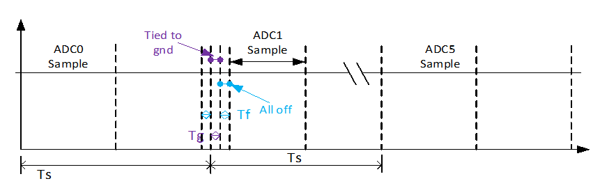
在前一个 ch 的转换时间插入接地隔离通道
如下图所示,每个通道都增加了一个比特位来控制是否选择 ISO 通道,并增加了一个相应的选择时间配置: 选择 ISO 通道 9,选择时间 Tg 可配置,与路径电容和电阻相关,默认值为 100ns,可调设置,全部关闭(未选择任何通道),选择时间 Tf 设置为 25ns
备注
尽管 CH9(内部接地通道)被添加至通道列表中,但 CH9 的输出结果(固定为 0)并不会被存入 FIFO 中。因此,用户可以便捷地从 FIFO 中获取其他有效通道的采样数据。
定时器触发模式
在定时器触发模式下,ADC 可结合定时器模块进行转换。软件通过设置定时器触发控制寄存器来启用定时器模块,并配置合适的定时器周期。此后,ADC 将根据系统设计,在每次定时器事件发生时执行转换。
与自动模式类似,定时器触发模式也可独立运行而无需软件干预,从而节省内核资源。此外,ADC 可以在两次定时器触发事件之间自动进入掉电(Power-down)模式,大幅降低 ADC 本身的功耗。定时器触发模式的波形请参考下图。
每次触发后,ADC 将上电并对通道列表中的通道执行采样转换,立即将转换结果存储至寄存器和 FIFO 中,随后 ADC 掉电。直到下一个触发信号到达,ADC 才会重新上电并执行采样转换。
因此,相邻两次触发之间的间隔时间受限于 ADC 的上电时间,建议该间隔不小于 1ms。若在 ADC 上电未完全时进行采样,可能会导致数据错误。上电完成后,ADC 会立即开始采样,采样周期由采样率决定。
与自动模式类似,在采样周期结束时,ADC 会立即将数据输出至寄存器和 FIFO。
备注
当前芯片最多支持 4 个定时器源(定时器 0~3)。
每次触发事件发生时,ADC 对通道列表中的所有通道进行采样。
软件触发模式
软件触发模式与定时器触发模式类似,主要区别在于触发源不同。在常规应用中,通常由软件来控制 ADC 的转换时序。每次置位软件触发寄存器(REG_ADC_SW_TRIG[0])时,ADC 模块会对列表中的通道执行采样转换。软件在读取转换数据寄存器(REG_ADC_DATA_GLOBAL)之前,需先检查就绪/忙碌状态寄存器(REG_ADC_BUSY_STS[0])。
相较于定时器触发模式,此模式更加灵活。软件可根据实际运行情况手动触发 ADC 采样,触发时间不固定。软件触发模式的波形请参考下图。
与定时器触发模式类似,在两次触发间隔期间,ADC 将进入睡眠状态,再次触发前需要重新上电。因此,触发间隔不宜过短,建议不小于 1ms。
备注
每次生成触发源时,将对通道列表中的所有通道进行采样。
总结
下表列出了不同工作模式的差异与应用场景。
工作模式 |
配置 |
区别 |
应用 |
|---|---|---|---|
自动模式 |
REG_ADC_CONF[3:1] = 1 |
|
适用于需实时检测且对功耗要求不高的场景。 |
定时器触发模式 |
REG_ADC_CONF[3:1] = 2 |
|
适用于需周期性检测且追求低功耗的场景。 |
软件触发模式 |
REG_ADC_CONF[3:1] = 0 REG_ADC_SW_TRIG[0] = 1 |
依赖软件触发但灵活性更高 |
适用于需根据当前环境灵活触发 ADC 采样的场景。 |
低功耗时钟源
下图展示了 ADC 的时钟结构。用户可通过配置寄存器 REG_ADC_CLK_DIV[2:0] 来设定 ADC 的采样频率。ADC 支持 OSC 和 XTAL 两种不同的时钟源,其中,XTAL 时钟的性能更好,而 OSC 时钟具有更低的功耗。
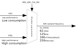
系统进入低功耗状态后,可以通过 ADC 自动模式完成采样,并利用 ADC 中断唤醒系统。
自动模式下,ADC 硬件自动连续对外部模拟电压进行采样。用户可以预设高/低阈值以及比较标准。整个过程 CPU 完全休眠,只有当采样电压符合预设的电压比较标准时,系统才会被唤醒。
低功耗状态下,仅支持 OSC 时钟作为 ADC 时钟源,此时系统可以被唤醒。
备注
RTL8721Dx 在低功耗状态下仅支持自动模式。
下图展示了 ADC 的时钟结构。用户可通过配置寄存器 REG_ADC_CLK_DIV[2:0] 来设定 ADC 的采样频率。ADC 支持 OSC 和 XTAL 两种不同的时钟源,其中,XTAL 时钟的性能更好,而 OSC 时钟具有更低的功耗。
系统进入低功耗状态后,可以通过 ADC 自动模式或者定时器触发模式完成采样,并利用 ADC 中断唤醒系统。
自动模式:ADC 硬件自动连续对外部模拟电压进行采样。用户可以预设高/低阈值以及比较标准。整个过程 CPU 完全休眠,只有当采样电压符合预设的电压比较标准时,系统才会被唤醒。
定时器触发模式:低功耗状态下,定时器每隔一段时间自动发送信号触发 ADC 进行一次采样,采样完成的同时可以唤醒系统。
低功耗状态下,仅支持 OSC 时钟作为 ADC 时钟源,此时系统可以被唤醒。
下图展示了 ADC 的时钟结构。用户可通过配置寄存器 REG_ADC_CLK_DIV[2:0] 来设定 ADC 的采样频率。ADC 支持 OSC 和 XTAL 两种不同的时钟源,其中,XTAL 时钟的性能更好,而 OSC 时钟具有更低的功耗。
系统进入低功耗状态后,可以通过 ADC 自动模式或者定时器触发模式完成采样,并利用 ADC 中断唤醒系统。
自动模式:ADC 硬件自动连续对外部模拟电压进行采样。用户可以预设高/低阈值以及比较标准。整个过程 CPU 完全休眠,只有当采样电压符合预设的电压比较标准时,系统才会被唤醒。
定时器触发模式:低功耗状态下,定时器每隔一段时间自动发送信号触发 ADC 进行一次采样,采样完成的同时可以唤醒系统。
低功耗状态下,仅支持 OSC 时钟作为 ADC 时钟源,此时系统可以被唤醒。
下图展示了 ADC 的时钟结构。用户可通过配置寄存器 REG_ADC_CLK_DIV[2:0] 来设定 ADC 的采样频率。ADC 支持 OSC 和 XTAL 两种不同的时钟源,其中,XTAL 时钟的性能更好,而 OSC 时钟具有更低的功耗。
系统进入低功耗状态后,可以通过 ADC 自动模式或者定时器触发模式完成采样,并利用 ADC 中断唤醒系统。
自动模式:ADC 硬件自动连续对外部模拟电压进行采样。用户可以预设高/低阈值以及比较标准。整个过程 CPU 完全休眠,只有当采样电压符合预设的电压比较标准时,系统才会被唤醒。
定时器触发模式:低功耗状态下,定时器每隔一段时间自动发送信号触发 ADC 进行一次采样,采样完成的同时可以唤醒系统。
低功耗状态下,仅支持 OSC 时钟作为 ADC 时钟源,此时系统可以被唤醒。
下图展示了 ADC 的时钟结构。用户可通过配置寄存器 REG_ADC_CLK_DIV[2:0] 来设定 ADC 的采样频率。ADC 支持 OSC 和 XTAL 两种不同的时钟源,其中,XTAL 时钟的性能更好,而 OSC 时钟具有更低的功耗。
系统进入低功耗状态后,可以通过 ADC 自动模式或者定时器触发模式完成采样,并利用 ADC 中断唤醒系统。
自动模式:ADC 硬件自动连续对外部模拟电压进行采样。用户可以预设高/低阈值以及比较标准。整个过程 CPU 完全休眠,只有当采样电压符合预设的电压比较标准时,系统才会被唤醒。
定时器触发模式:低功耗状态下,定时器每隔一段时间自动发送信号触发 ADC 进行一次采样,采样完成的同时可以唤醒系统。
低功耗状态下,仅支持 OSC 时钟作为 ADC 时钟源,此时系统可以被唤醒。
下图展示了 ADC 的时钟结构。用户可通过配置寄存器 REG_ADC_CLK_DIV[2:0] 来设定 ADC 的采样频率。ADC 支持 OSC 和 XTAL 两种不同的时钟源,其中,XTAL 时钟的性能更好,而 OSC 时钟具有更低的功耗。
系统进入低功耗状态后,可以通过 ADC 自动模式或者定时器触发模式完成采样,并利用 ADC 中断唤醒系统。
自动模式:ADC 硬件自动连续对外部模拟电压进行采样。用户可以预设高/低阈值以及比较标准。整个过程 CPU 完全休眠,只有当采样电压符合预设的电压比较标准时,系统才会被唤醒。
定时器触发模式:低功耗状态下,定时器每隔一段时间自动发送信号触发 ADC 进行一次采样,采样完成的同时可以唤醒系统。
低功耗状态下,仅支持 OSC 时钟作为 ADC 时钟源,此时系统可以被唤醒。
备注
若选择 OSC 作为 ADC 时钟源,需在 ameba_sleepcfg.c 中将 ps_config 中的 keep_osc4m_on 设置为 TRUE。
下图展示了 ADC 的时钟结构。用户可通过配置 REG_ADC_CLK_HCNTx 和 REG_ADC_CLK_LCNT0_DIV 寄存器,来设定每个 ADC 通道的采样时长与转换时长。ADC 支持 OSC 和 XTAL 两种不同的时钟源,其中,XTAL 时钟的性能更好,而 OSC 时钟具有更低的功耗。
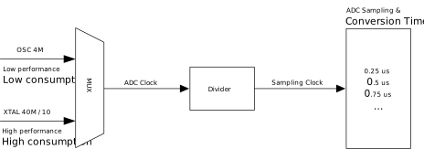
系统进入低功耗状态后,可以通过 ADC 自动模式或者定时器触发模式完成采样,并利用 ADC 中断唤醒系统。
自动模式:ADC 硬件自动连续对外部模拟电压进行采样。用户可以预设高/低阈值以及比较标准。整个过程 CPU 完全休眠,只有当采样电压符合预设的电压比较标准时,系统才会被唤醒。
定时器触发模式:低功耗状态下,定时器每隔一段时间自动发送信号触发 ADC 进行一次采样,采样完成的同时可以唤醒系统。
低功耗状态下,仅支持 OSC 时钟作为 ADC 时钟源,此时系统可以被唤醒。
下图展示了 ADC 的时钟结构。用户可通过配置 REG_ADC_CLK_HCNTx 和 REG_ADC_CLK_LCNT0_DIV 寄存器,来设定每个 ADC 通道的采样时长与转换时长。ADC 支持 OSC 和 XTAL 两种不同的时钟源,其中,XTAL 时钟的性能更好,而 OSC 时钟具有更低的功耗。
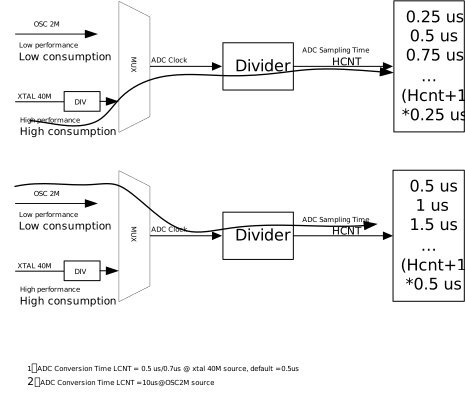
系统进入低功耗状态后,可以通过 ADC 自动模式或者定时器触发模式完成采样,并利用 ADC 中断唤醒系统。
自动模式:ADC 硬件自动连续对外部模拟电压进行采样。用户可以预设高/低阈值以及比较标准。整个过程 CPU 完全休眠,只有当采样电压符合预设的电压比较标准时,系统才会被唤醒。
定时器触发模式:低功耗状态下,定时器每隔一段时间自动发送信号触发 ADC 进行一次采样,采样完成的同时可以唤醒系统。
各通道的独立比较事件
ADC 可用于实现电压监测功能。ADC 的每个通道均可配置两个独立的比较阈值以及不同的比较标准。当 ADC 的采样值满足设定条件时,可通过 REG_ADC_INTR_STS 寄存器检测到相应中断。
各通道的阈值(包含高阈值与低阈值)可在 REG_ADC_COMP_TH_CHx 寄存器中进行配置。各通道的比较标准则在 REG_ADC_COMP_CTRL 寄存器中配置。ADC 比较功能支持以下四种不同的比较标准:
Vin < bit_adc_comp_th_l_chx
Vin > bit_adc_comp_th_h_chx
Vin >= bit_adc_comp_th_l_chx 且 Vin <= bit_adc_comp_th_h_chx
Vin < bit_adc_comp_th_l_chx 或 Vin > bit_adc_comp_th_h_chx
例如,当配置为 Vin < bit_adc_comp_th_l_chx 或 Vin > bit_adc_comp_th_h_chx 时,若 ADC 的转换数据低于低阈值或高于高阈值,系统将触发中断事件。
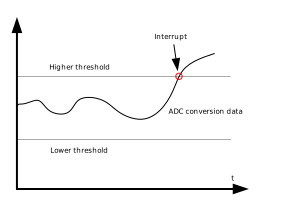
ADC 支持两种不同的中断触发模式(电平检测和边沿检测),以将比较匹配事件通知给 CPU。其中,电平检测会持续上报中断,边沿检测仅在中断发生时上报一次。
ADC 支持两种不同的中断触发模式(电平检测和边沿检测),以将比较匹配事件通知给 CPU。其中,电平检测会持续上报中断,边沿检测仅在中断发生时上报一次。
ADC 支持两种不同的中断触发模式(电平检测和边沿检测),以将比较匹配事件通知给 CPU。其中,电平检测会持续上报中断,边沿检测仅在中断发生时上报一次。
ADC 支持两种不同的中断触发模式(电平检测和边沿检测),以将比较匹配事件通知给 CPU。其中,电平检测会持续上报中断,边沿检测仅在中断发生时上报一次。
ADC 支持两种不同的中断触发模式(电平检测和边沿检测),以将比较匹配事件通知给 CPU。其中,电平检测会持续上报中断,边沿检测仅在中断发生时上报一次。
ADC 仅支持电平检测中断触发模式,以将比较匹配事件通知给 CPU, 电平检测会持续上报中断。
ADC 支持两种不同的中断触发模式(电平检测和边沿检测),以将比较匹配事件通知给 CPU。其中,电平检测会持续上报中断,边沿检测仅在中断发生时上报一次。
ADC 支持两种不同的中断触发模式(电平检测和边沿检测),以将比较匹配事件通知给 CPU。其中,电平检测会持续上报中断,边沿检测仅在中断发生时上报一次。
采样结果的获取
FIFO
用户可通过读取 REG_ADC_DATA_GLOBAL 寄存器从 ADC FIFO 中获取采样结果。ADC 会将所有采样结果存储至 FIFO 中。ADC FIFO 共包含 64 个条目,每个 20 位的 FIFO 数据条目由 4 位通道号和 16 位转换数据组成,如下图所示。
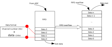
FIFO 充当了运行速率不同的数据采集系统与数据处理系统之间的缓冲区,因此,及时读取数据对于防止数据丢失至关重要。
在正常运行期间,ADC 会持续将数据写入 FIFO,同时软件从中读取数据。若软件读取数据的速度慢于 ADC 写入数据的速度,则会导致 FIFO 溢出。如上图所示,在发生溢出的情况下,任何新采样的数据均会被丢弃,而不会写入 FIFO。
用户可通过读取 REG_ADC_DATA_GLOBAL 寄存器从 ADC FIFO 中获取采样结果。ADC 会将所有采样结果存储至 FIFO 中。ADC FIFO 共包含 64 个条目,每个 16 位的 FIFO 数据条目由 4 位通道号和 12 位转换数据组成,如下图所示。
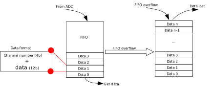
FIFO 充当了运行速率不同的数据采集系统与数据处理系统之间的缓冲区,因此,及时读取数据对于防止数据丢失至关重要。
在正常运行期间,ADC 会持续将数据写入 FIFO,同时软件从中读取数据。若软件读取数据的速度慢于 ADC 写入数据的速度,则会导致 FIFO 溢出。如上图所示,在发生溢出的情况下,任何新采样的数据均会被丢弃,而不会写入 FIFO。
用户可通过读取 REG_ADC_DATA_GLOBAL 寄存器从 ADC FIFO 中获取采样结果。ADC 会将所有采样结果存储至 FIFO 中。ADC FIFO 共包含 64 个条目,每个 16 位的 FIFO 数据条目由 4 位通道号和 12 位转换数据组成,如下图所示。
FIFO 充当了运行速率不同的数据采集系统与数据处理系统之间的缓冲区,因此,及时读取数据对于防止数据丢失至关重要。
在正常运行期间,ADC 会持续将数据写入 FIFO,同时软件从中读取数据。若软件读取数据的速度慢于 ADC 写入数据的速度,则会导致 FIFO 溢出。如上图所示,在发生溢出的情况下,任何新采样的数据均会被丢弃,而不会写入 FIFO。
用户可通过读取 REG_ADC_DATA_GLOBAL 寄存器从 ADC FIFO 中获取采样结果。ADC 会将所有采样结果存储至 FIFO 中。ADC FIFO 共包含 64 个条目,每个 16 位的 FIFO 数据条目由 4 位通道号和 12 位转换数据组成,如下图所示。
FIFO 充当了运行速率不同的数据采集系统与数据处理系统之间的缓冲区,因此,及时读取数据对于防止数据丢失至关重要。
在正常运行期间,ADC 会持续将数据写入 FIFO,同时软件从中读取数据。若软件读取数据的速度慢于 ADC 写入数据的速度,则会导致 FIFO 溢出。如上图所示,在发生溢出的情况下,任何新采样的数据均会被丢弃,而不会写入 FIFO。
用户可通过读取 REG_ADC_DATA_GLOBAL 寄存器从 ADC FIFO 中获取采样结果。ADC 会将所有采样结果存储至 FIFO 中。ADC FIFO 共包含 64 个条目,每个 16 位的 FIFO 数据条目由 4 位通道号和 12 位转换数据组成,如下图所示。
FIFO 充当了运行速率不同的数据采集系统与数据处理系统之间的缓冲区,因此,及时读取数据对于防止数据丢失至关重要。
在正常运行期间,ADC 会持续将数据写入 FIFO,同时软件从中读取数据。若软件读取数据的速度慢于 ADC 写入数据的速度,则会导致 FIFO 溢出。如上图所示,在发生溢出的情况下,任何新采样的数据均会被丢弃,而不会写入 FIFO。
用户可通过读取 REG_ADC_DATA_GLOBAL 寄存器从 ADC FIFO 中获取采样结果。ADC 会将所有采样结果存储至 FIFO 中。ADC FIFO 共包含 64 个条目,每个 16 位的 FIFO 数据条目由 4 位通道号和 12 位转换数据组成,如下图所示。
FIFO 充当了运行速率不同的数据采集系统与数据处理系统之间的缓冲区,因此,及时读取数据对于防止数据丢失至关重要。
在正常运行期间,ADC 会持续将数据写入 FIFO,同时软件从中读取数据。若软件读取数据的速度慢于 ADC 写入数据的速度,则会导致 FIFO 溢出。如上图所示,在发生溢出的情况下,任何新采样的数据均会被丢弃,而不会写入 FIFO。
用户可通过读取 REG_ADC_DATA_GLOBAL 寄存器从 ADC FIFO 中获取采样结果。ADC 会将所有采样结果存储至 FIFO 中。ADC FIFO 共包含 64 个条目,每个 20 位的 FIFO 数据条目由 4 位通道号和 16 位转换数据组成,如下图所示。
FIFO 充当了运行速率不同的数据采集系统与数据处理系统之间的缓冲区,因此,及时读取数据对于防止数据丢失至关重要。
在正常运行期间,ADC 会持续将数据写入 FIFO,同时软件从中读取数据。若软件读取数据的速度慢于 ADC 写入数据的速度,则会导致 FIFO 溢出。如上图所示,在发生溢出的情况下,任何新采样的数据均会被丢弃,而不会写入 FIFO。
用户可通过读取 REG_ADC_DATA_GLOBAL 寄存器从 ADC FIFO 中获取采样结果。ADC 会将所有采样结果存储至 FIFO 中。ADC FIFO 共包含 64 个条目,每个 20 位的 FIFO 数据条目由 4 位通道号和 16 位转换数据组成,如下图所示。
FIFO 充当了运行速率不同的数据采集系统与数据处理系统之间的缓冲区,因此,及时读取数据对于防止数据丢失至关重要。
在正常运行期间,ADC 会持续将数据写入 FIFO,同时软件从中读取数据。若软件读取数据的速度慢于 ADC 写入数据的速度,则会导致 FIFO 溢出。如上图所示,在发生溢出的情况下,任何新采样的数据均会被丢弃,而不会写入 FIFO。
除了及时获取数据以避免溢出外,强烈建议在启动任何新的数据采样流程之前,先通过置位 REG_ADC_CLR_FIFO[0] 来清空 ADC FIFO。
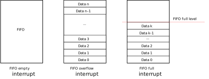
若启用了 FIFO 溢出中断(ADC_BIT_IT_FIFO_OVER_EN),当 FIFO 发生溢出时,系统将向 NVIC 发送中断信号。同理,若启用了 FIFO 空中断(ADC_BIT_IT_FIFO_EMPTY_EN),当 FIFO 为空时也会触发相应中断。
此外,用户可通过配置 REG_ADC_FULL_LVL[5:0] 来自定义 FIFO 满阈值。在启用 FIFO 满中断(ADC_BIT_IT_FIFO_FULL_EN)的情况下,一旦 FIFO 中的数据量达到此设定阈值,模块便会向 NVIC 发送中断信号,如下图所示。
REG_ADC_FLR[5:0] 用于指示当前 ADC FIFO 中的数据量。
独立通道寄存器
每个通道均配备独立的数据寄存器,用于存储其最新的转换结果。此类寄存器统一命名为 REG_ADC_DATA_CHx,其中 x 代表具体的通道编号(例如 CH0)。
REG_ADC_DATA_CHx[15:0] 包含 CHx 的最新转换数据。
REG_ADC_DATA_CHx[19:16] 指示与最新转换数据相关联的通道编号。
REG_ADC_DATA_CHx[20] 为指示数据覆盖事件的标志位。
REG_ADC_DATA_CHx[21] 为指示转换完成的标志位。
REG_ADC_DATA_CHx[11:0] 包含 CHx 的最新转换数据。
REG_ADC_DATA_CHx[15:12] 指示与最新转换数据相关联的通道编号。
REG_ADC_DATA_CHx[16] 为指示数据覆盖事件的标志位。
REG_ADC_DATA_CHx[17] 为指示转换完成的标志位。
REG_ADC_DATA_CHx[11:0] 包含 CHx 的最新转换数据。
REG_ADC_DATA_CHx[15:12] 指示与最新转换数据相关联的通道编号。
REG_ADC_DATA_CHx[16] 为指示数据覆盖事件的标志位。
REG_ADC_DATA_CHx[17] 为指示转换完成的标志位。
REG_ADC_DATA_CHx[11:0] 包含 CHx 的最新转换数据。
REG_ADC_DATA_CHx[15:12] 指示与最新转换数据相关联的通道编号。
REG_ADC_DATA_CHx[16] 为指示数据覆盖事件的标志位。
REG_ADC_DATA_CHx[17] 为指示转换完成的标志位。
REG_ADC_DATA_CHx[11:0] 包含 CHx 的最新转换数据。
REG_ADC_DATA_CHx[15:12] 指示与最新转换数据相关联的通道编号。
REG_ADC_DATA_CHx[16] 为指示数据覆盖事件的标志位。
REG_ADC_DATA_CHx[17] 为指示转换完成的标志位。
REG_ADC_DATA_CHx[11:0] 包含 CHx 的最新转换数据。
REG_ADC_DATA_CHx[15:12] 指示与最新转换数据相关联的通道编号。
REG_ADC_DATA_CHx[16] 为指示数据覆盖事件的标志位。
REG_ADC_DATA_CHx[17] 为指示转换完成的标志位。
REG_ADC_DATA_CHx[15:0] 包含 CHx 的最新转换数据。
REG_ADC_DATA_CHx[19:16] 指示与最新转换数据相关联的通道编号。
REG_ADC_DATA_CHx[20] 为指示数据覆盖事件的标志位。
REG_ADC_DATA_CHx[21] 为指示转换完成的标志位。
REG_ADC_DATA_CHx[15:0] 包含 CHx 的最新转换数据。
REG_ADC_DATA_CHx[19:16] 指示与最新转换数据相关联的通道编号。
REG_ADC_DATA_CHx[20] 为指示数据覆盖事件的标志位。
REG_ADC_DATA_CHx[21] 为指示转换完成的标志位。
PAD 配置
ADC 的模拟前端 (AFE) 属于模拟器件,模拟信号经由芯片引脚输入至芯片内部。因此,在此信号路径上应避免明显的数字信号干扰,且不应存在上拉或下拉电路。
若用户需将 GPIO 引脚复用为 ADC 输入引脚,除了将引脚功能配置为 ADC 外,还需禁用所选引脚的数字电路功能,并将其设置为无上拉/下拉状态(包括在睡眠模式下)。
校准
每颗芯片的 ADC 在出厂前均已完成校准。用户可通过调用 ADC_GetVoltage() 函数并将转换数据作为参数传入,直接获取经校准的精确电压转换结果。
寄存器
Base Address: 0x41011000
Name |
Address offset |
Access |
Description |
|---|---|---|---|
000h |
R/W |
The basic configuration of ADC includes enable and operation mode. |
|
004h |
R/W |
This register is used to configure analog ADC input type. |
|
008h |
R/W |
||
00Ch |
R/W |
||
010h |
R/W |
||
014h |
R/W |
||
018h |
R/W |
||
01Ch |
R/W |
||
020h |
R/W |
||
024h |
R/W |
||
028h |
R/W |
||
02Ch |
R/W |
||
030h |
R/W |
||
034h |
R/W |
This is channel comparison criterion control register, which can be used to control every channel's comparison criterion. There are 3 kinds of criterions. |
|
038h |
R |
This is the register about comparison status of every channel. |
|
03Ch |
R/W |
Software channel list 0, used to define the analog channels to own channel list. |
|
040h |
R/W |
Software channel list 1, refer to REG_ADC_CHSW_LIST_0. |
|
048h |
R/W |
This is the register about automatic switch channel function. |
|
04Ch |
R/W |
Software controls to trigger the channel switch. |
|
050h |
R |
This register records the last channel. |
|
054h |
R |
This register reflects the ADC FSM and FIFO status. |
|
058h |
R/W |
This register is used to enable or disable the different kinds of interrupts. |
|
05Ch |
R |
This register is used to record the different kinds of interrupt raw status (bypass the enable register's control). |
|
060h |
R/W |
This register is used to record the different kinds of interrupt status. |
|
064h |
R/W |
This register is about the specific channel to trigger interrupts. |
|
068h |
R/W |
||
06Ch |
R/W |
This register is used to select the specific external timer source. |
|
070h |
R |
This register is used to store the channel data, ready and overwritten information. |
|
074h |
R |
This register is used to store the channel data, ready and overwritten information. |
|
078h |
R |
This register is used to store the channel data, ready and overwritten information. |
|
07Ch |
R |
This register is used to store the channel data, ready and overwritten information. |
|
080h |
R |
This register is used to store the channel data, ready and overwritten information. |
|
084h |
R |
This register is used to store the channel data, ready and overwritten information. |
|
088h |
R |
This register is used to store the channel data, ready and overwritten information. |
|
08Ch |
R |
This register is used to store the channel data, ready and overwritten information. |
|
090h |
R |
This register is used to store the channel data, ready and overwritten information. |
|
094h |
R |
This register is used to store the channel data, ready and overwritten information. |
|
098h |
R |
This register is used to store the channel data, ready and overwritten information. |
|
09Ch |
R |
This register is used to store global data, ready, channel and overwritten information. |
|
0A0h |
R |
This register is used to store FIFO entry number. |
|
0A4h |
R/W |
This register is used to clear FIFO. |
|
0A8h |
R/W |
This register is used to control clock dividend and channel unmask. |
|
0ACh |
R/W |
This register is used to configure ADC over sample. |
|
0B0h |
R/W |
This register is used to control the ADC power and debug configuration. |
|
0B4h |
R/W |
This register is used to set the software test mode. |
|
0B8h |
R/W |
REG_ADC_CONF
Name: ADC Configuration Register
Size: 32
Address offset: 000h
Read/write access: R/W
The basic configuration of ADC includes enable and operation mode.
Bit |
Symbol |
Access |
INI |
Description |
|---|---|---|---|---|
31:10 |
RSVD |
R |
- |
Reserved |
9 |
BIT_ADC_ENABLE |
R/W |
0h |
This bit is for ADC enable control |
8 |
RSVD |
R |
- |
Reserved |
7:4 |
BIT_ADC_CVLIST_LEN |
R/W |
0h |
This field defines the number of items in the ADC conversion channel list. |
3:1 |
BIT_ADC_OP_MOD |
R/W |
0h |
These bits selects ADC operation mode.
|
0 |
RSVD |
R |
- |
Reserved |
REG_ADC_IN_TYPE
Name: ADC Input Type Register
Size: 32
Address offset: 004h
Read/write access: R/W
This register is used to configure analog ADC input type.
Bit |
Symbol |
Access |
INI |
Description |
|---|---|---|---|---|
31:11 |
RSVD |
R |
- |
Reserved |
10 |
BIT_ADC_IN_TYPE_CH10 |
R |
0 |
This bit reflects which kind of input type channel 10 is. Since channel 10 is a fixed internal channel. |
9 |
BIT_ADC_IN_TYPE_CH9 |
R |
0 |
This bit reflects which kind of input type channel 9 is. Since channel 9 is a fixed internal channel. |
8 |
BIT_ADC_IN_TYPE_CH8 |
R |
0 |
This bit reflects which kind of input type channel 8 is. Since channel 8 is a fixed internal channel. |
7 |
BIT_ADC_IN_TYPE_CH7 |
R |
0 |
This bit reflects which kind of input type channel 7 is. Since channel 7 is a fixed internal channel. |
6 |
BIT_ADC_IN_TYPE_CH6 |
R |
0 |
This bit reflects which kind of input type channel 6 is. Since channel 6 is a fixed single-end input channel. |
5 |
BIT_ADC_IN_TYPE_CH5 |
R/W |
0 |
This bit controls channel 5 input type. If it's set to differential types (value of this bit is 1), channel 4 should also be set to differential type since they are hardware-fixed differential pair.
|
4 |
BIT_ADC_IN_TYPE_CH4 |
R/W |
0 |
This bit controls channel 4 input type. If it's set to differential types (value of this bit is 1), channel 5 should also be set to differential type since they are hardware-fixed differential pair.
|
3 |
BIT_ADC_IN_TYPE_CH3 |
R/W |
0 |
This bit controls channel 3 input type. If it's set to differential types (value of this bit is 1), channel 2 should also be set to differential type since they are hardware-fixed differential pair.
|
2 |
BIT_ADC_IN_TYPE_CH2 |
R/W |
0 |
This bit controls channel 2 input type. If it's set to differential types (value of this bit is 1), channel 3 should also be set to differential type since they are hardware-fixed differential pair.
|
1 |
BIT_ADC_IN_TYPE_CH1 |
R/W |
0 |
This bit controls channel 1 input type. If it's set to differential types (value of this bit is 1), channel 0 should also be set to differential type since they are hardware-fixed differential pair.
|
0 |
BIT_ADC_IN_TYPE_CH0 |
R/W |
0 |
This bit controls channel 0 input type. If it's set to differential types (value of this bit is 1), channel 1 should also be set to differential type since they are hardware-fixed differential pair.
|
REG_ADC_COMP_TH_CHx
Name: ADC Channel x Comparison Threshold Register
Size: 32
Address offset: 008h + 04h * x (x=0, 1, 2, 3, 4, 5, 6, 7, 8, 9, 10)
Read/write access: R/W
Bit |
Symbol |
Access |
INI |
Description |
|---|---|---|---|---|
31:16 |
BIT_ADC_COMP_TH_H_CHx |
R/W |
0h |
This field defines the higher threshold of channel x for ADC automatic comparison. |
15:0 |
BIT_ADC_COMP_TH_L_CHx |
R/W |
0h |
This field defines the lower threshold of channel x for ADC automatic comparison. |
REG_ADC_COMP_CTRL
Name: ADC Comparison Control Register
Size: 32
Address offset: 034h
Read/write access: R/W
This is channel comparison criterion control register, which can be used to control every channel's
comparison criterion. There are 3 kinds of criterions.
Bit |
Symbol |
Access |
INI |
Description |
|---|---|---|---|---|
31:22 |
RSVD |
R |
- |
Reserved |
21:20 |
BIT_ADC_COMP_CTRL_CH10 |
R/W |
0h |
This field defines ADC channel comparison criteria which would notify system by interrupt when the criterion matches. Once a criterion matches, ADC should send an interrupt signal to system if the related interrupt mask is unmask. ADC also updates comparison results in reg_adc_comp_sts.
|
19:18 |
BIT_ADC_COMP_CTRL_CH9 |
R/W |
0h |
The function is the same as BIT_ADC_COMP_CTRL_CH10. |
17:16 |
BIT_ADC_COMP_CTRL_CH8 |
R/W |
0h |
The function is the same as BIT_ADC_COMP_CTRL_CH10. |
15:14 |
BIT_ADC_COMP_CTRL_CH7 |
R/W |
0h |
The function is the same as BIT_ADC_COMP_CTRL_CH10. |
13:12 |
BIT_ADC_COMP_CTRL_CH6 |
R/W |
0h |
The function is the same as BIT_ADC_COMP_CTRL_CH10. |
11:10 |
BIT_ADC_COMP_CTRL_CH5 |
R/W |
0h |
The function is the same as BIT_ADC_COMP_CTRL_CH10. |
9:8 |
BIT_ADC_COMP_CTRL_CH4 |
R/W |
0h |
The function is the same as BIT_ADC_COMP_CTRL_CH10. |
7:6 |
BIT_ADC_COMP_CTRL_CH3 |
R/W |
0h |
The function is the same as BIT_ADC_COMP_CTRL_CH10. |
5:4 |
BIT_ADC_COMP_CTRL_CH2 |
R/W |
0h |
The function is the same as BIT_ADC_COMP_CTRL_CH10. |
3:2 |
BIT_ADC_COMP_CTRL_CH1 |
R/W |
0h |
The function is the same as BIT_ADC_COMP_CTRL_CH10. |
1:0 |
BIT_ADC_COMP_CTRL_CH0 |
R/W |
0h |
The function is the same as BIT_ADC_COMP_CTRL_CH10. |
REG_ADC_COMP_STS
Name: ADC Comparison Status Register
Size: 32
Address offset: 038h
Read/write access: R
This is the register about comparison status of every channel.
Bit |
Symbol |
Access |
INI |
Description |
|---|---|---|---|---|
31:22 |
RSVD |
R |
- |
Reserved |
21:20 |
BIT_ADC_COMP_STS_CH10 |
R |
0h |
This field reflects the comparison result of channel 10 immediately |
19:18 |
BIT_ADC_COMP_STS_CH9 |
R |
0h |
This field reflects the comparison result of channel 9 immediately |
17:16 |
BIT_ADC_COMP_STS_CH8 |
R |
0h |
This field reflects the comparison result of channel 8 immediately |
15:14 |
BIT_ADC_COMP_STS_CH7 |
R |
0h |
This field reflects the comparison result of channel 7 immediately |
13:12 |
BIT_ADC_COMP_STS_CH6 |
R |
0h |
This field reflects the comparison result of channel 6 immediately |
11:10 |
BIT_ADC_COMP_STS_CH5 |
R |
0h |
This field reflects the comparison result of channel 5 immediately |
9:8 |
BIT_ADC_COMP_STS_CH4 |
R |
0h |
This field reflects the comparison result of channel 4 immediately |
7:6 |
BIT_ADC_COMP_STS_CH3 |
R |
0h |
This field reflects the comparison result of channel 3 immediately |
5:4 |
BIT_ADC_COMP_STS_CH2 |
R |
0h |
This field reflects the comparison result of channel 2 immediately |
3:2 |
BIT_ADC_COMP_STS_CH1 |
R |
0h |
This field reflects the comparison result of channel 1 immediately |
1:0 |
BIT_ADC_COMP_STS_CH0 |
R |
0h |
This field reflects the comparison result of channel 0 immediately |
REG_ADC_CHSW_LIST_0
Name: ADC Channel Switch List 0 Register
Size: 32
Address offset: 03Ch
Read/write access: R/W
Software channel list 0, used to define the analog channels to own channel list.
Bit |
Symbol |
Access |
INI |
Description |
|---|---|---|---|---|
31:28 |
BIT_ADC_CHSW_7 |
R/W |
0h |
This field defines the number 7 channel to do a conversion when a conversion event takes place. |
27:24 |
BIT_ADC_CHSW_6 |
R/W |
0h |
This field defines the number 6 channel to do a conversion when a conversion event takes place. |
23:20 |
BIT_ADC_CHSW_5 |
R/W |
0h |
This field defines the number 5 channel to do a conversion when a conversion event takes place. |
19:16 |
BIT_ADC_CHSW_4 |
R/W |
0h |
This field defines the number 4 channel to do a conversion when a conversion event takes place. |
15:12 |
BIT_ADC_CHSW_3 |
R/W |
0h |
This field defines the number 3 channel to do a conversion when a conversion event takes place. |
11:8 |
BIT_ADC_CHSW_2 |
R/W |
0h |
This field defines the number 2 channel to do a conversion when a conversion event takes place. |
7:4 |
BIT_ADC_CHSW_1 |
R/W |
0h |
This field defines the number 1 channel to do a conversion when a conversion event takes place. |
3:0 |
BIT_ADC_CHSW_0 |
R/W |
0h |
This field defines the number 0 channel to do a conversion when a conversion event takes place. |
REG_ADC_CHSW_LIST_1
Name: ADC Channel Switch List 1 Register
Size: 32
Address offset: 040h
Read/write access: R/W
Software channel list 1, refer to REG_ADC_CHSW_LIST_0.
Bit |
Symbol |
Access |
INI |
Description |
|---|---|---|---|---|
31:28 |
BIT_ADC_CHSW_15 |
R/W |
0h |
This field defines the number 15 channel to do a conversion when a conversion event takes place. |
27:24 |
BIT_ADC_CHSW_14 |
R/W |
0h |
This field defines the number 14 channel to do a conversion when a conversion event takes place. |
23:20 |
BIT_ADC_CHSW_13 |
R/W |
0h |
This field defines the number 13 channel to do a conversion when a conversion event takes place. |
19:16 |
BIT_ADC_CHSW_12 |
R/W |
0h |
This field defines the number 12 channel to do a conversion when a conversion event takes place. |
15:12 |
BIT_ADC_CHSW_11 |
R/W |
0h |
This field defines the number 11 channel to do a conversion when a conversion event takes place. |
11:8 |
BIT_ADC_CHSW_10 |
R/W |
0h |
This field defines the number 10 channel to do a conversion when a conversion event takes place. |
7:4 |
BIT_ADC_CHSW_9 |
R/W |
0h |
This field defines the number 9 channel to do a conversion when a conversion event takes place. |
3:0 |
BIT_ADC_CHSW_8 |
R/W |
0h |
This field defines the number 8 channel to do a conversion when a conversion event takes place. |
REG_ADC_AUTO_CSW_CTRL
Name: ADC Automatic Channel Switch Control Register
Size: 32
Address offset: 048h
Read/write access: R/W
This is the register about automatic switch channel function.
Bit |
Symbol |
Access |
INI |
Description |
|---|---|---|---|---|
31:1 |
RSVD |
R |
- |
Reserved |
0 |
BIT_ADC_AUTOSW_EN |
R/W |
0h |
This bit controls the automatic channel switch enabled or disabled.
|
REG_ADC_SW_TRIG
Name: ADC Software Trigger Register
Size: 32
Address offset: 04Ch
Read/write access: R/W
Software controls to trigger the channel switch.
Bit |
Symbol |
Access |
INI |
Description |
|---|---|---|---|---|
31:1 |
RSVD |
R |
- |
Reserved |
0 |
BIT_ADC_SW_TRIG |
R/W |
0h |
This bit controls the ADC module to do a conversion. Every time this bit is set to 1, ADC module would switch to a new channel and do one conversion. Therefore, this bit could be used as a start-convert event which is controlled by software. Every time a conversion is done, software MUST clear this bit manually. The interval between clearing and restart this bit must exceed one sample clock period.
|
REG_ADC_LAST_CH
Name: ADC Last Channel Register
Size: 32
Address offset: 050h
Read/write access: R
This register records the last channel.
Bit |
Symbol |
Access |
INI |
Description |
|---|---|---|---|---|
31:4 |
RSVD |
R |
- |
Reserved |
3:0 |
BIT_ADC_LAST_CH |
R |
0h |
This field reflects the last used channel. |
REG_ADC_BUSY_STS
Name: ADC Busy Status Register
Size: 32
Address offset: 054h
Read/write access: R
This register reflects the ADC FSM and FIFO status.
Bit |
Symbol |
Access |
INI |
Description |
|---|---|---|---|---|
31:3 |
RSVD |
R |
- |
Reserved |
2 |
BIT_ADC_FIFO_EMPTY |
R |
1 |
|
1 |
BIT_ADC_FIFO_FULL_REAL |
R |
0 |
|
0 |
BIT_ADC_BUSY_STS |
R |
0 |
This bit reflects the ADC is busy or not. If the ADC is processing a conversion of a channel, this bit remains 1 which indicates it's busy. Once a conversion is done, this bit becomes 0 which indicates it's ready to do another conversion.
|
REG_ADC_INTR_CTRL
Name: ADC Interrupt Control Register
Size: 32
Address offset: 058h
Read/write access: R/W
This register is used to enable or disable the different kinds of interrupts.
Bit |
Symbol |
Access |
INI |
Description |
|---|---|---|---|---|
31 |
BIT_ADC_IT_COMP_DET_MOD |
R/W |
0h |
This bit controls the interrupt bit_adc_it_comp_chx operation. Comparison criterion matching is rising edge.
|
30:19 |
RSVD |
R |
- |
Reserved |
18 |
BIT_ADC_IT_COMP_CH10_EN |
R/W |
0h |
The function is the same as BIT_ADC_IT_COMP_CH0_EN |
17 |
BIT_ADC_IT_COMP_CH9_EN |
R/W |
0h |
The function is the same as BIT_ADC_IT_COMP_CH0_EN |
16 |
BIT_ADC_IT_COMP_CH8_EN |
R/W |
0h |
The function is the same as BIT_ADC_IT_COMP_CH0_EN |
15 |
BIT_ADC_IT_COMP_CH7_EN |
R/W |
0h |
The function is the same as BIT_ADC_IT_COMP_CH0_EN |
14 |
BIT_ADC_IT_COMP_CH6_EN |
R/W |
0h |
The function is the same as BIT_ADC_IT_COMP_CH0_EN |
13 |
BIT_ADC_IT_COMP_CH5_EN |
R/W |
0h |
The function is the same as BIT_ADC_IT_COMP_CH0_EN |
12 |
BIT_ADC_IT_COMP_CH4_EN |
R/W |
0h |
The function is the same as BIT_ADC_IT_COMP_CH0_EN |
11 |
BIT_ADC_IT_COMP_CH3_EN |
R/W |
0h |
The function is the same as BIT_ADC_IT_COMP_CH0_EN |
10 |
BIT_ADC_IT_COMP_CH2_EN |
R/W |
0h |
The function is the same as BIT_ADC_IT_COMP_CH0_EN |
9 |
BIT_ADC_IT_COMP_CH1_EN |
R/W |
0h |
The function is the same as BIT_ADC_IT_COMP_CH0_EN |
8 |
BIT_ADC_IT_COMP_CH0_EN |
R/W |
0h |
This bit controls the interrupt is enabled or not when channel 0 comparison criterion matches.
|
7 |
BIT_ADC_IT_ERR_EN |
R/W |
0h |
This bit controls the interrupt is enabled or not when an error state takes place.
|
6 |
BIT_ADC_IT_DAT_OVW_EN |
R/W |
0h |
This bit controls the interrupt is enabled or not when a data overwritten situation takes place.
|
5 |
BIT_ADC_IT_FIFO_EMPTY_EN |
R/W |
0h |
This bit controls the interrupt is enabled or not when a FIFO empty state takes place.
|
4 |
BIT_ADC_IT_FIFO_OVER_EN |
R/W |
0h |
This bit controls the interrupt is enabled or not when a FIFO overflow state takes place.
|
3 |
BIT_ADC_IT_FIFO_FULL_EN |
R/W |
0h |
This bit controls the interrupt is enabled or not when a FIFO full state takes place.
|
2 |
BIT_ADC_IT_CHCV_END_EN |
R/W |
0h |
This bit controls the interrupt is enabled or not when a particular channel conversion is done. refer to reg_adc_it_chno_con.
|
1 |
BIT_ADC_IT_CV_END_EN |
R/W |
0h |
This bit controls the interrupt is enabled or not every time a conversion is done. No matter ADC module is in what kind of operation mode. Every time a conversion is executed, ADC module would notify system if This bit is set.
|
0 |
BIT_ADC_IT_CVLIST_END_EN |
R/W |
0h |
This bit controls the interrupt is enabled or not when a conversion of the last channel in the list is done. For example, in automatic mode conversions would be executed continuously. Every time the last channel conversion is done, which means all channel conversions in the list is done, ADC could notify system if This bit is set.
|
REG_ADC_INTR_RAW_STS
Name: ADC Interrupt Raw Status Register
Size: 32
Address offset: 05Ch
Read/write access: R
This register is used to record the different kinds of interrupt raw status (bypass the enable
register's control).
Bit |
Symbol |
Access |
INI |
Description |
|---|---|---|---|---|
31:19 |
RSVD |
R |
- |
Reserved |
18 |
BIT_ADC_IT_COMP_CH10_RAW_STS |
R |
0h |
|
17 |
BIT_ADC_IT_COMP_CH9_RAW_STS |
R |
0h |
Merged |
16 |
BIT_ADC_IT_COMP_CH8_RAW_STS |
R |
0h |
Merged |
15 |
BIT_ADC_IT_COMP_CH7_RAW_STS |
R |
0h |
Merged |
14 |
BIT_ADC_IT_COMP_CH6_RAW_STS |
R |
0h |
Merged |
13 |
BIT_ADC_IT_COMP_CH5_RAW_STS |
R |
0h |
Merged |
12 |
BIT_ADC_IT_COMP_CH4_RAW_STS |
R |
0h |
Merged |
11 |
BIT_ADC_IT_COMP_CH3_RAW_STS |
R |
0h |
Merged |
10 |
BIT_ADC_IT_COMP_CH2_RAW_STS |
R |
0h |
Merged |
9 |
BIT_ADC_IT_COMP_CH1_RAW_STS |
R |
0h |
Merged |
8 |
BIT_ADC_IT_COMP_CH0_RAW_STS |
R |
0h |
Merged |
7 |
BIT_ADC_IT_ERR_RAW_STS |
R |
0h |
Merged |
6 |
BIT_ADC_IT_DAT_OVW_RAW_STS |
R |
0h |
Merged |
5 |
BIT_ADC_IT_FIFO_EMPTY_RAW_STS |
R |
1h |
Merged |
4 |
BIT_ADC_IT_FIFO_OVER_RAW_STS |
R |
0h |
Merged |
3 |
BIT_ADC_IT_FIFO_FULL_RAW_STS |
R |
0h |
Merged |
2 |
BIT_ADC_IT_CHCV_END_RAW_STS |
R |
0h |
Merged |
1 |
BIT_ADC_IT_CV_END_RAW_STS |
R |
0h |
Merged |
0 |
BIT_ADC_IT_CVLIST_END_RAW_STS |
R |
0h |
Merged |
REG_ADC_INTR_STS
Name: ADC Interrupt Status Register
Size: 32
Address offset: 060h
Read/write access: R/W
This register is used to record the different kinds of interrupt status.
Bit |
Symbol |
Access |
INI |
Description |
|---|---|---|---|---|
31:19 |
RSVD |
R |
- |
Reserved |
18 |
BIT_ADC_IT_COMP_CH10_STS |
R/W |
0h |
|
17 |
BIT_ADC_IT_COMP_CH9_STS |
R/W |
0h |
Merged |
16 |
BIT_ADC_IT_COMP_CH8_STS |
R/W |
0h |
Merged |
15 |
BIT_ADC_IT_COMP_CH7_STS |
R/W |
0h |
Merged |
14 |
BIT_ADC_IT_COMP_CH6_STS |
R/W |
0h |
Merged |
13 |
BIT_ADC_IT_COMP_CH5_STS |
R/W |
0h |
Merged |
12 |
BIT_ADC_IT_COMP_CH4_STS |
R/W |
0h |
Merged |
11 |
BIT_ADC_IT_COMP_CH3_STS |
R/W |
0h |
Merged |
10 |
BIT_ADC_IT_COMP_CH2_STS |
R/W |
0h |
Merged |
9 |
BIT_ADC_IT_COMP_CH1_STS |
R/W |
0h |
Merged |
8 |
BIT_ADC_IT_COMP_CH0_STS |
R/W |
0h |
Merged |
7 |
BIT_ADC_IT_ERR_STS |
R/W |
0h |
Merged |
6 |
BIT_ADC_IT_DAT_OVW_STS |
R/W |
0h |
Merged |
5 |
BIT_ADC_IT_FIFO_EMPTY_STS |
R/W |
0h |
Merged |
4 |
BIT_ADC_IT_FIFO_OVER_STS |
R/W |
0h |
Merged |
3 |
BIT_ADC_IT_FIFO_FULL_STS |
R/W |
0h |
Merged |
2 |
BIT_ADC_IT_CHCV_END_STS |
R/W |
0h |
Merged |
1 |
BIT_ADC_IT_CV_END_STS |
R/W |
0h |
Merged |
0 |
BIT_ADC_IT_CVLIST_END_STS |
R/W |
0h |
Merged |
REG_ADC_IT_CHNO_CON
Name: ADC Interrupt Channel Number Configuration Register
Size: 32
Address offset: 064h
Read/write access: R/W
This register is about the specific channel to trigger interrupts.
Bit |
Symbol |
Access |
INI |
Description |
|---|---|---|---|---|
31:4 |
RSVD |
R |
- |
Reserved |
3:0 |
BIT_ADC_IT_CHNO_CON |
R/W |
0h |
This field defines that ADC module should send interrupt signal to system when a conversion which of channel number is the same as this field. This register is only valid when bit_adc_it_chcv_end_en is set. Bit_adc_it_chno_con: channel number |
REG_ADC_FULL_LVL
Name: ADC FIFO Full Threshold Register
Size: 32
Address offset: 068h
Read/write access: R/W
Bit |
Symbol |
Access |
INI |
Description |
|---|---|---|---|---|
31:6 |
RSVD |
R |
- |
Reserved |
5:0 |
BIT_ADC_FULL_LVL |
R/W |
0h |
This field defines the FIFO full entry threshold level and it's used for FIFO full interrupt. It should be set according to ADC FIFO depth. A value of 0 sets the threshold for 1 entry, and a value of 15 sets the threshold for 16 entries. |
REG_ADC_EXT_TRIG_TIMER_SEL
Name: ADC External Trigger Timer Select Register
Size: 32
Address offset: 06Ch
Read/write access: R/W
This register is used to select the specific external timer source.
Bit |
Symbol |
Access |
INI |
Description |
|---|---|---|---|---|
31:3 |
RSVD |
R |
- |
Reserved |
2:0 |
BIT_ADC_EXT_TRIG_TIMER_SEL |
R/W |
0h |
These three bits defines which timer channel would be used to make ADC module do a conversion.
|
REG_ADC_DATA_CHx
Name: ADC Channel x Data Register
Size: 32
Address offset: 070h + 04h * x (x=0, 1, 2, 3, 4, 5, 6, 7, 8, 9, 10)
Read/write access: R
This register is used to store the channel data, ready and overwritten information.
Bit |
Symbol |
Access |
INI |
Description |
|---|---|---|---|---|
31:22 |
RSVD |
R |
- |
Reserved |
21 |
BIT_ADC_DAT_RDY_CHx |
R |
0 |
This bit indicates that a conversion is done. Every time a conversion is done, this bit should be set to 1 and it would be cleared to 0 when a read operation of reg_adc_data_chx. |
20 |
BIT_ADC_DAT_OVW_CHx |
R |
0 |
This bit indicates that there is a data overwritten situation in bit_adc_data_global taking place. A data overwritten situation is that a former conversion data is NOT read before a new conversion is written to data field. It would be cleared to 0 when a read operation of reg_adc_data_chx.
|
19:16 |
BIT_ADC_NUM_CHx |
R |
0 |
This field contains the newest conversion data of channel x [19:16]: which channel in channel list the data belongs to, only valid when bit_adc_ch_unmask=1 |
15:0 |
BIT_ADC_DATA_CHx |
R |
0 |
This field contains the newest conversion data of channel x [15:0]: newest data |
REG_ADC_DATA_GLOBAL
Name: ADC Global Data Register
Size: 32
Address offset: 09Ch
Read/write access: R
This register is used to store global data, ready, channel and overwritten information.
Bit |
Symbol |
Access |
INI |
Description |
|---|---|---|---|---|
31:22 |
RSVD |
R |
- |
Reserved |
21 |
BIT_ADC_DAT_RDY_GLOBAL |
R |
0 |
This bit indicates that a conversion is done. Every time a conversion is done, this bit should be set to 1 and it would be cleared to 0 when a read operation of reg_adc_data_global |
20 |
BIT_ADC_DAT_OVW_GLOBAL |
R |
0 |
This bit indicates that there is a data overwritten situation in bit_adc_data_global taking place. A data overwritten situation is that a former conversion data is NOT read before a new conversion is written to data field.
|
19:16 |
BIT_ADC_CH_NUM_GLOBAL |
R |
0 |
This field contains the newest conversion data of channel in the list. [19:16]: which channel in channel list the data belongs to, only valid when bit_adc_ch_unmask=1 |
15:0 |
BIT_ADC_DATA_GLOBAL |
R |
0 |
This field contains the newest conversion data of channel in the list. [15:0]: newest data |
REG_ADC_FLR
Name: ADC FIFO Level Register
Size: 32
Address offset: 0A0h
Read/write access: R
This register is used to store FIFO entry number.
Bit |
Symbol |
Access |
INI |
Description |
|---|---|---|---|---|
31:6 |
RSVD |
R |
- |
Reserved |
5:0 |
BIT_ADC_FLR |
R |
0 |
This field records the current ADC FIFO entry number. |
REG_ADC_CLR_FIFO
Name: ADC Clear FIFO Register
Size: 32
Address offset: 0A4h
Read/write access: R/W
This register is used to clear FIFO.
Bit |
Symbol |
Access |
INI |
Description |
|---|---|---|---|---|
31:1 |
RSVD |
R |
- |
Reserved |
0 |
BIT_ADC_CLR_FIFO |
R/W |
0 |
This bit is used to clear FIFO contents and makes it to the default status. Every time this bit is set to 1. FIFO would be cleared to the default status. Software should set this bit to 0 after FIFO is cleared.
|
REG_ADC_CLK_DIV
Name: ADC Clock Divider Register
Size: 32
Address offset: 0A8h
Read/write access: R/W
This register is used to control clock dividend and channel unmask.
Bit |
Symbol |
Access |
INI |
Description |
|---|---|---|---|---|
31:15 |
BIT_ADC_DUMMY_CHN_SCNT |
R/W |
0h |
Dummy channel time counter. In auto mode, ADC shares the dummy channel for Cap-Touch. This register controls the time of dummy channel, the unit is 4MHz. |
14:8 |
RSVD |
R |
- |
Reserved |
7:4 |
BIT_SETTLE_CTC_TO_ADC |
R/W |
0h |
Settle count for sample data from Cap-Touch to ADC, the unit is ADC sample clock.
|
3 |
RSVD |
R |
- |
Reserved |
2:0 |
BIT_ADC_CLK_DIV |
R/W |
3h |
This field defines clock driver level of ADC module. The source clock is OSC4M. A value of 0 is for clock divided by 4. A value of 1 is for clock divided by 8. A value of 2 is for clock divided by 16. A value of 3 is for clock divided by 24. A value of 4 is for clock divided by 32. A value of 5 is for clock divided by 64. A value of 6 is for clock divided by 128. |
REG_ADC_OVERSAMPLE
Name: ADC Oversample Register
Size: 32
Address offset: 0ACh
Read/write access: R/W
This register is used to configure ADC over sample.
Bit |
Symbol |
Access |
INI |
Description |
|---|---|---|---|---|
31:9 |
RSVD |
R |
- |
Reserved |
8:6 |
BIT_ADC_OSF |
R/W |
0 |
Oversampling right shift
|
5:3 |
BIT_ADC_OSR |
R/W |
0 |
Oversample ratio
|
2 |
RSVD |
R |
- |
Reserved |
1 |
BIT_OV_MODE |
R/W |
0 |
Oversample mode
|
0 |
BIT_ADC_OS_EN |
R/W |
0 |
Oversample enable
|
REG_ADC_PWR_CTRL
Name: ADC Power Control Register
Size: 32
Address offset: 0B0h
Read/write access: R/W
This register is used to control the ADC power and debug configuration.
Bit |
Symbol |
Access |
INI |
Description |
|---|---|---|---|---|
31:4 |
RSVD |
R |
- |
Reserved |
3 |
BIT_ADC_DBG_EN |
R/W |
0 |
Debug port enable |
2:1 |
BIT_ADC_DBG_SEL |
R/W |
0 |
Debug port select |
0 |
BIT_ADC_PWR_CTRL |
R/W |
0 |
This field is used to power control. |
REG_ADC_SW_TMODE
Name: ADC Software Test Mode
Size: 32
Address offset: 0B4h
Read/write access: R/W
This register is used to set the software test mode.
Bit |
Symbol |
Access |
INI |
Description |
|---|---|---|---|---|
31:1 |
RSVD |
R |
- |
Reserved |
0 |
BIT_ADC_SW_TMODE |
R/W |
0 |
This bit is used to change the high 4 bits in FIFO.
|
REG_ADC_DUMMY
Name: ADC Dummy Register
Size: 32
Address offset: 0B8h
Read/write access: R/W
Bit |
Symbol |
Access |
INI |
Description |
|---|---|---|---|---|
31:0 |
DUMMY |
R/W |
ffffh |
Dummy register |
Base Address: 0x4101C000
Name |
Address offset |
Access |
Description |
|---|---|---|---|
000h |
R/W |
Basic configuration of ADC including enable and operation mode |
|
004h |
R/W |
Analog ADC input type configuration |
|
008h |
R/W |
Channel comparison threshold |
|
00Ch |
R/W |
Refer to REG_ADC_COMP_TH_CH0 |
|
010h |
R/W |
Refer to REG_ADC_COMP_TH_CH0 |
|
014h |
R/W |
Refer to REG_ADC_COMP_TH_CH0 |
|
018h |
R/W |
Refer to REG_ADC_COMP_TH_CH0 |
|
01Ch |
R/W |
Refer to REG_ADC_COMP_TH_CH0 |
|
020h |
R/W |
Refer to REG_ADC_COMP_TH_CH0 |
|
024h |
R/W |
Refer to REG_ADC_COMP_TH_CH0 |
|
028h |
R/W |
Refer to REG_ADC_COMP_TH_CH0 |
|
02Ch |
R/W |
Refer to REG_ADC_COMP_TH_CH0 |
|
030h |
R/W |
This register can be used to control every channel's comparison criterion. There are 3 kinds of criterions. |
|
034h |
R |
The comparison status of every channel |
|
038h |
R/W |
Software channel list 0, to define the analog channels to own channel list |
|
03Ch |
R/W |
Software channel list 1, refer to REG_ADC_CHSW_LIST_0 |
|
040h |
R/W |
Reset the channel list to default status |
|
044h |
R/W |
Automatic switch channel function |
|
048h |
R/W |
Software controls to trigger the channel switch |
|
04Ch |
R |
This register records the last channel |
|
050h |
R |
This register reflects the ADC FSM and fifo status |
|
054h |
R/W |
This register to enable or disable the different kinds of interrupts |
|
058h |
R |
This register to record the different kinds of interrupt raw status (bypass the enable register's control) |
|
05Ch |
R/W |
This register to record the different kinds of interrupt status |
|
060h |
R/W |
The specific channel to trigger interrupt |
|
064h |
R/W |
The FIFO full threshold |
|
068h |
R/W |
This register is used to select the specific external timer source |
|
06Ch |
R |
This register is used to store the channel data , ready and overwritten information |
|
070h |
R |
Refer to REG_ADC_DATA_CH0 |
|
074h |
R |
Refer to REG_ADC_DATA_CH0 |
|
078h |
R |
Refer to REG_ADC_DATA_CH0 |
|
07Ch |
R |
Refer to REG_ADC_DATA_CH0 |
|
080h |
R |
Refer to REG_ADC_DATA_CH0 |
|
084h |
R |
Refer to REG_ADC_DATA_CH0 |
|
088h |
R |
Refer to REG_ADC_DATA_CH0 |
|
08Ch |
R |
Refer to REG_ADC_DATA_CH0 |
|
090h |
R |
Refer to REG_ADC_DATA_CH0 |
|
094h |
R |
This register is used to store global data, ready, channel and overwritten information. |
|
098h |
R |
This register is used to store fifo entry number. |
|
09Ch |
R/W |
This register is used to clear FIFO. |
|
0A0h |
R/W |
This register is used to control clock dividend. |
|
0A4h |
R/W |
This register is used to configure ADC delay and channel unmask. |
|
0A8h |
R/W |
This register is used to control the ADC power and debug configuration. |
|
0ACh |
R/W |
This register is used to set the software test mode. |
|
0B0h |
R/W |
Dummy register |
REG_ADC_CONF
Name: ADC Configuration Register
Size: 32
Address offset: 000h
Read/write access: R/W
Basic configuration of ADC including enable and operation mode
Bit |
Symbol |
Access |
INI |
Description |
|---|---|---|---|---|
31:10 |
RSVD |
R |
- |
Reserved |
9 |
BIT_ADC_ENABLE |
R/W |
0h |
This bit is for ADC enable control |
8 |
RSVD |
R |
- |
Reserved |
7:4 |
BIT_ADC_CVLIST_LEN |
R/W |
0h |
This field defines the number of items in the ADC conversion channel list. |
3:1 |
BIT_ADC_OP_MOD |
R/W |
0h |
These bits selects ADC operation mode.
|
0 |
BIT_ADC_REF_IN_SEL |
R/W |
0h |
This bit selects ADC reference voltage input.
|
REG_ADC_IN_TYPE
Name: ADC Input Type Register
Size: 32
Address offset: 004h
Read/write access: R/W
Analog ADC input type configuration
Bit |
Symbol |
Access |
INI |
Description |
|---|---|---|---|---|
31:10 |
RSVD |
R |
- |
Reserved |
9 |
BIT_ADC_IN_TYPE_CH9 |
R |
0 |
This bit reflects which kind of input type channel 9 is. Since channel 9 is a fixed internal channel. |
8 |
BIT_ADC_IN_TYPE_CH8 |
R |
0 |
This bit reflects which kind of input type channel 8 is. Since channel 8 is a fixed internal channel. |
7 |
BIT_ADC_IN_TYPE_CH7 |
R |
0 |
This bit reflects which kind of input type channel 7 is. Since channel 7 is a fixed internal channel. |
6 |
BIT_ADC_IN_TYPE_CH6 |
R |
0 |
This bit reflects which kind of input type channel 6 is. Since channel 6 is a fixed internal channel. |
5 |
BIT_ADC_IN_TYPE_CH5 |
R/W |
0 |
This bit controls channel 5 input type. If it's set to differential type(value of this bit is 1), channel 4 should also be set to differential type since they are hardware-fixed differential pair.
|
4 |
BIT_ADC_IN_TYPE_CH4 |
R/W |
0 |
This bit controls channel 4 input type. If it's set to differential type(value of this bit is 1), channel 5 should also be set to differential type since they are hardware-fixed differential pair.
|
3 |
BIT_ADC_IN_TYPE_CH3 |
R/W |
0 |
This bit controls channel 3 input type. If it's set to differential type(value of this bit is 1), channel 2 should also be set to differential type since they are hardware-fixed differential pair.
|
2 |
BIT_ADC_IN_TYPE_CH2 |
R/W |
0 |
This bit controls channel 2 input type. If it's set to differential type(value of this bit is 1), channel 3 should also be set to differential type since they are hardware-fixed differential pair.
|
1 |
BIT_ADC_IN_TYPE_CH1 |
R/W |
0 |
This bit controls channel 1 input type. If it's set to differential type(value of this bit is 1), channel 0 should also be set to differential type since they are hardware-fixed differential pair.
|
0 |
BIT_ADC_IN_TYPE_CH0 |
R/W |
0 |
This bit controls channel 0 input type. If it's set to differential type(value of this bit is 1), channel 1 should also be set to differential type since they are hardware-fixed differential pair.
|
REG_ADC_COMP_TH_CHx
Name: ADC Channel x Comparison Threshold Register
Size: 32
Address offset: 008h + 04h * x (x=0, 1, 2, 3, 4, 5, 6, 7, 8, 9)
Read/write access: R/W
Channel comparison threshold
Bit |
Symbol |
Access |
INI |
Description |
|---|---|---|---|---|
31:28 |
RSVD |
R |
- |
Reserved |
27:16 |
BIT_ADC_COMP_TH_H_CHx |
R/W |
0h |
This field defines the higher threshold of channel x for ADC automatic comparison. |
15:12 |
RSVD |
R |
- |
Reserved |
11:0 |
BIT_ADC_COMP_TH_L_CHx |
R/W |
0h |
This field defines the lower threshold of channel x for ADC automatic comparison. |
REG_ADC_COMP_CTRL
Name: ADC Comparison Control Register
Size: 32
Address offset: 030h
Read/write access: R/W
This register can be used to control every channel's comparison criterion. There are 3 kinds of
criterions.
Bit |
Symbol |
Access |
INI |
Description |
|---|---|---|---|---|
31:20 |
RSVD |
R |
- |
Reserved |
19:18 |
BIT_ADC_COMP_CTRL_CH9 |
R/W |
0h |
This field defines ADC channel comparison criteria which would notify system by interrupt when the criterion matches. Once a criterion matches, ADC should send an interrupt signal to system if the related interrupt mask is unmask. ADC also updates comparison results in reg_adc_comp_sts.
|
17:16 |
BIT_ADC_COMP_CTRL_CH8 |
R/W |
0h |
This field defines ADC channel comparison criteria which would notify system by interrupt when the criterion matches. Once a criterion matches, ADC should send an interrupt signal to system if the related interrupt mask is unmask. ADC also updates comparison results in reg_adc_comp_sts.
|
15:14 |
BIT_ADC_COMP_CTRL_CH7 |
R/W |
0h |
This field defines ADC channel comparison criteria which would notify system by interrupt when the criterion matches. Once a criterion matches, ADC should send an interrupt signal to system if the related interrupt mask is unmask. ADC also updates comparison results in reg_adc_comp_sts.
|
13:12 |
BIT_ADC_COMP_CTRL_CH6 |
R/W |
0h |
This field defines ADC channel comparison criteria which would notify system by interrupt when the criterion matches. Once a criterion matches, ADC should send an interrupt signal to system if the related interrupt mask is unmask. ADC also updates comparison results in reg_adc_comp_sts.
|
11:10 |
BIT_ADC_COMP_CTRL_CH5 |
R/W |
0h |
This field defines ADC channel comparison criteria which would notify system by interrupt when the criterion matches. Once a criterion matches, ADC should send an interrupt signal to system if the related interrupt mask is unmask. ADC also updates comparison results in reg_adc_comp_sts.
|
9:8 |
BIT_ADC_COMP_CTRL_CH4 |
R/W |
0h |
This field defines ADC channel comparison criteria which would notify system by interrupt when the criterion matches. Once a criterion matches, ADC should send an interrupt signal to system if the related interrupt mask is unmask. ADC also updates comparison results in reg_adc_comp_sts.
|
7:6 |
BIT_ADC_COMP_CTRL_CH3 |
R/W |
0h |
This field defines ADC channel comparison criteria which would notify system by interrupt when the criterion matches. Once a criterion matches, ADC should send an interrupt signal to system if the related interrupt mask is unmask. ADC also updates comparison results in reg_adc_comp_sts.
|
5:4 |
BIT_ADC_COMP_CTRL_CH2 |
R/W |
0h |
This field defines ADC channel comparison criteria which would notify system by interrupt when the criterion matches. Once a criterion matches, ADC should send an interrupt signal to system if the related interrupt mask is unmask. ADC also updates comparison results in reg_adc_comp_sts.
|
3:2 |
BIT_ADC_COMP_CTRL_CH1 |
R/W |
0h |
This field defines ADC channel comparison criteria which would notify system by interrupt when the criterion matches. Once a criterion matches, ADC should send an interrupt signal to system if the related interrupt mask is unmask. ADC also updates comparison results in reg_adc_comp_sts.
|
1:0 |
BIT_ADC_COMP_CTRL_CH0 |
R/W |
0h |
This field defines ADC channel comparison criteria which would notify system by interrupt when the criterion matches. Once a criterion matches, ADC should send an interrupt signal to system if the related interrupt mask is unmask. ADC also updates comparison results in reg_adc_comp_sts.
|
REG_ADC_COMP_STS
Name: ADC Comparison Status Register
Size: 32
Address offset: 034h
Read/write access: R
The comparison status of every channel
Bit |
Symbol |
Access |
INI |
Description |
|---|---|---|---|---|
31:20 |
RSVD |
R |
- |
Reserved |
19:18 |
BIT_ADC_COMP_STS_CH9 |
R |
0h |
This field reflects the comparison result of channel 9 immediately. |
17:16 |
BIT_ADC_COMP_STS_CH8 |
R |
0h |
This field reflects the comparison result of channel 8 immediately. |
15:14 |
BIT_ADC_COMP_STS_CH7 |
R |
0h |
This field reflects the comparison result of channel 7 immediately. |
13:12 |
BIT_ADC_COMP_STS_CH6 |
R |
0h |
This field reflects the comparison result of channel 6 immediately. |
11:10 |
BIT_ADC_COMP_STS_CH5 |
R |
0h |
This field reflects the comparison result of channel 5 immediately. |
9:8 |
BIT_ADC_COMP_STS_CH4 |
R |
0h |
This field reflects the comparison result of channel 4 immediately. |
7:6 |
BIT_ADC_COMP_STS_CH3 |
R |
0h |
This field reflects the comparison result of channel 3 immediately. |
5:4 |
BIT_ADC_COMP_STS_CH2 |
R |
0h |
This field reflects the comparison result of channel 2 immediately. |
3:2 |
BIT_ADC_COMP_STS_CH1 |
R |
0h |
This field reflects the comparison result of channel 1 immediately. |
1:0 |
BIT_ADC_COMP_STS_CH0 |
R |
0h |
This field reflects the comparison result of channel 0 immediately. |
REG_ADC_CHSW_LIST_0
Name: ADC Channel Switch List 0 Register
Size: 32
Address offset: 038h
Read/write access: R/W
Software channel list 0, to define the analog channels to own channel list
Bit |
Symbol |
Access |
INI |
Description |
|---|---|---|---|---|
31:28 |
BIT_ADC_CHSW_7 |
R/W |
0h |
This field defines the number 7 channel to do a conversion when a conversion event takes place. |
27:24 |
BIT_ADC_CHSW_6 |
R/W |
0h |
This field defines the number 6 channel to do a conversion when a conversion event takes place. |
23:20 |
BIT_ADC_CHSW_5 |
R/W |
0h |
This field defines the number 5 channel to do a conversion when a conversion event takes place. |
19:16 |
BIT_ADC_CHSW_4 |
R/W |
0h |
This field defines the number 4 channel to do a conversion when a conversion event takes place. |
15:12 |
BIT_ADC_CHSW_3 |
R/W |
0h |
This field defines the number 3 channel to do a conversion when a conversion event takes place. |
11:8 |
BIT_ADC_CHSW_2 |
R/W |
0h |
This field defines the number 2 channel to do a conversion when a conversion event takes place. |
7:4 |
BIT_ADC_CHSW_1 |
R/W |
0h |
This field defines the number 1 channel to do a conversion when a conversion event takes place. |
3:0 |
BIT_ADC_CHSW_0 |
R/W |
0h |
This field defines the number 0 channel to do a conversion when a conversion event takes place. |
REG_ADC_CHSW_LIST_1
Name: ADC Channel Switch List 1 Register
Size: 32
Address offset: 03Ch
Read/write access: R/W
Software channel list 1, refer to REG_ADC_CHSW_LIST_0
Bit |
Symbol |
Access |
INI |
Description |
|---|---|---|---|---|
31:28 |
BIT_ADC_CHSW_15 |
R/W |
0h |
This field defines the number 15 channel to do a conversion when a conversion event takes place. |
27:24 |
BIT_ADC_CHSW_14 |
R/W |
0h |
This field defines the number 14 channel to do a conversion when a conversion event takes place. |
23:20 |
BIT_ADC_CHSW_13 |
R/W |
0h |
This field defines the number 13 channel to do a conversion when a conversion event takes place. |
19:16 |
BIT_ADC_CHSW_12 |
R/W |
0h |
This field defines the number 12 channel to do a conversion when a conversion event takes place. |
15:12 |
BIT_ADC_CHSW_11 |
R/W |
0h |
This field defines the number 11 channel to do a conversion when a conversion event takes place. |
11:8 |
BIT_ADC_CHSW_10 |
R/W |
0h |
This field defines the number 10 channel to do a conversion when a conversion event takes place. |
7:4 |
BIT_ADC_CHSW_9 |
R/W |
0h |
This field defines the number 9 channel to do a conversion when a conversion event takes place. |
3:0 |
BIT_ADC_CHSW_8 |
R/W |
0h |
This field defines the number 8 channel to do a conversion when a conversion event takes place. |
REG_ADC_RST_LIST
Name: ADC Reset Channel List Register
Size: 32
Address offset: 040h
Read/write access: R/W
Reset the channel list to default status
Bit |
Symbol |
Access |
INI |
Description |
|---|---|---|---|---|
31:1 |
RSVD |
R |
- |
Reserved |
0 |
BIT_ADC_RST_LIST |
R/W |
0h |
This bit controls to reset the channel switch to default state or not. Once this bit is set, the auto/manual channel switch goes to the first channel as a default state.
|
REG_ADC_AUTO_CSW_CTRL
Name: ADC Automatic Channel Switch Control Register
Size: 32
Address offset: 044h
Read/write access: R/W
Automatic switch channel function
Bit |
Symbol |
Access |
INI |
Description |
|---|---|---|---|---|
31:1 |
RSVD |
R |
- |
Reserved |
0 |
BIT_ADC_AUTO_CSW_EN |
R/W |
0h |
This bit controls the automatic channel switch enabled or disabled.
|
REG_ADC_SW_TRIG
Name: ADC Software Trigger Register
Size: 32
Address offset: 048h
Read/write access: R/W
Software controls to trigger the channel switch
Bit |
Symbol |
Access |
INI |
Description |
|---|---|---|---|---|
31:1 |
RSVD |
R |
- |
Reserved |
0 |
BIT_ADC_SW_TRIG |
R/W |
0h |
This bit controls the ADC module to do a conversion. Every time this bit is set to 1, ADC module would switch to a new channel and do one conversion. Therefore, this bit could be used as a start-convert event which is controlled by software. Every time a conversion is done, software MUST clear this bit manually.
|
REG_ADC_LAST_CH
Name: ADC Last Channel Register
Size: 32
Address offset: 04Ch
Read/write access: R
This register records the last channel
Bit |
Symbol |
Access |
INI |
Description |
|---|---|---|---|---|
31:4 |
RSVD |
R |
- |
Reserved |
3:0 |
BIT_ADC_LAST_CH |
R |
0h |
This field reflects the last used channel |
REG_ADC_BUSY_STS
Name: ADC Busy Status Register
Size: 32
Address offset: 050h
Read/write access: R
This register reflects the ADC FSM and fifo status
Bit |
Symbol |
Access |
INI |
Description |
|---|---|---|---|---|
31:3 |
RSVD |
R |
- |
Reserved |
2 |
BIT_ADC_FIFO_EMPTY |
R |
1 |
|
1 |
BIT_ADC_FIFO_FULL_REAL |
R |
0 |
|
0 |
BIT_ADC_BUSY_STS |
R |
0 |
This bit reflects the ADC is busy or not. If the ADC is processing a conversion of a channel, this bit remains 1 which indicates it's busy. Once a conversion is done, this bit becomes 0 which indicates it's ready to do another conversion.
|
REG_ADC_INTR_CTRL
Name: ADC Interrupt Control Register
Size: 32
Address offset: 054h
Read/write access: R/W
This register to enable or disable the different kinds of interrupts
Bit |
Symbol |
Access |
INI |
Description |
|---|---|---|---|---|
31:29 |
RSVD |
R |
- |
Reserved |
28 |
BIT_ADC_IT_COMPRE_CH9_EN |
R/W |
0h |
This bit controls the interrupt is enabled or not when channel 9 comparison criterion matching is rising edge.
|
27 |
BIT_ADC_IT_COMPRE_CH8_EN |
R/W |
0h |
This bit controls the interrupt is enabled or not when channel 8 comparison criterion matching is rising edge.
|
26 |
BIT_ADC_IT_COMPRE_CH7_EN |
R/W |
0h |
This bit controls the interrupt is enabled or not when channel 7 comparison criterion matching is rising edge.
|
25 |
BIT_ADC_IT_COMPRE_CH6_EN |
R/W |
0h |
This bit controls the interrupt is enabled or not when channel 6 comparison criterion matching is rising edge.
|
24 |
BIT_ADC_IT_COMPRE_CH5_EN |
R/W |
0h |
This bit controls the interrupt is enabled or not when channel 5 comparison criterion matching is rising edge.
|
23 |
BIT_ADC_IT_COMPRE_CH4_EN |
R/W |
0h |
This bit controls the interrupt is enabled or not when channel 4 comparison criterion matching is rising edge.
|
22 |
BIT_ADC_IT_COMPRE_CH3_EN |
R/W |
0h |
This bit controls the interrupt is enabled or not when channel 3 comparison criterion matching is rising edge.
|
21 |
BIT_ADC_IT_COMPRE_CH2_EN |
R/W |
0h |
This bit controls the interrupt is enabled or not when channel 2 comparison criterion matching is rising edge.
|
20 |
BIT_ADC_IT_COMPRE_CH1_EN |
R/W |
0h |
This bit controls the interrupt is enabled or not when channel 1 comparison criterion matching is rising edge.
|
19 |
BIT_ADC_IT_COMPRE_CH0_EN |
R/W |
0h |
This bit controls the interrupt is enabled or not when channel 0 comparison criterion matching is rising edge.
|
18 |
RSVD |
R |
- |
Reserved |
17 |
BIT_ADC_IT_COMP_CH9_EN |
R/W |
0h |
This bit controls the interrupt is enabled or not when channel 9 comparison criterion matches.
|
16 |
BIT_ADC_IT_COMP_CH8_EN |
R/W |
0h |
This bit controls the interrupt is enabled or not when channel 8 comparison criterion matches.
|
15 |
BIT_ADC_IT_COMP_CH7_EN |
R/W |
0h |
This bit controls the interrupt is enabled or not when channel 7 comparison criterion matches.
|
14 |
BIT_ADC_IT_COMP_CH6_EN |
R/W |
0h |
This bit controls the interrupt is enabled or not when channel 6 comparison criterion matches.
|
13 |
BIT_ADC_IT_COMP_CH5_EN |
R/W |
0h |
This bit controls the interrupt is enabled or not when channel 5 comparison criterion matches.
|
12 |
BIT_ADC_IT_COMP_CH4_EN |
R/W |
0h |
This bit controls the interrupt is enabled or not when channel 4 comparison criterion matches.
|
11 |
BIT_ADC_IT_COMP_CH3_EN |
R/W |
0h |
This bit controls the interrupt is enabled or not when channel 3 comparison criterion matches.
|
10 |
BIT_ADC_IT_COMP_CH2_EN |
R/W |
0h |
This bit controls the interrupt is enabled or not when channel 2 comparison criterion matches.
|
9 |
BIT_ADC_IT_COMP_CH1_EN |
R/W |
0h |
This bit controls the interrupt is enabled or not when channel 1 comparison criterion matches.
|
8 |
BIT_ADC_IT_COMP_CH0_EN |
R/W |
0h |
This bit controls the interrupt is enabled or not when channel 0 comparison criterion matches.
|
7 |
BIT_ADC_IT_ERR_EN |
R/W |
0h |
This bit controls the interrupt is enabled or not when an error state takes place.
|
6 |
BIT_ADC_IT_DAT_OVW_EN |
R/W |
0h |
This bit controls the interrupt is enabled or not when a data overwritten situation takes place.
|
5 |
BIT_ADC_IT_FIFO_EMPTY_EN |
R/W |
0h |
This bit controls the interrupt is enabled or not when a FIFO empty state takes place.
|
4 |
BIT_ADC_IT_FIFO_OVER_EN |
R/W |
0h |
This bit controls the interrupt is enabled or not when a FIFO overflow state takes place.
|
3 |
BIT_ADC_IT_FIFO_FULL_EN |
R/W |
0h |
This bit controls the interrupt is enabled or not when a FIFO full state takes place.
|
2 |
BIT_ADC_IT_CHCV_END_EN |
R/W |
0h |
This bit controls the interrupt is enabled or not when a particular channel conversion is done. Please refer to reg_adc_it_chno_con
|
1 |
BIT_ADC_IT_CV_END_EN |
R/W |
0h |
This bit controls the interrupt is enabled or not every time a conversion is done. No matter ADC module is in what kind of operation mode. Every time a conversion is executed, ADC module would notify system if This bit is set.
|
0 |
BIT_ADC_IT_CVLIST_END_EN |
R/W |
0h |
This bit controls the interrupt is enabled or not when a conversion of the last channel in the list is done. For example, in automatic mode conversions would be executed continuously. Every time the last channel conversion is done, which means all channel conversions in the list is done, ADC could notify system if This bit is set.
|
REG_ADC_INTR_RAW_STS
Name: ADC Interrupt Raw Status Register
Size: 32
Address offset: 058h
Read/write access: R
This register to record the different kinds of interrupt raw status (bypass the enable register's
control)
Bit |
Symbol |
Access |
INI |
Description |
|---|---|---|---|---|
31:29 |
RSVD |
R |
- |
Reserved |
28 |
BIT_ADC_IT_COMPRE_CH9_RAW_STS |
R |
0h |
|
27 |
BIT_ADC_IT_COMPRE_CH8_RAW_STS |
R |
0h |
Merged |
26 |
BIT_ADC_IT_COMPRE_CH7_RAW_STS |
R |
0h |
Merged |
25 |
BIT_ADC_IT_COMPRE_CH6_RAW_STS |
R |
0h |
Merged |
24 |
BIT_ADC_IT_COMPRE_CH5_RAW_STS |
R |
0h |
Merged |
23 |
BIT_ADC_IT_COMPRE_CH4_RAW_STS |
R |
0h |
Merged |
22 |
BIT_ADC_IT_COMPRE_CH3_RAW_STS |
R |
0h |
Merged |
21 |
BIT_ADC_IT_COMPRE_CH2_RAW_STS |
R |
0h |
Merged |
20 |
BIT_ADC_IT_COMPRE_CH1_RAW_STS |
R |
0h |
Merged |
19 |
BIT_ADC_IT_COMPRE_CH0_RAW_STS |
R |
0h |
Merged |
18 |
RSVD |
R |
- |
Reserved |
17 |
BIT_ADC_IT_COMP_CH9_RAW_STS |
R |
0h |
Merged |
16 |
BIT_ADC_IT_COMP_CH8_RAW_STS |
R |
0h |
Merged |
15 |
BIT_ADC_IT_COMP_CH7_RAW_STS |
R |
0h |
Merged |
14 |
BIT_ADC_IT_COMP_CH6_RAW_STS |
R |
0h |
Merged |
13 |
BIT_ADC_IT_COMP_CH5_RAW_STS |
R |
0h |
Merged |
12 |
BIT_ADC_IT_COMP_CH4_RAW_STS |
R |
0h |
Merged |
11 |
BIT_ADC_IT_COMP_CH3_RAW_STS |
R |
0h |
Merged |
10 |
BIT_ADC_IT_COMP_CH2_RAW_STS |
R |
0h |
Merged |
9 |
BIT_ADC_IT_COMP_CH1_RAW_STS |
R |
0h |
Merged |
8 |
BIT_ADC_IT_COMP_CH0_RAW_STS |
R |
0h |
Merged |
7 |
BIT_ADC_IT_ERR_RAW_STS |
R |
0h |
Merged |
6 |
BIT_ADC_IT_DAT_OVW_RAW_STS |
R |
0h |
Merged |
5 |
BIT_ADC_IT_FIFO_EMPTY_RAW_STS |
R |
1h |
Merged |
4 |
BIT_ADC_IT_FIFO_OVER_RAW_STS |
R |
0h |
Merged |
3 |
BIT_ADC_IT_FIFO_FULL_RAW_STS |
R |
0h |
Merged |
2 |
BIT_ADC_IT_CHCV_END_RAW_STS |
R |
0h |
Merged |
1 |
BIT_ADC_IT_CV_END_RAW_STS |
R |
0h |
Merged |
0 |
BIT_ADC_IT_CVLIST_END_RAW_STS |
R |
0h |
Merged |
REG_ADC_INTR_STS
Name: ADC Interrupt Status Register
Size: 32
Address offset: 05Ch
Read/write access: R/W
This register to record the different kinds of interrupt status
Bit |
Symbol |
Access |
INI |
Description |
|---|---|---|---|---|
31:29 |
RSVD |
R |
- |
Reserved |
28 |
BIT_ADC_IT_COMPRE_CH9_STS |
R/W |
0h |
|
27 |
BIT_ADC_IT_COMPRE_CH8_STS |
R/W |
0h |
Merged |
26 |
BIT_ADC_IT_COMPRE_CH7_STS |
R/W |
0h |
Merged |
25 |
BIT_ADC_IT_COMPRE_CH6_STS |
R/W |
0h |
Merged |
24 |
BIT_ADC_IT_COMPRE_CH5_STS |
R/W |
0h |
Merged |
23 |
BIT_ADC_IT_COMPRE_CH4_STS |
R/W |
0h |
Merged |
22 |
BIT_ADC_IT_COMPRE_CH3_STS |
R/W |
0h |
Merged |
21 |
BIT_ADC_IT_COMPRE_CH2_STS |
R/W |
0h |
Merged |
20 |
BIT_ADC_IT_COMPRE_CH1_STS |
R/W |
0h |
Merged |
19 |
BIT_ADC_IT_COMPRE_CH0_STS |
R/W |
0h |
Merged |
18 |
RSVD |
R |
- |
Reserved |
17 |
BIT_ADC_IT_COMP_CH9_STS |
R/W |
0h |
Merged |
16 |
BIT_ADC_IT_COMP_CH8_STS |
R/W |
0h |
Merged |
15 |
BIT_ADC_IT_COMP_CH7_STS |
R/W |
0h |
Merged |
14 |
BIT_ADC_IT_COMP_CH6_STS |
R/W |
0h |
Merged |
13 |
BIT_ADC_IT_COMP_CH5_STS |
R/W |
0h |
Merged |
12 |
BIT_ADC_IT_COMP_CH4_STS |
R/W |
0h |
Merged |
11 |
BIT_ADC_IT_COMP_CH3_STS |
R/W |
0h |
Merged |
10 |
BIT_ADC_IT_COMP_CH2_STS |
R/W |
0h |
Merged |
9 |
BIT_ADC_IT_COMP_CH1_STS |
R/W |
0h |
Merged |
8 |
BIT_ADC_IT_COMP_CH0_STS |
R/W |
0h |
Merged |
7 |
BIT_ADC_IT_ERR_STS |
R/W |
0h |
Merged |
6 |
BIT_ADC_IT_DAT_OVW_STS |
R/W |
0h |
Merged |
5 |
BIT_ADC_IT_FIFO_EMPTY_STS |
R/W |
0h |
Merged |
4 |
BIT_ADC_FIFO_OVER_STS |
R/W |
0h |
Merged |
3 |
BIT_ADC_FIFO_FULL_STS |
R/W |
0h |
Merged |
2 |
BIT_ADC_CHCV_END_STS |
R/W |
0h |
Merged |
1 |
BIT_ADC_CV_END_STS |
R/W |
0h |
Merged |
0 |
BIT_ADC_CVLIST_END_STS |
R/W |
0h |
Merged |
REG_ADC_IT_CHNO_CON
Name: ADC Interrupt Channel Number Configuration Register
Size: 32
Address offset: 060h
Read/write access: R/W
The specific channel to trigger interrupt
Bit |
Symbol |
Access |
INI |
Description |
|---|---|---|---|---|
31:4 |
RSVD |
R |
- |
Reserved |
3:0 |
BIT_ADC_IT_CHNO_CON |
R/W |
0h |
This field defines that ADC module should send interrupt signal to system when a conversion which of channel number is the same as this field. This register is only valid when bit_adc_it_chcv_end_en is set. Bit_adc_it_chno_con: channel number |
REG_ADC_FULL_LVL
Name: ADC FIFO Full Threshold Register
Size: 32
Address offset: 064h
Read/write access: R/W
The FIFO full threshold
Bit |
Symbol |
Access |
INI |
Description |
|---|---|---|---|---|
31:6 |
RSVD |
R |
- |
Reserved |
5:0 |
BIT_ADC_FULL_LVL |
R/W |
0h |
This field defines the FIFO full entry thredshold level and it's used for FIFO full interrupt. It should be set according to ADC FIFO depth. A value of 0 sets the threshold for 1 entry, and a value of 15 sets the threshold for 16 entries. |
REG_ADC_EXT_TRIG_TIMER_SEL
Name: ADC External Trigger Timer Select Register
Size: 32
Address offset: 068h
Read/write access: R/W
This register is used to select the specific external timer source
Bit |
Symbol |
Access |
INI |
Description |
|---|---|---|---|---|
31:3 |
RSVD |
R |
- |
Reserved |
2:0 |
BIT_ADC_EXT_TRIG_TIMER_SEL |
R/W |
0h |
These three bits defines which timer channel would be used to make ADC module do a conversion.
|
REG_ADC_DATA_CHx
Name: ADC Channel x Data Register
Size: 32
Address offset: 06Ch + 04h * x (x=0, 1, 2, 3, 4, 5, 6, 7, 8, 9)
Read/write access: R
This register is used to store the channel data , ready and overwritten information
Bit |
Symbol |
Access |
INI |
Description |
|---|---|---|---|---|
31:18 |
RSVD |
R |
- |
Reserved |
17 |
BIT_ADC_DAT_RDY_CHx |
R |
0 |
This bit indicates that a conversion is done. Every time a conversion is done, this bit should be set to 1 and it would be cleared to 0 when a read operation of reg_adc_data_chx. |
16 |
BIT_ADC_DAT_OVW_CHx |
R |
0 |
This bit indicates that there is a data overwritten situation in bit_adc_data_chx taking place. A data overwritten situation is that a former conversion data is NOT read before a new conversion is written to data field. It would be cleared to 0 when a read operation of reg_adc_data_chx.
|
15:12 |
BIT_ADC_NUM_CHx |
R |
0 |
This field contains the newest conversion data of channel x [15:12]: which channel in channel list the data belongs to, only valid when bit_adc_ch_unmask=1 |
11:0 |
BIT_ADC_DATA_CHx |
R |
0 |
This field contains the newest conversion data of channel x [11:0]: newest data |
REG_ADC_DATA_GLOBAL
Name: ADC Global Data Register
Size: 32
Address offset: 094h
Read/write access: R
This register is used to store global data, ready, channel and overwritten information.
Bit |
Symbol |
Access |
INI |
Description |
|---|---|---|---|---|
31:22 |
RSVD |
R |
- |
Reserved |
21:18 |
BIT_ADC_DAT_CH |
R |
0 |
This field indicates which channel data is procedd right now |
17 |
BIT_ADC_DAT_RDY_GLOBAL |
R |
0 |
This bit indicates that a conversion is done. Every time a conversion is done, this bit should be set to 1 and it would be cleared to 0 when a read operation of reg_adc_data_global |
16 |
BIT_ADC_DAT_OVW_GLOBAL |
R |
0 |
This bit indicates that there is a data overwritten situation in bit_adc_data_global taking place. A data overwritten situation is that a former conversion data is NOT read before a new conversion is written to data field.
|
15:12 |
BIT_ADC_CH_NUM_GLOBAL |
R |
0 |
This field contains the newest conversion data of channel in the list. [15:12]: which channel in channel list the data belongs to, only valid when bit_adc_ch_unmask=1 |
11:0 |
BIT_ADC_DATA_GLOBAL |
R |
0 |
This field contains the newest conversion data of channel in the list. [11:0]: newest data |
REG_ADC_FLR
Name: ADC FIFO Level Register
Size: 32
Address offset: 098h
Read/write access: R
This register is used to store fifo entry number.
Bit |
Symbol |
Access |
INI |
Description |
|---|---|---|---|---|
31:5 |
RSVD |
R |
- |
Reserved |
4:0 |
BIT_ADC_FLR |
R |
0 |
This field records the current ADC FIFO entry number. |
REG_ADC_CLR_FIFO
Name: ADC Clear FIFO Register
Size: 32
Address offset: 09Ch
Read/write access: R/W
This register is used to clear FIFO.
Bit |
Symbol |
Access |
INI |
Description |
|---|---|---|---|---|
31:1 |
RSVD |
R |
- |
Reserved |
0 |
BIT_ADC_CLR_FIFO |
R/W |
0 |
This bit is used to clear FIFO contents and makes it to the default status. Every time this bit is set to 1. FIFO would be cleared to the default status. Software should set this bit to 0 after FIFO is cleared.
|
REG_ADC_CLK_DIV
Name: ADC Clock Divider Register
Size: 32
Address offset: 0A0h
Read/write access: R/W
This register is used to control clock dividend.
Bit |
Symbol |
Access |
INI |
Description |
|---|---|---|---|---|
31:3 |
RSVD |
R |
- |
Reserved |
2:0 |
BIT_ADC_CLK_DIV |
R/W |
3h |
This field defines clock driver level of ADC module. A value of 0 is for clock divided by 2. A value of 1 is for clock divided by 4. A value of 2 is for clock divided by 8. A value of 3 is for clock divided by 12. A value of 4 is for clock divided by 16. A value of 5 is for clock divided by 32. A value of 6 is for clock divided by 64. |
REG_ADC_DELAY_CNT
Name: ADC Delay Count Register
Size: 32
Address offset: 0A4h
Read/write access: R/W
This register is used to configure ADC delay and channel unmask.
Bit |
Symbol |
Access |
INI |
Description |
|---|---|---|---|---|
31 |
BIT_ADC_CH_UNMASK |
R/W |
0 |
Enable BIT_ADC_DAT_CHID |
30:10 |
RSVD |
R |
- |
Reserved |
9:8 |
BIT_ADC_CLK_SEL |
R/W |
0 |
Just config to 00 |
7:4 |
RSVD |
R |
- |
Reserved |
3:2 |
BIT_ADC_DELAY |
R/W |
0 |
This field defines channel switch data delay count. A value of 0 is for using default count of hardware. |
1:0 |
BIT_ADC_CTRL_DELAY |
R/W |
0 |
This field defines channel switch ctrl delay count. A value of 0 is for using default count of hardware. |
REG_ADC_PWR_CTRL
Name: ADC Power Control Register
Size: 32
Address offset: 0A8h
Read/write access: R/W
This register is used to control the ADC power and debug configuration.
Bit |
Symbol |
Access |
INI |
Description |
|---|---|---|---|---|
31:4 |
RSVD |
R |
- |
Reserved |
3 |
BIT_ADC_DBG_EN |
R/W |
0 |
Debug port enable |
2:1 |
BIT_ADC_DBG_SEL |
R/W |
0 |
Debug port select |
0 |
BIT_ADC_PWR_CTRL |
R/W |
0 |
This field is used to power control |
REG_ADC_SW_TMODE
Name: ADC Software Test Mode
Size: 32
Address offset: 0ACh
Read/write access: R/W
This register is used to set the software test mode.
Bit |
Symbol |
Access |
INI |
Description |
|---|---|---|---|---|
31:1 |
RSVD |
R |
- |
Reserved |
0 |
BIT_ADC_SW_TMODE |
R/W |
0 |
This bit is used to change the high 4 bits in FIFO.
|
REG_ADC_DUMMY
Name: ADC Dummy Register
Size: 32
Address offset: 0B0h
Read/write access: R/W
Dummy register
Bit |
Symbol |
Access |
INI |
Description |
|---|---|---|---|---|
31:0 |
DUMMY |
R/W |
ffffh |
Dummy register |
REGISTER_CONTENTS=RTL8720E
REGISTER_CONTENTS=RTL8720E
REGISTER_CONTENTS=RTL8720E
Base Address: 0x42012000
Name |
Address offset |
Access |
Description |
|---|---|---|---|
000h |
R/W |
Basic configuration of ADC including enable and operation mode |
|
004h |
R/W |
Analog ADC input type configuration |
|
008h |
R/W |
Channel comparison threshold |
|
00Ch |
R/W |
Refer to REG_ADC_COMP_TH_CH0 |
|
010h |
R/W |
Refer to REG_ADC_COMP_TH_CH0 |
|
014h |
R/W |
Refer to REG_ADC_COMP_TH_CH0 |
|
018h |
R/W |
Refer to REG_ADC_COMP_TH_CH0 |
|
01Ch |
R/W |
Refer to REG_ADC_COMP_TH_CH0 |
|
020h |
R/W |
Refer to REG_ADC_COMP_TH_CH0 |
|
024h |
R/W |
Refer to REG_ADC_COMP_TH_CH0 |
|
028h |
R/W |
Refer to REG_ADC_COMP_TH_CH0 |
|
02Ch |
R/W |
Refer to REG_ADC_COMP_TH_CH0 |
|
030h |
R/W |
Channel comparison criterion control register, can be used to control every channel's comparison criterion. There are 3 kinds of criterions. |
|
034h |
R |
The comparison status of every channel |
|
038h |
R/W |
Software channel list 0, to define the analog channels to own channel list |
|
03Ch |
R/W |
Software channel list 1, refer to REG_ADC_CHSW_LIST_0 |
|
040h |
R/W |
Reset the channel list to default status |
|
044h |
R/W |
Automatic switch channel function |
|
048h |
R/W |
Software controls to trigger the channel switch |
|
04Ch |
R |
The register records the last channel |
|
050h |
R |
The register reflects the ADC FSM and fifo status |
|
054h |
R/W |
The register to enable or disable the different kinds of interrupts |
|
058h |
R |
The register to record the different kinds of interrupt raw status (bypass the enable register's control) |
|
05Ch |
R/W |
The register to record the different kinds of interrupt status |
|
060h |
R/W |
The specific channel to trigger interrupt |
|
064h |
R/W |
The fifo full threshold |
|
068h |
R/W |
The register to select the specific external timer source |
|
06Ch |
R |
The register to store the channel data, ready and overwritten information |
|
070h |
R |
Refer to REG_ADC_DATA_CH0 |
|
074h |
R |
Refer to REG_ADC_DATA_CH0 |
|
078h |
R |
Refer to REG_ADC_DATA_CH0 |
|
07Ch |
R |
Refer to REG_ADC_DATA_CH0 |
|
080h |
R |
Refer to REG_ADC_DATA_CH0 |
|
084h |
R |
Refer to REG_ADC_DATA_CH0 |
|
088h |
R |
Refer to REG_ADC_DATA_CH0 |
|
08Ch |
R |
Refer to REG_ADC_DATA_CH0 |
|
090h |
R |
Refer to REG_ADC_DATA_CH0 |
|
094h |
R |
The register to store global data, ready, channel and overwritten information |
|
098h |
R |
The register to store fifo entry number |
|
09Ch |
R/W |
The register to clear fifo |
|
0A0h |
R/W |
The register to control clock dividend |
|
0A4h |
R/W |
The register to configure ADC delay and channel unmask |
|
0A8h |
R/W |
The register to control the ADC power and debug configuration |
|
0ACh |
R/W |
The register to set the software test mode |
REG_ADC_CONF
Name: ADC Configuration Register
Size: 32
Address offset: 000h
Read/write access: R/W
Basic configuration of ADC including enable and operation mode
Bit |
Symbol |
Access |
INI |
Description |
|---|---|---|---|---|
31:10 |
RSVD |
R |
- |
Reserved |
9 |
BIT_ADC_ENABLE |
R/W |
0h |
This bit is for ADC enable control |
8 |
RSVD |
R |
- |
Reserved |
7:4 |
BIT_ADC_CVLIST_LEN |
R/W |
0h |
This field defines the number of items in the ADC conversion channel list. |
3:1 |
BIT_ADC_OP_MOD |
R/W |
0h |
These bits selects ADC operation mode. 0: software trigger mode.
|
0 |
BIT_ADC_REF_IN_SEL |
R/W |
0h |
This bit selects ADC reference voltage input.
|
REG_ADC_IN_TYPE
Name: ADC Input Type Register
Size: 32
Address offset: 004h
Read/write access: R/W
Analog ADC input type configuration
Bit |
Symbol |
Access |
INI |
Description |
|---|---|---|---|---|
31:10 |
RSVD |
R |
- |
Reserved |
9 |
BIT_ADC_IN_TYPE_CH9 |
R |
0 |
This bit reflects which kind of input type channel 9 is. Since channel 9 is a fixed internal channel. |
8 |
BIT_ADC_IN_TYPE_CH8 |
R |
0 |
This bit reflects which kind of input type channel 8 is. Since channel 8 is a fixed internal channel. |
7 |
BIT_ADC_IN_TYPE_CH7 |
R |
0 |
This bit reflects which kind of input type channel 7 is. Since channel 7 is a fixed internal channel. |
6 |
BIT_ADC_IN_TYPE_CH6 |
R |
0 |
This bit reflects which kind of input type channel 6 is. Since channel 6 is a fixed internal channel. |
5 |
BIT_ADC_IN_TYPE_CH5 |
R/W |
0 |
This bit controls channel 5 input type. If it's set to differential type(value of this bit is 1), channel 4 should also be set to differential type since they are hardware-fixed differential pair.
|
4 |
BIT_ADC_IN_TYPE_CH4 |
R/W |
0 |
This bit controls channel 4 input type. If it's set to differential type(value of this bit is 1), channel 5 should also be set to differential type since they are hardware-fixed differential pair.
|
3 |
BIT_ADC_IN_TYPE_CH3 |
R/W |
0 |
This bit controls channel 3 input type. If it's set to differential type(value of this bit is 1), channel 2 should also be set to differential type since they are hardware-fixed differential pair.
|
2 |
BIT_ADC_IN_TYPE_CH2 |
R/W |
0 |
This bit controls channel 2 input type. If it's set to differential type(value of this bit is 1), channel 3 should also be set to differential type since they are hardware-fixed differential pair.
|
1 |
BIT_ADC_IN_TYPE_CH1 |
R/W |
0 |
This bit controls channel 1 input type. If it's set to differential type(value of this bit is 1), channel 0 should also be set to differential type since they are hardware-fixed differential pair.
|
0 |
BIT_ADC_IN_TYPE_CH0 |
R/W |
0 |
This bit controls channel 0 input type. If it's set to differential type(value of this bit is 1), channel 1 should also be set to differential type since they are hardware-fixed differential pair.
|
REG_ADC_COMP_TH_CHx
Name: ADC Channel x Comparison Threshold Register
Size: 32
Address offset: 008h + 04h * x (x=0, 1, 2, 3, 4, 5, 6, 7, 8, 9)
Read/write access: R/W
Channel comparison threshold
Bit |
Symbol |
Access |
INI |
Description |
|---|---|---|---|---|
31:28 |
RSVD |
R |
- |
Reserved |
27:16 |
BIT_ADC_COMP_TH_H_CHx |
R/W |
0h |
This field defines the higher threshold of channel x for ADC automatic comparison. |
15:12 |
RSVD |
R |
- |
Reserved |
11:0 |
BIT_ADC_COMP_TH_L_CHx |
R/W |
0h |
This field defines the lower threshold of channel x for ADC automatic comparison. |
REG_ADC_COMP_CTRL
Name: ADC Comparison Control Register
Size: 32
Address offset: 030h
Read/write access: R/W
Channel comparison criterion control register, can be used to control every channel's comparison
criterion. There are 3 kinds of criterions.
Bit |
Symbol |
Access |
INI |
Description |
|---|---|---|---|---|
31:20 |
RSVD |
R |
- |
Reserved |
19:18 |
BIT_ADC_COMP_CTRL_CH9 |
R/W |
0h |
This field defines ADC channel comparison criteria which would notify system by interrupt when the criterion matches. Once a criterion matches, ADC should send an interrupt signal to system if the related interrupt mask is unmask. ADC also updates comparison results in reg_adc_comp_sts.
|
17:16 |
BIT_ADC_COMP_CTRL_CH8 |
R/W |
0h |
This field defines ADC channel comparison criteria which would notify system by interrupt when the criterion matches. Once a criterion matches, ADC should send an interrupt signal to system if the related interrupt mask is unmask. ADC also updates comparison results in reg_adc_comp_sts.
|
15:14 |
BIT_ADC_COMP_CTRL_CH7 |
R/W |
0h |
This field defines ADC channel comparison criteria which would notify system by interrupt when the criterion matches. Once a criterion matches, ADC should send an interrupt signal to system if the related interrupt mask is unmask. ADC also updates comparison results in reg_adc_comp_sts.
|
13:12 |
BIT_ADC_COMP_CTRL_CH6 |
R/W |
0h |
This field defines ADC channel comparison criteria which would notify system by interrupt when the criterion matches. Once a criterion matches, ADC should send an interrupt signal to system if the related interrupt mask is unmask. ADC also updates comparison results in reg_adc_comp_sts.
|
11:10 |
BIT_ADC_COMP_CTRL_CH5 |
R/W |
0h |
This field defines ADC channel comparison criteria which would notify system by interrupt when the criterion matches. Once a criterion matches, ADC should send an interrupt signal to system if the related interrupt mask is unmask. ADC also updates comparison results in reg_adc_comp_sts.
|
9:8 |
BIT_ADC_COMP_CTRL_CH4 |
R/W |
0h |
This field defines ADC channel comparison criteria which would notify system by interrupt when the criterion matches. Once a criterion matches, ADC should send an interrupt signal to system if the related interrupt mask is unmask. ADC also updates comparison results in reg_adc_comp_sts.
|
7:6 |
BIT_ADC_COMP_CTRL_CH3 |
R/W |
0h |
This field defines ADC channel comparison criteria which would notify system by interrupt when the criterion matches. Once a criterion matches, ADC should send an interrupt signal to system if the related interrupt mask is unmask. ADC also updates comparison results in reg_adc_comp_sts.
|
5:4 |
BIT_ADC_COMP_CTRL_CH2 |
R/W |
0h |
This field defines ADC channel comparison criteria which would notify system by interrupt when the criterion matches. Once a criterion matches, ADC should send an interrupt signal to system if the related interrupt mask is unmask. ADC also updates comparison results in reg_adc_comp_sts.
|
3:2 |
BIT_ADC_COMP_CTRL_CH1 |
R/W |
0h |
This field defines ADC channel comparison criteria which would notify system by interrupt when the criterion matches. Once a criterion matches, ADC should send an interrupt signal to system if the related interrupt mask is unmask. ADC also updates comparison results in reg_adc_comp_sts.
|
1:0 |
BIT_ADC_COMP_CTRL_CH0 |
R/W |
0h |
This field defines ADC channel comparison criteria which would notify system by interrupt when the criterion matches. Once a criterion matches, ADC should send an interrupt signal to system if the related interrupt mask is unmask. ADC also updates comparison results in reg_adc_comp_sts.
|
REG_ADC_COMP_STS
Name: ADC Comparison Status Register
Size: 32
Address offset: 034h
Read/write access: R
The comparison status of every channel
Bit |
Symbol |
Access |
INI |
Description |
|---|---|---|---|---|
31:20 |
RSVD |
R |
- |
Reserved |
19:18 |
BIT_ADC_COMP_STS_CH9 |
R |
0h |
This field reflects the comparison result of channel 9 immediately |
17:16 |
BIT_ADC_COMP_STS_CH8 |
R |
0h |
This field reflects the comparison result of channel 8 immediately |
15:14 |
BIT_ADC_COMP_STS_CH7 |
R |
0h |
This field reflects the comparison result of channel 7 immediately |
13:12 |
BIT_ADC_COMP_STS_CH6 |
R |
0h |
This field reflects the comparison result of channel 6 immediately |
11:10 |
BIT_ADC_COMP_STS_CH5 |
R |
0h |
This field reflects the comparison result of channel 5 immediately |
9:8 |
BIT_ADC_COMP_STS_CH4 |
R |
0h |
This field reflects the comparison result of channel 4 immediately |
7:6 |
BIT_ADC_COMP_STS_CH3 |
R |
0h |
This field reflects the comparison result of channel 3 immediately |
5:4 |
BIT_ADC_COMP_STS_CH2 |
R |
0h |
This field reflects the comparison result of channel 2 immediately |
3:2 |
BIT_ADC_COMP_STS_CH1 |
R |
0h |
This field reflects the comparison result of channel 1 immediately |
1:0 |
BIT_ADC_COMP_STS_CH0 |
R |
0h |
This field reflects the comparison result of channel 0 immediately |
REG_ADC_CHSW_LIST_0
Name: ADC Channel Switch List 0 Register
Size: 32
Address offset: 038h
Read/write access: R/W
Software channel list 0, to define the analog channels to own channel list
Bit |
Symbol |
Access |
INI |
Description |
|---|---|---|---|---|
31:28 |
BIT_ADC_CHSW_7 |
R/W |
0h |
This field defines the number 7 channel to do a conversion when a conversion event takes place. |
27:24 |
BIT_ADC_CHSW_6 |
R/W |
0h |
This field defines the number 6 channel to do a conversion when a conversion event takes place. |
23:20 |
BIT_ADC_CHSW_5 |
R/W |
0h |
This field defines the number 5 channel to do a conversion when a conversion event takes place. |
19:16 |
BIT_ADC_CHSW_4 |
R/W |
0h |
This field defines the number 4 channel to do a conversion when a conversion event takes place. |
15:12 |
BIT_ADC_CHSW_3 |
R/W |
0h |
This field defines the number 3 channel to do a conversion when a conversion event takes place. |
11:8 |
BIT_ADC_CHSW_2 |
R/W |
0h |
This field defines the number 2 channel to do a conversion when a conversion event takes place. |
7:4 |
BIT_ADC_CHSW_1 |
R/W |
0h |
This field defines the number 1 channel to do a conversion when a conversion event takes place. |
3:0 |
BIT_ADC_CHSW_0 |
R/W |
0h |
This field defines the number 0 channel to do a conversion when a conversion event takes place. |
REG_ADC_CHSW_LIST_1
Name: ADC Channel Switch List 1 Register
Size: 32
Address offset: 03Ch
Read/write access: R/W
Software channel list 1, refer to REG_ADC_CHSW_LIST_0
Bit |
Symbol |
Access |
INI |
Description |
|---|---|---|---|---|
31:28 |
BIT_ADC_CHSW_15 |
R/W |
0h |
This field defines the number 15 channel to do a conversion when a conversion event takes place. |
27:24 |
BIT_ADC_CHSW_14 |
R/W |
0h |
This field defines the number 14 channel to do a conversion when a conversion event takes place. |
23:20 |
BIT_ADC_CHSW_13 |
R/W |
0h |
This field defines the number 13 channel to do a conversion when a conversion event takes place. |
19:16 |
BIT_ADC_CHSW_12 |
R/W |
0h |
This field defines the number 12 channel to do a conversion when a conversion event takes place. |
15:12 |
BIT_ADC_CHSW_11 |
R/W |
0h |
This field defines the number 11 channel to do a conversion when a conversion event takes place. |
11:8 |
BIT_ADC_CHSW_10 |
R/W |
0h |
This field defines the number 10 channel to do a conversion when a conversion event takes place. |
7:4 |
BIT_ADC_CHSW_9 |
R/W |
0h |
This field defines the number 9 channel to do a conversion when a conversion event takes place. |
3:0 |
BIT_ADC_CHSW_8 |
R/W |
0h |
This field defines the number 8 channel to do a conversion when a conversion event takes place. |
REG_ADC_RST_LIST
Name: ADC Reset Channel List Register
Size: 32
Address offset: 040h
Read/write access: R/W
Reset the channel list to default status
Bit |
Symbol |
Access |
INI |
Description |
|---|---|---|---|---|
31:1 |
RSVD |
R |
- |
Reserved |
0 |
BIT_ADC_RST_LIST |
R/W |
0h |
This bit controls to reset the channel switch to default state or not. Once this bit is set, the auto/manual channel switch goes to the first channel as a default state.
|
REG_ADC_AUTO_CSW_CTRL
Name: ADC Automatic Channel Switch Control Register
Size: 32
Address offset: 044h
Read/write access: R/W
Automatic switch channel function
Bit |
Symbol |
Access |
INI |
Description |
|---|---|---|---|---|
31:1 |
RSVD |
R |
- |
Reserved |
0 |
BIT_ADC_AUTO_CSW_EN |
R/W |
0h |
This bit controls the automatic channel switch enabled or disabled.
|
REG_ADC_SW_TRIG
Name: ADC Software Trigger Register
Size: 32
Address offset: 048h
Read/write access: R/W
Software controls to trigger the channel switch
Bit |
Symbol |
Access |
INI |
Description |
|---|---|---|---|---|
31:1 |
RSVD |
R |
- |
Reserved |
0 |
BIT_ADC_SW_TRIG |
R/W |
0h |
This bit controls the ADC module to do a conversion. Every time this bit is set to 1, ADC module would switch to a new channel and do one conversion. Therefore, this bit could be used as a start-convert event which is controlled by software. Every time a conversion is done, software MUST clear this bit manually. The interval between clearing and restart this bit must exceed one sample clock period.
|
REG_ADC_LAST_CH
Name: ADC Last Channel Register
Size: 32
Address offset: 04Ch
Read/write access: R
The register records the last channel
Bit |
Symbol |
Access |
INI |
Description |
|---|---|---|---|---|
31:4 |
RSVD |
R |
- |
Reserved |
3:0 |
BIT_ADC_LAST_CH |
R |
0h |
This field reflects the last used channel |
REG_ADC_BUSY_STS
Name: ADC Busy Status Register
Size: 32
Address offset: 050h
Read/write access: R
The register reflects the ADC FSM and fifo status
Bit |
Symbol |
Access |
INI |
Description |
|---|---|---|---|---|
31:3 |
RSVD |
R |
- |
Reserved |
2 |
BIT_ADC_FIFO_EMPTY |
R |
1 |
|
1 |
BIT_ADC_FIFO_FULL_REAL |
R |
0 |
|
0 |
BIT_ADC_BUSY_STS |
R |
0 |
This bit reflects the ADC is busy or not. If the ADC is processing a conversion of a channel, this bit remains 1 which indicates it's busy. Once a conversion is done, this bit becomes 0 which indicates it's ready to do another conversion.
|
REG_ADC_INTR_CTRL
Name: ADC Interrupt Control Register
Size: 32
Address offset: 054h
Read/write access: R/W
The register to enable or disable the different kinds of interrupts
Bit |
Symbol |
Access |
INI |
Description |
|---|---|---|---|---|
31:18 |
RSVD |
R |
- |
Reserved |
17 |
BIT_ADC_IT_COMP_CH9_EN |
R/W |
0h |
This bit controls the interrupt is enabled or not when channel 9 comparison criterion matches.
|
16 |
BIT_ADC_IT_COMP_CH8_EN |
R/W |
0h |
This bit controls the interrupt is enabled or not when channel 8 comparison criterion matches.
|
15 |
BIT_ADC_IT_COMP_CH7_EN |
R/W |
0h |
This bit controls the interrupt is enabled or not when channel 7 comparison criterion matches.
|
14 |
BIT_ADC_IT_COMP_CH6_EN |
R/W |
0h |
This bit controls the interrupt is enabled or not when channel 6 comparison criterion matches.
|
13 |
BIT_ADC_IT_COMP_CH5_EN |
R/W |
0h |
This bit controls the interrupt is enabled or not when channel 5 comparison criterion matches.
|
12 |
BIT_ADC_IT_COMP_CH4_EN |
R/W |
0h |
This bit controls the interrupt is enabled or not when channel 4 comparison criterion matches.
|
11 |
BIT_ADC_IT_COMP_CH3_EN |
R/W |
0h |
This bit controls the interrupt is enabled or not when channel 3 comparison criterion matches.
|
10 |
BIT_ADC_IT_COMP_CH2_EN |
R/W |
0h |
This bit controls the interrupt is enabled or not when channel 2 comparison criterion matches.
|
9 |
BIT_ADC_IT_COMP_CH1_EN |
R/W |
0h |
This bit controls the interrupt is enabled or not when channel 1 comparison criterion matches.
|
8 |
BIT_ADC_IT_COMP_CH0_EN |
R/W |
0h |
This bit controls the interrupt is enabled or not when channel 0 comparison criterion matches.
|
7 |
BIT_ADC_IT_ERR_EN |
R/W |
0h |
This bit controls the interrupt is enabled or not when an error state takes place.
|
6 |
BIT_ADC_IT_DAT_OVW_EN |
R/W |
0h |
This bit controls the interrupt is enabled or not when a data overwritten situation takes place.
|
5 |
BIT_ADC_IT_FIFO_EMPTY_EN |
R/W |
0h |
This bit controls the interrupt is enabled or not when a FIFO empty state takes place.
|
4 |
BIT_ADC_IT_FIFO_OVER_EN |
R/W |
0h |
This bit controls the interrupt is enabled or not when a FIFO overflow state takes place.
|
3 |
BIT_ADC_IT_FIFO_FULL_EN |
R/W |
0h |
This bit controls the interrupt is enabled or not when a FIFO full state takes place.
|
2 |
BIT_ADC_IT_CHCV_END_EN |
R/W |
0h |
This bit controls the interrupt is enabled or not when a particular channel conversion is done. Please refer to reg_adc_it_chno_con
|
1 |
BIT_ADC_IT_CV_END_EN |
R/W |
0h |
This bit controls the interrupt is enabled or not every time a conversion is done. No matter ADC module is in what kind of operation mode. Every time a conversion is executed, ADC module would notify system if This bit is set.
|
0 |
BIT_ADC_IT_CVLIST_END_EN |
R/W |
0h |
This bit controls the interrupt is enabled or not when a conversion of the last channel in the list is done. For example, in automatic mode conversions would be executed continuously. Every time the last channel conversion is done, which means all channel conversions in the list is done, ADC could notify system if This bit is set.
|
REG_ADC_INTR_RAW_STS
Name: ADC Interrupt Raw Status Register
Size: 32
Address offset: 058h
Read/write access: R
The register to record the different kinds of interrupt raw status (bypass the enable register's
control)
Bit |
Symbol |
Access |
INI |
Description |
|---|---|---|---|---|
31:18 |
RSVD |
R |
- |
Reserved |
17 |
BIT_ADC_IT_COMP_CH9_RAW_STS |
R |
0h |
|
16 |
BIT_ADC_IT_COMP_CH8_RAW_STS |
R |
0h |
Merged |
15 |
BIT_ADC_IT_COMP_CH7_RAW_STS |
R |
0h |
Merged |
14 |
BIT_ADC_IT_COMP_CH6_RAW_STS |
R |
0h |
Merged |
13 |
BIT_ADC_IT_COMP_CH5_RAW_STS |
R |
0h |
Merged |
12 |
BIT_ADC_IT_COMP_CH4_RAW_STS |
R |
0h |
Merged |
11 |
BIT_ADC_IT_COMP_CH3_RAW_STS |
R |
0h |
Merged |
10 |
BIT_ADC_IT_COMP_CH2_RAW_STS |
R |
0h |
Merged |
9 |
BIT_ADC_IT_COMP_CH1_RAW_STS |
R |
0h |
Merged |
8 |
BIT_ADC_IT_COMP_CH0_RAW_STS |
R |
0h |
Merged |
7 |
BIT_ADC_IT_ERR_RAW_STS |
R |
0h |
Merged |
6 |
BIT_ADC_IT_DAT_OVW_RAW_STS |
R |
0h |
Merged |
5 |
BIT_ADC_IT_FIFO_EMPTY_RAW_STS |
R |
1h |
Merged |
4 |
BIT_ADC_IT_FIFO_OVER_RAW_STS |
R |
0h |
Merged |
3 |
BIT_ADC_IT_FIFO_FULL_RAW_STS |
R |
0h |
Merged |
2 |
BIT_ADC_IT_CHCV_END_RAW_STS |
R |
0h |
Merged |
1 |
BIT_ADC_IT_CV_END_RAW_STS |
R |
0h |
Merged |
0 |
BIT_ADC_IT_CVLIST_END_RAW_STS |
R |
0h |
Merged |
REG_ADC_INTR_STS
Name: ADC Interrupt Status Register
Size: 32
Address offset: 05Ch
Read/write access: R/W
The register to record the different kinds of interrupt status
Bit |
Symbol |
Access |
INI |
Description |
|---|---|---|---|---|
31:18 |
RSVD |
R |
- |
Reserved |
17 |
BIT_ADC_IT_COMP_CH9_STS |
R/W |
0h |
|
16 |
BIT_ADC_IT_COMP_CH8_STS |
R/W |
0h |
Merged |
15 |
BIT_ADC_IT_COMP_CH7_STS |
R/W |
0h |
Merged |
14 |
BIT_ADC_IT_COMP_CH6_STS |
R/W |
0h |
Merged |
13 |
BIT_ADC_IT_COMP_CH5_STS |
R/W |
0h |
Merged |
12 |
BIT_ADC_IT_COMP_CH4_STS |
R/W |
0h |
Merged |
11 |
BIT_ADC_IT_COMP_CH3_STS |
R/W |
0h |
Merged |
10 |
BIT_ADC_IT_COMP_CH2_STS |
R/W |
0h |
Merged |
9 |
BIT_ADC_IT_COMP_CH1_STS |
R/W |
0h |
Merged |
8 |
BIT_ADC_IT_COMP_CH0_STS |
R/W |
0h |
Merged |
7 |
BIT_ADC_IT_ERR_STS |
R/W |
0h |
Merged |
6 |
BIT_ADC_IT_DAT_OVW_STS |
R/W |
0h |
Merged |
5 |
BIT_ADC_IT_FIFO_EMPTY_STS |
R/W |
0h |
Merged |
4 |
BIT_ADC_IT_FIFO_OVER_STS |
R/W |
0h |
Merged |
3 |
BIT_ADC_IT_FIFO_FULL_STS |
R/W |
0h |
Merged |
2 |
BIT_ADC_IT_CHCV_END_STS |
R/W |
0h |
Merged |
1 |
BIT_ADC_IT_CV_END_STS |
R/W |
0h |
Merged |
0 |
BIT_ADC_IT_CVLIST_END_STS |
R/W |
0h |
Merged |
REG_ADC_IT_CHNO_CON
Name: ADC Interrupt Channel Number Configuration Register
Size: 32
Address offset: 060h
Read/write access: R/W
The specific channel to trigger interrupt
Bit |
Symbol |
Access |
INI |
Description |
|---|---|---|---|---|
31:4 |
RSVD |
R |
- |
Reserved |
3:0 |
BIT_ADC_IT_CHNO_CON |
R/W |
0h |
This field defines that ADC module should send interrupt signal to system when a conversion which of channel number is the same as this field. This register is only valid when bit_adc_it_chcv_end_en is set. Bit_adc_it_chno_con: channel number |
REG_ADC_FULL_LVL
Name: ADC FIFO Full Threshold Register
Size: 32
Address offset: 064h
Read/write access: R/W
The fifo full threshold
Bit |
Symbol |
Access |
INI |
Description |
|---|---|---|---|---|
31:6 |
RSVD |
R |
- |
Reserved |
5:0 |
BIT_ADC_FULL_LVL |
R/W |
0h |
This field defines the FIFO full entry thredshold level and it's used for FIFO full interrupt. It should be set according to ADC FIFO depth. A value of 0 sets the threshold for 1 entry, and a value of 15 sets the threshold for 16 entries. |
REG_ADC_EXT_TRIG_TIMER_SEL
Name: ADC External Trigger Timer Select Register
Size: 32
Address offset: 068h
Read/write access: R/W
The register to select the specific external timer source
Bit |
Symbol |
Access |
INI |
Description |
|---|---|---|---|---|
31:3 |
RSVD |
R |
- |
Reserved |
2:0 |
BIT_ADC_EXT_TRIG_TIMER_SEL |
R/W |
0h |
These three bits defines which timer channel would be used to make ADC module do a conversion.
|
REG_ADC_DATA_CHx
Name: ADC Channel x Data Register
Size: 32
Address offset: 06Ch + 04h * x (x=0, 1, 2, 3, 4, 5, 6, 7, 8, 9)
Read/write access: R
The register to store the channel data, ready and overwritten information
Bit |
Symbol |
Access |
INI |
Description |
|---|---|---|---|---|
31:18 |
RSVD |
R |
- |
Reserved |
17 |
BIT_ADC_DAT_RDY_CHx |
R |
0 |
This bit indicates that a conversion is done. Every time a conversion is done, this bit should be set to 1 and it would be cleared to 0 when a read operation of reg_adc_data_chx. |
16 |
BIT_ADC_DAT_OVW_CHx |
R |
0 |
This bit indicates that there is a data overwritten situation in bit_adc_data_global takeing place. A data overwritten situation is that a former conversion data is NOT read before a new conversion is written to data field. It would be cleared to 0 when a read operation of reg_adc_data_chx.
|
15:12 |
BIT_ADC_NUM_CHx |
R |
0 |
This field contains the newsest conversion data of channel x [15:12]: which channel in channel list the data belongs to, only valid when bit_adc_ch_unmask=1 |
11:0 |
BIT_ADC_DATA_CHx |
R |
0 |
This field contains the newsest conversion data of channel x [11:0]: newest data |
REG_ADC_DATA_GLOBAL
Name: ADC Global Data Register
Size: 32
Address offset: 094h
Read/write access: R
The register to store global data, ready, channel and overwritten information
Bit |
Symbol |
Access |
INI |
Description |
|---|---|---|---|---|
31:22 |
RSVD |
R |
- |
Reserved |
21:18 |
BIT_ADC_DAT_CH |
R |
0 |
This field indicates which channel data is procedd right now |
17 |
BIT_ADC_DAT_RDY_GLOBAL |
R |
0 |
This bit indicates that a conversion is done. Every time a conversion is done, this bit should be set to 1 and it would be cleared to 0 when a read operation of reg_adc_data_global |
16 |
BIT_ADC_DAT_OVW_GLOBAL |
R |
0 |
This bit indicates that there is a data overwritten situation in bit_adc_data_global takes place. A data overwritten situation is that a former conversion data is NOT read before a new conversion is written to data field.
|
15:12 |
BIT_ADC_CH_NUM_GLOBAL |
R |
0 |
This field contains the newsest conversion data of channel in the list. [15:12]: which channel in channel list the data belongs to, only valid when bit_adc_ch_unmask=1 |
11:0 |
BIT_ADC_DATA_GLOBAL |
R |
0 |
This field contains the newsest conversion data of channel in the list. [11:0]: newest data |
REG_ADC_FLR
Name: ADC FIFO Level Register
Size: 32
Address offset: 098h
Read/write access: R
The register to store fifo entry number
Bit |
Symbol |
Access |
INI |
Description |
|---|---|---|---|---|
31:5 |
RSVD |
R |
- |
Reserved |
4:0 |
BIT_ADC_FLR |
R |
0 |
This field records the current ADC FIFO entry number. |
REG_ADC_CLR_FIFO
Name: ADC Clear FIFO Register
Size: 32
Address offset: 09Ch
Read/write access: R/W
The register to clear fifo
Bit |
Symbol |
Access |
INI |
Description |
|---|---|---|---|---|
31:1 |
RSVD |
R |
- |
Reserved |
0 |
BIT_ADC_CLR_FIFO |
R/W |
0 |
This bit is used to clear FIFO contents and makes it to the default status. Every time this bit is set to 1. FIFO would be cleared to the default status. Software should set this bit to 0 after FIFO is cleared.
|
REG_ADC_CLK_DIV
Name: ADC Clock Divider Register
Size: 32
Address offset: 0A0h
Read/write access: R/W
The register to control clock dividend
Bit |
Symbol |
Access |
INI |
Description |
|---|---|---|---|---|
31:3 |
RSVD |
R |
- |
Reserved |
2:0 |
BIT_ADC_CLK_DIV |
R/W |
3h |
This field defines clock driver level of ADC module. A value of 0 is for clock divided by 2. A value of 1 is for clock divided by 4. A value of 2 is for clock divided by 8. A value of 3 is for clock divided by 12. A value of 4 is for clock divided by 16. A value of 5 is for clock divided by 32. A value of 6 is for clock divided by 64. |
REG_ADC_DELAY_CNT
Name: ADC Delay Count Register
Size: 32
Address offset: 0A4h
Read/write access: R/W
The register to configure ADC delay and channel unmask
Bit |
Symbol |
Access |
INI |
Description |
|---|---|---|---|---|
31 |
BIT_ADC_CH_UNMASK |
R/W |
0 |
Enable BIT_ADC_DAT_CHID |
30:10 |
RSVD |
R |
- |
Reserved |
9:8 |
BIT_ADC_CLK_SEL |
R/W |
0 |
Just config to 00 |
7:4 |
RSVD |
R |
- |
Reserved |
3:2 |
BIT_ADC_DELAY |
R/W |
0 |
This field defines channel switch data delay count. A value of 0 is for using default count of hardware. |
1:0 |
BIT_ADC_CTRL_DELAY |
R/W |
0 |
This field defines channel switch ctrl delay count. A value of 0 is for using default count of hardware. |
REG_ADC_PWR_CTRL
Name: ADC Power Control Register
Size: 32
Address offset: 0A8h
Read/write access: R/W
The register to control the ADC power and debug configuration
Bit |
Symbol |
Access |
INI |
Description |
|---|---|---|---|---|
31:4 |
RSVD |
R |
- |
Reserved |
3 |
BIT_ADC_DBG_EN |
R/W |
0 |
Debug port enable |
2:1 |
BIT_ADC_DBG_SEL |
R/W |
0 |
Debug port select |
0 |
BIT_ADC_PWR_CTRL |
R/W |
0 |
This field is used to power control |
REG_ADC_SW_TMODE
Name: ADC Software Test Mode
Size: 32
Address offset: 0ACh
Read/write access: R/W
The register to set the software test mode
Bit |
Symbol |
Access |
INI |
Description |
|---|---|---|---|---|
31:1 |
RSVD |
R |
- |
Reserved |
0 |
BIT_ADC_SW_TMODE |
R/W |
0 |
This bit is used to change the high 4 bits in FIFO.
|
Base Address: 0x40812000
Name |
Address offset |
Access |
Description |
|---|---|---|---|
000h |
R/W |
Basic configuration of ADC including enable and operation mode |
|
004h |
R/W |
Analog ADC input type configuration |
|
008h |
R/W |
Channel comparison threshold |
|
00Ch |
R/W |
Refer to REG_ADC_COMP_TH_CH0 |
|
010h |
R/W |
Refer to REG_ADC_COMP_TH_CH0 |
|
014h |
R/W |
Refer to REG_ADC_COMP_TH_CH0 |
|
018h |
R/W |
Refer to REG_ADC_COMP_TH_CH0 |
|
01Ch |
R/W |
Refer to REG_ADC_COMP_TH_CH0 |
|
020h |
R/W |
Refer to REG_ADC_COMP_TH_CH0 |
|
024h |
R/W |
Refer to REG_ADC_COMP_TH_CH0 |
|
028h |
R/W |
Refer to REG_ADC_COMP_TH_CH0 |
|
02Ch |
R/W |
Refer to REG_ADC_COMP_TH_CH0 |
|
030h |
R/W |
Refer to REG_ADC_COMP_TH_CH10 |
|
034h |
R/W |
Channel comparison criterion control register, can be used to control every channel's comparison criterion. There are 3 kinds of criterions. |
|
038h |
R |
The comparison status of every channel |
|
03Ch |
R/W |
Software channel list 0, to define the analog channels to own channel list |
|
040h |
R/W |
Software channel list 1, refer to REG_ADC_CHSW_LIST_0 |
|
048h |
R/W |
Automatic switch channel function |
|
04Ch |
R/W |
Software controls to trigger the channel switch |
|
050h |
R |
The register records the last channel |
|
054h |
R |
The register reflects the ADC FSM and fifo status |
|
058h |
R/W |
The register to enable or disable the different kinds of interrupts |
|
05Ch |
R |
The register to record the different kinds of interrupt raw status(bypass the enable register's control) |
|
060h |
R/W |
The register to record the different kinds of interrupt status |
|
064h |
R/W |
The specific channel to trigger interrupt |
|
068h |
R/W |
The fifo full threshold |
|
06Ch |
R/W |
The register to select the specific external timer source |
|
070h |
R |
The register to store the channel data , ready and overwritten information |
|
074h |
R |
Refer to REG_ADC_DATA_CH0 |
|
078h |
R |
Refer to REG_ADC_DATA_CH0 |
|
07Ch |
R |
Refer to REG_ADC_DATA_CH0 |
|
080h |
R |
Refer to REG_ADC_DATA_CH0 |
|
084h |
R |
Refer to REG_ADC_DATA_CH0 |
|
088h |
R |
Refer to REG_ADC_DATA_CH0 |
|
08Ch |
R |
Refer to REG_ADC_DATA_CH0 |
|
090h |
R |
Refer to REG_ADC_DATA_CH0 |
|
094h |
R |
Refer to REG_ADC_DATA_CH0 |
|
098h |
R |
Refer to REG_ADC_DATA_CH0 |
|
09Ch |
R |
Register to store global data, ready , channel and overwritten information |
|
0A0h |
R |
Register to store fifo entry number |
|
0A4h |
R/W |
Register to clear fifo |
|
0A8h |
R/W |
Register to control clock dividend and channel unmask |
|
0ACh |
R/W |
Register to configure ADC over sample |
|
0B0h |
R/W |
Register to control the ADC power and debug configuration |
|
0B4h |
R/W |
Register to set the software test mode |
|
0B8h |
R/W |
||
0BCh |
R/W |
||
0C0h |
R/W |
||
0C4h |
R/W |
||
0C8h |
R/W |
||
0CCh |
R/W |
||
0D0h |
R/W |
||
0D4h |
R/W |
||
0D8h |
R/W |
||
0DCh |
R/W |
||
0E0h |
R/W |
||
0E4h |
R/W |
||
0E8h |
R/W |
||
0ECh |
R/W |
||
0F0h |
R/W |
||
0F4h |
R/W |
||
0F8h |
R/W |
||
0FCh |
R/W |
||
100h |
R/W |
Dummy register |
REG_ADC_CONF
Name: ADC Configuration Register
Size: 32
Address offset: 000h
Read/write access: R/W
Basic configuration of ADC including enable and operation mode
Bit |
Symbol |
Access |
INI |
Description |
|---|---|---|---|---|
31:10 |
RSVD |
R |
- |
Reserved |
9 |
BIT_ADC_ENABLE |
R/W |
0h |
This bit is for ADC enable control |
8 |
RSVD |
R |
- |
Reserved |
7:4 |
BIT_ADC_CVLIST_LEN |
R/W |
0h |
This field defines the number of items in the ADC conversion channel list. |
3:1 |
BIT_ADC_OP_MOD |
R/W |
0h |
These bits selects ADC operation mode. 0: software trigger mode.
|
0 |
RSVD |
R |
- |
Reserved |
REG_ADC_IN_TYPE
Name: ADC Input Type Register
Size: 32
Address offset: 004h
Read/write access: R/W
Analog ADC input type configuration
Bit |
Symbol |
Access |
INI |
Description |
|---|---|---|---|---|
31:11 |
RSVD |
R |
- |
Reserved |
10 |
BIT_ADC_IN_TYPE_CH10 |
R |
0 |
This bit reflects which kind of input type channel 10 is. Since channel 10 is a fixed internal channel. |
9 |
BIT_ADC_IN_TYPE_CH9 |
R |
0 |
This bit reflects which kind of input type channel 9 is. Since channel 9 is a fixed internal channel. |
8 |
BIT_ADC_IN_TYPE_CH8 |
R |
0 |
This bit reflects which kind of input type channel 8 is. Since channel 8 is a fixed internal channel. |
7 |
BIT_ADC_IN_TYPE_CH7 |
R/W |
0 |
This bit controls channel 7 input type. If it's set to differential type(value of this bit is 1), channel 6 should also be set to differential type since they are hardware-fixed differential pair.
|
6 |
BIT_ADC_IN_TYPE_CH6 |
R/W |
0 |
This bit controls channel 6 input type. If it's set to differential type(value of this bit is 1), channel 5 should also be set to differential type since they are hardware-fixed differential pair.
|
5 |
BIT_ADC_IN_TYPE_CH5 |
R/W |
0 |
This bit controls channel 5 input type. If it's set to differential type(value of this bit is 1), channel 4 should also be set to differential type since they are hardware-fixed differential pair.
|
4 |
BIT_ADC_IN_TYPE_CH4 |
R/W |
0 |
This bit controls channel 4 input type. If it's set to differential type(value of this bit is 1), channel 5 should also be set to differential type since they are hardware-fixed differential pair.
|
3 |
BIT_ADC_IN_TYPE_CH3 |
R/W |
0 |
This bit controls channel 3 input type. If it's set to differential type(value of this bit is 1), channel 2 should also be set to differential type since they are hardware-fixed differential pair.
|
2 |
BIT_ADC_IN_TYPE_CH2 |
R/W |
0 |
This bit controls channel 2 input type. If it's set to differential type(value of this bit is 1), channel 3 should also be set to differential type since they are hardware-fixed differential pair.
|
1 |
BIT_ADC_IN_TYPE_CH1 |
R/W |
0 |
This bit controls channel 1 input type. If it's set to differential type(value of this bit is 1), channel 0 should also be set to differential type since they are hardware-fixed differential pair.
|
0 |
BIT_ADC_IN_TYPE_CH0 |
R/W |
0 |
This bit controls channel 0 input type. If it's set to differential type(value of this bit is 1), channel 1 should also be set to differential type since they are hardware-fixed differential pair.
|
REG_ADC_COMP_TH_CH0
Name: ADC Channel 0 Comparison Threshold Register
Size: 32
Address offset: 008h
Read/write access: R/W
Channel comparison threshold
Bit |
Symbol |
Access |
INI |
Description |
|---|---|---|---|---|
31:16 |
BIT_ADC_COMP_TH_H_CH0 |
R/W |
0h |
This field defines the higher threshold of channel 0 for ADC automatic comparison. |
15:0 |
BIT_ADC_COMP_TH_L_CH0 |
R/W |
0h |
This field defines the lower threshold of channel 0 for ADC automatic comparison. |
REG_ADC_COMP_TH_CH1
Name: ADC Channel 1 Comparison Threshold Register
Size: 32
Address offset: 00Ch
Read/write access: R/W
Refer to REG_ADC_COMP_TH_CH0
Bit |
Symbol |
Access |
INI |
Description |
|---|---|---|---|---|
31:16 |
BIT_ADC_COMP_TH_H_CH1 |
R/W |
0h |
This field defines the higher threshold of channel 1 for ADC automatic comparison. |
15:0 |
BIT_ADC_COMP_TH_L_CH1 |
R/W |
0h |
This field defines the lower threshold of channel 1 for ADC automatic comparison. |
REG_ADC_COMP_TH_CH2
Name: ADC Channel 2 Comparison Threshold Register
Size: 32
Address offset: 010h
Read/write access: R/W
Refer to REG_ADC_COMP_TH_CH0
Bit |
Symbol |
Access |
INI |
Description |
|---|---|---|---|---|
31:16 |
BIT_ADC_COMP_TH_H_CH2 |
R/W |
0h |
This field defines the higher threshold of channel 2 for ADC automatic comparison. |
15:0 |
BIT_ADC_COMP_TH_L_CH2 |
R/W |
0h |
This field defines the lower threshold of channel 2 for ADC automatic comparison. |
REG_ADC_COMP_TH_CH3
Name: ADC Channel 3 Comparison Threshold Register
Size: 32
Address offset: 014h
Read/write access: R/W
Refer to REG_ADC_COMP_TH_CH0
Bit |
Symbol |
Access |
INI |
Description |
|---|---|---|---|---|
31:16 |
BIT_ADC_COMP_TH_H_CH3 |
R/W |
0h |
This field defines the higher threshold of channel 3 for ADC automatic comparison. |
15:0 |
BIT_ADC_COMP_TH_L_CH3 |
R/W |
0h |
This field defines the lower threshold of channel 3 for ADC automatic comparison. |
REG_ADC_COMP_TH_CH4
Name: ADC Channel 4 Comparison Threshold Register
Size: 32
Address offset: 018h
Read/write access: R/W
Refer to REG_ADC_COMP_TH_CH0
Bit |
Symbol |
Access |
INI |
Description |
|---|---|---|---|---|
31:16 |
BIT_ADC_COMP_TH_H_CH4 |
R/W |
0h |
This field defines the higher threshold of channel 4 for ADC automatic comparison. |
15:0 |
BIT_ADC_COMP_TH_L_CH4 |
R/W |
0h |
This field defines the lower threshold of channel 4 for ADC automatic comparison. |
REG_ADC_COMP_TH_CH5
Name: ADC Channel 5 Comparison Threshold Register
Size: 32
Address offset: 01Ch
Read/write access: R/W
Refer to REG_ADC_COMP_TH_CH0
Bit |
Symbol |
Access |
INI |
Description |
|---|---|---|---|---|
31:16 |
BIT_ADC_COMP_TH_H_CH5 |
R/W |
0h |
This field defines the higher threshold of channel 5 for ADC automatic comparison. |
15:0 |
BIT_ADC_COMP_TH_L_CH5 |
R/W |
0h |
This field defines the lower threshold of channel 5 for ADC automatic comparison. |
REG_ADC_COMP_TH_CH6
Name: ADC Channel 6 Comparison Threshold Register
Size: 32
Address offset: 020h
Read/write access: R/W
Refer to REG_ADC_COMP_TH_CH0
Bit |
Symbol |
Access |
INI |
Description |
|---|---|---|---|---|
31:16 |
BIT_ADC_COMP_TH_H_CH6 |
R/W |
0h |
This field defines the higher threshold of channel 6 for ADC automatic comparison. |
15:0 |
BIT_ADC_COMP_TH_L_CH6 |
R/W |
0h |
This field defines the lower threshold of channel 6 for ADC automatic comparison. |
REG_ADC_COMP_TH_CH7
Name: ADC Channel 7 Comparison Threshold Register
Size: 32
Address offset: 024h
Read/write access: R/W
Refer to REG_ADC_COMP_TH_CH0
Bit |
Symbol |
Access |
INI |
Description |
|---|---|---|---|---|
31:16 |
BIT_ADC_COMP_TH_H_CH7 |
R/W |
0h |
This field defines the higher threshold of channel 7 for ADC automatic comparison. |
15:0 |
BIT_ADC_COMP_TH_L_CH7 |
R/W |
0h |
This field defines the lower threshold of channel 7 for ADC automatic comparison. |
REG_ADC_COMP_TH_CH8
Name: ADC Channel 8 Comparison Threshold Register
Size: 32
Address offset: 028h
Read/write access: R/W
Refer to REG_ADC_COMP_TH_CH0
Bit |
Symbol |
Access |
INI |
Description |
|---|---|---|---|---|
31:16 |
BIT_ADC_COMP_TH_H_CH8 |
R/W |
0h |
This field defines the higher threshold of channel 8 for ADC automatic comparison. |
15:0 |
BIT_ADC_COMP_TH_L_CH8 |
R/W |
0h |
This field defines the lower threshold of channel 8 for ADC automatic comparison. |
REG_ADC_COMP_TH_CH9
Name: ADC Channel 9 Comparison Threshold Register
Size: 32
Address offset: 02Ch
Read/write access: R/W
Refer to REG_ADC_COMP_TH_CH0
Bit |
Symbol |
Access |
INI |
Description |
|---|---|---|---|---|
31:16 |
BIT_ADC_COMP_TH_H_CH9 |
R/W |
0h |
This field defines the higher threshold of channel 9 for ADC automatic comparison. |
15:0 |
BIT_ADC_COMP_TH_L_CH9 |
R/W |
0h |
This field defines the lower threshold of channel 9 for ADC automatic comparison. |
REG_ADC_COMP_TH_CH10
Name: ADC Channel 10 Comparison Threshold Register
Size: 32
Address offset: 030h
Read/write access: R/W
Refer to REG_ADC_COMP_TH_CH10
Bit |
Symbol |
Access |
INI |
Description |
|---|---|---|---|---|
31:16 |
BIT_ADC_COMP_TH_H_CH10 |
R/W |
0h |
This field defines the higher threshold of channel 10 for ADC automatic comparison. |
15:0 |
BIT_ADC_COMP_TH_L_CH10 |
R/W |
0h |
This field defines the lower threshold of channel 10 for ADC automatic comparison. |
REG_ADC_COMP_CTRL
Name: ADC Comparison Control Register
Size: 32
Address offset: 034h
Read/write access: R/W
Channel comparison criterion control register, can be used to control every channel's comparison
criterion. There are 3 kinds of criterions.
Bit |
Symbol |
Access |
INI |
Description |
|---|---|---|---|---|
31:22 |
RSVD |
R |
- |
Reserved |
21:20 |
BIT_ADC_COMP_CTRL_CH10 |
R/W |
0h |
This field defines ADC channel comparison criteria which would notify system by interrupt when the criterion matches. Once a criterion matches, ADC should send an interrupt signal to system if the related interrupt mask is unmask. ADC also updates comparison results in reg_adc_comp_sts.
|
19:18 |
BIT_ADC_COMP_CTRL_CH9 |
R/W |
0h |
The function is same as bit_adc_comp_ctrl_ch10 |
17:16 |
BIT_ADC_COMP_CTRL_CH8 |
R/W |
0h |
The function is same as bit_adc_comp_ctrl_ch10 |
15:14 |
BIT_ADC_COMP_CTRL_CH7 |
R/W |
0h |
The function is same as bit_adc_comp_ctrl_ch10 |
13:12 |
BIT_ADC_COMP_CTRL_CH6 |
R/W |
0h |
The function is same as bit_adc_comp_ctrl_ch10 |
11:10 |
BIT_ADC_COMP_CTRL_CH5 |
R/W |
0h |
The function is same as bit_adc_comp_ctrl_ch10 |
9:8 |
BIT_ADC_COMP_CTRL_CH4 |
R/W |
0h |
The function is same as bit_adc_comp_ctrl_ch10 |
7:6 |
BIT_ADC_COMP_CTRL_CH3 |
R/W |
0h |
The function is same as bit_adc_comp_ctrl_ch10 |
5:4 |
BIT_ADC_COMP_CTRL_CH2 |
R/W |
0h |
The function is same as bit_adc_comp_ctrl_ch10 |
3:2 |
BIT_ADC_COMP_CTRL_CH1 |
R/W |
0h |
The function is same as bit_adc_comp_ctrl_ch10 |
1:0 |
BIT_ADC_COMP_CTRL_CH0 |
R/W |
0h |
The function is same as bit_adc_comp_ctrl_ch10 |
REG_ADC_COMP_STS
Name: ADC Comparison Status Register
Size: 32
Address offset: 038h
Read/write access: R
The comparison status of every channel
Bit |
Symbol |
Access |
INI |
Description |
|---|---|---|---|---|
31:22 |
RSVD |
R |
- |
Reserved |
21:20 |
BIT_ADC_COMP_STS_CH10 |
R |
0h |
This field reflects the comparison result of channel 10 immediately |
19:18 |
BIT_ADC_COMP_STS_CH9 |
R |
0h |
This field reflects the comparison result of channel 9 immediately |
17:16 |
BIT_ADC_COMP_STS_CH8 |
R |
0h |
This field reflects the comparison result of channel 8 immediately |
15:14 |
BIT_ADC_COMP_STS_CH7 |
R |
0h |
This field reflects the comparison result of channel 7 immediately |
13:12 |
BIT_ADC_COMP_STS_CH6 |
R |
0h |
This field reflects the comparison result of channel 6 immediately |
11:10 |
BIT_ADC_COMP_STS_CH5 |
R |
0h |
This field reflects the comparison result of channel 5 immediately |
9:8 |
BIT_ADC_COMP_STS_CH4 |
R |
0h |
This field reflects the comparison result of channel 4 immediately |
7:6 |
BIT_ADC_COMP_STS_CH3 |
R |
0h |
This field reflects the comparison result of channel 3 immediately |
5:4 |
BIT_ADC_COMP_STS_CH2 |
R |
0h |
This field reflects the comparison result of channel 2 immediately |
3:2 |
BIT_ADC_COMP_STS_CH1 |
R |
0h |
This field reflects the comparison result of channel 1 immediately |
1:0 |
BIT_ADC_COMP_STS_CH0 |
R |
0h |
This field reflects the comparison result of channel 0 immediately |
REG_ADC_CHSW_LIST_0
Name: ADC Channel Switch List 0 Register
Size: 32
Address offset: 03Ch
Read/write access: R/W
Software channel list 0, to define the analog channels to own channel list
Bit |
Symbol |
Access |
INI |
Description |
|---|---|---|---|---|
31:28 |
BIT_ADC_CHSW_7 |
R/W |
0h |
This field defines the number 7 channel to do a conversion when a conversion event takes place. |
27:24 |
BIT_ADC_CHSW_6 |
R/W |
0h |
This field defines the number 6 channel to do a conversion when a conversion event takes place. |
23:20 |
BIT_ADC_CHSW_5 |
R/W |
0h |
This field defines the number 5 channel to do a conversion when a conversion event takes place. |
19:16 |
BIT_ADC_CHSW_4 |
R/W |
0h |
This field defines the number 4 channel to do a conversion when a conversion event takes place. |
15:12 |
BIT_ADC_CHSW_3 |
R/W |
0h |
This field defines the number 3 channel to do a conversion when a conversion event takes place. |
11:8 |
BIT_ADC_CHSW_2 |
R/W |
0h |
This field defines the number 2 channel to do a conversion when a conversion event takes place. |
7:4 |
BIT_ADC_CHSW_1 |
R/W |
0h |
This field defines the number 1 channel to do a conversion when a conversion event takes place. |
3:0 |
BIT_ADC_CHSW_0 |
R/W |
0h |
This field defines the number 0 channel to do a conversion when a conversion event takes place. |
REG_ADC_CHSW_LIST_1
Name: ADC Channel Switch List 1 Register
Size: 32
Address offset: 040h
Read/write access: R/W
Software channel list 1, refer to REG_ADC_CHSW_LIST_0
Bit |
Symbol |
Access |
INI |
Description |
|---|---|---|---|---|
31:28 |
BIT_ADC_CHSW_15 |
R/W |
0h |
This field defines the number 15 channel to do a conversion when a conversion event takes place. |
27:24 |
BIT_ADC_CHSW_14 |
R/W |
0h |
This field defines the number 14 channel to do a conversion when a conversion event takes place. |
23:20 |
BIT_ADC_CHSW_13 |
R/W |
0h |
This field defines the number 13 channel to do a conversion when a conversion event takes place. |
19:16 |
BIT_ADC_CHSW_12 |
R/W |
0h |
This field defines the number 12 channel to do a conversion when a conversion event takes place. |
15:12 |
BIT_ADC_CHSW_11 |
R/W |
0h |
This field defines the number 11 channel to do a conversion when a conversion event takes place. |
11:8 |
BIT_ADC_CHSW_10 |
R/W |
0h |
This field defines the number 10 channel to do a conversion when a conversion event takes place. |
7:4 |
BIT_ADC_CHSW_9 |
R/W |
0h |
This field defines the number 9 channel to do a conversion when a conversion event takes place. |
3:0 |
BIT_ADC_CHSW_8 |
R/W |
0h |
This field defines the number 8 channel to do a conversion when a conversion event takes place. |
REG_ADC_AUTO_CSW_CTRL
Name: ADC Automatic Channel Switch Control Register
Size: 32
Address offset: 048h
Read/write access: R/W
Automatic switch channel function
Bit |
Symbol |
Access |
INI |
Description |
|---|---|---|---|---|
31:1 |
RSVD |
R |
- |
Reserved |
0 |
BIT_ADC_AUTOSW_EN |
R/W |
0h |
This bit controls the automatic channel switch enabled or disabled.
|
REG_ADC_SW_TRIG
Name: ADC Software Trigger Register
Size: 32
Address offset: 04Ch
Read/write access: R/W
Software controls to trigger the channel switch
Bit |
Symbol |
Access |
INI |
Description |
|---|---|---|---|---|
31:1 |
RSVD |
R |
- |
Reserved |
0 |
BIT_ADC_SW_TRIG |
R/W |
0h |
This bit controls the ADC module to do a conversion. Every time this bit is set to 1, ADC module would switch to a new channel and do one conversion. Therefore, this bit could be used as a start-convert event which is controlled by software. Every time a conversion is done, software MUST clear this bit manually. The interval between clearing and restart this bit must exceed one sample clock period.
|
REG_ADC_LAST_CH
Name: ADC Last Channel Register
Size: 32
Address offset: 050h
Read/write access: R
The register records the last channel
Bit |
Symbol |
Access |
INI |
Description |
|---|---|---|---|---|
31:4 |
RSVD |
R |
- |
Reserved |
3:0 |
BIT_ADC_LAST_CH |
R |
0h |
This field reflects the last used channel |
REG_ADC_BUSY_STS
Name: ADC Busy Status Register
Size: 32
Address offset: 054h
Read/write access: R
The register reflects the ADC FSM and fifo status
Bit |
Symbol |
Access |
INI |
Description |
|---|---|---|---|---|
31:3 |
RSVD |
R |
- |
Reserved |
2 |
BIT_ADC_FIFO_EMPTY |
R |
1 |
|
1 |
BIT_ADC_FIFO_FULL_REAL |
R |
0 |
|
0 |
BIT_ADC_BUSY_STS |
R |
0 |
This bit reflects the ADC is busy or not. If the ADC is processing a conversion of a channel, this bit remains 1 which indicates it's busy. Once a conversion is done, this bit becomes 0 which indicates it's ready to do another conversion.
|
REG_ADC_INTR_CTRL
Name: ADC Interrupt Control Register
Size: 32
Address offset: 058h
Read/write access: R/W
The register to enable or disable the different kinds of interrupts
Bit |
Symbol |
Access |
INI |
Description |
|---|---|---|---|---|
31 |
BIT_ADC_IT_COMP_DET_MOD |
R/W |
0h |
This bit controls the interrupt bit_adc_it_comp_chx operation. comparison criterion matching is rising edge.
|
30:19 |
RSVD |
R |
- |
Reserved |
18 |
BIT_ADC_IT_COMP_CH10_EN |
R/W |
0h |
The function is same as bit_adc_it_comp_ch0_en |
17 |
BIT_ADC_IT_COMP_CH9_EN |
R/W |
0h |
The function is same as bit_adc_it_comp_ch0_en |
16 |
BIT_ADC_IT_COMP_CH8_EN |
R/W |
0h |
The function is same as bit_adc_it_comp_ch0_en |
15 |
BIT_ADC_IT_COMP_CH7_EN |
R/W |
0h |
The function is same as bit_adc_it_comp_ch0_en |
14 |
BIT_ADC_IT_COMP_CH6_EN |
R/W |
0h |
The function is same as bit_adc_it_comp_ch0_en |
13 |
BIT_ADC_IT_COMP_CH5_EN |
R/W |
0h |
The function is same as bit_adc_it_comp_ch0_en |
12 |
BIT_ADC_IT_COMP_CH4_EN |
R/W |
0h |
The function is same as bit_adc_it_comp_ch0_en |
11 |
BIT_ADC_IT_COMP_CH3_EN |
R/W |
0h |
The function is same as bit_adc_it_comp_ch0_en |
10 |
BIT_ADC_IT_COMP_CH2_EN |
R/W |
0h |
The function is same as bit_adc_it_comp_ch0_en |
9 |
BIT_ADC_IT_COMP_CH1_EN |
R/W |
0h |
The function is same as bit_adc_it_comp_ch0_en |
8 |
BIT_ADC_IT_COMP_CH0_EN |
R/W |
0h |
This bit controls the interrupt is enabled or not when channel 0 comparison criterion matches.
|
7 |
BIT_ADC_IT_ERR_EN |
R/W |
0h |
This bit controls the interrupt is enabled or not when an error state takes place.
|
6 |
BIT_ADC_IT_DAT_OVW_EN |
R/W |
0h |
This bit controls the interrupt is enabled or not when a data overwritten situation takes place.
|
5 |
BIT_ADC_IT_FIFO_EMPTY_EN |
R/W |
0h |
This bit controls the interrupt is enabled or not when a FIFO empty state takes place.
|
4 |
BIT_ADC_IT_FIFO_OVER_EN |
R/W |
0h |
This bit controls the interrupt is enabled or not when a FIFO overflow state takes place.
|
3 |
BIT_ADC_IT_FIFO_FULL_EN |
R/W |
0h |
This bit controls the interrupt is enabled or not when a FIFO full state takes place.
|
2 |
BIT_ADC_IT_CHCV_END_EN |
R/W |
0h |
This bit controls the interrupt is enabled or not when a particular channel conversion is done. Please refer to reg_adc_it_chno_con
|
1 |
BIT_ADC_IT_CV_END_EN |
R/W |
0h |
This bit controls the interrupt is enabled or not every time a conversion is done. No matter ADC module is in what kind of operation mode. Every time a conversion is executed, ADC module would notify system if This bit is set.
|
0 |
BIT_ADC_IT_CVLIST_END_EN |
R/W |
0h |
This bit controls the interrupt is enabled or not when a conversion of the last channel in the list is done. For example, in automatic mode conversions would be executed continuously. Every time the last channel conversion is done, which means all channel conversions in the list is done, ADC could notify system if This bit is set.
|
REG_ADC_INTR_RAW_STS
Name: ADC Interrupt Raw Status Register
Size: 32
Address offset: 05Ch
Read/write access: R
The register to record the different kinds of interrupt raw status(bypass the enable register's
control)
Bit |
Symbol |
Access |
INI |
Description |
|---|---|---|---|---|
31:19 |
RSVD |
R |
- |
Reserved |
18 |
BIT_ADC_IT_COMP_CH10_RAW_STS |
R |
0h |
|
17 |
BIT_ADC_IT_COMP_CH9_RAW_STS |
R |
0h |
Merged |
16 |
BIT_ADC_IT_COMP_CH8_RAW_STS |
R |
0h |
Merged |
15 |
BIT_ADC_IT_COMP_CH7_RAW_STS |
R |
0h |
Merged |
14 |
BIT_ADC_IT_COMP_CH6_RAW_STS |
R |
0h |
Merged |
13 |
BIT_ADC_IT_COMP_CH5_RAW_STS |
R |
0h |
Merged |
12 |
BIT_ADC_IT_COMP_CH4_RAW_STS |
R |
0h |
Merged |
11 |
BIT_ADC_IT_COMP_CH3_RAW_STS |
R |
0h |
Merged |
10 |
BIT_ADC_IT_COMP_CH2_RAW_STS |
R |
0h |
Merged |
9 |
BIT_ADC_IT_COMP_CH1_RAW_STS |
R |
0h |
Merged |
8 |
BIT_ADC_IT_COMP_CH0_RAW_STS |
R |
0h |
Merged |
7 |
BIT_ADC_IT_ERR_RAW_STS |
R |
0h |
Merged |
6 |
BIT_ADC_IT_DAT_OVW_RAW_STS |
R |
0h |
Merged |
5 |
BIT_ADC_IT_FIFO_EMPTY_RAW_STS |
R |
1h |
Merged |
4 |
BIT_ADC_IT_FIFO_OVER_RAW_STS |
R |
0h |
Merged |
3 |
BIT_ADC_IT_FIFO_FULL_RAW_STS |
R |
0h |
Merged |
2 |
BIT_ADC_IT_CHCV_END_RAW_STS |
R |
0h |
Merged |
1 |
BIT_ADC_IT_CV_END_RAW_STS |
R |
0h |
Merged |
0 |
BIT_ADC_IT_CVLIST_END_RAW_STS |
R |
0h |
Merged |
REG_ADC_INTR_STS
Name: ADC Interrupt Status Register
Size: 32
Address offset: 060h
Read/write access: R/W
The register to record the different kinds of interrupt status
Bit |
Symbol |
Access |
INI |
Description |
|---|---|---|---|---|
31:19 |
RSVD |
R |
- |
Reserved |
18 |
BIT_ADC_IT_COMP_CH10_STS |
R/W |
0h |
|
17 |
BIT_ADC_IT_COMP_CH9_STS |
R/W |
0h |
Merged |
16 |
BIT_ADC_IT_COMP_CH8_STS |
R/W |
0h |
Merged |
15 |
BIT_ADC_IT_COMP_CH7_STS |
R/W |
0h |
Merged |
14 |
BIT_ADC_IT_COMP_CH6_STS |
R/W |
0h |
Merged |
13 |
BIT_ADC_IT_COMP_CH5_STS |
R/W |
0h |
Merged |
12 |
BIT_ADC_IT_COMP_CH4_STS |
R/W |
0h |
Merged |
11 |
BIT_ADC_IT_COMP_CH3_STS |
R/W |
0h |
Merged |
10 |
BIT_ADC_IT_COMP_CH2_STS |
R/W |
0h |
Merged |
9 |
BIT_ADC_IT_COMP_CH1_STS |
R/W |
0h |
Merged |
8 |
BIT_ADC_IT_COMP_CH0_STS |
R/W |
0h |
Merged |
7 |
BIT_ADC_IT_ERR_STS |
R/W |
0h |
Merged |
6 |
BIT_ADC_IT_DAT_OVW_STS |
R/W |
0h |
Merged |
5 |
BIT_ADC_IT_FIFO_EMPTY_STS |
R/W |
0h |
Merged |
4 |
BIT_ADC_IT_FIFO_OVER_STS |
R/W |
0h |
Merged |
3 |
BIT_ADC_IT_FIFO_FULL_STS |
R/W |
0h |
Merged |
2 |
BIT_ADC_IT_CHCV_END_STS |
R/W |
0h |
Merged |
1 |
BIT_ADC_IT_CV_END_STS |
R/W |
0h |
Merged |
0 |
BIT_ADC_IT_CVLIST_END_STS |
R/W |
0h |
Merged |
REG_ADC_IT_CHNO_CON
Name: ADC Interrupt Channel Number Configuration Register
Size: 32
Address offset: 064h
Read/write access: R/W
The specific channel to trigger interrupt
Bit |
Symbol |
Access |
INI |
Description |
|---|---|---|---|---|
31:4 |
RSVD |
R |
- |
Reserved |
3:0 |
BIT_ADC_IT_CHNO_CON |
R/W |
0h |
This field defines that ADC module should send interrupt signal to system when a conversion which of channel number is the same as this field. This register is only valid when bit_adc_it_chcv_end_en is set. Bit_adc_it_chno_con: channel number |
REG_ADC_FULL_LVL
Name: ADC FIFO Full Threshold Register
Size: 32
Address offset: 068h
Read/write access: R/W
The fifo full threshold
Bit |
Symbol |
Access |
INI |
Description |
|---|---|---|---|---|
31:6 |
RSVD |
R |
- |
Reserved |
5:0 |
BIT_ADC_FULL_LVL |
R/W |
0h |
This field defines the FIFO full entry thredshold level and it's used for FIFO full interrupt. It should be set according to ADC FIFO depth. A value of 0 sets the threshold for 1 entry, and a value of 15 sets the threshold for 16 entries. |
REG_ADC_EXT_TRIG_TIMER_SEL
Name: ADC External Trigger Timer Select Register
Size: 32
Address offset: 06Ch
Read/write access: R/W
The register to select the specific external timer source
Bit |
Symbol |
Access |
INI |
Description |
|---|---|---|---|---|
31:3 |
RSVD |
R |
- |
Reserved |
2:0 |
BIT_ADC_EXT_TRIG_TIMER_SEL |
R/W |
0h |
These three bits defines which timer channel would be used to make ADC module do a conversion.
|
REG_ADC_DATA_CH0
Name: ADC Channel 0 Data Register
Size: 32
Address offset: 070h
Read/write access: R
The register to store the channel data , ready and overwritten information
Bit |
Symbol |
Access |
INI |
Description |
|---|---|---|---|---|
31:22 |
RSVD |
R |
- |
Reserved |
21 |
BIT_ADC_DAT_RDY_CH0 |
R |
0 |
This bit indicates that a conversion is done. Every time a conversion is done, this bit should be set to 1 and it would be cleared to 0 when a read operation of reg_adc_data_ch0. |
20 |
BIT_ADC_DAT_OVW_CH0 |
R |
0 |
This bit indicates that there is a data overwritten situation in bit_adc_data_global takeing place. A data overwritten situation is that a former conversion data is NOT read before a new conversion is written to data field. It would be cleared to 0 when a read operation of reg_adc_data_ch0.
|
19:16 |
BIT_ADC_NUM_CH0 |
R |
0 |
This field contains the newsest conversion data of channel 0 [19:16]: which channel in channel list the data belongs to, only valid when bit_adc_ch_unmask=1 |
15:0 |
BIT_ADC_DATA_CH0 |
R |
0 |
This field contains the newsest conversion data of channel 0 [15:0]: newest data |
REG_ADC_DATA_CH1
Name: ADC Channel 1 Data Register
Size: 32
Address offset: 074h
Read/write access: R
Refer to REG_ADC_DATA_CH0
Bit |
Symbol |
Access |
INI |
Description |
|---|---|---|---|---|
31:22 |
RSVD |
R |
- |
Reserved |
21 |
BIT_ADC_DAT_RDY_CH1 |
R |
0 |
This bit indicates that a conversion is done. Every time a conversion is done, this bit should be set to 1 and it would be cleared to 0 when a read operation of reg_adc_data_ch1. |
20 |
BIT_ADC_DAT_OVW_CH1 |
R |
0 |
This bit indicates that there is a data overwritten situation in bit_adc_data_global takeing place. A data overwritten situation is that a former conversion data is NOT read before a new conversion is written to data field. It would be cleared to 0 when a read operation of reg_adc_data_ch1.
|
19:16 |
BIT_ADC_NUM_CH1 |
R |
0 |
This field contains the newsest conversion data of channel 1 [19:16]: which channel in channel list the data belongs to, only valid when bit_adc_ch_unmask=1 |
15:0 |
BIT_ADC_DATA_CH1 |
R |
0 |
This field contains the newsest conversion data of channel 1 [15:0]: newest data |
REG_ADC_DATA_CH2
Name: ADC Channel 2 Data Register
Size: 32
Address offset: 078h
Read/write access: R
Refer to REG_ADC_DATA_CH0
Bit |
Symbol |
Access |
INI |
Description |
|---|---|---|---|---|
31:22 |
RSVD |
R |
- |
Reserved |
21 |
BIT_ADC_DAT_RDY_CH2 |
R |
0 |
This bit indicates that a conversion is done. Every time a conversion is done, this bit should be set to 1 and it would be cleared to 0 when a read operation of reg_adc_data_ch2. |
20 |
BIT_ADC_DAT_OVW_CH2 |
R |
0 |
This bit indicates that there is a data overwritten situation in bit_adc_data_global takeing place. A data overwritten situation is that a former conversion data is NOT read before a new conversion is written to data field. It would be cleared to 0 when a read operation of reg_adc_data_ch2.
|
19:16 |
BIT_ADC_NUM_CH2 |
R |
0 |
This field contains the newsest conversion data of channel 2 [19:16]: which channel in channel list the data belongs to, only valid when bit_adc_ch_unmask=1 |
15:0 |
BIT_ADC_DATA_CH2 |
R |
0 |
This field contains the newsest conversion data of channel 2 [15:0]: newest data |
REG_ADC_DATA_CH3
Name: ADC Channel 3 Data Register
Size: 32
Address offset: 07Ch
Read/write access: R
Refer to REG_ADC_DATA_CH0
Bit |
Symbol |
Access |
INI |
Description |
|---|---|---|---|---|
31:22 |
RSVD |
R |
- |
Reserved |
21 |
BIT_ADC_DAT_RDY_CH3 |
R |
0 |
This bit indicates that a conversion is done. Every time a conversion is done, this bit should be set to 1 and it would be cleared to 0 when a read operation of reg_adc_data_ch3. |
20 |
BIT_ADC_DAT_OVW_CH3 |
R |
0 |
This bit indicates that there is a data overwritten situation in bit_adc_data_global takeing place. A data overwritten situation is that a former conversion data is NOT read before a new conversion is written to data field. It would be cleared to 0 when a read operation of reg_adc_data_ch3.
|
19:16 |
BIT_ADC_NUM_CH3 |
R |
0 |
This field contains the newsest conversion data of channel 3 [19:16]: which channel in channel list the data belongs to, only valid when bit_adc_ch_unmask=1 |
15:0 |
BIT_ADC_DATA_CH3 |
R |
0 |
This field contains the newsest conversion data of channel 3 [15:0]: newest data |
REG_ADC_DATA_CH4
Name: ADC Channel 4 Data Register
Size: 32
Address offset: 080h
Read/write access: R
Refer to REG_ADC_DATA_CH0
Bit |
Symbol |
Access |
INI |
Description |
|---|---|---|---|---|
31:22 |
RSVD |
R |
- |
Reserved |
21 |
BIT_ADC_DAT_RDY_CH4 |
R |
0 |
This bit indicates that a conversion is done. Every time a conversion is done, this bit should be set to 1 and it would be cleared to 0 when a read operation of reg_adc_data_ch4. |
20 |
BIT_ADC_DAT_OVW_CH4 |
R |
0 |
This bit indicates that there is a data overwritten situation in bit_adc_data_global takeing place. A data overwritten situation is that a former conversion data is NOT read before a new conversion is written to data field. It would be cleared to 0 when a read operation of reg_adc_data_ch4.
|
19:16 |
BIT_ADC_NUM_CH4 |
R |
0 |
This field contains the newsest conversion data of channel 4 [19:16]: which channel in channel list the data belongs to, only valid when bit_adc_ch_unmask=1 |
15:0 |
BIT_ADC_DATA_CH4 |
R |
0 |
This field contains the newsest conversion data of channel 4 [15:0]: newest data |
REG_ADC_DATA_CH5
Name: ADC Channel 5 Data Register
Size: 32
Address offset: 084h
Read/write access: R
Refer to REG_ADC_DATA_CH0
Bit |
Symbol |
Access |
INI |
Description |
|---|---|---|---|---|
31:22 |
RSVD |
R |
- |
Reserved |
21 |
BIT_ADC_DAT_RDY_CH5 |
R |
0 |
This bit indicates that a conversion is done. Every time a conversion is done, this bit should be set to 1 and it would be cleared to 0 when a read operation of reg_adc_data_ch5. |
20 |
BIT_ADC_DAT_OVW_CH5 |
R |
0 |
This bit indicates that there is a data overwritten situation in bit_adc_data_global takeing place. A data overwritten situation is that a former conversion data is NOT read before a new conversion is written to data field. It would be cleared to 0 when a read operation of reg_adc_data_ch5.
|
19:16 |
BIT_ADC_NUM_CH5 |
R |
0 |
This field contains the newsest conversion data of channel 5 [19:16]: which channel in channel list the data belongs to, only valid when bit_adc_ch_unmask=1 |
15:0 |
BIT_ADC_DATA_CH5 |
R |
0 |
This field contains the newsest conversion data of channel 5 [15:0]: newest data |
REG_ADC_DATA_CH6
Name: ADC Channel 6 Data Register
Size: 32
Address offset: 088h
Read/write access: R
Refer to REG_ADC_DATA_CH0
Bit |
Symbol |
Access |
INI |
Description |
|---|---|---|---|---|
31:22 |
RSVD |
R |
- |
Reserved |
21 |
BIT_ADC_DAT_RDY_CH6 |
R |
0 |
This bit indicates that a conversion is done. Every time a conversion is done, this bit should be set to 1 and it would be cleared to 0 when a read operation of reg_adc_data_ch6. |
20 |
BIT_ADC_DAT_OVW_CH6 |
R |
0 |
This bit indicates that there is a data overwritten situation in bit_adc_data_global takeing place. A data overwritten situation is that a former conversion data is NOT read before a new conversion is written to data field. It would be cleared to 0 when a read operation of reg_adc_data_ch6.
|
19:16 |
BIT_ADC_NUM_CH6 |
R |
0 |
This field contains the newsest conversion data of channel 6 [19:16]: which channel in channel list the data belongs to, only valid when bit_adc_ch_unmask=1 |
15:0 |
BIT_ADC_DATA_CH6 |
R |
0 |
This field contains the newsest conversion data of channel 6 [15:0]: newest data |
REG_ADC_DATA_CH7
Name: ADC Channel 7 Data Register
Size: 32
Address offset: 08Ch
Read/write access: R
Refer to REG_ADC_DATA_CH0
Bit |
Symbol |
Access |
INI |
Description |
|---|---|---|---|---|
31:22 |
RSVD |
R |
- |
Reserved |
21 |
BIT_ADC_DAT_RDY_CH7 |
R |
0 |
This bit indicates that a conversion is done. Every time a conversion is done, this bit should be set to 1 and it would be cleared to 0 when a read operation of reg_adc_data_ch7. |
20 |
BIT_ADC_DAT_OVW_CH7 |
R |
0 |
This bit indicates that there is a data overwritten situation in bit_adc_data_global takeing place. A data overwritten situation is that a former conversion data is NOT read before a new conversion is written to data field. It would be cleared to 0 when a read operation of reg_adc_data_ch7.
|
19:16 |
BIT_ADC_NUM_CH7 |
R |
0 |
This field contains the newsest conversion data of channel 7 [19:16]: which channel in channel list the data belongs to, only valid when bit_adc_ch_unmask=1 |
15:0 |
BIT_ADC_DATA_CH7 |
R |
0 |
This field contains the newsest conversion data of channel 7 [15:0]: newest data |
REG_ADC_DATA_CH8
Name: ADC Channel 8 Data Register
Size: 32
Address offset: 090h
Read/write access: R
Refer to REG_ADC_DATA_CH0
Bit |
Symbol |
Access |
INI |
Description |
|---|---|---|---|---|
31:22 |
RSVD |
R |
- |
Reserved |
21 |
BIT_ADC_DAT_RDY_CH8 |
R |
0 |
This bit indicates that a conversion is done. Every time a conversion is done, this bit should be set to 1 and it would be cleared to 0 when a read operation of reg_adc_data_ch8. |
20 |
BIT_ADC_DAT_OVW_CH8 |
R |
0 |
This bit indicates that there is a data overwritten situation in bit_adc_data_global takeing place. A data overwritten situation is that a former conversion data is NOT read before a new conversion is written to data field. It would be cleared to 0 when a read operation of reg_adc_data_ch8.
|
19:16 |
BIT_ADC_NUM_CH8 |
R |
0 |
This field contains the newsest conversion data of channel 8 [19:16]: which channel in channel list the data belongs to, only valid when bit_adc_ch_unmask=1 |
15:0 |
BIT_ADC_DATA_CH8 |
R |
0 |
This field contains the newsest conversion data of channel 8 [15:0]: newest data |
REG_ADC_DATA_CH9
Name: ADC Channel 9 Data Register
Size: 32
Address offset: 094h
Read/write access: R
Refer to REG_ADC_DATA_CH0
Bit |
Symbol |
Access |
INI |
Description |
|---|---|---|---|---|
31:22 |
RSVD |
R |
- |
Reserved |
21 |
BIT_ADC_DAT_RDY_CH9 |
R |
0 |
This bit indicates that a conversion is done. Every time a conversion is done, this bit should be set to 1 and it would be cleared to 0 when a read operation of reg_adc_data_ch9. |
20 |
BIT_ADC_DAT_OVW_CH9 |
R |
0 |
This bit indicates that there is a data overwritten situation in bit_adc_data_global takeing place. A data overwritten situation is that a former conversion data is NOT read before a new conversion is written to data field. It would be cleared to 0 when a read operation of reg_adc_data_ch9.
|
19:16 |
BIT_ADC_NUM_CH9 |
R |
0 |
This field contains the newsest conversion data of channel 9 [19:16]: which channel in channel list the data belongs to, only valid when bit_adc_ch_unmask=1 |
15:0 |
BIT_ADC_DATA_CH9 |
R |
0 |
This field contains the newsest conversion data of channel 9 [15:0]: newest data |
REG_ADC_DATA_CH10
Name: ADC Channel 9 Data Register
Size: 32
Address offset: 098h
Read/write access: R
Refer to REG_ADC_DATA_CH0
Bit |
Symbol |
Access |
INI |
Description |
|---|---|---|---|---|
31:22 |
RSVD |
R |
- |
Reserved |
21 |
BIT_ADC_DAT_RDY_CH10 |
R |
0 |
This bit indicates that a conversion is done. Every time a conversion is done, this bit should be set to 1 and it would be cleared to 0 when a read operation of reg_adc_data_ch10. |
20 |
BIT_ADC_DAT_OVW_CH10 |
R |
0 |
This bit indicates that there is a data overwritten situation in bit_adc_data_global takeing place. A data overwritten situation is that a former conversion data is NOT read before a new conversion is written to data field. It would be cleared to 0 when a read operation of reg_adc_data_ch10.
|
19:16 |
BIT_ADC_NUM_CH10 |
R |
0 |
This field contains the newsest conversion data of channel 10 [19:16]: which channel in channel list the data belongs to, only valid when bit_adc_ch_unmask=1 |
15:0 |
BIT_ADC_DATA_CH10 |
R |
0 |
This field contains the newsest conversion data of channel 10 [15:0]: newest data |
REG_ADC_DATA_GLOBAL
Name: ADC Global Data Register
Size: 32
Address offset: 09Ch
Read/write access: R
Register to store global data, ready , channel and overwritten information
Bit |
Symbol |
Access |
INI |
Description |
|---|---|---|---|---|
31:22 |
RSVD |
R |
- |
Reserved |
21 |
BIT_ADC_DAT_RDY_GLOBAL |
R |
0 |
This bit indicates that a conversion is done. Every time a conversion is done, this bit should be set to 1 and it would be cleared to 0 when a read operation of reg_adc_data_global |
20 |
BIT_ADC_DAT_OVW_GLOBAL |
R |
0 |
This bit indicates that there is a data overwritten situation in bit_adc_data_global takes place. A data overwritten situation is that a former conversion data is NOT read before a new conversion is written to data field.
|
19:16 |
BIT_ADC_CH_NUM_GLOBAL |
R |
0 |
This field contains the newsest conversion data of channel in the list. [19:16]: which channel in channel list the data belongs to, only valid when bit_adc_ch_unmask=1 |
15:0 |
BIT_ADC_DATA_GLOBAL |
R |
0 |
This field contains the newsest conversion data of channel in the list. [15:0]: newest data |
REG_ADC_FLR
Name: ADC FIFO Level Register
Size: 32
Address offset: 0A0h
Read/write access: R
Register to store fifo entry number
Bit |
Symbol |
Access |
INI |
Description |
|---|---|---|---|---|
31:6 |
RSVD |
R |
- |
Reserved |
5:0 |
BIT_ADC_FLR |
R |
0 |
This field records the current ADC FIFO entry number. |
REG_ADC_CLR_FIFO
Name: ADC Clear FIFO Register
Size: 32
Address offset: 0A4h
Read/write access: R/W
Register to clear fifo
Bit |
Symbol |
Access |
INI |
Description |
|---|---|---|---|---|
31:1 |
RSVD |
R |
- |
Reserved |
0 |
BIT_ADC_CLR_FIFO |
R/W |
0 |
This bit is used to clear FIFO contents and makes it to the default status. Every time this bit is set to 1. FIFO would be cleared to the default status. Software should set this bit to 0 after FIFO is cleared.
|
REG_ADC_SETTLE
Name: ADC Settle Register
Size: 32
Address offset: 0A8h
Read/write access: R/W
Register to control clock dividend and channel unmask
Bit |
Symbol |
Access |
INI |
Description |
|---|---|---|---|---|
31:8 |
RSVD |
R |
- |
Reserved |
7:4 |
BIT_SETTLE_POW_ON |
R/W |
0h |
Settle count for sample data from power on , the unit is adc sample clock. 0 means no need to settle |
3:0 |
BIT_SETTLE_CTC_TO_ADC |
R/W |
0h |
Settle count for sample data from captouch to ADC, the unit is adc sample clock. 0 means no need to settle |
REG_ADC_OVERSAMPLE
Name: ADC Over Sample Register
Size: 32
Address offset: 0ACh
Read/write access: R/W
Register to configure ADC over sample
Bit |
Symbol |
Access |
INI |
Description |
|---|---|---|---|---|
31:9 |
RSVD |
R |
- |
Reserved |
8:6 |
BIT_ADC_OSF |
R/W |
0 |
Oversampling right shift
|
5:3 |
BIT_ADC_OSR |
R/W |
0 |
Over sample ratio
|
2 |
RSVD |
R |
- |
Reserved |
1 |
BIT_OV_MODE |
R/W |
0 |
Oversample mode 1-All oversampling conversions done in regular sequence 0-All oversampling conversions done in staggered sequence |
0 |
BIT_ADC_OS_EN |
R/W |
0 |
Over sample enable 1-enable; 0-disable |
REG_ADC_PWR_CTRL
Name: ADC Power Control Register
Size: 32
Address offset: 0B0h
Read/write access: R/W
Register to control the ADC power and debug configuration
Bit |
Symbol |
Access |
INI |
Description |
|---|---|---|---|---|
31:5 |
RSVD |
R |
- |
Reserved |
4 |
BIT_ADC_PWR_KEEP |
R/W |
0 |
Keep adc power on at all times. automatic adjustment resumes after shutdown.
|
3 |
BIT_ADC_DBG_EN |
R/W |
0 |
Debug port enable |
2:1 |
BIT_ADC_DBG_SEL |
R/W |
0 |
Debug port select |
0 |
BIT_ADC_PWR_CTRL |
R/W |
0 |
This field is used to power control |
REG_ADC_SW_TMODE
Name: ADC Software Test Mode
Size: 32
Address offset: 0B4h
Read/write access: R/W
Register to set the software test mode
Bit |
Symbol |
Access |
INI |
Description |
|---|---|---|---|---|
31:1 |
RSVD |
R |
- |
Reserved |
0 |
BIT_ADC_SW_TMODE |
R/W |
0 |
This bit is used to change the high 4 bits in FIFO.
|
REG_ADC_CLK_HCNT0_DIV
Name: ADC Channel Clock Divider Register
Size: 32
Address offset: 0B8h
Read/write access: R/W
Bit |
Symbol |
Access |
INI |
Description |
|---|---|---|---|---|
31:12 |
RSVD |
R |
- |
Reserved |
11:0 |
BIT_ADC_CLK_HCNT0 |
R/W |
12'd21 |
This field defines clock driver high level of chn in ADC module. High level =( bit_adc_clk_hcnt0+1) * ip_clk period . hcnt11-13 is rsvd. |
REG_ADC_CLK_HCNT1_DIV
Name: ADC Channel Clock Divider Register
Size: 32
Address offset: 0BCh
Read/write access: R/W
Bit |
Symbol |
Access |
INI |
Description |
|---|---|---|---|---|
31:12 |
RSVD |
R |
- |
Reserved |
11:0 |
BIT_ADC_CLK_HCNT1 |
R/W |
12'd21 |
This field defines clock driver high level of chn in ADC module. High level =( bit_adc_clk_hcnt1+1) * ip_clk period . hcnt11-13 is rsvd. |
REG_ADC_CLK_HCNT2_DIV
Name: ADC Channel Clock Divider Register
Size: 32
Address offset: 0C0h
Read/write access: R/W
Bit |
Symbol |
Access |
INI |
Description |
|---|---|---|---|---|
31:12 |
RSVD |
R |
- |
Reserved |
11:0 |
BIT_ADC_CLK_HCNT2 |
R/W |
12'd21 |
This field defines clock driver high level of chn in ADC module. High level =( bit_adc_clk_hcnt2+1) * ip_clk period . hcnt11-13 is rsvd. |
REG_ADC_CLK_HCNT3_DIV
Name: ADC Channel Clock Divider Register
Size: 32
Address offset: 0C4h
Read/write access: R/W
Bit |
Symbol |
Access |
INI |
Description |
|---|---|---|---|---|
31:12 |
RSVD |
R |
- |
Reserved |
11:0 |
BIT_ADC_CLK_HCNT3 |
R/W |
12'd21 |
This field defines clock driver high level of chn in ADC module. High level =( bit_adc_clk_hcnt3+1) * ip_clk period . hcnt11-13 is rsvd. |
REG_ADC_CLK_HCNT4_DIV
Name: ADC Channel Clock Divider Register
Size: 32
Address offset: 0C8h
Read/write access: R/W
Bit |
Symbol |
Access |
INI |
Description |
|---|---|---|---|---|
31:12 |
RSVD |
R |
- |
Reserved |
11:0 |
BIT_ADC_CLK_HCNT4 |
R/W |
12'd21 |
This field defines clock driver high level of chn in ADC module. High level =( bit_adc_clk_hcnt4+1) * ip_clk period . hcnt11-13 is rsvd. |
REG_ADC_CLK_HCNT5_DIV
Name: ADC Channel Clock Divider Register
Size: 32
Address offset: 0CCh
Read/write access: R/W
Bit |
Symbol |
Access |
INI |
Description |
|---|---|---|---|---|
31:12 |
RSVD |
R |
- |
Reserved |
11:0 |
BIT_ADC_CLK_HCNT5 |
R/W |
12'd21 |
This field defines clock driver high level of chn in ADC module. High level =( bit_adc_clk_hcnt5+1) * ip_clk period . hcnt11-13 is rsvd. |
REG_ADC_CLK_HCNT6_DIV
Name: ADC Channel Clock Divider Register
Size: 32
Address offset: 0D0h
Read/write access: R/W
Bit |
Symbol |
Access |
INI |
Description |
|---|---|---|---|---|
31:12 |
RSVD |
R |
- |
Reserved |
11:0 |
BIT_ADC_CLK_HCNT6 |
R/W |
12'd21 |
This field defines clock driver high level of chn in ADC module. High level =( bit_adc_clk_hcnt6+1) * ip_clk period . hcnt11-13 is rsvd. |
REG_ADC_CLK_HCNT7_DIV
Name: ADC Channel Clock Divider Register
Size: 32
Address offset: 0D4h
Read/write access: R/W
Bit |
Symbol |
Access |
INI |
Description |
|---|---|---|---|---|
31:12 |
RSVD |
R |
- |
Reserved |
11:0 |
BIT_ADC_CLK_HCNT7 |
R/W |
12'd21 |
This field defines clock driver high level of chn in ADC module. High level =( bit_adc_clk_hcnt7+1) * ip_clk period . hcnt11-13 is rsvd. |
REG_ADC_CLK_HCNT8_DIV
Name: ADC Channel Clock Divider Register
Size: 32
Address offset: 0D8h
Read/write access: R/W
Bit |
Symbol |
Access |
INI |
Description |
|---|---|---|---|---|
31:12 |
RSVD |
R |
- |
Reserved |
11:0 |
BIT_ADC_CLK_HCNT8 |
R/W |
12'd21 |
This field defines clock driver high level of chn in ADC module. High level =( bit_adc_clk_hcnt8+1) * ip_clk period . hcnt11-13 is rsvd. |
REG_ADC_CLK_HCNT9_DIV
Name: ADC Channel Clock Divider Register
Size: 32
Address offset: 0DCh
Read/write access: R/W
Bit |
Symbol |
Access |
INI |
Description |
|---|---|---|---|---|
31:12 |
RSVD |
R |
- |
Reserved |
11:0 |
BIT_ADC_CLK_HCNT9 |
R/W |
12'd21 |
This field defines clock driver high level of chn in ADC module. High level =( bit_adc_clk_hcnt9+1) * ip_clk period . hcnt11-13 is rsvd. |
REG_ADC_CLK_HCNT10_DIV
Name: ADC Channel Clock Divider Register
Size: 32
Address offset: 0E0h
Read/write access: R/W
Bit |
Symbol |
Access |
INI |
Description |
|---|---|---|---|---|
31:12 |
RSVD |
R |
- |
Reserved |
11:0 |
BIT_ADC_CLK_HCNT10 |
R/W |
12'd21 |
This field defines clock driver high level of chn in ADC module. High level =( bit_adc_clk_hcnt10+1) * ip_clk period . hcnt11-13 is rsvd. |
REG_ADC_CLK_HCNT11_DIV
Name: ADC Channel Clock Divider Register
Size: 32
Address offset: 0E4h
Read/write access: R/W
Bit |
Symbol |
Access |
INI |
Description |
|---|---|---|---|---|
31:12 |
RSVD |
R |
- |
Reserved |
11:0 |
BIT_ADC_CLK_HCNT11 |
R/W |
12'd21 |
This field defines clock driver high level of chn in ADC module. High level =( bit_adc_clk_hcnt11+1) * ip_clk period . hcnt11-13 is rsvd. |
REG_ADC_CLK_HCNT12_DIV
Name: ADC Channel Clock Divider Register
Size: 32
Address offset: 0E8h
Read/write access: R/W
Bit |
Symbol |
Access |
INI |
Description |
|---|---|---|---|---|
31:12 |
RSVD |
R |
- |
Reserved |
11:0 |
BIT_ADC_CLK_HCNT12 |
R/W |
12'd21 |
This field defines clock driver high level of chn in ADC module. High level =( bit_adc_clk_hcnt12+1) * ip_clk period . hcnt11-13 is rsvd. |
REG_ADC_CLK_HCNT13_DIV
Name: ADC Channel Clock Divider Register
Size: 32
Address offset: 0ECh
Read/write access: R/W
Bit |
Symbol |
Access |
INI |
Description |
|---|---|---|---|---|
31:12 |
RSVD |
R |
- |
Reserved |
11:0 |
BIT_ADC_CLK_HCNT13 |
R/W |
12'd21 |
This field defines clock driver high level of chn in ADC module. High level =( bit_adc_clk_hcnt13+1) * ip_clk period . hcnt11-13 is rsvd. |
REG_ADC_CLK_HCNT14_DIV
Name: ADC Channel Clock Divider Register
Size: 32
Address offset: 0F0h
Read/write access: R/W
Bit |
Symbol |
Access |
INI |
Description |
|---|---|---|---|---|
31:12 |
RSVD |
R |
- |
Reserved |
11:0 |
BIT_ADC_CLK_HCNT14 |
R/W |
12'd21 |
This field defines clock driver high level of chn in ADC module. High level =( bit_adc_clk_hcnt14+1) * ip_clk period . hcnt11-13 is rsvd. |
REG_ADC_CLK_HCNT15_DIV
Name: ADC Channel Clock Divider Register
Size: 32
Address offset: 0F4h
Read/write access: R/W
Bit |
Symbol |
Access |
INI |
Description |
|---|---|---|---|---|
31:12 |
RSVD |
R |
- |
Reserved |
11:0 |
BIT_ADC_CLK_HCNT15 |
R/W |
12'd21 |
This field defines clock driver high level of chn in ADC module. High level =( bit_adc_clk_hcnt15+1) * ip_clk period . hcnt11-13 is rsvd. |
REG_ADC_CLK_LCNT0_DIV
Name: ADC Clock Divider Register
Size: 32
Address offset: 0F8h
Read/write access: R/W
Bit |
Symbol |
Access |
INI |
Description |
|---|---|---|---|---|
31:6 |
RSVD |
R |
- |
Reserved |
5:0 |
BIT_ADC_CLK_LCNT |
R/W |
6'd2 |
This field defines clock driver lower level of chn in ADC module.when source clock is 4M, the duration of low level need >=2 for timing req.(>=0.5us) Lower level =bit_adc_clk_lcnt* ip_clk period |
REG_ADC_DUMMY_CNT
Name: ADC Dummy Cnt Register
Size: 32
Address offset: 0FCh
Read/write access: R/W
Bit |
Symbol |
Access |
INI |
Description |
|---|---|---|---|---|
31:25 |
RSVD |
R |
- |
Reserved |
24:0 |
BIT_ADC_DUMMY_CHN_SCNT |
R/W |
0h |
Dummy channel time counter. in auto mode, adc share the dummy channel for captouch. this reg controls the time of dummy channel. |
REG_ADC_DUMMY
Name: ADC Dummy Register
Size: 32
Address offset: 100h
Read/write access: R/W
Dummy register
Bit |
Symbol |
Access |
INI |
Description |
|---|---|---|---|---|
31:0 |
DUMMY |
R/W |
ffffh |
Dummy register |
ADC Registers
Base Address: 0x40803000
Name |
Address offset |
Access |
Description |
|---|---|---|---|
000h |
R/W |
Basic configuration of ADC including enable and operation mode |
|
008h |
R/W |
Channel comparison threshold |
|
00Ch |
R/W |
Refer to REG_ADC_COMP_TH_CH0 |
|
010h |
R/W |
Refer to REG_ADC_COMP_TH_CH0 |
|
014h |
R/W |
Refer to REG_ADC_COMP_TH_CH0 |
|
018h |
R/W |
Refer to REG_ADC_COMP_TH_CH0 |
|
01Ch |
R/W |
Refer to REG_ADC_COMP_TH_CH0 |
|
020h |
R/W |
Refer to REG_ADC_COMP_TH_CH0 |
|
024h |
R/W |
Refer to REG_ADC_COMP_TH_CH0 |
|
034h |
R/W |
Channel comparison criterion control register, can be used to control every channel's comparison criterion. There are 3 kinds of criterions. |
|
038h |
R |
The comparison status of every channel |
|
03Ch |
R/W |
Software channel list 0, to define the analog channels to own channel list |
|
040h |
R/W |
Software channel list 1, refer to REG_ADC_CHSW_LIST_0 |
|
048h |
R/W |
Automatic switch channel function |
|
04Ch |
R/W |
Software controls to trigger the channel switch |
|
050h |
R |
The register records the last channel |
|
054h |
R |
The register reflects the ADC FSM and fifo status |
|
058h |
R/W |
The register to enable or disable the different kinds of interrupts |
|
05Ch |
R |
The register to record the different kinds of interrupt raw status(bypass the enable register's control) |
|
060h |
R/W |
The register to record the different kinds of interrupt status |
|
064h |
R/W |
The specific channel to trigger interrupt |
|
068h |
R/W |
The fifo full threshold |
|
06Ch |
R/W |
The register to select the specific external timer source |
|
070h |
R |
The register to store the channel data , ready and overwritten information |
|
074h |
R |
Refer to REG_ADC_DATA_CH0 |
|
078h |
R |
Refer to REG_ADC_DATA_CH0 |
|
07Ch |
R |
Refer to REG_ADC_DATA_CH0 |
|
080h |
R |
Refer to REG_ADC_DATA_CH0 |
|
084h |
R |
Refer to REG_ADC_DATA_CH0 |
|
088h |
R |
Refer to REG_ADC_DATA_CH0 |
|
08Ch |
R |
Refer to REG_ADC_DATA_CH0 |
|
090h |
R |
Refer to REG_ADC_DATA_CH0 |
|
09Ch |
R |
Register to store global data, ready , channel and overwritten information |
|
0A0h |
R |
Register to store fifo entry number |
|
0A4h |
R/W |
Register to clear fifo |
|
0A8h |
R/W |
Register to control clock dividend and channel unmask |
|
0ACh |
R/W |
Register to configure ADC over sample |
|
0B0h |
R/W |
Register to control the ADC power and debug configuration |
|
0B4h |
R/W |
Register to set the software test mode |
|
0B8h |
R/W |
||
0BCh |
R/W |
||
0C0h |
R/W |
||
0C4h |
R/W |
||
0C8h |
R/W |
||
0CCh |
R/W |
||
0D0h |
R/W |
||
0D4h |
R/W |
Dummy register |
REG_ADC_CONF
Name: ADC Configuration Register
Size: 32
Address offset: 000h
Read/write access: R/W
Basic configuration of ADC including enable and operation mode
Bit |
Symbol |
Access |
INI |
Description |
|---|---|---|---|---|
31:10 |
RSVD |
R |
- |
Reserved |
9 |
BIT_ADC_ENABLE |
R/W |
1h |
This bit is for ADC enable control |
8 |
RSVD |
R |
- |
Reserved |
7:4 |
BIT_ADC_CVLIST_LEN |
R/W |
0h |
This field defines the number of items in the ADC conversion channel list. |
3:1 |
BIT_ADC_OP_MOD |
R/W |
1h |
These bits selects ADC operation mode. 0: software trigger mode.
|
0 |
RSVD |
R |
- |
Reserved |
REG_ADC_COMP_TH_CH0
Name: ADC Channel 0 Comparison Threshold Register
Size: 32
Address offset: 008h
Read/write access: R/W
Channel comparison threshold
Bit |
Symbol |
Access |
INI |
Description |
|---|---|---|---|---|
31:16 |
BIT_ADC_COMP_TH_H_CH0 |
R/W |
0h |
This field defines the higher threshold of channel 0 for ADC automatic comparison. |
15:0 |
BIT_ADC_COMP_TH_L_CH0 |
R/W |
0h |
This field defines the lower threshold of channel 0 for ADC automatic comparison. |
REG_ADC_COMP_TH_CH1
Name: ADC Channel 1 Comparison Threshold Register
Size: 32
Address offset: 00Ch
Read/write access: R/W
Refer to REG_ADC_COMP_TH_CH0
Bit |
Symbol |
Access |
INI |
Description |
|---|---|---|---|---|
31:16 |
BIT_ADC_COMP_TH_H_CH1 |
R/W |
0h |
This field defines the higher threshold of channel 1 for ADC automatic comparison. |
15:0 |
BIT_ADC_COMP_TH_L_CH1 |
R/W |
0h |
This field defines the lower threshold of channel 1 for ADC automatic comparison. |
REG_ADC_COMP_TH_CH2
Name: ADC Channel 2 Comparison Threshold Register
Size: 32
Address offset: 010h
Read/write access: R/W
Refer to REG_ADC_COMP_TH_CH0
Bit |
Symbol |
Access |
INI |
Description |
|---|---|---|---|---|
31:16 |
BIT_ADC_COMP_TH_H_CH2 |
R/W |
0h |
This field defines the higher threshold of channel 2 for ADC automatic comparison. |
15:0 |
BIT_ADC_COMP_TH_L_CH2 |
R/W |
0h |
This field defines the lower threshold of channel 2 for ADC automatic comparison. |
REG_ADC_COMP_TH_CH3
Name: ADC Channel 3 Comparison Threshold Register
Size: 32
Address offset: 014h
Read/write access: R/W
Refer to REG_ADC_COMP_TH_CH0
Bit |
Symbol |
Access |
INI |
Description |
|---|---|---|---|---|
31:16 |
BIT_ADC_COMP_TH_H_CH3 |
R/W |
0h |
This field defines the higher threshold of channel 3 for ADC automatic comparison. |
15:0 |
BIT_ADC_COMP_TH_L_CH3 |
R/W |
0h |
This field defines the lower threshold of channel 3 for ADC automatic comparison. |
REG_ADC_COMP_TH_CH4
Name: ADC Channel 4 Comparison Threshold Register
Size: 32
Address offset: 018h
Read/write access: R/W
Refer to REG_ADC_COMP_TH_CH0
Bit |
Symbol |
Access |
INI |
Description |
|---|---|---|---|---|
31:16 |
BIT_ADC_COMP_TH_H_CH4 |
R/W |
0h |
This field defines the higher threshold of channel 4 for ADC automatic comparison. |
15:0 |
BIT_ADC_COMP_TH_L_CH4 |
R/W |
0h |
This field defines the lower threshold of channel 4 for ADC automatic comparison. |
REG_ADC_COMP_TH_CH5
Name: ADC Channel 5 Comparison Threshold Register
Size: 32
Address offset: 01Ch
Read/write access: R/W
Refer to REG_ADC_COMP_TH_CH0
Bit |
Symbol |
Access |
INI |
Description |
|---|---|---|---|---|
31:16 |
BIT_ADC_COMP_TH_H_CH5 |
R/W |
0h |
This field defines the higher threshold of channel 5 for ADC automatic comparison. |
15:0 |
BIT_ADC_COMP_TH_L_CH5 |
R/W |
0h |
This field defines the lower threshold of channel 5 for ADC automatic comparison. |
REG_ADC_COMP_TH_CH6
Name: ADC Channel 6 Comparison Threshold Register
Size: 32
Address offset: 020h
Read/write access: R/W
Refer to REG_ADC_COMP_TH_CH0
Bit |
Symbol |
Access |
INI |
Description |
|---|---|---|---|---|
31:16 |
BIT_ADC_COMP_TH_H_CH6 |
R/W |
0h |
This field defines the higher threshold of channel 6 for ADC automatic comparison. |
15:0 |
BIT_ADC_COMP_TH_L_CH6 |
R/W |
0h |
This field defines the lower threshold of channel 6 for ADC automatic comparison. |
REG_ADC_COMP_TH_CH7
Name: ADC Channel 7 Comparison Threshold Register
Size: 32
Address offset: 024h
Read/write access: R/W
Refer to REG_ADC_COMP_TH_CH0
Bit |
Symbol |
Access |
INI |
Description |
|---|---|---|---|---|
31:16 |
BIT_ADC_COMP_TH_H_CH7 |
R/W |
0h |
This field defines the higher threshold of channel 7 for ADC automatic comparison. |
15:0 |
BIT_ADC_COMP_TH_L_CH7 |
R/W |
0h |
This field defines the lower threshold of channel 7 for ADC automatic comparison. |
REG_ADC_COMP_CTRL
Name: ADC Comparison Control Register
Size: 32
Address offset: 034h
Read/write access: R/W
Channel comparison criterion control register, can be used to control every channel's comparison
criterion. There are 3 kinds of criterions.
Bit |
Symbol |
Access |
INI |
Description |
|---|---|---|---|---|
31:16 |
RSVD |
R |
- |
Reserved |
15:14 |
BIT_ADC_COMP_CTRL_CH7 |
R/W |
0h |
The function is same as bit_adc_comp_ctrl_ch10 |
13:12 |
BIT_ADC_COMP_CTRL_CH6 |
R/W |
0h |
The function is same as bit_adc_comp_ctrl_ch10 |
11:10 |
BIT_ADC_COMP_CTRL_CH5 |
R/W |
0h |
The function is same as bit_adc_comp_ctrl_ch10 |
9:8 |
BIT_ADC_COMP_CTRL_CH4 |
R/W |
0h |
The function is same as bit_adc_comp_ctrl_ch10 |
7:6 |
BIT_ADC_COMP_CTRL_CH3 |
R/W |
0h |
The function is same as bit_adc_comp_ctrl_ch10 |
5:4 |
BIT_ADC_COMP_CTRL_CH2 |
R/W |
0h |
The function is same as bit_adc_comp_ctrl_ch10 |
3:2 |
BIT_ADC_COMP_CTRL_CH1 |
R/W |
0h |
The function is same as bit_adc_comp_ctrl_ch10 |
1:0 |
BIT_ADC_COMP_CTRL_CH0 |
R/W |
0h |
The function is same as bit_adc_comp_ctrl_ch10 |
REG_ADC_COMP_STS
Name: ADC Comparison Status Register
Size: 32
Address offset: 038h
Read/write access: R
The comparison status of every channel
Bit |
Symbol |
Access |
INI |
Description |
|---|---|---|---|---|
31:16 |
RSVD |
R |
- |
Reserved |
15:14 |
BIT_ADC_COMP_STS_CH7 |
R |
0h |
This field reflects the comparison result of channel 7 immediately |
13:12 |
BIT_ADC_COMP_STS_CH6 |
R |
0h |
This field reflects the comparison result of channel 6 immediately |
11:10 |
BIT_ADC_COMP_STS_CH5 |
R |
0h |
This field reflects the comparison result of channel 5 immediately |
9:8 |
BIT_ADC_COMP_STS_CH4 |
R |
0h |
This field reflects the comparison result of channel 4 immediately |
7:6 |
BIT_ADC_COMP_STS_CH3 |
R |
0h |
This field reflects the comparison result of channel 3 immediately |
5:4 |
BIT_ADC_COMP_STS_CH2 |
R |
0h |
This field reflects the comparison result of channel 2 immediately |
3:2 |
BIT_ADC_COMP_STS_CH1 |
R |
0h |
This field reflects the comparison result of channel 1 immediately |
1:0 |
BIT_ADC_COMP_STS_CH0 |
R |
0h |
This field reflects the comparison result of channel 0 immediately |
REG_ADC_CHSW_LIST_0
Name: ADC Channel Switch List 0 Register
Size: 32
Address offset: 03Ch
Read/write access: R/W
Software channel list 0, to define the analog channels to own channel list
Bit |
Symbol |
Access |
INI |
Description |
|---|---|---|---|---|
31:28 |
BIT_ADC_CHSW_7 |
R/W |
0h |
This field defines the number 7 channel to do a conversion when a conversion event takes place. |
27:24 |
BIT_ADC_CHSW_6 |
R/W |
0h |
This field defines the number 6 channel to do a conversion when a conversion event takes place. |
23:20 |
BIT_ADC_CHSW_5 |
R/W |
0h |
This field defines the number 5 channel to do a conversion when a conversion event takes place. |
19:16 |
BIT_ADC_CHSW_4 |
R/W |
0h |
This field defines the number 4 channel to do a conversion when a conversion event takes place. |
15:12 |
BIT_ADC_CHSW_3 |
R/W |
0h |
This field defines the number 3 channel to do a conversion when a conversion event takes place. |
11:8 |
BIT_ADC_CHSW_2 |
R/W |
0h |
This field defines the number 2 channel to do a conversion when a conversion event takes place. |
7:4 |
BIT_ADC_CHSW_1 |
R/W |
0h |
This field defines the number 1 channel to do a conversion when a conversion event takes place. |
3:0 |
BIT_ADC_CHSW_0 |
R/W |
4'h8 |
This field defines the number 0 channel to do a conversion when a conversion event takes place. |
REG_ADC_CHSW_LIST_1
Name: ADC Channel Switch List 1 Register
Size: 32
Address offset: 040h
Read/write access: R/W
Software channel list 1, refer to REG_ADC_CHSW_LIST_0
Bit |
Symbol |
Access |
INI |
Description |
|---|---|---|---|---|
31:28 |
BIT_ADC_CHSW_15 |
R/W |
0h |
This field defines the number 15 channel to do a conversion when a conversion event takes place. |
27:24 |
BIT_ADC_CHSW_14 |
R/W |
0h |
This field defines the number 14 channel to do a conversion when a conversion event takes place. |
23:20 |
BIT_ADC_CHSW_13 |
R/W |
0h |
This field defines the number 13 channel to do a conversion when a conversion event takes place. |
19:16 |
BIT_ADC_CHSW_12 |
R/W |
0h |
This field defines the number 12 channel to do a conversion when a conversion event takes place. |
15:12 |
BIT_ADC_CHSW_11 |
R/W |
0h |
This field defines the number 11 channel to do a conversion when a conversion event takes place. |
11:8 |
BIT_ADC_CHSW_10 |
R/W |
0h |
This field defines the number 10 channel to do a conversion when a conversion event takes place. |
7:4 |
BIT_ADC_CHSW_9 |
R/W |
0h |
This field defines the number 9 channel to do a conversion when a conversion event takes place. |
3:0 |
BIT_ADC_CHSW_8 |
R/W |
0h |
This field defines the number 8 channel to do a conversion when a conversion event takes place. |
REG_ADC_AUTO_CSW_CTRL
Name: ADC Automatic Channel Switch Control Register
Size: 32
Address offset: 048h
Read/write access: R/W
Automatic switch channel function
Bit |
Symbol |
Access |
INI |
Description |
|---|---|---|---|---|
31:1 |
RSVD |
R |
- |
Reserved |
0 |
BIT_ADC_AUTOSW_EN |
R/W |
0h |
This bit controls the automatic channel switch enabled or disabled.
|
REG_ADC_SW_TRIG
Name: ADC Software Trigger Register
Size: 32
Address offset: 04Ch
Read/write access: R/W
Software controls to trigger the channel switch
Bit |
Symbol |
Access |
INI |
Description |
|---|---|---|---|---|
31:1 |
RSVD |
R |
- |
Reserved |
0 |
BIT_ADC_SW_TRIG |
R/W |
0h |
This bit controls the ADC module to do a conversion. Every time this bit is set to 1, ADC module would switch to a new channel and do one conversion. Therefore, this bit could be used as a start-convert event which is controlled by software. Every time a conversion is done, software MUST clear this bit manually. The interval between clearing and restart this bit must exceed one sample clock period.
|
REG_ADC_LAST_CH
Name: ADC Last Channel Register
Size: 32
Address offset: 050h
Read/write access: R
The register records the last channel
Bit |
Symbol |
Access |
INI |
Description |
|---|---|---|---|---|
31:4 |
RSVD |
R |
- |
Reserved |
3:0 |
BIT_ADC_LAST_CH |
R |
0h |
This field reflects the last used channel |
REG_ADC_BUSY_STS
Name: ADC Busy Status Register
Size: 32
Address offset: 054h
Read/write access: R
The register reflects the ADC FSM and fifo status
Bit |
Symbol |
Access |
INI |
Description |
|---|---|---|---|---|
31:3 |
RSVD |
R |
- |
Reserved |
2 |
BIT_ADC_FIFO_EMPTY |
R |
1 |
|
1 |
BIT_ADC_FIFO_FULL_REAL |
R |
0 |
|
0 |
BIT_ADC_BUSY_STS |
R |
0 |
This bit reflects the ADC is busy or not. If the ADC is processing a conversion of a channel, this bit remains 1 which indicates it's busy. Once a conversion is done, this bit becomes 0 which indicates it's ready to do another conversion.
|
REG_ADC_INTR_CTRL
Name: ADC Interrupt Control Register
Size: 32
Address offset: 058h
Read/write access: R/W
The register to enable or disable the different kinds of interrupts
Bit |
Symbol |
Access |
INI |
Description |
|---|---|---|---|---|
31 |
BIT_ADC_IT_COMP_DET_MOD |
R/W |
0h |
This bit controls the interrupt bit_adc_it_comp_chx operation. comparison criterion matching is rising edge.
|
30:22 |
RSVD |
R |
- |
Reserved |
21 |
BIT_ADC_IT_TM_LOW_WT_EN |
R/W |
0h |
Interrupt control for thermal meter detect low temperature.
|
20 |
BIT_ADC_IT_TM_HIGH_WT_EN |
R/W |
0h |
Interrupt control for thermal meter detect over temperature warning.
|
19 |
BIT_ADC_BREAK_TIMEOUT_EN |
R/W |
0h |
When the ADC does not respond for a long time due to CTC occupation, an interrupt will be triggered.
|
18:16 |
RSVD |
R |
- |
Reserved |
15 |
BIT_ADC_IT_COMP_CH7_EN |
R/W |
0h |
The function is same as bit_adc_it_comp_ch0_en |
14 |
BIT_ADC_IT_COMP_CH6_EN |
R/W |
0h |
The function is same as bit_adc_it_comp_ch0_en |
13 |
BIT_ADC_IT_COMP_CH5_EN |
R/W |
0h |
The function is same as bit_adc_it_comp_ch0_en |
12 |
BIT_ADC_IT_COMP_CH4_EN |
R/W |
0h |
The function is same as bit_adc_it_comp_ch0_en |
11 |
BIT_ADC_IT_COMP_CH3_EN |
R/W |
0h |
The function is same as bit_adc_it_comp_ch0_en |
10 |
BIT_ADC_IT_COMP_CH2_EN |
R/W |
0h |
The function is same as bit_adc_it_comp_ch0_en |
9 |
BIT_ADC_IT_COMP_CH1_EN |
R/W |
0h |
The function is same as bit_adc_it_comp_ch0_en |
8 |
BIT_ADC_IT_COMP_CH0_EN |
R/W |
0h |
This bit controls the interrupt is enabled or not when channel 0 comparison criterion matches.
|
7 |
BIT_ADC_IT_ERR_EN |
R/W |
0h |
This bit controls the interrupt is enabled or not when an error state takes place.
|
6 |
BIT_ADC_IT_DAT_OVW_EN |
R/W |
0h |
This bit controls the interrupt is enabled or not when a data overwritten situation takes place.
|
5 |
BIT_ADC_IT_FIFO_EMPTY_EN |
R/W |
0h |
This bit controls the interrupt is enabled or not when a FIFO empty state takes place.
|
4 |
BIT_ADC_IT_FIFO_OVER_EN |
R/W |
0h |
This bit controls the interrupt is enabled or not when a FIFO overflow state takes place.
|
3 |
BIT_ADC_IT_FIFO_FULL_EN |
R/W |
0h |
This bit controls the interrupt is enabled or not when a FIFO full state takes place.
|
2 |
BIT_ADC_IT_CHCV_END_EN |
R/W |
0h |
This bit controls the interrupt is enabled or not when a particular channel conversion is done. Please refer to reg_adc_it_chno_con
|
1 |
BIT_ADC_IT_CV_END_EN |
R/W |
0h |
This bit controls the interrupt is enabled or not every time a conversion is done. No matter ADC module is in what kind of operation mode. Every time a conversion is executed, ADC module would notify system if This bit is set.
|
0 |
BIT_ADC_IT_CVLIST_END_EN |
R/W |
0h |
This bit controls the interrupt is enabled or not when a conversion of the last channel in the list is done. For example, in automatic mode conversions would be executed continuously. Every time the last channel conversion is done, which means all channel conversions in the list is done, ADC could notify system if This bit is set.
|
REG_ADC_INTR_RAW_STS
Name: ADC Interrupt Raw Status Register
Size: 32
Address offset: 05Ch
Read/write access: R
The register to record the different kinds of interrupt raw status(bypass the enable register's
control)
Bit |
Symbol |
Access |
INI |
Description |
|---|---|---|---|---|
31:22 |
RSVD |
R |
- |
Reserved |
21 |
BIT_ADC_IT_TM_LOW_WT_RAW_STS |
R |
0h |
|
20 |
BIT_ADC_IT_TM_HIGH_WT_RAW_STS |
R |
0h |
Merged |
19 |
BIT_ADC_BREAK_TIMEOUT_RAW_STS |
R |
0h |
Merged |
18:16 |
RSVD |
R |
- |
Reserved |
15 |
BIT_ADC_IT_COMP_CH7_RAW_STS |
R |
0h |
Merged |
14 |
BIT_ADC_IT_COMP_CH6_RAW_STS |
R |
0h |
Merged |
13 |
BIT_ADC_IT_COMP_CH5_RAW_STS |
R |
0h |
Merged |
12 |
BIT_ADC_IT_COMP_CH4_RAW_STS |
R |
0h |
Merged |
11 |
BIT_ADC_IT_COMP_CH3_RAW_STS |
R |
0h |
Merged |
10 |
BIT_ADC_IT_COMP_CH2_RAW_STS |
R |
0h |
Merged |
9 |
BIT_ADC_IT_COMP_CH1_RAW_STS |
R |
0h |
Merged |
8 |
BIT_ADC_IT_COMP_CH0_RAW_STS |
R |
0h |
Merged |
7 |
BIT_ADC_IT_ERR_RAW_STS |
R |
0h |
Merged |
6 |
BIT_ADC_IT_DAT_OVW_RAW_STS |
R |
0h |
Merged |
5 |
BIT_ADC_IT_FIFO_EMPTY_RAW_STS |
R |
1h |
Merged |
4 |
BIT_ADC_IT_FIFO_OVER_RAW_STS |
R |
0h |
Merged |
3 |
BIT_ADC_IT_FIFO_FULL_RAW_STS |
R |
0h |
Merged |
2 |
BIT_ADC_IT_CHCV_END_RAW_STS |
R |
0h |
Merged |
1 |
BIT_ADC_IT_CV_END_RAW_STS |
R |
0h |
Merged |
0 |
BIT_ADC_IT_CVLIST_END_RAW_STS |
R |
0h |
Merged |
REG_ADC_INTR_STS
Name: ADC Interrupt Status Register
Size: 32
Address offset: 060h
Read/write access: R/W
The register to record the different kinds of interrupt status
Bit |
Symbol |
Access |
INI |
Description |
|---|---|---|---|---|
31:22 |
RSVD |
R |
- |
Reserved |
21 |
BIT_ADC_IT_TM_LOW_WT_STS |
R/W |
0h |
|
20 |
BIT_ADC_IT_TM_HIGH_WT_STS |
R/W |
0h |
|
19 |
BIT_ADC_BREAK_TIMEOUT_STS |
R/W |
0h |
|
18:16 |
RSVD |
R |
- |
Reserved |
15 |
BIT_ADC_IT_COMP_CH7_STS |
R/W |
0h |
Merged |
14 |
BIT_ADC_IT_COMP_CH6_STS |
R/W |
0h |
Merged |
13 |
BIT_ADC_IT_COMP_CH5_STS |
R/W |
0h |
Merged |
12 |
BIT_ADC_IT_COMP_CH4_STS |
R/W |
0h |
Merged |
11 |
BIT_ADC_IT_COMP_CH3_STS |
R/W |
0h |
Merged |
10 |
BIT_ADC_IT_COMP_CH2_STS |
R/W |
0h |
Merged |
9 |
BIT_ADC_IT_COMP_CH1_STS |
R/W |
0h |
Merged |
8 |
BIT_ADC_IT_COMP_CH0_STS |
R/W |
0h |
Merged |
7 |
BIT_ADC_IT_ERR_STS |
R/W |
0h |
Merged |
6 |
BIT_ADC_IT_DAT_OVW_STS |
R/W |
0h |
Merged |
5 |
BIT_ADC_IT_FIFO_EMPTY_STS |
R/W |
0h |
Merged |
4 |
BIT_ADC_IT_FIFO_OVER_STS |
R/W |
0h |
Merged |
3 |
BIT_ADC_IT_FIFO_FULL_STS |
R/W |
0h |
Merged |
2 |
BIT_ADC_IT_CHCV_END_STS |
R/W |
0h |
Merged |
1 |
BIT_ADC_IT_CV_END_STS |
R/W |
0h |
Merged |
0 |
BIT_ADC_IT_CVLIST_END_STS |
R/W |
0h |
Merged |
REG_ADC_IT_CHNO_CON
Name: ADC Interrupt Channel Number Configuration Register
Size: 32
Address offset: 064h
Read/write access: R/W
The specific channel to trigger interrupt
Bit |
Symbol |
Access |
INI |
Description |
|---|---|---|---|---|
31:4 |
RSVD |
R |
- |
Reserved |
3:0 |
BIT_ADC_IT_CHNO_CON |
R/W |
0h |
This field defines that ADC module should send interrupt signal to system when a conversion which of channel number is the same as this field. This register is only valid when bit_adc_it_chcv_end_en is set. Bit_adc_it_chno_con: channel number |
REG_ADC_FULL_LVL
Name: ADC FIFO Full Threshold Register
Size: 32
Address offset: 068h
Read/write access: R/W
The fifo full threshold
Bit |
Symbol |
Access |
INI |
Description |
|---|---|---|---|---|
31:6 |
RSVD |
R |
- |
Reserved |
5:0 |
BIT_ADC_FULL_LVL |
R/W |
0h |
This field defines the FIFO full entry thredshold level and it's used for FIFO full interrupt. It should be set according to ADC FIFO depth. A value of 0 sets the threshold for 1 entry, and a value of 15 sets the threshold for 16 entries. |
REG_ADC_EXT_TRIG_TIMER_SEL
Name: ADC External Trigger Timer Select Register
Size: 32
Address offset: 06Ch
Read/write access: R/W
The register to select the specific external timer source
Bit |
Symbol |
Access |
INI |
Description |
|---|---|---|---|---|
31:3 |
RSVD |
R |
- |
Reserved |
2:0 |
BIT_ADC_EXT_TRIG_TIMER_SEL |
R/W |
0h |
These three bits defines which timer channel would be used to make ADC module do a conversion.
|
REG_ADC_DATA_CH0
Name: ADC Channel 0 Data Register
Size: 32
Address offset: 070h
Read/write access: R
The register to store the channel data , ready and overwritten information
Bit |
Symbol |
Access |
INI |
Description |
|---|---|---|---|---|
31:22 |
RSVD |
R |
- |
Reserved |
21 |
BIT_ADC_DAT_RDY_CH0 |
R |
0 |
This bit indicates that a conversion is done. Every time a conversion is done, this bit should be set to 1 and it would be cleared to 0 when a read operation of reg_adc_data_ch0. |
20 |
BIT_ADC_DAT_OVW_CH0 |
R |
0 |
This bit indicates that there is a data overwritten situation in bit_adc_data_global takeing place. A data overwritten situation is that a former conversion data is NOT read before a new conversion is written to data field. It would be cleared to 0 when a read operation of reg_adc_data_ch0.
|
19:16 |
BIT_ADC_NUM_CH0 |
R |
0 |
This field contains the newsest conversion data of channel 0 [19:16]: which channel in channel list the data belongs to, only valid when bit_adc_ch_unmask=1 |
15:0 |
BIT_ADC_DATA_CH0 |
R |
0 |
This field contains the newsest conversion data of channel 0 [15:0]: newest data |
REG_ADC_DATA_CH1
Name: ADC Channel 1 Data Register
Size: 32
Address offset: 074h
Read/write access: R
Refer to REG_ADC_DATA_CH0
Bit |
Symbol |
Access |
INI |
Description |
|---|---|---|---|---|
31:22 |
RSVD |
R |
- |
Reserved |
21 |
BIT_ADC_DAT_RDY_CH1 |
R |
0 |
This bit indicates that a conversion is done. Every time a conversion is done, this bit should be set to 1 and it would be cleared to 0 when a read operation of reg_adc_data_ch1. |
20 |
BIT_ADC_DAT_OVW_CH1 |
R |
0 |
This bit indicates that there is a data overwritten situation in bit_adc_data_global takeing place. A data overwritten situation is that a former conversion data is NOT read before a new conversion is written to data field. It would be cleared to 0 when a read operation of reg_adc_data_ch1.
|
19:16 |
BIT_ADC_NUM_CH1 |
R |
0 |
This field contains the newsest conversion data of channel 1 [19:16]: which channel in channel list the data belongs to, only valid when bit_adc_ch_unmask=1 |
15:0 |
BIT_ADC_DATA_CH1 |
R |
0 |
This field contains the newsest conversion data of channel 1 [15:0]: newest data |
REG_ADC_DATA_CH2
Name: ADC Channel 2 Data Register
Size: 32
Address offset: 078h
Read/write access: R
Refer to REG_ADC_DATA_CH0
Bit |
Symbol |
Access |
INI |
Description |
|---|---|---|---|---|
31:22 |
RSVD |
R |
- |
Reserved |
21 |
BIT_ADC_DAT_RDY_CH2 |
R |
0 |
This bit indicates that a conversion is done. Every time a conversion is done, this bit should be set to 1 and it would be cleared to 0 when a read operation of reg_adc_data_ch2. |
20 |
BIT_ADC_DAT_OVW_CH2 |
R |
0 |
This bit indicates that there is a data overwritten situation in bit_adc_data_global takeing place. A data overwritten situation is that a former conversion data is NOT read before a new conversion is written to data field. It would be cleared to 0 when a read operation of reg_adc_data_ch2.
|
19:16 |
BIT_ADC_NUM_CH2 |
R |
0 |
This field contains the newsest conversion data of channel 2 [19:16]: which channel in channel list the data belongs to, only valid when bit_adc_ch_unmask=1 |
15:0 |
BIT_ADC_DATA_CH2 |
R |
0 |
This field contains the newsest conversion data of channel 2 [15:0]: newest data |
REG_ADC_DATA_CH3
Name: ADC Channel 3 Data Register
Size: 32
Address offset: 07Ch
Read/write access: R
Refer to REG_ADC_DATA_CH0
Bit |
Symbol |
Access |
INI |
Description |
|---|---|---|---|---|
31:22 |
RSVD |
R |
- |
Reserved |
21 |
BIT_ADC_DAT_RDY_CH3 |
R |
0 |
This bit indicates that a conversion is done. Every time a conversion is done, this bit should be set to 1 and it would be cleared to 0 when a read operation of reg_adc_data_ch3. |
20 |
BIT_ADC_DAT_OVW_CH3 |
R |
0 |
This bit indicates that there is a data overwritten situation in bit_adc_data_global takeing place. A data overwritten situation is that a former conversion data is NOT read before a new conversion is written to data field. It would be cleared to 0 when a read operation of reg_adc_data_ch3.
|
19:16 |
BIT_ADC_NUM_CH3 |
R |
0 |
This field contains the newsest conversion data of channel 3 [19:16]: which channel in channel list the data belongs to, only valid when bit_adc_ch_unmask=1 |
15:0 |
BIT_ADC_DATA_CH3 |
R |
0 |
This field contains the newsest conversion data of channel 3 [15:0]: newest data |
REG_ADC_DATA_CH4
Name: ADC Channel 4 Data Register
Size: 32
Address offset: 080h
Read/write access: R
Refer to REG_ADC_DATA_CH0
Bit |
Symbol |
Access |
INI |
Description |
|---|---|---|---|---|
31:22 |
RSVD |
R |
- |
Reserved |
21 |
BIT_ADC_DAT_RDY_CH4 |
R |
0 |
This bit indicates that a conversion is done. Every time a conversion is done, this bit should be set to 1 and it would be cleared to 0 when a read operation of reg_adc_data_ch4. |
20 |
BIT_ADC_DAT_OVW_CH4 |
R |
0 |
This bit indicates that there is a data overwritten situation in bit_adc_data_global takeing place. A data overwritten situation is that a former conversion data is NOT read before a new conversion is written to data field. It would be cleared to 0 when a read operation of reg_adc_data_ch4.
|
19:16 |
BIT_ADC_NUM_CH4 |
R |
0 |
This field contains the newsest conversion data of channel 4 [19:16]: which channel in channel list the data belongs to, only valid when bit_adc_ch_unmask=1 |
15:0 |
BIT_ADC_DATA_CH4 |
R |
0 |
This field contains the newsest conversion data of channel 4 [15:0]: newest data |
REG_ADC_DATA_CH5
Name: ADC Channel 5 Data Register
Size: 32
Address offset: 084h
Read/write access: R
Refer to REG_ADC_DATA_CH0
Bit |
Symbol |
Access |
INI |
Description |
|---|---|---|---|---|
31:22 |
RSVD |
R |
- |
Reserved |
21 |
BIT_ADC_DAT_RDY_CH5 |
R |
0 |
This bit indicates that a conversion is done. Every time a conversion is done, this bit should be set to 1 and it would be cleared to 0 when a read operation of reg_adc_data_ch5. |
20 |
BIT_ADC_DAT_OVW_CH5 |
R |
0 |
This bit indicates that there is a data overwritten situation in bit_adc_data_global takeing place. A data overwritten situation is that a former conversion data is NOT read before a new conversion is written to data field. It would be cleared to 0 when a read operation of reg_adc_data_ch5.
|
19:16 |
BIT_ADC_NUM_CH5 |
R |
0 |
This field contains the newsest conversion data of channel 5 [19:16]: which channel in channel list the data belongs to, only valid when bit_adc_ch_unmask=1 |
15:0 |
BIT_ADC_DATA_CH5 |
R |
0 |
This field contains the newsest conversion data of channel 5 [15:0]: newest data |
REG_ADC_DATA_CH6
Name: ADC Channel 6 Data Register
Size: 32
Address offset: 088h
Read/write access: R
Refer to REG_ADC_DATA_CH0
Bit |
Symbol |
Access |
INI |
Description |
|---|---|---|---|---|
31:22 |
RSVD |
R |
- |
Reserved |
21 |
BIT_ADC_DAT_RDY_CH6 |
R |
0 |
This bit indicates that a conversion is done. Every time a conversion is done, this bit should be set to 1 and it would be cleared to 0 when a read operation of reg_adc_data_ch6. |
20 |
BIT_ADC_DAT_OVW_CH6 |
R |
0 |
This bit indicates that there is a data overwritten situation in bit_adc_data_global takeing place. A data overwritten situation is that a former conversion data is NOT read before a new conversion is written to data field. It would be cleared to 0 when a read operation of reg_adc_data_ch6.
|
19:16 |
BIT_ADC_NUM_CH6 |
R |
0 |
This field contains the newsest conversion data of channel 6 [19:16]: which channel in channel list the data belongs to, only valid when bit_adc_ch_unmask=1 |
15:0 |
BIT_ADC_DATA_CH6 |
R |
0 |
This field contains the newsest conversion data of channel 6 [15:0]: newest data |
REG_ADC_DATA_CH7
Name: ADC Channel 7 Data Register
Size: 32
Address offset: 08Ch
Read/write access: R
Refer to REG_ADC_DATA_CH0
Bit |
Symbol |
Access |
INI |
Description |
|---|---|---|---|---|
31:22 |
RSVD |
R |
- |
Reserved |
21 |
BIT_ADC_DAT_RDY_CH7 |
R |
0 |
This bit indicates that a conversion is done. Every time a conversion is done, this bit should be set to 1 and it would be cleared to 0 when a read operation of reg_adc_data_ch7. |
20 |
BIT_ADC_DAT_OVW_CH7 |
R |
0 |
This bit indicates that there is a data overwritten situation in bit_adc_data_global takeing place. A data overwritten situation is that a former conversion data is NOT read before a new conversion is written to data field. It would be cleared to 0 when a read operation of reg_adc_data_ch7.
|
19:16 |
BIT_ADC_NUM_CH7 |
R |
0 |
This field contains the newsest conversion data of channel 7 [19:16]: which channel in channel list the data belongs to, only valid when bit_adc_ch_unmask=1 |
15:0 |
BIT_ADC_DATA_CH7 |
R |
0 |
This field contains the newsest conversion data of channel 7 [15:0]: newest data |
REG_ADC_DATA_CH8
Name: ADC Channel 8 Data Register
Size: 32
Address offset: 090h
Read/write access: R
Refer to REG_ADC_DATA_CH0
Bit |
Symbol |
Access |
INI |
Description |
|---|---|---|---|---|
31:22 |
RSVD |
R |
- |
Reserved |
21 |
BIT_ADC_DAT_RDY_CH8 |
R |
0 |
This bit indicates that a conversion is done. Every time a conversion is done, this bit should be set to 1 and it would be cleared to 0 when a read operation of reg_adc_data_ch8. |
20 |
BIT_ADC_DAT_OVW_CH8 |
R |
0 |
This bit indicates that there is a data overwritten situation in bit_adc_data_global takeing place. A data overwritten situation is that a former conversion data is NOT read before a new conversion is written to data field. It would be cleared to 0 when a read operation of reg_adc_data_ch8.
|
19:16 |
BIT_ADC_NUM_CH8 |
R |
0 |
This field contains the newsest conversion data of channel 8 [19:16]: which channel in channel list the data belongs to, only valid when bit_adc_ch_unmask=1 |
15:0 |
BIT_ADC_DATA_CH8 |
R |
0 |
This field contains the newsest conversion data of channel 8 [15:0]: newest data |
REG_ADC_DATA_GLOBAL
Name: ADC Global Data Register
Size: 32
Address offset: 09Ch
Read/write access: R
Register to store global data, ready , channel and overwritten information
Bit |
Symbol |
Access |
INI |
Description |
|---|---|---|---|---|
31:22 |
RSVD |
R |
- |
Reserved |
21 |
BIT_ADC_DAT_RDY_GLOBAL |
R |
0 |
This bit indicates that a conversion is done. Every time a conversion is done, this bit should be set to 1 and it would be cleared to 0 when a read operation of reg_adc_data_global |
20 |
BIT_ADC_DAT_OVW_GLOBAL |
R |
0 |
This bit indicates that there is a data overwritten situation in bit_adc_data_global takes place. A data overwritten situation is that a former conversion data is NOT read before a new conversion is written to data field.
|
19:16 |
BIT_ADC_CH_NUM_GLOBAL |
R |
0 |
This field contains the newsest conversion data of channel in the list. [19:16]: which channel in channel list the data belongs to, only valid when bit_adc_ch_unmask=1 |
15:0 |
BIT_ADC_DATA_GLOBAL |
R |
0 |
This field contains the newsest conversion data of channel in the list. [15:0]: newest data |
REG_ADC_FLR
Name: ADC FIFO Level Register
Size: 32
Address offset: 0A0h
Read/write access: R
Register to store fifo entry number
Bit |
Symbol |
Access |
INI |
Description |
|---|---|---|---|---|
31:6 |
RSVD |
R |
- |
Reserved |
5:0 |
BIT_ADC_FLR |
R |
0 |
This field records the current ADC FIFO entry number. |
REG_ADC_CLR_FIFO
Name: ADC Clear FIFO Register
Size: 32
Address offset: 0A4h
Read/write access: R/W
Register to clear fifo
Bit |
Symbol |
Access |
INI |
Description |
|---|---|---|---|---|
31:1 |
RSVD |
R |
- |
Reserved |
0 |
BIT_ADC_CLR_FIFO |
R/W |
0 |
This bit is used to clear FIFO contents and makes it to the default status. Every time this bit is set to 1. FIFO would be cleared to the default status. Software should set this bit to 0 after FIFO is cleared.
|
REG_ADC_SETTLE
Name: ADC Settle Register
Size: 32
Address offset: 0A8h
Read/write access: R/W
Register to control clock dividend and channel unmask
Bit |
Symbol |
Access |
INI |
Description |
|---|---|---|---|---|
31:8 |
RSVD |
R |
- |
Reserved |
7:4 |
BIT_SETTLE_POW_ON |
R/W |
0h |
Settle count for sample data from power on , the unit is sample clock. 0 means no need to settle |
3:0 |
BIT_SETTLE_CH_SWITCH |
R/W |
0h |
Settle count for sample data from chn switch, the unit is sample clock. 0 means no need to settle |
REG_ADC_OVERSAMPLE
Name: ADC Over Sample Register
Size: 32
Address offset: 0ACh
Read/write access: R/W
Register to configure ADC over sample
Bit |
Symbol |
Access |
INI |
Description |
|---|---|---|---|---|
31:9 |
RSVD |
R |
- |
Reserved |
8:6 |
BIT_ADC_OSF |
R/W |
0 |
Oversampling right shift
|
5:2 |
BIT_ADC_OSR |
R/W |
0 |
Over sample ratio
|
1 |
BIT_OV_MODE |
R/W |
1 |
Oversample mode 1-All oversampling conversions done in regular sequence 0-All oversampling conversions done in staggered sequence |
0 |
RSVD |
R |
- |
Reserved |
REG_ADC_PWR_CTRL
Name: ADC Power Control Register
Size: 32
Address offset: 0B0h
Read/write access: R/W
Register to control the ADC power and debug configuration
Bit |
Symbol |
Access |
INI |
Description |
|---|---|---|---|---|
31:5 |
RSVD |
R |
- |
Reserved |
4 |
BIT_ADC_PWR_KEEP |
R/W |
0 |
Keep adc power on at all times. automatic adjustment resumes after shutdown.
|
3 |
BIT_ADC_DBG_EN |
R/W |
0 |
Debug port enable |
2:1 |
BIT_ADC_DBG_SEL |
R/W |
0 |
Debug port select |
0 |
BIT_ADC_PWR_CTRL |
R/W |
0 |
This field is used to power control |
REG_ADC_SW_TMODE
Name: ADC Software Test Mode
Size: 32
Address offset: 0B4h
Read/write access: R/W
Register to set the software test mode
Bit |
Symbol |
Access |
INI |
Description |
|---|---|---|---|---|
31:1 |
RSVD |
R |
- |
Reserved |
0 |
BIT_ADC_SW_TMODE |
R/W |
0 |
This bit is used to change the high 4 bits in FIFO.
|
REG_ADC_BRK_CNT
Name: ADC Break Cnt Register
Size: 32
Address offset: 0B8h
Read/write access: R/W
Bit |
Symbol |
Access |
INI |
Description |
|---|---|---|---|---|
31:16 |
RSVD |
R |
- |
Reserved |
15:0 |
ADC_BREAK_TIMEOUT |
R/W |
16'h4fff |
Set a time threshold for waiting to sample. If exceeded, an interrupt will be triggered. |
REG_TM_TH_CTRL0
Name: Thermal Meter Threshold Control Register
Size: 32
Address offset: 0BCh
Read/write access: R/W
Bit |
Symbol |
Access |
INI |
Description |
|---|---|---|---|---|
31:16 |
TM_HIGH_WT_THR |
R/W |
16'd827 |
Set the over temperature warning threshold for comparison with TEMP_OUT.Only values greater than 0 are supported 100°C |
15:0 |
TM_LOW_WT_THR |
R/W |
16'd555 |
Set the Low threshold for comparison with TEMP_OUT. -20°C |
REG_TM_TH_CTRL1
Name: Thermal Meter Threshold Control Register
Size: 32
Address offset: 0C0h
Read/write access: R/W
Bit |
Symbol |
Access |
INI |
Description |
|---|---|---|---|---|
31:24 |
TM_PWR |
R/W |
8'h69 |
Thm protect password. Tm_highcmp_pt_en,tm_high_pt_thr can be programed only when this value is 8'h69. |
23:17 |
RSVD |
R |
- |
Reserved |
16 |
TM_HIGHCMP_PT_EN |
R/W |
0x0 |
To enable compare tm_out with over temperature protect threshold: When tm_out > tm_high_pt_thr, it will set aon reset.
|
15:0 |
TM_HIGH_PT_THR |
R/W |
16'd882 |
Set over temperature protection threshold for comparison with TEMP_OUT. 125°C |
REG_TM_MAX_CTRL
Name: Thermal Meter Max Temperature Control Register
Size: 32
Address offset: 0C4h
Read/write access: R/W
Bit |
Symbol |
Access |
INI |
Description |
|---|---|---|---|---|
31:18 |
RSVD |
R |
- |
Reserved |
17 |
TM_MAX_EN |
R/W |
0x0 |
Enable max temperature function |
16 |
TM_MAX_CLR |
R/W |
0x0 |
This bit defines clear max temperature
|
15:0 |
TM_MAX |
R |
16'd200 |
These bits define max temperature. |
REG_TM_MIN_CTRL
Name: Thermal Meter Min Temperature Control Register
Size: 32
Address offset: 0C8h
Read/write access: R/W
Bit |
Symbol |
Access |
INI |
Description |
|---|---|---|---|---|
31:18 |
RSVD |
R |
- |
Reserved |
17 |
TM_MIN_EN |
R/W |
0x0 |
Enable min temperature function |
16 |
TM_MIN_CLR |
R/W |
0x0 |
This bit defines clear min temperature
|
15:0 |
TM_MIN |
R |
16'd1000 |
These bits define min temperature. |
REG_TM_POW_CTRL
Name: Thermal power ctrl
Size: 32
Address offset: 0CCh
Read/write access: R/W
Bit |
Symbol |
Access |
INI |
Description |
|---|---|---|---|---|
31:2 |
RSVD |
R |
- |
Reserved |
1 |
TM_POW_LAT_ST |
R/W |
0x0 |
Indicates that there is an ADC enable during the power-on process to latch the pow on temperature. The enable state needs to be cleared after taking the temperature data. |
0 |
TM_POW_FORCE_EN |
R/W |
0x1 |
Thermal sensor Force function bit 0: disable force function(default) 1: enable force function |
REG_TM_DBG
Name: Thermal debug ctrl
Size: 32
Address offset: 0D0h
Read/write access: R/W
Bit |
Symbol |
Access |
INI |
Description |
|---|---|---|---|---|
31:1 |
RSVD |
R |
- |
Reserved |
0 |
TM_RAW_DBG_EN |
R/W |
0 |
The temperature channel will output raw data instead of the average value |
REG_ADC_DUMMY
Name: ADC Dummy Register
Size: 32
Address offset: 0D4h
Read/write access: R/W
Dummy register
Bit |
Symbol |
Access |
INI |
Description |
|---|---|---|---|---|
31:0 |
DUMMY |
R/W |
ffffh |
Dummy register |
ADC Common Registers
Base Address: 0x40803800
Name |
Address offset |
Access |
Description |
|---|---|---|---|
000h |
R/W |
||
004h |
R/W |
||
00Ch |
R/W |
||
01Ch |
R/W |
||
024h |
R/W |
||
028h |
R/W |
||
030h |
R/W |
||
034h |
R/W |
||
038h |
R/W |
||
03Ch |
R/W |
||
040h |
R/W |
||
044h |
R/W |
||
048h |
R/W |
||
04Ch |
R/W |
||
050h |
R/W |
||
054h |
R/W |
||
070h |
R/W |
||
074h |
R/W |
||
080h |
R/W |
||
084h |
R/W |
REG_ADC_CTRL0
Size: 32
Address offset: 000h
Read/write access: R/W
Bit |
Symbol |
Access |
INI |
Description |
|---|---|---|---|---|
31:15 |
RSVD |
R |
- |
Reserved |
14 |
EN_THERMAL |
R/W |
1'b0 |
Thermal sensor enable
|
13:12 |
REG_ASY_DELAY |
R/W |
2'b01 |
Asy SAR ADC compare time. Control the delay of the comparator. If the comparator fails to produce a result for a long time, it will force the output of the result.
|
11 |
RSVD |
R |
- |
Reserved |
10:9 |
SEL_LDO2P5_VOL |
R/W |
'b01 |
AIF default 01:2.25V |
8:7 |
SEL_LDOAV09_VOL |
R/W |
'b10 |
AUX ADC 0.9V LDO voltage:
AIF default 10:0.95V; |
6:5 |
RSVD |
R |
- |
Reserved |
4 |
EN_ADC_CKS |
R/W |
'b0 |
EN_ADC_CKS = 0,ADC_CKS=0 or 1,ADC always Stop to Sample State; EN_ADC_CKS = 1,ADC_CKS=1,ADC Sample State; EN_ADC_CKS = 1,ADC_CKS=0,ADC Sample Finish,ADC compare start; AIF default 1; |
3 |
EN_VREFP_LPF |
R/W |
'b0 |
When 0.AUX ADC Reference LPF disable; When 1,AUX ADC Reference LPF enable; AIF default 1; |
2 |
EN_META |
R/W |
'b1 |
EN_META = 1, When ADC compare not finish,force comparator to 0; EN_META = 0, Do nothing; AIF default 1; |
1:0 |
META_DELAY |
R/W |
'b01 |
EN_META=1,When ADC compare not finish,force comparator to 0; META_DELAY select the delay to force comparator to 0; AIF default 01; |
REG_ADC_CTRL1
Size: 32
Address offset: 004h
Read/write access: R/W
Bit |
Symbol |
Access |
INI |
Description |
|---|---|---|---|---|
31:4 |
RSVD |
R |
- |
Reserved |
3:0 |
SEL_VREFP_VOL |
R/W |
4'b0100 |
AUX ADC Vrefp voltage:
Cs * VIN = 8C * Vrefp 3C * 5V = 8C * 1.875V 4C * 3.3V = 8C * 1.65V 8C * 1.8V = 8C * 1.8V AIF default 0100: 1.65V; |
REG_POW_CTRL
Size: 32
Address offset: 00Ch
Read/write access: R/W
Bit |
Symbol |
Access |
INI |
Description |
|---|---|---|---|---|
31:10 |
RSVD |
R |
- |
Reserved |
9 |
POW_ADC |
R/W |
'b0 |
POW_ADC =0.AUX ADC off; POW_ADC =1,AUX ADC on; AIF default 1; |
8 |
POW_AUXADC_MBIAS |
R/W |
'b0 |
POW_ADC_MBIAS=0,AUX ADC and Touch bias current all off; POW_ADC_MBIAS=1,AUX ADC and Touch bias current on; AIF default 1; |
7 |
RSVD |
R |
- |
Reserved |
6 |
POW_LDO2P5 |
R/W |
'b0 |
AIF default1; |
5 |
POW_LDOAV09 |
R/W |
'b0 |
AIF default 1; |
4 |
POW_REFPGEN |
R/W |
'b0 |
AIF default1; |
3:2 |
RSVD |
R |
- |
Reserved |
1 |
VCCKOFF33V_B |
R/W |
1'b0 |
When 0,Internal DVDD power off, All ADC and Touch off; |
0 |
VCCKOFFB_DV |
R/W |
1'b1 |
When 0,Internal DVDD power off, All ADC and Touch off;
When scan mode , it will tie0, also ISO signal must tie 1 |
REG_DRV_CFG
Size: 32
Address offset: 01Ch
Read/write access: R/W
Bit |
Symbol |
Access |
INI |
Description |
|---|---|---|---|---|
31:2 |
RSVD |
R |
- |
Reserved |
1 |
FORCE_ADC_POW_EN |
R/W |
0 |
Enable ADC decoupling mode, the ADC power signal will be controlled by software |
0 |
RSVD |
R |
- |
Reserved |
REG_POW_CNT0
Size: 32
Address offset: 024h
Read/write access: R/W
Bit |
Symbol |
Access |
INI |
Description |
|---|---|---|---|---|
31:12 |
RSVD |
R |
- |
Reserved |
11:0 |
PWR_EN_LPF_CNT |
R/W |
12'h18f |
The delay time between pow_mbias and en_vrefp_lpf |
REG_POW_CNT1
Size: 32
Address offset: 028h
Read/write access: R/W
Bit |
Symbol |
Access |
INI |
Description |
|---|---|---|---|---|
31:24 |
RSVD |
R |
- |
Reserved |
23:12 |
PWR_ADC_CNT |
R/W |
12'h31f |
The delay time between pow_adc and ck_ad |
11:0 |
PWR_TO_ENADC_CKS |
R/W |
12'h18f |
The delay time between pow_adc and en_adc_cks |
REG_ADC_CLK_HCNT0_DIV
Name: ADC Channel Clock Divider Register
Size: 32
Address offset: 030h
Read/write access: R/W
Bit |
Symbol |
Access |
INI |
Description |
|---|---|---|---|---|
31:12 |
RSVD |
R |
- |
Reserved |
11:0 |
BIT_ADC_CLK_HCNT0 |
R/W |
12'd19 |
This field defines clock driver high level of chn in ADC module. High level =( bit_adc_clk_hcnt0+1) * ip_clk period . hcnt11-13 is rsvd. |
REG_ADC_CLK_HCNT1_DIV
Name: ADC Channel Clock Divider Register
Size: 32
Address offset: 034h
Read/write access: R/W
Bit |
Symbol |
Access |
INI |
Description |
|---|---|---|---|---|
31:12 |
RSVD |
R |
- |
Reserved |
11:0 |
BIT_ADC_CLK_HCNT1 |
R/W |
12'd19 |
This field defines clock driver high level of chn in ADC module. High level =( bit_adc_clk_hcnt1+1) * ip_clk period . hcnt11-13 is rsvd. |
REG_ADC_CLK_HCNT2_DIV
Name: ADC Channel Clock Divider Register
Size: 32
Address offset: 038h
Read/write access: R/W
Bit |
Symbol |
Access |
INI |
Description |
|---|---|---|---|---|
31:12 |
RSVD |
R |
- |
Reserved |
11:0 |
BIT_ADC_CLK_HCNT2 |
R/W |
12'd19 |
This field defines clock driver high level of chn in ADC module. High level =( bit_adc_clk_hcnt2+1) * ip_clk period . hcnt11-13 is rsvd. |
REG_ADC_CLK_HCNT3_DIV
Name: ADC Channel Clock Divider Register
Size: 32
Address offset: 03Ch
Read/write access: R/W
Bit |
Symbol |
Access |
INI |
Description |
|---|---|---|---|---|
31:12 |
RSVD |
R |
- |
Reserved |
11:0 |
BIT_ADC_CLK_HCNT3 |
R/W |
12'd19 |
This field defines clock driver high level of chn in ADC module. High level =( bit_adc_clk_hcnt3+1) * ip_clk period . hcnt11-13 is rsvd. |
REG_ADC_CLK_HCNT4_DIV
Name: ADC Channel Clock Divider Register
Size: 32
Address offset: 040h
Read/write access: R/W
Bit |
Symbol |
Access |
INI |
Description |
|---|---|---|---|---|
31:12 |
RSVD |
R |
- |
Reserved |
11:0 |
BIT_ADC_CLK_HCNT4 |
R/W |
12'd19 |
This field defines clock driver high level of chn in ADC module. High level =( bit_adc_clk_hcnt4+1) * ip_clk period . hcnt11-13 is rsvd. |
REG_ADC_CLK_HCNT5_DIV
Name: ADC Channel Clock Divider Register
Size: 32
Address offset: 044h
Read/write access: R/W
Bit |
Symbol |
Access |
INI |
Description |
|---|---|---|---|---|
31:12 |
RSVD |
R |
- |
Reserved |
11:0 |
BIT_ADC_CLK_HCNT5 |
R/W |
12'd19 |
This field defines clock driver high level of chn in ADC module. High level =( bit_adc_clk_hcnt5+1) * ip_clk period . hcnt11-13 is rsvd. |
REG_ADC_CLK_HCNT6_DIV
Name: ADC Channel Clock Divider Register
Size: 32
Address offset: 048h
Read/write access: R/W
Bit |
Symbol |
Access |
INI |
Description |
|---|---|---|---|---|
31:12 |
RSVD |
R |
- |
Reserved |
11:0 |
BIT_ADC_CLK_HCNT6 |
R/W |
12'd19 |
This field defines clock driver high level of chn in ADC module. High level =( bit_adc_clk_hcnt6+1) * ip_clk period . hcnt11-13 is rsvd. |
REG_ADC_CLK_HCNT7_DIV
Name: ADC Channel Clock Divider Register
Size: 32
Address offset: 04Ch
Read/write access: R/W
Bit |
Symbol |
Access |
INI |
Description |
|---|---|---|---|---|
31:12 |
RSVD |
R |
- |
Reserved |
11:0 |
BIT_ADC_CLK_HCNT7 |
R/W |
12'd19 |
This field defines clock driver high level of chn in ADC module. High level =( bit_adc_clk_hcnt7+1) * ip_clk period . hcnt11-13 is rsvd. |
REG_ADC_CLK_HCNT8_DIV
Name: ADC Channel Clock Divider Register
Size: 32
Address offset: 050h
Read/write access: R/W
Bit |
Symbol |
Access |
INI |
Description |
|---|---|---|---|---|
31:12 |
RSVD |
R |
- |
Reserved |
11:0 |
BIT_ADC_CLK_HCNT8 |
R/W |
12'd19 |
This field defines clock driver high level of chn in ADC module. High level =( bit_adc_clk_hcnt8+1) * ip_clk period . hcnt11-13 is rsvd. |
REG_ADC_CLK_HCNT9_DIV
Name: ADC Channel Clock Divider Register
Size: 32
Address offset: 054h
Read/write access: R/W
Bit |
Symbol |
Access |
INI |
Description |
|---|---|---|---|---|
31:12 |
RSVD |
R |
- |
Reserved |
11:0 |
BIT_ADC_CLK_HCNT9 |
R/W |
12'd19 |
This field defines clock driver high level of chn in ADC module. High level =( bit_adc_clk_hcnt9+1) * ip_clk period . hcnt11-13 is rsvd. |
REG_ADC_CLK_COV
Size: 32
Address offset: 070h
Read/write access: R/W
Bit |
Symbol |
Access |
INI |
Description |
|---|---|---|---|---|
31 |
ADC_COV_MODE |
R/W |
1'b0 |
|
30 |
RSVD |
R |
- |
Reserved |
29:26 |
ADC_ISO_CNT |
R/W |
4'd0 |
Control the time of iso ch. if adc_iso_cnt is 0, iso_ch will disable |
25:0 |
RSVD |
R |
- |
Reserved |
REG_ADC_VOL_LIST_0
Size: 32
Address offset: 074h
Read/write access: R/W
Bit |
Symbol |
Access |
INI |
Description |
|---|---|---|---|---|
31:4 |
RSVD |
R |
- |
Reserved |
3:0 |
ADC_SEL_VREFP_VOL_0 |
R/W |
4'b0100 |
AUX ADC Vrefp voltage(all chn):
Cs * VIN = 8C * Vrefp 3C * 5V = 8C * 1.875V 4C * 3.3V = 8C * 1.65V 8C * 1.8V = 8C * 1.8V AIF default 0100: 1.65V; |
REG_ADC_PAD_TEST
Size: 32
Address offset: 080h
Read/write access: R/W
Bit |
Symbol |
Access |
INI |
Description |
|---|---|---|---|---|
31:5 |
RSVD |
R |
- |
Reserved |
4 |
LP_ADC_FORCE |
R/W |
0h |
Force sw select instead of pinmux input when adc test mode
|
3:0 |
LP_ADC_CH_NUM |
R/W |
0h |
Sw select adc test channel |
REG_DUMMY
Name: Dummy Register
Size: 32
Address offset: 084h
Read/write access: R/W
Bit |
Symbol |
Access |
INI |
Description |
|---|---|---|---|---|
31:0 |
DUMMY |
R/W |
32'h0 |
Dummy register |