SPI Flash Controller (SPIC)
Introduction
The SPI Flash Controller (SPIC) is used to transmit/receive data from/to SPI flash memories. The controller supports OCP-based interface and SPI for flash. This section is a general description of the features of the SPIC.
System Overview
The SPIC is a slave device on OCP/AXI bus system, as the following figure shows. It supports generic profile (GP-32) type of OCP. Based on the GP-32 type of OCP interface, the SPIC can also be configured to support AXI interface with some limitations (see AXI Interface).
The SPIC is a SPI master device, which can be configured to support up to 16 SPI slaves.

General Description
The SPIC is used to communicate with SPI Flash Devices (Flash). To operate with a Flash, it needs to set registers and transmit serial data to Flash. This series sequence steps are called user mode (user_mode). For users to control the SPIC easily, it supports auto mode (auto_mode) to access Flash as accessing memory. If the FIFO entry size is larger (> 64Byte), it is more efficient to write SPI Flash in user_mode than in auto_mode, because you can write more words in user_mode. The detail is illustrated in SPIC Operation Mode.
Features
The SPIC has the following features:
A synchronous design with OCP/AXI bus interface
OCP interface − Generic profile with 32-bit data width and a burst read function.
AXI interface − Based on OCP interface design, the SPIC can be configured to support AXI interface.
High-performance communication with SPI Flash
Multi-channel (1/2/4/8) data bit to transmit/receive
Quad-SPI (QSPI), QPI, and Hi-Performance Read Mode (PRM)
Flash 8 channel I/O access (Dual-QSPI/QPI-8IO, and OPI)
Flash DDR mode
Easy and efficient ways to operate
auto_mode to translate OCP memory-mapping read/write transfers into SPI Flash access.
Sequential transaction read function (SEQ_TRANS_EN) to gate sclk in auto_mode read.
Automatically checking Flash Status after user_mode programming. An interrupt signal occurs after Flash Status is ready
Interrupts and interrupt masking – Master collision/errors, transmit FIFO overflow, transmit FIFO empty, receive FIFO underflow, and receive FIFO overflow interrupts can be masked independently.
Programmable features:
SPI channel number − Controls channel bits of serial transfer.
SPI clock rate – Controls the bit rate of serial transfer.
FIFO entry size − Supports programmable upper bound of FIFO for profiling.
Flash command registers − In auto mode, it is flexible to set to different command codes for different Flash vendors.
Dummy cycles − Allows users to add dummy cycles in receiving data path for timing tuning or extra pipelining registers.
Flash address size − Defines the size of Flash to enable which slave is selected in auto mode.
Configurable features:
Tx FIFO, Rx FIFO can be configured to one FIFO to reduce many areas.
FIFO depth − Configurable depth of FIFO from 1 to 256. The depth cannot be smaller than the data bytes of the burst read.
FIFO depth Extend − Configurable depth of FIFO from 1 to 256 and plus Extend FIFO Entries. These Extend Entries are for Flash Program command, address, mode.
Configured to work with DMAC handshake signals
Slave select output line − A configurable number of slaves from 1 to 16.
Memory address mapping − Configurable memory base address to the memory map.
Functional Description
The SPIC is designed to communicate with SPI Flash Devices (Flash). It supports easy, flexible and efficient transfer operations. It can also transmit data to or receive data from Flash. The detailed function and operation flow are described in this section.
SPIC Function
This section describes the related functions of SPI. These functions can be controlled and observed from the related control registers. According to the control registers, the hardware execution flow can work with various vendors’ SPI Flash.
Clock Ratios
The SPIC output clock (spi_sclk) must be equal to or smaller than the half frequency of SPIC input clock (bus_clk). The clock ratio is controlled by the control registers − BAUDR and FBAUDR. The FBAUDR is used to set fast read command (FREAD_CMD) of SPI Flash. Users can switch to high baud rate easily by using FREAD_CMD. When setting the FAST_RD bit of CTRLR0 in user_mode or using FREAD_CMD in auto_mode, FBAUDR value is set to regulate spi_sclk clock ratio. If FAST_RD is not set or FREAD_CMD is not implemented in auto_mode, the hardware will use baud rate (BAUDR) in normal Flash command.
The frequency of spi_sclk is derived from the following equation:
SCKDV and FCKDV are the bit field of BAUDR and FBAUDR registers. The default value of SCKDV and FSCKDV are 1, and the range of the value is from 1 to 65 534. When SPI transfer operation is active (SPI_CSN is active), spi_sclk toggles. If setting 0 to SCKDV/FSCKDV, spi_sclk halts to implement serial transfer.
Interrupts
The SPIC supports combined or individual interrupt signals. Each of interrupts can be masked. The combined interrupt request is the ORed result of all the interrupt signals except spi_txsir_r interrupt request. The details of interrupt are described as follows.
Transmit FIFO Empty Interrupt (spi_txeir): Set when SPIC is in normal operation (but not for receiving data), and the entries of FIFO entry are under the threshold value. Setting threshold value in TXFTLR register, it can invoke spi_txeir interrupt to transmit data in FIFO which is under watermark level. spi_txeir is cleared by hardware while writing data into FIFO ,and the entries of FIFO -are greater than the threshold value.
Transmit FIFO Overflow Interrupt (spi_txoir_r): Set when SPIC is in normal operation (but not for receiving data) and still pushes data into FIFO when FIFO is full. In this situation, the data in FIFO is covered with the new pushing data. A fatal error is produced by spi_txoir_r. spi_txoir_r is cleared by reading ICR or TXOICR register.
Receive FIFO Full Interrupt (spi_rxfir): Set when SPIC is in receiving data mode and the entries of FIFO are equal or over the threshold value in RXFTLR register. spi_rxfir interrupt is used to avoid the data covered by the newly received data. spi_rxfir is cleared by hardware by reading data from FIFO and the level of FIFO entries is under the threshold value.
Receive FIFO Overflow Interrupt (spi_rxoir_r): Set when SPIC is in receiving data mode and still receives data to push into FIFO when FIFO is full. If the situation occurs, the new data covers the old data in FIFO. spi_rxoir_r is cleared by reading ICR or RXOICR register.
Receive FIFO underflow interrupt (spi_rxuir_r): Set when reading data from FIFO while FIFO is empty. In this situation, unexpected data is got. spi_rxuir_r is cleared by reading ICR or RXUICR register.
FIFO Size Error Interrupt (spi_fseir_r): Set when user programs FIFO_ENTRY of CTRLR2 > FIFO_ABW. spi_fseir_r is cleared by reading ICR or MSTICR register.
Write Burst Error Interrupt (spi_wbeir_r): Set when SPIC receives a burst write command in auto_mode. In this SPIC, it does not support burst write operation in auto_mode. spi_wbeir_r is cleared by reading ICR or MSTICR register.
Byte Enable Error Interrupt (spi_byeir_r): Set when SPIC receives the wrong operation. SPIC does not support non-sequential data byte enable (for example data byte enable is 1001, 1010, 0101, 1101, and 1011). spi_byeir_r is cleared by reading ICR or MSTICR register.
Auto-check Timeout Interrupt (spi_aceir_r): Set when SPIC times out in auto-check Flash command. spi_aceir_r is cleared by reading ICR or MSTICR register.
Transmit split interrupt (spi_txsir_r): Set when WR_SEQ bit field of CTRLR2 register is enabled and transmitting sequential data is split. This interrupt request is used to ensure that data is continuous in the program flash command. If spi_txsir_r is set, it means the last data fails to transmit and data suspends in FIFO. Moreover, the interrupt disables the slave select output signal to avoid data conflicts on bidirectional pins. spi_txsir_r is cleared by reading ICR register. Users can use spi_txsir_r interrupt request in user mode to check if writing a block of data is successful or not.
Transmit and Receive FIFO Buffers
In SPIC, Only one default FIFO buffer is used for transmitting and receiving. The bit width of FIFO is fixed to 8 bits and the number size of FIFO is configurable from 1 to 256. If the system supports burst read function, the depth of FIFO must be equal to or larger than the byte size of burst data. The equation is
For example, if the burst length is 8, the depth of FIFO is should be equal or larger than 32. If the entry size is not big enough, it results in FIFO overflow.
The problem of FIFO overflow is caused by several factors such as the depth of FIFO, the clock ratio of spi_sclk, the system frequency, or software application. The SPIC supports to adjust the depth of FIFO for profiling performance. Users can program the FIFO_ENTRY bit of the CTRLR2 register to set a valid FIFO size.
Note
The maximum value of the FIFO_ENTRY bit is the configurable parameter − FIFO_NUM.
Transmit and Receive Multi-Channel Bits
To provide higher performance, the SPIC supports multi-channel to communicate with SPI Flash Devices. For different vendors’ SPI Flash products, there are different multi-channel formats of transmitting and receiving data. This SPIC supports 1, 2, 4 or 8 data channels to transfer command, address, and transfer/receive data. Users can program CMD_CH, DATA_CH, and the ADDR_CH bit of the CTRLR0 register in user_mode to control the channel bits. If the operation is in auto_mode, hardware sets channel numbers according to the valid command in VALID_CMD register automatically. However, command channel number is related to CMD_CH field of CTRLR0 register. An advanced feature is to set VALID_CMD[12], and it will use CMD_CH/DATA_CH/ADDR_CH field of CTRLR0 register in auto_mode.
Dummy Cycle
Dummy cycle is a unique function in SPIC. The main purpose is to insert dummy cycles before receiving. When SPIC is in receive mode and RD_DUMMY_LENGTH bit field is not zero, it starts to receive data after counting finished. Dummy cycle counts by bus_clk and the value is according to RD_DUMMY_LENGTH in AUTO_LENGTH register.
Users also can use the method to delay receiving data. If SPI Flash data path is critical, system designers can pipeline the data. But data cannot be received immediately after transmitting the address. Using this function, the SPIC can receive data after waiting for multi-cycles.
Moreover, dummy cycles are usually used in multi-channel read command. Users can program RD_DUMMY_LENGTH as dummy cycles to replace pushing dummy data into FIFO. It can help to improve performance and reduce bus traffic.
AXI Interface
Based on the GP-32 type of OCP interface, SPIC also can be configured as a simple axi2ocp adapter to support AXI interface with some limitations as follows:
axi_arready is register out with 0 cycle latency.
axi_awready is register out with 1 cycle latency.
axi_wready, axi_bvalid, axi_bresp, axi_rdata, axi_rvalid, axi_rresp, and axi_rlast are all registers out with 0 cycle latency.
axi_axaddr byte-aligned is supported (by ignoring low-order address and using byte lane strobes).
AXI single read/write narrow transfer is supported.
AXI burst read narrow transfer is supported (by chopping data).
Limitation (for min. area and low latency):
axi_arvalid always has a higher priority than axi_awvalid.
axi_axburst only supports INCR and WRAP types.
axi_axlock, axi_axuser are not supported.
AXI burst write is not supported. (OCP based SPIC is not supported burst write)
AXI burst write narrow transfer is not supported.
AXI out-of-order transfer is not supported, thus no xid concept.
axi_wid less (ignore this signal).
oc_mcmd only supports IDLE, RD (Read), and WRNP (WriteNonPost).
oc_mburestsinglereq is tied to high (always OCP SRMD).
Transfer Mode
The SPIC communication contains several parts including command, address, transmitting data, dummy cycles, and receiving data. There is command phase (command), address phase (address/data as written status data), and data phase (transmitting data/receiving data). The transfer format factors can be combined as the following figure. Generally, it can separate into transmit mode and receive mode in SPI Flash transfer. The details are described in the following sections.
The following signals are illustrated in the timing diagrams:
bus_clk: OCP/AXI Clock
spi_csn: Chip Select for SPI Flash
spi_sclk: Serial Clock for SPI Flash
spi_sdata: Data Input/Data Output for SPI Flash (spi_si/spi_so)

Transmit Mode
Transmit mode means that after transmitting command/address/data, SPIC does not need to receive any data. When TMOD bit field of CTRLR0 register is set to zero in user_mode , or to apply flash write command in auto_mode, it causes SPIC executing in transmit mode until FIFO is empty. After popping all data to SPI Flash, SPIC returns to IDLE state to wait for the next operation of transmit or receive mode. In transmit mode, it includes three types of transmit mode to communicate with SPI Flash.
The first type is transmitting only one byte, as shown in the following figure. This type of format is only used in user mode. Users set TMOD, CMD_CH, DATA_CH, and ADDR_CH to zero and store one-byte data to FIFO. After selecting one of the slave devices in SER register, SPIC shifts all the data in FIFO to SPI Flash. Users can use this type to transmit SPI Flash commands such as write enable, write disable, and chip erase.

The second type of transmit mode is sending one-byte command and 1 ~ 4 bytes data. The channel bit of these data is the same as command phase (single channel). This type of format is only used in user mode. When Users push more than one-byte data to FIFO and enable SER register, SPIC operation is shown in the following figure. The TX-data can be an address or data information of SPI Flash command. Users can use this type to implement SPI Flash command such as write status register, sector erase, and block erase.

The third type of transmit mode is used to program data to SPI Flash. The transmit data includes write command, address, and written data. This type of operation can be used in user_mode or auto_mode. The difference between the above types and this type is that users should take care of the length of Addr in the following figure. To control the byte number of Addr, users can write a proper value to the ADDR_LENGTH register in user_mode, or the AUTO_ADDR_LEGTH bit of the AUTO_LENGTH register in auto_mode. But so far SPIC only supports 1~4 bytes of Addr.
Note
The function of multi-channel commonly use this type. In user_mode, you can program the CMD_CH, DATA_CH, and ADDR_CH bit field of the CTRLR0 register. In auto_mode, the bit number is controlled by hardware automatically. The SPIC shifts the correspondent bits of CMD, Addr, and TX-data according to the related setting. The transmission terminates until FIFO is empty.

Receive Mode
In receive mode, SPIC still toggles spi_sclk to receive data after transmitting command and address. The byte sizes of Addr are configurable (1~4 bytes) as the third type of transmit mode. Moreover, users can delay receiving data by inserting dummy cycles. The receive mode is shown in the following figure. After transmitting read command and Addr, SPIC waits to receive RX-data after dummy cycles. In user_mode, the byte size of RX-data is controlled by CTRLR1 register. In auto_mode, SPIC receives the correct byte numbers according to data byte enable signal (the sideband signal of OCP).
The multi-channel bits function can be used in receive mode. You can configure the command and data bits in Read, Addr, and RX-data. As same as transmit mode, users should set up the related register to control the receive mode flow.

SPI Connections
The serial peripheral interface consists of chip select (CSn), clock input (CLK), serial data input (SI), serial data output (SO), write protection input (WPn), and hold data input (HOLDn). If only using general SPI standard command, the connection pins are described as above. However, if using Dual/Quad SPI Flash command, the connection pins become bidirectional I/O pins except for CSn and CLK.
When using dual SPI command, the SI, and SO pins become bidirectional I/O pins: SIO0 and SIO1. Generally, if using quad SPI command, the SI and SO pins become bidirectional SIO0 and SIO1, and the WPn and HOLDn are bidirectional SIO2 and SIO3.
In SPIC design, SPI data pins are directional pins whose data output is spi_sin[3:0] and data input is spi_sout[3:0]. If the system designs for the signal channel do not support multi-channel connection, SI connects to spi_sin[0] and SO connects to spi_sout[0]. If supporting multi-channel communication, bidirectional pins of {HOLDn, WPn, SO, SI} connect to output ports of spi_sin[3:0] and input ports of spi_sout[3:0]. The direction of bidirectional pins is controlled by spi_oe_n[3:0].
In multi-channel connection, users must take care of the SO data bit number to SPIC. If using general standard SPI command (single-channel operation) in multi-channel connection design, SPI Flash shifts out data on SO pin. However, so pin is connected to spi_sdata[1] not spi_sdata[0]. To solve this problem, you can set up SO_DNUM bit field of CTRLR2 register or set so_pin input pin before booting the system. After the setting, the single-channel transfer in multi-channel connection receives correct data from spi_sout[1].
If the SPIC is configured to support Flash 8 channels (OPI, Dual-QPI/QSPI), spi_sin, spi_sout, spi_oe_n are extended to [7:0].
Refer to Flash vender’s datasheet for more details.
SPI Serial Format
There are 4 timing modes with serial clock polarity and serial clock phase, which results in 2 serial formats shown in the following figures. By controlling serial clock polarity and serial clock phase, it indicates the toggle edge during data transfer. SPIC supports all timing modes and users can program CTRLR0 register to configure the serial format. Generally, in the current SPI Flash, it is compatible with SPI protocol mode0 and mode3.
SPI serial format 1
SPI serial format 2
SPIC Operation Mode
To communicate with SPI Flash, it needs several steps to set up SPIC control register and data register. SPIC also supports auto_mode operation for reading or writing data to SPI Flash. It gives users a convenient and easy way to access SPI Flash as to access memory (SRAM or DRAM). The descriptions are in the following section.
User Mode
User mode is a typical software flow to implement all serial transfer. Users can transmit or receive data from SPI Flash by setting up SPIC registers. In user mode, the communication must be defined to transmit mode or receive mode at the first step. After setting up registers and enabling SSIENR register, SPIC starts to transfer. It terminates when transmitting data is empty or receiving data is equal to the value of CTRLR1 register.
For transmitting a large number of sequential data (to write a block of data), you must ensure that FIFO is not empty before all the data are transmitted completely. Users can configure the FIFO threshold in TXFTLR register. TXE_INTR interrupt informs users the FIFO is nearly empty. Then, users can push data into FIFO to avoid the transfer being terminated. Users must carefully use this function because it may have a risk to split the sequential data. SPI baud rate, bus traffic, and FIFO threshold value are the factors of the results. Moreover, users cannot be informed by hardware when the situation is happening. A suggestion is using TXS_INTR (Transmit split interrupt) and TXFTLR to ensure the situation can be detected. When the WR_SEQ bit field of CTRLR2 is set, SPIC will interrupt if the sequential data is pushed into FIFO when transmitting is at the end. Even if the sequential data is split, users can re-transmit the next continuous data correctly by TXS_INTR request.
When in receive mode (TMODE = 2’b11 in CTRLR0) and receive operation is in the end, users should read out all of the receiving data in the FIFO before starting the next communication, because FIFO is shared in transmit mode and receive mode. If FIFO is not empty before the next transfer starting, the first byte sent to SPI Flash is not the expected command data and it causes the wrong communication to SPI Flash. In contrast, if reading out of the valid data in FIFO (in receive FIFO underflow state), users will get the unexpected data.
The operation flow is as follows:
If SPIC is enabled (SSIENR is set to 1), disable SSIENR register to modify registers.
If you need to modify the configuration of SPIC, set the related registers.
Set serial clock polarity and serial clock phase in CTRLR0 for target slave SPI Flash.
Set BAUDR/FBAUDR to regulate SPIC output clock ratio (default value is 1).
Set TXFTLR/RXFTLR for FIFO threshold levels (default value is 0).
In CTRLR2:
Set bit location of SO: For implementing multi-channel transfer, the hardware is designed to let SO allocate to spi_sdata[1]. Otherwise, SPIC does not design in multi-channel connection, set 0 to SO_DNUM (default value is according to input port: so_pin).
Enable write protect function: If the user wants to enable WPn pin of SPI Flash, set WPN_SET to 1 (default value is 0).
Set bit location of WPn: If implementing multi-channel transfer, WPn is usually allocated to spi_sdata[2]. But if WPn is at spi_sdata[3], set WPN_DNUM =1 (default value is 0). Set the WPN_DNUM if WPn is spi_data[3] in quad-channel transfer (default value is 0 and generally WPn is designed to spi_sdata[2]).
Set FIFO_ENTRY to define the valid level of FIFO.
Set the related registers for transfer:
In CTRLR0:
Set transfer mode: If transmit mode, set 2’b00 to TMOD (default value is 2’b00). If receive mode, set 2’b11 to TMOD.
Set transfer channel: If executing multi-channel transfer, set channel bit number to DATA_CH and ADDR_CH (default value is a single channel).
Set using FBAUDR for serial baud ratio: if the user wants to select FBAUDR driving the serial clock frequency, set FAST_RD = 1 to enable the selection (default value is 0).
Set frame number of receiving data: If the transfer mode is in receive mode, the byte sizes of receiving data is according to CTRLR1 (It should be larger than 0 in receive mode).
Set target slave SPI Flash in SER: Set one-hot bit to enable the corresponding SPI Flash for this transfer.
Set WR_SEQ in CTRLR2: Enable to detect if transmitting data is split. If continued data is split, spi_txsir_r is triggered. It is usually set when writing a block of data (default value is 0).
Set byte length of ADDR phase: After transmitting one-byte command, the next transmitting data is ADDR or TX_data. In the address phase user can program ADDR_LENGTH to control how many byte sizes to transmit. (The default is 3. it is usually smaller than 3. Refer to Transmit Mode.)
Set the dummy cycle for receiving data: If it is defined receive mode and it cannot receive data immediately after transmitting data. Set READ_DUMMY_LENGH bit field in AUTO_LENGTH register to control the delay cycle.
Write DR with transmitting command or data.
Enable SSIENR to start the transfer.
Poll the BUSY bit field of SR to check if the transfer is finished or not, and use polling mode or interrupt mode to check if it causes an error during the transfer operation.
If the transfer is in receive mode, users can read data from DR until FIFO is empty.
User_wr Operation (Tx_mode) to Flash
The byte sizes of Addr and TX-data are determined by the number of the push data in FIFO, as shown in the following figure.

User_rd Operation (Rx_mode) to Flash
The byte sizes of Addr and RX-data are determined to the number of the push data in FIFO. The dummy cycles are determined by RD_DUMMY_LENGTH field in the AUTO_LENGTH register, as shown in the following figure.

The operation flow of user mode is shown in the following figure.

Auto-check Command Operation (ATCK_CMD) to Flash
If you enable ATCK_CMD field of SSIENR, SPIC checks wether Flash is busy or not after popping all user pushed data. In this operation, SPIC does not accept the next OCP command until SPI Flash is not busy. But if Flash is always busy and the check times is larger than 220+atck_ktimes, SPIC terminates the auto-check operation and spi_aceir_r interrupt is set. Users can use the function to block OCP command. They also can use the function to ensure that Flash is not in write progress (busy mode).
Note
It is only used in Tx_mode.

Auto-check command operation in user mode

User mode flow with ATCK_CMD
Auto Mode
For communication with several initial steps in user mode, SPIC supports an additional operation mode called auto mode (auto_mode). Auto mode is used to write data to/read data from SPI Flash. Because the transfer in user mode has many steps and control flows for different transfer operations, the SPIC uses a hardware method to implement the routine control. Compare to user_mode, auto_mode is a hardware control flow to execute.
In auto_mode, it is an easy operation for the user to access SPI Flash just as accessing memory. After the initial setting (which including configure different SPI Flash commands in VALID_CMD register), you do not need to configure the related control registers for each transfer operation. When SPIC receives a write/read OCP command and the address is at the base on FLASH_MEM_BASE, SPIC sends SPI write or read command automatically.
When receiving an OCP write command and the address is at the defined base address, the communication is in transmit mode of auto_mode. At first, SPIC sends WREN command to SPI Flash for enabling writing. After finishing write command and CS_H_WR_DUM_LEN is not 0, SPIC inserts dummy cycles to avoid timing violation of CS high timing. Then, SPIC transmits data including command, address, and data as the following figure In auto_mode, SPIC does not support burst write. This limitation is to avoid bus deadlock (results from burst data are not sent to SPIC completely). The SPIC can accept to write 8-bit (byte), 16-bit (half word), 24-bit (tri-byte), or 32-bit (word) to SPI Flash. Before the next transfer (reading data from or writing data to SPI Flash), users must check the status register of SPI Flash to ensure the data is written completely.

When SPIC receives read command in auto_mode, SPIC starts to send data including read command and address. If READ_DUMMY_LENTH in AUTO_LEGTH is not 0, SPIC waits for the cycle to receive data. In auto-read mode, SPIC supports burst read as long as FIFO entries are enough. Otherwise, if the FIFO does not have enough entries and accepts burst read command, it may cause a FIFO overflow condition. SPIC also supports read type as 8-bit (byte), 16-bit (half word), 24-bit (tri-byte), and a 32-bit (word) as shown in the following figure.

The initial settings of auto mode are illustrated as follows, the sequence does not matter.
Set the related SPI Flash command registers (address offset: 0xe0 ~ 0x10c) for target SPI Flash.
In AUTO_LENGTH register:
Set the dummy cycle for receiving data: If it is in receive mode and it cannot receive data immediately after transmitting data. Set READ_DUMMY_LENGH bit field in AUTO_LENGTH register to control the delay cycle.
Set the byte size of address to transmitting: No matter programming or reading data, setting AUTO_ADDR_LENGTH to control the byte size of address (default value is 3).
In VALID_CMD register:
Enable auto-read command: Set valid command to VALID_CMD[4:0] to select implementing read transfer by hardware.
Enable auto-write command: Set valid command to VALID_CMD[8:5] to select implementing write transfer by hardware.
Accept the next transfer until FIFO is empty (data is transmitting completely).
Set the memory size of flash: If the memory size is different with configuration, the user can program FLASH_SIZE to change the size. The value of FLASH_SIZE is an exponent of 2 and multiplies 4K-byte (see FLASH_SIZE to get more information). According to the value and accepted address, SPIC selects target slave SPI Flash.

Hardware transfer flow in auto_mode
Registers
All registers of SPIC can be accessed using 32-bit OCP-based bus protocol. The address offset is described below. All the registers are accessed in word data type. But DR register is allowed to access in 8-bit (byte), 16-bit (half-word), 24-bit (tri-byte), and 32-bit (word) data type.
Base Address: 0x40128000
Name |
Address offset |
Access |
Description |
|---|---|---|---|
000h |
R/W |
It is used to setting related control in user mode. It can’t program when SSIENR is active. |
|
004h |
R/W |
It is used to count a number of data frames of receiving data in user mode. If setting to 0, SPIC do esn’t receive any data in user mode. It can’t program when SSIENR is active. |
|
008h |
R/W |
It is used to enable SPIC. If SSIENR is disabled, all transfers of user mode are halted and the user can’t program some control register if SSIENR is enabled. Some bit fields of this register have different meaning at Read or Write operation. User should be c areful to control. |
|
010h |
R/W |
It is used to select target SPI Flash in user mode. The user should be careful to program SER regist er. The contained value of SER should be a one-hot bit to select one Flash. It can’t program when S SIENR is active. |
|
014h |
R/W |
It is used to configure spi_sclk. It is used in normal SPI command except fast read command. If BAUD R is setting 0 and executing the normal command, SPIC will halt in IDLE state. It can’t program when SSIENR is active. |
|
018h |
R/W |
It causes to trigger a spi_txeir interrupt. It is used to control data flow for inform writing data into FIFO. |
|
01Ch |
R/W |
It causes to trigger spi_rxfir interrupt. It is used to control data flow for inform reading serial data. It can’t program when SSIENR is active. |
|
020h |
R |
It is used to inform the number of valid data entries in normal transfer except in receiving data. T hat is because FIFO is shared in transmit and receive mode. It can’t program when SSIENR is active. |
|
024h |
R |
It is used to inform the number of valid data entries in receiving data. |
|
028h |
R/W |
It is used to inform the status in transmitting or receiving operation. |
|
02Ch |
R/W |
It is used to mask (disable) or enable all interrupts. When setting to 0, it would disable the speci fic interrupt. It can’t program when SSIENR is active. |
|
030h |
R |
It is interrupt status register to indicate the interrupts status after masking. |
|
034h |
R |
It is used to indicate the interrupt status prior to masking. |
|
038h |
R/W |
It is used to clear spi_txoir_r interrupt. |
|
03Ch |
R/W |
It is used to clear spi_rxoir_r interrupt. |
|
040h |
R/W |
It is used to clear spi_rxuir_r interrupt. |
|
044h |
R/W |
It is used to clear spi_mstir_r interrupt. |
|
048h |
R/W |
It is used to clear all interrupt requests. When accessing the register, SPIC would set an active in terrupt to low. |
|
04Ch |
R/W |
This register is only valid when SPIC is configured with a set of DMA Controller interface signals ( SPIFC_HAS_DMA = 1). When SPIC is not configured for DMA operation, this register will not exist and writing to the register’s address will have no effect; reading from this register address will retur n zero. It can’t program when SSIENR is active. The register is used to enable the DMA Controller interface operation. |
|
050h |
R/W |
This register is only valid when the SPIC is configured with a set of DMA interface signals (SPIFC_H AS_DMA = 1). When SPIC is not configured for DMA operation, this register will not exist and writing to its address will have no effect; reading from its address will return zero. It can’t program when SSIENR is active. |
|
054h |
R/W |
This register is only valid when the SPIC is configured with a set of DMA interface signals (SPIFC_H AS_DMA = 1). When SPIC is not configured for DMA operation, this register will not exist and writing to its address will have no effect; reading from its address will return zero. It can’t program when SSIENR is active. |
|
058h |
R |
It is read only register to define peripheral identification code of SPIC. |
|
05Ch |
R |
It is read only register stores the SPIC version number. |
|
060h |
R/W |
||
064h |
R/W |
||
068h |
R/W |
||
06Ch |
R/W |
||
070h |
R/W |
||
074h |
R/W |
||
078h |
R/W |
||
07Ch |
R/W |
||
080h |
R/W |
||
084h |
R/W |
||
088h |
R/W |
||
08Ch |
R/W |
||
090h |
R/W |
||
094h |
R/W |
||
098h |
R/W |
||
09Ch |
R/W |
||
0A0h |
R/W |
||
0A4h |
R/W |
||
0A8h |
R/W |
||
0ACh |
R/W |
||
0B0h |
R/W |
||
0B4h |
R/W |
||
0B8h |
R/W |
||
0BCh |
R/W |
||
0C0h |
R/W |
||
0C4h |
R/W |
||
0C8h |
R/W |
||
0CCh |
R/W |
||
0D0h |
R/W |
||
0D4h |
R/W |
||
0D8h |
R/W |
||
0DCh |
R/W |
||
0E0h |
R/W |
It is used to configure fast read command in auto mode. It can’t program when SSIENR is active. |
|
0E4h |
R/W |
It is used to configure dual data read command in auto mode. It can’t program when SSIENR is active. |
|
0E8h |
R/W |
It is used to configure the dual address and data read command in auto mode. It can’t program when S SIENR is active. |
|
0ECh |
R/W |
It is used to configure quad data read command in auto mode. It can’t program when SSIENR is active. |
|
0F0h |
R/W |
It is used to configure the quad address and data read command in auto mode. It can’t program when S SIENR is active. |
|
0F4h |
R/W |
It is used to configure the single address and data write command in auto mode. It can’t program whe n SSIENR is active. |
|
0F8h |
R/W |
It is used to configure dual data write command in auto mode. It can’t program when SSIENR is active . |
|
0FCh |
R/W |
It is used to configure the dual address and data write command in auto mode. It can’t program when SSIENR is active. |
|
100h |
R/W |
It is used to configure quad data write command in auto mode. It can’t program when SSIENR is active . |
|
104h |
R/W |
It is used to configure the quad address and data write command in auto mode. It can’t program when SSIENR is active. |
|
108h |
R/W |
It is used to configure write enable command before executing write command of auto mode. It can’t p rogram when SSIENR is active.
|
|
10Ch |
R/W |
It is used to implement read status command in auto mode. It can’t program when SSIENR is active. |
|
110h |
R/W |
It is used to define SPIC hardware status. By programming the register, it is flexible to modify the fixed hardware. It can’t program when SSIENR is active. |
|
114h |
R/W |
It is used to configure different baud rate to BAUDR register. It is for the fast read command. If F BAUDR is setting 0 and configure fast read command, SPIC will halt in IDLE state. It can’t program w hen SSIENR is active. |
|
118h |
R/W |
It is used in user mode. It decides byte numbers of command, address and data phase to transmit. The address phase is between command phase and write/read data phase. For example, It may be address or data of writing status command… It can’t program when SSIENR is active. |
|
11Ch |
R/W |
It decides the delay cycles to receive data in auto mode and a number of bytes address in read/write auto command. It can’t program when SSIENR is active. |
|
120h |
R/W |
The register is used in auto mode. It decides the valid command to program/read SPI Flash. There are three parts to define auto mode including read command, write command and write control. In command parts, the user can indicate multiple valid commands of the target SPI Flash. SPIC would select the efficient one to execute the auto operation. If the user doesn’t define the valid commands in VALID_ CMD register, SPIC uses the single read and single write to execute. In auto mode, SPIC can’t accept next operation until current operation is finishing completely. In a read operation, it is in the end when receiving corresponding data frames. In write data command, th e endpoint is determined WR_BLOCKING bit field. For efficient performance issue, the user can disabl e WR_BLOCKING to reducing writing cycles. But the user should ensure data coherence before reading d ata. In other words, if the user wants to ensure data is popped from FIFO, the user should enable WR _BLOCKING. It can’t program when SSIENR is active. |
|
124h |
R/W |
The register is used in auto mode. It decides the shift numbers of address for decoding the target S PI Flash. The shift (auto mode) address is based on FLASH_MEM_BASE, so make sure you access the corr ect range. For optimization, the smallest flash size is 4KB and flash size should be an exponent of 2. It can’t program when SSIENR is active. |
|
128h |
R/W |
The register is used to flush data and makes FIFO is empty. It’s usually using when there isn’t norm al operation in SPIC or data is crashed in FIFO. |
|
12Ch |
R/W |
It is used to configure the dummy byte value, which is pushed after read address in auto mode. It ca n’t program when SSIENR is active. |
|
130h |
R/W |
It is used to count a number of data frames of transmitting data in user mode. It can’t program when SSIENR is active. |
|
134h |
R/W |
It is used to configure the SPI device information. |
|
138h |
R/W |
Timing parameters of SPI devices. |
|
13Ch |
R/W |
It decides the delay cycles to transmit data in auto mode. It can’t program when SSIENR is active. |
|
140h |
R/W |
Timing parmeters of SPI device. It is used to configure the setup time relative to the spi_sclk. It can’t program when SSIENR is active. |
|
180h |
R |
||
184h |
R |
||
188h |
R |
||
18Ch |
R |
||
190h |
R |
||
194h |
R |
||
198h |
R |
||
19Ch |
R |
||
1A0h |
R |
||
1A4h |
R |
||
1A8h |
R |
||
1ACh |
R |
||
1B0h |
R |
||
1B4h |
R |
||
1B8h |
R |
||
1BCh |
R |
||
1C0h |
R |
It is used to inform the number of valid data entries in status data. |
|
1D0h |
R/W |
It is used to configure the page read command in auto mode. It can’t program when SSIENR is active. |
REG_CTRLR0
Name : Control Register 0
Size : 32
Address offset : 000h
Read/write access : R/W
It is used to setting related control in user mode. It can’t program when SSIENR is active.
Bit |
Symbol |
Access |
Reset |
Description |
|---|---|---|---|---|
31 |
USER_MODE |
R/W |
0x0 |
User mode bit. Enable to enter user mode. Disable to enter a uto mode. It can not be changed while SPIC is busy (0x28 [0] BUSY).
|
30 |
UAR |
R/W |
0x0 |
User mode bit auto reset. Enable to auto reset USER_MODE to 0 after current user mode transaction is over (SPIC_EN reset to 0). |
29:28 |
RSVD |
R |
- |
Reserved |
27:23 |
CK_MTIMES |
R/W |
ATCK_MTIMES |
Indicates the check times. If Flash is always busy in auto- check times, it causes ACEIR interrupt. The delay time (cycl es) is related to bus_clk. The cycles of the parameter = (CK_MTIMES << (11+ATCK_BIT_EXT END).). User should ensure the timeout > Write time of Flash The timeout time(ns) = 2*BAUDR*(1/SPIC_freq)(8/CH) (CK_MTIME S << (11+ATCK_BIT_EXTEND).) Example 1: Flash Program time= 1ms, BAUDR=1, CH=1 (SPI) and (1/SPIC_freq) = 10ns. ATCK_MTIMES should be to set 4. Example 2: SPIC_freq = 200MHz, BAUDR = 1, CH =4 (QSPI), and ATCK_BIT_EXTEND = 2, the maximum auto_check time should be = 2*1*(1/200MHz)(8/4) (5’b11111<<13) = 2*1*(1/200MHz)(8/4) (18’b11_1110_0000_0000_0000) = 2*1*(1/200MHz)(8/4) (18’h3_e000) = 2*1*(1/200MHz)(8/4) (253952) = 5079040 ns = 5.07 ms Suggestion: If ACEIR interrupt occurs, the user should check the flash status by the software itself. Note Before SVN 8369 Version, CK_MTIMES is fixed to shift 10bi t. The formula becomes 2*BAUDR*(1/SPIC_freq)(8/CH) (CK_MT IMES << (10)) |
22 |
FAST_RD |
R/W |
0x0 |
Indicates to use fast read command in user mode. If setting to 1, SPIC would use FBAUDR to generate spi_sclk. |
21:20 |
CMD_CH |
R/W |
0x0 |
Indicates channel number of command phase in transmitting or receiving data. Command phase is usually used to send SPI co mmand.
|
19:18 |
DATA_CH |
R/W |
0x0 |
Indicates channel number of data phase in transmitting or re ceiving data. Data phase is used to send data after address phase.
|
17:16 |
ADDR_CH |
R/W |
0x0 |
Indicates channel number of address phase after command phas e. Addr phase is used to send address or data. Addr phase is between one-byte command and a data phase. The number of by tes is determined by the ADDR_LENGTH.
|
15:13 |
DDR_EN |
R/W |
0x0 |
Indicates the DDR mode in CMD_CH/DATA_CH/ADDR_CH. CTRLR0[15]: CMD_CH (always 2-Byte CMD type) CTRLR0[14]: DATA_CH CTRLR0[13]: ADDR_CH
Note Available only if configuration of DDR_EN is defined. |
12 |
RSVD |
R |
- |
Reserved |
11 |
SPI_DREIR_R_DIS |
R/W |
0x0 |
Set to disable DR timeout check |
10 |
GCLK_DIS |
R/W |
0x0 |
Set to disable gated clock of ICG cell |
9:8 |
TMOD |
R/W |
0x0 |
Indicates transfer mode.
Others (or 2’b11): receive mode |
7 |
SCPOL |
R/W |
SCPOL_DEF |
Indicates serial clock polarity. It is used to select the po larity of the inactive serial clock.
|
6 |
SCPH |
R/W |
SCPH_DEF |
Indicates serial clock phase. The serial clock phase selects the relationship the serial clock with the slave select sign al.
|
5 |
SIPOL_EN |
R/W |
0x0 |
Set to enable SIPOL |
4:0 |
SIPOL |
R/W |
0x1F |
While SIPOL_EN = 1: SPI_CS is inactive state (SPI_CS ==1): spi_sin[3:0] = SIPOL[ 3:0] SPI_CS is active (SPI_CS ==0): spi_sin[3:2] = SIPOL[3:2] (si ngle or dual channel) (SIPOL[4]: reserved for spi_in[7:4]) |
REG_RX_NDF
Name : Control Register 1
Size : 32
Address offset : 004h
Read/write access : R/W
It is used to count a number of data frames of receiving data in user mode. If setting to 0, SPIC do
esn’t receive any data in user mode. It can’t program when SSIENR is active.
Bit |
Symbol |
Access |
Reset |
Description |
|---|---|---|---|---|
31:24 |
RSVD |
R |
- |
Reserved |
23:0 |
RX_NDF |
R/W |
0x0 |
Indicates a number of data frames (unit: Byte). When executing receives operation in user mode, SPIC receive s data continuously until data frames are equal to RX_NDF. |
REG_SSIENR
Name : SPIC Enable Register
Size : 32
Address offset : 008h
Read/write access : R/W
It is used to enable SPIC. If SSIENR is disabled, all transfers of user mode are halted and the user
can’t program some control register if SSIENR is enabled.
Some bit fields of this register have different meaning at Read or Write operation. User should be c
areful to control.
Bit |
Symbol |
Access |
Reset |
Description |
|---|---|---|---|---|
31:12 |
RSVD |
R |
- |
Reserved |
11:10 |
CUR_GP |
R |
0x0 |
Only used in frequency change function. Used to identify which group register data is internal used. When frqc_req and frqc_ack are both high, CUR_GP will switch to the group which in GP_NUM. |
9:8 |
GP_NUM |
R/W |
0x0 |
Only used in frequency change function. Set to determine which group register user want to read or w rite. Base on different operation frequency, some control re gister setting will change. Therefore we build second group register on USER_LENGTH.USER _RD_DUMMY_LENGTH, AUTO_LENGTH.RD_DUMMY_LENGTH, AUTO_LENGTH.R DSR_DUMMY_LENGTH, AUTO_LENGTH.IN_PHYSICAL_CYC, TPR0.CS_TCEM, TPR0.CS_ACTIVE_HOLD, TPR0.CS_H_WR_DUM_LEN, TPR0.CS_H_RD_DUM_ LEN, AUTO_LENGTH2.WR_DUMMY_LENGTH, TPR1.CR_TPWR, TPR1.CR_IDL E_WINDOW, TPR1.CS_ACTICE_SETUP. |
7:5 |
RSVD |
R |
- |
Reserved |
4 |
PGM_RST_TEST_EN |
R/W |
0x0 |
For PGM RST Test only. Set this bit will generate a pulse as a warm reset signal and run PGM RST flow. |
3 |
SREX |
R/W |
0x0 |
Set to block auto command before device can be normal access ed after exiting sleep mode. This bit will hold high until timing check counter reaches t he set value in CTRLR0.CK_MTIMES. |
2 |
FRQC |
R/W |
0x0 |
Set to enable frequency change function. SPIC will chop curr ent transaction and then set frqc_req = 1 after setting this bit. Frquency change is finished when frqc_req and frqc_ack are both high and then the choped transaction will return an d continue. Write:
Read:
|
1 |
ATCK_CMD |
R/W |
0x0 |
Set to enable ATCK_CMD implementation. After setting SPIC wo uld not accept any command until checking Flash is not busy or checking time out. (Use in User Mode, especially for Eras e/Program to check status automatically.) If CTRLR2.SEQ_SET setting, this function needs to disable. |
0 |
SPIC_EN |
R/W |
0x0 |
Set to enable SPIC and start user mode transaction. SPIC will reset SPIC_EN to 0 after user mode transaction is finished. SPIC_EN can only be set when BOOT_FIN=1 (boot finished) and USER_MODE=1 (user mode). (User can read SPIC_EN to check whether current user mode tr ansaction is finished.) |
REG_SER
Name : Slave Enable Register
Size : 32
Address offset : 010h
Read/write access : R/W
It is used to select target SPI Flash in user mode. The user should be careful to program SER regist
er. The contained value of SER should be a one-hot bit to select one Flash. It can’t program when S
SIENR is active.
Bit |
Symbol |
Access |
Reset |
Description |
|---|---|---|---|---|
31:1 |
RSVD |
R |
- |
Reserved |
0 |
SER |
R/W |
0x1 |
Each bit in the register corresponds to one SPI Flash. In us er mode user program the register to select target flash.
|
REG_BAUDR
Name : Baud Rate Select
Size : 32
Address offset : 014h
Read/write access : R/W
It is used to configure spi_sclk. It is used in normal SPI command except fast read command. If BAUD
R is setting 0 and executing the normal command, SPIC will halt in IDLE state. It can’t program when
SSIENR is active.
Bit |
Symbol |
Access |
Reset |
Description |
|---|---|---|---|---|
31:12 |
RSVD |
R |
- |
Reserved |
11:0 |
SCKDV |
R/W |
Check SPIC frequency in configure form * *: (spic frequency) / 32 ex: spic freq=120 MHz, SCKDV= ⌊120/32⌋ = ⌊3.75⌋ =3 |
Define spi_sclk divider value. The frequency of spi_sclk = The frequency of bus_clk / (2*SC KDV). |
REG_TXFTLR
Name : Transmit FIFO Threshold level
Size : 32
Address offset : 018h
Read/write access : R/W
It causes to trigger a spi_txeir interrupt. It is used to control data flow for inform writing data
into FIFO.
Bit |
Symbol |
Access |
Reset |
Description |
|---|---|---|---|---|
31:5 |
RSVD |
R |
- |
Reserved |
4:0 |
TFT |
R/W |
0x0 |
Transmit FIFO threshold. To Control FIFO entries of valid da ta in normal transfer except in receiving mode. When a numbe r of FIFO entry is equal or smaller than TFT, SPIC triggers a spi_txeir interrupt.
|
REG_RXFTLR
Name : Receive FIFO Threshold level
Size : 32
Address offset : 01Ch
Read/write access : R/W
It causes to trigger spi_rxfir interrupt. It is used to control data flow for inform reading serial
data. It can’t program when SSIENR is active.
Bit |
Symbol |
Access |
Reset |
Description |
|---|---|---|---|---|
31:5 |
RSVD |
R |
- |
Reserved |
4:0 |
RFT |
R/W |
{FIFO_ABW{1’b1}} |
Receive FIFO threshold. To Control FIFO entries of valid dat a in receiving mode. When a number of FIFO entry is greater than RFT, SPIC triggers a spi_rxfir interrupt.
|
REG_TXFLR
Name : Transmit FIFO level Register
Size : 32
Address offset : 020h
Read/write access : R
It is used to inform the number of valid data entries in normal transfer except in receiving data. T
hat is because FIFO is shared in transmit and receive mode. It can’t program when SSIENR is active.
Bit |
Symbol |
Access |
Reset |
Description |
|---|---|---|---|---|
31:6 |
RSVD |
R |
- |
Reserved |
5:0 |
TXFLR |
R |
0x0 |
Transmit FIFO level. Indicates the FIFO entry level of valid data in normal mode except in receiving data. (or as FIFO_FL R in any mode) |
REG_RXFLR
Name : Receive FIFO level Register
Size : 32
Address offset : 024h
Read/write access : R
It is used to inform the number of valid data entries in receiving data.
Bit |
Symbol |
Access |
Reset |
Description |
|---|---|---|---|---|
31:6 |
RSVD |
R |
- |
Reserved |
5:0 |
RXFLR |
R |
0x0 |
Receive FIFO level. Indicates the FIFO entries of valid data in receiving data. |
REG_SR
Name : Status Register
Size : 32
Address offset : 028h
Read/write access : R/W
It is used to inform the status in transmitting or receiving operation.
Bit |
Symbol |
Access |
Reset |
Description |
|---|---|---|---|---|
31:9 |
RSVD |
R |
- |
Reserved |
8 |
ATWR_RDSR_N |
R/W |
0x0 |
The previous auto write cmd didn’t check the status register (RDSR). User should check the status register of Flash befor e next user mode transaction. ATWR_RDSR_N will only be set by SPIC when SEQ_WR_EN = 1. |
7 |
BOOT_FIN |
R |
0x0 |
(Not Yet Ready) Boot Finish. Set if count waiting cycles (Boot Delay Count) for SPI Flash becomes a stable state after power on (or syst em reset). 1: Boot Finish Note Auto_mode would be blocked until boot finish. User_mode i s allowed with SSIENR inactive before boot finish. |
6 |
DCOL |
R |
0x0 |
Data Collision, or in Transmitting Status.
Suggest not reading DR during this transmitting state. (Chec k this status can avoid reading wrong data and cause SPIC er ror.) |
5 |
TXE |
R |
0x0 |
Transmission error. Set if FIFO is empty and starting to tra nsmit data to SPI Flash. This bit is cleared when read. |
4 |
RFF |
R |
0x0 |
Receive FIFO full. Set if FIFO is full in receiving mode. Th is bit is cleared when read. |
3 |
RFNE |
R |
0x0 |
Receive FIFO is not empty. Set if FIFO is not empty in recei ving mode. This bit is cleared when read. |
2 |
TFE |
R |
0x1 |
Transmit FIFO is empty. Set if FIFO is empty in transmit mod e, else it is cleared when it has data in FIFO. |
1 |
TFNF |
R |
0x1 |
Transmit FIFO is not full. Set if FIFO is not full in transm it mode, else it is cleared when FIFO is full. |
0 |
BUSY |
R |
0x0 |
SPIC busy flag. Set if SPIC is still transmitting to or rece iving data from SPI Flash, or TX_FIFO/RX_FIFO are not empty. |
REG_IMR
Name : Interrupt Mask Register
Size : 32
Address offset : 02Ch
Read/write access : R/W
It is used to mask (disable) or enable all interrupts. When setting to 0, it would disable the speci
fic interrupt. It can’t program when SSIENR is active.
Bit |
Symbol |
Access |
Reset |
Description |
|---|---|---|---|---|
31:17 |
RSVD |
R |
- |
Reserved |
16 |
NWEIM |
R/W |
0x0 |
NAND Flash write error interrupt mask.
Note Available only if configuration of NAND_EN is defined. |
15 |
STFIM |
R/W |
0x0 |
Status FIFO full interrupt mask.
Note Available only if configuration of NAND_EN is defined. |
14 |
STOIM |
R/W |
0x0 |
Status FIFO overflow interrupt masked.
Note Available only if configuration of NAND_EN is defined. |
13 |
STUIM |
R/W |
0x0 |
Status FIFO underflow interrupt masked.
Note Available only if configuration of NAND_EN is defined. |
12 |
DREIM |
R/W |
0x0 |
DR timeout error interrupt mask.
|
11 |
ACSIM |
R/W |
0x0 |
Auto-check Flash Status raw interrupt mask.
|
10 |
TFSIM |
R/W |
0x0 |
Transmit finish interrupt mask.
|
9 |
USEIM |
R/W |
0x0 |
User_mode error interrupt mask.
|
8 |
ACEIM |
R/W |
0x1 |
Auto-check timeout error interrupt mask.
|
7 |
BYEIM |
R/W |
0x1 |
The Byte-Enable error interrupt mask.
|
6 |
WBEIM |
R/W |
0x1 |
Write burst error interrupt mask.
|
5 |
FSEIM |
R/W |
0x1 |
FIFO size error interrupt mask.
|
4 |
RXFIM |
R/W |
0x0 |
Receive FIFO full interrupt mask.
|
3 |
RXOIM |
R/W |
0x1 |
Receive FIFO overflow interrupt masked.
|
2 |
RXUIM |
R/W |
0x1 |
Receive FIFO underflow interrupt masked.
|
1 |
TXOIM |
R/W |
0x1 |
Transmit FIFO overflow interrupt mask.
|
0 |
TXEIM |
R/W |
0x0 |
Transmit FIFO empty interrupt masked.
|
REG_ISR
Name : Interrupt Status Register
Size : 32
Address offset : 030h
Read/write access : R
It is interrupt status register to indicate the interrupts status after masking.
Bit |
Symbol |
Access |
Reset |
Description |
|---|---|---|---|---|
31:17 |
RSVD |
R |
- |
Reserved |
16 |
NWEIS |
R |
0x0 |
NAND Flash write error interrupt status raw interrupt status after masking.
Note Available only if configuration of NAND_EN is defined. |
15 |
STFIS |
R |
0x0 |
Status FIFO full raw interrupt status after masking.
Note Available only if configuration of NAND_EN is defined. |
14 |
STOIS |
R |
0x0 |
Status FIFO overflow interrupt status after masking.
Note Available only if configuration of NAND_EN is defined. |
13 |
STUIS |
R |
0x0 |
Status FIFO underflows interrupt status after masking.
Note Available only if configuration of NAND_EN is defined. |
12 |
DREIS |
R |
0x0 |
DR timeout error status after masking.
|
11 |
ACSIS |
R |
0x0 |
Auto-check Flash Status after masking.
|
10 |
TFSIS |
R |
0x0 |
Transmit finish interrupt status after masking.
|
9 |
USEIS |
R |
0x0 |
User mode error status after masking.
|
8 |
ACEIS |
R |
0x0 |
Auto-check timeout error status after masking.
|
7 |
BYEIS |
R |
0x0 |
The byte-Enable error interrupts status after masking.
|
6 |
WBEIS |
R |
0x0 |
Write burst error interrupt status after masking.
|
5 |
FSEIS |
R |
0x0 |
FIFO size error interrupts status after masking.
|
4 |
RXFIS |
R |
0x0 |
Receive FIFO full interrupt status after masking
|
3 |
RXOIS |
R |
0x0 |
Receive FIFO overflow interrupt status after masking.
|
2 |
RXUIS |
R |
0x0 |
Receive FIFO underflows interrupt status after masking.
|
1 |
TXOIS |
R |
0x0 |
Transmit FIFO overflow raw interrupt status after masking.
|
0 |
TXEIS |
R |
0x0 |
Transmit FIFO empty raw interrupt status after masking.
|
REG_RISR
Name : Raw Interrupt Status Register
Size : 32
Address offset : 034h
Read/write access : R
It is used to indicate the interrupt status prior to masking.
Bit |
Symbol |
Access |
Reset |
Description |
|---|---|---|---|---|
31:17 |
RSVD |
R |
- |
Reserved |
16 |
NWEIR |
R |
0x0 |
NAND Flash write error interrupt status raw interrupt status prior to masking.
Note Available only if configuration of NAND_EN is defined. |
15 |
STFIR |
R |
0x0 |
Status FIFO full raw interrupt status prior to masking
Note Available only if configuration of NAND_EN is defined. |
14 |
STOIR |
R |
0x0 |
Status FIFO overflows raw interrupt status prior to masking.
Note Available only if configuration of NAND_EN is defined. |
13 |
STUIR |
R |
0x0 |
Status FIFO underflows raw interrupt status prior to masking .
Note Available only if configuration of NAND_EN is defined. |
12 |
DREIR |
R |
0x0 |
DR Timeout error status raw interrupt status prior to maskin g
|
11 |
ACSIR |
R |
0x0 |
Auto-check Flash Status raw interrupt status prior to maski ng
|
10 |
TFSIR |
R |
0x0 |
Transmit Finish Status raw interrupt status prior to masking
|
9 |
USEIR |
R |
0x0 |
User_mode error status raw interrupt status prior to masking
|
8 |
ACEIR |
R |
0x0 |
Auto-check timeout error status raw interrupt status prior to masking
|
7 |
BYEIR |
R |
0x0 |
The Byte-Enable error interrupt status raw interrupt status prior to mask.
|
6 |
WBEIR |
R |
0x0 |
Write burst error interrupt status raw interrupt status prio r to masking.
|
5 |
FSEIR |
R |
0x0 |
FIFO size error interrupt status raw interrupt status prior to masking.
|
4 |
RXFIR |
R |
0x0 |
Receive FIFO full raw interrupt status prior to masking
|
3 |
RXOIR |
R |
0x0 |
Receive FIFO overflows raw interrupt status prior to masking .
|
2 |
RXUIR |
R |
0x0 |
Receive FIFO underflows raw interrupt status prior to maskin g.
|
1 |
TXOIR |
R |
0x0 |
Transmit FIFO overflow raw interrupt status prior to masking .
|
0 |
TXEIR |
R |
0x0 |
Transmit FIFO empty raw interrupt status prior to masking.
|
REG_TXOICR
Name : Transmit FIFO Overflow Interrupt Clear Register
Size : 32
Address offset : 038h
Read/write access : R/W
It is used to clear spi_txoir_r interrupt.
Bit |
Symbol |
Access |
Reset |
Description |
|---|---|---|---|---|
31:1 |
RSVD |
R |
- |
Reserved |
0 |
TXOICR |
R/W |
0x0 |
When reading/writing the register, spi_rxoir_r would be clea red. Note Only response value 0x0 when read. |
REG_RXOICR
Name : Receive FIFO Overflow Interrupt Clear Register
Size : 32
Address offset : 03Ch
Read/write access : R/W
It is used to clear spi_rxoir_r interrupt.
Bit |
Symbol |
Access |
Reset |
Description |
|---|---|---|---|---|
31:1 |
RSVD |
R |
- |
Reserved |
0 |
RXOICR |
R/W |
0x0 |
When reading/writing the register, spi_rxoir_r would be clea red. Note Only response value 0x0 when read. |
REG_RXUICR
Name : Receive FIFO Underflow Interrupt Clear Register
Size : 32
Address offset : 040h
Read/write access : R/W
It is used to clear spi_rxuir_r interrupt.
Bit |
Symbol |
Access |
Reset |
Description |
|---|---|---|---|---|
31:1 |
RSVD |
R |
- |
Reserved |
0 |
RXUICR |
R/W |
0x0 |
When reading/writing the register, spi_rxuir_r would be clea red. Note Only response value 0x0 when read. |
REG_MSTICR
Name : Master error Interrupt Clear Register
Size : 32
Address offset : 044h
Read/write access : R/W
It is used to clear spi_mstir_r interrupt.
Bit |
Symbol |
Access |
Reset |
Description |
|---|---|---|---|---|
31:1 |
RSVD |
R |
- |
Reserved |
0 |
MSTICR |
R/W |
0x0 |
When reading/writing the register, spi_mstir_r would be clea red. Note Only response value 0x0 when read. |
REG_ICR
Name : Interrupt Clear Register
Size : 32
Address offset : 048h
Read/write access : R/W
It is used to clear all interrupt requests. When accessing the register, SPIC would set an active in
terrupt to low.
Bit |
Symbol |
Access |
Reset |
Description |
|---|---|---|---|---|
31:1 |
RSVD |
R |
- |
Reserved |
0 |
ICR |
R/W |
0x0 |
When reading/writing the register, all interrupt would be cl eared. Note Only response value 0x0 when read. |
REG_DMACR
Name : DMA Control Register
Size : 32
Address offset : 04Ch
Read/write access : R/W
This register is only valid when SPIC is configured with a set of DMA Controller interface signals (
SPIFC_HAS_DMA = 1). When SPIC is not configured for DMA operation, this register will not exist and
writing to the register’s address will have no effect; reading from this register address will retur
n zero. It can’t program when SSIENR is active.
The register is used to enable the DMA Controller interface operation.
Bit |
Symbol |
Access |
Reset |
Description |
|---|---|---|---|---|
31:2 |
RSVD |
R |
- |
Reserved |
1 |
TX_DMAC_EN |
R/W |
0x0 |
Transmit DMA Enable. This bit enables/disables the transmit FIFO DMA channel.
|
0 |
RX_DMAC_EN |
R/W |
0x0 |
Receive DMA Enable. This bit enables/disables the receive FI FO DMA channel
|
REG_DMATDLR
Name : DMA Transmit Data Level Register
Size : 32
Address offset : 050h
Read/write access : R/W
This register is only valid when the SPIC is configured with a set of DMA interface signals (SPIFC_H
AS_DMA = 1). When SPIC is not configured for DMA operation, this register will not exist and writing
to its address will have no effect; reading from its address will return zero. It can’t program when
SSIENR is active.
Bit |
Symbol |
Access |
Reset |
Description |
|---|---|---|---|---|
31:5 |
RSVD |
R |
- |
Reserved |
4:0 |
DMATDL |
R/W |
0x0 |
Transmit Data Level. This bit field controls the level at wh ich a DMA request is made by the transmit logic. It is equal to the watermark level; that is, the dma_tx_req signal is ge nerated when the number of valid data entries in the transmi t FIFO is equal to or below this field value, and TDMAE = 1. |
REG_DMARDLR
Name : DMA Receive Data Level Register
Size : 32
Address offset : 054h
Read/write access : R/W
This register is only valid when the SPIC is configured with a set of DMA interface signals (SPIFC_H
AS_DMA = 1). When SPIC is not configured for DMA operation, this register will not exist and writing
to its address will have no effect; reading from its address will return zero. It can’t program when
SSIENR is active.
Bit |
Symbol |
Access |
Reset |
Description |
|---|---|---|---|---|
31:5 |
RSVD |
R |
- |
Reserved |
4:0 |
DMARDL |
R/W |
0x0 |
Receive Data Level. This bit field controls the level at whi ch a DMA request is made by the receive logic. The watermark level = DMARDL+1; that is, dma_rx_req is generated when the number of valid data entries in the receive FIFO is equal to or above this field value + 1, and RDMAE=1. |
REG_IDR
Name : Identification Register
Size : 32
Address offset : 058h
Read/write access : R
It is read only register to define peripheral identification code of SPIC.
Bit |
Symbol |
Access |
Reset |
Description |
|---|---|---|---|---|
31:0 |
IDCODE |
R |
{16’h CR_version, 16’hFF01} e.g., if there are two SPICs in a chip, the ID should be 0x0203_FF01 for #1 SPIC v2.3 and 0x0203_FF02 for #2 SPIC v2.3 |
Contain the decimal value of SPIC version. |
REG_SPIC_VERSION
Name : SPIC version ID Register
Size : 32
Address offset : 05Ch
Read/write access : R
It is read only register stores the SPIC version number.
Bit |
Symbol |
Access |
Reset |
Description |
|---|---|---|---|---|
31:0 |
SPIC_VERSION |
R |
{16’d SVN_NUM, 16’d Encryptd_Date} SVN_NUM: version of SPIC rtl design Encrypted_Date: generated date |
Contain the decimal value of SPIC version. (After 201612: SVN_NUM changes to Git Counter) |
REG_DR0
Name : Data Register 0
Size : 32
Address offset : 060h
Read/write access : R/W
Bit |
Symbol |
Access |
Reset |
Description |
|---|---|---|---|---|
31:0 |
DR0 |
R/W |
0x0 |
It is a data buffer with 8-bit width FIFO. If accessing in word data byte, it would read/write 4 entries of FIFO. |
REG_DR1
Name : Data Register 1
Size : 32
Address offset : 064h
Read/write access : R/W
Bit |
Symbol |
Access |
Reset |
Description |
|---|---|---|---|---|
31:0 |
DR1 |
R/W |
0x0 |
It is a data buffer with 8-bit width FIFO. If accessing in word data byte, it would read/write 4 entries of FIFO. |
REG_DR2
Name : Data Register 2
Size : 32
Address offset : 068h
Read/write access : R/W
Bit |
Symbol |
Access |
Reset |
Description |
|---|---|---|---|---|
31:0 |
DR2 |
R/W |
0x0 |
It is a data buffer with 8-bit width FIFO. If accessing in word data byte, it would read/write 4 entries of FIFO. |
REG_DR3
Name : Data Register 3
Size : 32
Address offset : 06Ch
Read/write access : R/W
Bit |
Symbol |
Access |
Reset |
Description |
|---|---|---|---|---|
31:0 |
DR3 |
R/W |
0x0 |
It is a data buffer with 8-bit width FIFO. If accessing in word data byte, it would read/write 4 entries of FIFO. |
REG_DR4
Name : Data Register 4
Size : 32
Address offset : 070h
Read/write access : R/W
Bit |
Symbol |
Access |
Reset |
Description |
|---|---|---|---|---|
31:0 |
DR4 |
R/W |
0x0 |
It is a data buffer with 8-bit width FIFO. If accessing in word data byte, it would read/write 4 entries of FIFO. |
REG_DR5
Name : Data Register 5
Size : 32
Address offset : 074h
Read/write access : R/W
Bit |
Symbol |
Access |
Reset |
Description |
|---|---|---|---|---|
31:0 |
DR5 |
R/W |
0x0 |
It is a data buffer with 8-bit width FIFO. If accessing in word data byte, it would read/write 4 entries of FIFO. |
REG_DR6
Name : Data Register 6
Size : 32
Address offset : 078h
Read/write access : R/W
Bit |
Symbol |
Access |
Reset |
Description |
|---|---|---|---|---|
31:0 |
DR6 |
R/W |
0x0 |
It is a data buffer with 8-bit width FIFO. If accessing in word data byte, it would read/write 4 entries of FIFO. |
REG_DR7
Name : Data Register 7
Size : 32
Address offset : 07Ch
Read/write access : R/W
Bit |
Symbol |
Access |
Reset |
Description |
|---|---|---|---|---|
31:0 |
DR7 |
R/W |
0x0 |
It is a data buffer with 8-bit width FIFO. If accessing in word data byte, it would read/write 4 entries of FIFO. |
REG_DR8
Name : Data Register 8
Size : 32
Address offset : 080h
Read/write access : R/W
Bit |
Symbol |
Access |
Reset |
Description |
|---|---|---|---|---|
31:0 |
DR8 |
R/W |
0x0 |
It is a data buffer with 8-bit width FIFO. If accessing in word data byte, it would read/write 4 entries of FIFO. |
REG_DR9
Name : Data Register 9
Size : 32
Address offset : 084h
Read/write access : R/W
Bit |
Symbol |
Access |
Reset |
Description |
|---|---|---|---|---|
31:0 |
DR9 |
R/W |
0x0 |
It is a data buffer with 8-bit width FIFO. If accessing in word data byte, it would read/write 4 entries of FIFO. |
REG_DR10
Name : Data Register 10
Size : 32
Address offset : 088h
Read/write access : R/W
Bit |
Symbol |
Access |
Reset |
Description |
|---|---|---|---|---|
31:0 |
DR10 |
R/W |
0x0 |
It is a data buffer with 8-bit width FIFO. If accessing in word data byte, it would read/write 4 entries of FIFO. |
REG_DR11
Name : Data Register 11
Size : 32
Address offset : 08Ch
Read/write access : R/W
Bit |
Symbol |
Access |
Reset |
Description |
|---|---|---|---|---|
31:0 |
DR11 |
R/W |
0x0 |
It is a data buffer with 8-bit width FIFO. If accessing in word data byte, it would read/write 4 entries of FIFO. |
REG_DR12
Name : Data Register 12
Size : 32
Address offset : 090h
Read/write access : R/W
Bit |
Symbol |
Access |
Reset |
Description |
|---|---|---|---|---|
31:0 |
DR12 |
R/W |
0x0 |
It is a data buffer with 8-bit width FIFO. If accessing in word data byte, it would read/write 4 entries of FIFO. |
REG_DR13
Name : Data Register 13
Size : 32
Address offset : 094h
Read/write access : R/W
Bit |
Symbol |
Access |
Reset |
Description |
|---|---|---|---|---|
31:0 |
DR13 |
R/W |
0x0 |
It is a data buffer with 8-bit width FIFO. If accessing in word data byte, it would read/write 4 entries of FIFO. |
REG_DR14
Name : Data Register 14
Size : 32
Address offset : 098h
Read/write access : R/W
Bit |
Symbol |
Access |
Reset |
Description |
|---|---|---|---|---|
31:0 |
DR14 |
R/W |
0x0 |
It is a data buffer with 8-bit width FIFO. If accessing in word data byte, it would read/write 4 entries of FIFO. |
REG_DR15
Name : Data Register 15
Size : 32
Address offset : 09Ch
Read/write access : R/W
Bit |
Symbol |
Access |
Reset |
Description |
|---|---|---|---|---|
31:0 |
DR15 |
R/W |
0x0 |
It is a data buffer with 8-bit width FIFO. If accessing in word data byte, it would read/write 4 entries of FIFO. |
REG_DM_DR0
Name : Data Mask Data Register 0
Size : 32
Address offset : 0A0h
Read/write access : R/W
Bit |
Symbol |
Access |
Reset |
Description |
|---|---|---|---|---|
31:2 |
RSVD |
R |
- |
Reserved |
1 |
DATA_EN_DR0 |
R/W |
0x0 |
It is a data buffer for spi_data_en signal in user mode. The output value of spi_data_en is the data that has been pushed to DM_FIFO [1]. If DM_FIFO is empty, the output value of spi _data_en will be 0. |
0 |
DATA_MASK_DR0 |
R/W |
0x0 |
It is a data buffer for spi_dm signal in user mode. The outp ut value of spi_dm is the data that has been pushed to DM_FI FO [0]. If DM_FIFO is empty, the output value of spi_data_en will be (~DM_ACT). |
REG_DM_DR1
Name : Data Mask Data Register 1
Size : 32
Address offset : 0A4h
Read/write access : R/W
Bit |
Symbol |
Access |
Reset |
Description |
|---|---|---|---|---|
31:2 |
RSVD |
R |
- |
Reserved |
1 |
DATA_EN_DR1 |
R/W |
0x0 |
It is a data buffer for spi_data_en signal in user mode. The output value of spi_data_en is the data that has been pushed to DM_FIFO [1]. If DM_FIFO is empty, the output value of spi _data_en will be 0. |
0 |
DATA_MASK_DR1 |
R/W |
0x0 |
It is a data buffer for spi_dm signal in user mode. The outp ut value of spi_dm is the data that has been pushed to DM_FI FO [0]. If DM_FIFO is empty, the output value of spi_data_en will be (~DM_ACT). |
REG_DM_DR2
Name : Data Mask Data Register 2
Size : 32
Address offset : 0A8h
Read/write access : R/W
Bit |
Symbol |
Access |
Reset |
Description |
|---|---|---|---|---|
31:2 |
RSVD |
R |
- |
Reserved |
1 |
DATA_EN_DR2 |
R/W |
0x0 |
It is a data buffer for spi_data_en signal in user mode. The output value of spi_data_en is the data that has been pushed to DM_FIFO [1]. If DM_FIFO is empty, the output value of spi _data_en will be 0. |
0 |
DATA_MASK_DR2 |
R/W |
0x0 |
It is a data buffer for spi_dm signal in user mode. The outp ut value of spi_dm is the data that has been pushed to DM_FI FO [0]. If DM_FIFO is empty, the output value of spi_data_en will be (~DM_ACT). |
REG_DM_DR3
Name : Data Mask Data Register 3
Size : 32
Address offset : 0ACh
Read/write access : R/W
Bit |
Symbol |
Access |
Reset |
Description |
|---|---|---|---|---|
31:2 |
RSVD |
R |
- |
Reserved |
1 |
DATA_EN_DR3 |
R/W |
0x0 |
It is a data buffer for spi_data_en signal in user mode. The output value of spi_data_en is the data that has been pushed to DM_FIFO [1]. If DM_FIFO is empty, the output value of spi _data_en will be 0. |
0 |
DATA_MASK_DR3 |
R/W |
0x0 |
It is a data buffer for spi_dm signal in user mode. The outp ut value of spi_dm is the data that has been pushed to DM_FI FO [0]. If DM_FIFO is empty, the output value of spi_data_en will be (~DM_ACT). |
REG_DM_DR4
Name : Data Mask Data Register 4
Size : 32
Address offset : 0B0h
Read/write access : R/W
Bit |
Symbol |
Access |
Reset |
Description |
|---|---|---|---|---|
31:2 |
RSVD |
R |
- |
Reserved |
1 |
DATA_EN_DR4 |
R/W |
0x0 |
It is a data buffer for spi_data_en signal in user mode. The output value of spi_data_en is the data that has been pushed to DM_FIFO [1]. If DM_FIFO is empty, the output value of spi _data_en will be 0. |
0 |
DATA_MASK_DR4 |
R/W |
0x0 |
It is a data buffer for spi_dm signal in user mode. The outp ut value of spi_dm is the data that has been pushed to DM_FI FO [0]. If DM_FIFO is empty, the output value of spi_data_en will be (~DM_ACT). |
REG_DM_DR5
Name : Data Mask Data Register 5
Size : 32
Address offset : 0B4h
Read/write access : R/W
Bit |
Symbol |
Access |
Reset |
Description |
|---|---|---|---|---|
31:2 |
RSVD |
R |
- |
Reserved |
1 |
DATA_EN_DR5 |
R/W |
0x0 |
It is a data buffer for spi_data_en signal in user mode. The output value of spi_data_en is the data that has been pushed to DM_FIFO [1]. If DM_FIFO is empty, the output value of spi _data_en will be 0. |
0 |
DATA_MASK_DR5 |
R/W |
0x0 |
It is a data buffer for spi_dm signal in user mode. The outp ut value of spi_dm is the data that has been pushed to DM_FI FO [0]. If DM_FIFO is empty, the output value of spi_data_en will be (~DM_ACT). |
REG_DM_DR6
Name : Data Mask Data Register 6
Size : 32
Address offset : 0B8h
Read/write access : R/W
Bit |
Symbol |
Access |
Reset |
Description |
|---|---|---|---|---|
31:2 |
RSVD |
R |
- |
Reserved |
1 |
DATA_EN_DR6 |
R/W |
0x0 |
It is a data buffer for spi_data_en signal in user mode. The output value of spi_data_en is the data that has been pushed to DM_FIFO [1]. If DM_FIFO is empty, the output value of spi _data_en will be 0. |
0 |
DATA_MASK_DR6 |
R/W |
0x0 |
It is a data buffer for spi_dm signal in user mode. The outp ut value of spi_dm is the data that has been pushed to DM_FI FO [0]. If DM_FIFO is empty, the output value of spi_data_en will be (~DM_ACT). |
REG_DM_DR7
Name : Data Mask Data Register 7
Size : 32
Address offset : 0BCh
Read/write access : R/W
Bit |
Symbol |
Access |
Reset |
Description |
|---|---|---|---|---|
31:2 |
RSVD |
R |
- |
Reserved |
1 |
DATA_EN_DR7 |
R/W |
0x0 |
It is a data buffer for spi_data_en signal in user mode. The output value of spi_data_en is the data that has been pushed to DM_FIFO [1]. If DM_FIFO is empty, the output value of spi _data_en will be 0. |
0 |
DATA_MASK_DR7 |
R/W |
0x0 |
It is a data buffer for spi_dm signal in user mode. The outp ut value of spi_dm is the data that has been pushed to DM_FI FO [0]. If DM_FIFO is empty, the output value of spi_data_en will be (~DM_ACT). |
REG_DM_DR8
Name : Data Mask Data Register 8
Size : 32
Address offset : 0C0h
Read/write access : R/W
Bit |
Symbol |
Access |
Reset |
Description |
|---|---|---|---|---|
31:2 |
RSVD |
R |
- |
Reserved |
1 |
DATA_EN_DR8 |
R/W |
0x0 |
It is a data buffer for spi_data_en signal in user mode. The output value of spi_data_en is the data that has been pushed to DM_FIFO [1]. If DM_FIFO is empty, the output value of spi _data_en will be 0. |
0 |
DATA_MASK_DR8 |
R/W |
0x0 |
It is a data buffer for spi_dm signal in user mode. The outp ut value of spi_dm is the data that has been pushed to DM_FI FO [0]. If DM_FIFO is empty, the output value of spi_data_en will be (~DM_ACT). |
REG_DM_DR9
Name : Data Mask Data Register 9
Size : 32
Address offset : 0C4h
Read/write access : R/W
Bit |
Symbol |
Access |
Reset |
Description |
|---|---|---|---|---|
31:2 |
RSVD |
R |
- |
Reserved |
1 |
DATA_EN_DR9 |
R/W |
0x0 |
It is a data buffer for spi_data_en signal in user mode. The output value of spi_data_en is the data that has been pushed to DM_FIFO [1]. If DM_FIFO is empty, the output value of spi _data_en will be 0. |
0 |
DATA_MASK_DR9 |
R/W |
0x0 |
It is a data buffer for spi_dm signal in user mode. The outp ut value of spi_dm is the data that has been pushed to DM_FI FO [0]. If DM_FIFO is empty, the output value of spi_data_en will be (~DM_ACT). |
REG_DM_DR10
Name : Data Mask Data Register 10
Size : 32
Address offset : 0C8h
Read/write access : R/W
Bit |
Symbol |
Access |
Reset |
Description |
|---|---|---|---|---|
31:2 |
RSVD |
R |
- |
Reserved |
1 |
DATA_EN_DR10 |
R/W |
0x0 |
It is a data buffer for spi_data_en signal in user mode. The output value of spi_data_en is the data that has been pushed to DM_FIFO [1]. If DM_FIFO is empty, the output value of spi _data_en will be 0. |
0 |
DATA_MASK_DR10 |
R/W |
0x0 |
It is a data buffer for spi_dm signal in user mode. The outp ut value of spi_dm is the data that has been pushed to DM_FI FO [0]. If DM_FIFO is empty, the output value of spi_data_en will be (~DM_ACT). |
REG_DM_DR11
Name : Data Mask Data Register 11
Size : 32
Address offset : 0CCh
Read/write access : R/W
Bit |
Symbol |
Access |
Reset |
Description |
|---|---|---|---|---|
31:2 |
RSVD |
R |
- |
Reserved |
1 |
DATA_EN_DR11 |
R/W |
0x0 |
It is a data buffer for spi_data_en signal in user mode. The output value of spi_data_en is the data that has been pushed to DM_FIFO [1]. If DM_FIFO is empty, the output value of spi _data_en will be 0. |
0 |
DATA_MASK_DR11 |
R/W |
0x0 |
It is a data buffer for spi_dm signal in user mode. The outp ut value of spi_dm is the data that has been pushed to DM_FI FO [0]. If DM_FIFO is empty, the output value of spi_data_en will be (~DM_ACT). |
REG_DM_DR12
Name : Data Mask Data Register 12
Size : 32
Address offset : 0D0h
Read/write access : R/W
Bit |
Symbol |
Access |
Reset |
Description |
|---|---|---|---|---|
31:2 |
RSVD |
R |
- |
Reserved |
1 |
DATA_EN_DR12 |
R/W |
0x0 |
It is a data buffer for spi_data_en signal in user mode. The output value of spi_data_en is the data that has been pushed to DM_FIFO [1]. If DM_FIFO is empty, the output value of spi _data_en will be 0. |
0 |
DATA_MASK_DR12 |
R/W |
0x0 |
It is a data buffer for spi_dm signal in user mode. The outp ut value of spi_dm is the data that has been pushed to DM_FI FO [0]. If DM_FIFO is empty, the output value of spi_data_en will be (~DM_ACT). |
REG_DM_DR13
Name : Data Mask Data Register 13
Size : 32
Address offset : 0D4h
Read/write access : R/W
Bit |
Symbol |
Access |
Reset |
Description |
|---|---|---|---|---|
31:2 |
RSVD |
R |
- |
Reserved |
1 |
DATA_EN_DR13 |
R/W |
0x0 |
It is a data buffer for spi_data_en signal in user mode. The output value of spi_data_en is the data that has been pushed to DM_FIFO [1]. If DM_FIFO is empty, the output value of spi _data_en will be 0. |
0 |
DATA_MASK_DR13 |
R/W |
0x0 |
It is a data buffer for spi_dm signal in user mode. The outp ut value of spi_dm is the data that has been pushed to DM_FI FO [0]. If DM_FIFO is empty, the output value of spi_data_en will be (~DM_ACT). |
REG_DM_DR14
Name : Data Mask Data Register 14
Size : 32
Address offset : 0D8h
Read/write access : R/W
Bit |
Symbol |
Access |
Reset |
Description |
|---|---|---|---|---|
31:2 |
RSVD |
R |
- |
Reserved |
1 |
DATA_EN_DR14 |
R/W |
0x0 |
It is a data buffer for spi_data_en signal in user mode. The output value of spi_data_en is the data that has been pushed to DM_FIFO [1]. If DM_FIFO is empty, the output value of spi _data_en will be 0. |
0 |
DATA_MASK_DR14 |
R/W |
0x0 |
It is a data buffer for spi_dm signal in user mode. The outp ut value of spi_dm is the data that has been pushed to DM_FI FO [0]. If DM_FIFO is empty, the output value of spi_data_en will be (~DM_ACT). |
REG_DM_DR15
Name : Data Mask Data Register 15
Size : 32
Address offset : 0DCh
Read/write access : R/W
Bit |
Symbol |
Access |
Reset |
Description |
|---|---|---|---|---|
31:2 |
RSVD |
R |
- |
Reserved |
1 |
DATA_EN_DR15 |
R/W |
0x0 |
It is a data buffer for spi_data_en signal in user mode. The output value of spi_data_en is the data that has been pushed to DM_FIFO [1]. If DM_FIFO is empty, the output value of spi _data_en will be 0. |
0 |
DATA_MASK_DR15 |
R/W |
0x0 |
It is a data buffer for spi_dm signal in user mode. The outp ut value of spi_dm is the data that has been pushed to DM_FI FO [0]. If DM_FIFO is empty, the output value of spi_data_en will be (~DM_ACT). |
REG_READ_FAST_SINGLE
Name : Fast Read Data Command of SPI Flash
Size : 32
Address offset : 0E0h
Read/write access : R/W
It is used to configure fast read command in auto mode. It can’t program when SSIENR is active.
Bit |
Symbol |
Access |
Reset |
Description |
|---|---|---|---|---|
31:16 |
RSVD |
R |
- |
Reserved |
15:0 |
FRD_CMD |
R/W |
0x0B0B |
Indicate SPI Flash command value of fast read command. The b aud rate is used with FBAUDR. FRD_CMD[15:8] is for RD_OCTA_IO_CMD_2nd_BYTE (only available when configuration of DDR_EN is defined) FRD_CMD[7:0] is for RD_OCTA_IO_CMD_1st_BYTE |
REG_READ_DUAL_DATA
Name : Dual Output Read Command of SPI Flash
Size : 32
Address offset : 0E4h
Read/write access : R/W
It is used to configure dual data read command in auto mode. It can’t program when SSIENR is active.
Bit |
Symbol |
Access |
Reset |
Description |
|---|---|---|---|---|
31:8 |
RSVD |
R |
- |
Reserved |
7:0 |
RD_DUAL_O_CMD |
R/W |
0x3B |
Indicates SPI Flash command value of dual data read command. |
REG_READ_DUAL_ADDR_DATA
Name : Dual I/O Read Command of SPI Flash
Size : 32
Address offset : 0E8h
Read/write access : R/W
It is used to configure the dual address and data read command in auto mode. It can’t program when S
SIENR is active.
Bit |
Symbol |
Access |
Reset |
Description |
|---|---|---|---|---|
31:8 |
RSVD |
R |
- |
Reserved |
7:0 |
RD_DUAL_IO_CMD |
R/W |
0xBB |
Indicates SPI Flash command value of dual address and data r ead command. |
REG_READ_QUAD_DATA
Name : Qaud Output Read Command of SPI Flash
Size : 32
Address offset : 0ECh
Read/write access : R/W
It is used to configure quad data read command in auto mode. It can’t program when SSIENR is active.
Bit |
Symbol |
Access |
Reset |
Description |
|---|---|---|---|---|
31:8 |
RSVD |
R |
- |
Reserved |
7:0 |
RD_QUAD_O_CMD |
R/W |
0x6B |
Indicates SPI Flash command value of quad data read command. |
REG_READ_QUAD_ADDR_DATA
Name : Quad I/O Read Command of SPI Flash
Size : 32
Address offset : 0F0h
Read/write access : R/W
It is used to configure the quad address and data read command in auto mode. It can’t program when S
SIENR is active.
Bit |
Symbol |
Access |
Reset |
Description |
|---|---|---|---|---|
31:24 |
EXIT_PRM_CMD |
R/W |
0xFF |
Exit High Performance Read Mode commend. Note Available only if configuration of PRM_EN is defined (SPI C Lite ver). |
23:16 |
PRM_VAL |
R/W |
0xA5 |
High Performance Read Mode Value. Note Available only if configuration of PRM_EN is defined (SPI C Lite ver). |
15:8 |
EXIT_PRM_DUM_LEN |
R/W |
0x0 |
If Exit PRM commend is more than 1 byte, use EXIT_PRM_DUM_LE N to extend the commend. It is referenced by bus_clk. Ex. In qpi mode (4-4-4), FFFFFFFFh data cycle should be is sued (4-byte data in 8 spi cycles). EXIT_PRM_CMD only push 1 byte (2 spi cycles), so use EXIT_PRM_DUM_LEN to extend 6 s pi cycles. EXIT_PRM_DUM_LEN = 6 (spi_cycle) * (2 * baurd_rate) Note Available only if configuration of PRM_EN is defined (SPI C Lite ver). |
7:0 |
RD_QUAD_IO_CMD |
R/W |
0xEB |
Indicates SPI Flash command value of quad address and data r ead command. |
REG_WRITE_SIGNLE
Name : Page Program Command of SPI Flash
Size : 32
Address offset : 0F4h
Read/write access : R/W
It is used to configure the single address and data write command in auto mode. It can’t program whe
n SSIENR is active.
Bit |
Symbol |
Access |
Reset |
Description |
|---|---|---|---|---|
31:16 |
RSVD |
R |
- |
Reserved |
15:0 |
WR_CMD |
R/W |
0x0202 |
Indicate SPI Flash command value of write command. WR_CMD[15:8] is for WR_OCTA_IO_CMD_2nd_BYTE (only available when configuration of DDR_EN is defined) WR_CMD[7:0] is for WR_OCTA_IO_CMD_1st_BYTE |
REG_WRITE_DUAL_DATA
Name : Dual Data Input Program Command of SPI Flash
Size : 32
Address offset : 0F8h
Read/write access : R/W
It is used to configure dual data write command in auto mode. It can’t program when SSIENR is active
.
Bit |
Symbol |
Access |
Reset |
Description |
|---|---|---|---|---|
31:8 |
RSVD |
R |
- |
Reserved |
7:0 |
WR_DUAL_I_CMD |
R/W |
0xA2 |
Indicates SPI Flash command value of dual data write command . |
REG_WRITE_DUAL_ADDR_DATA
Name : Dual Address and Data Output Read Command of SPI Flash
Size : 32
Address offset : 0FCh
Read/write access : R/W
It is used to configure the dual address and data write command in auto mode. It can’t program when
SSIENR is active.
Bit |
Symbol |
Access |
Reset |
Description |
|---|---|---|---|---|
31:8 |
RSVD |
R |
- |
Reserved |
7:0 |
WR_DUAL_II_CMD |
R/W |
0x0 |
Indicates SPI Flash command value of dual address and data w rite command. |
REG_WRITE_QUAD_DATA
Name : Quad Data Input Program Command of SPI Flash
Size : 32
Address offset : 100h
Read/write access : R/W
It is used to configure quad data write command in auto mode. It can’t program when SSIENR is active
.
Bit |
Symbol |
Access |
Reset |
Description |
|---|---|---|---|---|
31:8 |
RSVD |
R |
- |
Reserved |
7:0 |
WR_QUAD_I_CMD |
R/W |
0x32 |
Indicates SPI Flash command value of quad data write command . |
REG_WRITE_QUAD_ADDR_DATA
Name : Quad Address and Data Output Read Command of SPI Flash
Size : 32
Address offset : 104h
Read/write access : R/W
It is used to configure the quad address and data write command in auto mode. It can’t program when
SSIENR is active.
Bit |
Symbol |
Access |
Reset |
Description |
|---|---|---|---|---|
31:8 |
RSVD |
R |
- |
Reserved |
7:0 |
WR_QUAD_II_CMD |
R/W |
0x38 |
Indicates SPI Flash command value of quad address and data w rite command. |
REG_WRITE_ENABLE
Name : Write Enable Command of SPI Flash
Size : 32
Address offset : 108h
Read/write access : R/W
It is used to configure write enable command before executing write command of auto mode. It can’t p
rogram when SSIENR is active.
Available only if configuration of DDR_EN is defined
Bit |
Symbol |
Access |
Reset |
Description |
|---|---|---|---|---|
31:16 |
RSVD |
R |
- |
Reserved |
15:8 |
WR_EN_CMD_2ND_BYTE |
R/W |
0x06 |
Indicates SPI Flash command value of 2nd byte of write enabl e. Note Available only if configuration of DDR_EN is defined. |
7:0 |
WR_EN_CMD_1ST_BYTE |
R/W |
0x06 |
Indicates SPI Flash command value of 1st byte of write enabl e. |
REG_READ_STATUS
Name : Read Status Command of SPI Flash
Size : 32
Address offset : 10Ch
Read/write access : R/W
It is used to implement read status command in auto mode. It can’t program when SSIENR is active.
Bit |
Symbol |
Access |
Reset |
Description |
|---|---|---|---|---|
31 |
INTERVAL_EN |
R/W |
0x0 |
Set to enable INTERVAL_ODD. Note Available only if configuration of SPIC_LITE is not defin ed (SPIC Full ver). |
30 |
INTERVAL_ODD |
R/W |
0x0 |
Indicates SPI Flash read status with 2-Byte status but chec king only odd byte or even byte.
Note Available only if configuration of SPIC_LITE is not defin ed (SPIC Full ver). |
29:28 |
ST_CMD_LEN |
R/W |
0x1 |
Indicates the number of bytes in read status command. ST_CMD_LEN can be 1~3. Note Available only if configuration of SPIC_LITE is not defin ed (SPIC Full ver). |
27:26 |
ST_CMD_CH |
R/W |
0x0 |
Indicates channel number of read status command in transmitt ing and receiving data.
|
25 |
ST_CMD_DDR_EN |
R/W |
0x0 |
Indicates the DDR mode in ST_CMD_CH. Note Available only if configuration of DDR_EN is defined. |
24 |
RSVD |
R |
- |
Reserved |
23:16 |
RD_ST_CMD_3RD_BYTE |
R/W |
0x00 |
Indicates SPI Flash command value of 3rd byte of read status . Note Available only if configuration of SPIC_LITE is not defin ed (SPIC Full ver). |
15:8 |
RD_ST_CMD_2ND_BYTE |
R/W |
0x05 |
Indicates SPI Flash command value of 2nd byte of read status . Note Available only if configuration of SPIC_LITE is not defin ed (SPIC Full ver). |
7:0 |
RD_ST_CMD_1ST_BYTE |
R/W |
0x05 |
Indicates SPI Flash command value of 1st byte of read status . |
REG_CTRLR2
Name : Control Register 2
Size : 32
Address offset : 110h
Read/write access : R/W
It is used to define SPIC hardware status. By programming the register, it is flexible to modify the
fixed hardware. It can’t program when SSIENR is active.
Bit |
Symbol |
Access |
Reset |
Description |
|---|---|---|---|---|
31:24 |
RSVD |
R |
- |
Reserved |
23:19 |
RD_WEIGHT |
R/W |
0x2 |
Set to determine the read and write priority. RD_WEIGHT shou ld >= 2 (if set to 0 or 1, RD_WEIGHT will use the previous v alue).
|
18 |
RSVD |
R |
- |
Reserved |
17 |
WR_VL_EN |
R/W |
0x0 |
Set to enable variable write latency. SPIC will set variable write latency according to RWDS. If WR_VL_EN = 0, SPIC will set fix write latency. |
16 |
RD_VALID_EN |
R/W |
0x0 |
Set to enable variable read latency. SPIC will not sample re ad data until rx_data_valid = 1. If RD_VALID_EN = 0, SPIC will sample read data according to internal counter. |
15 |
DIS_WRAP_ALIGN |
R/W |
0x0 |
Set to disable wrap_align function (convert wrap to incremen tal through aligning start address to burst boundary) in aut o mode. If DIS_WRAP_ALIGN = 1, SPIC will chop wrap transation into t wo incremental transactions. |
14 |
DIS_DM_CA |
R/W |
0x0 |
Set to disable spi_dm_oe_n (let the device to drive DM) when SPIC pushing CMD and ADDR for both user mode and auto mode. |
13 |
FULL_WR |
R/W |
0x1 |
Set to enable full write in auto mode. If FULL_WR = 0, SPIC will use spi_dm to do the partial write . Note Available only if configuration of DM_EN is defined. |
12 |
DM_ACT |
R/W |
0x1 |
DM (Data Mask) is active high or low, which is defined by sp ecific PSRAM SPEC. If DM is active high (DM=1 means “don’t write”), DM_ACT shou ld be set to 1 and the corresponding byte of write data will not be written into the PSRAM. Note Available only if configuration of DM_EN is defined. |
11:8 |
RX_FIFO_ENTRY |
R/W |
0x5 |
If using SPIC_HAS_DMA (NO_MERGE_FIFO) SPIC, this field indic ates the valid entry of RX FIFO. It is an index of 2 and it should be equal or smaller than 5. The user can modify it to profile with a different entry.
|
7:4 |
TX_FIFO_ENTRY |
R/W |
FIFO_ABW |
If using SPIC_HAS_DMA (NO_MERGE_FIFO) SPIC, this field indic ates the valid entry of TX_FIFO. If using MERGE_FIFO SPIC, t here is only one FIFO is in the SPIC design, and this field indicates the valid entry of the FIFO. It is an index of 2 a nd it should be equal or smaller than FIFO_ABW. The user can modify it to profile with a different entry.
|
3 |
DR_FIXED |
R/W |
0x0 |
Indicate the AXI FIXED read mode on DR. If setting 1, user mode read DR will be FIXED. Otherwise, user mode read DR will be INCR. |
2 |
WPN_DNUM |
R/W |
0 |
Indicates the WPn input pin of SPI Flash is connected to spi _sout[2]or [3]. If setting 0, it connects to spi_sdata[2]. Otherwise, it con nects to spi_sdata[3]. |
1 |
WPN_SET |
R/W |
0 |
To implement write protect function. spi_wen_out and the bit of spi_sout which connects to WPN would be initial to 0. WPN_SET: If setting 1 is protected. Otherwise, is not protec ted.(Configuration Form is using “WPN_SET_n”: If setting 1 i s NOT protected. Otherwise, is protected.) |
0 |
SO_DNUM |
R/W |
1 |
Indicates SO input pin of SPI Flash is connected to spi_sout [0]or [1]. It refers to SPI Flash and also the system connec tion with SPI_Flash (see 6.1.3) If setting 0, it connects to spi_sout[0] (single-channel co nnection). Otherwise, it connects to spi_sout[1] (multi-channels conne ction). (Default is configured to 1to support multi-channel connect ion) |
REG_FBAUDR
Name : Fast Baud Rate Select
Size : 32
Address offset : 114h
Read/write access : R/W
It is used to configure different baud rate to BAUDR register. It is for the fast read command. If F
BAUDR is setting 0 and configure fast read command, SPIC will halt in IDLE state. It can’t program w
hen SSIENR is active.
Bit |
Symbol |
Access |
Reset |
Description |
|---|---|---|---|---|
31:12 |
RSVD |
R |
- |
Reserved |
11:0 |
FSCKDV |
R/W |
0x01 |
Indicates the divider of Fast read command when FAST_RD is s etting in user mode or using fast read command in auto mode. The frequency of spi_sclk is derived from: Frequency of spi_sclk = Frequency of bus_clk / (2*FSCKDV). |
REG_USER_LENGTH
Name : User Length Register
Size : 32
Address offset : 118h
Read/write access : R/W
It is used in user mode. It decides byte numbers of command, address and data phase to transmit. The
address phase is between command phase and write/read data phase. For example, It may be address or
data of writing status command… It can’t program when SSIENR is active.
Bit |
Symbol |
Access |
Reset |
Description |
|---|---|---|---|---|
31:20 |
RSVD |
R |
- |
Reserved |
19:16 |
USER_ADDR_LENGTH |
R/W |
0x3 |
Indicates number of bytes in address phase (between command phase and write/read phase) in user mode. If it is set to 4, it will transmit 4-byte Address to suppo rt 4-byte address mode in SPI Flash. |
15:14 |
RSVD |
R |
- |
Reserved |
13:12 |
USER_CMD_LENGHT |
R/W |
0x0 |
Indicates number of bytes in command phase in user mode. USER_CMD_LENGHT can be 0~3. |
11:0 |
USER_RD_DUMMY_LENGTH |
R/W |
0x0 |
Indicates delay cycles for receiving data in user mode (USER _MODE == 1). It is referenced by bus_clk. |
REG_AUTO_LENGTH
Name : Auto Address Length Register
Size : 32
Address offset : 11Ch
Read/write access : R/W
It decides the delay cycles to receive data in auto mode and a number of bytes address in read/write
auto command. It can’t program when SSIENR is active.
Bit |
Symbol |
Access |
Reset |
Description |
|---|---|---|---|---|
31:28 |
RSVD |
R |
- |
Reserved |
27:20 |
RDSR_DUMMY_LENGTH |
R/W |
0x0 |
Indicates delay cycles for receiving data after Read Status Register (RDSR) command. (auto write or user mode with auto check) It is referenced by bus_clk. |
19:16 |
AUTO_ADDR_LENGTH |
R/W |
FLASH_ADDR_BYTE |
Indicates number of bytes address in read/write command in a uto mode. AUTO_ADDR_LENGTH should be 1, 2, 3, 4 bytes. If it is set to 4, it will transmit 4-byte Address to suppo rt 4-byte address mode in SPI Flash. Note PRM in auto mode should set VALID_CMD[11] (PRM_EN) with c orrect AUTO_ADDR_LENGTH. |
15:12 |
IN_PHYSICAL_CYC |
R/W |
0x0 |
Indicates how many SPIC CLK (bus_clk) cycles from pad to int ernal SPIC. |
11:0 |
RD_DUMMY_LENGTH |
R/W |
DUMMY_CYCLE |
Indicates delay cycles for receiving data. It is referenced by bus_clk. Note Don’t include SPIC CLK (bus_clk) cycles from pad to inter nal SPIC |
REG_VALID_CMD
Name : Valid Command Register
Size : 32
Address offset : 120h
Read/write access : R/W
The register is used in auto mode. It decides the valid command to program/read SPI Flash. There are
three parts to define auto mode including read command, write command and write control. In command
parts, the user can indicate multiple valid commands of the target SPI Flash. SPIC would select the
efficient one to execute the auto operation. If the user doesn’t define the valid commands in VALID_
CMD register, SPIC uses the single read and single write to execute.
In auto mode, SPIC can’t accept next operation until current operation is finishing completely. In a
read operation, it is in the end when receiving corresponding data frames. In write data command, th
e endpoint is determined WR_BLOCKING bit field. For efficient performance issue, the user can disabl
e WR_BLOCKING to reducing writing cycles. But the user should ensure data coherence before reading d
ata. In other words, if the user wants to ensure data is popped from FIFO, the user should enable WR
_BLOCKING. It can’t program when SSIENR is active.
Bit |
Symbol |
Access |
Reset |
Description |
|---|---|---|---|---|
31:16 |
RSVD |
R |
- |
Reserved |
15 |
SEQ_WR_EN |
R/W |
0x0 |
Set (1) to enable read sequential transaction write function in auto mode. If two bus write transactions are sequential ( address is consecutive), SPIC can access second transaction data without sending Read CMD/ADDR/DUMMY. Once disable (0) this bit field, spi_csn will inactive immed iately and also disable this function. Note Run SEQ_WR_EN after SPIC boot finish. |
14 |
SEQ_RD_EN |
R/W |
0x1 |
Set (1) to enable read sequential transaction read function in auto mode. If two bus read transactions are sequential (a ddress is consecutive), SPIC can access second transaction d ata without sending Read CMD/ADDR/DUMMY. Once disable (0) this bit field, spi_csn will inactive immed iately and also disable this function. Note Run SEQ_RD_EN after SPIC boot finish. |
13 |
DUM_EN |
R/W |
0x0 |
Enable to push one dummy byte (DUM_BYTE_VAL) after pushing a ddress to Flash in auto read. If PRM_EN is active, it will p ush PRM_Value instead of DUM_BYTE_VAL. If RD_DUMMY_LENGTH = 0, it won’t push the dummy byte. |
12 |
CTRLR0_CH |
R/W |
0x0 |
Set (1) to use CTRLR0 CMD_CH/DATA_CH/ADDR_CH and DDR_EN fiel d in Auto mode; Otherwise, SPIC will decode according to whi ch VALID_CMD you choose in auto mode. Suggestion while use this bit field: Read Flash mode: (1-4-8), (4-4-8), (1-4D-8D), (4-4D- 8D) with using RD_QUAD_IO[7:0] Read Flash mode (with 2-Byte CMD): (1-8-8), (8-8-8), (8 D-8D-8D), (4D-4D-4D) with using RD_FAST_SINGLE_IO[15:0] (always using FBAUD) Write Flash mode: (1-4-8), (4-4-8) with using WR_QUAD_IO [7:0] Write Flash mode (with 2-Byte CMD): (1-8-8), (8-8-8), ( 8D-8D-8D) with using WR_SINGLE_IO[15:0] |
11 |
PRM_EN |
R/W |
0x0 |
Set to enable SPIC performance read mode in Auto Mode. RXI- 312 SPIC will auto exit performance read mode before auto wr ite or enter to user mode. Enter PRM Flow: Set CR_VALID_CMD[11] (PRM_EN) with CR_VALID_CMD[4] (RD_QUAD_ IO) or with (CR_VALID_CMD[0] and CR_VALID_CMD[12]) Set CR_READ_QUAD_ADDR_DATA[23:16] (PRM_VALUE) and [7:0] (RD_ QUAD_IO_CMD) Set correct Dummy Cycle, and Valid Command then access in Au to Mode address range If PRM_EN, at 1st time Auto Rd, it will access with CMD, and store this condition. At 2nd Auto Rd or later, it will acces s without CMD but with Address and Mode Value. Our SPIC will check PRM_VALUE (CR_READ_QUAD_ADDR_DATA [23:16]), if PRM_VAL UE ==0x00 (not a valid PRM value), and PRM_EN is set, SPIC w ill always access SPI Flash with (CMD+ADDR+MODE+DUMMY+…) f ormat. |
10 |
RM_WEN |
R/W |
0x0 |
Remove write enable command in auto write. |
9 |
RM_RDSR |
R/W |
0x0 |
Remove read status register in auto write. |
8 |
WR_QUAD_II |
R/W |
VALID_CMD_DEF[8] |
Indicates quad address/data write is a valid command to exec ute. (known as (1-4-4)) |
7 |
WR_QUAD_I |
R/W |
VALID_CMD_DEF[7] |
Indicates quad data write is a valid command to execute. (kn own as (1-1-4)) |
6 |
WR_DUAL_II |
R/W |
VALID_CMD_DEF[6] |
Indicates dual address/data write is a valid command to exec ute. (known as (1-2-2)) |
5 |
WR_DUAL_I |
R/W |
VALID_CMD_DEF[5] |
Indicates dual data write is a valid command to execute. (kn own as (1-1-2)) |
4 |
RD_QUAD_IO |
R/W |
VALID_CMD_DEF[4] |
Indicates quad address/data read is a valid command to execu te. (known as (1-4-4)) |
3 |
RD_QUAD_O |
R/W |
VALID_CMD_DEF[3] |
Indicates quad data read is a valid command to execute. (kno wn as (1-1-4)) |
2 |
RD_DUAL_IO |
R/W |
VALID_CMD_DEF[2] |
Indicates dual address/data read is a valid command to execu te. (known as (1-2-2)) |
1 |
RD_DUAL_I |
R/W |
VALID_CMD_DEF[1] |
Indicates dual data read is a valid command to execute. (kno wn as (1-1-2)) |
0 |
FRD_SINGLE |
R/W |
VALID_CMD_DEF[0] |
Indicates fast read command is a valid command to execute. ( known as (1-1-1)) |
REG_FLASE_SIZE
Name : Flash Size Register
Size : 32
Address offset : 124h
Read/write access : R/W
The register is used in auto mode. It decides the shift numbers of address for decoding the target S
PI Flash. The shift (auto mode) address is based on FLASH_MEM_BASE, so make sure you access the corr
ect range. For optimization, the smallest flash size is 4KB and flash size should be an exponent of
It can’t program when SSIENR is active.
Bit |
Symbol |
Access |
Reset |
Description |
|---|---|---|---|---|
31:5 |
RSVD |
R |
- |
Reserved |
4:0 |
FLASH_SIZE |
R/W |
FLASH_MEM_SIZE - 12 |
Indicates the size of flash to select the target SPI Flash i n auto mode. The number is an exponent of 2 (Flash size) -1 2 (the smallest flash size is 4kB).
|
REG_FLUSH_FIFO
Name : Flush FIFO Register
Size : 32
Address offset : 128h
Read/write access : R/W
The register is used to flush data and makes FIFO is empty. It’s usually using when there isn’t norm
al operation in SPIC or data is crashed in FIFO.
Bit |
Symbol |
Access |
Reset |
Description |
|---|---|---|---|---|
31:3 |
RSVD |
R |
- |
Reserved |
2 |
FLUSH_ST_FIFO |
R/W |
0x0 |
Clear all data in the ST_FIFO when writing to FLUSH_ST_FIFO register. |
1 |
FLUSH_DR_FIFO |
R/W |
0x0 |
Clear all data in the TX_FIFO and RX_FIFO when writing to FL USH_DR_FIFOregister. |
0 |
FLUSH_ALL |
R/W |
0x0 |
Clear all data in all FIFO (include TX_FIFO, RX_FIFO and ST_ FIFO) and reset all FSM when writing to FLUSH_ALL register. |
REG_DUM_BYTE
Name : Dummy byte value
Size : 32
Address offset : 12Ch
Read/write access : R/W
It is used to configure the dummy byte value, which is pushed after read address in auto mode. It ca
n’t program when SSIENR is active.
Bit |
Symbol |
Access |
Reset |
Description |
|---|---|---|---|---|
31:8 |
RSVD |
R |
- |
Reserved |
7:0 |
DUM_BYTE_VAL |
R/W |
0x00 |
Push dummy byte value. |
REG_TX_NDF
Name : TX_NDF
Size : 32
Address offset : 130h
Read/write access : R/W
It is used to count a number of data frames of transmitting data in user mode. It can’t program when
SSIENR is active.
Bit |
Symbol |
Access |
Reset |
Description |
|---|---|---|---|---|
31:24 |
RSVD |
R |
- |
Reserved |
23:0 |
TX_NDF |
R/W |
0x00 |
Indicates a number of data frames (Unit: Byte). After transm itting command and address, SPIC transmits data continuously until data frames are equal to TX_NDF. TX_NDF can set larger than TX_FIFO size. |
REG_DEVICE_INFO
Name : Device info
Size : 32
Address offset : 134h
Read/write access : R/W
It is used to configure the SPI device information.
Bit |
Symbol |
Access |
Reset |
Description |
|---|---|---|---|---|
31:15 |
RSVD |
R |
- |
Reserved |
14 |
DATA_UNIT_4B |
R/W |
0x0 |
Set (1) when the SPI device stores 4-byte data for each add ress. |
13 |
DQ16_DATA_CH |
R/W |
0x0 |
Set (1) when DQ16 PSRAM uses 16-bit data channel. When DQ16_DATA_CH = 1’b1, set CTRLR0[19:18] DATA_CH = 2’b00. |
12 |
DATA_UNIT_2B |
R/W |
0x0 |
Set (1) when the SPI device stores 2-byte data for each add ress. Note Available only if configuration of PSRAM_EN is defined. |
11 |
JEDEC_P2CMF |
R/W |
0x0 |
Set (1) when the SPI cmd is JEDEC Profile 2.0 Command Modifi er Formats. (6-byte command and address) Note Available only if configuration of PSRAM_EN is defined. |
10 |
PSRAM |
R/W |
0x0 |
Set (1) when the SPI device is PSRAM. PSRAM will disable WEN and RDSR in auto write. Note Available only if configuration of PSRAM_EN is defined. |
9 |
NAND_FLASH |
R/W |
0x0 |
Set (1) when the SPI device is NAND Flash. (not support yet) Note Available only if configuration of NAND_EN is defined. |
8 |
NOR_FLASH |
R/W |
0x1 |
Set (1) when the SPI device is NOR Flash. |
7:6 |
ATOM_SIZE |
R |
0x0 |
Set (0) when the atomic size of SPI device is 1-byte. Set (1) when the atomic size of SPI device is 2-byte. (Usua lly using when OPI and DDR are enabled) Set (2) when the atomic size of SPI device is 4-byte. (Usua lly using when DQ16 and DDR are enabled) Set (3): reserved |
5 |
RD_PAGE_EN |
R/W |
0x0 |
Enable SPIC to chop the burst read command across page bound aries in auto mode. |
4 |
WR_PAGE_EN |
R/W |
0x1 |
Enable SPIC to chop the burst write command across page boun daries in auto mode. |
3:0 |
PAGE_SIZE |
R/W |
0x08 |
The page size of the SPI device (byte) = 2^(PAGE_SIZE) Eg. If the page size of the SPI Flash is 256-byte. PAGE_SIZ E should be set to 8. |
REG_TPR0
Name : Timing parameters
Size : 32
Address offset : 138h
Read/write access : R/W
Timing parameters of SPI devices.
Bit |
Symbol |
Access |
Reset |
Description |
|---|---|---|---|---|
31:24 |
CS_TCEM |
R/W |
0x0 |
Set to chop auto cmd when CSN low pulse width = (CS_TCEM*32) bus_clk. If set CS_TCEM = 0 will disable this function. Ex. PSRAM tCEM = 4us, SPIC frequency = 100Mhz. CS_TCEM = ((4000 ns/10 ns)/32) - BYTE_DELAY = 12 (0xc) - B YTE_DELAY If ((16*baud_rate)/data_channel) <=32. BYTE_DELAY = 0. If ((16*baud_rate)/data_channel) > 32. BYTE_DELAY = (((16*ba ud_rate)/data_channel) - 32)/32. Ex. If baud_rate = 3, data_channel = 1. BYTE_DELAY = (((16*3)/1) - 32)/32 = 16/32 = 0.5 Therefore, BYTE_DELAY should be 1 in this example. Note Available only if configuration of PSRAM_EN is defined. |
23:16 |
CS_SEQ_TIMEOUT |
R/W |
0x10 |
The timeout setting of auto command after sequential read co mmand. If set CS_SEQ_TIMEOUT = 0x00 will disable this functi on. If set CS_SEQ_TIMEOUT > 0x00, SPIC will exit sequential tran saction read and inactive CS when there is no auto read/writ e command for (CS_SEQ_TIMEOUT *4) bus_clocks. |
15:12 |
CS_ACTIVE_HOLD |
R/W |
0x00 |
For Flash chip select active hold time after SCLK rising edg e (refer to tSLCH/CHSH, tCSS/tCSH) Note Wait most 16 bus_clk cycles before CS inactive. (Implemen t CS_ACTIVE_Hold timing only, CS_ACTIVE_Setup timing usin g D-PHY to shift) |
11:6 |
CS_H_WR_DUM_LEN |
R/W |
CS_H_WR_DUM |
Dummy cycle between sending write command to SPI Flash. Usin g the dummy cycles to avoid the timing violation of CS high time. |
5:0 |
CS_H_RD_DUM_LEN |
R/W |
CS_H_RD_DUM |
Dummy cycle between sending read command to SPI Flash. Using the dummy cycles to avoid the timing violation of CS high ti me. |
REG_AUTO_LENGTH2
Name : Auto Address Length Register 2
Size : 32
Address offset : 13Ch
Read/write access : R/W
It decides the delay cycles to transmit data in auto mode. It can’t program when SSIENR is active.
Bit |
Symbol |
Access |
Reset |
Description |
|---|---|---|---|---|
31:12 |
RSVD |
R |
- |
Reserved |
11:0 |
WR_DUMMY_LENGTH |
R/W |
0x0 |
Indicates delay cycles for transmitting data in auto mode. It is referenced by bus_clk. Note Available only if configuration of PSRAM_EN is defined. |
REG_TPR1
Name : Timing Parameters Register 1
Size : 32
Address offset : 140h
Read/write access : R/W
Timing parmeters of SPI device. It is used to configure the setup time relative to the spi_sclk. It
can’t program when SSIENR is active.
Bit |
Symbol |
Access |
Reset |
Description |
|---|---|---|---|---|
31:24 |
RSVD |
R |
- |
Reserved |
23:16 |
CR_TPWR |
R/W |
0x40 |
It is used to configure the cycle counts before spi_csn beco mes low when spi_pwr turns from low to high |
15:8 |
CR_IDLE_WINDOW |
R/W |
0x10 |
It is used to configure the cycle counts before turn off the spi_pwr when SPIC is IDLE. |
7:4 |
RSVD |
R |
- |
Reserved |
3:0 |
CR_ACTIVE_SETUP |
R/W |
0x1 |
It is used to configure the setup time before the first edge (rising edge for mode0 and falling edge for mode3) of spi_sc lk(refer to tCSS or tSLCH ). Note It can’t be configured 0x0 (if you configure 0x0 to this 4 bits field, this field will not be updated). |
REG_ST_DR0
Name : Status Data Register 0
Size : 32
Address offset : 180h
Read/write access : R
Bit |
Symbol |
Access |
Reset |
Description |
|---|---|---|---|---|
31:8 |
RSVD |
R |
- |
Reserved |
7:0 |
ST_DR0 |
R |
0x0 |
It is a data buffer with 8-bit width FIFO. |
REG_ST_DR1
Name : Status Data Register 1
Size : 32
Address offset : 184h
Read/write access : R
Bit |
Symbol |
Access |
Reset |
Description |
|---|---|---|---|---|
31:8 |
RSVD |
R |
- |
Reserved |
7:0 |
ST_DR1 |
R |
0x0 |
It is a data buffer with 8-bit width FIFO. |
REG_ST_DR2
Name : Status Data Register 2
Size : 32
Address offset : 188h
Read/write access : R
Bit |
Symbol |
Access |
Reset |
Description |
|---|---|---|---|---|
31:8 |
RSVD |
R |
- |
Reserved |
7:0 |
ST_DR2 |
R |
0x0 |
It is a data buffer with 8-bit width FIFO. |
REG_ST_DR3
Name : Status Data Register 3
Size : 32
Address offset : 18Ch
Read/write access : R
Bit |
Symbol |
Access |
Reset |
Description |
|---|---|---|---|---|
31:8 |
RSVD |
R |
- |
Reserved |
7:0 |
ST_DR3 |
R |
0x0 |
It is a data buffer with 8-bit width FIFO. |
REG_ST_DR4
Name : Status Data Register 4
Size : 32
Address offset : 190h
Read/write access : R
Bit |
Symbol |
Access |
Reset |
Description |
|---|---|---|---|---|
31:8 |
RSVD |
R |
- |
Reserved |
7:0 |
ST_DR4 |
R |
0x0 |
It is a data buffer with 8-bit width FIFO. |
REG_ST_DR5
Name : Status Data Register 5
Size : 32
Address offset : 194h
Read/write access : R
Bit |
Symbol |
Access |
Reset |
Description |
|---|---|---|---|---|
31:8 |
RSVD |
R |
- |
Reserved |
7:0 |
ST_DR5 |
R |
0x0 |
It is a data buffer with 8-bit width FIFO. |
REG_ST_DR6
Name : Status Data Register 6
Size : 32
Address offset : 198h
Read/write access : R
Bit |
Symbol |
Access |
Reset |
Description |
|---|---|---|---|---|
31:8 |
RSVD |
R |
- |
Reserved |
7:0 |
ST_DR6 |
R |
0x0 |
It is a data buffer with 8-bit width FIFO. |
REG_ST_DR7
Name : Status Data Register 7
Size : 32
Address offset : 19Ch
Read/write access : R
Bit |
Symbol |
Access |
Reset |
Description |
|---|---|---|---|---|
31:8 |
RSVD |
R |
- |
Reserved |
7:0 |
ST_DR7 |
R |
0x0 |
It is a data buffer with 8-bit width FIFO. |
REG_ST_DR8
Name : Status Data Register 8
Size : 32
Address offset : 1A0h
Read/write access : R
Bit |
Symbol |
Access |
Reset |
Description |
|---|---|---|---|---|
31:8 |
RSVD |
R |
- |
Reserved |
7:0 |
ST_DR8 |
R |
0x0 |
It is a data buffer with 8-bit width FIFO. |
REG_ST_DR9
Name : Status Data Register 9
Size : 32
Address offset : 1A4h
Read/write access : R
Bit |
Symbol |
Access |
Reset |
Description |
|---|---|---|---|---|
31:8 |
RSVD |
R |
- |
Reserved |
7:0 |
ST_DR9 |
R |
0x0 |
It is a data buffer with 8-bit width FIFO. |
REG_ST_DR10
Name : Status Data Register 10
Size : 32
Address offset : 1A8h
Read/write access : R
Bit |
Symbol |
Access |
Reset |
Description |
|---|---|---|---|---|
31:8 |
RSVD |
R |
- |
Reserved |
7:0 |
ST_DR10 |
R |
0x0 |
It is a data buffer with 8-bit width FIFO. |
REG_ST_DR11
Name : Status Data Register 11
Size : 32
Address offset : 1ACh
Read/write access : R
Bit |
Symbol |
Access |
Reset |
Description |
|---|---|---|---|---|
31:8 |
RSVD |
R |
- |
Reserved |
7:0 |
ST_DR11 |
R |
0x0 |
It is a data buffer with 8-bit width FIFO. |
REG_ST_DR12
Name : Status Data Register 12
Size : 32
Address offset : 1B0h
Read/write access : R
Bit |
Symbol |
Access |
Reset |
Description |
|---|---|---|---|---|
31:8 |
RSVD |
R |
- |
Reserved |
7:0 |
ST_DR12 |
R |
0x0 |
It is a data buffer with 8-bit width FIFO. |
REG_ST_DR13
Name : Status Data Register 13
Size : 32
Address offset : 1B4h
Read/write access : R
Bit |
Symbol |
Access |
Reset |
Description |
|---|---|---|---|---|
31:8 |
RSVD |
R |
- |
Reserved |
7:0 |
ST_DR13 |
R |
0x0 |
It is a data buffer with 8-bit width FIFO. |
REG_ST_DR14
Name : Status Data Register 14
Size : 32
Address offset : 1B8h
Read/write access : R
Bit |
Symbol |
Access |
Reset |
Description |
|---|---|---|---|---|
31:8 |
RSVD |
R |
- |
Reserved |
7:0 |
ST_DR14 |
R |
0x0 |
It is a data buffer with 8-bit width FIFO. |
REG_ST_DR15
Name : Status Data Register 15
Size : 32
Address offset : 1BCh
Read/write access : R
Bit |
Symbol |
Access |
Reset |
Description |
|---|---|---|---|---|
31:8 |
RSVD |
R |
- |
Reserved |
7:0 |
ST_DR15 |
R |
0x0 |
It is a data buffer with 8-bit width FIFO. |
REG_STFLR
Name : Status FIFO level Register
Size : 32
Address offset : 1C0h
Read/write access : R
It is used to inform the number of valid data entries in status data.
Bit |
Symbol |
Access |
Reset |
Description |
|---|---|---|---|---|
31:4 |
RSVD |
R |
- |
Reserved |
3:0 |
STFLR |
R |
0x0 |
Status FIFO level. Indicates the FIFO entries of valid data in status data. Note Available only if configuration of NAND_EN is defined. |
REG_PAGE_READ
Name : Page Read Command of NAND Flash
Size : 32
Address offset : 1D0h
Read/write access : R/W
It is used to configure the page read command in auto mode. It can’t program when SSIENR is active.
Bit |
Symbol |
Access |
Reset |
Description |
|---|---|---|---|---|
31:20 |
RSVD |
R |
- |
Reserved |
19:18 |
PAGE_RD_ADDR_LEN |
R/W |
0x3 |
Indicates number of bytes in address phase in page read comm and. Note Available only if configuration of NAND_EN is defined. |
17:16 |
PAGE_RD_CH |
R/W |
0x0 |
Indicates channel number of command and address phase in tra nsmitting page read command.
Note Available only if configuration of NAND_EN is defined. |
15:8 |
RSVD |
R |
- |
Reserved |
7:0 |
PAGE_RD_CMD |
R/W |
0x13 |
Indicates SPI Flash command value of page read command Note Available only if configuration of NAND_EN is defined. |
Base Address: 0x4100A000
Name |
Address offset |
Access |
Description |
|---|---|---|---|
000h |
R/W |
It is used to setting related control in user mode. It can’t program when SSIENR is active. |
|
004h |
R/W |
It is used to count a number of data frames of receiving data in user mode. If setting to 0, SPIC do esn’t receive any data in user mode. It can’t program when SSIENR is active. |
|
008h |
R/W |
It is used to enable SPIC. If SSIENR is disabled, all transfers of user mode are halted and the user can’t program some control register if SSIENR is enabled. |
|
010h |
R/W |
It is used to select target SPI Flash in user mode. The user should be careful to program SER regist er. The contained value of SER should be a one-hot bit to select one Flash. It can’t program when S SIENR is active. |
|
014h |
R/W |
It is used to configure spi_sclk. It is used in normal SPI command except fast read command. If BAUD R is setting 0 and executing the normal command, SPIC will halt in IDLE state. It can’t program when SSIENR is active. |
|
018h |
R/W |
It causes to trigger a spi_txeir interrupt. It is used to control data flow for inform writing data into FIFO. |
|
01Ch |
R/W |
It causes to trigger spi_rxfir interrupt. It is used to control data flow for inform reading serial data. It can’t program when SSIENR is active. |
|
020h |
R |
It is used to inform the number of valid data entries in normal transfer except in receiving data. T hat is because FIFO is shared in transmit and receive mode. It can’t program when SSIENR is active. |
|
024h |
R |
It is used to inform the number of valid data entries in receiving data. |
|
028h |
R/W |
It is used to inform the status in transmitting or receiving operation. |
|
02Ch |
R/W |
It is used to mask (disable) or enable all interrupts. When setting to 0, it would disable the speci fic interrupt. It can’t program when SSIENR is active. |
|
030h |
R |
It is interrupt status register to indicate the interrupts status after masking. |
|
034h |
R |
It is used to indicate the interrupt status prior to masking. |
|
038h |
R/W |
It is used to clear spi_txoir_r interrupt. |
|
03Ch |
R/W |
It is used to clear spi_rxoir_r interrupt. |
|
040h |
R/W |
It is used to clear spi_rxuir_r interrupt. |
|
044h |
R/W |
It is used to clear spi_mstir_r interrupt. |
|
048h |
R/W |
It is used to clear all interrupt requests. When accessing the register, SPIC would set an active in terrupt to low. |
|
04Ch |
R/W |
This register is only valid when SPIC is configured with a set of DMA Controller interface signals ( SPIFC_HAS_DMA = 1). When SPIC is not configured for DMA operation, this register will not exist and writing to the register’s address will have no effect; reading from this register address will retur n zero. It can’t program when SSIENR is active. The register is used to enable the DMA Controller interface operation. |
|
050h |
R/W |
This register is only valid when the SPIC is configured with a set of DMA interface signals (SPIFC_H AS_DMA = 1). When SPIC is not configured for DMA operation, this register will not exist and writing to its address will have no effect; reading from its address will return zero. It can’t program when SSIENR is active. |
|
054h |
R/W |
This register is only valid when the SPIC is configured with a set of DMA interface signals (SPIFC_H AS_DMA = 1). When SPIC is not configured for DMA operation, this register will not exist and writing to its address will have no effect; reading from its address will return zero. It can’t program when SSIENR is active. |
|
058h |
R |
It is read only register to define peripheral identification code of SPIC. |
|
05Ch |
R |
It is read only register stores the SPIC version number. |
|
060h |
R/W |
||
064h |
R/W |
||
068h |
R/W |
||
06Ch |
R/W |
||
070h |
R/W |
||
074h |
R/W |
||
078h |
R/W |
||
07Ch |
R/W |
||
080h |
R/W |
||
084h |
R/W |
||
088h |
R/W |
||
08Ch |
R/W |
||
090h |
R/W |
||
094h |
R/W |
||
098h |
R/W |
||
09Ch |
R/W |
||
0A0h |
R/W |
||
0A4h |
R/W |
||
0A8h |
R/W |
||
0ACh |
R/W |
||
0B0h |
R/W |
||
0B4h |
R/W |
||
0B8h |
R/W |
||
0BCh |
R/W |
||
0C0h |
R/W |
||
0C4h |
R/W |
||
0C8h |
R/W |
||
0CCh |
R/W |
||
0D0h |
R/W |
||
0D4h |
R/W |
||
0D8h |
R/W |
||
0DCh |
R/W |
||
0E0h |
R/W |
It is used to configure fast read command in auto mode. It can’t program when SSIENR is active. |
|
0E4h |
R/W |
It is used to configure dual data read command in auto mode. It can’t program when SSIENR is active. |
|
0E8h |
R/W |
It is used to configure the dual address and data read command in auto mode. It can’t program when S SIENR is active. |
|
0ECh |
R/W |
It is used to configure quad data read command in auto mode. It can’t program when SSIENR is active. |
|
0F0h |
R/W |
It is used to configure the quad address and data read command in auto mode. It can’t program when S SIENR is active. |
|
0F4h |
R/W |
It is used to configure the single address and data write command in auto mode. It can’t program whe n SSIENR is active. |
|
0F8h |
R/W |
It is used to configure dual data write command in auto mode. It can’t program when SSIENR is active . |
|
0FCh |
R/W |
It is used to configure the dual address and data write command in auto mode. It can’t program when SSIENR is active. |
|
100h |
R/W |
It is used to configure quad data write command in auto mode. It can’t program when SSIENR is active . |
|
104h |
R/W |
It is used to configure the quad address and data write command in auto mode. It can’t program when SSIENR is active. |
|
108h |
R/W |
It is used to configure write enable command before executing write command of auto mode. It can’t p rogram when SSIENR is active. |
|
10Ch |
R/W |
It is used to implement read status command in auto mode. It can’t program when SSIENR is active. |
|
110h |
R/W |
It is used to define SPIC hardware status. By programming the register, it is flexible to modify the fixed hardware. It can’t program when SSIENR is active. |
|
114h |
R/W |
It is used to configure different baud rate to BAUDR register. It is for the fast read command. If F BAUDR is setting 0 and configure fast read command, SPIC will halt in IDLE state. It can’t program w hen SSIENR is active. |
|
118h |
R/W |
It is used in user mode. It decides byte numbers of command, address and data phase to transmit. The address phase is between command phase and write/read data phase. For example, It may be address or data of writing status command… It can’t program when SSIENR is active. |
|
11Ch |
R/W |
It decides the delay cycles to receive data in auto mode and a number of bytes address in read/write auto command. It can’t program when SSIENR is active. |
|
120h |
R/W |
The register is used in auto mode. It decides the valid command to program/read SPI Flash. There are three parts to define auto mode including read command, write command and write control. In command parts, the user can indicate multiple valid commands of the target SPI Flash. SPIC would select the efficient one to execute the auto operation. If the user doesn’t define the valid commands in VALID_ CMD register, SPIC uses the single read and single write to execute. In auto mode, SPIC can’t accept next operation until current operation is finishing completely. In a read operation, it is in the end when receiving corresponding data frames. In write data command, th e endpoint is determined WR_BLOCKING bit field. For efficient performance issue, the user can disabl e WR_BLOCKING to reducing writing cycles. But the user should ensure data coherence before reading d ata. In other words, if the user wants to ensure data is popped from FIFO, the user should enable WR _BLOCKING. It can’t program when SSIENR is active. |
|
124h |
R/W |
The register is used in auto mode. It decides the shift numbers of address for decoding the target S PI Flash. The shift (auto mode) address is based on FLASH_MEM_BASE, so make sure you access the corr ect range. For optimization, the smallest flash size is 4KB and flash size should be an exponent of 2. It can’t program when SSIENR is active. |
|
128h |
R/W |
The register is used to flush data and makes FIFO is empty. It’s usually using when there isn’t norm al operation in SPIC or data is crashed in FIFO. |
|
12Ch |
R/W |
It is used to configure the dummy byte value, which is pushed after read address in auto mode. It ca n’t program when SSIENR is active. |
|
130h |
R/W |
It is used to count a number of data frames of transmitting data in user mode. It can’t program when SSIENR is active. |
|
134h |
R/W |
It is used to configure the SPI device information. |
|
138h |
R/W |
Timing parameters of SPI devices. |
|
13Ch |
R/W |
It decides the delay cycles to transmit data in auto mode. It can’t program when SSIENR is active. |
|
180h |
R |
||
184h |
R |
||
188h |
R |
||
18Ch |
R |
||
190h |
R |
||
194h |
R |
||
198h |
R |
||
19Ch |
R |
||
1A0h |
R |
||
1A4h |
R |
||
1A8h |
R |
||
1ACh |
R |
||
1B0h |
R |
||
1B4h |
R |
||
1B8h |
R |
||
1BCh |
R |
||
1C0h |
R |
It is used to inform the number of valid data entries in status data. |
|
1D0h |
R/W |
It is used to configure the page read command in auto mode. It can’t program when SSIENR is active. |
REG_CTRLR0
Name : Control Register 0
Size : 32
Address offset : 000h
Read/write access : R/W
It is used to setting related control in user mode. It can’t program when SSIENR is active.
Bit |
Symbol |
Access |
Reset |
Description |
|---|---|---|---|---|
31 |
USER_MODE |
R/W |
0x0 |
User mode bit. Enable to enter user mode. Disable to enter a uto mode. It can not be changed while SPIC is busy (0x28 [0] BUSY).
|
30 |
UAR |
R/W |
0x0 |
User mode bit auto reset. Enable to auto reset USER_MODE to 0 after current user mode transaction is over (SPIC_EN reset to 0). |
29:28 |
RSVD |
R |
- |
Reserved |
27:23 |
CK_MTIMES |
R/W |
ATCK_MTIMES |
Indicate the check times. If Flash is always busy in auto-c heck times, it causes ACEIR interrupt. The delay time (cycle s) is related to bus_clk. The cycles of the parameter = (CK_MTIMES << (11+ATCK_BIT_EXT END).). User should ensure the timeout > Write time of Flash The timeout time(ns) = 2*BAUDR*(1/SPIC_freq)(8/CH) (CK_MTIME S << (11+ATCK_BIT_EXTEND).) EXAMPLE1: Flash Program time= 1ms, BAUDR=1, CH=1 (SPI) and (1/SPIC_fre q) = 10ns. ATCK_MTIMES should be to set 4. EXAMPLE2: SPIC_freq = 200MHz, BAUDR = 1, CH =4 (QSPI), and ATCK_BIT_EX TEND = 2, the maximum auto_check time should be = 2*1*(1/200MHz)(8/4) (5’b11111<<13) = 2*1*(1/200MHz)(8/4) (18’b11_1110_0000_0000_0000) = 2*1*(1/200MHz)(8/4) (18’h3_e000) = 2*1*(1/200MHz)(8/4) (253952) = 5079040 ns = 5.07 ms Suggestion: If ACEIR interrupt occurs, the user should check the flash status by the software itself. Note Before SVN 8369 Version, CK_MTIMES is fixed to shift 10bi t; The formula become2*BAUDR*(1/SPIC_freq)(8/CH) (CK_MTIM ES << (10)) |
22 |
FAST_RD |
R/W |
0x0 |
Indicate to use fast read command in user mode. If setting t o 1, SPIC would use FBAUDR to generate spi_sclk. |
21:20 |
CMD_CH |
R/W |
0x0 |
Indicate channel number of command phase in transmitting or receiving data. Command phase is usually used to send SPI co mmand.
|
19:18 |
DATA_CH |
R/W |
0x0 |
Indicate channel number of data phase in transmitting or rec eiving data. Data phase is used to send data after address p hase.
|
17:16 |
ADDR_CH |
R/W |
0x0 |
Indicate channel number of address phase after command phase . Addr phase is used to send address or data. Addr phase is between one-byte command and a data phase. The number of by tes is determined by the ADDR_LENGTH. 0: single channel, 1: dual channels, 2: quad channels, 3: octal channel. |
15:13 |
DDR_EN |
R/W |
0x0 |
Indicate the DDR mode in CMD_CH/DATA_CH/ADDR_CH. CTRLR0[15]: CMD_CH (always 2-Byte CMD type) CTRLR0[14]: DATA_CH CTRLR0[13]: ADDR_CH
|
12:11 |
RSVD |
R |
- |
Reserved |
10 |
GCLK_DIS |
R/W |
0x0 |
Set to disable gated clock of icg cell |
9:8 |
TMOD |
R/W |
0x0 |
Indicate transfer mode.
Others (or 2’b11): receive mode |
7 |
SCPOL |
R/W |
SCPOL_DEF |
Indicate serial clock polarity. It is used to select the pol arity of the inactive serial clock.
|
6 |
SCPH |
R/W |
SCPH_DEF |
Indicate serial clock phase. The serial clock phase selects the relationship the serial clock with the slave select sign al.
|
5 |
SIPOL_EN |
R/W |
0x0 |
Set to enable SIPOL |
4:0 |
SIPOL |
R/W |
0x1F |
While SIPOL_EN = 1: SPI_CS is inactive state (SPI_CS ==1): spi_sin[3:0] = SIPOL[ 3:0] SPI_CS is active (SPI_CS ==0): spi_sin[3:2] = SIPOL[3:2] (si ngle or dual channel) (SIPOL[4]: reserved for spi_in[7:4]) |
REG_RX_NDF
Name : Control Register 1
Size : 32
Address offset : 004h
Read/write access : R/W
It is used to count a number of data frames of receiving data in user mode. If setting to 0, SPIC do
esn’t receive any data in user mode. It can’t program when SSIENR is active.
Bit |
Symbol |
Access |
Reset |
Description |
|---|---|---|---|---|
31:24 |
RSVD |
R |
- |
Reserved |
23:0 |
RX_NDF |
R/W |
0x0 |
Indicate a number of data frames (unit: Byte). When executin g receives operation in user mode, SPIC receives data contin uously until data frames are equal to RX_NDF. |
REG_SSIENR
Name : SPIC Enable Register
Size : 32
Address offset : 008h
Read/write access : R/W
It is used to enable SPIC. If SSIENR is disabled, all transfers of user mode are halted and the user
can’t program some control register if SSIENR is enabled.
Bit |
Symbol |
Access |
Reset |
Description |
|---|---|---|---|---|
31:5 |
RSVD |
R |
- |
Reserved |
4 |
PGM_RST_TEST_EN |
R/W |
0x0 |
For PGM RST Test only. Set this bit will generate a pulse as a warm reset signal and run PGM RST flow. |
3:2 |
RSVD |
R |
- |
Reserved |
1 |
ATCK_CMD |
R/W |
0x0 |
Set to enable ATCK_CMD implementation. After setting SPIC wo uld not accept any command until checking Flash is not busy or checking time out. (Use in User Mode, especially for Eras e/Program to check status automatically.) If CTRLR2.SEQ_SET setting, this function needs to disable. |
0 |
SPIC_EN |
R/W |
0x0 |
Set to enable SPIC, else to disable SPIC. |
REG_SER
Name : Slave Enable Register
Size : 32
Address offset : 010h
Read/write access : R/W
It is used to select target SPI Flash in user mode. The user should be careful to program SER regist
er. The contained value of SER should be a one-hot bit to select one Flash. It can’t program when S
SIENR is active.
Bit |
Symbol |
Access |
Reset |
Description |
|---|---|---|---|---|
31:1 |
RSVD |
R |
- |
Reserved |
0 |
SER |
R/W |
0x1 |
Each bit in the register corresponds to one SPI Flash. In us er mode user program the register to select target flash.
|
REG_BAUDR
Name : Baud Rate Select
Size : 32
Address offset : 014h
Read/write access : R/W
It is used to configure spi_sclk. It is used in normal SPI command except fast read command. If BAUD
R is setting 0 and executing the normal command, SPIC will halt in IDLE state. It can’t program when
SSIENR is active.
Bit |
Symbol |
Access |
Reset |
Description |
|---|---|---|---|---|
31:12 |
RSVD |
R |
- |
Reserved |
11:0 |
SCKDV |
R/W |
Check SPIC frequency in configure form * *: (spic frequency) / 32 ex: spic freq=120 MHz, SCKDV= ⌊120/32⌋ = ⌊3.75⌋ =3 |
Define spi_sclk divider value. The frequency of spi_sclk = The frequency of bus_clk / (2*SC KDV). |
REG_TXFTLR
Name : Transmit FIFO Threshold level
Size : 32
Address offset : 018h
Read/write access : R/W
It causes to trigger a spi_txeir interrupt. It is used to control data flow for inform writing data
into FIFO.
Bit |
Symbol |
Access |
Reset |
Description |
|---|---|---|---|---|
31:5 |
RSVD |
R |
- |
Reserved |
4:0 |
TFT |
R/W |
0x0 |
Transmit FIFO threshold. To Control FIFO entries of valid da ta in normal transfer except in receiving mode. When a numbe r of FIFO entry is equal or smaller than TFT, SPIC triggers a spi_txeir interrupt.
|
REG_RXFTLR
Name : Receive FIFO Threshold level
Size : 32
Address offset : 01Ch
Read/write access : R/W
It causes to trigger spi_rxfir interrupt. It is used to control data flow for inform reading serial
data. It can’t program when SSIENR is active.
Bit |
Symbol |
Access |
Reset |
Description |
|---|---|---|---|---|
31:5 |
RSVD |
R |
- |
Reserved |
4:0 |
RFT |
R/W |
{FIFO_ABW{1’b1}} |
Receive FIFO threshold. To Control FIFO entries of valid dat a in receiving mode. When a number of FIFO entry is greater than RFT, SPIC triggers a spi_rxfir interrupt.
|
REG_TXFLR
Name : Transmit FIFO level Register
Size : 32
Address offset : 020h
Read/write access : R
It is used to inform the number of valid data entries in normal transfer except in receiving data. T
hat is because FIFO is shared in transmit and receive mode. It can’t program when SSIENR is active.
Bit |
Symbol |
Access |
Reset |
Description |
|---|---|---|---|---|
31:6 |
RSVD |
R |
- |
Reserved |
5:0 |
TXFLR |
R |
0x0 |
Transmit FIFO level. Indicate the FIFO entry level of valid data in normal mode except in receiving data. (or as FIFO_FL R in any mode) |
REG_RXFLR
Name : Receive FIFO level Register
Size : 32
Address offset : 024h
Read/write access : R
It is used to inform the number of valid data entries in receiving data.
Bit |
Symbol |
Access |
Reset |
Description |
|---|---|---|---|---|
31:6 |
RSVD |
R |
- |
Reserved |
5:0 |
RXFLR |
R |
0x0 |
Receive FIFO level. Indicate the FIFO entries of valid data in receiving data. |
REG_SR
Name : Status Register
Size : 32
Address offset : 028h
Read/write access : R/W
It is used to inform the status in transmitting or receiving operation.
Bit |
Symbol |
Access |
Reset |
Description |
|---|---|---|---|---|
31:9 |
RSVD |
R |
- |
Reserved |
8 |
ATWR_RDSR_N |
R/W |
0x0 |
The previous auto write cmd didn’t check the status register (RDSR). User should check the status register of Flash befor e next user mode transaction. ATWR_RDSR_N will only be set by SPIC when SEQ_WR_EN = 1. |
7 |
BOOT_FIN |
R |
0x0 |
(Not Yet Ready) Boot Finish. Set if count waiting cycles (Boot Delay Count) for SPI Flash becomes a stable state after power on (or syst em reset). 1: Boot Finish Note Auto_mode would be blocked until boot finish. User_mode i s allowed with SSIENR inactive before boot finish. |
6 |
DCOL |
R |
0x0 |
Data Collision, or in Transmitting Status.
Suggest not reading DR during this transmitting state. (Chec k this status can avoid reading wrong data and cause SPIC er ror.) |
5 |
TXE |
R |
0x0 |
Transmission error. Set if FIFO is empty and starting to tra nsmit data to SPI Flash. This bit is cleared when read. |
4 |
RFF |
R |
0x0 |
Receive FIFO full. Set if FIFO is full in receiving mode. Th is bit is cleared when read. |
3 |
RFNE |
R |
0x0 |
Receive FIFO is not empty. Set if FIFO is not empty in recei ving mode. This bit is cleared when read. |
2 |
TFE |
R |
0x1 |
Transmit FIFO is empty. Set if FIFO is empty in transmit mod e, else it is cleared when it has data in FIFO. |
1 |
TFNF |
R |
0x1 |
Transmit FIFO is not full. Set if FIFO is not full in transm it mode, else it is cleared when FIFO is full. |
0 |
BUSY |
R |
0x0 |
SPIC busy flag. Set if SPIC is still transmitting to or rece iving data from SPI Flash, or TX_FIFO/RX_FIFO are not empty. |
REG_IMR
Name : Interrupt Mask Register
Size : 32
Address offset : 02Ch
Read/write access : R/W
It is used to mask (disable) or enable all interrupts. When setting to 0, it would disable the speci
fic interrupt. It can’t program when SSIENR is active.
Bit |
Symbol |
Access |
Reset |
Description |
|---|---|---|---|---|
31:17 |
RSVD |
R |
- |
Reserved |
16 |
NWEIM |
R/W |
0x0 |
NAND Flash write error interrupt mask.
|
15 |
STFIM |
R/W |
0x0 |
Status FIFO full interrupt mask.
|
14 |
STOIM |
R/W |
0x0 |
Status FIFO overflow interrupt masked.
|
13 |
STUIM |
R/W |
0x0 |
Status FIFO underflow interrupt masked.
|
12 |
DREIM |
R/W |
0x0 |
DR timeout error interrupt mask.
|
11 |
ACSIM |
R/W |
0x0 |
Auto-check Flash Status raw interrupt mask.
|
10 |
TFSIM |
R/W |
0x0 |
Transmit finish interrupt mask.
|
9 |
USEIM |
R/W |
0x0 |
User_mode error interrupt mask.
|
8 |
ACEIM |
R/W |
0x1 |
Auto-check timeout error interrupt mask.
|
7 |
BYEIM |
R/W |
0x1 |
The Byte-Enable error interrupt mask.
|
6 |
WBEIM |
R/W |
0x1 |
Write burst error interrupt mask.
|
5 |
FSEIM |
R/W |
0x1 |
FIFO size error interrupt mask.
|
4 |
RXFIM |
R/W |
0x0 |
Receive FIFO full interrupt mask.
|
3 |
RXOIM |
R/W |
0x1 |
Receive FIFO overflow interrupt masked.
|
2 |
RXUIM |
R/W |
0x1 |
Receive FIFO underflow interrupt masked.
|
1 |
TXOIM |
R/W |
0x1 |
Transmit FIFO overflow interrupt mask.
|
0 |
TXEIM |
R/W |
0x0 |
Transmit FIFO empty interrupt masked.
|
REG_ISR
Name : Interrupt Status Register
Size : 32
Address offset : 030h
Read/write access : R
It is interrupt status register to indicate the interrupts status after masking.
Bit |
Symbol |
Access |
Reset |
Description |
|---|---|---|---|---|
31:17 |
RSVD |
R |
- |
Reserved |
16 |
NWEIS |
R |
0x0 |
NAND Flash write error interrupt status raw interrupt status after masking.
|
15 |
STFIS |
R |
0x0 |
Status FIFO full raw interrupt status after masking.
|
14 |
STOIS |
R |
0x0 |
Status FIFO overflow interrupt status after masking.
|
13 |
STUIS |
R |
0x0 |
Status FIFO underflows interrupt status after masking.
|
12 |
DREIS |
R |
0x0 |
DR timeout error status after masking.
|
11 |
ACSIS |
R |
0x0 |
Auto-check Flash Status after masking.
|
10 |
TFSIS |
R |
0x0 |
Transmit finish interrupt status after masking.
|
9 |
USEIS |
R |
0x0 |
User mode error status after masking.
|
8 |
ACEIS |
R |
0x0 |
Auto-check timeout error status after masking.
|
7 |
BYEIS |
R |
0x0 |
The byte-Enable error interrupts status after masking.
|
6 |
WBEIS |
R |
0x0 |
Write burst error interrupt status after masking.
|
5 |
FSEIS |
R |
0x0 |
FIFO size error interrupts status after masking.
|
4 |
RXFIS |
R |
0x0 |
Receive FIFO full interrupt status after masking
|
3 |
RXOIS |
R |
0x0 |
Receive FIFO overflow interrupt status after masking.
|
2 |
RXUIS |
R |
0x0 |
Receive FIFO underflows interrupt status after masking.
|
1 |
TXOIS |
R |
0x0 |
Transmit FIFO overflow raw interrupt status after masking.
|
0 |
TXEIS |
R |
0x0 |
Transmit FIFO empty raw interrupt status after masking.
|
REG_RISR
Name : Raw Interrupt Status Register
Size : 32
Address offset : 034h
Read/write access : R
It is used to indicate the interrupt status prior to masking.
Bit |
Symbol |
Access |
Reset |
Description |
|---|---|---|---|---|
31:17 |
RSVD |
R |
- |
Reserved |
16 |
NWEIR |
R |
0x0 |
NAND Flash write error interrupt status raw interrupt status prior to masking.
|
15 |
STFIR |
R |
0x0 |
Status FIFO full raw interrupt status prior to masking
|
14 |
STOIR |
R |
0x0 |
Status FIFO overflows raw interrupt status prior to masking.
|
13 |
STUIR |
R |
0x0 |
Status FIFO underflows raw interrupt status prior to masking .
|
12 |
DREIR |
R |
0x0 |
DR Timeout error status raw interrupt status prior to maskin g
|
11 |
ACSIR |
R |
0x0 |
Auto-check Flash Status raw interrupt status prior to maski ng
|
10 |
TFSIR |
R |
0x0 |
Transmit Finish Status raw interrupt status prior to masking
|
9 |
USEIR |
R |
0x0 |
User_mode error status raw interrupt status prior to masking
|
8 |
ACEIR |
R |
0x0 |
Auto-check timeout error status raw interrupt status prior to masking
|
7 |
BYEIR |
R |
0x0 |
The Byte-Enable error interrupt status raw interrupt status prior to mask.
|
6 |
WBEIR |
R |
0x0 |
Write burst error interrupt status raw interrupt status prio r to masking.
|
5 |
FSEIR |
R |
0x0 |
FIFO size error interrupt status raw interrupt status prior to masking.
|
4 |
RXFIR |
R |
0x0 |
Receive FIFO full raw interrupt status prior to masking
|
3 |
RXOIR |
R |
0x0 |
Receive FIFO overflows raw interrupt status prior to masking .
|
2 |
RXUIR |
R |
0x0 |
Receive FIFO underflows raw interrupt status prior to maskin g.
|
1 |
TXOIR |
R |
0x0 |
Transmit FIFO overflow raw interrupt status prior to masking .
|
0 |
TXEIR |
R |
0x0 |
Transmit FIFO empty raw interrupt status prior to masking.
|
REG_TXOICR
Name : Transmit FIFO Overflow Interrupt Clear Register
Size : 32
Address offset : 038h
Read/write access : R/W
It is used to clear spi_txoir_r interrupt.
Bit |
Symbol |
Access |
Reset |
Description |
|---|---|---|---|---|
31:1 |
RSVD |
R |
- |
Reserved |
0 |
TXOICR |
R/W |
0x0 |
When reading/writing the register, spi_rxoir_r would be clea red. Note Only response value 0x0 when read. |
REG_RXOICR
Name : Receive FIFO Overflow Interrupt Clear Register
Size : 32
Address offset : 03Ch
Read/write access : R/W
It is used to clear spi_rxoir_r interrupt.
Bit |
Symbol |
Access |
Reset |
Description |
|---|---|---|---|---|
31:1 |
RSVD |
R |
- |
Reserved |
0 |
RXOICR |
R/W |
0x0 |
When reading/writing the register, spi_rxoir_r would be clea red. Note Only response value 0x0 when read. |
REG_RXUICR
Name : Receive FIFO Underflow Interrupt Clear Register
Size : 32
Address offset : 040h
Read/write access : R/W
It is used to clear spi_rxuir_r interrupt.
Bit |
Symbol |
Access |
Reset |
Description |
|---|---|---|---|---|
31:1 |
RSVD |
R |
- |
Reserved |
0 |
RXUICR |
R/W |
0x0 |
When reading/writing the register, spi_rxuir_r would be clea red. Note Only response value 0x0 when read. |
REG_MSTICR
Name : Master error Interrupt Clear Register
Size : 32
Address offset : 044h
Read/write access : R/W
It is used to clear spi_mstir_r interrupt.
Bit |
Symbol |
Access |
Reset |
Description |
|---|---|---|---|---|
31:1 |
RSVD |
R |
- |
Reserved |
0 |
MSTICR |
R/W |
0x0 |
When reading/writing the register, spi_mstir_r would be clea red. Note Only response value 0x0 when read. |
REG_ICR
Name : Interrupt Clear Register
Size : 32
Address offset : 048h
Read/write access : R/W
It is used to clear all interrupt requests. When accessing the register, SPIC would set an active in
terrupt to low.
Bit |
Symbol |
Access |
Reset |
Description |
|---|---|---|---|---|
31:1 |
RSVD |
R |
- |
Reserved |
0 |
ICR |
R/W |
0x0 |
When reading/writing the register, all interrupt would be cl eared. Note Only response value 0x0 when read. |
REG_DMACR
Name : DMA Control Register
Size : 32
Address offset : 04Ch
Read/write access : R/W
This register is only valid when SPIC is configured with a set of DMA Controller interface signals (
SPIFC_HAS_DMA = 1). When SPIC is not configured for DMA operation, this register will not exist and
writing to the register’s address will have no effect; reading from this register address will retur
n zero. It can’t program when SSIENR is active.
The register is used to enable the DMA Controller interface operation.
Bit |
Symbol |
Access |
Reset |
Description |
|---|---|---|---|---|
31:2 |
RSVD |
R |
- |
Reserved |
1 |
TX_DMAC_EN |
R/W |
0x0 |
Transmit DMA Enable. This bit enables/disables the transmit FIFO DMA channel.
|
0 |
RX_DMAC_EN |
R/W |
0x0 |
Receive DMA Enable. This bit enables/disables the receive FI FO DMA channel
|
REG_DMATDLR
Name : DMA Transmit Data Level Register
Size : 32
Address offset : 050h
Read/write access : R/W
This register is only valid when the SPIC is configured with a set of DMA interface signals (SPIFC_H
AS_DMA = 1). When SPIC is not configured for DMA operation, this register will not exist and writing
to its address will have no effect; reading from its address will return zero. It can’t program when
SSIENR is active.
Bit |
Symbol |
Access |
Reset |
Description |
|---|---|---|---|---|
31:5 |
RSVD |
R |
- |
Reserved |
4:0 |
DMATDL |
R/W |
0x0 |
Transmit Data Level. This bit field controls the level at wh ich a DMA request is made by the transmit logic. It is equal to the watermark level; that is, the dma_tx_req signal is ge nerated when the number of valid data entries in the transmi t FIFO is equal to or below this field value, and TDMAE = 1. |
REG_DMARDLR
Name : DMA Receive Data Level Register
Size : 32
Address offset : 054h
Read/write access : R/W
This register is only valid when the SPIC is configured with a set of DMA interface signals (SPIFC_H
AS_DMA = 1). When SPIC is not configured for DMA operation, this register will not exist and writing
to its address will have no effect; reading from its address will return zero. It can’t program when
SSIENR is active.
Bit |
Symbol |
Access |
Reset |
Description |
|---|---|---|---|---|
31:5 |
RSVD |
R |
- |
Reserved |
4:0 |
DMARDL |
R/W |
0x0 |
Receive Data Level. This bit field controls the level at whi ch a DMA request is made by the receive logic. The watermark level = DMARDL+1; that is, dma_rx_req is generated when the number of valid data entries in the receive FIFO is equal to or above this field value + 1, and RDMAE=1. |
REG_IDR
Name : Identification Register
Size : 32
Address offset : 058h
Read/write access : R
It is read only register to define peripheral identification code of SPIC.
Bit |
Symbol |
Access |
Reset |
Description |
|---|---|---|---|---|
31:0 |
IDCODE |
R |
{16’h CR_version, 16’hFF01} e.g., if there are two SPICs in a chip, the ID should be 0x0203_FF01 for #1 SPIC v2.3 and 0x0203_FF02 for #2 SPIC v2.3 |
Contain the decimal value of SPIC version. |
REG_SPIC_VERSION
Name : SPIC version ID Register
Size : 32
Address offset : 05Ch
Read/write access : R
It is read only register stores the SPIC version number.
Bit |
Symbol |
Access |
Reset |
Description |
|---|---|---|---|---|
31:0 |
SPIC_VERSION |
R |
{16’d SVN_NUM, 16’d Encryptd_Date} SVN_NUM: version of SPIC rtl design Encrypted_Date: generated date |
Contain the decimal value of SPIC version. (After 201612: SVN_NUM changes to Git Counter) |
REG_DR0
Name : Data Register 0
Size : 32
Address offset : 060h
Read/write access : R/W
Bit |
Symbol |
Access |
Reset |
Description |
|---|---|---|---|---|
31:0 |
DR0 |
R/W |
0x0 |
It is a data buffer with 8-bit width FIFO. If accessing in word data byte, it would read/write 4 entries of FIFO. |
REG_DR1
Name : Data Register 1
Size : 32
Address offset : 064h
Read/write access : R/W
Bit |
Symbol |
Access |
Reset |
Description |
|---|---|---|---|---|
31:0 |
DR1 |
R/W |
0x0 |
It is a data buffer with 8-bit width FIFO. If accessing in word data byte, it would read/write 4 entries of FIFO. |
REG_DR2
Name : Data Register 2
Size : 32
Address offset : 068h
Read/write access : R/W
Bit |
Symbol |
Access |
Reset |
Description |
|---|---|---|---|---|
31:0 |
DR2 |
R/W |
0x0 |
It is a data buffer with 8-bit width FIFO. If accessing in word data byte, it would read/write 4 entries of FIFO. |
REG_DR3
Name : Data Register 3
Size : 32
Address offset : 06Ch
Read/write access : R/W
Bit |
Symbol |
Access |
Reset |
Description |
|---|---|---|---|---|
31:0 |
DR3 |
R/W |
0x0 |
It is a data buffer with 8-bit width FIFO. If accessing in word data byte, it would read/write 4 entries of FIFO. |
REG_DR4
Name : Data Register 4
Size : 32
Address offset : 070h
Read/write access : R/W
Bit |
Symbol |
Access |
Reset |
Description |
|---|---|---|---|---|
31:0 |
DR4 |
R/W |
0x0 |
It is a data buffer with 8-bit width FIFO. If accessing in word data byte, it would read/write 4 entries of FIFO. |
REG_DR5
Name : Data Register 5
Size : 32
Address offset : 074h
Read/write access : R/W
Bit |
Symbol |
Access |
Reset |
Description |
|---|---|---|---|---|
31:0 |
DR5 |
R/W |
0x0 |
It is a data buffer with 8-bit width FIFO. If accessing in word data byte, it would read/write 4 entries of FIFO. |
REG_DR6
Name : Data Register 6
Size : 32
Address offset : 078h
Read/write access : R/W
Bit |
Symbol |
Access |
Reset |
Description |
|---|---|---|---|---|
31:0 |
DR6 |
R/W |
0x0 |
It is a data buffer with 8-bit width FIFO. If accessing in word data byte, it would read/write 4 entries of FIFO. |
REG_DR7
Name : Data Register 7
Size : 32
Address offset : 07Ch
Read/write access : R/W
Bit |
Symbol |
Access |
Reset |
Description |
|---|---|---|---|---|
31:0 |
DR7 |
R/W |
0x0 |
It is a data buffer with 8-bit width FIFO. If accessing in word data byte, it would read/write 4 entries of FIFO. |
REG_DR8
Name : Data Register 8
Size : 32
Address offset : 080h
Read/write access : R/W
Bit |
Symbol |
Access |
Reset |
Description |
|---|---|---|---|---|
31:0 |
DR8 |
R/W |
0x0 |
It is a data buffer with 8-bit width FIFO. If accessing in word data byte, it would read/write 4 entries of FIFO. |
REG_DR9
Name : Data Register 9
Size : 32
Address offset : 084h
Read/write access : R/W
Bit |
Symbol |
Access |
Reset |
Description |
|---|---|---|---|---|
31:0 |
DR9 |
R/W |
0x0 |
It is a data buffer with 8-bit width FIFO. If accessing in word data byte, it would read/write 4 entries of FIFO. |
REG_DR10
Name : Data Register 10
Size : 32
Address offset : 088h
Read/write access : R/W
Bit |
Symbol |
Access |
Reset |
Description |
|---|---|---|---|---|
31:0 |
DR10 |
R/W |
0x0 |
It is a data buffer with 8-bit width FIFO. If accessing in word data byte, it would read/write 4 entries of FIFO. |
REG_DR11
Name : Data Register 11
Size : 32
Address offset : 08Ch
Read/write access : R/W
Bit |
Symbol |
Access |
Reset |
Description |
|---|---|---|---|---|
31:0 |
DR11 |
R/W |
0x0 |
It is a data buffer with 8-bit width FIFO. If accessing in word data byte, it would read/write 4 entries of FIFO. |
REG_DR12
Name : Data Register 12
Size : 32
Address offset : 090h
Read/write access : R/W
Bit |
Symbol |
Access |
Reset |
Description |
|---|---|---|---|---|
31:0 |
DR12 |
R/W |
0x0 |
It is a data buffer with 8-bit width FIFO. If accessing in word data byte, it would read/write 4 entries of FIFO. |
REG_DR13
Name : Data Register 13
Size : 32
Address offset : 094h
Read/write access : R/W
Bit |
Symbol |
Access |
Reset |
Description |
|---|---|---|---|---|
31:0 |
DR13 |
R/W |
0x0 |
It is a data buffer with 8-bit width FIFO. If accessing in word data byte, it would read/write 4 entries of FIFO. |
REG_DR14
Name : Data Register 14
Size : 32
Address offset : 098h
Read/write access : R/W
Bit |
Symbol |
Access |
Reset |
Description |
|---|---|---|---|---|
31:0 |
DR14 |
R/W |
0x0 |
It is a data buffer with 8-bit width FIFO. If accessing in word data byte, it would read/write 4 entries of FIFO. |
REG_DR15
Name : Data Register 15
Size : 32
Address offset : 09Ch
Read/write access : R/W
Bit |
Symbol |
Access |
Reset |
Description |
|---|---|---|---|---|
31:0 |
DR15 |
R/W |
0x0 |
It is a data buffer with 8-bit width FIFO. If accessing in word data byte, it would read/write 4 entries of FIFO. |
REG_DM_DR0
Name : Data Mask Data Register 0
Size : 32
Address offset : 0A0h
Read/write access : R/W
Bit |
Symbol |
Access |
Reset |
Description |
|---|---|---|---|---|
31:2 |
RSVD |
R |
- |
Reserved |
1 |
DATA_EN_DR0 |
R/W |
0x0 |
It is a data buffer for spi_data_en signal in user mode. The output value of spi_data_en is the data that has been pushed to DM_FIFO [1]. If DM_FIFO is empty, the output value of spi _data_en will be 0. |
0 |
DATA_MASK_DR0 |
R/W |
0x0 |
It is a data buffer for spi_dm signal in user mode. The outp ut value of spi_dm is the data that has been pushed to DM_FI FO [0]. If DM_FIFO is empty, the output value of spi_data_en will be (~DM_ACT). |
REG_DM_DR1
Name : Data Mask Data Register 1
Size : 32
Address offset : 0A4h
Read/write access : R/W
Bit |
Symbol |
Access |
Reset |
Description |
|---|---|---|---|---|
31:2 |
RSVD |
R |
- |
Reserved |
1 |
DATA_EN_DR1 |
R/W |
0x0 |
It is a data buffer for spi_data_en signal in user mode. The output value of spi_data_en is the data that has been pushed to DM_FIFO [1]. If DM_FIFO is empty, the output value of spi _data_en will be 0. |
0 |
DATA_MASK_DR1 |
R/W |
0x0 |
It is a data buffer for spi_dm signal in user mode. The outp ut value of spi_dm is the data that has been pushed to DM_FI FO [0]. If DM_FIFO is empty, the output value of spi_data_en will be (~DM_ACT). |
REG_DM_DR2
Name : Data Mask Data Register 2
Size : 32
Address offset : 0A8h
Read/write access : R/W
Bit |
Symbol |
Access |
Reset |
Description |
|---|---|---|---|---|
31:2 |
RSVD |
R |
- |
Reserved |
1 |
DATA_EN_DR2 |
R/W |
0x0 |
It is a data buffer for spi_data_en signal in user mode. The output value of spi_data_en is the data that has been pushed to DM_FIFO [1]. If DM_FIFO is empty, the output value of spi _data_en will be 0. |
0 |
DATA_MASK_DR2 |
R/W |
0x0 |
It is a data buffer for spi_dm signal in user mode. The outp ut value of spi_dm is the data that has been pushed to DM_FI FO [0]. If DM_FIFO is empty, the output value of spi_data_en will be (~DM_ACT). |
REG_DM_DR3
Name : Data Mask Data Register 3
Size : 32
Address offset : 0ACh
Read/write access : R/W
Bit |
Symbol |
Access |
Reset |
Description |
|---|---|---|---|---|
31:2 |
RSVD |
R |
- |
Reserved |
1 |
DATA_EN_DR3 |
R/W |
0x0 |
It is a data buffer for spi_data_en signal in user mode. The output value of spi_data_en is the data that has been pushed to DM_FIFO [1]. If DM_FIFO is empty, the output value of spi _data_en will be 0. |
0 |
DATA_MASK_DR3 |
R/W |
0x0 |
It is a data buffer for spi_dm signal in user mode. The outp ut value of spi_dm is the data that has been pushed to DM_FI FO [0]. If DM_FIFO is empty, the output value of spi_data_en will be (~DM_ACT). |
REG_DM_DR4
Name : Data Mask Data Register 4
Size : 32
Address offset : 0B0h
Read/write access : R/W
Bit |
Symbol |
Access |
Reset |
Description |
|---|---|---|---|---|
31:2 |
RSVD |
R |
- |
Reserved |
1 |
DATA_EN_DR4 |
R/W |
0x0 |
It is a data buffer for spi_data_en signal in user mode. The output value of spi_data_en is the data that has been pushed to DM_FIFO [1]. If DM_FIFO is empty, the output value of spi _data_en will be 0. |
0 |
DATA_MASK_DR4 |
R/W |
0x0 |
It is a data buffer for spi_dm signal in user mode. The outp ut value of spi_dm is the data that has been pushed to DM_FI FO [0]. If DM_FIFO is empty, the output value of spi_data_en will be (~DM_ACT). |
REG_DM_DR5
Name : Data Mask Data Register 5
Size : 32
Address offset : 0B4h
Read/write access : R/W
Bit |
Symbol |
Access |
Reset |
Description |
|---|---|---|---|---|
31:2 |
RSVD |
R |
- |
Reserved |
1 |
DATA_EN_DR5 |
R/W |
0x0 |
It is a data buffer for spi_data_en signal in user mode. The output value of spi_data_en is the data that has been pushed to DM_FIFO [1]. If DM_FIFO is empty, the output value of spi _data_en will be 0. |
0 |
DATA_MASK_DR5 |
R/W |
0x0 |
It is a data buffer for spi_dm signal in user mode. The outp ut value of spi_dm is the data that has been pushed to DM_FI FO [0]. If DM_FIFO is empty, the output value of spi_data_en will be (~DM_ACT). |
REG_DM_DR6
Name : Data Mask Data Register 6
Size : 32
Address offset : 0B8h
Read/write access : R/W
Bit |
Symbol |
Access |
Reset |
Description |
|---|---|---|---|---|
31:2 |
RSVD |
R |
- |
Reserved |
1 |
DATA_EN_DR6 |
R/W |
0x0 |
It is a data buffer for spi_data_en signal in user mode. The output value of spi_data_en is the data that has been pushed to DM_FIFO [1]. If DM_FIFO is empty, the output value of spi _data_en will be 0. |
0 |
DATA_MASK_DR6 |
R/W |
0x0 |
It is a data buffer for spi_dm signal in user mode. The outp ut value of spi_dm is the data that has been pushed to DM_FI FO [0]. If DM_FIFO is empty, the output value of spi_data_en will be (~DM_ACT). |
REG_DM_DR7
Name : Data Mask Data Register 7
Size : 32
Address offset : 0BCh
Read/write access : R/W
Bit |
Symbol |
Access |
Reset |
Description |
|---|---|---|---|---|
31:2 |
RSVD |
R |
- |
Reserved |
1 |
DATA_EN_DR7 |
R/W |
0x0 |
It is a data buffer for spi_data_en signal in user mode. The output value of spi_data_en is the data that has been pushed to DM_FIFO [1]. If DM_FIFO is empty, the output value of spi _data_en will be 0. |
0 |
DATA_MASK_DR7 |
R/W |
0x0 |
It is a data buffer for spi_dm signal in user mode. The outp ut value of spi_dm is the data that has been pushed to DM_FI FO [0]. If DM_FIFO is empty, the output value of spi_data_en will be (~DM_ACT). |
REG_DM_DR8
Name : Data Mask Data Register 8
Size : 32
Address offset : 0C0h
Read/write access : R/W
Bit |
Symbol |
Access |
Reset |
Description |
|---|---|---|---|---|
31:2 |
RSVD |
R |
- |
Reserved |
1 |
DATA_EN_DR8 |
R/W |
0x0 |
It is a data buffer for spi_data_en signal in user mode. The output value of spi_data_en is the data that has been pushed to DM_FIFO [1]. If DM_FIFO is empty, the output value of spi _data_en will be 0. |
0 |
DATA_MASK_DR8 |
R/W |
0x0 |
It is a data buffer for spi_dm signal in user mode. The outp ut value of spi_dm is the data that has been pushed to DM_FI FO [0]. If DM_FIFO is empty, the output value of spi_data_en will be (~DM_ACT). |
REG_DM_DR9
Name : Data Mask Data Register 9
Size : 32
Address offset : 0C4h
Read/write access : R/W
Bit |
Symbol |
Access |
Reset |
Description |
|---|---|---|---|---|
31:2 |
RSVD |
R |
- |
Reserved |
1 |
DATA_EN_DR9 |
R/W |
0x0 |
It is a data buffer for spi_data_en signal in user mode. The output value of spi_data_en is the data that has been pushed to DM_FIFO [1]. If DM_FIFO is empty, the output value of spi _data_en will be 0. |
0 |
DATA_MASK_DR9 |
R/W |
0x0 |
It is a data buffer for spi_dm signal in user mode. The outp ut value of spi_dm is the data that has been pushed to DM_FI FO [0]. If DM_FIFO is empty, the output value of spi_data_en will be (~DM_ACT). |
REG_DM_DR10
Name : Data Mask Data Register 10
Size : 32
Address offset : 0C8h
Read/write access : R/W
Bit |
Symbol |
Access |
Reset |
Description |
|---|---|---|---|---|
31:2 |
RSVD |
R |
- |
Reserved |
1 |
DATA_EN_DR10 |
R/W |
0x0 |
It is a data buffer for spi_data_en signal in user mode. The output value of spi_data_en is the data that has been pushed to DM_FIFO [1]. If DM_FIFO is empty, the output value of spi _data_en will be 0. |
0 |
DATA_MASK_DR10 |
R/W |
0x0 |
It is a data buffer for spi_dm signal in user mode. The outp ut value of spi_dm is the data that has been pushed to DM_FI FO [0]. If DM_FIFO is empty, the output value of spi_data_en will be (~DM_ACT). |
REG_DM_DR11
Name : Data Mask Data Register 11
Size : 32
Address offset : 0CCh
Read/write access : R/W
Bit |
Symbol |
Access |
Reset |
Description |
|---|---|---|---|---|
31:2 |
RSVD |
R |
- |
Reserved |
1 |
DATA_EN_DR11 |
R/W |
0x0 |
It is a data buffer for spi_data_en signal in user mode. The output value of spi_data_en is the data that has been pushed to DM_FIFO [1]. If DM_FIFO is empty, the output value of spi _data_en will be 0. |
0 |
DATA_MASK_DR11 |
R/W |
0x0 |
It is a data buffer for spi_dm signal in user mode. The outp ut value of spi_dm is the data that has been pushed to DM_FI FO [0]. If DM_FIFO is empty, the output value of spi_data_en will be (~DM_ACT). |
REG_DM_DR12
Name : Data Mask Data Register 12
Size : 32
Address offset : 0D0h
Read/write access : R/W
Bit |
Symbol |
Access |
Reset |
Description |
|---|---|---|---|---|
31:2 |
RSVD |
R |
- |
Reserved |
1 |
DATA_EN_DR12 |
R/W |
0x0 |
It is a data buffer for spi_data_en signal in user mode. The output value of spi_data_en is the data that has been pushed to DM_FIFO [1]. If DM_FIFO is empty, the output value of spi _data_en will be 0. |
0 |
DATA_MASK_DR12 |
R/W |
0x0 |
It is a data buffer for spi_dm signal in user mode. The outp ut value of spi_dm is the data that has been pushed to DM_FI FO [0]. If DM_FIFO is empty, the output value of spi_data_en will be (~DM_ACT). |
REG_DM_DR13
Name : Data Mask Data Register 13
Size : 32
Address offset : 0D4h
Read/write access : R/W
Bit |
Symbol |
Access |
Reset |
Description |
|---|---|---|---|---|
31:2 |
RSVD |
R |
- |
Reserved |
1 |
DATA_EN_DR13 |
R/W |
0x0 |
It is a data buffer for spi_data_en signal in user mode. The output value of spi_data_en is the data that has been pushed to DM_FIFO [1]. If DM_FIFO is empty, the output value of spi _data_en will be 0. |
0 |
DATA_MASK_DR13 |
R/W |
0x0 |
It is a data buffer for spi_dm signal in user mode. The outp ut value of spi_dm is the data that has been pushed to DM_FI FO [0]. If DM_FIFO is empty, the output value of spi_data_en will be (~DM_ACT). |
REG_DM_DR14
Name : Data Mask Data Register 14
Size : 32
Address offset : 0D8h
Read/write access : R/W
Bit |
Symbol |
Access |
Reset |
Description |
|---|---|---|---|---|
31:2 |
RSVD |
R |
- |
Reserved |
1 |
DATA_EN_DR14 |
R/W |
0x0 |
It is a data buffer for spi_data_en signal in user mode. The output value of spi_data_en is the data that has been pushed to DM_FIFO [1]. If DM_FIFO is empty, the output value of spi _data_en will be 0. |
0 |
DATA_MASK_DR14 |
R/W |
0x0 |
It is a data buffer for spi_dm signal in user mode. The outp ut value of spi_dm is the data that has been pushed to DM_FI FO [0]. If DM_FIFO is empty, the output value of spi_data_en will be (~DM_ACT). |
REG_DM_DR15
Name : Data Mask Data Register 15
Size : 32
Address offset : 0DCh
Read/write access : R/W
Bit |
Symbol |
Access |
Reset |
Description |
|---|---|---|---|---|
31:2 |
RSVD |
R |
- |
Reserved |
1 |
DATA_EN_DR15 |
R/W |
0x0 |
It is a data buffer for spi_data_en signal in user mode. The output value of spi_data_en is the data that has been pushed to DM_FIFO [1]. If DM_FIFO is empty, the output value of spi _data_en will be 0. |
0 |
DATA_MASK_DR15 |
R/W |
0x0 |
It is a data buffer for spi_dm signal in user mode. The outp ut value of spi_dm is the data that has been pushed to DM_FI FO [0]. If DM_FIFO is empty, the output value of spi_data_en will be (~DM_ACT). |
REG_READ_FAST_SINGLE
Name : Fast Read Data Command of SPI Flash
Size : 32
Address offset : 0E0h
Read/write access : R/W
It is used to configure fast read command in auto mode. It can’t program when SSIENR is active.
Bit |
Symbol |
Access |
Reset |
Description |
|---|---|---|---|---|
31:16 |
RSVD |
R |
- |
Reserved |
15:0 |
FRD_CMD |
R/W |
0x0B0B |
READ_FAST_SINGLE (or RD_OCTA_IO) Indicate SPI Flash command value of fast read command. The b aud rate is used with FBAUDR. FRD_CMD[15:8] is for RD_OCTA_IO_CMD_2nd_BYTE (only available when configuration of DDR_EN is defined) FRD_CMD[7:0] is for RD_OCTA_IO_CMD_1st_BYTE |
REG_READ_DUAL_DATA
Name : Dual Output Read Command of SPI Flash
Size : 32
Address offset : 0E4h
Read/write access : R/W
It is used to configure dual data read command in auto mode. It can’t program when SSIENR is active.
Bit |
Symbol |
Access |
Reset |
Description |
|---|---|---|---|---|
31:8 |
RSVD |
R |
- |
Reserved |
7:0 |
RD_DUAL_O_CMD |
R/W |
0x3B |
Indicate SPI Flash command value of dual data read command. |
REG_READ_DUAL_ADDR_DATA
Name : Dual I/O Read Command of SPI Flash
Size : 32
Address offset : 0E8h
Read/write access : R/W
It is used to configure the dual address and data read command in auto mode. It can’t program when S
SIENR is active.
Bit |
Symbol |
Access |
Reset |
Description |
|---|---|---|---|---|
31:8 |
RSVD |
R |
- |
Reserved |
7:0 |
RD_DUAL_IO_CMD |
R/W |
0xBB |
Indicate SPI Flash command value of dual address and data re ad command. |
REG_READ_QUAD_DATA
Name : Qaud Output Read Command of SPI Flash
Size : 32
Address offset : 0ECh
Read/write access : R/W
It is used to configure quad data read command in auto mode. It can’t program when SSIENR is active.
Bit |
Symbol |
Access |
Reset |
Description |
|---|---|---|---|---|
31:8 |
RSVD |
R |
- |
Reserved |
7:0 |
RD_QUAD_O_CMD |
R/W |
0x6B |
Indicate SPI Flash command value of quad data read command. |
REG_READ_QUAD_ADDR_DATA
Name : Quad I/O Read Command of SPI Flash
Size : 32
Address offset : 0F0h
Read/write access : R/W
It is used to configure the quad address and data read command in auto mode. It can’t program when S
SIENR is active.
Bit |
Symbol |
Access |
Reset |
Description |
|---|---|---|---|---|
31:24 |
EXIT_PRM_CMD |
R |
0xFF |
Exit High Performance Read Mode commend. |
23:16 |
PRM_VAL |
R/W |
0xA5 |
High Performance Read Mode Value. |
15:8 |
EXIT_PRM_DUM_LEN |
R |
0x0 |
If Exit PRM commend is more than 1 byte, use EXIT_PRM_DUM_LE N to extend the commend. It is referenced by bus_clk. Ex. In qpi mode (4-4-4), FFFFFFFFh data cycle should be is sued (4-byte data in 8 spi cycles). EXIT_PRM_CMD only push 1 byte (2 spi cycles), so use EXIT_PRM_DUM_LEN to extend 6 s pi cycles. EXIT_PRM_DUM_LEN = 6 (spi_cycle) * (2 * baurd_rate) |
7:0 |
RD_QUAD_IO_CMD |
R/W |
0xEB |
Indicate SPI Flash command value of quad address and data re ad command. |
REG_WRITE_SIGNLE
Name : Page Program Command of SPI Flash
Size : 32
Address offset : 0F4h
Read/write access : R/W
It is used to configure the single address and data write command in auto mode. It can’t program whe
n SSIENR is active.
Bit |
Symbol |
Access |
Reset |
Description |
|---|---|---|---|---|
31:16 |
RSVD |
R |
- |
Reserved |
15:0 |
WR_CMD |
R/W |
0x0202 |
WRITE_SINGLE (or WR_OCTA_IO) Indicate SPI Flash command value of write command. WR_CMD[15:8] is for WR_OCTA_IO_CMD_2nd_BYTE (only available when configuration of DDR_EN is defined) WR_CMD[7:0] is for WR_OCTA_IO_CMD_1st_BYTE |
REG_WRITE_DUAL_DATA
Name : Dual Data Input Program Command of SPI Flash
Size : 32
Address offset : 0F8h
Read/write access : R/W
It is used to configure dual data write command in auto mode. It can’t program when SSIENR is active
.
Bit |
Symbol |
Access |
Reset |
Description |
|---|---|---|---|---|
31:8 |
RSVD |
R |
- |
Reserved |
7:0 |
WR_DUAL_I_CMD |
R/W |
0xA2 |
Indicate SPI Flash command value of dual data write command. |
REG_WRITE_DUAL_ADDR_DATA
Name : Dual Address and Data Output Read Command of SPI Flash
Size : 32
Address offset : 0FCh
Read/write access : R/W
It is used to configure the dual address and data write command in auto mode. It can’t program when
SSIENR is active.
Bit |
Symbol |
Access |
Reset |
Description |
|---|---|---|---|---|
31:8 |
RSVD |
R |
- |
Reserved |
7:0 |
WR_DUAL_II_CMD |
R/W |
0x0 |
Indicate SPI Flash command value of dual address and data wr ite command. |
REG_WRITE_QUAD_DATA
Name : Quad Data Input Program Command of SPI Flash
Size : 32
Address offset : 100h
Read/write access : R/W
It is used to configure quad data write command in auto mode. It can’t program when SSIENR is active
.
Bit |
Symbol |
Access |
Reset |
Description |
|---|---|---|---|---|
31:8 |
RSVD |
R |
- |
Reserved |
7:0 |
WR_QUAD_I_CMD |
R/W |
0x32 |
Indicate SPI Flash command value of quad data write command. |
REG_WRITE_QUAD_ADDR_DATA
Name : Quad Address and Data Output Read Command of SPI Flash
Size : 32
Address offset : 104h
Read/write access : R/W
It is used to configure the quad address and data write command in auto mode. It can’t program when
SSIENR is active.
Bit |
Symbol |
Access |
Reset |
Description |
|---|---|---|---|---|
31:8 |
RSVD |
R |
- |
Reserved |
7:0 |
WR_QUAD_II_CMD |
R/W |
0x38 |
Indicate SPI Flash command value of quad address and data wr ite command. |
REG_WRITE_ENABLE
Name : Write Enable Command of SPI Flash
Size : 32
Address offset : 108h
Read/write access : R/W
It is used to configure write enable command before executing write command of auto mode. It can’t p
rogram when SSIENR is active.
Bit |
Symbol |
Access |
Reset |
Description |
|---|---|---|---|---|
31:16 |
RSVD |
R |
- |
Reserved |
15:8 |
WR_EN_CMD_2ND_BYTE |
R/W |
0x06 |
Indicate SPI Flash command value of 2nd byte of write enable . |
7:0 |
WR_EN_CMD_1ST_BYTE |
R/W |
0x06 |
Indicate SPI Flash command value of 1st byte of write enable . |
REG_READ_STATUS
Name : Read Status Command of SPI Flash
Size : 32
Address offset : 10Ch
Read/write access : R/W
It is used to implement read status command in auto mode. It can’t program when SSIENR is active.
Bit |
Symbol |
Access |
Reset |
Description |
|---|---|---|---|---|
31 |
INTERVAL_EN |
R/W |
0x0 |
Set to enable INTERVAL_ODD. |
30 |
INTERVAL_ODD |
R/W |
0x0 |
Indicate SPI Flash read status with 2-Byte status but check ing only odd byte or even byte.
|
29:28 |
ST_CMD_LEN |
R/W |
0x1 |
Indicate the number of bytes in read status command. ST_CMD_LEN can be 1~3. |
27:26 |
ST_CMD_CH |
R/W |
0x0 |
Indicate channel number of read status command in transmitti ng and receiving data.
|
25 |
ST_CMD_DDR_EN |
R/W |
0x0 |
Indicate the DDR mode in ST_CMD_CH. |
24 |
RSVD |
R |
- |
Reserved |
23:16 |
RD_ST_CMD_3RD_BYTE |
R/W |
0x00 |
Indicate SPI Flash command value of 3rd byte of read status. |
15:8 |
RD_ST_CMD_2ND_BYTE |
R/W |
0x05 |
Indicate SPI Flash command value of 2nd byte of read status. |
7:0 |
RD_ST_CMD_1ST_BYTE |
R/W |
0x05 |
Indicate SPI Flash command value of 1st byte of read status. |
REG_CTRLR2
Name : Control Register 2
Size : 32
Address offset : 110h
Read/write access : R/W
It is used to define SPIC hardware status. By programming the register, it is flexible to modify the
fixed hardware. It can’t program when SSIENR is active.
Bit |
Symbol |
Access |
Reset |
Description |
|---|---|---|---|---|
31:15 |
RSVD |
R |
- |
Reserved |
14 |
DIS_DM_CA |
R/W |
0x0 |
Set to disable spi_dm_oe_n (let the device to drive DM) when SPIC pushing CMD and ADDR for both user mode and auto mode. |
13 |
FULL_WR |
R/W |
0x1 |
Set to enable full write in auto mode. If FULL_WR = 0, SPIC will use spi_dm to do the partial write . |
12 |
DM_ACT |
R/W |
0x1 |
DM is active high or low. If DM is active high (DM=1 means “don’t write”), DM_ACT shou ld be set to 1. |
11:8 |
RX_FIFO_ENTRY |
R/W |
5 |
If using SPIC_HAS_DMA (NO_MERGE_FIFO) SPIC, this field indic ates the valid entry of RX FIFO. It is an index of 2 and it should be equal or smaller than 5. The user can modify it to profile with a different entry.
|
7:4 |
TX_FIFO_ENTRY |
R/W |
FIFO_ABW |
If using SPIC_HAS_DMA (NO_MERGE_FIFO) SPIC, this field indic ates the valid entry of TX_FIFO. If using MERGE_FIFO SPIC, t here is only one FIFO is in the SPIC design, and this field indicates the valid entry of the FIFO. It is an index of 2 a nd it should be equal or smaller than FIFO_ABW. The user can modify it to profile with a different entry.
|
3 |
RSVD |
R |
- |
Reserved |
2 |
WPN_DNUM |
R/W |
0 |
Indicate the WPn input pin of SPI Flash is connected to spi_ sout[2]or [3]. If setting 0, it connects to spi_sdata[2]. Otherwise, it con nects to spi_sdata[3]. |
1 |
WPN_SET |
R/W |
0 |
To implement write protect function. spi_wen_out and the bit of spi_sout which connects to WPN would be initial to 0. WPN_SET: If setting 1 is protected. Otherwise, is not protec ted.(Configuration Form is using “WPN_SET_n”: If setting 1 i s NOT protected. Otherwise, is protected.) |
0 |
SO_DNUM |
R/W |
1 |
Indicate SO input pin of SPI Flash is connected to spi_sout[ 0]or [1]. It refers to SPI Flash and also the system connect ion with SPI_Flash (see 6.1.3) If setting 0, it connects to spi_sout[0] (single-channel co nnection). Otherwise, it connects to spi_sout[1] (multi-channels conne ction). (Default is configured to 1to support multi-channel connect ion) |
REG_FBAUDR
Name : Fast Baud Rate Select
Size : 32
Address offset : 114h
Read/write access : R/W
It is used to configure different baud rate to BAUDR register. It is for the fast read command. If F
BAUDR is setting 0 and configure fast read command, SPIC will halt in IDLE state. It can’t program w
hen SSIENR is active.
Bit |
Symbol |
Access |
Reset |
Description |
|---|---|---|---|---|
31:12 |
RSVD |
R |
- |
Reserved |
11:0 |
FSCKDV |
R/W |
0x01 |
Indicate the divider of Fast read command when FAST_RD is se tting in user mode or using fast read command in auto mode. The frequency of spi_sclk is derived from: Frequency of spi_sclk = Frequency of bus_clk / (2*FSCKDV). |
REG_USER_LENGTH
Name : User Length Register
Size : 32
Address offset : 118h
Read/write access : R/W
It is used in user mode. It decides byte numbers of command, address and data phase to transmit. The
address phase is between command phase and write/read data phase. For example, It may be address or
data of writing status command… It can’t program when SSIENR is active.
Bit |
Symbol |
Access |
Reset |
Description |
|---|---|---|---|---|
31:20 |
RSVD |
R |
- |
Reserved |
19:16 |
USER_ADDR_LENGTH |
R/W |
0x3 |
Indicate number of bytes in address phase (between command p hase and write/read phase) in user mode. If it is set to 4, it will transmit 4-byte Address to suppo rt 4-byte address mode in SPI Flash. |
15:14 |
RSVD |
R |
- |
Reserved |
13:12 |
USER_CMD_LENGHT |
R/W |
0x0 |
Indicate number of bytes in command phase in user mode. USER_CMD_LENGHT can be 0~3. |
11:0 |
USER_RD_DUMMY_LENGTH |
R/W |
0x0 |
Indicate delay cycles for receiving data in user mode (USER_ MODE == 1). It is referenced by bus_clk. |
REG_AUTO_LENGTH
Name : Auto Address Length Register
Size : 32
Address offset : 11Ch
Read/write access : R/W
It decides the delay cycles to receive data in auto mode and a number of bytes address in read/write
auto command. It can’t program when SSIENR is active.
Bit |
Symbol |
Access |
Reset |
Description |
|---|---|---|---|---|
31:28 |
RSVD |
R |
- |
Reserved |
27:20 |
RDSR_DUMMY_LENGTH |
R/W |
0x0 |
Indicate delay cycles for receiving data after Read Status R egister (RDSR) command. (auto write or user mode with auto c heck) It is referenced by bus_clk. |
19:16 |
AUTO_ADDR_LENGTH |
R/W |
FLASH_ADDR_BYTE |
Indicate number of bytes address in read/write command in au to mode. AUTO_ADDR_LENGTH should be 1, 2, 3, 4 bytes. If it is set to 4, it will transmit 4-byte Address to suppo rt 4-byte address mode in SPI Flash. Note PRM in auto mode should set VALID_CMD[11] (PRM_EN) with c orrect AUTO_ADDR_LENGTH. |
15:12 |
IN_PHYSICAL_CYC |
R/W |
0x0 |
Indicate how many SPIC CLK (bus_clk) cycles from pad to inte rnal SPIC. |
11:0 |
RD_DUMMY_LENGTH |
R/W |
DUMMY_CYCLE |
Indicate delay cycles for receiving data. It is referenced by bus_clk. Note Don’t include SPIC CLK (bus_clk) cycles from pad to inter nal SPIC |
REG_VALID_CMD
Name : Valid Command Register
Size : 32
Address offset : 120h
Read/write access : R/W
The register is used in auto mode. It decides the valid command to program/read SPI Flash. There are
three parts to define auto mode including read command, write command and write control. In command
parts, the user can indicate multiple valid commands of the target SPI Flash. SPIC would select the
efficient one to execute the auto operation. If the user doesn’t define the valid commands in VALID_
CMD register, SPIC uses the single read and single write to execute.
In auto mode, SPIC can’t accept next operation until current operation is finishing completely. In a
read operation, it is in the end when receiving corresponding data frames. In write data command, th
e endpoint is determined WR_BLOCKING bit field. For efficient performance issue, the user can disabl
e WR_BLOCKING to reducing writing cycles. But the user should ensure data coherence before reading d
ata. In other words, if the user wants to ensure data is popped from FIFO, the user should enable WR
_BLOCKING. It can’t program when SSIENR is active.
Bit |
Symbol |
Access |
Reset |
Description |
|---|---|---|---|---|
31:16 |
RSVD |
R |
- |
Reserved |
15 |
SEQ_WR_EN |
R/W |
0x0 |
Set (1) to enable read sequential transaction write function in auto mode. If two bus write transactions are sequential ( address is consecutive), SPIC can access second transaction data without sending Read CMD/ADDR/DUMMY. Once disable (0) this bit field, spi_csn will inactive immed iately and also disable this function. Note Run SEQ_WR_EN after SPIC boot finish. |
14 |
SEQ_RD_EN |
R/W |
0x1 |
Set (1) to enable read sequential transaction read function in auto mode. If two bus read transactions are sequential (a ddress is consecutive), SPIC can access second transaction d ata without sending Read CMD/ADDR/DUMMY. Once disable (0) this bit field, spi_csn will inactive immed iately and also disable this function. Note Run SEQ_RD_EN after SPIC boot finish. |
13 |
DUM_EN |
R/W |
0x0 |
Enable to push one dummy byte (DUM_BYTE_VAL) after pushing a ddress to Flash in auto read. If PRM_EN is active, it will p ush PRM_Value instead of DUM_BYTE_VAL. If RD_DUMMY_LENGTH = 0, it won’t push the dummy byte. |
12 |
CTRLR0_CH |
R/W |
0x0 |
Set (1) to use CTRLR0 CMD_CH/DATA_CH/ADDR_CH and DDR_EN fiel d in Auto mode; Otherwise, SPIC will decode according to whi ch VALID_CMD you choose in auto mode. Suggestion while use this bit field: Read Flash mode: (1-4-8), (4-4-8), (1-4D-8D), (4-4D- 8D) with using RD_QUAD_IO[7:0] Read Flash mode (with 2-Byte CMD): (1-8-8), (8-8-8), (8 D-8D-8D), (4D-4D-4D) with using RD_FAST_SINGLE_IO[15:0] (always using FBAUD) Write Flash mode: (1-4-8), (4-4-8) with using WR_QUAD_IO [7:0] Write Flash mode (with 2-Byte CMD): (1-8-8), (8-8-8), ( 8D-8D-8D) with using WR_SINGLE_IO[15:0] |
11 |
PRM_EN |
R/W |
0x0 |
Set to enable SPIC performance read mode in Auto Mode. RXI- 312 SPIC will auto exit performance read mode before auto wr ite or enter to user mode. Enter PRM Flow: Set CR_VALID_CMD[11] (PRM_EN) with CR_VALID_CMD[4] (RD_QUAD_ IO) or with (CR_VALID_CMD[0] and CR_VALID_CMD[12]) Set CR_READ_QUAD_ADDR_DATA[23:16] (PRM_VALUE) and [7:0] (RD_ QUAD_IO_CMD) Set correct Dummy Cycle, and Valid Command then access in Au to Mode address range If PRM_EN, at 1st time Auto Rd, it will access with CMD, and store this condition. At 2nd Auto Rd or later, it will acces s without CMD but with Address and Mode Value. Our SPIC will check PRM_VALUE (CR_READ_QUAD_ADDR_DATA [23:16]), if PRM_VAL UE ==0x00 (not a valid PRM value), and PRM_EN is set, SPIC w ill always access SPI Flash with (CMD+ADDR+MODE+DUMMY+…) f ormat. |
10 |
RM_WEN |
R/W |
0x0 |
Remove write enable command in auto write. |
9 |
RM_RDSR |
R/W |
0x0 |
Remove read status register in auto write. |
8 |
WR_QUAD_II |
R/W |
VALID_CMD_DEF[8] |
Indicate quad address/data write is a valid command to execu te. (known as (1-4-4)) |
7 |
WR_QUAD_I |
R/W |
VALID_CMD_DEF[7] |
Indicate quad data write is a valid command to execute. (kno wn as (1-1-4)) |
6 |
WR_DUAL_II |
R/W |
VALID_CMD_DEF[6] |
Indicate dual address/data write is a valid command to execu te. (known as (1-2-2)) |
5 |
WR_DUAL_I |
R/W |
VALID_CMD_DEF[5] |
Indicate dual data write is a valid command to execute. (kno wn as (1-1-2)) |
4 |
RD_QUAD_IO |
R/W |
VALID_CMD_DEF[4] |
Indicate quad address/data read is a valid command to execut e. (known as (1-4-4)) |
3 |
RD_QUAD_O |
R/W |
VALID_CMD_DEF[3] |
Indicate quad data read is a valid command to execute. (know n as (1-1-4)) |
2 |
RD_DUAL_IO |
R/W |
VALID_CMD_DEF[2] |
Indicate dual address/data read is a valid command to execut e. (known as (1-2-2)) |
1 |
RD_DUAL_I |
R/W |
VALID_CMD_DEF[1] |
Indicate dual data read is a valid command to execute. (know n as (1-1-2)) |
0 |
FRD_SINGLE |
R/W |
VALID_CMD_DEF[0] |
Indicate fast read command is a valid command to execute. (k nown as (1-1-1)) |
REG_FLASE_SIZE
Name : Flash Size Register
Size : 32
Address offset : 124h
Read/write access : R/W
The register is used in auto mode. It decides the shift numbers of address for decoding the target S
PI Flash. The shift (auto mode) address is based on FLASH_MEM_BASE, so make sure you access the corr
ect range. For optimization, the smallest flash size is 4KB and flash size should be an exponent of
It can’t program when SSIENR is active.
Bit |
Symbol |
Access |
Reset |
Description |
|---|---|---|---|---|
31:4 |
RSVD |
R |
- |
Reserved |
3:0 |
FLASH_SIZE |
R/W |
FLASH_MEM_SIZE - 12 |
Indicate the size of flash size to select the target SPI Fla sh in auto mode. The number is an exponent of 2 (Flash size) -12(The smallest flash size is 4kB).
|
REG_FLUSH_FIFO
Name : Flush FIFO Register
Size : 32
Address offset : 128h
Read/write access : R/W
The register is used to flush data and makes FIFO is empty. It’s usually using when there isn’t norm
al operation in SPIC or data is crashed in FIFO.
Bit |
Symbol |
Access |
Reset |
Description |
|---|---|---|---|---|
31:3 |
RSVD |
R |
- |
Reserved |
2 |
FLUSH_ST_FIFO |
R/W |
0x0 |
Clear all data in the ST_FIFO when writing to FLUSH_ST_FIFO register. |
1 |
FLUSH_DR_FIFO |
R/W |
0x0 |
Clear all data in the TX_FIFO and RX_FIFO when writing to FL USH_DR_FIFOregister. |
0 |
FLUSH_ALL |
R/W |
0x0 |
Clear all data in all FIFO (include TX_FIFO, RX_FIFO and ST_ FIFO) and reset all FSM when writing to FLUSH_ALL register. |
REG_DUM_BYTE
Name : Dummy byte value
Size : 32
Address offset : 12Ch
Read/write access : R/W
It is used to configure the dummy byte value, which is pushed after read address in auto mode. It ca
n’t program when SSIENR is active.
Bit |
Symbol |
Access |
Reset |
Description |
|---|---|---|---|---|
31:8 |
RSVD |
R |
- |
Reserved |
7:0 |
DUM_BYTE_VAL |
R/W |
0x00 |
Push dummy byte value. |
REG_TX_NDF
Name : TX_NDF
Size : 32
Address offset : 130h
Read/write access : R/W
It is used to count a number of data frames of transmitting data in user mode. It can’t program when
SSIENR is active.
Bit |
Symbol |
Access |
Reset |
Description |
|---|---|---|---|---|
31:24 |
RSVD |
R |
- |
Reserved |
23:0 |
TX_NDF |
R/W |
0x00 |
Indicate a number of data frames (Unit: Byte). After transmi tting command and address, SPIC transmits data continuously until data frames are equal to TX_NDF. TX_NDF can set larger than TX_FIFO size. |
REG_DEVICE_INFO
Name : Device info
Size : 32
Address offset : 134h
Read/write access : R/W
It is used to configure the SPI device information.
Bit |
Symbol |
Access |
Reset |
Description |
|---|---|---|---|---|
31:13 |
RSVD |
R |
- |
Reserved |
12 |
DATA_UNIT_2B |
R/W |
0x0 |
Set (1) when the SPI device stores 2-byte data for each add ress. |
11 |
JEDEC_P2CMF |
R/W |
0x0 |
Set (1) when the SPI cmd is JEDEC Profile 2.0 Command Modifi er Formats. (6-byte command and address) |
10 |
PSRAM |
R/W |
0x0 |
Set (1) when the SPI device is PSRAM. PSRAM will disable WEN and RDSR in auto write. |
9 |
NAND_FLASH |
R/W |
0x0 |
Set (1) when the SPI device is NAND Flash. (not support yet) |
8 |
NOR_FLASH |
R/W |
0x1 |
Set (1) when the SPI device is NOR Flash. |
7:6 |
RSVD |
R |
- |
Reserved |
5 |
RD_PAGE_EN |
R/W |
0x0 |
Enable SPIC to chop the burst read command across page bound aries in auto mode. |
4 |
WR_PAGE_EN |
R/W |
0x1 |
Enable SPIC to chop the burst write command across page boun daries in auto mode. |
3:0 |
PAGE_SIZE |
R/W |
0x08 |
The page size of the SPI device (byte) = 2^(PAGE_SIZE) Eg. If the page size of the SPI Flash is 256-byte. PAGE_SIZ E should be set to 8. |
REG_TPR0
Name : Timing parameters
Size : 32
Address offset : 138h
Read/write access : R/W
Timing parameters of SPI devices.
Bit |
Symbol |
Access |
Reset |
Description |
|---|---|---|---|---|
31:24 |
CS_TCEM |
R/W |
0x0 |
Set to chop auto cmd when CSN low pulse width = (CS_TCEM*32) bus_clk. If set CS_TCEM = 0 will disable this function. Ex. PSRAM tCEM = 4us, SPIC frequency = 100Mhz. CS_TCEM = ((4000 ns/10 ns)/32) - BYTE_DELAY = 12 (0xc) - B YTE_DELAY If ((16*baud_rate)/data_channel) <=32. BYTE_DELAY = 0. If ((16*baud_rate)/data_channel) > 32. BYTE_DELAY = (((16*ba ud_rate)/data_channel) - 32)/32. Ex. If baud_rate = 3, data_channel = 1. BYTE_DELAY = (((16*3)/1) - 32)/32 = 16/32 = 0.5 Therefore, BYTE_DELAY should be 1 in this example. |
23:16 |
CS_SEQ_TIMEOUT |
R/W |
0x10 |
The timeout setting of auto command after sequential read co mmand. If set CS_SEQ_TIMEOUT = 0x00 will disable this functi on. If set CS_SEQ_TIMEOUT > 0x00, SPIC will exit sequential tran saction read and inactive CS when there is no auto read/writ e command for (CS_SEQ_TIMEOUT *4) bus_clocks. |
15:12 |
CS_ACTIVE_HOLD |
R/W |
0x00 |
For Flash chip select active hold time after SCLK rising edg e (refer to tSLCH/CHSH, tCSS/tCSH) Note Wait most 4 bus_clk cycles before CS inactive. (Implement CS_ACTIVE_Hold timing only, CS_ACTIVE_Setup timing using D-PHY to shift) |
11:6 |
CS_H_WR_DUM_LEN |
R/W |
CS_H_WR_DUM |
Dummy cycle between sending write command to SPI Flash. Usin g the dummy cycles to avoid the timing violation of CS high time. |
5:0 |
CS_H_RD_DUM_LEN |
R/W |
CS_H_RD_DUM |
Dummy cycle between sending read command to SPI Flash. Using the dummy cycles to avoid the timing violation of CS high ti me. |
REG_AUTO_LENGTH2
Name : Auto Address Length Register 2
Size : 32
Address offset : 13Ch
Read/write access : R/W
It decides the delay cycles to transmit data in auto mode. It can’t program when SSIENR is active.
Bit |
Symbol |
Access |
Reset |
Description |
|---|---|---|---|---|
31:12 |
RSVD |
R |
- |
Reserved |
11:0 |
WR_DUMMY_LENGTH |
R/W |
0x0 |
Indicate delay cycles for transmitting data in auto mode. It is referenced by bus_clk. |
REG_ST_DR0
Name : Status Data Register 0
Size : 32
Address offset : 180h
Read/write access : R
Bit |
Symbol |
Access |
Reset |
Description |
|---|---|---|---|---|
31:8 |
RSVD |
R |
- |
Reserved |
7:0 |
ST_DR0 |
R |
0x0 |
It is a data buffer with 8-bit width FIFO. |
REG_ST_DR1
Name : Status Data Register 1
Size : 32
Address offset : 184h
Read/write access : R
Bit |
Symbol |
Access |
Reset |
Description |
|---|---|---|---|---|
31:8 |
RSVD |
R |
- |
Reserved |
7:0 |
ST_DR1 |
R |
0x0 |
It is a data buffer with 8-bit width FIFO. |
REG_ST_DR2
Name : Status Data Register 2
Size : 32
Address offset : 188h
Read/write access : R
Bit |
Symbol |
Access |
Reset |
Description |
|---|---|---|---|---|
31:8 |
RSVD |
R |
- |
Reserved |
7:0 |
ST_DR2 |
R |
0x0 |
It is a data buffer with 8-bit width FIFO. |
REG_ST_DR3
Name : Status Data Register 3
Size : 32
Address offset : 18Ch
Read/write access : R
Bit |
Symbol |
Access |
Reset |
Description |
|---|---|---|---|---|
31:8 |
RSVD |
R |
- |
Reserved |
7:0 |
ST_DR3 |
R |
0x0 |
It is a data buffer with 8-bit width FIFO. |
REG_ST_DR4
Name : Status Data Register 4
Size : 32
Address offset : 190h
Read/write access : R
Bit |
Symbol |
Access |
Reset |
Description |
|---|---|---|---|---|
31:8 |
RSVD |
R |
- |
Reserved |
7:0 |
ST_DR4 |
R |
0x0 |
It is a data buffer with 8-bit width FIFO. |
REG_ST_DR5
Name : Status Data Register 5
Size : 32
Address offset : 194h
Read/write access : R
Bit |
Symbol |
Access |
Reset |
Description |
|---|---|---|---|---|
31:8 |
RSVD |
R |
- |
Reserved |
7:0 |
ST_DR5 |
R |
0x0 |
It is a data buffer with 8-bit width FIFO. |
REG_ST_DR6
Name : Status Data Register 6
Size : 32
Address offset : 198h
Read/write access : R
Bit |
Symbol |
Access |
Reset |
Description |
|---|---|---|---|---|
31:8 |
RSVD |
R |
- |
Reserved |
7:0 |
ST_DR6 |
R |
0x0 |
It is a data buffer with 8-bit width FIFO. |
REG_ST_DR7
Name : Status Data Register 7
Size : 32
Address offset : 19Ch
Read/write access : R
Bit |
Symbol |
Access |
Reset |
Description |
|---|---|---|---|---|
31:8 |
RSVD |
R |
- |
Reserved |
7:0 |
ST_DR7 |
R |
0x0 |
It is a data buffer with 8-bit width FIFO. |
REG_ST_DR8
Name : Status Data Register 8
Size : 32
Address offset : 1A0h
Read/write access : R
Bit |
Symbol |
Access |
Reset |
Description |
|---|---|---|---|---|
31:8 |
RSVD |
R |
- |
Reserved |
7:0 |
ST_DR8 |
R |
0x0 |
It is a data buffer with 8-bit width FIFO. |
REG_ST_DR9
Name : Status Data Register 9
Size : 32
Address offset : 1A4h
Read/write access : R
Bit |
Symbol |
Access |
Reset |
Description |
|---|---|---|---|---|
31:8 |
RSVD |
R |
- |
Reserved |
7:0 |
ST_DR9 |
R |
0x0 |
It is a data buffer with 8-bit width FIFO. |
REG_ST_DR10
Name : Status Data Register 10
Size : 32
Address offset : 1A8h
Read/write access : R
Bit |
Symbol |
Access |
Reset |
Description |
|---|---|---|---|---|
31:8 |
RSVD |
R |
- |
Reserved |
7:0 |
ST_DR10 |
R |
0x0 |
It is a data buffer with 8-bit width FIFO. |
REG_ST_DR11
Name : Status Data Register 11
Size : 32
Address offset : 1ACh
Read/write access : R
Bit |
Symbol |
Access |
Reset |
Description |
|---|---|---|---|---|
31:8 |
RSVD |
R |
- |
Reserved |
7:0 |
ST_DR11 |
R |
0x0 |
It is a data buffer with 8-bit width FIFO. |
REG_ST_DR12
Name : Status Data Register 12
Size : 32
Address offset : 1B0h
Read/write access : R
Bit |
Symbol |
Access |
Reset |
Description |
|---|---|---|---|---|
31:8 |
RSVD |
R |
- |
Reserved |
7:0 |
ST_DR12 |
R |
0x0 |
It is a data buffer with 8-bit width FIFO. |
REG_ST_DR13
Name : Status Data Register 13
Size : 32
Address offset : 1B4h
Read/write access : R
Bit |
Symbol |
Access |
Reset |
Description |
|---|---|---|---|---|
31:8 |
RSVD |
R |
- |
Reserved |
7:0 |
ST_DR13 |
R |
0x0 |
It is a data buffer with 8-bit width FIFO. |
REG_ST_DR14
Name : Status Data Register 14
Size : 32
Address offset : 1B8h
Read/write access : R
Bit |
Symbol |
Access |
Reset |
Description |
|---|---|---|---|---|
31:8 |
RSVD |
R |
- |
Reserved |
7:0 |
ST_DR14 |
R |
0x0 |
It is a data buffer with 8-bit width FIFO. |
REG_ST_DR15
Name : Status Data Register 15
Size : 32
Address offset : 1BCh
Read/write access : R
Bit |
Symbol |
Access |
Reset |
Description |
|---|---|---|---|---|
31:8 |
RSVD |
R |
- |
Reserved |
7:0 |
ST_DR15 |
R |
0x0 |
It is a data buffer with 8-bit width FIFO. |
REG_STFLR
Name : Status FIFO level Register
Size : 32
Address offset : 1C0h
Read/write access : R
It is used to inform the number of valid data entries in status data.
Bit |
Symbol |
Access |
Reset |
Description |
|---|---|---|---|---|
31:4 |
RSVD |
R |
- |
Reserved |
3:0 |
STFLR |
R |
0x0 |
Status FIFO level. Indicate the FIFO entries of valid data i n status data. |
REG_PAGE_READ
Name : Page Read Command of NAND Flash
Size : 32
Address offset : 1D0h
Read/write access : R/W
It is used to configure the page read command in auto mode. It can’t program when SSIENR is active.
Bit |
Symbol |
Access |
Reset |
Description |
|---|---|---|---|---|
31:20 |
RSVD |
R |
- |
Reserved |
19:18 |
PAGE_RD_ADDR_LEN |
R/W |
0x3 |
Indicate number of bytes in address phase in page read comma nd. |
17:16 |
PAGE_RD_CH |
R/W |
0x0 |
Indicate channel number of command and address phase in tran smitting page read command.
|
15:8 |
RSVD |
R |
- |
Reserved |
7:0 |
PAGE_RD_CMD |
R/W |
0x13 |
Indicate SPI Flash command value of page read command |
Base Address: 0x44000000
Name |
Address offset |
Access |
Description |
|---|---|---|---|
000h |
R/W |
It is used to setting related control in user mode. It can’t program when SSIENR is active. |
|
004h |
R/W |
It is used to count a number of data frames of receiving data in user mode. If setting to 0, SPIC do esn’t receive any data in user mode. It can’t program when SSIENR is active. |
|
008h |
R/W |
It is used to enable SPIC. If SSIENR is disabled, all transfers of user mode are halted and the user can’t program some control register if SSIENR is enabled. |
|
010h |
R/W |
It is used to select target SPI Flash in user mode. The user should be careful to program SER regist er. The contained value of SER should be a one-hot bit to select one Flash. It can’t program when S SIENR is active. |
|
014h |
R/W |
It is used to configure spi_sclk. It is used in normal SPI command except fast read command. If BAUD R is setting 0 and executing the normal command, SPIC will halt in IDLE state. It can’t program when SSIENR is active. |
|
018h |
R/W |
It causes to trigger a spi_txeir interrupt. It is used to control data flow for inform writing data into FIFO. |
|
01Ch |
R/W |
It causes to trigger spi_rxfir interrupt. It is used to control data flow for inform reading serial data. It can’t program when SSIENR is active. |
|
020h |
R |
It is used to inform the number of valid data entries in normal transfer except in receiving data. T hat is because FIFO is shared in transmit and receive mode. It can’t program when SSIENR is active. |
|
024h |
R |
It is used to inform the number of valid data entries in receiving data. |
|
028h |
R/W |
It is used to inform the status in transmitting or receiving operation. |
|
02Ch |
R/W |
It is used to mask (disable) or enable all interrupts. When setting to 0, it would disable the speci fic interrupt. It can’t program when SSIENR is active. |
|
030h |
R |
It is interrupt status register to indicate the interrupts status after masking. |
|
034h |
R |
It is used to indicate the interrupt status prior to masking. |
|
038h |
R/W |
It is used to clear spi_txoir_r interrupt. |
|
03Ch |
R/W |
It is used to clear spi_rxoir_r interrupt. |
|
040h |
R/W |
It is used to clear spi_rxuir_r interrupt. |
|
044h |
R/W |
It is used to clear spi_mstir_r interrupt. |
|
048h |
R/W |
It is used to clear all interrupt requests. When accessing the register, SPIC would set an active in terrupt to low. |
|
04Ch |
R/W |
This register is only valid when SPIC is configured with a set of DMA Controller interface signals ( SPIFC_HAS_DMA = 1). When SPIC is not configured for DMA operation, this register will not exist and writing to the register’s address will have no effect; reading from this register address will retur n zero. It can’t program when SSIENR is active. The register is used to enable the DMA Controller interface operation. |
|
050h |
R/W |
This register is only valid when the SPIC is configured with a set of DMA interface signals (SPIFC_H AS_DMA = 1). When SPIC is not configured for DMA operation, this register will not exist and writing to its address will have no effect; reading from its address will return zero. It can’t program when SSIENR is active. |
|
054h |
R/W |
This register is only valid when the SPIC is configured with a set of DMA interface signals (SPIFC_H AS_DMA = 1). When SPIC is not configured for DMA operation, this register will not exist and writing to its address will have no effect; reading from its address will return zero. It can’t program when SSIENR is active. |
|
058h |
R |
It is read only register to define peripheral identification code of SPIC. |
|
05Ch |
R |
It is read only register stores the SPIC version number. |
|
060h |
R/W |
||
064h |
R/W |
||
068h |
R/W |
||
06Ch |
R/W |
||
070h |
R/W |
||
074h |
R/W |
||
078h |
R/W |
||
07Ch |
R/W |
||
080h |
R/W |
||
084h |
R/W |
||
088h |
R/W |
||
08Ch |
R/W |
||
090h |
R/W |
||
094h |
R/W |
||
098h |
R/W |
||
09Ch |
R/W |
||
0A0h |
R/W |
||
0A4h |
R/W |
||
0A8h |
R/W |
||
0ACh |
R/W |
||
0B0h |
R/W |
||
0B4h |
R/W |
||
0B8h |
R/W |
||
0BCh |
R/W |
||
0C0h |
R/W |
||
0C4h |
R/W |
||
0C8h |
R/W |
||
0CCh |
R/W |
||
0D0h |
R/W |
||
0D4h |
R/W |
||
0D8h |
R/W |
||
0DCh |
R/W |
||
0E0h |
R/W |
It is used to configure fast read command in auto mode. It can’t program when SSIENR is active. |
|
0E4h |
R/W |
It is used to configure dual data read command in auto mode. It can’t program when SSIENR is active. |
|
0E8h |
R/W |
It is used to configure the dual address and data read command in auto mode. It can’t program when S SIENR is active. |
|
0ECh |
R/W |
It is used to configure quad data read command in auto mode. It can’t program when SSIENR is active. |
|
0F0h |
R/W |
It is used to configure the quad address and data read command in auto mode. It can’t program when S SIENR is active. |
|
0F4h |
R/W |
It is used to configure the single address and data write command in auto mode. It can’t program whe n SSIENR is active. |
|
0F8h |
R/W |
It is used to configure dual data write command in auto mode. It can’t program when SSIENR is active . |
|
0FCh |
R/W |
It is used to configure the dual address and data write command in auto mode. It can’t program when SSIENR is active. |
|
100h |
R/W |
It is used to configure quad data write command in auto mode. It can’t program when SSIENR is active . |
|
104h |
R/W |
It is used to configure the quad address and data write command in auto mode. It can’t program when SSIENR is active. |
|
108h |
R/W |
It is used to configure write enable command before executing write command of auto mode. It can’t p rogram when SSIENR is active. |
|
10Ch |
R/W |
It is used to implement read status command in auto mode. It can’t program when SSIENR is active. |
|
110h |
R/W |
It is used to define SPIC hardware status. By programming the register, it is flexible to modify the fixed hardware. It can’t program when SSIENR is active. |
|
114h |
R/W |
It is used to configure different baud rate to BAUDR register. It is for the fast read command. If F BAUDR is setting 0 and configure fast read command, SPIC will halt in IDLE state. It can’t program w hen SSIENR is active. |
|
118h |
R/W |
It is used in user mode. It decides byte numbers of command, address and data phase to transmit. The address phase is between command phase and write/read data phase. For example, It may be address or data of writing status command… It can’t program when SSIENR is active. |
|
11Ch |
R/W |
It decides the delay cycles to receive data in auto mode and a number of bytes address in read/write auto command. It can’t program when SSIENR is active. |
|
120h |
R/W |
The register is used in auto mode. It decides the valid command to program/read SPI Flash. There are three parts to define auto mode including read command, write command and write control. In command parts, the user can indicate multiple valid commands of the target SPI Flash. SPIC would select the efficient one to execute the auto operation. If the user doesn’t define the valid commands in VALID_ CMD register, SPIC uses the single read and single write to execute. In auto mode, SPIC can’t accept next operation until current operation is finishing completely. In a read operation, it is in the end when receiving corresponding data frames. In write data command, th e endpoint is determined WR_BLOCKING bit field. For efficient performance issue, the user can disabl e WR_BLOCKING to reducing writing cycles. But the user should ensure data coherence before reading d ata. In other words, if the user wants to ensure data is popped from FIFO, the user should enable WR _BLOCKING. It can’t program when SSIENR is active. |
|
124h |
R/W |
The register is used in auto mode. It decides the shift numbers of address for decoding the target S PI Flash. The shift (auto mode) address is based on FLASH_MEM_BASE, so make sure you access the corr ect range. For optimization, the smallest flash size is 4KB and flash size should be an exponent of 2. It can’t program when SSIENR is active. |
|
128h |
R/W |
The register is used to flush data and makes FIFO is empty. It’s usually using when there isn’t norm al operation in SPIC or data is crashed in FIFO. |
|
12Ch |
R/W |
It is used to configure the dummy byte value, which is pushed after read address in auto mode. It ca n’t program when SSIENR is active. |
|
130h |
R/W |
It is used to count a number of data frames of transmitting data in user mode. It can’t program when SSIENR is active. |
|
134h |
R/W |
It is used to configure the SPI device information. |
|
138h |
R/W |
Timing parameters of SPI devices. |
|
13Ch |
R/W |
It decides the delay cycles to transmit data in auto mode. It can’t program when SSIENR is active. |
|
180h |
R |
||
184h |
R |
||
188h |
R |
||
18Ch |
R |
||
190h |
R |
||
194h |
R |
||
198h |
R |
||
19Ch |
R |
||
1A0h |
R |
||
1A4h |
R |
||
1A8h |
R |
||
1ACh |
R |
||
1B0h |
R |
||
1B4h |
R |
||
1B8h |
R |
||
1BCh |
R |
||
1C0h |
R |
It is used to inform the number of valid data entries in status data. |
|
1D0h |
R/W |
It is used to configure the page read command in auto mode. It can’t program when SSIENR is active. |
REG_CTRLR0
Name : Control Register 0
Size : 32
Address offset : 000h
Read/write access : R/W
It is used to setting related control in user mode. It can’t program when SSIENR is active.
Bit |
Symbol |
Access |
Reset |
Description |
|---|---|---|---|---|
31 |
USER_MODE |
R/W |
0x0 |
User mode bit. Enable to enter user mode. Disable to enter a uto mode. It can not be changed while SPIC is busy (0x28 [0] BUSY).
|
30 |
UAR |
R/W |
0x0 |
User mode bit auto reset. Enable to auto reset USER_MODE to 0 after current user mode transaction is over (SPIC_EN reset to 0). |
29:28 |
RSVD |
R |
- |
Reserved |
27:23 |
CK_MTIMES |
R/W |
ATCK_MTIMES |
Indicates the check times. If Flash is always busy in auto- check times, it causes ACEIR interrupt. The delay time (cycl es) is related to bus_clk. The cycles of the parameter = (CK_MTIMES << (11+ATCK_BIT_EXT END).). User should ensure the timeout > Write time of Flash The timeout time(ns) = 2*BAUDR*(1/SPIC_freq)(8/CH) (CK_MTIME S << (11+ATCK_BIT_EXTEND).) Example 1: Flash Program time= 1ms, BAUDR=1, CH=1 (SPI) and (1/SPIC_fre q) = 10ns. ATCK_MTIMES should be to set 4. Example 2: SPIC_freq = 200MHz, BAUDR = 1, CH =4 (QSPI), and ATCK_BIT_EX TEND = 2, the maximum auto_check time should be = 2*1*(1/200MHz)(8/4) (5’b11111<<13) = 2*1*(1/200MHz)(8/4) (18’b11_1110_0000_0000_0000) = 2*1*(1/200MHz)(8/4) (18’h3_e000) = 2*1*(1/200MHz)(8/4) (253952) = 5079040 ns = 5.07 ms Suggestion: If ACEIR interrupt occurs, the user should check the flash status by the software itself. Note Before SVN 8369 Version, CK_MTIMES is fixed to shift 10bi t; The formula become2*BAUDR*(1/SPIC_freq)(8/CH) (CK_MTIM ES << (10)) |
22 |
FAST_RD |
R/W |
0x0 |
Indicates to use fast read command in user mode. If setting to 1, SPIC would use FBAUDR to generate spi_sclk. |
21:20 |
CMD_CH |
R/W |
0x0 |
Indicates channel number of command phase in transmitting or receiving data. Command phase is usually used to send SPI co mmand.
|
19:18 |
DATA_CH |
R/W |
0x0 |
Indicates channel number of data phase in transmitting or re ceiving data. Data phase is used to send data after address phase.
|
17:16 |
ADDR_CH |
R/W |
0x0 |
Indicates channel number of address phase after command phas e. Addr phase is used to send address or data. Addr phase is between one-byte command and a data phase. The number of by tes is determined by the ADDR_LENGTH. 0: single channel, 1: dual channels, 2: quad channels, 3: octal channel. |
15:13 |
DDR_EN |
R/W |
0x0 |
Indicates the DDR mode in CMD_CH/DATA_CH/ADDR_CH. CTRLR0[15]: CMD_CH (always 2-Byte CMD type) CTRLR0[14]: DATA_CH CTRLR0[13]: ADDR_CH
|
12 |
RSVD |
R |
- |
Reserved |
11 |
SPI_DREIR_R_DIS |
R/W |
0x0 |
Set to disable DR timeout check |
10 |
GCLK_DIS |
R/W |
0x0 |
Set to disable gated clock of ICG cell |
9:8 |
TMOD |
R/W |
0x0 |
Indicates transfer mode.
Others (or 2’b11): receive mode |
7 |
SCPOL |
R/W |
SCPOL_DEF |
Indicates serial clock polarity. It is used to select the po larity of the inactive serial clock.
|
6 |
SCPH |
R/W |
SCPH_DEF |
Indicates serial clock phase. The serial clock phase selects the relationship the serial clock with the slave select sign al.
|
5 |
SIPOL_EN |
R/W |
0x0 |
Set to enable SIPOL |
4:0 |
SIPOL |
R/W |
0x1F |
While SIPOL_EN = 1: SPI_CS is inactive state (SPI_CS ==1): spi_sin[3:0] = SIPOL[ 3:0] SPI_CS is active (SPI_CS ==0): spi_sin[3:2] = SIPOL[3:2] (si ngle or dual channel) (SIPOL[4]: reserved for spi_in[7:4]) |
REG_RX_NDF
Name : Control Register 1
Size : 32
Address offset : 004h
Read/write access : R/W
It is used to count a number of data frames of receiving data in user mode. If setting to 0, SPIC do
esn’t receive any data in user mode. It can’t program when SSIENR is active.
Bit |
Symbol |
Access |
Reset |
Description |
|---|---|---|---|---|
31:24 |
RSVD |
R |
- |
Reserved |
23:0 |
RX_NDF |
R/W |
0x0 |
Indicates a number of data frames (unit: Byte). When executi ng receives operation in user mode, SPIC receives data conti nuously until data frames are equal to RX_NDF. |
REG_SSIENR
Name : SPIC Enable Register
Size : 32
Address offset : 008h
Read/write access : R/W
It is used to enable SPIC. If SSIENR is disabled, all transfers of user mode are halted and the user
can’t program some control register if SSIENR is enabled.
Bit |
Symbol |
Access |
Reset |
Description |
|---|---|---|---|---|
31:5 |
RSVD |
R |
- |
Reserved |
4 |
PGM_RST_TEST_EN |
R/W |
0x0 |
For PGM RST Test only. Set this bit will generate a pulse as a warm reset signal and run PGM RST flow. |
3:2 |
RSVD |
R |
- |
Reserved |
1 |
ATCK_CMD |
R/W |
0x0 |
Set to enable ATCK_CMD implementation. After setting SPIC wo uld not accept any command until checking Flash is not busy or checking time out. (Use in User Mode, especially for Eras e/Program to check status automatically.) If CTRLR2.SEQ_SET setting, this function needs to disable. |
0 |
SPIC_EN |
R/W |
0x0 |
Set to enable SPIC, else to disable SPIC. |
REG_SER
Name : Slave Enable Register
Size : 32
Address offset : 010h
Read/write access : R/W
It is used to select target SPI Flash in user mode. The user should be careful to program SER regist
er. The contained value of SER should be a one-hot bit to select one Flash. It can’t program when S
SIENR is active.
Bit |
Symbol |
Access |
Reset |
Description |
|---|---|---|---|---|
31:1 |
RSVD |
R |
- |
Reserved |
0 |
SER |
R/W |
0x1 |
Each bit in the register corresponds to one SPI Flash. In us er mode user program the register to select target flash.
|
REG_BAUDR
Name : Baud Rate Select
Size : 32
Address offset : 014h
Read/write access : R/W
It is used to configure spi_sclk. It is used in normal SPI command except fast read command. If BAUD
R is setting 0 and executing the normal command, SPIC will halt in IDLE state. It can’t program when
SSIENR is active.
Bit |
Symbol |
Access |
Reset |
Description |
|---|---|---|---|---|
31:12 |
RSVD |
R |
- |
Reserved |
11:0 |
SCKDV |
R/W |
Check SPIC frequency in configure form * *: (spic frequency) / 32 ex: spic freq=120 MHz, SCKDV= ⌊120/32⌋ = ⌊3.75⌋ =3 |
Define spi_sclk divider value. The frequency of spi_sclk = The frequency of bus_clk / (2*SC KDV). |
REG_TXFTLR
Name : Transmit FIFO Threshold level
Size : 32
Address offset : 018h
Read/write access : R/W
It causes to trigger a spi_txeir interrupt. It is used to control data flow for inform writing data
into FIFO.
Bit |
Symbol |
Access |
Reset |
Description |
|---|---|---|---|---|
31:5 |
RSVD |
R |
- |
Reserved |
4:0 |
TFT |
R/W |
0x0 |
Transmit FIFO threshold. To Control FIFO entries of valid da ta in normal transfer except in receiving mode. When a numbe r of FIFO entry is equal or smaller than TFT, SPIC triggers a spi_txeir interrupt.
|
REG_RXFTLR
Name : Receive FIFO Threshold level
Size : 32
Address offset : 01Ch
Read/write access : R/W
It causes to trigger spi_rxfir interrupt. It is used to control data flow for inform reading serial
data. It can’t program when SSIENR is active.
Bit |
Symbol |
Access |
Reset |
Description |
|---|---|---|---|---|
31:5 |
RSVD |
R |
- |
Reserved |
4:0 |
RFT |
R/W |
{FIFO_ABW{1’b1}} |
Receive FIFO threshold. To Control FIFO entries of valid dat a in receiving mode. When a number of FIFO entry is greater than RFT, SPIC triggers a spi_rxfir interrupt.
|
REG_TXFLR
Name : Transmit FIFO level Register
Size : 32
Address offset : 020h
Read/write access : R
It is used to inform the number of valid data entries in normal transfer except in receiving data. T
hat is because FIFO is shared in transmit and receive mode. It can’t program when SSIENR is active.
Bit |
Symbol |
Access |
Reset |
Description |
|---|---|---|---|---|
31:6 |
RSVD |
R |
- |
Reserved |
5:0 |
TXFLR |
R |
0x0 |
Transmit FIFO level. Indicates the FIFO entry level of valid data in normal mode except in receiving data. (or as FIFO_FL R in any mode) |
REG_RXFLR
Name : Receive FIFO level Register
Size : 32
Address offset : 024h
Read/write access : R
It is used to inform the number of valid data entries in receiving data.
Bit |
Symbol |
Access |
Reset |
Description |
|---|---|---|---|---|
31:6 |
RSVD |
R |
- |
Reserved |
5:0 |
RXFLR |
R |
0x0 |
Receive FIFO level. Indicates the FIFO entries of valid data in receiving data. |
REG_SR
Name : Status Register
Size : 32
Address offset : 028h
Read/write access : R/W
It is used to inform the status in transmitting or receiving operation.
Bit |
Symbol |
Access |
Reset |
Description |
|---|---|---|---|---|
31:9 |
RSVD |
R |
- |
Reserved |
8 |
ATWR_RDSR_N |
R/W |
0x0 |
The previous auto write cmd didn’t check the status register (RDSR). User should check the status register of Flash befor e next user mode transaction. ATWR_RDSR_N will only be set by SPIC when SEQ_WR_EN = 1. |
7 |
BOOT_FIN |
R |
0x0 |
(Not Yet Ready) Boot Finish. Set if count waiting cycles (Boot Delay Count) for SPI Flash becomes a stable state after power on (or syst em reset). 1: Boot Finish Note Auto_mode would be blocked until boot finish. User_mode i s allowed with SSIENR inactive before boot finish. |
6 |
DCOL |
R |
0x0 |
Data Collision, or in Transmitting Status.
Suggest not reading DR during this transmitting state. (Chec k this status can avoid reading wrong data and cause SPIC er ror.) |
5 |
TXE |
R |
0x0 |
Transmission error. Set if FIFO is empty and starting to tra nsmit data to SPI Flash. This bit is cleared when read. |
4 |
RFF |
R |
0x0 |
Receive FIFO full. Set if FIFO is full in receiving mode. Th is bit is cleared when read. |
3 |
RFNE |
R |
0x0 |
Receive FIFO is not empty. Set if FIFO is not empty in recei ving mode. This bit is cleared when read. |
2 |
TFE |
R |
0x1 |
Transmit FIFO is empty. Set if FIFO is empty in transmit mod e, else it is cleared when it has data in FIFO. |
1 |
TFNF |
R |
0x1 |
Transmit FIFO is not full. Set if FIFO is not full in transm it mode, else it is cleared when FIFO is full. |
0 |
BUSY |
R |
0x0 |
SPIC busy flag. Set if SPIC is still transmitting to or rece iving data from SPI Flash, or TX_FIFO/RX_FIFO are not empty. |
REG_IMR
Name : Interrupt Mask Register
Size : 32
Address offset : 02Ch
Read/write access : R/W
It is used to mask (disable) or enable all interrupts. When setting to 0, it would disable the speci
fic interrupt. It can’t program when SSIENR is active.
Bit |
Symbol |
Access |
Reset |
Description |
|---|---|---|---|---|
31:17 |
RSVD |
R |
- |
Reserved |
16 |
NWEIM |
R/W |
0x0 |
NAND Flash write error interrupt mask.
|
15 |
STFIM |
R/W |
0x0 |
Status FIFO full interrupt mask.
|
14 |
STOIM |
R/W |
0x0 |
Status FIFO overflow interrupt masked.
|
13 |
STUIM |
R/W |
0x0 |
Status FIFO underflow interrupt masked.
|
12 |
DREIM |
R/W |
0x0 |
DR timeout error interrupt mask.
|
11 |
ACSIM |
R/W |
0x0 |
Auto-check Flash Status raw interrupt mask.
|
10 |
TFSIM |
R/W |
0x0 |
Transmit finish interrupt mask.
|
9 |
USEIM |
R/W |
0x0 |
User_mode error interrupt mask.
|
8 |
ACEIM |
R/W |
0x1 |
Auto-check timeout error interrupt mask.
|
7 |
BYEIM |
R/W |
0x1 |
The Byte-Enable error interrupt mask.
|
6 |
WBEIM |
R/W |
0x1 |
Write burst error interrupt mask.
|
5 |
FSEIM |
R/W |
0x1 |
FIFO size error interrupt mask.
|
4 |
RXFIM |
R/W |
0x0 |
Receive FIFO full interrupt mask.
|
3 |
RXOIM |
R/W |
0x1 |
Receive FIFO overflow interrupt masked.
|
2 |
RXUIM |
R/W |
0x1 |
Receive FIFO underflow interrupt masked.
|
1 |
TXOIM |
R/W |
0x1 |
Transmit FIFO overflow interrupt mask.
|
0 |
TXEIM |
R/W |
0x0 |
Transmit FIFO empty interrupt masked.
|
REG_ISR
Name : Interrupt Status Register
Size : 32
Address offset : 030h
Read/write access : R
It is interrupt status register to indicate the interrupts status after masking.
Bit |
Symbol |
Access |
Reset |
Description |
|---|---|---|---|---|
31:17 |
RSVD |
R |
- |
Reserved |
16 |
NWEIS |
R |
0x0 |
NAND Flash write error interrupt status raw interrupt status after masking.
|
15 |
STFIS |
R |
0x0 |
Status FIFO full raw interrupt status after masking.
|
14 |
STOIS |
R |
0x0 |
Status FIFO overflow interrupt status after masking.
|
13 |
STUIS |
R |
0x0 |
Status FIFO underflows interrupt status after masking.
|
12 |
DREIS |
R |
0x0 |
DR timeout error status after masking.
|
11 |
ACSIS |
R |
0x0 |
Auto-check Flash Status after masking.
|
10 |
TFSIS |
R |
0x0 |
Transmit finish interrupt status after masking.
|
9 |
USEIS |
R |
0x0 |
User mode error status after masking.
|
8 |
ACEIS |
R |
0x0 |
Auto-check timeout error status after masking.
|
7 |
BYEIS |
R |
0x0 |
The byte-Enable error interrupts status after masking.
|
6 |
WBEIS |
R |
0x0 |
Write burst error interrupt status after masking.
|
5 |
FSEIS |
R |
0x0 |
FIFO size error interrupts status after masking.
|
4 |
RXFIS |
R |
0x0 |
Receive FIFO full interrupt status after masking
|
3 |
RXOIS |
R |
0x0 |
Receive FIFO overflow interrupt status after masking.
|
2 |
RXUIS |
R |
0x0 |
Receive FIFO underflows interrupt status after masking.
|
1 |
TXOIS |
R |
0x0 |
Transmit FIFO overflow raw interrupt status after masking.
|
0 |
TXEIS |
R |
0x0 |
Transmit FIFO empty raw interrupt status after masking.
|
REG_RISR
Name : Raw Interrupt Status Register
Size : 32
Address offset : 034h
Read/write access : R
It is used to indicate the interrupt status prior to masking.
Bit |
Symbol |
Access |
Reset |
Description |
|---|---|---|---|---|
31:17 |
RSVD |
R |
- |
Reserved |
16 |
NWEIR |
R |
0x0 |
NAND Flash write error interrupt status raw interrupt status prior to masking.
|
15 |
STFIR |
R |
0x0 |
Status FIFO full raw interrupt status prior to masking
|
14 |
STOIR |
R |
0x0 |
Status FIFO overflows raw interrupt status prior to masking.
|
13 |
STUIR |
R |
0x0 |
Status FIFO underflows raw interrupt status prior to masking .
|
12 |
DREIR |
R |
0x0 |
DR Timeout error status raw interrupt status prior to maskin g
|
11 |
ACSIR |
R |
0x0 |
Auto-check Flash Status raw interrupt status prior to maski ng
|
10 |
TFSIR |
R |
0x0 |
Transmit Finish Status raw interrupt status prior to masking
|
9 |
USEIR |
R |
0x0 |
User_mode error status raw interrupt status prior to masking
|
8 |
ACEIR |
R |
0x0 |
Auto-check timeout error status raw interrupt status prior to masking
|
7 |
BYEIR |
R |
0x0 |
The Byte-Enable error interrupt status raw interrupt status prior to mask.
|
6 |
WBEIR |
R |
0x0 |
Write burst error interrupt status raw interrupt status prio r to masking.
|
5 |
FSEIR |
R |
0x0 |
FIFO size error interrupt status raw interrupt status prior to masking.
|
4 |
RXFIR |
R |
0x0 |
Receive FIFO full raw interrupt status prior to masking
|
3 |
RXOIR |
R |
0x0 |
Receive FIFO overflows raw interrupt status prior to masking .
|
2 |
RXUIR |
R |
0x0 |
Receive FIFO underflows raw interrupt status prior to maskin g.
|
1 |
TXOIR |
R |
0x0 |
Transmit FIFO overflow raw interrupt status prior to masking .
|
0 |
TXEIR |
R |
0x0 |
Transmit FIFO empty raw interrupt status prior to masking.
|
REG_TXOICR
Name : Transmit FIFO Overflow Interrupt Clear Register
Size : 32
Address offset : 038h
Read/write access : R/W
It is used to clear spi_txoir_r interrupt.
Bit |
Symbol |
Access |
Reset |
Description |
|---|---|---|---|---|
31:1 |
RSVD |
R |
- |
Reserved |
0 |
TXOICR |
R/W |
0x0 |
When reading/writing the register, spi_rxoir_r would be clea red. Note Only response value 0x0 when read. |
REG_RXOICR
Name : Receive FIFO Overflow Interrupt Clear Register
Size : 32
Address offset : 03Ch
Read/write access : R/W
It is used to clear spi_rxoir_r interrupt.
Bit |
Symbol |
Access |
Reset |
Description |
|---|---|---|---|---|
31:1 |
RSVD |
R |
- |
Reserved |
0 |
RXOICR |
R/W |
0x0 |
When reading/writing the register, spi_rxoir_r would be clea red. Note Only response value 0x0 when read. |
REG_RXUICR
Name : Receive FIFO Underflow Interrupt Clear Register
Size : 32
Address offset : 040h
Read/write access : R/W
It is used to clear spi_rxuir_r interrupt.
Bit |
Symbol |
Access |
Reset |
Description |
|---|---|---|---|---|
31:1 |
RSVD |
R |
- |
Reserved |
0 |
RXUICR |
R/W |
0x0 |
When reading/writing the register, spi_rxuir_r would be clea red. Note Only response value 0x0 when read. |
REG_MSTICR
Name : Master error Interrupt Clear Register
Size : 32
Address offset : 044h
Read/write access : R/W
It is used to clear spi_mstir_r interrupt.
Bit |
Symbol |
Access |
Reset |
Description |
|---|---|---|---|---|
31:1 |
RSVD |
R |
- |
Reserved |
0 |
MSTICR |
R/W |
0x0 |
When reading/writing the register, spi_mstir_r would be clea red. Note Only response value 0x0 when read. |
REG_ICR
Name : Interrupt Clear Register
Size : 32
Address offset : 048h
Read/write access : R/W
It is used to clear all interrupt requests. When accessing the register, SPIC would set an active in
terrupt to low.
Bit |
Symbol |
Access |
Reset |
Description |
|---|---|---|---|---|
31:1 |
RSVD |
R |
- |
Reserved |
0 |
ICR |
R/W |
0x0 |
When reading/writing the register, all interrupt would be cl eared. Note Only response value 0x0 when read. |
REG_DMACR
Name : DMA Control Register
Size : 32
Address offset : 04Ch
Read/write access : R/W
This register is only valid when SPIC is configured with a set of DMA Controller interface signals (
SPIFC_HAS_DMA = 1). When SPIC is not configured for DMA operation, this register will not exist and
writing to the register’s address will have no effect; reading from this register address will retur
n zero. It can’t program when SSIENR is active.
The register is used to enable the DMA Controller interface operation.
Bit |
Symbol |
Access |
Reset |
Description |
|---|---|---|---|---|
31:2 |
RSVD |
R |
- |
Reserved |
1 |
TX_DMAC_EN |
R/W |
0x0 |
Transmit DMA Enable. This bit enables/disables the transmit FIFO DMA channel.
|
0 |
RX_DMAC_EN |
R/W |
0x0 |
Receive DMA Enable. This bit enables/disables the receive FI FO DMA channel
|
REG_DMATDLR
Name : DMA Transmit Data Level Register
Size : 32
Address offset : 050h
Read/write access : R/W
This register is only valid when the SPIC is configured with a set of DMA interface signals (SPIFC_H
AS_DMA = 1). When SPIC is not configured for DMA operation, this register will not exist and writing
to its address will have no effect; reading from its address will return zero. It can’t program when
SSIENR is active.
Bit |
Symbol |
Access |
Reset |
Description |
|---|---|---|---|---|
31:5 |
RSVD |
R |
- |
Reserved |
4:0 |
DMATDL |
R/W |
0x0 |
Transmit Data Level. This bit field controls the level at wh ich a DMA request is made by the transmit logic. It is equal to the watermark level; that is, the dma_tx_req signal is ge nerated when the number of valid data entries in the transmi t FIFO is equal to or below this field value, and TDMAE = 1. |
REG_DMARDLR
Name : DMA Receive Data Level Register
Size : 32
Address offset : 054h
Read/write access : R/W
This register is only valid when the SPIC is configured with a set of DMA interface signals (SPIFC_H
AS_DMA = 1). When SPIC is not configured for DMA operation, this register will not exist and writing
to its address will have no effect; reading from its address will return zero. It can’t program when
SSIENR is active.
Bit |
Symbol |
Access |
Reset |
Description |
|---|---|---|---|---|
31:5 |
RSVD |
R |
- |
Reserved |
4:0 |
DMARDL |
R/W |
0x0 |
Receive Data Level. This bit field controls the level at whi ch a DMA request is made by the receive logic. The watermark level = DMARDL+1; that is, dma_rx_req is generated when the number of valid data entries in the receive FIFO is equal to or above this field value + 1, and RDMAE=1. |
REG_IDR
Name : Identification Register
Size : 32
Address offset : 058h
Read/write access : R
It is read only register to define peripheral identification code of SPIC.
Bit |
Symbol |
Access |
Reset |
Description |
|---|---|---|---|---|
31:0 |
IDCODE |
R |
{16’h CR_version, 16’hFF01} e.g., if there are two SPICs in a chip, the ID should be 0x0203_FF01 for #1 SPIC v2.3 and 0x0203_FF02 for #2 SPIC v2.3 |
Contain the decimal value of SPIC version. |
REG_SPIC_VERSION
Name : SPIC version ID Register
Size : 32
Address offset : 05Ch
Read/write access : R
It is read only register stores the SPIC version number.
Bit |
Symbol |
Access |
Reset |
Description |
|---|---|---|---|---|
31:0 |
SPIC_VERSION |
R |
{16’d SVN_NUM, 16’d Encryptd_Date} SVN_NUM: version of SPIC rtl design Encrypted_Date: generated date |
Contain the decimal value of SPIC version. (After 201612: SVN_NUM changes to Git Counter) |
REG_DR0
Name : Data Register 0
Size : 32
Address offset : 060h
Read/write access : R/W
Bit |
Symbol |
Access |
Reset |
Description |
|---|---|---|---|---|
31:0 |
DR0 |
R/W |
0x0 |
It is a data buffer with 8-bit width FIFO. If accessing in word data byte, it would read/write 4 entries of FIFO. |
REG_DR1
Name : Data Register 1
Size : 32
Address offset : 064h
Read/write access : R/W
Bit |
Symbol |
Access |
Reset |
Description |
|---|---|---|---|---|
31:0 |
DR1 |
R/W |
0x0 |
It is a data buffer with 8-bit width FIFO. If accessing in word data byte, it would read/write 4 entries of FIFO. |
REG_DR2
Name : Data Register 2
Size : 32
Address offset : 068h
Read/write access : R/W
Bit |
Symbol |
Access |
Reset |
Description |
|---|---|---|---|---|
31:0 |
DR2 |
R/W |
0x0 |
It is a data buffer with 8-bit width FIFO. If accessing in word data byte, it would read/write 4 entries of FIFO. |
REG_DR3
Name : Data Register 3
Size : 32
Address offset : 06Ch
Read/write access : R/W
Bit |
Symbol |
Access |
Reset |
Description |
|---|---|---|---|---|
31:0 |
DR3 |
R/W |
0x0 |
It is a data buffer with 8-bit width FIFO. If accessing in word data byte, it would read/write 4 entries of FIFO. |
REG_DR4
Name : Data Register 4
Size : 32
Address offset : 070h
Read/write access : R/W
Bit |
Symbol |
Access |
Reset |
Description |
|---|---|---|---|---|
31:0 |
DR4 |
R/W |
0x0 |
It is a data buffer with 8-bit width FIFO. If accessing in word data byte, it would read/write 4 entries of FIFO. |
REG_DR5
Name : Data Register 5
Size : 32
Address offset : 074h
Read/write access : R/W
Bit |
Symbol |
Access |
Reset |
Description |
|---|---|---|---|---|
31:0 |
DR5 |
R/W |
0x0 |
It is a data buffer with 8-bit width FIFO. If accessing in word data byte, it would read/write 4 entries of FIFO. |
REG_DR6
Name : Data Register 6
Size : 32
Address offset : 078h
Read/write access : R/W
Bit |
Symbol |
Access |
Reset |
Description |
|---|---|---|---|---|
31:0 |
DR6 |
R/W |
0x0 |
It is a data buffer with 8-bit width FIFO. If accessing in word data byte, it would read/write 4 entries of FIFO. |
REG_DR7
Name : Data Register 7
Size : 32
Address offset : 07Ch
Read/write access : R/W
Bit |
Symbol |
Access |
Reset |
Description |
|---|---|---|---|---|
31:0 |
DR7 |
R/W |
0x0 |
It is a data buffer with 8-bit width FIFO. If accessing in word data byte, it would read/write 4 entries of FIFO. |
REG_DR8
Name : Data Register 8
Size : 32
Address offset : 080h
Read/write access : R/W
Bit |
Symbol |
Access |
Reset |
Description |
|---|---|---|---|---|
31:0 |
DR8 |
R/W |
0x0 |
It is a data buffer with 8-bit width FIFO. If accessing in word data byte, it would read/write 4 entries of FIFO. |
REG_DR9
Name : Data Register 9
Size : 32
Address offset : 084h
Read/write access : R/W
Bit |
Symbol |
Access |
Reset |
Description |
|---|---|---|---|---|
31:0 |
DR9 |
R/W |
0x0 |
It is a data buffer with 8-bit width FIFO. If accessing in word data byte, it would read/write 4 entries of FIFO. |
REG_DR10
Name : Data Register 10
Size : 32
Address offset : 088h
Read/write access : R/W
Bit |
Symbol |
Access |
Reset |
Description |
|---|---|---|---|---|
31:0 |
DR10 |
R/W |
0x0 |
It is a data buffer with 8-bit width FIFO. If accessing in word data byte, it would read/write 4 entries of FIFO. |
REG_DR11
Name : Data Register 11
Size : 32
Address offset : 08Ch
Read/write access : R/W
Bit |
Symbol |
Access |
Reset |
Description |
|---|---|---|---|---|
31:0 |
DR11 |
R/W |
0x0 |
It is a data buffer with 8-bit width FIFO. If accessing in word data byte, it would read/write 4 entries of FIFO. |
REG_DR12
Name : Data Register 12
Size : 32
Address offset : 090h
Read/write access : R/W
Bit |
Symbol |
Access |
Reset |
Description |
|---|---|---|---|---|
31:0 |
DR12 |
R/W |
0x0 |
It is a data buffer with 8-bit width FIFO. If accessing in word data byte, it would read/write 4 entries of FIFO. |
REG_DR13
Name : Data Register 13
Size : 32
Address offset : 094h
Read/write access : R/W
Bit |
Symbol |
Access |
Reset |
Description |
|---|---|---|---|---|
31:0 |
DR13 |
R/W |
0x0 |
It is a data buffer with 8-bit width FIFO. If accessing in word data byte, it would read/write 4 entries of FIFO. |
REG_DR14
Name : Data Register 14
Size : 32
Address offset : 098h
Read/write access : R/W
Bit |
Symbol |
Access |
Reset |
Description |
|---|---|---|---|---|
31:0 |
DR14 |
R/W |
0x0 |
It is a data buffer with 8-bit width FIFO. If accessing in word data byte, it would read/write 4 entries of FIFO. |
REG_DR15
Name : Data Register 15
Size : 32
Address offset : 09Ch
Read/write access : R/W
Bit |
Symbol |
Access |
Reset |
Description |
|---|---|---|---|---|
31:0 |
DR15 |
R/W |
0x0 |
It is a data buffer with 8-bit width FIFO. If accessing in word data byte, it would read/write 4 entries of FIFO. |
REG_DM_DR0
Name : Data Mask Data Register 0
Size : 32
Address offset : 0A0h
Read/write access : R/W
Bit |
Symbol |
Access |
Reset |
Description |
|---|---|---|---|---|
31:2 |
RSVD |
R |
- |
Reserved |
1 |
DATA_EN_DR0 |
R/W |
0x0 |
It is a data buffer for spi_data_en signal in user mode. The output value of spi_data_en is the data that has been pushed to DM_FIFO [1]. If DM_FIFO is empty, the output value of spi _data_en will be 0. |
0 |
DATA_MASK_DR0 |
R/W |
0x0 |
It is a data buffer for spi_dm signal in user mode. The outp ut value of spi_dm is the data that has been pushed to DM_FI FO [0]. If DM_FIFO is empty, the output value of spi_data_en will be (~DM_ACT). |
REG_DM_DR1
Name : Data Mask Data Register 1
Size : 32
Address offset : 0A4h
Read/write access : R/W
Bit |
Symbol |
Access |
Reset |
Description |
|---|---|---|---|---|
31:2 |
RSVD |
R |
- |
Reserved |
1 |
DATA_EN_DR1 |
R/W |
0x0 |
It is a data buffer for spi_data_en signal in user mode. The output value of spi_data_en is the data that has been pushed to DM_FIFO [1]. If DM_FIFO is empty, the output value of spi _data_en will be 0. |
0 |
DATA_MASK_DR1 |
R/W |
0x0 |
It is a data buffer for spi_dm signal in user mode. The outp ut value of spi_dm is the data that has been pushed to DM_FI FO [0]. If DM_FIFO is empty, the output value of spi_data_en will be (~DM_ACT). |
REG_DM_DR2
Name : Data Mask Data Register 2
Size : 32
Address offset : 0A8h
Read/write access : R/W
Bit |
Symbol |
Access |
Reset |
Description |
|---|---|---|---|---|
31:2 |
RSVD |
R |
- |
Reserved |
1 |
DATA_EN_DR2 |
R/W |
0x0 |
It is a data buffer for spi_data_en signal in user mode. The output value of spi_data_en is the data that has been pushed to DM_FIFO [1]. If DM_FIFO is empty, the output value of spi _data_en will be 0. |
0 |
DATA_MASK_DR2 |
R/W |
0x0 |
It is a data buffer for spi_dm signal in user mode. The outp ut value of spi_dm is the data that has been pushed to DM_FI FO [0]. If DM_FIFO is empty, the output value of spi_data_en will be (~DM_ACT). |
REG_DM_DR3
Name : Data Mask Data Register 3
Size : 32
Address offset : 0ACh
Read/write access : R/W
Bit |
Symbol |
Access |
Reset |
Description |
|---|---|---|---|---|
31:2 |
RSVD |
R |
- |
Reserved |
1 |
DATA_EN_DR3 |
R/W |
0x0 |
It is a data buffer for spi_data_en signal in user mode. The output value of spi_data_en is the data that has been pushed to DM_FIFO [1]. If DM_FIFO is empty, the output value of spi _data_en will be 0. |
0 |
DATA_MASK_DR3 |
R/W |
0x0 |
It is a data buffer for spi_dm signal in user mode. The outp ut value of spi_dm is the data that has been pushed to DM_FI FO [0]. If DM_FIFO is empty, the output value of spi_data_en will be (~DM_ACT). |
REG_DM_DR4
Name : Data Mask Data Register 4
Size : 32
Address offset : 0B0h
Read/write access : R/W
Bit |
Symbol |
Access |
Reset |
Description |
|---|---|---|---|---|
31:2 |
RSVD |
R |
- |
Reserved |
1 |
DATA_EN_DR4 |
R/W |
0x0 |
It is a data buffer for spi_data_en signal in user mode. The output value of spi_data_en is the data that has been pushed to DM_FIFO [1]. If DM_FIFO is empty, the output value of spi _data_en will be 0. |
0 |
DATA_MASK_DR4 |
R/W |
0x0 |
It is a data buffer for spi_dm signal in user mode. The outp ut value of spi_dm is the data that has been pushed to DM_FI FO [0]. If DM_FIFO is empty, the output value of spi_data_en will be (~DM_ACT). |
REG_DM_DR5
Name : Data Mask Data Register 5
Size : 32
Address offset : 0B4h
Read/write access : R/W
Bit |
Symbol |
Access |
Reset |
Description |
|---|---|---|---|---|
31:2 |
RSVD |
R |
- |
Reserved |
1 |
DATA_EN_DR5 |
R/W |
0x0 |
It is a data buffer for spi_data_en signal in user mode. The output value of spi_data_en is the data that has been pushed to DM_FIFO [1]. If DM_FIFO is empty, the output value of spi _data_en will be 0. |
0 |
DATA_MASK_DR5 |
R/W |
0x0 |
It is a data buffer for spi_dm signal in user mode. The outp ut value of spi_dm is the data that has been pushed to DM_FI FO [0]. If DM_FIFO is empty, the output value of spi_data_en will be (~DM_ACT). |
REG_DM_DR6
Name : Data Mask Data Register 6
Size : 32
Address offset : 0B8h
Read/write access : R/W
Bit |
Symbol |
Access |
Reset |
Description |
|---|---|---|---|---|
31:2 |
RSVD |
R |
- |
Reserved |
1 |
DATA_EN_DR6 |
R/W |
0x0 |
It is a data buffer for spi_data_en signal in user mode. The output value of spi_data_en is the data that has been pushed to DM_FIFO [1]. If DM_FIFO is empty, the output value of spi _data_en will be 0. |
0 |
DATA_MASK_DR6 |
R/W |
0x0 |
It is a data buffer for spi_dm signal in user mode. The outp ut value of spi_dm is the data that has been pushed to DM_FI FO [0]. If DM_FIFO is empty, the output value of spi_data_en will be (~DM_ACT). |
REG_DM_DR7
Name : Data Mask Data Register 7
Size : 32
Address offset : 0BCh
Read/write access : R/W
Bit |
Symbol |
Access |
Reset |
Description |
|---|---|---|---|---|
31:2 |
RSVD |
R |
- |
Reserved |
1 |
DATA_EN_DR7 |
R/W |
0x0 |
It is a data buffer for spi_data_en signal in user mode. The output value of spi_data_en is the data that has been pushed to DM_FIFO [1]. If DM_FIFO is empty, the output value of spi _data_en will be 0. |
0 |
DATA_MASK_DR7 |
R/W |
0x0 |
It is a data buffer for spi_dm signal in user mode. The outp ut value of spi_dm is the data that has been pushed to DM_FI FO [0]. If DM_FIFO is empty, the output value of spi_data_en will be (~DM_ACT). |
REG_DM_DR8
Name : Data Mask Data Register 8
Size : 32
Address offset : 0C0h
Read/write access : R/W
Bit |
Symbol |
Access |
Reset |
Description |
|---|---|---|---|---|
31:2 |
RSVD |
R |
- |
Reserved |
1 |
DATA_EN_DR8 |
R/W |
0x0 |
It is a data buffer for spi_data_en signal in user mode. The output value of spi_data_en is the data that has been pushed to DM_FIFO [1]. If DM_FIFO is empty, the output value of spi _data_en will be 0. |
0 |
DATA_MASK_DR8 |
R/W |
0x0 |
It is a data buffer for spi_dm signal in user mode. The outp ut value of spi_dm is the data that has been pushed to DM_FI FO [0]. If DM_FIFO is empty, the output value of spi_data_en will be (~DM_ACT). |
REG_DM_DR9
Name : Data Mask Data Register 9
Size : 32
Address offset : 0C4h
Read/write access : R/W
Bit |
Symbol |
Access |
Reset |
Description |
|---|---|---|---|---|
31:2 |
RSVD |
R |
- |
Reserved |
1 |
DATA_EN_DR9 |
R/W |
0x0 |
It is a data buffer for spi_data_en signal in user mode. The output value of spi_data_en is the data that has been pushed to DM_FIFO [1]. If DM_FIFO is empty, the output value of spi _data_en will be 0. |
0 |
DATA_MASK_DR9 |
R/W |
0x0 |
It is a data buffer for spi_dm signal in user mode. The outp ut value of spi_dm is the data that has been pushed to DM_FI FO [0]. If DM_FIFO is empty, the output value of spi_data_en will be (~DM_ACT). |
REG_DM_DR10
Name : Data Mask Data Register 10
Size : 32
Address offset : 0C8h
Read/write access : R/W
Bit |
Symbol |
Access |
Reset |
Description |
|---|---|---|---|---|
31:2 |
RSVD |
R |
- |
Reserved |
1 |
DATA_EN_DR10 |
R/W |
0x0 |
It is a data buffer for spi_data_en signal in user mode. The output value of spi_data_en is the data that has been pushed to DM_FIFO [1]. If DM_FIFO is empty, the output value of spi _data_en will be 0. |
0 |
DATA_MASK_DR10 |
R/W |
0x0 |
It is a data buffer for spi_dm signal in user mode. The outp ut value of spi_dm is the data that has been pushed to DM_FI FO [0]. If DM_FIFO is empty, the output value of spi_data_en will be (~DM_ACT). |
REG_DM_DR11
Name : Data Mask Data Register 11
Size : 32
Address offset : 0CCh
Read/write access : R/W
Bit |
Symbol |
Access |
Reset |
Description |
|---|---|---|---|---|
31:2 |
RSVD |
R |
- |
Reserved |
1 |
DATA_EN_DR11 |
R/W |
0x0 |
It is a data buffer for spi_data_en signal in user mode. The output value of spi_data_en is the data that has been pushed to DM_FIFO [1]. If DM_FIFO is empty, the output value of spi _data_en will be 0. |
0 |
DATA_MASK_DR11 |
R/W |
0x0 |
It is a data buffer for spi_dm signal in user mode. The outp ut value of spi_dm is the data that has been pushed to DM_FI FO [0]. If DM_FIFO is empty, the output value of spi_data_en will be (~DM_ACT). |
REG_DM_DR12
Name : Data Mask Data Register 12
Size : 32
Address offset : 0D0h
Read/write access : R/W
Bit |
Symbol |
Access |
Reset |
Description |
|---|---|---|---|---|
31:2 |
RSVD |
R |
- |
Reserved |
1 |
DATA_EN_DR12 |
R/W |
0x0 |
It is a data buffer for spi_data_en signal in user mode. The output value of spi_data_en is the data that has been pushed to DM_FIFO [1]. If DM_FIFO is empty, the output value of spi _data_en will be 0. |
0 |
DATA_MASK_DR12 |
R/W |
0x0 |
It is a data buffer for spi_dm signal in user mode. The outp ut value of spi_dm is the data that has been pushed to DM_FI FO [0]. If DM_FIFO is empty, the output value of spi_data_en will be (~DM_ACT). |
REG_DM_DR13
Name : Data Mask Data Register 13
Size : 32
Address offset : 0D4h
Read/write access : R/W
Bit |
Symbol |
Access |
Reset |
Description |
|---|---|---|---|---|
31:2 |
RSVD |
R |
- |
Reserved |
1 |
DATA_EN_DR13 |
R/W |
0x0 |
It is a data buffer for spi_data_en signal in user mode. The output value of spi_data_en is the data that has been pushed to DM_FIFO [1]. If DM_FIFO is empty, the output value of spi _data_en will be 0. |
0 |
DATA_MASK_DR13 |
R/W |
0x0 |
It is a data buffer for spi_dm signal in user mode. The outp ut value of spi_dm is the data that has been pushed to DM_FI FO [0]. If DM_FIFO is empty, the output value of spi_data_en will be (~DM_ACT). |
REG_DM_DR14
Name : Data Mask Data Register 14
Size : 32
Address offset : 0D8h
Read/write access : R/W
Bit |
Symbol |
Access |
Reset |
Description |
|---|---|---|---|---|
31:2 |
RSVD |
R |
- |
Reserved |
1 |
DATA_EN_DR14 |
R/W |
0x0 |
It is a data buffer for spi_data_en signal in user mode. The output value of spi_data_en is the data that has been pushed to DM_FIFO [1]. If DM_FIFO is empty, the output value of spi _data_en will be 0. |
0 |
DATA_MASK_DR14 |
R/W |
0x0 |
It is a data buffer for spi_dm signal in user mode. The outp ut value of spi_dm is the data that has been pushed to DM_FI FO [0]. If DM_FIFO is empty, the output value of spi_data_en will be (~DM_ACT). |
REG_DM_DR15
Name : Data Mask Data Register 15
Size : 32
Address offset : 0DCh
Read/write access : R/W
Bit |
Symbol |
Access |
Reset |
Description |
|---|---|---|---|---|
31:2 |
RSVD |
R |
- |
Reserved |
1 |
DATA_EN_DR15 |
R/W |
0x0 |
It is a data buffer for spi_data_en signal in user mode. The output value of spi_data_en is the data that has been pushed to DM_FIFO [1]. If DM_FIFO is empty, the output value of spi _data_en will be 0. |
0 |
DATA_MASK_DR15 |
R/W |
0x0 |
It is a data buffer for spi_dm signal in user mode. The outp ut value of spi_dm is the data that has been pushed to DM_FI FO [0]. If DM_FIFO is empty, the output value of spi_data_en will be (~DM_ACT). |
REG_READ_FAST_SINGLE
Name : Fast Read Data Command of SPI Flash
Size : 32
Address offset : 0E0h
Read/write access : R/W
It is used to configure fast read command in auto mode. It can’t program when SSIENR is active.
Bit |
Symbol |
Access |
Reset |
Description |
|---|---|---|---|---|
31:16 |
RSVD |
R |
- |
Reserved |
15:0 |
FRD_CMD |
R/W |
0x0B0B |
READ_FAST_SINGLE (or RD_OCTA_IO) Indicates SPI Flash command value of fast read command. The baud rate is used with FBAUDR. FRD_CMD[15:8] is for RD_OCTA_IO_CMD_2nd_BYTE (only available when configuration of DDR_EN is defined) FRD_CMD[7:0] is for RD_OCTA_IO_CMD_1st_BYTE |
REG_READ_DUAL_DATA
Name : Dual Output Read Command of SPI Flash
Size : 32
Address offset : 0E4h
Read/write access : R/W
It is used to configure dual data read command in auto mode. It can’t program when SSIENR is active.
Bit |
Symbol |
Access |
Reset |
Description |
|---|---|---|---|---|
31:8 |
RSVD |
R |
- |
Reserved |
7:0 |
RD_DUAL_O_CMD |
R/W |
0x3B |
Indicates SPI Flash command value of dual data read command. |
REG_READ_DUAL_ADDR_DATA
Name : Dual I/O Read Command of SPI Flash
Size : 32
Address offset : 0E8h
Read/write access : R/W
It is used to configure the dual address and data read command in auto mode. It can’t program when S
SIENR is active.
Bit |
Symbol |
Access |
Reset |
Description |
|---|---|---|---|---|
31:8 |
RSVD |
R |
- |
Reserved |
7:0 |
RD_DUAL_IO_CMD |
R/W |
0xBB |
Indicates SPI Flash command value of dual address and data r ead command. |
REG_READ_QUAD_DATA
Name : Qaud Output Read Command of SPI Flash
Size : 32
Address offset : 0ECh
Read/write access : R/W
It is used to configure quad data read command in auto mode. It can’t program when SSIENR is active.
Bit |
Symbol |
Access |
Reset |
Description |
|---|---|---|---|---|
31:8 |
RSVD |
R |
- |
Reserved |
7:0 |
RD_QUAD_O_CMD |
R/W |
0x6B |
Indicates SPI Flash command value of quad data read command. |
REG_READ_QUAD_ADDR_DATA
Name : Quad I/O Read Command of SPI Flash
Size : 32
Address offset : 0F0h
Read/write access : R/W
It is used to configure the quad address and data read command in auto mode. It can’t program when S
SIENR is active.
Bit |
Symbol |
Access |
Reset |
Description |
|---|---|---|---|---|
31:24 |
EXIT_PRM_CMD |
R |
0xFF |
Exit High Performance Read Mode commend. |
23:16 |
PRM_VAL |
R/W |
0xA5 |
High Performance Read Mode Value. |
15:8 |
EXIT_PRM_DUM_LEN |
R |
0x0 |
If Exit PRM commend is more than 1 byte, use EXIT_PRM_DUM_LE N to extend the commend. It is referenced by bus_clk. Ex. In qpi mode (4-4-4), FFFFFFFFh data cycle should be is sued (4-byte data in 8 spi cycles). EXIT_PRM_CMD only push 1 byte (2 spi cycles), so use EXIT_PRM_DUM_LEN to extend 6 s pi cycles. EXIT_PRM_DUM_LEN = 6 (spi_cycle) * (2 * baurd_rate) |
7:0 |
RD_QUAD_IO_CMD |
R/W |
0xEB |
Indicates SPI Flash command value of quad address and data r ead command. |
REG_WRITE_SIGNLE
Name : Page Program Command of SPI Flash
Size : 32
Address offset : 0F4h
Read/write access : R/W
It is used to configure the single address and data write command in auto mode. It can’t program whe
n SSIENR is active.
Bit |
Symbol |
Access |
Reset |
Description |
|---|---|---|---|---|
31:16 |
RSVD |
R |
- |
Reserved |
15:0 |
WR_CMD |
R/W |
0x0202 |
WRITE_SINGLE (or WR_OCTA_IO) Indicates SPI Flash command value of write command. WR_CMD[15:8] is for WR_OCTA_IO_CMD_2nd_BYTE (only available when configuration of DDR_EN is defined) WR_CMD[7:0] is for WR_OCTA_IO_CMD_1st_BYTE |
REG_WRITE_DUAL_DATA
Name : Dual Data Input Program Command of SPI Flash
Size : 32
Address offset : 0F8h
Read/write access : R/W
It is used to configure dual data write command in auto mode. It can’t program when SSIENR is active
.
Bit |
Symbol |
Access |
Reset |
Description |
|---|---|---|---|---|
31:8 |
RSVD |
R |
- |
Reserved |
7:0 |
WR_DUAL_I_CMD |
R/W |
0xA2 |
Indicates SPI Flash command value of dual data write command . |
REG_WRITE_DUAL_ADDR_DATA
Name : Dual Address and Data Output Read Command of SPI Flash
Size : 32
Address offset : 0FCh
Read/write access : R/W
It is used to configure the dual address and data write command in auto mode. It can’t program when
SSIENR is active.
Bit |
Symbol |
Access |
Reset |
Description |
|---|---|---|---|---|
31:8 |
RSVD |
R |
- |
Reserved |
7:0 |
WR_DUAL_II_CMD |
R/W |
0x0 |
Indicates SPI Flash command value of dual address and data w rite command. |
REG_WRITE_QUAD_DATA
Name : Quad Data Input Program Command of SPI Flash
Size : 32
Address offset : 100h
Read/write access : R/W
It is used to configure quad data write command in auto mode. It can’t program when SSIENR is active
.
Bit |
Symbol |
Access |
Reset |
Description |
|---|---|---|---|---|
31:8 |
RSVD |
R |
- |
Reserved |
7:0 |
WR_QUAD_I_CMD |
R/W |
0x32 |
Indicates SPI Flash command value of quad data write command . |
REG_WRITE_QUAD_ADDR_DATA
Name : Quad Address and Data Output Read Command of SPI Flash
Size : 32
Address offset : 104h
Read/write access : R/W
It is used to configure the quad address and data write command in auto mode. It can’t program when
SSIENR is active.
Bit |
Symbol |
Access |
Reset |
Description |
|---|---|---|---|---|
31:8 |
RSVD |
R |
- |
Reserved |
7:0 |
WR_QUAD_II_CMD |
R/W |
0x38 |
Indicates SPI Flash command value of quad address and data w rite command. |
REG_WRITE_ENABLE
Name : Write Enable Command of SPI Flash
Size : 32
Address offset : 108h
Read/write access : R/W
It is used to configure write enable command before executing write command of auto mode. It can’t p
rogram when SSIENR is active.
Bit |
Symbol |
Access |
Reset |
Description |
|---|---|---|---|---|
31:16 |
RSVD |
R |
- |
Reserved |
15:8 |
WR_EN_CMD_2ND_BYTE |
R/W |
0x06 |
Indicates SPI Flash command value of 2nd byte of write enabl e. |
7:0 |
WR_EN_CMD_1ST_BYTE |
R/W |
0x06 |
Indicates SPI Flash command value of 1st byte of write enabl e. |
REG_READ_STATUS
Name : Read Status Command of SPI Flash
Size : 32
Address offset : 10Ch
Read/write access : R/W
It is used to implement read status command in auto mode. It can’t program when SSIENR is active.
Bit |
Symbol |
Access |
Reset |
Description |
|---|---|---|---|---|
31 |
INTERVAL_EN |
R/W |
0x0 |
Set to enable INTERVAL_ODD. |
30 |
INTERVAL_ODD |
R/W |
0x0 |
Indicates SPI Flash read status with 2-Byte status but chec king only odd byte or even byte.
|
29:28 |
ST_CMD_LEN |
R/W |
0x1 |
Indicates the number of bytes in read status command. ST_CMD_LEN can be 1~3. |
27:26 |
ST_CMD_CH |
R/W |
0x0 |
Indicates channel number of read status command in transmitt ing and receiving data.
|
25 |
ST_CMD_DDR_EN |
R/W |
0x0 |
Indicates the DDR mode in ST_CMD_CH. |
24 |
RSVD |
R |
- |
Reserved |
23:16 |
RD_ST_CMD_3RD_BYTE |
R/W |
0x00 |
Indicates SPI Flash command value of 3rd byte of read status . |
15:8 |
RD_ST_CMD_2ND_BYTE |
R/W |
0x05 |
Indicates SPI Flash command value of 2nd byte of read status . |
7:0 |
RD_ST_CMD_1ST_BYTE |
R/W |
0x05 |
Indicates SPI Flash command value of 1st byte of read status . |
REG_CTRLR2
Name : Control Register 2
Size : 32
Address offset : 110h
Read/write access : R/W
It is used to define SPIC hardware status. By programming the register, it is flexible to modify the
fixed hardware. It can’t program when SSIENR is active.
Bit |
Symbol |
Access |
Reset |
Description |
|---|---|---|---|---|
31:15 |
RSVD |
R |
- |
Reserved |
14 |
DIS_DM_CA |
R/W |
0x0 |
Set to disable spi_dm_oe_n (let the device to drive DM) when SPIC pushing CMD and ADDR for both user mode and auto mode. |
13 |
FULL_WR |
R/W |
0x1 |
Set to enable full write in auto mode. If FULL_WR = 0, SPIC will use spi_dm to do the partial write . |
12 |
DM_ACT |
R/W |
0x1 |
DM is active high or low. If DM is active high (DM=1 means “don’t write”), DM_ACT shou ld be set to 1. |
11:8 |
RX_FIFO_ENTRY |
R/W |
5 |
If using SPIC_HAS_DMA (NO_MERGE_FIFO) SPIC, this field indic ates the valid entry of RX FIFO. It is an index of 2 and it should be equal or smaller than 5. The user can modify it to profile with a different entry.
|
7:4 |
TX_FIFO_ENTRY |
R/W |
FIFO_ABW |
If using SPIC_HAS_DMA (NO_MERGE_FIFO) SPIC, this field indic ates the valid entry of TX_FIFO. If using MERGE_FIFO SPIC, t here is only one FIFO is in the SPIC design, and this field indicates the valid entry of the FIFO. It is an index of 2 a nd it should be equal or smaller than FIFO_ABW. The user can modify it to profile with a different entry.
|
3 |
RSVD |
R |
- |
Reserved |
2 |
WPN_DNUM |
R/W |
0 |
Indicates the WPn input pin of SPI Flash is connected to spi _sout[2]or [3]. If setting 0, it connects to spi_sdata[2]. Otherwise, it con nects to spi_sdata[3]. |
1 |
WPN_SET |
R/W |
0 |
To implement write protect function. spi_wen_out and the bit of spi_sout which connects to WPN would be initial to 0. WPN_SET: If setting 1 is protected. Otherwise, is not protec ted.(Configuration Form is using “WPN_SET_n”: If setting 1 i s NOT protected. Otherwise, is protected.) |
0 |
SO_DNUM |
R/W |
1 |
Indicates SO input pin of SPI Flash is connected to spi_sout [0]or [1]. It refers to SPI Flash and also the system connec tion with SPI_Flash (see 6.1.3) If setting 0, it connects to spi_sout[0] (single-channel co nnection). Otherwise, it connects to spi_sout[1] (multi-channels conne ction). (Default is configured to 1to support multi-channel connect ion) |
REG_FBAUDR
Name : Fast Baud Rate Select
Size : 32
Address offset : 114h
Read/write access : R/W
It is used to configure different baud rate to BAUDR register. It is for the fast read command. If F
BAUDR is setting 0 and configure fast read command, SPIC will halt in IDLE state. It can’t program w
hen SSIENR is active.
Bit |
Symbol |
Access |
Reset |
Description |
|---|---|---|---|---|
31:12 |
RSVD |
R |
- |
Reserved |
11:0 |
FSCKDV |
R/W |
0x01 |
Indicates the divider of Fast read command when FAST_RD is s etting in user mode or using fast read command in auto mode. The frequency of spi_sclk is derived from: Frequency of spi_sclk = Frequency of bus_clk / (2*FSCKDV). |
REG_USER_LENGTH
Name : User Length Register
Size : 32
Address offset : 118h
Read/write access : R/W
It is used in user mode. It decides byte numbers of command, address and data phase to transmit. The
address phase is between command phase and write/read data phase. For example, It may be address or
data of writing status command… It can’t program when SSIENR is active.
Bit |
Symbol |
Access |
Reset |
Description |
|---|---|---|---|---|
31:20 |
RSVD |
R |
- |
Reserved |
19:16 |
USER_ADDR_LENGTH |
R/W |
0x3 |
Indicates number of bytes in address phase (between command phase and write/read phase) in user mode. If it is set to 4, it will transmit 4-byte Address to suppo rt 4-byte address mode in SPI Flash. |
15:14 |
RSVD |
R |
- |
Reserved |
13:12 |
USER_CMD_LENGHT |
R/W |
0x0 |
Indicates number of bytes in command phase in user mode. USER_CMD_LENGHT can be 0~3. |
11:0 |
USER_RD_DUMMY_LENGTH |
R/W |
0x0 |
Indicates delay cycles for receiving data in user mode (USER _MODE == 1). It is referenced by bus_clk. |
REG_AUTO_LENGTH
Name : Auto Address Length Register
Size : 32
Address offset : 11Ch
Read/write access : R/W
It decides the delay cycles to receive data in auto mode and a number of bytes address in read/write
auto command. It can’t program when SSIENR is active.
Bit |
Symbol |
Access |
Reset |
Description |
|---|---|---|---|---|
31:28 |
RSVD |
R |
- |
Reserved |
27:20 |
RDSR_DUMMY_LENGTH |
R/W |
0x0 |
Indicates delay cycles for receiving data after Read Status Register (RDSR) command. (auto write or user mode with auto check) It is referenced by bus_clk. |
19:16 |
AUTO_ADDR_LENGTH |
R/W |
FLASH_ADDR_BYTE |
Indicates number of bytes address in read/write command in a uto mode. AUTO_ADDR_LENGTH should be 1, 2, 3, 4 bytes. If it is set to 4, it will transmit 4-byte Address to suppo rt 4-byte address mode in SPI Flash. Note PRM in auto mode should set VALID_CMD[11] (PRM_EN) with c orrect AUTO_ADDR_LENGTH. |
15:12 |
IN_PHYSICAL_CYC |
R/W |
0x0 |
Indicates how many SPIC CLK (bus_clk) cycles from pad to int ernal SPIC. |
11:0 |
RD_DUMMY_LENGTH |
R/W |
DUMMY_CYCLE |
Indicates delay cycles for receiving data. It is referenced by bus_clk. Note Don’t include SPIC CLK (bus_clk) cycles from pad to inter nal SPIC |
REG_VALID_CMD
Name : Valid Command Register
Size : 32
Address offset : 120h
Read/write access : R/W
The register is used in auto mode. It decides the valid command to program/read SPI Flash. There are
three parts to define auto mode including read command, write command and write control. In command
parts, the user can indicate multiple valid commands of the target SPI Flash. SPIC would select the
efficient one to execute the auto operation. If the user doesn’t define the valid commands in VALID_
CMD register, SPIC uses the single read and single write to execute.
In auto mode, SPIC can’t accept next operation until current operation is finishing completely. In a
read operation, it is in the end when receiving corresponding data frames. In write data command, th
e endpoint is determined WR_BLOCKING bit field. For efficient performance issue, the user can disabl
e WR_BLOCKING to reducing writing cycles. But the user should ensure data coherence before reading d
ata. In other words, if the user wants to ensure data is popped from FIFO, the user should enable WR
_BLOCKING. It can’t program when SSIENR is active.
Bit |
Symbol |
Access |
Reset |
Description |
|---|---|---|---|---|
31:16 |
RSVD |
R |
- |
Reserved |
15 |
SEQ_WR_EN |
R/W |
0x0 |
Set (1) to enable read sequential transaction write function in auto mode. If two bus write transactions are sequential ( address is consecutive), SPIC can access second transaction data without sending Read CMD/ADDR/DUMMY. Once disable (0) this bit field, spi_csn will inactive immed iately and also disable this function. Note Run SEQ_WR_EN after SPIC boot finish. |
14 |
SEQ_RD_EN |
R/W |
0x1 |
Set (1) to enable read sequential transaction read function in auto mode. If two bus read transactions are sequential (a ddress is consecutive), SPIC can access second transaction d ata without sending Read CMD/ADDR/DUMMY. Once disable (0) this bit field, spi_csn will inactive immed iately and also disable this function. Note Run SEQ_RD_EN after SPIC boot finish. |
13 |
DUM_EN |
R/W |
0x0 |
Enable to push one dummy byte (DUM_BYTE_VAL) after pushing a ddress to Flash in auto read. If PRM_EN is active, it will p ush PRM_Value instead of DUM_BYTE_VAL. If RD_DUMMY_LENGTH = 0, it won’t push the dummy byte. |
12 |
CTRLR0_CH |
R/W |
0x0 |
Set (1) to use CTRLR0 CMD_CH/DATA_CH/ADDR_CH and DDR_EN fiel d in Auto mode; Otherwise, SPIC will decode according to whi ch VALID_CMD you choose in auto mode. Suggestion while use this bit field: Read Flash mode: (1-4-8), (4-4-8), (1-4D-8D), (4-4D- 8D) with using RD_QUAD_IO[7:0] Read Flash mode (with 2-Byte CMD): (1-8-8), (8-8-8), (8 D-8D-8D), (4D-4D-4D) with using RD_FAST_SINGLE_IO[15:0] (always using FBAUD) Write Flash mode: (1-4-8), (4-4-8) with using WR_QUAD_IO [7:0] Write Flash mode (with 2-Byte CMD): (1-8-8), (8-8-8), ( 8D-8D-8D) with using WR_SINGLE_IO[15:0] |
11 |
PRM_EN |
R/W |
0x0 |
Set to enable SPIC performance read mode in Auto Mode. RXI- 312 SPIC will auto exit performance read mode before auto wr ite or enter to user mode. Enter PRM Flow: Set CR_VALID_CMD[11] (PRM_EN) with CR_VALID_CMD[4] (RD_QUAD_ IO) or with (CR_VALID_CMD[0] and CR_VALID_CMD[12]) Set CR_READ_QUAD_ADDR_DATA[23:16] (PRM_VALUE) and [7:0] (RD_ QUAD_IO_CMD) Set correct Dummy Cycle, and Valid Command then access in Au to Mode address range If PRM_EN, at 1st time Auto Rd, it will access with CMD, and store this condition. At 2nd Auto Rd or later, it will acces s without CMD but with Address and Mode Value. Our SPIC will check PRM_VALUE (CR_READ_QUAD_ADDR_DATA [23:16]), if PRM_VAL UE ==0x00 (not a valid PRM value), and PRM_EN is set, SPIC w ill always access SPI Flash with (CMD+ADDR+MODE+DUMMY+…) f ormat. |
10 |
RM_WEN |
R/W |
0x0 |
Remove write enable command in auto write. |
9 |
RM_RDSR |
R/W |
0x0 |
Remove read status register in auto write. |
8 |
WR_QUAD_II |
R/W |
VALID_CMD_DEF[8] |
Indicates quad address/data write is a valid command to exec ute. (known as (1-4-4)) |
7 |
WR_QUAD_I |
R/W |
VALID_CMD_DEF[7] |
Indicates quad data write is a valid command to execute. (kn own as (1-1-4)) |
6 |
WR_DUAL_II |
R/W |
VALID_CMD_DEF[6] |
Indicates dual address/data write is a valid command to exec ute. (known as (1-2-2)) |
5 |
WR_DUAL_I |
R/W |
VALID_CMD_DEF[5] |
Indicates dual data write is a valid command to execute. (kn own as (1-1-2)) |
4 |
RD_QUAD_IO |
R/W |
VALID_CMD_DEF[4] |
Indicates quad address/data read is a valid command to execu te. (known as (1-4-4)) |
3 |
RD_QUAD_O |
R/W |
VALID_CMD_DEF[3] |
Indicates quad data read is a valid command to execute. (kno wn as (1-1-4)) |
2 |
RD_DUAL_IO |
R/W |
VALID_CMD_DEF[2] |
Indicates dual address/data read is a valid command to execu te. (known as (1-2-2)) |
1 |
RD_DUAL_I |
R/W |
VALID_CMD_DEF[1] |
Indicates dual data read is a valid command to execute. (kno wn as (1-1-2)) |
0 |
FRD_SINGLE |
R/W |
VALID_CMD_DEF[0] |
Indicates fast read command is a valid command to execute. ( known as (1-1-1)) |
REG_FLASE_SIZE
Name : Flash Size Register
Size : 32
Address offset : 124h
Read/write access : R/W
The register is used in auto mode. It decides the shift numbers of address for decoding the target S
PI Flash. The shift (auto mode) address is based on FLASH_MEM_BASE, so make sure you access the corr
ect range. For optimization, the smallest flash size is 4KB and flash size should be an exponent of
It can’t program when SSIENR is active.
Bit |
Symbol |
Access |
Reset |
Description |
|---|---|---|---|---|
31:4 |
RSVD |
R |
- |
Reserved |
3:0 |
FLASH_SIZE |
R/W |
FLASH_MEM_SIZE - 12 |
Indicates the size of flash size to select the target SPI Fl ash in auto mode. The number is an exponent of 2 (Flash size ) -12(The smallest flash size is 4kB).
|
REG_FLUSH_FIFO
Name : Flush FIFO Register
Size : 32
Address offset : 128h
Read/write access : R/W
The register is used to flush data and makes FIFO is empty. It’s usually using when there isn’t norm
al operation in SPIC or data is crashed in FIFO.
Bit |
Symbol |
Access |
Reset |
Description |
|---|---|---|---|---|
31:3 |
RSVD |
R |
- |
Reserved |
2 |
FLUSH_ST_FIFO |
R/W |
0x0 |
Clear all data in the ST_FIFO when writing to FLUSH_ST_FIFO register. |
1 |
FLUSH_DR_FIFO |
R/W |
0x0 |
Clear all data in the TX_FIFO and RX_FIFO when writing to FL USH_DR_FIFOregister. |
0 |
FLUSH_ALL |
R/W |
0x0 |
Clear all data in all FIFO (include TX_FIFO, RX_FIFO and ST_ FIFO) and reset all FSM when writing to FLUSH_ALL register. |
REG_DUM_BYTE
Name : Dummy byte value
Size : 32
Address offset : 12Ch
Read/write access : R/W
It is used to configure the dummy byte value, which is pushed after read address in auto mode. It ca
n’t program when SSIENR is active.
Bit |
Symbol |
Access |
Reset |
Description |
|---|---|---|---|---|
31:8 |
RSVD |
R |
- |
Reserved |
7:0 |
DUM_BYTE_VAL |
R/W |
0x00 |
Push dummy byte value. |
REG_TX_NDF
Name : TX_NDF
Size : 32
Address offset : 130h
Read/write access : R/W
It is used to count a number of data frames of transmitting data in user mode. It can’t program when
SSIENR is active.
Bit |
Symbol |
Access |
Reset |
Description |
|---|---|---|---|---|
31:24 |
RSVD |
R |
- |
Reserved |
23:0 |
TX_NDF |
R/W |
0x00 |
Indicates a number of data frames (Unit: Byte). After transm itting command and address, SPIC transmits data continuously until data frames are equal to TX_NDF. TX_NDF can set larger than TX_FIFO size. |
REG_DEVICE_INFO
Name : Device info
Size : 32
Address offset : 134h
Read/write access : R/W
It is used to configure the SPI device information.
Bit |
Symbol |
Access |
Reset |
Description |
|---|---|---|---|---|
31:13 |
RSVD |
R |
- |
Reserved |
12 |
DATA_UNIT_2B |
R/W |
0x0 |
Set (1) when the SPI device stores 2-byte data for each add ress. |
11 |
JEDEC_P2CMF |
R/W |
0x0 |
Set (1) when the SPI cmd is JEDEC Profile 2.0 Command Modifi er Formats. (6-byte command and address) |
10 |
PSRAM |
R/W |
0x0 |
Set (1) when the SPI device is PSRAM. PSRAM will disable WEN and RDSR in auto write. |
9 |
NAND_FLASH |
R/W |
0x0 |
Set (1) when the SPI device is NAND Flash. (not support yet) |
8 |
NOR_FLASH |
R/W |
0x1 |
Set (1) when the SPI device is NOR Flash. |
7:6 |
RSVD |
R |
- |
Reserved |
5 |
RD_PAGE_EN |
R/W |
0x0 |
Enable SPIC to chop the burst read command across page bound aries in auto mode. |
4 |
WR_PAGE_EN |
R/W |
0x1 |
Enable SPIC to chop the burst write command across page boun daries in auto mode. |
3:0 |
PAGE_SIZE |
R/W |
0x08 |
The page size of the SPI device (byte) = 2^(PAGE_SIZE) Eg. If the page size of the SPI Flash is 256-byte. PAGE_SIZ E should be set to 8. |
REG_TPR0
Name : Timing parameters
Size : 32
Address offset : 138h
Read/write access : R/W
Timing parameters of SPI devices.
Bit |
Symbol |
Access |
Reset |
Description |
|---|---|---|---|---|
31:24 |
CS_TCEM |
R/W |
0x0 |
Set to chop auto cmd when CSN low pulse width = (CS_TCEM*32) bus_clk. If set CS_TCEM = 0 will disable this function. Ex. PSRAM tCEM = 4us, SPIC frequency = 100Mhz. CS_TCEM = ((4000 ns/10 ns)/32) - BYTE_DELAY = 12 (0xc) - B YTE_DELAY If ((16*baud_rate)/data_channel) <=32. BYTE_DELAY = 0. If ((16*baud_rate)/data_channel) > 32. BYTE_DELAY = (((16*ba ud_rate)/data_channel) - 32)/32. Ex. If baud_rate = 3, data_channel = 1. BYTE_DELAY = (((16*3)/1) - 32)/32 = 16/32 = 0.5 Therefore, BYTE_DELAY should be 1 in this example. |
23:16 |
CS_SEQ_TIMEOUT |
R/W |
0x10 |
The timeout setting of auto command after sequential read co mmand. If set CS_SEQ_TIMEOUT = 0x00 will disable this functi on. If set CS_SEQ_TIMEOUT > 0x00, SPIC will exit sequential tran saction read and inactive CS when there is no auto read/writ e command for (CS_SEQ_TIMEOUT *4) bus_clocks. |
15:12 |
CS_ACTIVE_HOLD |
R/W |
0x00 |
For Flash chip select active hold time after SCLK rising edg e (refer to tSLCH/CHSH, tCSS/tCSH) Note Wait most 4 bus_clk cycles before CS inactive. (Implement CS_ACTIVE_Hold timing only, CS_ACTIVE_Setup timing using D-PHY to shift) |
11:6 |
CS_H_WR_DUM_LEN |
R/W |
CS_H_WR_DUM |
Dummy cycle between sending write command to SPI Flash. Usin g the dummy cycles to avoid the timing violation of CS high time. |
5:0 |
CS_H_RD_DUM_LEN |
R/W |
CS_H_RD_DUM |
Dummy cycle between sending read command to SPI Flash. Using the dummy cycles to avoid the timing violation of CS high ti me. |
REG_AUTO_LENGTH2
Name : Auto Address Length Register 2
Size : 32
Address offset : 13Ch
Read/write access : R/W
It decides the delay cycles to transmit data in auto mode. It can’t program when SSIENR is active.
Bit |
Symbol |
Access |
Reset |
Description |
|---|---|---|---|---|
31:12 |
RSVD |
R |
- |
Reserved |
11:0 |
WR_DUMMY_LENGTH |
R/W |
0x0 |
Indicates delay cycles for transmitting data in auto mode. It is referenced by bus_clk. |
REG_ST_DR0
Name : Status Data Register 0
Size : 32
Address offset : 180h
Read/write access : R
Bit |
Symbol |
Access |
Reset |
Description |
|---|---|---|---|---|
31:8 |
RSVD |
R |
- |
Reserved |
7:0 |
ST_DR0 |
R |
0x0 |
It is a data buffer with 8-bit width FIFO. |
REG_ST_DR1
Name : Status Data Register 1
Size : 32
Address offset : 184h
Read/write access : R
Bit |
Symbol |
Access |
Reset |
Description |
|---|---|---|---|---|
31:8 |
RSVD |
R |
- |
Reserved |
7:0 |
ST_DR1 |
R |
0x0 |
It is a data buffer with 8-bit width FIFO. |
REG_ST_DR2
Name : Status Data Register 2
Size : 32
Address offset : 188h
Read/write access : R
Bit |
Symbol |
Access |
Reset |
Description |
|---|---|---|---|---|
31:8 |
RSVD |
R |
- |
Reserved |
7:0 |
ST_DR2 |
R |
0x0 |
It is a data buffer with 8-bit width FIFO. |
REG_ST_DR3
Name : Status Data Register 3
Size : 32
Address offset : 18Ch
Read/write access : R
Bit |
Symbol |
Access |
Reset |
Description |
|---|---|---|---|---|
31:8 |
RSVD |
R |
- |
Reserved |
7:0 |
ST_DR3 |
R |
0x0 |
It is a data buffer with 8-bit width FIFO. |
REG_ST_DR4
Name : Status Data Register 4
Size : 32
Address offset : 190h
Read/write access : R
Bit |
Symbol |
Access |
Reset |
Description |
|---|---|---|---|---|
31:8 |
RSVD |
R |
- |
Reserved |
7:0 |
ST_DR4 |
R |
0x0 |
It is a data buffer with 8-bit width FIFO. |
REG_ST_DR5
Name : Status Data Register 5
Size : 32
Address offset : 194h
Read/write access : R
Bit |
Symbol |
Access |
Reset |
Description |
|---|---|---|---|---|
31:8 |
RSVD |
R |
- |
Reserved |
7:0 |
ST_DR5 |
R |
0x0 |
It is a data buffer with 8-bit width FIFO. |
REG_ST_DR6
Name : Status Data Register 6
Size : 32
Address offset : 198h
Read/write access : R
Bit |
Symbol |
Access |
Reset |
Description |
|---|---|---|---|---|
31:8 |
RSVD |
R |
- |
Reserved |
7:0 |
ST_DR6 |
R |
0x0 |
It is a data buffer with 8-bit width FIFO. |
REG_ST_DR7
Name : Status Data Register 7
Size : 32
Address offset : 19Ch
Read/write access : R
Bit |
Symbol |
Access |
Reset |
Description |
|---|---|---|---|---|
31:8 |
RSVD |
R |
- |
Reserved |
7:0 |
ST_DR7 |
R |
0x0 |
It is a data buffer with 8-bit width FIFO. |
REG_ST_DR8
Name : Status Data Register 8
Size : 32
Address offset : 1A0h
Read/write access : R
Bit |
Symbol |
Access |
Reset |
Description |
|---|---|---|---|---|
31:8 |
RSVD |
R |
- |
Reserved |
7:0 |
ST_DR8 |
R |
0x0 |
It is a data buffer with 8-bit width FIFO. |
REG_ST_DR9
Name : Status Data Register 9
Size : 32
Address offset : 1A4h
Read/write access : R
Bit |
Symbol |
Access |
Reset |
Description |
|---|---|---|---|---|
31:8 |
RSVD |
R |
- |
Reserved |
7:0 |
ST_DR9 |
R |
0x0 |
It is a data buffer with 8-bit width FIFO. |
REG_ST_DR10
Name : Status Data Register 10
Size : 32
Address offset : 1A8h
Read/write access : R
Bit |
Symbol |
Access |
Reset |
Description |
|---|---|---|---|---|
31:8 |
RSVD |
R |
- |
Reserved |
7:0 |
ST_DR10 |
R |
0x0 |
It is a data buffer with 8-bit width FIFO. |
REG_ST_DR11
Name : Status Data Register 11
Size : 32
Address offset : 1ACh
Read/write access : R
Bit |
Symbol |
Access |
Reset |
Description |
|---|---|---|---|---|
31:8 |
RSVD |
R |
- |
Reserved |
7:0 |
ST_DR11 |
R |
0x0 |
It is a data buffer with 8-bit width FIFO. |
REG_ST_DR12
Name : Status Data Register 12
Size : 32
Address offset : 1B0h
Read/write access : R
Bit |
Symbol |
Access |
Reset |
Description |
|---|---|---|---|---|
31:8 |
RSVD |
R |
- |
Reserved |
7:0 |
ST_DR12 |
R |
0x0 |
It is a data buffer with 8-bit width FIFO. |
REG_ST_DR13
Name : Status Data Register 13
Size : 32
Address offset : 1B4h
Read/write access : R
Bit |
Symbol |
Access |
Reset |
Description |
|---|---|---|---|---|
31:8 |
RSVD |
R |
- |
Reserved |
7:0 |
ST_DR13 |
R |
0x0 |
It is a data buffer with 8-bit width FIFO. |
REG_ST_DR14
Name : Status Data Register 14
Size : 32
Address offset : 1B8h
Read/write access : R
Bit |
Symbol |
Access |
Reset |
Description |
|---|---|---|---|---|
31:8 |
RSVD |
R |
- |
Reserved |
7:0 |
ST_DR14 |
R |
0x0 |
It is a data buffer with 8-bit width FIFO. |
REG_ST_DR15
Name : Status Data Register 15
Size : 32
Address offset : 1BCh
Read/write access : R
Bit |
Symbol |
Access |
Reset |
Description |
|---|---|---|---|---|
31:8 |
RSVD |
R |
- |
Reserved |
7:0 |
ST_DR15 |
R |
0x0 |
It is a data buffer with 8-bit width FIFO. |
REG_STFLR
Name : Status FIFO level Register
Size : 32
Address offset : 1C0h
Read/write access : R
It is used to inform the number of valid data entries in status data.
Bit |
Symbol |
Access |
Reset |
Description |
|---|---|---|---|---|
31:4 |
RSVD |
R |
- |
Reserved |
3:0 |
STFLR |
R |
0x0 |
Status FIFO level. Indicates the FIFO entries of valid data in status data. |
REG_PAGE_READ
Name : Page Read Command of NAND Flash
Size : 32
Address offset : 1D0h
Read/write access : R/W
It is used to configure the page read command in auto mode. It can’t program when SSIENR is active.
Bit |
Symbol |
Access |
Reset |
Description |
|---|---|---|---|---|
31:20 |
RSVD |
R |
- |
Reserved |
19:18 |
PAGE_RD_ADDR_LEN |
R/W |
0x3 |
Indicates number of bytes in address phase in page read comm and. |
17:16 |
PAGE_RD_CH |
R/W |
0x0 |
Indicates channel number of command and address phase in tra nsmitting page read command.
|
15:8 |
RSVD |
R |
- |
Reserved |
7:0 |
PAGE_RD_CMD |
R/W |
0x13 |
Indicates SPI Flash command value of page read command |
Flash Pinmux
Pinmux Specification
The pinmux specification is shown in the following figure.
S0 PAD定义:外出一组pin,可以接外挂的Flash。(RL7005:PC2-PC7)
S1 PAD定义:内部的一组pin,不外出。只能接内封的Flash和PSRAM。(RL7005: PC16/PC18/PC20/PC21/PC23/PC25)
SPIC0(Image)的地址空间是0x0800_0000~0x0FFF_FFFF,此时SPIC0(Image)支持RSIP/MMU,SPIC0(Image)对应的Flash存放Image用于Boot。
SPIC1(Combo)和PSRAM共用一个SPIC,所以SPIC1(Combo)的地址空间是0x6000_0000~0x6FFF_FFFF,SPI_FLASH1用于存放User Data。
Note
MCM封装都在S1 Pad
Diagram
The Flash pinmux diagram is shown in the following figure.
没有内封flash时,系统只能从S0 boot。需要产线上将iboot pin (PB17) trap为0。
2.有内封flash时,系统可以选择从S0或者S1boot。需要产线上将iboot trap为1。
Logic Efuse bit默认值为1,此时ROM将从内封的Flash boot。SPIC0 (Image)连接S1 Pad。

Flash pinmux diagram
3.有内封flash时,系统可以选择从S0或者S1 boot。需要产线上将iboot trap为1。
如果客户外挂的Flash容量较大,想使用外部Flash存放image并从外部Flash Boot,可烧写Logic efuse bit写0。
Boot ROM根据Logic efuse bit的值切换pinmux让SPlC0(Image)连接S0 Pad.

Flash pinmux Switch By Efuse diagram
Test Mode
The test mode related with Flash pinmux is listed in the following table.
Test Mode |
ICFG Value |
Description |
|---|---|---|
FLASH_PROBE_S0S1 |
11 |
Used to detect S0+S1 pad logic (by pinmux) |
FLASH_PROBE_S1 |
10 |
Used to detect S1 pad logic (by pinmux) |
FLASH_PROBE_S0 |
9 |
Used to detect S0 pad logic (by pinmux) |
FORCE_USE_S0 |
4 |
Used to do MCM Flash FT test with CPU |
MCM_FLASH_PG1B |
3 |
Used to program MCM Flash with socket (by pinmux) |
FORCE_USE_S0含义是强制从S0 (external flash) boot,从而能够把S1 (internal flash) 当普通的data flash测试。
决定从S1 pad还是S0 pad boot时,TEST_MODE = 1 and ICFG = FORCE_USE_S0的优先级最高,如果是FORCE_USE_S0 test mode,那么从S0 Boot;如果不是FORCE_USE_S0 test mode,Rom Code根据iboot reg和Logic Efuse bit的值决定从S1 pad还是S0 pad boot,其中iboot reg的值由封装时内部trap决定。
If ((TEST_MODE == 1) && (ICFG = FORCE_USE_S0)) {
Set SPIC to S0; //MCM FT with CPU
} else {
If ((iboot reg == 0) || (Logic Efuse bit == 0))  {
Set SPIC to S0;
} else {
Set SPIC to S1;
}
}
FORCE_USE_S0
This mode is mainly used in MCM Flash FT test.
NON-MCM Flash FT test: boot from S0 (normal SPIC pin-mux)
MCM Flash FT test : Flash test is controlled by SPIC inside
TEST_MODE == 1
ICFG == FORCE_USE_S0
In FORCE_USE_S0 test mode, H/W will switch path automatically. HW will mux the group of S0 pins to SPIC0(Image) function automatically, as Figure 1-20 (1) shows. And they are no longer controlled by the FUNC_ID register. For example, if software tries to mux the group of S0 pins to GPIO function by setting FUNC_ID registers, it won’t work.
To use S1 as SPIC0 pin in FORCE_USE_S0 test mode:
Set virtual ICFG value (AmebaDplus: LSYS_ICFG_SW in REG_LSYS_SYSTEM_CFG1)
Enable virtual ICFG mode (AmebaDplus: LSYS_BIT_ICFG_SEL in REG_LSYS_SYSTEM_CFG1), then the S0 is controlled by FUNC_ID register.
Revert the S0 to GPIO function, and mux the S1 to SPIC0 function
Can mux the S0 to SPIC1 function to access Ext. Flash
Caution
In FORCE_USE_S0 mode, Boot ROM should not mux the group of S1 pins to SPIC function, because H/W takes over only S0 group pins, S1 group pins are still controller by FUNC_ID. If S1 group pins are also mux to SPIC, then both internal and external Flash WOULD react when SPIC works.

MCM Flash FT
FT Test
MCM flash FT test flow is illustrated below.
Set ((TEST_MODE == 1) && (ICFG = FORCE_USE_S0))
Boot from ext. S0, as Figure 1-20 (1) shows
Load all code to SRAM, jump to SRAM to execute
Mux S1 to SPIC function, as Figure 1-20 (2) shows, and test MCM flash
Customer MP
PG MCM flash use UART 1-to-10 or through MCM_FLASH_PG1B mode mentioned in MCM_Flash_PG1B
Boot from S1 MCM flash
MCM_Flash_PG1B
MCM_FLASH_PG1B test mode将S0和S1 pad相连。由于不经过transgate,CS/CLK/D0~D3的输入输出方向是固定的,无法做到双向:
Input (externel->internal): CS, CLK, D0, D2, D3
Output (internal->external): D1
外部烧写器通过S0这组pin访问MCM flash,为其烧录固件。
D2、D3内部 floating,为了避免floating导致PG失败,在这种test mode下SW要把D2、D3做内部上拉。
In MCM_FLASH_PG test mode, SW should:
pull up S0 pad, NOT pinmux S0 SPIC function
pinmux S1 pad to SPIC function(S1的D0, D1 分别只用做input, output , 不是inout)
enter while(1) loop to halt CPU
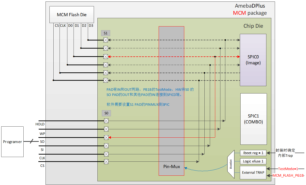
MCM Flash PG1B
Flash Probe Mode
In order to check the waveform of MCM Flash in case of Flash R/W error, 6 Flash pins (CS, CLK, D0~D3) should be connected out in debug mode.
Note
AmebaD只拉了4根pin出来,无法满足4IO的debug需求,因此AmebaDPlus需要把所有6根pin都拉出来。
MCM Flash Probe Mode
如果要观察MCM Flash的信号,则进入FLASH_PROBE_S1 Test Mode,此时可以检查SPIC到S1 Pad之间的波形

MCM flash FLASH_PROBE_S1 using pinmux path
Non-MCM Flash Probe Mode
如果要观察Non-MCM Flash的信号,则进入FLASH_PROBE_S0 Test Mode,此时可以检查SPIC到S1 Pad之间的波形

Non-MCM flash FLASH_PROBE_S0 using pinmux path
Non-MCM + MCM Flash Probe Mode

FLASH_PROBE_S0S1 using pinmux path
Packages
The package and Flash pinmux are listed in the following table.
Package |
Normal mode |
Normal mode |
Test mode |
|---|---|---|---|
Package |
MCM Flash |
Ext. Flash |
FT Test |
Non-MCM package |
S0 (4-bit) |
S0 (TEST_MODE == 0) |
|
MCM package |
S1 (4-bit) |
S0 (4-bit) |
S0 ((TEST_MODE == 1) && (ICFG = FORCE_USE_S0)) |
Timing Critical
Flash 正常read时,IO上的clock最快需要跑到100M+,但可以设置read latency 为1 or 2 cycle 或者 calibration ,program时,速度可以减低,比如20M,但一般是下降沿发,上升沿采,可以loop max delay可以设50ns。
flash device clk->do 约2~3ns (估计值,具体以flash spec为准)。
SPIC to/from PAD
SPIC作为master访问flash device时有以下几种case:
NON-MCM 接外部 flash,通过 S1 这组pad,read clock最高 100M+
MCM 接内部 flash,通过 S1 这组pad,read clock最高 100M+
MCM 时使用外部 flash,通过 S0这组pad,此时用于FT测试,速度可以适当降低
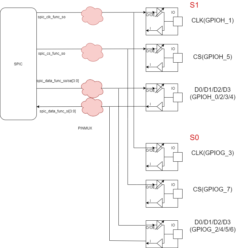
SPIC to/from PAD timing
需要设置 equal path 的有以下两组:
SPIC -> S1 pads , 包括path,skew要求较高,<1ns
spic_clk_func_so -> GPIOH_1
spic_cs_func_so -> GPIOH_5
spic_data_func_so/se -> GPIOH_0/2/3/4
SPIC -> S0 pads,包括以下path,skew 要求较低,<5ns
spic_clk_func_so -> GPIOG_3
spic_cs_func_so -> GPIOG_7
spic_data_func_so/se -> GPIOG_2/4/5/6
需要设置 max delay 的也是以下两组:
SPIC -> S1 pads + S1 pads -> SPIC 的 delay < 7ns (暂定,因为spic内部有calibraiton和read latency)
SPIC -> S0 pads + S0 pads -> SPIC 的 delay < 20ns (以20M 速度,falling打 rising采约束,总delay为25ns)
Flash PAD to/from PAD
使用外部PAD访问或debug flash时以下case
MCM-Flash 通过外部 PAD 进行 one-bit mode program,速度很低,可以估20M(TestMode13)
MCM-Flash 内部正常工作,通过外部pad进行逻辑时序监测 (TestMode15)
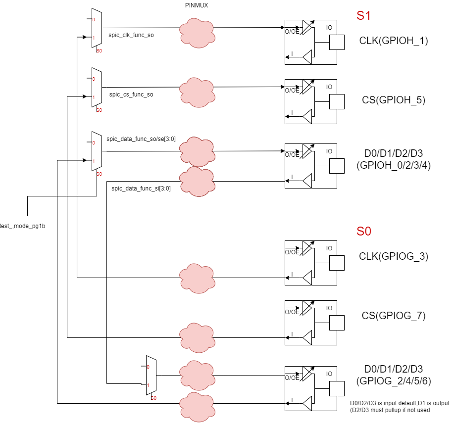
MCM-flash one-bit program (TESTMODE 13)
在 TestMode13下需要设置以下 equal path 和max delay
S0 pads -> S1 pads , 包括以下path,skew要求较低,<5ns
GPIOG_3 -> GPIOH_1
GPIOG_7 -> GPIOH_5
GPIOG_2/5/6 -> GPIOH_0/3/4
S0 pads -> S1 pads + S1 pads -> S0 pads < 20ns
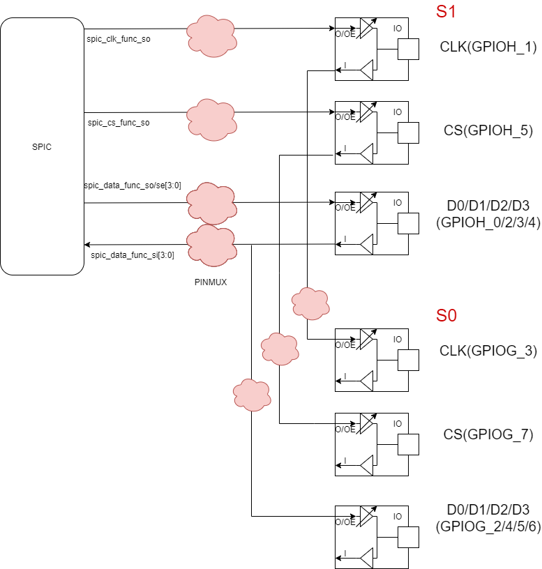
MCM-Flash dbg mode (TestMode 15)
在 TestMode15下需要设置以下 equal path ,max delay没有要求,因为都是同向输出。
S0 pads -> S1 pads , 包括以下path,skew要求较高,<1ns
GPIOH_1 -> GPIOG_3
GPIOH_5 -> GPIOG_7
GPIOH_0/2/3/4 -> GPIOG_2/4/5/6