Pseudo Static Random Access Memory (PSRAM)
Introduction
Application Scenario
The Random Access Memory (RAM) array uses dynamic cells that require periodic refresh. Refresh control logic within the device manages the refresh operations on the RAM array when the memory is not being actively read or written by the HyperBus interface master (Host). Since the host is not required to manage any refresh operations, the DRAM array appears to the host though the memory uses static cells that retain data without refresh. Hence, the memory can also be described as Pseudo Static RAM (PSRAM).
HyperBus is a Low Signal Count, Double Data Rate (DDR) interface that achieves high-speed read and write throughput. The DDR protocol transfers two data bytes per clock cycle on the DQ input/output signals.
As PSRAM can realize high-speed transmission of data stream, it is suitable for audio codec.
Features
Clock rata: 200MHz
Double Data Rate (DDR)
Read-Write Data Strobe (DQS)
Support Half sleep and deep power down mode
Programmable drive strength
Configurable refresh rate
Temperature Compensated Refresh
16/32/64/1024 bytes wrap burst access
Functional Description
Block Diagram
To communicate with PSRAM slave, PSRAM control unit is included in the system. It mainly includes two parts: PSRAM_LPC_CTRL and DDR PHY, as shown below.

PSRAM_LPC_CTRLis a slave device on AMBA-Bus system. It is used for data transmission and flow control.PSRAM_LPC_CTRLnow only supports DQ16 DDR PSRAM device (Low Pin Count PSRAM (LPC_PSRAM) or IO16PSRAM). There are two ports to accessPSRAM_LPC_CTRL:One is
AMBA-AXIinterface port, which is used for PSRAM data access.Another is
AMBA-APBinterface port, which is used for settingPSRAM_LPC_CTRLinternal control registers.
DDR PHYis used to provide correct data from PSRAM slave toPSRAM_LPC_CTRL. It contains a calibration circuit which is used to calibrate a stable data interval to access. PSRAM slave is an external memory device.
PSRAM Transaction
To communicate with PSRAM slave, PSRAM host must provide 20 bus signals, as shown below.
Chip Select (
CS#)Clock signal (
CK)Read Data Strobe (
DQS) or Data Mask(DM)16-bit data bus (
DQ[15:0])

For the host, DQS, or can be called DM, is used as Write Data Mask during write transactions, which is active high (DM = 1 means "do not write"). For the slave, DQS is used as Read Data Strobe during read transactions.
The internal logic of PSRAM slave is shown below.

PSRAM device signals are illustrated in following table. Active LOW signal symbol has a hash symbol (#) suffix.
Symbol |
Type |
Description |
|---|---|---|
CS# |
Host Output, Slave Input |
|
CK |
Host Output, Slave Input |
Clock signal: Command, address, and data information is output with respect to the crossing of the CK and CK# signals. Differential clock is used on 1.8V I/O devices. |
DQ[15:0] |
Input/Output |
Data Input/Output. Including command, address, and data. |
DQS/DM |
Input/Output |
Read-Write Data Strobe. DQ strobe clock during reads, Data mask during writes. DM is active high. DM = 1, means “do not write”. |
RESET# |
Host Output, Slave Input, Internal Pull-up |
Hardware RESET. When LOW the slave device, it will self initializes and returns to the Standby state. DQS/DM and DQ[15:0] are placed into the HI-Z state when RESET# is LOW. The slave RESET# input includes a weak pull-up. If RESET# is left unconnected, it will be pulled up to the HIGH state. |
Command/Address Bit Assignments
All HyperRAM bus transactions can be classified as either read or write. A bus transaction is started with CS# going LOW with clock in idle state (CK is LOW). The first three clock cycles transfer three words of Command/Address information to define the transaction characteristics. The Command/Address words are presented with DDR timing, using the rising and falling edges of the first three clocks.
The following characteristics are defined by the Command/Address information:
Read or Write transaction
Address Space: memory array space or register space
Register space is used to access device registers that identify the device characteristics and determine the slave specific behavior of read and write transfers on the HyperBus interface.
Whether a transaction will useing a linear or wrapped burst sequence.
The target row address (upper order address)
The target column (word within half-page) address (lower order address)
Note
The following figure shows the initial three clock cycles of all transactions on the HyperBus.
Command/Address information is center aligned with the clock during both read and write transactions.
Command/Address sequence
The following table lists the Command/Address bit assignment to DQ signals.
Command |
1st clock |
2nd clock |
2nd clock |
3rd clock |
3rd clock |
|---|---|---|---|---|---|
Sync Read |
00h |
A3 |
A2 |
A1 |
A0 |
Sync Write |
80h |
A3 |
A2 |
A1 |
A0 |
Sync Read (Linear Burst) |
20h |
A3 |
A2 |
A1 |
A0 |
Sync Write (Linear Burst) |
A0h |
A3 |
A2 |
A1 |
A0 |
Mode Register Read |
40h |
x |
x |
x |
MA |
Mode Register Write |
C0h |
x |
x |
x |
MA |
Global Reset |
FFh |
x |
x |
x |
x |
Note
x = don’t care.
A3 = unused address bits are reserved
A2 = 1’bx,
RA[12:6], unused address bit is reservedA1 =
RA[5:0], CA[9:8]A0 =
CA[7:0]MA = Mode register Address
The following table shows Memory space address map
Unit type |
Count |
Note |
|---|---|---|
Rows within 128Mb device |
16384 (rows) |
|
Row |
1 (row) |
512 (word addresses)/1K bytes |
Page |
1K bytes |
Note
Row numbers of different PSRAM devices are different.
A Row is a group of words relevant to the internal memory array structure. Also, the number of Rows may be used in the calculation of a distributed refresh interval for HyperRAM memory.
The Column address selects the burst transaction starting word location within a Row. The Column address is split into an upper and lower portion.
During wrapped transactions, access starts at the Command/Address selected location within the group, continues to the end of the configured word group aligned boundary, then wraps around to the beginning location in the group, then continues back to the starting location.
Read Transaction
The HyperBus master begins a transaction by driving CS# LOW while clock is idle. Then the clock begins toggling while Command/Address words are transferred.
Output Data is available after LC*2 latency cycles, which is defined in MR0 register of PSRAM.
Memory Read
The transaction of memory read is shown below.
New data is output edge aligned with every transition of DQS. Data will continues to be output as long as the host continues to transition the clock while CS# is LOW.
Register Read
Mode address in command determines which Mode register is read from as Data0, as shown below.
Write Transaction
The HyperBus master begins a transaction by driving CS# LOW while clock is idle. Then the clock begins toggling while CA words are transferred.
During the write data transfers, DQS/DM is driven by the host master interface as a data mask. When data is being written and DM is HIGH, the byte will be masked and the array will not be altered. When data is being written and DM is LOW, the data will be placed into the array.
Data will continues to be transferred as long as the HyperBus master continues to transition the clock while CS# is LOW. Write transfers can be ended at any time by bringing CS# HIGH when the clock is idle.
Memory Write
A minimum of 2 bytes (in X8 mode) / 2words (in X16 mode) of data must be input in a write operation. Single byte write operations can be performed by masking the un-written byte with DQS/DM, as shown below.
Write data is center aligned with the clock edges. The first byte of data in each word is captured by the memory on the rising edge of CK and the second byte is captured on the falling edge of CK.
Memory write transaction
Register Write
Register writes are latency 1, as shown below, whereas Register Reads uses the same latency settings in register MR0 of PSRAM.
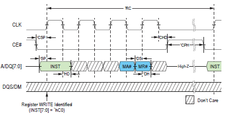
Register write transaction
PSRAM Controller Module
PSRAM Controller (PSRAMC) is used to communicate with PSRAM devices. To communicate with a PSRAM, it needs to set registers and transmit serial data to PSRAM . The series sequence steps are called user mode (user_mode). For users to control the PSRAMC easily, it supports automatic mode (auto_mode) to access PSRAM as accessing memory.
Configurable features:
FIFO depth- Configurable depth of FIFO from 1 to 256. The depth should not be smaller than the data bytes of the burst read.
TX_FIFO depth Extend- Configurable depth of
TX_FIFOfrom 1 to 256 and plus ExtendTX_FIFOentries. (These Extend Entries are for PSRAM to program command, address and etc.)
For more information about PSRAMC, refer to the chapter SPIC.
DDR PHY Module
DDR PHY module is designed as bridge between PSRAM CTRL and external PSRAM device. For host write, DDR PHY is as a simple path to transmit CA and data. When read from external PSRAM device, RWDS and DQ are aligned by edge. For internal timing, RWDS signal must be delayed for capturing DQ[15:0]. The data window for DQ is small, so the delay value must be adjusted according to the temperature or voltage variation. The calibration circuit is included to adjust the delay interval.
Calibration Function
After power on, software will calibrates a reliable N to make RWDS in DQ data window, and have a margin J. Every time a read burst happens, hardware will checks DQ at N-J, N, N+J three phases. Depending on the compare result, it will adjusts N or J after this read burst.
The following figure lists five cases of calibration function.
For case 2 and case 3, N will
-1or+1to left or right shift the data window.For case 5,
J--. When J becomes too small (reaches the Jmin), it will raises a calibration fail interrupt to CPU, telling software to do calibration again.When N is out of data window (as case 4) or data window becomes too small (
N - J < =0) before reading, it will also raises a calibration fail interrupt, and this time a more flag will be set to indicate that read data is wrong in statue register.If PHY do not receive RWDS within certain period, a timeout interrupt will be raised to CPU.

Calibration function cases
The calibration module contains 4 sub-modules, as shown below.
delay line: delay RWDS and generate
N-J,N,N+Jthree phase clockclk: control internal clocks
dchk: check data at three clock phases
ctrl: control adjust state machine

Calibration circuit diagram
Register
Psram Phy Register
Base Address: 0x40126000
Name
Address offset
Access
Description
000h
R/W
004h
R/W
008h
R/W
010h
R/W
018h
R/W
0F0h
R/W
0F8h
R
REG_CAL_CTRL
Size : 32
Address offset : 000h
Read/write access : R/W
Bit
Symbol
Access
Reset
Description
31:17
RSVD
R
-
Reserved
16
CFG_CAL_NBDR_OVF
R/W
0
The N reachs the boundary , which is 0 or Nmax .
Cleared by write 1 .
15
CFG_CAL_NBDR_ALMOST
R/W
0
The N-J or N+J reachs the boundary , which is 0 or Nmax .
Cleared by write 1 .
14
CFG_CAL_ERR_UNSURE
R/W
0
The Pre N/J may cause current burst receive error , but it is not sure because the burst len is too small.
Cleared by write 1 .
13
CFG_CAL_ERR_ALREADY
R/W
0
The Pre N/J may cause current burst receive error , even ch ange J to Jmin , the error still remain .
Cleared by write 1 .
12
CFG_CAL_ERR_ALMOST
R/W
0
The current burst receive correct , but next burst will set J = Jmin .
Cleared by write 1 .
11:9
RSVD
R
-
Reserved
8:4
CFG_CAL_INTR_MASK
R/W
5’b00011
Calibration fail interrupt mask , every bit control one even t above (1: enable , 0: disable)
[0] : err almost
[1] : err already
[2] : err unsure
[3] : nbdr almost
[4] : nbdr ovf
3:1
RSVD
R
-
Reserved
0
CFG_CAL_EN
R/W
1
Hardware auto calibration enable , if disable , N,J will be fixed .
REG_CAL_PAR
Size : 32
Address offset : 004h
Read/write access : R/W
Bit
Symbol
Access
Reset
Description
31:28
PRE_CAL_PHASE
R/W
4’h0
One-hot phase select, 4-tap delay line to adjust rwds phas e before calibration for large freq range or skew
Can be set to 0, bypassing the default 1-tap delay
27
RSVD
R
-
Reserved
26:24
CFG_CAL_JMIN
R/W
3’d2
Minimum J . Hardware may adjust J , if J reach this value , an interrup will be raised to alerm software.
23:20
RSVD
R
-
Reserved
19:16
CFG_CAL_JMAX
R/W
4’d14
Maximum J . Hardware may adjust J , but will not exceed this value.
15:12
RSVD
R
-
Reserved
11:8
CFG_CAL_J
R/W
4’d10
Initial value J calibrated by software .
7:5
RSVD
R
-
Reserved
4:0
CFG_CAL_N
R/W
5’d15
Initial value N calibrated by software .
REG_CAL_STATUS
Size : 32
Address offset : 008h
Read/write access : R/W
Bit
Symbol
Access
Reset
Description
31:29
RSVD
R
-
Reserved
28:24
CFG_CAL_CUR_ST
R/W
0
Calibration current state .
Cleared by write all 1 .
23:19
RSVD
R
-
Reserved
18:16
CFG_CAL_PDST
R/W
0
Calibration check result for last read burst .
[0] : indicate phase n+j , if 1 , means dn == dn+j
[1] : indicate phase n-j , if 1 , means dn == dn-j
[2] : if 1 , means the state is under j = jmin condition
15:12
RSVD
R
-
Reserved
11:8
CFG_CAL_CUR_J
R
0
Current value J read from hardware.
7:5
RSVD
R
-
Reserved
4:0
CFG_CAL_CUR_N
R
0
Current value N read from hardware.
REG_PHY_INFO
Size : 32
Address offset : 010h
Read/write access : R/W
Bit
Symbol
Access
Reset
Description
31:21
RSVD
R
-
Reserved
20
RX_TIME_OUT_MASK
R/W
1
Read time out interrupt mask
19:17
RSVD
R
-
Reserved
16
RX_TIME_OUT
R/W
0
Read time out interrupt if there’s no DQS/DQ from psram, wri te 1 to clear
15:8
RSVD
R
-
Reserved
7:0
CMD_INFO
R
8’h0
Command information, 1st Byte of Command/Address transaction
REG_PHY_CTRL
Size : 32
Address offset : 018h
Read/write access : R/W
Bit
Symbol
Access
Reset
Description
31
PSRAM_SW_RST_N
R/W
1’b1
Low active, except for phy register(using system reset), psr am software reset: psram, phy_ctrl, calibration
30:15
RSVD
R
-
Reserved
14
RWDS_CHK_OPT
R/W
1’b0
0: synced psram_rwds_i direct to controller
1: only check psram_rwds_i at last valid cycle of CA stage , sync this pulse to controller
13
RWDS_PD_EN
R/W
1’b0
Psram_phy can control PD pin of rwds iopad, bypass high-Z s tate at CMD/ADDR stage
12
LATENCY_TYPE
R/W
1’b0
Set this bit according to spic & psram latency settings
0: variable latency
1: fixed latency
11:8
RSVD
R
-
Reserved
7:4
CAL_RWDS_PHASE
R/W
4’h1
One-hot phase select, delay cal_rwds to push sampling data into rfifo
3:0
RFIFO_RDY_DLY
R/W
4’h0
Variable latency: delay read data cycles(phy clk) after dete cting first DQS rising edge, must < 4
Fixed latency: delay read data cycles(phy clk) after asserti ng spi_rx_data_en, must > 5
4*read_latency - rd_dummy_length + rfifo_rdy_dly = in_physi cal_cyc
REG_DBG_SEL
Size : 32
Address offset : 0F0h
Read/write access : R/W
Bit
Symbol
Access
Reset
Description
31:8
DUMMY
R/W
23’h0
7:0
PSRAM_PHY_DBG_SEL
R/W
8’h0
Psram phy debug select signal.
REG_DBG_INFO
Size : 32
Address offset : 0F8h
Read/write access : R
Bit
Symbol
Access
Reset
Description
31:0
PSRAM_PHY_DBG
R
32’h0
Psram phy debug signals.
Base Address: 0x41008000
Name
Address offset
Access
Description
000h
R/W
004h
R/W
008h
R/W
010h
R/W
018h
R/W
0F0h
R/W
0F8h
R
REG_CAL_CTRL
Size : 32
Address offset : 000h
Read/write access : R/W
Bit
Symbol
Access
Reset
Description
31:17
RSVD
R
-
Reserved
16
CFG_CAL_NBDR_OVF
R/W
0
The N reachs the boundary , which is 0 or Nmax .
Cleared by write 1 .
15
CFG_CAL_NBDR_ALMOST
R/W
0
The N-J or N+J reachs the boundary , which is 0 or Nmax .
Cleared by write 1 .
14
CFG_CAL_ERR_UNSURE
R/W
0
The Pre N/J may cause current burst receive error , but it is not sure because the burst len is too small.
Cleared by write 1 .
13
CFG_CAL_ERR_ALREADY
R/W
0
The Pre N/J may cause current burst receive error , even ch ange J to Jmin , the error still remain .
Cleared by write 1 .
12
CFG_CAL_ERR_ALMOST
R/W
0
The current burst receive correct , but next burst will set J = Jmin .
Cleared by write 1 .
11:9
RSVD
R
-
Reserved
8:4
CFG_CAL_INTR_MASK
R/W
5’b00011
Calibration fail interrupt mask , every bit control one even t above (1: enable , 0: disable)
[0] : err almost
[1] : err already
[2] : err unsure
[3] : nbdr almost
[4] : nbdr ovf
3:1
RSVD
R
-
Reserved
0
CFG_CAL_EN
R/W
1
Hardware auto calibration enable , if disable , N,J will be fixed .
REG_CAL_PAR
Size : 32
Address offset : 004h
Read/write access : R/W
Bit
Symbol
Access
Reset
Description
31:28
PRE_CAL_PHASE
R/W
4’h1
One-hot phase select, 4-tap delay line to adjust rwds phas e before calibration for large freq range or skew
Can be set to 0, bypassing the default 1-tap delay
27
RSVD
R
-
Reserved
26:24
CFG_CAL_JMIN
R/W
3’d2
Minimum J . Hardware may adjust J , if J reach this value , an interrup will be raised to alerm software.
23:20
RSVD
R
-
Reserved
19:16
CFG_CAL_JMAX
R/W
4’d14
Maximum J . Hardware may adjust J , but will not exceed this value.
15:12
RSVD
R
-
Reserved
11:8
CFG_CAL_J
R/W
4’d10
Initial value J calibrated by software .
7:5
RSVD
R
-
Reserved
4:0
CFG_CAL_N
R/W
5’d15
Initial value N calibrated by software .
REG_CAL_STATUS
Size : 32
Address offset : 008h
Read/write access : R/W
Bit
Symbol
Access
Reset
Description
31:29
RSVD
R
-
Reserved
28:24
CFG_CAL_CUR_ST
R/W
0
Calibration current state .
Cleared by write all 1 .
23:19
RSVD
R
-
Reserved
18:16
CFG_CAL_PDST
R/W
0
Calibration check result for last read burst .
[0] : indicate phase n+j , if 1 , means dn == dn+j
[1] : indicate phase n-j , if 1 , means dn == dn-j
[2] : if 1 , means the state is under j = jmin condition
15:12
RSVD
R
-
Reserved
11:8
CFG_CAL_CUR_J
R
0
Current value J read from hardware.
7:5
RSVD
R
-
Reserved
4:0
CFG_CAL_CUR_N
R
0
Current value N read from hardware.
REG_PHY_INFO
Size : 32
Address offset : 010h
Read/write access : R/W
Bit
Symbol
Access
Reset
Description
31:21
RSVD
R
-
Reserved
20
RX_TIME_OUT_MASK
R/W
1
Read time out interrupt mask
19:17
RSVD
R
-
Reserved
16
RX_TIME_OUT
R/W
0
Read time out interrupt if there’s no DQS/DQ from psram, wri te 1 to clear
15:8
RSVD
R
-
Reserved
7:0
CMD_INFO
R
8’h0
Command information, 1st Byte of Command/Address transaction
REG_PHY_CTRL
Size : 32
Address offset : 018h
Read/write access : R/W
Bit
Symbol
Access
Reset
Description
31
PSRAM_SW_RST_N
R/W
1’b1
Low active, except for phy register(using system reset), psr am software reset: psram, phy_ctrl, calibration
30:13
RSVD
R
-
Reserved
12
LATENCY_TYPE
R/W
1’b0
Set this bit according to spic & psram latency settings
0: variable latency
1: fixed latency
11:8
RSVD
R
-
Reserved
7:4
CAL_RWDS_PHASE
R/W
4’h1
One-hot phase select, delay cal_rwds to push sampling data into rfifo
3:0
RFIFO_RDY_DLY
R/W
4’h0
Variable latency: delay read data cycles(phy clk) after dete cting first DQS rising edge, must < 4
Fixed latency: delay read data cycles(phy clk) after asserti ng spi_rx_data_en, recommend 4 ~ 6
4*read_latency - rd_dummy_length + rfifo_rdy_dly = in_physi cal_cyc
REG_DBG_SEL
Size : 32
Address offset : 0F0h
Read/write access : R/W
Bit
Symbol
Access
Reset
Description
31
DUMMY
R/W
1’b0
ECO: option to mask 1T psram clk at the end of first rdata b lock
30:8
DUMMY
R/W
24’h0
7:0
PSRAM_PHY_DBG_SEL
R/W
8’h0
Psram phy debug select signal.
REG_DBG_INFO
Size : 32
Address offset : 0F8h
Read/write access : R
Bit
Symbol
Access
Reset
Description
31:0
PSRAM_PHY_DBG
R
32’h0
Psram phy debug signals.
Base Address: 0x41002000
Name
Address offset
Access
Description
000h
R/W
004h
R/W
008h
R/W
010h
R
018h
R/W
080h
R/W
084h
R/W
088h
R/W
08Ch
R/W
090h
R/W
094h
R/W
0F0h
R/W
0F8h
R
REG_CAL_CTRL
Size : 32
Address offset : 000h
Read/write access : R/W
Bit
Symbol
Access
Reset
Description
31:17
RSVD
R
-
Reserved
16
CFG_CAL_NBDR_OVF
R/W
0
The N reachs the boundary , which is 0 or Nmax .
Cleared by write 1 .
15
CFG_CAL_NBDR_ALMOST
R/W
0
The N-J or N+J reachs the boundary , which is 0 or Nmax .
Cleared by write 1 .
14
CFG_CAL_ERR_UNSURE
R/W
0
The Pre N/J may cause current burst receive error , but it is not sure because the burst len is too small.
Cleared by write 1 .
13
CFG_CAL_ERR_ALREADY
R/W
0
The Pre N/J may cause current burst receive error , even ch ange J to Jmin , the error still remain .
Cleared by write 1 .
12
CFG_CAL_ERR_ALMOST
R/W
0
The current burst receive correct , but next burst will set J = Jmin .
Cleared by write 1 .
11:9
RSVD
R
-
Reserved
8:4
CFG_CAL_INTR_MASK
R/W
5’b00011
Calibration fail interrupt mask , every bit control one even t above (1: enable , 0: disable)
[0] : err almost
[1] : err already
[2] : err unsure
[3] : nbdr almost
[4] : nbdr ovf
3:1
RSVD
R
-
Reserved
0
CFG_CAL_EN
R/W
1
Hardware auto calibration enable , if disable , N,J will be fixed .
REG_CAL_PAR
Size : 32
Address offset : 004h
Read/write access : R/W
Bit
Symbol
Access
Reset
Description
31:28
PRE_CAL_PHASE
R/W
4’h1
One-hot phase select, 4-tap delay line to adjust rwds phas e before calibration for large freq range or skew
Can be set to 0, bypassing the default 1-tap delay
27
RSVD
R
-
Reserved
26:24
CFG_CAL_JMIN
R/W
3’d2
Minimum J . Hardware may adjust J , if J reach this value , an interrup will be raised to alerm software.
23:20
RSVD
R
-
Reserved
19:16
CFG_CAL_JMAX
R/W
4’d14
Maximum J . Hardware may adjust J , but will not exceed this value.
15:12
RSVD
R
-
Reserved
11:8
CFG_CAL_J
R/W
4’d10
Initial value J calibrated by software .
7:5
RSVD
R
-
Reserved
4:0
CFG_CAL_N
R/W
5’d15
Initial value N calibrated by software .
REG_CAL_STATUS
Size : 32
Address offset : 008h
Read/write access : R/W
Bit
Symbol
Access
Reset
Description
31:29
RSVD
R
-
Reserved
28:24
CFG_CAL_CUR_ST
R/W
0
Calibration current state .
Cleared by write all 1 .
23:19
RSVD
R
-
Reserved
18:16
CFG_CAL_PDST
R/W
0
Calibration check result for last read burst .
[0] : indicate phase n+j , if 1 , means dn == dn+j
[1] : indicate phase n-j , if 1 , means dn == dn-j
[2] : if 1 , means the state is under j = jmin condition
15:12
RSVD
R
-
Reserved
11:8
CFG_CAL_CUR_J
R
0
Current value J read from hardware.
7:5
RSVD
R
-
Reserved
4:0
CFG_CAL_CUR_N
R
0
Current value N read from hardware.
REG_CMD_INFO
Size : 32
Address offset : 010h
Read/write access : R
Bit
Symbol
Access
Reset
Description
31:8
RSVD
R
-
Reserved
7:0
CMD_INFO
R
8’h0
Command information, 1st Byte of Command/Address transaction
REG_PHY_CTRL
Size : 32
Address offset : 018h
Read/write access : R/W
Bit
Symbol
Access
Reset
Description
31
PSRAM_SW_RST_N
R/W
1’b1
Low active, except for phy register(using system reset), psr am software reset: psram, phy_ctrl, calibration
30:12
RSVD
R
-
Reserved
11:9
CMD_END_DLY
R/W
3’h5
Delay required cycles(phy clk) after cmd end to bypass high-z DQS, must < (read_latency - 1)*2
8
CMD_RW_POL
R/W
1’b0
Polarity option for read/write bit in command, 0 for APM, 1 for winbond
7:4
CAL_RWDS_PHASE
R/W
4’h1
One-hot phase select, delay cal_rwds to push sampling data into rfifo
3:0
RFIFO_RDY_DLY
R/W
4’h6
Delay read data cycles(phy clk) from psram to controller, mu st >= 6
REG_DDR_PAD_CTRL0
Size : 32
Address offset : 080h
Read/write access : R/W
Bit
Symbol
Access
Reset
Description
31:27
RSVD
R
-
Reserved
26:0
DQ_CTRL_PSRAM
R/W
0x9a6
REG_DDR_PAD_CTRL1
Size : 32
Address offset : 084h
Read/write access : R/W
Bit
Symbol
Access
Reset
Description
31:14
RSVD
R
-
Reserved
13:8
DQ_TTCP_PSRAM
R/W
0
7:6
RSVD
R
-
Reserved
5:0
DQ_TTCN_PSRAM
R/W
0
REG_DDR_PAD_CTRL2
Size : 32
Address offset : 088h
Read/write access : R/W
Bit
Symbol
Access
Reset
Description
31:30
RSVD
R
-
Reserved
29:24
DQS_TTCN_PSRAM
R/W
0
23:22
RSVD
R
-
Reserved
21:16
DQS_TTCNB_PSRAM
R/W
0
15:14
RSVD
R
-
Reserved
13:8
DQS_TTCP_PSRAM
R/W
0
7:6
RSVD
R
-
Reserved
5:0
DQS_TTCPB_PSRAM
R/W
0
REG_DDR_PAD_CTRL3
Size : 32
Address offset : 08Ch
Read/write access : R/W
Bit
Symbol
Access
Reset
Description
31:12
RSVD
R
-
Reserved
11:0
DQS_N_CTRL_PSRAM
R/W
0x9a6
REG_DDR_PAD_CTRL4
Size : 32
Address offset : 090h
Read/write access : R/W
Bit
Symbol
Access
Reset
Description
31:28
RSVD
R
-
Reserved
27:0
DQS_P_CTRL_PSRAM
R/W
0x9a6
REG_DDR_PAD_CTRL5
Size : 32
Address offset : 094h
Read/write access : R/W
Bit
Symbol
Access
Reset
Description
31:22
RSVD
R
-
Reserved
21:16
VREF_S_0_PSRAM
R/W
0x2c
15:8
RD_PD_EN_DQ_PSRAM
R/W
0
7
RSVD
R
-
Reserved
6
REG_VREF_RANGE_SET_0_PSRAM
R/W
0x1
5
REG_VREF_PD_SET_0_PSRAM
R/W
0
4
REG_DDR2_MODE_PSRAM
R/W
0
3
RSVD
R
-
Reserved
2
RD_PD_EN_DM_PSRAM
R/W
0
1
RD_PD_EN_DQS_PSRAM
R/W
0
0
RD_ODT_EN_DQS_PSRAM
R/W
0
REG_DBG_SEL
Size : 32
Address offset : 0F0h
Read/write access : R/W
Bit
Symbol
Access
Reset
Description
31:8
RSVD
R
-
Reserved
7:0
PSRAM_PHY_DBG_SEL
R/W
8’h0
Psram phy debug select signal.
REG_DBG_INFO
Size : 32
Address offset : 0F8h
Read/write access : R
Bit
Symbol
Access
Reset
Description
31:0
PSRAM_PHY_DBG
R
32’h0
Psram phy debug signals.
Psram Controller Register
Base Address: 0x40127000
Name
Address offset
Access
Description
000h
R/W
It is used to setting related control in user mode. It can’t program when SSIENR is active.
004h
R/W
It is used to count a number of data frames of receiving data in user mode. If setting to 0, SPIC do esn’t receive any data in user mode. It can’t program when SSIENR is active.
008h
R/W
It is used to enable SPIC. If SSIENR is disabled, all transfers of user mode are halted and the user can’t program some control register if SSIENR is enabled.
Some bit fields of this register have different meaning at Read or Write operation. User should be c areful to control.
010h
R/W
It is used to select target SPI Flash in user mode. The user should be careful to program SER regist er. The contained value of SER should be a one-hot bit to select one Flash. It can’t program when S SIENR is active.
014h
R/W
It is used to configure spi_sclk. It is used in normal SPI command except fast read command. If BAUD R is setting 0 and executing the normal command, SPIC will halt in IDLE state. It can’t program when SSIENR is active.
018h
R/W
It causes to trigger a spi_txeir interrupt. It is used to control data flow for inform writing data into FIFO.
01Ch
R/W
It causes to trigger spi_rxfir interrupt. It is used to control data flow for inform reading serial data. It can’t program when SSIENR is active.
020h
R
It is used to inform the number of valid data entries in normal transfer except in receiving data. T hat is because FIFO is shared in transmit and receive mode. It can’t program when SSIENR is active.
024h
R
It is used to inform the number of valid data entries in receiving data.
028h
R/W
It is used to inform the status in transmitting or receiving operation.
02Ch
R/W
It is used to mask (disable) or enable all interrupts. When setting to 0, it would disable the speci fic interrupt. It can’t program when SSIENR is active.
030h
R
It is interrupt status register to indicate the interrupts status after masking.
034h
R
It is used to indicate the interrupt status prior to masking.
038h
R/W
It is used to clear spi_txoir_r interrupt.
03Ch
R/W
It is used to clear spi_rxoir_r interrupt.
040h
R/W
It is used to clear spi_rxuir_r interrupt.
044h
R/W
It is used to clear spi_mstir_r interrupt.
048h
R/W
It is used to clear all interrupt requests. When accessing the register, SPIC would set an active in terrupt to low.
04Ch
R/W
This register is only valid when SPIC is configured with a set of DMA Controller interface signals ( SPIFC_HAS_DMA = 1). When SPIC is not configured for DMA operation, this register will not exist and writing to the register’s address will have no effect; reading from this register address will retur n zero. It can’t program when SSIENR is active.
The register is used to enable the DMA Controller interface operation.
050h
R/W
This register is only valid when the SPIC is configured with a set of DMA interface signals (SPIFC_H AS_DMA = 1). When SPIC is not configured for DMA operation, this register will not exist and writing to its address will have no effect; reading from its address will return zero. It can’t program when SSIENR is active.
054h
R/W
This register is only valid when the SPIC is configured with a set of DMA interface signals (SPIFC_H AS_DMA = 1). When SPIC is not configured for DMA operation, this register will not exist and writing to its address will have no effect; reading from its address will return zero. It can’t program when SSIENR is active.
058h
R
It is read only register to define peripheral identification code of SPIC.
05Ch
R
It is read only register stores the SPIC version number.
060h
R/W
064h
R/W
068h
R/W
06Ch
R/W
070h
R/W
074h
R/W
078h
R/W
07Ch
R/W
080h
R/W
084h
R/W
088h
R/W
08Ch
R/W
090h
R/W
094h
R/W
098h
R/W
09Ch
R/W
0A0h
R/W
0A4h
R/W
0A8h
R/W
0ACh
R/W
0B0h
R/W
0B4h
R/W
0B8h
R/W
0BCh
R/W
0C0h
R/W
0C4h
R/W
0C8h
R/W
0CCh
R/W
0D0h
R/W
0D4h
R/W
0D8h
R/W
0DCh
R/W
0E0h
R/W
It is used to configure fast read command in auto mode. It can’t program when SSIENR is active.
0E4h
R/W
It is used to configure dual data read command in auto mode. It can’t program when SSIENR is active.
0E8h
R/W
It is used to configure the dual address and data read command in auto mode. It can’t program when S SIENR is active.
0ECh
R/W
It is used to configure quad data read command in auto mode. It can’t program when SSIENR is active.
0F0h
R/W
It is used to configure the quad address and data read command in auto mode. It can’t program when S SIENR is active.
0F4h
R/W
It is used to configure the single address and data write command in auto mode. It can’t program whe n SSIENR is active.
0F8h
R/W
It is used to configure dual data write command in auto mode. It can’t program when SSIENR is active .
0FCh
R/W
It is used to configure the dual address and data write command in auto mode. It can’t program when SSIENR is active.
100h
R/W
It is used to configure quad data write command in auto mode. It can’t program when SSIENR is active .
104h
R/W
It is used to configure the quad address and data write command in auto mode. It can’t program when SSIENR is active.
108h
R/W
It is used to configure write enable command before executing write command of auto mode. It can’t p rogram when SSIENR is active.
Available only if configuration of DDR_EN is defined
10Ch
R/W
It is used to implement read status command in auto mode. It can’t program when SSIENR is active.
110h
R/W
It is used to define SPIC hardware status. By programming the register, it is flexible to modify the fixed hardware. It can’t program when SSIENR is active.
114h
R/W
It is used to configure different baud rate to BAUDR register. It is for the fast read command. If F BAUDR is setting 0 and configure fast read command, SPIC will halt in IDLE state. It can’t program w hen SSIENR is active.
118h
R/W
It is used in user mode. It decides byte numbers of command, address and data phase to transmit. The address phase is between command phase and write/read data phase. For example, It may be address or data of writing status command… It can’t program when SSIENR is active.
11Ch
R/W
It decides the delay cycles to receive data in auto mode and a number of bytes address in read/write auto command. It can’t program when SSIENR is active.
120h
R/W
The register is used in auto mode. It decides the valid command to program/read SPI Flash. There are three parts to define auto mode including read command, write command and write control. In command parts, the user can indicate multiple valid commands of the target SPI Flash. SPIC would select the efficient one to execute the auto operation. If the user doesn’t define the valid commands in VALID_ CMD register, SPIC uses the single read and single write to execute.
In auto mode, SPIC can’t accept next operation until current operation is finishing completely. In a read operation, it is in the end when receiving corresponding data frames. In write data command, th e endpoint is determined WR_BLOCKING bit field. For efficient performance issue, the user can disabl e WR_BLOCKING to reducing writing cycles. But the user should ensure data coherence before reading d ata. In other words, if the user wants to ensure data is popped from FIFO, the user should enable WR _BLOCKING. It can’t program when SSIENR is active.
124h
R/W
The register is used in auto mode. It decides the shift numbers of address for decoding the target S PI Flash. The shift (auto mode) address is based on FLASH_MEM_BASE, so make sure you access the corr ect range. For optimization, the smallest flash size is 4KB and flash size should be an exponent of 2. It can’t program when SSIENR is active.
128h
R/W
The register is used to flush data and makes FIFO is empty. It’s usually using when there isn’t norm al operation in SPIC or data is crashed in FIFO.
12Ch
R/W
It is used to configure the dummy byte value, which is pushed after read address in auto mode. It ca n’t program when SSIENR is active.
130h
R/W
It is used to count a number of data frames of transmitting data in user mode. It can’t program when SSIENR is active.
134h
R/W
It is used to configure the SPI device information.
138h
R/W
Timing parameters of SPI devices.
13Ch
R/W
It decides the delay cycles to transmit data in auto mode. It can’t program when SSIENR is active.
140h
R/W
Timing parmeters of SPI device. It is used to configure the setup time relative to the spi_sclk. It can’t program when SSIENR is active.
180h
R
184h
R
188h
R
18Ch
R
190h
R
194h
R
198h
R
19Ch
R
1A0h
R
1A4h
R
1A8h
R
1ACh
R
1B0h
R
1B4h
R
1B8h
R
1BCh
R
1C0h
R
It is used to inform the number of valid data entries in status data.
1D0h
R/W
It is used to configure the page read command in auto mode. It can’t program when SSIENR is active.
REG_CTRLR0
Name : Control Register 0
Size : 32
Address offset : 000h
Read/write access : R/W
It is used to setting related control in user mode. It can’t program when SSIENR is active.
Bit
Symbol
Access
Reset
Description
31
USER_MODE
R/W
0x0
User mode bit. Enable to enter user mode. Disable to enter a uto mode. It can not be changed while SPIC is busy (0x28 [0] BUSY).
1: User mode. User can push data to FIFO and set SSIENR t o 1. SPIC won’t accept auto read/write command.
0: Auto mode. User can’t push data to FIFO and set SSIENR to 1. SPIC will accept auto read/write command.
30
UAR
R/W
0x0
User mode bit auto reset.
Enable to auto reset USER_MODE to 0 after current user mode transaction is over (SPIC_EN reset to 0).
29:28
RSVD
R
-
Reserved
27:23
CK_MTIMES
R/W
ATCK_MTIMES
Indicates the check times. If Flash is always busy in auto- check times, it causes ACEIR interrupt. The delay time (cycl es) is related to bus_clk.
The cycles of the parameter = (CK_MTIMES << (11+ATCK_BIT_EXT END).). User should ensure the timeout > Write time of Flash
The timeout time(ns) = 2*BAUDR*(1/SPIC_freq)(8/CH) (CK_MTIME S << (11+ATCK_BIT_EXTEND).)
Example 1: Flash Program time= 1ms, BAUDR=1, CH=1 (SPI) and (1/SPIC_freq) = 10ns. ATCK_MTIMES should be to set 4.
Example 2: SPIC_freq = 200MHz, BAUDR = 1, CH =4 (QSPI), and ATCK_BIT_EXTEND = 2, the maximum auto_check time should be
= 2*1*(1/200MHz)(8/4) (5’b11111<<13)
= 2*1*(1/200MHz)(8/4) (18’b11_1110_0000_0000_0000)
= 2*1*(1/200MHz)(8/4) (18’h3_e000)
= 2*1*(1/200MHz)(8/4) (253952)
= 5079040 ns
= 5.07 ms
Suggestion: If ACEIR interrupt occurs, the user should check the flash status by the software itself.
Note
Before SVN 8369 Version, CK_MTIMES is fixed to shift 10bi t. The formula becomes 2*BAUDR*(1/SPIC_freq)(8/CH) (CK_MT IMES << (10))
22
FAST_RD
R/W
0x0
Indicates to use fast read command in user mode. If setting to 1, SPIC would use FBAUDR to generate spi_sclk.
21:20
CMD_CH
R/W
0x0
Indicates channel number of command phase in transmitting or receiving data. Command phase is usually used to send SPI co mmand.
0: single channel
1: dual channels
2: quad channels
3: octal channel
19:18
DATA_CH
R/W
0x0
Indicates channel number of data phase in transmitting or re ceiving data. Data phase is used to send data after address phase.
0: single channel
1: dual channels
2: quad channels
3: octal channel
17:16
ADDR_CH
R/W
0x0
Indicates channel number of address phase after command phas e. Addr phase is used to send address or data. Addr phase is between one-byte command and a data phase. The number of by tes is determined by the ADDR_LENGTH.
0: single channel
1: dual channels
2: quad channels
3: octal channel
15:13
DDR_EN
R/W
0x0
Indicates the DDR mode in CMD_CH/DATA_CH/ADDR_CH.
CTRLR0[15]: CMD_CH (always 2-Byte CMD type)
CTRLR0[14]: DATA_CH
CTRLR0[13]: ADDR_CH
0: Disable
1: Enable
Note
Available only if configuration of DDR_EN is defined.
12
RSVD
R
-
Reserved
11
SPI_DREIR_R_DIS
R/W
0x0
Set to disable DR timeout check
10
GCLK_DIS
R/W
0x0
Set to disable gated clock of ICG cell
9:8
TMOD
R/W
0x0
Indicates transfer mode.
2’b00: transmit mode
Others (or 2’b11): receive mode
7
SCPOL
R/W
SCPOL_DEF
Indicates serial clock polarity. It is used to select the po larity of the inactive serial clock.
0: inactive state of serial clock is low
1: inactive state of serial clock is high
6
SCPH
R/W
SCPH_DEF
Indicates serial clock phase. The serial clock phase selects the relationship the serial clock with the slave select sign al.
0: serial clock toggles in middle of first data bit
1: serial clock toggles at start of first data bit
5
SIPOL_EN
R/W
0x0
Set to enable SIPOL
4:0
SIPOL
R/W
0x1F
While SIPOL_EN = 1:
SPI_CS is inactive state (SPI_CS ==1): spi_sin[3:0] = SIPOL[ 3:0]
SPI_CS is active (SPI_CS ==0): spi_sin[3:2] = SIPOL[3:2] (si ngle or dual channel)
(SIPOL[4]: reserved for spi_in[7:4])
REG_RX_NDF
Name : Control Register 1
Size : 32
Address offset : 004h
Read/write access : R/W
It is used to count a number of data frames of receiving data in user mode. If setting to 0, SPIC do
esn’t receive any data in user mode. It can’t program when SSIENR is active.
Bit
Symbol
Access
Reset
Description
31:24
RSVD
R
-
Reserved
23:0
RX_NDF
R/W
0x0
Indicates a number of data frames (unit: Byte).
When executing receives operation in user mode, SPIC receive s data continuously until data frames are equal to RX_NDF.
REG_SSIENR
Name : SPIC Enable Register
Size : 32
Address offset : 008h
Read/write access : R/W
It is used to enable SPIC. If SSIENR is disabled, all transfers of user mode are halted and the user
can’t program some control register if SSIENR is enabled.
Some bit fields of this register have different meaning at Read or Write operation. User should be c
areful to control.
Bit
Symbol
Access
Reset
Description
31:12
RSVD
R
-
Reserved
11:10
CUR_GP
R
0x0
Only used in frequency change function.
Used to identify which group register data is internal used. When frqc_req and frqc_ack are both high, CUR_GP will switch to the group which in GP_NUM.
9:8
GP_NUM
R/W
0x0
Only used in frequency change function.
Set to determine which group register user want to read or w rite. Base on different operation frequency, some control re gister setting will change.
Therefore we build second group register on USER_LENGTH.USER _RD_DUMMY_LENGTH, AUTO_LENGTH.RD_DUMMY_LENGTH, AUTO_LENGTH.R DSR_DUMMY_LENGTH, AUTO_LENGTH.IN_PHYSICAL_CYC, TPR0.CS_TCEM, TPR0.CS_ACTIVE_HOLD, TPR0.CS_H_WR_DUM_LEN, TPR0.CS_H_RD_DUM_ LEN, AUTO_LENGTH2.WR_DUMMY_LENGTH, TPR1.CR_TPWR, TPR1.CR_IDL E_WINDOW, TPR1.CS_ACTICE_SETUP.
7:5
RSVD
R
-
Reserved
4
PGM_RST_TEST_EN
R/W
0x0
For PGM RST Test only. Set this bit will generate a pulse as a warm reset signal and run PGM RST flow.
3
SREX
R/W
0x0
Set to block auto command before device can be normal access ed after exiting sleep mode.
This bit will hold high until timing check counter reaches t he set value in CTRLR0.CK_MTIMES.
2
FRQC
R/W
0x0
Set to enable frequency change function. SPIC will chop curr ent transaction and then set frqc_req = 1 after setting this bit. Frquency change is finished when frqc_req and frqc_ack are both high and then the choped transaction will return an d continue.
Write:
0: Not to activate FRQC
1: Activate FRQC
Read:
0: FRQC is still in progress
1: FRQC is done
1
ATCK_CMD
R/W
0x0
Set to enable ATCK_CMD implementation. After setting SPIC wo uld not accept any command until checking Flash is not busy or checking time out. (Use in User Mode, especially for Eras e/Program to check status automatically.)
If CTRLR2.SEQ_SET setting, this function needs to disable.
0
SPIC_EN
R/W
0x0
Set to enable SPIC and start user mode transaction.
SPIC will reset SPIC_EN to 0 after user mode transaction is finished.
SPIC_EN can only be set when BOOT_FIN=1 (boot finished) and USER_MODE=1 (user mode).
(User can read SPIC_EN to check whether current user mode tr ansaction is finished.)
REG_SER
Name : Slave Enable Register
Size : 32
Address offset : 010h
Read/write access : R/W
It is used to select target SPI Flash in user mode. The user should be careful to program SER regist
er. The contained value of SER should be a one-hot bit to select one Flash. It can’t program when S
SIENR is active.
Bit
Symbol
Access
Reset
Description
31:1
RSVD
R
-
Reserved
0
SER
R/W
0x1
Each bit in the register corresponds to one SPI Flash. In us er mode user program the register to select target flash.
0: Not selected
1: Selected
REG_BAUDR
Name : Baud Rate Select
Size : 32
Address offset : 014h
Read/write access : R/W
It is used to configure spi_sclk. It is used in normal SPI command except fast read command. If BAUD
R is setting 0 and executing the normal command, SPIC will halt in IDLE state. It can’t program when
SSIENR is active.
Bit
Symbol
Access
Reset
Description
31:12
RSVD
R
-
Reserved
11:0
SCKDV
R/W
Check SPIC frequency in configure form * *: (spic frequency) / 32 ex: spic freq=120 MHz, SCKDV= ⌊120/32⌋ = ⌊3.75⌋ =3
Define spi_sclk divider value.
The frequency of spi_sclk = The frequency of bus_clk / (2*SC KDV).
REG_TXFTLR
Name : Transmit FIFO Threshold level
Size : 32
Address offset : 018h
Read/write access : R/W
It causes to trigger a spi_txeir interrupt. It is used to control data flow for inform writing data
into FIFO.
Bit
Symbol
Access
Reset
Description
31:5
RSVD
R
-
Reserved
4:0
TFT
R/W
0x0
Transmit FIFO threshold. To Control FIFO entries of valid da ta in normal transfer except in receiving mode. When a numbe r of FIFO entry is equal or smaller than TFT, SPIC triggers a spi_txeir interrupt.
Ex: If TXFTLR = 5’h1, set spi_txeir when FIFO entries <= T FT (0x1)
REG_RXFTLR
Name : Receive FIFO Threshold level
Size : 32
Address offset : 01Ch
Read/write access : R/W
It causes to trigger spi_rxfir interrupt. It is used to control data flow for inform reading serial
data. It can’t program when SSIENR is active.
Bit
Symbol
Access
Reset
Description
31:5
RSVD
R
-
Reserved
4:0
RFT
R/W
{FIFO_ABW{1’b1}}
Receive FIFO threshold. To Control FIFO entries of valid dat a in receiving mode. When a number of FIFO entry is greater than RFT, SPIC triggers a spi_rxfir interrupt.
Ex: If RXFTLR = 5’h1, set spi_rxfir when FIFO entries > RF T (0x1)
REG_TXFLR
Name : Transmit FIFO level Register
Size : 32
Address offset : 020h
Read/write access : R
It is used to inform the number of valid data entries in normal transfer except in receiving data. T
hat is because FIFO is shared in transmit and receive mode. It can’t program when SSIENR is active.
Bit
Symbol
Access
Reset
Description
31:6
RSVD
R
-
Reserved
5:0
TXFLR
R
0x0
Transmit FIFO level. Indicates the FIFO entry level of valid data in normal mode except in receiving data. (or as FIFO_FL R in any mode)
REG_RXFLR
Name : Receive FIFO level Register
Size : 32
Address offset : 024h
Read/write access : R
It is used to inform the number of valid data entries in receiving data.
Bit
Symbol
Access
Reset
Description
31:6
RSVD
R
-
Reserved
5:0
RXFLR
R
0x0
Receive FIFO level. Indicates the FIFO entries of valid data in receiving data.
REG_SR
Name : Status Register
Size : 32
Address offset : 028h
Read/write access : R/W
It is used to inform the status in transmitting or receiving operation.
Bit
Symbol
Access
Reset
Description
31:9
RSVD
R
-
Reserved
8
ATWR_RDSR_N
R/W
0x0
The previous auto write cmd didn’t check the status register (RDSR). User should check the status register of Flash befor e next user mode transaction.
ATWR_RDSR_N will only be set by SPIC when SEQ_WR_EN = 1.
7
BOOT_FIN
R
0x0
(Not Yet Ready)
Boot Finish. Set if count waiting cycles (Boot Delay Count) for SPI Flash becomes a stable state after power on (or syst em reset). 1: Boot Finish
Note
Auto_mode would be blocked until boot finish. User_mode i s allowed with SSIENR inactive before boot finish.
6
DCOL
R
0x0
Data Collision, or in Transmitting Status.
1: Status shows that SPIC is transmitting spi_flash_cmd/sp i_flash_addr/spi_flash_data to SPI Flash.
Suggest not reading DR during this transmitting state. (Chec k this status can avoid reading wrong data and cause SPIC er ror.)
5
TXE
R
0x0
Transmission error. Set if FIFO is empty and starting to tra nsmit data to SPI Flash. This bit is cleared when read.
4
RFF
R
0x0
Receive FIFO full. Set if FIFO is full in receiving mode. Th is bit is cleared when read.
3
RFNE
R
0x0
Receive FIFO is not empty. Set if FIFO is not empty in recei ving mode. This bit is cleared when read.
2
TFE
R
0x1
Transmit FIFO is empty. Set if FIFO is empty in transmit mod e, else it is cleared when it has data in FIFO.
1
TFNF
R
0x1
Transmit FIFO is not full. Set if FIFO is not full in transm it mode, else it is cleared when FIFO is full.
0
BUSY
R
0x0
SPIC busy flag. Set if SPIC is still transmitting to or rece iving data from SPI Flash, or TX_FIFO/RX_FIFO are not empty.
REG_IMR
Name : Interrupt Mask Register
Size : 32
Address offset : 02Ch
Read/write access : R/W
It is used to mask (disable) or enable all interrupts. When setting to 0, it would disable the speci
fic interrupt. It can’t program when SSIENR is active.
Bit
Symbol
Access
Reset
Description
31:17
RSVD
R
-
Reserved
16
NWEIM
R/W
0x0
NAND Flash write error interrupt mask.
1: spi_nweir_r is not masked.
0: spi_nweir_r is masked.
Note
Available only if configuration of NAND_EN is defined.
15
STFIM
R/W
0x0
Status FIFO full interrupt mask.
1: spi_stfir is not masked.
0: spi_stfir is masked.
Note
Available only if configuration of NAND_EN is defined.
14
STOIM
R/W
0x0
Status FIFO overflow interrupt masked.
1: spi_stoir_r is not masked.
0: spi_stoir_r is masked.
Note
Available only if configuration of NAND_EN is defined.
13
STUIM
R/W
0x0
Status FIFO underflow interrupt masked.
1: spi_stuir_r is not masked.
0: spi_stuir_r is masked.
Note
Available only if configuration of NAND_EN is defined.
12
DREIM
R/W
0x0
DR timeout error interrupt mask.
1: spi_dreir_r is not masked.
0: spi_dreir_r is masked.
11
ACSIM
R/W
0x0
Auto-check Flash Status raw interrupt mask.
1: spi_acsir_r is not masked.
0: spi_acsis_r is masked.
10
TFSIM
R/W
0x0
Transmit finish interrupt mask.
1: spi_tfsir_r is not masked.
0: spi_tfsir_r is masked.
9
USEIM
R/W
0x0
User_mode error interrupt mask.
1: spi_useir_r is not masked.
0: spi_useir_r is masked.
8
ACEIM
R/W
0x1
Auto-check timeout error interrupt mask.
1: spi_aceir_r is not masked.
0: spi_aceir_r is masked.
7
BYEIM
R/W
0x1
The Byte-Enable error interrupt mask.
1: spi_byeir_r is not masked.
0: spi_byeir_r is masked.
6
WBEIM
R/W
0x1
Write burst error interrupt mask.
1: spi_wbier_r is not masked.
0: spi_wbeir_r is masked.
5
FSEIM
R/W
0x1
FIFO size error interrupt mask.
1: spi_fseir_r is not masked.
0: spi_fseir _r is masked
4
RXFIM
R/W
0x0
Receive FIFO full interrupt mask.
1: spi_rxfir is not masked.
0: spi_rxfir is masked.
3
RXOIM
R/W
0x1
Receive FIFO overflow interrupt masked.
1: spi_rxoir_r is not masked.
0: spi_rxoir_r is masked.
2
RXUIM
R/W
0x1
Receive FIFO underflow interrupt masked.
1: spi_rxuir_r is not masked.
0: spi_rxuir_r is masked.
1
TXOIM
R/W
0x1
Transmit FIFO overflow interrupt mask.
1: spi_txoir_r is not masked.
0: spi_txoir_r is masked.
0
TXEIM
R/W
0x0
Transmit FIFO empty interrupt masked.
1: spi_txeir is not masked.
0: spi_txeir is masked.
REG_ISR
Name : Interrupt Status Register
Size : 32
Address offset : 030h
Read/write access : R
It is interrupt status register to indicate the interrupts status after masking.
Bit
Symbol
Access
Reset
Description
31:17
RSVD
R
-
Reserved
16
NWEIS
R
0x0
NAND Flash write error interrupt status raw interrupt status after masking.
1: spi_nweir_r is active after masking.
0: spi_nweir_r is not active after masking.
Note
Available only if configuration of NAND_EN is defined.
15
STFIS
R
0x0
Status FIFO full raw interrupt status after masking.
1: spi_stfir_r is active after masking.
0: spi_stfir_r is not active after masking.
Note
Available only if configuration of NAND_EN is defined.
14
STOIS
R
0x0
Status FIFO overflow interrupt status after masking.
1: spi_stoir_r is active after masking.
0: spi_stoir_r is not active after masking.
Note
Available only if configuration of NAND_EN is defined.
13
STUIS
R
0x0
Status FIFO underflows interrupt status after masking.
1: spi_stuir_r is active after masking.
0: spi_stuir_r is not active after masking.
Note
Available only if configuration of NAND_EN is defined.
12
DREIS
R
0x0
DR timeout error status after masking.
1: spi_dreir_r is active after masking.
0: spi_dreir_r is not active after masking.
11
ACSIS
R
0x0
Auto-check Flash Status after masking.
1: spi_aceir_r is active after masking.
0: spi_aceir_r is not active after masking.
10
TFSIS
R
0x0
Transmit finish interrupt status after masking.
1: spi_tfsir_r is active after masking.
0: spi_tfsir_r is not active after masking.
9
USEIS
R
0x0
User mode error status after masking.
1: spi_useir_r is active after masking.
0: spi_useir_r is not active after masking.
8
ACEIS
R
0x0
Auto-check timeout error status after masking.
1: spi_aceir_r is active after masking.
0: spi_aceir_r is not active after masking.
7
BYEIS
R
0x0
The byte-Enable error interrupts status after masking.
1: spi_byeir_r is active after masking.
0: spi_byeir_r is not active after masking.
6
WBEIS
R
0x0
Write burst error interrupt status after masking.
1: spi_wbeir_r is active after masking.
0: spi_wbeir_r is not active after masking.
5
FSEIS
R
0x0
FIFO size error interrupts status after masking.
1: spi_fesir_r is active after masking.
0: spi_fesir_r is not active after masking.
4
RXFIS
R
0x0
Receive FIFO full interrupt status after masking
1: spi_rxfir is active after masking.
0: spi_rxfir is not active after masking.
3
RXOIS
R
0x0
Receive FIFO overflow interrupt status after masking.
1: spi_rxoir_r is active after masking.
0: spi_rxoir_r is not active after masking.
2
RXUIS
R
0x0
Receive FIFO underflows interrupt status after masking.
1: spi_rxuir_r is active after masking.
0: spi_rxuir_r is not active after masking.
1
TXOIS
R
0x0
Transmit FIFO overflow raw interrupt status after masking.
1: spi_txoir_r is active after masking.
0: spi_txoir_r is not active after masking.
0
TXEIS
R
0x0
Transmit FIFO empty raw interrupt status after masking.
1: spi_txeir is active after masking.
0: spi_txeir is not active after masking.
REG_RISR
Name : Raw Interrupt Status Register
Size : 32
Address offset : 034h
Read/write access : R
It is used to indicate the interrupt status prior to masking.
Bit
Symbol
Access
Reset
Description
31:17
RSVD
R
-
Reserved
16
NWEIR
R
0x0
NAND Flash write error interrupt status raw interrupt status prior to masking.
1: spi_nweir_r is active prior to masking.
0: spi_nweir_r is not active prior to masking.
Note
Available only if configuration of NAND_EN is defined.
15
STFIR
R
0x0
Status FIFO full raw interrupt status prior to masking
1: spi_stfir is active prior to masking.
0: spi_stfir is not active prior to masking.
Note
Available only if configuration of NAND_EN is defined.
14
STOIR
R
0x0
Status FIFO overflows raw interrupt status prior to masking.
1: spi_stoir_r is active prior to masking.
0: spi_stoir_r is not active prior to masking.
Note
Available only if configuration of NAND_EN is defined.
13
STUIR
R
0x0
Status FIFO underflows raw interrupt status prior to masking .
1: spi_stuir_r is active prior to masking.
0: spi_stuir_r is not active prior to masking.
Note
Available only if configuration of NAND_EN is defined.
12
DREIR
R
0x0
DR Timeout error status raw interrupt status prior to maskin g
1: spi_dreir_r is active prior to masking.
0: spi_dreir_r is not active prior to masking.
11
ACSIR
R
0x0
Auto-check Flash Status raw interrupt status prior to maski ng
1: spi_acsir_r is active prior to masking.
0: spi_acsir_r is not active prior to masking.
10
TFSIR
R
0x0
Transmit Finish Status raw interrupt status prior to masking
1: spi_tfsir_r is active prior to masking.
0: spi_tfsir_r is not active prior to masking.
9
USEIR
R
0x0
User_mode error status raw interrupt status prior to masking
1: spi_useir_r is active prior to masking.
0: spi_useir_r is not active prior to masking.
8
ACEIR
R
0x0
Auto-check timeout error status raw interrupt status prior to masking
1: spi_aceir_r is active prior to masking.
0: spi_aceir_r is not active prior to masking.
7
BYEIR
R
0x0
The Byte-Enable error interrupt status raw interrupt status prior to mask.
1: spi_byeir_r is active prior to masking.
0: spi_byeir_r is not active prior to masking.
6
WBEIR
R
0x0
Write burst error interrupt status raw interrupt status prio r to masking.
1: spi_wbeir_r is active prior to masking.
0: spi_wbeir_r is not active prior to masking.
5
FSEIR
R
0x0
FIFO size error interrupt status raw interrupt status prior to masking.
1: spi_fseir_r is active prior to masking.
0: spi_fseir _r is not active prior to masking.
4
RXFIR
R
0x0
Receive FIFO full raw interrupt status prior to masking
1:spi_rxfir is active prior to masking.
0: spi_rxfir is not active prior to masking.
3
RXOIR
R
0x0
Receive FIFO overflows raw interrupt status prior to masking .
1: spi_rxoir_r is active prior to masking.
0: spi_rxoir_r is not active prior to masking.
2
RXUIR
R
0x0
Receive FIFO underflows raw interrupt status prior to maskin g.
1: spi_rxuir_r is active prior to masking.
0: spi_rxuir_r is not active prior to masking.
1
TXOIR
R
0x0
Transmit FIFO overflow raw interrupt status prior to masking .
1: spi_txoir_r is active prior to masking.
0: spi_txoir_r is not active prior to masking.
0
TXEIR
R
0x0
Transmit FIFO empty raw interrupt status prior to masking.
1: spi_txeir is active prior to masking.
0: spi_txeir is not active prior to masking.
REG_TXOICR
Name : Transmit FIFO Overflow Interrupt Clear Register
Size : 32
Address offset : 038h
Read/write access : R/W
It is used to clear spi_txoir_r interrupt.
Bit
Symbol
Access
Reset
Description
31:1
RSVD
R
-
Reserved
0
TXOICR
R/W
0x0
When reading/writing the register, spi_rxoir_r would be clea red.
Note
Only response value 0x0 when read.
REG_RXOICR
Name : Receive FIFO Overflow Interrupt Clear Register
Size : 32
Address offset : 03Ch
Read/write access : R/W
It is used to clear spi_rxoir_r interrupt.
Bit
Symbol
Access
Reset
Description
31:1
RSVD
R
-
Reserved
0
RXOICR
R/W
0x0
When reading/writing the register, spi_rxoir_r would be clea red.
Note
Only response value 0x0 when read.
REG_RXUICR
Name : Receive FIFO Underflow Interrupt Clear Register
Size : 32
Address offset : 040h
Read/write access : R/W
It is used to clear spi_rxuir_r interrupt.
Bit
Symbol
Access
Reset
Description
31:1
RSVD
R
-
Reserved
0
RXUICR
R/W
0x0
When reading/writing the register, spi_rxuir_r would be clea red.
Note
Only response value 0x0 when read.
REG_MSTICR
Name : Master error Interrupt Clear Register
Size : 32
Address offset : 044h
Read/write access : R/W
It is used to clear spi_mstir_r interrupt.
Bit
Symbol
Access
Reset
Description
31:1
RSVD
R
-
Reserved
0
MSTICR
R/W
0x0
When reading/writing the register, spi_mstir_r would be clea red.
Note
Only response value 0x0 when read.
REG_ICR
Name : Interrupt Clear Register
Size : 32
Address offset : 048h
Read/write access : R/W
It is used to clear all interrupt requests. When accessing the register, SPIC would set an active in
terrupt to low.
Bit
Symbol
Access
Reset
Description
31:1
RSVD
R
-
Reserved
0
ICR
R/W
0x0
When reading/writing the register, all interrupt would be cl eared.
Note
Only response value 0x0 when read.
REG_DMACR
Name : DMA Control Register
Size : 32
Address offset : 04Ch
Read/write access : R/W
This register is only valid when SPIC is configured with a set of DMA Controller interface signals (
SPIFC_HAS_DMA = 1). When SPIC is not configured for DMA operation, this register will not exist and
writing to the register’s address will have no effect; reading from this register address will retur
n zero. It can’t program when SSIENR is active.
The register is used to enable the DMA Controller interface operation.
Bit
Symbol
Access
Reset
Description
31:2
RSVD
R
-
Reserved
1
TX_DMAC_EN
R/W
0x0
Transmit DMA Enable. This bit enables/disables the transmit FIFO DMA channel.
0: Transmit DMA disabled
1: Transmit DMA enabled
0
RX_DMAC_EN
R/W
0x0
Receive DMA Enable. This bit enables/disables the receive FI FO DMA channel
0: Receive DMA disabled
1: Receive DMA enabled
REG_DMATDLR
Name : DMA Transmit Data Level Register
Size : 32
Address offset : 050h
Read/write access : R/W
This register is only valid when the SPIC is configured with a set of DMA interface signals (SPIFC_H
AS_DMA = 1). When SPIC is not configured for DMA operation, this register will not exist and writing
to its address will have no effect; reading from its address will return zero. It can’t program when
SSIENR is active.
Bit
Symbol
Access
Reset
Description
31:5
RSVD
R
-
Reserved
4:0
DMATDL
R/W
0x0
Transmit Data Level. This bit field controls the level at wh ich a DMA request is made by the transmit logic. It is equal to the watermark level; that is, the dma_tx_req signal is ge nerated when the number of valid data entries in the transmi t FIFO is equal to or below this field value, and TDMAE = 1.
REG_DMARDLR
Name : DMA Receive Data Level Register
Size : 32
Address offset : 054h
Read/write access : R/W
This register is only valid when the SPIC is configured with a set of DMA interface signals (SPIFC_H
AS_DMA = 1). When SPIC is not configured for DMA operation, this register will not exist and writing
to its address will have no effect; reading from its address will return zero. It can’t program when
SSIENR is active.
Bit
Symbol
Access
Reset
Description
31:5
RSVD
R
-
Reserved
4:0
DMARDL
R/W
0x0
Receive Data Level. This bit field controls the level at whi ch a DMA request is made by the receive logic. The watermark level = DMARDL+1; that is, dma_rx_req is generated when the number of valid data entries in the receive FIFO is equal to or above this field value + 1, and RDMAE=1.
REG_IDR
Name : Identification Register
Size : 32
Address offset : 058h
Read/write access : R
It is read only register to define peripheral identification code of SPIC.
Bit
Symbol
Access
Reset
Description
31:0
IDCODE
R
{16’h CR_version, 16’hFF01} e.g., if there are two SPICs in a chip, the ID should be 0x0203_FF01 for #1 SPIC v2.3 and 0x0203_FF02 for #2 SPIC v2.3
Contain the decimal value of SPIC version.
REG_SPIC_VERSION
Name : SPIC version ID Register
Size : 32
Address offset : 05Ch
Read/write access : R
It is read only register stores the SPIC version number.
Bit
Symbol
Access
Reset
Description
31:0
SPIC_VERSION
R
{16’d SVN_NUM, 16’d Encryptd_Date} SVN_NUM: version of SPIC rtl design Encrypted_Date: generated date
Contain the decimal value of SPIC version.
(After 201612: SVN_NUM changes to Git Counter)
REG_DR0
Name : Data Register 0
Size : 32
Address offset : 060h
Read/write access : R/W
Bit
Symbol
Access
Reset
Description
31:0
DR0
R/W
0x0
It is a data buffer with 8-bit width FIFO. If accessing in word data byte, it would read/write 4 entries of FIFO.
REG_DR1
Name : Data Register 1
Size : 32
Address offset : 064h
Read/write access : R/W
Bit
Symbol
Access
Reset
Description
31:0
DR1
R/W
0x0
It is a data buffer with 8-bit width FIFO. If accessing in word data byte, it would read/write 4 entries of FIFO.
REG_DR2
Name : Data Register 2
Size : 32
Address offset : 068h
Read/write access : R/W
Bit
Symbol
Access
Reset
Description
31:0
DR2
R/W
0x0
It is a data buffer with 8-bit width FIFO. If accessing in word data byte, it would read/write 4 entries of FIFO.
REG_DR3
Name : Data Register 3
Size : 32
Address offset : 06Ch
Read/write access : R/W
Bit
Symbol
Access
Reset
Description
31:0
DR3
R/W
0x0
It is a data buffer with 8-bit width FIFO. If accessing in word data byte, it would read/write 4 entries of FIFO.
REG_DR4
Name : Data Register 4
Size : 32
Address offset : 070h
Read/write access : R/W
Bit
Symbol
Access
Reset
Description
31:0
DR4
R/W
0x0
It is a data buffer with 8-bit width FIFO. If accessing in word data byte, it would read/write 4 entries of FIFO.
REG_DR5
Name : Data Register 5
Size : 32
Address offset : 074h
Read/write access : R/W
Bit
Symbol
Access
Reset
Description
31:0
DR5
R/W
0x0
It is a data buffer with 8-bit width FIFO. If accessing in word data byte, it would read/write 4 entries of FIFO.
REG_DR6
Name : Data Register 6
Size : 32
Address offset : 078h
Read/write access : R/W
Bit
Symbol
Access
Reset
Description
31:0
DR6
R/W
0x0
It is a data buffer with 8-bit width FIFO. If accessing in word data byte, it would read/write 4 entries of FIFO.
REG_DR7
Name : Data Register 7
Size : 32
Address offset : 07Ch
Read/write access : R/W
Bit
Symbol
Access
Reset
Description
31:0
DR7
R/W
0x0
It is a data buffer with 8-bit width FIFO. If accessing in word data byte, it would read/write 4 entries of FIFO.
REG_DR8
Name : Data Register 8
Size : 32
Address offset : 080h
Read/write access : R/W
Bit
Symbol
Access
Reset
Description
31:0
DR8
R/W
0x0
It is a data buffer with 8-bit width FIFO. If accessing in word data byte, it would read/write 4 entries of FIFO.
REG_DR9
Name : Data Register 9
Size : 32
Address offset : 084h
Read/write access : R/W
Bit
Symbol
Access
Reset
Description
31:0
DR9
R/W
0x0
It is a data buffer with 8-bit width FIFO. If accessing in word data byte, it would read/write 4 entries of FIFO.
REG_DR10
Name : Data Register 10
Size : 32
Address offset : 088h
Read/write access : R/W
Bit
Symbol
Access
Reset
Description
31:0
DR10
R/W
0x0
It is a data buffer with 8-bit width FIFO. If accessing in word data byte, it would read/write 4 entries of FIFO.
REG_DR11
Name : Data Register 11
Size : 32
Address offset : 08Ch
Read/write access : R/W
Bit
Symbol
Access
Reset
Description
31:0
DR11
R/W
0x0
It is a data buffer with 8-bit width FIFO. If accessing in word data byte, it would read/write 4 entries of FIFO.
REG_DR12
Name : Data Register 12
Size : 32
Address offset : 090h
Read/write access : R/W
Bit
Symbol
Access
Reset
Description
31:0
DR12
R/W
0x0
It is a data buffer with 8-bit width FIFO. If accessing in word data byte, it would read/write 4 entries of FIFO.
REG_DR13
Name : Data Register 13
Size : 32
Address offset : 094h
Read/write access : R/W
Bit
Symbol
Access
Reset
Description
31:0
DR13
R/W
0x0
It is a data buffer with 8-bit width FIFO. If accessing in word data byte, it would read/write 4 entries of FIFO.
REG_DR14
Name : Data Register 14
Size : 32
Address offset : 098h
Read/write access : R/W
Bit
Symbol
Access
Reset
Description
31:0
DR14
R/W
0x0
It is a data buffer with 8-bit width FIFO. If accessing in word data byte, it would read/write 4 entries of FIFO.
REG_DR15
Name : Data Register 15
Size : 32
Address offset : 09Ch
Read/write access : R/W
Bit
Symbol
Access
Reset
Description
31:0
DR15
R/W
0x0
It is a data buffer with 8-bit width FIFO. If accessing in word data byte, it would read/write 4 entries of FIFO.
REG_DM_DR0
Name : Data Mask Data Register 0
Size : 32
Address offset : 0A0h
Read/write access : R/W
Bit
Symbol
Access
Reset
Description
31:2
RSVD
R
-
Reserved
1
DATA_EN_DR0
R/W
0x0
It is a data buffer for spi_data_en signal in user mode. The output value of spi_data_en is the data that has been pushed to DM_FIFO [1]. If DM_FIFO is empty, the output value of spi _data_en will be 0.
0
DATA_MASK_DR0
R/W
0x0
It is a data buffer for spi_dm signal in user mode. The outp ut value of spi_dm is the data that has been pushed to DM_FI FO [0]. If DM_FIFO is empty, the output value of spi_data_en will be (~DM_ACT).
REG_DM_DR1
Name : Data Mask Data Register 1
Size : 32
Address offset : 0A4h
Read/write access : R/W
Bit
Symbol
Access
Reset
Description
31:2
RSVD
R
-
Reserved
1
DATA_EN_DR1
R/W
0x0
It is a data buffer for spi_data_en signal in user mode. The output value of spi_data_en is the data that has been pushed to DM_FIFO [1]. If DM_FIFO is empty, the output value of spi _data_en will be 0.
0
DATA_MASK_DR1
R/W
0x0
It is a data buffer for spi_dm signal in user mode. The outp ut value of spi_dm is the data that has been pushed to DM_FI FO [0]. If DM_FIFO is empty, the output value of spi_data_en will be (~DM_ACT).
REG_DM_DR2
Name : Data Mask Data Register 2
Size : 32
Address offset : 0A8h
Read/write access : R/W
Bit
Symbol
Access
Reset
Description
31:2
RSVD
R
-
Reserved
1
DATA_EN_DR2
R/W
0x0
It is a data buffer for spi_data_en signal in user mode. The output value of spi_data_en is the data that has been pushed to DM_FIFO [1]. If DM_FIFO is empty, the output value of spi _data_en will be 0.
0
DATA_MASK_DR2
R/W
0x0
It is a data buffer for spi_dm signal in user mode. The outp ut value of spi_dm is the data that has been pushed to DM_FI FO [0]. If DM_FIFO is empty, the output value of spi_data_en will be (~DM_ACT).
REG_DM_DR3
Name : Data Mask Data Register 3
Size : 32
Address offset : 0ACh
Read/write access : R/W
Bit
Symbol
Access
Reset
Description
31:2
RSVD
R
-
Reserved
1
DATA_EN_DR3
R/W
0x0
It is a data buffer for spi_data_en signal in user mode. The output value of spi_data_en is the data that has been pushed to DM_FIFO [1]. If DM_FIFO is empty, the output value of spi _data_en will be 0.
0
DATA_MASK_DR3
R/W
0x0
It is a data buffer for spi_dm signal in user mode. The outp ut value of spi_dm is the data that has been pushed to DM_FI FO [0]. If DM_FIFO is empty, the output value of spi_data_en will be (~DM_ACT).
REG_DM_DR4
Name : Data Mask Data Register 4
Size : 32
Address offset : 0B0h
Read/write access : R/W
Bit
Symbol
Access
Reset
Description
31:2
RSVD
R
-
Reserved
1
DATA_EN_DR4
R/W
0x0
It is a data buffer for spi_data_en signal in user mode. The output value of spi_data_en is the data that has been pushed to DM_FIFO [1]. If DM_FIFO is empty, the output value of spi _data_en will be 0.
0
DATA_MASK_DR4
R/W
0x0
It is a data buffer for spi_dm signal in user mode. The outp ut value of spi_dm is the data that has been pushed to DM_FI FO [0]. If DM_FIFO is empty, the output value of spi_data_en will be (~DM_ACT).
REG_DM_DR5
Name : Data Mask Data Register 5
Size : 32
Address offset : 0B4h
Read/write access : R/W
Bit
Symbol
Access
Reset
Description
31:2
RSVD
R
-
Reserved
1
DATA_EN_DR5
R/W
0x0
It is a data buffer for spi_data_en signal in user mode. The output value of spi_data_en is the data that has been pushed to DM_FIFO [1]. If DM_FIFO is empty, the output value of spi _data_en will be 0.
0
DATA_MASK_DR5
R/W
0x0
It is a data buffer for spi_dm signal in user mode. The outp ut value of spi_dm is the data that has been pushed to DM_FI FO [0]. If DM_FIFO is empty, the output value of spi_data_en will be (~DM_ACT).
REG_DM_DR6
Name : Data Mask Data Register 6
Size : 32
Address offset : 0B8h
Read/write access : R/W
Bit
Symbol
Access
Reset
Description
31:2
RSVD
R
-
Reserved
1
DATA_EN_DR6
R/W
0x0
It is a data buffer for spi_data_en signal in user mode. The output value of spi_data_en is the data that has been pushed to DM_FIFO [1]. If DM_FIFO is empty, the output value of spi _data_en will be 0.
0
DATA_MASK_DR6
R/W
0x0
It is a data buffer for spi_dm signal in user mode. The outp ut value of spi_dm is the data that has been pushed to DM_FI FO [0]. If DM_FIFO is empty, the output value of spi_data_en will be (~DM_ACT).
REG_DM_DR7
Name : Data Mask Data Register 7
Size : 32
Address offset : 0BCh
Read/write access : R/W
Bit
Symbol
Access
Reset
Description
31:2
RSVD
R
-
Reserved
1
DATA_EN_DR7
R/W
0x0
It is a data buffer for spi_data_en signal in user mode. The output value of spi_data_en is the data that has been pushed to DM_FIFO [1]. If DM_FIFO is empty, the output value of spi _data_en will be 0.
0
DATA_MASK_DR7
R/W
0x0
It is a data buffer for spi_dm signal in user mode. The outp ut value of spi_dm is the data that has been pushed to DM_FI FO [0]. If DM_FIFO is empty, the output value of spi_data_en will be (~DM_ACT).
REG_DM_DR8
Name : Data Mask Data Register 8
Size : 32
Address offset : 0C0h
Read/write access : R/W
Bit
Symbol
Access
Reset
Description
31:2
RSVD
R
-
Reserved
1
DATA_EN_DR8
R/W
0x0
It is a data buffer for spi_data_en signal in user mode. The output value of spi_data_en is the data that has been pushed to DM_FIFO [1]. If DM_FIFO is empty, the output value of spi _data_en will be 0.
0
DATA_MASK_DR8
R/W
0x0
It is a data buffer for spi_dm signal in user mode. The outp ut value of spi_dm is the data that has been pushed to DM_FI FO [0]. If DM_FIFO is empty, the output value of spi_data_en will be (~DM_ACT).
REG_DM_DR9
Name : Data Mask Data Register 9
Size : 32
Address offset : 0C4h
Read/write access : R/W
Bit
Symbol
Access
Reset
Description
31:2
RSVD
R
-
Reserved
1
DATA_EN_DR9
R/W
0x0
It is a data buffer for spi_data_en signal in user mode. The output value of spi_data_en is the data that has been pushed to DM_FIFO [1]. If DM_FIFO is empty, the output value of spi _data_en will be 0.
0
DATA_MASK_DR9
R/W
0x0
It is a data buffer for spi_dm signal in user mode. The outp ut value of spi_dm is the data that has been pushed to DM_FI FO [0]. If DM_FIFO is empty, the output value of spi_data_en will be (~DM_ACT).
REG_DM_DR10
Name : Data Mask Data Register 10
Size : 32
Address offset : 0C8h
Read/write access : R/W
Bit
Symbol
Access
Reset
Description
31:2
RSVD
R
-
Reserved
1
DATA_EN_DR10
R/W
0x0
It is a data buffer for spi_data_en signal in user mode. The output value of spi_data_en is the data that has been pushed to DM_FIFO [1]. If DM_FIFO is empty, the output value of spi _data_en will be 0.
0
DATA_MASK_DR10
R/W
0x0
It is a data buffer for spi_dm signal in user mode. The outp ut value of spi_dm is the data that has been pushed to DM_FI FO [0]. If DM_FIFO is empty, the output value of spi_data_en will be (~DM_ACT).
REG_DM_DR11
Name : Data Mask Data Register 11
Size : 32
Address offset : 0CCh
Read/write access : R/W
Bit
Symbol
Access
Reset
Description
31:2
RSVD
R
-
Reserved
1
DATA_EN_DR11
R/W
0x0
It is a data buffer for spi_data_en signal in user mode. The output value of spi_data_en is the data that has been pushed to DM_FIFO [1]. If DM_FIFO is empty, the output value of spi _data_en will be 0.
0
DATA_MASK_DR11
R/W
0x0
It is a data buffer for spi_dm signal in user mode. The outp ut value of spi_dm is the data that has been pushed to DM_FI FO [0]. If DM_FIFO is empty, the output value of spi_data_en will be (~DM_ACT).
REG_DM_DR12
Name : Data Mask Data Register 12
Size : 32
Address offset : 0D0h
Read/write access : R/W
Bit
Symbol
Access
Reset
Description
31:2
RSVD
R
-
Reserved
1
DATA_EN_DR12
R/W
0x0
It is a data buffer for spi_data_en signal in user mode. The output value of spi_data_en is the data that has been pushed to DM_FIFO [1]. If DM_FIFO is empty, the output value of spi _data_en will be 0.
0
DATA_MASK_DR12
R/W
0x0
It is a data buffer for spi_dm signal in user mode. The outp ut value of spi_dm is the data that has been pushed to DM_FI FO [0]. If DM_FIFO is empty, the output value of spi_data_en will be (~DM_ACT).
REG_DM_DR13
Name : Data Mask Data Register 13
Size : 32
Address offset : 0D4h
Read/write access : R/W
Bit
Symbol
Access
Reset
Description
31:2
RSVD
R
-
Reserved
1
DATA_EN_DR13
R/W
0x0
It is a data buffer for spi_data_en signal in user mode. The output value of spi_data_en is the data that has been pushed to DM_FIFO [1]. If DM_FIFO is empty, the output value of spi _data_en will be 0.
0
DATA_MASK_DR13
R/W
0x0
It is a data buffer for spi_dm signal in user mode. The outp ut value of spi_dm is the data that has been pushed to DM_FI FO [0]. If DM_FIFO is empty, the output value of spi_data_en will be (~DM_ACT).
REG_DM_DR14
Name : Data Mask Data Register 14
Size : 32
Address offset : 0D8h
Read/write access : R/W
Bit
Symbol
Access
Reset
Description
31:2
RSVD
R
-
Reserved
1
DATA_EN_DR14
R/W
0x0
It is a data buffer for spi_data_en signal in user mode. The output value of spi_data_en is the data that has been pushed to DM_FIFO [1]. If DM_FIFO is empty, the output value of spi _data_en will be 0.
0
DATA_MASK_DR14
R/W
0x0
It is a data buffer for spi_dm signal in user mode. The outp ut value of spi_dm is the data that has been pushed to DM_FI FO [0]. If DM_FIFO is empty, the output value of spi_data_en will be (~DM_ACT).
REG_DM_DR15
Name : Data Mask Data Register 15
Size : 32
Address offset : 0DCh
Read/write access : R/W
Bit
Symbol
Access
Reset
Description
31:2
RSVD
R
-
Reserved
1
DATA_EN_DR15
R/W
0x0
It is a data buffer for spi_data_en signal in user mode. The output value of spi_data_en is the data that has been pushed to DM_FIFO [1]. If DM_FIFO is empty, the output value of spi _data_en will be 0.
0
DATA_MASK_DR15
R/W
0x0
It is a data buffer for spi_dm signal in user mode. The outp ut value of spi_dm is the data that has been pushed to DM_FI FO [0]. If DM_FIFO is empty, the output value of spi_data_en will be (~DM_ACT).
REG_READ_FAST_SINGLE
Name : Fast Read Data Command of SPI Flash
Size : 32
Address offset : 0E0h
Read/write access : R/W
It is used to configure fast read command in auto mode. It can’t program when SSIENR is active.
Bit
Symbol
Access
Reset
Description
31:16
RSVD
R
-
Reserved
15:0
FRD_CMD
R/W
0x0B0B
Indicate SPI Flash command value of fast read command. The b aud rate is used with FBAUDR.
FRD_CMD[15:8] is for RD_OCTA_IO_CMD_2nd_BYTE (only available when configuration of DDR_EN is defined)
FRD_CMD[7:0] is for RD_OCTA_IO_CMD_1st_BYTE
REG_READ_DUAL_DATA
Name : Dual Output Read Command of SPI Flash
Size : 32
Address offset : 0E4h
Read/write access : R/W
It is used to configure dual data read command in auto mode. It can’t program when SSIENR is active.
Bit
Symbol
Access
Reset
Description
31:8
RSVD
R
-
Reserved
7:0
RD_DUAL_O_CMD
R/W
0x3B
Indicates SPI Flash command value of dual data read command.
REG_READ_DUAL_ADDR_DATA
Name : Dual I/O Read Command of SPI Flash
Size : 32
Address offset : 0E8h
Read/write access : R/W
It is used to configure the dual address and data read command in auto mode. It can’t program when S
SIENR is active.
Bit
Symbol
Access
Reset
Description
31:8
RSVD
R
-
Reserved
7:0
RD_DUAL_IO_CMD
R/W
0xBB
Indicates SPI Flash command value of dual address and data r ead command.
REG_READ_QUAD_DATA
Name : Qaud Output Read Command of SPI Flash
Size : 32
Address offset : 0ECh
Read/write access : R/W
It is used to configure quad data read command in auto mode. It can’t program when SSIENR is active.
Bit
Symbol
Access
Reset
Description
31:8
RSVD
R
-
Reserved
7:0
RD_QUAD_O_CMD
R/W
0x6B
Indicates SPI Flash command value of quad data read command.
REG_READ_QUAD_ADDR_DATA
Name : Quad I/O Read Command of SPI Flash
Size : 32
Address offset : 0F0h
Read/write access : R/W
It is used to configure the quad address and data read command in auto mode. It can’t program when S
SIENR is active.
Bit
Symbol
Access
Reset
Description
31:24
EXIT_PRM_CMD
R/W
0xFF
Exit High Performance Read Mode commend.
Note
Available only if configuration of PRM_EN is defined (SPI C Lite ver).
23:16
PRM_VAL
R/W
0xA5
High Performance Read Mode Value.
Note
Available only if configuration of PRM_EN is defined (SPI C Lite ver).
15:8
EXIT_PRM_DUM_LEN
R/W
0x0
If Exit PRM commend is more than 1 byte, use EXIT_PRM_DUM_LE N to extend the commend. It is referenced by bus_clk.
Ex. In qpi mode (4-4-4), FFFFFFFFh data cycle should be is sued (4-byte data in 8 spi cycles). EXIT_PRM_CMD only push 1 byte (2 spi cycles), so use EXIT_PRM_DUM_LEN to extend 6 s pi cycles.
EXIT_PRM_DUM_LEN = 6 (spi_cycle) * (2 * baurd_rate)
Note
Available only if configuration of PRM_EN is defined (SPI C Lite ver).
7:0
RD_QUAD_IO_CMD
R/W
0xEB
Indicates SPI Flash command value of quad address and data r ead command.
REG_WRITE_SIGNLE
Name : Page Program Command of SPI Flash
Size : 32
Address offset : 0F4h
Read/write access : R/W
It is used to configure the single address and data write command in auto mode. It can’t program whe
n SSIENR is active.
Bit
Symbol
Access
Reset
Description
31:16
RSVD
R
-
Reserved
15:0
WR_CMD
R/W
0x0202
Indicate SPI Flash command value of write command.
WR_CMD[15:8] is for WR_OCTA_IO_CMD_2nd_BYTE (only available when configuration of DDR_EN is defined)
WR_CMD[7:0] is for WR_OCTA_IO_CMD_1st_BYTE
REG_WRITE_DUAL_DATA
Name : Dual Data Input Program Command of SPI Flash
Size : 32
Address offset : 0F8h
Read/write access : R/W
It is used to configure dual data write command in auto mode. It can’t program when SSIENR is active
.
Bit
Symbol
Access
Reset
Description
31:8
RSVD
R
-
Reserved
7:0
WR_DUAL_I_CMD
R/W
0xA2
Indicates SPI Flash command value of dual data write command .
REG_WRITE_DUAL_ADDR_DATA
Name : Dual Address and Data Output Read Command of SPI Flash
Size : 32
Address offset : 0FCh
Read/write access : R/W
It is used to configure the dual address and data write command in auto mode. It can’t program when
SSIENR is active.
Bit
Symbol
Access
Reset
Description
31:8
RSVD
R
-
Reserved
7:0
WR_DUAL_II_CMD
R/W
0x0
Indicates SPI Flash command value of dual address and data w rite command.
REG_WRITE_QUAD_DATA
Name : Quad Data Input Program Command of SPI Flash
Size : 32
Address offset : 100h
Read/write access : R/W
It is used to configure quad data write command in auto mode. It can’t program when SSIENR is active
.
Bit
Symbol
Access
Reset
Description
31:8
RSVD
R
-
Reserved
7:0
WR_QUAD_I_CMD
R/W
0x32
Indicates SPI Flash command value of quad data write command .
REG_WRITE_QUAD_ADDR_DATA
Name : Quad Address and Data Output Read Command of SPI Flash
Size : 32
Address offset : 104h
Read/write access : R/W
It is used to configure the quad address and data write command in auto mode. It can’t program when
SSIENR is active.
Bit
Symbol
Access
Reset
Description
31:8
RSVD
R
-
Reserved
7:0
WR_QUAD_II_CMD
R/W
0x38
Indicates SPI Flash command value of quad address and data w rite command.
REG_WRITE_ENABLE
Name : Write Enable Command of SPI Flash
Size : 32
Address offset : 108h
Read/write access : R/W
It is used to configure write enable command before executing write command of auto mode. It can’t p
rogram when SSIENR is active.
Available only if configuration of DDR_EN is defined
Bit
Symbol
Access
Reset
Description
31:16
RSVD
R
-
Reserved
15:8
WR_EN_CMD_2ND_BYTE
R/W
0x06
Indicates SPI Flash command value of 2nd byte of write enabl e.
Note
Available only if configuration of DDR_EN is defined.
7:0
WR_EN_CMD_1ST_BYTE
R/W
0x06
Indicates SPI Flash command value of 1st byte of write enabl e.
REG_READ_STATUS
Name : Read Status Command of SPI Flash
Size : 32
Address offset : 10Ch
Read/write access : R/W
It is used to implement read status command in auto mode. It can’t program when SSIENR is active.
Bit
Symbol
Access
Reset
Description
31
INTERVAL_EN
R/W
0x0
Set to enable INTERVAL_ODD.
Note
Available only if configuration of SPIC_LITE is not defin ed (SPIC Full ver).
30
INTERVAL_ODD
R/W
0x0
Indicates SPI Flash read status with 2-Byte status but chec king only odd byte or even byte.
0: even byte (2, 4, 6, ...)
1: odd byte (1, 3, 5, ...)
Note
Available only if configuration of SPIC_LITE is not defin ed (SPIC Full ver).
29:28
ST_CMD_LEN
R/W
0x1
Indicates the number of bytes in read status command.
ST_CMD_LEN can be 1~3.
Note
Available only if configuration of SPIC_LITE is not defin ed (SPIC Full ver).
27:26
ST_CMD_CH
R/W
0x0
Indicates channel number of read status command in transmitt ing and receiving data.
0: single channel
1: dual channels
2: quad channels
3: octal channel
25
ST_CMD_DDR_EN
R/W
0x0
Indicates the DDR mode in ST_CMD_CH.
Note
Available only if configuration of DDR_EN is defined.
24
RSVD
R
-
Reserved
23:16
RD_ST_CMD_3RD_BYTE
R/W
0x00
Indicates SPI Flash command value of 3rd byte of read status .
Note
Available only if configuration of SPIC_LITE is not defin ed (SPIC Full ver).
15:8
RD_ST_CMD_2ND_BYTE
R/W
0x05
Indicates SPI Flash command value of 2nd byte of read status .
Note
Available only if configuration of SPIC_LITE is not defin ed (SPIC Full ver).
7:0
RD_ST_CMD_1ST_BYTE
R/W
0x05
Indicates SPI Flash command value of 1st byte of read status .
REG_CTRLR2
Name : Control Register 2
Size : 32
Address offset : 110h
Read/write access : R/W
It is used to define SPIC hardware status. By programming the register, it is flexible to modify the
fixed hardware. It can’t program when SSIENR is active.
Bit
Symbol
Access
Reset
Description
31:24
RSVD
R
-
Reserved
23:19
RD_WEIGHT
R/W
0x2
Set to determine the read and write priority. RD_WEIGHT shou ld >= 2 (if set to 0 or 1, RD_WEIGHT will use the previous v alue).
Ex: if RD_WEIGHT = 5, SPIC will accept 1 write cmd after a ccepting 4 read cmd.
18
RSVD
R
-
Reserved
17
WR_VL_EN
R/W
0x0
Set to enable variable write latency. SPIC will set variable write latency according to RWDS.
If WR_VL_EN = 0, SPIC will set fix write latency.
16
RD_VALID_EN
R/W
0x0
Set to enable variable read latency. SPIC will not sample re ad data until rx_data_valid = 1.
If RD_VALID_EN = 0, SPIC will sample read data according to internal counter.
15
DIS_WRAP_ALIGN
R/W
0x0
Set to disable wrap_align function (convert wrap to incremen tal through aligning start address to burst boundary) in aut o mode.
If DIS_WRAP_ALIGN = 1, SPIC will chop wrap transation into t wo incremental transactions.
14
DIS_DM_CA
R/W
0x0
Set to disable spi_dm_oe_n (let the device to drive DM) when SPIC pushing CMD and ADDR for both user mode and auto mode.
13
FULL_WR
R/W
0x1
Set to enable full write in auto mode.
If FULL_WR = 0, SPIC will use spi_dm to do the partial write .
Note
Available only if configuration of DM_EN is defined.
12
DM_ACT
R/W
0x1
DM (Data Mask) is active high or low, which is defined by sp ecific PSRAM SPEC.
If DM is active high (DM=1 means “don’t write”), DM_ACT shou ld be set to 1 and the corresponding byte of write data will not be written into the PSRAM.
Note
Available only if configuration of DM_EN is defined.
11:8
RX_FIFO_ENTRY
R/W
0x5
If using SPIC_HAS_DMA (NO_MERGE_FIFO) SPIC, this field indic ates the valid entry of RX FIFO. It is an index of 2 and it should be equal or smaller than 5. The user can modify it to profile with a different entry.
Ex: if RX_FIFO entry is 32, RX_FIFO_ENTYR <=5.
7:4
TX_FIFO_ENTRY
R/W
FIFO_ABW
If using SPIC_HAS_DMA (NO_MERGE_FIFO) SPIC, this field indic ates the valid entry of TX_FIFO. If using MERGE_FIFO SPIC, t here is only one FIFO is in the SPIC design, and this field indicates the valid entry of the FIFO. It is an index of 2 a nd it should be equal or smaller than FIFO_ABW. The user can modify it to profile with a different entry.
Ex: if FIFO entry is 32, FIFO_ENTYR <=5.
3
DR_FIXED
R/W
0x0
Indicate the AXI FIXED read mode on DR.
If setting 1, user mode read DR will be FIXED.
Otherwise, user mode read DR will be INCR.
2
WPN_DNUM
R/W
0
Indicates the WPn input pin of SPI Flash is connected to spi _sout[2]or [3].
If setting 0, it connects to spi_sdata[2]. Otherwise, it con nects to spi_sdata[3].
1
WPN_SET
R/W
0
To implement write protect function. spi_wen_out and the bit of spi_sout which connects to WPN would be initial to 0.
WPN_SET: If setting 1 is protected. Otherwise, is not protec ted.(Configuration Form is using “WPN_SET_n”: If setting 1 i s NOT protected. Otherwise, is protected.)
0
SO_DNUM
R/W
1
Indicates SO input pin of SPI Flash is connected to spi_sout [0]or [1]. It refers to SPI Flash and also the system connec tion with SPI_Flash (see 6.1.3)
If setting 0, it connects to spi_sout[0] (single-channel co nnection).
Otherwise, it connects to spi_sout[1] (multi-channels conne ction).
(Default is configured to 1to support multi-channel connect ion)
REG_FBAUDR
Name : Fast Baud Rate Select
Size : 32
Address offset : 114h
Read/write access : R/W
It is used to configure different baud rate to BAUDR register. It is for the fast read command. If F
BAUDR is setting 0 and configure fast read command, SPIC will halt in IDLE state. It can’t program w
hen SSIENR is active.
Bit
Symbol
Access
Reset
Description
31:12
RSVD
R
-
Reserved
11:0
FSCKDV
R/W
0x01
Indicates the divider of Fast read command when FAST_RD is s etting in user mode or using fast read command in auto mode. The frequency of spi_sclk is derived from:
Frequency of spi_sclk = Frequency of bus_clk / (2*FSCKDV).
REG_USER_LENGTH
Name : User Length Register
Size : 32
Address offset : 118h
Read/write access : R/W
It is used in user mode. It decides byte numbers of command, address and data phase to transmit. The
address phase is between command phase and write/read data phase. For example, It may be address or
data of writing status command… It can’t program when SSIENR is active.
Bit
Symbol
Access
Reset
Description
31:20
RSVD
R
-
Reserved
19:16
USER_ADDR_LENGTH
R/W
0x3
Indicates number of bytes in address phase (between command phase and write/read phase) in user mode.
If it is set to 4, it will transmit 4-byte Address to suppo rt 4-byte address mode in SPI Flash.
15:14
RSVD
R
-
Reserved
13:12
USER_CMD_LENGHT
R/W
0x0
Indicates number of bytes in command phase in user mode.
USER_CMD_LENGHT can be 0~3.
11:0
USER_RD_DUMMY_LENGTH
R/W
0x0
Indicates delay cycles for receiving data in user mode (USER _MODE == 1).
It is referenced by bus_clk.
REG_AUTO_LENGTH
Name : Auto Address Length Register
Size : 32
Address offset : 11Ch
Read/write access : R/W
It decides the delay cycles to receive data in auto mode and a number of bytes address in read/write
auto command. It can’t program when SSIENR is active.
Bit
Symbol
Access
Reset
Description
31:28
RSVD
R
-
Reserved
27:20
RDSR_DUMMY_LENGTH
R/W
0x0
Indicates delay cycles for receiving data after Read Status Register (RDSR) command. (auto write or user mode with auto check)
It is referenced by bus_clk.
19:16
AUTO_ADDR_LENGTH
R/W
FLASH_ADDR_BYTE
Indicates number of bytes address in read/write command in a uto mode.
AUTO_ADDR_LENGTH should be 1, 2, 3, 4 bytes.
If it is set to 4, it will transmit 4-byte Address to suppo rt 4-byte address mode in SPI Flash.
Note
PRM in auto mode should set VALID_CMD[11] (PRM_EN) with c orrect AUTO_ADDR_LENGTH.
15:12
IN_PHYSICAL_CYC
R/W
0x0
Indicates how many SPIC CLK (bus_clk) cycles from pad to int ernal SPIC.
11:0
RD_DUMMY_LENGTH
R/W
DUMMY_CYCLE
Indicates delay cycles for receiving data.
It is referenced by bus_clk.
Note
Don’t include SPIC CLK (bus_clk) cycles from pad to inter nal SPIC
REG_VALID_CMD
Name : Valid Command Register
Size : 32
Address offset : 120h
Read/write access : R/W
The register is used in auto mode. It decides the valid command to program/read SPI Flash. There are
three parts to define auto mode including read command, write command and write control. In command
parts, the user can indicate multiple valid commands of the target SPI Flash. SPIC would select the
efficient one to execute the auto operation. If the user doesn’t define the valid commands in VALID_
CMD register, SPIC uses the single read and single write to execute.
In auto mode, SPIC can’t accept next operation until current operation is finishing completely. In a
read operation, it is in the end when receiving corresponding data frames. In write data command, th
e endpoint is determined WR_BLOCKING bit field. For efficient performance issue, the user can disabl
e WR_BLOCKING to reducing writing cycles. But the user should ensure data coherence before reading d
ata. In other words, if the user wants to ensure data is popped from FIFO, the user should enable WR
_BLOCKING. It can’t program when SSIENR is active.
Bit
Symbol
Access
Reset
Description
31:16
RSVD
R
-
Reserved
15
SEQ_WR_EN
R/W
0x0
Set (1) to enable read sequential transaction write function in auto mode. If two bus write transactions are sequential ( address is consecutive), SPIC can access second transaction data without sending Read CMD/ADDR/DUMMY.
Once disable (0) this bit field, spi_csn will inactive immed iately and also disable this function.
Note
Run SEQ_WR_EN after SPIC boot finish.
14
SEQ_RD_EN
R/W
0x1
Set (1) to enable read sequential transaction read function in auto mode. If two bus read transactions are sequential (a ddress is consecutive), SPIC can access second transaction d ata without sending Read CMD/ADDR/DUMMY.
Once disable (0) this bit field, spi_csn will inactive immed iately and also disable this function.
Note
Run SEQ_RD_EN after SPIC boot finish.
13
DUM_EN
R/W
0x0
Enable to push one dummy byte (DUM_BYTE_VAL) after pushing a ddress to Flash in auto read. If PRM_EN is active, it will p ush PRM_Value instead of DUM_BYTE_VAL.
If RD_DUMMY_LENGTH = 0, it won’t push the dummy byte.
12
CTRLR0_CH
R/W
0x0
Set (1) to use CTRLR0 CMD_CH/DATA_CH/ADDR_CH and DDR_EN fiel d in Auto mode; Otherwise, SPIC will decode according to whi ch VALID_CMD you choose in auto mode.
Suggestion while use this bit field:
Read Flash mode: (1-4-8), (4-4-8), (1-4D-8D), (4-4D- 8D) with using RD_QUAD_IO[7:0]
Read Flash mode (with 2-Byte CMD): (1-8-8), (8-8-8), (8 D-8D-8D), (4D-4D-4D) with using RD_FAST_SINGLE_IO[15:0] (always using FBAUD)
Write Flash mode: (1-4-8), (4-4-8) with using WR_QUAD_IO [7:0]
Write Flash mode (with 2-Byte CMD): (1-8-8), (8-8-8), ( 8D-8D-8D) with using WR_SINGLE_IO[15:0]
11
PRM_EN
R/W
0x0
Set to enable SPIC performance read mode in Auto Mode. RXI- 312 SPIC will auto exit performance read mode before auto wr ite or enter to user mode.
Enter PRM Flow:
Set CR_VALID_CMD[11] (PRM_EN) with CR_VALID_CMD[4] (RD_QUAD_ IO) or with (CR_VALID_CMD[0] and CR_VALID_CMD[12])
Set CR_READ_QUAD_ADDR_DATA[23:16] (PRM_VALUE) and [7:0] (RD_ QUAD_IO_CMD)
Set correct Dummy Cycle, and Valid Command then access in Au to Mode address range
If PRM_EN, at 1st time Auto Rd, it will access with CMD, and store this condition. At 2nd Auto Rd or later, it will acces s without CMD but with Address and Mode Value. Our SPIC will check PRM_VALUE (CR_READ_QUAD_ADDR_DATA [23:16]), if PRM_VAL UE ==0x00 (not a valid PRM value), and PRM_EN is set, SPIC w ill always access SPI Flash with (CMD+ADDR+MODE+DUMMY+…) f ormat.
10
RM_WEN
R/W
0x0
Remove write enable command in auto write.
9
RM_RDSR
R/W
0x0
Remove read status register in auto write.
8
WR_QUAD_II
R/W
VALID_CMD_DEF[8]
Indicates quad address/data write is a valid command to exec ute. (known as (1-4-4))
7
WR_QUAD_I
R/W
VALID_CMD_DEF[7]
Indicates quad data write is a valid command to execute. (kn own as (1-1-4))
6
WR_DUAL_II
R/W
VALID_CMD_DEF[6]
Indicates dual address/data write is a valid command to exec ute. (known as (1-2-2))
5
WR_DUAL_I
R/W
VALID_CMD_DEF[5]
Indicates dual data write is a valid command to execute. (kn own as (1-1-2))
4
RD_QUAD_IO
R/W
VALID_CMD_DEF[4]
Indicates quad address/data read is a valid command to execu te. (known as (1-4-4))
3
RD_QUAD_O
R/W
VALID_CMD_DEF[3]
Indicates quad data read is a valid command to execute. (kno wn as (1-1-4))
2
RD_DUAL_IO
R/W
VALID_CMD_DEF[2]
Indicates dual address/data read is a valid command to execu te. (known as (1-2-2))
1
RD_DUAL_I
R/W
VALID_CMD_DEF[1]
Indicates dual data read is a valid command to execute. (kno wn as (1-1-2))
0
FRD_SINGLE
R/W
VALID_CMD_DEF[0]
Indicates fast read command is a valid command to execute. ( known as (1-1-1))
REG_FLASE_SIZE
Name : Flash Size Register
Size : 32
Address offset : 124h
Read/write access : R/W
The register is used in auto mode. It decides the shift numbers of address for decoding the target S
PI Flash. The shift (auto mode) address is based on FLASH_MEM_BASE, so make sure you access the corr
ect range. For optimization, the smallest flash size is 4KB and flash size should be an exponent of
It can’t program when SSIENR is active.
Bit
Symbol
Access
Reset
Description
31:5
RSVD
R
-
Reserved
4:0
FLASH_SIZE
R/W
FLASH_MEM_SIZE - 12
Indicates the size of flash to select the target SPI Flash i n auto mode. The number is an exponent of 2 (Flash size) -1 2 (the smallest flash size is 4kB).
Ex: If flash size is 4MB (22-bit), set FLASH_SIZE = 10 (2 2-12).
REG_FLUSH_FIFO
Name : Flush FIFO Register
Size : 32
Address offset : 128h
Read/write access : R/W
The register is used to flush data and makes FIFO is empty. It’s usually using when there isn’t norm
al operation in SPIC or data is crashed in FIFO.
Bit
Symbol
Access
Reset
Description
31:3
RSVD
R
-
Reserved
2
FLUSH_ST_FIFO
R/W
0x0
Clear all data in the ST_FIFO when writing to FLUSH_ST_FIFO register.
1
FLUSH_DR_FIFO
R/W
0x0
Clear all data in the TX_FIFO and RX_FIFO when writing to FL USH_DR_FIFOregister.
0
FLUSH_ALL
R/W
0x0
Clear all data in all FIFO (include TX_FIFO, RX_FIFO and ST_ FIFO) and reset all FSM when writing to FLUSH_ALL register.
REG_DUM_BYTE
Name : Dummy byte value
Size : 32
Address offset : 12Ch
Read/write access : R/W
It is used to configure the dummy byte value, which is pushed after read address in auto mode. It ca
n’t program when SSIENR is active.
Bit
Symbol
Access
Reset
Description
31:8
RSVD
R
-
Reserved
7:0
DUM_BYTE_VAL
R/W
0x00
Push dummy byte value.
REG_TX_NDF
Name : TX_NDF
Size : 32
Address offset : 130h
Read/write access : R/W
It is used to count a number of data frames of transmitting data in user mode. It can’t program when
SSIENR is active.
Bit
Symbol
Access
Reset
Description
31:24
RSVD
R
-
Reserved
23:0
TX_NDF
R/W
0x00
Indicates a number of data frames (Unit: Byte). After transm itting command and address, SPIC transmits data continuously until data frames are equal to TX_NDF. TX_NDF can set larger than TX_FIFO size.
REG_DEVICE_INFO
Name : Device info
Size : 32
Address offset : 134h
Read/write access : R/W
It is used to configure the SPI device information.
Bit
Symbol
Access
Reset
Description
31:15
RSVD
R
-
Reserved
14
DATA_UNIT_4B
R/W
0x0
Set (1) when the SPI device stores 4-byte data for each add ress.
13
DQ16_DATA_CH
R/W
0x0
Set (1) when DQ16 PSRAM uses 16-bit data channel.
When DQ16_DATA_CH = 1’b1, set CTRLR0[19:18] DATA_CH = 2’b00.
12
DATA_UNIT_2B
R/W
0x0
Set (1) when the SPI device stores 2-byte data for each add ress.
Note
Available only if configuration of PSRAM_EN is defined.
11
JEDEC_P2CMF
R/W
0x0
Set (1) when the SPI cmd is JEDEC Profile 2.0 Command Modifi er Formats. (6-byte command and address)
Note
Available only if configuration of PSRAM_EN is defined.
10
PSRAM
R/W
0x0
Set (1) when the SPI device is PSRAM. PSRAM will disable WEN and RDSR in auto write.
Note
Available only if configuration of PSRAM_EN is defined.
9
NAND_FLASH
R/W
0x0
Set (1) when the SPI device is NAND Flash. (not support yet)
Note
Available only if configuration of NAND_EN is defined.
8
NOR_FLASH
R/W
0x1
Set (1) when the SPI device is NOR Flash.
7:6
ATOM_SIZE
R
0x0
Set (0) when the atomic size of SPI device is 1-byte.
Set (1) when the atomic size of SPI device is 2-byte. (Usua lly using when OPI and DDR are enabled)
Set (2) when the atomic size of SPI device is 4-byte. (Usua lly using when DQ16 and DDR are enabled)
Set (3): reserved
5
RD_PAGE_EN
R/W
0x0
Enable SPIC to chop the burst read command across page bound aries in auto mode.
4
WR_PAGE_EN
R/W
0x1
Enable SPIC to chop the burst write command across page boun daries in auto mode.
3:0
PAGE_SIZE
R/W
0x08
The page size of the SPI device (byte) = 2^(PAGE_SIZE)
Eg. If the page size of the SPI Flash is 256-byte. PAGE_SIZ E should be set to 8.
REG_TPR0
Name : Timing parameters
Size : 32
Address offset : 138h
Read/write access : R/W
Timing parameters of SPI devices.
Bit
Symbol
Access
Reset
Description
31:24
CS_TCEM
R/W
0x0
Set to chop auto cmd when CSN low pulse width = (CS_TCEM*32) bus_clk. If set CS_TCEM = 0 will disable this function.
Ex. PSRAM tCEM = 4us, SPIC frequency = 100Mhz.
CS_TCEM = ((4000 ns/10 ns)/32) - BYTE_DELAY = 12 (0xc) - B YTE_DELAY
If ((16*baud_rate)/data_channel) <=32. BYTE_DELAY = 0.
If ((16*baud_rate)/data_channel) > 32. BYTE_DELAY = (((16*ba ud_rate)/data_channel) - 32)/32.
Ex. If baud_rate = 3, data_channel = 1.
BYTE_DELAY = (((16*3)/1) - 32)/32 = 16/32 = 0.5
Therefore, BYTE_DELAY should be 1 in this example.
Note
Available only if configuration of PSRAM_EN is defined.
23:16
CS_SEQ_TIMEOUT
R/W
0x10
The timeout setting of auto command after sequential read co mmand. If set CS_SEQ_TIMEOUT = 0x00 will disable this functi on.
If set CS_SEQ_TIMEOUT > 0x00, SPIC will exit sequential tran saction read and inactive CS when there is no auto read/writ e command for (CS_SEQ_TIMEOUT *4) bus_clocks.
15:12
CS_ACTIVE_HOLD
R/W
0x00
For Flash chip select active hold time after SCLK rising edg e (refer to tSLCH/CHSH, tCSS/tCSH)
Note
Wait most 16 bus_clk cycles before CS inactive. (Implemen t CS_ACTIVE_Hold timing only, CS_ACTIVE_Setup timing usin g D-PHY to shift)
11:6
CS_H_WR_DUM_LEN
R/W
CS_H_WR_DUM
Dummy cycle between sending write command to SPI Flash. Usin g the dummy cycles to avoid the timing violation of CS high time.
5:0
CS_H_RD_DUM_LEN
R/W
CS_H_RD_DUM
Dummy cycle between sending read command to SPI Flash. Using the dummy cycles to avoid the timing violation of CS high ti me.
REG_AUTO_LENGTH2
Name : Auto Address Length Register 2
Size : 32
Address offset : 13Ch
Read/write access : R/W
It decides the delay cycles to transmit data in auto mode. It can’t program when SSIENR is active.
Bit
Symbol
Access
Reset
Description
31:12
RSVD
R
-
Reserved
11:0
WR_DUMMY_LENGTH
R/W
0x0
Indicates delay cycles for transmitting data in auto mode.
It is referenced by bus_clk.
Note
Available only if configuration of PSRAM_EN is defined.
REG_TPR1
Name : Timing Parameters Register 1
Size : 32
Address offset : 140h
Read/write access : R/W
Timing parmeters of SPI device. It is used to configure the setup time relative to the spi_sclk. It
can’t program when SSIENR is active.
Bit
Symbol
Access
Reset
Description
31:24
RSVD
R
-
Reserved
23:16
CR_TPWR
R/W
0x40
It is used to configure the cycle counts before spi_csn beco mes low when spi_pwr turns from low to high
15:8
CR_IDLE_WINDOW
R/W
0x10
It is used to configure the cycle counts before turn off the spi_pwr when SPIC is IDLE.
7:4
RSVD
R
-
Reserved
3:0
CR_ACTIVE_SETUP
R/W
0x1
It is used to configure the setup time before the first edge (rising edge for mode0 and falling edge for mode3) of spi_sc lk(refer to tCSS or tSLCH ).
Note
It can’t be configured 0x0 (if you configure 0x0 to this 4 bits field, this field will not be updated).
REG_ST_DR0
Name : Status Data Register 0
Size : 32
Address offset : 180h
Read/write access : R
Bit
Symbol
Access
Reset
Description
31:8
RSVD
R
-
Reserved
7:0
ST_DR0
R
0x0
It is a data buffer with 8-bit width FIFO.
REG_ST_DR1
Name : Status Data Register 1
Size : 32
Address offset : 184h
Read/write access : R
Bit
Symbol
Access
Reset
Description
31:8
RSVD
R
-
Reserved
7:0
ST_DR1
R
0x0
It is a data buffer with 8-bit width FIFO.
REG_ST_DR2
Name : Status Data Register 2
Size : 32
Address offset : 188h
Read/write access : R
Bit
Symbol
Access
Reset
Description
31:8
RSVD
R
-
Reserved
7:0
ST_DR2
R
0x0
It is a data buffer with 8-bit width FIFO.
REG_ST_DR3
Name : Status Data Register 3
Size : 32
Address offset : 18Ch
Read/write access : R
Bit
Symbol
Access
Reset
Description
31:8
RSVD
R
-
Reserved
7:0
ST_DR3
R
0x0
It is a data buffer with 8-bit width FIFO.
REG_ST_DR4
Name : Status Data Register 4
Size : 32
Address offset : 190h
Read/write access : R
Bit
Symbol
Access
Reset
Description
31:8
RSVD
R
-
Reserved
7:0
ST_DR4
R
0x0
It is a data buffer with 8-bit width FIFO.
REG_ST_DR5
Name : Status Data Register 5
Size : 32
Address offset : 194h
Read/write access : R
Bit
Symbol
Access
Reset
Description
31:8
RSVD
R
-
Reserved
7:0
ST_DR5
R
0x0
It is a data buffer with 8-bit width FIFO.
REG_ST_DR6
Name : Status Data Register 6
Size : 32
Address offset : 198h
Read/write access : R
Bit
Symbol
Access
Reset
Description
31:8
RSVD
R
-
Reserved
7:0
ST_DR6
R
0x0
It is a data buffer with 8-bit width FIFO.
REG_ST_DR7
Name : Status Data Register 7
Size : 32
Address offset : 19Ch
Read/write access : R
Bit
Symbol
Access
Reset
Description
31:8
RSVD
R
-
Reserved
7:0
ST_DR7
R
0x0
It is a data buffer with 8-bit width FIFO.
REG_ST_DR8
Name : Status Data Register 8
Size : 32
Address offset : 1A0h
Read/write access : R
Bit
Symbol
Access
Reset
Description
31:8
RSVD
R
-
Reserved
7:0
ST_DR8
R
0x0
It is a data buffer with 8-bit width FIFO.
REG_ST_DR9
Name : Status Data Register 9
Size : 32
Address offset : 1A4h
Read/write access : R
Bit
Symbol
Access
Reset
Description
31:8
RSVD
R
-
Reserved
7:0
ST_DR9
R
0x0
It is a data buffer with 8-bit width FIFO.
REG_ST_DR10
Name : Status Data Register 10
Size : 32
Address offset : 1A8h
Read/write access : R
Bit
Symbol
Access
Reset
Description
31:8
RSVD
R
-
Reserved
7:0
ST_DR10
R
0x0
It is a data buffer with 8-bit width FIFO.
REG_ST_DR11
Name : Status Data Register 11
Size : 32
Address offset : 1ACh
Read/write access : R
Bit
Symbol
Access
Reset
Description
31:8
RSVD
R
-
Reserved
7:0
ST_DR11
R
0x0
It is a data buffer with 8-bit width FIFO.
REG_ST_DR12
Name : Status Data Register 12
Size : 32
Address offset : 1B0h
Read/write access : R
Bit
Symbol
Access
Reset
Description
31:8
RSVD
R
-
Reserved
7:0
ST_DR12
R
0x0
It is a data buffer with 8-bit width FIFO.
REG_ST_DR13
Name : Status Data Register 13
Size : 32
Address offset : 1B4h
Read/write access : R
Bit
Symbol
Access
Reset
Description
31:8
RSVD
R
-
Reserved
7:0
ST_DR13
R
0x0
It is a data buffer with 8-bit width FIFO.
REG_ST_DR14
Name : Status Data Register 14
Size : 32
Address offset : 1B8h
Read/write access : R
Bit
Symbol
Access
Reset
Description
31:8
RSVD
R
-
Reserved
7:0
ST_DR14
R
0x0
It is a data buffer with 8-bit width FIFO.
REG_ST_DR15
Name : Status Data Register 15
Size : 32
Address offset : 1BCh
Read/write access : R
Bit
Symbol
Access
Reset
Description
31:8
RSVD
R
-
Reserved
7:0
ST_DR15
R
0x0
It is a data buffer with 8-bit width FIFO.
REG_STFLR
Name : Status FIFO level Register
Size : 32
Address offset : 1C0h
Read/write access : R
It is used to inform the number of valid data entries in status data.
Bit
Symbol
Access
Reset
Description
31:4
RSVD
R
-
Reserved
3:0
STFLR
R
0x0
Status FIFO level. Indicates the FIFO entries of valid data in status data.
Note
Available only if configuration of NAND_EN is defined.
REG_PAGE_READ
Name : Page Read Command of NAND Flash
Size : 32
Address offset : 1D0h
Read/write access : R/W
It is used to configure the page read command in auto mode. It can’t program when SSIENR is active.
Bit
Symbol
Access
Reset
Description
31:20
RSVD
R
-
Reserved
19:18
PAGE_RD_ADDR_LEN
R/W
0x3
Indicates number of bytes in address phase in page read comm and.
Note
Available only if configuration of NAND_EN is defined.
17:16
PAGE_RD_CH
R/W
0x0
Indicates channel number of command and address phase in tra nsmitting page read command.
0: single channel
1: dual channels
2: quad channels
3: octal channel
Note
Available only if configuration of NAND_EN is defined.
15:8
RSVD
R
-
Reserved
7:0
PAGE_RD_CMD
R/W
0x13
Indicates SPI Flash command value of page read command
Note
Available only if configuration of NAND_EN is defined.
Base Address: 0x41009000
Name
Address offset
Access
Description
000h
R/W
It is used to setting related control in user mode. It can’t program when SSIENR is active.
004h
R/W
It is used to count a number of data frames of receiving data in user mode. If setting to 0, SPIC do esn’t receive any data in user mode. It can’t program when SSIENR is active.
008h
R/W
It is used to enable SPIC. If SSIENR is disabled, all transfers of user mode are halted and the user can’t program some control register if SSIENR is enabled.
010h
R/W
It is used to select target SPI Flash in user mode. The user should be careful to program SER regist er. The contained value of SER should be a one-hot bit to select one Flash. It can’t program when S SIENR is active.
014h
R/W
It is used to configure spi_sclk. It is used in normal SPI command except fast read command. If BAUD R is setting 0 and executing the normal command, SPIC will halt in IDLE state. It can’t program when SSIENR is active.
018h
R/W
It causes to trigger a spi_txeir interrupt. It is used to control data flow for inform writing data into FIFO.
01Ch
R/W
It causes to trigger spi_rxfir interrupt. It is used to control data flow for inform reading serial data. It can’t program when SSIENR is active.
020h
R
It is used to inform the number of valid data entries in normal transfer except in receiving data. T hat is because FIFO is shared in transmit and receive mode. It can’t program when SSIENR is active.
024h
R
It is used to inform the number of valid data entries in receiving data.
028h
R/W
It is used to inform the status in transmitting or receiving operation.
02Ch
R/W
It is used to mask (disable) or enable all interrupts. When setting to 0, it would disable the speci fic interrupt. It can’t program when SSIENR is active.
030h
R
It is interrupt status register to indicate the interrupts status after masking.
034h
R
It is used to indicate the interrupt status prior to masking.
038h
R/W
It is used to clear spi_txoir_r interrupt.
03Ch
R/W
It is used to clear spi_rxoir_r interrupt.
040h
R/W
It is used to clear spi_rxuir_r interrupt.
044h
R/W
It is used to clear spi_mstir_r interrupt.
048h
R/W
It is used to clear all interrupt requests. When accessing the register, SPIC would set an active in terrupt to low.
04Ch
R/W
This register is only valid when SPIC is configured with a set of DMA Controller interface signals ( SPIFC_HAS_DMA = 1). When SPIC is not configured for DMA operation, this register will not exist and writing to the register’s address will have no effect; reading from this register address will retur n zero. It can’t program when SSIENR is active.
The register is used to enable the DMA Controller interface operation.
050h
R/W
This register is only valid when the SPIC is configured with a set of DMA interface signals (SPIFC_H AS_DMA = 1). When SPIC is not configured for DMA operation, this register will not exist and writing to its address will have no effect; reading from its address will return zero. It can’t program when SSIENR is active.
054h
R/W
This register is only valid when the SPIC is configured with a set of DMA interface signals (SPIFC_H AS_DMA = 1). When SPIC is not configured for DMA operation, this register will not exist and writing to its address will have no effect; reading from its address will return zero. It can’t program when SSIENR is active.
058h
R
It is read only register to define peripheral identification code of SPIC.
05Ch
R
It is read only register stores the SPIC version number.
060h
R/W
064h
R/W
068h
R/W
06Ch
R/W
070h
R/W
074h
R/W
078h
R/W
07Ch
R/W
080h
R/W
084h
R/W
088h
R/W
08Ch
R/W
090h
R/W
094h
R/W
098h
R/W
09Ch
R/W
0A0h
R/W
0A4h
R/W
0A8h
R/W
0ACh
R/W
0B0h
R/W
0B4h
R/W
0B8h
R/W
0BCh
R/W
0C0h
R/W
0C4h
R/W
0C8h
R/W
0CCh
R/W
0D0h
R/W
0D4h
R/W
0D8h
R/W
0DCh
R/W
0E0h
R/W
It is used to configure fast read command in auto mode. It can’t program when SSIENR is active.
0E4h
R/W
It is used to configure dual data read command in auto mode. It can’t program when SSIENR is active.
0E8h
R/W
It is used to configure the dual address and data read command in auto mode. It can’t program when S SIENR is active.
0ECh
R/W
It is used to configure quad data read command in auto mode. It can’t program when SSIENR is active.
0F0h
R/W
It is used to configure the quad address and data read command in auto mode. It can’t program when S SIENR is active.
0F4h
R/W
It is used to configure the single address and data write command in auto mode. It can’t program whe n SSIENR is active.
0F8h
R/W
It is used to configure dual data write command in auto mode. It can’t program when SSIENR is active .
0FCh
R/W
It is used to configure the dual address and data write command in auto mode. It can’t program when SSIENR is active.
100h
R/W
It is used to configure quad data write command in auto mode. It can’t program when SSIENR is active .
104h
R/W
It is used to configure the quad address and data write command in auto mode. It can’t program when SSIENR is active.
108h
R/W
It is used to configure write enable command before executing write command of auto mode. It can’t p rogram when SSIENR is active.
10Ch
R/W
It is used to implement read status command in auto mode. It can’t program when SSIENR is active.
110h
R/W
It is used to define SPIC hardware status. By programming the register, it is flexible to modify the fixed hardware. It can’t program when SSIENR is active.
114h
R/W
It is used to configure different baud rate to BAUDR register. It is for the fast read command. If F BAUDR is setting 0 and configure fast read command, SPIC will halt in IDLE state. It can’t program w hen SSIENR is active.
118h
R/W
It is used in user mode. It decides byte numbers of command, address and data phase to transmit. The address phase is between command phase and write/read data phase. For example, It may be address or data of writing status command… It can’t program when SSIENR is active.
11Ch
R/W
It decides the delay cycles to receive data in auto mode and a number of bytes address in read/write auto command. It can’t program when SSIENR is active.
120h
R/W
The register is used in auto mode. It decides the valid command to program/read SPI Flash. There are three parts to define auto mode including read command, write command and write control. In command parts, the user can indicate multiple valid commands of the target SPI Flash. SPIC would select the efficient one to execute the auto operation. If the user doesn’t define the valid commands in VALID_ CMD register, SPIC uses the single read and single write to execute.
In auto mode, SPIC can’t accept next operation until current operation is finishing completely. In a read operation, it is in the end when receiving corresponding data frames. In write data command, th e endpoint is determined WR_BLOCKING bit field. For efficient performance issue, the user can disabl e WR_BLOCKING to reducing writing cycles. But the user should ensure data coherence before reading d ata. In other words, if the user wants to ensure data is popped from FIFO, the user should enable WR _BLOCKING. It can’t program when SSIENR is active.
124h
R/W
The register is used in auto mode. It decides the shift numbers of address for decoding the target S PI Flash. The shift (auto mode) address is based on FLASH_MEM_BASE, so make sure you access the corr ect range. For optimization, the smallest flash size is 4KB and flash size should be an exponent of 2. It can’t program when SSIENR is active.
128h
R/W
The register is used to flush data and makes FIFO is empty. It’s usually using when there isn’t norm al operation in SPIC or data is crashed in FIFO.
12Ch
R/W
It is used to configure the dummy byte value, which is pushed after read address in auto mode. It ca n’t program when SSIENR is active.
130h
R/W
It is used to count a number of data frames of transmitting data in user mode. It can’t program when SSIENR is active.
134h
R/W
It is used to configure the SPI device information.
138h
R/W
Timing parameters of SPI devices.
13Ch
R/W
It decides the delay cycles to transmit data in auto mode. It can’t program when SSIENR is active.
180h
R
184h
R
188h
R
18Ch
R
190h
R
194h
R
198h
R
19Ch
R
1A0h
R
1A4h
R
1A8h
R
1ACh
R
1B0h
R
1B4h
R
1B8h
R
1BCh
R
1C0h
R
It is used to inform the number of valid data entries in status data.
1D0h
R/W
It is used to configure the page read command in auto mode. It can’t program when SSIENR is active.
REG_CTRLR0
Name : Control Register 0
Size : 32
Address offset : 000h
Read/write access : R/W
It is used to setting related control in user mode. It can’t program when SSIENR is active.
Bit
Symbol
Access
Reset
Description
31
USER_MODE
R/W
0x0
User mode bit. Enable to enter user mode. Disable to enter a uto mode. It can not be changed while SPIC is busy (0x28 [0] BUSY).
1: User mode. User can push data to FIFO and set SSIENR t o 1. SPIC won’t accept auto read/write command.
0: Auto mode. User can’t push data to FIFO and set SSIENR to 1. SPIC will accept auto read/write command.
30
UAR
R/W
0x0
User mode bit auto reset.
Enable to auto reset USER_MODE to 0 after current user mode transaction is over (SPIC_EN reset to 0).
29:28
RSVD
R
-
Reserved
27:23
CK_MTIMES
R/W
ATCK_MTIMES
Indicate the check times. If Flash is always busy in auto-c heck times, it causes ACEIR interrupt. The delay time (cycle s) is related to bus_clk.
The cycles of the parameter = (CK_MTIMES << (11+ATCK_BIT_EXT END).). User should ensure the timeout > Write time of Flash
The timeout time(ns) = 2*BAUDR*(1/SPIC_freq)(8/CH) (CK_MTIME S << (11+ATCK_BIT_EXTEND).)
EXAMPLE1:
Flash Program time= 1ms, BAUDR=1, CH=1 (SPI) and (1/SPIC_fre q) = 10ns. ATCK_MTIMES should be to set 4.
EXAMPLE2:
SPIC_freq = 200MHz, BAUDR = 1, CH =4 (QSPI), and ATCK_BIT_EX TEND = 2, the maximum auto_check time should be
= 2*1*(1/200MHz)(8/4) (5’b11111<<13)
= 2*1*(1/200MHz)(8/4) (18’b11_1110_0000_0000_0000)
= 2*1*(1/200MHz)(8/4) (18’h3_e000)
= 2*1*(1/200MHz)(8/4) (253952)
= 5079040 ns
= 5.07 ms
Suggestion: If ACEIR interrupt occurs, the user should check the flash status by the software itself.
Note
Before SVN 8369 Version, CK_MTIMES is fixed to shift 10bi t; The formula become2*BAUDR*(1/SPIC_freq)(8/CH) (CK_MTIM ES << (10))
22
FAST_RD
R/W
0x0
Indicate to use fast read command in user mode. If setting t o 1, SPIC would use FBAUDR to generate spi_sclk.
21:20
CMD_CH
R/W
0x0
Indicate channel number of command phase in transmitting or receiving data. Command phase is usually used to send SPI co mmand.
0: single channel, 1: dual channels, 2: quad channels, 3: octal channel.
19:18
DATA_CH
R/W
0x0
Indicate channel number of data phase in transmitting or rec eiving data. Data phase is used to send data after address p hase.
0: single channel, 1: dual channels, 2: quad channels, 3: octal channel.
17:16
ADDR_CH
R/W
0x0
Indicate channel number of address phase after command phase . Addr phase is used to send address or data. Addr phase is between one-byte command and a data phase. The number of by tes is determined by the ADDR_LENGTH. 0: single channel, 1: dual channels, 2: quad channels, 3: octal channel.
15:13
DDR_EN
R/W
0x0
Indicate the DDR mode in CMD_CH/DATA_CH/ADDR_CH.
CTRLR0[15]: CMD_CH (always 2-Byte CMD type)
CTRLR0[14]: DATA_CH
CTRLR0[13]: ADDR_CH
0: Disable
1: Enable
12:11
RSVD
R
-
Reserved
10
GCLK_DIS
R/W
0x0
Set to disable gated clock of icg cell
9:8
TMOD
R/W
0x0
Indicate transfer mode.
2’b00: transmit mode
Others (or 2’b11): receive mode
7
SCPOL
R/W
SCPOL_DEF
Indicate serial clock polarity. It is used to select the pol arity of the inactive serial clock.
0: inactive state of serial clock is low
1: inactive state of serial clock is high
6
SCPH
R/W
SCPH_DEF
Indicate serial clock phase. The serial clock phase selects the relationship the serial clock with the slave select sign al.
0: serial clock toggles in middle of first data bit
1: serial clock toggles at start of first data bit
5
SIPOL_EN
R/W
0x0
Set to enable SIPOL
4:0
SIPOL
R/W
0x1F
While SIPOL_EN = 1:
SPI_CS is inactive state (SPI_CS ==1): spi_sin[3:0] = SIPOL[ 3:0]
SPI_CS is active (SPI_CS ==0): spi_sin[3:2] = SIPOL[3:2] (si ngle or dual channel)
(SIPOL[4]: reserved for spi_in[7:4])
REG_RX_NDF
Name : Control Register 1
Size : 32
Address offset : 004h
Read/write access : R/W
It is used to count a number of data frames of receiving data in user mode. If setting to 0, SPIC do
esn’t receive any data in user mode. It can’t program when SSIENR is active.
Bit
Symbol
Access
Reset
Description
31:24
RSVD
R
-
Reserved
23:0
RX_NDF
R/W
0x0
Indicate a number of data frames (unit: Byte). When executin g receives operation in user mode, SPIC receives data contin uously until data frames are equal to RX_NDF.
REG_SSIENR
Name : SPIC Enable Register
Size : 32
Address offset : 008h
Read/write access : R/W
It is used to enable SPIC. If SSIENR is disabled, all transfers of user mode are halted and the user
can’t program some control register if SSIENR is enabled.
Bit
Symbol
Access
Reset
Description
31:5
RSVD
R
-
Reserved
4
PGM_RST_TEST_EN
R/W
0x0
For PGM RST Test only. Set this bit will generate a pulse as a warm reset signal and run PGM RST flow.
3:2
RSVD
R
-
Reserved
1
ATCK_CMD
R/W
0x0
Set to enable ATCK_CMD implementation. After setting SPIC wo uld not accept any command until checking Flash is not busy or checking time out. (Use in User Mode, especially for Eras e/Program to check status automatically.)
If CTRLR2.SEQ_SET setting, this function needs to disable.
0
SPIC_EN
R/W
0x0
Set to enable SPIC, else to disable SPIC.
REG_SER
Name : Slave Enable Register
Size : 32
Address offset : 010h
Read/write access : R/W
It is used to select target SPI Flash in user mode. The user should be careful to program SER regist
er. The contained value of SER should be a one-hot bit to select one Flash. It can’t program when S
SIENR is active.
Bit
Symbol
Access
Reset
Description
31:1
RSVD
R
-
Reserved
0
SER
R/W
0x1
Each bit in the register corresponds to one SPI Flash. In us er mode user program the register to select target flash.
0: Not selected
1: Selected
REG_BAUDR
Name : Baud Rate Select
Size : 32
Address offset : 014h
Read/write access : R/W
It is used to configure spi_sclk. It is used in normal SPI command except fast read command. If BAUD
R is setting 0 and executing the normal command, SPIC will halt in IDLE state. It can’t program when
SSIENR is active.
Bit
Symbol
Access
Reset
Description
31:12
RSVD
R
-
Reserved
11:0
SCKDV
R/W
Check SPIC frequency in configure form * *: (spic frequency) / 32 ex: spic freq=120 MHz, SCKDV= ⌊120/32⌋ = ⌊3.75⌋ =3
Define spi_sclk divider value.
The frequency of spi_sclk = The frequency of bus_clk / (2*SC KDV).
REG_TXFTLR
Name : Transmit FIFO Threshold level
Size : 32
Address offset : 018h
Read/write access : R/W
It causes to trigger a spi_txeir interrupt. It is used to control data flow for inform writing data
into FIFO.
Bit
Symbol
Access
Reset
Description
31:5
RSVD
R
-
Reserved
4:0
TFT
R/W
0x0
Transmit FIFO threshold. To Control FIFO entries of valid da ta in normal transfer except in receiving mode. When a numbe r of FIFO entry is equal or smaller than TFT, SPIC triggers a spi_txeir interrupt.
Ex: If TXFTLR = 5’h1, set spi_txeir when FIFO entries <= T FT (0x1)
REG_RXFTLR
Name : Receive FIFO Threshold level
Size : 32
Address offset : 01Ch
Read/write access : R/W
It causes to trigger spi_rxfir interrupt. It is used to control data flow for inform reading serial
data. It can’t program when SSIENR is active.
Bit
Symbol
Access
Reset
Description
31:5
RSVD
R
-
Reserved
4:0
RFT
R/W
{FIFO_ABW{1’b1}}
Receive FIFO threshold. To Control FIFO entries of valid dat a in receiving mode. When a number of FIFO entry is greater than RFT, SPIC triggers a spi_rxfir interrupt.
Ex: If RXFTLR = 5’h1, set spi_rxfir when FIFO entries > RF T (0x1)
REG_TXFLR
Name : Transmit FIFO level Register
Size : 32
Address offset : 020h
Read/write access : R
It is used to inform the number of valid data entries in normal transfer except in receiving data. T
hat is because FIFO is shared in transmit and receive mode. It can’t program when SSIENR is active.
Bit
Symbol
Access
Reset
Description
31:6
RSVD
R
-
Reserved
5:0
TXFLR
R
0x0
Transmit FIFO level. Indicate the FIFO entry level of valid data in normal mode except in receiving data. (or as FIFO_FL R in any mode)
REG_RXFLR
Name : Receive FIFO level Register
Size : 32
Address offset : 024h
Read/write access : R
It is used to inform the number of valid data entries in receiving data.
Bit
Symbol
Access
Reset
Description
31:6
RSVD
R
-
Reserved
5:0
RXFLR
R
0x0
Receive FIFO level. Indicate the FIFO entries of valid data in receiving data.
REG_SR
Name : Status Register
Size : 32
Address offset : 028h
Read/write access : R/W
It is used to inform the status in transmitting or receiving operation.
Bit
Symbol
Access
Reset
Description
31:9
RSVD
R
-
Reserved
8
ATWR_RDSR_N
R/W
0x0
The previous auto write cmd didn’t check the status register (RDSR). User should check the status register of Flash befor e next user mode transaction.
ATWR_RDSR_N will only be set by SPIC when SEQ_WR_EN = 1.
7
BOOT_FIN
R
0x0
(Not Yet Ready)
Boot Finish. Set if count waiting cycles (Boot Delay Count) for SPI Flash becomes a stable state after power on (or syst em reset). 1: Boot Finish
Note
Auto_mode would be blocked until boot finish. User_mode i s allowed with SSIENR inactive before boot finish.
6
DCOL
R
0x0
Data Collision, or in Transmitting Status.
1: Status shows that SPIC is transmitting spi_flash_cmd/sp i_flash_addr/spi_flash_data to SPI Flash.
Suggest not reading DR during this transmitting state. (Chec k this status can avoid reading wrong data and cause SPIC er ror.)
5
TXE
R
0x0
Transmission error. Set if FIFO is empty and starting to tra nsmit data to SPI Flash. This bit is cleared when read.
4
RFF
R
0x0
Receive FIFO full. Set if FIFO is full in receiving mode. Th is bit is cleared when read.
3
RFNE
R
0x0
Receive FIFO is not empty. Set if FIFO is not empty in recei ving mode. This bit is cleared when read.
2
TFE
R
0x1
Transmit FIFO is empty. Set if FIFO is empty in transmit mod e, else it is cleared when it has data in FIFO.
1
TFNF
R
0x1
Transmit FIFO is not full. Set if FIFO is not full in transm it mode, else it is cleared when FIFO is full.
0
BUSY
R
0x0
SPIC busy flag. Set if SPIC is still transmitting to or rece iving data from SPI Flash, or TX_FIFO/RX_FIFO are not empty.
REG_IMR
Name : Interrupt Mask Register
Size : 32
Address offset : 02Ch
Read/write access : R/W
It is used to mask (disable) or enable all interrupts. When setting to 0, it would disable the speci
fic interrupt. It can’t program when SSIENR is active.
Bit
Symbol
Access
Reset
Description
31:17
RSVD
R
-
Reserved
16
NWEIM
R/W
0x0
NAND Flash write error interrupt mask.
1: spi_nweir_r is not masked.
0: spi_nweir_r is masked.
15
STFIM
R/W
0x0
Status FIFO full interrupt mask.
1: spi_stfir is not masked.
0: spi_stfir is masked.
14
STOIM
R/W
0x0
Status FIFO overflow interrupt masked.
1: spi_stoir_r is not masked.
0: spi_stoir_r is masked.
13
STUIM
R/W
0x0
Status FIFO underflow interrupt masked.
1: spi_stuir_r is not masked.
0: spi_stuir_r is masked.
12
DREIM
R/W
0x0
DR timeout error interrupt mask.
1: spi_dreir_r is not masked.
0: spi_dreir_r is masked.
11
ACSIM
R/W
0x0
Auto-check Flash Status raw interrupt mask.
1: spi_acsir_r is not masked.
0: spi_acsis_r is masked.
10
TFSIM
R/W
0x0
Transmit finish interrupt mask.
1: spi_tfsir_r is not masked.
0: spi_tfsir_r is masked.
9
USEIM
R/W
0x0
User_mode error interrupt mask.
1: spi_useir_r is not masked.
0: spi_useir_r is masked.
8
ACEIM
R/W
0x1
Auto-check timeout error interrupt mask.
1: spi_aceir_r is not masked.
0: spi_aceir_r is masked.
7
BYEIM
R/W
0x1
The Byte-Enable error interrupt mask.
1: spi_byeir_r is not masked.
0: spi_byeir_r is masked.
6
WBEIM
R/W
0x1
Write burst error interrupt mask.
1: spi_wbier_r is not masked.
0: spi_wbeir_r is masked.
5
FSEIM
R/W
0x1
FIFO size error interrupt mask.
1: spi_fseir_r is not masked.
0: spi_fseir _r is masked
4
RXFIM
R/W
0x0
Receive FIFO full interrupt mask.
1: spi_rxfir is not masked.
0: spi_rxfir is masked.
3
RXOIM
R/W
0x1
Receive FIFO overflow interrupt masked.
1: spi_rxoir_r is not masked.
0: spi_rxoir_r is masked.
2
RXUIM
R/W
0x1
Receive FIFO underflow interrupt masked.
1: spi_rxuir_r is not masked.
0: spi_rxuir_r is masked.
1
TXOIM
R/W
0x1
Transmit FIFO overflow interrupt mask.
1: spi_txoir_r is not masked.
0: spi_txoir_r is masked.
0
TXEIM
R/W
0x0
Transmit FIFO empty interrupt masked.
1: spi_txeir is not masked.
0: spi_txeir is masked.
REG_ISR
Name : Interrupt Status Register
Size : 32
Address offset : 030h
Read/write access : R
It is interrupt status register to indicate the interrupts status after masking.
Bit
Symbol
Access
Reset
Description
31:17
RSVD
R
-
Reserved
16
NWEIS
R
0x0
NAND Flash write error interrupt status raw interrupt status after masking.
1: spi_nweir_r is active after masking.
0: spi_nweir_r is not active after masking.
15
STFIS
R
0x0
Status FIFO full raw interrupt status after masking.
1: spi_stfir_r is active after masking.
0: spi_stfir_r is not active after masking.
14
STOIS
R
0x0
Status FIFO overflow interrupt status after masking.
1: spi_stoir_r is active after masking.
0: spi_stoir_r is not active after masking.
13
STUIS
R
0x0
Status FIFO underflows interrupt status after masking.
1: spi_stuir_r is active after masking.
0: spi_stuir_r is not active after masking.
12
DREIS
R
0x0
DR timeout error status after masking.
1: spi_dreir_r is active after masking.
0: spi_dreir_r is not active after masking.
11
ACSIS
R
0x0
Auto-check Flash Status after masking.
1: spi_aceir_r is active after masking.
0: spi_aceir_r is not active after masking.
10
TFSIS
R
0x0
Transmit finish interrupt status after masking.
1: spi_tfsir_r is active after masking.
0: spi_tfsir_r is not active after masking.
9
USEIS
R
0x0
User mode error status after masking.
1: spi_useir_r is active after masking.
0: spi_useir_r is not active after masking.
8
ACEIS
R
0x0
Auto-check timeout error status after masking.
1: spi_aceir_r is active after masking.
0: spi_aceir_r is not active after masking.
7
BYEIS
R
0x0
The byte-Enable error interrupts status after masking.
1: spi_byeir_r is active after masking.
0: spi_byeir_r is not active after masking.
6
WBEIS
R
0x0
Write burst error interrupt status after masking.
1: spi_wbeir_r is active after masking.
0: spi_wbeir_r is not active after masking.
5
FSEIS
R
0x0
FIFO size error interrupts status after masking.
1: spi_fesir_r is active after masking.
0: spi_fesir_r is not active after masking.
4
RXFIS
R
0x0
Receive FIFO full interrupt status after masking
1: spi_rxfir is active after masking.
0: spi_rxfir is not active after masking.
3
RXOIS
R
0x0
Receive FIFO overflow interrupt status after masking.
1: spi_rxoir_r is active after masking.
0: spi_rxoir_r is not active after masking.
2
RXUIS
R
0x0
Receive FIFO underflows interrupt status after masking.
1: spi_rxuir_r is active after masking.
0: spi_rxuir_r is not active after masking.
1
TXOIS
R
0x0
Transmit FIFO overflow raw interrupt status after masking.
1: spi_txoir_r is active after masking.
0: spi_txoir_r is not active after masking.
0
TXEIS
R
0x0
Transmit FIFO empty raw interrupt status after masking.
1: spi_txeir is active after masking.
0: spi_txeir is not active after masking.
REG_RISR
Name : Raw Interrupt Status Register
Size : 32
Address offset : 034h
Read/write access : R
It is used to indicate the interrupt status prior to masking.
Bit
Symbol
Access
Reset
Description
31:17
RSVD
R
-
Reserved
16
NWEIR
R
0x0
NAND Flash write error interrupt status raw interrupt status prior to masking.
1: spi_nweir_r is active prior to masking.
0: spi_nweir_r is not active prior to masking.
15
STFIR
R
0x0
Status FIFO full raw interrupt status prior to masking
1: spi_stfir is active prior to masking.
0: spi_stfir is not active prior to masking.
14
STOIR
R
0x0
Status FIFO overflows raw interrupt status prior to masking.
1: spi_stoir_r is active prior to masking.
0: spi_stoir_r is not active prior to masking.
13
STUIR
R
0x0
Status FIFO underflows raw interrupt status prior to masking .
1: spi_stuir_r is active prior to masking.
0: spi_stuir_r is not active prior to masking.
12
DREIR
R
0x0
DR Timeout error status raw interrupt status prior to maskin g
1: spi_dreir_r is active prior to masking.
0: spi_dreir_r is not active prior to masking.
11
ACSIR
R
0x0
Auto-check Flash Status raw interrupt status prior to maski ng
1: spi_acsir_r is active prior to masking.
0: spi_acsir_r is not active prior to masking.
10
TFSIR
R
0x0
Transmit Finish Status raw interrupt status prior to masking
1: spi_tfsir_r is active prior to masking.
0: spi_tfsir_r is not active prior to masking.
9
USEIR
R
0x0
User_mode error status raw interrupt status prior to masking
1: spi_useir_r is active prior to masking.
0: spi_useir_r is not active prior to masking.
8
ACEIR
R
0x0
Auto-check timeout error status raw interrupt status prior to masking
1: spi_aceir_r is active prior to masking.
0: spi_aceir_r is not active prior to masking.
7
BYEIR
R
0x0
The Byte-Enable error interrupt status raw interrupt status prior to mask.
1: spi_byeir_r is active prior to masking.
0: spi_byeir_r is not active prior to masking.
6
WBEIR
R
0x0
Write burst error interrupt status raw interrupt status prio r to masking.
1: spi_wbeir_r is active prior to masking.
0: spi_wbeir_r is not active prior to masking.
5
FSEIR
R
0x0
FIFO size error interrupt status raw interrupt status prior to masking.
1: spi_fseir_r is active prior to masking.
0: spi_fseir _r is not active prior to masking.
4
RXFIR
R
0x0
Receive FIFO full raw interrupt status prior to masking
1:spi_rxfir is active prior to masking.
0: spi_rxfir is not active prior to masking.
3
RXOIR
R
0x0
Receive FIFO overflows raw interrupt status prior to masking .
1: spi_rxoir_r is active prior to masking.
0: spi_rxoir_r is not active prior to masking.
2
RXUIR
R
0x0
Receive FIFO underflows raw interrupt status prior to maskin g.
1: spi_rxuir_r is active prior to masking.
0: spi_rxuir_r is not active prior to masking.
1
TXOIR
R
0x0
Transmit FIFO overflow raw interrupt status prior to masking .
1: spi_txoir_r is active prior to masking.
0: spi_txoir_r is not active prior to masking.
0
TXEIR
R
0x0
Transmit FIFO empty raw interrupt status prior to masking.
1: spi_txeir is active prior to masking.
0: spi_txeir is not active prior to masking.
REG_TXOICR
Name : Transmit FIFO Overflow Interrupt Clear Register
Size : 32
Address offset : 038h
Read/write access : R/W
It is used to clear spi_txoir_r interrupt.
Bit
Symbol
Access
Reset
Description
31:1
RSVD
R
-
Reserved
0
TXOICR
R/W
0x0
When reading/writing the register, spi_rxoir_r would be clea red.
Note
Only response value 0x0 when read.
REG_RXOICR
Name : Receive FIFO Overflow Interrupt Clear Register
Size : 32
Address offset : 03Ch
Read/write access : R/W
It is used to clear spi_rxoir_r interrupt.
Bit
Symbol
Access
Reset
Description
31:1
RSVD
R
-
Reserved
0
RXOICR
R/W
0x0
When reading/writing the register, spi_rxoir_r would be clea red.
Note
Only response value 0x0 when read.
REG_RXUICR
Name : Receive FIFO Underflow Interrupt Clear Register
Size : 32
Address offset : 040h
Read/write access : R/W
It is used to clear spi_rxuir_r interrupt.
Bit
Symbol
Access
Reset
Description
31:1
RSVD
R
-
Reserved
0
RXUICR
R/W
0x0
When reading/writing the register, spi_rxuir_r would be clea red.
Note
Only response value 0x0 when read.
REG_MSTICR
Name : Master error Interrupt Clear Register
Size : 32
Address offset : 044h
Read/write access : R/W
It is used to clear spi_mstir_r interrupt.
Bit
Symbol
Access
Reset
Description
31:1
RSVD
R
-
Reserved
0
MSTICR
R/W
0x0
When reading/writing the register, spi_mstir_r would be clea red.
Note
Only response value 0x0 when read.
REG_ICR
Name : Interrupt Clear Register
Size : 32
Address offset : 048h
Read/write access : R/W
It is used to clear all interrupt requests. When accessing the register, SPIC would set an active in
terrupt to low.
Bit
Symbol
Access
Reset
Description
31:1
RSVD
R
-
Reserved
0
ICR
R/W
0x0
When reading/writing the register, all interrupt would be cl eared.
Note
Only response value 0x0 when read.
REG_DMACR
Name : DMA Control Register
Size : 32
Address offset : 04Ch
Read/write access : R/W
This register is only valid when SPIC is configured with a set of DMA Controller interface signals (
SPIFC_HAS_DMA = 1). When SPIC is not configured for DMA operation, this register will not exist and
writing to the register’s address will have no effect; reading from this register address will retur
n zero. It can’t program when SSIENR is active.
The register is used to enable the DMA Controller interface operation.
Bit
Symbol
Access
Reset
Description
31:2
RSVD
R
-
Reserved
1
TX_DMAC_EN
R/W
0x0
Transmit DMA Enable. This bit enables/disables the transmit FIFO DMA channel.
0: Transmit DMA disabled
1: Transmit DMA enabled
0
RX_DMAC_EN
R/W
0x0
Receive DMA Enable. This bit enables/disables the receive FI FO DMA channel
0: Receive DMA disabled
1: Receive DMA enabled
REG_DMATDLR
Name : DMA Transmit Data Level Register
Size : 32
Address offset : 050h
Read/write access : R/W
This register is only valid when the SPIC is configured with a set of DMA interface signals (SPIFC_H
AS_DMA = 1). When SPIC is not configured for DMA operation, this register will not exist and writing
to its address will have no effect; reading from its address will return zero. It can’t program when
SSIENR is active.
Bit
Symbol
Access
Reset
Description
31:5
RSVD
R
-
Reserved
4:0
DMATDL
R/W
0x0
Transmit Data Level. This bit field controls the level at wh ich a DMA request is made by the transmit logic. It is equal to the watermark level; that is, the dma_tx_req signal is ge nerated when the number of valid data entries in the transmi t FIFO is equal to or below this field value, and TDMAE = 1.
REG_DMARDLR
Name : DMA Receive Data Level Register
Size : 32
Address offset : 054h
Read/write access : R/W
This register is only valid when the SPIC is configured with a set of DMA interface signals (SPIFC_H
AS_DMA = 1). When SPIC is not configured for DMA operation, this register will not exist and writing
to its address will have no effect; reading from its address will return zero. It can’t program when
SSIENR is active.
Bit
Symbol
Access
Reset
Description
31:5
RSVD
R
-
Reserved
4:0
DMARDL
R/W
0x0
Receive Data Level. This bit field controls the level at whi ch a DMA request is made by the receive logic. The watermark level = DMARDL+1; that is, dma_rx_req is generated when the number of valid data entries in the receive FIFO is equal to or above this field value + 1, and RDMAE=1.
REG_IDR
Name : Identification Register
Size : 32
Address offset : 058h
Read/write access : R
It is read only register to define peripheral identification code of SPIC.
Bit
Symbol
Access
Reset
Description
31:0
IDCODE
R
{16’h CR_version, 16’hFF01} e.g., if there are two SPICs in a chip, the ID should be 0x0203_FF01 for #1 SPIC v2.3 and 0x0203_FF02 for #2 SPIC v2.3
Contain the decimal value of SPIC version.
REG_SPIC_VERSION
Name : SPIC version ID Register
Size : 32
Address offset : 05Ch
Read/write access : R
It is read only register stores the SPIC version number.
Bit
Symbol
Access
Reset
Description
31:0
SPIC_VERSION
R
{16’d SVN_NUM, 16’d Encryptd_Date} SVN_NUM: version of SPIC rtl design Encrypted_Date: generated date
Contain the decimal value of SPIC version.
(After 201612: SVN_NUM changes to Git Counter)
REG_DR0
Name : Data Register 0
Size : 32
Address offset : 060h
Read/write access : R/W
Bit
Symbol
Access
Reset
Description
31:0
DR0
R/W
0x0
It is a data buffer with 8-bit width FIFO. If accessing in word data byte, it would read/write 4 entries of FIFO.
REG_DR1
Name : Data Register 1
Size : 32
Address offset : 064h
Read/write access : R/W
Bit
Symbol
Access
Reset
Description
31:0
DR1
R/W
0x0
It is a data buffer with 8-bit width FIFO. If accessing in word data byte, it would read/write 4 entries of FIFO.
REG_DR2
Name : Data Register 2
Size : 32
Address offset : 068h
Read/write access : R/W
Bit
Symbol
Access
Reset
Description
31:0
DR2
R/W
0x0
It is a data buffer with 8-bit width FIFO. If accessing in word data byte, it would read/write 4 entries of FIFO.
REG_DR3
Name : Data Register 3
Size : 32
Address offset : 06Ch
Read/write access : R/W
Bit
Symbol
Access
Reset
Description
31:0
DR3
R/W
0x0
It is a data buffer with 8-bit width FIFO. If accessing in word data byte, it would read/write 4 entries of FIFO.
REG_DR4
Name : Data Register 4
Size : 32
Address offset : 070h
Read/write access : R/W
Bit
Symbol
Access
Reset
Description
31:0
DR4
R/W
0x0
It is a data buffer with 8-bit width FIFO. If accessing in word data byte, it would read/write 4 entries of FIFO.
REG_DR5
Name : Data Register 5
Size : 32
Address offset : 074h
Read/write access : R/W
Bit
Symbol
Access
Reset
Description
31:0
DR5
R/W
0x0
It is a data buffer with 8-bit width FIFO. If accessing in word data byte, it would read/write 4 entries of FIFO.
REG_DR6
Name : Data Register 6
Size : 32
Address offset : 078h
Read/write access : R/W
Bit
Symbol
Access
Reset
Description
31:0
DR6
R/W
0x0
It is a data buffer with 8-bit width FIFO. If accessing in word data byte, it would read/write 4 entries of FIFO.
REG_DR7
Name : Data Register 7
Size : 32
Address offset : 07Ch
Read/write access : R/W
Bit
Symbol
Access
Reset
Description
31:0
DR7
R/W
0x0
It is a data buffer with 8-bit width FIFO. If accessing in word data byte, it would read/write 4 entries of FIFO.
REG_DR8
Name : Data Register 8
Size : 32
Address offset : 080h
Read/write access : R/W
Bit
Symbol
Access
Reset
Description
31:0
DR8
R/W
0x0
It is a data buffer with 8-bit width FIFO. If accessing in word data byte, it would read/write 4 entries of FIFO.
REG_DR9
Name : Data Register 9
Size : 32
Address offset : 084h
Read/write access : R/W
Bit
Symbol
Access
Reset
Description
31:0
DR9
R/W
0x0
It is a data buffer with 8-bit width FIFO. If accessing in word data byte, it would read/write 4 entries of FIFO.
REG_DR10
Name : Data Register 10
Size : 32
Address offset : 088h
Read/write access : R/W
Bit
Symbol
Access
Reset
Description
31:0
DR10
R/W
0x0
It is a data buffer with 8-bit width FIFO. If accessing in word data byte, it would read/write 4 entries of FIFO.
REG_DR11
Name : Data Register 11
Size : 32
Address offset : 08Ch
Read/write access : R/W
Bit
Symbol
Access
Reset
Description
31:0
DR11
R/W
0x0
It is a data buffer with 8-bit width FIFO. If accessing in word data byte, it would read/write 4 entries of FIFO.
REG_DR12
Name : Data Register 12
Size : 32
Address offset : 090h
Read/write access : R/W
Bit
Symbol
Access
Reset
Description
31:0
DR12
R/W
0x0
It is a data buffer with 8-bit width FIFO. If accessing in word data byte, it would read/write 4 entries of FIFO.
REG_DR13
Name : Data Register 13
Size : 32
Address offset : 094h
Read/write access : R/W
Bit
Symbol
Access
Reset
Description
31:0
DR13
R/W
0x0
It is a data buffer with 8-bit width FIFO. If accessing in word data byte, it would read/write 4 entries of FIFO.
REG_DR14
Name : Data Register 14
Size : 32
Address offset : 098h
Read/write access : R/W
Bit
Symbol
Access
Reset
Description
31:0
DR14
R/W
0x0
It is a data buffer with 8-bit width FIFO. If accessing in word data byte, it would read/write 4 entries of FIFO.
REG_DR15
Name : Data Register 15
Size : 32
Address offset : 09Ch
Read/write access : R/W
Bit
Symbol
Access
Reset
Description
31:0
DR15
R/W
0x0
It is a data buffer with 8-bit width FIFO. If accessing in word data byte, it would read/write 4 entries of FIFO.
REG_DM_DR0
Name : Data Mask Data Register 0
Size : 32
Address offset : 0A0h
Read/write access : R/W
Bit
Symbol
Access
Reset
Description
31:2
RSVD
R
-
Reserved
1
DATA_EN_DR0
R/W
0x0
It is a data buffer for spi_data_en signal in user mode. The output value of spi_data_en is the data that has been pushed to DM_FIFO [1]. If DM_FIFO is empty, the output value of spi _data_en will be 0.
0
DATA_MASK_DR0
R/W
0x0
It is a data buffer for spi_dm signal in user mode. The outp ut value of spi_dm is the data that has been pushed to DM_FI FO [0]. If DM_FIFO is empty, the output value of spi_data_en will be (~DM_ACT).
REG_DM_DR1
Name : Data Mask Data Register 1
Size : 32
Address offset : 0A4h
Read/write access : R/W
Bit
Symbol
Access
Reset
Description
31:2
RSVD
R
-
Reserved
1
DATA_EN_DR1
R/W
0x0
It is a data buffer for spi_data_en signal in user mode. The output value of spi_data_en is the data that has been pushed to DM_FIFO [1]. If DM_FIFO is empty, the output value of spi _data_en will be 0.
0
DATA_MASK_DR1
R/W
0x0
It is a data buffer for spi_dm signal in user mode. The outp ut value of spi_dm is the data that has been pushed to DM_FI FO [0]. If DM_FIFO is empty, the output value of spi_data_en will be (~DM_ACT).
REG_DM_DR2
Name : Data Mask Data Register 2
Size : 32
Address offset : 0A8h
Read/write access : R/W
Bit
Symbol
Access
Reset
Description
31:2
RSVD
R
-
Reserved
1
DATA_EN_DR2
R/W
0x0
It is a data buffer for spi_data_en signal in user mode. The output value of spi_data_en is the data that has been pushed to DM_FIFO [1]. If DM_FIFO is empty, the output value of spi _data_en will be 0.
0
DATA_MASK_DR2
R/W
0x0
It is a data buffer for spi_dm signal in user mode. The outp ut value of spi_dm is the data that has been pushed to DM_FI FO [0]. If DM_FIFO is empty, the output value of spi_data_en will be (~DM_ACT).
REG_DM_DR3
Name : Data Mask Data Register 3
Size : 32
Address offset : 0ACh
Read/write access : R/W
Bit
Symbol
Access
Reset
Description
31:2
RSVD
R
-
Reserved
1
DATA_EN_DR3
R/W
0x0
It is a data buffer for spi_data_en signal in user mode. The output value of spi_data_en is the data that has been pushed to DM_FIFO [1]. If DM_FIFO is empty, the output value of spi _data_en will be 0.
0
DATA_MASK_DR3
R/W
0x0
It is a data buffer for spi_dm signal in user mode. The outp ut value of spi_dm is the data that has been pushed to DM_FI FO [0]. If DM_FIFO is empty, the output value of spi_data_en will be (~DM_ACT).
REG_DM_DR4
Name : Data Mask Data Register 4
Size : 32
Address offset : 0B0h
Read/write access : R/W
Bit
Symbol
Access
Reset
Description
31:2
RSVD
R
-
Reserved
1
DATA_EN_DR4
R/W
0x0
It is a data buffer for spi_data_en signal in user mode. The output value of spi_data_en is the data that has been pushed to DM_FIFO [1]. If DM_FIFO is empty, the output value of spi _data_en will be 0.
0
DATA_MASK_DR4
R/W
0x0
It is a data buffer for spi_dm signal in user mode. The outp ut value of spi_dm is the data that has been pushed to DM_FI FO [0]. If DM_FIFO is empty, the output value of spi_data_en will be (~DM_ACT).
REG_DM_DR5
Name : Data Mask Data Register 5
Size : 32
Address offset : 0B4h
Read/write access : R/W
Bit
Symbol
Access
Reset
Description
31:2
RSVD
R
-
Reserved
1
DATA_EN_DR5
R/W
0x0
It is a data buffer for spi_data_en signal in user mode. The output value of spi_data_en is the data that has been pushed to DM_FIFO [1]. If DM_FIFO is empty, the output value of spi _data_en will be 0.
0
DATA_MASK_DR5
R/W
0x0
It is a data buffer for spi_dm signal in user mode. The outp ut value of spi_dm is the data that has been pushed to DM_FI FO [0]. If DM_FIFO is empty, the output value of spi_data_en will be (~DM_ACT).
REG_DM_DR6
Name : Data Mask Data Register 6
Size : 32
Address offset : 0B8h
Read/write access : R/W
Bit
Symbol
Access
Reset
Description
31:2
RSVD
R
-
Reserved
1
DATA_EN_DR6
R/W
0x0
It is a data buffer for spi_data_en signal in user mode. The output value of spi_data_en is the data that has been pushed to DM_FIFO [1]. If DM_FIFO is empty, the output value of spi _data_en will be 0.
0
DATA_MASK_DR6
R/W
0x0
It is a data buffer for spi_dm signal in user mode. The outp ut value of spi_dm is the data that has been pushed to DM_FI FO [0]. If DM_FIFO is empty, the output value of spi_data_en will be (~DM_ACT).
REG_DM_DR7
Name : Data Mask Data Register 7
Size : 32
Address offset : 0BCh
Read/write access : R/W
Bit
Symbol
Access
Reset
Description
31:2
RSVD
R
-
Reserved
1
DATA_EN_DR7
R/W
0x0
It is a data buffer for spi_data_en signal in user mode. The output value of spi_data_en is the data that has been pushed to DM_FIFO [1]. If DM_FIFO is empty, the output value of spi _data_en will be 0.
0
DATA_MASK_DR7
R/W
0x0
It is a data buffer for spi_dm signal in user mode. The outp ut value of spi_dm is the data that has been pushed to DM_FI FO [0]. If DM_FIFO is empty, the output value of spi_data_en will be (~DM_ACT).
REG_DM_DR8
Name : Data Mask Data Register 8
Size : 32
Address offset : 0C0h
Read/write access : R/W
Bit
Symbol
Access
Reset
Description
31:2
RSVD
R
-
Reserved
1
DATA_EN_DR8
R/W
0x0
It is a data buffer for spi_data_en signal in user mode. The output value of spi_data_en is the data that has been pushed to DM_FIFO [1]. If DM_FIFO is empty, the output value of spi _data_en will be 0.
0
DATA_MASK_DR8
R/W
0x0
It is a data buffer for spi_dm signal in user mode. The outp ut value of spi_dm is the data that has been pushed to DM_FI FO [0]. If DM_FIFO is empty, the output value of spi_data_en will be (~DM_ACT).
REG_DM_DR9
Name : Data Mask Data Register 9
Size : 32
Address offset : 0C4h
Read/write access : R/W
Bit
Symbol
Access
Reset
Description
31:2
RSVD
R
-
Reserved
1
DATA_EN_DR9
R/W
0x0
It is a data buffer for spi_data_en signal in user mode. The output value of spi_data_en is the data that has been pushed to DM_FIFO [1]. If DM_FIFO is empty, the output value of spi _data_en will be 0.
0
DATA_MASK_DR9
R/W
0x0
It is a data buffer for spi_dm signal in user mode. The outp ut value of spi_dm is the data that has been pushed to DM_FI FO [0]. If DM_FIFO is empty, the output value of spi_data_en will be (~DM_ACT).
REG_DM_DR10
Name : Data Mask Data Register 10
Size : 32
Address offset : 0C8h
Read/write access : R/W
Bit
Symbol
Access
Reset
Description
31:2
RSVD
R
-
Reserved
1
DATA_EN_DR10
R/W
0x0
It is a data buffer for spi_data_en signal in user mode. The output value of spi_data_en is the data that has been pushed to DM_FIFO [1]. If DM_FIFO is empty, the output value of spi _data_en will be 0.
0
DATA_MASK_DR10
R/W
0x0
It is a data buffer for spi_dm signal in user mode. The outp ut value of spi_dm is the data that has been pushed to DM_FI FO [0]. If DM_FIFO is empty, the output value of spi_data_en will be (~DM_ACT).
REG_DM_DR11
Name : Data Mask Data Register 11
Size : 32
Address offset : 0CCh
Read/write access : R/W
Bit
Symbol
Access
Reset
Description
31:2
RSVD
R
-
Reserved
1
DATA_EN_DR11
R/W
0x0
It is a data buffer for spi_data_en signal in user mode. The output value of spi_data_en is the data that has been pushed to DM_FIFO [1]. If DM_FIFO is empty, the output value of spi _data_en will be 0.
0
DATA_MASK_DR11
R/W
0x0
It is a data buffer for spi_dm signal in user mode. The outp ut value of spi_dm is the data that has been pushed to DM_FI FO [0]. If DM_FIFO is empty, the output value of spi_data_en will be (~DM_ACT).
REG_DM_DR12
Name : Data Mask Data Register 12
Size : 32
Address offset : 0D0h
Read/write access : R/W
Bit
Symbol
Access
Reset
Description
31:2
RSVD
R
-
Reserved
1
DATA_EN_DR12
R/W
0x0
It is a data buffer for spi_data_en signal in user mode. The output value of spi_data_en is the data that has been pushed to DM_FIFO [1]. If DM_FIFO is empty, the output value of spi _data_en will be 0.
0
DATA_MASK_DR12
R/W
0x0
It is a data buffer for spi_dm signal in user mode. The outp ut value of spi_dm is the data that has been pushed to DM_FI FO [0]. If DM_FIFO is empty, the output value of spi_data_en will be (~DM_ACT).
REG_DM_DR13
Name : Data Mask Data Register 13
Size : 32
Address offset : 0D4h
Read/write access : R/W
Bit
Symbol
Access
Reset
Description
31:2
RSVD
R
-
Reserved
1
DATA_EN_DR13
R/W
0x0
It is a data buffer for spi_data_en signal in user mode. The output value of spi_data_en is the data that has been pushed to DM_FIFO [1]. If DM_FIFO is empty, the output value of spi _data_en will be 0.
0
DATA_MASK_DR13
R/W
0x0
It is a data buffer for spi_dm signal in user mode. The outp ut value of spi_dm is the data that has been pushed to DM_FI FO [0]. If DM_FIFO is empty, the output value of spi_data_en will be (~DM_ACT).
REG_DM_DR14
Name : Data Mask Data Register 14
Size : 32
Address offset : 0D8h
Read/write access : R/W
Bit
Symbol
Access
Reset
Description
31:2
RSVD
R
-
Reserved
1
DATA_EN_DR14
R/W
0x0
It is a data buffer for spi_data_en signal in user mode. The output value of spi_data_en is the data that has been pushed to DM_FIFO [1]. If DM_FIFO is empty, the output value of spi _data_en will be 0.
0
DATA_MASK_DR14
R/W
0x0
It is a data buffer for spi_dm signal in user mode. The outp ut value of spi_dm is the data that has been pushed to DM_FI FO [0]. If DM_FIFO is empty, the output value of spi_data_en will be (~DM_ACT).
REG_DM_DR15
Name : Data Mask Data Register 15
Size : 32
Address offset : 0DCh
Read/write access : R/W
Bit
Symbol
Access
Reset
Description
31:2
RSVD
R
-
Reserved
1
DATA_EN_DR15
R/W
0x0
It is a data buffer for spi_data_en signal in user mode. The output value of spi_data_en is the data that has been pushed to DM_FIFO [1]. If DM_FIFO is empty, the output value of spi _data_en will be 0.
0
DATA_MASK_DR15
R/W
0x0
It is a data buffer for spi_dm signal in user mode. The outp ut value of spi_dm is the data that has been pushed to DM_FI FO [0]. If DM_FIFO is empty, the output value of spi_data_en will be (~DM_ACT).
REG_READ_FAST_SINGLE
Name : Fast Read Data Command of SPI Flash
Size : 32
Address offset : 0E0h
Read/write access : R/W
It is used to configure fast read command in auto mode. It can’t program when SSIENR is active.
Bit
Symbol
Access
Reset
Description
31:16
RSVD
R
-
Reserved
15:0
FRD_CMD
R/W
0x0B0B
READ_FAST_SINGLE (or RD_OCTA_IO)
Indicate SPI Flash command value of fast read command. The b aud rate is used with FBAUDR.
FRD_CMD[15:8] is for RD_OCTA_IO_CMD_2nd_BYTE (only available when configuration of DDR_EN is defined)
FRD_CMD[7:0] is for RD_OCTA_IO_CMD_1st_BYTE
REG_READ_DUAL_DATA
Name : Dual Output Read Command of SPI Flash
Size : 32
Address offset : 0E4h
Read/write access : R/W
It is used to configure dual data read command in auto mode. It can’t program when SSIENR is active.
Bit
Symbol
Access
Reset
Description
31:8
RSVD
R
-
Reserved
7:0
RD_DUAL_O_CMD
R/W
0x3B
Indicate SPI Flash command value of dual data read command.
REG_READ_DUAL_ADDR_DATA
Name : Dual I/O Read Command of SPI Flash
Size : 32
Address offset : 0E8h
Read/write access : R/W
It is used to configure the dual address and data read command in auto mode. It can’t program when S
SIENR is active.
Bit
Symbol
Access
Reset
Description
31:8
RSVD
R
-
Reserved
7:0
RD_DUAL_IO_CMD
R/W
0xBB
Indicate SPI Flash command value of dual address and data re ad command.
REG_READ_QUAD_DATA
Name : Qaud Output Read Command of SPI Flash
Size : 32
Address offset : 0ECh
Read/write access : R/W
It is used to configure quad data read command in auto mode. It can’t program when SSIENR is active.
Bit
Symbol
Access
Reset
Description
31:8
RSVD
R
-
Reserved
7:0
RD_QUAD_O_CMD
R/W
0x6B
Indicate SPI Flash command value of quad data read command.
REG_READ_QUAD_ADDR_DATA
Name : Quad I/O Read Command of SPI Flash
Size : 32
Address offset : 0F0h
Read/write access : R/W
It is used to configure the quad address and data read command in auto mode. It can’t program when S
SIENR is active.
Bit
Symbol
Access
Reset
Description
31:24
EXIT_PRM_CMD
R
0xFF
Exit High Performance Read Mode commend.
23:16
PRM_VAL
R/W
0xA5
High Performance Read Mode Value.
15:8
EXIT_PRM_DUM_LEN
R
0x0
If Exit PRM commend is more than 1 byte, use EXIT_PRM_DUM_LE N to extend the commend. It is referenced by bus_clk.
Ex. In qpi mode (4-4-4), FFFFFFFFh data cycle should be is sued (4-byte data in 8 spi cycles). EXIT_PRM_CMD only push 1 byte (2 spi cycles), so use EXIT_PRM_DUM_LEN to extend 6 s pi cycles.
EXIT_PRM_DUM_LEN = 6 (spi_cycle) * (2 * baurd_rate)
7:0
RD_QUAD_IO_CMD
R/W
0xEB
Indicate SPI Flash command value of quad address and data re ad command.
REG_WRITE_SIGNLE
Name : Page Program Command of SPI Flash
Size : 32
Address offset : 0F4h
Read/write access : R/W
It is used to configure the single address and data write command in auto mode. It can’t program whe
n SSIENR is active.
Bit
Symbol
Access
Reset
Description
31:16
RSVD
R
-
Reserved
15:0
WR_CMD
R/W
0x0202
WRITE_SINGLE (or WR_OCTA_IO)
Indicate SPI Flash command value of write command.
WR_CMD[15:8] is for WR_OCTA_IO_CMD_2nd_BYTE (only available when configuration of DDR_EN is defined)
WR_CMD[7:0] is for WR_OCTA_IO_CMD_1st_BYTE
REG_WRITE_DUAL_DATA
Name : Dual Data Input Program Command of SPI Flash
Size : 32
Address offset : 0F8h
Read/write access : R/W
It is used to configure dual data write command in auto mode. It can’t program when SSIENR is active
.
Bit
Symbol
Access
Reset
Description
31:8
RSVD
R
-
Reserved
7:0
WR_DUAL_I_CMD
R/W
0xA2
Indicate SPI Flash command value of dual data write command.
REG_WRITE_DUAL_ADDR_DATA
Name : Dual Address and Data Output Read Command of SPI Flash
Size : 32
Address offset : 0FCh
Read/write access : R/W
It is used to configure the dual address and data write command in auto mode. It can’t program when
SSIENR is active.
Bit
Symbol
Access
Reset
Description
31:8
RSVD
R
-
Reserved
7:0
WR_DUAL_II_CMD
R/W
0x0
Indicate SPI Flash command value of dual address and data wr ite command.
REG_WRITE_QUAD_DATA
Name : Quad Data Input Program Command of SPI Flash
Size : 32
Address offset : 100h
Read/write access : R/W
It is used to configure quad data write command in auto mode. It can’t program when SSIENR is active
.
Bit
Symbol
Access
Reset
Description
31:8
RSVD
R
-
Reserved
7:0
WR_QUAD_I_CMD
R/W
0x32
Indicate SPI Flash command value of quad data write command.
REG_WRITE_QUAD_ADDR_DATA
Name : Quad Address and Data Output Read Command of SPI Flash
Size : 32
Address offset : 104h
Read/write access : R/W
It is used to configure the quad address and data write command in auto mode. It can’t program when
SSIENR is active.
Bit
Symbol
Access
Reset
Description
31:8
RSVD
R
-
Reserved
7:0
WR_QUAD_II_CMD
R/W
0x38
Indicate SPI Flash command value of quad address and data wr ite command.
REG_WRITE_ENABLE
Name : Write Enable Command of SPI Flash
Size : 32
Address offset : 108h
Read/write access : R/W
It is used to configure write enable command before executing write command of auto mode. It can’t p
rogram when SSIENR is active.
Bit
Symbol
Access
Reset
Description
31:16
RSVD
R
-
Reserved
15:8
WR_EN_CMD_2ND_BYTE
R/W
0x06
Indicate SPI Flash command value of 2nd byte of write enable .
7:0
WR_EN_CMD_1ST_BYTE
R/W
0x06
Indicate SPI Flash command value of 1st byte of write enable .
REG_READ_STATUS
Name : Read Status Command of SPI Flash
Size : 32
Address offset : 10Ch
Read/write access : R/W
It is used to implement read status command in auto mode. It can’t program when SSIENR is active.
Bit
Symbol
Access
Reset
Description
31
INTERVAL_EN
R/W
0x0
Set to enable INTERVAL_ODD.
30
INTERVAL_ODD
R/W
0x0
Indicate SPI Flash read status with 2-Byte status but check ing only odd byte or even byte.
0: even byte (2, 4, 6, ...)
1: odd byte (1, 3, 5, ...)
29:28
ST_CMD_LEN
R/W
0x1
Indicate the number of bytes in read status command.
ST_CMD_LEN can be 1~3.
27:26
ST_CMD_CH
R/W
0x0
Indicate channel number of read status command in transmitti ng and receiving data.
0: single channel
1: dual channels
2: quad channels
3: octal channel
25
ST_CMD_DDR_EN
R/W
0x0
Indicate the DDR mode in ST_CMD_CH.
24
RSVD
R
-
Reserved
23:16
RD_ST_CMD_3RD_BYTE
R/W
0x00
Indicate SPI Flash command value of 3rd byte of read status.
15:8
RD_ST_CMD_2ND_BYTE
R/W
0x05
Indicate SPI Flash command value of 2nd byte of read status.
7:0
RD_ST_CMD_1ST_BYTE
R/W
0x05
Indicate SPI Flash command value of 1st byte of read status.
REG_CTRLR2
Name : Control Register 2
Size : 32
Address offset : 110h
Read/write access : R/W
It is used to define SPIC hardware status. By programming the register, it is flexible to modify the
fixed hardware. It can’t program when SSIENR is active.
Bit
Symbol
Access
Reset
Description
31:15
RSVD
R
-
Reserved
14
DIS_DM_CA
R/W
0x0
Set to disable spi_dm_oe_n (let the device to drive DM) when SPIC pushing CMD and ADDR for both user mode and auto mode.
13
FULL_WR
R/W
0x1
Set to enable full write in auto mode.
If FULL_WR = 0, SPIC will use spi_dm to do the partial write .
12
DM_ACT
R/W
0x1
DM is active high or low.
If DM is active high (DM=1 means “don’t write”), DM_ACT shou ld be set to 1.
11:8
RX_FIFO_ENTRY
R/W
5
If using SPIC_HAS_DMA (NO_MERGE_FIFO) SPIC, this field indic ates the valid entry of RX FIFO. It is an index of 2 and it should be equal or smaller than 5. The user can modify it to profile with a different entry.
Ex: if RX_FIFO entry is 32, RX_FIFO_ENTYR <=5.
7:4
TX_FIFO_ENTRY
R/W
FIFO_ABW
If using SPIC_HAS_DMA (NO_MERGE_FIFO) SPIC, this field indic ates the valid entry of TX_FIFO. If using MERGE_FIFO SPIC, t here is only one FIFO is in the SPIC design, and this field indicates the valid entry of the FIFO. It is an index of 2 a nd it should be equal or smaller than FIFO_ABW. The user can modify it to profile with a different entry.
Ex: if FIFO entry is 32, FIFO_ENTYR <=5.
3
RSVD
R
-
Reserved
2
WPN_DNUM
R/W
0
Indicate the WPn input pin of SPI Flash is connected to spi_ sout[2]or [3].
If setting 0, it connects to spi_sdata[2]. Otherwise, it con nects to spi_sdata[3].
1
WPN_SET
R/W
0
To implement write protect function. spi_wen_out and the bit of spi_sout which connects to WPN would be initial to 0.
WPN_SET: If setting 1 is protected. Otherwise, is not protec ted.(Configuration Form is using “WPN_SET_n”: If setting 1 i s NOT protected. Otherwise, is protected.)
0
SO_DNUM
R/W
1
Indicate SO input pin of SPI Flash is connected to spi_sout[ 0]or [1]. It refers to SPI Flash and also the system connect ion with SPI_Flash (see 6.1.3)
If setting 0, it connects to spi_sout[0] (single-channel co nnection).
Otherwise, it connects to spi_sout[1] (multi-channels conne ction).
(Default is configured to 1to support multi-channel connect ion)
REG_FBAUDR
Name : Fast Baud Rate Select
Size : 32
Address offset : 114h
Read/write access : R/W
It is used to configure different baud rate to BAUDR register. It is for the fast read command. If F
BAUDR is setting 0 and configure fast read command, SPIC will halt in IDLE state. It can’t program w
hen SSIENR is active.
Bit
Symbol
Access
Reset
Description
31:12
RSVD
R
-
Reserved
11:0
FSCKDV
R/W
0x01
Indicate the divider of Fast read command when FAST_RD is se tting in user mode or using fast read command in auto mode. The frequency of spi_sclk is derived from:
Frequency of spi_sclk = Frequency of bus_clk / (2*FSCKDV).
REG_USER_LENGTH
Name : User Length Register
Size : 32
Address offset : 118h
Read/write access : R/W
It is used in user mode. It decides byte numbers of command, address and data phase to transmit. The
address phase is between command phase and write/read data phase. For example, It may be address or
data of writing status command… It can’t program when SSIENR is active.
Bit
Symbol
Access
Reset
Description
31:20
RSVD
R
-
Reserved
19:16
USER_ADDR_LENGTH
R/W
0x3
Indicate number of bytes in address phase (between command p hase and write/read phase) in user mode.
If it is set to 4, it will transmit 4-byte Address to suppo rt 4-byte address mode in SPI Flash.
15:14
RSVD
R
-
Reserved
13:12
USER_CMD_LENGHT
R/W
0x0
Indicate number of bytes in command phase in user mode.
USER_CMD_LENGHT can be 0~3.
11:0
USER_RD_DUMMY_LENGTH
R/W
0x0
Indicate delay cycles for receiving data in user mode (USER_ MODE == 1).
It is referenced by bus_clk.
REG_AUTO_LENGTH
Name : Auto Address Length Register
Size : 32
Address offset : 11Ch
Read/write access : R/W
It decides the delay cycles to receive data in auto mode and a number of bytes address in read/write
auto command. It can’t program when SSIENR is active.
Bit
Symbol
Access
Reset
Description
31:28
RSVD
R
-
Reserved
27:20
RDSR_DUMMY_LENGTH
R/W
0x0
Indicate delay cycles for receiving data after Read Status R egister (RDSR) command. (auto write or user mode with auto c heck)
It is referenced by bus_clk.
19:16
AUTO_ADDR_LENGTH
R/W
FLASH_ADDR_BYTE
Indicate number of bytes address in read/write command in au to mode.
AUTO_ADDR_LENGTH should be 1, 2, 3, 4 bytes.
If it is set to 4, it will transmit 4-byte Address to suppo rt 4-byte address mode in SPI Flash.
Note
PRM in auto mode should set VALID_CMD[11] (PRM_EN) with c orrect AUTO_ADDR_LENGTH.
15:12
IN_PHYSICAL_CYC
R/W
0x0
Indicate how many SPIC CLK (bus_clk) cycles from pad to inte rnal SPIC.
11:0
RD_DUMMY_LENGTH
R/W
DUMMY_CYCLE
Indicate delay cycles for receiving data.
It is referenced by bus_clk.
Note
Don’t include SPIC CLK (bus_clk) cycles from pad to inter nal SPIC
REG_VALID_CMD
Name : Valid Command Register
Size : 32
Address offset : 120h
Read/write access : R/W
The register is used in auto mode. It decides the valid command to program/read SPI Flash. There are
three parts to define auto mode including read command, write command and write control. In command
parts, the user can indicate multiple valid commands of the target SPI Flash. SPIC would select the
efficient one to execute the auto operation. If the user doesn’t define the valid commands in VALID_
CMD register, SPIC uses the single read and single write to execute.
In auto mode, SPIC can’t accept next operation until current operation is finishing completely. In a
read operation, it is in the end when receiving corresponding data frames. In write data command, th
e endpoint is determined WR_BLOCKING bit field. For efficient performance issue, the user can disabl
e WR_BLOCKING to reducing writing cycles. But the user should ensure data coherence before reading d
ata. In other words, if the user wants to ensure data is popped from FIFO, the user should enable WR
_BLOCKING. It can’t program when SSIENR is active.
Bit
Symbol
Access
Reset
Description
31:16
RSVD
R
-
Reserved
15
SEQ_WR_EN
R/W
0x0
Set (1) to enable read sequential transaction write function in auto mode. If two bus write transactions are sequential ( address is consecutive), SPIC can access second transaction data without sending Read CMD/ADDR/DUMMY.
Once disable (0) this bit field, spi_csn will inactive immed iately and also disable this function.
Note
Run SEQ_WR_EN after SPIC boot finish.
14
SEQ_RD_EN
R/W
0x1
Set (1) to enable read sequential transaction read function in auto mode. If two bus read transactions are sequential (a ddress is consecutive), SPIC can access second transaction d ata without sending Read CMD/ADDR/DUMMY.
Once disable (0) this bit field, spi_csn will inactive immed iately and also disable this function.
Note
Run SEQ_RD_EN after SPIC boot finish.
13
DUM_EN
R/W
0x0
Enable to push one dummy byte (DUM_BYTE_VAL) after pushing a ddress to Flash in auto read. If PRM_EN is active, it will p ush PRM_Value instead of DUM_BYTE_VAL.
If RD_DUMMY_LENGTH = 0, it won’t push the dummy byte.
12
CTRLR0_CH
R/W
0x0
Set (1) to use CTRLR0 CMD_CH/DATA_CH/ADDR_CH and DDR_EN fiel d in Auto mode; Otherwise, SPIC will decode according to whi ch VALID_CMD you choose in auto mode.
Suggestion while use this bit field:
Read Flash mode: (1-4-8), (4-4-8), (1-4D-8D), (4-4D- 8D) with using RD_QUAD_IO[7:0]
Read Flash mode (with 2-Byte CMD): (1-8-8), (8-8-8), (8 D-8D-8D), (4D-4D-4D) with using RD_FAST_SINGLE_IO[15:0] (always using FBAUD)
Write Flash mode: (1-4-8), (4-4-8) with using WR_QUAD_IO [7:0]
Write Flash mode (with 2-Byte CMD): (1-8-8), (8-8-8), ( 8D-8D-8D) with using WR_SINGLE_IO[15:0]
11
PRM_EN
R/W
0x0
Set to enable SPIC performance read mode in Auto Mode. RXI- 312 SPIC will auto exit performance read mode before auto wr ite or enter to user mode.
Enter PRM Flow:
Set CR_VALID_CMD[11] (PRM_EN) with CR_VALID_CMD[4] (RD_QUAD_ IO) or with (CR_VALID_CMD[0] and CR_VALID_CMD[12])
Set CR_READ_QUAD_ADDR_DATA[23:16] (PRM_VALUE) and [7:0] (RD_ QUAD_IO_CMD)
Set correct Dummy Cycle, and Valid Command then access in Au to Mode address range
If PRM_EN, at 1st time Auto Rd, it will access with CMD, and store this condition. At 2nd Auto Rd or later, it will acces s without CMD but with Address and Mode Value. Our SPIC will check PRM_VALUE (CR_READ_QUAD_ADDR_DATA [23:16]), if PRM_VAL UE ==0x00 (not a valid PRM value), and PRM_EN is set, SPIC w ill always access SPI Flash with (CMD+ADDR+MODE+DUMMY+…) f ormat.
10
RM_WEN
R/W
0x0
Remove write enable command in auto write.
9
RM_RDSR
R/W
0x0
Remove read status register in auto write.
8
WR_QUAD_II
R/W
VALID_CMD_DEF[8]
Indicate quad address/data write is a valid command to execu te. (known as (1-4-4))
7
WR_QUAD_I
R/W
VALID_CMD_DEF[7]
Indicate quad data write is a valid command to execute. (kno wn as (1-1-4))
6
WR_DUAL_II
R/W
VALID_CMD_DEF[6]
Indicate dual address/data write is a valid command to execu te. (known as (1-2-2))
5
WR_DUAL_I
R/W
VALID_CMD_DEF[5]
Indicate dual data write is a valid command to execute. (kno wn as (1-1-2))
4
RD_QUAD_IO
R/W
VALID_CMD_DEF[4]
Indicate quad address/data read is a valid command to execut e. (known as (1-4-4))
3
RD_QUAD_O
R/W
VALID_CMD_DEF[3]
Indicate quad data read is a valid command to execute. (know n as (1-1-4))
2
RD_DUAL_IO
R/W
VALID_CMD_DEF[2]
Indicate dual address/data read is a valid command to execut e. (known as (1-2-2))
1
RD_DUAL_I
R/W
VALID_CMD_DEF[1]
Indicate dual data read is a valid command to execute. (know n as (1-1-2))
0
FRD_SINGLE
R/W
VALID_CMD_DEF[0]
Indicate fast read command is a valid command to execute. (k nown as (1-1-1))
REG_FLASE_SIZE
Name : Flash Size Register
Size : 32
Address offset : 124h
Read/write access : R/W
The register is used in auto mode. It decides the shift numbers of address for decoding the target S
PI Flash. The shift (auto mode) address is based on FLASH_MEM_BASE, so make sure you access the corr
ect range. For optimization, the smallest flash size is 4KB and flash size should be an exponent of
It can’t program when SSIENR is active.
Bit
Symbol
Access
Reset
Description
31:4
RSVD
R
-
Reserved
3:0
FLASH_SIZE
R/W
FLASH_MEM_SIZE - 12
Indicate the size of flash size to select the target SPI Fla sh in auto mode. The number is an exponent of 2 (Flash size) -12(The smallest flash size is 4kB).
Ex: If flash size is 4MB (22-bit), set FLASH_SIZE = 10 (2 2-12).
REG_FLUSH_FIFO
Name : Flush FIFO Register
Size : 32
Address offset : 128h
Read/write access : R/W
The register is used to flush data and makes FIFO is empty. It’s usually using when there isn’t norm
al operation in SPIC or data is crashed in FIFO.
Bit
Symbol
Access
Reset
Description
31:3
RSVD
R
-
Reserved
2
FLUSH_ST_FIFO
R/W
0x0
Clear all data in the ST_FIFO when writing to FLUSH_ST_FIFO register.
1
FLUSH_DR_FIFO
R/W
0x0
Clear all data in the TX_FIFO and RX_FIFO when writing to FL USH_DR_FIFOregister.
0
FLUSH_ALL
R/W
0x0
Clear all data in all FIFO (include TX_FIFO, RX_FIFO and ST_ FIFO) and reset all FSM when writing to FLUSH_ALL register.
REG_DUM_BYTE
Name : Dummy byte value
Size : 32
Address offset : 12Ch
Read/write access : R/W
It is used to configure the dummy byte value, which is pushed after read address in auto mode. It ca
n’t program when SSIENR is active.
Bit
Symbol
Access
Reset
Description
31:8
RSVD
R
-
Reserved
7:0
DUM_BYTE_VAL
R/W
0x00
Push dummy byte value.
REG_TX_NDF
Name : TX_NDF
Size : 32
Address offset : 130h
Read/write access : R/W
It is used to count a number of data frames of transmitting data in user mode. It can’t program when
SSIENR is active.
Bit
Symbol
Access
Reset
Description
31:24
RSVD
R
-
Reserved
23:0
TX_NDF
R/W
0x00
Indicate a number of data frames (Unit: Byte). After transmi tting command and address, SPIC transmits data continuously until data frames are equal to TX_NDF. TX_NDF can set larger than TX_FIFO size.
REG_DEVICE_INFO
Name : Device info
Size : 32
Address offset : 134h
Read/write access : R/W
It is used to configure the SPI device information.
Bit
Symbol
Access
Reset
Description
31:13
RSVD
R
-
Reserved
12
DATA_UNIT_2B
R/W
0x0
Set (1) when the SPI device stores 2-byte data for each add ress.
11
JEDEC_P2CMF
R/W
0x0
Set (1) when the SPI cmd is JEDEC Profile 2.0 Command Modifi er Formats. (6-byte command and address)
10
PSRAM
R/W
0x0
Set (1) when the SPI device is PSRAM. PSRAM will disable WEN and RDSR in auto write.
9
NAND_FLASH
R/W
0x0
Set (1) when the SPI device is NAND Flash. (not support yet)
8
NOR_FLASH
R/W
0x1
Set (1) when the SPI device is NOR Flash.
7:6
RSVD
R
-
Reserved
5
RD_PAGE_EN
R/W
0x0
Enable SPIC to chop the burst read command across page bound aries in auto mode.
4
WR_PAGE_EN
R/W
0x1
Enable SPIC to chop the burst write command across page boun daries in auto mode.
3:0
PAGE_SIZE
R/W
0x08
The page size of the SPI device (byte) = 2^(PAGE_SIZE)
Eg. If the page size of the SPI Flash is 256-byte. PAGE_SIZ E should be set to 8.
REG_TPR0
Name : Timing parameters
Size : 32
Address offset : 138h
Read/write access : R/W
Timing parameters of SPI devices.
Bit
Symbol
Access
Reset
Description
31:24
CS_TCEM
R/W
0x0
Set to chop auto cmd when CSN low pulse width = (CS_TCEM*32) bus_clk. If set CS_TCEM = 0 will disable this function.
Ex. PSRAM tCEM = 4us, SPIC frequency = 100Mhz.
CS_TCEM = ((4000 ns/10 ns)/32) - BYTE_DELAY = 12 (0xc) - B YTE_DELAY
If ((16*baud_rate)/data_channel) <=32. BYTE_DELAY = 0.
If ((16*baud_rate)/data_channel) > 32. BYTE_DELAY = (((16*ba ud_rate)/data_channel) - 32)/32.
Ex. If baud_rate = 3, data_channel = 1.
BYTE_DELAY = (((16*3)/1) - 32)/32 = 16/32 = 0.5
Therefore, BYTE_DELAY should be 1 in this example.
23:16
CS_SEQ_TIMEOUT
R/W
0x10
The timeout setting of auto command after sequential read co mmand. If set CS_SEQ_TIMEOUT = 0x00 will disable this functi on.
If set CS_SEQ_TIMEOUT > 0x00, SPIC will exit sequential tran saction read and inactive CS when there is no auto read/writ e command for (CS_SEQ_TIMEOUT *4) bus_clocks.
15:12
CS_ACTIVE_HOLD
R/W
0x00
For Flash chip select active hold time after SCLK rising edg e (refer to tSLCH/CHSH, tCSS/tCSH)
Note
Wait most 4 bus_clk cycles before CS inactive. (Implement CS_ACTIVE_Hold timing only, CS_ACTIVE_Setup timing using D-PHY to shift)
11:6
CS_H_WR_DUM_LEN
R/W
CS_H_WR_DUM
Dummy cycle between sending write command to SPI Flash. Usin g the dummy cycles to avoid the timing violation of CS high time.
5:0
CS_H_RD_DUM_LEN
R/W
CS_H_RD_DUM
Dummy cycle between sending read command to SPI Flash. Using the dummy cycles to avoid the timing violation of CS high ti me.
REG_AUTO_LENGTH2
Name : Auto Address Length Register 2
Size : 32
Address offset : 13Ch
Read/write access : R/W
It decides the delay cycles to transmit data in auto mode. It can’t program when SSIENR is active.
Bit
Symbol
Access
Reset
Description
31:12
RSVD
R
-
Reserved
11:0
WR_DUMMY_LENGTH
R/W
0x0
Indicate delay cycles for transmitting data in auto mode.
It is referenced by bus_clk.
REG_ST_DR0
Name : Status Data Register 0
Size : 32
Address offset : 180h
Read/write access : R
Bit
Symbol
Access
Reset
Description
31:8
RSVD
R
-
Reserved
7:0
ST_DR0
R
0x0
It is a data buffer with 8-bit width FIFO.
REG_ST_DR1
Name : Status Data Register 1
Size : 32
Address offset : 184h
Read/write access : R
Bit
Symbol
Access
Reset
Description
31:8
RSVD
R
-
Reserved
7:0
ST_DR1
R
0x0
It is a data buffer with 8-bit width FIFO.
REG_ST_DR2
Name : Status Data Register 2
Size : 32
Address offset : 188h
Read/write access : R
Bit
Symbol
Access
Reset
Description
31:8
RSVD
R
-
Reserved
7:0
ST_DR2
R
0x0
It is a data buffer with 8-bit width FIFO.
REG_ST_DR3
Name : Status Data Register 3
Size : 32
Address offset : 18Ch
Read/write access : R
Bit
Symbol
Access
Reset
Description
31:8
RSVD
R
-
Reserved
7:0
ST_DR3
R
0x0
It is a data buffer with 8-bit width FIFO.
REG_ST_DR4
Name : Status Data Register 4
Size : 32
Address offset : 190h
Read/write access : R
Bit
Symbol
Access
Reset
Description
31:8
RSVD
R
-
Reserved
7:0
ST_DR4
R
0x0
It is a data buffer with 8-bit width FIFO.
REG_ST_DR5
Name : Status Data Register 5
Size : 32
Address offset : 194h
Read/write access : R
Bit
Symbol
Access
Reset
Description
31:8
RSVD
R
-
Reserved
7:0
ST_DR5
R
0x0
It is a data buffer with 8-bit width FIFO.
REG_ST_DR6
Name : Status Data Register 6
Size : 32
Address offset : 198h
Read/write access : R
Bit
Symbol
Access
Reset
Description
31:8
RSVD
R
-
Reserved
7:0
ST_DR6
R
0x0
It is a data buffer with 8-bit width FIFO.
REG_ST_DR7
Name : Status Data Register 7
Size : 32
Address offset : 19Ch
Read/write access : R
Bit
Symbol
Access
Reset
Description
31:8
RSVD
R
-
Reserved
7:0
ST_DR7
R
0x0
It is a data buffer with 8-bit width FIFO.
REG_ST_DR8
Name : Status Data Register 8
Size : 32
Address offset : 1A0h
Read/write access : R
Bit
Symbol
Access
Reset
Description
31:8
RSVD
R
-
Reserved
7:0
ST_DR8
R
0x0
It is a data buffer with 8-bit width FIFO.
REG_ST_DR9
Name : Status Data Register 9
Size : 32
Address offset : 1A4h
Read/write access : R
Bit
Symbol
Access
Reset
Description
31:8
RSVD
R
-
Reserved
7:0
ST_DR9
R
0x0
It is a data buffer with 8-bit width FIFO.
REG_ST_DR10
Name : Status Data Register 10
Size : 32
Address offset : 1A8h
Read/write access : R
Bit
Symbol
Access
Reset
Description
31:8
RSVD
R
-
Reserved
7:0
ST_DR10
R
0x0
It is a data buffer with 8-bit width FIFO.
REG_ST_DR11
Name : Status Data Register 11
Size : 32
Address offset : 1ACh
Read/write access : R
Bit
Symbol
Access
Reset
Description
31:8
RSVD
R
-
Reserved
7:0
ST_DR11
R
0x0
It is a data buffer with 8-bit width FIFO.
REG_ST_DR12
Name : Status Data Register 12
Size : 32
Address offset : 1B0h
Read/write access : R
Bit
Symbol
Access
Reset
Description
31:8
RSVD
R
-
Reserved
7:0
ST_DR12
R
0x0
It is a data buffer with 8-bit width FIFO.
REG_ST_DR13
Name : Status Data Register 13
Size : 32
Address offset : 1B4h
Read/write access : R
Bit
Symbol
Access
Reset
Description
31:8
RSVD
R
-
Reserved
7:0
ST_DR13
R
0x0
It is a data buffer with 8-bit width FIFO.
REG_ST_DR14
Name : Status Data Register 14
Size : 32
Address offset : 1B8h
Read/write access : R
Bit
Symbol
Access
Reset
Description
31:8
RSVD
R
-
Reserved
7:0
ST_DR14
R
0x0
It is a data buffer with 8-bit width FIFO.
REG_ST_DR15
Name : Status Data Register 15
Size : 32
Address offset : 1BCh
Read/write access : R
Bit
Symbol
Access
Reset
Description
31:8
RSVD
R
-
Reserved
7:0
ST_DR15
R
0x0
It is a data buffer with 8-bit width FIFO.
REG_STFLR
Name : Status FIFO level Register
Size : 32
Address offset : 1C0h
Read/write access : R
It is used to inform the number of valid data entries in status data.
Bit
Symbol
Access
Reset
Description
31:4
RSVD
R
-
Reserved
3:0
STFLR
R
0x0
Status FIFO level. Indicate the FIFO entries of valid data i n status data.
REG_PAGE_READ
Name : Page Read Command of NAND Flash
Size : 32
Address offset : 1D0h
Read/write access : R/W
It is used to configure the page read command in auto mode. It can’t program when SSIENR is active.
Bit
Symbol
Access
Reset
Description
31:20
RSVD
R
-
Reserved
19:18
PAGE_RD_ADDR_LEN
R/W
0x3
Indicate number of bytes in address phase in page read comma nd.
17:16
PAGE_RD_CH
R/W
0x0
Indicate channel number of command and address phase in tran smitting page read command.
0: single channel
1: dual channels
2: quad channels
3: octal channel
15:8
RSVD
R
-
Reserved
7:0
PAGE_RD_CMD
R/W
0x13
Indicate SPI Flash command value of page read command
Base Address: 0x41012000
Name
Address offset
Access
Description
000h
R/W
It is used to setting related control in user mode. It can’t program when SSIENR is active.
004h
R/W
It is used to count a number of data frames of receiving data in user mode. If setting to 0, SPIC do esn’t receive any data in user mode. It can’t program when SSIENR is active.
008h
R/W
It is used to enable SPIC. If SSIENR is disabled, all transfers of user mode are halted and the user can’t program some control register if SSIENR is enabled.
010h
R/W
It is used to select target SPI Flash in user mode. The user should be careful to program SER regist er. The contained value of SER should be a one-hot bit to select one Flash. It can’t program when S SIENR is active.
014h
R/W
It is used to configure spi_sclk. It is used in normal SPI command except fast read command. If BAUD R is setting 0 and executing the normal command, SPIC will halt in IDLE state. It can’t program when SSIENR is active.
018h
R/W
It causes to trigger a spi_txeir interrupt. It is used to control data flow for inform writing data into FIFO.
01Ch
R/W
It causes to trigger spi_rxfir interrupt. It is used to control data flow for inform reading serial data. It can’t program when SSIENR is active.
020h
R
It is used to inform the number of valid data entries in normal transfer except in receiving data. T hat is because FIFO is shared in transmit and receive mode. It can’t program when SSIENR is active.
024h
R
It is used to inform the number of valid data entries in receiving data.
028h
R/W
It is used to inform the status in transmitting or receiving operation.
02Ch
R/W
It is used to mask (disable) or enable all interrupts. When setting to 0, it would disable the speci fic interrupt. It can’t program when SSIENR is active.
030h
R
It is interrupt status register to indicate the interrupts status after masking.
034h
R
It is used to indicate the interrupt status prior to masking.
038h
R/W
It is used to clear spi_txoir_r interrupt.
03Ch
R/W
It is used to clear spi_rxoir_r interrupt.
040h
R/W
It is used to clear spi_rxuir_r interrupt.
044h
R/W
It is used to clear spi_mstir_r interrupt.
048h
R/W
It is used to clear all interrupt requests. When accessing the register, SPIC would set an active in terrupt to low.
04Ch
R/W
This register is only valid when SPIC is configured with a set of DMA Controller interface signals ( SPIFC_HAS_DMA = 1). When SPIC is not configured for DMA operation, this register will not exist and writing to the register’s address will have no effect; reading from this register address will retur n zero. It can’t program when SSIENR is active.
The register is used to enable the DMA Controller interface operation.
050h
R/W
This register is only valid when the SPIC is configured with a set of DMA interface signals (SPIFC_H AS_DMA = 1). When SPIC is not configured for DMA operation, this register will not exist and writing to its address will have no effect; reading from its address will return zero. It can’t program when SSIENR is active.
054h
R/W
This register is only valid when the SPIC is configured with a set of DMA interface signals (SPIFC_H AS_DMA = 1). When SPIC is not configured for DMA operation, this register will not exist and writing to its address will have no effect; reading from its address will return zero. It can’t program when SSIENR is active.
058h
R
It is read only register to define peripheral identification code of SPIC.
05Ch
R
It is read only register stores the SPIC version number.
060h
R/W
064h
R/W
068h
R/W
06Ch
R/W
070h
R/W
074h
R/W
078h
R/W
07Ch
R/W
080h
R/W
084h
R/W
088h
R/W
08Ch
R/W
090h
R/W
094h
R/W
098h
R/W
09Ch
R/W
0A0h
R/W
0A4h
R/W
0A8h
R/W
0ACh
R/W
0B0h
R/W
0B4h
R/W
0B8h
R/W
0BCh
R/W
0C0h
R/W
0C4h
R/W
0C8h
R/W
0CCh
R/W
0D0h
R/W
0D4h
R/W
0D8h
R/W
0DCh
R/W
0E0h
R/W
It is used to configure fast read command in auto mode. It can’t program when SSIENR is active.
0E4h
R/W
It is used to configure dual data read command in auto mode. It can’t program when SSIENR is active.
0E8h
R/W
It is used to configure the dual address and data read command in auto mode. It can’t program when S SIENR is active.
0ECh
R/W
It is used to configure quad data read command in auto mode. It can’t program when SSIENR is active.
0F0h
R/W
It is used to configure the quad address and data read command in auto mode. It can’t program when S SIENR is active.
0F4h
R/W
It is used to configure the single address and data write command in auto mode. It can’t program whe n SSIENR is active.
0F8h
R/W
It is used to configure dual data write command in auto mode. It can’t program when SSIENR is active .
0FCh
R/W
It is used to configure the dual address and data write command in auto mode. It can’t program when SSIENR is active.
100h
R/W
It is used to configure quad data write command in auto mode. It can’t program when SSIENR is active .
104h
R/W
It is used to configure the quad address and data write command in auto mode. It can’t program when SSIENR is active.
108h
R/W
It is used to configure write enable command before executing write command of auto mode. It can’t p rogram when SSIENR is active.
10Ch
R/W
It is used to implement read status command in auto mode. It can’t program when SSIENR is active.
110h
R/W
It is used to define SPIC hardware status. By programming the register, it is flexible to modify the fixed hardware. It can’t program when SSIENR is active.
114h
R/W
It is used to configure different baud rate to BAUDR register. It is for the fast read command. If F BAUDR is setting 0 and configure fast read command, SPIC will halt in IDLE state. It can’t program w hen SSIENR is active.
118h
R/W
It is used in user mode. It decides byte numbers of command, address and data phase to transmit. The address phase is between command phase and write/read data phase. For example, It may be address or data of writing status command… It can’t program when SSIENR is active.
11Ch
R/W
It decides the delay cycles to receive data in auto mode and a number of bytes address in read/write auto command. It can’t program when SSIENR is active.
120h
R/W
The register is used in auto mode. It decides the valid command to program/read SPI Flash. There are three parts to define auto mode including read command, write command and write control. In command parts, the user can indicate multiple valid commands of the target SPI Flash. SPIC would select the efficient one to execute the auto operation. If the user doesn’t define the valid commands in VALID_ CMD register, SPIC uses the single read and single write to execute.
In auto mode, SPIC can’t accept next operation until current operation is finishing completely. In a read operation, it is in the end when receiving corresponding data frames. In write data command, th e endpoint is determined WR_BLOCKING bit field. For efficient performance issue, the user can disabl e WR_BLOCKING to reducing writing cycles. But the user should ensure data coherence before reading d ata. In other words, if the user wants to ensure data is popped from FIFO, the user should enable WR _BLOCKING. It can’t program when SSIENR is active.
124h
R/W
The register is used in auto mode. It decides the shift numbers of address for decoding the target S PI Flash. The shift (auto mode) address is based on FLASH_MEM_BASE, so make sure you access the corr ect range. For optimization, the smallest flash size is 4KB and flash size should be an exponent of 2. It can’t program when SSIENR is active.
128h
R/W
The register is used to flush data and makes FIFO is empty. It’s usually using when there isn’t norm al operation in SPIC or data is crashed in FIFO.
12Ch
R/W
It is used to configure the dummy byte value, which is pushed after read address in auto mode. It ca n’t program when SSIENR is active.
130h
R/W
It is used to count a number of data frames of transmitting data in user mode. It can’t program when SSIENR is active.
134h
R/W
It is used to configure the SPI device information.
138h
R/W
Timing parameters of SPI devices.
13Ch
R/W
It decides the delay cycles to transmit data in auto mode. It can’t program when SSIENR is active.
180h
R
184h
R
188h
R
18Ch
R
190h
R
194h
R
198h
R
19Ch
R
1A0h
R
1A4h
R
1A8h
R
1ACh
R
1B0h
R
1B4h
R
1B8h
R
1BCh
R
1C0h
R
It is used to inform the number of valid data entries in status data.
1D0h
R/W
It is used to configure the page read command in auto mode. It can’t program when SSIENR is active.
REG_CTRLR0
Name : Control Register 0
Size : 32
Address offset : 000h
Read/write access : R/W
It is used to setting related control in user mode. It can’t program when SSIENR is active.
Bit
Symbol
Access
Reset
Description
31
USER_MODE
R/W
0x0
User mode bit. Enable to enter user mode. Disable to enter a uto mode. It can not be changed while SPIC is busy (0x28 [0] BUSY).
1: User mode. User can push data to FIFO and set SSIENR t o 1. SPIC won’t accept auto read/write command.
0: Auto mode. User can’t push data to FIFO and set SSIENR to 1. SPIC will accept auto read/write command.
30
UAR
R/W
0x0
User mode bit auto reset.
Enable to auto reset USER_MODE to 0 after current user mode transaction is over (SPIC_EN reset to 0).
29:28
RSVD
R
-
Reserved
27:23
CK_MTIMES
R/W
ATCK_MTIMES
Indicates the check times. If Flash is always busy in auto- check times, it causes ACEIR interrupt. The delay time (cycl es) is related to bus_clk.
The cycles of the parameter = (CK_MTIMES << (11+ATCK_BIT_EXT END).). User should ensure the timeout > Write time of Flash
The timeout time(ns) = 2*BAUDR*(1/SPIC_freq)(8/CH) (CK_MTIME S << (11+ATCK_BIT_EXTEND).)
Example 1:
Flash Program time= 1ms, BAUDR=1, CH=1 (SPI) and (1/SPIC_fre q) = 10ns. ATCK_MTIMES should be to set 4.
Example 2:
SPIC_freq = 200MHz, BAUDR = 1, CH =4 (QSPI), and ATCK_BIT_EX TEND = 2, the maximum auto_check time should be
= 2*1*(1/200MHz)(8/4) (5’b11111<<13)
= 2*1*(1/200MHz)(8/4) (18’b11_1110_0000_0000_0000)
= 2*1*(1/200MHz)(8/4) (18’h3_e000)
= 2*1*(1/200MHz)(8/4) (253952)
= 5079040 ns
= 5.07 ms
Suggestion: If ACEIR interrupt occurs, the user should check the flash status by the software itself.
Note
Before SVN 8369 Version, CK_MTIMES is fixed to shift 10bi t; The formula become2*BAUDR*(1/SPIC_freq)(8/CH) (CK_MTIM ES << (10))
22
FAST_RD
R/W
0x0
Indicates to use fast read command in user mode. If setting to 1, SPIC would use FBAUDR to generate spi_sclk.
21:20
CMD_CH
R/W
0x0
Indicates channel number of command phase in transmitting or receiving data. Command phase is usually used to send SPI co mmand.
0: single channel, 1: dual channels, 2: quad channels, 3: octal channel.
19:18
DATA_CH
R/W
0x0
Indicates channel number of data phase in transmitting or re ceiving data. Data phase is used to send data after address phase.
0: single channel, 1: dual channels, 2: quad channels, 3: octal channel.
17:16
ADDR_CH
R/W
0x0
Indicates channel number of address phase after command phas e. Addr phase is used to send address or data. Addr phase is between one-byte command and a data phase. The number of by tes is determined by the ADDR_LENGTH. 0: single channel, 1: dual channels, 2: quad channels, 3: octal channel.
15:13
DDR_EN
R/W
0x0
Indicates the DDR mode in CMD_CH/DATA_CH/ADDR_CH.
CTRLR0[15]: CMD_CH (always 2-Byte CMD type)
CTRLR0[14]: DATA_CH
CTRLR0[13]: ADDR_CH
0: Disable
1: Enable
12
RSVD
R
-
Reserved
11
SPI_DREIR_R_DIS
R/W
0x0
Set to disable DR timeout check
10
GCLK_DIS
R/W
0x0
Set to disable gated clock of ICG cell
9:8
TMOD
R/W
0x0
Indicates transfer mode.
2’b00: transmit mode
Others (or 2’b11): receive mode
7
SCPOL
R/W
SCPOL_DEF
Indicates serial clock polarity. It is used to select the po larity of the inactive serial clock.
0: inactive state of serial clock is low
1: inactive state of serial clock is high
6
SCPH
R/W
SCPH_DEF
Indicates serial clock phase. The serial clock phase selects the relationship the serial clock with the slave select sign al.
0: serial clock toggles in middle of first data bit
1: serial clock toggles at start of first data bit
5
SIPOL_EN
R/W
0x0
Set to enable SIPOL
4:0
SIPOL
R/W
0x1F
While SIPOL_EN = 1:
SPI_CS is inactive state (SPI_CS ==1): spi_sin[3:0] = SIPOL[ 3:0]
SPI_CS is active (SPI_CS ==0): spi_sin[3:2] = SIPOL[3:2] (si ngle or dual channel)
(SIPOL[4]: reserved for spi_in[7:4])
REG_RX_NDF
Name : Control Register 1
Size : 32
Address offset : 004h
Read/write access : R/W
It is used to count a number of data frames of receiving data in user mode. If setting to 0, SPIC do
esn’t receive any data in user mode. It can’t program when SSIENR is active.
Bit
Symbol
Access
Reset
Description
31:24
RSVD
R
-
Reserved
23:0
RX_NDF
R/W
0x0
Indicates a number of data frames (unit: Byte). When executi ng receives operation in user mode, SPIC receives data conti nuously until data frames are equal to RX_NDF.
REG_SSIENR
Name : SPIC Enable Register
Size : 32
Address offset : 008h
Read/write access : R/W
It is used to enable SPIC. If SSIENR is disabled, all transfers of user mode are halted and the user
can’t program some control register if SSIENR is enabled.
Bit
Symbol
Access
Reset
Description
31:5
RSVD
R
-
Reserved
4
PGM_RST_TEST_EN
R/W
0x0
For PGM RST Test only. Set this bit will generate a pulse as a warm reset signal and run PGM RST flow.
3:2
RSVD
R
-
Reserved
1
ATCK_CMD
R/W
0x0
Set to enable ATCK_CMD implementation. After setting SPIC wo uld not accept any command until checking Flash is not busy or checking time out. (Use in User Mode, especially for Eras e/Program to check status automatically.)
If CTRLR2.SEQ_SET setting, this function needs to disable.
0
SPIC_EN
R/W
0x0
Set to enable SPIC, else to disable SPIC.
REG_SER
Name : Slave Enable Register
Size : 32
Address offset : 010h
Read/write access : R/W
It is used to select target SPI Flash in user mode. The user should be careful to program SER regist
er. The contained value of SER should be a one-hot bit to select one Flash. It can’t program when S
SIENR is active.
Bit
Symbol
Access
Reset
Description
31:1
RSVD
R
-
Reserved
0
SER
R/W
0x1
Each bit in the register corresponds to one SPI Flash. In us er mode user program the register to select target flash.
0: Not selected
1: Selected
REG_BAUDR
Name : Baud Rate Select
Size : 32
Address offset : 014h
Read/write access : R/W
It is used to configure spi_sclk. It is used in normal SPI command except fast read command. If BAUD
R is setting 0 and executing the normal command, SPIC will halt in IDLE state. It can’t program when
SSIENR is active.
Bit
Symbol
Access
Reset
Description
31:12
RSVD
R
-
Reserved
11:0
SCKDV
R/W
Check SPIC frequency in configure form * *: (spic frequency) / 32 ex: spic freq=120 MHz, SCKDV= ⌊120/32⌋ = ⌊3.75⌋ =3
Define spi_sclk divider value.
The frequency of spi_sclk = The frequency of bus_clk / (2*SC KDV).
REG_TXFTLR
Name : Transmit FIFO Threshold level
Size : 32
Address offset : 018h
Read/write access : R/W
It causes to trigger a spi_txeir interrupt. It is used to control data flow for inform writing data
into FIFO.
Bit
Symbol
Access
Reset
Description
31:5
RSVD
R
-
Reserved
4:0
TFT
R/W
0x0
Transmit FIFO threshold. To Control FIFO entries of valid da ta in normal transfer except in receiving mode. When a numbe r of FIFO entry is equal or smaller than TFT, SPIC triggers a spi_txeir interrupt.
Ex: If TXFTLR = 5’h1, set spi_txeir when FIFO entries <= T FT (0x1)
REG_RXFTLR
Name : Receive FIFO Threshold level
Size : 32
Address offset : 01Ch
Read/write access : R/W
It causes to trigger spi_rxfir interrupt. It is used to control data flow for inform reading serial
data. It can’t program when SSIENR is active.
Bit
Symbol
Access
Reset
Description
31:5
RSVD
R
-
Reserved
4:0
RFT
R/W
{FIFO_ABW{1’b1}}
Receive FIFO threshold. To Control FIFO entries of valid dat a in receiving mode. When a number of FIFO entry is greater than RFT, SPIC triggers a spi_rxfir interrupt.
Ex: If RXFTLR = 5’h1, set spi_rxfir when FIFO entries > RF T (0x1)
REG_TXFLR
Name : Transmit FIFO level Register
Size : 32
Address offset : 020h
Read/write access : R
It is used to inform the number of valid data entries in normal transfer except in receiving data. T
hat is because FIFO is shared in transmit and receive mode. It can’t program when SSIENR is active.
Bit
Symbol
Access
Reset
Description
31:6
RSVD
R
-
Reserved
5:0
TXFLR
R
0x0
Transmit FIFO level. Indicates the FIFO entry level of valid data in normal mode except in receiving data. (or as FIFO_FL R in any mode)
REG_RXFLR
Name : Receive FIFO level Register
Size : 32
Address offset : 024h
Read/write access : R
It is used to inform the number of valid data entries in receiving data.
Bit
Symbol
Access
Reset
Description
31:6
RSVD
R
-
Reserved
5:0
RXFLR
R
0x0
Receive FIFO level. Indicates the FIFO entries of valid data in receiving data.
REG_SR
Name : Status Register
Size : 32
Address offset : 028h
Read/write access : R/W
It is used to inform the status in transmitting or receiving operation.
Bit
Symbol
Access
Reset
Description
31:9
RSVD
R
-
Reserved
8
ATWR_RDSR_N
R/W
0x0
The previous auto write cmd didn’t check the status register (RDSR). User should check the status register of Flash befor e next user mode transaction.
ATWR_RDSR_N will only be set by SPIC when SEQ_WR_EN = 1.
7
BOOT_FIN
R
0x0
(Not Yet Ready)
Boot Finish. Set if count waiting cycles (Boot Delay Count) for SPI Flash becomes a stable state after power on (or syst em reset). 1: Boot Finish
Note
Auto_mode would be blocked until boot finish. User_mode i s allowed with SSIENR inactive before boot finish.
6
DCOL
R
0x0
Data Collision, or in Transmitting Status.
1: Status shows that SPIC is transmitting spi_flash_cmd/sp i_flash_addr/spi_flash_data to SPI Flash.
Suggest not reading DR during this transmitting state. (Chec k this status can avoid reading wrong data and cause SPIC er ror.)
5
TXE
R
0x0
Transmission error. Set if FIFO is empty and starting to tra nsmit data to SPI Flash. This bit is cleared when read.
4
RFF
R
0x0
Receive FIFO full. Set if FIFO is full in receiving mode. Th is bit is cleared when read.
3
RFNE
R
0x0
Receive FIFO is not empty. Set if FIFO is not empty in recei ving mode. This bit is cleared when read.
2
TFE
R
0x1
Transmit FIFO is empty. Set if FIFO is empty in transmit mod e, else it is cleared when it has data in FIFO.
1
TFNF
R
0x1
Transmit FIFO is not full. Set if FIFO is not full in transm it mode, else it is cleared when FIFO is full.
0
BUSY
R
0x0
SPIC busy flag. Set if SPIC is still transmitting to or rece iving data from SPI Flash, or TX_FIFO/RX_FIFO are not empty.
REG_IMR
Name : Interrupt Mask Register
Size : 32
Address offset : 02Ch
Read/write access : R/W
It is used to mask (disable) or enable all interrupts. When setting to 0, it would disable the speci
fic interrupt. It can’t program when SSIENR is active.
Bit
Symbol
Access
Reset
Description
31:17
RSVD
R
-
Reserved
16
NWEIM
R/W
0x0
NAND Flash write error interrupt mask.
1: spi_nweir_r is not masked.
0: spi_nweir_r is masked.
15
STFIM
R/W
0x0
Status FIFO full interrupt mask.
1: spi_stfir is not masked.
0: spi_stfir is masked.
14
STOIM
R/W
0x0
Status FIFO overflow interrupt masked.
1: spi_stoir_r is not masked.
0: spi_stoir_r is masked.
13
STUIM
R/W
0x0
Status FIFO underflow interrupt masked.
1: spi_stuir_r is not masked.
0: spi_stuir_r is masked.
12
DREIM
R/W
0x0
DR timeout error interrupt mask.
1: spi_dreir_r is not masked.
0: spi_dreir_r is masked.
11
ACSIM
R/W
0x0
Auto-check Flash Status raw interrupt mask.
1: spi_acsir_r is not masked.
0: spi_acsis_r is masked.
10
TFSIM
R/W
0x0
Transmit finish interrupt mask.
1: spi_tfsir_r is not masked.
0: spi_tfsir_r is masked.
9
USEIM
R/W
0x0
User_mode error interrupt mask.
1: spi_useir_r is not masked.
0: spi_useir_r is masked.
8
ACEIM
R/W
0x1
Auto-check timeout error interrupt mask.
1: spi_aceir_r is not masked.
0: spi_aceir_r is masked.
7
BYEIM
R/W
0x1
The Byte-Enable error interrupt mask.
1: spi_byeir_r is not masked.
0: spi_byeir_r is masked.
6
WBEIM
R/W
0x1
Write burst error interrupt mask.
1: spi_wbier_r is not masked.
0: spi_wbeir_r is masked.
5
FSEIM
R/W
0x1
FIFO size error interrupt mask.
1: spi_fseir_r is not masked.
0: spi_fseir _r is masked
4
RXFIM
R/W
0x0
Receive FIFO full interrupt mask.
1: spi_rxfir is not masked.
0: spi_rxfir is masked.
3
RXOIM
R/W
0x1
Receive FIFO overflow interrupt masked.
1: spi_rxoir_r is not masked.
0: spi_rxoir_r is masked.
2
RXUIM
R/W
0x1
Receive FIFO underflow interrupt masked.
1: spi_rxuir_r is not masked.
0: spi_rxuir_r is masked.
1
TXOIM
R/W
0x1
Transmit FIFO overflow interrupt mask.
1: spi_txoir_r is not masked.
0: spi_txoir_r is masked.
0
TXEIM
R/W
0x0
Transmit FIFO empty interrupt masked.
1: spi_txeir is not masked.
0: spi_txeir is masked.
REG_ISR
Name : Interrupt Status Register
Size : 32
Address offset : 030h
Read/write access : R
It is interrupt status register to indicate the interrupts status after masking.
Bit
Symbol
Access
Reset
Description
31:17
RSVD
R
-
Reserved
16
NWEIS
R
0x0
NAND Flash write error interrupt status raw interrupt status after masking.
1: spi_nweir_r is active after masking.
0: spi_nweir_r is not active after masking.
15
STFIS
R
0x0
Status FIFO full raw interrupt status after masking.
1: spi_stfir_r is active after masking.
0: spi_stfir_r is not active after masking.
14
STOIS
R
0x0
Status FIFO overflow interrupt status after masking.
1: spi_stoir_r is active after masking.
0: spi_stoir_r is not active after masking.
13
STUIS
R
0x0
Status FIFO underflows interrupt status after masking.
1: spi_stuir_r is active after masking.
0: spi_stuir_r is not active after masking.
12
DREIS
R
0x0
DR timeout error status after masking.
1: spi_dreir_r is active after masking.
0: spi_dreir_r is not active after masking.
11
ACSIS
R
0x0
Auto-check Flash Status after masking.
1: spi_aceir_r is active after masking.
0: spi_aceir_r is not active after masking.
10
TFSIS
R
0x0
Transmit finish interrupt status after masking.
1: spi_tfsir_r is active after masking.
0: spi_tfsir_r is not active after masking.
9
USEIS
R
0x0
User mode error status after masking.
1: spi_useir_r is active after masking.
0: spi_useir_r is not active after masking.
8
ACEIS
R
0x0
Auto-check timeout error status after masking.
1: spi_aceir_r is active after masking.
0: spi_aceir_r is not active after masking.
7
BYEIS
R
0x0
The byte-Enable error interrupts status after masking.
1: spi_byeir_r is active after masking.
0: spi_byeir_r is not active after masking.
6
WBEIS
R
0x0
Write burst error interrupt status after masking.
1: spi_wbeir_r is active after masking.
0: spi_wbeir_r is not active after masking.
5
FSEIS
R
0x0
FIFO size error interrupts status after masking.
1: spi_fesir_r is active after masking.
0: spi_fesir_r is not active after masking.
4
RXFIS
R
0x0
Receive FIFO full interrupt status after masking
1: spi_rxfir is active after masking.
0: spi_rxfir is not active after masking.
3
RXOIS
R
0x0
Receive FIFO overflow interrupt status after masking.
1: spi_rxoir_r is active after masking.
0: spi_rxoir_r is not active after masking.
2
RXUIS
R
0x0
Receive FIFO underflows interrupt status after masking.
1: spi_rxuir_r is active after masking.
0: spi_rxuir_r is not active after masking.
1
TXOIS
R
0x0
Transmit FIFO overflow raw interrupt status after masking.
1: spi_txoir_r is active after masking.
0: spi_txoir_r is not active after masking.
0
TXEIS
R
0x0
Transmit FIFO empty raw interrupt status after masking.
1: spi_txeir is active after masking.
0: spi_txeir is not active after masking.
REG_RISR
Name : Raw Interrupt Status Register
Size : 32
Address offset : 034h
Read/write access : R
It is used to indicate the interrupt status prior to masking.
Bit
Symbol
Access
Reset
Description
31:17
RSVD
R
-
Reserved
16
NWEIR
R
0x0
NAND Flash write error interrupt status raw interrupt status prior to masking.
1: spi_nweir_r is active prior to masking.
0: spi_nweir_r is not active prior to masking.
15
STFIR
R
0x0
Status FIFO full raw interrupt status prior to masking
1: spi_stfir is active prior to masking.
0: spi_stfir is not active prior to masking.
14
STOIR
R
0x0
Status FIFO overflows raw interrupt status prior to masking.
1: spi_stoir_r is active prior to masking.
0: spi_stoir_r is not active prior to masking.
13
STUIR
R
0x0
Status FIFO underflows raw interrupt status prior to masking .
1: spi_stuir_r is active prior to masking.
0: spi_stuir_r is not active prior to masking.
12
DREIR
R
0x0
DR Timeout error status raw interrupt status prior to maskin g
1: spi_dreir_r is active prior to masking.
0: spi_dreir_r is not active prior to masking.
11
ACSIR
R
0x0
Auto-check Flash Status raw interrupt status prior to maski ng
1: spi_acsir_r is active prior to masking.
0: spi_acsir_r is not active prior to masking.
10
TFSIR
R
0x0
Transmit Finish Status raw interrupt status prior to masking
1: spi_tfsir_r is active prior to masking.
0: spi_tfsir_r is not active prior to masking.
9
USEIR
R
0x0
User_mode error status raw interrupt status prior to masking
1: spi_useir_r is active prior to masking.
0: spi_useir_r is not active prior to masking.
8
ACEIR
R
0x0
Auto-check timeout error status raw interrupt status prior to masking
1: spi_aceir_r is active prior to masking.
0: spi_aceir_r is not active prior to masking.
7
BYEIR
R
0x0
The Byte-Enable error interrupt status raw interrupt status prior to mask.
1: spi_byeir_r is active prior to masking.
0: spi_byeir_r is not active prior to masking.
6
WBEIR
R
0x0
Write burst error interrupt status raw interrupt status prio r to masking.
1: spi_wbeir_r is active prior to masking.
0: spi_wbeir_r is not active prior to masking.
5
FSEIR
R
0x0
FIFO size error interrupt status raw interrupt status prior to masking.
1: spi_fseir_r is active prior to masking.
0: spi_fseir _r is not active prior to masking.
4
RXFIR
R
0x0
Receive FIFO full raw interrupt status prior to masking
1:spi_rxfir is active prior to masking.
0: spi_rxfir is not active prior to masking.
3
RXOIR
R
0x0
Receive FIFO overflows raw interrupt status prior to masking .
1: spi_rxoir_r is active prior to masking.
0: spi_rxoir_r is not active prior to masking.
2
RXUIR
R
0x0
Receive FIFO underflows raw interrupt status prior to maskin g.
1: spi_rxuir_r is active prior to masking.
0: spi_rxuir_r is not active prior to masking.
1
TXOIR
R
0x0
Transmit FIFO overflow raw interrupt status prior to masking .
1: spi_txoir_r is active prior to masking.
0: spi_txoir_r is not active prior to masking.
0
TXEIR
R
0x0
Transmit FIFO empty raw interrupt status prior to masking.
1: spi_txeir is active prior to masking.
0: spi_txeir is not active prior to masking.
REG_TXOICR
Name : Transmit FIFO Overflow Interrupt Clear Register
Size : 32
Address offset : 038h
Read/write access : R/W
It is used to clear spi_txoir_r interrupt.
Bit
Symbol
Access
Reset
Description
31:1
RSVD
R
-
Reserved
0
TXOICR
R/W
0x0
When reading/writing the register, spi_rxoir_r would be clea red.
Note
Only response value 0x0 when read.
REG_RXOICR
Name : Receive FIFO Overflow Interrupt Clear Register
Size : 32
Address offset : 03Ch
Read/write access : R/W
It is used to clear spi_rxoir_r interrupt.
Bit
Symbol
Access
Reset
Description
31:1
RSVD
R
-
Reserved
0
RXOICR
R/W
0x0
When reading/writing the register, spi_rxoir_r would be clea red.
Note
Only response value 0x0 when read.
REG_RXUICR
Name : Receive FIFO Underflow Interrupt Clear Register
Size : 32
Address offset : 040h
Read/write access : R/W
It is used to clear spi_rxuir_r interrupt.
Bit
Symbol
Access
Reset
Description
31:1
RSVD
R
-
Reserved
0
RXUICR
R/W
0x0
When reading/writing the register, spi_rxuir_r would be clea red.
Note
Only response value 0x0 when read.
REG_MSTICR
Name : Master error Interrupt Clear Register
Size : 32
Address offset : 044h
Read/write access : R/W
It is used to clear spi_mstir_r interrupt.
Bit
Symbol
Access
Reset
Description
31:1
RSVD
R
-
Reserved
0
MSTICR
R/W
0x0
When reading/writing the register, spi_mstir_r would be clea red.
Note
Only response value 0x0 when read.
REG_ICR
Name : Interrupt Clear Register
Size : 32
Address offset : 048h
Read/write access : R/W
It is used to clear all interrupt requests. When accessing the register, SPIC would set an active in
terrupt to low.
Bit
Symbol
Access
Reset
Description
31:1
RSVD
R
-
Reserved
0
ICR
R/W
0x0
When reading/writing the register, all interrupt would be cl eared.
Note
Only response value 0x0 when read.
REG_DMACR
Name : DMA Control Register
Size : 32
Address offset : 04Ch
Read/write access : R/W
This register is only valid when SPIC is configured with a set of DMA Controller interface signals (
SPIFC_HAS_DMA = 1). When SPIC is not configured for DMA operation, this register will not exist and
writing to the register’s address will have no effect; reading from this register address will retur
n zero. It can’t program when SSIENR is active.
The register is used to enable the DMA Controller interface operation.
Bit
Symbol
Access
Reset
Description
31:2
RSVD
R
-
Reserved
1
TX_DMAC_EN
R/W
0x0
Transmit DMA Enable. This bit enables/disables the transmit FIFO DMA channel.
0: Transmit DMA disabled
1: Transmit DMA enabled
0
RX_DMAC_EN
R/W
0x0
Receive DMA Enable. This bit enables/disables the receive FI FO DMA channel
0: Receive DMA disabled
1: Receive DMA enabled
REG_DMATDLR
Name : DMA Transmit Data Level Register
Size : 32
Address offset : 050h
Read/write access : R/W
This register is only valid when the SPIC is configured with a set of DMA interface signals (SPIFC_H
AS_DMA = 1). When SPIC is not configured for DMA operation, this register will not exist and writing
to its address will have no effect; reading from its address will return zero. It can’t program when
SSIENR is active.
Bit
Symbol
Access
Reset
Description
31:5
RSVD
R
-
Reserved
4:0
DMATDL
R/W
0x0
Transmit Data Level. This bit field controls the level at wh ich a DMA request is made by the transmit logic. It is equal to the watermark level; that is, the dma_tx_req signal is ge nerated when the number of valid data entries in the transmi t FIFO is equal to or below this field value, and TDMAE = 1.
REG_DMARDLR
Name : DMA Receive Data Level Register
Size : 32
Address offset : 054h
Read/write access : R/W
This register is only valid when the SPIC is configured with a set of DMA interface signals (SPIFC_H
AS_DMA = 1). When SPIC is not configured for DMA operation, this register will not exist and writing
to its address will have no effect; reading from its address will return zero. It can’t program when
SSIENR is active.
Bit
Symbol
Access
Reset
Description
31:5
RSVD
R
-
Reserved
4:0
DMARDL
R/W
0x0
Receive Data Level. This bit field controls the level at whi ch a DMA request is made by the receive logic. The watermark level = DMARDL+1; that is, dma_rx_req is generated when the number of valid data entries in the receive FIFO is equal to or above this field value + 1, and RDMAE=1.
REG_IDR
Name : Identification Register
Size : 32
Address offset : 058h
Read/write access : R
It is read only register to define peripheral identification code of SPIC.
Bit
Symbol
Access
Reset
Description
31:0
IDCODE
R
{16’h CR_version, 16’hFF01} e.g., if there are two SPICs in a chip, the ID should be 0x0203_FF01 for #1 SPIC v2.3 and 0x0203_FF02 for #2 SPIC v2.3
Contain the decimal value of SPIC version.
REG_SPIC_VERSION
Name : SPIC version ID Register
Size : 32
Address offset : 05Ch
Read/write access : R
It is read only register stores the SPIC version number.
Bit
Symbol
Access
Reset
Description
31:0
SPIC_VERSION
R
{16’d SVN_NUM, 16’d Encryptd_Date} SVN_NUM: version of SPIC rtl design Encrypted_Date: generated date
Contain the decimal value of SPIC version.
(After 201612: SVN_NUM changes to Git Counter)
REG_DR0
Name : Data Register 0
Size : 32
Address offset : 060h
Read/write access : R/W
Bit
Symbol
Access
Reset
Description
31:0
DR0
R/W
0x0
It is a data buffer with 8-bit width FIFO. If accessing in word data byte, it would read/write 4 entries of FIFO.
REG_DR1
Name : Data Register 1
Size : 32
Address offset : 064h
Read/write access : R/W
Bit
Symbol
Access
Reset
Description
31:0
DR1
R/W
0x0
It is a data buffer with 8-bit width FIFO. If accessing in word data byte, it would read/write 4 entries of FIFO.
REG_DR2
Name : Data Register 2
Size : 32
Address offset : 068h
Read/write access : R/W
Bit
Symbol
Access
Reset
Description
31:0
DR2
R/W
0x0
It is a data buffer with 8-bit width FIFO. If accessing in word data byte, it would read/write 4 entries of FIFO.
REG_DR3
Name : Data Register 3
Size : 32
Address offset : 06Ch
Read/write access : R/W
Bit
Symbol
Access
Reset
Description
31:0
DR3
R/W
0x0
It is a data buffer with 8-bit width FIFO. If accessing in word data byte, it would read/write 4 entries of FIFO.
REG_DR4
Name : Data Register 4
Size : 32
Address offset : 070h
Read/write access : R/W
Bit
Symbol
Access
Reset
Description
31:0
DR4
R/W
0x0
It is a data buffer with 8-bit width FIFO. If accessing in word data byte, it would read/write 4 entries of FIFO.
REG_DR5
Name : Data Register 5
Size : 32
Address offset : 074h
Read/write access : R/W
Bit
Symbol
Access
Reset
Description
31:0
DR5
R/W
0x0
It is a data buffer with 8-bit width FIFO. If accessing in word data byte, it would read/write 4 entries of FIFO.
REG_DR6
Name : Data Register 6
Size : 32
Address offset : 078h
Read/write access : R/W
Bit
Symbol
Access
Reset
Description
31:0
DR6
R/W
0x0
It is a data buffer with 8-bit width FIFO. If accessing in word data byte, it would read/write 4 entries of FIFO.
REG_DR7
Name : Data Register 7
Size : 32
Address offset : 07Ch
Read/write access : R/W
Bit
Symbol
Access
Reset
Description
31:0
DR7
R/W
0x0
It is a data buffer with 8-bit width FIFO. If accessing in word data byte, it would read/write 4 entries of FIFO.
REG_DR8
Name : Data Register 8
Size : 32
Address offset : 080h
Read/write access : R/W
Bit
Symbol
Access
Reset
Description
31:0
DR8
R/W
0x0
It is a data buffer with 8-bit width FIFO. If accessing in word data byte, it would read/write 4 entries of FIFO.
REG_DR9
Name : Data Register 9
Size : 32
Address offset : 084h
Read/write access : R/W
Bit
Symbol
Access
Reset
Description
31:0
DR9
R/W
0x0
It is a data buffer with 8-bit width FIFO. If accessing in word data byte, it would read/write 4 entries of FIFO.
REG_DR10
Name : Data Register 10
Size : 32
Address offset : 088h
Read/write access : R/W
Bit
Symbol
Access
Reset
Description
31:0
DR10
R/W
0x0
It is a data buffer with 8-bit width FIFO. If accessing in word data byte, it would read/write 4 entries of FIFO.
REG_DR11
Name : Data Register 11
Size : 32
Address offset : 08Ch
Read/write access : R/W
Bit
Symbol
Access
Reset
Description
31:0
DR11
R/W
0x0
It is a data buffer with 8-bit width FIFO. If accessing in word data byte, it would read/write 4 entries of FIFO.
REG_DR12
Name : Data Register 12
Size : 32
Address offset : 090h
Read/write access : R/W
Bit
Symbol
Access
Reset
Description
31:0
DR12
R/W
0x0
It is a data buffer with 8-bit width FIFO. If accessing in word data byte, it would read/write 4 entries of FIFO.
REG_DR13
Name : Data Register 13
Size : 32
Address offset : 094h
Read/write access : R/W
Bit
Symbol
Access
Reset
Description
31:0
DR13
R/W
0x0
It is a data buffer with 8-bit width FIFO. If accessing in word data byte, it would read/write 4 entries of FIFO.
REG_DR14
Name : Data Register 14
Size : 32
Address offset : 098h
Read/write access : R/W
Bit
Symbol
Access
Reset
Description
31:0
DR14
R/W
0x0
It is a data buffer with 8-bit width FIFO. If accessing in word data byte, it would read/write 4 entries of FIFO.
REG_DR15
Name : Data Register 15
Size : 32
Address offset : 09Ch
Read/write access : R/W
Bit
Symbol
Access
Reset
Description
31:0
DR15
R/W
0x0
It is a data buffer with 8-bit width FIFO. If accessing in word data byte, it would read/write 4 entries of FIFO.
REG_DM_DR0
Name : Data Mask Data Register 0
Size : 32
Address offset : 0A0h
Read/write access : R/W
Bit
Symbol
Access
Reset
Description
31:2
RSVD
R
-
Reserved
1
DATA_EN_DR0
R/W
0x0
It is a data buffer for spi_data_en signal in user mode. The output value of spi_data_en is the data that has been pushed to DM_FIFO [1]. If DM_FIFO is empty, the output value of spi _data_en will be 0.
0
DATA_MASK_DR0
R/W
0x0
It is a data buffer for spi_dm signal in user mode. The outp ut value of spi_dm is the data that has been pushed to DM_FI FO [0]. If DM_FIFO is empty, the output value of spi_data_en will be (~DM_ACT).
REG_DM_DR1
Name : Data Mask Data Register 1
Size : 32
Address offset : 0A4h
Read/write access : R/W
Bit
Symbol
Access
Reset
Description
31:2
RSVD
R
-
Reserved
1
DATA_EN_DR1
R/W
0x0
It is a data buffer for spi_data_en signal in user mode. The output value of spi_data_en is the data that has been pushed to DM_FIFO [1]. If DM_FIFO is empty, the output value of spi _data_en will be 0.
0
DATA_MASK_DR1
R/W
0x0
It is a data buffer for spi_dm signal in user mode. The outp ut value of spi_dm is the data that has been pushed to DM_FI FO [0]. If DM_FIFO is empty, the output value of spi_data_en will be (~DM_ACT).
REG_DM_DR2
Name : Data Mask Data Register 2
Size : 32
Address offset : 0A8h
Read/write access : R/W
Bit
Symbol
Access
Reset
Description
31:2
RSVD
R
-
Reserved
1
DATA_EN_DR2
R/W
0x0
It is a data buffer for spi_data_en signal in user mode. The output value of spi_data_en is the data that has been pushed to DM_FIFO [1]. If DM_FIFO is empty, the output value of spi _data_en will be 0.
0
DATA_MASK_DR2
R/W
0x0
It is a data buffer for spi_dm signal in user mode. The outp ut value of spi_dm is the data that has been pushed to DM_FI FO [0]. If DM_FIFO is empty, the output value of spi_data_en will be (~DM_ACT).
REG_DM_DR3
Name : Data Mask Data Register 3
Size : 32
Address offset : 0ACh
Read/write access : R/W
Bit
Symbol
Access
Reset
Description
31:2
RSVD
R
-
Reserved
1
DATA_EN_DR3
R/W
0x0
It is a data buffer for spi_data_en signal in user mode. The output value of spi_data_en is the data that has been pushed to DM_FIFO [1]. If DM_FIFO is empty, the output value of spi _data_en will be 0.
0
DATA_MASK_DR3
R/W
0x0
It is a data buffer for spi_dm signal in user mode. The outp ut value of spi_dm is the data that has been pushed to DM_FI FO [0]. If DM_FIFO is empty, the output value of spi_data_en will be (~DM_ACT).
REG_DM_DR4
Name : Data Mask Data Register 4
Size : 32
Address offset : 0B0h
Read/write access : R/W
Bit
Symbol
Access
Reset
Description
31:2
RSVD
R
-
Reserved
1
DATA_EN_DR4
R/W
0x0
It is a data buffer for spi_data_en signal in user mode. The output value of spi_data_en is the data that has been pushed to DM_FIFO [1]. If DM_FIFO is empty, the output value of spi _data_en will be 0.
0
DATA_MASK_DR4
R/W
0x0
It is a data buffer for spi_dm signal in user mode. The outp ut value of spi_dm is the data that has been pushed to DM_FI FO [0]. If DM_FIFO is empty, the output value of spi_data_en will be (~DM_ACT).
REG_DM_DR5
Name : Data Mask Data Register 5
Size : 32
Address offset : 0B4h
Read/write access : R/W
Bit
Symbol
Access
Reset
Description
31:2
RSVD
R
-
Reserved
1
DATA_EN_DR5
R/W
0x0
It is a data buffer for spi_data_en signal in user mode. The output value of spi_data_en is the data that has been pushed to DM_FIFO [1]. If DM_FIFO is empty, the output value of spi _data_en will be 0.
0
DATA_MASK_DR5
R/W
0x0
It is a data buffer for spi_dm signal in user mode. The outp ut value of spi_dm is the data that has been pushed to DM_FI FO [0]. If DM_FIFO is empty, the output value of spi_data_en will be (~DM_ACT).
REG_DM_DR6
Name : Data Mask Data Register 6
Size : 32
Address offset : 0B8h
Read/write access : R/W
Bit
Symbol
Access
Reset
Description
31:2
RSVD
R
-
Reserved
1
DATA_EN_DR6
R/W
0x0
It is a data buffer for spi_data_en signal in user mode. The output value of spi_data_en is the data that has been pushed to DM_FIFO [1]. If DM_FIFO is empty, the output value of spi _data_en will be 0.
0
DATA_MASK_DR6
R/W
0x0
It is a data buffer for spi_dm signal in user mode. The outp ut value of spi_dm is the data that has been pushed to DM_FI FO [0]. If DM_FIFO is empty, the output value of spi_data_en will be (~DM_ACT).
REG_DM_DR7
Name : Data Mask Data Register 7
Size : 32
Address offset : 0BCh
Read/write access : R/W
Bit
Symbol
Access
Reset
Description
31:2
RSVD
R
-
Reserved
1
DATA_EN_DR7
R/W
0x0
It is a data buffer for spi_data_en signal in user mode. The output value of spi_data_en is the data that has been pushed to DM_FIFO [1]. If DM_FIFO is empty, the output value of spi _data_en will be 0.
0
DATA_MASK_DR7
R/W
0x0
It is a data buffer for spi_dm signal in user mode. The outp ut value of spi_dm is the data that has been pushed to DM_FI FO [0]. If DM_FIFO is empty, the output value of spi_data_en will be (~DM_ACT).
REG_DM_DR8
Name : Data Mask Data Register 8
Size : 32
Address offset : 0C0h
Read/write access : R/W
Bit
Symbol
Access
Reset
Description
31:2
RSVD
R
-
Reserved
1
DATA_EN_DR8
R/W
0x0
It is a data buffer for spi_data_en signal in user mode. The output value of spi_data_en is the data that has been pushed to DM_FIFO [1]. If DM_FIFO is empty, the output value of spi _data_en will be 0.
0
DATA_MASK_DR8
R/W
0x0
It is a data buffer for spi_dm signal in user mode. The outp ut value of spi_dm is the data that has been pushed to DM_FI FO [0]. If DM_FIFO is empty, the output value of spi_data_en will be (~DM_ACT).
REG_DM_DR9
Name : Data Mask Data Register 9
Size : 32
Address offset : 0C4h
Read/write access : R/W
Bit
Symbol
Access
Reset
Description
31:2
RSVD
R
-
Reserved
1
DATA_EN_DR9
R/W
0x0
It is a data buffer for spi_data_en signal in user mode. The output value of spi_data_en is the data that has been pushed to DM_FIFO [1]. If DM_FIFO is empty, the output value of spi _data_en will be 0.
0
DATA_MASK_DR9
R/W
0x0
It is a data buffer for spi_dm signal in user mode. The outp ut value of spi_dm is the data that has been pushed to DM_FI FO [0]. If DM_FIFO is empty, the output value of spi_data_en will be (~DM_ACT).
REG_DM_DR10
Name : Data Mask Data Register 10
Size : 32
Address offset : 0C8h
Read/write access : R/W
Bit
Symbol
Access
Reset
Description
31:2
RSVD
R
-
Reserved
1
DATA_EN_DR10
R/W
0x0
It is a data buffer for spi_data_en signal in user mode. The output value of spi_data_en is the data that has been pushed to DM_FIFO [1]. If DM_FIFO is empty, the output value of spi _data_en will be 0.
0
DATA_MASK_DR10
R/W
0x0
It is a data buffer for spi_dm signal in user mode. The outp ut value of spi_dm is the data that has been pushed to DM_FI FO [0]. If DM_FIFO is empty, the output value of spi_data_en will be (~DM_ACT).
REG_DM_DR11
Name : Data Mask Data Register 11
Size : 32
Address offset : 0CCh
Read/write access : R/W
Bit
Symbol
Access
Reset
Description
31:2
RSVD
R
-
Reserved
1
DATA_EN_DR11
R/W
0x0
It is a data buffer for spi_data_en signal in user mode. The output value of spi_data_en is the data that has been pushed to DM_FIFO [1]. If DM_FIFO is empty, the output value of spi _data_en will be 0.
0
DATA_MASK_DR11
R/W
0x0
It is a data buffer for spi_dm signal in user mode. The outp ut value of spi_dm is the data that has been pushed to DM_FI FO [0]. If DM_FIFO is empty, the output value of spi_data_en will be (~DM_ACT).
REG_DM_DR12
Name : Data Mask Data Register 12
Size : 32
Address offset : 0D0h
Read/write access : R/W
Bit
Symbol
Access
Reset
Description
31:2
RSVD
R
-
Reserved
1
DATA_EN_DR12
R/W
0x0
It is a data buffer for spi_data_en signal in user mode. The output value of spi_data_en is the data that has been pushed to DM_FIFO [1]. If DM_FIFO is empty, the output value of spi _data_en will be 0.
0
DATA_MASK_DR12
R/W
0x0
It is a data buffer for spi_dm signal in user mode. The outp ut value of spi_dm is the data that has been pushed to DM_FI FO [0]. If DM_FIFO is empty, the output value of spi_data_en will be (~DM_ACT).
REG_DM_DR13
Name : Data Mask Data Register 13
Size : 32
Address offset : 0D4h
Read/write access : R/W
Bit
Symbol
Access
Reset
Description
31:2
RSVD
R
-
Reserved
1
DATA_EN_DR13
R/W
0x0
It is a data buffer for spi_data_en signal in user mode. The output value of spi_data_en is the data that has been pushed to DM_FIFO [1]. If DM_FIFO is empty, the output value of spi _data_en will be 0.
0
DATA_MASK_DR13
R/W
0x0
It is a data buffer for spi_dm signal in user mode. The outp ut value of spi_dm is the data that has been pushed to DM_FI FO [0]. If DM_FIFO is empty, the output value of spi_data_en will be (~DM_ACT).
REG_DM_DR14
Name : Data Mask Data Register 14
Size : 32
Address offset : 0D8h
Read/write access : R/W
Bit
Symbol
Access
Reset
Description
31:2
RSVD
R
-
Reserved
1
DATA_EN_DR14
R/W
0x0
It is a data buffer for spi_data_en signal in user mode. The output value of spi_data_en is the data that has been pushed to DM_FIFO [1]. If DM_FIFO is empty, the output value of spi _data_en will be 0.
0
DATA_MASK_DR14
R/W
0x0
It is a data buffer for spi_dm signal in user mode. The outp ut value of spi_dm is the data that has been pushed to DM_FI FO [0]. If DM_FIFO is empty, the output value of spi_data_en will be (~DM_ACT).
REG_DM_DR15
Name : Data Mask Data Register 15
Size : 32
Address offset : 0DCh
Read/write access : R/W
Bit
Symbol
Access
Reset
Description
31:2
RSVD
R
-
Reserved
1
DATA_EN_DR15
R/W
0x0
It is a data buffer for spi_data_en signal in user mode. The output value of spi_data_en is the data that has been pushed to DM_FIFO [1]. If DM_FIFO is empty, the output value of spi _data_en will be 0.
0
DATA_MASK_DR15
R/W
0x0
It is a data buffer for spi_dm signal in user mode. The outp ut value of spi_dm is the data that has been pushed to DM_FI FO [0]. If DM_FIFO is empty, the output value of spi_data_en will be (~DM_ACT).
REG_READ_FAST_SINGLE
Name : Fast Read Data Command of SPI Flash
Size : 32
Address offset : 0E0h
Read/write access : R/W
It is used to configure fast read command in auto mode. It can’t program when SSIENR is active.
Bit
Symbol
Access
Reset
Description
31:16
RSVD
R
-
Reserved
15:0
FRD_CMD
R/W
0x0B0B
READ_FAST_SINGLE (or RD_OCTA_IO)
Indicates SPI Flash command value of fast read command. The baud rate is used with FBAUDR.
FRD_CMD[15:8] is for RD_OCTA_IO_CMD_2nd_BYTE (only available when configuration of DDR_EN is defined)
FRD_CMD[7:0] is for RD_OCTA_IO_CMD_1st_BYTE
REG_READ_DUAL_DATA
Name : Dual Output Read Command of SPI Flash
Size : 32
Address offset : 0E4h
Read/write access : R/W
It is used to configure dual data read command in auto mode. It can’t program when SSIENR is active.
Bit
Symbol
Access
Reset
Description
31:8
RSVD
R
-
Reserved
7:0
RD_DUAL_O_CMD
R/W
0x3B
Indicates SPI Flash command value of dual data read command.
REG_READ_DUAL_ADDR_DATA
Name : Dual I/O Read Command of SPI Flash
Size : 32
Address offset : 0E8h
Read/write access : R/W
It is used to configure the dual address and data read command in auto mode. It can’t program when S
SIENR is active.
Bit
Symbol
Access
Reset
Description
31:8
RSVD
R
-
Reserved
7:0
RD_DUAL_IO_CMD
R/W
0xBB
Indicates SPI Flash command value of dual address and data r ead command.
REG_READ_QUAD_DATA
Name : Qaud Output Read Command of SPI Flash
Size : 32
Address offset : 0ECh
Read/write access : R/W
It is used to configure quad data read command in auto mode. It can’t program when SSIENR is active.
Bit
Symbol
Access
Reset
Description
31:8
RSVD
R
-
Reserved
7:0
RD_QUAD_O_CMD
R/W
0x6B
Indicates SPI Flash command value of quad data read command.
REG_READ_QUAD_ADDR_DATA
Name : Quad I/O Read Command of SPI Flash
Size : 32
Address offset : 0F0h
Read/write access : R/W
It is used to configure the quad address and data read command in auto mode. It can’t program when S
SIENR is active.
Bit
Symbol
Access
Reset
Description
31:24
EXIT_PRM_CMD
R
0xFF
Exit High Performance Read Mode commend.
23:16
PRM_VAL
R/W
0xA5
High Performance Read Mode Value.
15:8
EXIT_PRM_DUM_LEN
R
0x0
If Exit PRM commend is more than 1 byte, use EXIT_PRM_DUM_LE N to extend the commend. It is referenced by bus_clk.
Ex. In qpi mode (4-4-4), FFFFFFFFh data cycle should be is sued (4-byte data in 8 spi cycles). EXIT_PRM_CMD only push 1 byte (2 spi cycles), so use EXIT_PRM_DUM_LEN to extend 6 s pi cycles.
EXIT_PRM_DUM_LEN = 6 (spi_cycle) * (2 * baurd_rate)
7:0
RD_QUAD_IO_CMD
R/W
0xEB
Indicates SPI Flash command value of quad address and data r ead command.
REG_WRITE_SIGNLE
Name : Page Program Command of SPI Flash
Size : 32
Address offset : 0F4h
Read/write access : R/W
It is used to configure the single address and data write command in auto mode. It can’t program whe
n SSIENR is active.
Bit
Symbol
Access
Reset
Description
31:16
RSVD
R
-
Reserved
15:0
WR_CMD
R/W
0x0202
WRITE_SINGLE (or WR_OCTA_IO)
Indicates SPI Flash command value of write command.
WR_CMD[15:8] is for WR_OCTA_IO_CMD_2nd_BYTE (only available when configuration of DDR_EN is defined)
WR_CMD[7:0] is for WR_OCTA_IO_CMD_1st_BYTE
REG_WRITE_DUAL_DATA
Name : Dual Data Input Program Command of SPI Flash
Size : 32
Address offset : 0F8h
Read/write access : R/W
It is used to configure dual data write command in auto mode. It can’t program when SSIENR is active
.
Bit
Symbol
Access
Reset
Description
31:8
RSVD
R
-
Reserved
7:0
WR_DUAL_I_CMD
R/W
0xA2
Indicates SPI Flash command value of dual data write command .
REG_WRITE_DUAL_ADDR_DATA
Name : Dual Address and Data Output Read Command of SPI Flash
Size : 32
Address offset : 0FCh
Read/write access : R/W
It is used to configure the dual address and data write command in auto mode. It can’t program when
SSIENR is active.
Bit
Symbol
Access
Reset
Description
31:8
RSVD
R
-
Reserved
7:0
WR_DUAL_II_CMD
R/W
0x0
Indicates SPI Flash command value of dual address and data w rite command.
REG_WRITE_QUAD_DATA
Name : Quad Data Input Program Command of SPI Flash
Size : 32
Address offset : 100h
Read/write access : R/W
It is used to configure quad data write command in auto mode. It can’t program when SSIENR is active
.
Bit
Symbol
Access
Reset
Description
31:8
RSVD
R
-
Reserved
7:0
WR_QUAD_I_CMD
R/W
0x32
Indicates SPI Flash command value of quad data write command .
REG_WRITE_QUAD_ADDR_DATA
Name : Quad Address and Data Output Read Command of SPI Flash
Size : 32
Address offset : 104h
Read/write access : R/W
It is used to configure the quad address and data write command in auto mode. It can’t program when
SSIENR is active.
Bit
Symbol
Access
Reset
Description
31:8
RSVD
R
-
Reserved
7:0
WR_QUAD_II_CMD
R/W
0x38
Indicates SPI Flash command value of quad address and data w rite command.
REG_WRITE_ENABLE
Name : Write Enable Command of SPI Flash
Size : 32
Address offset : 108h
Read/write access : R/W
It is used to configure write enable command before executing write command of auto mode. It can’t p
rogram when SSIENR is active.
Bit
Symbol
Access
Reset
Description
31:16
RSVD
R
-
Reserved
15:8
WR_EN_CMD_2ND_BYTE
R/W
0x06
Indicates SPI Flash command value of 2nd byte of write enabl e.
7:0
WR_EN_CMD_1ST_BYTE
R/W
0x06
Indicates SPI Flash command value of 1st byte of write enabl e.
REG_READ_STATUS
Name : Read Status Command of SPI Flash
Size : 32
Address offset : 10Ch
Read/write access : R/W
It is used to implement read status command in auto mode. It can’t program when SSIENR is active.
Bit
Symbol
Access
Reset
Description
31
INTERVAL_EN
R/W
0x0
Set to enable INTERVAL_ODD.
30
INTERVAL_ODD
R/W
0x0
Indicates SPI Flash read status with 2-Byte status but chec king only odd byte or even byte.
0: even byte (2, 4, 6, ...)
1: odd byte (1, 3, 5, ...)
29:28
ST_CMD_LEN
R/W
0x1
Indicates the number of bytes in read status command.
ST_CMD_LEN can be 1~3.
27:26
ST_CMD_CH
R/W
0x0
Indicates channel number of read status command in transmitt ing and receiving data.
0: single channel
1: dual channels
2: quad channels
3: octal channel
25
ST_CMD_DDR_EN
R/W
0x0
Indicates the DDR mode in ST_CMD_CH.
24
RSVD
R
-
Reserved
23:16
RD_ST_CMD_3RD_BYTE
R/W
0x00
Indicates SPI Flash command value of 3rd byte of read status .
15:8
RD_ST_CMD_2ND_BYTE
R/W
0x05
Indicates SPI Flash command value of 2nd byte of read status .
7:0
RD_ST_CMD_1ST_BYTE
R/W
0x05
Indicates SPI Flash command value of 1st byte of read status .
REG_CTRLR2
Name : Control Register 2
Size : 32
Address offset : 110h
Read/write access : R/W
It is used to define SPIC hardware status. By programming the register, it is flexible to modify the
fixed hardware. It can’t program when SSIENR is active.
Bit
Symbol
Access
Reset
Description
31:15
RSVD
R
-
Reserved
14
DIS_DM_CA
R/W
0x0
Set to disable spi_dm_oe_n (let the device to drive DM) when SPIC pushing CMD and ADDR for both user mode and auto mode.
13
FULL_WR
R/W
0x1
Set to enable full write in auto mode.
If FULL_WR = 0, SPIC will use spi_dm to do the partial write .
12
DM_ACT
R/W
0x1
DM is active high or low.
If DM is active high (DM=1 means “don’t write”), DM_ACT shou ld be set to 1.
11:8
RX_FIFO_ENTRY
R/W
5
If using SPIC_HAS_DMA (NO_MERGE_FIFO) SPIC, this field indic ates the valid entry of RX FIFO. It is an index of 2 and it should be equal or smaller than 5. The user can modify it to profile with a different entry.
Ex: if RX_FIFO entry is 32, RX_FIFO_ENTYR <=5.
7:4
TX_FIFO_ENTRY
R/W
FIFO_ABW
If using SPIC_HAS_DMA (NO_MERGE_FIFO) SPIC, this field indic ates the valid entry of TX_FIFO. If using MERGE_FIFO SPIC, t here is only one FIFO is in the SPIC design, and this field indicates the valid entry of the FIFO. It is an index of 2 a nd it should be equal or smaller than FIFO_ABW. The user can modify it to profile with a different entry.
Ex: if FIFO entry is 32, FIFO_ENTYR <=5.
3
RSVD
R
-
Reserved
2
WPN_DNUM
R/W
0
Indicates the WPn input pin of SPI Flash is connected to spi _sout[2]or [3].
If setting 0, it connects to spi_sdata[2]. Otherwise, it con nects to spi_sdata[3].
1
WPN_SET
R/W
0
To implement write protect function. spi_wen_out and the bit of spi_sout which connects to WPN would be initial to 0.
WPN_SET: If setting 1 is protected. Otherwise, is not protec ted.(Configuration Form is using “WPN_SET_n”: If setting 1 i s NOT protected. Otherwise, is protected.)
0
SO_DNUM
R/W
1
Indicates SO input pin of SPI Flash is connected to spi_sout [0]or [1]. It refers to SPI Flash and also the system connec tion with SPI_Flash (see 6.1.3)
If setting 0, it connects to spi_sout[0] (single-channel co nnection).
Otherwise, it connects to spi_sout[1] (multi-channels conne ction).
(Default is configured to 1to support multi-channel connect ion)
REG_FBAUDR
Name : Fast Baud Rate Select
Size : 32
Address offset : 114h
Read/write access : R/W
It is used to configure different baud rate to BAUDR register. It is for the fast read command. If F
BAUDR is setting 0 and configure fast read command, SPIC will halt in IDLE state. It can’t program w
hen SSIENR is active.
Bit
Symbol
Access
Reset
Description
31:12
RSVD
R
-
Reserved
11:0
FSCKDV
R/W
0x01
Indicates the divider of Fast read command when FAST_RD is s etting in user mode or using fast read command in auto mode. The frequency of spi_sclk is derived from:
Frequency of spi_sclk = Frequency of bus_clk / (2*FSCKDV).
REG_USER_LENGTH
Name : User Length Register
Size : 32
Address offset : 118h
Read/write access : R/W
It is used in user mode. It decides byte numbers of command, address and data phase to transmit. The
address phase is between command phase and write/read data phase. For example, It may be address or
data of writing status command… It can’t program when SSIENR is active.
Bit
Symbol
Access
Reset
Description
31:20
RSVD
R
-
Reserved
19:16
USER_ADDR_LENGTH
R/W
0x3
Indicates number of bytes in address phase (between command phase and write/read phase) in user mode.
If it is set to 4, it will transmit 4-byte Address to suppo rt 4-byte address mode in SPI Flash.
15:14
RSVD
R
-
Reserved
13:12
USER_CMD_LENGHT
R/W
0x0
Indicates number of bytes in command phase in user mode.
USER_CMD_LENGHT can be 0~3.
11:0
USER_RD_DUMMY_LENGTH
R/W
0x0
Indicates delay cycles for receiving data in user mode (USER _MODE == 1).
It is referenced by bus_clk.
REG_AUTO_LENGTH
Name : Auto Address Length Register
Size : 32
Address offset : 11Ch
Read/write access : R/W
It decides the delay cycles to receive data in auto mode and a number of bytes address in read/write
auto command. It can’t program when SSIENR is active.
Bit
Symbol
Access
Reset
Description
31:28
RSVD
R
-
Reserved
27:20
RDSR_DUMMY_LENGTH
R/W
0x0
Indicates delay cycles for receiving data after Read Status Register (RDSR) command. (auto write or user mode with auto check)
It is referenced by bus_clk.
19:16
AUTO_ADDR_LENGTH
R/W
FLASH_ADDR_BYTE
Indicates number of bytes address in read/write command in a uto mode.
AUTO_ADDR_LENGTH should be 1, 2, 3, 4 bytes.
If it is set to 4, it will transmit 4-byte Address to suppo rt 4-byte address mode in SPI Flash.
Note
PRM in auto mode should set VALID_CMD[11] (PRM_EN) with c orrect AUTO_ADDR_LENGTH.
15:12
IN_PHYSICAL_CYC
R/W
0x0
Indicates how many SPIC CLK (bus_clk) cycles from pad to int ernal SPIC.
11:0
RD_DUMMY_LENGTH
R/W
DUMMY_CYCLE
Indicates delay cycles for receiving data.
It is referenced by bus_clk.
Note
Don’t include SPIC CLK (bus_clk) cycles from pad to inter nal SPIC
REG_VALID_CMD
Name : Valid Command Register
Size : 32
Address offset : 120h
Read/write access : R/W
The register is used in auto mode. It decides the valid command to program/read SPI Flash. There are
three parts to define auto mode including read command, write command and write control. In command
parts, the user can indicate multiple valid commands of the target SPI Flash. SPIC would select the
efficient one to execute the auto operation. If the user doesn’t define the valid commands in VALID_
CMD register, SPIC uses the single read and single write to execute.
In auto mode, SPIC can’t accept next operation until current operation is finishing completely. In a
read operation, it is in the end when receiving corresponding data frames. In write data command, th
e endpoint is determined WR_BLOCKING bit field. For efficient performance issue, the user can disabl
e WR_BLOCKING to reducing writing cycles. But the user should ensure data coherence before reading d
ata. In other words, if the user wants to ensure data is popped from FIFO, the user should enable WR
_BLOCKING. It can’t program when SSIENR is active.
Bit
Symbol
Access
Reset
Description
31:16
RSVD
R
-
Reserved
15
SEQ_WR_EN
R/W
0x0
Set (1) to enable read sequential transaction write function in auto mode. If two bus write transactions are sequential ( address is consecutive), SPIC can access second transaction data without sending Read CMD/ADDR/DUMMY.
Once disable (0) this bit field, spi_csn will inactive immed iately and also disable this function.
Note
Run SEQ_WR_EN after SPIC boot finish.
14
SEQ_RD_EN
R/W
0x1
Set (1) to enable read sequential transaction read function in auto mode. If two bus read transactions are sequential (a ddress is consecutive), SPIC can access second transaction d ata without sending Read CMD/ADDR/DUMMY.
Once disable (0) this bit field, spi_csn will inactive immed iately and also disable this function.
Note
Run SEQ_RD_EN after SPIC boot finish.
13
DUM_EN
R/W
0x0
Enable to push one dummy byte (DUM_BYTE_VAL) after pushing a ddress to Flash in auto read. If PRM_EN is active, it will p ush PRM_Value instead of DUM_BYTE_VAL.
If RD_DUMMY_LENGTH = 0, it won’t push the dummy byte.
12
CTRLR0_CH
R/W
0x0
Set (1) to use CTRLR0 CMD_CH/DATA_CH/ADDR_CH and DDR_EN fiel d in Auto mode; Otherwise, SPIC will decode according to whi ch VALID_CMD you choose in auto mode.
Suggestion while use this bit field:
Read Flash mode: (1-4-8), (4-4-8), (1-4D-8D), (4-4D- 8D) with using RD_QUAD_IO[7:0]
Read Flash mode (with 2-Byte CMD): (1-8-8), (8-8-8), (8 D-8D-8D), (4D-4D-4D) with using RD_FAST_SINGLE_IO[15:0] (always using FBAUD)
Write Flash mode: (1-4-8), (4-4-8) with using WR_QUAD_IO [7:0]
Write Flash mode (with 2-Byte CMD): (1-8-8), (8-8-8), ( 8D-8D-8D) with using WR_SINGLE_IO[15:0]
11
PRM_EN
R/W
0x0
Set to enable SPIC performance read mode in Auto Mode. RXI- 312 SPIC will auto exit performance read mode before auto wr ite or enter to user mode.
Enter PRM Flow:
Set CR_VALID_CMD[11] (PRM_EN) with CR_VALID_CMD[4] (RD_QUAD_ IO) or with (CR_VALID_CMD[0] and CR_VALID_CMD[12])
Set CR_READ_QUAD_ADDR_DATA[23:16] (PRM_VALUE) and [7:0] (RD_ QUAD_IO_CMD)
Set correct Dummy Cycle, and Valid Command then access in Au to Mode address range
If PRM_EN, at 1st time Auto Rd, it will access with CMD, and store this condition. At 2nd Auto Rd or later, it will acces s without CMD but with Address and Mode Value. Our SPIC will check PRM_VALUE (CR_READ_QUAD_ADDR_DATA [23:16]), if PRM_VAL UE ==0x00 (not a valid PRM value), and PRM_EN is set, SPIC w ill always access SPI Flash with (CMD+ADDR+MODE+DUMMY+…) f ormat.
10
RM_WEN
R/W
0x0
Remove write enable command in auto write.
9
RM_RDSR
R/W
0x0
Remove read status register in auto write.
8
WR_QUAD_II
R/W
VALID_CMD_DEF[8]
Indicates quad address/data write is a valid command to exec ute. (known as (1-4-4))
7
WR_QUAD_I
R/W
VALID_CMD_DEF[7]
Indicates quad data write is a valid command to execute. (kn own as (1-1-4))
6
WR_DUAL_II
R/W
VALID_CMD_DEF[6]
Indicates dual address/data write is a valid command to exec ute. (known as (1-2-2))
5
WR_DUAL_I
R/W
VALID_CMD_DEF[5]
Indicates dual data write is a valid command to execute. (kn own as (1-1-2))
4
RD_QUAD_IO
R/W
VALID_CMD_DEF[4]
Indicates quad address/data read is a valid command to execu te. (known as (1-4-4))
3
RD_QUAD_O
R/W
VALID_CMD_DEF[3]
Indicates quad data read is a valid command to execute. (kno wn as (1-1-4))
2
RD_DUAL_IO
R/W
VALID_CMD_DEF[2]
Indicates dual address/data read is a valid command to execu te. (known as (1-2-2))
1
RD_DUAL_I
R/W
VALID_CMD_DEF[1]
Indicates dual data read is a valid command to execute. (kno wn as (1-1-2))
0
FRD_SINGLE
R/W
VALID_CMD_DEF[0]
Indicates fast read command is a valid command to execute. ( known as (1-1-1))
REG_FLASE_SIZE
Name : Flash Size Register
Size : 32
Address offset : 124h
Read/write access : R/W
The register is used in auto mode. It decides the shift numbers of address for decoding the target S
PI Flash. The shift (auto mode) address is based on FLASH_MEM_BASE, so make sure you access the corr
ect range. For optimization, the smallest flash size is 4KB and flash size should be an exponent of
It can’t program when SSIENR is active.
Bit
Symbol
Access
Reset
Description
31:4
RSVD
R
-
Reserved
3:0
FLASH_SIZE
R/W
FLASH_MEM_SIZE - 12
Indicates the size of flash size to select the target SPI Fl ash in auto mode. The number is an exponent of 2 (Flash size ) -12(The smallest flash size is 4kB).
Ex: If flash size is 4MB (22-bit), set FLASH_SIZE = 10 (2 2-12).
REG_FLUSH_FIFO
Name : Flush FIFO Register
Size : 32
Address offset : 128h
Read/write access : R/W
The register is used to flush data and makes FIFO is empty. It’s usually using when there isn’t norm
al operation in SPIC or data is crashed in FIFO.
Bit
Symbol
Access
Reset
Description
31:3
RSVD
R
-
Reserved
2
FLUSH_ST_FIFO
R/W
0x0
Clear all data in the ST_FIFO when writing to FLUSH_ST_FIFO register.
1
FLUSH_DR_FIFO
R/W
0x0
Clear all data in the TX_FIFO and RX_FIFO when writing to FL USH_DR_FIFOregister.
0
FLUSH_ALL
R/W
0x0
Clear all data in all FIFO (include TX_FIFO, RX_FIFO and ST_ FIFO) and reset all FSM when writing to FLUSH_ALL register.
REG_DUM_BYTE
Name : Dummy byte value
Size : 32
Address offset : 12Ch
Read/write access : R/W
It is used to configure the dummy byte value, which is pushed after read address in auto mode. It ca
n’t program when SSIENR is active.
Bit
Symbol
Access
Reset
Description
31:8
RSVD
R
-
Reserved
7:0
DUM_BYTE_VAL
R/W
0x00
Push dummy byte value.
REG_TX_NDF
Name : TX_NDF
Size : 32
Address offset : 130h
Read/write access : R/W
It is used to count a number of data frames of transmitting data in user mode. It can’t program when
SSIENR is active.
Bit
Symbol
Access
Reset
Description
31:24
RSVD
R
-
Reserved
23:0
TX_NDF
R/W
0x00
Indicates a number of data frames (Unit: Byte). After transm itting command and address, SPIC transmits data continuously until data frames are equal to TX_NDF. TX_NDF can set larger than TX_FIFO size.
REG_DEVICE_INFO
Name : Device info
Size : 32
Address offset : 134h
Read/write access : R/W
It is used to configure the SPI device information.
Bit
Symbol
Access
Reset
Description
31:13
RSVD
R
-
Reserved
12
DATA_UNIT_2B
R/W
0x0
Set (1) when the SPI device stores 2-byte data for each add ress.
11
JEDEC_P2CMF
R/W
0x0
Set (1) when the SPI cmd is JEDEC Profile 2.0 Command Modifi er Formats. (6-byte command and address)
10
PSRAM
R/W
0x0
Set (1) when the SPI device is PSRAM. PSRAM will disable WEN and RDSR in auto write.
9
NAND_FLASH
R/W
0x0
Set (1) when the SPI device is NAND Flash. (not support yet)
8
NOR_FLASH
R/W
0x1
Set (1) when the SPI device is NOR Flash.
7:6
RSVD
R
-
Reserved
5
RD_PAGE_EN
R/W
0x0
Enable SPIC to chop the burst read command across page bound aries in auto mode.
4
WR_PAGE_EN
R/W
0x1
Enable SPIC to chop the burst write command across page boun daries in auto mode.
3:0
PAGE_SIZE
R/W
0x08
The page size of the SPI device (byte) = 2^(PAGE_SIZE)
Eg. If the page size of the SPI Flash is 256-byte. PAGE_SIZ E should be set to 8.
REG_TPR0
Name : Timing parameters
Size : 32
Address offset : 138h
Read/write access : R/W
Timing parameters of SPI devices.
Bit
Symbol
Access
Reset
Description
31:24
CS_TCEM
R/W
0x0
Set to chop auto cmd when CSN low pulse width = (CS_TCEM*32) bus_clk. If set CS_TCEM = 0 will disable this function.
Ex. PSRAM tCEM = 4us, SPIC frequency = 100Mhz.
CS_TCEM = ((4000 ns/10 ns)/32) - BYTE_DELAY = 12 (0xc) - B YTE_DELAY
If ((16*baud_rate)/data_channel) <=32. BYTE_DELAY = 0.
If ((16*baud_rate)/data_channel) > 32. BYTE_DELAY = (((16*ba ud_rate)/data_channel) - 32)/32.
Ex. If baud_rate = 3, data_channel = 1.
BYTE_DELAY = (((16*3)/1) - 32)/32 = 16/32 = 0.5
Therefore, BYTE_DELAY should be 1 in this example.
23:16
CS_SEQ_TIMEOUT
R/W
0x10
The timeout setting of auto command after sequential read co mmand. If set CS_SEQ_TIMEOUT = 0x00 will disable this functi on.
If set CS_SEQ_TIMEOUT > 0x00, SPIC will exit sequential tran saction read and inactive CS when there is no auto read/writ e command for (CS_SEQ_TIMEOUT *4) bus_clocks.
15:12
CS_ACTIVE_HOLD
R/W
0x00
For Flash chip select active hold time after SCLK rising edg e (refer to tSLCH/CHSH, tCSS/tCSH)
Note
Wait most 4 bus_clk cycles before CS inactive. (Implement CS_ACTIVE_Hold timing only, CS_ACTIVE_Setup timing using D-PHY to shift)
11:6
CS_H_WR_DUM_LEN
R/W
CS_H_WR_DUM
Dummy cycle between sending write command to SPI Flash. Usin g the dummy cycles to avoid the timing violation of CS high time.
5:0
CS_H_RD_DUM_LEN
R/W
CS_H_RD_DUM
Dummy cycle between sending read command to SPI Flash. Using the dummy cycles to avoid the timing violation of CS high ti me.
REG_AUTO_LENGTH2
Name : Auto Address Length Register 2
Size : 32
Address offset : 13Ch
Read/write access : R/W
It decides the delay cycles to transmit data in auto mode. It can’t program when SSIENR is active.
Bit
Symbol
Access
Reset
Description
31:12
RSVD
R
-
Reserved
11:0
WR_DUMMY_LENGTH
R/W
0x0
Indicates delay cycles for transmitting data in auto mode.
It is referenced by bus_clk.
REG_ST_DR0
Name : Status Data Register 0
Size : 32
Address offset : 180h
Read/write access : R
Bit
Symbol
Access
Reset
Description
31:8
RSVD
R
-
Reserved
7:0
ST_DR0
R
0x0
It is a data buffer with 8-bit width FIFO.
REG_ST_DR1
Name : Status Data Register 1
Size : 32
Address offset : 184h
Read/write access : R
Bit
Symbol
Access
Reset
Description
31:8
RSVD
R
-
Reserved
7:0
ST_DR1
R
0x0
It is a data buffer with 8-bit width FIFO.
REG_ST_DR2
Name : Status Data Register 2
Size : 32
Address offset : 188h
Read/write access : R
Bit
Symbol
Access
Reset
Description
31:8
RSVD
R
-
Reserved
7:0
ST_DR2
R
0x0
It is a data buffer with 8-bit width FIFO.
REG_ST_DR3
Name : Status Data Register 3
Size : 32
Address offset : 18Ch
Read/write access : R
Bit
Symbol
Access
Reset
Description
31:8
RSVD
R
-
Reserved
7:0
ST_DR3
R
0x0
It is a data buffer with 8-bit width FIFO.
REG_ST_DR4
Name : Status Data Register 4
Size : 32
Address offset : 190h
Read/write access : R
Bit
Symbol
Access
Reset
Description
31:8
RSVD
R
-
Reserved
7:0
ST_DR4
R
0x0
It is a data buffer with 8-bit width FIFO.
REG_ST_DR5
Name : Status Data Register 5
Size : 32
Address offset : 194h
Read/write access : R
Bit
Symbol
Access
Reset
Description
31:8
RSVD
R
-
Reserved
7:0
ST_DR5
R
0x0
It is a data buffer with 8-bit width FIFO.
REG_ST_DR6
Name : Status Data Register 6
Size : 32
Address offset : 198h
Read/write access : R
Bit
Symbol
Access
Reset
Description
31:8
RSVD
R
-
Reserved
7:0
ST_DR6
R
0x0
It is a data buffer with 8-bit width FIFO.
REG_ST_DR7
Name : Status Data Register 7
Size : 32
Address offset : 19Ch
Read/write access : R
Bit
Symbol
Access
Reset
Description
31:8
RSVD
R
-
Reserved
7:0
ST_DR7
R
0x0
It is a data buffer with 8-bit width FIFO.
REG_ST_DR8
Name : Status Data Register 8
Size : 32
Address offset : 1A0h
Read/write access : R
Bit
Symbol
Access
Reset
Description
31:8
RSVD
R
-
Reserved
7:0
ST_DR8
R
0x0
It is a data buffer with 8-bit width FIFO.
REG_ST_DR9
Name : Status Data Register 9
Size : 32
Address offset : 1A4h
Read/write access : R
Bit
Symbol
Access
Reset
Description
31:8
RSVD
R
-
Reserved
7:0
ST_DR9
R
0x0
It is a data buffer with 8-bit width FIFO.
REG_ST_DR10
Name : Status Data Register 10
Size : 32
Address offset : 1A8h
Read/write access : R
Bit
Symbol
Access
Reset
Description
31:8
RSVD
R
-
Reserved
7:0
ST_DR10
R
0x0
It is a data buffer with 8-bit width FIFO.
REG_ST_DR11
Name : Status Data Register 11
Size : 32
Address offset : 1ACh
Read/write access : R
Bit
Symbol
Access
Reset
Description
31:8
RSVD
R
-
Reserved
7:0
ST_DR11
R
0x0
It is a data buffer with 8-bit width FIFO.
REG_ST_DR12
Name : Status Data Register 12
Size : 32
Address offset : 1B0h
Read/write access : R
Bit
Symbol
Access
Reset
Description
31:8
RSVD
R
-
Reserved
7:0
ST_DR12
R
0x0
It is a data buffer with 8-bit width FIFO.
REG_ST_DR13
Name : Status Data Register 13
Size : 32
Address offset : 1B4h
Read/write access : R
Bit
Symbol
Access
Reset
Description
31:8
RSVD
R
-
Reserved
7:0
ST_DR13
R
0x0
It is a data buffer with 8-bit width FIFO.
REG_ST_DR14
Name : Status Data Register 14
Size : 32
Address offset : 1B8h
Read/write access : R
Bit
Symbol
Access
Reset
Description
31:8
RSVD
R
-
Reserved
7:0
ST_DR14
R
0x0
It is a data buffer with 8-bit width FIFO.
REG_ST_DR15
Name : Status Data Register 15
Size : 32
Address offset : 1BCh
Read/write access : R
Bit
Symbol
Access
Reset
Description
31:8
RSVD
R
-
Reserved
7:0
ST_DR15
R
0x0
It is a data buffer with 8-bit width FIFO.
REG_STFLR
Name : Status FIFO level Register
Size : 32
Address offset : 1C0h
Read/write access : R
It is used to inform the number of valid data entries in status data.
Bit
Symbol
Access
Reset
Description
31:4
RSVD
R
-
Reserved
3:0
STFLR
R
0x0
Status FIFO level. Indicates the FIFO entries of valid data in status data.
REG_PAGE_READ
Name : Page Read Command of NAND Flash
Size : 32
Address offset : 1D0h
Read/write access : R/W
It is used to configure the page read command in auto mode. It can’t program when SSIENR is active.
Bit
Symbol
Access
Reset
Description
31:20
RSVD
R
-
Reserved
19:18
PAGE_RD_ADDR_LEN
R/W
0x3
Indicates number of bytes in address phase in page read comm and.
17:16
PAGE_RD_CH
R/W
0x0
Indicates channel number of command and address phase in tra nsmitting page read command.
0: single channel
1: dual channels
2: quad channels
3: octal channel
15:8
RSVD
R
-
Reserved
7:0
PAGE_RD_CMD
R/W
0x13
Indicates SPI Flash command value of page read command