SDIO Host
Introduction
TBD
Architecture
Function Block

Clock Source
SD and eMMC Clock Source

SDIO Clock Source

Clock Divider and OCC Controller (for SD and eMMC)

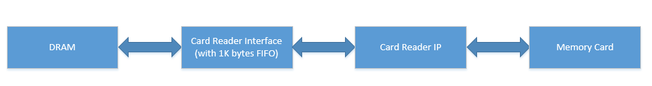
Card Reader Control Flow
Card Insertion and Removal Detection

Descriptor for Read Data

Descriptor for Write Data

Read Data from Memory Card

Write Data to Memory Card

Access to Secure Digital Card & SDIO & Multi-media Card
We support more auto read/write modes in SD/MMC/SDIO module. All the data transfers between XD card and Flash Card Controller are controlled by XD_TRANSFER register. We should set Start bit to start one thorough transfer and polling End bit to check if it completes. The Command Code in XD_TRANSFER register is provided for transfer mode select.
SEND_CMD_GET_RSP command code is for normal operation on SD/MMC/SDIO cards. Hardware start transfer by sending SD command stored in SD_CMD0, SD_CMD1, SD_CMD2, SD_CMD3, SD_CMD4 and get response to Ping-Pong buffer. Use register SD_CONFIGURE2 to specify response length returned.
NORMAL_READ command code is for read short or one page data from SD/MMC/SDIO card such as EXT_CSD. The data destination is specified by CARD_DATA_SOURCE.
NORMAL_WRITE command code is for write 1 or 2 bytes data to SD/MMC/SDIO card. This command code is only for MMC 4.0 Bus Test now.
SD_AUTO_READx, SD_AUTO_WRITEx command code is used in auto read/write data from SD/MMC/SDIO card. Some configuration must be set in advance and SD_BYTE_CNT, SD_BLOCK_CNT shall be specified. Hardware support short block transfer whose block size is less than 512bytes. In this circumstance SD_BYTE_CNT is set to the actual block size. In general condition firmware set SD_BYTE_CNT to 512. SD_BLOCK_CNT decreases after each sector is transferred. If SD_BLOCK_CNT count down to 0, hardware will complete the transfer.
For performance issue, the chip provide four multiple read/write mode:
AUTO_WRITE1:Read Command + Read Response + Get Data + Stop Command + Stop Response
AUTO_WRITE2:Read Command + Read Response + Get Data
AUTO_WRITE3:Get Data
AUTO_WRITE4:Get Data + Stop Command + Stop Response
Refer to SD_TRANSFER for detail.
Read/write error status could be get from SD_STAT and transfer configuration could be set in SD_CFG1 and SD_CFG2.
To support SDIO card we provide SDIO_INT_CTL register to enable/disable SDIO card interrupt signal detect and report interrupt flag in this register too.
The SD/MMC Memory Card system defines two alternative communication protocols: SD/MMC and SPI. The chip uses SD/MMC mode to access. Communication over SD/MMC bus is based on command and data bit streams, which are initialed by a start bit and terminated by a stop bit.
Command: a command is a token, which starts an operation. A command is sent from the host to card. A command is transferred serially on the CMD line.
Response: a response is a token, which is sent from an addressed card to the host as an answer to a previously received command. A response is transferred serially on the CMD line.
Data: data can be transferred from the card to the host or vice versa. Data is transferred via the data lines.
The basic transaction on the SD/MMC bus is the command/response transaction. This type of bus transactions transfer their information directly within the command or response structure. In addition, some operations have a data token.
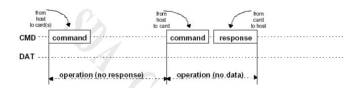
Data transfers to/from the SD Memory Card are done in blocks, data blocks always succeeded by CRC bits. Single and multiple block operations are defined. Note that the Multiple Block operation mode is better for faster write operation. A multiple block transmission is terminated when a stop command follows on the CMD line. Data transfer can be configured by the chip to use single or multiple data lines.

(Multiple) Block read operation
The block write operation uses a simple busy signaling of the write operation duration on the DAT0 data line regardless of the number of data lines used for transferring the data.

(Multiple) Block write operation
Command tokens have the following coding scheme:

Each command token is preceded by a start bit 0 and succeeded by an end bit 1. The total length is 48-bit. Each token is protected by CRC bits so that transmission errors can be detected and the operation may be repeated.
Response tokens have four (SD) or five (MMC) coding schemes depend on their content. The token length is either 48 or 136 bits. The CRC protection algorithm for block data is a 16 bits CCITT polynomial.
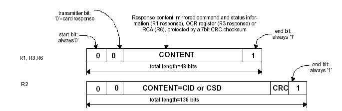
SD Response token format
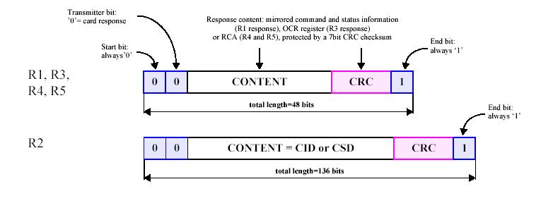
MMC response token format
In the CMD line the MSB bit is transmitted first the LSB bit is the last. When the wide bus option is used, the data is transferred 4/8 bits at a time. Start and end bits, as well as the CRC bits, are transmitted for every one of the DAT lines. CRC bits are calculated and checked for every DAT line individually. The CRC status response and Busy indication will be sent by the card to the chip on DAT0 only (others DAT lines during that period are don’t care).

SD usual data packet format

MMC usual data packet format (1)

MMC usual data packet format (2)
Two operation modes are defined for SD/MMC Memory Card system (Chip and Card):
Card identification mode
The chip will be in card identification mode after reset and while it is looking for new card on the bus. A card will be in this mode after reset until SEND_RCA command (CMD3) is received.
(In case of Multi-Media Card – SET_RCA (CMD3) command). All data communication in the mode uses the command (CMD) only.
Data transfer mode
A card will enter data transfer mode once their RCA is first published. The chip will enter data transfer mode after identifying a card on the bus.
The following table shows the dependencies between bus modes, operation modes and card states.
Card state |
Operation mode |
Bus mode |
|---|---|---|
Stand-by state |
Data transfer mode |
Push-pull |
Transfer state |
Data transfer mode |
Push-pull |
Bus-test state |
Data transfer mode |
Push-pull |
Sending-data state |
Data transfer mode |
Push-pull |
Receive-data state |
Data transfer mode |
Push-pull |
Programming state |
Data transfer mode |
Push-pull |
Disconnect state |
Data transfer mode |
Push-pull |
The following diagram is SD Memory Card state diagram:
SD memory card state (card identification mode)
The following diagram is SD Memory Card Initialization and Identification flow:
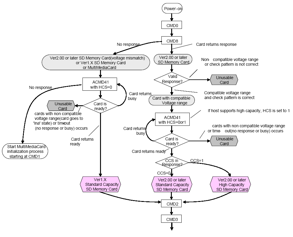
For supporting SD v2.0 high capacity card, SD card identification and initialization flow shall be changed. And the byte address must be changed to sector address in command argument when accessing high capacity SD card.
The following diagram is MMC memory card state identification mode:

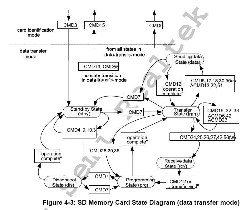
The following diagram is SD Memory Card state diagram in data transfer mode:
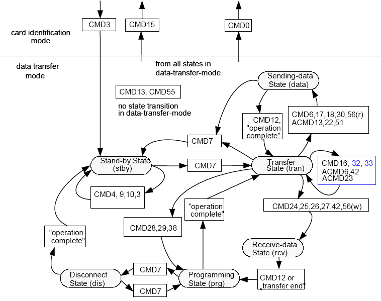
The following diagram is MMC memory card state data transfer mode:

SD Wide Bus (4 bits bus width) operation mode may be selected/deselected using ACMD6 (SET_BUS_WIDTH). The default bus width after power up or GO_IDLE (CMD0) is 1 bit bus width. ACMD6 command is valid in tran. State only, this means that the bus width may be changed only after a SD card was selected (CMD7).
To make SD 2GB card, the Maximum Length (READ_BL_LEN = WRITE_BL_LEN) shall be set to 1024 bytes. But Block Length set by CMD16 shall be up to 512 bytes to keep consistency with 512 bytes Maximum Block Length Cards (less than and equal 2GB cards).
SD Switch function command (CMD6) is used to switch or expand memory card functions. Currently, there are two function groups defined:
Card access mode - 12.5MB/sec interface speed (default) or 25MB/sec interface speed. (High-speed)
Card command system – Standard command set (default) or eCommerce command set or Vendor Specific Command set.
This is a new feature, introduced in SD physical Layer Specification Version 1.10 and later version. Therefore, SD cards that are compatible with earlier versions of the spec do not support it. The chip shall check the SD_SPEC field in the SCR register to recognize what version of the specification the card complies with before using CMD6. It is mandatory for SD memory card of Ver1.10 to support CMD6.
CMD6 is valid under the Transfer State, though once selected, via the switch command, all functions only return to the default function after a power cycle, CMD6 or CMD0. Using CMD0 to reset the card will cause the card to reset to the idle state and all the functions to switch back to the default function.
As a response to CMD6, the SD Memory Card will send R1 response on the CMD line, and 512 bits of status on the DAT lines. From the SD bus transaction point of view, this is a standard single block read transaction and the time out value of this command is 100ms, same as in read command. If CRC error occurs on the status data the chip should issue a power cycle.
CMD6 can be used in two modes:
Mode 0 (check function): used to query if the card supports a specific function or functions.
Mode 1 (set function): used to switch the functionality of the card.

Usage of SD switch command
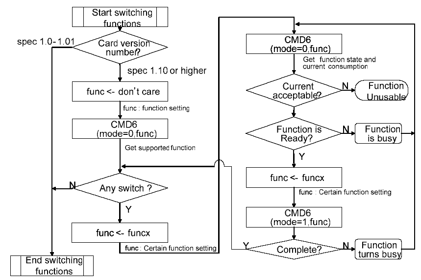
SD switching function flow
Though the Rev 1.01 SD memory card supports up to 12.5MB/sec interface speed, the speed of 25MB/sec is necessary to support increasing performance needs of the host and because of memory size which continues to grow.
To achieve 25MB/sec interface speed, clock rate is increasing to 50MHz and CLK/CMD/DAT signal timing and circuit conditions are reconsidered and changed from older specification version. For high speed card performance issue, the chip provides 50MHz/52MHz clock for SD/MMC card. After power up, the SD memory card is in the default speed mode, and by using Switch Function command (CMD6), the rev 1.10 (and greater) SD memory card can be placed in High-Speed mode.
For SDIO card or I/O portion of a combo card:
Host sends CMD5 prior to the CMD55/ACMD41 pair, and thus would receive a valid OCR in the R4 response to CMD5 and continue to initialize the card. The host read that R4 value and knows the number of available I/O functions and about the existence of any SD memory.
The reset command (CMD0) is only used for memory or memory portion of Combo cards. In order to reset an I/O only card or the I/O portion of a combo card, use CMD52 to write a 1 to the RES bit in the CCCR (bit 3 of register 6). In addition, the SDIO card uses a write to the CCCR using CMD52 to select bus width, connect/disconnect Card Detect Resistor too.
Two additional data transfer instructions have been added to support I/O. IO_RW_DIRECT (CMD52), a direct I/O command similar to the MMC Fast I/O command, and IO_RW_EXTENDED (CMD53), which allows fast access with byte or block address. The IO_RW_DIRECT is the simplest means to access a single register within the total 128K of register space in any I/O function, including the common I/O area (CIA). This command reads or writes 1 byte using only 1 command/response pair. A common use is to initialize register or monitor status for I/O functions. In order to read and write multiple I/O registers with a single command, a new command, IO_RW_EXTENDED (CMD53) is defined. This command allows the reading or writing of a large number of I/O registers with a single command. When executing the IO_RW_RXTENDED (CMD53), the multi-byte or multi-block data transfer is similar to the data transfer for memory. For the multi-byte transfer modes (block mode=0) the following applies:
IO_RW_EXTENDED byte read is similar to CMD17 (READ_SINGLE_BLOCK)
IO_RW_EXTENDED byte write is similar to CMD24 (WRITE_BLOCK)
The byte count for this transfer is set in the command, rather than the fixed block size. Thus, the size of the data payload is in the range of 1-512 bytes. The block mode (block mode=1) is similar to the following memory commands:
IO_RW_EXTENDED block read is similar to CMD18 (READ_MULTIPLE_BLOCK)
IO_RW_EXTENDED block write is similar to CMD17 (WRITE_SINGLE_BLOCK)
For the block mode the only difference is that for a fixed block count, the host does not need to stop the transfer, as it continues until the block count is satisfied. If the block count is set to zero, the operation is identical to the memory mode in that the host must stop the transfer. For an SDIO card, CMD12 is replaced by a write to the ASx bits in the CCCR. The response from SDIO card to CMD52 and CMD53 shall be R5 response.
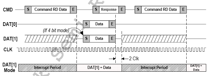
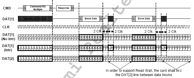
The SDIO card’s interrupt is low-sensitivity, and it use Pin number 8 to interrupt the chip. Since Pin 8 is shared between the IRQ and DAT[1] use in the 4-bit SD mode, an interrupt shall only be sent by the card and recognized by the chip during a special time. The time that a low on Pin 8 shall be recognized as an interrupt is defined as the Interrupt Period. In order to support SDIO Interrupt notification function, the chip hardware shall be capable of detecting interrupt signal on pin DAT[1] regardless of data transfer mode. The chip hardware set 1 to SDIO INT Flag after detecting interrupt signal issued from SDIO card. After interrupt process, the interrupt flag shall be cleared by write 1 to SDIO INT Clear bit. In addition, to be compatible with SD memory card, hardware can enable/disable SDIO interrupt detection function by set/clear SDIO INT Enable0, SDIO INT Enable1. The chip can detect two kinds of SDIO interrupt signals. (Interrupt Period at the Data Block Gap in 4-bit SD mode).
The following diagrams demonstrate SDIO interrupt periods according to various access modes:
SDIO read interrupt cycle timing
SDIO write interrupt cycle timing
SDIO continuous interrupt cycle timing
SDIO multiple block 4-bit read interrupt cycle timing
SDIO multiple block 4-bit write interrupt cycle timing
SDIO specification adds the Read Wait control to enable the host to issue CMD52 during a multiple read cycle. But Read Wait is not supported by the chip now. The following diagrams illustrate the Read Wait procedure and timing:
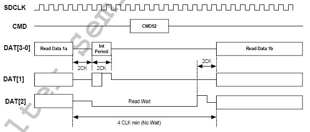
SDIO card read wait delay using DAT[2]
SDIO card DAT[2] drive timing for read wait
The MMC card operates in a given command set, by default, after a power cycle or test by CMD0, it is the Multi-Media Card standard command set, using a single data line, DAT0. The chip can change the active command set by issuing the SWITCH command (CMD6) with the ‘Command Set’ access mode selected.
The supported command sets, as well as the currently selected command set, are defined in the EXT_CSD register. The EXT_CSD register is divided in two segments, a Properties segment and a Modes segment. The properties segment contains information about the card capabilities. The Modes segment reflects the current selected modes of the card.
The chip reads the EXT_CSD register by issuing the SEND_EXT_CSD command. The card sends the EXT_CSD register as a block of data, 512 bytes long. Any reserved, or write only field, read as 0.
The chip can write the Modes segment of the EXT_CSD register by issuing a SWITCH command and setting one of the access modes. All three modes access and modify one of the EXT_CSD bytes, the byte pointed by the Index field.
SWITCH and SEND_EXT_CSD command transfer will be implemented by NORMAL_READ.
Access mode is shown below.
Access bits |
Access name |
Operation |
|---|---|---|
00 |
Command set |
The command set is changed according to the Cmd Set field of the argument. |
01 |
Set bits |
The bits in the pointed byte are set, according to the ‘1’ bits in the Value field. |
10 |
Clear bits |
The bits in the pointed byte are cleared, according to the ‘1’ bits in the Value field. |
11 |
Write byte |
The Value field is written into the pointed byte. |
The SWITCH command can be used either to write the EXT_CSD register or to change the command set. If the SWITCH command is used to change the command set, the Index and Value field are ignored, and the EXT_CSD is not written. If the SWITCH command is used to write the EXT_CSD register, the command set field is ignored, and the command set remains unchanged.
After the chip verifies that the MMC complies with version 4.0 or higher (We can check the SPEC_VERS field of CSD), of his standard, it has to enable the High Speed mode timing in the card, before changing the clock frequency to a frequency higher than 20Mhz. For the chip to change to a higher clock frequency, it has to enable the High Speed interface timing by set Speed Mode to 1. The host uses the SWITCH command to write 0x01 to the HS_TIMING byte, in the Modes segment of the EXT_CSD register.
By issuing MMC commands CMD19 and CMD14 the chip can detect the functional pins on the bus. In a first step, the host sends CMD19 to the card, followed by a specific data pattern on each selected data lines. The data pattern to be sent per data line is defined in the table below. As a second step, the chip sends CMD14 to request the MMC to send back the reversed data pattern. With the data pattern sent by the chip and with the reversed pattern sent back by the card, the functional pins on the bus can be detected.
Start bit |
Data pattern |
End bit |
|---|---|---|
0 |
10xxxx…xx |
1 |
The card ignores all but the two first bits of the data pattern. Therefore, the card buffer size is not limiting the maximum length of the data pattern. The minimum length of the data pattern is two bytes, of which the first two bits of each data line are send back, by the card, reversed. The data pattern sent by the chip may optionally include a CRC16 checksum, which is ignored by the card.
The MMC detects the start bit on the DAT0 and synchronizes accordingly the reading of all its inputs. The chip ignores all but the two first bits of the reverse data pattern and not check CRC16. The length of the reverse data pattern is eight bytes and is always sent using all the card’s DAT lines, refers to the following tables. The reverse data pattern sent by the card may optionally include a CRC16 checksum, which is ignored by the chip.
MMC 1-bit bus testing pattern is shown below.
Data line |
Data pattern sent by the host |
Reserved pattern sent by the host |
Notes |
|---|---|---|---|
DAT0 |
0, 10xxxxxxxxxx, [CRC16], 1 |
0, 01000000, [CRC16], 1 |
Start bit defines beginning of pattern |
DAT1 |
0, 00000000, [CRC16], 1 |
No data pattern sent |
|
DAT2 |
0, 00000000, [CRC16], 1 |
No data pattern sent |
|
DAT3 |
0, 00000000, [CRC16], 1 |
No data pattern sent |
|
DAT4 |
0, 00000000, [CRC16], 1 |
No data pattern sent |
|
DAT5 |
0, 00000000, [CRC16], 1 |
No data pattern sent |
|
DAT6 |
0, 00000000, [CRC16], 1 |
No data pattern sent |
|
DAT7 |
0, 00000000, [CRC16], 1 |
No data pattern sent |
MMC 4-bit bus testing pattern is shown below.
Data line |
Data pattern sent by the host |
Reserved pattern sent by the host |
Notes |
|---|---|---|---|
DAT0 |
0, 10xxxxxxxxxx, [CRC16], 1 |
0, 01000000, [CRC16], 1 |
Start bit defines beginning of pattern |
DAT1 |
0, 01xxxxxxxxxx, [CRC16], 1 |
0, 10000000, [CRC16], 1 |
|
DAT2 |
0, 10xxxxxxxxxx, [CRC16], 1 |
0, 01000000, [CRC16], 1 |
|
DAT3 |
0, 01xxxxxxxxxx, [CRC16], 1 |
0, 10000000, [CRC16], 1 |
|
DAT4 |
0, 00000000, [CRC16], 1 |
No data pattern sent |
|
DAT5 |
0, 00000000, [CRC16], 1 |
No data pattern sent |
|
DAT6 |
0, 00000000, [CRC16], 1 |
No data pattern sent |
|
DAT7 |
0, 00000000, [CRC16], 1 |
No data pattern sent |
MMC 8-bit bus testing pattern is shown below.
Data line |
Data pattern sent by the host |
Reserved pattern sent by the host |
Notes |
|---|---|---|---|
DAT0 |
0, 10xxxxxxxxxx, [CRC16], 1 |
0, 01000000, [CRC16], 1 |
Start bit defines beginning of pattern |
DAT1 |
0, 01xxxxxxxxxx, [CRC16], 1 |
0, 10000000, [CRC16], 1 |
|
DAT2 |
0, 10xxxxxxxxxx, [CRC16], 1 |
0, 01000000, [CRC16], 1 |
|
DAT3 |
0, 01xxxxxxxxxx, [CRC16], 1 |
0, 10000000, [CRC16], 1 |
|
DAT4 |
0, 10xxxxxxxxxx, [CRC16], 1 |
0, 01000000, [CRC16], 1 |
|
DAT5 |
0, 01xxxxxxxxxx, [CRC16], 1 |
0, 10000000, [CRC16], 1 |
|
DAT6 |
0, 10xxxxxxxxxx, [CRC16], 1 |
0, 01000000, [CRC16], 1 |
|
DAT7 |
0, 01xxxxxxxxxx, [CRC16], 1 |
0, 10000000, [CRC16], 1 |
After the host has verified the functional pins on the bus it should change the bus width configuration accordingly, using the SWITCH command. The bus width configuration is changed by writing to the BUS_WIDTH byte in the Modes Segment of the EXT_CSD register (using the SWITCH command to do so). After power-on or software reset, the contents of the BUS_WIDTH byte is 0x00.
Card Interface Signals
Secure Digital Card/Multi-media Card Interface
Name |
Type |
I/O Type |
Pin No. |
Description |
|---|---|---|---|---|
SD_CD# |
I |
IPU |
SD/SDIO/MMC Card detect pin |
|
SD_CMD |
I/O |
IPU80/O8 |
Serial protocol command and response signal |
|
SD_DAT [7:0] |
I/O |
IPU80/O8 |
SD/SDIO/MMC data signals |
|
SD_CLK |
O |
O8 |
Serial protocol clock signal |
|
SD_WP |
I |
IPU |
SD Write Protect switch signal |
Power and Ground
Name |
Type |
I/O Type |
Pin No. |
Description |
|---|---|---|---|---|
G18 |
Power |
Ground |
Analog ground (1V8) |
|
V18 |
Power |
Power |
Analog regulated supply voltage (1.8V??F0B1??10%) from internal 3.3V to 1.8V regulator; supplies internal digital circuits. An external capacitance should be connected. |
|
D3V3 |
Power |
Power |
Digital power |
|
DGND |
Power |
Ground |
Digital ground |
|
3V3_IN |
Power |
Power |
3.3V input to internal regulator (3.3V to 1.8V) |
|
AUX_3V3 |
Power |
Power |
Auxiliary power |
|
CARD_3V3 |
Power |
Power |
Card 3V3 power |
Registers
SDIO Wrapper Control Registers
Base address: 0x1801_0A00
Register table: https://rtitrsvn.rtkbf.com/svn/Ameba/branches/AmebaSmart/eflow/espec/dip/sdio_host/es013_RL6678_sdio_wrapper_reg_spec.xls
SD Wrapper Control Registers
Base address: 0x5000_0000
Register table: https://rtitrsvn.rtkbf.com/svn/Ameba/branches/AmebaSmart/eflow/espec/dip/sdio_host/es013_RL6678_sd_wrapper_reg_spec.xls
SD IP Registers
Base address: 0x1801_0500
Register table: https://rtitrsvn.rtkbf.com/svn/Ameba/branches/AmebaSmart/eflow/espec/dip/sdio_host/es013_RL6678_SD_IP_reg_spec.xls
eMMC Wrapper Control Registers
Base address: 0x1801_2000
Register table: https://rtitrsvn.rtkbf.com/svn/Ameba/branches/AmebaSmart/eflow/espec/dip/sdio_host/es013_RL6678_eMMC_wrapper_reg_spec.xls
eMMC IP Registers
Base address: 0x1801_2100
Register table: https://rtitrsvn.rtkbf.com/svn/Ameba/branches/AmebaSmart/eflow/espec/dip/sdio_host/es013_RL6678_EMMC_IP_reg_spec.xls
Application Specification
Data Path
Address
Secure Digital (SD)
Data address is in byte units in a Standard Capacity SD Memory Card.
Data address is in block (512 bytes) units in a High Capacity SD Memory Card.
Multi-Media Card (MMC)
Data address is in byte units in a Multi-Media Card.
Data address is in sector (512 bytes) units in a Multi-Media Card (> 2GB).
Memory Stick (MS)
Data address is in page (512 bytes) units in a MS Card.
Memory Stick Pro (MS Pro)
Data address is in sector (512 bytes) units in a MS Pro Card.
I/O Flow
Secure Digital (SD)
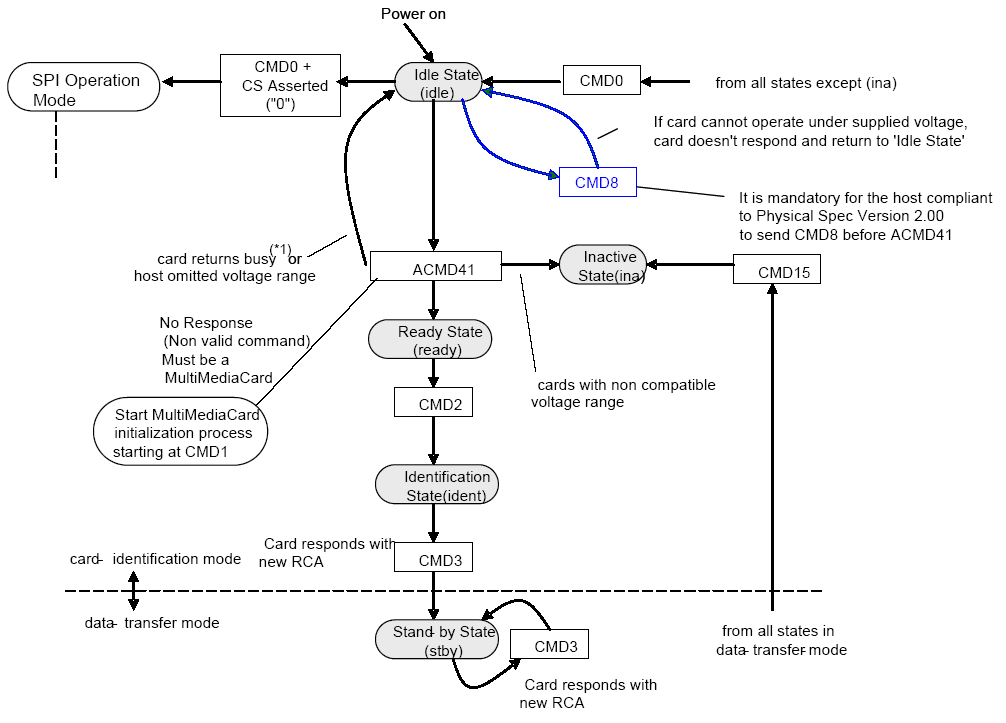
Card Initialization and Identification Flow
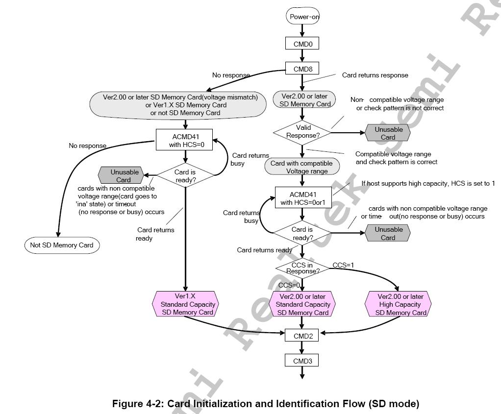
CMD0: GO_IDLE_STATE: Resets all cards to idle state
CMD8: SEND_IF_COND: Sends SD Memory Card interface condition, which includes host supply voltage information and asks the card whether card supports voltage
CMD55: Indicates to the card that the next command is an application specific command rather than a standard command
ACMD41: SD_SEND_OP_COND: Sends host capacity support information (HCS) and asks the accessed card to send its operating condition register (OCR) content in the response on the CMD line
CMD2: ALL_SEND_CID: Asks any card to send the CID numbers on the CMD line (any card that is connected to the host will respond)
CMD3: SEND_RELATIVE_ADDR: Ask the card to publish a new relative address (RCA)
Data Transfer Mode
CMD15: GO_INACTIVE_STATE: Sends an addressed card into the Inactive State.
CMD7: SELECT/DESELECT_CARD: Command toggles a card between the stand-by and transfer states or between the programming and dis-connected states.
ACMD6: Defines the data bus width (
'00'=1bit or '10'=4 bits bus) to be used for data transfer.CMD12: STOP_TRANSMISSION: Forces the card to stop transmission
CMD17: READ_SINGLE_BLOCK
CMD18: READ_MULTIPLE_BLOCK
CMD24: WRITE_SINGLE_BLOCK
CMD25: WRITE_MULTIPLE_BLOCK
Multi-Media Card (MMC)
Card Identification Mode
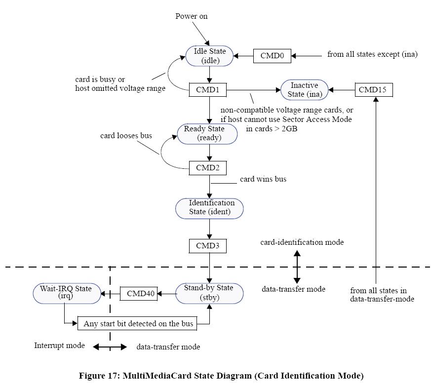
CMD1: SEND_OP_COND: Asks the card, in idle state, to send its Operating Conditions Register contents in the response on the CMD line.
CMD40: GO_IRQ_STATE: Sets the system into interrupt mode
Data Transfer Mode
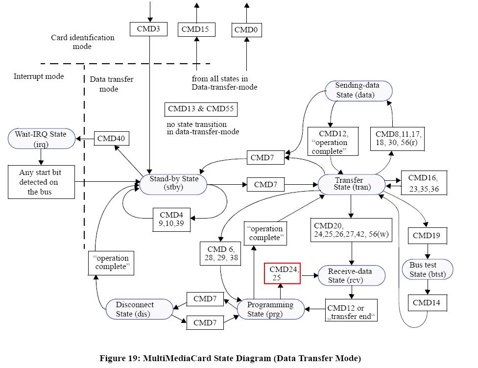
First of all the address argument for higher than 2GB of density of memory is changed to be sector address (512B sectors) instead of byte address.
Secondly the density of the card is read from the EXT_CSD register instead of CSD register
CMD6: Switches the mode of operation of the selected card or modifies the EXT_CSD registers.
BUS_WIDTH:
0b: 1-bit
1b: 4-bit
2b: 8-bit
CMD8: The card sends its EXT_CSD register as a block of data.
CMD12: STOP_TRANSMISSION: Forces the card to stop transmission
CMD17: READ_SINGLE_BLOCK
CMD18: READ_MULTIPLE_BLOCK
CMD24: WRITE_SINGLE_BLOCK
CMD25: WRITE_MULTIPLE_BLOCK
Memory Stick Pro (MS Pro)
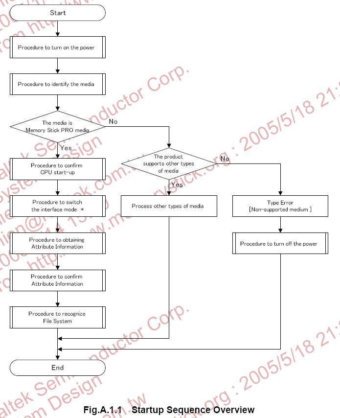
Startup Sequence Overview
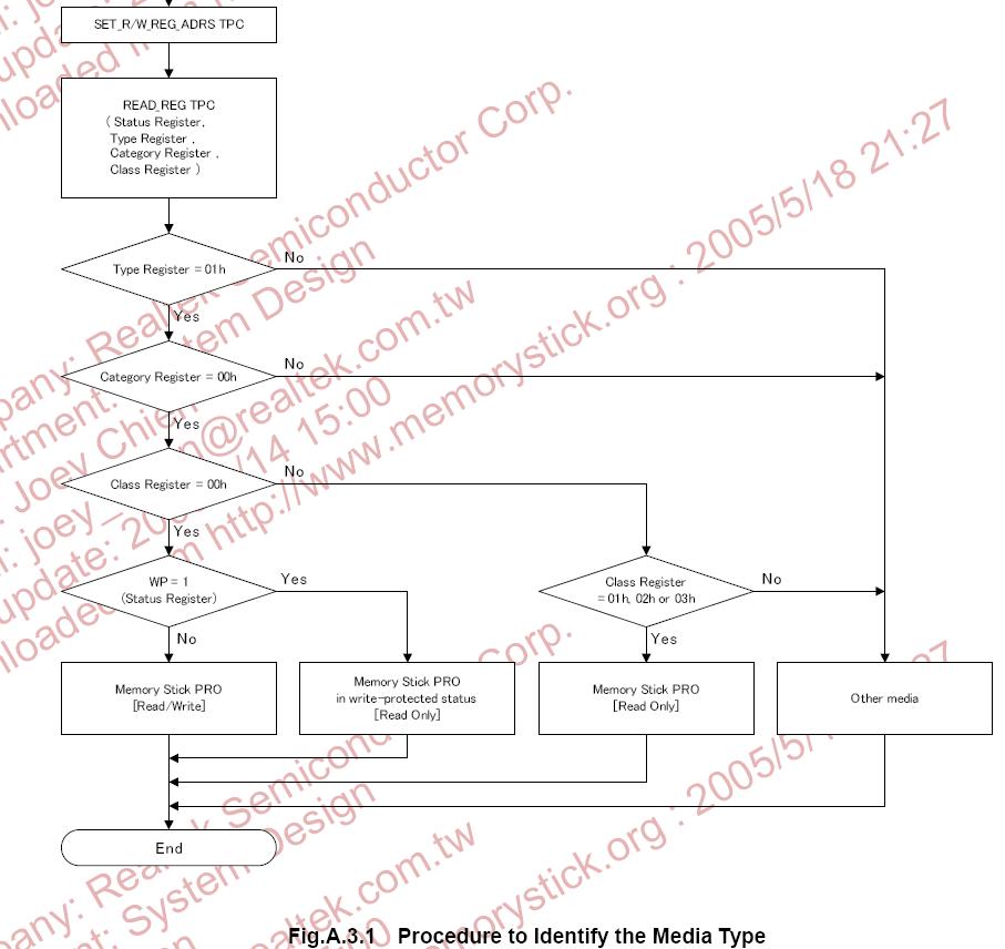
Identification Flow
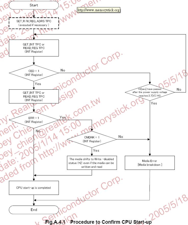
CPU Startup Sequence
Type Register
0x00: Memory Stick0x01: Memory Stick Pro
INT Register
IO[7]: CED: Command EndIO[6]: ERR: ErrorIO[5]: BREQ: Buffer RequestIO[0]: CMDNK: Command cannot be executed
Switch Interface Mode
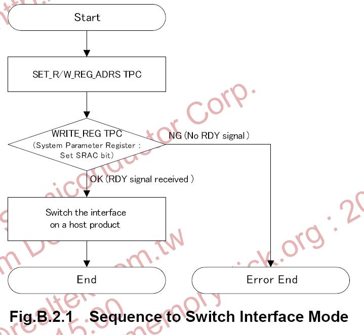
System Parameter Register
IO[7]: SRAC (Serial Access):0: Parallel Interface1: Serial Interface
After Switch Interface Mode complete, we need to send MS_SetParameter command to switch card reader controller’s interface.
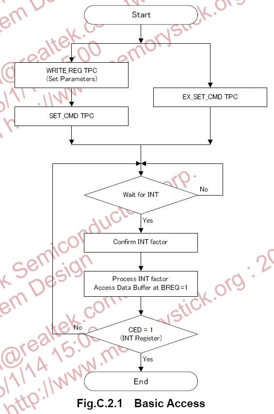
Basic Access Flow
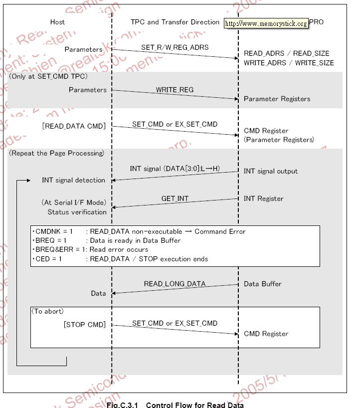
Control Flow for Read Data
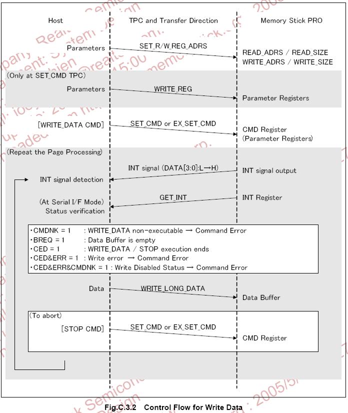
Control Flow for Write Data
Application
Firmware Upgrade with Card Reader
User select an image file via UI
AP reads the image file to specific memory address
Firmware upgrader writes image to SPI flash or NAND flash.
Usage
File System Side
Using SCSI Command Set
Disk Capacity Information
I/O Read
I/O Write
Application Side
File I/O API
Logo
SD/MMC Compatibility Test
MS/MS Pro Compatibility Test
Electrical characteristics
SDIO host IP supports 3.3V/1.8V two IO power working modes. But when SDIO host works in 1.8V IO power mode, because IC cannot switch IO power through software, it does not support cards that need to switch between 3.3V and 1.8V IO power between initialization and communication.