Elliptic Curve Signature Algorithm (ECDSA)
Overall Description
Elliptic Curves over Finite Fields
Let p > 3 be an odd prime. An elliptic curve E over Fp is defined by an equation of the form
where a, b ∈ Fp, and 4a³ + 27b² ≢ 0 (mod p). The set E (Fp) consists of all point (x, y), x ∈ Fp, y ∈ Fp, which satisfy the defining equation, together with a special point O called the point at infinity.
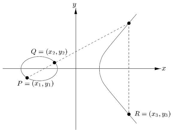
The following algebraic formula for the sum of two points and the double of a point can now be derived from the geometric description.
P + O = O + P = P for all P ∈ E(Fp)
If P = (x,y) ∈ E(Fp), then (x,y) + (x,-y) = O
(Point addition) Let P = (x1,y1) ∈ E(Fp) and Q = (x2,y2) ∈ E(Fp), where P ≠ ±Q. Then P + Q = (x3,y3), where
\[x3 = \left(\frac{y2-y1}{x2-x1}\right)^2 - x1 - x2 \quad \text{and} \quad y3 = \left(\frac{y2-y1}{x2-x1}\right)^2(x1 - x3) - y1\](Point doubling) Let P = (x1,y1) ∈ E(Fp), where P ≠ -P. Then 2P = (x3,y3), where
\[x3 = \left(\frac{3x1^2+a}{2y1}\right)^2 - x1 - x1 \quad \text{and} \quad y3 = \left(\frac{3x1^2+a}{2y1}\right)^2(x1 - x3) - y1\]
ECDSA Key Pair Generation
An entity A’s key pair is associated with a particular set of EC parameters D = (n, a, b, G, p, hash). This association can be assured cryptographically (e.g., with certificates) or by context (e.g., all entities use the same domain parameters). The entity A must have the assurance that the domain parameters are valid prior to key generation.
For ECDSA key pair generation, each entity A does the following:
Select a random or pseudorandom integer “Pri” in the interval [1, n − 1].
Compute Pub = Pri * G.
A’s public key is “Pub”; A’s private key is “Pri”.
ECDSA Signature Generation and Verification
Signature
To sign a message m, an entity A with domain parameters D = (n, a, b, G, p, hash) and associated key pair (Pri, Pub) does the following:
Select a random or pseudorandom integer k, 1 ≤ k ≤ n − 1.
Compute k * G = (x1,y1) and convert x1 to an integer x̄1.
Compute R = x1 mod n. If r = 0 then go to step 1.
Compute k⁻¹ mod n.
Compute SHA − 1(m) and convert this bit string to an integer “hash”.
Compute S = k⁻¹(hash + Pri * R) mod n. If S = 0 then go to step 1.
A’s signature for the message m is (R,S).
Verification
To verify A’s signature (R,S) on m, B obtains an authentic copy of A’s domain parameters D = (n,a,b,G,p,hash) and associated public key Q. B then does the following:
Verify the R and S are integers in the interval [1, n − 1].
Compute SHA − 1(m) and convert this bit string to an integer “hash”.
Compute S⁻¹ mod n.
Compute U₁ = hash * S⁻¹ mod n and U₂ = R * S⁻¹ mod n.
Compute X = U₁ * G + U₂ * Pub.
If X = O, then reject the signature. Otherwise, convert the x-coordinate x₁ of X to an integer x̄1, and compute v = x̄1 mod n.
Accept the signature if and only if v = R.
Proof that Signature Verification Works
If a signature (R,S) on a message m was indeed generated by A, then
S = k⁻¹(hash + Pri * R) mod n. Rearranging gives
Thus
and so v = R as required.
Features
Supported operations:
Verification (reg_mode_sel == 2’d0)
Signature (reg_mode_sel == 2’d1)
Scalar multiplication (reg_mode_sel == 2’d2, {eng_xo, eng_yo} = eng_h * {eng_x, eng_y})
Basic function (reg_mode_sel == 2’d3)
reg_func_sel[2:0] |
Function description |
|---|---|
1XX |
add_point: {eng_xo, eng_yo} = {eng_x, eng_y} + {eng_gx, eng_gy} |
000 |
sub_mod: {eng_xo, eng_yo} = (eng_x - eng_y) % prime |
001 |
div_mod: {eng_xo, eng_yo} = (eng_x/eng_y) % prime |
010 |
add_mod: {eng_xo, eng_yo} = (eng_x + eng_y) % prime |
011 |
mul_mod: {eng_xo, eng_yo} = (eng_x * eng_y) % prime |
Block Diagram

Functional Description
The ECDSA implements a complete asymmetric (public/private) key cryptographic signature solution based upon Elliptic Curve Cryptography and the ECDSA signature protocol. The device features hardware acceleration for the NIST standard Secp256k1 and P256 prime curve includes ECDSA signature generation, ECDH key agreement, and ECDSA public key signature verification.
Startup Step
Enable the clock, and set reg_eng_clk enable = 1. (0x000)
Reset the ECDSA, reg_eng_rst = 1. (0x000)
Reset the ECDSA, reg_eng_rst = 0. (0x000)
Set the input data.
Set eng_start = 1. (0x008)
ECDSA Interrupt
The assertion of the ECDSA interrupt occurs when the calculation is completed. When the interrupt is occurred the software can access the EISR (0x008) to identify the interrupt type.
Registers
Introduction
The ECDSA has a number of internal registers that are accessed through the 12-bit address bus.
reg_mode_sel=0, verification
Input |
Pin Name |
Offset |
|---|---|---|
public key x |
eng_x |
0x010~0x02C |
public key y |
eng_y |
0x030~0x04C |
hash |
eng_h |
0x150~0x16C |
R |
eng_verify_r |
0x110~0x12C |
S |
eng_verify_s |
0x130~0x14C |
base point x (gx) |
eng_gx |
0x050~0x06C |
base point y (gy) |
eng_gy |
0x070~0x08C |
cor_a |
cor_a |
0x170~0x18C |
prime |
prime |
0x190~0x1AC |
order_n |
order_n |
0x1B0~0x1CC |
Output |
Pin Name |
Offset |
|---|---|---|
R_x |
eng_xo |
0x090~0x0AC |
R_y |
eng_yo |
0x0B0~0x0CC |
verify_pass |
verify_pass |
0x008 |
verify_err |
verify_err |
0x008 |
infinity_err |
infinity_err |
0x008 |
eng_finish |
eng_finish |
0x008 |
reg_mode_sel=1, signature
Input |
Pin Name |
Offset |
|---|---|---|
private key |
eng_x |
0x010~0x02C |
random k |
eng_y |
0x030~0x04C |
hash |
eng_h |
0x150~0x16C |
base point x(gx) |
eng_gx |
0x050~0x06C |
base point y(gy) |
eng_gy |
0x070~0x08C |
cor_a |
cor_a |
0x170~0x18C |
prime |
prime |
0x190~0x1AC |
order_n |
order_n |
0x1B0~0x1CC |
Output |
Pin Name |
Offset |
|---|---|---|
public key x |
eng_xo |
0x090~0x0AC |
public key y |
eng_yo |
0x0B0~0x0CC |
R |
eng_sign_r |
0x0D0~0x0EC |
S |
eng_sign_s |
0x0F0~0x10C |
sign_err |
sign_err |
0x008 |
infinity_err |
infinity_err |
0x008 |
eng_finish |
eng_finish |
0x008 |
reg_mode_sel=2, scalar multiplication
Input |
Pin Name |
Offset |
|---|---|---|
private key |
eng_h |
0x150~0x16C |
base point x (gx) |
eng_x |
0x010~0x02C |
base point y (gy) |
eng_y |
0x030~0x04C |
cor_a |
cor_a |
0x170~0x18C |
prime |
prime |
0x190~0x1AC |
order_n |
order_n |
0x1B0~0x1CC |
Output |
Pin Name |
Offset |
|---|---|---|
public key x |
eng_xo |
0x090~0x0AC |
public key y |
eng_yo |
0x0B0~0x0CC |
share_key_err |
share_key_err |
0x008 |
infinity_err |
infinity_err |
0x008 |
eng_finish |
eng_finish |
0x008 |
reg_mode_sel=3, basic function
Input |
Pin Name |
Offset |
|---|---|---|
eng_x |
eng_x |
0x010~0x02C |
eng_y |
eng_y |
0x030~0x04C |
eng_gx |
eng_gx |
0x050~0x06C |
eng_gy |
eng_gy |
0x070~0x08C |
cor_a |
cor_a |
0x170~0x18C |
prime |
prime |
0x190~0x1AC |
Output |
Pin Name |
Offset |
|---|---|---|
public key x |
eng_xo |
0x090~0x0AC |
public key y |
eng_yo |
0x0B0~0x0CC |
infinity_err |
infinity_err |
0x008 |
eng_finish |
eng_finish |
0x008 |
Field Description
NA.
Base Address: 0x4011F000
Name |
Address offset |
Access |
Description |
|---|---|---|---|
000h |
R/W |
||
004h |
R/W |
||
008h |
R/W |
||
00Ch |
R/W |
||
010h |
R/W |
||
014h |
R/W |
||
018h |
R/W |
||
01Ch |
R/W |
||
020h |
R/W |
||
024h |
R/W |
||
028h |
R/W |
||
02Ch |
R/W |
||
030h |
R/W |
||
034h |
R/W |
||
038h |
R/W |
||
03Ch |
R/W |
||
040h |
R/W |
||
044h |
R/W |
||
048h |
R/W |
||
04Ch |
R/W |
||
050h |
R/W |
||
054h |
R/W |
||
058h |
R/W |
||
05Ch |
R/W |
||
060h |
R/W |
||
064h |
R/W |
||
068h |
R/W |
||
06Ch |
R/W |
||
070h |
R/W |
||
074h |
R/W |
||
078h |
R/W |
||
07Ch |
R/W |
||
080h |
R/W |
||
084h |
R/W |
||
088h |
R/W |
||
08Ch |
R/W |
||
090h |
R |
||
094h |
R |
||
098h |
R |
||
09Ch |
R |
||
0A0h |
R |
||
0A4h |
R |
||
0A8h |
R |
||
0ACh |
R |
||
0B0h |
R |
||
0B4h |
R |
||
0B8h |
R |
||
0BCh |
R |
||
0C0h |
R |
||
0C4h |
R |
||
0C8h |
R |
||
0CCh |
R |
||
0D0h |
R |
||
0D4h |
R |
||
0D8h |
R |
||
0DCh |
R |
||
0E0h |
R |
||
0E4h |
R |
||
0E8h |
R |
||
0ECh |
R |
||
0F0h |
R |
||
0F4h |
R |
||
0F8h |
R |
||
0FCh |
R |
||
100h |
R |
||
104h |
R |
||
108h |
R |
||
10Ch |
R |
||
110h |
R/W |
||
114h |
R/W |
||
118h |
R/W |
||
11Ch |
R/W |
||
120h |
R/W |
||
124h |
R/W |
||
128h |
R/W |
||
12Ch |
R/W |
||
130h |
R/W |
||
134h |
R/W |
||
138h |
R/W |
||
13Ch |
R/W |
||
140h |
R/W |
||
144h |
R/W |
||
148h |
R/W |
||
14Ch |
R/W |
||
150h |
R/W |
||
154h |
R/W |
||
158h |
R/W |
||
15Ch |
R/W |
||
160h |
R/W |
||
164h |
R/W |
||
168h |
R/W |
||
16Ch |
R/W |
||
170h |
R/W |
||
174h |
R/W |
||
178h |
R/W |
||
17Ch |
R/W |
||
180h |
R/W |
||
184h |
R/W |
||
188h |
R/W |
||
18Ch |
R/W |
||
190h |
R/W |
INI value: ffff_fc2f |
|
194h |
R/W |
INI value: ffff_fffe |
|
198h |
R/W |
INI value: ffff_ffff |
|
19Ch |
R/W |
INI value: ffff_ffff |
|
1A0h |
R/W |
INI value: ffff_ffff |
|
1A4h |
R/W |
INI value: ffff_ffff |
|
1A8h |
R/W |
INI value: ffff_ffff |
|
1ACh |
R/W |
INI value: ffff_ffff |
|
1B0h |
R/W |
INI value: d036_4141 |
|
1B4h |
R/W |
INI value: bfd2_5e8c |
|
1B8h |
R/W |
INI value: af48_a03b |
|
1BCh |
R/W |
INI value: baae_dce6 |
|
1C0h |
R/W |
INI value: ffff_fffe |
|
1C4h |
R/W |
INI value: ffff_ffff |
|
1C8h |
R/W |
INI value: ffff_ffff |
|
1CCh |
R/W |
INI value: ffff_ffff |
|
200h |
R |
REG_ECR1
Name : ECDSA Control Register 1
Size : 32
Address offset : 000h
Read/write access : R/W
Bit |
Symbol |
Access |
Reset |
Description |
|---|---|---|---|---|
31:9 |
RSVD |
R |
- |
Reserved |
8 |
REG_ENG_CLK_ENABLE |
R/W |
1’b1 |
ECDSA engine clock enable signal. |
7:1 |
RSVD |
R |
- |
Reserved |
0 |
REG_ENG_RST |
R/W |
1’b0 |
ECDSA reset. Used to reset flip-flop that are clocked by th e eng_clk. |
REG_ESCR
Name : ECDSA Swap Control Register
Size : 32
Address offset : 004h
Read/write access : R/W
Bit |
Symbol |
Access |
Reset |
Description |
|---|---|---|---|---|
31:14 |
RSVD |
R |
- |
Reserved |
13 |
REG_SIGN_S_SWAP |
R/W |
1’b0 |
Byte swap for eng_sign_s |
12 |
REG_SIGN_R_SWAP |
R/W |
1’b0 |
Byte swap for eng_sign_r |
11 |
REG_ORDER_N_SWAP |
R/W |
1’b0 |
Byte swap for order_n |
10 |
REG_H_SWAP |
R/W |
1’b0 |
Byte swap for eng_h |
9 |
REG_PRIME_SWAP |
R/W |
1’b0 |
Byte swap for prime |
8 |
REG_COR_A_SWAP |
R/W |
1’b0 |
Byte swap for cor_a |
7 |
REG_YO_SWAP |
R/W |
1’b0 |
Byte swap for eng_yo |
6 |
REG_XO_SWAP |
R/W |
1’b0 |
Byte swap for eng_xo |
5 |
REG_VERIFY_S_SWAP |
R/W |
1’b0 |
Byte swap for eng_verify_s |
4 |
REG_VERIFY_R_SWAP |
R/W |
1’b0 |
Byte swap for eng_verify_r |
3 |
REG_GY_SWAP |
R/W |
1’b0 |
Byte swap for eng_gy |
2 |
REG_GX_SWAP |
R/W |
1’b0 |
Byte swap for eng_gx |
1 |
REG_Y_SWAP |
R/W |
1’b0 |
Byte swap for eng_y |
0 |
REG_X_SWAP |
R/W |
1’b0 |
Byte swap for eng_x |
REG_EISR
Name : ECDSA Interrupt Status Register
Size : 32
Address offset : 008h
Read/write access : R/W
Bit |
Symbol |
Access |
Reset |
Description |
|---|---|---|---|---|
31:18 |
RSVD |
R |
- |
Reserved |
17 |
INFINITY_ERR |
R |
1’b0 |
This bit indicates that the output coordinates are at infini ty. |
16 |
SHARE_KEY_ERR |
R |
1’b0 |
When secret_key < 1, or secret_key > (order_n-1), the bit i s set to 1. |
15:12 |
SIGN_ERR |
R |
4’b0 |
Error message description
|
11:10 |
VERIFY_ERR |
R |
2’b0 |
Error message description
|
9 |
VERIFY_PASS |
R |
1’b0 |
Verification is completed successfully. |
8 |
ECDSA_FINISH_INT |
R/W |
1’b0 |
ECDSA interrupt status. This bit is cleaned by writing 1. If ecdsa_finish_int_mask is configured to 0, it only masks ecds a_int trigger, ecdsa_finish_int still holds the status. |
7:5 |
RSVD |
R |
- |
Reserved |
4 |
ENG_IDLE |
R |
1’b1 |
When the ECDSA is idle, the bit is set to 1. |
3 |
RSVD |
R |
- |
Reserved |
2 |
HASH_OK |
R/W |
1’b0 |
After the calculation of SHA (m) is completed, this bit will be set to 1 by the software. |
1:0 |
ENG_START |
R/W |
2’b0 |
When this bit is set to 1, ECDSA will start the operation ac cording to the corresponding register. |
REG_ECR2
Name : ECDSA Control Register 2
Size : 32
Address offset : 00Ch
Read/write access : R/W
Bit |
Symbol |
Access |
Reset |
Description |
|---|---|---|---|---|
31:15 |
RSVD |
R |
- |
Reserved |
14 |
EXTEND_N |
R/W |
1’b0 |
When this bit is set to 1, order_n will extend out of 8 bits .
Others: 256-bit |
13:12 |
PRI_KEY_SEL |
R/W |
2’b0 |
Reserved bits. |
11 |
HASH256_EN |
R/W |
1’b0 |
If the length of the hash message exceeds 128-bit, use this function to speed up the operation. |
10:8 |
BIT_NUM |
R/W |
3’b0 |
Select bit_num for correspoinding bit length, when “exten_n” is set to 0.
Others: 256-bit |
7 |
ECDSA_FINISH_INT_MASK |
R/W |
1’b0 |
Mask ECDSA engine interrupt. When the ecdsa_finish_int = 1’b1, if ecdsa_finish_int_mask = 1’b1, then the bit masks ecdsa_int. It means that ecdsa_int = 1’b0, but the ecdsa_finish_int status still holds the valu e(1’b1) in EISR register. |
6:4 |
REG_FUNC_SEL |
R/W |
3’b0 |
The bit is used to select the operation in basic function mo de. The bits are valid when reg_mode_sel[1:0] is set to 2’b1 1.
|
3:2 |
REG_MODE_SEL |
R/W |
2’b0 |
Select operating mode
|
1:0 |
CURVE_SEL |
R/W |
2’b0 |
Select the ECC curve
|
REG_ENG_X_Px
Name : ENG_X_P Register x
Size : 32
Address offset : 010h + 04h * x (x=0, 1, 2, 3, 4, 5, 6, 7)
Read/write access : R/W
Bit |
Symbol |
Access |
Reset |
Description |
|---|---|---|---|---|
31:0 |
ENG_X_Px |
R/W |
0 |
Date register Verification mode: Public key x Signature mode: Private key Scalar multiplication mode: Base point x Basic function mode: Operand |
REG_ENG_Y_Px
Name : ENG_Y_P Register x
Size : 32
Address offset : 030h + 04h * x (x=0, 1, 2, 3, 4, 5, 6, 7)
Read/write access : R/W
Bit |
Symbol |
Access |
Reset |
Description |
|---|---|---|---|---|
31:0 |
ENG_Y_Px |
R/W |
0 |
Date register Verification mode: Public key y Signature mode: Random k Scalar multiplication mode: Base point y Basic function mode: Operand |
REG_ENG_GX_PSx
Name : ENG_GX_PS Register x
Size : 32
Address offset : 050h + 04h * x (x=0, 1, 2, 3, 4, 5, 6, 7)
Read/write access : R/W
Bit |
Symbol |
Access |
Reset |
Description |
|---|---|---|---|---|
31:0 |
ENG_GX_PSx |
R/W |
16f8_1798 |
Because the default cur_sel[1:0] = 2’d0 (secp256k1), so thes e register initial values are secp256k1 setting values. Verification mode: Base point x Signature mode: Base point x Scalar multiplication mode: Base point x Basic function mode: |
REG_ENG_GY_PSx
Name : ENG_GY_PS Register x
Size : 32
Address offset : 070h + 04h * x (x=0, 1, 2, 3, 4, 5, 6, 7)
Read/write access : R/W
Bit |
Symbol |
Access |
Reset |
Description |
|---|---|---|---|---|
31:0 |
ENG_GY_PSx |
R/W |
fb10_d4b8 |
Because the default cur_sel[1:0] = 2’d0 (secp256k1), so thes e register initial values are secp256k1 setting values. Verification mode: Base point y Signature mode: Base point y Scalar multiplication mode: Base point y Basic function mode: |
REG_ENG_XO_Px
Name : ENG_XO_P Register x
Size : 32
Address offset : 090h + 04h * x (x=0, 1, 2, 3, 4, 5, 6, 7)
Read/write access : R
Bit |
Symbol |
Access |
Reset |
Description |
|---|---|---|---|---|
31:0 |
ENG_XO_Px |
R |
0 |
Date register Verification mode: R_x Signature mode: Public x Scalar multiplication mode: Public x Basic function mode: Coordinate x |
REG_ENG_YO_Px
Name : ENG_YO_P Register x
Size : 32
Address offset : 0B0h + 04h * x (x=0, 1, 2, 3, 4, 5, 6, 7)
Read/write access : R
Bit |
Symbol |
Access |
Reset |
Description |
|---|---|---|---|---|
31:0 |
ENG_YO_Px |
R |
0 |
Date register Verification mode: R_y Signature mode: Public y Scalar multiplication mode: Public y Basic function mode: Coordinate y |
REG_ENG_SIGN_R_Sx
Name : ENG_SIGN_R_S Register x
Size : 32
Address offset : 0D0h + 04h * x (x=0, 1, 2, 3, 4, 5, 6, 7)
Read/write access : R
Bit |
Symbol |
Access |
Reset |
Description |
|---|---|---|---|---|
31:0 |
ENG_SIGN_R_Sx |
R |
0 |
Date register Verification mode: Signature mode: R Scalar multiplication mode: Basic function mode: |
REG_ENG_SIGN_S_Sx
Name : ENG_SIGN_S_S Register x
Size : 32
Address offset : 0F0h + 04h * x (x=0, 1, 2, 3, 4, 5, 6, 7)
Read/write access : R
Bit |
Symbol |
Access |
Reset |
Description |
|---|---|---|---|---|
31:0 |
ENG_SIGN_S_Sx |
R |
0 |
Date register Verification mode: Signature mode: S Scalar multiplication mode: Basic function mode: |
REG_ENG_VERIFY_R_Px
Name : ENG_VERIFY_R_P Register x
Size : 32
Address offset : 110h + 04h * x (x=0, 1, 2, 3, 4, 5, 6, 7)
Read/write access : R/W
Bit |
Symbol |
Access |
Reset |
Description |
|---|---|---|---|---|
31:0 |
ENG_VERIFY_R_Px |
R/W |
0 |
Date register Verification mode: R Signature mode: Scalar multiplication mode: Basic function mode: |
REG_ENG_VERIFY_S_Px
Name : ENG_VERIFY_S_P Register x
Size : 32
Address offset : 130h + 04h * x (x=0, 1, 2, 3, 4, 5, 6, 7)
Read/write access : R/W
Bit |
Symbol |
Access |
Reset |
Description |
|---|---|---|---|---|
31:0 |
ENG_VERIFY_S_Px |
R/W |
0 |
Date register Verification mode: S Signature mode: Scalar multiplication mode: Basic function mode: |
REG_ENG_H_Px
Name : ENG_H_P Register x
Size : 32
Address offset : 150h + 04h * x (x=0, 1, 2, 3, 4, 5, 6, 7)
Read/write access : R/W
Bit |
Symbol |
Access |
Reset |
Description |
|---|---|---|---|---|
31:0 |
ENG_H_Px |
R/W |
0 |
ECDSA “hash” parameter Verification mode: Hash Signature mode: Hash Scalar multiplication mode: Private key Basic function mode: |
REG_COR_A_Px
Name : COR_A_P Register x
Size : 32
Address offset : 170h + 04h * x (x=0, 1, 2, 3, 4, 5, 6, 7)
Read/write access : R/W
Bit |
Symbol |
Access |
Reset |
Description |
|---|---|---|---|---|
31:0 |
COR_A_Px |
R/W |
0 |
ECDSA “a” parameter Verification mode: cor_a Signature mode: cor_a Scalar multiplication mode: cor_a Basic function mode: cor_a |
REG_PRIME_Px
Name : Prime_P Register x
Size : 32
Address offset : 190h + 04h * x (x=0, 1, 2, 3, 4, 5, 6, 7)
Read/write access : R/W
Bit |
Symbol |
Access |
Reset |
Description |
|---|---|---|---|---|
31:0 |
PRIME_Px |
R/W |
Because the default cur_sel[1:0] = 2’d0 (secp256k1), so thes e registers‘ initial values are secp256k1 setting values. ECDSA “prime” parameter Verification mode: Prime Signature mode: Prime Scalar multiplication mode: Prime Basic function mode: Prime |
REG_ORDER_N_Px
Name : Order_N_P Register x
Size : 32
Address offset : 1B0h + 04h * x (x=0, 1, 2, 3, 4, 5, 6, 7)
Read/write access : R/W
Bit |
Symbol |
Access |
Reset |
Description |
|---|---|---|---|---|
31:0 |
ORDER_N_Px |
R/W |
Because the default cur_sel[1:0] = 2’d0 (secp256k1), so thes e registers‘ initial values are secp256k1 setting values. ECDSA “prime” parameter Verification mode: order_n Signature mode: order_n Scalar multiplication mode: order_n Basic function mode: order_n |
REG_ECDSA_DBG_O
Name : ECDSA Debug Output Register
Size : 32
Address offset : 200h
Read/write access : R
Bit |
Symbol |
Access |
Reset |
Description |
|---|---|---|---|---|
31:0 |
ECDSA_DBG_O |
R |
32’d0 |
Debug singnals |
Base Address: 0x400ED000
Name |
Address offset |
Access |
Description |
|---|---|---|---|
000h |
R/W |
||
004h |
R/W |
||
008h |
R/W |
||
00Ch |
R/W |
||
010h |
R/W |
||
014h |
R/W |
||
018h |
R/W |
||
01Ch |
R/W |
||
020h |
R/W |
||
024h |
R/W |
||
028h |
R/W |
||
02Ch |
R/W |
||
030h |
R/W |
||
034h |
R/W |
||
038h |
R/W |
||
03Ch |
R/W |
||
040h |
R/W |
||
044h |
R/W |
||
048h |
R/W |
||
04Ch |
R/W |
||
050h |
R/W |
||
054h |
R/W |
||
058h |
R/W |
||
05Ch |
R/W |
||
060h |
R/W |
||
064h |
R/W |
||
068h |
R/W |
||
06Ch |
R/W |
||
070h |
R/W |
||
074h |
R/W |
||
078h |
R/W |
||
07Ch |
R/W |
||
080h |
R/W |
||
084h |
R/W |
||
088h |
R/W |
||
08Ch |
R/W |
||
090h |
R |
||
094h |
R |
||
098h |
R |
||
09Ch |
R |
||
0A0h |
R |
||
0A4h |
R |
||
0A8h |
R |
||
0ACh |
R |
||
0B0h |
R |
||
0B4h |
R |
||
0B8h |
R |
||
0BCh |
R |
||
0C0h |
R |
||
0C4h |
R |
||
0C8h |
R |
||
0CCh |
R |
||
0D0h |
R |
||
0D4h |
R |
||
0D8h |
R |
||
0DCh |
R |
||
0E0h |
R |
||
0E4h |
R |
||
0E8h |
R |
||
0ECh |
R |
||
0F0h |
R |
||
0F4h |
R |
||
0F8h |
R |
||
0FCh |
R |
||
100h |
R |
||
104h |
R |
||
108h |
R |
||
10Ch |
R |
||
110h |
R/W |
||
114h |
R/W |
||
118h |
R/W |
||
11Ch |
R/W |
||
120h |
R/W |
||
124h |
R/W |
||
128h |
R/W |
||
12Ch |
R/W |
||
130h |
R/W |
||
134h |
R/W |
||
138h |
R/W |
||
13Ch |
R/W |
||
140h |
R/W |
||
144h |
R/W |
||
148h |
R/W |
||
14Ch |
R/W |
||
150h |
R/W |
||
154h |
R/W |
||
158h |
R/W |
||
15Ch |
R/W |
||
160h |
R/W |
||
164h |
R/W |
||
168h |
R/W |
||
16Ch |
R/W |
||
170h |
R/W |
||
174h |
R/W |
||
178h |
R/W |
||
17Ch |
R/W |
||
180h |
R/W |
||
184h |
R/W |
||
188h |
R/W |
||
18Ch |
R/W |
||
190h |
R/W |
INI value: ffff_fc2f |
|
194h |
R/W |
INI value: ffff_fffe |
|
198h |
R/W |
INI value: ffff_ffff |
|
19Ch |
R/W |
INI value: ffff_ffff |
|
1A0h |
R/W |
INI value: ffff_ffff |
|
1A4h |
R/W |
INI value: ffff_ffff |
|
1A8h |
R/W |
INI value: ffff_ffff |
|
1ACh |
R/W |
INI value: ffff_ffff |
|
1B0h |
R/W |
INI value: d036_4141 |
|
1B4h |
R/W |
INI value: bfd2_5e8c |
|
1B8h |
R/W |
INI value: af48_a03b |
|
1BCh |
R/W |
INI value: baae_dce6 |
|
1C0h |
R/W |
INI value: ffff_fffe |
|
1C4h |
R/W |
INI value: ffff_ffff |
|
1C8h |
R/W |
INI value: ffff_ffff |
|
1CCh |
R/W |
INI value: ffff_ffff |
|
200h |
R |
REG_ECR1
Name : ECDSA Control Register 1
Size : 32
Address offset : 000h
Read/write access : R/W
Bit |
Symbol |
Access |
Reset |
Description |
|---|---|---|---|---|
31:9 |
RSVD |
R |
- |
Reserved |
8 |
REG_ENG_CLK_ENABLE |
R/W |
1’b1 |
ECDSA engine clock enable signal. |
7:1 |
RSVD |
R |
- |
Reserved |
0 |
REG_ENG_RST |
R/W |
1’b0 |
ECDSA reset. Used to reset flip-flop that are clocked by th e eng_clk. |
REG_ESCR
Name : ECDSA Swap Control Register
Size : 32
Address offset : 004h
Read/write access : R/W
Bit |
Symbol |
Access |
Reset |
Description |
|---|---|---|---|---|
31:14 |
RSVD |
R |
- |
Reserved |
13 |
REG_SIGN_S_SWAP |
R/W |
1’b0 |
Byte swap for eng_sign_s |
12 |
REG_SIGN_R_SWAP |
R/W |
1’b0 |
Byte swap for eng_sign_r |
11 |
REG_ORDER_N_SWAP |
R/W |
1’b0 |
Byte swap for order_n |
10 |
REG_H_SWAP |
R/W |
1’b0 |
Byte swap for eng_h |
9 |
REG_PRIME_SWAP |
R/W |
1’b0 |
Byte swap for prime |
8 |
REG_COR_A_SWAP |
R/W |
1’b0 |
Byte swap for cor_a |
7 |
REG_YO_SWAP |
R/W |
1’b0 |
Byte swap for eng_yo |
6 |
REG_XO_SWAP |
R/W |
1’b0 |
Byte swap for eng_xo |
5 |
REG_VERIFY_S_SWAP |
R/W |
1’b0 |
Byte swap for eng_verify_s |
4 |
REG_VERIFY_R_SWAP |
R/W |
1’b0 |
Byte swap for eng_verify_r |
3 |
REG_GY_SWAP |
R/W |
1’b0 |
Byte swap for eng_gy |
2 |
REG_GX_SWAP |
R/W |
1’b0 |
Byte swap for eng_gx |
1 |
REG_Y_SWAP |
R/W |
1’b0 |
Byte swap for eng_y |
0 |
REG_X_SWAP |
R/W |
1’b0 |
Byte swap for eng_x |
REG_EISR
Name : ECDSA Interrupt Status Register
Size : 32
Address offset : 008h
Read/write access : R/W
Bit |
Symbol |
Access |
Reset |
Description |
|---|---|---|---|---|
31:18 |
RSVD |
R |
- |
Reserved |
17 |
INFINITY_ERR |
R |
1’b0 |
This bit indicates that the output coordinates are at infini ty. |
16 |
SHARE_KEY_ERR |
R |
1’b0 |
When secret_key < 1, or secret_key > (order_n-1), the bit i s set to 1. |
15:12 |
SIGN_ERR |
R |
4’b0 |
Error message description
|
11:10 |
VERIFY_ERR |
R |
2’b0 |
Error message description
|
9 |
VERIFY_PASS |
R |
1’b0 |
Verification is completed successfully. |
8 |
ECDSA_FINISH_INT |
R/W |
1’b0 |
ECDSA interrupt status. This bit is cleaned by writing 1. If ecdsa_finish_int_mask is configured to 0, it only masks ecds a_int trigger, ecdsa_finish_int still holds the status. |
7:5 |
RSVD |
R |
- |
Reserved |
4 |
ENG_IDLE |
R |
1’b1 |
When the ECDSA is idle, the bit is set to 1. |
3 |
RSVD |
R |
- |
Reserved |
2 |
HASH_OK |
R/W |
1’b0 |
After the calculation of SHA (m) is completed, this bit will be set to 1 by the software. |
1:0 |
ENG_START |
R/W |
2’b0 |
When this bit is set to 1, ECDSA will start the operation ac cording to the corresponding register. |
REG_ECR2
Name : ECDSA Control Register 2
Size : 32
Address offset : 00Ch
Read/write access : R/W
Bit |
Symbol |
Access |
Reset |
Description |
|---|---|---|---|---|
31:15 |
RSVD |
R |
- |
Reserved |
14 |
EXTEND_N |
R/W |
1’b0 |
When this bit is set to 1, order_n will extend out of 8 bits .
Others: 256-bit |
13:12 |
PRI_KEY_SEL |
R/W |
2’b0 |
Reserved bits. |
11 |
HASH256_EN |
R/W |
1’b0 |
If the length of the hash message exceeds 128-bit, use this function to speed up the operation. |
10:8 |
BIT_NUM |
R/W |
3’b0 |
Select bit_num for correspoinding bit length, when “exten_n” is set to 0.
Others: 256-bit |
7 |
ECDSA_FINISH_INT_MASK |
R/W |
1’b0 |
Mask ECDSA engine interrupt. When the ecdsa_finish_int = 1’b1, if ecdsa_finish_int_mask = 1’b1, then the bit masks ecdsa_int. It means that ecdsa_int = 1’b0, but the ecdsa_finish_int status still holds the valu e(1’b1) in EISR register. |
6:4 |
REG_FUNC_SEL |
R/W |
3’b0 |
The bit is used to select the operation in basic function mo de. The bits are valid when reg_mode_sel[1:0] is set to 2’b1 1.
|
3:2 |
REG_MODE_SEL |
R/W |
2’b0 |
Select operating mode
|
1:0 |
CURVE_SEL |
R/W |
2’b0 |
Select the ECC curve
|
REG_ENG_X_Px
Name : ENG_X_P Register x
Size : 32
Address offset : 010h + 04h * x (x=0, 1, 2, 3, 4, 5, 6, 7)
Read/write access : R/W
Bit |
Symbol |
Access |
Reset |
Description |
|---|---|---|---|---|
31:0 |
ENG_X_Px |
R/W |
0 |
Date register Verification mode: Public key x Signature mode: Private key Scalar multiplication mode: Base point x Basic function mode: Operand |
REG_ENG_Y_Px
Name : ENG_Y_P Register x
Size : 32
Address offset : 030h + 04h * x (x=0, 1, 2, 3, 4, 5, 6, 7)
Read/write access : R/W
Bit |
Symbol |
Access |
Reset |
Description |
|---|---|---|---|---|
31:0 |
ENG_Y_Px |
R/W |
0 |
Date register Verification mode: Public key y Signature mode: Random k Scalar multiplication mode: Base point y Basic function mode: Operand |
REG_ENG_GX_PSx
Name : ENG_GX_PS Register x
Size : 32
Address offset : 050h + 04h * x (x=0, 1, 2, 3, 4, 5, 6, 7)
Read/write access : R/W
Bit |
Symbol |
Access |
Reset |
Description |
|---|---|---|---|---|
31:0 |
ENG_GX_PSx |
R/W |
16f8_1798 |
Because the default cur_sel[1:0] = 2’d0 (secp256k1), so thes e register initial values are secp256k1 setting values. Verification mode: Base point x Signature mode: Base point x Scalar multiplication mode: Base point x Basic function mode: |
REG_ENG_GY_PSx
Name : ENG_GY_PS Register x
Size : 32
Address offset : 070h + 04h * x (x=0, 1, 2, 3, 4, 5, 6, 7)
Read/write access : R/W
Bit |
Symbol |
Access |
Reset |
Description |
|---|---|---|---|---|
31:0 |
ENG_GY_PSx |
R/W |
fb10_d4b8 |
Because the default cur_sel[1:0] = 2’d0 (secp256k1), so thes e register initial values are secp256k1 setting values. Verification mode: Base point y Signature mode: Base point y Scalar multiplication mode: Base point y Basic function mode: |
REG_ENG_XO_Px
Name : ENG_XO_P Register x
Size : 32
Address offset : 090h + 04h * x (x=0, 1, 2, 3, 4, 5, 6, 7)
Read/write access : R
Bit |
Symbol |
Access |
Reset |
Description |
|---|---|---|---|---|
31:0 |
ENG_XO_Px |
R |
0 |
Date register Verification mode: R_x Signature mode: Public x Scalar multiplication mode: Public x Basic function mode: Coordinate x |
REG_ENG_YO_Px
Name : ENG_YO_P Register x
Size : 32
Address offset : 0B0h + 04h * x (x=0, 1, 2, 3, 4, 5, 6, 7)
Read/write access : R
Bit |
Symbol |
Access |
Reset |
Description |
|---|---|---|---|---|
31:0 |
ENG_YO_Px |
R |
0 |
Date register Verification mode: R_y Signature mode: Public y Scalar multiplication mode: Public y Basic function mode: Coordinate y |
REG_ENG_SIGN_R_Sx
Name : ENG_SIGN_R_S Register x
Size : 32
Address offset : 0D0h + 04h * x (x=0, 1, 2, 3, 4, 5, 6, 7)
Read/write access : R
Bit |
Symbol |
Access |
Reset |
Description |
|---|---|---|---|---|
31:0 |
ENG_SIGN_R_Sx |
R |
0 |
Date register Verification mode: Signature mode: R Scalar multiplication mode: Basic function mode: |
REG_ENG_SIGN_S_Sx
Name : ENG_SIGN_S_S Register x
Size : 32
Address offset : 0F0h + 04h * x (x=0, 1, 2, 3, 4, 5, 6, 7)
Read/write access : R
Bit |
Symbol |
Access |
Reset |
Description |
|---|---|---|---|---|
31:0 |
ENG_SIGN_S_Sx |
R |
0 |
Date register Verification mode: Signature mode: S Scalar multiplication mode: Basic function mode: |
REG_ENG_VERIFY_R_Px
Name : ENG_VERIFY_R_P Register x
Size : 32
Address offset : 110h + 04h * x (x=0, 1, 2, 3, 4, 5, 6, 7)
Read/write access : R/W
Bit |
Symbol |
Access |
Reset |
Description |
|---|---|---|---|---|
31:0 |
ENG_VERIFY_R_Px |
R/W |
0 |
Date register Verification mode: R Signature mode: Scalar multiplication mode: Basic function mode: |
REG_ENG_VERIFY_S_Px
Name : ENG_VERIFY_S_P Register x
Size : 32
Address offset : 130h + 04h * x (x=0, 1, 2, 3, 4, 5, 6, 7)
Read/write access : R/W
Bit |
Symbol |
Access |
Reset |
Description |
|---|---|---|---|---|
31:0 |
ENG_VERIFY_S_Px |
R/W |
0 |
Date register Verification mode: S Signature mode: Scalar multiplication mode: Basic function mode: |
REG_ENG_H_Px
Name : ENG_H_P Register x
Size : 32
Address offset : 150h + 04h * x (x=0, 1, 2, 3, 4, 5, 6, 7)
Read/write access : R/W
Bit |
Symbol |
Access |
Reset |
Description |
|---|---|---|---|---|
31:0 |
ENG_H_Px |
R/W |
0 |
ECDSA “hash” parameter Verification mode: Hash Signature mode: Hash Scalar multiplication mode: Private key Basic function mode: |
REG_COR_A_Px
Name : COR_A_P Register x
Size : 32
Address offset : 170h + 04h * x (x=0, 1, 2, 3, 4, 5, 6, 7)
Read/write access : R/W
Bit |
Symbol |
Access |
Reset |
Description |
|---|---|---|---|---|
31:0 |
COR_A_Px |
R/W |
0 |
ECDSA “a” parameter Verification mode: cor_a Signature mode: cor_a Scalar multiplication mode: cor_a Basic function mode: cor_a |
REG_PRIME_Px
Name : Prime_P Register x
Size : 32
Address offset : 190h + 04h * x (x=0, 1, 2, 3, 4, 5, 6, 7)
Read/write access : R/W
Bit |
Symbol |
Access |
Reset |
Description |
|---|---|---|---|---|
31:0 |
PRIME_Px |
R/W |
Because the default cur_sel[1:0] = 2’d0 (secp256k1), so thes e registers‘ initial values are secp256k1 setting values. ECDSA “prime” parameter Verification mode: Prime Signature mode: Prime Scalar multiplication mode: Prime Basic function mode: Prime |
REG_ORDER_N_Px
Name : Order_N_P Register x
Size : 32
Address offset : 1B0h + 04h * x (x=0, 1, 2, 3, 4, 5, 6, 7)
Read/write access : R/W
Bit |
Symbol |
Access |
Reset |
Description |
|---|---|---|---|---|
31:0 |
ORDER_N_Px |
R/W |
Because the default cur_sel[1:0] = 2’d0 (secp256k1), so thes e registers‘ initial values are secp256k1 setting values. ECDSA “prime” parameter Verification mode: order_n Signature mode: order_n Scalar multiplication mode: order_n Basic function mode: order_n |
REG_ECDSA_DBG_O
Name : ECDSA Debug Output Register
Size : 32
Address offset : 200h
Read/write access : R
Bit |
Symbol |
Access |
Reset |
Description |
|---|---|---|---|---|
31:0 |
ECDSA_DBG_O |
R |
32’d0 |
Debug singnals |
Flow Chart

I/O Ports
Clock and Reset
Port name |
Width |
Direction |
Description |
|---|---|---|---|
apb_clk |
1-bit |
I |
APB interface clock |
rst_n |
1-bit |
I |
APB interface reset |
eng_clk |
1-bit |
I |
engine clock |
APB Interface
Port name |
Width |
Direction |
Description |
|---|---|---|---|
apb_paddr |
32-bit |
I |
APB address bus. |
apb_pwrite_i |
1-bit |
I |
APB write control |
apb_psle_i |
1-bit |
I |
APB peripheral select |
apb_penable_i |
1-bit |
I |
APB enable control |
apb_pwdata_i |
32-bit |
I |
APB write data bus |
apb_pstrb_i |
4-bit |
I |
APB write strobe |
apb_pprot_i |
3-bit |
I |
APB protection signal |
apb_prdata_o |
32-bit |
O |
APB read data bus |
apb_pready_o |
1-bit |
O |
APB slave ready. |
apb_pslverr_o |
1-bit |
O |
APB transfer failure. |
Others
Port name |
Width |
Direction |
Description |
|---|---|---|---|
ecdsa_dbg_o |
32-bit |
O |
Debug signals. |
scan_mode |
1-bit |
I |
Scan mode control signal. |
scan_en |
1-bit |
I |
Scan mode enable signal. |
ecdsa_int |
1-bit |
O |
Interrupt |