Cache
Introduction
Cache is a small-capacity, high-speed memory located between the CPU and main memory, used to store recently accessed instructions and data. Since the CPU operates much faster than external memory (such as PSRAM/Flash), Cache leverages the principle of locality to pre-store hot data on-chip, thereby greatly reducing CPU wait cycles, lowering the access frequency to external memory interfaces, and significantly improving system throughput and response time.
Cache Configuration
Each CPU core in the chip is equipped with a dedicated I-Cache and D-Cache, both adopting an N-way Set-Associative structure:
Way: The Cache is divided into multiple ways, each storing one copy of data. N ways means that up to N Cache Lines with different address mappings can be stored simultaneously within the same Set.
Set: Addresses are indexed by Set. Ways within the same Set can replace each other, managed by a replacement algorithm. The chip uses the LRU replacement algorithm.
Cache Line: The minimum unit of data transferred from main memory. A longer Cache Line allows more contiguous data to be prefetched at once; however, if the accessed data is scattered, it may result in more unnecessary data transfers.
By default, the chip uses the following strategies for memory read and write operations:
Read: Read-Allocate. On a read miss, the data at the read address is first loaded into Cache according to the Cache Line size, and the CPU then reads from Cache.
Write: Write-Allocate + Write-Back. On a write hit, the CPU writes data to Cache without writing to memory. On a write miss, the data at the write address is first loaded into Cache according to the Cache Line size, and the CPU then writes data to Cache.
Note
Users can change the Cache policy for a specific memory region by modifying the MPU or MMU configuration.
The following table lists the Cache configuration parameters for each chip:
CPU |
Type |
Size |
Way |
Cache Line Size |
|---|---|---|---|---|
KM4 |
I-Cache |
16KB |
4 |
32B |
D-Cache |
16KB |
4 |
32B |
|
KM0 |
I-Cache |
16KB |
4 |
32B |
D-Cache |
16KB |
4 |
32B |
Note
For more information about KM0 and KM4 Cache, refer to Arm®v8-M Architecture Reference Manual.
CPU |
Type |
Size |
Way |
Cache Line Size |
|---|---|---|---|---|
KM4 |
I-Cache |
16KB |
4 |
32B |
D-Cache |
16KB |
4 |
32B |
|
KR4 |
I-Cache |
16KB |
4 |
32B |
D-Cache |
16KB |
4 |
32B |
Note
For more information about KM4 Cache, refer to Arm®v8-M Architecture Reference Manual.
For KR4 Cache configuration, refer to MCCA Register.
CPU |
Type |
Size |
Way |
Cache Line Size |
|---|---|---|---|---|
KM4 |
I-Cache |
16KB |
4 |
32B |
D-Cache |
16KB |
4 |
32B |
|
KR4 |
I-Cache |
16KB |
4 |
32B |
D-Cache |
16KB |
4 |
32B |
|
DSP |
I-Cache |
32KB |
4 |
128B |
D-Cache |
48KB |
3 |
128B |
Note
For more information about KM4 Cache, refer to Arm®v8-M Architecture Reference Manual.
For KR4 Cache configuration, refer to MCCA Register.
CPU |
Type |
Size |
Way |
Cache Line Size |
|---|---|---|---|---|
KM4 |
I-Cache |
64KB |
4 |
32B |
D-Cache |
32KB |
4 |
32B |
|
KM0 |
I-Cache |
16KB |
2 |
32B |
D-Cache |
8KB |
2 |
32B |
|
CA32 |
L1 I-Cache |
32KB |
2 |
64B |
L1 D-Cache |
32KB |
4 |
64B |
|
L2 Cache |
256KB |
8 |
64B |
Note
For more information about KM0 and KM4 Cache, refer to Arm®v8-M Architecture Reference Manual.
For more information about CA32 Cache, refer to Arm® Cortex®-A32 Processor Technical Reference Manual Revision: r1p0.
CPU |
Type |
Size |
Way |
Cache Line Size |
|---|---|---|---|---|
KM4TZ |
I-Cache |
16KB |
4 |
32B |
D-Cache |
16KB |
4 |
32B |
|
KM4NS |
I-Cache |
16KB |
4 |
32B |
D-Cache |
16KB |
4 |
32B |
Note
For more information about KM4TZ and KM4NS Cache, refer to Arm®v8-M Architecture Reference Manual.
Cache Way Restriction
In scenarios with strict real-time requirements, critical code or data may be evicted from Cache by the replacement algorithm (such as LRU) due to other accesses, causing unpredictable access latency jitter. The Cache Way Restriction feature allows developers to “lock” data in a specified address range to particular Cache ways, preventing it from being replaced by data outside the restricted range, thereby providing a stable and predictable Cache hit rate for critical tasks.
Not supported.
Not supported.
Not supported.
Not supported.
Not supported.
The KM4 supports the Cache way restriction feature, which pins data within a specified address range (the restricted address range) to particular Cache ways, while data outside that range is stored in the remaining ways. By placing critical code or data with high real-time determinism requirements into the restricted address range, you can prevent them from being evicted by LRU eviction triggered by ordinary accesses. This feature can also be used to reserve a specified number of Cache ways for TCM.
Configuring the Restricted Address Range
The restricted address range is defined using the following register pairs:
ICWRR_BASE~ICWRR_TOP: Define the restricted address range for data stored in specified I-Cache ways.DCWRR_BASE~DCWRR_TOP: Define the restricted address range for data stored in specified D-Cache ways.
I-Cache Way Assignment
The specified I-Cache ways are configured via ACTLR.ICWRR_MODE[1:0]:
ACTLR.ICWRR_MODE[1:0] |
Data within restricted range |
Data outside restricted range |
|---|---|---|
2’b00 |
Uses way 0 |
Uses way 1, way 2, and way 3 |
2’b01 |
Uses way 0 and way 1 |
Uses way 2 and way 3 |
2’b10 |
Uses way 0, way 1, and way 2 |
Uses way 3 |
2’b11 |
Uses all ways |
Uses no ways |
D-Cache Way Assignment
The specified D-Cache ways are configured via ACTLR.DCWRR_MODE[1:0]:
ACTLR.DCWRR_MODE[1:0] |
Data within restricted range |
Data outside restricted range |
|---|---|---|
2’b00 |
Uses way 0 |
Uses way 1, way 2, and way 3 |
2’b01 |
Uses way 0 and way 1 |
Uses way 2 and way 3 |
2’b10 |
Uses way 0, way 1, and way 2 |
Uses way 3 |
2’b11 |
Uses all ways |
Uses no ways |
The following figure uses D-Cache as an example to illustrate the way assignment when ACTLR.DCWRR_MODE[1:0] is set to 2'b00: data within the restricted address range exclusively occupies way 0, while data outside the range uses ways 1 to 3. Data in way 0 will not be evicted by accesses to addresses outside the restricted range.

Refer to Registers for more information.
Not supported.
Tightly-Coupled Memory (TCM)
When some or all Cache ways are no longer used as Cache, they can be remapped via register configuration to the TCM (Tightly-Coupled Memory) address space for direct CPU access. TCM has a fixed access latency (typically 0 wait cycles). Unlike the probabilistic hit behavior of Cache, TCM provides deterministic access timing, making it ideal for storing interrupt service routines (ISR), real-time control algorithms, and other critical code and data with strict execution timing requirements.
Note
TCM cannot be accessed by bus masters other than the CPU (such as DMA). Data that needs to be accessed by other masters should not be placed in TCM.
Not supported.
Not supported.
Not supported.
Not supported.
Not supported.
Cache can be used as Tightly-Coupled Memory (TCM). TCM is a low-latency, high-speed static memory that is physically directly connected to the CPU without going through the bus matrix or cache controller. Therefore, TCM consumes a fixed and extremely low number of clock cycles for each access (typically 0 wait cycles), making TCM very suitable for storing critical code and data with extremely high real-time requirements.
The total memory size of KM4 Cache is 96KB, with I-Cache being 64KB and D-Cache being 32KB. When Cache is partially or fully disabled, this 96KB space can be used as TCM and is mapped to the configured address.

Through the Way restriction feature, Cache has configurable 1/2/3/4-way set associativity. It can be configured in the following combinations:
96KB TCM, no Cache
80KB TCM, 0KB D-Cache, 16KB I-Cache
64KB TCM, 16KB D-Cache, 16KB I-Cache
48KB TCM, 16KB D-Cache, 32KB I-Cache
32KB TCM, 16KB D-Cache, 48KB I-Cache
16KB TCM, 32KB D-Cache, 48KB I-Cache
0KB TCM, 32KB D-Cache, 64KB I-Cache
These different configurations provide software flexibility to adjust and achieve optimal system performance.

In the SDK, 0x0008_0000 has been configured by default as the TCM mapping start address. It is not recommended for users to modify this. The address mapping for each configuration combination is shown in the following table:
ACTLR.ICWRR_MODE[1:0] |
ACTLR.DCWRR_MODE[1:0] |
Cache |
TCM Mapping Address |
TCM Size |
|---|---|---|---|---|
2’b11 |
2’b11 |
I-Cache 64KB, 4 way (way 0/1/2/3) |
0KB |
|
D-Cache 32KB, 4 way (way 0/1/2/3) |
||||
2’b10 |
2’b11 |
I-Cache 48KB, 3 way (way 0/1/2) |
TCM_ICache: 0x0008_0000 ~ 0x0008_3FFF (way 3) |
16KB |
D-Cache 32KB, 4 way (way 0/1/2/3) |
||||
2’b10 |
2’b01 |
I-Cache 48KB, 3 way (way 0/1/2) |
TCM_ICache: 0x0008_0000 ~ 0x0008_3FFF (way 3) |
32KB |
D-Cache 16KB, 2 way (way 0/1) |
TCM_DCache: 0x0008_4000 ~ 0x0008_5FFF (way 3) TCM_DCache: 0x0008_6000 ~ 0x0008_7FFF (way 2) |
|||
2’b01 |
2’b01 |
I-Cache 32KB, 2 way (way 0/1) |
TCM_ICache: 0x0008_0000 ~ 0x0008_3FFF (way 3) TCM_ICache: 0x0008_8000 ~ 0x0008_BFFF (way 2) |
48KB |
D-Cache 16KB, 2 way (way 0/1) |
TCM_DCache: 0x0008_4000 ~ 0x0008_5FFF (way 3) TCM_DCache: 0x0008_6000 ~ 0x0008_7FFF (way 2) |
|||
2’b00 |
2’b01 |
I-Cache 16KB, 1 way (way 0) |
TCM_ICache: 0x0008_0000 ~ 0x0008_3FFF (way 3) TCM_ICache: 0x0008_8000 ~ 0x0008_BFFF (way 2) TCM_ICache: 0x0008_C000 ~ 0x0008_FFFF (way 1) |
64KB |
D-Cache 16KB, 2 way (way 0/1) |
TCM_DCache: 0x0008_4000 ~ 0x0008_5FFF (way 3) TCM_DCache: 0x0008_6000 ~ 0x0008_7FFF (way 2) |
|||
2’b00 |
Cache disabled |
I-Cache 16KB, 1 way (way 0) |
TCM_ICache: 0x0008_0000 ~ 0x0008_3FFF (way 3) TCM_ICache: 0x0008_8000 ~ 0x0008_BFFF (way 2) TCM_ICache: 0x0008_C000 ~ 0x0008_FFFF (way 1) |
80KB |
D-Cache disabled |
TCM_DCache: 0x0008_4000 ~ 0x0008_5FFF (way 3) TCM_DCache: 0x0008_6000 ~ 0x0008_7FFF (way 2) TCM_DCache: 0x0009_0000 ~ 0x0009_1FFF (way 1) TCM_DCache: 0x0009_2000 ~ 0x0009_3FFF (way 0) |
|||
Cache disabled |
Cache disabled |
No cache |
TCM_ICache: 0x0008_0000 ~ 0x0008_3FFF (way 3) TCM_ICache: 0x0008_8000 ~ 0x0008_BFFF (way 2) TCM_ICache: 0x0008_C000 ~ 0x0008_FFFF (way 1) TCM_ICache: 0x0009_4000 ~ 0x0009_7FFF (way 0) |
96KB |
No cache |
TCM_DCache: 0x0008_4000 ~ 0x0008_5FFF (way 3) TCM_DCache: 0x0008_6000 ~ 0x0008_7FFF (way 2) TCM_DCache: 0x0009_0000 ~ 0x0009_1FFF (way 1) TCM_DCache: 0x0009_2000 ~ 0x0009_3FFF (way 0) |
KM4 TCM/Cache Shared Memory Setup Flow
KM4 enters Secure World;
Call
ICache_Invalidate()andDCache_CleanInvalidate(0xFFFF_FFFF, 0xFFFF_FFFF)to ensure dirty data in the Cache has been written back to main memory;Call
Cache_Enable(DISABLE)to disable both Non-Secure and Secure Cache;Set the
HSYS_BIT_SHARE_CACHE_MEMbit (0x41000034[12]) ofREG_HSYS_HPLAT_STATUSto 1 to enable shared memory;Configure
ICWRR_MODEandDCWRR_MODEinACTLRto set the number of ways used by Cache according to application requirements;Set
ICWRR_BASEandDCWRR_BASEto 0x0000_0000, and setICWRR_TOPandDCWRR_TOPto 0xFFFF_0000 (covering the entire address space so that the restricted range of Way restriction matches all addresses, allowing the ways exiting the Cache to be fully mapped as TCM);Set the TCM memory mapping range in
DTCM0_BASEandDTCM0_TOP;Re-enable Non-Secure and Secure Cache according to the table below;
TCM memory is ready for use.
ICACHE_EN |
DCACHE_EN |
ICWRR_MODE |
DCWRR_MODE |
ICACHE (KB) |
DCACHE (KB) |
DTCM0 BASE |
DTCM0 TOP |
|---|---|---|---|---|---|---|---|
1 |
1 |
2’b11 |
2’b11 |
64 |
32 |
||
1 |
1 |
2’b10 |
2’b11 |
48 |
32 |
0x0008_0000 |
0x0008_3FFF |
1 |
1 |
2’b10 |
2’b01 |
48 |
16 |
0x0008_0000 |
0x0008_7FFF |
1 |
1 |
2’b01 |
2’b01 |
32 |
16 |
0x0008_0000 |
0x0008_BFFF |
1 |
1 |
2’b00 |
2’b01 |
16 |
16 |
0x0008_0000 |
0x0008_FFFF |
1 |
0 |
2’b00 |
16 |
0 |
0x0008_0000 |
0x0009_3FFF |
|
0 |
0 |
0 |
0 |
0x0008_0000 |
0x0009_7FFF |
Cache can be used as Tightly-Coupled Memory (TCM). TCM is a low-latency, high-speed static memory that is physically directly connected to the CPU without going through the bus matrix or cache controller. Therefore, TCM consumes a fixed and extremely low number of clock cycles for each access (typically 0 wait cycles), making TCM very suitable for storing critical code and data with extremely high real-time requirements.
KM4TZ and KM4NS are each equipped with 32KB Cache (16KB I-Cache + 16KB D-Cache). When Cache is disabled as a whole, its underlying space is entirely converted to TCM and mapped to a fixed address.
TCM Address Mapping:
KM4TZ: TCM address range
0x000F_0000~0x000F_7FFF, accessible by KM4TZ only.KM4NS: TCM address range
0x000F_8000~0x000F_FFFF, accessible by both KM4TZ and KM4NS.
Note
The Cache of each CPU can only be configured for TCM use as a whole.
KM4TZ Configuration Flow
Enter Secure state;
Call
ICache_Invalidate()andDCache_CleanInvalidate(0xFFFF_FFFF, 0xFFFF_FFFF)to ensure dirty data in Cache has been written back to main memory.Call
Cache_Enable(DISABLE)to disable the Non-Secure and Secure Cache;Set the
LSYS_BIT_KM4TZ_SHARE_CACHE_MEMbit (0x4080A2A4[13]) ofREG_LSYS_PLAT_STATUSto 1 to enable shared memory.
KM4NS Configuration Flow
Call
ICache_Invalidate()andDCache_CleanInvalidate(0xFFFF_FFFF, 0xFFFF_FFFF)to ensure dirty data in Cache has been written back to main memory;Call
Cache_Enable(DISABLE)to disable Cache;Set the
LSYS_BIT_KM4NS_SHARE_CACHE_MEMbit (0x4080A2A4[12]) ofREG_LSYS_PLAT_STATUSto 1 to enable shared memory.
Registers
The following describes the Cache-related register maps and field definitions for each chip’s CPU.
Not supported.
KR4 I-Cache and D-Cache are enabled by default after reset. The cacheability of an address is determined by the Memory Management and Cache Attribute register (MCCA). MCCA is not a standard read/write CSR register; its address in the CSR space is 0x7C3.
MCCA
MCCA is only accessible in Machine mode (M-mode).
Bits |
Name |
Access |
Description |
|---|---|---|---|
[31:28] |
CCA7 |
R/W |
Memory attribute encoding for CCA_IDX 7. See CCA encoding description. |
[27:24] |
CCA6 |
R/W |
Memory attribute encoding for CCA_IDX 6. See CCA encoding description. |
[23:20] |
CCA5 |
R/W |
Memory attribute encoding for CCA_IDX 5. See CCA encoding description. |
[19:16] |
CCA4 |
R/W |
Memory attribute encoding for CCA_IDX 4. See CCA encoding description. |
[15:12] |
CCA3 |
R/W |
Memory attribute encoding for CCA_IDX 3. See CCA encoding description. |
[11:8] |
CCA2 |
R/W |
Memory attribute encoding for CCA_IDX 2. See CCA encoding description. |
[7:4] |
CCA1 |
R/W |
Memory attribute encoding for CCA_IDX 1. See CCA encoding description. |
[3:0] |
CCA0 |
R/W |
Memory attribute encoding for CCA_IDX 0. See CCA encoding description. |
The CCA encoding is described in the following table.
CCA Value |
Description |
|---|---|
0b0000 |
Write-back, write-allocate, read-allocate |
0b0001 |
|
0b0010 |
Write-Through, read-allocate, no write-allocate |
0b0011 |
|
0b1000 |
Non-cacheable, Non-mergeable |
0b1010 |
Non-cacheable, Mergeable |
The default cache attribute values in the SDK are listed in the following table.
Physical Memory Address Range |
CCA |
Reset Value |
Bootloader Setting |
|---|---|---|---|
0x0000_0000 ~ 0x1FFF_FFFF |
CCA0 |
0x01 |
0x02 |
0x2000_0000 ~ 0x3FFF_FFFF |
CCA1 |
0x01 |
0x01 |
0x4000_0000 ~ 0x5FFF_FFFF |
CCA2 |
0x01 |
0x08 |
0x6000_0000 ~ 0x7FFF_FFFF |
CCA3 |
0x01 |
0x01 |
0x8000_0000 ~ 0x9FFF_FFFF |
CCA4 |
0x01 |
0x08 |
0xA000_0000 ~ 0xBFFF_FFFF |
CCA5 |
0x08 |
0x08 |
0xC000_0000 ~ 0xDFFF_FFFF |
CCA6 |
0x01 |
0x08 |
0xE000_0000 ~ 0xFFFF_FFFF |
CCA7 |
0x08 |
0x08 |
KR4 does not define a device memory attribute. The Non-cacheable, Non-mergeable attribute can only be configured via MCCA.
Read Operation: When reading from a Non-cacheable, Non-mergeable region, KR4 always waits for the read command to complete before issuing the next command (blocking read).
Write Operation: When writing to a Non-cacheable, Non-mergeable region, KR4 issues the next command as soon as the bus accepts the write command, without waiting for the write command to actually complete (non-blocking write). If two consecutive write commands are issued, the bus interconnect will not accept the second write command until the first one has completed.
Warning
KR4 internally checks the ordering of read and write commands targeting Non-cacheable, Non-mergeable regions:
If a read operation and a pending write operation are within the same 32-byte aligned space, KR4 will wait for the write command to complete before executing the read, thereby maintaining read/write ordering.
If the read operation is not within the same 32-byte aligned space, the read may occur before the write completes. Users should pay special attention to this behavior.
The following table provides the memory map of KM4 cache registers. All registers are addressed at 32-bit boundary. Where the physical size of any register is less than 32-bit wide, the upper unused bits of the 32-bit boundary are reserved. Writing to these bits has no effect; reading from these bits returns 0.
Name |
Address offset |
Description |
|---|---|---|
SCB_CLIDR |
0xE000_ED78 |
Cache Level ID register |
SCB_CTR |
0xE000_ED7C |
Cache Type register |
SCB_CCSIDR |
0xE000_ED80 |
Cache Size ID Register |
SCB_CSSELR |
0xE000_ED84 |
Cache Size Selection Register |
SCB_ICIALLU |
0xE000_EF50 |
I-Cache Invalidation All to PoU |
SCB_ICIMVAU |
0xE000_EF58 |
I-Cache Invalidation by MVA to PoU |
SCB_DCIMVAC |
0xE000_EF5C |
D-Cache Invalidation by MVA to PoC |
SCB_DCISW |
0xE000_EF60 |
D-Cache Invalidation by Set-way |
SCB_DCCMVAU |
0xE000_EF64 |
D-Cache Cleaning by MVA to PoU |
SCB_DCCMVAC |
0xE000_EF68 |
D-Cache Cleaning by MVA to PoC |
SCB_DCCSW |
0xE000_EF6C |
D-Cache Cleaning by Set-way |
SCB_DCCIMVAC |
0xE000_EF70 |
D-Cache Cleaning and Invalidation by MVA to PoC |
SCB_DCCISW |
0xE000_EF74 |
D-Cache Cleaning and Invalidation by Set-way |
ACTLR |
0xE000_E008 |
Auxiliary Control Register |
ICWRR_BASE |
0xE004_20A0 |
I-Cache Way Restricted Range Base Address Register |
ICWRR_TOP |
0xE004_20A4 |
I-Cache Way Restricted Range Top Address Register |
DCWRR_BASE |
0xE004_20A8 |
D-Cache Way Restricted Range Base Address Register |
DCWRR_TOP |
0xE004_20AC |
D-Cache Way Restricted Range Top Address Register |
DTCM0_BASE |
0xE004_2060 |
DTCM0 Base Address |
DTCM0_TOP |
0xE004_2064 |
DTCM0 Top Address |
SCB_CLIDR
The SCB_CLIDR characteristics are:
Purpose: Identifies the type of caches implemented and the level of coherency and unification.
Usage constraints:
Privileged access permitted only. Unprivileged accesses generate a fault.
This register is word accessible only. Half-word and byte accesses are UNPREDICTABLE.
From Armv8.1-M, this register is accessible to accesses through unprivileged DAP requests when either DAUTHCTRL_S.UIDAPEN or DAUTHCTRL_NS.UIDAPEN is set.
Configurations: This register is always implemented.
Attributes:
32-bit read-only register located at 0xE000_ED78.
Secure software can access the Non-secure version of this register via CLIDR_NS located at 0xE002_ED78.
The location 0xE002_ED78 is RES0 to software executing in Non-secure state and the debugger.
This register is not banked between Security states.
Default value: 0x4920_0003
Bit |
Symbol |
Access |
Description |
|---|---|---|---|
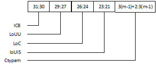
31:30 |
ICB |
RO |
Inner cache boundary. This field indicates the boundary between inner and outer domain. The possible values of this field are:
|
29:27 |
LoUU |
RO |
Level of Unification Uniprocessor. This field indicates the Level of Unification Uniprocessor for the cache hierarchy. |
26:24 |
LoC |
RO |
Level of Coherence. This field indicates the Level of Coherence for the cache hierarchy. |
23:21 |
LoUIS |
RO |
Level of Unification Inner Shareable. This field indicates the Level of Unification Shareable for the cache hierarchy. |
3(m-1)+2:3(m-1) (m = 1 to 7) |
Ctypem |
RO |
Cache type field m. Indicates the type of cache implemented at level m. The possible values of this field are:
All other values are reserved. |
SCB_CTR
The SCB_CTR characteristics are:
Purpose: Provides information about the architecture of the caches.
Usage constraints:
Privileged access permitted only. Unprivileged accesses generate a fault.
This register is word accessible only. Half-word and byte accesses are UNPREDICTABLE.
From Armv8.1-M, this register is accessible to accesses through unprivileged DAP requests when either DAUTHCTRL_S.UIDAPEN or DAUTHCTRL_NS.UIDAPEN is set.
Configurations: This register is always implemented.
Attributes:
32-bit read-only register located at 0xE000_ED7C.
Secure software can access the Non-secure version of this register via CTR_NS located at 0xE002_ED7C.
The location 0xE002_ED7C is RES0 to software executing in Non-secure state and the debugger.
This register is banked between Security states.
Default value: 0x8303_C003
Bit |
Symbol |
Access |
Description |
|---|---|---|---|
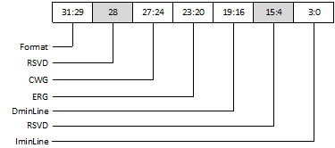
31:29 |
Format |
RO |
Cache Type Register format. Indicates whether cache type information is provided. The possible values of this field are:
|
28 |
RSVD |
Reserved |
|
27:24 |
CWG |
RO |
Cache Write-Back Granule. Log2 of the number of words of the maximum size of memory that can be overwritten as a result of the eviction of a cache entry that has had a memory location in it modified. The possible values of this field are:
|
23:20 |
ERG |
RO |
Exclusives Reservation Granule. Log2 of the number of words of the maximum size of the reservation granule that has been implemented for the Load-Exclusive and Store-Exclusive instructions. The possible values of this field are:
|
19:16 |
DminLine |
RO |
Data cache minimum line length. Log2 of the number of words(4 bytes) in the smallest cache line of all the data caches and unified caches that are controlled by the PE. |
15:4 |
RSVD |
Reserved |
|
3:0 |
IminLine |
RO |
Instruction cache minimum line length. Log2 of the number of words in the smallest cache line of all the instruction caches that are controlled by the PE. |
SCB_CCSIDR
The CCSIDR characteristics are:
Purpose: The CCSIDR provides information about the architecture of the currently selected cache.
Usage constraints:
Privileged access permitted only. Unprivileged accesses generate a fault.
This register is word accessible only. Half-word and byte accesses are UNPREDICTABLE.
From Armv8.1-M, this register is accessible to accesses through unprivileged DAP requests when either DAUTHCTRL_S.UIDAPEN or DAUTHCTRL_NS.UIDAPEN is set.
If CSSELR points to an unimplemented cache, the value of this register is UNKNOWN.
Configurations: This register is always implemented.
Attributes:
32-bit read-only register located at 0xE000_ED80.
Secure software can access the Non-secure version of this register via CCSIDR_NS located at 0xE002_ED80.
The location 0xE002_ED80 is RES0 to software executing in Non-secure state and the debugger.
This register is banked between Security states.
Preface:
Provides indirect read access to the architecture of the cache currently selected by CSSELR. The parameters NumSets, Associativity, and LineSize in these registers define the architecturally visible parameters that are required for the cache maintenance by Set/Way instructions. They are not guaranteed to represent the actual microarchitectural features of a design. You cannot make any inference about the actual sizes of caches based on these parameters.
Default value:
KM0: D-Cache 0xF00F_E009, I-Cache 0xE01F_E009
KM4: D-Cache 0xF01F_E019, I-Cache 0xE03F_E019
Bit |
Symbol |
Access |
Description |
|---|---|---|---|
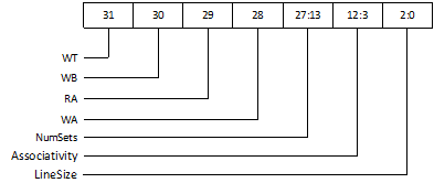
31 |
WT |
RO |
Write-Through. Indicates whether the currently selected cache level supports Write-Through. The possible values of this bit are:
|
30 |
WB |
RO |
Write-Back. Indicates whether the currently selected cache level supports Write-Back. The possible values of this bit are:
|
29 |
RA |
RO |
Read-Allocation. Indicates whether the currently selected cache level supports Read-Allocation. The possible values of this bit are:
|
28 |
WA |
RO |
Write-Allocation. Indicates whether the currently selected cache level supports Write-Allocation. The possible values of this bit are:
|
27:13 |
NumSets |
RO |
Number of sets. Indicates (number of sets in the currently selected cache) - 1. Therefore, a value of 0 indicates that 1 set in the cache. The number of sets does not have to be a power of 2. |
12:3 |
Associativity |
RO |
Associativity. Indicates (the associativity of cache) - 1. A value of 0 indicates an associativity of 1. The associativity does not have to be a power of 2. |
2:0 |
LineSize |
RO |
Line size. Indicates (log2(number of words per line in the currently selected cache)) - 2. |
SCB_CSSELR
The SCB_CSSELR characteristics are:
Purpose: Selects the current Cache Size ID Register, CCSIDR, by specifying the required cache level and the cache type (either instruction or data cache)
Usage constraints:
Privileged access permitted only. Unprivileged accesses generate a fault.
This register is word accessible only. Half-word and byte accesses are UNPREDICTABLE.
From Armv8.1-M, this register is accessible to accesses through unprivileged DAP requests when either DAUTHCTRL_S.UIDAPEN or DAUTHCTRL_NS.UIDAPEN is set.
Configurations: This register is always implemented.
Attributes:
32-bit read/write register located at 0xE000_ED84.
Secure software can access the Non-secure version of this register via CSSELR_NS located at 0xE002_ED84.
The location 0xE002_ED84 is RES0 to software executing in Non-secure state and the debugger.
This register is banked between Security states.
From Armv8.1-M onwards it is IMPLEMENTATION DEFINED whether a debugger write to this register is ignored when the PE is not in Debug state.
Bit |
Symbol |
Access |
Description |
|---|---|---|---|
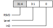
31:4 |
RSVD |
Reserved |
|
3:1 |
Level |
R/W |
Cache level. Selects which cache level is to be identified. Permitted values are from 0b000, indicating Level 1 cache, to 0b110 indicating Level 7 cache. The possible values of this field are:
|
0 |
InD |
R/W |
Instruction not data. Selects whether the instruction or the data cache is to be identified. The possible values of this bit are:
|
SCB_ICIALLU
The SCB_ICIALLU characteristics are:
Purpose: Invalidate all instruction caches to PoU.
Usage constraints:
Privileged access permitted only. Unprivileged accesses generate a fault.
This register is word accessible only. Half-word and byte accesses are UNPREDICTABLE.
From Armv8.1-M, this register is accessible to accesses through unprivileged DAP requests when either DAUTHCTRL_S.UIDAPEN or DAUTHCTRL_NS.UIDAPEN is set.
Configurations: This register is always implemented.
Attributes:
32-bit write-only register located at 0xE000_EF50.
Secure software can access the Non-secure version of this register via ICIALLU_NS located at 0xE002_EF50.
The location 0xE002_EF50 is RES0 to software executing in Non-secure state and the debugger.
This register is not banked between Security states.
Bit |
Symbol |
Access |
Description |
|---|---|---|---|
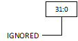
31:0 |
IGNORED |
WO |
The value written to this field is ignored. Ignored. |
SCB_ICIMVAU
The SCB_ICIMVAU characteristics are:
Purpose: Invalidate instruction cache line by address to PoU.
Usage constraints:
Privileged access permitted only. Unprivileged accesses generate a fault.
This register is word accessible only. Half-word and byte accesses are UNPREDICTABLE.
From Armv8.1-M, this register is accessible to accesses through unprivileged DAP requests when either DAUTHCTRL_S.UIDAPEN or DAUTHCTRL_NS.UIDAPEN is set.
Configurations: This register is always implemented.
Attributes:
32-bit write-only register located at 0xE000EF58.
Secure software can access the Non-secure version of this register via ICIMVAU_NS located at 0xE002_EF58. The location 0xE002_EF58 is RES0 to software executing in Non-secure state and the debugger.
This register is not banked between Security states.
Bit |
Symbol |
Access |
Description |
|---|---|---|---|
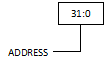
31:0 |
ADDRESS |
WO |
Address. Writing to this field initiates the maintenance operation for the address written. |
SCB_DCIMVAC
The DCIMVAC characteristics are:
Purpose: Invalidate data or unified cache line by address to PoC.
Usage constraints:
Privileged access permitted only. Unprivileged accesses generate a fault.
This register is word accessible only. Half-word and byte accesses are UNPREDICTABLE.
Configurations: This register is always implemented.
Attributes:
32-bit write-only register located at 0xE000_EF5C.
Secure software can access the Non-secure version of this register via DCIMVAC_NS located at 0xE002_EF5C. The location 0xE002_EF5C is RES0 to software executing in Non-secure state and the debugger.
This register is not banked between Security states.

Bit |
Symbol |
Access |
Description |
|---|---|---|---|
31:0 |
ADDRESS |
WO |
Address. Writing to this field initiates the maintenance operation for the address written. |
SCB_DCISW
The SCB_DCISW characteristics are:
Purpose: Invalidate data or unified cache line by set/way.
Usage constraints:
Privileged access permitted only. Unprivileged accesses generate a fault.
This register is word accessible only. Half-word and byte accesses are UNPREDICTABLE.
Configurations: This register is always implemented.
Attributes:
32-bit write-only register located at 0xE000_EF60.
Secure software can access the Non-secure version of this register via DCISW_NS located at 0xE002_EF60.
The location 0xE002_EF60 is RES0 to software executing in Non-secure state and the debugger.
This register is not banked between Security states.
Bit |
Symbol |
Access |
Description |
|---|---|---|---|
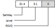
31:4 |
SetWay |
WO |
Cache set/way. Contains two fields:
Bits[L-1:4] are RES0. A = Log2(ASSOCIATIVITY), L = Log2(LINELEN), B = (L + S), S = Log2(NSETS). ASSOCIATIVITY, LINELEN (line length, in bytes), and NSETS (number of sets) have their usual meanings and are the values for the cache level being operated on. The values of A and S are rounded up to the next integer. |
3:1 |
Level |
WO |
Cache level. Cache level to operate on, minus 1. For example, this field is 0 for operations on L1 cache, or 1 for operations on L2 cache. |
0 |
RSVD |
Reserved |
SCB_DCCMVAU
The SCB_DCCMVAU characteristics are:
Purpose: Clean data or unified cache line by address to PoU.
Usage constraints:
Privileged access permitted only. Unprivileged accesses generate a fault.
This register is word accessible only. Half-word and byte accesses are UNPREDICTABLE.
From Armv8.1-M, this register is accessible to accesses through unprivileged DAP requests when either DAUTHCTRL_S.UIDAPEN or DAUTHCTRL_NS.UIDAPEN is set.
Configurations: This register is always implemented.
Attributes:
32-bit write-only register located at 0xE000_EF64.
Secure software can access the Non-secure version of this register via DCCMVAU_NS located at 0xE002_EF64. The location 0xE002_EF64 is RES0 to software executing in Non-secure state and the debugger.
This register is not banked between Security states.

Bit |
Symbol |
Access |
Description |
|---|---|---|---|
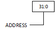
31:0 |
ADDRESS |
WO |
Address. Writing to this field initiates the maintenance operation for the address written. |
SCB_DCCMVAC
The SCB_DCCMVAC characteristics are:
Purpose: Clean data or unified cache line by address to PoC.
Usage constraints:
Privileged access permitted only. Unprivileged accesses generate a fault.
This register is word accessible only. Half-word and byte accesses are UNPREDICTABLE.
From Armv8.1-M, this register is accessible to accesses through unprivileged DAP requests when either DAUTHCTRL_S.UIDAPEN or DAUTHCTRL_NS.UIDAPEN is set.
Configurations: This register is always implemented.
Attributes:
32-bit write-only register located at 0xE000_EF68.
Secure software can access the Non-secure version of this register via DCCMVAC_NS located at 0xE002_EF68. The location 0xE002_EF68 is RES0 to software executing in Non-secure state and the debugger.
This register is not banked between Security states.

Bit |
Symbol |
Access |
Description |
|---|---|---|---|
31:0 |
ADDRESS |
WO |
Address. Writing to this field initiates the maintenance operation for the address written. |
SCB_DCCSW
The SCB_DCCSW characteristics are:
Purpose: Clean data or unified cache line by set/way.
Usage constraints:
Privileged access permitted only. Unprivileged accesses generate a fault.
This register is word accessible only. Half-word and byte accesses are UNPREDICTABLE.
From Armv8.1-M, this register is accessible to accesses through unprivileged DAP requests when either DAUTHCTRL_S.UIDAPEN or DAUTHCTRL_NS.UIDAPEN is set.
Configurations: This register is always implemented.
Attributes:
32-bit write-only register located at 0xE000_EF6C.
Secure software can access the Non-secure version of this register via DCCSW_NS located at 0xE002_EF6C.
The location 0xE002_EF6C is RES0 to software executing in Non-secure state and the debugger.
This register is not banked between Security states.

Bit |
Symbol |
Access |
Description |
|---|---|---|---|
31:4 |
SetWay |
WO |
Cache set/way. Contains two fields:
Bits [L-1:4] are RES0. A = Log2(ASSOCIATIVITY), L = Log2(LINELEN), B = (L + S), S = Log2(NSETS). ASSOCIATIVITY, LINELEN (line length, in bytes), and NSETS (number of sets) have their usual meanings and are the values for the cache level being operated on. The values of A and S are rounded up to the next integer. |
3:1 |
Level |
WO |
Cache level. Cache level to operate on, minus 1. For example, this field is 0 for operations on L1 cache, or 1 for operations on L2 cache. |
0 |
RSVD |
Reserved |
SCB_DCCIMVAC
The SCB_DCCIMVAC characteristics are:
Purpose: Clean and invalidate data or unified cache line by address to PoC.
Usage constraints:
Privileged access permitted only. Unprivileged accesses generate a fault.
This register is word accessible only. Half-word and byte accesses are UNPREDICTABLE.
From Armv8.1-M, this register is accessible to accesses through unprivileged DAP requests when either DAUTHCTRL_S.UIDAPEN or DAUTHCTRL_NS.UIDAPEN is set.
Configurations: This register is always implemented.
Attributes:
32-bit write-only register located at 0xE000_EF70.
Secure software can access the Non-secure version of this register via DCCIMVAC_NS located at 0xE002_EF70. The location 0xE002_EF70 is RES0 to software executing in Non-secure state and the debugger.
This register is not banked between Security states.
Bit |
Symbol |
Access |
Description |
|---|---|---|---|
31:0 |
ADDRESS |
WO |
Address. Writing to this field initiates the maintenance operation for the address written. |
SCB_DCCISW
The SCB_DCCISW characteristics are:
Purpose: Clean and invalidate data or unified cache line by set/way.
Usage constraints:
Privileged access permitted only. Unprivileged accesses generate a fault.
This register is word accessible only. Half-word and byte accesses are UNPREDICTABLE.
From Armv8.1-M, this register is accessible to accesses through unprivileged DAP requests when either DAUTHCTRL_S.UIDAPEN or DAUTHCTRL_NS.UIDAPEN is set.
Configurations: This register is always implemented.
Attributes:
32-bit write-only register located at 0xE000_EF74.
Secure software can access the Non-secure version of this register via DCCISW_NS located at 0xE002_EF74.
The location 0xE002_EF74 is RES0 to software executing in Non-secure state and the debugger.
This register is not banked between Security states.

Bit |
Symbol |
Access |
Description |
|---|---|---|---|
31:4 |
SetWay |
WO |
Cache set/way. Contains two fields:
Bits [L-1:4] are RES0. A = Log2(ASSOCIATIVITY), L = Log2(LINELEN), B = (L + S), S = Log2(NSETS). ASSOCIATIVITY, LINELEN (line length, in bytes), and NSETS (number of sets) have their usual meanings and are the values for the cache level being operated on. The values of A and S are rounded up to the next integer. |
3:1 |
Level |
WO |
Cache level. Cache level to operate on, minus 1. For example, this field is 0 for operations on L1 cache, or 1 for operations on L2 cache. |
0 |
RSVD |
Reserved |
ACTLR
The ACTLR characteristics are:
Purpose: Provides IMPLEMENTATION DEFINED configuration and control options.
Usage constraints:
Privileged access permitted only. Unprivileged accesses generate a fault.
This register is word accessible only. Half-word and byte accesses are UNPREDICTABLE.
Configurations: This register is always implemented.
Attributes:
32-bit read/write register located at 0xE000_E008.
Secure software can access the Non-secure version of this register via ACTLR_NS located at 0xE002_E008.
The location 0xE002_E008 is RES0 to software executing in Non-secure state and the debugger.
It is IMPLEMENTATION DEFINED whether this register is banked between Security states.
From Armv8.1-M onwards it is IMPLEMENTATION DEFINED whether a debugger write to this register is ignored when the PE is not in Debug state.
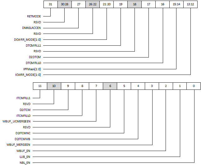
Bit |
Symbol |
Access |
Description |
|---|---|---|---|
31 |
RETMODE |
RO |
Indicates the core is reset from retention mode or not.
Reset value is controlled by the input pin in retention mode. |
30:28 |
RSVD |
Reserved |
|
27 |
DMASLACCEN |
R/W |
DMA in sleep enable.
Reset value is 0. RAZ/WI if EXT_DMA==NO |
26:22 |
RSVD |
Reserved |
|
21:20 |
DCWRR_MODE[1:0] |
R/W |
Data Cache Way Restricted Operation Mode Reset value is 2’b11. RAZ/WI if DCACHE==NONE |
19 |
DTCMFILL1 |
WO |
Writing 1 to this bit triggers the core to fill its DTCM1. Writing 0 has no effect. |
18 |
RSVD |
Reserved |
|
17 |
D2DTCM |
R/W |
Instruction fetch from DTCM enable. The reset value is derived from INITD2DTCM pin. |
16 |
DTCMFILL0 |
WO |
Writing 1 to this bit triggers the core to fill its DTCM. Writing 0 has no effect. |
15:14 |
IPFMask[1:0] |
R/W |
ISide prefetch number.
|
13:12 |
ICWRR_MODE[1:0] |
R/W |
Instruction Cache Way Restricted Operation Mode Reset value is 2’b11. RAZ/WI if ICACHE==NONE |
11 |
ITCMFILL1 |
WO |
Writing 1 to this bit triggers the core to fill its ITCM1. Writing 0 has no effect. |
10 |
RSVD |
Reserved |
|
9 |
D2ITCM |
R/W |
Data load store to and from ITCM enable. The reset value is derived from INITD2ITCM pin. |
8 |
ITCMFILL0 |
WO |
Writing 1 to this bit triggers the core to fill its ITCM. Writing 0 has no effect. |
7 |
WBUF_UCMERGEEN |
R/W |
Write buffer merge enable for uncacheable requests
Reset value is 0. |
6 |
RSVD |
Reserved |
|
5 |
D2ITCMNC |
R/W |
Data load store request hits ITCM is forced to be non-cacheable.
Reset value is 0. |
4 |
D2ITCMWB |
R/W |
Data load store request hits ITCM is forced to be write-back.
Reset value is 0. |
3 |
WBUF_MERGEEN |
R/W |
Write buffer merge enable.
Reset value is 1. |
2 |
WBUF_EN |
R/W |
Write buffer enable.
Reset value is 1. |
1 |
LUB_EN |
R/W |
Load-use date buffer enable.
Reset value is 1. |
0 |
NBL_EN |
R/W |
Non-blocking load enable.
Reset value is 1. |
When data cache is 4-way associated:
DCWRR_MODE[1:0] |
Data in restricted range |
Data not in restrict range |
|---|---|---|
2’b00 |
Uses way 0 |
Uses way 1, way 2, and way 3 |
2’b01 |
Uses way 0 and way 1 |
Uses way 2 and way 3 |
2’b10 |
Uses way 0, way 1, and way2 |
Uses way 3 |
2’b11 |
Uses all ways |
Uses no ways |
When data cache is 2-way associated:
DCWRR_MODE[1:0] |
Data in restricted range |
Data not in restrict range |
|---|---|---|
2’bz0 |
Uses way 0 |
Uses way 1 |
2’bz1 |
Uses all ways |
Uses no ways |
When instruction cache is 4-way associated:
ICWRR_MODE[1:0] |
Data in restricted range |
Data not in restrict range |
|---|---|---|
2’b00 |
Uses way 0 |
Uses way 1, way 2, and way 3 |
2’b01 |
Uses way 0 and way 1 |
Uses way 2 and way 3 |
2’b10 |
Uses way 0, way 1, and way 2 |
Uses way 3 |
2’b11 |
Uses all ways |
Uses no ways |
When instruction cache is 2-way associated:
ICWRR_MODE[1:0] |
Data in restricted range |
Data not in restrict range |
|---|---|---|
2’bz0 |
Uses way 0 |
Uses way 1 |
2’bz1 |
Uses all ways |
Uses no ways |
ICWRR_BASE
The ICWRR_BASE characteristics are:
Purpose: Provides Instruction Cache Way Restricted Range base.
Usage constraints:
Privileged access permitted only. Unprivileged accesses generate a fault.
This register is word accessible only. Half-word and byte accesses are UNPREDICTABLE.
Attributes:
32-bit read/write register located at 0xE00420A0.
This register can only be accessed from privileged requests, and is RAZ/WI from Secure State if a security extension presents.
Default value: 0x0000_0000

Bit |
Symbol |
Access |
Description |
|---|---|---|---|
31:16 |
RESTRICTED_RANGE_BASE |
R/W |
Indicates Way Restricted Range Base Address.(65536 bytes alignment) |
15:0 |
RSVD |
Reserved |
ICWRR_TOP
The ICWRR_TOP characteristics are:
Purpose: Provides Instruction Cache Way Restricted Range Top.
Usage constraints:
Privileged access permitted only. Unprivileged accesses generate a fault.
This register is word accessible only. Half-word and byte accesses are UNPREDICTABLE.
Attributes:
32-bit read/write register located at 0xE004_20A4.
This register can only be accessed from privileged request, and is RAZ/WI from Secure State if security extension presents.
Default value: 0xFFFF_0000

Bit |
Symbol |
Access |
Description |
|---|---|---|---|
31:16 |
RESTRICTED_RANGE_TOP |
R/W |
Indicates Way Restricted Range TOP Address.(65536 bytes alignment) |
15:0 |
RSVD |
Reserved |
DCWRR_BASE
The DCWRR_BASE characteristics are:
Purpose: Provides Data Cache Way Restricted Range base.
Usage constraints:
Privileged access permitted only. Unprivileged accesses generate a fault.
This register is word accessible only. Half-word and byte accesses are UNPREDICTABLE.
Attributes:
32-bit read/write register located at 0xE004_20A8.
This register can only be accessed from privileged request, and is RAZ/WI from Secure State if security extension presents.
Default value: 0x0000_0000
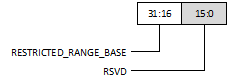
Bit |
Symbol |
Access |
Description |
|---|---|---|---|
31:16 |
RESTRICTED_RANGE_BASE |
R/W |
Indicates Way Restricted Range Base Address (65536 bytes alignment) |
15:0 |
RSVD |
Reserved |
DCWRR_TOP
The DCWRR_TOP characteristics are:
Purpose: Provides Data Cache Way Restricted Range Top.
Usage constraints:
Privileged access permitted only. Unprivileged accesses generate a fault.
This register is word accessible only. Half-word and byte accesses are UNPREDICTABLE.
Attributes:
32-bit read/write register located at 0xE004_20AC.
This register can only be accessed from privileged request, and is RAZ/WI from Secure State if security extension presents.
Default value: 0xFFFF_0000
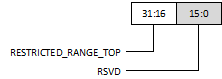
Bit |
Symbol |
Access |
Description |
|---|---|---|---|
31:16 |
RESTRICTED_RANGE_TOP |
R/W |
Indicates Way Restricted Range TOP Address (65536 bytes alignment) |
15:0 |
RSVD |
Reserved |
DTCM0_BASE
The DTCM0_BASE characteristics are:
Purpose: Provides DTCM0 Range Base.
Usage constraints:
Privileged access permitted only. Unprivileged accesses generate a fault.
This register is word accessible only. Half-word and byte accesses are UNPREDICTABLE.
Attributes:
32-bit read/write register located at 0xE004_2060.
This register can only be accessed from privileged request, and is RAZ/WI from Secure State if security extension presents.
Default value: 0x0008_0000
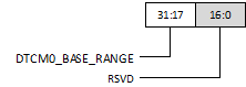
Bit |
Symbol |
Access |
Description |
|---|---|---|---|
31:17 |
DTCM0_BASE_RANGE |
R/W |
Indicates DTCM0 Range Base, aligned at 1K bytes. |
16:0 |
RSVD |
RO |
Reserved |
DTCM0_TOP
The DTCM0_TOP characteristics are:
Purpose: Provides DTCM0 Range Top.
Usage constraints:
Privileged access permitted only. Unprivileged accesses generate a fault.
This register is word accessible only. Half-word and byte accesses are UNPREDICTABLE.
Attributes:
32-bit read/write register located at 0xE004_2064.
This register can only be accessed from privileged request, and is RAZ/WI from Secure State if security extension presents.
Default value: 0x0009_7FFF
Bit |
Symbol |
Access |
Description |
|---|---|---|---|
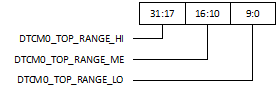
31:17 |
DTCM0_TOP_RANGE_HI |
RO |
Higher bits of the DTCM0_TOP register. The value is the same with DTCM0_BASE[31:17]. |
16:10 |
DTCM0_TOP_RANGE_ME |
R/W |
Medium bits of the DTCM0_TOP register. The reset value is the bit[16:10] of the DTCM0_TOP register set in the configuration form. |
9:0 |
DTCM0_TOP_RANGE_LO |
RO |
Lower bits of the DTCM0_TOP register. The value is 10’h3ff. |
Not supported.
