Bus Architecture
Introduction
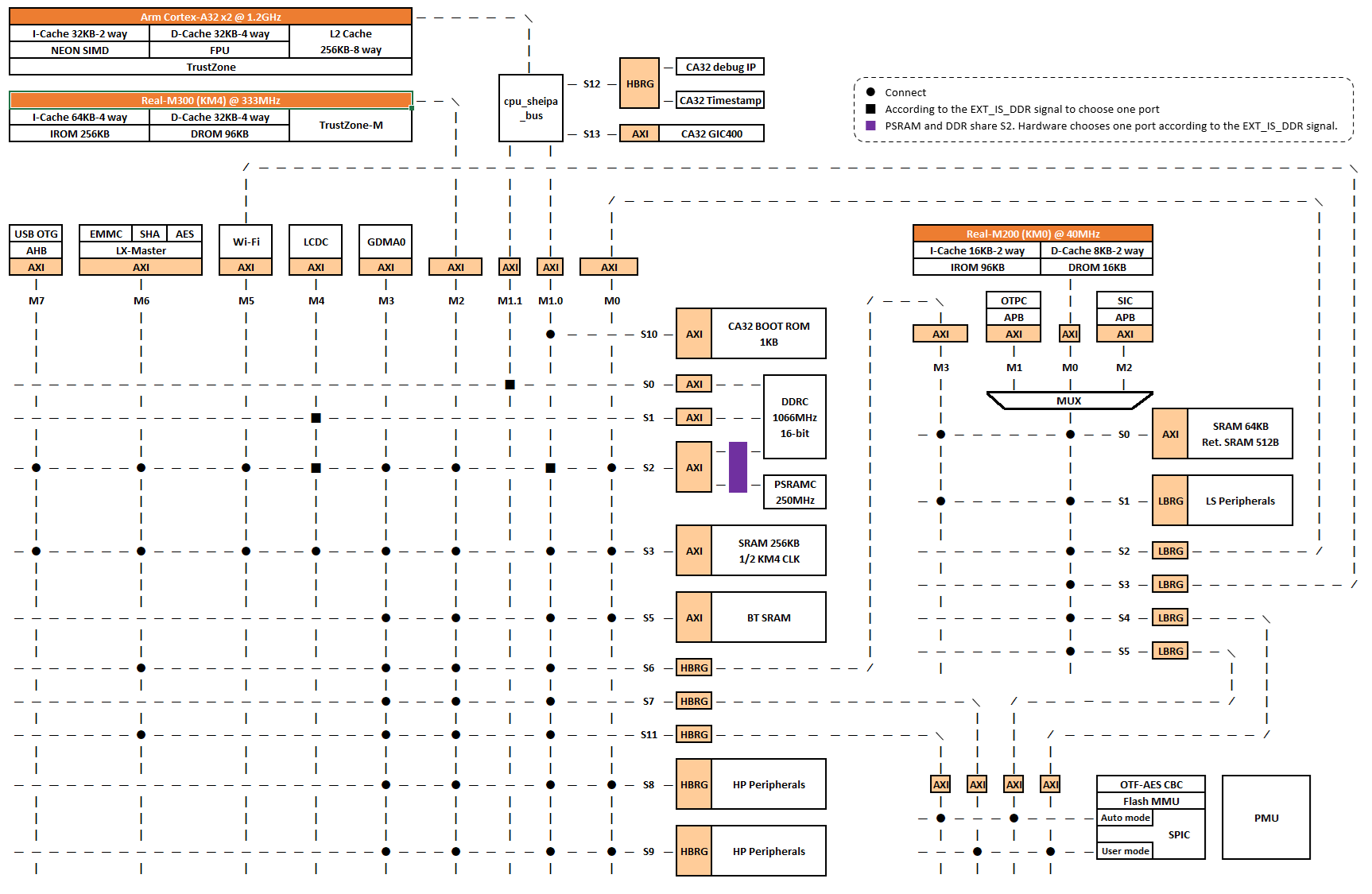
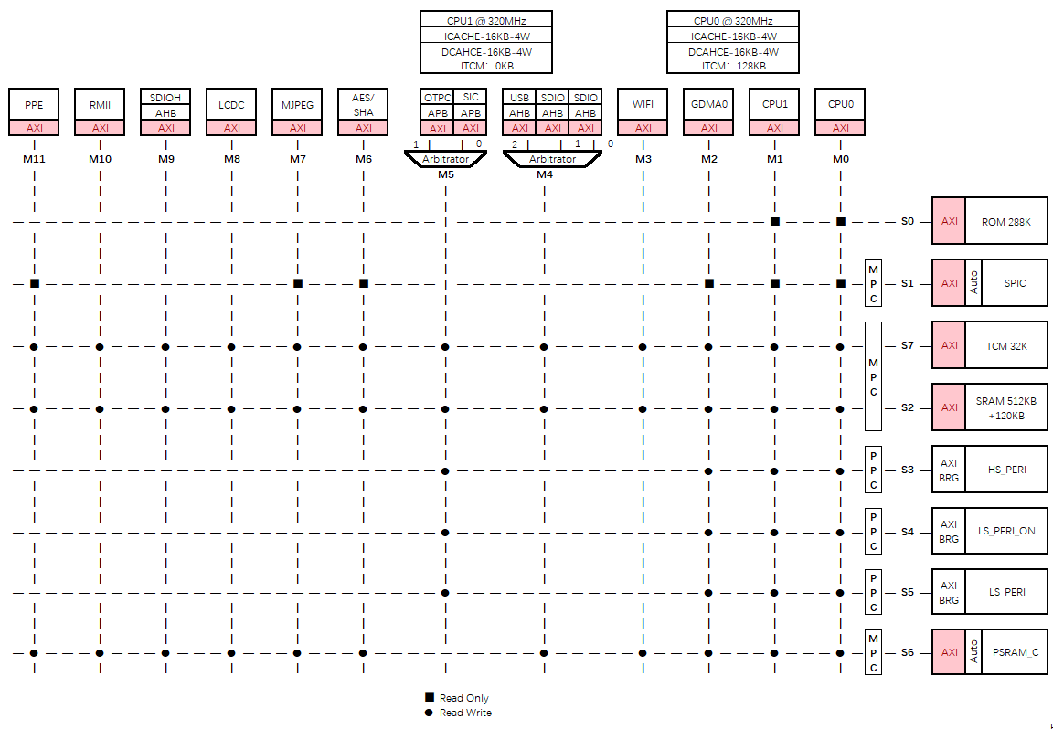
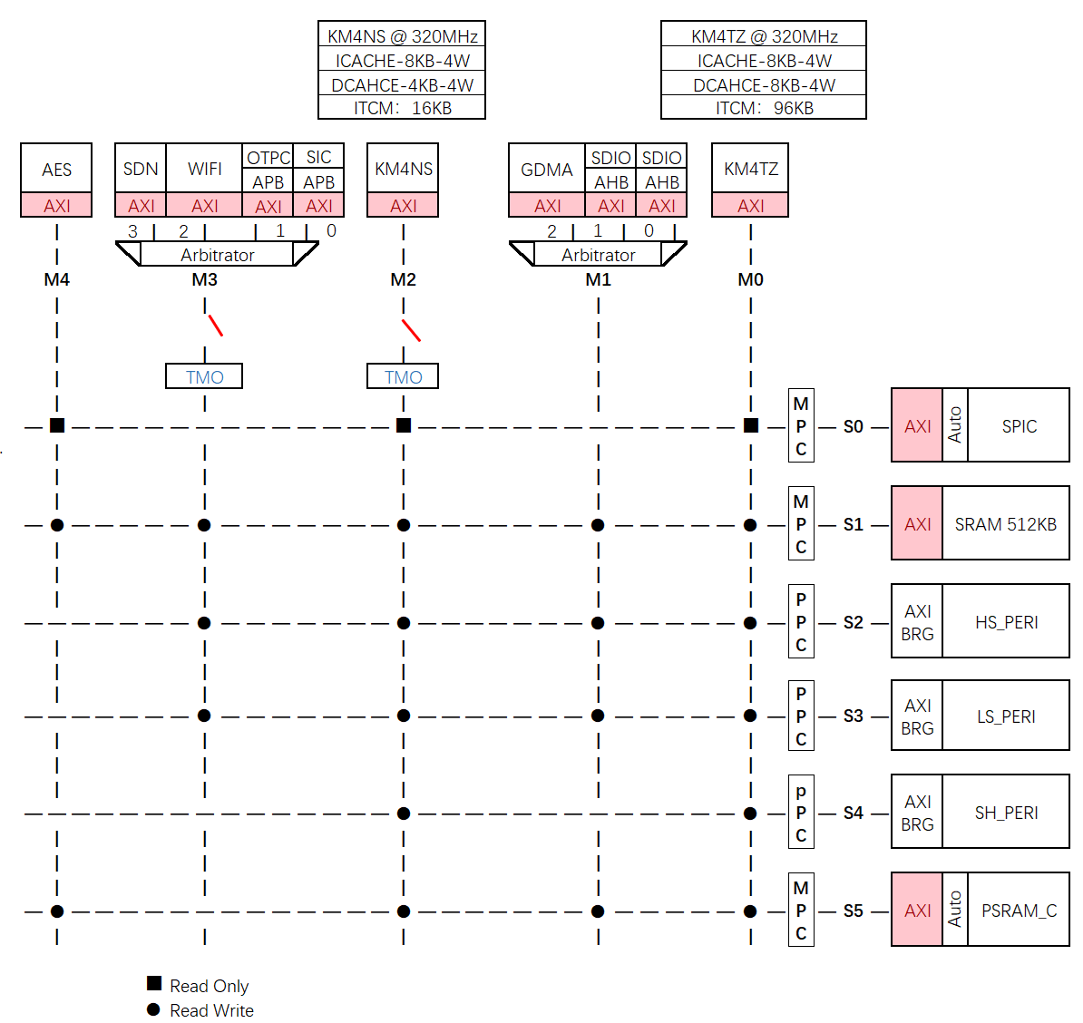
The chip uses a Multi-layer AXI Matrix as its on-chip communication bus architecture. This can be understood as a “multi-lane interchange hub” inside the chip: multiple Masters (modules that initiate transfers, such as CPUs and DMAs) can simultaneously access Slaves (target modules being accessed, such as SRAM, Flash, and peripherals) through different paths without interference. Its key features are as follows:
Multi-channel Parallel Access: Multiple Masters can simultaneously access different Slaves through different paths, eliminating the serial bottleneck of traditional single-bus architectures and significantly improving data throughput.
Hierarchical Peripheral Integration: The high-speed AXI matrix directly connects CPUs and memories, while low-speed peripherals (APB4) are connected through dedicated AXI-to-AHB/APB bridges at reduced speeds, ensuring that the high-speed core is not slowed down by waiting for slow peripherals.
Note
The ARM AMBA bus protocols are divided into three tiers by performance: AXI4 (high-speed, used for CPU/DMA/memory), AHB (medium-speed, commonly used for bus bridges), and APB4 (low-speed, used for peripheral register access).
Architecture Diagram
The bus architecture of each chip is shown in the figures below. The figures illustrate how each master port (M*) connects to each slave port (S*) through the interconnect matrix, as well as the hierarchical positions of AXI/AHB/APB4 bridges.
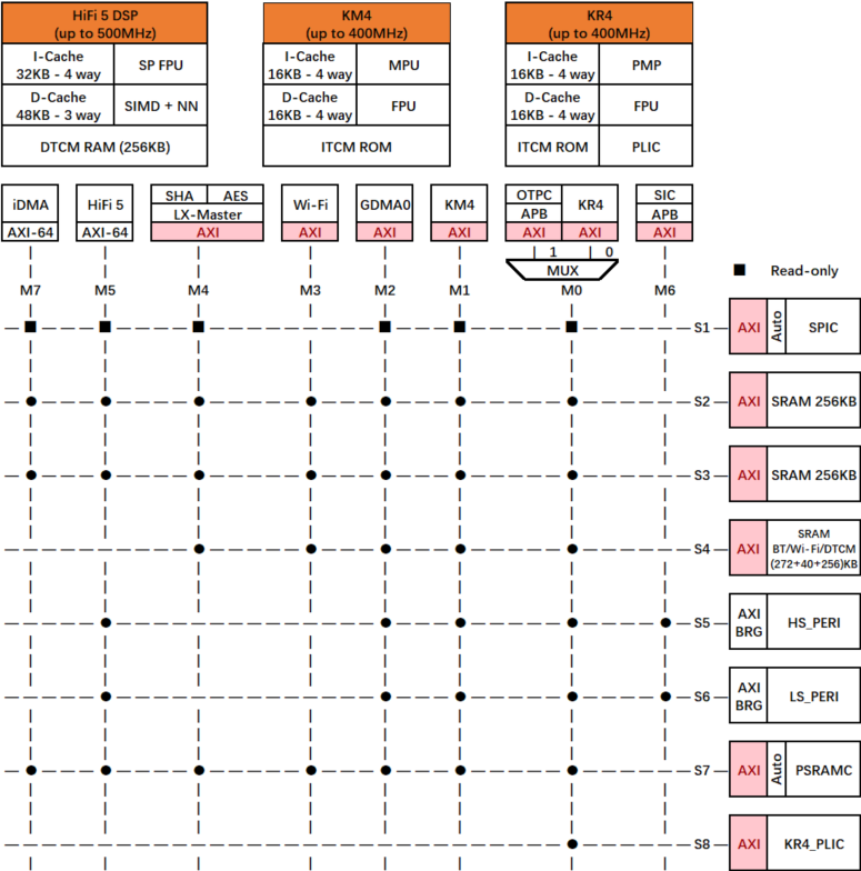
Master Ports
Master Ports are the initiating side of bus transactions. Modules that need to actively read and write data — such as CPUs, DMAs, and Wi-Fi — connect to the interconnect matrix through master ports.
Port ID |
Master |
Interconnect type |
Data bus width |
Description |
|---|---|---|---|---|
M0 |
KM0 |
AXI4 |
32 bits |
KM0 CPU master |
M1 |
KM4 |
AXI4 |
32 bits |
KM4 CPU master |
M2 |
GDMA0 |
AXI4 |
32 bits |
GDMA0 controller master |
M3 |
Wi-Fi |
AXI4 |
32 bits |
Wi-Fi master |
M4-0 |
SDIO |
AHB |
32 bits |
SDIO master |
M4-1 |
LX_Master_AES_Hash |
AXI4 |
32 bits |
AES/SHA master |
M5-0 |
SIC |
APB4 |
32 bits |
SIC master |
M5-1 |
OTPC |
APB4 |
32 bits |
OTP controller master |
M6 |
PPE |
AXI4 |
32 bits |
PPE master |
Port ID |
Master |
Interconnect type |
Data bus width |
Description |
|---|---|---|---|---|
M0-0 |
KR4 |
AXI4 |
32 bits |
KR4 CPU master |
M0-1 |
OTPC |
APB4 |
32 bits |
OTP controller master |
M1 |
KM4 |
AXI4 |
32 bits |
KM4 CPU master |
M2 |
GDMA0 |
AXI4 |
32 bits |
GDMA0 controller master |
M3 |
Wi-Fi |
AXI4 |
32 bits |
Wi-Fi master |
M4 |
LX_Master |
AXI4 |
32 bits |
AES/SHA master |
M6 |
SIC |
APB4 |
32 bits |
SIC master |
Port ID |
Master |
Interconnect type |
Data bus width |
Description |
|---|---|---|---|---|
M0-0 |
KR4 |
AXI4 |
32 bits |
KR4 CPU master |
M0-1 |
OTPC |
APB4 |
32 bits |
OTP controller master |
M1 |
KM4 |
AXI4 |
32 bits |
KM4 CPU master |
M2 |
GDMA0 |
AXI4 |
32 bits |
GDMA0 controller master |
M3 |
Wi-Fi |
AXI4 |
32 bits |
Wi-Fi master |
M4 |
LX_Master |
AXI4 |
32 bits |
AES/SHA master |
M5 |
HiFi 5 DSP |
AXI4 |
64 bits |
HiFi 5 DSP master |
M6 |
SIC |
APB4 |
32 bits |
SIC master |
M7 |
iDMA |
AXI4 |
64 bits |
DSP internal DMA master |
Master Ports of HP Platform
Port ID |
Master |
Interconnect type |
Data bus width |
Description |
|---|---|---|---|---|
M0 |
LS Master Bridge |
AXI |
32 bits |
KM0 CPU master connected to HP matrix through LBRG |
M1 |
CA32 CPU |
AXI |
128 bits |
CA32 CPU master |
M2 |
KM4 CPU |
AXI |
64 bits |
KM4 CPU master |
M3 |
GDMA0 |
AXI |
32 bits |
GDMA0 controller master |
M4 |
LCDC |
AXI |
32 bits |
LCDC master |
M5 |
Wi-Fi |
AXI |
32 bits |
Wi-Fi master |
M6 |
LX_Master |
AXI |
32 bits |
AES/SHA/EMMC master |
M7 |
USB OTG |
AHB |
32 bits |
USB OTG master |
Master Ports of LS Platform
Port ID |
Master |
Interconnect type |
Data bus width |
Description |
|---|---|---|---|---|
M0 |
KM0 CPU |
AXI |
32 bits |
KM0 CPU master |
M1 |
OTPC |
APB |
32 bits |
OTP controller master |
M2 |
SIC |
AHB |
32 bits |
SIC master |
M3 |
HP Master Bridge |
AXI |
128 bits |
HP masters connected to LS matrix through HBRG |
Port ID |
Master |
Interconnect type |
Data bus width |
Description |
|---|---|---|---|---|
M0 |
KM4TZ |
AXI4 |
32 bits |
KM4TZ CPU master |
M1 |
KM4NS |
AXI4 |
32 bits |
KM4NS CPU master |
M2 |
GDMA0 |
AXI4 |
32 bits |
GDMA0 controller master |
M3 |
Wi-Fi |
AXI4 |
32 bits |
Wi-Fi master |
M4-0 |
SDIO_WIFI |
AHB |
32 bits |
SDIO Wi-Fi master |
M4-1 |
SDIO_BT |
AHB |
32 bits |
SDIO Bluetooth master |
M4-2 |
USB |
AXI4 |
32 bits |
USB master |
M5-0 |
SIC |
APB4 |
32 bits |
SIC master |
M5-1 |
OTPC |
APB4 |
32 bits |
OTP controller master |
M6 |
AES/SHA |
AXI4 |
32 bits |
AES/SHA master |
M7 |
MJPEG |
AXI4 |
32 bits |
MJPEG master |
M8 |
LCDC |
AXI4 |
32 bits |
LCDC master |
M9 |
SDIOH |
AHB |
32 bits |
SDIOH master |
M10 |
RMII |
AXI4 |
32 bits |
RMII master |
M11 |
PPE |
AXI4 |
32 bits |
PPE master |
Port ID |
Master |
Interconnect type |
Data bus width |
Description |
|---|---|---|---|---|
M0 |
KM4TZ |
AXI4 |
32 bits |
KM4TZ CPU master |
M1-0 |
SDIO_WIFI |
AHB |
32 bits |
SDIO_WIFI master |
M1-1 |
SDIO_BT |
AHB |
32 bits |
SDIO_BT master |
M1-2 |
GDMA0 |
AXI4 |
32 bits |
GDMA0 controller master |
M2 |
KM4NS |
AXI4 |
32 bits |
KM4NS CPU master |
M3-0 |
SIC |
APB4 |
32 bits |
SIC master |
M3-1 |
OTPC |
APB4 |
32 bits |
OTP controller master |
M3-2 |
Wi-Fi |
AXI4 |
32 bits |
Wi-Fi master |
M3-3 |
SDN |
AXI4 |
32 bits |
SDN master |
M4 |
AES |
AXI4 |
32 bits |
AES master |
Slave Ports
Slave Ports are the responding side of bus accesses, where memories and peripherals are attached as slave devices. The “Security Attribute” column in the tables describes the access control mechanism for each port:
MPC (Memory Protection Controller): Controls security/non-secure partitioning of the memory region; only authorized masters can access the corresponding partition.
PPC (Peripheral Protection Controller): Controls access permissions for peripheral registers.
Non-secure: Not subject to security control; all masters can access directly.
Port ID |
Slave Port |
Interconnect type |
Data bus width |
Security |
Description |
|---|---|---|---|---|---|
S0 |
SPIC Auto Mode |
AXI4 |
32 bits |
Non-secure |
Flash auto mode access, connected to the matrix through SPI Flash controller |
S1 |
HS SRAM0 |
AXI4 |
64 bits |
MPC |
On-chip SRAM |
S2 |
HS_SHARE_SRAM |
AXI4 |
32 bits |
MPC |
BT/Wi-Fi shared SRAM, can be used by masters when BT/Wi-Fi is off. |
S3 |
HS Peripherals |
AXI4/AHB/APB4 |
32 bits |
PPC |
High-speed peripherals |
S4 |
LS_ON Peripherals |
APB4 |
32 bits |
PPC |
Low-speed peripherals that remain powered in sleep mode. |
S5 |
LS Peripherals |
APB4 |
32 bits |
PPC |
Low-speed peripherals |
S6 |
PSRAM |
AXI4 |
32 bits |
MPC |
External PSRAM |
Port ID |
Slave Port |
Interconnect type |
Data bus width |
Security |
Description |
|---|---|---|---|---|---|
S1 |
SPIC Auto Mode |
AXI4 |
32 bits |
Non-secure |
Flash auto mode access, connected to the matrix through SPI Flash controller |
S2 |
SRAM0 |
AXI4 |
64 bits |
MPC |
On-chip SRAM 0 |
S3 |
SRAM1 |
AXI4 |
64 bits |
MPC |
On-chip SRAM 1 |
S4 |
SRAM2 |
AXI4 |
32 bits |
Non-secure |
SRAM for BT and Wi-Fi, can be used as shared system RAM when BT or Wi-Fi is not used. |
S5 |
HS Peripherals |
AHB/APB4 |
32 bits |
PPC |
High-speed peripherals |
S6 |
LS Peripherals |
AXI4/AHB/APB4 |
32 bits |
PPC |
Low-speed peripherals |
S7 |
PSRAM |
AXI4 |
32 bits |
MPC |
External PSRAM |
S8 |
KR4_PLIC |
AXI4 |
32 bits |
Non-secure |
KR4 PLIC |
Port ID |
Slave Port |
Interconnect type |
Data bus width |
Description |
|---|---|---|---|---|
S1 |
SPIC Auto Mode |
AXI4 |
32 bits |
Flash auto mode access, connected to the matrix through SPI Flash controller |
S2 |
SRAM0 |
AXI4 |
64 bits |
On-chip SRAM 0 |
S3 |
SRAM1 |
AXI4 |
64 bits |
On-chip SRAM 1 |
S4 |
SRAM2 |
AXI4 |
32 bits |
SRAM for BT and Wi-Fi, can be used as shared system RAM when BT or Wi-Fi is not used. |
S5 |
HS Peripherals |
AHB/APB4 |
32 bits |
High-speed peripherals |
S6 |
LS Peripherals |
AXI4/AHB/APB4 |
32 bits |
Low-speed peripherals |
S7 |
PSRAM |
AXI4 |
32 bits |
External PSRAM |
S8 |
KR4_PLIC |
AXI4 |
32 bits |
KR4 PLIC |
Port ID |
Slave Port |
Interconnect type |
Data bus width |
Security |
Description |
|---|---|---|---|---|---|
S1 |
SPIC Auto Mode |
AXI4 |
32 bits |
Non-secure |
Flash auto mode access, connected to the matrix through SPI Flash controller |
S2 |
SRAM0 |
AXI4 |
64 bits |
MPC |
On-chip SRAM 0 |
S3 |
SRAM1 |
AXI4 |
64 bits |
MPC |
On-chip SRAM 1 |
S4 |
SRAM2 |
AXI4 |
32 bits |
Non-secure |
SRAM for DSP, BT and Wi-Fi, can be used as shared system RAM when any feature of DSP, BT and Wi-Fi is not used. |
S5 |
HS Peripherals |
AHB/APB4 |
32 bits |
PPC |
High-speed peripherals |
S6 |
LS Peripherals |
AXI4/AHB/APB4 |
32 bits |
PPC |
Low-speed peripherals |
S7 |
PSRAM |
AXI4 |
32 bits |
MPC |
External PSRAM |
S8 |
KR4_PLIC |
AXI4 |
32 bits |
Non-secure |
KR4 PLIC |
Port ID |
Slave Port |
Interconnect type |
Data bus width |
Description |
|---|---|---|---|---|
S1 |
SPIC Auto Mode |
AXI4 |
32 bits |
Flash auto mode access, connected to the matrix through SPI Flash controller |
S2 |
SRAM0 |
AXI4 |
64 bits |
On-chip SRAM 0 |
S3 |
SRAM1 |
AXI4 |
64 bits |
On-chip SRAM 1 |
S4 |
SRAM2 |
AXI4 |
32 bits |
SRAM for DSP, BT and Wi-Fi, can be used as shared system RAM when any feature of DSP, BT and Wi-Fi is not used |
S5 |
HS Peripherals |
AHB/APB4 |
32 bits |
High-speed peripherals |
S6 |
LS Peripherals |
AXI4/AHB/APB4 |
32 bits |
Low-speed peripherals |
S7 |
PSRAM |
AXI4 |
32 bits |
External PSRAM |
S8 |
KR4_PLIC |
AXI4 |
32 bits |
KR4 PLIC |
Slave Ports of HP Platform
Port ID |
Slave Port |
Interconnect type |
Data bus width |
Security |
Description |
|---|---|---|---|---|---|
S0 |
DDR P0 |
AXI |
128 bits |
MPC |
DDR slave port only open to CA32 master |
S1 |
DDR P1 |
AXI |
128 bits |
MPC |
DDR slave port only open to LCDC master |
S2 |
DDR/PSRAM |
AXI |
128/32 bits |
MPC |
PSRAM and DDR share S2. Hardware selects which port to access based on the EXT_MEM_IS_DDR signal. |
S3 |
HP SRAM0 |
AXI |
64 bits |
MPC |
SRAM dedicated to HP masters |
S5 |
HP SRAM2 |
AXI |
32 bits |
Non-secure |
SRAM for BT, it can be used by HP masters when BT is off. |
S6 |
KM0 Slaves |
AXI |
32 bits |
Non-secure |
HP masters access the LS bus matrix through this port. |
S7 |
SPIC User Mode |
AXI |
32 bits |
Non-secure |
Flash user mode access, connected to the matrix through SPIC Flash controller |
S8 |
HP Peripherals |
AHB/APB4 |
32 bits |
PPC |
High-speed peripherals |
S9 |
HP Peripherals |
AXI/AHB/APB4 |
32 bits |
PPC |
High-speed peripherals |
S10 |
CA32 Boot ROM |
AXI |
128 bits |
Secure |
ROM dedicated to CA32 masters |
S11 |
SPIC Auto Mode |
AXI |
32 bits |
Non-secure |
Flash auto mode access, connected to the matrix through SPIC Flash controller |
S12 |
CA32 Debug IP / Timestamp |
APB |
32 bits |
Non-secure |
Debug components dedicated to CA32 masters |
S13 |
CA32 GIC400 |
AXI |
32 bits |
Non-secure |
Interrupt controller dedicated to CA32 masters |
Slave Ports of LS Platform
Port ID |
Slave Port |
Interconnect type |
Data bus width |
Security |
Description |
|---|---|---|---|---|---|
S0 |
KM0 SRAM0 |
AXI |
32 bits |
Non-secure |
SRAM dedicated to LS masters |
S1 |
LS Peripherals |
APB4 |
32 bits |
Non-secure |
Low-speed peripherals |
S2 |
KM4 Slaves |
AXI |
32 bits |
Non-secure |
Bridge to HP bus matrix; LS masters access HP-domain slaves through this port, with Master ID forwarded to HP |
S3 |
Wi-Fi FW |
AHB |
32 bits |
Non-secure |
Wi-Fi FW slave port |
S4 |
SPIC User Mode |
AXI |
32 bits |
Non-secure |
SPI Flash controller |
S5 |
SPIC Auto Mode |
AXI |
32 bits |
Non-secure |
Flash auto mode access, connected to the matrix through SPI Flash controller |
Port ID |
Slave Port |
Interconnect type |
Data bus width |
Security |
Description |
|---|---|---|---|---|---|
S0 |
ROM |
AXI4 |
32 bits |
Non-secure |
KM4TZ Internal ROM |
S1 |
SPIC Auto Mode |
AXI4 |
32 bits |
Non-secure |
Flash auto mode access, connected to the matrix through SPI Flash controller |
S2 |
SRAM |
AXI4 |
64 bits |
MPC |
On-chip SRAM |
S3 |
HS Peripherals |
AXI4/AXI/AHB/APB4/APB3 |
32 bits |
PPC |
High-speed peripherals |
S4 |
LS_ON Peripherals |
APB4 |
32 bits |
PPC |
Low-speed peripherals, remain powered in sleep mode |
S5 |
LS Peripherals |
APB4 |
32 bits |
PPC |
Low-speed peripherals |
S6 |
PSRAM |
AXI4 |
32 bits |
MPC |
External PSRAM |
Port ID |
Slave Port |
Interconnect type |
Data bus width |
Security |
Description |
|---|---|---|---|---|---|
S0 |
SPIC Auto Mode |
AXI4 |
32 bits |
Non-secure |
Flash auto mode access, connected to the matrix through SPI Flash controller |
S1 |
HS SRAM0 |
AXI4 |
64 bits |
MPC |
On-chip SRAM |
S2 |
HS Peripherals |
AXI4/AHB/APB4 |
32 bits |
PPC |
High-speed peripherals |
S3 |
LS Peripherals |
APB4 |
32 bits |
PPC |
Low-speed peripherals |
S4 |
SH Peripherals |
APB4 |
32 bits |
PPC |
Super-high-speed peripherals |
S5 |
PSRAM |
AXI4 |
32 bits |
MPC |
External PSRAM |
Note
For detailed contents of each slave port, refer to Memory Organization .
