Reset and Clock Control (RCC)
The RCC module manages the generation of all the clocks, as well as the clock gating and the control of the system and peripheral resets. It provides high flexibility in the choice of clock sources and allows the application of clock ratios to improve power consumption.
Reset Control
Introduction
In chip, there are serval types of resets: POR, EXT_POR, BOR, WDG, SYSRST, and THM reset.
In principle, each module has only one external asynchronous reset input, but may have multiple clock inputs. The synchronized reset signal is generated according to the input clock inside the module.
Reset Diagram
Reset diagram
Reset Types
The following table lists the reset sources and events that can trigger a reset.
Reset type |
Reset signal |
Description |
|---|---|---|
POR |
regu_por |
A regulator power-on reset is generated when power on |
BOR |
regu_bor |
A regulator brownout reset is generated when BOR detected |
EXT_POR |
ext_rstn |
A external power on reset is generated when external power on |
WDG |
wdg_rstb |
A watchdog reset is generated when watchdog timeout |
SYSRST |
sys_rstb |
Generated when CPU controls NVIC reset register |
THM |
thm_rstn |
A thermal reset is generated when abnormal temperature detected |
Reset Domains
Different reset types reset different domains, as shown in Reset diagram.
Regulator Power-on reset (POR) and External CHIP_EN reset (
EXT_POR) can reset the whole chip.System reset is triggered by software. There are masks for system reset, which can mask reset for Wi-Fi, BT, peripherals, and AON domain peripherals.
A watchdog reset is generated when watchdog timeout. Watchdog reset can reset most of the system.
A thermal reset is generated when abnormal temperature detected. The thermal reset can reset the system and IWDG of AON domain.
Clock Control
This section describes the generation of the various clocks used by chip and options of clock source selection.
Clock Tree
The clock tree of chip is shown below. Different clock sources can be used to drive different functions. Each clock source can be switched on or off independently when it is not used, to optimize the power consumption.
Clock Source
The clock sources of chip are listed below. Different clock sources can drive different functions.
Three external oscillator:
XTAL40M: used for peripherals directly or after frequency division.
XTAL20M: used as one optional clock source for UART and LOGUART.
XTAL128K: dedicated for
BT_32Kafter frequency division
Four internal oscillators:
OSC4M: provides 4MHz clock for KM0 or 2MHz clock for peripherals after frequency division.
OSC131K: used for input of SDM and clock for Cap-Touch and Key-Scan.
OSC100K: resides in the AON domain and used to drive the IWDG and AON modules.
SDM_32K:
Four separate PLLs: each of them can be configured with integer or fractional ratios.
PLL_SYS:
300MHz ~ 600MHz, provides clock for KM4, KM0, and high-performance peripherals after frequency division.SPIC_CK: dedicated for SPIC and PSRAM, the same frequency different phase with
PLL_SYS.SPIC_PS_CK: dedicated for SPIC and PSRAM power-saving
One PLL dedicated for Wi-Fi:
320MHz
Registers
System Reset Registers
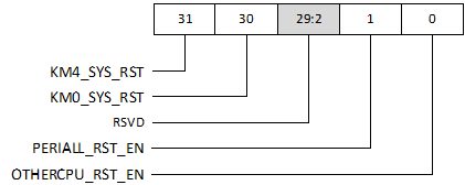
The software needs a way to trigger system reset. A healthy way to implement this function is very important. Two registers are used to implement this function. The base address of system reset registers is 0x4100_8200.
REG_SW_RST_CTRL
Name : Reset Control Register
Size : 32 bits
Address offset : 0x60
Read/write access : read/write
This register can be written when the REG_SW_RST_TRIG register is 0x96969696. The reserved bits in this register may be used to control the reset domain later.

Bit |
Symbol |
Access |
Reset |
Description |
|---|---|---|---|---|
31 |
KM4_SYS_RST |
R/WE/EC |
0 |
KM4 resets the system |
30 |
KM0_SYS_RST |
R/WE/EC |
0 |
KM0 resets the system |
29:2 |
RSVD |
Reserved |
||
1 |
PERIALL_RST_EN |
R/W |
0 |
1: Warm reset request by one CPU will reset all peripherals and local CPU 0: Warm reset request by one CPU will reset local CPU Note: Peripheral reset will also use sysrst mst. |
0 |
OTHERCPU_RST_EN |
R/W |
0 |
1: Warm reset request by one CPU will reset other CPU’s core and local CPU 0: Warm reset request by one CPU will only reset local CPU |
REG_SW_RST_TRIG
Name : Reset Trigger Register
Size : 32 bits
Address offset : 0x64
Read/write access : read/write
The CPU needs to enable the write Reset control permission first by writing 0x96969696 to the REG_SW_RST_TRIG register, and then write the REG_SW_RST_CTRL register, finally write 0x69696969 to trigger the system reset.

Bit |
Symbol |
Access |
Description |
|---|---|---|---|
31:0 |
TRIG_RST |
R/WPD |
System reset trigger register
|
Boot Reason Register
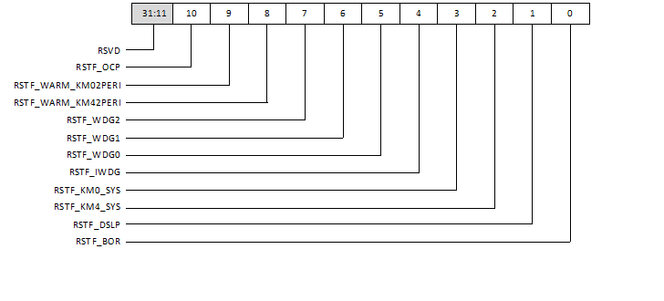
Each time the system boots up, software needs to know if any unexpected event triggered this boot. The boot reason only reflects the latest boot. The base address of this register is 0x4100_8000.
REG_BOOT_REASON_HW
Name : Boot Reason Register
Size : 32 bits
Address offset : 0x20
Read/write access : read

Bit |
Symbol |
Access |
Reset |
Description |
|---|---|---|---|---|
31:11 |
RSVD |
Reserved |
||
10 |
RSTF_OCP |
R/W1CB |
0 |
This bit will be set to 1 when OCP happens, which will let system enter deep-sleep mode. Write 1 to clear. |
9 |
RSTF_WARM_KM02PERI |
R/W1CB |
0 |
This bit will be set to 1 when KM0 warm resets the system. Write 1 to clear. |
8 |
RSTF_WARM_KM42PERI |
R/W1CB |
0 |
This bit will be set to 1 when KM4 warm resets the system. Write 1 to clear. |
7 |
RSTF_WDG2 |
R/W1CB |
0 |
This bit will be set to 1 when WDG resets the system. Write 1 to clear. |
6 |
RSTF_WDG1 |
R/W1CB |
0 |
This bit will be set to 1 when WDG resets the system. Write 1 to clear. |
5 |
RSTF_WDG0 |
R/W1CB |
0 |
This bit will be set to 1 when WDG resets the system. Write 1 to clear. |
4 |
RSTF_IWDG |
R/W1CB |
0 |
This bit will be set to 1 when WDG resets the system. Write 1 to clear. |
3 |
RSTF_KM0_SYS |
R/W1C |
0 |
This bit will be set to 1 when KM0 resets the system. Write 1 to clear. |
2 |
RSTF_KM4_SYS |
R/W1C |
0 |
This bit will be set to 1 when KM4 resets the system. Write 1 to clear. |
1 |
RSTF_DSLP |
R/W1C |
0 |
This is boot reason for deep-sleep exit, cleared by SW writing to 1. |
0 |
RSTF_BOR |
R/W1C |
0 |
This bit will be set to 1 when BOR resets the system. Write 1 to clear. |

