DSP Memory
DSP Memory Architecture
HiFi 5 DSP memory is divided into two regions: on-chip and off-chip.
DSP On-chip Memory (DSP exclusive)
ICache
DCache
DTCM
DSP Off-chip Memory (shared with KM4, KR4)
SRAM
PSRAM
These memories exhibit significant differences in access speed and capacity.

In terms of access performance:
DTCM and DCache provide optimal real-time performance, running at the same frequency as the DSP, enabling single-cycle data access;
SRAM provides secondary performance at 240MHz frequency with 64-bit width;
Although PSRAM is rated at 250MHz frequency, it has the lowest actual bandwidth due to its 16-bit physical width (8-bit DDR).
In terms of capacity configuration, there is an inverse relationship:
PSRAM provides up to 16MB of expandable space (specific capacity depends on the chip model);
SRAM has a total capacity of 512KB; after deducting the 65KB occupied by KM4 and KR4 processors, the DSP actually has 447KB available;
DTCM and DCache serve as dedicated high-speed storage with the smallest capacity but lowest latency.
DSP Memory Access Speed
Source |
Target |
Memory Access Speed (MB/s) |
Transfer Method |
|---|---|---|---|
SRAM |
DTCM |
1899 |
iDMA |
SRAM |
DCache |
1791 |
memcpy |
PSRAM |
DTCM |
430 |
iDMA |
PSRAM |
DCache |
425 |
memcpy |
Note
Experimental conditions: DSP 500MHz, SRAM 240MHz, PSRAM 250MHz.
Under different experimental conditions, memory access speeds may vary. The data in the table represents the measured maximum values.
DSP Memory Access Methods
Since memory access speed affects DSP computing performance and can even become a bottleneck, algorithms running on the DSP should prioritize using DTCM and SRAM, then PSRAM.
In practical applications, you can choose different data storage locations based on the algorithm model size. For example:
If the model is smaller than 256KB, after program startup, you can preload all data into DTCM and keep it resident.
If the model is very large, you can transfer data between PSRAM and DTCM.
There are two ways to actively transfer data from PSRAM to DTCM:
memcpy
iDMA
Compared to memcpy, the advantage of iDMA is that it can free up CPU computing power. During iDMA transfer, the DSP can continue executing other tasks. However, iDMA does not have a significant advantage in PSRAM access speed.
When transferring large data blocks (64KB/128KB), iDMA is slightly faster.
When transferring small data blocks (8KB/16KB/32KB), memcpy is actually faster.
iDMA Double Buffer Data Transfer Example
For details on using iDMA, refer to Xtensa documentation.
This example demonstrates using double buffers to transfer data from PSRAM to DTCM, achieving acceleration through simultaneous transfer and computation.
Pseudo Code
 1#define ALIGN(x) __attribute__((aligned(x)))
 2#define DRAM0 __attribute__((section(".dram0.data")))
 3#define DRAM1 __attribute__((section(".dram1.data")))
 4
 5int8_t ALIGN(16) DRAM0 dst_ping[USER_BUFFER_SIZE];
 6int8_t ALIGN(16) DRAM1 dst_pong[USER_BUFFER_SIZE];
 7
 8#define NUM_DESCRIPTORS 2
 9IDMA_BUFFER_DEFINE(dmaBuffer, NUM_DESCRIPTORS, IDMA_1D_DESC);
10
11void idma_pingpong_buffers_example(void) {
12    idma_init(0, MAX_BLOCK_16, 16, TICK_CYCLES_1, 0, NULL);
13    idma_init_loop(dmaBuffer, IDMA_1D_DESC, NUM_DESCRIPTORS, NULL, NULL);
14
15    // prepare the first data
16    idma_copy_desc(dst_ping, ...);
17
18    // wait for the first idma finish
19    while (idma_buffer_status() > 0) {}
20
21                                            // prepare the second data
22                                            idma_copy_desc(dst_pong, src, size, 0);
23
24    // do the first process
25    user_process_1(dst_ping,....)
26
27                                            // wait for the second idma finish
28                                            while (idma_buffer_status() > 0) {}
29
30    // prepare the third data
31    idma_copy_desc(dst_ping, ...);
32
33                                            // do the second process
34                                            user_process_2(dst_pong,....)
35
36    // wait for the third idma finish
37    while (idma_buffer_status() > 0) {}
38                                            // prepare the fourth data
39                                            idma_copy_desc(dst_pong, src, size, 0);
40    // do the third process
41    user_process_3(dst_ping,....)
42                                            // wait for the fourth idma finish
43                                            while (idma_buffer_status() > 0) {}
44    // prepare the fifth data
45    idma_copy_desc(dst_ping, ...);
46                                            // do the fourth process
47                                            user_process_4(dst_pong,....)
48    ......
49}
The code consists of the following parts:
Define iDMA buffers
#define NUM_DESCRIPTORS 2
IDMA_BUFFER_DEFINE(dmaBuffer, NUM_DESCRIPTORS, IDMA_1D_DESC);
Initialize iDMA
idma_init(0, MAX_BLOCK_16, 16, TICK_CYCLES_1, 0, NULL);
idma_init_loop(dmaBuffer, IDMA_1D_DESC, NUM_DESCRIPTORS, NULL, NULL);
Define two data buffers located on DTCM
#define ALIGN(x) __attribute__((aligned(x)))
#define DRAM0 __attribute__((section(".dram0.data")))
#define DRAM1 __attribute__((section(".dram1.data")))

int8_t ALIGN(16) DRAM0 dst_ping[USER_BUFFER_SIZE];
int8_t ALIGN(16) DRAM1 dst_pong[USER_BUFFER_SIZE];
Nth transfer, update descriptor and schedule
idma_copy_desc(dst_X, src, size, 0);
while (idma_buffer_status() > 0) {}
user_process_N(dst_X,....)
In the pseudo code, for ease of understanding, the sequentially executed code is divided into two columns:
The left side shows odd-numbered transfers (1, 3, 5, …) and computations, using the ping data buffer.
The right side shows even-numbered transfers (2, 4, 6, …) and computations, using the pong data buffer.
The Nth transfer and computation are interleaved with the Nth and N+1th operations. While transferring the Nth data, the N-1th data is being computed, thereby achieving the goal of simultaneous transfer and computation.
Note
When using iDMA, a small amount of iDMA descriptor data (approximately several hundred bytes) needs to be placed in DTCM, so the DTCM space available to users is slightly less than 256KB.
DSP Memory Layout
DSP Default Layout
DSP projects use the Linker Support Package (LSP) to describe memory layout. The LSP specifies the object files used to generate executable files and their memory distribution, providing configuration convenience for linkers in specific target environments. For details, refer to Xtensa documentation.
The default layout diagram is shown below:

An example of LSP as seen in Xplorer:
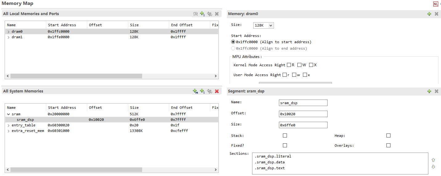
DSP can use sram_dsp, entry_table, and extra_reset_mem as system memory, and DRAM0/1 as local data memory. The Reset vector is stored in entry_table. DRAM0/1 can only store data.
Call0 ABI: Code and data can be placed in both sram_dsp and extra_reset_mem.
Window ABI: Code can only be placed in extra_reset_mem, while data can be placed in both sram_dsp and extra_reset_mem.
Placing Code/Data in SRAM
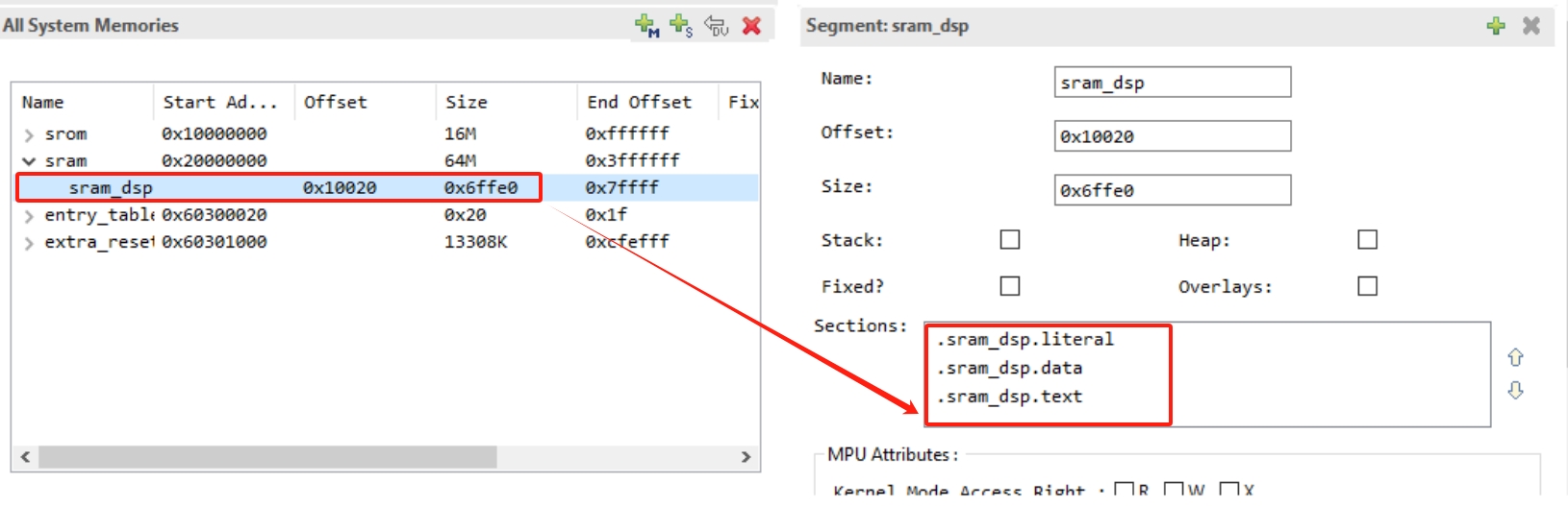
The bandwidth and latency of SRAM are significantly better than those of PSRAM. The default LSP (RTK_LSP) includes a segment named sram_dsp. Placing code or data in SRAM helps improve computation speed.
As shown in the figure below, RTK_LSP defines three segment memory regions in SRAM by default: .sram_dsp.text, .sram_dsp.data, and .sram_dsp.literal.
To place a single function in SRAM, declare and define it as follows:
extern void place_into_sram()__attribute__ ((section(".sram_dsp.text")));
void place_into_sram(){
       //detailed implentation
   }
To place data (such as an array) in SRAM, do this:
__attribute__ ((section(".sram_dsp.data"))) int array_in_psram[100];
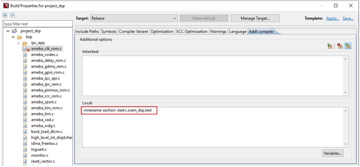
To place all functions in a source file (such as
ameba_clk_rom.c) in SRAM:Right-click the file and select
Build Properties, then set the relevant options to No in the pop-up window.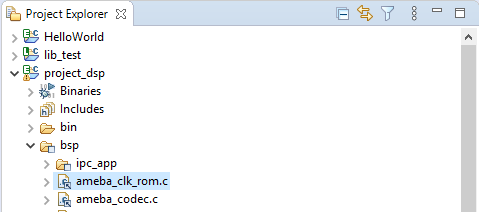
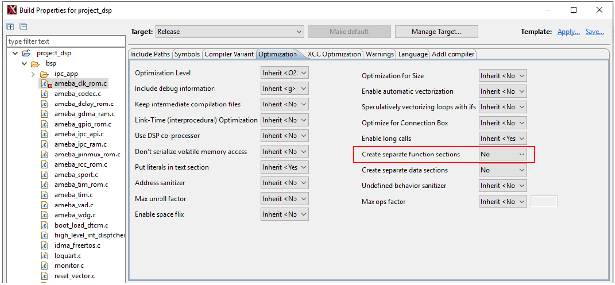
Then switch to the Addl compiler tab and add custom compilation parameters as shown below:
Modifying LSP Default Layout
MCU and DSP share PSRAM and SRAM, while DTCM is exclusively used by DSP. When the MCU’s PSRAM layout changes, the DSP’s LSP must be modified accordingly. Typically, DTCM and SRAM addresses remain at their defaults, with only PSRAM start and end addresses requiring adjustment. The PSRAM address adjustment method is as follows:
Navigate to the directory
{SDK}/project/img_utilitycd {SDK}/project/img_utility
Run
python lsp_modify.pyto view the current DSP PSRAM address:>> python lsp_modify.py Current LSP psram: Start Address: 0x60300000, End Address: 0x61000000, Size: 0xd00000 Invalid input. Please enter the start and end addresses in hex. Example: "python lsp_modify.py 0x60300000 0x61000000" DSP link script change FAIL.
Run
python lsp_modify.py <start psram address in hex> <end psram address in hex>to directly generate a new LSP and output the new LSP information:>> python lsp_modify.py 0x60400000 0x60A00000 Current LSP psram: Start Address: 0x60300000, End Address: 0x61000000, Size: 0xd00000 New LSP psram: Start Address: 0x60400000, End Address: 0x60a00000, Size: 0x600000 Warning : 'entry_table' start address not aligned to MPU min alignment (is 0x60400020, min alignment is 0x00001000) Warning : MPU region size smaller than min region size (0x60400020 - 0x60400040, is 32 must be at least 4096 bytes) Warning : 'unused' start address not aligned to MPU min alignment (is 0x60400040, min alignment is 0x00001000) New linker scripts generated in ../../project/RTK_LSP/RI-2021.8/HIFI5_PROD_1123_asic_UPG/RTK_LSP/ldscripts Change MCU layout (ameba_layout.ld) PSRAM_DSP_START to 0x60400000
This example adjusts the PSRAM start and end addresses to
0x60400000/0x60A00000. Since the script automatically generates the MPU table, the above address alignment warnings can be ignored and have no actual impact.Add the KEEP keyword in the linker script
RTK_LSP/ldscripts/elf32xtensa.x:.ipc_table : ALIGN(4) { _ipc_table_start = ABSOLUTE(.); KEEP(*(.ipc_table)) . = ALIGN (4); _ipc_table_end = ABSOLUTE(.); } >psram0_seg :psram0_phdr .command : ALIGN(4) { _command_start = ABSOLUTE(.); KEEP(*(.command)) . = ALIGN (4); _command_end = ABSOLUTE(.); } >psram0_seg :psram0_phdr
Modify the MCU memory layout file (
{MCU_SDK}/component/soc/amebalite/project/ameba_layout.ld) based on the above script output:#define PSRAM_DSP_START (0x60400000)Rebuild the DSP and MCU projects.
Note
Before using the script, ensure that the Xtensa toolchain’s bin directory has been added to the system/user PATH, otherwise executable files cannot be found.
If you have previously modified other MPU properties, please make the same modifications to the newly generated
mpu_table.c.Ensure that the newly generated
mpu_table.chas been added to the compilation project.