Power Consumption Measurement
This section, based on the default SDK, provides two low-power consumption examples—WiFi Wakeup and GPIO Wakeup—to help users quickly get familiar with and validate the low-power solution.
GPIO Wakeup Test
Test Environment and Tools Preparation
Hardware: The target development board, USB Type-C cable, testing computer, and Dupont wires (for connecting test pins and VCC/GND)
Serial debugging tool: Used to observe the running status of the board and to send test commands
Measuring equipment: Current source (or voltage source) or digital multimeter, and the corresponding host software
Test Code
The following is the test code using PA3 as the wakeup source. Add it to project_km4tz/src/main.c or project_km4/src/main.c, and call the test function near the end of the main function:
void gpio_irq_handler(void *id, u32 event)
{
        UNUSED(id);

        u32 GPIO_Pin = (event >> 16);
        u8 port_num = PORT_NUM(GPIO_Pin);
        GPIO_TypeDef *GPIO = (GPIO_TypeDef *)(GPIO_REG_BASE + port_num * 0x400);

        /* 0:AP; 1:NP */
        RTK_LOGI(TAG, "Core %d GPIO_IRQ_HANDLED %x!\n", SYS_CPUID(), GPIO_Pin);

        RTK_LOGI(TAG, "GPIO_INT_STATUS = 0x%x\n", GPIO->GPIO_INT_STATUS);

        GPIO_INTConfig(GPIO_Pin, DISABLE);

}
void gpio_test(void)
{
        GPIO_InitTypeDef GPIO_InitStruct = {
                .GPIO_Pin = _PA_3,
                .GPIO_PuPd = GPIO_PuPd_UP,
                .GPIO_Mode = GPIO_Mode_INT,
                .GPIO_ITTrigger = GPIO_INT_Trigger_EDGE,
                .GPIO_ITPolarity = GPIO_INT_POLARITY_ACTIVE_LOW,
        };
        GPIO_INTConfig(_PA_3, DISABLE);
        GPIO_Init(&GPIO_InitStruct);
        InterruptRegister(GPIO_INTHandler, GPIOA_IRQ, (u32)GPIOA_BASE, 3);
        InterruptEn(GPIOA_IRQ, 3);
        GPIO_UserRegIrq(_PA_3, gpio_irq_handler, &GPIO_InitStruct);
        SOCPS_SetAPWakeEvent(WAKE_SRC_GPIOA, ENABLE);
        GPIO_INTConfig(_PA_3, ENABLE);
}
Test Procedure
The following testing procedure is based on the official development board:
Refer to the schematic and remove the 0-ohm resistor between VDD33 and VDD33_S pins on the development board;
Connect the positive of a voltage source (must output 3.3V) to the VDD33_S pin, and the negative to the GND pin. Then open the voltage source’s host software and set the source output to 3.3V;
Connect the development board and PC using a USB Type-C cable;
Configure the GPIO test code;
Compile and download the firmware with GPIO wakeup configuration to the target board;
Open the serial debug software, select the COM port of the development board, and press chip en briefly;
Open the voltage source host software and view the current waveform;
After log output is finished, enter the test command
AT+TICKPS=Rto enter sleep mode, and observe the current waveform on the voltage source software at this moment.Then, connect one end of a Dupont wire to PA3 and briefly touch the other end to GND to wake up the CPU. The serial port will print out interrupt logs and you can also observe the current value change on the voltage source host software.
Note
If you are using a digital multimeter, set it to current mode, connect the positive lead to VDD33 and the negative lead to VDD33_S.
The LOG is shown in Wakeup from sleep by GPIO. After entering the command AT+TICKPS=R, the CPU enters sleep; after detecting the falling edge of GPIO, the CPU is woken up to execute the interrupt handler, and then goes back to sleep.
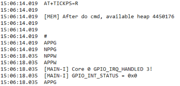
LOG when waking up from sleep by GPIO
The resulting current waveform is shown in Wakeup from sleep by GPIO. The average sleep current is 428.3uA, and the peak wakeup current is over 20mA.
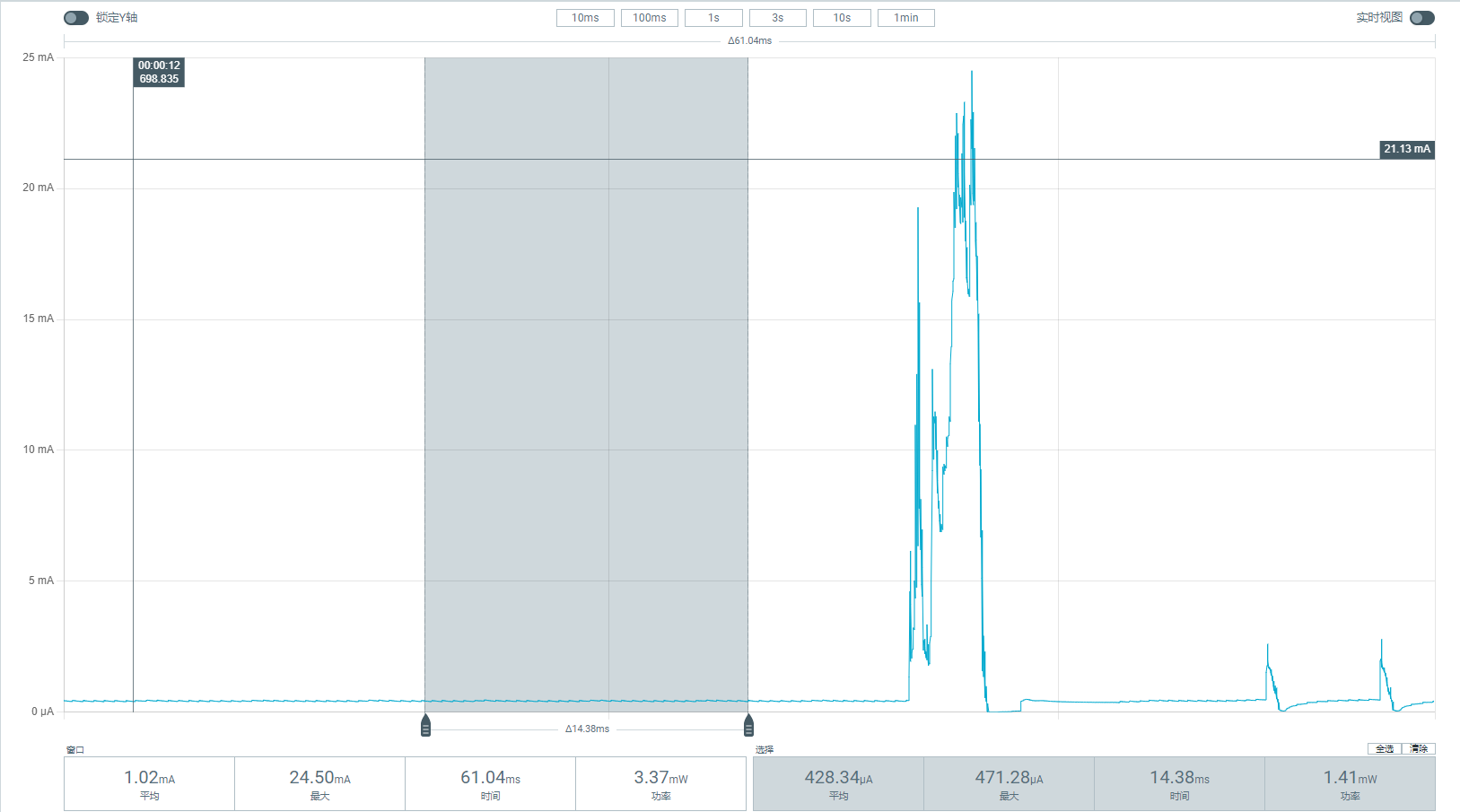
Wakeup from sleep by GPIO
WiFi Wakeup Test
Test Environment and Tools Preparation
Hardware: The target development board, USB Type-C cable, testing computer
Serial debugging tool: Used to observe the running status of the board and to send test commands
Measuring equipment: Current source (or voltage source) and the corresponding host software; a digital multimeter can also be used.
Test Procedure
In the amebaxxx_project directory, input
./menuconfig.pyto open the menu and enable WiFi optionsConnect the positive terminal of a voltage source (must output 3.3V) to the VDD33_S pin, and the negative to the GND pin. Then open the voltage source host software and set the source output to 3.3V;
Connect the development board and PC using a USB Type-C cable;
Compile and download the firmware with WiFi functionality to the target board;
Open the serial debug software, select the COM port of the development board, and briefly press chip en;
Open the voltage source host software and view the current waveform;
After log output is finished, enter the command
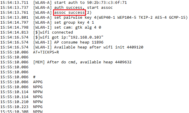
AT+WLCONN=ssid,<WiFi ssid>,pw,<password>to connect to WiFi, where WiFi ssid and password should be replaced with the available WiFi and its password (do not include the angle brackets).If connection is successful, “assoc success” will be printed in the serial terminal; then enter
AT+TICKPS=Rto observe the current waveform. If the connection fails, check if the hotspot exists and whether the antenna is properly connected on the dev board.
The LOG is shown in Periodic wakeups from Beacon sending/receiving. After entering the command AT+TICKPS=R, the CPU enters sleep, and wakes up approximately every 102ms to handle Beacon, before going back to sleep.
Periodic wakeups from Beacon sending/receiving
The current waveform of periodic WiFi wakeups in sleep mode is shown in Periodic wakeups from Beacon sending/receiving. On the left, the average current is over 20mA, where the CPU is still active. On the right, the average sleep current is 178.5uA, and during beacon sending/receiving, the current approaches 20mA.
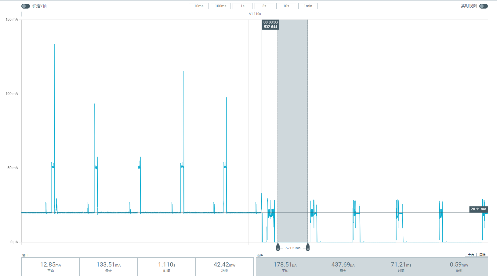
Periodic wakeups from Beacon sending/receiving