Feature
Full compliance with SDIO card specification version 2.0.
Support SDIO clock up to 25/50MHz
Support 4 bits I/O mode.
Dedicated DMA engine for data transfer to reduce CPU loading.
Architecture
The following figure shows the hardware architecture of SDIO Device interface. For power saving consideration, this hardware architecture is designed to be composed by 2 parts: On Domain and Off Domain. The On Domain is the part which is always powered on; the Off Domain will be turned off when chip is in the sleep mode. The On Domain implements the interface bus protocol and mainly is controlled by the host side. The Off Domain mainly is controlled by CPU, which implement the data packets DMA transfer.
The host side can access the SDIO control registers (also called SDIO local register) via SDIO command CMD52 or CMD53. The data packets are transferred via SDIO command CMD53.
For a SDIO packet transmit, the SDIO host need to read the available receive buffer count register to make sure SDIO device has memory space to receive this packet. Then the SDIO host sends a CMD53 with this packet to SDIO device. This packet data will be written to the Data FIFO first and then the TX DMA hardware will move these data from the Data FIFO to the given memory buffer. The DMA destination buffer is configured by the SDIO device driver.
For a SDIO packet receiving, the SDIO host will start a CMD53 transfer. RX DMA will continuously move data from the given memory buffer to the Data FIFO. The Data State Machine will read data from the Data FIFO and shift them to the SDIO bus.
Note
SDIO control register is different with SPDIO control register. Host can read/write all SDIO control registers and read some of SPDIO control registers. Ameba CPU can only read/write SPDIO Control registers.

Functional Description
SDIO Device Interface Control
The SDIO host side driver can control the SDIO Device hardware via SDIO control registers reading/writing. SPDIO device status also can be got by the SPDIO control registers reading. For packets transmission, the host can use CMD53 with a specific register address to read or write the SDPIO data FIFO.
Here is the “Register Address” coding of SDIO command CMD52 or CMD53 for control register read/write or data FIFO read/write:
Description |
Device ID (Bit [16]) |
Domain ID (Bit[15:13]) |
Address/Length (bit[12:0]) |
|---|---|---|---|
Control Register |
0 |
000b |
SDIO control register address or SPDIO control register address. |
TX FIFO |
0 |
100b |
TX packet length. The SDIO device hardware will check this length to see if the SPDIO device has enough of memory for this packet. If not, this command will be considered as an error command. The packet length includes the TX descriptor length, offset length and the packet payload length. The unit is 4-bytes. |
RX FIFO |
0 |
111b |
Stuff bits (No used, shall be set to 0) |
Note
SDIO device can response card recognition process command (such as CMD5, CMD3, CMD7) automatically. If host driver is compliant with standard protocol, it can be recognized to a high speed SDIO card. Then host can use CMD52/CMD53 to access SDIO/SGPIO control register and TX/RX FIFO by address as described above
DMA Transfer
The SDIO Device interface provides a high data rate interface for mass of data transmission. It has dedicated Tx/Rx DMA to transfer data between data FIFO and RAM.
Tx Flow
TX means the data transmission path is from the host side to SDIO device. The data from the host will be written into the SPDIO’s data FIFO first. Then the TX DMA hardware moves those data from data FIFO to the given buffer.
TX DMA Configuration
The memory addresses of buffers for storing TX packets data are described by TXBDs (TXBuffer Descriptor). A TXBD actually is 4-bytes memory which is located at RAM and containing the destination address of a TX DMA transfer for a TX packet data copying. The SDIO device driver is responsible for the TX DMA configuration and the TXBDs initialization.
The following figure is used to illustrate the TX DMA configuration. The SPDIO TX DMA configuration includes:
Register SPDIO_TXBD_ADDR is used to give the start address of TXBDs. The TX DMA will fetch TXBDs with an offset from this address. This address must be an 8 bytes aligned address.
Register SPDIO_TXBD_NUM is used to assign the number of total TXBDs.
Register TX_BUFF_UNIT_SIZE describes the size of the buffer for TX DMA. The unit is 64bytes. Ex. TX_BUFF_UNIT_SIZE register value is 24 means the size of the TX DMA buffer is 24 x 64 = 1536 bytes.
Each TXBD point to a TX DMA buffer. The start address of a TX DMA buffer must be an 8 bytes aligned address.
Register SPDIO_TXBD_WPTR is the index of the TXBD which point to the TX buffer for the next TX packet DMA transfer. This register is maintained by the SPDIO TX DMA hardware state machine. It will be updated as next available TXBD index whenever a TX packet DMA transfers is done. The difference of SPDIO_TXBD_WPTR between SPDIO_TXBD_RPTR is the number of free TX buffer. Once the number of free TX buffer is smaller than 1, the TX DMA hardware will stop working. Until the free TX buffer number is bigger or equal to 1.
Register SPDIO_TXBD_RPTR is maintained by the SPDIO Device driver. When processing a TX buffer for a TX DMA transfer is complete, the SPDIO device driver can either modify the corresponding TXBD to make it point to a new TX buffer or reuse the same TX buffer. The SPDIO Device driver need to update this register once the TX packets buffer processing is done. The SPDIO device driver should never let the SPDIO_TXBD_RPTR value run over the SPDIO_TXBD_WPTR value, otherwise some of TX packets will be dropped due to this error.

Tx DMA Behavior
On the event of SPDIO receives packet from host:
If the available TXBD Number (FREE_TXBD_NUM, which is calculated from SPDIO_TXBD_RPTR and SPDIO_TXBD_WPTR) is bigger than or equal to the packet number received from SDIO host, go to step2, else trigger TXBD_OVF interrupt.
If the Packet Size is larger than the TX Buffer Size assigned in register TX_BUFF_UNIT_SIZE, trigger TXPKT_SIZE_OVER_BUFF, else go to next step.
Put the packet to the TX Buffer which is described by the TXBD at index SPDIO_TXBD_WPTR.
Update SPDIO_TXBD_WPTR and update FREE_TXBD_NUM, which should be updated as long as SPDIO_TXBD_RPTR or SPDIO_TXBD_WPTR changes.
Trigger H2C_DMA_OK_INT interrupt to Ameba CPU to let the SPDIO driver to process received TX packets.
On the event of Ameba CPU receives H2C_DMA_OK_INT:
If SPDIO_TXBD_RPTR equals to SPDIO_TXBD_WPTR (All Packets have been processed by the SPDIO driver), clear H2C_DMA_OK_INT and return; else go to next step.
SPDIO driver processes the packet and informs application to move the packet.
SPDIO driver updates SPDIO_TXBD_RPTR after the packet processing is finished, go to step1.
Rx Flow
RX means the data transmission path is from Ameba to the host side. The RX DMA state machine hardware will copy data packets from the buffer on Ameba platform to the SPDIO’s data FIFO sequentially first, then the SPDIO hardware moves those data from data FIFO
to either SDIO Device IP shifter or the SPI Slave IP RX state machine shifter.
Rx DMA Configuration
A RXBD (RX Buffer Descriptor) is used to describe the start memory address of a RX packet data and its size. All of RXBDs should be located in a continuous memory block. The SPDIO device driver is responsible for the RX DMA configuration and the RXBDs initialization. A RX
packet can be described by multiple RXBDs. The RXBD format is shown as the following figure. And each field is described a s the following table:
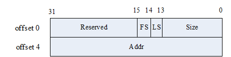
Offset(bit) |
Field |
Description |
|---|---|---|
0x0[13:0] |
Size |
The data size of the RX packet, in byte. This value is valid only when FS bit is 1. |
0x0[14] |
LS |
If the value of this field is 1, it means this RXBD is the last RXBD of a RX packet. |
0x0[15] |
FS |
If the value of this field is 1, it means this RXBD is the first RXBD of a RX packet. The Size field is valid only when this bit value is 1. |
0x4[31:0] |
Addr |
The start address of the RX packet data, it must be an 4-bytes aligned address. |
The following figure shows the illustration of the RX DMA configuration. The SPDIO RX DMA configuration includes:
Register SPDIO_RXBD_ADDR is used to give the start address of the memory for all RXBDs. The RX DMA will fetch RX_BDs with an offset from this address. This address must be an 8-bytes aligned address to make the RX DMA can work correctly.
Register SPDIO_RXBD_NUM is used to assign the number of total RXBDs.
Register SPDIO_RXBD_WPTR is maintained by the SPDIO Device driver. When the SPDIO driver sending a RX packet, the SPDIO driver fill one or more of RXBD to describe this RX packet. And then update the SPDIO_RXBD_WPTR by increase its value or wrapped as 0 to make its value is the index of the last RXBD of this sending RX packet. The SPDIO device driver should never let the SPDIO_RXBD_WPTR value run over the SPDIO_RXBD_RPTR value. Otherwise some of RX packets will be dropped due to this error.
Register SPDIO_RXBD_RPTR is the index of the RXBD which describing the RX packet for the RX DMA is going to transfer it to the host side. It is maintained by the SPDIO RX DMA hardware. Once a RX DMA transfer of a RX packet is finished, the RX DMA hardware will update this register to make its value is the index of the last fetched RXBD.

Rx DMA behavior
On the event of SPDIO Driver is request to send a packet to the host:
SPDIO Driver processes this packet and update SPDIO_RXBD_WPTR.
Set HCI_RX_REQ to trigger SPDIO RX DMA start the fetching of RXBD.
On the event of SPDIO RX DMA receives HCI_RX_REQ:
Update RX_REQ_LEN and RX_REQ_ADDR as described in the RXBD at index SPDIO_RXBD_RPTR.
Trigger an interrupt to host to make it start the RX packet transfer.
Get packet data from RX_FIFO and sends them to host.
SPDIO RX DMA updates the SPDIO_RXBD_RPTR when a packet transfer is finished.
If SPDIO_RXBD_RPTR < SPDIO_RXBD_WPTR, go to step1; else go to next step.
Clear HCI_RX_REQ.
Trigger C2H_DMA_OK_INT interrupt to inform the SPDIO driver that RX packets has been transferred.
On the event of the Ameba CPU receive s C2H_DMA_OK_INT interrupt:
Inform the SPDIO driver that RX packets have been transferred and one or more RXBD is free.
Register
Offset of SPDIO control register for Ameba CPU access is 0x100 less than it for host access. For example, offset of SDIO_REG_RXBD_NUM is 0x1B4 for host and 0xB4 for Ameba CPU.
In the “Access” column of SPDIO control register table, CPU means Ameba CPU and DRV means host driver.
SDIO Control Register
SDIO_STATIS_RECOVERY_TIMEOUT
Name: SDIO_STATIS_RECOVERY_TIMEOUT Register
Width: 16bit
Initial Value: 0x0C00
Offset: 0002h
Bit |
Access |
INI |
Symbol |
Description |
|---|---|---|---|---|
15:0 |
R/W |
SDIO_STATIS_RECOVERY_TIMEOUT |
It is SDIO status timeout. The unit is 32usec. The default value is 0xc00 means that timeout is 98304 usec ( 32*0xc00) |
SDIO_HIMR
Name: SDIO_HIMR Register
Width: 32bit
Initial Value: 0xF
Offset: 0014h
Bit |
Access |
INI |
Symbol |
Description |
|---|---|---|---|---|
31:23 |
R/W |
NO USED |
NO USED |
|
22 |
R/W |
CPU_NOT_RDY_MSK |
This bit is clear, and CPU_NOT_RDY is masked. |
|
21 |
R/W |
NO USED |
NO USED |
|
20 |
R/W |
H2C_BUS_FAIL_MSK |
This bit is clear, and H2C_BUS_FAIL_INT is masked |
|
19 |
R/W |
CPWM2_MSK |
This bit is clear, and CPWM2_INT is masked |
|
18 |
R/W |
CPWM1_MSK |
This bit is clear, and CPWM1_INT is masked |
|
17 |
R/W |
C2H_MSG_MSK |
This bit is clear, and C2H_MSG_INT is masked |
|
16:5 |
R/W |
NO USED |
NO USED |
|
4 |
R/W |
TXBD_OVERFLOW_MSK |
This bit is clear, and TXBD_OVERFLOW is masked |
|
3 |
R/W |
TXAGG_SIZE_MISMATCH_MSK |
This bit is clear, and TXAGG_SIZE_MISMATCH is masked |
|
2 |
R/W |
TXPKT_SIZE_OVER_BUFF_MSK |
This bit is clear, and TXPKT_SIZE_OVER_BUFF is masked |
|
1 |
R/W |
TXFIFO_AVAL_MSK |
This bit is clear, and TXFIFO_AVAL _INT INT is masked |
|
0 |
R/W |
RX_REQUEST_MSK |
This bit is clear, and RX_REQUEST_INT is masked. |
SDIO_HISR
Name: SDIO_HISR Register
Width: 32bit
Initial Value: 0x0
Offset: 0018h
Bit |
Access |
INI |
Symbol |
Description |
|---|---|---|---|---|
31:21 |
NO USED |
NO USED |
||
22 |
R/W1C |
CPU_NOT_RDY |
When host send CMD53 for to access SDIO OFF, and CPU_RDY_IND=0, trigger this interrupt |
|
21 |
NO USED |
NO USED |
||
20 |
R/W1C |
H2C_BUS_FAIL |
H2C BUS Fail Interrupt:To notify Host DMA transfer error by AHB BUS resource conflict. Host get this error INT, and know the previous packet fail, and need to re-send or IO_RESET device! |
|
19 |
R/W1C |
CPWM2_INT |
CPWM2 Write Interrupt: This interrupt will be raised when FW writes CPWM2_TOGGLING of CPWM2 register. Write 1 clear |
|
18 |
R/W1C |
CPWM1_INT |
CPWM1 Write Interrupt: This interrupt will be raised when FW writes CPWM1_TOGGLING of CPWM1 register. Write 1 clear |
|
17 |
R/W1C |
C2H_MSG_INIT |
CPU to Host Message INT Status: This interrupt will be raised when FW sends a C2H MSG Write 1 clear |
|
16:5 |
NO USED |
NO USED |
||
4 |
R/W1C |
TXBD_OVF |
When host send TX packet and there is no enough TXBD, trigger this interrupt |
|
3 |
R/W1C |
TX_AGG_SIZE_MISMATCH |
If the total size of the tx aggregation packets is LARGER the CMD53 Data Size, this interrupt trigger |
|
2 |
R/W1C |
TXPKT_SIZE_OVER_BUFF |
If the Packet size (Aggregated or not) is larger than the Buffersize assigned in the TX_BD, this interrupt trigger |
|
1 |
R |
TXAVAL_INT |
When the free page is lower than SDIO_AVAI_BD_NUM_TH_L and higher than SDIO_AVAI_BD_NUM_TH_H consequently, this interrupt occurs. When Host read FREE_TXBD_NUM, the bit becomes zero. When using CMD52 to read FREE_TXBD_NUM, we suggest to read offset 0x23->0x22->0x21->0x20 consequently |
|
0 |
R |
RX_REQUEST |
This bit is set when one complete RX aggregation packet is received into RXPKTBUF and RX_REQUEST_MSK is set to 1. Only when RX FIFO is empty, the bit becomes zero. |
RX0_REQ_LEN
Name: RX0_REQ_LEN Register
Width: 32bit
Initial Value: 0x0
Offset 001Ch
Bit |
Access |
INI |
Symbol |
Description |
|---|---|---|---|---|
31 |
R |
RX_REQ_LEN_RDY |
Indicate RX0_REQ_LEN is ready |
|
30:24 |
RSVD |
|||
23:0 |
R |
RX0_REQ_LEN |
The requested RX Packet length; Unit: Byte For the RX Aggregation case, the length is total length of the packet. Each packet is 8byte 4byte alignment. This value is legal only when RX_REQ_LEN_RDY is 1 |
FREE_TXBD_NUM
Name: FREE_TXBD_NUM Register
Width: 16bit
Initial Value: 0x0
Offset 0020h
Bit |
Access |
INI |
Symbol |
Description |
|---|---|---|---|---|
15:0 |
R |
FREE_TXBD_NUM |
The free TXBD Number. |
HCPWM
Name: HCPWM Register
Width: 8bit
Initial Value: 0x0
Offset 0038h
Bit |
Access |
INI |
Symbol |
Description |
|---|---|---|---|---|
7 |
R |
TOGGLING |
Toggling Bit: this is the one bit sequence number field. Interrupt is issued when this bit is changed from “ to “ or from “ to “. |
|
6:0 |
R |
RSVD |
RSVD |
HCPWM2
Name: HCPWM2 Register
Width: 16bit
Initial Value: 0x0
Offset 003Ah
Bit |
Access |
INI |
Symbol |
Description |
|---|---|---|---|---|
15 |
R |
TOGGLING |
Toggling Bit: this is the one bit sequence number field. Interrupt is issued when this bit is changed from “ to “ or from “ to “. |
|
14:0 |
R |
RSVD |
RSVD |
REG_SDIO_H2C_MSG
Name: REG_SDIO_H2C_MSG Register
Width: 32bit
Initial Value: 0x0
Offset 0060h
Bit |
Access |
INI |
Symbol |
Description |
|---|---|---|---|---|
31 |
R/W |
TOGGLING |
Toggling Bit: this is the one bit sequence number field. Interrupt is issued when this bit is changed from “ to “ or from “ to “. |
|
30:0 |
R/W |
REG_SDIO_H_MSG |
Driver to FW Message |
REG_SDIO_C2H_MSG
Name: REG_SDIO_C2H_MSG Register
Width: 32bit
Initial Value: 0x0
Offset 0064h
Bit |
Access |
INI |
Symbol |
Description |
|---|---|---|---|---|
31 |
R |
TOGGLING |
Toggling Bit: this is the one bit sequence number field. Interrupt is issued when this bit is changed from “ to “ or from “ to “. |
|
30:0 |
R |
REG_SDIO_C2H_MSG |
FW to Driver Message |
REG_SDIO_H2C_MSG_EXT
Name: REG_SDIO_H2C_MSG_EXT Register
Width: 32bit
Initial Value: 0x0
Offset 0068h
Bit |
Access |
INI |
Symbol |
Description |
|---|---|---|---|---|
31:0 |
R/W |
REG_SDIO_H_MSG_EXT |
Driver to FW EXT Message, trigger by 0x0060[31] |
REG_SDIO_C2H_MSG_EXT
Name: REG_SDIO_C2H_MSG_EXT Register
Width: 32bit
Initial Value: 0x0
Offset 006Ch
Bit |
Access |
INI |
Symbol |
Description |
|---|---|---|---|---|
31:0 |
R |
REG_SDIO_C2H_MSG_EXT |
FW to Driver EXT Message |
HRPWM
Name: HRPWM Register
Width: 8bit
Initial Value: 0x7
Offset 0080h
Bit |
Access |
INI |
Symbol |
Description |
|---|---|---|---|---|
7 |
R/W |
TOGGLING |
Toggling Bit: this is the one bit sequence number field. Interrupt is issued when this bit is changed from “ to “ or from “ to “. |
|
6:0 |
R/W |
RSVD |
RSVD |
HRPWM2
Name: HRPWM2 Register
Width: 16bit
Initial Value: 0x0
Offset 0082h
Bit |
Access |
INI |
Symbol |
Description |
|---|---|---|---|---|
15 |
R/W |
TOGGLING |
Toggling Bit: this is the one bit sequence number field. Interrupt is issued when this bit is changed from “ to “ or from “ to “. |
|
14:0 |
R/W |
RSVD |
RSVD |
CPU_INDICATION
Name: CPU_INDICATION Register
Width: 8bit
Initial Value:
Offset 0087h
Bit |
Access |
INI |
Symbol |
Description |
|---|---|---|---|---|
7:4 |
R/W |
SDIO_TEST_BUSY_CNT |
For Device test BUSY control count, BUSY time ~= BUSY_CNT * 16-SD_CLK |
|
3:1 |
RSVD |
|||
0 |
R |
CPU_RDY_IND |
Used to indicate that CPU is ready for TRX. Default: 0 This bit is synchronized from SYTEM_CPU_RDY_IND(Offset 0x1C5) |
ERR_FLAG
Name: ERR_FLAG Register
Width: 8bit
Initial Value: 0x0
Offset 00C0h
Bit |
Access |
INI |
Symbol |
Description |
|---|---|---|---|---|
7:0 |
R/W1C |
ERR_FLAG |
ERR FLAG for SDIO DEBUG |
SDIO_CMD_ERRCNT
Name: SDIO_CMD_ERRCNT Register
Width: 8bit
Initial Value: 0x0
Offset 00C2h
Bit |
Access |
INI |
Symbol |
Description |
|---|---|---|---|---|
7:0 |
R/W |
CMD_CRC_ERR_CNT |
The number of CRC error of SDIO Command |
SDIO_DATA_ERRCNT
Name: SDIO_DATA_ERRCNT Register
Width: 8bit
Initial Value: 0x0
Offset 00C3h
Bit |
Access |
INI |
Symbol |
Description |
|---|---|---|---|---|
7:0 |
R/W |
DATA_CRC_ERR_CNT |
The number of CRC error of SDIO Data Block |
SDIO_CRC_ERR_INDEX
Name: SDIO_CRC_ERR_INDEX Register
Width: 8bit
Initial Value: 0x0
Offset 00C4h
Bit |
Access |
INI |
Symbol |
Description |
|---|---|---|---|---|
7:5 |
RSVD |
|||
4 |
R/W1C |
D3_CRC_ERR |
Indicate there is crc error on SD_D3 It is suggested to clear it by CMD52 |
|
3 |
R/W1C |
D2_CRC_ERR |
Indicate there is crc error on SD_D2 It is suggested to clear it by CMD52 |
|
2 |
R/W1C |
D1_CRC_ERR |
Indicate there is crc error on SD_D1 It is suggested to clear it by CMD52 |
|
1 |
R/W1C |
D0_CRC_ERR |
Indicate there is crc error on SD_D0 It is suggested to clear it by CMD52 |
|
0 |
RSVD |
SDIO_AVAI_BD_NUM_TH_L
Name: SDIO_AVAI_BD_NUM_TH_L Register
Width: 32bit
Initial Value: 0x0
Offset 00D0h
Bit |
Access |
INI |
Symbol |
Description |
|---|---|---|---|---|
31:16 |
RSVD |
|||
15:0 |
R/W |
SDIO_AVAI_BD_NUM_TH_L |
Low threshold for TXBD Number |
SDIO_AVAI_BD_NUM_TH_H
Name: SDIO_AVAI_BD_NUM_TH_H Register
Width: 32bit
Initial Value: 0x0
Offset 00D4h
Bit |
Access |
INI |
Symbol |
Description |
|---|---|---|---|---|
31:16 |
RSVD |
|||
15:0 |
R/W |
SDIO_AVAI_BD_NUM_TH_H |
High threshold for TXBD Number |
SDIO_RX_AGG_CFG
Name: SDIO_RX_AGG_CFG Register
Width: 16bit
Initial Value: 0x0
Offset 00D8h
Bit |
Access |
INI |
Symbol |
Description |
|---|---|---|---|---|
15 |
R/W |
SDIO_RX_AGG_EN |
Enable SDIO Bus RX Aggregation |
|
14:8 |
R/W |
RX_AGG_TO |
Timeout threshold for RX Agg; Unit: 32us |
|
7:0 |
R/W |
RX_AGG_BD_COUNT_TH |
RX_BD count threshold for RX Agg |
SDIO_CMD_TIMING_CTRL
Name: SDIO_CMD_TIMING_CTRL Register
Width: 8bit
Initial Value: 0x0
Offset 00DCh
Bit |
Access |
INI |
Symbol |
Description |
|---|---|---|---|---|
7:4 |
R/W |
SD_CMD_DLY_SEL |
Used to control the delay of SD_CMD |
|
3:0 |
RSVD |
SD_DATA01_TIMING_CTRL
Name: SD_DATA01_TIMING_CTRL Register
Width: 8bit
Initial Value: 0x0
Offset 00DDh
Bit |
Access |
INI |
Symbol |
Description |
|---|---|---|---|---|
7:4 |
R/W |
SD_DATA1_DLY_SEL |
Used to control the delay of SD_DATA1 |
|
3:0 |
R/W |
SD_DATA0_DLY_SEL |
Used to control the delay of SD_DATA0 |
SD_DATA23_TIMING_CTRL
Name: SD_DATA23_TIMING_CTRL Register
Width: 8bit
Initial Value: 0x0
Offset 00DEh
Bit |
Access |
INI |
Symbol |
Description |
|---|---|---|---|---|
7:4 |
R/W |
SD_DATA3_DLY_SEL |
Used to control the delay of SD_DATA3 |
|
3:0 |
R/W |
SD_DATA2_DLY_SEL |
Used to control the delay of SD_DATA2 |
SPDIO Control Registers
SPDIO_TXBD_ADDR
Name: SPDIO_TXBD_ADDR Register
Width: 32bit
Initial Value: 0x0
Offset: 01A0h
Bit |
Access |
INI |
Symbol |
Description |
|---|---|---|---|---|
31:0 |
CPU: R/W DRV: R |
SPDIO_TXFIFO_ADDR |
The base address of TXBD The value of this register should be configure by CPU It should be 4 byte alignment (Because TXBD Size is 8 Byte). |
SPDIO_TXBD_NUM
Name: SPDIO_TXBD_NUM Register
Width: 16bit
Initial Value: 0x0
Offset: 01A4h
Bit |
Access |
INI |
Symbol |
Description |
|---|---|---|---|---|
15:0 |
CPU: R/W DRV: R |
SPDIO_TXBD_NUM |
The Number of TXBD. Unit: Number The value of this register should be configured by CPU |
SPDIO_TXBD_WPTR
Name: SPDIO_TXBD_WPTR Register
Width: 16bit
Initial Value: 0x0
Offset: 01A8h
Bit |
Access |
INI |
Symbol |
Description |
|---|---|---|---|---|
[31] |
R |
SPDIO_TXBD_H2C_WPTR_WRAP |
Toggle once wptr reaches txbd_size |
|
15:0 |
R |
SPDIO_TXBD_H_WPTR |
When the packet has been sent from Host to TX Buffer, this index should be updated by SDIO IP. |
SPDIO_TXBD_RPTR
Name: SPDIO_TXBD_RPTR Register
Width: 16bit
Initial Value: 0x0
Offset: 01ACh
Bit |
Access |
INI |
Symbol |
Description |
|---|---|---|---|---|
[31] |
CPU: RW DRV: R |
SPDIO_TXBD_H2C_RPTR_WRAP |
Software should write(toggle) this bit once rptr reaches txbd_size |
|
15:0 |
CPU: RW DRV: R |
SPDIO_TXBD_H_RPTR |
When the packet has been processed by CPU and moved to MAC TX FIFO, this index should be updated by CPU. |
SPDIO_RXBD_ADDR
Name: SPDIO_RXBD_ADDR Register
Width: 32bit
Initial Value: 0x0
Offset: 01B0h
Bit |
Access |
INI |
Symbol |
Description |
|---|---|---|---|---|
31:0 |
CPU: RW DRV: R |
SPDIO_RXBD_ADDR |
The base address of RX BD. The value of this register should be configured by CPU. It should be 8-Byte alignment |
SPDIO_RXBD_NUM
Name: SPDIO_RXBD_NUM Register
Width: 16bit
Initial Value: 0x0100
Offset: 01B4h
Bit |
Access |
INI |
Symbol |
Description |
|---|---|---|---|---|
15:0 |
CPU: RW DRV: R |
SPDIO_RXBD_NUM |
The total count of RX BD The value of this register should be configured by CPU. The unit is BD count |
SPDIO_RXBD_C2H_WPTR
Name: SPDIO_RXBD_C2H_WPTR Register
Width: 16bit
Initial Value: 0x0
Offset: 01B6h
Bit |
Access |
INI |
Symbol |
Description |
|---|---|---|---|---|
15:0 |
CPU: RW DRV: R |
SPDIO_RXBD_C2H_WPTR |
When the packet has been processed by CPU and to be moved to host, this index should be updated by CPU |
SPDIO_RXBD_C2H_RPTR
Name: SPDIO_RXBD_C2H_RPTR Register
Width: 16bit
Initial Value: 0x0
Offset: 01B8h
Bit |
Access |
INI |
Symbol |
Description |
|---|---|---|---|---|
15:0 |
CPU: R DRV: R |
SPDIO_RXBD_C2H_RPTR |
When the packet has been moved to host, this index should be updated by SDIO IP. |
HCI_RX_REQ
Name: HCI_RX_REQ Register
Width: 8bit
Initial Value: 0x0
Offset: 01BAh
Bit |
Access |
INI |
Symbol |
Description |
|---|---|---|---|---|
7:1 |
||||
0 |
CPU: RW DRV: R |
HCI_RX_REQ |
CPU triggers this bit to enable SDIO IP RX transfer by fetch BD info. SDIO fetch BD to get the RX length and address and transfer RX packet to Host, and clear this bit when all BD transfer done. |
CPU_RST_SDIO_DMA
Name: CPU_RST_SDIO_DMA Register
Width: 8bit
Initial Value: 0x0
Offset: 01BBh
Bit |
Access |
INI |
Symbol |
Description |
|---|---|---|---|---|
7 |
CPU: RW DRV: R |
CPU_RST_SDIO_DMA |
CPU set this bit to reset SDIO DMA. This bit is auto clear. |
|
6:1 |
RSVD |
|||
0 |
CPU: RW DRV: R |
SDIO_DAT_EDGE_INV |
Invert SDIO Latch input data edge. |
SPDIO_RX_REQ_ADDR
Name: SPDIO_RX_REQ_ADDR Register
Width: 32bit
Initial Value: 0x0
Offset: 01BCh
Bit |
Access |
INI |
Symbol |
Description |
|---|---|---|---|---|
31:0 |
CPU: RW DRV: R |
SPDIO_RX_REQ_ADDR |
The address of the requested RX Packet. This is unnecessary for driver. |
SPDIO_CPU_INT_MASK
Name: SPDIO_CPU_INT_MASK Register
Width: 16bit
Initial Value: 0x0
Offset: 01C0h
Bit |
Access |
INI |
Symbol |
Description |
|---|---|---|---|---|
15:12 |
RSVD |
|||
11 |
CPU: RW DRV: R |
HOST_CMD11_INT_MSK |
This bit is clear, and HOST_CMD11_INT is masked |
|
10 |
CPU: RW DRV: R |
HOST_WAKE_CPU_INT_MSK |
This bit is clear, and HOST_WAKE_CPU_INT is masked |
|
9 |
CPU: RW DRV: R |
RX_BD_AVAI_INT_MSK |
This bit is clear, and RX_BD_AVAI_INT is masked |
|
8 |
CPU: RW DRV: R |
RX_BD_FLAG_ERR_INT_MSK |
This bit is clear, and RX_BD_FLAG_ERR_INT is masked |
|
7 |
CPU: RW DRV: R |
SDIO_RST_CMD_INT_MSK |
This bit is clear, and SDIO_RST_CMD_INT is masked |
|
6 |
CPU: RW DRV: R |
RPWM2_INT_MSK |
This bit is clear, and RPWM2_INT is masked |
|
5 |
CPU: RW DRV: R |
RPWM_INT_MSK |
This bit is clear, and RPWM_INT is masked |
|
4 |
CPU: RW DRV: R |
H_MSG_INT_MSK |
This bit is clear, and H_MSG_INT is masked |
|
3 |
CPU: RW DRV: R |
C2H_DMA_OK_MSK |
This bit is clear, and C2H_DMA_OK_INT is masked |
|
2 |
CPU: RW DRV: R |
H_DMA_OK_MSK |
This bit is clear, and H_DMA_OK_INT is masked |
|
1 |
CPU: RW DRV: R |
H_BUS_RES_FAIL_MSK |
This bit is clear, and H_BUS_RES_FAIL_INT is masked |
|
0 |
CPU: RW DRV: R |
TXBD_H_OVF _MSK |
This bit is clear, and TXBD_H_OVF is masked |
SPDIO_CPU_INT_REG
Name: SPDIO_CPU_INT_REG Register
Width: 16bit
Initial Value: 0x0
Offset: 01C2h
Bit |
Access |
INI |
Symbol |
Description |
|---|---|---|---|---|
15:12 |
RSVD |
|||
11 |
CPU: RW DRV: R |
HOST_CMD11_INT |
When Host sends CMD11 to notify that the signal voltage level is going to switch to 1.8v, the HW should issue this interrupt to notify the local CPU to do the LDO power voltage level switch. |
|
10 |
CPU: R/W DRV: R |
HOST_WAKE_CPU_INT |
When Host Send TRX CMD53 while CPU is not ready (SYSTEM_CPU_RDY_IND=0, or CPU_RDY_IND=0), trigger this interrupt to wake CPU, and then indicate BUSY status to host. CPU should be able to receive this interrupt even CPU clock is gated; therefore, this interrupt should be connected to System On circuit. |
|
9 |
CPU: R/W DRV: R |
RX_BD_AVAI_INT |
If the free RXBD Number become larger than FREE_RXBD_COUNT(0x1D8), trigger this interrupt. This interrupt trigger only once when free RXBD number cross FREE_RXBD_COUNT |
|
8 |
CPU: R/W DRV: R |
RX_BD_FLAG_ERR_INT |
Trigger by SDIO to CPU when detect RX_BD error |
|
7 |
CPU: R/W DRV: R |
SDIO_RST_CMD_INT |
Trigger by SDIO to CPU when SDIO is reset. CPU should be able to receive this interrupt even CPU clock is gated; therefore, this interrupt should be connected to System On circuit. |
|
6 |
CPU: R/W DRV: R |
RPWM2_INT |
Trigger by SDIO to CPU that RPWM2 occurs (HRPWM is toggled) CPU should be able to receive this interrupt even CPU clock is gated; therefore, this interrupt should be connected to System On circuit. |
|
5 |
CPU: R/W DRV: R |
RPWM1_INT |
Trigger by SDIO to CPU that RPWM1 occurs(HRPWM2 is written) CPU should be able to receive this interrupt even CPU clock is gated; therefore, this interrupt should be connected to System On circuit. |
|
4 |
CPU: R/W DRV: R |
H2C_MSG_INT |
Trigger by SDIO to CPU that H_MSG_INT occurs(REG_SDIO_H_MSG is written) |
|
3 |
CPU: R/W DRV: R |
C2H_DMA_OK |
Trigger by SDIO to CPU that packet is sent from RXFIFO to Host |
|
2 |
CPU: R/W DRV: R |
H2C_DMA_OK |
Trigger by SDIO to CPU that packet is sent from Host to TXFIFO |
|
1 |
CPU: R/W DRV: R |
H2C_BUS_RES_FAIL |
If SDIO is going to move packet to TX FIFO and fails to get bus resource, this interrupt raise. Driver Write 1 clear |
|
0 |
CPU: R/W DRV: R |
TXBD_H2C_OVF |
If there is not enough TX_BD for TX Packet, this bit raise. Driver Write 1 clear |
CCPWM
Name: CCPWM Register
Width: 8bit
Initial Value: 0x0
Offset: 01C4h
Bit |
Access |
INI |
Symbol |
Description |
|---|---|---|---|---|
7 |
CPU: R/W DRV: R |
TOGGLING |
Toggling Bit: this is the one bit sequence number field. Interrupt is issued when this bit is changed from “ to “ or from “ to “. |
|
6:4 |
CPU:R/W DRV: R |
NO USED |
NO USED |
SYS_CPU_INDICATION
Name: SYS_CPU_INDICATION Register
Width: 8bit
Initial Value: 0x0
Offset: 01C5h
Bit |
Access |
INI |
Symbol |
Description |
|---|---|---|---|---|
7:2 |
RSVD |
|||
1 |
R/W |
readee_done |
After cccr reg is configured, write this bit to 1 |
|
0 |
R/W |
SYSTEM_CPU_RDY_IND |
Used to indicate that CPU is ready for TRX. Default: 0 This bit is synchronized to CPU_RDY_IND(Offset: 0x87) |
CCPWM2
Name: CCPWM2 Register
Width: 16bit
Initial Value: 0x0
Offset: 01C6h
Bit |
Access |
INI |
Symbol |
Description |
|---|---|---|---|---|
15 |
CPU: R/W DRV: R |
TOGGLING |
Toggling Bit: this is the one bit sequence number field. Interrupt is issued when this bit is changed from “ to “ or from “ to “. |
|
14:0 |
CPU: R/W DRV: R |
NO USED |
NO USED |
REG_CPU_H2C_MSG
Name: REG_CPU_H2C_MSG Register
Width: 32bit
Initial Value: 0x0
Offset: 01C8h
Bit |
Access |
INI |
Symbol |
Description |
|---|---|---|---|---|
31 |
CPU: R DRV: R |
TOGGLING |
Toggling Bit: this is the one bit sequence number field. Interrupt is issued when this bit is changed from “ to “ or from “ to “. |
|
30:0 |
CPU: R DRV: R |
REG_CPU_H_MSG |
Driver to FW Message |
REG_CPU_C2H_MSG
Name: REG_CPU_C2H_MSG Register
Width: 32bit
Initial Value: 0x0
Offset: 01CCh
Bit |
Access |
INI |
Symbol |
Description |
|---|---|---|---|---|
31 |
CPU: R/W DRV: R |
TOGGLING |
Toggling Bit: this is the one bit sequence number field. Interrupt is issued when this bit is changed from “ to “ or from “ to “. |
|
30:0 |
CPU: R/W DRV: R |
REG_CPU_C2H_MSG |
FW to Driver Message |
CRPWM
Name: CRPWM Register
Width: 8bit
Initial Value: 0x7
Offset: 01D0h
Bit |
Access |
INI |
Symbol |
Description |
|---|---|---|---|---|
7 |
CPU: R DRV: R |
TOGGLING |
Toggling Bit: this is the one bit sequence number field. Interrupt is issued when this bit is changed from “ to “ or from “ to “. |
|
6:4 |
CPU: R DRV: R |
NO USED |
NO USED |
CRPWM2
Name: CRPWM2 Register
Width: 16bit
Initial Value: 0x0
Offset: 01D2h
Bit |
Access |
INI |
Symbol |
Description |
|---|---|---|---|---|
15 |
CPU: R DRV: R |
TOGGLING |
Toggling Bit: this is the one bit sequence number field. Interrupt is issued when this bit is changed from “ to “ or from “ to “. |
|
14:0 |
CPU: R DRV: R |
NO USED |
NO USED |
AHB_DMA_CTRL
Name: AHB_DMA_CTRL Register
Width: 32bit
Initial Value: 0x74004040
Offset: 01D4h
Bit |
Access |
INI |
Symbol |
Description |
|---|---|---|---|---|
31 |
CPU: RW DRV: R |
DISPATCH_TXAGG_PKT |
Enable SPDIO to dispatch the Aggregated TX packet. |
|
30:28 |
CPU: RW DRV: R |
AHB_BURST_TYPE |
This field is used to control to SPDIO AHB support Burst type. b100: Support Burst 16 DW b010: Support Burst 8 DW b001: Support Burst 4 DW Default is b111, all support. |
|
27:24 |
CPU: RW DRV: R |
RX_AHB_BUSY_WAIT_CNT |
When SPDIO RX transfer, AHB controller will wait BUSY counter for AHB access target not response READY signal. If timeout, AHB controller will issue AHB_BUS_RES_FAIL INT to CPU. |
|
23:22 |
CPU: R DRV: R |
AHBM_SPDIO_TRANS |
SPDIO AHB Master HTRANS signal |
|
21 |
CPU: R DRV: R |
AHBM_SPDIO_READY |
SPDIO AHB Master Hready signal |
|
20 |
CPU: R DRV: R |
NO USED |
NO USED |
|
19:16 |
CPU: R DRV: R |
AHB_DMA_CS |
AHB DMA state |
|
15 |
CPU: R DRV: R |
NO USED |
NO USED |
|
14:8 |
CPU: RW DRV: R |
SPDIO_RXFF_WLEVEL |
SPDIO FIFO RX water level Range 1~126, it can be modified only when AHB_DMA_CS = 000 |
|
7 |
CPU: R DRV: R |
NO USED |
NO USED |
|
6:0 |
CPU: RW DRV: R |
SPDIO_TXFF_WLEVEL |
SPDIO FIFO TX water level Range 1~126, it can be modified only when AHB_DMA_CS = 000 |
FREE_RXBD_COUNT
Name: FREE_RXBD_COUNT Register
Width: 32bit
Initial Value: 0x10100
Offset: 01D8h
Bit |
Access |
INI |
Symbol |
Description |
|---|---|---|---|---|
31:16 |
CPU: RW DRV: R |
FREE_RXBD_COUNT |
If SPDIO_RXBD_C2H_RPTR is updated and the free RXBD Number is larger than FREE_RXBD_COUNT, trigger RX_BD_AVAI_INT interrupt. |
|
15:8 |
CPU: RW DRV: R |
TX_BUFF_UNIT_SIZE |
The Size of each single TX Buffer which is addressed by TX_BD Unit: 64Byte Ex: 0x01=>64Byte 0x10=>1024Byte |
|
7 |
CPU: R DRV: R |
NO USED |
NO USED |
|
6:0 |
CPU: R DRV: R |
FIFO_CNT |
The SPDIO Local FIFO counter, for debug usage |
REG_CPU_H2C_MSG_EXT
Name: REG_CPU_H2C_MSG_EXT Register
Width: 32bit
Initial Value: 0x0
Offset: 01DCh
Bit |
Access |
INI |
Symbol |
Description |
|---|---|---|---|---|
31 |
R |
TOGGLING |
Toggling Bit: this is the one bit sequence number field. Interrupt is issued when this bit is changed from “ to “ or from “ to “. |
|
30:0 |
R |
REG_CPU_H_MSG_EXT |
Driver to FW Message |
REG_CPU_C2H_MSG_EXT
Name: REG_CPU_C2H_MSG_EXT Register
Width: 32bit
Initial Value: 0x0
Offset: 01E0h
Bit |
Access |
INI |
Symbol |
Description |
|---|---|---|---|---|
31 |
R/W |
TOGGLING |
Toggling Bit: this is the one bit sequence number field. Interrupt is issued when this bit is changed from “ to “ or from “ to “. |
|
30:0 |
R/W |
REG_CPU_C2H_MSG_EXT |
FW to driver Message |