Introduction
The pseudo I2C only has Tx function and does not require slave reply ACK and slave address confirmation functions.
Design Implementation
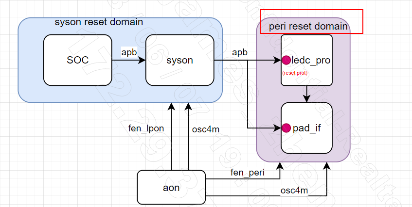
Reset Domain
Ledc_Pro and pad ctrl belong to the newly added peri reset domain in the AON area. The APB interface adds the reset protect function, and the power domain is placed in the Syson area. This design can achieve that the IP will not be reset by the system, but the software can force a reset by setting aon register.
led_pseudo_i2c
Features
Two-wire I2C serial interface – consisting of a serial data line (SDA) and a serial clock (SCL).
Supports speeds of 100K, 400K, and 1M.
Maximum size of 127 bytes when operating in pseudo I2C mode.
Pseudo I2C is used only as a master and does not require ACK/NACK signals.
The engine and pad are located in the AON (Always-On) area and do not lose power during software/watchdog/system resets. The power domain belongs to the SYSON (System-On) area.
I2C Timing
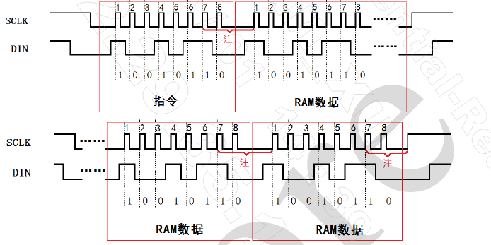
Start Signal: It is recommended to maintain an interval of at least 100ns between the data falling edge and the clock falling edge.
Stop Signal: It is recommended to maintain an interval of at least 100ns between the data rising edge and the clock rising edge.
There should be a minimum of 1us interval between the previous stop signal and the next start signal.
The DATA signal should transition after 250ns following the CLK signal’s falling edge.
Function

State Name |
Description |
|---|---|
CTL_IDLE |
idle state, when r_i2c_tx_start=1, state jump to CTL_START |
CTL_START |
start state, gen start signal, set SDA=0, SCLK =1, when div_cnt==r_i2c_clk_div*2-1, state jump to CTL_WORK |
CTL_WORK |
work state, gen SCLK/SDA and output, when gen all data, state jump to CTL_STOP |
CTL_STOP |
stop state, gen stop signal, set SDA=0, SCLK=1, when div_cnt==r_i2c_clk_div*2-1, state jump to CTL_IDLE |

IDLE State: The circuit is not operational, and SCLK/SDA remains at a logic high level.
START State: Upon receiving the software start signal, r_i2c_tx_status is pulled low, and div_cnt starts counting. The count value is set to r_i2c_clk_div2-1, with r_i2c_clk_div having a minimum value of 2. SDA is immediately pulled low, and SCLK is lowered after a delay of r_i2c_clk_div2-1 cycles, generating the start flag.
After div_cnt completes one cycle, the first psedu_fifo_read signal is generated, reading 1 byte of data from the LED buffer.
WORK State: Based on the 1-byte data read from the LED buffer and the clock division factor, the corresponding SCLK and SDA signals are generated. After pushing each byte of data, a new psedu_fifo_read signal is generated to read the next 1-byte of data until the specified length of data is read from the register.
STOP State: After reading all the data, SCLK is raised, and once div_cnt completes one cycle, SDA is raised, generating the stop flag. The system then enters the IDLE state, and r_i2c_tx_status is set to high.
RAM Structure
The architecture of RAM is show below. The total size is 256 bytes, including 128 bytes LEDC register, 64 bytes RAM0 and 64 bytes RAM1. SW can only write and clear the block of RAM that HW is not used. When SW needs to write the RAM, it’s better to read registers to know which block of RAM that HW is used.

Operation Flow
Pseudo I2C
Read r_i2c_tx_status 0x08[6] to determine the current status of the I2C operation. If it’s 1, it indicates idle and can be operated
Write r_psedo_i2c_en 0x08[7]=1 to enable the I2C function.
Write 0x10[31:0]=0xa5a5a5a5 to disable register protection.
Write a certain quantity of 8-bit data to RAM and set r_i2c_data_num 0x08[14:8] to the number of data written to RAM. Also, write r_i2c_clk_div 0x08[5:0] to configure the clock divider, with a minimum value of 2.
First, write 0x0c[31:0]=0x69696969, then write 0x0c[31:0]=0x96969696. Trigger the hardware to read data from RAM and display it. Also, set r_seq_pass_flag 0x00[20] to 1, indicating that the sequence is correct. Clear it after reading the corresponding register once.
Write 0x10[31:0] with a non-0xa5a5a5a5 value to enable register protection.
The I2C enters the working state, r_i2c_status is set to 0. When all data is displayed, r_i2c_status is set to 1, and it returns to idle.
Registers
Base address: 4080_B200
Name |
Address offset |
Access |
Description |
|---|---|---|---|
000h |
R/W |
||
004h |
R/W |
||
008h |
R/W |
||
00Ch |
R/W |
||
010h |
R/W |
||
080h |
R/W |
REG_LED_PALY_CTL0
Size : 32
Address offset : 000h
Read/write access : R/W
Bit |
Symbol |
Access |
Reset |
Description |
|---|---|---|---|---|
31:24 |
RSVD |
R |
- |
Reserved |
23 |
R_LED_ROW_DISP_INV |
R/W |
0 |
|
22 |
R_LED_COL_DISP_INV |
R/W |
0 |
|
21 |
R_LED_DISPLAY_MODE |
R/W |
0 |
|
20 |
R_SEQ_PASS_FLAG |
R |
0 |
|
19 |
R_LED_ROW_IDLE_STATUS |
R/W |
1 |
|
18 |
R_LED_COLUMN_IDLE_STATUS |
R/W |
1 |
|
17 |
R_LED_BUF_CLEAR |
R/W |
0 |
Write 1 generate one pulse. Clear and reset ram data |
16:9 |
R_OVERLAP_TIME |
R/W |
0x3 |
Time is r_overlap_time +1, delay beweent stage, unit 4M cloc k |
8:6 |
R_LED_ROW |
R/W |
0 |
Led row number - 1 |
5:3 |
R_LED_COLUMN |
R/W |
0 |
Led column number - 1 |
2 |
LEDBUF_SWITCH_ON |
R |
0 |
|
1 |
LEDBUF_FLAG |
R |
1 |
|
0 |
R_LED_DISPLAY_EN |
R/W |
0 |
|
REG_LED_PALY_CTL1
Size : 32
Address offset : 004h
Read/write access : R/W
Bit |
Symbol |
Access |
Reset |
Description |
|---|---|---|---|---|
31:24 |
RSVD |
R |
- |
Reserved |
23:16 |
R_LED_BLANK_TIME |
R/W |
0x3B |
Time is r_led_blank_time +1 , unit 4M clock |
15:13 |
RSVD |
R |
- |
Reserved |
12:0 |
R_LED_PWM_TIME |
R/W |
0x5 |
One stage time of a frame, unit 255*250ns |
REG_PSDO_I2C_CTL
Size : 32
Address offset : 008h
Read/write access : R/W
Bit |
Symbol |
Access |
Reset |
Description |
|---|---|---|---|---|
31:16 |
RSVD |
R |
- |
Reserved |
15 |
DUMMY |
R/W |
0 |
Dummy |
14:8 |
R_I2C_DATA_NUM |
R/W |
0 |
Psdo i2c data num, unit: byte |
7 |
R_PSEDO_I2C_EN |
R/W |
0 |
Indicate psedo i2c in working, only when this bit=1 can acce ss psedo i2c ram |
6 |
R_I2C_TX_STATUS |
R |
1 |
|
5:0 |
R_I2C_CLK_DIV |
R/W |
0 |
Clock division factor = r_i2c_clk_div * 2, minimum value is 2 |
REG_SEQUENCE_CHECK0
Size : 32
Address offset : 00Ch
Read/write access : R/W
Bit |
Symbol |
Access |
Reset |
Description |
|---|---|---|---|---|
31:0 |
R_SEQ_CHK0 |
R/W |
0 |
Sequence check, when this field first write 0x69696969, then write 0x96969696, tirgger led/i2c work |
REG_SEQUENCE_CHECK1
Size : 32
Address offset : 010h
Read/write access : R/W
Bit |
Symbol |
Access |
Reset |
Description |
|---|---|---|---|---|
31:0 |
R_SEQ_CHK1 |
R/W |
0 |
Register protect sequence check, when this field = 0xa5a5a5a 5, enable access protect register |
REG_LED_RAM
Size : 32
Address offset : 080h
Read/write access : R/W
Bit |
Symbol |
Access |
Reset |
Description |
|---|---|---|---|---|
31:0 |
R_LED_RAM_DATA |
R/W |
0 |
4100_9280~4100_92FF 128bytes 4100_9280~4100_92BF,64bytes used for led display 4100_9280~4100_92C0,65bytes used for psdo i2c |