Introduction
The infrared radiation (IR) is mainly designed to process IR signal with carrier frequency under 500kHz. The hardware IP supports hardware modulation which can be used on the IR Tx transmission. It also can detect the period of a continuous high/low level signal, and record in Rx FIFO, and then the software can recognize a received IR signal serial and process it.
The IR IP supports 2 types of IR Rx front end, IR diode or IR receiver module. With the IR diode front end, the IR Rx input signal still has carrier clock on it. So the software needs to do the de-modulation, which increases the CPU load. If the IR Rx front end is an IR receiver module, the carrier is filtered by the IR receiver module. So there isn’t a carrier on the IR Rx input signal.
To simplify the IR signal model, a serial of IR signals is divided into several symbols. A symbol is defined as several carrier clock cycles in a certain period which is called carrier symbol, or a continuous of high/low level signal for a certain period which is called space symbol. Carrier symbol is a real signal that spreads in the air; space symbol is the signal before modulation or after de-modulation.

In Tx mode, firstly, software programs modulation parameter to generate a fixed frequency carrier, and then programs Tx FIFO to generate space symbols. Tx module modulates and transmits those IR signals. The IR Tx flow is illustrated in the following figure.

In Rx mode, if Rx front end is IR receiver module, the signals captured by IR IP core are space symbol; if Rx front end is IR diode, the signals captured by IR IP core are carrier symbols. The software process flow is divided into de-modulation and decoding. If IR diode is used, received IR signals must be de-modulated firstly. The IR Rx flow is illustrated in the following figure.

Features
Wide range of carrier frequency: from 25kHz to 500kHz
Customizable duty by users
Optional IR diode input
Optional IR receiver module input
32*4 bytes Tx FIFO
32*4 bytes Rx FIFO
Configurable Tx carrier frequency
Configurable Tx carrier duty cycle
Half-duplex mode
Block diagram
The block diagram of IR is shown below:

Scaler: for Tx carrier frequency or Rx sample frequency generated from SCLK (100MHz).
Carrier Generator: Tx carrier symbol with fixed carrier duty number.
Modulation: modulates space symbol to carrier symbol.
Glitch Filer: IR rx filter to avoid glitches when receiving data from bus.
FIFO: IR Tx and Rx FIFO. Tx FIFO is used to generate Tx carrier symbol count and state of Tx data; Rx FIFO is used to save the data received from bus, for software programs.
Interrupt Control: generates interrupt for CPU handler.
Register: contains the configuration of IR module, it’s the interface with software.
Functional Description
Scaler
Tx mode
The division clock after scaler is carrier frequency.
The default clock frequency is 40MHz.
Supported Clock Source Selection: SYS_PLL
The default clock frequency is 100MHz.
Note
Ensure the clock synchronization with hbus_clock.
The default clock frequency is 40MHz.
Note
Ensure the clock synchronization with peri_lclk.
For example, SCLK=100MHz, carrier frequency = 455kHz, IR_DIV_NUM = (100M/455k) - 1.
Rx mode
The division clock after scaler is sampling clock. Combining Rx counter with sampling clock, software can analyze high or low level signal duration.
For example, Rx sampling clock is 10MHz, Rx count is 0x800000FF, indicating that high level duration is 255us (where bit[31] indicates input level: 1 = high; 0 = low).
Data Format
This section introduces the data format of Tx FIFO and Rx FIFO.
IR Tx
To send IR data, you should write the data into IR Tx FIFO register, so it’s important to understand the data format to be sent to Tx FIFO register. Before sending data, you should convert the data into the appropriate format that Tx FIFO register can recognize. The size of Tx FIFO register is 32 bits, where:
- Bit[31]:
indicates data level, where 1 is high level and 0 is low level.
- Bit[30]:
indicates the data end flag, where 1 is the last package, and 0 is the normal package.
- Bit[29:28]:
indicates Tx compensation mode, where 00 using Tsample and 11 using Tcomp_clk.
- Bit[27:0]:
indicates the number of carrier cycles.
Let represents the carrier frequency (the unit of is Hz), represents the duration of carrier or no carrier symbol (the unit of is us). Then,
Taking NEC protocol for example, the carrier frequency is 38kHz. The format of NEC is shown in the following figure. The NEC format consists of 2 start symbols, 64 data symbols and 1 stop symbol.
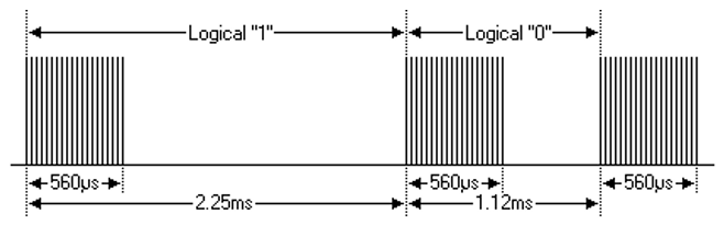
To send logical ‘1’, you should write two data into Tx FIFO register.
For the first data, bit[31] = 1, bit[30] = 0, bit[27:0] = 38*560/1000 = 21.
For the second data, bit[31] = 0, bit[30] = 0, bit[27:0] = 38*(2250-560)/1000 = 64.
To send logical ‘0’, you should write two data into Tx FIFO register.
For the first data, bit[31] = 1, bit[30] = 0, bit[27:0] = 38*560/1000 = 21.
For the second data, bit[31] = 0, bit[30] = 0, bit[27:0] = 38*(1120-560)/1000 =21.
At last, you need to send the stop symbol. In this symbol, set bit[30] = 1 because the stop symbol indicates the data end of the current transmission.
IR Rx
To receive IR data, you should read the data in Rx FIFO register, so it’s important to understand the data format to be received in Rx FIFO register. The size of Rx FIFO register is 32 bits, where:
Bit[31] indicates data level, where 1 is high level and 0 is low level.
Bit[30:0] stores the data to be received and the data format is cycle duration. Let fsampling represents the sampling frequency (the unit of fsampling is kHz). Tlevel represents the duration of each high/low level (the unit of Tlevel is μs). Then,
With the use of Tlevel, you can do further processing to get the information you need.
Tx Compensation Mechanism
Tx waveforms are composed of some carrier symbols and no carrier symbols. Software calculates the duration of a certain symbol by application specification (such as NEC). But no carrier symbols cannot be divisible by carrier frequency accurately. If there is no effective compensation mechanism, the error will increase. So Tx compensation is proposed and used in IR Tx to decrease the error.
In most scenarios, it is not necessary to adopt a compensation mechanism. Therefore, if you are not interested in the compensation mechanism, just skip this section. Next, we would introduce the application of compensation mechanism.
Take NEC application for example, the TX NEC waveform shown in the following figure is with fcarrier = 38kHz, and duty = 1/3. The system clock is 100MHz.
For 38kHz carrier frequency:
Compensation frequency fcomp is a dependent clock, you can set fcomp to any value you want. In this example, we set fcomp = 1MHz, so

We divide this waveform into four symbols: 560μs carrier symbol, 1690μs (2250μs ~ 560μs) no carrier symbol, 560μs carrier symbol, and 560μs (1120μs ~ 560μs) no carrier symbol. Compare the above two calculating methods, we can find that by using a compensation mechanism, the accuracy can be improved.
Item |
Normal Tx (IR_TX_COMPENSATION = 0) |
Tx compensation (IR_TX_COMPENSATION = 3) |
|---|---|---|
1st cycle |
560μs ≈ 21*26.31 + 8.77 = 561.26μs |
560μs ≈ 21*26.31 + 8.77 = 561.26μs |
2nd cycle |
1690μs ≈ 64*26.31+(26.31-8.77)=1701.38μs |
1690μs ≈ (26.31-8.77) + 1673*1 = 1690.54μs |
3rd cycle |
560μs ≈ 21*26.31+ 8.77 = 561.28μs |
560μs ≈ 21*26.31 + 8.77 = 561.26μs |
4th cycle |
560μs ≈ 21*26.31+(26.31-8.77)=570.05μs |
560μs ≈ (26.31-8.77) + 543 * 1 = 560.54μs |
TX FIFO data value |
0x80000015, 0x00000040 0x80000015, 0x00000015 |
0x80000015, 0x30000689 0x80000015, 0x3000021F |
Note
The compensation mechanism can only be used for no carrier symbol.
Compensation method 1 (IR_TX_COMPENSATION=1) and method 2 (IR_TX_COMPENSATION=2) are not recommended. If you want to use a compensation mechanism, refer to method 3 (IR_TX_COMPENSATION=3).
If IR_TX_DE_INVERSE enabled, then make sure TX compensation divider (0xC [11:0]) no less than TX duty number(0X4[27:16]).
Rx Glitch Filter
There is a glitch filter before IR input sampling, and the glitch filter can be set to 20ns, 30ns, 40ns, 50ns, 60ns, 70ns, 80ns or 90ns.
Interrupt
Each mode has some interrupt flags, as listed below, and these interrupt sources can be enabled, masked, or cleared individually.
Mode |
Interrupt flag |
Description |
|---|---|---|
Tx mode |
IR_TX_FIFO_OVER_INT |
When Tx FIFO is full, writing data to Tx FIFO triggers this interrupt. |
Tx mode |
IR_TX_FIFO_LEVEL_INT |
When Tx FIFO offset decreases from threshold value to threshold value − 1, this interrupt is triggered. |
Tx mode |
IR_TX_FIFO_EMPTY_INT |
When Tx FIFO offset decreases from 1 to 0, this interrupt is triggered. |
Rx mode |
IR_RX_FIFO_ERROR_INT |
When Rx FIFO is empty, reading data from Rx FIFO triggers this interrupt. |
Rx mode |
IR_RX_CNT_THR_INT |
When given input level duration exceeds Rx counter threshold, this interrupt is triggered. |
Rx mode |
IR_RX_CNT_OF_INT |
When Rx counter overflow without IR_RX_CNT_THR_INT happens. |
Rx mode |
IR_RX_FIFO_OF_INT |
When Rx FIFO is full, Rx more data from IR input pin triggers this interrupt. |
Rx mode |
IR_RX_FIFO_LEVEL_INT |
When Rx FIFO offset increases from threshold value to threshold value + 1, this interrupt is triggered. |
Rx mode |
IR_RX_FIFO_FULL_INT |
When Rx FIFO is full, this interrupt is triggered. |
Registers
Name |
Address offset |
Access |
Description |
|---|---|---|---|
000h |
R/W |
||
004h |
R/W |
||
008h |
R |
||
00Ch |
R/W |
||
010h |
R/W |
||
014h |
R/W |
||
018h |
R/W |
||
01Ch |
R |
||
020h |
R/W |
||
024h |
R/W |
||
028h |
R |
||
02Ch |
R |
||
030h |
R |
REG_IR_CLK_DIV
Name : IR clock division register
Size : 32
Address offset : 000h
Read/write access : R/W
Bit |
Symbol |
Access |
Reset |
Description |
|---|---|---|---|---|
31:12 |
RSVD |
R |
- |
Reserved |
11:0 |
IR_CLK_DIV |
R/W |
0x0 |
IR_CLK = IO_CLK/(1 + IR_CLK_DIV)
For example: sys_clk = 40MHz, modulation_freq = 455kHz, IR_D IV_NUM = (sys_clk/modulation_freq) - 1
IR_DIV_NUM = (sys_clk/sample clock) - 1 For example: sample clock = 40MHz, IR_DIV_NUM = 0; sample cl ock = 20MHz, IR_DIV_NUM = 1 |
REG_IR_TX_CONFIG
Name : IR Tx configuration register
Size : 32
Address offset : 004h
Read/write access : R/W
Bit |
Symbol |
Access |
Reset |
Description |
|---|---|---|---|---|
31 |
IR_MODE_SEL |
R/W |
0x0 |
|
30 |
IR_TX_START |
R/W |
0x0 |
|
29:28 |
RSVD |
R |
- |
Reserved |
27:16 |
IR_TX_DUTY_NUM |
R/W |
0x0 |
Duty cycle setting for modulation frequency For example: for 1/3 duty cycle, IR_DUTY_NUM = (IR_DIV_NUM+1 )/3 Note Set this value equals to IR_DIV_NUM to generate 100% duty waveform. |
15 |
RSVD |
R |
- |
Reserved |
14 |
IR_TX_OUTPUT_INVERSE |
R/W |
0x0 |
|
13 |
IR_TX_DE_INVERSE |
R/W |
0x0 |
|
12:8 |
IR_TX_FIFO_LEVEL_TH |
R/W |
0x0 |
Tx FIFO interrupt threshold. When Tx FIFO depth = < threshold value, interrupt is trigger ed. |
7 |
RSVD |
R |
- |
Reserved |
6 |
IR_TX_IDLE_STATE |
R/W |
0x0 |
Tx output state in idle
|
5 |
IR_TX_FIFO_OVER_INT_MASK |
R/W |
0x0 |
Tx FIFO overflow interrupt
|
4 |
IR_TX_FIFO_OVER_INT_EN |
R/W |
0x0 |
Tx FIFO overflow interrupt
|
3 |
IR_TX_FIFO_LEVEL_INT_MASK |
R/W |
0x0 |
Tx FIFO level interrupt
|
2 |
IR_TX_FIFO_EMPTY_INT_MASK |
R/W |
0x0 |
Tx FIFO empty interrupt
|
1 |
IR_TX_FIFO_LEVEL_INT_EN |
R/W |
0x0 |
Tx FIFO level interrupt When Tx FIFO offset <= threshold value, interrupt is trigger ed.
|
0 |
IR_TX_FIFO_EMPTY_INT_EN |
R/W |
0x0 |
Tx FIFO empty interrupt
|
REG_IR_TX_SR
Name : IR Tx FIFO and interrupt status register
Size : 32
Address offset : 008h
Read/write access : R
Bit |
Symbol |
Access |
Reset |
Description |
|---|---|---|---|---|
31:16 |
RSVD |
R |
- |
Reserved |
15 |
IR_TX_FIFO_EMPTY |
R |
0x0 |
|
14 |
IR_TX_FIFO_FULL |
R |
0x0 |
|
13:8 |
IR_TX_FIFO_OFFSET |
R |
0x0 |
Tx FIFO offset is from 0 to 32. Note After Tx last packet, hardware can’t clear Tx FIFO offset . |
7:5 |
RSVD |
R |
- |
Reserved |
4 |
IR_TX_STATUS |
R |
0x0 |
|
3 |
RSVD |
R |
- |
Reserved |
2 |
IR_TX_FIFO_OVER_INT_STATUS |
R |
0x0 |
Tx FIFO overflow interrupt
|
1 |
IR_TX_FIFO_LEVEL_INT_STATUS |
R |
0x0 |
When Tx FIFO offset <= threshold value, interrupt is trigger ed.
|
0 |
IR_TX_FIFO_EMPTY_INT_STATUS |
R |
0x0 |
Tx FIFO empty interrupt
|
REG_IR_TX_COMPE_DIV
Name : IR Tx compensation division register
Size : 32
Address offset : 00Ch
Read/write access : R/W
Bit |
Symbol |
Access |
Reset |
Description |
|---|---|---|---|---|
31:12 |
RSVD |
R |
- |
Reserved |
11:0 |
TX_COMPE_DIV |
R/W |
0x0 |
IR_TX_CLK_Period = SCLK/(TX_COMPE_DIV + 1) |
REG_IR_TX_INT_CLR
Name : IR Tx FIFO and interrupt clear register
Size : 32
Address offset : 010h
Read/write access : R/W
Bit |
Symbol |
Access |
Reset |
Description |
|---|---|---|---|---|
31:4 |
RSVD |
R |
- |
Reserved |
3 |
IR_TX_FIFO_OVER_INT_CLR |
R/W |
Tx FIFO overflow interrupt Write 1 to clear |
|
2 |
IR_TX_FIFO_LEVEL_INT_CLR |
R/W |
When Tx FIFO offset <= threshold value, interrupt is trigger ed. Write 1 to clear |
|
1 |
IR_TX_FIFO_EMPTY_INT_CLR |
R/W |
Tx FIFO empty interrupt Write 1 to clear |
|
0 |
IR_TX_FIFO_CLR |
R/W |
Write 1 to clear Tx FIFO |
REG_IR_TX_FIFO
Name : IR Tx FIFO register
Size : 32
Address offset : 014h
Read/write access : R/W
Bit |
Symbol |
Access |
Reset |
Description |
|---|---|---|---|---|
31 |
IR_TX_DATA_TYPE |
R/W |
0 |
Data type
|
30 |
IR_TX_DATA_END_FLAG |
R/W |
0 |
|
29:28 |
IR_TX_COMPENSATION |
R/W |
0 |
|
27:0 |
IR_TX_DATA_TIME |
R/W |
0 |
Real active time = (IR_TX_DATA_TIME + 1) * IR_TX_CLK_Period |
REG_IR_RX_CONFIG
Name : IR Rx configuration register
Size : 32
Address offset : 018h
Read/write access : R/W
Bit |
Symbol |
Access |
Reset |
Description |
|---|---|---|---|---|
31:29 |
RSVD |
R |
- |
Reserved |
28 |
IR_RX_START |
R/W |
0x0 |
|
27 |
IR_RX_START_MODE |
R/W |
0x0 |
|
26 |
IR_RX_MAN_START |
R/W |
0x0 |
If IR_RX_TRIGGER_MODE =0, writing 1 means starting to check the waveform. |
25:24 |
IR_RX_TRIGGER_MODE |
R/W |
0x0 |
|
23:21 |
IR_RX_FILTER_STAGETX |
R/W |
0x0 |
… |
20 |
RSVD |
R |
- |
Reserved |
19 |
IR_RX_FIFO_ERROR_INT_MASK |
R/W |
0x0 |
Rx FIFO error read interrupt When Rx FIFO is empty, read Rx FIFO and trigger interrupt.
|
18 |
IR_RX_CNT_THR_INT_MASK |
R/W |
0x0 |
Rx count threshold interrupt
|
17 |
IR_RX_FIFO_OF_INT_MASK |
R/W |
0x0 |
Rx FIFO overflow
|
16 |
IR_RX_CNT_OF_INT_MASK |
R/W |
0x0 |
RX counter overflow
|
15 |
IR_RX_FIFO_LEVEL_INT_MASK |
R/W |
0x0 |
Rx FIFO level interrupt
When Rx FIFO offset >= threshold value, this interrupt is tr iggered. |
14 |
IR_RX_FIFO_FULL_INT_MASK |
R/W |
0x0 |
Rx FIFO full interrupt
|
13 |
IR_RX_FIFO_DISCARD_SET |
R/W |
0x0 |
When FIFO is full, new data is send to FIFO.
|
12:8 |
IR_RX_FIFO_LEVEL_TH |
R/W |
0x0 |
Rx FIFO interrupt threshold When Rx FIFO depth > threshold value, this interrupt is trig gered. |
7:6 |
RSVD |
R |
- |
Reserved |
5 |
IR_RX_FIFO_ERROR_INT_EN |
R/W |
0x0 |
Rx FIFO error read interrupt When Rx FIFO is empty, reading the Rx FIFO triggers this int errupt.
|
4 |
IR_RX_CNT_THR_INT_EN |
R/W |
0x0 |
Rx count threshold interrupt
|
3 |
IR_RX_FIFO_OF_INT_EN |
R/W |
0x0 |
RX FIFO overflow
|
2 |
IR_RX_CNT_OF_INT_EN |
R/W |
0x0 |
RX counter overflow
|
1 |
IR_RX_FIFO_LEVEL_INT_EN |
R/W |
0x0 |
Rx FIFO level interrupt When Rx FIFO offset >= threshold value, this interrupt is tr iggered.
|
0 |
IR_RX_FIFO_FULL_INT_EN |
R/W |
0x0 |
Rx FIFO full interrupt
|
REG_IR_RX_SR
Name : IR Rx FIFO and interrupt status register
Size : 32
Address offset : 01Ch
Read/write access : R
Bit |
Symbol |
Access |
Reset |
Description |
|---|---|---|---|---|
31:18 |
RSVD |
R |
- |
Reserved |
17 |
IR_RX_FIFO_EMPTY |
R |
0x0 |
|
16 |
IR_RX_FIFO_FULL |
R |
0x0 |
|
15:14 |
RSVD |
R |
- |
Reserved |
13:8 |
IR_RX_FIFO_OFFSET |
R |
0x0 |
Rx FIFO offset |
7 |
IR_RX_STATE |
R |
0x0 |
|
6 |
RSVD |
R |
- |
Reserved |
5 |
IR_RX_FIFO_ERROR_INT_STATUS |
R |
0x0 |
Rx FIFO error read interrupt status When Rx FIFO is empty, reading the Rx FIFO triggers this int errupt.
|
4 |
IR_RX_CNT_THR_INT_STATUS |
R |
0x0 |
Rx count threshold interrupt status
|
3 |
IR_RX_FIFO_OF_INT_STATUS |
R |
0x0 |
Rx FIFO overflow interrupt status
|
2 |
IR_RX_CNT_OF_INT_STATUS |
R |
0x0 |
Rx counter overflow interrupt status
|
1 |
IR_RX_FIFO_LEVEL_INT_STATUS |
R |
0x0 |
Rx FIFO level interrupt status
|
0 |
IR_RX_FIFO_FULL_INT_STATUS |
R |
0x0 |
Rx FIFO full interrupt status
|
REG_IR_RX_INT_CLR
Name : IR Rx FIFO and interrupt clear register
Size : 32
Address offset : 020h
Read/write access : R/W
Bit |
Symbol |
Access |
Reset |
Description |
|---|---|---|---|---|
31:9 |
RSVD |
R |
- |
Reserved |
8 |
IR_RX_FIFO_CLR |
R/W |
Write 1 to clear Rx FIFO |
|
7:6 |
RSVD |
R |
- |
Reserved |
5 |
IR_RX_FIFO_ERROR_INT_CLR |
R/W |
Rx FIFO error read interrupt Write 1 to clear |
|
4 |
IR_RX_CNT_THR_INT_CLR |
R/W |
Rx count threshold interrupt Write 1 to clear |
|
3 |
IR_RX_FIFO_OF_INT_CLR |
R/W |
Rx FIFO overflow interrupt Write 1 to clear |
|
2 |
IR_RX_CNT_OF_INT_CLR |
R/W |
Rx counter overflow interrupt Write 1 to clear |
|
1 |
IR_RX_FIFO_LEVEL_INT_CLR |
R/W |
Rx FIFO level interrupt Write 1 to clear |
|
0 |
IR_RX_FIFO_FULL_INT_CLR |
R/W |
Rx FIFO full interrupt Write 1 to clear |
REG_IR_RX_CNT_INT_SEL
Name : IR Rx count threshold configure register
Size : 32
Address offset : 024h
Read/write access : R/W
Bit |
Symbol |
Access |
Reset |
Description |
|---|---|---|---|---|
31 |
IR_RX_CNT_THR_TRIGGER_LV |
R/W |
0x0 |
Trigger level
|
30:0 |
IR_RX_CNT_THR |
R/W |
0x0 |
31-bits threshold |
REG_IR_RX_FIFO
Name : IR Rx FIFO register
Size : 32
Address offset : 028h
Read/write access : R
Bit |
Symbol |
Access |
Reset |
Description |
|---|---|---|---|---|
31 |
IR_RX_LEVEL |
R |
0x0 |
Rx Level
|
30:0 |
IR_RX_CNT |
R |
0x0 |
31-bits cycle duration |
REG_IR_VERSION
Name : IR IP version register
Size : 32
Address offset : 02Ch
Read/write access : R
Bit |
Symbol |
Access |
Reset |
Description |
|---|---|---|---|---|
31:0 |
IR_VERSION |
R |
0x1410150A |
IR IP version |
REG_IR_DUMMY
Name : Ir Dummy Register
Size : 32
Address offset : 030h
Read/write access : R
Bit |
Symbol |
Access |
Reset |
Description |
|---|---|---|---|---|
31:16 |
RSVD |
R |
- |
Reserved |
15:0 |
DUMMY |
R |
0x0 |
Rsvd for hw |