Introduction
This chapter describes the I2C interface peripherals, referred to as I2C.
The I2C bus interface handles communications between the chip and the serial I2C bus. It controls all I2C bus-specific sequencing, protocol, arbitration and timing. The design of I2C aims on sensor hub application in low-power or battery-powered productions. Essential features of I2C bus protocol should be provided for acquiring or controlling external sensor data.
Features
The I2C has the following features:
Two-wire I2C serial interface – a serial data line (SDA) and a serial clock (SCL)
Three speed modes:
Standard Speed (SS), up to 100Kbps
Fast Speed (FS), up to 400Kbps
High Speed (HS), up to 3.4Mbps
I2C interface: x3
I2C0 is on LS platform (LS_APB_CLK, 10MHz), only supports Standard Speed and Fast Speed modes.
The IP clk of I2C1 and I2C2 is 40M. I2C1 and I2C2 are both on HP platform (HP_AHB_CLK, 100MHz), support all speed modes.
I2C interface: x2
The IP clk of I2C0 and I2C1 is 120M. I2C0 and I2C1 can be accessed by both KM4 and KR4, and support all speed modes.
I2C interface: x2
The IP clk of I2C0 and I2C1 is 120M. I2C0 and I2C1 can be accessed by both KM4 and KR4, and support all speed modes.
I2C interface: x2
The IP clk of I2C0 and I2C1 is 120M. I2C0 and I2C1 can be accessed by both KM4 and KR4, and support all speed modes.
I2C interface: x3
I2C0 is on LS platform (LS_APB_CLK, 20MHz), only supports Standard Speed and Fast Speed modes.
I2C1 and I2C2 are on HP platform (HP_AHB_CLK, 100MHz), support all speed modes.
I2C interface: x3
I2C0 is on LS platform (LS_APB_CLK, 10MHz), only supports Standard Speed and Fast Speed modes.
I2C1 and I2C2 are on HP platform (HP_AHB_CLK, 100MHz), support all speed modes.
Master or Slave I2C operation
Transmitter or Receiver
Transmit and receive FIFOs with depth of 16 and width of 12-bit
Multi-master ability including bus arbitration scheme
Clock stretch in master/slave mode
7-bit or 10-bit addressing mode, 7-bit or 10-bit combined format transfer
Manual START/RESTART/STOP bit control
Supports General Call, NULL DATA, START BYTE transfer protocol
Component parameters for configurable software driver support (programmable SDA hold time, slave address, SCL duty cycle, etc.)
Filter to eliminate the glitches on the signal of SDA and SCL, programmable digital noise Filter
Status flags (Bus busy flag, activity flag, FIFO status flag, etc.) and Error flags (arbitration lost, acknowledge failure, etc.)
Slave Mode Dual Own Address
Slave 1 supports 7-bit or 10-bit address mode
Slave 2 only supports 7-bit address mode
Operation mode:
Polling
Interrupt
Block Diagram
The block diagram of I2C is illustrated below. The following defines the file names and functions of the blocks.
AMBA Bus Interface: Takes the APB interface signals and translates them into a common generic interface that allows the register file to be bus protocol-agnostic.
Register File: Contains configuration registers and is the interface with the software.
Slave State Machine: Follows the protocol for a slave and monitors bus for address match.
Master State Machine: Generates the I2C protocol for the master transfers.
Clock Generator: Calculates the required timing to do the following:
Generate the SCL clock when configured as a master
Check for bus idle
Generate a START and a STOP
Setup the data and hold the data
Rx Shift: Takes data into the design and extracts it in byte format.
Tx Shift: Presents data supplied by CPU for transfer on the I2C bus.
Rx Filter: Detects the events in the bus; for example, start, stop and arbitration lost.
Toggle: Generates pulses on both sides and toggles to transfer signals across clock domains.
Synchronizer: Transfers signals from one clock domain to another.
DMA Interface: Generates the handshaking signals to the central DMA controller in order to automate the data transfer without CPU intervention.
Interrupt Controller: Generates the raw interrupt and interrupt flags, allowing them to be set and cleared.
Rx FIFO/Tx FIFO: Holds the RX FIFO and TX FIFO register banks and controllers, along with their status levels.

Functional Description
This section describes the functional behavior of the I2C in more details.
Overview
The I2C bus is a two-wire serial interface, consisting of a serial data line (SDA) and a serial clock (SCL). These wires carry information between the devices connected to the bus. Each device is recognized by a unique address and can operate as either a “transmitter” or “receiver,” depending on the function of the device. Devices can also be considered as masters or slaves when performing data transfers. A master is a device that initiates a data transfer on the bus and generates the clock signals to permit that transfer. At that time, any device addressed is considered a slave.
Note
The I2C must only be programmed to operate in either master or slave mode only. Operating as master and slave simultaneously is not supported.
Any I2C device can be attached to an I²C-bus and every device can talk with any master, passing information back and forth. There needs to be at least one master (such as a microcontroller or DSP) on the bus but there can be multiple masters, which require them to arbitrate for ownership. Multiple masters and arbitration are explained later in this section. An example schematic with one master and three slave nodes is illustrated below.

I2C Terminology
The following terms are used throughout this chapter and are defined as below.
I2C Bus Terms
The following terms relate to what is the role of the I2C device and how it interacts with other I2C devices on the bus.
Transmitter – the device that sends data to the bus. A transmitter can either be a device that initiates the data transmission to the bus (a master-transmitter) or responds to a request from the master to send data to the bus (a slave-transmitter).
Receiver – the device that receives data from the bus. A receiver can either be a device that receives data on its own request (a master-receiver) or in response to a request from the master (a slave-receiver).
Master -– the component that initializes a transfer (START command), generates the clock (SCL) signal and terminates the transfer (STOP command). A master can be either a transmitter or a receiver.
Slave – the device addressed by the master. A slave can be either receiver or transmitter. These concepts are illustrated below.
Multi-master – the ability for more than one master to co-exist on the bus at the same time without collision or data loss.
Arbitration – the predefined procedure that authorizes only one master at a time to take control of the bus.
Synchronization – the predefined procedure that synchronizes the clock signals provided by two or more masters.
SDA – data signal line (Serial Data)
SCL – clock signal line (Serial Clock)

Bus Transfer Terms
The following terms are specific to data transfers that occur to/from the I2C bus.
START (RESTART) – data transfer begins with a START or RESTART condition. The level of the SDA data line changes from high to low, while the SCL clock line remains high. When this occurs, the bus becomes busy.
STOP – data transfer is terminated by a STOP condition. This occurs when the level on the SDA data line passes from the low state to the high state, while the SCL clock line remains high. When the data transfer has been terminated, the bus is free or idle once again. The bus stays busy if a RESTART is generated instead of a STOP condition.
Note
START and RESTART conditions are functionally identical.
I2C Behavior
The I2C can be controlled via software to be either:
An I2C master only, communicating with other I2C slaves; OR
An I2C slave only, communicating with one more I2C masters.
The master is responsible for generating the clock and controlling the transfer of data. The slave is responsible for either transmitting or receiving data to/from the master. The acknowledgement of data is sent by the device that is receiving data, which can be either a master or a slave. As mentioned previously, the I2C protocol also allows multiple masters to reside on the I2C bus and uses an arbitration procedure to determine bus ownership.
Each slave has a unique address that is determined by the system designer. When a master wants to communicate with a slave, the master transmits a START/RESTART condition that is then followed by the slave’s address and a control bit (R/W) to determine if the master wants to transmit data or receive data from the slave. The slave then sends an acknowledge (ACK) pulse after the address.
If the master (master-transmitter) is writing to the slave (slave-receiver), the receiver gets one byte of data. This transaction continues until the master terminates the transmission with a STOP condition. If the master is reading from a slave (master-receiver), the slave transmits (slave-transmitter) a byte of data to the master, and the master then acknowledges the transaction with the ACK pulse. This transaction continues until the master terminates the transmission by not acknowledging (NACK) the transaction after the last byte is received, and then the master issues a STOP condition or addresses another slave after issuing a RESTART condition. This behavior is illustrated below.

The I2C is a synchronous serial interface. The SDA line is a bidirectional signal and changes only while the SCL line is low, except for STOP, START, and RESTART conditions. The output drivers are open-drain or open-collector to perform wire-AND functions on the bus. The maximum number of devices on the bus is limited by only the maximum capacitance specification of 400pF. Data is transmitted in byte packages.
START and STOP Generation
Refer to register content for IC_DATA_CMD structure. When operating as an I2C master, putting data into the transmit FIFO causes the I2C to generate a START condition on the I2C bus. Writing a 1 to IC_DATA_CMD [9] causes the hardware to generate a STOP condition on the I2C bus; a STOP condition is not issued if this bit is not set, even if the transmit FIFO is empty. Writing a 1 to IC_DATA_CMD [10] causes the hardware to hold bus after the current data is transmitted and generate a RESTART condition when the next data in FIFO is ready to be transmitted on bus.
When operating as a slave, the I2C does not generate START and STOP conditions, as per the protocol. However, if a read request is made to the I2C, it holds the SCL line low until read data has been supplied to it. This stalls the I2C bus until read data is provided to the slave I2C, or the I2C slave is disabled by writing a 0 to bit0 of the REG_IC_ENABLE.
Combined Formats
Combined format transactions: the data send direction may change during a transfer. For example, a master may send data and then receive data or vice versa without release the I2C bus. The combined format illustrated below.

The I2C supports combined format transactions for both 7-bit or 10-bit addressing modes. The I2C does not support mixed address—that is, a 7-bit address transaction followed by a 10-bit address transaction or vice versa—in combined format transaction.
To initiate combined format transfers, IC_CON. IC_RESTART_EN should be set to 1. With this value set and operating as a master, when the I2C completes an I2C transfer, it checks the transmit FIFO and executes the next transfer. If the direction of this transfer differs from the previous transfer, the combined format is used to issue the transfer. If the transmit FIFO is empty when the current I2C transfer completes, IC_DATA_CMD [9] is checked.
If set to 1, a STOP bit is issued.
If set to 0, the SCL is hold low until the next command is written to the transmit FIFO.
I2C Protocols
START and STOP Conditions
When the bus is idle, both the SCL and SDA signals are pulled high through external pull-up resistors on the bus. When the master wants to start a transmission on the bus, the master issues a START condition. This is defined to be a high-to-low transition of the SDA signal while SCL is 1. When the master wants to terminate the transmission, the master issues a STOP condition. This is defined to be a low-to-high transition of the SDA line while SCL is 1. The following figure shows the timing of the START and STOP conditions. When data is being transmitted on the bus, the SDA line must be stable when SCL is 1.

Addressing Slave Protocol
There are two address formats:
7-bit address format
10-bit address format
7-bit Address Format
During the 7-bit address format, the first seven bits (bit[7:1]) of the first byte set the slave address and the LSB bit (bit[0]) is the R/W bit as shown below. When bit[0] is set to 0, the master write data to the slave. When bit[0] is set to 1, the master read data from the slave.

10-bit Address Format
During 10-bit addressing, two bytes are transferred to set the 10-bit address. The transfer of the first byte contains the following bit definition. The first five bits (bit[7:3]) notify the slaves that this is a 10-bit transfer followed by the next two bits (bit[2:1]), which set the slaves address bits 9:8, and the LSB bit (bit[0]) is the R/W bit. The second byte transferred sets bit[7:0] of the slave address. The following figure shows the 10-bit address format, and the table defines the special purpose and reserved first byte addresses.

Slave address |
R/W bit |
Description |
|---|---|---|
0000 000 |
0 |
General Call Address. I2C places the data in the receive buffer and issues a General Call interrupt. |
0000 000 |
1 |
START byte |
0000 001 |
x |
CBUS address. I2C ignores these accesses. |
0000 010 |
x |
Reserved |
0000 011 |
x |
Reserved |
0000 1XX |
x |
High speed master code |
1111 1XX |
x |
Reserved |
1111 0XX |
x |
10-bit slave addressing |
The I2C does not restrict you from using these reserved addresses. However, if the reserved addresses are used, you may run into incompatibilities with other I2C components.
Transmitting and Receiving Protocol
The master can initiate data transmission and reception to/from the bus, acting as either a master-transmitter or master-receiver. A slave responds to requests from the master to either transmit data or receive data to/from the bus, acting as either a slave-transmitter or slave-receiver, respectively.
Master-Transmitter and Slave-Receiver
All data is transmitted in byte format, with no limit on the number of bytes transferred per data transfer. After the master sends the address and R/W bit or the master transmits a byte of data to the slave, the slave-receiver must respond with the acknowledge signal (ACK). When a slave-receiver does not respond with an ACK pulse, the master aborts the transfer by issuing a STOP condition. The slave must leave the SDA line high so that the master can abort the transfer.
If the master-transmitter is transmitting data as shown below, then the slave-receiver responds to the master-transmitter with an acknowledge pulse after every bytes of data is received.

Master-Receiver and Slave-Transmitter
If the master is receiving data as shown below, then the master responds to the slave-transmitter with an acknowledge pulse after a byte of data has been received, except for the last byte. This is the way the master-receiver notifies the slave-transmitter that this is the last byte. The slave-transmitter relinquishes the SDA line after detecting the No Acknowledge (NACK) so that the master can issue a STOP condition.
For 10-bit address, the transfer progress is also shown below.
Address phase 1: master send {5'b11110, slave address [9:8], 1'b0}; R/W=1'b0 means master will send data in data phase.
Data phase 1: master send slave address [7:0];
A restart is set to indicate the direction toggle of data transfer.
Address phase 2: master send {5'b11110, slave address [9:8], 1'b1}; R/W=1'b1 means master will receive data in data phase.
Data phase 2: master receives data from slave.
When a master does not want to relinquish the bus with a STOP condition, the master can issue a RESTART condition. This is identical to a START condition except it occurs after the ACK pulse. Operating in master mode, the I2C can then communicate with the same slave using a transfer of a different direction.

START BYTE Transfer Protocol
Microcontroller can be connected to I2C-bus in two ways:
Interrupt by START BYTE request: A microcontroller with an on-chip hardware I2C-bus interface can be programed to be only interrupted by requests from the bus. Or
Polling the bus: When the device does not have such an interface, it must constantly monitor the bus. Obviously, the more times the microcontroller monitors, or polls the bus, the less time carrying out its intended function. There is therefore a speed difference between fast hardware device and a relatively slow microcontroller, which relies on software polling.
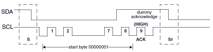
As shown in the figure above, the START BYTE procedure is as follows:
Master generates a START condition.
Master transmits the START byte (0000 0001).
Master transmits the ACK clock pulse. (Present only to conform with the byte handling format used on the bus)
No slave sets the ACK signal to 0.
Master generates a RESTART (R) condition.
After the START condition S has been transmitted by a master which requires bus access, the START byte (0000 0001) is transmitted. Another microcontroller can therefore sample the SDA line at a low sampling rate until one of the seven zeros in the START byte is detected. After detection of this LOW level on the SDA line, the microcontroller can switch to a higher sampling rate to find the repeated START condition Sr which is then used for synchronization.
A hardware receiver will reset on receipt of the repeated START condition Sr and will therefore ignore the START byte.
An acknowledge-related clock pulse is generated after the START byte. This is present only to conform with the byte handling format used on the bus. No device is allowed to acknowledge the START byte.
A hardware receiver does not respond to the START BYTE because it is a reserved address and resets after the RESTART condition is generated.
General Call Transfer Protocol
The general call is for addressing every device connected to the I2C bus. However, if a device doesn’t need any of the data supplied within the general call structure, it can ignore this address by not issuing an acknowledgement. If a device does require this address and behave as a slave-receiver. The second and following bytes will be acknowledged by every slave-receiver capable of handling this data. The following figure gives the General Call address format. The second byte can be:
‘h06: reset and write programmable part of slave address by hardware.
‘h04: write programmable part of slave address by hardware.
7-bit mater address of the hardware master.

When I2C acts as a slave, set IC_ACK_GENERAL_CALL (0x98) bit[0] to 1 to respond with a ACK when it receives a General Call, and a General Call interrupt will be issued. When set this bit to 0, the I2C does not generate General Call interrupts.
NULL DATA Transfer Protocol
NULL DATA transfer is used for some sensors. When IC_DATA_CMD [11] and IC_DATA_CMD [9] is set to 1, I2C would ignore REG_IC_TAR but take the TXFIFO data as slave address. It would only send TXFIFO data in the address phase without any further transmission. The following figure gives the NULL DATA transfer format.

Transmit FIFO Management and START, STOP and RESTART Generation
The I2C does not generate a STOP if the Tx FIFO becomes empty; in this situation, the component holds the SCL line low, stalling the bus until a new entry is available in the Tx FIFO. A STOP condition is generated only when the user specifically requests it by setting bit[9] (STOP bit) of the command written to IC_DATA_CMD register. The following figure shows the fields in IC_DATA_CMD. Refer to the register description for more detailed information.

The following figures illustrate the behavior of the I2C when the Tx FIFO becomes empty while operating as a master transmitter and a master receiver respectively, as well as showing the generation of a STOP condition.

Master transmitter — Tx FIFO empties/STOP generation

Master receiver — Tx FIFO empties/STOP generation
The following figures illustrate configurations where the user can control the generation of RESTART conditions on the I2C bus. If bit[10] (RESTART) of the IC_DATA_CMD register is set and the restart capability is enabled (IC_RESTART_EN =1), a RESTART is generated before the data byte is written to or read from the slave. If the restart capability is not enabled a STOP followed by a START is generated in place of the RESTART. The first figure illustrates the situation during operation as a master transmitter, while the second shows the same scenario during operation as a master receiver.


The following figures illustrate operation as a master transmitter and a master receiver respectively where the STOP bit of the IC_DATA_CMD register is set and the Tx FIFO is not empty.

Master transmitter — STOP bit of IC_DATA_CMD set/Tx FIFO not empty

Master receiver — STOP bit of IC_DATA_CMD set/Tx FIFO not empty
Clock Synchronization
When two or more masters try to transfer information on the bus at the same time, they must arbitrate and synchronize the SCL clock. All masters generate their own clock to transfer messages. Data is valid only during the high period of SCL clock. Clock synchronization is performed using the wired-AND connection to the SCL signal. When the master transitions the SCL clock to 0, the master starts counting the low time of the SCL clock and transitions the SCL clock signal to 1 at the beginning of the next clock period. However, if another master is holding the SCL line to 0, then the master goes into a HIGH wait state until the SCL clock line transitions to 1.
All masters then count off their high time and the master with the shortest high time transitions the SCL line to 0. The masters then count out their low time and the one with the longest low time forces the other master into a HIGH wait state. Therefore, a synchronized SCL clock is generated, which is illustrated below. Optionally, slaves may hold the SCL line low to slow down the timing on the I2C bus.

Multiple Master Arbitration
The I2C bus protocol allows multiple masters to reside on the same bus. I2C master may start a transfer only if the bus is free. Two or more I2C master may start a transfer in a very short time interval by generating a START condition. CLKA is I2C bus clock generated by master 1, and CLKB is I2C bus clock generated by master 2. SCL in the illustration above and the one below is wire-AND between CLKA and CLKB.
If two master send a START on the bus within the minimum hold time (tHD, STA), arbitration takes place on the SDA line, while the SCL line is 1. The master, which transmits a 1 while the other master transmits 0, loses arbitration and turns off its data and clock output stage.
The following figure illustrates the timing of when two masters are arbitrating on the bus.
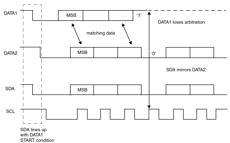
For SS-mode or FS-mode master, arbitration may continue through address, address ACK, data, and data ACK bits. Special attention must be paid, during a serial transfer, if the arbitration procedure is still in progress at the moment when a repeated START condition or a STOP condition is transmitted to the I2C bus. If it's possible for such a situation to occur, the masters involved must send this repeated START condition or STOP condition at the same position in the format frame. In other words, arbitration isn't allowed between:
A repeated START condition and a data bit
A STOP condition and a data bit
A repeated START condition and a STOP condition.
As an HS-mode master has a unique 8-bit master code, it will always finish the arbitration during the first byte (sending of HS master code). This 8-bit code is defined by the system designer and is set by writing to the IC_HS_MADDR (High Speed Master Mode Code Address) register. Because the codes are unique, only one master can win arbitration, which occurs by the end of the transmission of the high-speed master code. Control of the bus is determined by address or master code and data sent by competing masters, so there is no central master nor any order of priority on the bus.
If a master also incorporates a slave function and it loses arbitration during the addressing stage, the winning master may be trying to address it. The losing master must therefore switch over immediately to its slave mode.
Slaves are not involved in the arbitration process.
SDA/SCL Filter
The I2C provides filtering on the SDA (ic_data_in_a) and SCL (ic_scl_in_a) inputs, suppressing noise and signal spikes. Set IC_DIG_FLTR_SEL (0xEC[8]) to open the filter. Set IC_DIG_FLTR_DEG (0xEC[3:0]) to adjust the duration of noise or spikes that can be suppressed. The larger IC_DIG_FLTR_DEG is, the longer duration can be suppressed. However, the delay of signals after filter is also longer, refer to the following table.
M ─ Delay between ic_data_in_a and dig_sda or ic_scl_in_a and dig_scl is M ic_clk cycles, including 2 meta-stability removal cycles.
N ─ Noise or signal spikes with duration less than N ic_clk cycles could be suppressed.
IC_DIG_FLTR_DEG[3:1] |
N (max. filtered cycles) |
M (delay cycles) |
|---|---|---|
0 |
1 |
3 |
1 |
2 |
4 |
2 |
3 |
5 |
3 |
4 |
6 |
4 |
5 |
7 |
5 |
6 |
8 |
6 |
7 |
9 |
7 |
8 |
10 |
The I2C provides filtering on the SDA (ic_data_in_a) and SCL (ic_scl_in_a) inputs, suppressing noise and signal spikes. Set IC_DIG_FLTR_SEL (0xEC[8]) to open the filter. Set IC_DIG_FLTR_DEG (0xEC[5:0]) to adjust the duration of noise or spikes that can be suppressed. The larger IC_DIG_FLTR_DEG is, the longer duration can be suppressed. However, the delay of signals after filter is also longer, refer to the following table.
M ─ Delay between ic_data_in_a and dig_sda or ic_scl_in_a and dig_scl is M ic_clk cycles, including 2 meta-stability removal cycles.
N ─ Noise or signal spikes with duration less than N ic_clk cycles could be suppressed.
IC_DIG_FLTR_DEG[5:1] |
N (max. filtered cycles) |
M (delay cycles) |
|---|---|---|
0 |
1 |
3 |
1 |
2 |
4 |
2 |
3 |
5 |
3 |
4 |
6 |
4 |
5 |
7 |
5 |
6 |
8 |
6 |
7 |
9 |
7 |
8 |
10 |
… |
… |
… |
31 |
32 |
34 |
IC_CLK Frequency Configuration
When the I2C is configured as a master, the *CNT registers must be set before any I2C bus transaction can take place in order to ensure proper I/O timing. The *CNT registers are:
IC_SS_SCL_HCNT
IC_SS_SCL_LCNT
IC_FS_SCL_HCNT
IC_FS_SCL_LCNT
IC_HS_SCL_HCNT
IC_HS_SCL_LCNT
Note
It is not necessary to program any of the *CNT registers if the I2C is enabled to operate only as an I2C slave, since these registers are used only to determine the SCL timing requirements for operation as an I2C master.
Minimum High and Low Counts
When the I2C operates as an I2C master, in both transmit and receive transfers:
Min. value that can be programmed in the *_LCNT registers is 8.
Min. value allowed for the *_HCNT registers is 6.
The min. value of 8 for the *_LCNT registers is due to the time required for the I2C to drive SDA after a negative edge of SCL.
The min. value of 6 for the *_HCNT register is due to the time required for the I2C to sample SDA during the high period of SCL.
Programmable Duty Cycle
This section describes the minimum ic_clk frequencies that the I2C supports for each speed mode, and the associated high and low count values. Note that these limits apply to the I2C in both master and slave modes. The limits for slave mode are required so that the I2C does not break the tHD, DATmax. I2C protocol timing requirement.
High and Low Counts Calculation
The calculations below show how to calculate SCL high and low counts for each speed mode in the I2C.
The following conditions should be given:
Ic_clk frequency: \(f_{ic\_clk} \to T_{ic\_clk} = 1 / f_{ic\_clk}\)
HIGH_TIME: HIGH period of SCL
LOW_TIME: LOW period of SCL
SCL frequency: \(f_{SCL} \to SCL_{PERIOD} = 1 / f_{SCL}\)
While we want to get HIGH_COUNT & LOW_COUNT, we can derive the equations:
Then, we can get
Full Speed Mode and Standard Speed Mode Example
For I2C0, \(f_{ic\_clk} = 10\,\text{MHz}\); for I2C1/I2C2, \(f_{ic\_clk} = 100\,\text{MHz}\)
ic_clk frequency: \(f_{ic\_clk} = 10\,\text{MHz} \to T_{ic\_clk} = 100\,\text{ns}\)
According to table 5 of I2C-Bus specification version2.1, FS Mode and SS Mode timing parameters for SCL are specified as:
Standard mode: min. HIGH period of SCL is 4.0us (min. IC_SS_SCL_HCNT = 4.0us/100ns = 40)
Standard mode: min. LOW period of SCL is 4.7us (min. IC_SS_SCL_LCNT = 4.7us/100ns = 47)
Fast mode: min. HIGH period of SCL is 0.6us (min. IC_FS_SCL_HCNT = 0.6us/100ns = 6)
Fast mode: min. LOW period of SCL is 1.3us (min. IC_FS_SCL_LCNT = 1.3us/100ns = 13)
SCL frequency:
\(100\,\text{KHz} \to SCL_{PERIOD} = 10000\,\text{ns}\)
\(400\,\text{KHz} \to SCL_{PERIOD} = 2500\,\text{ns}\)
SS Mode (100KHz) :
IC_SS_SCL_HCNT = (10000ns/100ns)*(40/(40+47)) = 45.97 = 46 (round up)
IC_SS_SCL_LCNT = (10000ns/100ns)*(47/(40+47)) = 54.02 = 54 (round down)
FS Mode (400KHz):
IC_FS_SCL_HCNT = (2500ns/100ns)*(6/(6+13)) = 7.89 = 8 (round up)
IC_FS_SCL_LCNT = (2500ns/100ns)*(13/(6+13)) = 17.11 = 17 (round down)
For I2C0/I2C1, \(f_{ic\_clk} = 100\,\text{MHz}\)
ic_clk frequency: \(f_{ic\_clk} = 10\,\text{MHz} \to T_{ic\_clk} = 100\,\text{ns}\)
According to table 5 of I2C-Bus specification version2.1, FS Mode and SS Mode timing parameters for SCL are specified as:
Standard mode: min. HIGH period of SCL is 4.0us (min. IC_SS_SCL_HCNT = 4.0us/100ns = 40)
Standard mode: min. LOW period of SCL is 4.7us (min. IC_SS_SCL_LCNT = 4.7us/100ns = 47)
Fast mode: min. HIGH period of SCL is 0.6us (min. IC_FS_SCL_HCNT = 0.6us/100ns = 6)
Fast mode: min. LOW period of SCL is 1.3us (min. IC_FS_SCL_LCNT = 1.3us/100ns = 13)
SCL frequency:
\(100\,\text{KHz} \to SCL_{PERIOD} = 10000\,\text{ns}\)
\(400\,\text{KHz} \to SCL_{PERIOD} = 2500\,\text{ns}\)
SS Mode (100KHz) :
IC_SS_SCL_HCNT = (10000ns/100ns)*(40/(40+47)) = 45.97 = 46 (round up)
IC_SS_SCL_LCNT = (10000ns/100ns)*(47/(40+47)) = 54.02 = 54 (round down)
FS Mode (400KHz):
IC_FS_SCL_HCNT = (2500ns/100ns)*(6/(6+13)) = 7.89 = 8 (round up)
IC_FS_SCL_LCNT = (2500ns/100ns)*(13/(6+13)) = 17.11 = 17 (round down)
For I2C0, \(f_{ic\_clk} = 20\,\text{MHz}\); for I2C1/I2C2, \(f_{ic\_clk} = 100\,\text{MHz}\)
ic_clk frequency: \(f_{ic\_clk} = 20\,\text{MHz} \to T_{ic\_clk} = 50\,\text{ns}\)
According to table 5 of I2C-Bus specification version2.1, FS Mode and SS Mode timing parameters for SCL are specified as:
Standard mode: min. HIGH period of SCL is 4.0us (min. IC_SS_SCL_HCNT = 4.0us/50ns = 80)
Standard mode: min. LOW period of SCL is 4.7us (min. IC_SS_SCL_LCNT = 4.7us/50ns = 94)
Fast mode: min. HIGH period of SCL is 0.6us (min. IC_FS_SCL_HCNT = 0.6us/50ns = 12)
Fast mode: min. LOW period of SCL is 1.3us (min. IC_FS_SCL_LCNT = 1.3us/50ns = 26)
SCL frequency:
\(100\,\text{KHz} \to SCL_{PERIOD} = 10000\,\text{ns}\)
\(400\,\text{KHz} \to SCL_{PERIOD} = 2500\,\text{ns}\)
SS Mode (100KHz) :
IC_SS_SCL_HCNT = (10000ns/100ns)*(80/(80+94)) = 45.97 = 46 (round up)
IC_SS_SCL_LCNT = (10000ns/100ns)*(94/(80+94)) = 54.02 = 54 (round down)
FS Mode (400KHz):
IC_FS_SCL_HCNT = (2500ns/100ns)*(12/(12+26)) = 7.89 = 8 (round up)
IC_FS_SCL_LCNT = (2500ns/100ns)*(26/(12+26)) = 17.11 = 17 (round down)
For I2C0, \(f_{ic\_clk} = 10\,\text{MHz}\); for I2C1/I2C2, \(f_{ic\_clk} = 100\,\text{MHz}\)
ic_clk frequency: \(f_{ic\_clk} = 10\,\text{MHz} \to T_{ic\_clk} = 100\,\text{ns}\)
According to table 5 of I2C-Bus specification version2.1, FS Mode and SS Mode timing parameters for SCL are specified as:
Standard mode: min. HIGH period of SCL is 4.0us (min. IC_SS_SCL_HCNT = 4.0us/100ns = 40)
Standard mode: min. LOW period of SCL is 4.7us (min. IC_SS_SCL_LCNT = 4.7us/100ns = 47)
Fast mode: min. HIGH period of SCL is 0.6us (min. IC_FS_SCL_HCNT = 0.6us/100ns = 6)
Fast mode: min. LOW period of SCL is 1.3us (min. IC_FS_SCL_LCNT = 1.3us/100ns = 13)
SCL frequency:
\(100\,\text{KHz} \to SCL_{PERIOD} = 10000\,\text{ns}\)
\(400\,\text{KHz} \to SCL_{PERIOD} = 2500\,\text{ns}\)
SS Mode (100KHz) :
IC_SS_SCL_HCNT = (10000ns/100ns)*(40/(40+47)) = 45.97 = 46 (round up)
IC_SS_SCL_LCNT = (10000ns/100ns)*(47/(40+47)) = 54.02 = 54 (round down)
FS Mode (400KHz):
IC_FS_SCL_HCNT = (2500ns/100ns)*(6/(6+13)) = 7.89 = 8 (round up)
IC_FS_SCL_LCNT = (2500ns/100ns)*(13/(6+13)) = 17.11 = 17 (round down)
High Speed Mode Example
I2C0 does not support HS mode; for I2C1/2, \(f_{ic\_clk} = 100\,\text{MHz}\)
For I2C0/I2C1, \(f_{ic\_clk} = 100\,\text{MHz}\)
For I2C0/I2C1, \(f_{ic\_clk} = 100\,\text{MHz}\)
For I2C0/I2C1, \(f_{ic\_clk} = 100\,\text{MHz}\)
I2C0 does not support HS mode; for I2C1/2, \(f_{ic\_clk} = 100\,\text{MHz}\)
I2C0 does not support HS mode; for I2C1/2, \(f_{ic\_clk} = 100\,\text{MHz}\)
Ic_clk frequency: \(f_{ic\_clk} = 100\,\text{MHz} \to T_{ic\_clk} = 10\,\text{ns}\)
According to table 7 of I2C-Bus specification version2.1, HS mode timing parameters for SCL are specified as:
3.4M, bus loading=100pf: min. HIGH period of SCL is 60ns (min. IC_HS_SCL_HCNT = 60ns/10ns= 6)
3.4M, bus loading=100pf: min. LOW period of SCL is 120ns (min. IC_HS_SCL_LCNT = 120ns/10ns= 12)
1.7M, bus loading=400pf: min. HIGH period of SCL is 160ns (min. IC_HS_SCL_HCNT = 160ns/10ns= 16)
1.7M, bus loading=400pf: min. LOW period of SCL is 320ns (min. IC_HS_SCL_LCNT = 320ns/10ns= 32)
SCL frequency:
\(3.4\,\text{M} \to SCL_{PERIOD} = 294\,\text{ns}\)
\(1.7\,\text{M} \to SCL_{PERIOD} = 588\,\text{ns}\)
HS Mode (3.4M, bus loading=100pf):
IC_HS_SCL_HCNT = (294ns/10ns)*(6/(6+12)) = 9.8 = 10 (round up)
IC_HS_SCL_LCNT = (294ns/10ns)*(12/(6+12)) = 19.6 = 19 (round down)
HS Mode (1.7M, bus loading=400pf):
IC_HS_SCL_HCNT = (588ns/10ns)*(16/(16+32)) = 19.6 = 20 (round up)
IC_HS_SCL_LCNT = (588ns/10ns)*(32/(16+32)) = 39.2 = 39 (round down)
Note
Since the slave may stretch SCL line, the actual speed is a little bit smaller then 100K/400K/3.4M if we set the above calculated values. In order to reach the accurate speed, calculated values should be reduced a little according to test results.
Programmable SDA Hold Time
When I2C acts as a master transmitter:
Master ADDRESS/MSCODE phase: When the master sends addresses or master_code, the SCL from I2C bus may be inconsistent with the mst_scl from master because of the arbitration mechanism. To ensure the SDA toggles after the negative edge of SCL, shift out register is triggered by neg_scl, which is synchronization of SCL from I2C bus. The SCL to neg_scl path includes a digital filter and a two-stage synchronizer. Refer to this table, the digital filter delay of I2C bus interface is (IC_DIG_FLTR_DEG[3:1] +3) cycles.
The hold time is maximum of (5+ IC_DIG_FLTR_DEG[3:1]) and IC_SDA_HOLD.
Master WDATA phase: the mst_SCL is synchronized with the SCL of the I2C bus, use negedge of mst_SCL to trigger shift out register.
The hold time is IC_SDA_HOLD ic_clk periods.
When I2C acts as a slave transmitter:
Slave WDATA phase: Shift out register is triggered by neg_scl, which is synchronization of SCL from I2C bus. The SCL to neg_scl path includes a digital filter and a two-stage synchronizer. Refer to this table, the digital filter delay of I2C bus interface is (IC_DIG_FLTR_DEG[3:1] +3) cycles.
The hold time is maximum of (5+ IC_DIG_FLTR_DEG[3:1]) and IC_SDA_HOLD.
When I2C acts as a master transmitter:
Master ADDRESS/MSCODE phase: When the master sends addresses or master_code, the SCL from I2C bus may be inconsistent with the mst_scl from master because of the arbitration mechanism. To ensure the SDA toggles after the negative edge of SCL, shift out register is triggered by neg_scl, which is synchronization of SCL from I2C bus. The SCL to neg_scl path includes a digital filter and a two-stage synchronizer. Refer to this table, the digital filter delay of I2C bus interface is (IC_DIG_FLTR_DEG[5:1] +3) cycles.
The hold time is maximum of (5+ IC_DIG_FLTR_DEG[5:1]) and IC_SDA_HOLD.
Master WDATA phase: the mst_SCL is synchronized with the SCL of the I2C bus, use negedge of mst_SCL to trigger shift out register.
The hold time is IC_SDA_HOLD ic_clk periods.
When I2C acts as a slave transmitter:
Slave WDATA phase: Shift out register is triggered by neg_scl, which is synchronization of SCL from I2C bus. The SCL to neg_scl path includes a digital filter and a two-stage synchronizer. Refer to this table, the digital filter delay of I2C bus interface is (IC_DIG_FLTR_DEG[5:1] +3) cycles.
The hold time is maximum of (5+ IC_DIG_FLTR_DEG[5:1]) and IC_SDA_HOLD.
Note
The 8th bit of data is not under control of IC_SDA_HOLD, because after the 8th SCL clock negative edge, receiver controls the SDA line to respond ACK or NACK.
The IC_SDA_HOLD register can be programmed only when I2C is disabled (IC_ENABLE =0).
Slave Mode Dual Own Address
The I2C has dual own address:
Slave 1 supports 7-bit or 10-bit address modes.
Slave 2 only supports 7-bit address mode.
Set IC_CON [7:6] (
0x10) to enable slave 1 or slave 2.Slave 1 address is set in IC_SAR (
0x08), which supports 7 bits or 10 bits.Slave 2 address is set in IC_SAR2 (
0xF4), which only supports 7 bits.IC_CON [3] (
0x10) IC_10BITADDR_SLAVE controls whether the I2C responds to 7-bit or 10-bit address.If slave 1 and slave 2 are both enabled, the one who matches address would response ACK.
Operation Flow
This section provides information on operation modes.
Note
The I2C should only be set to operate as an I2C master, or I2C slave, but not both simultaneously. This is achieved by ensuring that bit[6] (IC_SLAVE_DISABLE) and bit[0] (MASTER_MODE) of the IC_CON register are never set to 0 and 1 respectively.
Slave Mode Operation
This section discusses slave mode procedures.
Initial Configuration
To use the I2C as a slave, perform the following steps:
Disable the I2C by writing a ‘0’ to bit[0] of the IC_ENABLE register.
Write the IC_SAR register (bit[9:0]) to set the slave address. This is the address to which the I2C responds.
Write the IC_CON register to specify which type of addressing is supported (7-bit or 10-bit by setting bit[3]). Enable the I2C in slave-only mode by writing a ‘0’ into bit[6] (IC_SLAVE_DISABLE) and a ‘0’ to bit[0] (MASTER_MODE).
Enable the I2C by writing a ‘1’ in bit[0] of the IC_ENABLE register.
Note
The slaves and masters do not have to be programmed with the same type of addressing 7-bit or 10-bit address. For instance, a slave can be programmed with 7-bit addressing and a master with 10-bit addressing, and vice versa.
The I2C initialization configuration in slave mode is illustrated below.

Slave-Transmitter Operation for a Single Byte
When another I2C master device on the bus addresses the I2C and requests data, the I2C acts as a slave-transmitter and the following steps occur:
The other I2C master device initiates an I2C transfer with an address that matches the slave address in the IC_SAR register of the I2C.
The I2C acknowledges the sent address and recognizes the direction of the transfer to indicate that it is acting as a slave-transmitter.
The I2C asserts the RD_REQ interrupt (bit[5] of the IC_RAW_INTR_STAT register) and holds the SCL line low. It is in a wait state until software responds.
Reads that indicate IC_RAW_INTR_STAT [5] (R_RD_REQ bit) being set to 1 must be treated as the equivalent of the RD_REQ interrupt being asserted.
Software must then act to satisfy the I2C transfer.
If there is any data remaining in the Tx FIFO before receiving the read request, then the I2C asserts a TX_ABRT interrupt (bit[6] of the IC_RAW_INTR_STAT register) to flush the old data from the Tx FIFO.
Note
Because the I2C’s Tx FIFO is forced into a flushed/reset state whenever a TX_ABRT Interrupt clear event occurs, it is necessary for software to release the I2C from this state by reading the IC_CLR_TX_ABRT register before attempting to write into the Tx FIFO. See register IC_RAW_INTR_STAT for more details.
Reads that indicate bit[6] (R_TX_ABRT) being set to 1 must be treated as the equivalent of the TX_ABRT interrupt being asserted.
There is no further action required from software.
Software writes to the IC_DATA_CMD register with the data to be written (by writing a ‘0’ in bit[8]).
Software must clear the RD_REQ and TX_ABRT interrupts (bit[5] and bit[6] respectively) of the IC_RAW_INTR_STAT register before proceeding.
The I2C releases the SCL and transmits the byte.
The master may hold the I2C bus by issuing a RESTART condition or release the bus by issuing a STOP condition.
The I2C data transmission in slave mode is illustrated below.

Slave-Receiver Operation for a Single Byte
When another I2C master device on the bus addresses the I2C and is sending data, the I2C acts as a slave-receiver and the following steps occur:
The other I2C master device initiates an I2C transfer with an address that matches the I2C’s slave address in the IC_SAR register.
The I2C acknowledges the sent address and recognizes the direction of the transfer to indicate that the I2C is acting as a slave-receiver.
I2C receives the transmitted byte and places it in the receive buffer.
Note
If the Rx FIFO is completely filled with data when a byte is pushed, then an overflow occurs and the I2C continues with subsequent I2C transfers. Because a NACK is not generated, software must recognize the overflow when indicated by the I2C (by the R_RX_OVER bit in the IC_INTR_STAT register) and take appropriate actions to recover from lost data. Hence, there is a real time constraint on software to service the Rx FIFO before the latter overflow as there is no way to reapply pressure to the remote transmitting master. You must select a deep enough Rx FIFO depth to satisfy the interrupt service interval of their system.
I2C asserts the RX_FULL interrupt (IC_RAW_INTR_STAT [2] register).
If the RX_FULL interrupt has been masked, due to setting IC_INTR_MASK [2] register to 0 or setting IC_TX_TL to a value larger than 0, then it is recommended that a timing routine be implemented for periodic reads of the IC_STATUS register. Reads of the IC_STATUS register, with bit[3] (RFNE) set at 1, must then be treated by software as the equivalent of the RX_FULL interrupt being asserted.
Software may read the byte from the IC_DATA_CMD register (bit[7:0]).
The other master device may hold the I2C bus by issuing a RESTART condition or release the bus by issuing a STOP condition.
The I2C data reception in slave mode is illustrated below.

Slave-Transfer Operation for Bulk Transfers
In the standard I2C protocol, all transactions are single byte transactions and the programmer responds to a remote master read request by writing one byte into the slave’s Tx FIFO. When a slave (slave-transmitter) is issued with a read request (RD_REQ) from the remote master (master-receiver), at a minimum there should be at least one entry placed into the slave-transmitter’s Tx FIFO. I2C is designed to handle more data in the Tx FIFO so that subsequent read requests can take that data without raising an interrupt to get more data. Ultimately, this eliminates the possibility of significant latencies being incurred between raising the interrupt for data each time had there been a restriction of having only one entry placed in the Tx FIFO.
This mode only occurs when I2C is acting as a slave-transmitter. If the remote master acknowledges the data sent by the slave-transmitter and there is no data in the slave’s Tx FIFO, the I2C holds the I2C SCL line low while it raises the read request interrupt (RD_REQ) and waits for data to be written into the Tx FIFO before it can be sent to the remote master.
If the RD_REQ interrupt is masked, due to bit[5] (M_RD_REQ) of the IC_INTR_STAT register being set to 0, then it is recommended that a timing routine be used to activate periodic reads of the IC_RAW_INTR_STAT register. Reads of IC_RAW_INTR_STAT that return bit[5] (R_RD_REQ) set to 1 must be treated as the equivalent of the RD_REQ interrupt referred to in this section.
The RD_REQ interrupt is raised upon a read request, and like interrupts, must be cleared when exiting the interrupt service handling routine (ISR). The ISR allows you to either write 1 byte or more than 1 byte into the Tx FIFO. During the transmission of these bytes to the master, if the master acknowledges the last byte, then the slave must raise the RD_REQ again because the master is requesting for more data.
If the programmer knows in advance that the remote master is requesting a packet of n bytes, then when another master addresses I2C and requests data, the Tx FIFO could be written with n number bytes and the remote master receives it as a continuous stream of data. For example, the I2C slave continues to send data to the remote master as long as the remote master is acknowledging the data sent and there is data available in the Tx FIFO. There is no need to hold the SCL line low or to issue RD_REQ again.
If the remote master is to receive n bytes from the I2C but the programmer wrote a number of bytes larger than n to the Tx FIFO, then when the slave finishes sending the requested n bytes, it clears the Tx FIFO and ignores any excess bytes.
Master Mode Operation
This section discusses master mode procedures.
Initial Configuration
The target address and address format can be changed dynamically without having to disable I2C. This parameter only applies to when I2C is acting as a master because the slave requires the component to be disabled before any changes can be made to the address.
The procedures are very similar and are only different with regard to where the IC_10BITADDR_MASTER bit is set (bit[12] of IC_TAR register).
Disable the I2C by writing 0 to the IC_ENABLE register.
Write to the IC_CON register to set the maximum speed mode supported for slave operation (bit[2:1]). Writing 1 to bit[0] and bit[6] to enable Master Module and disable Slave Module.
Write to the IC_TAR register the address of the I2C device to be addressed. It also indicates whether a General Call or a START BYTE command is going to be performed by I2C. The desired speed of the I2C master-initiated transfers, either 7-bit or 10-bit addressing, is controlled by the IC_10BITADDR_MASTER bit (bit[12]).
Enable the I2C by writing a ‘1’ in the IC_ENABLE register.
Write transfer direction and data to be sent to the IC_DATA_CMD register. If the IC_DATA_CMD register is written before the I2C is enabled, the data and commands are lost as the buffers are kept cleared when I2C is disabled.
The I2C initialization configuration in master mode is illustrated below.

Dynamic IC_TAR or IC_10BITADDR_MASTER Update
The I2C supports dynamic updating of the IC_TAR (bit[9:0]) and IC_10BITADDR_MASTER (bit[12]) bits of the IC_TAR register. You can dynamically write to the IC_TAR register provided the following conditions are met:
I2C is not enabled (IC_ENABLE =0); OR
I2C is enabled (IC_ENABLE =1); AND
I2C is NOT engaged in any Master (tx, rx) operation (IC_STATUS [5]=0); AND
I2C is enabled to operate in Master mode (IC_CON [0]=1); AND
There are NO entries in the Tx FIFO (IC_STATUS [2]=1)
Master Transmit and Master Receive
To transmit data, write the data to be written to the lower byte of the I2C Rx/Tx Data Buffer and Command Register (IC_DATA_CMD). The bit[8] (CMD) should be written to 0 for I2C write operations. Subsequently, a read command may be issued by writing “don’t cares” to the lower byte of the IC_DATA_CMD register, and a 1 should be written to the CMD bit. The I2C master continues to initiate transfers as long as there are commands present in the transmit FIFO. If the STOP bit set 1, the I2C inserts a STOP condition after completing the current transfer.
The I2C supports switching back and forth between reading and writing dynamically. For combine transfer, a 1 should be write to the RESTART bit of the last command ahead of reverse direction.
Registers
This section describes the programmable registers of the I2C.
Name |
Address offset |
Access |
Description |
|---|---|---|---|
000h |
R/W |
||
004h |
R/W |
||
008h |
R/W |
||
00Ch |
R/W |
||
010h |
R/W |
||
014h |
R/W |
||
018h |
R/W |
||
01Ch |
R/W |
||
020h |
R/W |
||
024h |
R/W |
||
028h |
R/W |
||
02Ch |
R |
||
030h |
R/W |
||
034h |
R |
||
038h |
R/W |
||
03Ch |
R/W |
||
040h |
R |
||
044h |
R |
||
048h |
R |
||
04Ch |
R |
||
050h |
R |
||
054h |
R |
||
058h |
R |
||
05Ch |
R |
||
060h |
R |
||
064h |
R |
||
068h |
R |
||
06Ch |
R/W |
||
070h |
R |
||
074h |
R |
||
078h |
R |
||
07Ch |
R/W |
||
080h |
R |
||
084h |
R/W |
||
088h |
R/W |
||
08Ch |
R/W |
||
090h |
R/W |
||
094h |
R/W |
||
098h |
R/W |
||
09Ch |
R |
||
0A0h |
R/W |
||
0A4h |
R/W |
||
0A8h |
R/W |
||
0ACh |
R |
||
0B0h |
R/W |
||
0B4h |
R/W |
||
0E4h |
R |
||
0E8h |
R |
||
0ECh |
R/W |
||
0F4h |
R/W |
||
0FCh |
R |
||
100h |
R |
REG_IC_CON
Name : I2C Control Register
Size : 32
Address offset : 000h
Read/write access : R/W
Bit |
Symbol |
Access |
Reset |
Description |
|---|---|---|---|---|
31:8 |
RSVD |
R |
- |
Reserved |
7 |
IC_SLAVE_DISABLE_1 |
R/W |
0x0 |
This bit controls whether I2C has its slave2 (7-bit address ) disabled.
|
6 |
IC_SLAVE_DISABLE_0 |
R/W |
0x0 |
This bit controls whether I2C has its slave1 (7-bit or 10- bit address) disabled.
|
5 |
IC_RESTATRT_EN |
R/W |
0x0 |
Determine whether RESTART conditions may be sent when acting as a master.
|
4 |
RSVD |
R |
- |
Reserved |
3 |
IC_10BITADDR_SLAVE |
R/W |
0x0 |
When acting as a slave, this bit controls whether the I2C re sponds to 7- or 10-bit addresses.
|
2:1 |
SPEED |
R/W |
0x0 |
These bits control at which speed the I2C operates; its sett ing is relevant only if one is operating the I2C in master m ode.
|
0 |
MASTER_MODE |
R/W |
0x0 |
This bit controls whether the I2C master is enabled.
|
REG_IC_TAR
Name : I2C Target Address Register
Size : 32
Address offset : 004h
Read/write access : R/W
Bit |
Symbol |
Access |
Reset |
Description |
|---|---|---|---|---|
31:13 |
RSVD |
R |
- |
Reserved |
12 |
IC_10BITADDR_MASTER |
R/W |
0x0 |
Control whether I2C starts its transfers in 7- or 10-bit a ddressing mode when acting as a master.
|
11 |
SPECIAL |
R/W |
0x0 |
This bit indicates whether software performs a General Call or START BYTE command.
|
10 |
GC_OR_START |
R/W |
0x0 |
If SPECIAL is set to 1, then this bit indicates whether a Ge neral Call or START BYTE command is to be performed by I2C. (ic_clk domain)
|
9:0 |
IC_TAR |
R/W |
0x10 |
This is the target address for any master transaction. When transmitting a General Call, these bits are ignored. To gene rate a START BYTE, the CPU needs to write only once into the se bits. |
REG_IC_SAR
Name : I2C Slave Address Register
Size : 32
Address offset : 008h
Read/write access : R/W
Bit |
Symbol |
Access |
Reset |
Description |
|---|---|---|---|---|
31:10 |
RSVD |
R |
- |
Reserved |
9:0 |
IC_SAR |
R/W |
0x11 |
The IC_SAR holds the slave address when the I2C is operating as slave1. For 7-bit addressing, only IC_SAR[6:0] is used. The register can be written only when the I2C interface is d isabled, which corresponds to the IC_ENABLE register being s et to 0. Writes at other times have no effect. |
REG_IC_HS_MAR
Name : I2C High Speed Master Mode Code Address Register
Size : 32
Address offset : 00Ch
Read/write access : R/W
Bit |
Symbol |
Access |
Reset |
Description |
|---|---|---|---|---|
31:3 |
RSVD |
R |
- |
Reserved |
2:0 |
IC_HS_MAR |
R/W |
0x0 |
This bit field holds the value of the I2C HS mode master cod e. HS-mode master codes are reserved 8-bit codes (00001xxx ) that are not used for slave addressing or other purposes. This register can be written only when the I2C interface is disabled, which corresponds to the IC_ENABLE register being set to 0. Write at other times have no effect. |
REG_IC_DATA_CMD
Name : I2C Rx/Tx Data Buffer and Command Register
Size : 32
Address offset : 010h
Read/write access : R/W
Bit |
Symbol |
Access |
Reset |
Description |
|---|---|---|---|---|
31:12 |
RSVD |
R |
- |
Reserved |
11 |
NULL_DATA |
R/W |
0x0 |
|
10 |
CMD_RESTART |
R/W |
0x0 |
This bit controls whether a RESTART is issued after the byte is sent or received.
|
9 |
CMD_STOP |
R/W |
0x0 |
This bit controls whether a STOP is issued after the byte is sent or received.
|
8 |
CMD_RW |
R/W |
0x0 |
This bit controls whether a read or write is performed. This bit does not control the direction when the I2C acts as a sl ave. It controls only the direction when it acts as a master .
|
7:0 |
IC_DATA |
R/W |
0x0 |
This register contains the data to be transmitted or receive d on the I2C bus. If you are writing to this register and wa nt to perform a read, these bits are ignored by the I2C. How ever, when you read this register, these bits return the val ue of data received on the I2C interface. |
REG_IC_SS_SCL_HCNT
Name : Standard Speed I2C Clock SCL High Count Register
Size : 32
Address offset : 014h
Read/write access : R/W
Bit |
Symbol |
Access |
Reset |
Description |
|---|---|---|---|---|
31:16 |
RSVD |
R |
- |
Reserved |
15:0 |
IC_SS_SCL_HCNT |
R/W |
0x0190 |
This register sets the SCL clock high-period count for stan dard speed. This register must be set before any I2C bus transaction can take place to ensure proper I/O timing. This register can be written only when the I2C interface is disabled which corresponds to the IC_ENABLE register being s et to 0. Writes at other times have no effect. |
REG_IC_SS_SCL_LCNT
Name : Standard Speed I2C Clock SCL Low Count Register
Size : 32
Address offset : 018h
Read/write access : R/W
Bit |
Symbol |
Access |
Reset |
Description |
|---|---|---|---|---|
31:16 |
RSVD |
R |
- |
Reserved |
15:0 |
IC_SS_SCL_LCNT |
R/W |
0x01D6 |
This register sets the SCL clock low-period count for stand ard speed. This register must be set before any I2C bus transaction can take place to ensure proper I/O timing. This register can be written only when the I2C interface is disabled which corresponds to the IC_ENABLE register being s et to 0. Writes at other times have no effect. |
REG_IC_FS_SCL_HCNT
Name : Fast Speed I2C Clock SCL High Count Register
Size : 32
Address offset : 01Ch
Read/write access : R/W
Bit |
Symbol |
Access |
Reset |
Description |
|---|---|---|---|---|
31:16 |
RSVD |
R |
- |
Reserved |
15:0 |
IC_FS_SCL_HCNT |
R/W |
0x003C |
This register sets the SCL clock high-period count for fast speed. This register must be set before any I2C bus transaction can take place to ensure proper I/O timing. This register can be written only when the I2C interface is disabled which corresponds to the IC_ENABLE register being s et to 0. Writes at other times have no effect. |
REG_IC_FS_SCL_LCNT
Name : Fast Speed I2C Clock SCL Low Count Register
Size : 32
Address offset : 020h
Read/write access : R/W
Bit |
Symbol |
Access |
Reset |
Description |
|---|---|---|---|---|
31:16 |
RSVD |
R |
- |
Reserved |
15:0 |
IC_FS_SCL_LCNT |
R/W |
0x0082 |
This register sets the SCL clock low-period count for fast speed. This register must be set before any I2C bus transaction can take place to ensure proper I/O timing. This register can be written only when the I2C interface is disabled which corresponds to the IC_ENABLE register being s et to 0. Writes at other times have no effect. |
REG_IC_HS_SCL_HCNT
Name : High Speed I2C Clock SCL High Count Register
Size : 32
Address offset : 024h
Read/write access : R/W
Bit |
Symbol |
Access |
Reset |
Description |
|---|---|---|---|---|
31:16 |
RSVD |
R |
- |
Reserved |
15:0 |
IC_HS_SCL_HCNT |
R/W |
0x0006 |
This register sets the SCL clock high-period count for high speed. This register must be set before any I2C bus transaction can take place to ensure proper I/O timing. This register can be written only when the I2C interface is disabled which corresponds to the IC_ENABLE register being s et to 0. Writes at other times have no effect. The SCL High time depends on the loading of the bus. For 100 pF loading, the SCL High time is 60ns; for 400pF loading, th e SCL High time is 120ns. |
REG_IC_HS_SCL_LCNT
Name : High Speed I2C Clock SCL Low Count Register
Size : 32
Address offset : 028h
Read/write access : R/W
Bit |
Symbol |
Access |
Reset |
Description |
|---|---|---|---|---|
31:16 |
RSVD |
R |
- |
Reserved |
15:0 |
IC_HS_SCL_LCNT |
R/W |
0x0010 |
This register sets the SCL clock low-period count for high speed. This register must be set before any I2C bus transaction can take place to ensure proper I/O timing. This register can be written only when the I2C interface is disabled which corresponds to the IC_ENABLE register being s et to 0. Writes at other times have no effect. The SCL Low time depends on the loading of the bus. For 100p F loading, the SCL High time is 160ns; for 400pF loading, th e SCL High time is 320ns. |
REG_IC_INTR_STAT
Name : I2C Interrupt Status Register
Size : 32
Address offset : 02Ch
Read/write access : R
Bit |
Symbol |
Access |
Reset |
Description |
|---|---|---|---|---|
31:14 |
RSVD |
R |
- |
Reserved |
13 |
R_LP_WAKE_2 |
R |
0x0 |
|
12 |
R_LP_WAKE_1 |
R |
0x0 |
|
11 |
R_GEN_CALL |
R |
0x0 |
|
10 |
R_START_DET |
R |
0x0 |
|
9 |
R_STOP_DET |
R |
0x0 |
|
8 |
R_ACTIVITY |
R |
0x0 |
|
7 |
R_RX_DONE |
R |
0x0 |
|
6 |
R_TX_ABRT |
R |
0x0 |
|
5 |
R_RD_REQ |
R |
0x0 |
|
4 |
R_TX_EMPTY |
R |
0x0 |
|
3 |
R_TX_OVER |
R |
0x0 |
|
2 |
R_RX_FULL |
R |
0x0 |
|
1 |
R_RX_OVER |
R |
0x0 |
|
0 |
R_RX_UNDER |
R |
0x0 |
REG_IC_INTR_MASK
Name : I2C Interrupt Mask Register
Size : 32
Address offset : 030h
Read/write access : R/W
Bit |
Symbol |
Access |
Reset |
Description |
|---|---|---|---|---|
31:14 |
RSVD |
R |
- |
Reserved |
13 |
M_LP_WAKE_2 |
R/W |
0x0 |
|
12 |
M_LP_WAKE_1 |
R/W |
0x0 |
|
11 |
M_GEN_CALL |
R/W |
0x0 |
|
10 |
M_START_DET |
R/W |
0x0 |
|
9 |
M_STOP_DET |
R/W |
0x0 |
|
8 |
M_ACTIVITY |
R/W |
0x0 |
|
7 |
M_RX_DONE |
R/W |
0x0 |
|
6 |
M_TX_ABRT |
R/W |
0x0 |
|
5 |
M_RD_REQ |
R/W |
0x0 |
|
4 |
M_TX_EMPTY |
R/W |
0x0 |
|
3 |
M_TX_OVER |
R/W |
0x0 |
|
2 |
M_RX_FULL |
R/W |
0x0 |
|
1 |
M_RX_OVER |
R/W |
0x0 |
|
0 |
M_RX_UNDER |
R/W |
0x0 |
REG_IC_RAW_INTR_STAT
Name : I2C Raw Interrupt Status Register
Size : 32
Address offset : 034h
Read/write access : R
Bit |
Symbol |
Access |
Reset |
Description |
|---|---|---|---|---|
31:14 |
RSVD |
R |
- |
Reserved |
13 |
LP_WAKE_2 |
R |
0x0 |
Set when address SAR_2 match with address sending on I2C BU S. |
12 |
LP_WAKE_1 |
R |
0x0 |
Set when address SAR match with address sending on I2C BUS. |
11 |
GEN_CALL |
R |
0x0 |
Set only when a General Call address is received and it is a cknowledged. |
10 |
START_DET |
R |
0x0 |
Indicates whether a START or RESTART condition has occurred on the I2C interface regardless of whether I2C is operating in slave or master mode. |
9 |
STOP_DET |
R |
0x0 |
Indicates whether a STOP condition has occurred on the I2C i nterface regardless of whether I2C is operating in slave or master mode. |
8 |
ACTIVITY |
R |
0x0 |
This bit captures I2C activity. |
7 |
RX_DONE |
R |
0x0 |
When the I2C is acting as a slave-transmitter, this bit is set to 1 if the master does not acknowledge a transmitted by te. This occurs on the last byte of the transmission, indica ting that the transmission is done. |
6 |
TX_ABRT |
R |
0x0 |
This bit indicates if I2C as a transmitter, is unable to com plete the intended actions on the contents of the transmit F IFO. This situation can occur both as an I2C master or an I2 C slave, and is referred to as a ‘transmit abort’.
|
5 |
RD_REQ |
R |
0x0 |
This bit is set to 1 when I2C is acting as a slave and anoth er I2C master is attempting to read data from I2C. The I2C h olds the I2C bus in a wait state(SCL=0) until this interrupt is serviced, which means that the slave has been addressed b y a remote master that is asking for data to be transferred. The processor must respond to this interrupt and then write the requested data to the IC_DATA_CMD register. |
4 |
TX_EMPTY |
R |
0x0 |
This bit is set to 1 when the transmit buffer is at or below the threshold value set in the IC_TX_TL register. It is auto matically cleared by hardware when the buffer level goes abo ve the threshold. |
3 |
TX_OVER |
R |
0x0 |
Set during transmit if the transmit buffer is filled to IC_T X_BUFFER_DEPTH and the processor attempts to issue another I 2C command by writing to the IC_DATA_CMD register. |
2 |
RX_FULL |
R |
0x0 |
Set when the receive buffer goes above the RX_TL threshold i n the IC_RX_TL register. It is automatically cleared by hard ware when buffer level is equal to or less than the threshol d. |
1 |
RX_OVER |
R |
0x0 |
Not used. Set if the receive buffer is completely filled to IC_RX_BUFFER_DEPTH and an additional byte is received from a n external I2C device. |
0 |
RX_UNDER |
R |
0x0 |
Set if the processor attempts to read the receive buffer whe n it is empty by reading from the IC_DATA_CMD register. |
REG_IC_RX_TL
Name : I2C Receive FIFO Threshold Register
Size : 32
Address offset : 038h
Read/write access : R/W
Bit |
Symbol |
Access |
Reset |
Description |
|---|---|---|---|---|
31:8 |
RSVD |
R |
- |
Reserved |
7:0 |
IC_RX_0_TL |
R/W |
0x0 |
Receive FIFO Threshold Level. Control the level of entries (or above) that triggers the RX _FULL interrupt (bit 2 in IC_RAW_INTR_STAT register). |
REG_IC_TX_TL
Name : I2C Transmit FIFO Threshold Register
Size : 32
Address offset : 03Ch
Read/write access : R/W
Bit |
Symbol |
Access |
Reset |
Description |
|---|---|---|---|---|
31:8 |
RSVD |
R |
- |
Reserved |
7:0 |
IC_TX_0_TL |
R/W |
0x0 |
Transmit FIFO Threshold Level. Control the level of entries (or below) that triggers the TX _EMPTY interrupt (bit 4 in IC_RAW_INTR_STAT register). |
REG_IC_CLR_INTR
Name : Clear Combined and Individual Interrupt Register
Size : 32
Address offset : 040h
Read/write access : R
Bit |
Symbol |
Access |
Reset |
Description |
|---|---|---|---|---|
31:1 |
RSVD |
R |
- |
Reserved |
0 |
CLR_INRT |
R |
0x0 |
Read this register to clear the combined interrupt, all indi vidual interrupts, and the IC_TX_ABRT_SOURCE register. This bit does not clear hardware clearable interrupts but softwar e clearable interrupts. |
REG_IC_CLR_RX_UNDER
Name : Clear RX_UNDER Interrupt Register
Size : 32
Address offset : 044h
Read/write access : R
Bit |
Symbol |
Access |
Reset |
Description |
|---|---|---|---|---|
31:1 |
RSVD |
R |
- |
Reserved |
0 |
CLR_RX_UNDER |
R |
0x0 |
Read this register to clear the RX_UNDER interrupt (bit 0) o f IC_RAW_INTR_STAT register. |
REG_IC_CLR_RX_OVER
Name : Clear RX_OVER Interrupt Register
Size : 32
Address offset : 048h
Read/write access : R
Bit |
Symbol |
Access |
Reset |
Description |
|---|---|---|---|---|
31:1 |
RSVD |
R |
- |
Reserved |
0 |
CLR_RX_OVER |
R |
0x0 |
Read this register to clear the RX_OVER interrupt (bit 1) of IC_RAW_INTR_STAT register. |
REG_IC_CLR_TX_OVER
Name : Clear TX_OVER Interrupt Register
Size : 32
Address offset : 04Ch
Read/write access : R
Bit |
Symbol |
Access |
Reset |
Description |
|---|---|---|---|---|
31:1 |
RSVD |
R |
- |
Reserved |
0 |
CLR_TX_OVER |
R |
0x0 |
Read this register to clear the TX_OVER interrupt (bit 3) of IC_RAW_INTR_STAT register. |
REG_IC_CLR_RD_REQ
Name : Clear RD_REQ Interrupt Register
Size : 32
Address offset : 050h
Read/write access : R
Bit |
Symbol |
Access |
Reset |
Description |
|---|---|---|---|---|
31:1 |
RSVD |
R |
- |
Reserved |
0 |
CLR_RD_REQ |
R |
0x0 |
Read this register to clear the RD_REQ interrupt (bit 5) of IC_RAW_INTR_STAT register. |
REG_IC_CLR_TX_ABRT
Name : Clear TX_ABRT Interrupt Register
Size : 32
Address offset : 054h
Read/write access : R
Bit |
Symbol |
Access |
Reset |
Description |
|---|---|---|---|---|
31:1 |
RSVD |
R |
- |
Reserved |
0 |
CLR_TX_ABRT |
R |
0x0 |
Read this register to clear the TX_ABRT interrupt (bit 6) of IC_RAW_INTR_STAT register, and the IC_TX_ABRT_SOURCE registe r. This is also releases the TX FIFO from the flushed/reset state, allowing more writes to the TX FIFO. |
REG_IC_CLR_RX_DONE
Name : Clear RX_DONE Interrupt Register
Size : 32
Address offset : 058h
Read/write access : R
Bit |
Symbol |
Access |
Reset |
Description |
|---|---|---|---|---|
31:1 |
RSVD |
R |
- |
Reserved |
0 |
CLR_RX_DONE |
R |
0x0 |
Read this register to clear the RX_DONE interrupt (bit 7) of IC_RAW_INTR_STAT register. |
REG_IC_CLR_ACTIVITY
Name : Clear ACTIVITY Interrupt Register
Size : 32
Address offset : 05Ch
Read/write access : R
Bit |
Symbol |
Access |
Reset |
Description |
|---|---|---|---|---|
31:1 |
RSVD |
R |
- |
Reserved |
0 |
CLR_ACTIVITY |
R |
0x0 |
Read this register to clear the ACTIVITY interrupt if the I2 C is not active anymore. If the I2C module is still active o n the bus, the ACTIVITY interrupt bit continues to be set. I t is automatically cleared by hardware if the module is disa bled and if there is no further activity on the bus. The val ue read from this register to get status of the ACTIVITY int errupt (bit 8) of the IC_RAW_INTR_STAT register. |
REG_IC_CLR_STOP_DET
Name : Clear STOP_DET Interrupt Register
Size : 32
Address offset : 060h
Read/write access : R
Bit |
Symbol |
Access |
Reset |
Description |
|---|---|---|---|---|
31:1 |
RSVD |
R |
- |
Reserved |
0 |
CLR_STOP_DET |
R |
0x0 |
Ead this register to clear the STOP_DET interrupt (bit 9) of IC_RAW_INTR_STAT register. |
REG_IC_CLR_START_DET
Name : Clear START_DET Interrupt Register
Size : 32
Address offset : 064h
Read/write access : R
Bit |
Symbol |
Access |
Reset |
Description |
|---|---|---|---|---|
31:1 |
RSVD |
R |
- |
Reserved |
0 |
CLR_START_DET |
R |
0x0 |
Ead this register to clear the START_DET interrupt (bit 10) of IC_RAW_INTR_STAT register. |
REG_IC_CLR_GEN_CALL
Name : Clear GEN_ALL Interrupt Register
Size : 32
Address offset : 068h
Read/write access : R
Bit |
Symbol |
Access |
Reset |
Description |
|---|---|---|---|---|
31:1 |
RSVD |
R |
- |
Reserved |
0 |
CLR_GEN_CALL |
R |
0x0 |
Ead this register to clear the GEN_CALL interrupt (bit 11) o f IC_RAW_INTR_STAT register. |
REG_IC_ENABLE
Name : I2C Enable Register
Size : 32
Address offset : 06Ch
Read/write access : R/W
Bit |
Symbol |
Access |
Reset |
Description |
|---|---|---|---|---|
31:2 |
RSVD |
R |
- |
Reserved |
1 |
FORCE |
R/W |
0x0 |
Force master I2C stop transfer immediately after IC_ENABLE s et 0.
|
0 |
ENABLE |
R/W |
0x0 |
Control whether the I2C is enabled.
|
REG_IC_STATUS
Name : I2C Status Register
Size : 32
Address offset : 070h
Read/write access : R
Bit |
Symbol |
Access |
Reset |
Description |
|---|---|---|---|---|
31:10 |
RSVD |
R |
- |
Reserved |
9:8 |
BUS_MONITOR_STATUS |
R |
0x0 |
BUS monitor status:
|
7 |
RSVD |
R |
- |
Reserved |
6 |
SLV_ACTIVITY |
R |
0x0 |
Slave FSM Activity Status. When the Slave FSM is not in the IDLE state, this bit is set.
|
5 |
MST_ACTIVITY |
R |
0x0 |
Master FSM Activity Status. When the Master FSM is not in th e IDLE state, this bit is set.
|
4 |
RFF |
R |
0x0 |
Receive FIFO Completely Full. When the receive FIFO is compl etely full, this bit is set. When the receive FIFO contains one or more empty location, this bit is cleared.
|
3 |
RFNE |
R |
0x0 |
Receive FIFO Not Empty. This bit is set when the receive FIF O contains one or more entries; it is cleared when the recei ve FIFO is empty.
|
2 |
TFE |
R |
0x1 |
Transmit FIFO Completely Empty. When the transmit FIFO is co mpletely empty, this bit is set. When it contains one or mor e valid entries, this bit is cleared. This bit field does no t request an interrupt.
|
1 |
TFNF |
R |
0x1 |
Transmit FIFO Not Full. Set when the transmit FIFO contains one or more empty locations, and is cleared when the FIFO is full.
|
0 |
IC_ACTIVITY |
R |
0x0 |
I2C Activity Status. |
REG_IC_TXFLR
Name : I2C Transmit FIFO Level Register
Size : 32
Address offset : 074h
Read/write access : R
Bit |
Symbol |
Access |
Reset |
Description |
|---|---|---|---|---|
31:6 |
RSVD |
R |
- |
Reserved |
5:0 |
TXFLR |
R |
0x0 |
Transmit FIFO Level. Contains the number of valid data entri es in the transmit FIFO. |
REG_IC_RXFLR
Name : I2C Receive FIFO Level Register
Size : 32
Address offset : 078h
Read/write access : R
Bit |
Symbol |
Access |
Reset |
Description |
|---|---|---|---|---|
31:6 |
RSVD |
R |
- |
Reserved |
5:0 |
RXFLR |
R |
0x0 |
Receive FIFO Level. Contains the number of valid data entrie s in the receive FIFO. |
REG_IC_SDA_HOLD
Name : I2C SDA Hold Time Length Register
Size : 32
Address offset : 07Ch
Read/write access : R/W
Bit |
Symbol |
Access |
Reset |
Description |
|---|---|---|---|---|
31:16 |
RSVD |
R |
- |
Reserved |
15:0 |
IC_SDA_HOLD |
R/W |
0x1 |
Set the required SDA hold time in units of ic_clk period. |
REG_IC_TX_ABRT_SOURCE
Name : I2C Transmit Abort Source Register
Size : 32
Address offset : 080h
Read/write access : R
Bit |
Symbol |
Access |
Reset |
Description |
|---|---|---|---|---|
31:15 |
RSVD |
R |
- |
Reserved |
14 |
ABRT_SLV_ARBLOST |
R |
0x0 |
|
13 |
ABRT_SLVFLUSH_TXFIFO |
R |
0x0 |
|
12 |
ARBT_LOST |
R |
0x0 |
|
11 |
ABRT_MASTER_DIS |
R |
0x0 |
|
10 |
ABRT_10B_RD_NORSTRT |
R |
0x0 |
|
9 |
ABRT_SBYTE_NORSTRT |
R |
0x0 |
|
8 |
ABRT_HS_NORSTRT |
R |
0x0 |
|
7 |
ABRT_SBYTE_ACKDET |
R |
0x0 |
|
6 |
ABRT_HS_ACKDET |
R |
0x0 |
|
5 |
ABRT_GCALL_READ |
R |
0x0 |
|
4 |
ABRT_GCALL_NOACK |
R |
0x0 |
|
3 |
ABRT_TXDATA_NOACK |
R |
0x0 |
|
2 |
ABRT_10ADDR2_NOACK |
R |
0x0 |
|
1 |
ABRT_10ADDR1_NOACK |
R |
0x0 |
|
0 |
ABRT_7B_ADDR_NOACK |
R |
0x0 |
|
REG_IC_SLV_DATA_NACK_ONLY
Name : Generate Slave Data NACK Register
Size : 32
Address offset : 084h
Read/write access : R/W
Bit |
Symbol |
Access |
Reset |
Description |
|---|---|---|---|---|
31:1 |
RSVD |
R |
- |
Reserved |
0 |
NACK |
R/W |
0x0 |
Generate NACK. This NACK generation only occurs when I2C is a slave-receiver. If this register is set to a value of 1, it can only generate a NACK after a data byte is received; h ence, the data transfer is aborted and the data received is not pushed to the receive buffer. When the register is set to a value of 0, it generates NACK/ ACK, depending on normal criteria.
|
REG_IC_DMA_CR
Name : DMA Control Register
Size : 32
Address offset : 088h
Read/write access : R/W
Bit |
Symbol |
Access |
Reset |
Description |
|---|---|---|---|---|
31:2 |
RSVD |
R |
- |
Reserved |
1 |
TDMAE |
R/W |
0x0 |
Transmit DMA Enable. This bit enables/disables the transmit FIFO DMA channel.
|
0 |
RDMAE |
R/W |
0x0 |
Receive DMA Enable. This bit enables/disables the receive FI FO DMA channel.
|
REG_IC_DMA_TDLR
Name : DMA Transmit Data Level Register
Size : 32
Address offset : 08Ch
Read/write access : R/W
Bit |
Symbol |
Access |
Reset |
Description |
|---|---|---|---|---|
31:4 |
RSVD |
R |
- |
Reserved |
3:0 |
DMATDL |
R/W |
0x0 |
Transmit Data Level. This bit field controls the level at wh ich a DMA request is made by the transmit logic. It is equal to the watermark level; that is, the dma_tx_req signal is ge nerated when the number of valid data entries in the transmi t FIFO is equal to or below this field value, and TDMAE=1. |
REG_IC_DMA_RDLR
Name : I2C Reveive Data Level Register
Size : 32
Address offset : 090h
Read/write access : R/W
Bit |
Symbol |
Access |
Reset |
Description |
|---|---|---|---|---|
31:4 |
RSVD |
R |
- |
Reserved |
3:0 |
DMARDL |
R/W |
0x0 |
Receive Data Level. This bit field controls the level at whi ch a DMA request is made by the receive logic. The watermark level=DMARDL+1; that is, the dma_tx_req signal is generated when the number of valid data entries in the receive FIFO is equal to or more than this field value+1, and RDMAE=1. For i nstance, when DMARDL is 0, the dma_rx_req is asserted when 1 or more data entries are present in the receive FIFO. |
REG_IC_SDA_SETUP
Name : I2C SDA Setup Register
Size : 32
Address offset : 094h
Read/write access : R/W
Bit |
Symbol |
Access |
Reset |
Description |
|---|---|---|---|---|
31:8 |
RSVD |
R |
- |
Reserved |
7:0 |
IC_SDA_SETUP |
R/W |
0x5 |
Set the required SDA setup time in units of ic_clk period. |
REG_IC_ACK_GENERAL_CALL
Name : I2C ACK General Call Register
Size : 32
Address offset : 098h
Read/write access : R/W
Bit |
Symbol |
Access |
Reset |
Description |
|---|---|---|---|---|
31:1 |
RSVD |
R |
- |
Reserved |
0 |
ACK_GEN_CALL |
R/W |
0x1 |
|
REG_IC_ENABLE_STATUS
Name : I2C Enable Status Register
Size : 32
Address offset : 09Ch
Read/write access : R
Bit |
Symbol |
Access |
Reset |
Description |
|---|---|---|---|---|
31:5 |
RSVD |
R |
- |
Reserved |
4:3 |
BUSY_IN_MODE |
R |
0x0 |
|
2 |
SLV_DISABLE_WHILE_BUSY |
R |
0x0 |
Slave Disabled While Busy (Transmit, Receive). This bit indi cates if a potential or active Slave operation has been abor ted due to the setting of the IC_SLAVE_DISBALE register from 1 to 0. |
1 |
RSVD |
R |
- |
Reserved |
0 |
IC_EN |
R |
0x0 |
Ic_en Status. This bit always reflects the value driven on t he output port ic_en.
|
REG_IC_DMA_CMD
Name : I2C DMA Command Register
Size : 32
Address offset : 0A0h
Read/write access : R/W
Bit |
Symbol |
Access |
Reset |
Description |
|---|---|---|---|---|
31:8 |
RSVD |
R |
- |
Reserved |
7 |
DMODE_RESTART |
R/W |
0x0 |
This bit controls whether a RESTART is issued after the byte is sent or received in DMA mode.
|
6 |
DMODE_STOP |
R/W |
0x0 |
This bit controls whether a STOP is issued after the byte is sent or received in DMA mode.
|
5 |
DMODE_CMD |
R/W |
0x0 |
This bit controls whether a read or write is performed in DM A mode. This bit does not control the direction when the I2C acts as a slave. It controls only the direction when it acts as a master.
|
4:1 |
RSVD |
R |
- |
Reserved |
0 |
DMODE_ENABLE |
R/W |
0x0 |
|
REG_IC_DMA_DATA_LEN
Name : I2C DMA Mode Transfer Data Length Register
Size : 32
Address offset : 0A4h
Read/write access : R/W
Bit |
Symbol |
Access |
Reset |
Description |
|---|---|---|---|---|
31:16 |
RSVD |
R |
- |
Reserved |
15:0 |
DMA_DAT_LEN |
R/W |
0x0 |
DMA transfer data length |
REG_IC_DMA_MODE
Name : I2C DMA Mode Register
Size : 32
Address offset : 0A8h
Read/write access : R/W
Bit |
Symbol |
Access |
Reset |
Description |
|---|---|---|---|---|
31:2 |
RSVD |
R |
- |
Reserved |
1:0 |
DMA_MODE |
R/W |
0x0 |
|
REG_IC_SLEEP
Name : I2C Sleep Mode Register
Size : 32
Address offset : 0ACh
Read/write access : R
Bit |
Symbol |
Access |
Reset |
Description |
|---|---|---|---|---|
31:0 |
RSVD |
R |
- |
Reserved |
REG_IC_DEBUG_SEL
Name : I2C Debug SEL Register
Size : 32
Address offset : 0B0h
Read/write access : R/W
Bit |
Symbol |
Access |
Reset |
Description |
|---|---|---|---|---|
31:4 |
RSVD |
R |
- |
Reserved |
3:0 |
IC_DEBUG_SEL |
R/W |
0x0 |
|
REG_IC_OUT_SMP_DLY
Size : 32
Address offset : 0B4h
Read/write access : R/W
Bit |
Symbol |
Access |
Reset |
Description |
|---|---|---|---|---|
31:3 |
RSVD |
R |
- |
Reserved |
2:0 |
IC_OUT_SMP_DLY |
R/W |
0x2 |
Delay cycles for sample of master drived SCL value. The samp le of master drived SCL is used for slave stretch. Slave stretch is valid when master drive SCL High, but slave drive SCL low. Valid value of IC_OUT_SMP_DLY is 0-7. Inicate a delay of 1-8 cycles. |
REG_IC_CLR_ADDR_MATCH
Name : Clear Slave Mode Address Match Interrupt Register
Size : 32
Address offset : 0E4h
Read/write access : R
Bit |
Symbol |
Access |
Reset |
Description |
|---|---|---|---|---|
31:1 |
RSVD |
R |
- |
Reserved |
0 |
IC_CLR_ADDR_MATCH |
R |
0x0 |
Read this register to clear the slave mode address match int errupt (bit 12&13) of IC_RAW_INTR_STAT register. |
REG_IC_CLR_DMA_DONE
Name : Clear DMA DONE Interrupt Register
Size : 32
Address offset : 0E8h
Read/write access : R
Bit |
Symbol |
Access |
Reset |
Description |
|---|---|---|---|---|
31:1 |
RSVD |
R |
- |
Reserved |
0 |
IC_CLR_RAW_INTR_STAT |
R |
0x0 |
Read this register to clear the DMA_DONE interrupt (bit 15) of IC_RAW_INTR_STAT register. |
REG_IC_FILTER
Name : I2C Filter Register
Size : 32
Address offset : 0ECh
Read/write access : R/W
Bit |
Symbol |
Access |
Reset |
Description |
|---|---|---|---|---|
31:9 |
RSVD |
R |
- |
Reserved |
8 |
IC_DIG_FLTR_SEL |
R/W |
0x0 |
|
7:6 |
RSVD |
R |
- |
Reserved |
5:0 |
IC_DIG_FLTR_DEG |
R/W |
0x0 |
DIG_FLTR_DEG is to define frequency range of filter. A great er value of DIG_FLTR_DEG results in a slower transfer speed and hardware would be able to filter a lower frequency. Valid value of IC_DIG_FLTR_DEG is 6’d0~6’d62.(RL7005 CUTB) |
REG_IC_SAR2
Name : I2C Slave2 Address Register
Size : 32
Address offset : 0F4h
Read/write access : R/W
Bit |
Symbol |
Access |
Reset |
Description |
|---|---|---|---|---|
31:7 |
RSVD |
R |
- |
Reserved |
6:0 |
IC_SAR2 |
R/W |
0x12 |
The IC_SAR2 holds the slave address when the I2C is operatin g as slave2. Slave2 only supports 7 bit address. The register can be written only when the I2C interface is d isabled, which corresponds to the IC_ENABLE register being s et to 0. Writes at other times have no effect. |
REG_IC_COMP_VERSION
Name : I2C Component Version Register
Size : 32
Address offset : 0FCh
Read/write access : R
Bit |
Symbol |
Access |
Reset |
Description |
|---|---|---|---|---|
31:0 |
IC_COMP_VERSION |
R |
0x20200702 |
I2C version number |
REG_IC_DUMMY
Name : IC Dummy Register
Size : 32
Address offset : 100h
Read/write access : R
Bit |
Symbol |
Access |
Reset |
Description |
|---|---|---|---|---|
31:16 |
RSVD |
R |
- |
Reserved |
15:0 |
DUMMY |
R |
0x0 |
Rsvd for hw |