When using phase counter, rx_bclk_div_ratio/ tx_bclk_div_ratio should be configured to 63.
Fs counter is used to count the number of LRCLK.
On every falling edge of LRCLK, phase counter would accumulate once in two BCLK cycles by default. On the next falling edge of LRCLK, phase counter will be reset to 0 and then start counting again. At this time, the maximum accumulated value of phase counter is 31.
Phase counter also can accumulate once in one BCLK cycle, the maximum accumulated value of phase counter is 63.
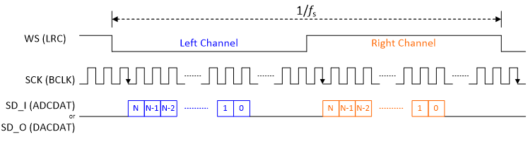
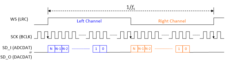
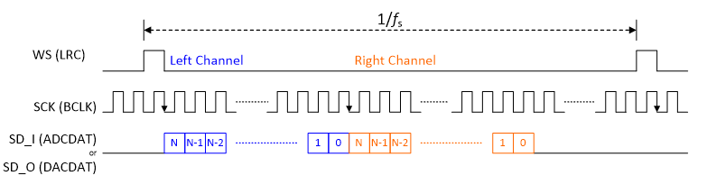
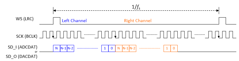
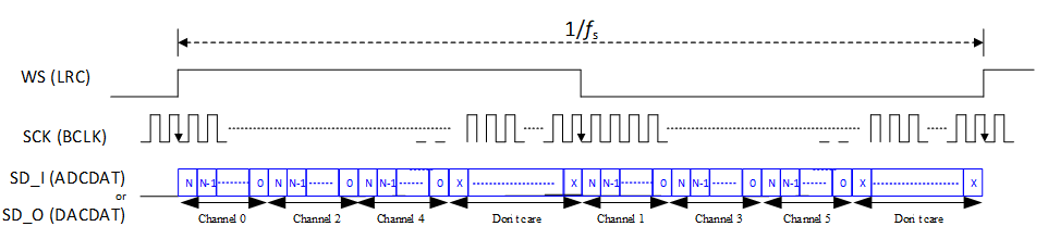
SPORT fs and phase counter is shown below:
SPORT fs counter and phase counter under SPORT CLK
SPORT CLK=98.304MHz/45.1584MHz. When the SPORT CLK is 98.304M, and on every rising edge or falling edge of LRCLK, the phase counter will accumulate once in one SPORT clock cycle, the accuracy of phase counter can reach 10ns.
Phase counter can start on the falling edge of LRCLK, and it increments by one at each SPORT CLK. On the next falling edge of LRCLK, phase counter will be reset to 0 and then start to count again.
Phase counter also can start on the rising edge of LRCLK, the rest is similar to the description above.
In master mode LRCLK is divided by SPORT CLK. In slave mode SPORT LRCLK is supported by master.
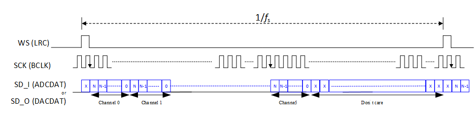
SPORT fs counter and phase counter under SPORT CLK is shown below:
Note
N=SPORTCLK/LRCLK
LRCLK start and stop detect: in slave mode, SPORT can use SPORT clock to monitor the start and stop of LRCLK.
Start condition: detect the rising edge or falling edge(default) of LRCLK. The implementation steps are as follows:
Stop condition: the phase counter is accumulated to a settable threshold. The implementation steps are as follows:
SPORT direct mode feature:
Used for data transmission between different sports without CPU and DMA involved in data transfer.
When two sports work in direct mode, clock needs to be at the same frequency.
SPORT FIFO:
TX_FIFO_0 and TX_FIFO_1 are two asynchronous ping-pong FIFO. Each FIFO is depth=32 and width=32, so 2*32*4bytes=64words.
RX_FIFO_0 and RX_FIFO_1 are two asynchronous ping-pong FIFO. Each FIFO is depth=32 and width=32, so 2*32*4bytes=64words.
6/8 channels for data transmission, FIFO0 and FIFO1 would be used. Two FIFOs will request at the same time, and four SPORTs will produce 16 requests at the same time.
WIFI TSF
WIFI TSF start SPORT
MAC sends interrupt to audio, and hardware will automatically start playing in audio side. The hardware delay is tens of nanoseconds. There is no need to wait for software to set MAC to send interrupt to open the following two bit functions.
Hardware latch SPORT counter when it detects a change in the TSFT specified bit, software specifies the bits.
The latch period is optional: 1.024/ 2.048/ 4.096 ……/ 131.072.
SPORT0 is for internal digital microphone interface and external I2S interface
SPORT1 is only for external I2S interface.
Not support LRCLK start and stop detect
Not support SPORT fs counter and phase counter under SPORT CLK
Support WIFI TSF,but not support WIFI TSF start SPORT
SPORT0 is for internal digital microphone interface and external I2S interface
SPORT1 is only for external I2S interface.
Not support LRCLK start and stop detect
Not support SPORT fs counter and phase counter under SPORT CLK
Not support WIFI TSF
SPORT0 is for internal digital microphone interface and external I2S interface
SPORT1 is only for external I2S interface.
Not support LRCLK start and stop detect
Not support SPORT fs counter and phase counter under SPORT CLK
Not support WIFI TSF
SPORT0 is for internal digital microphone interface and external I2S interface
SPORT1 is only for external I2S interface.
Not support LRCLK start and stop detect
Not support SPORT fs counter and phase counter under SPORT CLK
Not support WIFI TSF
SPORT0/1 is for internal audio codec and not support Multi-IO mode.
SPORT2/3 is for external I2S interface.
Not support LRCLK start and stop detect
Not support SPORT fs counter and phase counter under SPORT CLK
Only CHIP_DCUT supports WIFI TSF, but not support WIFI TSF start SPORT
SPORT0 is for internal digital microphone interface and external I2S interface.
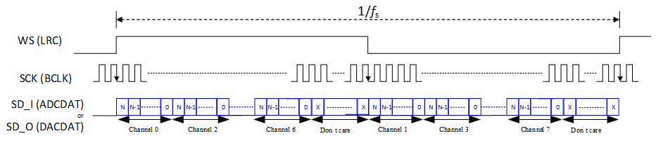
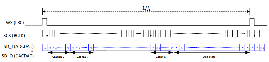
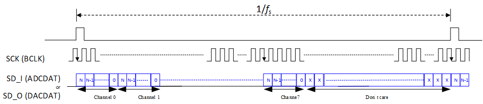
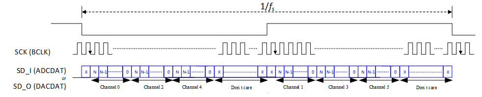
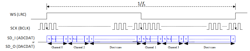
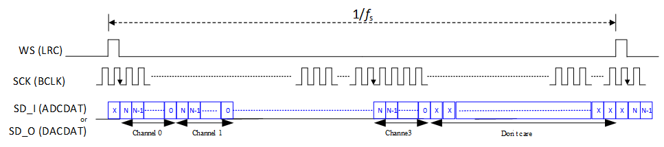
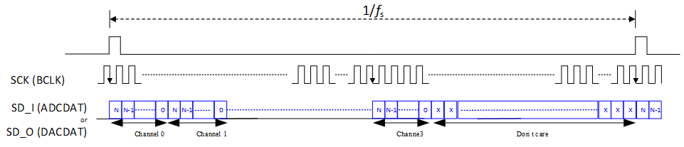
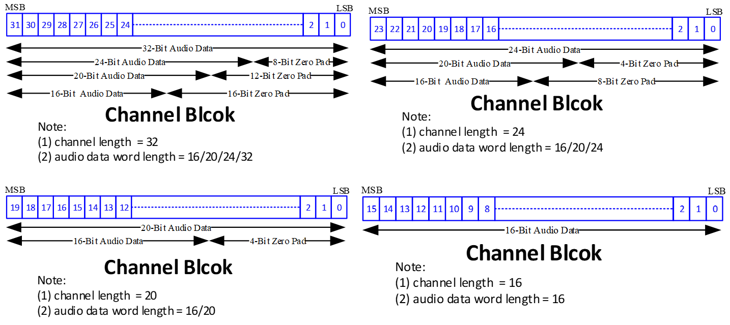
The I2S interface supports I2S(Philips)format, Left-justified(MSB)format, Right-justified(LSB)format, PCM, and TDMmode. Software can select any mode by setting the I2S control register. The following figures show the I2S data format.
The data PIN DIO[3:0] of I2S can be used as output or input. It can be set as input or output in the corresponding part of I2S in the PAD register. I2S data pinmux is shown below.
The data PIN DIO[3:0] of I2S can be used as output or input. It can be set as input or output in the corresponding part of I2S in the PAD register. I2S data pinmux is shown below.
The data PIN DIO[3:0] of I2S can be used as output or input. It can be set as input or output in the corresponding part of I2S in the PAD register. I2S data pinmux is shown below.
The data PIN DIO[3:0] of I2S can be used as output or input. It can be set as input or output in the corresponding part of I2S in the PAD register. I2S data pinmux is shown below.
The data PIN DIN[3:0] of I2S is used as input.
The data PIN DOUT[3:0] of I2S is used as output.
The data PIN DIO[3:0] of I2S can be used as output or input. It can be set as input or output in the corresponding part of I2S in the PAD register. I2S data pinmux is shown below.
The digital microphone (DMIC) interface is for digital microphone, and supports 2-channel digital microphone recording. The following figure shows the details block of digital microphone interface.
The audio codec is a high-performance, up to 4-channel I2S interface audio codec. The transmitted data can be from digital microphone input. Mono high-performance DAC are included.
Two smart digital mic interfaces are supported to make low jitter clock output and decimation filter for up to four digital mics. Independent digital voice controllers are provided in each channel.
PDM interface is supported for PDM digital speaker power amplifier.
An energy-based VAD module is built-in.
The audio codec is a high-performance, up to 4-channel I2S interface audio codec. The transmitted data can be from analog input or digital microphone input. The received data can stream to line output. Three channels analog ADCs and Mono high-performance DAC are included.
Audio codec integrates three ADCs with one mic bias voltage and mic boost amplifier to deliver valid channel data. The analog input port MICIN1_P/N ~ MICIN3_P/N is designed as full differential microphone pins or single-ended line-in pins. Two smart digital mic interfaces are supported to make low jitter clock output and decimation filter for up to four digital mics. Independent digital voice controllers are provided in each channel.
Audio codec integrates mono DAC with different output which actions as an input signal of headset or speaker power amplifier. And also a PDM interface is supported for PDM digital speaker power amplifier.
An energy-based VAD module is built-in.
The audio codec is a high-performance, low-power, up to 8-channel I2S interface audio codec. The transmitted data can be from analog input or digital microphone input. The received data can stream to line output. Five channels analog ADCs can work in low power mode and normal mode. In low power and normal mode, THD+N of five channels ADCs all are about -80dB, and SNR can reach 98dBA. Two high-performance DACs are included, and THD+N of which are all about -85dB, and SNR can reach 98dBA.
Audio codec integrates five ADCs with independent mic bias voltage and mic boost amplifier to deliver valid channel data that channel crosstalk can be eliminated. The analog input port MIC0_P/N ~ MIC4_P/N is designed as full differential microphone pins or single-ended line-in pins. Four smart digital mic interfaces are supported to make low jitter clock output and decimation filter for up to eight digital mics. Independent digital voice controllers are provided in each channel.
Audio codec integrates two DACs with different output which actions as an input signal of headset or speaker power amplifier. And also a PDM interface is supported for PDM digital speaker power amplifier.
Audio codec includes several DSP features such as a high-pass filter, mixer, Equalizer, and volume control. The 10-band parametric Equalizer contains 10 independent filters with programmable gain, center frequency and bandwidth to tailor the frequency characteristics of the embedded playback system according to user preferences. The 5-band parametric Equalizer contains 5 independent filters with programmable gain, center frequency and bandwidth to tailor the frequency characteristics of the embedded record system according to user preferences.
The digital microphone (DMIC) interface is for digital microphone, and supports 2-channel digital microphone recording. The following figure shows the details block of digital microphone interface.
The following figure shows the recording data path of digital microphone interface. In the recording path, the input source is 2-channel DMIC.
The following figure shows the recording data path of audio codec. In the recording path, the input source can be selected DMIC 0-3, and MUSIC_OUT.
DMIC 0-3 is the data from 4 channel digital microphones.
MUSIC_OUT is the data from DAC SDM out for AEC reference signal.
The following figure shows the recording data path of audio codec. In the recording path, the input source can be selected from ADC 1-3, DMIC 0-3, and MUSIC_OUT.
ADC 1-3 is the data from 3 channel analog ADC
DMIC 0-3 is the data from 4 channel digital microphones.
MUSIC_OUT is the data from DAC SDM out for AEC reference signal.
The following figure shows the recording data path of audio codec. In the recording path, the input source can be selected from ADC 0-4, DMIC 0-7, and MUSIC_OUT.
ADC 0-4 is the data from 5 channel analog ADC
DMIC 0-7 is the data from 8 channel digital microphones.
MUSIC_OUT is the data from DAC SDM out.
The following figure shows the recording data path of digital microphone interface. In the recording path, the input source is 2-channel DMIC.
There are three analog ADCs and with up to 3-channel recording paths. You can use three microphones to pass to analog ADCs. Three-channel ADCs has two type analog input ports: microphone input and line input, which all support differential and single end.
The IN1-3P/N are microphone-type input ports. The input port can be configured to differential input or single-ended input. The microphone input port has its microphone bias and microphone boost. The low noise microphone bias can improve recording performance and enhance recording quality. Built-in short current detection scheme can be used for switch detection. Multi-step microphone boost gain is easy to use for microphone applications. The following figure shows the recording analog block.
A boost amplifier is provided in the input path to the ADC, which can be used manually with 5dB step from 0dB to 40dB, to keep the recording volume constant.
The recording part includes one programmable microphone bias output, capable of providing output voltages of 1.8V with 3mA output-current drive capability. It can be powered down completely when not needed for power saving. The following figure shows the function block of MICBIAS.
There are five analog ADCs and with up to 5-channel recording paths. You can use five microphones to pass to analog ADCs. Five channel ADCs has two type analog input ports: microphone input and line input, which all support differential and single-ended.
The IN0-4P/N are microphone-type input ports. The input port can be configured to differential input or single-ended input. The microphone input port has its microphone bias and microphone boost. The low noise microphone bias can improve recording performance and enhance recording quality. Build-in short current detection scheme can be used for switch detection. Multi-step microphone boost gain is easy to use for microphone applications. The following figure shows the recording analog block.
A boost amplifier is provided in the input path to the ADC, which can be used manually with 5dB step from 0dB to 40dB, to keep the recording volume constant.
There are up to 8-channel digital microphone interface which shares the digital path with AMIC ADC.
The recording part includes five programmable microphone bias outputs (MICBIAS0, MICBIAS1, MICBIAS2, MICBIAS3, MICBIAS4), capable of providing output voltages of 1.8V with 3mA output-current drive capability. In addition, the MICBIAS outputs may be programmed to be switched to AVCC_DRV directly through an on-chip switch, and it can be powered down completely when no need for power saving. The following figure shows the function block of MICBIAS.
Note
In low power mode, the power supply of external AMIC should be switched to AVCC_DRV. You can configure GPIO<16:12> to output HIGH to realize it. This is equivalent to that the phase inverter outputs high level, and software conduction resistance is about 33Ω.
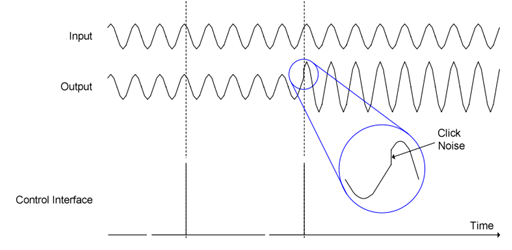
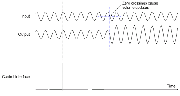
In order to prevent this click noise, a zero-crossing function is provided. When enabled, this will cause the volume to update only when a zero crossing occurs, minimizing click noise, as shown below.
The equalizer block cascades 0-5 bands of equalizer to tailor the frequency characteristics of the recording system according to user preferences and to emulate environment sound.
DC remove function block
A high pass filter is implemented for dc offset. The high pass filter is mainly for ADC recording used. The cut-off frequency of filter is programmable and is varied according to different sample rates. The filter is used to remove DC offset at normal conditions.
Silence detector block
The Silence detector is used to reduce the noise floor for DAC path or ADC path. When the input signal is below silence level, the input signal will be reduced to suppress the background noise. The reducing level can be set by registers.
Build-in 1-channel PDM out interface, connected to a PDM speaker amplifier to playback.
Build-in 1-channel sigma-delta DAC is an on-chip Sigma-Delta Modulator, and a 24-bit input high-performance current steering DAC is composed of it. The analog part controls the current cell by the signal from digital part, and changes digital signal to analog signal and sends to Power Amplifier (PA).
Build-in 1-channel sigma-delta DAC is an on-chip Sigma-Delta Modulator, and a 24-bit input high-performance current steering DAC is composed of it. The analog part controls the current cell by the signal from digital part, and changes digital signal to analog signal and sends to Power Amplifier (PA).
Build-in 2-channel sigma-delta DAC is an on-chip Sigma-Delta Modulator, and a 24-bit input high-performance current steering DAC is composed of it. The analog part controls the current cell by the signal from digital part, and changes digital signal to analog signal and sents to Power Amplifier (PA).
Built-in a PDM interface, for PDM speaker amplifier, the interface will support mono speaker.
Built-in high-performance stereo current steering DAC, and with stereo headphone driver amplifiers, the amplifiers support differential output and an anti-pop circuit can suppress the noise of amplifier when power up effectively. The headphone driver amplifiers include 4 level volume control, which decreases 3dB by one step. LOUT signal is from DAC_L.
Built-in a PDM interface, for PDM speaker amplifier, the interface will support mono speaker.
Built-in high-performance stereo current steering DAC, and with stereo headphone driver amplifiers, the amplifiers support differential output and an anti-pop circuit can suppress the noise of amplifier when power up effectively. The headphone driver amplifiers include 4 level volume control, which decreases 3dB by one step. LOUT signal is from DAC_L and ROUT signal is from DAC_R.
Playback path for sample rate 8K,11.025K,12K,16K,32K,22.05K,44.1K 48kHz,88.2K,96kHz, 176.4K,192K
ASRC supports up to 96kHZ sample rate
The DAC digital part support digital volume control, and the gain is between 0dB and -65.625dB in 0.375dB/step.
There is a high pass filter for DC offset, the cut-off frequency of filter is programmable and is varied according to different sample rates.
Zero crossing function, this function is the same as ADC zero crossing.
Silence detector block
The Silence detector is used to reduce the noise floor for DAC path or ADC path. When the input signal is below silence level, the input signal will be reduced to suppress the background noise. The reducing level can be set by registers.
PDM interface
Test tone
Built-in a test tone module, the tone frequency can be configured by (fs/192)*(tone_fc_sel+1)kHz, and the tone gain can be configured by 0 ~ 6.02*(gain_sel)dB.
Playback path for sample rate 8K,11.025K,12K,16K,32K,22.05K,44.1K 48kHz,88.2K,96kHz, 176.4K,192K
Asynchronous Sample Rate Converters (ASRC)
The DAC digital part support digital volume control, and the gain is between 0dB and -65.625dB in 0.375dB per step.
There is a high pass filter for DC offset, the cut-off frequency of filter is programmable and is varied according to different sample rates.
Zero-crossing function, which is the same as ADC zero-crossing.
PDM interface
Test tone
Built-in a test tone module, the tone frequency can be configured by (fs/192)*(tone_fc_sel+1)kHz, and the tone gain can be configured by 0~6.02*(gain_sel)dB
Channel L and channel R mix
Before streaming to DAC, channel L data and channel R data are mixed, then streamed to DAC_L channel and DAC_R channel.
VAD (Voice Activity Detection) is a low-energy voice detect IP. It supports voice trigger. Once the VAD function is enabled, it will automatically sample the voice and detect the voice energy above the threshold value or not, even the processor is in sleep mode.
The overall design of VAD mainly includes two aspects, one is the generation of wake-up interrupt, to wake up the processor; the other is the transmission of voice data after wake-up, to let the processor timely access to audio data for keyword recognition.
VAD data source may be up to four analog microphones, and up to eight digital microphones. The VAD can configure software to choose which audio source to use as input. An APB configuration interface is also supported. When the VAD successfully recognizes a human voice in CPU low power mode, an interrupt is generated and reported to the CPU.
SRAM is used to store audio data buffer during power consumption. It is 128KB in size and supports 64 bits read/write. The data source is parallel to the VAD’s audio data source and is also audio data after the MUX.
At the same time, SRAM can also be read and written by KM0, KM4 and CA32 at workflow.