Introduction
GPIO is a programmable general purpose programming I/O peripheral.
The following functional groupings of the main interfaces to the GPIO block is illustrated as below:
APB interface to or from APB bridge
External data interface to or from I/O pads
Interrupt interface to or from interrupt controller

The chip supports two independent GPIO IP: Port A (0~31), Port B (0~31), which controls the output data and direction of external I/O pads. Also, it can read back the data on external pads using memory-mapped registers.
Port A/B can be programmed to accept external signals as interrupt sources on any bits of the signal. The type of interrupt is programmable with one of the following settings:
Each general purpose I/O port has four 32-bit data registers (gpio_swportx_dr, gpio_swportX_ddr, gpio_swportX_ctrl, gpio_ext_portx);
Each port has eleven 32-bit interrupt related registers (gpio_int_en, gpio_int_mask, gpio_int_type, gpio_int_polarity, gpio_int_status, gpio_int_status_raw, gpio_debounce, gpio_int_eoi, gpio_int_ls_sync, gpio_int_bothedge, gpio_db_div_cnt).
Features
GPIO supports the following features:
Up to 96 independently configurable signals and 32 signals for each port
Separate data register and data direction register for each signal
Configurable software control for each signal, or for each bit of each signal
Independently controllable signal bits
Interrupt mode
Option to generate single or multiple interrupts
Configurable debounce logic with an external slow clock to debounce interrupts
Functional Description
This chapter describes the basic functional operation of the GPIO.
Data Read and Write Control
GPIO controls the output data and direction of external I/O pads. It also can read back the data on external pads using memory-mapped registers. Software can control each signal over the APB bus interface. The data and control flow for a signal are shown below.

Note
Each bit in each signal is individually controllable. Therefore, each register can be regarded as N individual registers, where N is the signal width with the range from 0 to 31.
PORTx in this chapter means Port A (0~31), Port B (0~31), where x is A or B.
GPIO Direction
The direction of the external I/O pad is controlled by a write to the PORTx data direction register (gpio_swportx_ddr ). This output signal controls the direction of an external I/O pad.
GPIO Write
When configured as output, the data written to the PORTx data register (gpio_swportx_dr ) drives the output buffer of the I/O pad.
GPIO Read
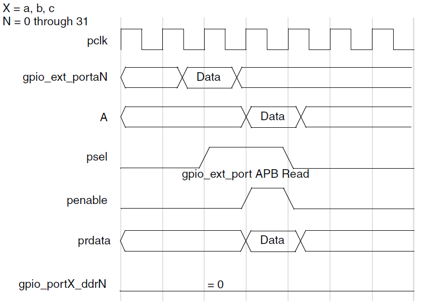
The data on the external GPIO signal is read by an APB read of the memory-mapped register, gpio_ext_portx . An APB read to the gpio_ext_portx register provides either the data on the gpio_ext_portx control lines or the contents of the gpio_swportx_dr , depending on whether gpio_ext_portx is configured as an input or output, the following occurs:
Input: read the values on the signal
Output: read the data register for PORTx
The gpio_ext_portx register is read-only, meaning that it cannot be written from the APB software interface.
The following figure shows a timing diagram of a read to the gpio_ext_portx memory map registers when the direction is set to input and the metastability registers are included, which brings a data delay of the port line.
Note
The maximum data rate that can be read back on consecutive reads from gpio_ext_portx must be less than pclk/2. Two pclk cycles per read access is required due to the non-pipelined nature of the APB. The assumption is that the APB bridge does not lose ownership of the AHB during consecutive accesses when PCLK=HCLK.
Interrupts
External signals can be configured as interrupt sources on any bits of the signal. The type of interrupt is programmable with one of the following settings:
Level-sensitive interrupt:
Active-high level
Active-low level
Edge-trigger interrupt:
Rising edge
Falling edge
Both edge
The interrupts can be masked by programming the gpio_intmask register. The interrupt status can be read before masking (called raw status from gpio_int_status_raw ) and after masking (gpio_int_status ).
To configure PORTx for interrupts, the data direction must be set to Input. If the data direction register is reprogrammed to Output, then any pending interrupts will not be lost. However, no new interrupts are generated.
The following figure illustrates how the interrupts are generated and how the data flows. The signal names in the diagram correspond to either I/O signals or memory-mapped registers.
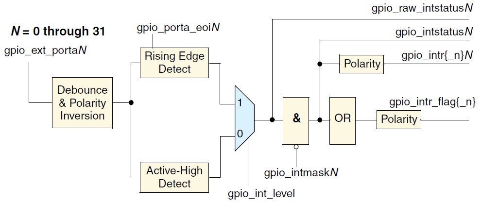
The interrupts are also combined into a single interrupt output signal, which has the same polarity as the individual interrupts. Either individual interrupts (gpio_intr or gpio_intr_n) or a single combined interrupt (gpio_intr_flag or gpio_intr_flag_n) can be generated. In order to mask the combined interrupt, all individual interrupts have to be masked. The single combined interrupt does not have its own mask bit.
The simplest connection scheme is where the combined interrupt gpio_intr_flag is generated by ORing together the bits of the gpio_intr bus.
When only the combined interrupt request is used, then the gpio_status register must be read in the interrupt service routine (ISR) to find the source of the interrupt. Then it is up to the processor to prioritize these pending interrupt requests.
When the individual interrupts lines are connected directly to the interrupt controller, then the gpio_status register does not have to be read by the ISR.
Debounce Operation (optional)
If the user has configured the interrupt feature, GPIO can be configured to either include or exclude a debounce capability using the GPIO_DEBOUNCE parameter. The external signal can be debounced to remove any spurious glitches that are less than one period of the external debouncing clock.
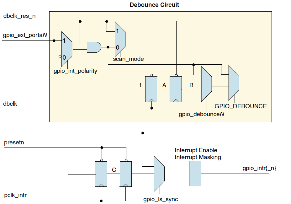
The following figure shows an RTL diagram of the debounce circuitry. The timing diagram shows an active-high input signal on gpio_ext_portxN. The polarity of the input signal detection is controlled by the memory-mapped signal, gpio_int_polarity. For a falling-edge or active-low-sensitive input, the input is then inverted and the same debounce logic is used as for rising-edge or active-high level-sensitive interrupts.
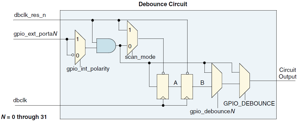
dbclk_res_n signal is asynchronously asserted and synchronously de-asserted to the debounce clock, dbclk.
presetn, the system reset signal, is asynchronously asserted and synchronously de-asserted to pclk; synchronization must be external to the component.
The pclk and dbclk signals are assumed to be asynchronous to each other.
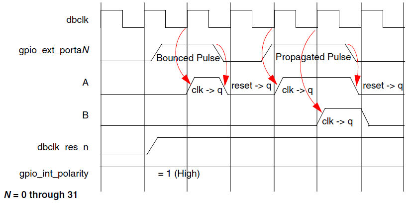
When input interrupt signals are debounced using a debounce clock, the signals must be active for a minimum of two cycles of the debounce clock to guarantee that they are registered. Any input pulse widths less than a debounce clock period are bounced. A pulse width between one and two debounce clock widths may or may not propagate, depending on its phase relationship to the debounce clock. If the input pulse
spans two rising edges of the debounce clock, it is registered. If it spans only one rising edge, it is not registered.
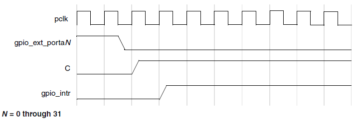
The timing diagram below shows both cases: the input signal being bounced, and later, a propagated input signal. If GPIO supports debounce, then debouncing input signals on Port A can be enabled or disabled under software control.
Debounce timing with asynchronous reset flip-flops
Note
The use of the debounce circuitry increases interrupt latency by two clock cycles of the debounce clock.
The debounce circuitry works with only asynchronous reset flip-flops.
Synchronization of Interrupt Signals to System Clock
Interrupt signals can be internally synchronized to a system clock, pclk_intr. Synchronization to pclk_intr must occur for edge-detect signals. Edge-detected interrupts to the processor are always synchronous to the system bus clock. For level-sensitive interrupts, synchronization is optional and under software control.
The pclk_intr signal is needed for systems that may have the GPIO pclk bus clock gated off, but the system still wants to detect interrupts. It is assumed that this clock is synchronous to pclk. If interrupt detection is required only when pclk is running, then pclk_intr and pclk can be connected to the same clock source. If the system employs a gated pclk to the GPIO, pclk_intr needs to be running for interrupt detection to occur.
The gpio_intrclk_en output signal is asserted when either edge-sensitive interrupts or level-sensitive interrupts requiring synchronization are enabled in the GPIO block. Both cases require a clock for detection. Therefore, this signal can cause the external clock generator block to generate pclk_intr.
Interrupt Edge Detection
For edge-detected interrupts, the ISR can clear the interrupt by writing 1 to the gpio_porta_eoi register for the corresponding bit to disable the interrupt. This write also clears the interrupt status and raw status registers. It is recommended that the interrupt source be cleared prior to writing to the gpio_porta_eoi register. Writing to the gpio_porta_eoi register has no effect on level-sensitive interrupts. For combined interrupt request connection, there are no restrictions on the number of edge-detected interrupts that can be cleared simultaneously by writing multiple 1’s to the gpio_porta_eoi register.
Single Edge
The following figure shows an RTL diagram of the synchronization and edge detection of interrupt sources on gpio_ext_portaN signals, when GPIO_INT_BOTH_EDGE =1.
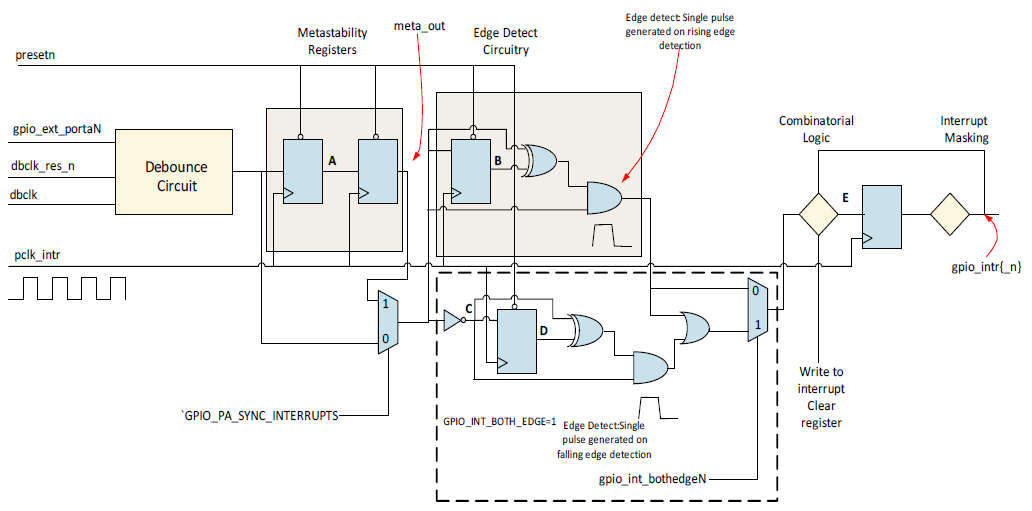
Note
Metastability part is default included.
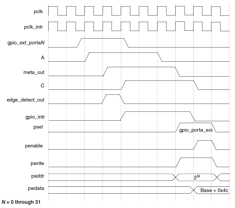
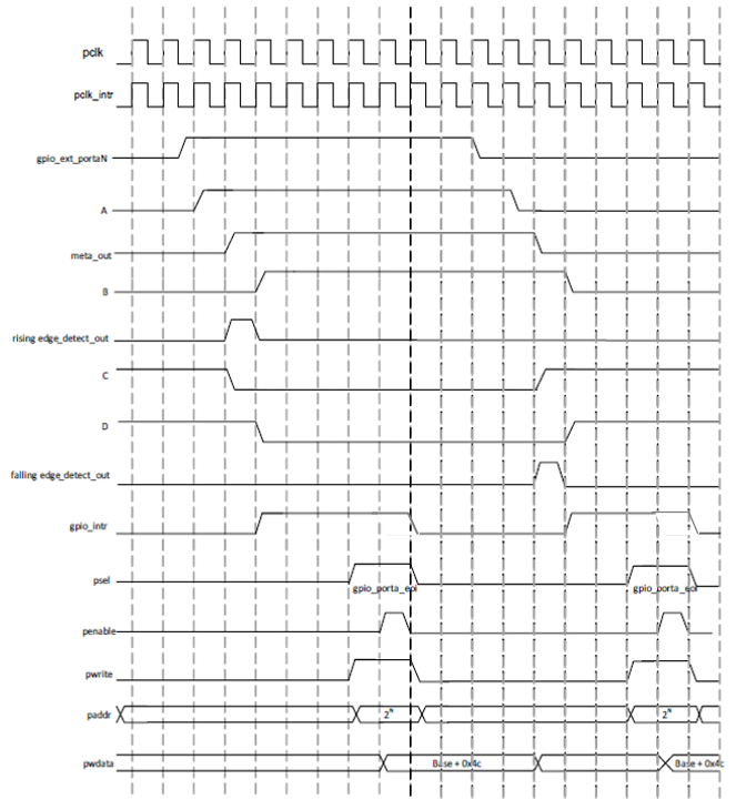
Interrupt edge detection and interrupt clear timing (GPIO_SYNC_PA_INTERRPUTS = 1, metastability included) shows a timing diagram in which an interrupt is generated on the rising edge of input on Port A; this is where the debounce logic is disabled and metastability registers are included. It also shows how an interrupt is cleared by a write to the interrupt clear register.
A case may arise where the Interrupt Service Routine (ISR) writes to the interrupt clear register to clear an existing interrupt during the same clock cycle in which a new interrupt is detected. In such a case, writing to the interrupt clear register clears only the first interrupt. The second interrupt is not lost, since setting an interrupt has a higher priority than clearing it.
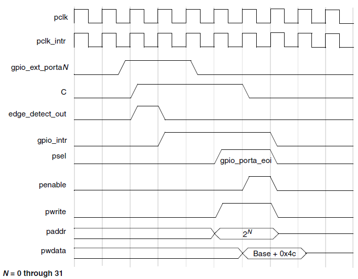
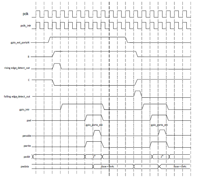
Interrupt edge detection and interrupt clear timing (GPIO_SYNC_PA_INTERRPUTS = 0, metastability removed) shows a timing diagram similar to the figure Interrupt edge detection and interrupt clear timing (GPIO_SYNC_PA_INTERRPUTS = 1, metastability included) except that metastability registers are removed. It also shows how an interrupt is cleared by a write to the interrupt clear register.
Note
Since the Metastability registers are removed from the path, A and B waveforms, shown in Interrupt edge detection and interrupt clear timing (GPIO_SYNC_PA_INTERRPUTS = 1, metastability included), no longer exist, and all subsequent signal delays are reduced by two clock cycles.
Interrupt edge detection and interrupt clear timing (GPIO_SYNC_PA_INTERRPUTS = 1, metastability included)
Interrupt edge detection and interrupt clear timing (GPIO_SYNC_PA_INTERRPUTS = 0, metastability removed)
The following figure shows such a case where the debounce logic is unused. In this timing diagram, meta_out and edge_detect_out are the outputs of the second metastability register and the edge detect logic, respectively. The second edge detection occurs on the same cycle as the write to the interrupt clear register. In this example, the write to the interrupt clear register does not clear the second interrupt, and the gpio_intr{_n} signal is not de-asserted.
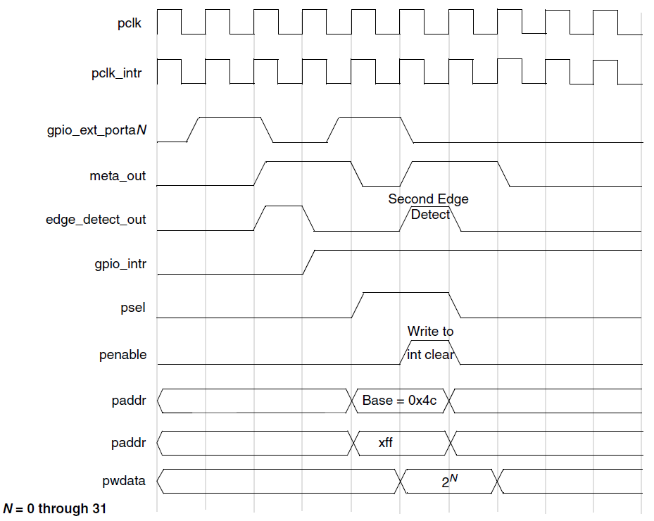
Write to interrupt clear register, coincident with detection of new interrupt
Both Edges
Interrupt detection logic for both the rising edge and the falling edge is available only when GPIO_INT_BOTH_EDGE = 1 and this logic detects the interrupt on both the rising edge and the falling edge when the gpio_int_bothedge register is programmed to 1.
The following figure shows the synchronization and edge detect interrupt generation of the interrupt sources on gpio_ext_portaN signals when GPIO_INT_BOTH_EDGE = 0.
The following figure shows a timing diagram where an interrupt is generated on both the rising edge and the falling edge of input on Port A, that is, with GPIO_INT_BOTH_EDGE = 1 and gpio_int_bothedge programmed to detect both edges. In this scenario, debounce logic is disabled and metastability registers are included. This figure also shows how an interrupt is cleared by a write to the interrupt clear register.
Interrupt edge detection and interrupt clear timing (GPIO_SYNC_PA_INTERRPUTS = 1 and GPIO_INT_BOTH_EDGE =1, metastability included)
The following figure shows a timing diagram similar to the figure Interrupt edge detection and interrupt clear timing (GPIO_SYNC_PA_INTERRPUTS = 1 and GPIO_INT_BOTH_EDGE =1, metastability included), except that in this scenario, metastability registers are removed.
Interrupt edge detection and interrupt clear timing (GPIO_SYNC_PA_INTERRPUTS = 0 and GPIO_INT_BOTH_EDGE =1, metastability removed)
Level-Sensitive Interrupts
If level-sensitive interrupts cause the processor to interrupt, then the ISR can poll the gpio_rawint status register until the interrupt source disappears, or it can write to the gpio_intmask register to mask the interrupt before exiting the ISR. If the ISR exits without masking or disabling the interrupt prior to exiting, then the level-sensitive interrupt repeatedly requests an interrupt until the interrupt is cleared at the source.
The following figure shows the generation of level-sensitive interrupts. As for edge-detect interrupts, the user can configure GPIO with or without external debounce logic. The debounce circuit below is an example of debounce or remove spurious glitch less than 2 cycles of dbclk.
Level-sensitive interrupt RTL diagram
With level-sensitive interrupts, there is a choice of whether they are synchronized to the interrupt clock pclk_intr or are entirely combinational (aside from the debounce circuit). The selection is done by programming the gpio_ls_sync (GPIO Level Sensitive Synchronous) register.
This is a memory-mapped bit that inserts two metastability registers clocked off of pclk_intr to synchronize the level-sensitive interrupts to pclk_intr. When gpio_ls_sync is not asserted, then there is no guarantee that the interrupt lines are synchronous to pclk_intr. A processor status register may need to be set to indicate asynchronous interrupts. When gpio_ls_sync is asserted, then the pclk_intr clock must be present to pass the interrupt to the interrupt controller block. The gpio_intrclk_en output signal is asserted when level-sensitive interrupts to be synchronized to pclk_intr are selected. The gpio_intrclk_en signal can be used in the clock generation block to turn on pclk_intr.
Note
In active mode, pclk_intr synchronize to pclk is recommended to prevent the production of burrs in the circuit
In sleep mode, if you need to wake up quickly, you can be out of this synchronization to pclk_intr.
The following figure shows the generation of an active-low level-sensitive interrupt where the debounce circuitry is disabled.
Active-low level-sensitive interrupt generation timing
Registers
The following table lists the memory map of the GPIO register. The base address are:
GPIO_A:
0x4101_0000GPIO_B:
0x4101_0400
Name |
Address offset |
Access |
Description |
|---|---|---|---|
000h |
R/W |
||
004h |
R/W |
||
008h |
R |
||
030h |
R/W |
||
034h |
R/W |
||
038h |
R/W |
||
03Ch |
R/W |
||
040h |
R |
||
044h |
R |
||
048h |
R/W |
||
04Ch |
R/W |
||
050h |
R |
||
060h |
R/W |
||
064h |
R |
||
068h |
R/W |
||
06Ch |
R |
||
078h |
R |
||
0FCh |
R |
REG_GPIO_DR
Name : Port data register
Size : 32
Address offset : 000h
Read/write access : R/W
Bit |
Symbol |
Access |
Reset |
Description |
|---|---|---|---|---|
31:0 |
PORT_DATA |
R/W |
0 |
Values written to this register are output on the I/O signal s for Portx if the corresponding data direction bits for Por tx are set to Output mode and the corresponding control bit for Portx is set to software mode. The value read back is eq ual to the last value written to this register. |
REG_GPIO_DDR
Name : Port data direction register
Size : 32
Address offset : 004h
Read/write access : R/W
Bit |
Symbol |
Access |
Reset |
Description |
|---|---|---|---|---|
31:0 |
PORT_DATA_DIRECTION |
R/W |
0 |
Values written to this register independently control the di rection of the corresponding data bit in Portx. The default direction can be configured as input or output after system reset through the GPIO_DFLT_DIR_x parameter.
|
REG_GPIO_CTL
Name : Port data source register
Size : 32
Address offset : 008h
Read/write access : R
Bit |
Symbol |
Access |
Reset |
Description |
|---|---|---|---|---|
31:0 |
RSVD |
R |
- |
Reserved |
REG_GPIO_INT_EN
Name : Port interrupt enable register
Size : 32
Address offset : 030h
Read/write access : R/W
Bit |
Symbol |
Access |
Reset |
Description |
|---|---|---|---|---|
31:0 |
GPIO_INT_EN |
R/W |
0 |
Allows each bit of Portx to be configured for interrupts. By default, the generation of interrupts is disabled. Whenever a 1 is written to a bit of this register, it configures the corresponding bit on Portx to become an interrupt; otherwise , Portx operates as a normal GPIO signal. Interrupts are dis abled on the corresponding bits of Portx if the correspondin g data direction register is set to Output or if Portx mode is set to Hardware.
|
REG_GPIO_INT_MASK
Name : Port interrupt mask register
Size : 32
Address offset : 034h
Read/write access : R/W
Bit |
Symbol |
Access |
Reset |
Description |
|---|---|---|---|---|
31:0 |
GPIO_INT_MASK |
R/W |
0 |
Controls whether an interrupt on Portx can create an interru pt for the interrupt controller by not masking it. By defaul t, all interrupts bits are unmasked. Whenever a 1 is written to a bit in this register, it masks the interrupt generation capability for this signal; otherwise interrupts are allowed through. The unmasked status can be read as well as the resu ltant status after masking.
|
REG_GPIO_INT_TYPE
Name : Port interrupt trigger type register
Size : 32
Address offset : 038h
Read/write access : R/W
Bit |
Symbol |
Access |
Reset |
Description |
|---|---|---|---|---|
31:0 |
GPIO_INT_TYPE |
R/W |
0 |
Controls the type of interrupt that can occur on Portx. Whenever a 0 is written to a bit of this register, it config ures the Interrupt type to be level-sensitive; otherwise, it is edge -sensitive.
|
REG_GPIO_INT_POLARITY
Name : Port interrupt polarity register
Size : 32
Address offset : 03Ch
Read/write access : R/W
Bit |
Symbol |
Access |
Reset |
Description |
|---|---|---|---|---|
31:0 |
GPIO_INT_POLARITY |
R/W |
0 |
Controls the polarity of edge or level sensitivity that can occur on input of Portx. Whenever a 0 is written to a bit of this register, it configures the interrupt type to falling- edge or active-low sensitive; otherwise, it is rising-edge or active-high sensitive.
|
REG_GPIO_INT_STATUS
Name : Port interrupt status register
Size : 32
Address offset : 040h
Read/write access : R
Bit |
Symbol |
Access |
Reset |
Description |
|---|---|---|---|---|
31:0 |
GPIO_INT_STATUS |
R |
0 |
Interrupt status of Portx. |
REG_GPIO_INT_STATUS_RAW
Name : Port raw interrupt status register
Size : 32
Address offset : 044h
Read/write access : R
Bit |
Symbol |
Access |
Reset |
Description |
|---|---|---|---|---|
31:0 |
GPIO_RAW_INT_STATUS |
R |
0 |
Raw interrupt status of Portx (premasking bits). |
REG_GPIO_DEBOUNCE
Name : Port interrupt debounce register
Size : 32
Address offset : 048h
Read/write access : R/W
Bit |
Symbol |
Access |
Reset |
Description |
|---|---|---|---|---|
31:0 |
GPIO_DEBOUNCE_EN |
R/W |
0 |
Controls whether an external signal that is the source of an interrupt needs to be debounced to remove any spurious glitc hes. Writing a 1 to a bit in this register enables the debou ncing circuitry. A signal must be valid for two periods of a n external clock before it is internally Processed.
This register is available only if Portx is configured to ge nerate interrupts (GPIO_PORTA_INTR = Include (1)) and when t he debounce logic is included (GPIO_DEBOUNCE = Include (1)). |
REG_GPIO_INT_EOI
Name : Port edge type interrupt clear register
Size : 32
Address offset : 04Ch
Read/write access : R/W
Bit |
Symbol |
Access |
Reset |
Description |
|---|---|---|---|---|
31:0 |
GPIO_INT_EOI |
R/W |
0 |
Controls the clearing of edge type interrupts from Portx. When a 1 is written into a corresponding bit of this registe r, the interrupt is cleared. All interrupts are cleared when Portx is not configured for interrupts.
|
REG_GPIO_EXT_PORT
Name : External Port data register
Size : 32
Address offset : 050h
Read/write access : R
Bit |
Symbol |
Access |
Reset |
Description |
|---|---|---|---|---|
31:0 |
GPIO_EXT_PORTA |
R |
0 |
When Portx is configured as Input, then reading this locatio n reads the values on the signal. When the data direction of Portx is set as Output, reading this location reads the data register for Portx. |
REG_GPIO_ITN_LS_SYNC
Name : Port level interrupt synchronization
Size : 32
Address offset : 060h
Read/write access : R/W
Bit |
Symbol |
Access |
Reset |
Description |
|---|---|---|---|---|
31:1 |
RSVD |
R |
- |
Reserved |
0 |
GPIO_LEVEL_SYNC |
R/W |
0 |
Writing a 1 to this register results in all level-sensitive interrupts being synchronized to pclk_intr.
|
REG_GPIO_ID_CODE
Name : Port GPIO ID code register
Size : 32
Address offset : 064h
Read/write access : R
Bit |
Symbol |
Access |
Reset |
Description |
|---|---|---|---|---|
31:0 |
GPIO_ID_CODE |
R |
32’h1 |
This register is available only if Portx is configured to ge nerate interrupts (GPIO_PORTx_INTR = Include (1)) and interr upt detection is configured to generate on both rising and f alling edges of external input signal (GPIO_INT_BOTH_EDGE=In clude (1)). |
REG_GPIO_INT_BOTHEDGE
Name : Port both edge interrupt register
Size : 32
Address offset : 068h
Read/write access : R/W
Bit |
Symbol |
Access |
Reset |
Description |
|---|---|---|---|---|
31:0 |
GPIO_INT_BOTHEDGE |
R/W |
0 |
Controls the edge types of interrupt that can occur on Portx . Whenever a particular bit is programmed to 1, it enables the generation of interrupt on both the rising edge and falling edge of an external input signal corresponding to that bit o n Port. The values programmed in the registers gpio_intype_level and gpio_int_polarity for this particular bit are not considered when the corresponding bit of this register is set to 1. Whenever a particular bit is programmed to 0, the interrupt type depends on the value of the corresponding bits in the g pio_inttype_level and gpio_int_polarity registers.
|
REG_GPIO_VER_ID_CODE
Name : Port GPIO component version register
Size : 32
Address offset : 06Ch
Read/write access : R
Bit |
Symbol |
Access |
Reset |
Description |
|---|---|---|---|---|
31:0 |
GPIO_VER_ID_CODE |
R |
32’h3231302A |
ASCII value for each number in the version, followed by *. F or example 32_30_31_2A represents the version 2.01*. Reset Value: See the releases table in the Release Notes. |
REG_GPIO_DB_DIV_CONFIG
Size : 32
Address offset : 078h
Read/write access : R
Bit |
Symbol |
Access |
Reset |
Description |
|---|---|---|---|---|
31:0 |
RSVD |
R |
- |
Reserved |
REG_GPIO_DUMMY
Size : 32
Address offset : 0FCh
Read/write access : R
Bit |
Symbol |
Access |
Reset |
Description |
|---|---|---|---|---|
31:16 |
RSVD |
R |
- |
Reserved |
15:0 |
DUMMY |
R |
0 |
No real reg, only for run_espec.py |
Programming Considerations
Reading from an unused location or unused bit sin a particular register always returns zeros. There is no error mechanism in the APB.
Programming the GPIO registers for interrupt capability, edge-sensitive or level-sensitive interrupts, and interrupt polarity should be completed prior to enabling the interrupts on Port A/B to prevent spurious glitches on the interrupt lines to the interrupt controller.
If using external debounce function to remove spurious glitches, not expected interrupt may bring into the interrupt controller when enabling the interrupts.
To avoid unexpected interrupt with debounce circuit while re-configure the interrupt trigger mode, you had better wait the debounce time before enabling interrupt again.
Writing to the interrupt clear register clears an edge-detected interrupt and has no effect on a level-sensitive interrupt.
When reading back registers that are no longer present due to configuration parameters settings, 0 is read back. For example, if
APB_DATA_WITDH = 32 bitsandGPIO_PWIDTH_A = 8, then the top 24 bits read back 0.